EECS 470 Cache and Memory Systems Lecture 14 Coverage: Chapter 5.
description
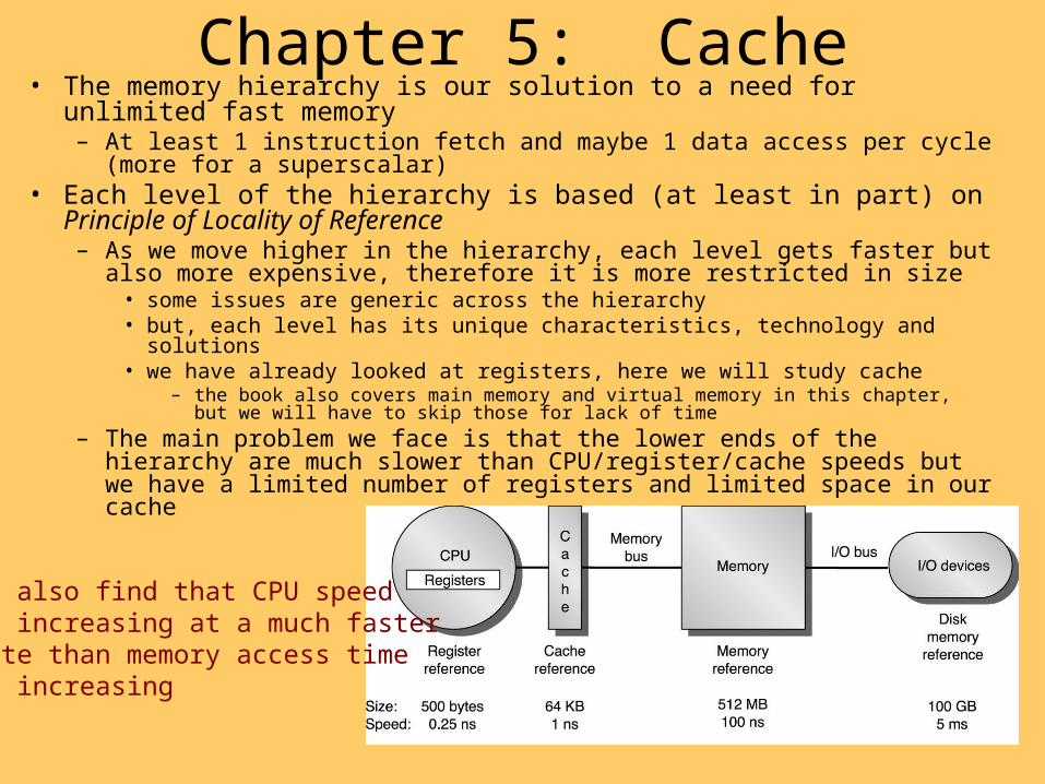
Chapter 5: Cache• The memory hierarchy is our solution to a need for unlimited fast memory
– At least 1 instruction fetch and maybe 1 data access per cycle (more for a superscalar)
• Each level of the hierarchy is based (at least in part) on Principle of Locality of Reference– As we move higher in the hierarchy, each level gets faster but also more expensive,
therefore it is more restricted in size• some issues are generic across the hierarchy• but, each level has its unique characteristics, technology and solutions • we have already looked at registers, here we will study cache
– the book also covers main memory and virtual memory in this chapter, but we will have to skip those for lack of time
– The main problem we face is that the lower ends of the hierarchy are much slower than CPU/register/cache speeds but we have a limited number of registers and limited space in our cache
we also find that CPU speed is increasing at a much faster rate than memory access time is increasing
Effects on memory speed• Memory speed has a direct effect on CPU performance as
indicated by:– CPU execution time = (CPU clock cycles + memory stall cycles) * clock
cycle time• mem stall cycles = IC * mem references per instr * miss rate * miss penalty
– mem references per instr > 1 since there will be the instruction fetch itself, and possible 1 or more data fetches
• whenever an instruction or data is not in registers, we must fetch it from cache, but if it is not in cache, we accrue a miss penalty by having to access the much slower main memory
• A large enough miss penalty will cause a substantial decrease in CPU execute time– Consider the following example
• CPI = 1.0 when all memory accesses are hits• Only data accesses are during loads and stores (50% of all instructions are loads
or stores)• Miss penalty is 25 clock cycles, miss rate is 2%
– How much faster would the computer be if all cache accesses were hits?• CPI = 1.0 without misses• CPI = 1.0 + 100%*2%*25 + 50%*2%*25 = 1.75
– The ideal machine is 75% faster than our “realistic machine”
Four questions• The general piece of memory will be called a block
– Blocks differ in size depending on the level of the memory hierarchy • cache block, memory block, disk block
• We ask the following questions pertaining to both cache, main memory and disk:– Q1: where can a block be placed?– Q2: how is a block found?– Q3: which block should be replaced on a miss?– Q4: what happens on a write?
• Cache is made from SRAMs whereas main memory is made from DRAM– SRAM is faster but much more expensive– SRAM is also used to make registers, the technology is based on flip-flop
circuits• Cache acts as an intermediate between registers and main memory
in the memory hierarchy– Three types of caches: Direct mapped, Associative, Set-associative – Today, we usually have two caches: one for instructions and one for data
• connected to the CPU by two separate ports
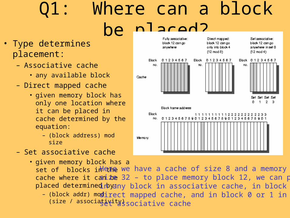
Q1: Where can a block be placed?• Type determines placement:
– Associative cache • any available block
– Direct mapped cache • given memory block has only
one location where it can be placed in cache determined by the equation:
– (block address) mod size
– Set associative cache • given memory block has a set
of blocks in the cache where it can be placed determined by:
– (block addr) mod (size / associativity)
Here we have a cache of size 8 and a memory of size 32 – to place memory block 12, we can put it in any block in associative cache, in block 4 in direct mapped cache, and in block 0 or 1 in a 2 way set associative cache
Q2: How is a block found in cache? Q3: Which block should be replaced?
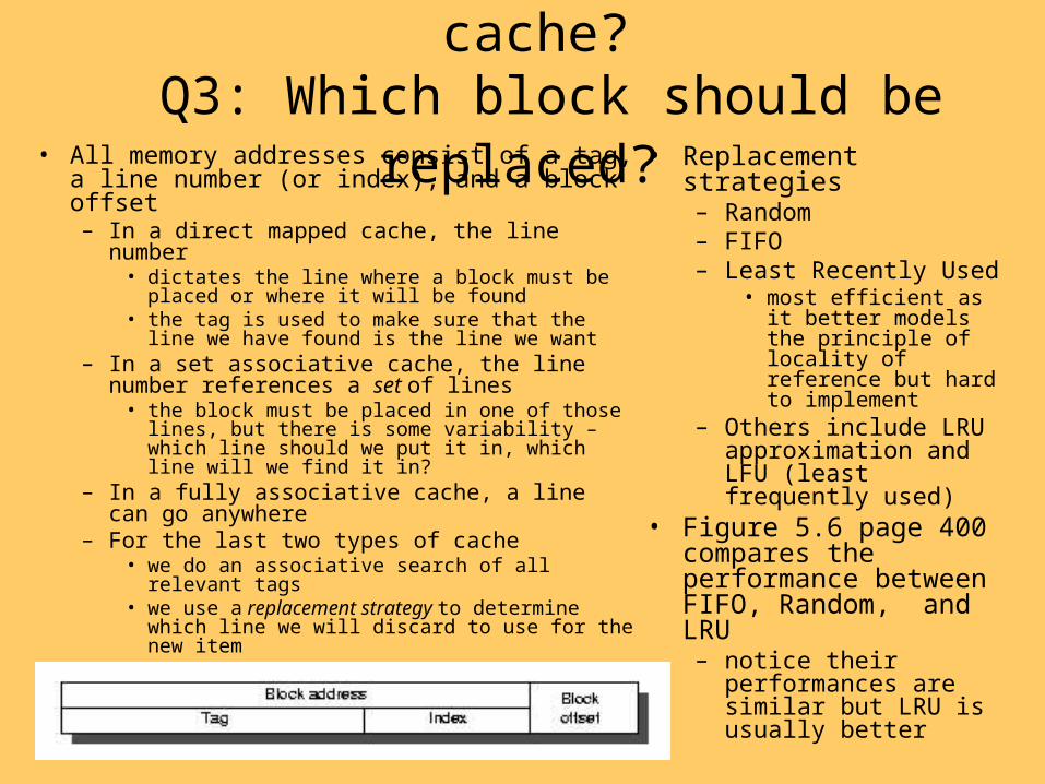
• All memory addresses consist of a tag, a line number (or index), and a block offset– In a direct mapped cache, the line number
• dictates the line where a block must be placed or where it will be found
• the tag is used to make sure that the line we have found is the line we want
– In a set associative cache, the line number references a set of lines
• the block must be placed in one of those lines, but there is some variability – which line should we put it in, which line will we find it in?
– In a fully associative cache, a line can go anywhere
– For the last two types of cache• we do an associative search of all relevant tags• we use a replacement strategy to determine which
line we will discard to use for the new item
• Replacement strategies– Random – FIFO– Least Recently Used
• most efficient as it better models the principle of locality of reference but hard to implement
– Others include LRU approximation and LFU (least frequently used)
• Figure 5.6 page 400 compares the performance between FIFO, Random, and LRU– notice their performances
are similar but LRU is usually better
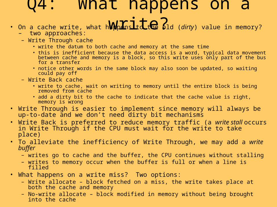
Q4: What happens on a write?• On a cache write, what happens to the old (dirty) value in memory? – two
approaches:– Write Through cache
• write the datum to both cache and memory at the same time• this is inefficient because the data access is a word, typical data movement between cache
and memory is a block, so this write uses only part of the bus for a transfer• notice other words in the same block may also soon be updated, so waiting could pay off
– Write Back cache• write to cache, wait on writing to memory until the entire block is being removed from
cache• add a dirty bit to the cache to indicate that the cache value is right, memory is wrong
• Write Through is easier to implement since memory will always be up-to-date and we don’t need dirty bit mechanisms
• Write Back is preferred to reduce memory traffic (a write stall occurs in Write Through if the CPU must wait for the write to take place)
• To alleviate the inefficiency of Write Through, we may add a write buffer – writes go to cache and the buffer, the CPU continues without stalling– writes to memory occur when the buffer is full or when a line is filled
• What happens on a write miss? Two options:– Write allocate – block fetched on a miss, the write takes place at both the cache and
memory– No-write allocate – block modified in memory without being brought into the cache
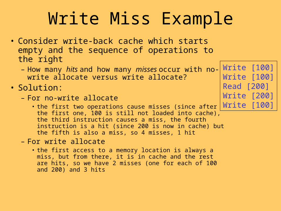
Write Miss Example• Consider write-back cache which starts empty and
the sequence of operations to the right– How many hits and how many misses occur with no-
write allocate versus write allocate?
• Solution:– For no-write allocate
• the first two operations cause misses (since after the first one, 100 is still not loaded into cache), the third instruction causes a miss, the fourth instruction is a hit (since 200 is now in cache) but the fifth is also a miss, so 4 misses, 1 hit
– For write allocate• the first access to a memory location is always a miss, but
from there, it is in cache and the rest are hits, so we have 2 misses (one for each of 100 and 200) and 3 hits
Write [100]Write [100]Read [200]Write [200]Write [100]
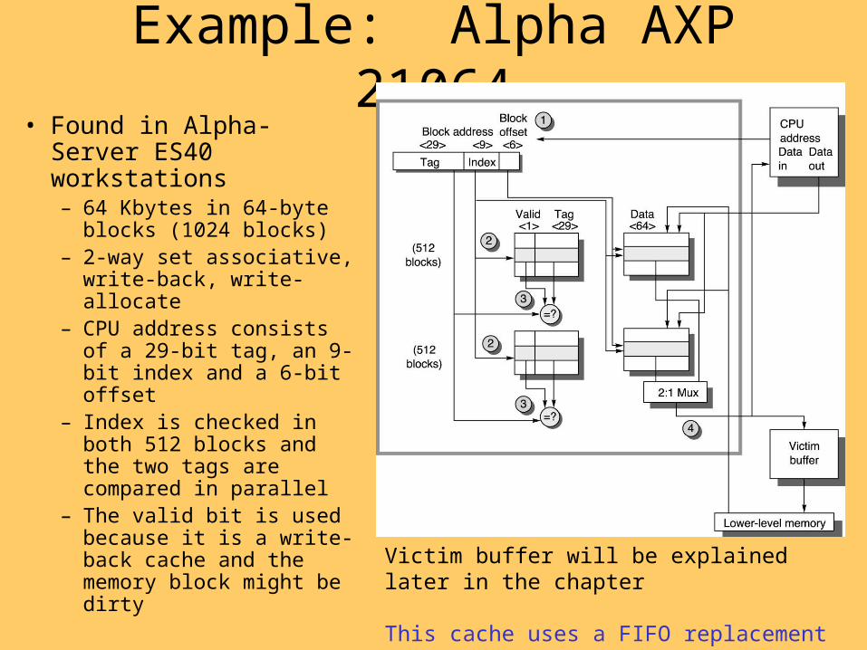
Example: Alpha AXP 21064• Found in Alpha-Server
ES40 workstations– 64 Kbytes in 64-byte
blocks (1024 blocks)– 2-way set associative,
write-back, write-allocate – CPU address consists of a
29-bit tag, an 9-bit index and a 6-bit offset
– Index is checked in both 512 blocks and the two tags are compared in parallel
– The valid bit is used because it is a write-back cache and the memory block might be dirty
Victim buffer will be explained later in the chapter
This cache uses a FIFO replacement strategy and transfers 16 bytes per cycle for 4 cycles on a miss
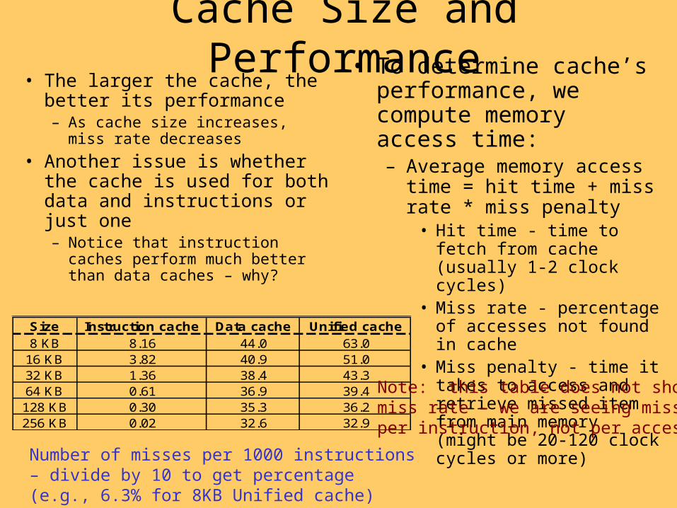
Cache Size and Performance• The larger the cache, the better its
performance– As cache size increases, miss rate
decreases
• Another issue is whether the cache is used for both data and instructions or just one– Notice that instruction caches
perform much better than data caches – why?
• To determine cache’s performance, we compute memory access time:– Average memory access time =
hit time + miss rate * miss penalty
• Hit time - time to fetch from cache (usually 1-2 clock cycles)
• Miss rate - percentage of accesses not found in cache
• Miss penalty - time it takes to access and retrieve missed item from main memory (might be 20-120 clock cycles or more)
Size Instruction cache Data cache Unified cache8 KB 8.16 44.0 63.0
16 KB 3.82 40.9 51.032 KB 1.36 38.4 43.364 KB 0.61 36.9 39.4128 KB 0.30 35.3 36.2256 KB 0.02 32.6 32.9
Number of misses per 1000 instructions – divide by 10 to get percentage (e.g., 6.3% for 8KB Unified cache)
Note: this table does not showmiss rate – we are seeing missesper instruction, not per access
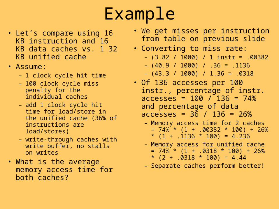
Example• Let’s compare using 16 KB
instruction and 16 KB data caches vs. 1 32 KB unified cache
• Assume: – 1 clock cycle hit time – 100 clock cycle miss penalty
for the individual caches– add 1 clock cycle hit time for
load/store in the unified cache (36% of instructions are load/stores)
– write-through caches with write buffer, no stalls on writes
• What is the average memory access time for both caches?
• We get misses per instruction from table on previous slide
• Converting to miss rate:– (3.82 / 1000) / 1 instr = .00382– (40.9 / 1000) / .36 = .1136– (43.3 / 1000) / 1.36 = .0318
• Of 136 accesses per 100 instr., percentage of instr. accesses = 100 / 136 = 74% and percentage of data accesses = 36 / 136 = 26%– Memory access time for 2 caches =
74% * (1 + .00382 * 100) + 26% * (1 + .1136 * 100) = 4.236
– Memory access for unified cache = 74% * (1 + .0318 * 100) + 26% * (2 + .0318 * 100) = 4.44
– Separate caches perform better!
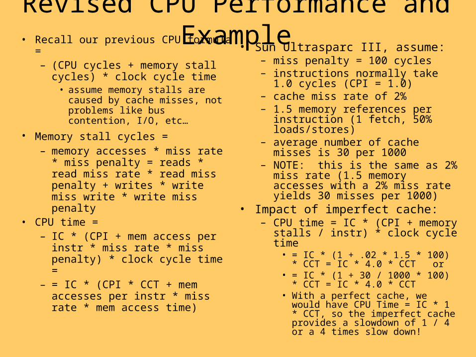
Revised CPU Performance and Example• Recall our previous CPU formula =
– (CPU cycles + memory stall cycles) * clock cycle time
• assume memory stalls are caused by cache misses, not problems like bus contention, I/O, etc…
• Memory stall cycles = – memory accesses * miss rate *
miss penalty = reads * read miss rate * read miss penalty + writes * write miss write * write miss penalty
• CPU time = – IC * (CPI + mem access per instr
* miss rate * miss penalty) * clock cycle time =
– = IC * (CPI * CCT + mem accesses per instr * miss rate * mem access time)
• Sun Ultrasparc III, assume:– miss penalty = 100 cycles– instructions normally take 1.0 cycles
(CPI = 1.0)– cache miss rate of 2% – 1.5 memory references per instruction
(1 fetch, 50% loads/stores)– average number of cache misses is 30
per 1000– NOTE: this is the same as 2% miss
rate (1.5 memory accesses with a 2% miss rate yields 30 misses per 1000)
• Impact of imperfect cache:– CPU time = IC * (CPI + memory
stalls / instr) * clock cycle time• = IC * (1 + .02 * 1.5 * 100) * CCT =
IC * 4.0 * CCT or• = IC * (1 + 30 / 1000 * 100) * CCT =
IC * 4.0 * CCT• With a perfect cache, we would have
CPU Time = IC * 1 * CCT, so the imperfect cache provides a slowdown of 1 / 4 or a 4 times slow down!
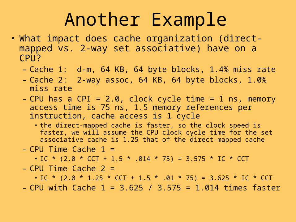
Another Example• What impact does cache organization (direct-mapped vs.
2-way set associative) have on a CPU?– Cache 1: d-m, 64 KB, 64 byte blocks, 1.4% miss rate– Cache 2: 2-way assoc, 64 KB, 64 byte blocks, 1.0% miss rate– CPU has a CPI = 2.0, clock cycle time = 1 ns, memory access
time is 75 ns, 1.5 memory references per instruction, cache access is 1 cycle
• the direct-mapped cache is faster, so the clock speed is faster, we will assume the CPU clock cycle time for the set associative cache is 1.25 that of the direct-mapped cache
– CPU Time Cache 1 = • IC * (2.0 * CCT + 1.5 * .014 * 75) = 3.575 * IC * CCT
– CPU Time Cache 2 = • IC * (2.0 * 1.25 * CCT + 1.5 * .01 * 75) = 3.625 * IC * CCT
– CPU with Cache 1 = 3.625 / 3.575 = 1.014 times faster
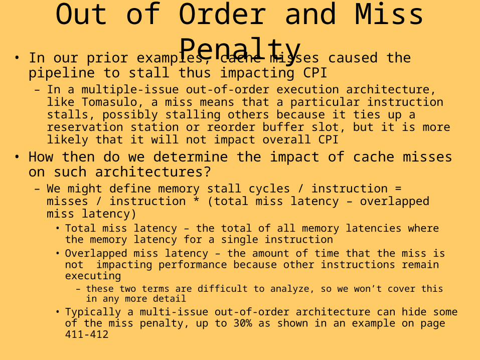
Out of Order and Miss Penalty• In our prior examples, cache misses caused the pipeline to stall
thus impacting CPI– In a multiple-issue out-of-order execution architecture, like Tomasulo, a
miss means that a particular instruction stalls, possibly stalling others because it ties up a reservation station or reorder buffer slot, but it is more likely that it will not impact overall CPI
• How then do we determine the impact of cache misses on such architectures?– We might define memory stall cycles / instruction = misses / instruction *
(total miss latency – overlapped miss latency)• Total miss latency – the total of all memory latencies where the memory
latency for a single instruction• Overlapped miss latency – the amount of time that the miss is not impacting
performance because other instructions remain executing– these two terms are difficult to analyze, so we won’t cover this in any more detail
• Typically a multi-issue out-of-order architecture can hide some of the miss penalty, up to 30% as shown in an example on page 411-412
Improving Cache Performance• After reading some 5000 research papers on caches, the
authors offer four distinct approaches to improving cache performance based on the formula:– average memory access time = hit time + miss rate * miss
penalty• Reduce miss rate• Reduce miss penalty• Reduce miss rate or miss penalty through parallelism• Reduce hit time
– For each of these, there are numerous possible approaches, many of them hardware or technology based, but a few can also be implemented by the compiler
• Comments:– miss penalty is the biggest value in the equation, so this should be the
obvious target to reduce, but in fact little can be done to increase memory speed
– reducing miss rate has a number of different approaches however miss rates today are often less than 2%, can we continue to improve?
– reducing hit time has the benefit of allowing us to lower clock cycle time as well
– We will look at each of these in sections 5.4-5.7
Reducing Cache Miss Penalties• Traditionally, the focus on cache improvements is on miss
rate– Since miss penalty is a large value, reducing it will have a large
impact on cache performance– Recall:
• average memory access time = hit time + miss rate * miss penalty• miss penalty is the time to retrieve from main memory
– A smaller miss penalty means that the miss rate has less of an impact
• The problem with reducing miss penalty is that– DRAM speeds stay roughly the same over time while processor
speed and SRAM access time increase dramatically• The net result is that the miss penalty has been increasing over time rather
than decreasing!
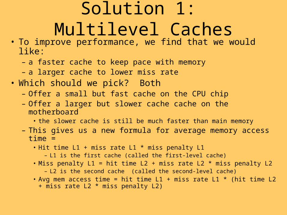
Solution 1: Multilevel Caches• To improve performance, we find that we would like:
– a faster cache to keep pace with memory – a larger cache to lower miss rate
• Which should we pick? Both– Offer a small but fast cache on the CPU chip– Offer a larger but slower cache cache on the motherboard
• the slower cache is still be much faster than main memory
– This gives us a new formula for average memory access time = • Hit time L1 + miss rate L1 * miss penalty L1
– L1 is the first cache (called the first-level cache)
• Miss penalty L1 = hit time L2 + miss rate L2 * miss penalty L2 – L2 is the second cache (called the second-level cache)
• Avg mem access time = hit time L1 + miss rate L1 * (hit time L2 + miss rate L2 * miss penalty L2)
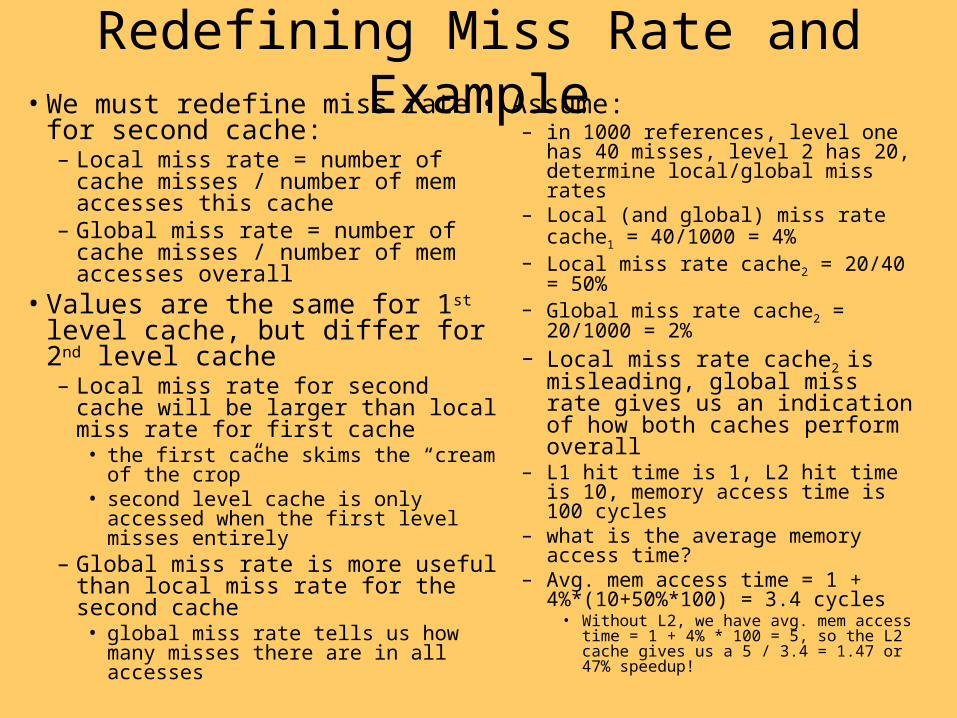
Redefining Miss Rate and Example• We must redefine miss rate for
second cache:– Local miss rate = number of cache
misses / number of mem accesses this cache
– Global miss rate = number of cache misses / number of mem accesses overall
• Values are the same for 1st level cache, but differ for 2nd level cache– Local miss rate for second cache will
be larger than local miss rate for first cache
• the first cache skims the “cream of the crop”
• second level cache is only accessed when the first level misses entirely
– Global miss rate is more useful than local miss rate for the second cache
• global miss rate tells us how many misses there are in all accesses
• Assume:– in 1000 references, level one has 40
misses, level 2 has 20, determine local/global miss rates
– Local (and global) miss rate cache1 = 40/1000 = 4%
– Local miss rate cache2 = 20/40 = 50%– Global miss rate cache2 = 20/1000 =
2%– Local miss rate cache2 is
misleading, global miss rate gives us an indication of how both caches perform overall
– L1 hit time is 1, L2 hit time is 10, memory access time is 100 cycles
– what is the average memory access time?
– Avg. mem access time = 1 + 4%*(10+50%*100) = 3.4 cycles
• Without L2, we have avg. mem access time = 1 + 4% * 100 = 5, so the L2 cache gives us a 5 / 3.4 = 1.47 or 47% speedup!
Another Example• Here we see the benefit of an associative cache for a
second-level cache instead of direct-mapped– Compare direct-mapped vs. 2-way set associative caches for
second level• Direct-mapped L2 has hit time = 10 cycles• Direct-mapped L2 has local miss rate = 25%• 2-way set-associative L2 has hit time = 10.1 cycles• 2-way set-associative L2 has local miss rate = 20%• Miss penalty L2 = 100 cycles
– Direct-mapped L2, miss penalty = 10 + .25 * 100 = 35 cycles– 2-way set-associative L2, miss penalty = 10.1 + .20 * 100 = 30.1
cycles• NOTE: we will almost always synchronize L2 with the clock, so in this
case, we would just raise the hit rate for the set-associative cache to be 11 cycles, resulting in a miss penalty = 11 + .20 * 100 = 31, still an improvement over direct-mapped
Solution 2: Early Restart• On a cache miss, memory system
moves a block into cache– moving a full block will require many
bus transfers
• Rather than having the cache (and CPU) wait until the entire block is available– move requested word from the block first
to allow cache access as soon as the item is available
• transfer rest of block in parallel with that access
– this requires two ideas:• early restart: the cache transmits the
requested word as soon as it arrives from memory
• critical word first: have memory return the requested word first and the remainder of the block afterward (this is also known as wrapped fetch)
• Example: calculate average memory access time for critical word and for the remainder of the block and compare against a cache that fetches the entire block without critical word first– 64-byte cache blocks– L2 takes 11 cycles to get first 8
bytes– 2 clock cycles per 8 bytes for the
remainder of the transfer– Avg. miss penalty = 11 cycles for
first word– Average miss penalty for entire
block = 11 + 2 * (64 – 8 ) / 8 = 25• To implement early restart/critical
word first, we need a non-block cache, this is expensive, so this approach only pays off if we have large block sizes (e.g., block size > bus bandwidth)

Solution 3: Priority of Reads over Writes• “Make the more common case fast”
– Reads occur with a much greater frequency than writes• instructions are read only, many operands are read but not written back
– So, lets make sure that reads are faster than writes• Writes are slower anyway because of the need to write to both cache and
main memory
– If we use a write buffer for both types of write policy:• Write-through cache writes to write buffer first, and any read misses are
given priority over writing the write buffer to memory
• Write-back cache writes to write buffer and the write buffer is only written to memory when we are assured of no conflict with a read miss
– So, read misses have priority over write misses since read misses are more common, so we make the common case fast
• See the example on pages 419-420
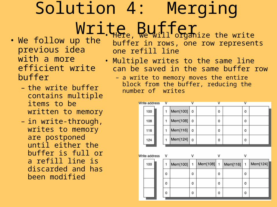
Solution 4: Merging Write Buffer• We follow up the
previous idea with a more efficient write buffer– the write buffer
contains multiple items to be written to memory
– in write-through, writes to memory are postponed until either the buffer is full or a refill line is discarded and has been modified
• Here, we will organize the write buffer in rows, one row represents one refill line
• Multiple writes to the same line can be saved in the same buffer row– a write to memory moves the entire block
from the buffer, reducing the number of writes

Solution 5: Victim Caches• Misses might arise when refill
lines conflict with each other – one line is discarded for another only
to find the discarded line is needed in the future
• The victim cache is a small, fully associative cache, placed between the cache and memory– this cache might store 1-5 blocks
• Victim cache only stores blocks that are discarded from the cache when a miss occurs– victim cache is checked on a miss
before going on to main memory and if found, the block in the cache and the block in the victim cache are switched
The victim cache is most useful if it backs up a fast direct-mapped cache to reduce the direct-mapped cache’s conflict miss rate by adding some associativity
A 4-item victim cache might remove ¼ of themisses from a 4KB direct-mapped data cache
AMD Athlon uses 8-entry victim cache
Reducing Cache Misses• Misses can be categorized as
– Compulsory • very first access to a block
cannot be in the cache because the process has just begun and there has not been a chance to load anything into the cache
– Capacity • the cache cannot contain all of
the blocks needed for the process
– Conflict • the block placement strategy
only allows a block to be placed in a certain location in the cache bringing about contention with other blocks for that same location
– See figure 5.14 page 424
• Compulsory miss rates are usually small – there is little we can do about
these misses other than prefetching
• We can eliminate all conflict misses if we – use a fully associative cache
• but fully associative caches are expensive in terms of hardware and slower which lengthens the clock cycle, reducing overall performance
• Little can be done for capacity misses – other than having larger caches
but we will find other things we can adjust to improve on capacity misses
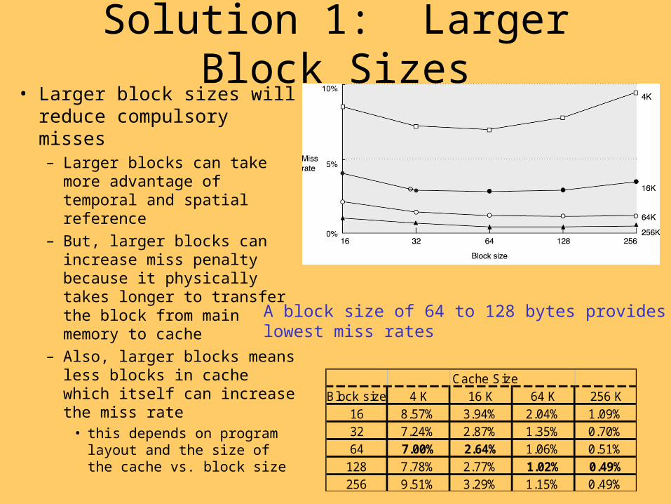
Solution 1: Larger Block Sizes• Larger block sizes will
reduce compulsory misses – Larger blocks can take more
advantage of temporal and spatial reference
– But, larger blocks can increase miss penalty because it physically takes longer to transfer the block from main memory to cache
– Also, larger blocks means less blocks in cache which itself can increase the miss rate
• this depends on program layout and the size of the cache vs. block size
A block size of 64 to 128 bytes provides thelowest miss rates
Cache SizeBlock size 4 K 16 K 64 K 256 K
16 8.57% 3.94% 2.04% 1.09%32 7.24% 2.87% 1.35% 0.70%64 7.00% 2.64% 1.06% 0.51%
128 7.78% 2.77% 1.02% 0.49%256 9.51% 3.29% 1.15% 0.49%
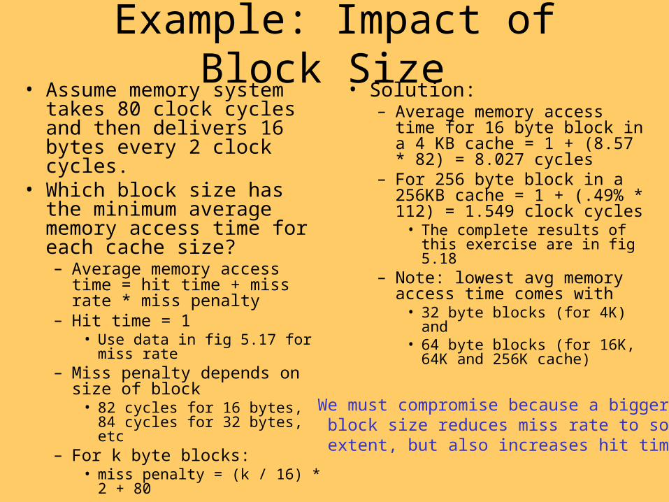
Example: Impact of Block Size • Assume memory system takes
80 clock cycles and then delivers 16 bytes every 2 clock cycles.
• Which block size has the minimum average memory access time for each cache size?– Average memory access time =
hit time + miss rate * miss penalty
– Hit time = 1• Use data in fig 5.17 for miss rate
– Miss penalty depends on size of block
• 82 cycles for 16 bytes, 84 cycles for 32 bytes, etc
– For k byte blocks: • miss penalty = (k / 16) * 2 + 80
• Solution:– Average memory access time for
16 byte block in a 4 KB cache = 1 + (8.57 * 82) = 8.027 cycles
– For 256 byte block in a 256KB cache = 1 + (.49% * 112) = 1.549 clock cycles
• The complete results of this exercise are in fig 5.18
– Note: lowest avg memory access time comes with
• 32 byte blocks (for 4K) and • 64 byte blocks (for 16K, 64K
and 256K cache)
We must compromise because a bigger block size reduces miss rate to some extent, but also increases hit time

Solution 2: Larger Caches• A larger cache will reduce capacity miss rates since the
cache has a larger capacity, but also conflict miss rates because the larger cache allows more refill lines and so fewer conflicts
• This is an obvious solution and has no seeming performance drawbacks– However, you must be careful where you put this larger
cache• A larger on-chip cache might take space away from other hardware
that could provide performance increases (registers, more functional units, logic for multiple-issue of instructions, etc)
– And more cache means a greater expense for the machine– The authors note that second-level caches from 2001
computers are equal in size to main memories from 10 years ago!
Solution 3: Higher Associativity• A large 8-way
associative cache will have about a 0% conflict miss rate meaning that they are about as good at reducing miss rate as fully associative caches
• Cache research also points out the “2:1 cache rule of thumb” – a direct-mapped cache of
size N has about the same miss rate as a 2-way set associative cache of size N/2 so that larger associativity yields smaller miss rates
• So why use direct-mapped? – associativity will always have a higher
hit time
• How big is the difference?– As we saw in an earlier example, a 2-
way set associative cache was about 10% slower than the direct-mapped
– This doesn’t seem like a big deal
• BUT– Clock speed is usually equal to cache
hit time so we wind up slowing down the entire computer when using associative caches of some kind
• So, with this in mind, should we use direct-mapped or set associative?
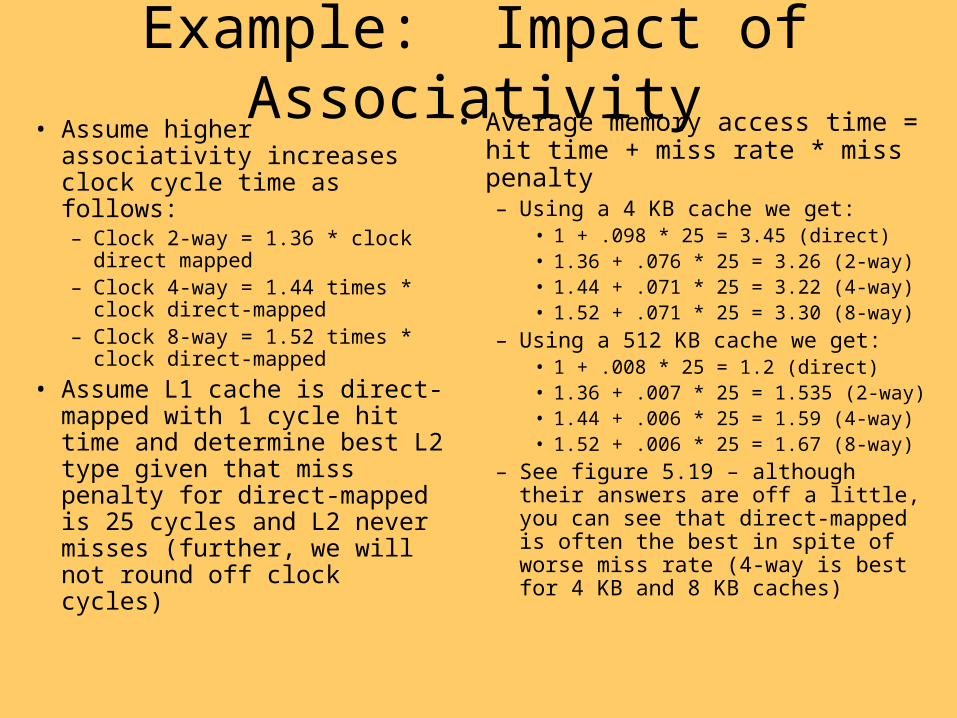
Example: Impact of Associativity• Assume higher associativity
increases clock cycle time as follows:– Clock 2-way = 1.36 * clock
direct mapped– Clock 4-way = 1.44 times *
clock direct-mapped– Clock 8-way = 1.52 times *
clock direct-mapped
• Assume L1 cache is direct-mapped with 1 cycle hit time and determine best L2 type given that miss penalty for direct-mapped is 25 cycles and L2 never misses (further, we will not round off clock cycles)
• Average memory access time = hit time + miss rate * miss penalty– Using a 4 KB cache we get:
• 1 + .098 * 25 = 3.45 (direct)• 1.36 + .076 * 25 = 3.26 (2-way)• 1.44 + .071 * 25 = 3.22 (4-way)• 1.52 + .071 * 25 = 3.30 (8-way)
– Using a 512 KB cache we get:• 1 + .008 * 25 = 1.2 (direct)• 1.36 + .007 * 25 = 1.535 (2-way)• 1.44 + .006 * 25 = 1.59 (4-way)• 1.52 + .006 * 25 = 1.67 (8-way)
– See figure 5.19 – although their answers are off a little, you can see that direct-mapped is often the best in spite of worse miss rate (4-way is best for 4 KB and 8 KB caches)
Solution 4: Pseudo-Associative Cache• We can alter a direct-mapped cache to have some
associativity as follows:– Consult the direct-mapped cache as normal
• provides fast hit time
– If there is a miss, invert the address and try the new address• inversion might flip the last bit in the line number• the second access comes at a cost of a higher hit rate for a second attempt
(it may also cause other accesses to stall while the second access is being performed!)
– Thus, the same address might be stored in one of two locations, thus giving some associativity
– The pseudo-associative cache will reduce the amount of conflict misses
• any cache miss may still become a cache hit
– First check is fast (hit time of direct-mapped)– Second check might take 1-2 cycles further, so is still faster than
a second-level cache
Example• Assume hit time = 1 cycle for 1st access, 3 cycles for
2nd access and a miss penalty of 50 cycles• Which provides a faster average memory access time
for 4KB and 256 KB caches, direct-mapped, 2-way associative or pseudo-associative (PAC)?– avg mem acc time = hit time + miss rate * miss penalty
• For PAC, an entry will either be in its direct-mapped location or the location found by inverting 1 bit
– since each entry in the PAC has 2 possible locations, this makes the PAC similar to a 2-way associative cache, but the PAC has a faster first hit time than 2-way associative, followed by a second access (in this case, 3 cycles)
– avg mem access time = hit time + alternative hit rate * 3 + miss rate2 way * miss penalty1 way
• Alternative hit rate is hit rate for the second access– with 2 possible places for the item, this second hit rate will be
hit rate2 way - hit rate1 way – that is, the hit rate of a 2-way set associative cache (because there are 2 places the item could be placed) – the hit rate of a direct-mapped cache
• Alternative hit rate = hit rate2 way - hit rate1 way = 1 - miss rate2 way - (1 - miss rate1 way) = miss rate1 way - miss rate2 way
• For PAC:– 4 KB = 1 + (.098
- .076) * 3 + (.076 * 50) = 4.866
– 256 KB = 1 + (.013 - .012) * 3 + (.012 * 50) = 1.603
• For direct-mapped cache:
– For 4 KB = 1 + .098 * 50 = 5.9
– For 256 KB = 1 + .013 * 50 = 1.65
• For 2-way set associative (recall, longer clock cycle):
– For 4 KB = 1.36 + .076 * 50 = 5.16
– For 256 KB = 1.36 + .012 * 50 = 1.96
• So, pseudo-associative cache outperforms both!
Solution 5: Compiler Optimizations• We have already
seen that compiler optimizations can be used to improve hardware performance
• What about using compiler optimizations to improve cache performance?– It turns that that there
are numerous things we can do
• For specific examples, see pages 432-434
• Specific techniques include:– merging parallel arrays into an array of
records so that access to a single array element is made to consecutive memory locations and thus the same (hopefully) refill line
– loop interchange exchange loops in a nested loop situation so that array elements are accessed based on order that they will appear in the cache and not programmer-prescribed order
– Loop fusion combines loops together that access the same array locations so that all accesses are made within one iteration
– Blocking executes code on a part of the array before moving on to another part of the array so that array elements do not need to be reloaded into the cache
• This is common for applications like image processing where several different passes through a matrix are made
Using Parallelism for Reduction• Other techniques to reduce miss penalty and/or rate utilize
parallelism– A non-blocking cache allows a cache to continue to handle
accesses even after a cache miss results in a memory request• Non-blocking caches are needed for out-of-order execution architectures and
for allowing critical word first to work (if the cache was blocked, the first word received would not be available until the entire block was received)
– Non-blocking caches are expensive even though they can be very useful
– Two additional ideas that use non-blocking caches are:• Hardware prefetching to fetch multiple blocks when a miss is made (that is,
hardware predicts what else should be retrieved from memory) – See pages 438-439 for an example
• Compiler-controlled prefetching whereby the compiler places prefetching commands in the program so that data are loaded into the cache before they are needed (reducing compulsory miss rate)
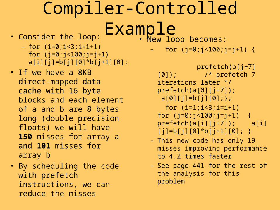
Compiler-Controlled Example• Consider the loop:
– for (i=0;i<3;i=i+1)for
(j=0;j<100;j=j+1) a[i][j]=b[j][0]*b[j+1][0];
• If we have a 8KB direct-mapped data cache with 16 byte blocks and each element of a and b are 8 bytes long (double precision floats) we will have 150 misses for array a and 101 misses for array b
• By scheduling the code with prefetch instructions, we can reduce the misses
• New loop becomes:– for (j=0;j<100;j=j+1) {
prefetch(b[j+7][0]); /* prefetch 7 iterations later */ prefetch(a[0][j+7]); a[0][j]=b[j][0];};
for (i=1;i<3;i=i+1) for (j=0;j<100;j=j+1) {
prefetch(a[i][j+7]); a[i][j]=b[j][0]*b[j+1][0]; }
– This new code has only 19 misses improving performance to 4.2 times faster
– See page 441 for the rest of the analysis for this problem
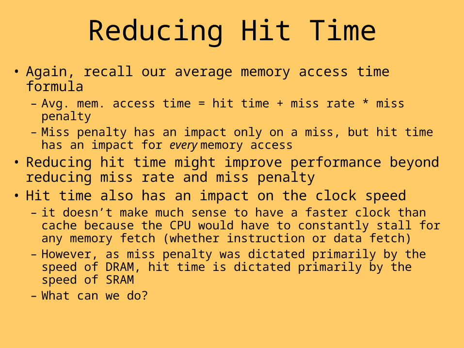
Reducing Hit Time• Again, recall our average memory access time formula
– Avg. mem. access time = hit time + miss rate * miss penalty– Miss penalty has an impact only on a miss, but hit time has an
impact for every memory access
• Reducing hit time might improve performance beyond reducing miss rate and miss penalty
• Hit time also has an impact on the clock speed – it doesn’t make much sense to have a faster clock than cache
because the CPU would have to constantly stall for any memory fetch (whether instruction or data fetch)
– However, as miss penalty was dictated primarily by the speed of DRAM, hit time is dictated primarily by the speed of SRAM
– What can we do?
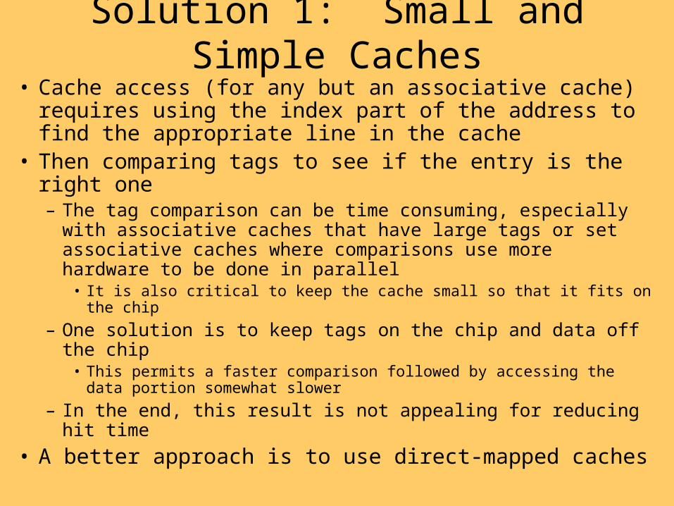
Solution 1: Small and Simple Caches
• Cache access (for any but an associative cache) requires using the index part of the address to find the appropriate line in the cache
• Then comparing tags to see if the entry is the right one– The tag comparison can be time consuming, especially with
associative caches that have large tags or set associative caches where comparisons use more hardware to be done in parallel
• It is also critical to keep the cache small so that it fits on the chip
– One solution is to keep tags on the chip and data off the chip • This permits a faster comparison followed by accessing the data portion
somewhat slower
– In the end, this result is not appealing for reducing hit time
• A better approach is to use direct-mapped caches
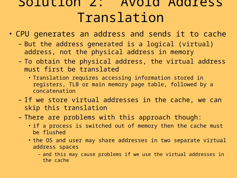
Solution 2: Avoid Address Translation
• CPU generates an address and sends it to cache– But the address generated is a logical (virtual) address, not the
physical address in memory
– To obtain the physical address, the virtual address must first be translated
• Translation requires accessing information stored in registers, TLB or main memory page table, followed by a concatenation
– If we store virtual addresses in the cache, we can skip this translation
– There are problems with this approach though:• if a process is switched out of memory then the cache must be flushed
• the OS and user may share addresses in two separate virtual address spaces
– and this may cause problems if we use the virtual addresses in the cache

Solution 3: Pipelining Writes • Writes will take longer than reads because the tag must
be checked before the write can begin – A read can commence and if the tag is wrong, the item read
can be discarded– The write takes two steps, tag comparison first, followed by
the write (a third step might be included in a write-back cache by combining items in a buffer)
– By pipelining writes• we can partially speed up the process
– This works by overlapping the tag checking and writing portions
• assuming the tag is correct• in this way, the second write takes the same time as a read would
– although this only works with more than 1 consecutive write where all writes are cache hits
Solution 4: Trace Caches• This type of a cache is an instruction cache which
supports multiple issue of instructions by providing 4 or more independent instructions per cycle– Cache blocks are dynamic, unlike normal caches where blocks
are static based on what is stored in memory– Here, the block is formed around branch prediction, branch
folding, and trace scheduling (from chapter 4)– Note that because of branch folding and trace scheduling, some
instructions might appear multiple times in the cache, so it is somewhat more wasteful of cache space
• This type of cache then offers the advantage of directly supporting a multiple issue architecture– The Pentium 4 uses this approach, but most RISC computers
do not because repetition of instructions and high frequency of branches cause this approach to waste too much cache space
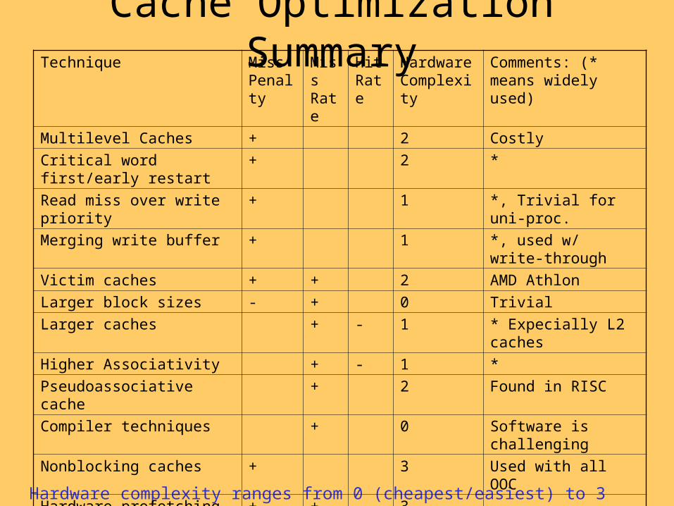
Cache Optimization Summary
Hardware complexity ranges from 0 (cheapest/easiest) to 3 (most expensive/hardest)
Technique Miss Penalty
Miss Rate
Hit Rate
Hardware Complexity
Comments: (* means widely used)
Multilevel Caches + 2 Costly
Critical word first/early restart + 2 *
Read miss over write priority + 1 *, Trivial for uni-proc.
Merging write buffer + 1 *, used w/ write-through
Victim caches + + 2 AMD Athlon
Larger block sizes - + 0 Trivial
Larger caches + - 1 * Expecially L2 caches
Higher Associativity + - 1 *
Pseudoassociative cache + 2 Found in RISC
Compiler techniques + 0 Software is challenging
Nonblocking caches + 3 Used with all OOC
Hardware prefetching + + 3
Compiler prefetching + + 3
Small/simple caches - + 0 *, trivial
No address translation + 2 Trivial if small cache
Pipelining writes + 1 *
Trace cache + 3 Used in P4

![Chapter 21 Cache - National Tsing Hua Universityoz.nthu.edu.tw/~d947207/chap21_cache.pdf · Chapter 21 Cache Speaker: Lung-Sheng Chien Reference: [1] David A. Patterson and John L.](https://static.fdocuments.in/doc/165x107/5f0679157e708231d4182adc/chapter-21-cache-national-tsing-hua-d947207chap21cachepdf-chapter-21-cache.jpg)