CHAPTER 5 A NEW SPACE VECTOR TECHNIQUE...
32
121 CHAPTER 5 A NEW SPACE VECTOR TECHNIQUE FOR THE DIRECT THREE-LEVEL MATRIX CONVERTER 5.1 INTRODUCTION The voltage stresses on the power devices can be reduced by using multi-level inverters (MLIs) (Celanovic and Boroyevich 2000, Lopez et al 2008 and Aneesh et al 2009). MLIs permit the use of lower rating power supplies and power devices for achieving higher output power rating. Using the same idea in the matrix converters, a new family of converters called multilevel matrix converters evolved with different concepts: i) Replacing each bidirectional switch in the CMC with n cells, each cell consisting of a capacitor connected to the centre of the H Bridge (Erickson and Al-Naseem 2001 and Erickson et al 2006). This topology generates multi-level output but at the cost of a more complicated circuit configuration and modulation strategy. ii) Modifying the topology of the IMC with additional switches, which makes available two different voltages levels at the output, i.e., the phase and the line voltages (Meng Yeong Lee et al 2010). This topology is effective for two-level and three-level voltage conversion with less complicated circuit configuration and modulation strategy as compared to (i). Modified IMC based three-level converter uses the diode clamped multi-level space vector technique (Meng Yeong Lee et al 2010) on the inverter side and the conventional space vector technique on the rectifier side. In this chapter, a new class of direct three-level matrix converter (DTMC) along with its modulation techniques is developed and its performance is analyzed.
Transcript of CHAPTER 5 A NEW SPACE VECTOR TECHNIQUE...

121
CHAPTER 5
A NEW SPACE VECTOR TECHNIQUE FOR THE DIRECT
THREE-LEVEL MATRIX CONVERTER
5.1 INTRODUCTION
The voltage stresses on the power devices can be reduced by using
multi-level inverters (MLIs) (Celanovic and Boroyevich 2000, Lopez et al
2008 and Aneesh et al 2009). MLIs permit the use of lower rating power
supplies and power devices for achieving higher output power rating. Using
the same idea in the matrix converters, a new family of converters called
multilevel matrix converters evolved with different concepts: i) Replacing
each bidirectional switch in the CMC with n cells, each cell consisting of a
capacitor connected to the centre of the H Bridge (Erickson and Al-Naseem
2001 and Erickson et al 2006). This topology generates multi-level output but
at the cost of a more complicated circuit configuration and modulation
strategy. ii) Modifying the topology of the IMC with additional switches,
which makes available two different voltages levels at the output, i.e., the
phase and the line voltages (Meng Yeong Lee et al 2010). This topology is
effective for two-level and three-level voltage conversion with less complicated circuit configuration and modulation strategy as compared to (i).
Modified IMC based three-level converter uses the diode clamped
multi-level space vector technique (Meng Yeong Lee et al 2010) on the
inverter side and the conventional space vector technique on the rectifier side.
In this chapter, a new class of direct three-level matrix converter (DTMC)
along with its modulation techniques is developed and its performance is analyzed.
122
5.2 PROBLEM FORMULATION
The objective of this chapter is to develop a new DTMC topology
namely, the direct three-level matrix converter, which requires three
bidirectional switches of lower ratings (phase voltage rated) and the CMC
topology. The structure is a 4 × 3 matrix converter that facilitates the increase
in the output voltage levels by making the source neutral available to the load
terminals. In addition to the multilevel operation, the converter also has the
ability to control bi-directional power flow. The proposed DTMC is evaluated
by simulation and hardware experimentation. The modulation strategy of the
DTMC uses the multi-level space vector modulation technique along with the
proposed neutral current balancing strategy. The same is implemented using
the Xilinx based system generator facility, which is available as a toolbox in
MATLAB R2010a, along with an FPGA.
5.3 PROPOSED TOPOLOGY
A DTMC in its very generic form, shown in Figure 5.1, consists of
three arms that are connected to the source and one arm connected to the star
point (neutral) of the input filter capacitances. Figure 5.1 depicts the general
configuration of the proposed DTMC structure which consists of a CMC and
a neutral point connecter.
5.3.1 Indirect Matrix Converter Representation for the DTMC
The proposed DTMC topology consists of an array of 4 × 3 bi-
directional switches, which includes the 3 × 3 switches of the CMC and three
additional switches for making the neutral point of the input filter capacitance
to be available at the load terminals. Equations (5.1) and (5.2) give the output
voltages and the input currents of the DTMC.

123
Figure 5.1 Topology of the direct three-level matrix converter
VaVbVc
=SAa SBa SCaSAb SBb SCbSAc SBc SCc
SNaSNbSNc
×
VAVBVC0
(5.1)
IAIBICIN
=
SAa SAb SAcSBa SBb SBcSCa SCb SCcSNa SNb SNc
×IaIbIc
(5.2)
Since the DTMC is supplied by a voltage source, the input phases
must never be shorted, and due to the inductive nature of the load, the output
phases must never be left open. These constraints are realized by
Equation (5.3).
SAj+SBj+SCj+SNj=1 j {a,b,c} (5.3)
VA
VB
Va Vb
VC
Vc
SAa
SBa
SCa SCb SCc
SBb SBc
SAb SAc
Ia Ib Ic
IA
IB
IC
IN
SNa SNb SNc

124
The DTMC can be decoupled into an indirect three-level matrix
converter (ITMC) consisting of a fictitious two-level converter (FTC – input
converter) and a fictitious inverter (FI - output converter), as shown in
Figure 5.2.
Figure 5.2 Topology of the indirect three-level matrix converter
The FTC consists of three phase arms and one neutral arm.
Switching ON any of the two phase arms leads to the line voltage being
available at the FDCB and switching ON any one phase arm with the neutral
arm leads to the phase voltage being available at the FDCB. This results in
twelve active voltage vectors on the rectifier side. This decoupled
representation simplifies the control of the input current and the output
voltage in DTMC, as described in the next section.
Vc
Vb
Va
VDC+
SIA SIB SIC
SIa SIb SIc
SCA SCB SCC
SCa SCb SCc
IA
IB
IC
Ic
Ib
IaVDC
VA
VB
VC
VDC-Rectifier part (FTC)
Inverter part (FI)
SCn
SCN
IDC+
IDC-
INVN

125
5.4 SPACE VECTOR MODULATION TECHNIQUE FOR THE
DTMC
The switching function for the DTMC is represented as the product
of the rectifier switching function and the inverter switching function and is
given by Equation (5.4).
SAa SBa SCaSAb SBb SCbSAc SBc SCc
SNaSNbSNc
=SIA SIaSIB SIbSIC SIc
×SCA SCB SCCSCa SCb SCc
SCN SCn
(5.4)
The switching states for synthesizing the required currents and
voltages are described in the following subsections.
5.4.1 The Fictitious Two-Level Converter Stage
Assuming that the output of the FTC is a constant current source
IDC, the space vector for all valid switching states are determined by
Equations (5.5) to (5.7).
I = IA + IB cos3
+ IC cos3
(5.5)
I = IB sin3
+ IC sin3
(5.6)
I0 = IA + IB + IC (5.7)
As described in Section 5.3.1, switching ON the neutral arm causes
the current to flow in the source neutral resulting in the space vector having a
component along the I0 axis. Table 5.1 gives the space vector components for
different valid switching states and Figure 5.3(a) shows the space vectors
distribution

126
Table 5.1 Space vectors for the fictitious two-level converter
Type Vector
SCASCa
SCBSCb
SCCSCc
SCNSCn
IA IB IC IN=I0 IinA
ctiv
elo
ngve
ctor
s
IL1[AB] 10
0100
00 +IDC -IDC 0 0 3IDC 3300 VAB
IL2[AC] 10
0001
00 +IDC 0 -IDC 0 3IDC 300 VAC
IL3[BC] 00
0010
01
0 +IDC -IDC 0 3IDC 900 VBC
IL4[BA] 01
1000
00
-IDC +IDC 0 0 3IDC 1500 VBA
IL5[CA] 01
0010
00 -IDC 0 +IDC 0 3IDC 2100 VCA
IL6[CB] 00
0110
00
0 -IDC +IDC 0 3IDC 2700 VCB
Act
ive
shor
tve
ctor
s
IP1[AN] 10
0000
01 +IDC 0 0 -IDC IDC 00 VAN
IP2[NC] 00
0001
10
0 0 -IDC +IDC IDC 600 VNC
IP3[BN] 00
1000
01
0 +IDC 0 -IDC IDC 1200 VBN
IP4[NA] 01
0000
10 -IDC 0 0 +IDC IDC 1800 VNA
IP5[CN] 00
0010
01
0 0 +IDC -IDC IDC 2400 VCN
IP6[NB] 00
0100
10 0 -IDC 0 +IDC IDC 3000 VNB
Zero
vect
ors
IZ
1 0 01 0 0
00
0 1 00 1 0
00
0 0 10 0 1
00
0 0 00 0 0
11
0 0
where, Iin= I 2+I 2 and Iin= tan-1 I
I .
Vectors represented by ILi (active long vectors) are conventional
rectifier space vectors, which do not contribute to the neutral current. Vectors
represented by IPi (active short vectors) contribute to the neutral current. To
ensure that the input current is sinusoidal, the reference space vector must lie
on the plane requiring the neutral current to be zero on application of the
vector IPi. This is carried out by applying equally the adjacent IPi vectors,

127
which lie on the upper and the lower halves of the plane. This ensures that
the average neutral current is zero over a switching period. The example in
Table 5.2 explains the same.
Table 5.2 Neutral current balancing and virtual vector synthesis
Switching time Applied vectors IA IB IC IN VDC
Ts
2IP6 0 -IDC 0 +IDC VNB
Ts
2IP1 +IDC 0 0 -IDC VAN
Ts IVP1=12
IP6+12
IP1 +12
IDC -12
IDC 0 012
VAB
This solution to the neutral current balancing problem (Celanovic
and Boroyevich 2000) introduces virtual vectors IVPi, which lie completely on
the plane, as given in Table 5.3 and shown in Figure 5.3(b).
Figure 5.3(a) Space vectors of the FTC
IP2
IL3
IP5
IP3 IP1
IP6
IP4
IZ1, IZ2, IZ3, IZ4
IL6IL5
IL4
IL2
IL1

128
Figure 5.3(b) Space vectors and virtual vectors of the FTC
Table 5.3 Virtual current space vectors
Virtual vectors
Sharing vectors
IA IB ICIN =I0
Iin Iin VDC
IVP1[AN] IP6,IP1 +12
IDC -12
IDC 0 0 32
IDC 3300 12
VAB
IVP2[NC] IP1,IP2 +12
IDC 0 -12
IDC 0 32
IDC 300 12
VAC
IVP3[BN] IP2,IP3 0 +12
IDC -12
IDC 0 32
IDC 900 12
VBC
IVP4[NA] IP3,IP4 -12
IDC +12
IDC 0 0 32
IDC 1500 12
VBA
IVP5[CN] IP4,IP5 -12
IDC 0 +12
IDC 0 32
IDC 2100 12
VCA
IVP6[NB] IP5,IP6 0 -12
IDC +12
IDC 0 32
IDC 2700 12
VCB
IVP6
IVP5
IVP4
IVP3
IVP2
IVP1
IP4
IP6
IP1
IP5
IP2IP3
IL6
IL5
IL4
IL3
IL2
IL1
3
5
1
4
2
0

129
Figure 5.4(a) shows the sector zero of the space vector diagram of
the FTC. Each sector consists of two active long vectors, two active virtual
short vectors and four zero vectors. To synthesize the required reference input
current and the FDCB voltage, the three nearest current vectors (Busquets-
Monge et al 2004) are selected, as shown in Figure 5.4(b), depending on the
modulation index mc of the FTC.
Figure 5.4(a) Sector region identification of the FTC
Figure 5.4(b) Region vector identification of the FTC
In order to identify the region in which the reference vector lies,
equations of the three lines are derived and shown in Figure 5.5. Table 5.4
gives the rules for identifying the region in which the reference vector lies in
the FTC for different values of modulation indices mc.
I3
I1
I2
E
G
F
H
R4
B I3
I2
I1
I3F
B
I2
A I1 R5DH
C
E
B
R1
F
H D
C
E
I2
I1
I3
R3
C
B
G
F
H
I2
I1
I3 R2
C
IREF
HG
FE
IL1 C
IZ
AD
R3
R4R2
R1
IL2
IVP2
IVP1
R5
B

130
34
cosec 600c ; 00
c<600
12
sec 600c ; 300
c<600
12
sec( c) ; 00c<300
Figure 5.5 Equations of lines used for identifying regions in the FTC
Table 5.4 Region identification for a given IREF
Conditions
1 R1 mc>12
sec( c) ; 00c<300
2 R2 mc>12
sec 600c ; 300
c<600
3 R33
4cosec 600
c <mc12
sec( c) ; 00c<300
4 R43
4cosec 600
c <mc12
sec 600c ; 300
c<600
5 R5 mc3
4cosec 600
c ;00c<600
Duty cycles of the selected vectors for different regions are
computed using Equation (5.8), where (xi, yi) are the coordinates of the
selected vector Ii and di is its duty cycle. X and Y are the coordinates of the
reference vector IREF and are given by Equation (5.9).
C
IREF
IL1
IZ
IVP2
IVP1
IL2
1/ 3
1/2
1/2
1
1
3/4 3/2

131
x1 x2 x3y1 y2 y31 1 1
d1d2d3
=XY1
(5.8)
X = mc × cos c & Y = mc × sin c (5.9)
While computing the duty cycle, the sector in Figure 5.6(a) is
rotated as shown in Figure 5.6 (b). The coordinates are chosen according to
the region in which the reference vector lies, as shown in Figure 5.6 (b).
Table 5.5 gives the duty cycles derived for different regions
Figure 5.6 (a) Sector 1 and (b) sector 1 rotated
Table 5.5 Duty cycles for different regions in a given sector
Duty Cycle
d1- I1 d2- I2 d3 - I3
R123
mc sin( c) 2 mc cos( c) -1 2 - 43
mc sin 600c
R2 2 mc sin 300c -1
23
mc sin 600c 2 -
43
mc sin 600c
R343
mc sin 600c -1
43
mc sin 600c 2 - 4 mc cos( c)
R443
mc sin 600c -1 2 - 4 mc sin 300
c43
mc sin c
R5 1 - 43
mc sin 600c
43
mc sin 600c
43
mc sin c
C
IREF(mccos c, mcsin c)
IL1(1, 0)IZ(0, 0)
IL2( cos600, sin600)
IVP2 (0.5 cos600, 0.5 sin600)
IVP1(0.5, 0)X
Y
C
IREF
IL1
IZ
IL2
IVP2
IVP1
X
Y

132
where, c is the angle of IREF within the sector and mc is the inverter zero
compensated converter modulation index discussed later and is given in
Equation (5.14).
5.4.2 The Fictitious Inverter Stage
The conventional SVPWM is implemented in the inverter stage.
This consists of six active voltage vectors and two zero voltage vectors, as
shown in Figure 5.7. To generate the required reference vector VOUT, adjacent
active vectors V , V and a zero vector V0 are selected whose duty cycles d , d
and d0 are given by Equation (5.10)
d = sin 600v , d = sin( v) and d0 = 1- (d +d ) (5.10)
where, v is the angle of VOUT within a sector. The output voltage of the
inverter can be adjusted by any one of the two schemes: (i) changing the
FDCB voltage to the inverter, (ii) changing the modulation index mv of the
inverter. The second scheme is not used for reasons explained in the next
paragraph and hence mv=1. The FDCB voltage can be varied by changing the
modulation index mc' of FTC as given in Equation (5.11)
Figure 5.7 (a) Space vectors of the FI and (b) sector and duty cycle allocation
V0 d0V d
V dVREF
V
V
v
V2 [110] VMe /3
V4 [011] VMe V d
Vd
1
vV1 [100] VMe-j0
V6 [101] VMe-j /3
V5 [001] VMe-j2 /3
V3 [010] VMej2 /3
Vc
Va
05
4
3
2
Vb
VOUT
Zero VectorsV0 [000]V7 [111]

133
mc' = 3
2mDTMC (5.11)
where, mDTMC is the required modulation index of the DTMC. At higher
modulation indices, the FTC reference vector, Iin, lies in any one of the
regions R1, R2, R3 or R4. These regions do not use any zero vectors for the
modulation, as described in section 5.4.1. Simultaneous use of the zero
vectors at the inverter stage would cause the output voltage to become zero.
This is not consistent with the idea of multilevel switching techniques as it
increases the THD at the output. To decrease the THD of the DTMC, zero
vectors are not used at the inverter stage, which does not allow for the change
in modulation index mv. With the elimination of the zero vectors, the duty
cycles for active vectors are recomputed as given in Equation (5.12). This
increases the output voltage vector as given by Equation (5.13).Thus the
reference vector is brought outside the inscribed circle of the space vector
hexagon leading to an over modulation condition.
d' = d
d + d & d' = d
d + d (5.12)
VOUT' = d' V + d' V = VOUT
d + d (5.13)
The increase in the output voltage vector is compensated by
adjusting the FDCB voltage by modifying the modulation index of the FTC
dynamically, as given by Equation (5.14).
mc= 32
mDTMC d +d (5.14)
Figure 5.8 shows the allocation of the switching vectors in a
sampling period for a particular inverter sector and for different regions of the
converter sector. The period of the virtual vector is divided into two, during
which the adjacent upper and lower active short vectors of the corresponding
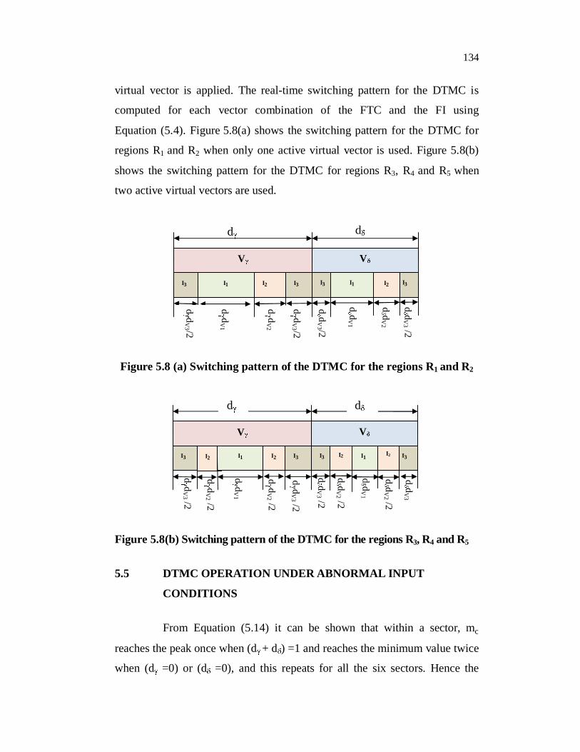
134
virtual vector is applied. The real-time switching pattern for the DTMC is
computed for each vector combination of the FTC and the FI using
Equation (5.4). Figure 5.8(a) shows the switching pattern for the DTMC for
regions R1 and R2 when only one active virtual vector is used. Figure 5.8(b)
shows the switching pattern for the DTMC for regions R3, R4 and R5 when
two active virtual vectors are used.
Figure 5.8 (a) Switching pattern of the DTMC for the regions R1 and R2
Figure 5.8(b) Switching pattern of the DTMC for the regions R3, R4 and R5
5.5 DTMC OPERATION UNDER ABNORMAL INPUT
CONDITIONS
From Equation (5.14) it can be shown that within a sector, mc
reaches the peak once when (d + d ) =1 and reaches the minimum value twice
when (d =0) or (d =0), and this repeats for all the six sectors. Hence the
dd
V2 /2
dd
V2 /2
dd
V3 /2
I2
dd
V3
dd
V2 /2
dd
V1
dd
V2 /2
dd
V3 /2
dd
V3 /2
V V
I3 I1 I2 I3
dd
I3 I1 I3I2
dd
V1
I2
dd
dd
V3 /2
dd
V1
dd
V2
dd
V3 /2
dd
V3 /2
V V
I3 I1 I2 I3 I3 I1 I3I2
dd
V1
dd
V2
dd
V3 /2

135
dynamic variation of the mc introduces a sixth harmonic component 6fi at the
FDCB, as shown in Figure 5.9 (a), where fi is the fundamental frequency of
the input voltage.
Figure 5.9 (a) Calculated FDCV with a balanced input voltage
It was shown in chapter 4 that an input unbalance introduces a
second harmonic component 2fi at the FDCB of the CMC. Hence, the FDCB
voltage of DTMC, as shown in Figure 5.9(b), contains two components 6fi &
2fi during the input unbalance.
Figure 5.9 (b) Calculated FDCB voltage with an unbalanced input voltage
The instantaneous variation can be determined by Equation (5.15),
where VR, VS and VT are the FDCB voltage on applying the switching vectors
I1, I2 and I3 respectively.
VDC=d1×|VR| + d2×|VS|+ d3×|VT| (5.15)
0.06 0.065 0.07 0.075 0.08 0.085 0.09 0.095 0.10
100
200
300
400
Time(s)
0.06 0.065 0.07 0.075 0.08 0.085 0.09 0.0950
100
200
300
400
Time(s)

136
To mitigate the effects of the unbalance at the output, as explained
in chapter 4, the input voltage of the FI must be limited to the minimum of the
FDCB voltage VDC over an input cycle expressed as VDC_Min. This is achieved
by dynamically modifying mc, as given in Equation (5.16). This mitigates the
effect of unbalance and harmonics in the output currents while the input
current harmonics are left uncompensated.
mc= 32
mDTMC d +d ×VDC_Min/VDCF (5.16)
5.6 MODELING OF LOSSES IN THE CMC AND THE DTMC
There are three types of losses in power semiconductor devices
namely the ON, the OFF and the switching losses. The power loss in the
device when it is “OFF” is negligible compared to its power loss when it is
either “ON” or when it is undergoing transition. The power loss in the device
during its ‘ON’ state is called the conduction loss while the power losses in
the device during its transition (‘ON’ to ‘OFF’ or vice-versa) states is called
the switching loss. Conduction loss is the product of the voltage drop across
the device and the current through the device, when it is in the ‘ON’ state.
Switching loss is proportional to the product of blocking voltage and
conduction current at the instant of switching; and if this is significant, it is
termed as hard switching loss (Bierhoff and Fuchs 2004). If the switching
occurs when either the current through the device or the voltage across the
device is nearly zero, the commutation is referred to as ‘soft switching’ and
the switching loss in the device is negligible. For an IGBT, there are two
types of losses during hard switching: Ton_losses and Toff_losses, associated with
the device turn-ON and turn-OFF process respectively. For a diode, the
switching loss is caused by reverse recovery mechanism that occurs only
during the diode turn-OFF. Hence, the turn-ON loss for a diode is not
considered.

137
5.6.1 Conduction Loss Modeling for the CMC and the DTMC
From Equation (5.3), it can be seen that in each phase only one
switch conducts at any given time. Hence, there is always only one IGBT that
conducts and only one diode that conducts at an output phase of the CMC and
the DTMC. Equations (5.17) and (5.18) give the conduction loss and the
conduction energy of one output phase in each switching cycle
CLosses(vd, iL)= vdIGBT(iL)× iL + vdDIODE
(iL)× iL (5.17)
E (vd, iL) = CLosses(vd, iL) (5.18)
where, vdIGBT(iL) is the ON state voltage drop in the IGBT andvdDIODE
(iL) is
the ON state voltage drop in the diode and given by Equations (5.19) and
(5.20)
vdIGBT(iL)=x + y × iL
z (5.19)
vdDIODE(iL)=m + n × iL
k (5.20)
where, x, y, z, m, n and k are constants that are obtained from the curve fitting
equation of Vce-Ic characteristics given in the datasheet of the device used.
Then the average conduction loss over an interval T, for the CMC and the
DTMC, is give by Equation (5.21).
CL_Avg= 1T
CLosses(t) dtT0 (5.21)
5.6.2 Switching Loss Modeling for the CMC and the DTMC
During switching transients, the switching energy is described by
Equation (5.22) (Wang and Venkataramanan 2006, Apap et al 2003)
Esw(vBlock,iL) = EswR × (vBlock × iL) / (VR× iR) (5.22)

138
where, VR, iR and EswR are respectively the voltage, current and switching
energy of the device at the rated VR and iR. From Figure 1.4, and the four step
commutation procedure, discussed in chapter 1, it can be seen that when
commutation happens between the bidirectional switch S1 to switch S2 under
the condition of Vin >0 and Iout >0, commutation losses do not occur for
switches S1-, S2
+ and S2-. This is because the switches S1
- and S2- do not block
any voltage and the switch S2+ does not conduct current. This creates only a
turn OFF loss for the switch S1+. Similarly, S2 to S1 transition creates a turn
ON loss for the switch S1+ and a turn OFF loss for the diode D2
-. Table 5.6
summarizes the switching energy losses for commutation between S1 and S2
evaluated for all conditions of input voltages and output currents.
Table 5.6 Switching energy losses for switch S1 to switch S2 transition
Switch transition
S1 S2 S2 S1 S1 S2 S2 S1
Iout + Iout -
Vin + Eoff Eon + E rr_D Eon + E rr_D Eoff
Vin - Eon + E rr_D Eoff Eoff Eon + E rr_D
From Table 5.6, it can be generalized that two commutation events,
i.e., (i) first phase to second phase transition and (ii) second phase to first
phase transition within a switching cycle produces three switching losses
namely (i) an IGBT ON loss, (ii) an IGBT OFF loss and (iii) a Diode OFF
loss. Hence EswR = Eon + Eoff + Err_D where, Eon and Eoff are the switching
energy for the IGBT ON and IGBT OFF switchings at the rated VR and iR.
Err_D is the DIODE OFF switching energy at the rated VR and iR. In general,
for a particular transition from the input phase x to the input phase y, and
vice-versa the switching loss is given by Equation (5.23).

139
E vxy, iL = (E + E + E _ (|vxy iL) / (VR iR)
(5.23)
From the Tdelay-Ic characteristics of the datasheet, Ton, Toff and Tr are
identified. Equation (5.24) gives the switching power loss.
SLosses vxy, iL = ( ET
+E
T+ E _
T(|vxy iL) / (VR iR)
(5.24)
5.6.2.1 Switching energy calculation for the CMC
Switching losses depend on the modulation technique. In this work,
a double-sided space vector switching technique is selected for the CMC as
well as the DTMC. It can be seen that the optimized switching technique
(Nielsen et al 1996) leads to eight commutation events over all the three
output phases in a switching cycle Ts. Four of these commutation events occur
in an output phase and two commutation events each occur in the other two
output phases.
Figure 5.10 Commutation events of the CMC in a switching period for
voltage sector 1 and current sector 1
From Figure 5.10, it can be seen that the total switching energy of
the CMC over a sampling time Ts is given by Equation (5.25)
SAc
SBc
SCc Ts
Switching Period
VAB VAC VAC VAB
SAb
SBb
SCbTs
Switching Period
VBCVBC
SAa
SBa
SCaTs
Switching Period
VAC VAC

140
E = K . (|vAC|. ia + |vBC|. ib + (|vAB| + |vAC|). ic) (5.25)
where, K= (Eon+ Eoff + Err_D) / (VR × iR). For other voltage and current sectors,
Equation (5.25) can be generalized as Equation (5.26)
E = K (x ia + y ib + z ic) (5.26)
where, x, y and z take any of the values |vAB|,| vBC |,| vAC |, (|vAB|+| vBC|) or
(|vAB|+| vAC|) depending on the sectors of the current and the voltage.
5.6.2.2 Switching energy calculation for the DTMC
In the DTMC, two types of commutation events occur namely: i)
the line commutation where the blocking voltage is the line voltage and ii) the
phase commutation where the blocking voltage is the phase voltage.
Extending the optimized indirect space vector switchings for the DTMC, as
explained in Appendix II, the number of commutation events for a particular
voltage sector X and different regions of current sector Y is calculated and
given in Table 5.7. Equations (5.27) to (5.31) give the total switching energy
of the DTMC over a sampling time T for the voltage sector 1 and different
regions of the current sector 1.
Table 5.7 Commutation events in a switching cycle Ts
Commutation events
Converter sector - Y & Inverter sector -X
Regions of converter sector
R1 R2 R3 R4 R5
Line voltage commutation
6 6 4/2 2/4 0
Phase voltage commutation
14 14 22 22 20

141
Region 1
E _ 1= K . ( |vAN|. ia + (|vBC| + |vCN| + |vBN|). ib + (|vAB| + |vAC| +
2|vAN| + |vBN| + |vCN|). ic) (5.27)
Region 2
E _ = K . (|vAN|. ia + (|vBC| + 2|vCN|). ib + (|vAB| + |vAC| + 2|vAN| +
2|vCN|). ic) (5.28)
Region 3
E _ = K . (3|vAN|. ia + (|vBC| + |vCN| + |vBN|). ib + (|vAB| + 3|vAN| +
|vBN| + 2|vCN|). ic) (5.29)
Region 4
E _ = K . (3|vAN|. ia + (|vCN| + |vBN|). ib + (|vAC| + 3|vAN| + |vBN| +
2|vCN|). ic) (5.30)
Region 5
E _ = K . (2|vAN|. ia + (|vBN| + 2|vCN|). ib + (|vBN| + 2|vAN| +
2|vCN|). ic) (5.31)
The switching and conduction losses for the DTMC were derived
and compared with those for the CMC. A complete loss model was developed
using the Simulink blockset in MATLAB. Through simulations, switching
energy losses for different regions for different sectors of the current and the
voltage are calculated using the above procedure and results obtained are
discussed and presented in the next section.

142
5.7 SIMULATION
To evaluate the performance of the proposed topology with the
modified space vector technique, simulation with R–L load was performed.
Table 5.8 gives the simulation parameters.
Table 5.8 Simulation parameters for the DTMC topology
Quantity Value
R-L Load R = 20 , L = 21mH
Input phase voltage 100 V
Input voltage frequency 50 Hz
Input filter L = 2 mH, C = 35 µF, Rd = 15
Output Voltage frequency 25 Hz
Switching frequency 6 kHz
Modulation Index 0.72, 0.5, 0.25
For modulation indices between and , the output voltage
switches between the active long vectors and the active short vectors but for
lower modulation indices, the output voltage switches between the active
short vectors and the zero vectors. Figure 5.11 shows the output phase
voltages, output line voltages, input currents and output currents for the
voltage transfer ratio that is changed from 0.72 to 0.5 at 0.4 s and 0.5 to 0.25
at 0.5 s. The harmonic content of the input and the output currents increase
with decrease in the voltage transfer ratio. In the CMC, the peak of the output
voltage is 3 times the input voltage for all values of modulation indices.
However, in the DTMC, the peak of the output voltage is 3 times the input
voltage for the modulation indices greater than 34
while the peak of the

143
output voltage is 32
times the input voltage for modulation indices lesser
than 34
. This leads to lower switching stress on the power devices in the case
of the DTMC.
(a)
(b)
(c)
Figure 5.11 (Continued)
0.3 0.35 0.4 0.45 0.5 0.55 0.6-200
-100
0
100
200
Time(s)
0.3 0.35 0.4 0.45 0.5 0.55 0.6-200
-100
0
100
200
Time (s)
0.3 0.35 0.4 0.45 0.5 0.55 0.6-4
-2
0
2
4
Time (s)

144
(d)
Figure 5.11 Performance of the DTMC with a balanced supply for
different modulation indices (0.72, 0.5, 0.25) (a) output
phase voltage, (b) output line voltage, (c) input phase
current and (d) output phase current
A 20% unbalance in the phase B was introduced. In addition,
second and third harmonics with magnitudes of 4% and 7% of the
fundamental respectively were added to all the three phases as shown in
Figure 5.12(a). By dynamically modifying the modulation index, as explained
in the previous section, the effect of the unbalance and harmonics has been
mitigated in the output voltages and currents, as shown in Figures. 5.12(b)
and 5.12(d). The unbalanced input currents are shown in Figure 5.12(c).
(a)
Figure 5.12 (Continued)
0.3 0.35 0.4 0.45 0.5 0.55 0.6-4
-2
0
2
4
Time (s)
0.06 0.08 0.1 0.12 0.14 0.16 0.18-100
-50
0
50
100
Time (s)

145
(b)
(c)
(d)
(e)
Figure 5.12 Performance of the DTMC with an unbalanced supply
(a) output phase voltage, (b) output line voltage, (c) input
phase current and (d) output phase current and
(e) modulation index
0.06 0.08 0.1 0.12 0.14 0.16 0.18-150
-100
-50
0
50
100
150
Time (s)
0.06 0.08 0.1 0.12 0.14 0.16 0.18-4
-2
0
2
4
Time (s)
0.06 0.08 0.1 0.12 0.14 0.16 0.18-4
-2
0
2
4
Time (S)

146
Figures 5.13 to 5.15 present a quantitative comparison between the CMC and the DTMC. Simulation was carried out for the CMC and the DTMC for a Modulation Index (MI) of 0.866 and the THD of the output voltage are shown in Figures 5.13(a) and 5.13(b). At the maximum modulation index of 0.866, the THD for the DTMC reduces by 10% when compared to the CMC. The THD content of the output voltage for the CMC and the DTMC, for all modulation indices, is presented in Figure 5.13(c). It can be seen that the DTMC has a better (lower) THD than the CMC for all modulation indices. In the DTMC, for modulation indices varying from 0.866 to 0.45, the current vector lies in any of the regions of R1, R2, R3, or R4 and the THD is almost constant as zero vectors are not selected. When the current vector is in the region R5 (MI < 0.4), the THD of the DTMC rises linearly with modulation index, as in the case of the CMC, because of the use of the zero vectors.
(a)
(b)
Figure 5.13 (Continued)
0 1000 2000 3000 4000 5000 6000 70000
5
10
15
20
25
Frequency (Hz)
Fundamental (25Hz) = 345.2 , THD= 59.15%
0 1000 2000 3000 4000 5000 6000 70000
5
10
15
20
Frequency (Hz)
Fundamental (25Hz) = 345.1 , THD= 53.20%

147
(c)
Figure 5.13 Output voltage THD for MI of 0.866 (a) CMC, (b) DTMC,
(c) output voltage THD for the CMC and the DTMC with 6
kHz switching frequency for different MI
At very low modulation index, the THD for the DTMC reduces by approximately 58% as compared to the CMC due to the use of phase vectors. From Figure 5.14(a), it can be observed that the conduction losses are always greater than the switching losses in the CMC, for different values of MIs. Figure 5.14(b) shows that as the input power factor decreases, the output power of the converter also decreases.
(a)Figure 5.14 (Continued)

148
(b)
Figure 5.14 (a) Losses vs. MI and (b) output vs. MI (different IPF)
The conduction losses for the DTMC and the CMC are the same
under all operating conditions. However, the switching losses for the DTMC
are higher than the switching losses of the CMC for all MIs, since the
switching events are more in the DTMC than in the CMC. With a double side
banded SVM, the DTMC exhibits higher switching losses for all values of
MIs. Nevertheless, for the single sided SWM, the DTMC exhibits higher
switching losses for lower values of MIs and lower switching losses for
higher values of MIs. This is because the switching events of the regions R3,
R4 and R5 are very high compared to the switching events of the regions R1
and R2, as shown in Figure 5.15.

149
Figure 5.15 Conduction and switching losses for the DTMC and the
CMC for different values of MI
5.6 HARDWARE IMPLEMENTATION
To validate the proposed switching algorithm, a 3 kVA direct
multilevel matrix converter prototype was developed. The setup consists of a
control circuit, CONCEPT gate driver module (6SD106EI), multilevel matrix
converter module with bidirectional switches (SEMIKRON - SK60GM123).
The control circuit consists of an FPGA (SPARTEN 3A DSP-XC3S1800A) for
generating switching pulses for the DTMC.
The switching information and the current direction information
were processed using the FPGA for generating the DTMC switching pulses
along with the implementation of the four-step commutation. The system
generator toolbox in the MATLAB was used to generate the FPGA code in
VHDL for generating the firing pulses. The experiment was conducted with a
balanced input phase voltage of 100V, switching frequency of 6 kHz, RL=20 ,
LL=21mH and MI =0.72. The DTMC was used for converting the 50 Hz input
voltage to 25 Hz output voltage. Figure 5.16 shows the laboratory prototype of

150
the DTMC. Selected waveforms from experimental results shown in Figure
5.17 verify the implementation and the effectiveness of the proposed DTMC
ISVM method. Individual units of the hardware are shown in detail in
Appendix I. Figures 5.17 (a) and 5.17 (b) show the output line voltage and the
output phase voltage of the DTMC respectively. Figure 5.17 (c) shows the
25Hz output current of the DTMC and Figure 5.17 (d) shows the 50Hz filtered
input current of the DTMC.
Figure 5.16 DTMC hardware prototype
(a)
Figure 5.17 (Continued)

151
(b)
(c)
(d)
Figure 5.17 Hardware output for balanced input condition (a) output
phase voltage, (b) output line voltage, (c) output phase
current and (d) input phase current

152
5.7 SUMMARY
In this chapter, the space vector PWM technique for the direct
three-level matrix converter has been proposed for synthesizing balanced
sinusoidal three-level output voltages from balanced and unbalanced
non-sinusoidal input voltages. In addition, conduction losses and switching
losses were modelled for the DTMC and a comparative study of the same for
the CMC and the DTMC has been carried out.
MATLAB simulation and hardware results verify the effectiveness
of the proposed technique. The THD of the output voltage is lower for the
DTMC as compared to the CMC. However, the switching losses for the
DTMC are higher than those of the CMC.
![Off-loading the complexity of motor control – how ... · Vector or Field Oriented Control A technique which is becoming mainstream is Vector or Field-Oriented Control (FOC) [2].](https://static.fdocuments.in/doc/165x107/5e784f7a8e5ae376350f0927/off-loading-the-complexity-of-motor-control-a-how-vector-or-field-oriented.jpg)