Chapter 4 Bipolar Junction Transistor. REMEMBER THIS Current flow in the opposite direction of the...
18
Chapter 4 Bipolar Junction Transistor
-
Upload
sydney-tate -
Category
Documents
-
view
232 -
download
2
Transcript of Chapter 4 Bipolar Junction Transistor. REMEMBER THIS Current flow in the opposite direction of the...

Chapter 4Bipolar Junction Transistor

REMEMBER THIS
Current flow in the opposite direction of the electrons flow; same direction as holes
e e e
I
h h h
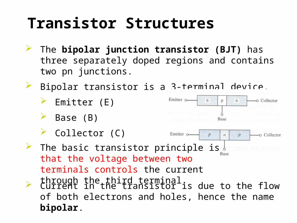
Transistor Structures
The bipolar junction transistor (BJT) has three separately doped regions and contains two pn junctions.
Bipolar transistor is a 3-terminal device.
Emitter (E)
Base (B)
Collector (C)
The basic transistor principle is that the voltage between two terminals controls the current through the third terminal.
Current in the transistor is due to the flow of both electrons and holes, hence the name bipolar.

Transistor Structures There are two types of bipolar junction transistor: npn and
pnp.
The npn bipolar transistor contains a thin p-region between two n-regions.
The pnp bipolar transistor contains a thin n-region sandwiched between two p-regions.

ActiveOperating range of the amplifier.Base-Emitter Junction forward biased.Collector-Base Junction reverse biased
CutoffThe amplifier is basically off. There is voltage but little current.Both junctions reverse biased
SaturationThe amplifier is full on. There is little voltage but lots of current.Both junctions forward biased
3 Regions of Operation

OPERATIONS - npn
The base-emitter (B-E) junction is forward biased and the base-collector (C-B) junction is reverse-biased,.
Since the B-E junction is forward biased, electrons from the emitter are injected across the B-E junction into the base IE
Once in the base region, the electrons are quickly accelerated through the base due to the reverse-biased C-B region IC
ACTIVE MODE
Some electrons, in passing through the base region, recombine with majority carrier holes in the base. This produces the current IB
+
-VBE
iB

C B E
TO ILLUSTRATE
-
VBE
+
•Imagine the marbles as electrons
•A flat base region with gaps where the marbles may fall/trapped – recombine
•A sloping collector region represents high electric field in the C-B region
•Hence, when enough energy is given to the marbles, they will be accelerated towards to base region with enough momentum to pass the base and straight ‘fly’ to the collector

MATHEMATICAL EXPRESSIONS
+
-VBE
IE
IC
IB
IE = IS [ e VBE / VT -1 ] = IS e VBE / VT Based on KCL: IE = IC + IB
No. of electrons crossing the base region and then directly into the collector region is a constant factor of the no. of electrons exiting the base region
IC = IB
No. of electrons reaching the collector region is directly proportional to the no. of electrons injected or crossing the base region.
IC = IEIdeally = 1, but in reality it is between 0.9 and 0.998.

Based on KCL: IE = IC + IB IC = IB IC = IE
IE = IB + IB = IB( + 1)
= [ / + 1 ]
IE = IB( + 1)
NowWith IC = IB IB = IC / Hence, IE = [ IC / ] ( + 1)IC = IE [ / + 1 ]
Comparing with IC = IE
B
C
E
-
+
VEB
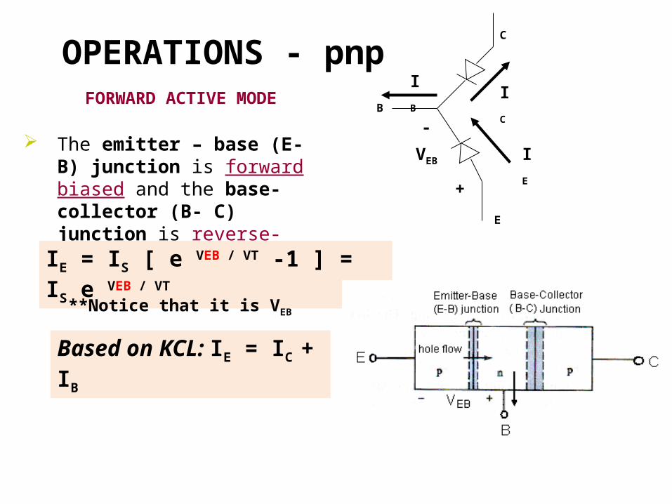
OPERATIONS - pnpFORWARD ACTIVE MODE
The emitter – base (E- B) junction is forward biased and the base-collector (B- C) junction is reverse-biased,.
IE = IS [ e VEB / VT -1 ] = IS e VEB / VT
**Notice that it is VEB
IE
IC
IB
Based on KCL: IE = IC + IB
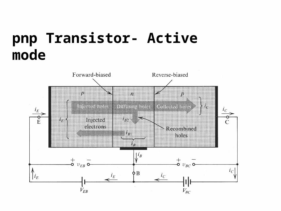
pnp Transistor- Active mode

SUMMARY: Circuit Symbols and Conventions
npn bipolar transistor simple block diagram and circuit symbol.
Arrow is on the emitter terminal that indicates the direction of emitter current (out of emitter terminal for the npn device)
pnp bipolar transistor simple block diagram and circuit symbol.
Arrow is on the emitter terminal that indicates the direction of emitter current (into of emitter terminal for the pnp device)
Based on KCL: IE = IC + IB

IE = IS [ e VBE / VT ]
Based on KCL: IE = IC + IB
IC = IB
IC = IE
= [ / + 1 ]
IE = IB( + 1)
IE = IS [ e VEB / VT]
NPN PNP
= [ / 1 - ]

EXAMPLE 4.1 Calculate the collector and emitter currents, given the base current and current gain. Assume a common-base current gain and a base current of . Also assume that the transistor is biased forward in the forward active mode.
Solution: The common-emitter current gain is
The collector current is
And the emitter current is

Examples
• EXAMPLE 1• Given IB = 6.0A and
IC=510 A
Determine , and IE
• EXAMPLE 2• NPN Transistor • Reverse saturation
current Is = 10-13A with current gain, = 90. Based on VBE = 0.685V, determine IC , IB and IE
EXAMPLE 3 PNP Transistor = 60, IC= 0.85mA Determine , IE and IB

BJT: Current-Voltage CharacteristicIC versus VCE

The Emitter is common to both input (base-emitter) and output (collector-emitter).
Since Emitter is grounded, VC = VCE
With decreasing VC (VCE), the junction B-C will become forward biased too. The current IC quickly drops to zero
because electrons are no longer collected by the collector
Common-Emitter Configuration - npn
Node B
0V

Characteristics of Common-Emitter - npn
NOTE: VEC for PNP