Chapter 3 Device Fabrication TechnologyModern Semiconductor Devices for Integrated Circuits (C. Hu)...
40
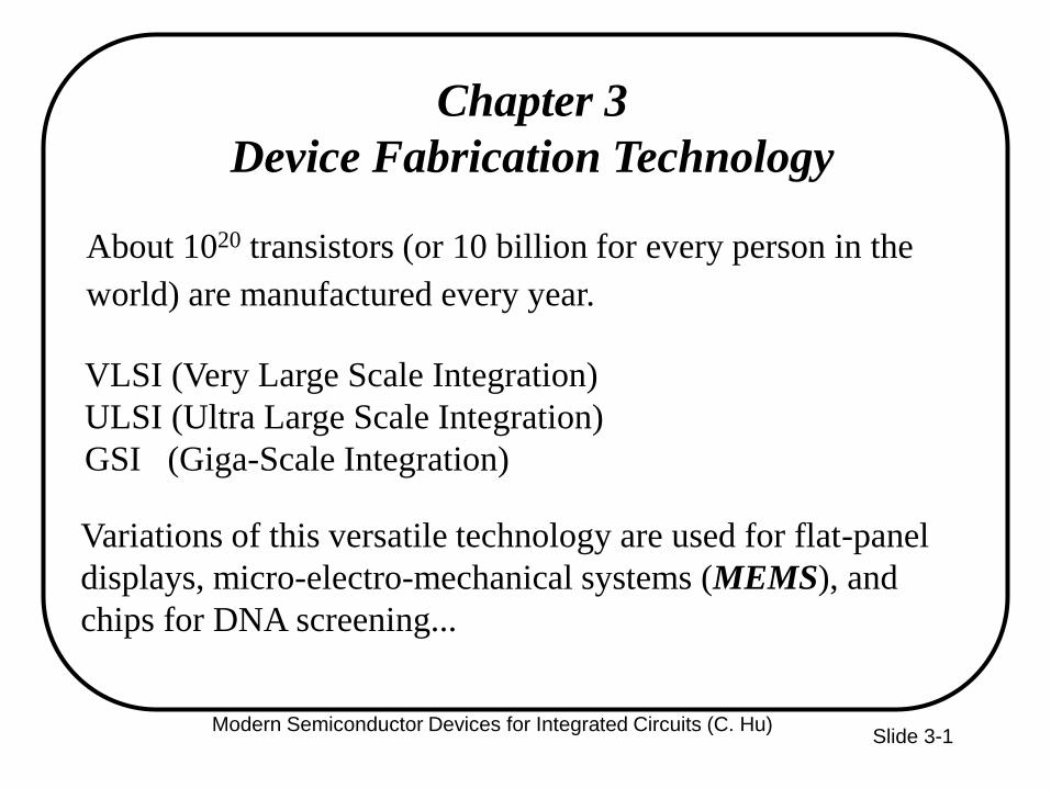
Modern Semiconductor Devices for Integrated Circuits (C. Hu) Slide 3-1 Chapter 3 Device Fabrication Technology About 10 20 transistors (or 10 billion for every person in the world) are manufactured every year. VLSI (Very Large Scale Integration) ULSI (Ultra Large Scale Integration) GSI (Giga-Scale Integration) Variations of this versatile technology are used for flat-panel displays, micro-electro-mechanical systems (MEMS), and chips for DNA screening...
Transcript of Chapter 3 Device Fabrication TechnologyModern Semiconductor Devices for Integrated Circuits (C. Hu)...
Modern Semiconductor Devices for Integrated Circuits (C. Hu)Slide 3-1
Chapter 3
Device Fabrication Technology
About 1020 transistors (or 10 billion for every person in the
world) are manufactured every year.
VLSI (Very Large Scale Integration)
ULSI (Ultra Large Scale Integration)
GSI (Giga-Scale Integration)
Variations of this versatile technology are used for flat-panel
displays, micro-electro-mechanical systems (MEMS), and
chips for DNA screening...
Slide 3-2
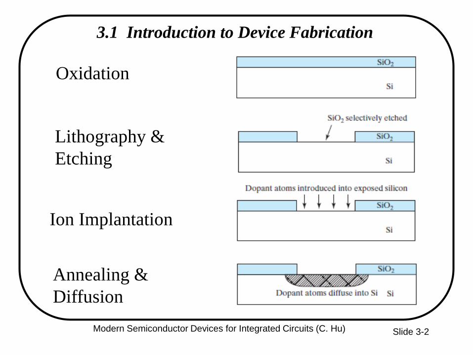
3.1 Introduction to Device Fabrication
Oxidation
Lithography &
Etching
Ion Implantation
Annealing &
Diffusion
Modern Semiconductor Devices for Integrated Circuits (C. Hu)
Slide 3-3
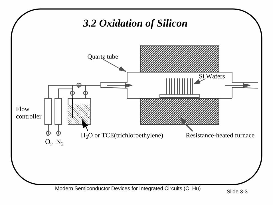
Si Wafers
O2 N2
H2O or TCE(trichloroethylene)
Quartz tube
Resistance-heated furnace
Flowcontroller
3.2 Oxidation of Silicon
Modern Semiconductor Devices for Integrated Circuits (C. Hu)
Slide 3-4
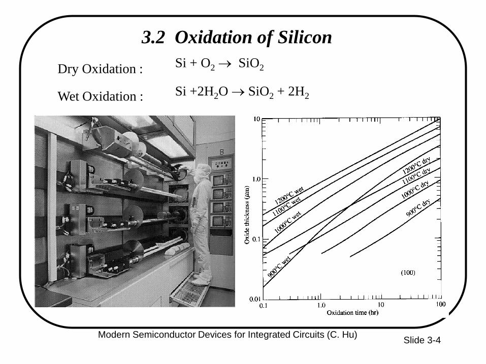
3.2 Oxidation of Silicon
Si + O2 → SiO2
Si +2H2O → SiO2 + 2H2
Dry Oxidation :
Wet Oxidation :
Modern Semiconductor Devices for Integrated Circuits (C. Hu)
Slide 3-5
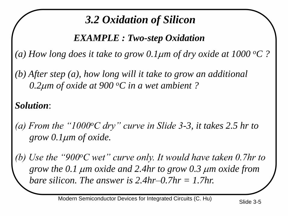
EXAMPLE : Two-step Oxidation
(a) How long does it take to grow 0.1m of dry oxide at 1000 oC ?
(b) After step (a), how long will it take to grow an additional
0.2m of oxide at 900 oC in a wet ambient ?
Solution:
(a) From the “1000oC dry” curve in Slide 3-3, it takes 2.5 hr to
grow 0.1m of oxide.
(b) Use the “900oC wet” curve only. It would have taken 0.7hr to
grow the 0.1 m oxide and 2.4hr to grow 0.3 m oxide from
bare silicon. The answer is 2.4hr–0.7hr = 1.7hr.
3.2 Oxidation of Silicon
Modern Semiconductor Devices for Integrated Circuits (C. Hu)
Slide 3-6
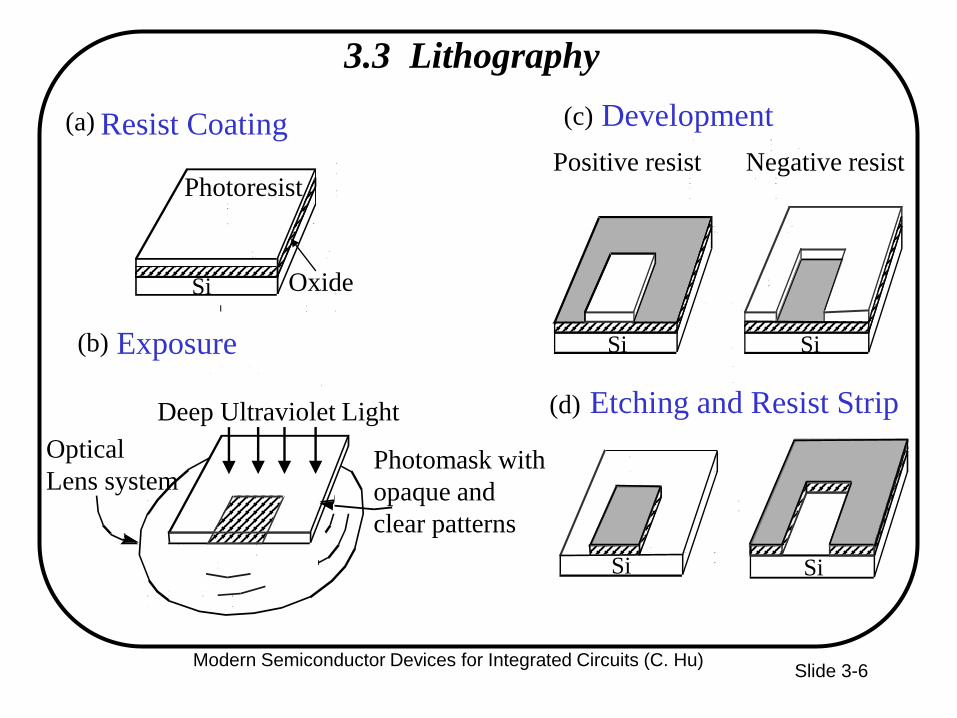
3.3 Lithography
Resist Coating(a) Development(c)
Etching and Resist Strip(d)
Photoresist
OxideSi
Exposure(b) Si Si
Positive resist Negative resist
SiSi
Optical
Lens system
Deep Ultraviolet Light
Photomask with
opaque and
clear patterns
Modern Semiconductor Devices for Integrated Circuits (C. Hu)
Slide 3-7
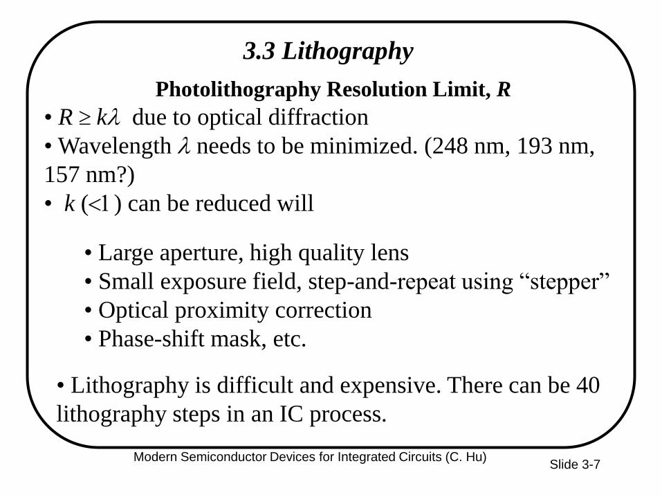
3.3 Lithography
Photolithography Resolution Limit, R
• R kl due to optical diffraction
• Wavelength l needs to be minimized. (248 nm, 193 nm,
157 nm?)
• k (<1) can be reduced will
• Large aperture, high quality lens
• Small exposure field, step-and-repeat using “stepper”
• Optical proximity correction
• Phase-shift mask, etc.
• Lithography is difficult and expensive. There can be 40
lithography steps in an IC process.
Modern Semiconductor Devices for Integrated Circuits (C. Hu)
Slide 3-8
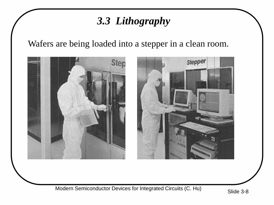
3.3 Lithography
Wafers are being loaded into a stepper in a clean room.
Modern Semiconductor Devices for Integrated Circuits (C. Hu)
Slide 3-9
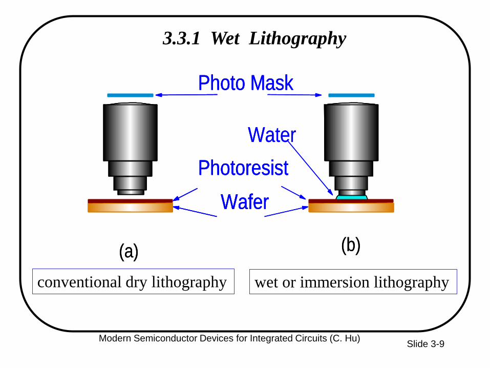
Photo Mask
Photoresist
Wafer
Water
l l
(a) (b)
Photo MaskPhoto Mask
Photoresist
Wafer
Photoresist
Wafer
Water
ll ll
(a) (b)
conventional dry lithography wet or immersion lithography
3.3.1 Wet Lithography
Modern Semiconductor Devices for Integrated Circuits (C. Hu)
Slide 3-10
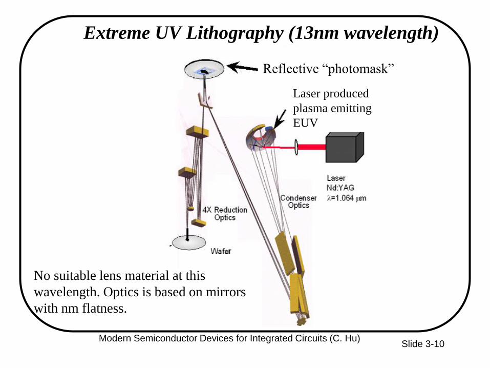
Reflective “photomask”
Laser produced
plasma emitting
EUV
Extreme UV Lithography (13nm wavelength)
No suitable lens material at this
wavelength. Optics is based on mirrors
with nm flatness.
Modern Semiconductor Devices for Integrated Circuits (C. Hu)
Slide 3-11
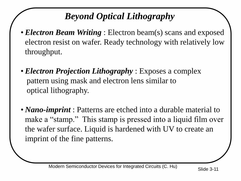
• Electron Beam Writing : Electron beam(s) scans and exposed
electron resist on wafer. Ready technology with relatively low
throughput.
• Electron Projection Lithography : Exposes a complex
pattern using mask and electron lens similar to
optical lithography.
• Nano-imprint : Patterns are etched into a durable material to
make a “stamp.” This stamp is pressed into a liquid film over
the wafer surface. Liquid is hardened with UV to create an
imprint of the fine patterns.
Beyond Optical Lithography
Modern Semiconductor Devices for Integrated Circuits (C. Hu)
Slide 3-12
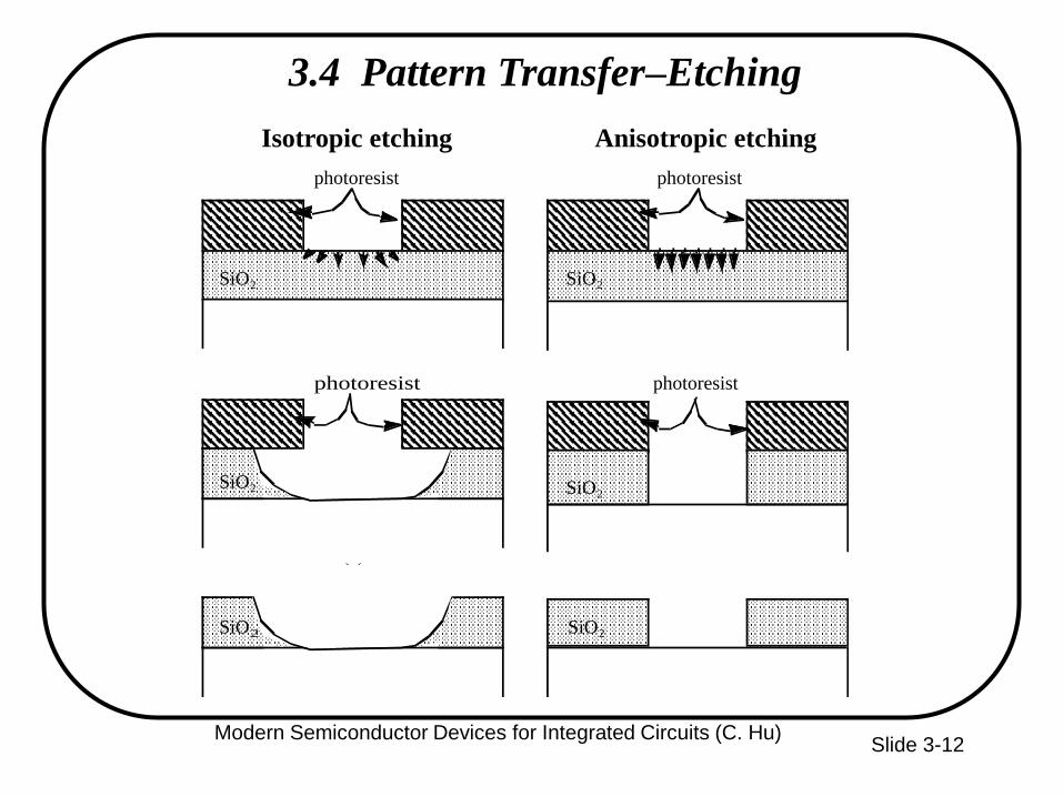
3.4 Pattern Transfer–Etching
Isotropic etching Anisotropic etching
SiO2
SiO2
SiO2
(1)
(2)
(3)
photoresist
photoresist
SiO2
(1)
(2)
photoresist
photoresist
SiO2
SiO2
(3)
(a) Isotropic wet etching (b) Anisotropic dry etching.Modern Semiconductor Devices for Integrated Circuits (C. Hu)
Slide 3-13
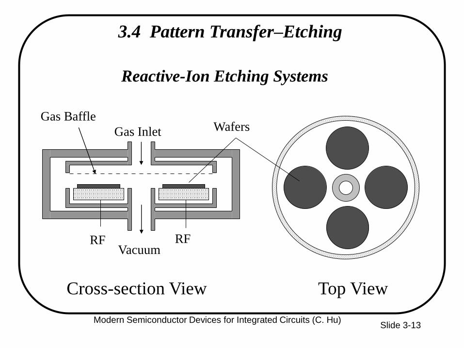
3.4 Pattern Transfer–Etching
Cross-section View Top View
Reactive-Ion Etching Systems
Gas Inlet
RFVacuum
WafersGas Baffle
RF
Modern Semiconductor Devices for Integrated Circuits (C. Hu)
Slide 3-14
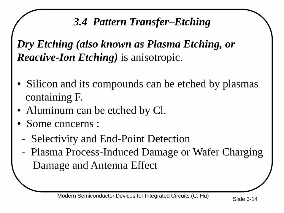
3.4 Pattern Transfer–Etching
Dry Etching (also known as Plasma Etching, or
Reactive-Ion Etching) is anisotropic.
• Silicon and its compounds can be etched by plasmas
containing F.
• Aluminum can be etched by Cl.
• Some concerns :
- Selectivity and End-Point Detection
- Plasma Process-Induced Damage or Wafer Charging
Damage and Antenna Effect
Modern Semiconductor Devices for Integrated Circuits (C. Hu)
Slide 3-15
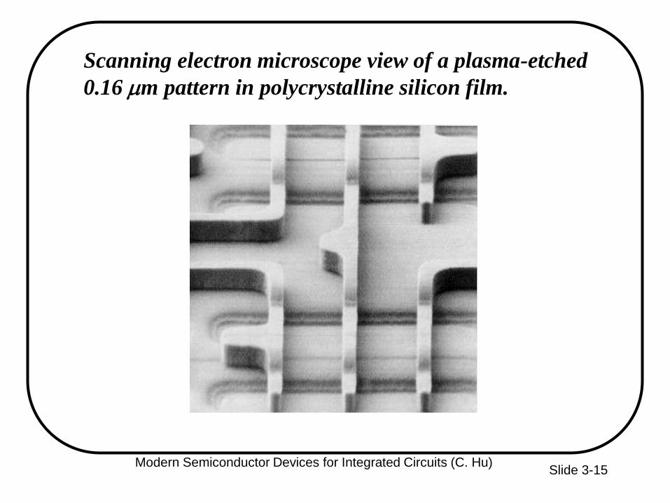
Scanning electron microscope view of a plasma-etched
0.16 m pattern in polycrystalline silicon film.
Modern Semiconductor Devices for Integrated Circuits (C. Hu)
Slide 3-16
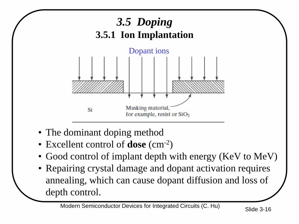
3.5 Doping3.5.1 Ion Implantation
• The dominant doping method
• Excellent control of dose (cm-2)
• Good control of implant depth with energy (KeV to MeV)
• Repairing crystal damage and dopant activation requires
annealing, which can cause dopant diffusion and loss of
depth control.
Dopant ions
Modern Semiconductor Devices for Integrated Circuits (C. Hu)
Slide 3-17
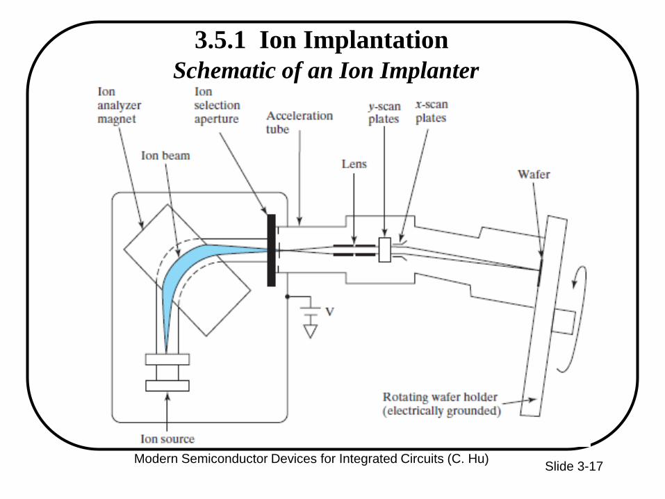
3.5.1 Ion Implantation
Schematic of an Ion Implanter
Modern Semiconductor Devices for Integrated Circuits (C. Hu)
Slide 3-18
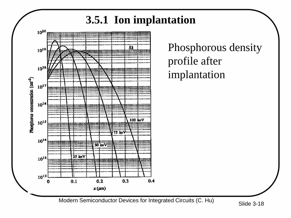
3.5.1 Ion implantation
Phosphorous density
profile after
implantation
Modern Semiconductor Devices for Integrated Circuits (C. Hu)

Slide 3-19
3.5.1 Ion Implantation
Model of Implantation Doping Profile (Gaussian)
22 2/)(
)(2)( RRxi e
R
NxN −−
=
Ni : dose (cm-2)
R : range or depth
R : spread or sigma
Modern Semiconductor Devices for Integrated Circuits (C. Hu)
Slide 3-20
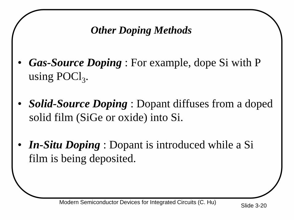
Other Doping Methods
• Gas-Source Doping : For example, dope Si with P
using POCl3.
• Solid-Source Doping : Dopant diffuses from a doped
solid film (SiGe or oxide) into Si.
• In-Situ Doping : Dopant is introduced while a Si
film is being deposited.
Modern Semiconductor Devices for Integrated Circuits (C. Hu)
Slide 3-21
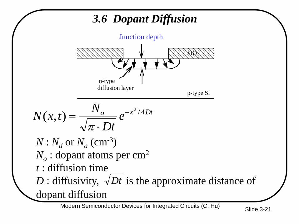
3.6 Dopant Diffusion
Dtxo eDt
NtxN 4/2
),( −
=
N : Nd or Na (cm-3)
No : dopant atoms per cm2
t : diffusion time
D : diffusivity, is the approximate distance of
dopant diffusion
Dt
p-type Si
SiO2
n-type diffusion layer
Junction depth
Modern Semiconductor Devices for Integrated Circuits (C. Hu)
Slide 3-22
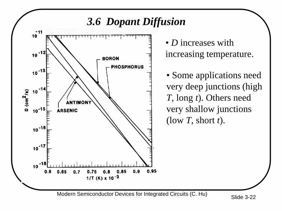
3.6 Dopant Diffusion
• Some applications need
very deep junctions (high
T, long t). Others need
very shallow junctions
(low T, short t).
• D increases with
increasing temperature.
Modern Semiconductor Devices for Integrated Circuits (C. Hu)
Slide 3-23
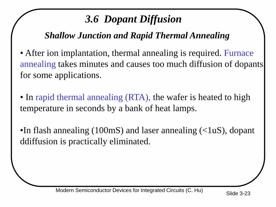
3.6 Dopant Diffusion
Shallow Junction and Rapid Thermal Annealing
• After ion implantation, thermal annealing is required. Furnace
annealing takes minutes and causes too much diffusion of dopants
for some applications.
• In rapid thermal annealing (RTA), the wafer is heated to high
temperature in seconds by a bank of heat lamps.
•In flash annealing (100mS) and laser annealing (<1uS), dopant
ddiffusion is practically eliminated.
Modern Semiconductor Devices for Integrated Circuits (C. Hu)
Slide 3-24
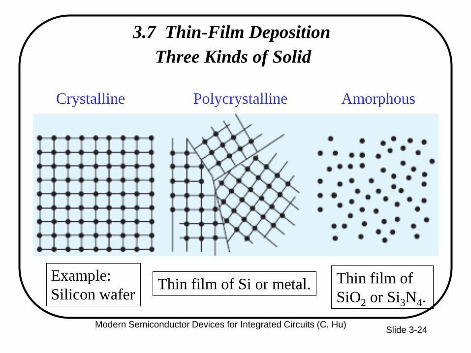
3.7 Thin-Film Deposition
Three Kinds of Solid
Crystalline Polycrystalline
Example:
Silicon waferThin film of Si or metal. Thin film of
SiO2 or Si3N4.
Amorphous
Modern Semiconductor Devices for Integrated Circuits (C. Hu)
Slide 3-25
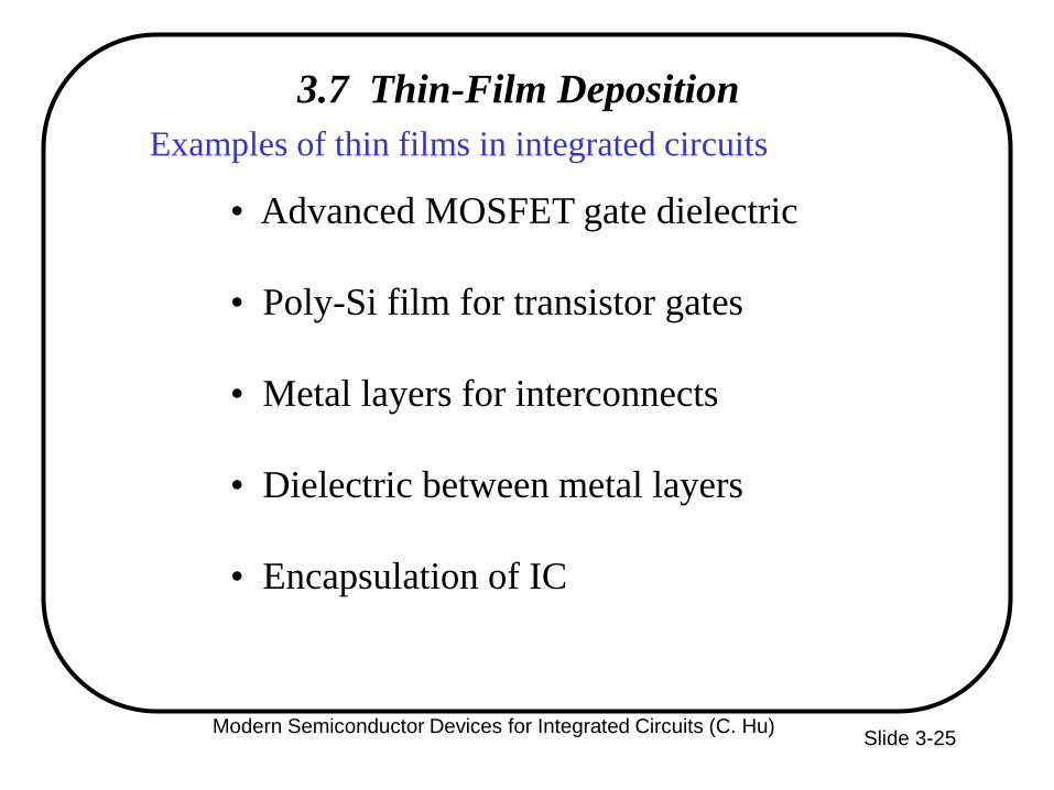
3.7 Thin-Film Deposition
• Advanced MOSFET gate dielectric
• Poly-Si film for transistor gates
• Metal layers for interconnects
• Dielectric between metal layers
• Encapsulation of IC
Examples of thin films in integrated circuits
Modern Semiconductor Devices for Integrated Circuits (C. Hu)
Slide 3-26
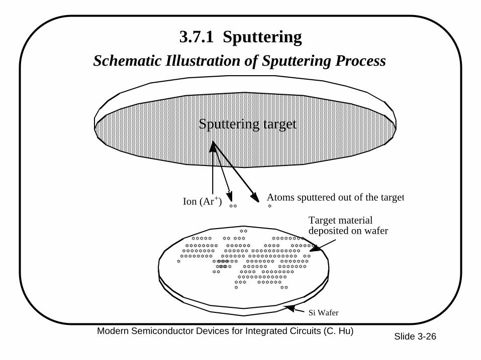
3.7.1 Sputtering
YYYYYYYY
YYYYYYYY
YYYYYYYY
YYYYYY
YYYYYY
Y YYYY
YYYYYY
YYYYY
YYYY YYYYYY
YYYYYYYYYYYY
YYYYYYYYYYYY YY
YYYYYYY YYYYYYY
YYYYYY YYYYYYY
YYYY YYYYYYYY
YYYYYYYYYYYY
YYY YYYYYY
YYYYYY
YY
Y YY
YYY YYYYYYYYYYYYY YY
YY
Target materialdeposited on wafer
Si Wafer
Ion (Ar+)YY Y
Sputtering target
Atoms sputtered out of the target
Schematic Illustration of Sputtering Process
Modern Semiconductor Devices for Integrated Circuits (C. Hu)
Slide 3-27
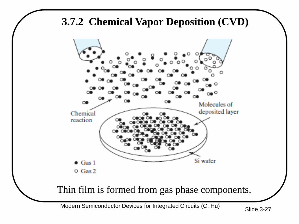
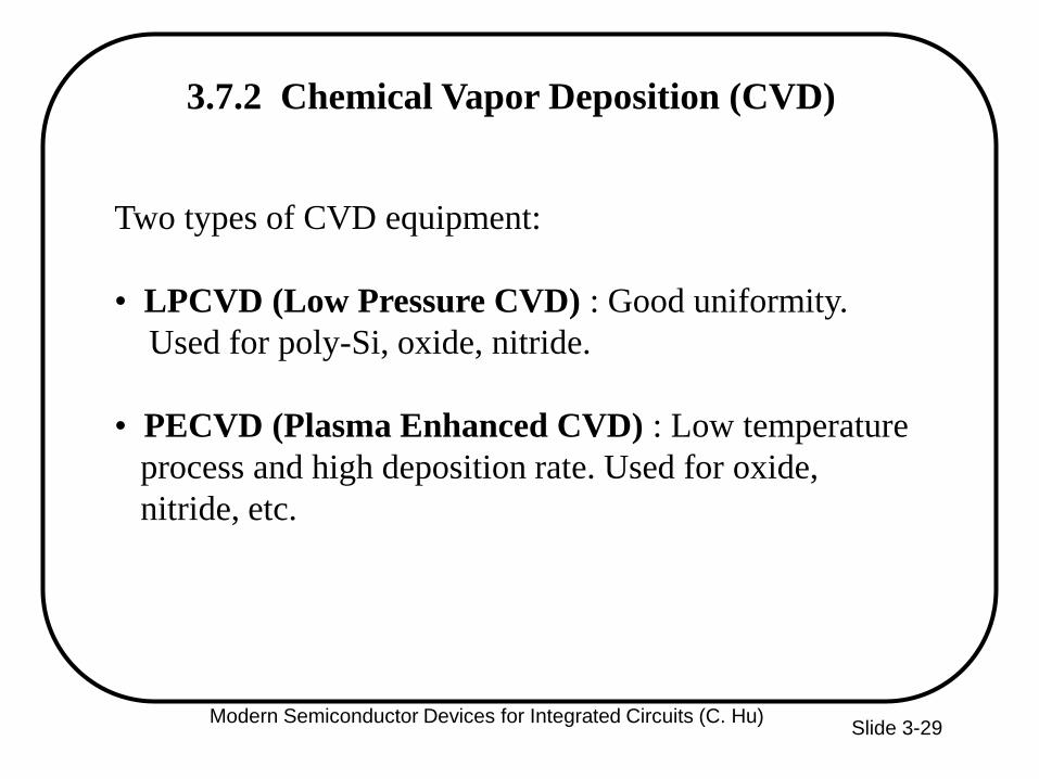
3.7.2 Chemical Vapor Deposition (CVD)
Thin film is formed from gas phase components.
Modern Semiconductor Devices for Integrated Circuits (C. Hu)
Slide 3-28
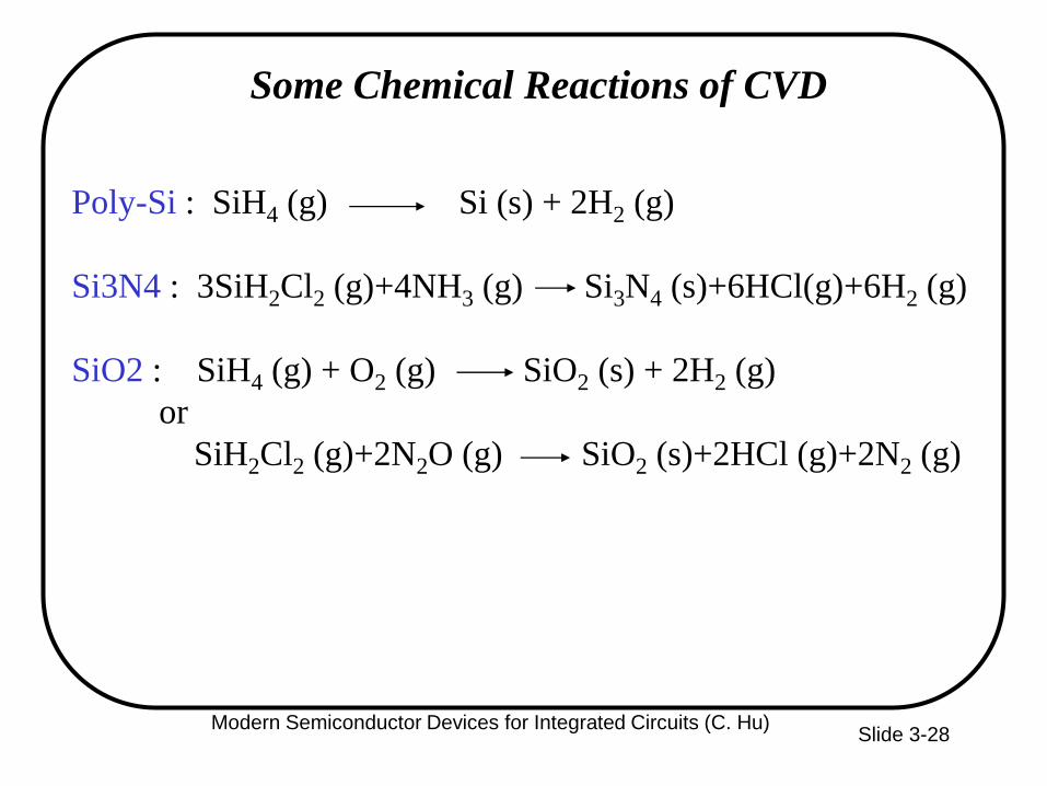
Some Chemical Reactions of CVD
Poly-Si : SiH4 (g) Si (s) + 2H2 (g)
Si3N4 : 3SiH2Cl2 (g)+4NH3 (g) Si3N4 (s)+6HCl(g)+6H2 (g)
SiO2 : SiH4 (g) + O2 (g) SiO2 (s) + 2H2 (g)
or
SiH2Cl2 (g)+2N2O (g) SiO2 (s)+2HCl (g)+2N2 (g)
Modern Semiconductor Devices for Integrated Circuits (C. Hu)
Slide 3-29
Two types of CVD equipment:
• LPCVD (Low Pressure CVD) : Good uniformity.
Used for poly-Si, oxide, nitride.
• PECVD (Plasma Enhanced CVD) : Low temperature
process and high deposition rate. Used for oxide,
nitride, etc.
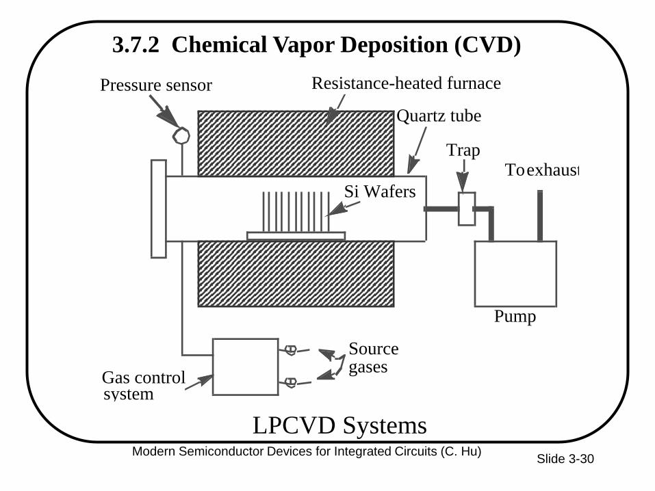
3.7.2 Chemical Vapor Deposition (CVD)
Modern Semiconductor Devices for Integrated Circuits (C. Hu)
Slide 3-30
Si Wafers
Quartz tube
Resistance-heated furnacePressure sensor
Gas control
Source gases
Pump
Trap exhaust To
system
LPCVD Systems
3.7.2 Chemical Vapor Deposition (CVD)
Modern Semiconductor Devices for Integrated Circuits (C. Hu)
Slide 3-31
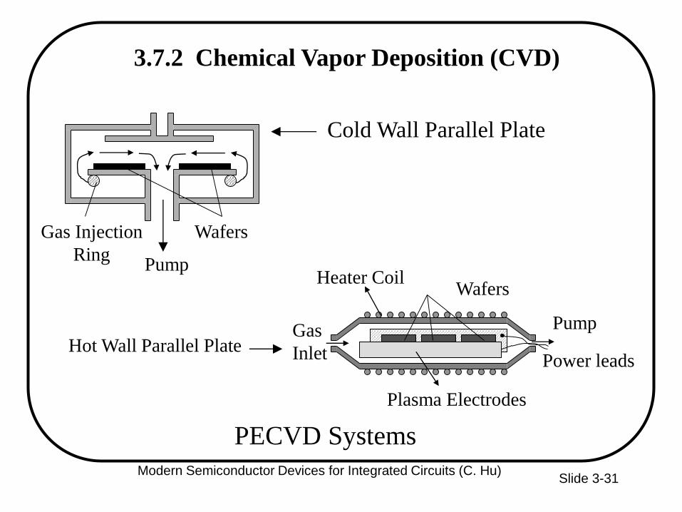
3.7.2 Chemical Vapor Deposition (CVD)
PECVD Systems
Cold Wall Parallel Plate
Hot Wall Parallel Plate
Pump
Plasma Electrodes
Power leads
Wafers
Gas
Inlet
WafersGas Injection
RingPump
Heater Coil
Modern Semiconductor Devices for Integrated Circuits (C. Hu)
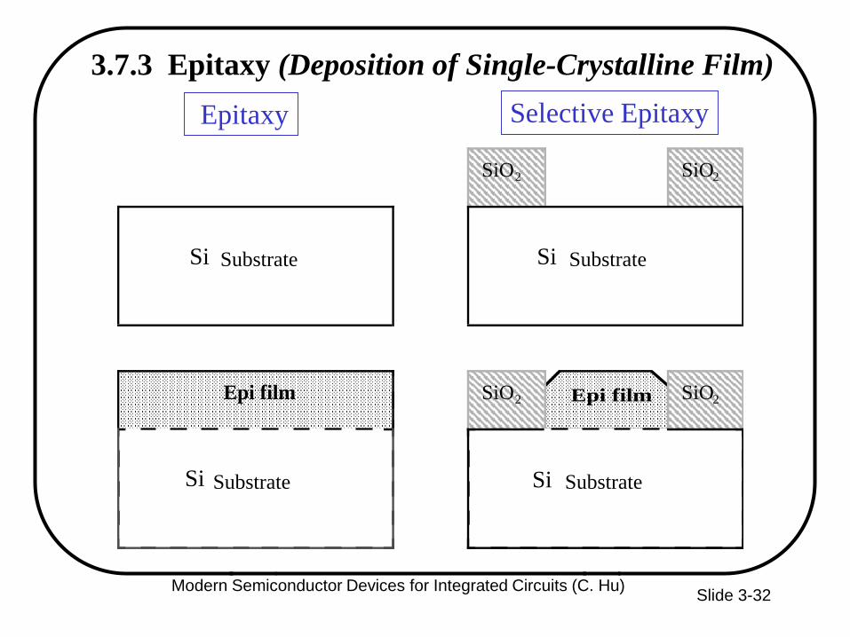
SiO2 SiO2
Substrate
SiO2 SiO2
Substrate
Epi film
(b)
Substrate
Substrate
Epi film
(a)
Si Si
Si Si
Slide 3-32
3.7.3 Epitaxy (Deposition of Single-Crystalline Film)
Epitaxy Selective Epitaxy
Modern Semiconductor Devices for Integrated Circuits (C. Hu)
Slide 3-33
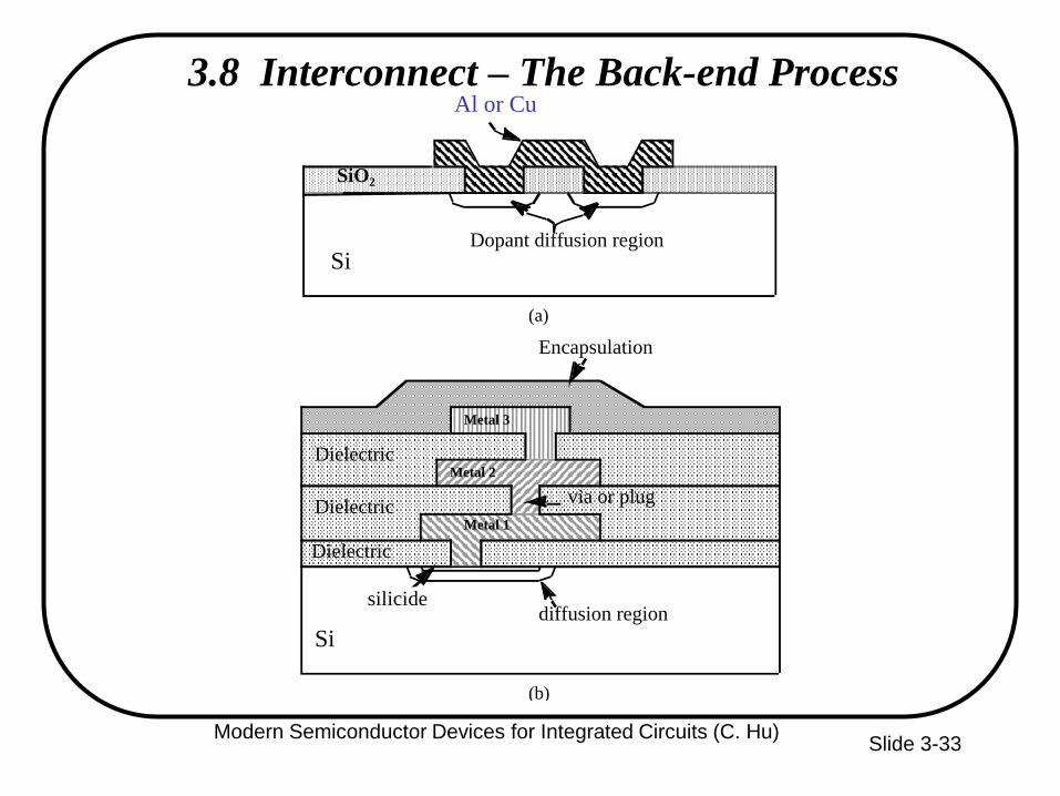
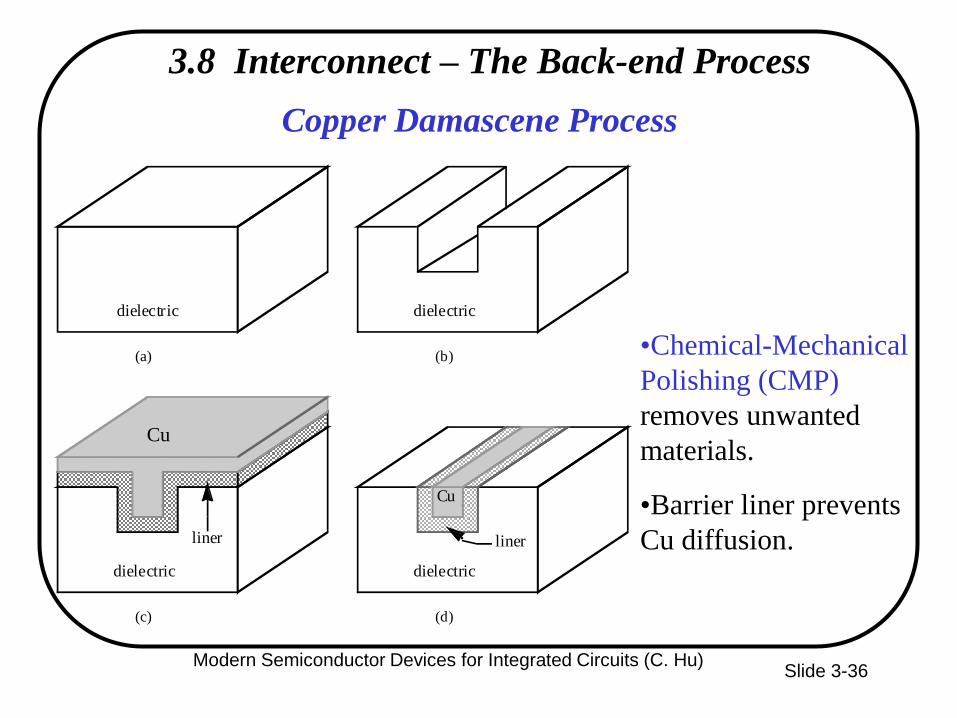
3.8 Interconnect – The Back-end Process
Dopant diffusion regionSi
SiO2
Al-Cu
(a)
Sidiffusion region
CoSi2
Metal 1
Metal 2
Metal 3
Dielectric
Dielectric
Encapsulation
(b)
Dielectric
via or plug
silicide
Al or Cu
Modern Semiconductor Devices for Integrated Circuits (C. Hu)
Slide 3-34
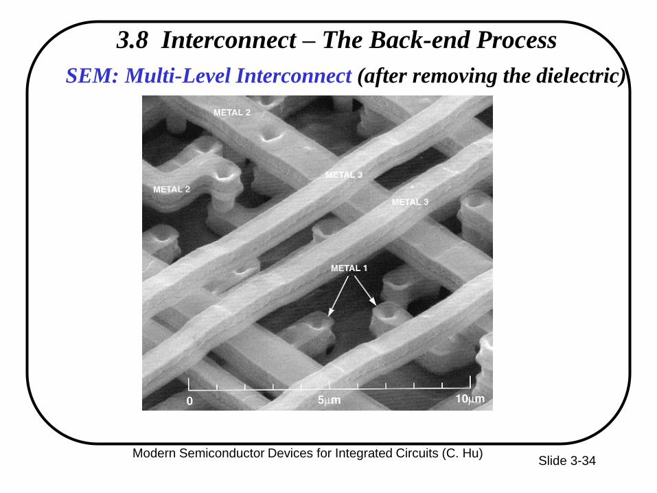
SEM: Multi-Level Interconnect (after removing the dielectric)
3.8 Interconnect – The Back-end Process
Modern Semiconductor Devices for Integrated Circuits (C. Hu)
Slide 3-35
Copper Interconnect
• Al interconnect is prone to voids formation by
electromigration.
• Cu has excellent electromigration reliability
and 40% lower resistance than Al.
• Because dry etching of copper is difficult (copper
etching products tend to be non-volatile), copper
patterns are defined by a damascene process.
3.8 Interconnect – The Back-end Process
Modern Semiconductor Devices for Integrated Circuits (C. Hu)
Slide 3-36
dielectric
dielectric dielectric
dielectric
Cu
Cu
liner liner
(a) (b)
(c) (d)
Copper Damascene Process
•Chemical-Mechanical
Polishing (CMP)
removes unwanted
materials.
•Barrier liner prevents
Cu diffusion.
3.8 Interconnect – The Back-end Process
Modern Semiconductor Devices for Integrated Circuits (C. Hu)
Slide 3-37
3.8 Interconnect – The Back-end Process
Planarization
• A flat surface is highly desirable for subsequent
lithography and etching.
• CMP (Chemical-Mechanical Polishing) is used
to planarize each layer of dielectric in the
interconnect system. Also used in the front-end
process.
Modern Semiconductor Devices for Integrated Circuits (C. Hu)
Slide 3-38
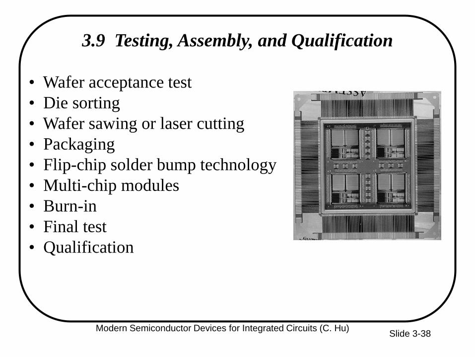
3.9 Testing, Assembly, and Qualification
• Wafer acceptance test
• Die sorting
• Wafer sawing or laser cutting
• Packaging
• Flip-chip solder bump technology
• Multi-chip modules
• Burn-in
• Final test
• Qualification
Modern Semiconductor Devices for Integrated Circuits (C. Hu)
Slide 3-39
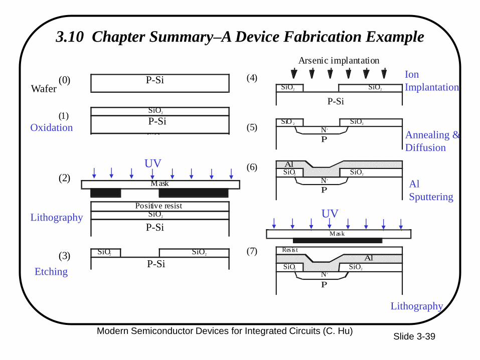
3.10 Chapter Summary–A Device Fabrication Example
Wafer
Oxidation
Lithography
Etching
Annealing &
Diffusion
Al
Sputtering
(0)
Positive resist SiO2
P-Si
P-Si
SiO2
P-Si
Mask
UV
SiO2 SiO2
SiO2 SiO2
SiO 2 SiO2
P-Si
PN+
SiO2 SiO2
PN+
P-Si
SiO2 SiO2
P
N+
Mask
Al Res is t
SiO2 SiO2
PN+
(1)
(2)
(4)
Arsenic implantation
Al
UV
(7)
(3)
(5)
(6)
(8)
(9)
SiO2 SiO2
PN+
SiO2 SiO2
PN+
(10)
SiO2
SiO2
PN+
(11)
SiO2 SiO 2
PN+
(12)
SiO2 SiO2
PN
+
(13)
Al
Si3 N4
Si3N
4
Si3 N4
Si3 N4
Si3N
4
Al
Al
Al
Al
Al
Photoresist
Au
Au
wire
Plastic package
metal leads
SiO2
Al
UV
Lithography
(0)
Positive resist SiO2
P-Si
P-Si
SiO2
P-Si
Mask
UV
SiO2 SiO2
SiO2 SiO2
SiO 2 SiO2
P-Si
PN+
SiO2 SiO2
PN+
P-Si
SiO2 SiO2
P
N+
Mask
Al Res is t
SiO2 SiO2
PN+
(1)
(2)
(4)
Arsenic implantation
Al
UV
(7)
(3)
(5)
(6)
(8)
(9)
SiO2 SiO2
PN+
SiO2 SiO2
PN+
(10)
SiO2
SiO2
PN+
(11)
SiO2 SiO 2
PN+
(12)
SiO2 SiO2
PN
+
(13)
Al
Si3 N4
Si3N
4
Si3 N4
Si3 N4
Si3N
4
Al
Al
Al
Al
Al
Photoresist
Au
Au
wire
Plastic package
metal leads
SiO2
Al
UV
Ion
Implantation
Modern Semiconductor Devices for Integrated Circuits (C. Hu)
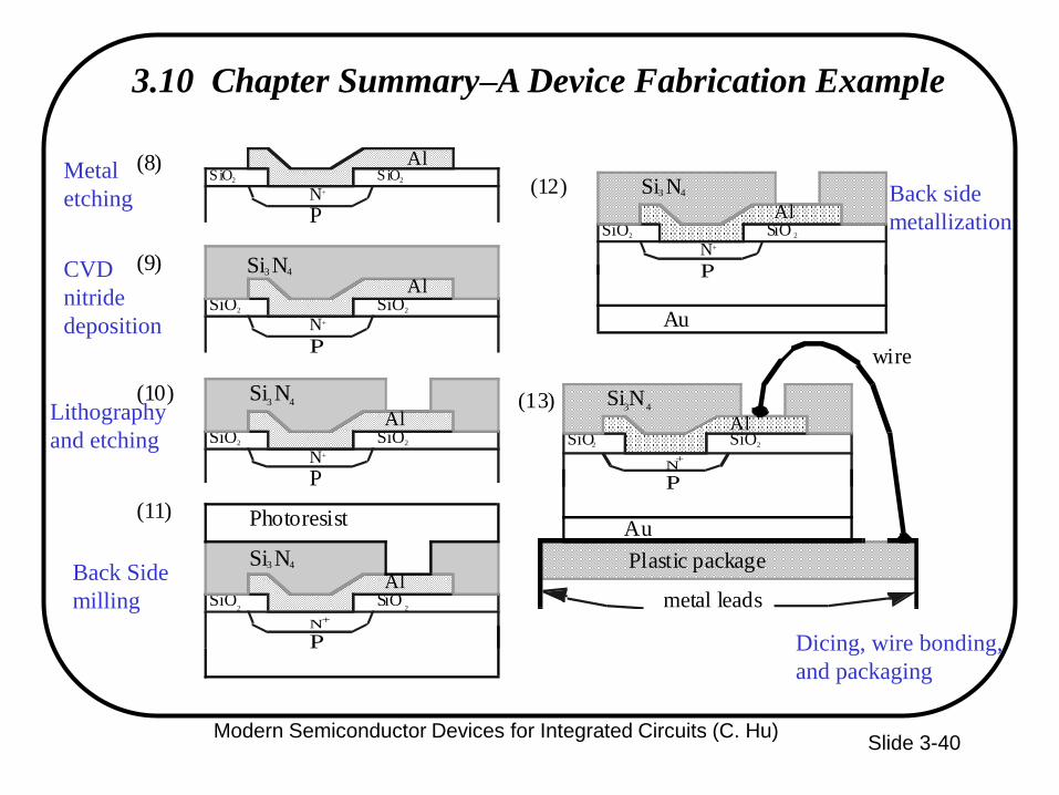
Slide 3-40
Metal
etching
CVD
nitride
deposition
Lithography
and etching
Back Side
milling
Back side
metallization
Dicing, wire bonding,
and packaging
3.10 Chapter Summary–A Device Fabrication Example
(0)
Positive resist SiO2
P-Si
P-Si
SiO2
P-Si
Mask
UV
SiO2 SiO2
SiO2 SiO2
SiO 2 SiO2
P-Si
PN+
SiO2 SiO2
PN+
P-Si
SiO2 SiO2
P
N+
Mask
Al Res is t
SiO2 SiO2
PN+
(1)
(2)
(4)
Arsenic implantation
Al
UV
(7)
(3)
(5)
(6)
(8)
(9)
SiO2 SiO2
PN+
SiO2 SiO2
PN+
(10)
SiO2
SiO2
PN+
(11)
SiO2 SiO 2
PN+
(12)
SiO2 SiO2
PN
+
(13)
Al
Si3 N4
Si3N
4
Si3 N4
Si3 N4
Si3N
4
Al
Al
Al
Al
Al
Photoresist
Au
Au
wire
Plastic package
metal leads
SiO2
Al
Modern Semiconductor Devices for Integrated Circuits (C. Hu)