Chapter 3 – Computer Hardware Computer Components – Hardware (cont.) Lecture 3.

23©2015 Gilbert Ndjatou
Chapter 2
COMPUTER SYSTEM
HARDWARE
A digital computer system consists of hardware and software. Thehardware consists of the physical components of the system, whereas the
software is the collection of programs that the computer can execute. Thischapter discusses the major components of a digital computer system’shardware, with an emphasis on Intel 8086 processor based computer systems.The software environment of a digital computer system is discussed inchapter 5.
Figure 2.1 shows a schematic representation of the four majorcomponents of a digital computer system’s hardware, and how they areinterconnected. These major components are the Central Processing Unit(CPU), the Main (or Primary) Memory, the input system, and the outputsystem.
The input system consists of the input devices with their controllers,
whereas the output system consists of the output devices with their
controllers. Computer components other than the processor and the main
memory are referred to as the system peripherals.

24
©2015 Gilbert Ndjatou
Figure 2.1 General Structure of a Digital Computer System
The arrows indicate the flow of data between the computer components.
Exercise 2.1
Fill in the blanks with the most appropriate answers.
1. A digital computer system consists of ____________________ and ______________________.
2. The ______________________________ consists of the physical components of the system.
3. The _________________________ is the collection of programs that the computer can execute.
4. The four major components of a digital computer system hardware are: _____________
_____________________________________________________________________________
5. Computer components other than the processor and the main memory are referred to as the
system _______________________________________________________________________.

25
©2015 Gilbert Ndjatou
2.1 Main Memory
The Main Memory (also known as primary memory) is a collection of two-
state devices that are used to represent binary digits 0 and 1: when the device
is in one state it is said to represent bit 1, and when it is in the other state, it
is said to represent bit 0. It holds the data to be processed by the computer,
and the program that is executed in order to process it.
Consecutive bits in the main memory are grouped into units of 8 called
bytes. Each byte is identified by its relative position in the main memory,
referred to as physical address or absolute address.
In an Intel 8086 processor based computer system, an absolute address
is a 20-bit (5 hexadecimal digits) integer. That is, the first byte is at physical
address 00000h, the second at physical address 00001h, and the last byte is
at physical address FFFFFh. It then follows that the main memory of an Intel
8086 processor based computer can have a maximum of 2 (or 1,048,576)20
bytes.
The capacity of the main memory is the number of bytes that it
contains. It is measured in kilobytes (KB), with one kilobyte equals 2 (or10
1024) bytes. Larger units are megabyte and gigabyte. One megabyte (MB)
equals 2 (or 1,048,576) bytes, and one gigabyte (GB) equals 2 (or20 30
1,078,741,824) bytes.
The contents of a byte is the 8-bit pattern that it represents. It may be
specified either in binary or in hexadecimal. For example, if the byte in the
main memory at physical address 05A84h is represented by the sequence of
bits 1 0 1 1 0 0 1 1b which corresponds to the hexadecimal number B3h,
then its contents is either 10110011b or B3h.
Memory Units
In order to conveniently store data in the main memory, consecutive bytes are
grouped into units of 2, 4, 8, or 10. The following memory units are used in
Intel 8086 processor based computers:
a word is a group of 2 consecutive bytes (16 bits),
a doubleword a group of 4 consecutive bytes (2 words or 32 bits),

26
©2015 Gilbert Ndjatou
a quadword a group of 8 consecutive bytes (4 words or 64 bits), and
a tenbyte a group of 10 consecutive bytes (5 words or 80 bits).
The address of a memory unit (word, doubleword, quadword, or tenbyte)
is the address of the first byte in the unit.
Memory Organization
The memory of an Intel 8086 processor based computer is organized into
paragraphs, pages, and segments. In Figure 2.2, the main memory is
represented as a collection of paragraphs.
A paragraph is a group of 16 consecutive bytes (or 8 words) that starts
at a physical address divisible by 16. A physical address of this type is said
to be a paragraph boundary. Note that an hexadecimal integer is divisible
by 16 if its right-most digit is 0. As you can see in Figure 2.2, the first
paragraph starts at physical address 00000h, the second at physical address
00010h, . . . , and the last one at physical address FFFF0h.
Each paragraph is identified with a 4-digit hexadecimal integer which
corresponds to its relative position in the main memory: The first paragraph
is identified with 0000h, the second with 0001h, . . . , and the last one with
FFFFh. You may notice in Figure 2.2 that 4-digit hexadecimal integer that
identifies a paragraph is the physical address of the first byte in that paragraph
divided by 16. That means, with the right-most digit deleted. For example,
the physical address of the first byte in the paragraph identified with 01A6h
is 01A60h. Also, if the physical address of the first byte of a paragraph is
25D50h, then that paragraph is identified with 25D5h.
A page is a group of 16 consecutive paragraphs (or 256 consecutive
bytes starting at a paragraph boundary), and a segment (also called frame)
is a group of one or more consecutive paragraphs with up to 64 KB (256
pages). Segments are identified with the relative position of their first
paragraph: a segment selector is the 4-digit hexadecimal integer that
identifies its first paragraph.

27
©2015 Gilbert Ndjatou
Segments play a major role in the addressing of bytes in the main
memory: in each segment, a byte is uniquely identified with its relative
position in that segment, specified as a 4-digit hexadecimal integer called
offset. The first byte in each segment is at offset 0000h, the second at offset
0001h, . . . , and the last byte (in a segment of 64 KB) is at offset FFFFh.
Notice in Figure 2.2 that segments may overlap: a byte may belong to
more than one segment. For example, the byte at physical address 0005Bh
belongs respectively to the segments with segment selectors 0000h, 0001h,
0002h, 0003h, 0004h, and 0005h. The canonic frame of a byte is the frame
with the largest segment selector in which it belongs.
Figure 2.2 Memory Organization
Segment
Selector
Physical address
of first byte
Paragraphs
0000 00000
0001 00010
0002 00020
.
.
.
FFFE FFFE0
FFFF FFFF0
The offset of a byte in its canonic frame is a number from 0000h to
000Fh. By dividing the physical address of a byte by 16, the quotient is the
selector of its canonic frame, and the remainder is the offset of that byte in
the canonic frame. For example, the canonic frame of the byte at physical
address 0005Bh has selector 0005h, and its offset in the canonic frame is
000Bh. Similarly, the canonic frame of the byte at physical address 5AC23h
has the selector 5AC2h, and its offset in its canonic frame is 0003h.
28
©2015 Gilbert Ndjatou
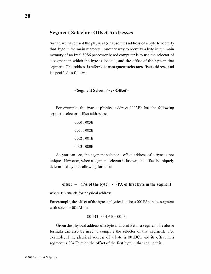
Segment Selector: Offset Addresses
So far, we have used the physical (or absolute) address of a byte to identify
that byte in the main memory. Another way to identify a byte in the main
memory of an Intel 8086 processor based computer is to use the selector of
a segment in which the byte is located, and the offset of the byte in that
segment. This address is referred to as segment selector:offset address, and
is specified as follows:
<Segment Selector> : <Offset>
For example, the byte at physical address 0003Bh has the following
segment selector: offset addresses:
0000 : 003B
0001 : 002B
0002 : 001B
0003 : 000B
As you can see, the segment selector : offset address of a byte is not
unique. However, when a segment selector is known, the offset is uniquely
determined by the following formula:
offset = (PA of the byte) - (PA of first byte in the segment)
where PA stands for physical address.
For example, the offset of the byte at physical address 001B3h in the segment
with selector 001Ah is:
001B3 - 001A0 = 0013.
Given the physical address of a byte and its offset in a segment, the above
formula can also be used to compute the selector of that segment. For
example, if the physical address of a byte is 001BCh and its offset in a
segment is 004Ch, then the offset of the first byte in that segment is:

29
©2015 Gilbert Ndjatou
001BC - 004C = 00170.
Therefore, the selector of that segment is 0017.
Given the selector : offset address of a byte, its physical address is
computed by the formula:
PA = (PA of first byte in the segment) + offset
For example, the physical address of the byte with segment selector : offset
address 1B2C : 001A is: 1B2C0 + 001A = 1B2DA.
Example 2.1 illustrates the use of the above formulas.
Example 2.1 Segment Selector: Offset Address - Physical Address
1) The physical address of the byte with segment selector : offset address 2AB5:037F is:
2AB50 + 037F = 2AECF.
2) If the physical address of a byte is 16B2A,
i) what is its offset in the segment with selector 15A1?
ii) what is the segment selector of the segment in which its offset is 011A?
iii) what is its segment selector : offset address in the canonic frame?
Answers:
i) its offset is: 16B2A - 15A10 = 111A
ii) the PA of the first byte in that segment is: 16B2A - 011A = 16A10; the segment selector
is therefore: 16A1.
iii) the segment selector : offset address in the canonic frame is: 16B2: 000A.

30
©2015 Gilbert Ndjatou
RAM and ROM
Two types of memory are used in most computer systems today: the random
access memory (RAM) and the read only memory (ROM).
The RAM is used to temporarily hold programs to be executed on the
computer and their data. Information can be stored, and also retrieved from
the RAM. However, the RAM is volatile: its contents are lost when the
power to the computer is turned off.
The ROM is a non-volatile memory. Unlike the RAM, information can
only be retrieved from it: its contents cannot be changed by the programmer.
It is used by computer manufacturer to store programs and data that must be
available immediately after the computer is turned on to control the
operations of the CPU.
Exercise 2.2
Part I Fill in the blanks with the most appropriate answers.
1. The ________________________________ is a collection of two-state devices that are used
to represent binary digits, 0 and 1.
2. The _________________________________ holds the data to be processed by the computer,
and the program that is executed in order to process it.
3. Consecutive bits in the main memory are grouped into units of 8 called ____________________.
4. The ______________________________ of a byte in the memory corresponds to its relative
position in the main memory.
5. The _______________________ of the main memory is the number of bytes that it contains.
6. The capacity of the main memory is measured in _____________________________________.
7. A kilobyte (KB) is: ____________________________________________ bytes.
8. A megabyte (MB) is: ___________________________________________ bytes.
9. A gigabyte (GB) is : ____________________________________________ bytes.
10. The ___________________________________ of a byte is the 8-bit pattern that it represents.

31
©2015 Gilbert Ndjatou
The following questions are related to Intel 8086 processor based computers.
11. A _____________________________ is a group of 2 consecutive bytes (16 bits).
12. A _____________________________ is a group of 4 consecutive bytes (2 words or 32 bits).
13. A _____________________________ is a group of 8 consecutive bytes (4 words or 64 bits).
14. A _____________________________ is a group of 10 consecutive bytes (5 words or 80 bits).
15. A _____________________________ is a group of 16 consecutive bytes (or 8 words) that starts
at a physical address divisible by 16.
16. A ________________________________________ is a physical address that is divisible by 16.
17. A ____________________________ is a group of 16 consecutive paragraphs (or 256
consecutive bytes that starts at a paragraph boundary).
18. A _____________________________ is a group of one or more consecutive paragraphs with
up to 64 KB (256 pages).
19. The two types of memory used in most computer systems today are: __________ and
___________________________________________________________________________.
20. ROM stands for ________________________________________________________________.
21. RAM stands for ________________________________________________________________.
Part II
1. In an Intel 8086 processor based computer system, what is the range of absolute addresses of the
bytes in memory?
2. How many bit patterns do you have with each of the following number of bits?
a. 7 bits b. 8 bits c. 16 bits d. 20 bits e. 32 bits.
3. If the contents of a byte is specified in binary as: 11010101, what is its specification in
hexadecimal?
4. If the contents of a byte is specified in hexadecimal as: 5D, what is its specification in binary?
5. What is the major function of the main memory in a computer system?
6. Which of the following physical addresses are paragraph boundaries? Explain.
a. 1A3F0 b. 02B0A c. 00030 d. 00048 e. 00016.
7. In order to answer the following two questions, notice that each byte in the main memory
belongs to exactly one paragraph.

32
©2015 Gilbert Ndjatou
i) what is the paragraph boundary that corresponds to each of the following physical
addresses?
ii) what is the 4-digit hexadecimal number that identifies the corresponding paragraph?
a. 1A3F4 b. 02B0A c. 00030 d. 00048 e. 00016.
8. What is the segment selector : offset address of each of the bytes in question 7 above in its
canonic frame?
9. What is the minimum size of a segment?
10. What is the maximum size of a segment?
11. a) How many segments does the byte at physical address 0003B belongs to?
b) Provide its segment selector : offset address in each segment to which it belongs.
12. Compute the 20-bit physical address that corresponds to each of the following segment selector
: offset addresses:
a. 1A42 : 005F. b. 002B : 0015.
13. What is the offset of each of the following bytes in the segment with selector 1A5C?
a. 1A5FB b. 1B3D6.
14. The byte at physical address 1B23E has offset 002E in a segment. What is the segment selector
of that segment?
Part III Answer by True or False.
1. The physical address of a byte in the main memory of all types of computer is a 20-bit integer.
True. False.
2. The size of a word depends on the type of computer. True. False.
3. The size of a word in a computer is in general a power of 2. True. False.
4. The contents of a byte can not be specified in hexadecimal. True. False.
5. The address of a memory unit (word, doubleword, . . . , etc) is the address of the first byte in the
unit. True. False.
6. A byte may have more than one segment selector : offset address. True. False.
7. A byte may have more than one physical address. True. False.
8. The address of a memory unit (word, doubleword, . . . , etc) is the address of the last byte in the
unit. True. False.

33
©2015 Gilbert Ndjatou
9. Programs to be executed by a computer and their data are stored in the RAM. True. False.
10. A computer user may not store data into the ROM. True False.
2.2 Central Processing Unit (CPU)
The central processing unit (CPU) or processor is sometimes referred to
as the brain of the computer system, because it is the center of activities in a
computer system. It controls the operations of the different components of
the system and executes the instructions of a program. It consists of the
control unit (CU), the arithmetic and logic unit (ALU) and the registers.
The Control Unit (CU) controls the operations of the different
components of a computer system hardware, supervises the transfer of data
between the components of the system, and fetches the instructions of a
program from the main memory. After an instruction has been fetched, it
interprets (decodes) it, and then sends control signals to the ALU to perform
the operation specified by the instruction.
The Arithmetic and Logic Unit (ALU) performs the arithmetic,
relational, and logical operations on data. The arithmetic operations are
addition, subtraction, multiplication and division of signed and unsigned
binary integers.
Registers are special high-speed memory locations within the CPU that
are directly accessed by both the control unit and the arithmetic and logic
unit. A register can only store a fixed size of data. They are used by
programmers, the control unit, or the arithmetic and logic unit to hold certain
data on which an operation is being performed, the result of certain
operations, or information about the program being executed.
Instructions that use registers to store their data execute much faster than
those using the main memory because registers are accessed much faster than
the main memory. However, the number and the size of registers in any
computer system are limited because of the high cost of making registers.
The Intel 8088 and 8086 processors were the first processors used on IBM
PC and compatible computers. Since the introduction of the 8086 processor
in 1978, many other Intel processors have been introduced and used on IBM
PC and compatible computers. These processors are the Intel 80286, 80386,
80486, and the Pentium processors introduced in this order.
34
©2015 Gilbert Ndjatou
Each new processor has more features and is more powerful than the
previous one. However, it also has two or more modes of operations such
that in one of these modes of operation, it behaves just like the previous one.
For example, each newer type of Intel Pentium processor can behave just like
the 8086 processor in one of its modes of operation.
Most computers that use the Intel 8086/8088, 80286, or 80386 processor
also have the Intel 8087, 80287, or 80387 math co-processor respectively, to
perform operations on floating-point data. The Intel 80486 and the Pentium
processors have the capabilities of a floating-point math co-processor built
in. Our discussions in this book are based on the Intel 8086 processor.
Intel 8086 Processor Registers
The Intel 8086 processor has fourteen 16-bit (2-byte) registers. Bits in a
register are numbered from right to left beginning with 0 as follows:
15 14 13 12 11 10 9 8 7 6 5 4 3 2 1 0
The registers of the Intel 8086 processor are shown in Figure 2.2. These
register may be grouped into three basic categories according to the ways that
they may be used: general-purpose registers, segment registers, and the
status and instruction registers.
General-Purpose Registers
General-purpose registers are named AX, BX, CX, DX, BP, SP, SI, and DI.
These registers are used to hold the operands of arithmetic and logical
instructions. However, a few functions are dedicated to certain registers as
follows:
C AX (accumulator) Certain instructions must have one of their
operands in this register.

35
©2015 Gilbert Ndjatou
C CX (count register) is used as the counter for certain repetitive (loop)
instructions: it holds the number of repetitions of these instructions.
C DX (data register) is used to hold data during input and output
operations: certain input instructions automatically store the data input in
register DX, and certain output instructions expect the data to be output
to be in register DX.
C BX (base register), BP (base pointer), SI (source index) and DI
(destination index) are the only registers that may be used to specify
the offset of memory location operands of instructions.
C SP (stack pointer) holds the offset of the top of the stack (to be
discussed later on).
As Figure 2.2 shows, each byte of registers AX, BX, CX, and DX has a
separate name and can be treated as a unit The left-most registers AH, BH,
CH, and DH are called high bytes of these registers, whereas the right-most
registers AL, BL, CL, and DL are called low bytes.
Note that if register AX contains let’s say the value 50C9h, then register
AH contains the value 50h whereas register AL contains the value C9h. On
the other hand, if registers AH and AL contain the values 3Ah and F8h
respectively, then register AX contains the value 3AF8h.
Segment Registers
A machine language program for the Intel 8086 processor consists of up to
four separate sections or areas:
! the code area also called code (logical) segment contains the machine
language instructions of the program in consecutive bytes.
! the data area also called data (logical) segment contains the data
constants defined in the program, and the spaces reserved for the results
of some instructions.
! the stack area also called stack (logical) segment is a collection of
consecutive words that are used to hold certain data during program
execution.
! the extra data area also called extra (logical) segment is used for the
definition of additional data in the program, and for the manipulation of
sequences of characters by special instructions.
36
©2015 Gilbert Ndjatou
Figure 2.2 Intel 8086 Processor Registers
General Registers Segment Registers
AX
AH | AL
BX
BH | BL
CX
CH | CL
DX
DH | DL
BP
SP
DI
SI
CS (Code Segment)
SS (Stack Segment)
DS (data Segment)
ES (Data Segment)
Status and Instruction Registers
FLAGS
IP (Instruction Pointer)
When a program is loaded in the main memory, each of these program
areas is placed in a (physical) segment, and a segment register is used to
hold the selector of that segment as follows:
S register CS holds the selector of the segment that holds the code area.
S register DS holds the selector of the segment that holds the data area.
S register SS holds the selector of the segment that holds the stack area.
S register ES holds the selector of the segment that holds the extra data
area.
For most instructions, memory location operands are specifying by their
offsets in the segment in which they are held. The CPU computes their
physical address by using the offset specified in the instruction and the
segment selector of the segment contained in the corresponding segment
register.

37
©2015 Gilbert Ndjatou
Depending on their sizes, each of these four program areas may be placed
in a separate segment, or they may all be placed in the same segment. In the
latter case, the segment registers must all hold the same segment selector.
A program’s code area can be larger than 64 KB (the maximum size of
a physical segment/frame). However, all other program areas (stack and data
areas) are limited to 64 KB. An extra data area is in general needed for string
processing, or when the size of the data to be processed in a program is larger
than 64 KB.
Status and Instruction Registers
Status and instruction registers are special-purpose registers that are used to
record and alter certain aspects of the 8086 processor state.
The status register is named FLAGS. Table 2.3 defines the bits within
this register. The settings of these bits control certain operations, and indicate
the status of the 8086 processor.
The instruction register (or pointer) is named IP. It holds the offset (in
the code segment) of the next instruction to be executed by the CPU. It is
sometimes referred to as the program counter.
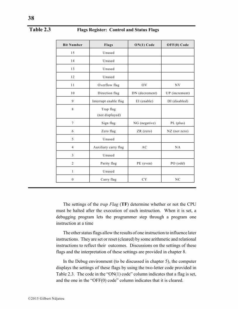
Flags Register
Bits positions in the 8086 processor’s Flags Register are named and used as
specified in Table 2.3.
The Direction flag (DF) is a control flag: it controls the direction of
string operations.
The Interrupt Enable flag (IF) is a system flag: It is used to control
maskable interrupts. By setting this flag, you allow the CPU to recognize
external (maskable) interrupts requests. Clearing it disables these interrupts.
Interrupts are discussed in a forthcoming section of this chapter.
The trap Flag (TF), Overflow flag (OF), Sign flag (SF), Zero flag (ZF),
Auxiliary Carry flag (AF), Parity flag, (PF), and the Carry flag (CF) are the
status flags.
38
©2015 Gilbert Ndjatou
Table 2.3 Flags Register: Control and Status Flags
Bit Number Flags ON(1) Code OFF(0) Code
15 Unused
14 Unused
13 Unused
12 Unused
11 Overflow flag OV NV
10 Direction flag DN (decrement) UP (increment)
9 Interrupt enable flag EI (enable) DI (disabled)
8 Trap flag
(not displayed)
7 Sign flag NG (negative) PL (plus)
6 Zero flag ZR (zero) NZ (not zero)
5 Unused
4 Auxiliary carry flag AC NA
3 Unused
2 Parity flag PE (even) PO (odd)
1 Unused
0 Carry flag CY NC
The settings of the trap Flag (TF) determine whether or not the CPU
must be halted after the execution of each instruction. When it is set, a
debugging program lets the programmer step through a program one
instruction at a time
The other status flags allow the results of one instruction to influence later
instructions. They are set or reset (cleared) by some arithmetic and relational
instructions to reflect their outcomes. Discussions on the settings of these
flags and the interpretation of these settings are provided in chapter 8.
In the Debug environment (to be discussed in chapter 5), the computer
displays the settings of these flags by using the two-letter code provided in
Table 2.3. The code in the “ON(1) code” column indicates that a flag is set,
and the one in the “OFF(0) code” column indicates that it is cleared.

39
©2015 Gilbert Ndjatou
Instruction Execution Cycle
The CPU executes a machine language instruction in three stages: It
performs the fetch operation in the first stage, the decode operation in the
second stage, and the execute operation in the third stage. These operations
are usually referred to as the fetch, decode, and execute cycle, as they are
continuously repeated for each instruction. They are described as follows:
! Fetch Operation: the CU computes the absolute address of the next
instruction to be executed by using the offset in the instruction pointer
register IP, and the segment selector in the code segment register CS. It
then fetches (copies) the instruction at that absolute address to a register
inside the CPU.
! Decode Operation: the control unit increments the instruction pointer
register IP by the size of the instruction just fetched, and then decodes
the instruction by interpreting its opcode. If other operands are specified
by the instruction, the control unit decodes their addresses and fetches the
operands. It then passes the instruction and its operands (if any) to the
arithmetic and logic unit for execution.
! Execute Operation: the arithmetic and logic unit executes the
instruction and passes the result to the control unit. The control unit then
returns the result to the register(s) or the main memory.
Exercise 2.3
Part I Fill in the blanks with the most appropriate answers.
1. The ________________________________________ controls the operations of the different
components of the system hardware and executes the instructions of a program.
2. The _________________________________ controls the operations of the different
components of a computer system hardware, supervises the transfer of data between the
components of the system, and fetches the instructions of a program from the main memory.
3. The __________________________ interprets (decodes) instructions, and then sends control
signals to the ALU to perform the operation specified by the instruction.
4. The ______________________________________________ performs the arithmetic,
relational, and logical operations on data.

40
©2015 Gilbert Ndjatou
5. A _____________________________ is a special high-speed memory location within the CPU
that are directly accessed by both the control unit and the arithmetic and logic unit.
6. ____________________________ registers are used to hold the operands of arithmetic and
logical instructions.
7. Registers ________________________________________________ are the only registers of
the Intel 8086 processor that may be used to specify the offset of a memory location operand
of an instruction.
8. A __________________________ register is used to hold the segment selector of a segment in
the main memory.
9. Register________________ holds the segment selector of the segment that contains the code
area.
10. Register ________________ holds the segment selector of the segment that contains the data
area.
11. Register _______________ holds the segment selector of the segment that contains the stack
area.
12. Register ___________ holds the segment selector of the segment that contains the extra data
area.
13. Register ___________holds the offset (in the code segment) of the next instruction to be
executed by the CPU.
14. The ______________________________ is a special register with individual bit settings used
to control certain operations, and to indicate the status of the 8086 processor.
Part II
1. What are the major components of the central processing unit (CPU) or processor?
2. What are the major functions of the Control Unit?
3. What are the major functions of the Arithmetic and Logic Unit?
4. What are the first processors used on IBM PC and compatible computers?
5. What are the processors used on most IBM PC and compatible computers today?
6. Do you need to add a math-coprocessor to an IBM PC with an Intel Pentium? Why?
7. The registers of the Intel 8086 processor may be grouped into three basic categories according
to the ways that they may be used. What are those categories?
8. Name the general-purpose registers of the Intel 8086 processor.
9. The bytes of some registers of the Intel 8086 processor are treated as a unit. Provide the names
of those registers, and the names of their bytes.

41
©2015 Gilbert Ndjatou
10. What are the four registers of the Intel 8086 processor that may be used to specify the offset of
memory location operands of instructions?
11. A machine language program of the Intel 8086 processor consists of up to four separate sections
or areas. Give the name of each of these areas and its contents.
12. The flags of a flag register are classified into three categories. Name these categories and also
provide the flags in each of these categories.
13. Describe the fetch, the decode, and the execute operations.
Part III Answer by True or False.
1. A register can only store a fixed size of data. True. False.
2. All computers have 16-bit registers. True. False.
3. Instructions with registers operands execute much faster than those with memory location
operands. True. False.
4. When you buy a computer, you can upgrade the number of registers in that computer.
True. False.
5. The Intel 8088 and 8086 processors were the first processors used on IBM PC and compatible
computers. True. False.
6. An Intel Pentium processor has two or more modes of operation such that in one of these modes
of operation, it behaves like an Intel 8086 processor. True. False.
7. All registers of an Intel 8086 processor may also be accessed as two separate 8-bit (1-byte)
registers. True. False.
8. When a program is loaded in memory, each of the program areas is placed in a (physical)
segment, and a segment register is used to hold the segment selector of that segment.
True. False.
9. A data segment of a program can be larger than 64 KB. True. False.
10. For most instructions, a memory location operand is specified by its offset in the segment in
which it is located. True. False.
11. In order to access data in a memory location, the CPU must first compute the physical address
of that memory location by using the offset specified in the instruction and the segment selector
in the corresponding segment register. True. False.
12. The sections (code, stack, data) of a machine language program may all be contained in the same
physical segment (frame). True. False.
42
©2015 Gilbert Ndjatou
2.3 Clock
The clock is a device within the computer that generates periodic signals that
are used to pace the operations of the CPU. The most basic unit of time for
the CPU is the clock cycle: The amount of time that is needed by the CPU to
execute an instruction is expressed in terms of clock cycles, and the speed of
the CPU is determined by the system clock rate (number of cycles per
second), the word size, and the bus width. The system clock rate is
measured in megahertz (MHz) which corresponds to one million cycles per
second. Intel 8086 processors had clock rates in the range of 5 MHz to 8
MHz. But today’s newer Intel Pentium processors have clock rates over 2.4
Ghz (gigahertz), with one gigahertz equal to one billion cycles per second.
Exercise 2.4
Fill in the blanks with the most appropriate answers.
1. The _______________________ is a device within the computer that generates periodic signals
that are used to pace the operations of the CPU.
2. The most basic unit of time for the CPU is the _______________________________________.
3. The amount of time that is needed by the CPU to execute an instruction is expressed in terms
of ___________________________________________________________________________.
4. The speed of the CPU is determined by the following: _______________________________
_____________________________________________________________________________.
5. The system clock rate is measured in _______________________________________________.
6. One megahertz (MHz) corresponds to _____________________________________ per second.

43
©2015 Gilbert Ndjatou
2.4 Input and Output Systems
The Input system consists of the input devices and their controllers. An
input device transmits information from the outside world to the computer.
Examples of input devices are keyboards, mice, joysticks, scanners,
terminals, microphones . . . etc.
The output system consists of the output devices and their controllers.
An output device transmits information from the computer to the outside
world. Examples of output devices are printers, monitors, plotters, speakers,
terminals, . . ., etc.
Controllers are located between the CPU and the input/output devices,
and there is a controller for each device. For an output device, a controller
accepts data from the computer that it converts into signals used by that
device. For an input device, it accepts signals from the device that it converts
into sequences of bits to be used inside the computer.
On IBM PC and compatible computers, controllers often take the form of
a printed circuit board that can be inserted into the motherboard or an
expansion slot. There are also controllers than can handle two, four, or even
more identical devices.
Each controller has special registers (usually a byte or a word) for
communication with the CPU. In some computers such as those based on
Motorola 680x0 processors, these registers are part of the memory address
space: they are given addresses in the same range of addresses as the ones
given to bytes in the main memory. This approach is usually referred to as
memory-mapped input/output. In computers based on Intel processors,
these registers are referred to as ports, and a typical controller may have three
or more ports associated with it as follows:
! A control port is used to set control information such as the send
or the receive information.
! A data port is used to hold the data to be transmitted or the
data received.
! A status port is used to record information about the status of
the controller or the device.

44
©2015 Gilbert Ndjatou
Figure 2.3 Some 8086 I/O Controllers and their I/O Addresses and Interrupts
I/O Controller I/O Address Interrupt
Clock 040h - 05Fh 1Ch
Keyboard 060h - 060h 9h
Hard Disk 1F0h - 1F7h 76h
Serial Port Controller COM1 3F8h - 3FFh Bh
Serial Port Controller COM2 2F8h - 2FFh Ch
Printer (LPT1) 378h - 37Fh Fh
Floppy Disk 3F0h - 3F5h Eh
Each controller has at least a data port, but the functions of the status and
the control ports may be combined into one port for a simple controller.
Sophisticated controllers may however have several control and status ports.
The port (or I/O) address space is separate from the memory address space.
The port addresses available for the Intel 8086 processor based computers
are 000h - 3FFh. Each controller is allocated a certain range of this address
space to identify its ports as shown in Figure 2.3. While the actual port
numbers and port settings may differ from machine to machine, the
techniques involved are the same. Today’s Intel processors have port
addresses in the range 0000h - FFFFh.
Controllers also use interrupts (discussed later in this chapter) to
communicate with the CPU.

45
©2015 Gilbert Ndjatou
Exercise 2.5
Part I Fill in the blanks with the most appropriate answers.
1. The Input system consists of the ______________________ and _______________________.
2. An _______________________ transmits information from the outside world to the computer.
3. The output system consists of the _____________________ and _________________________.
4. An ________________________ transmits information from the computer to the outside world.
Part II
1. Provide four examples of input devices.
2. Provide four examples of output devices.
3. What are the three types of registers found in most controllers?
4. What are the major functions of an input controller?
5. What are the major functions of an output controller?
6. What is the major difference between the controllers of a Motorola 68x0 processor and those
of an Intel processor?
7. How does a controller communicate with the CPU?
2.5 Secondary Storage
Since the RAM is volatile, data and programs (in the RAM) that are needed
for future use in the computer must be permanently saved in a different type
of memory before the computer is turned off. This type of memory is
referred to as secondary storage (or memory). Examples of secondary
storage are floppy disks, hard disks, tapes and CD ROMs.
In order to use a particular secondary storage on a computer, that
computer must be equipped with a hardware device called drive to read
and/or write on that secondary memory. For example, in order to use a
floppy disk on an IBM PC, that computer must be equipped with a floppy
disk drive.
46
©2015 Gilbert Ndjatou
A controller is also needed for communication between the CPU and
each drive. Figure 2.1 shows how drives and their controllers are connected
to the rest of the computer system, and Figure 2.3 provides the I/O address
and the interrupt information for the floppy disk drive and the hard disk drive
controllers of a computer system based on the Intel 8086 processor.
Exercise 2.6
1. Why do you need a secondary storage device on a computer system?
2. What is needed on a computer system for a particular secondary storage to be used on it?
3. Describe the functions of a floppy disk controller.
2.6 System Interconnection
The transfer of data from one component of the computer system to another,
and the sending of control codes and other signals by the CPU to the
controllers or the memory control unit are accomplished by using a set of
parallel wires referred to as the system bus. It consists of the data bus, the
address bus, and the control bus as illustrated in Figure 2.4.
The data bus is used for the flow of data between the different
components of the system, whereas the address bus is used by the CPU to
specify the address of the memory location or the controller’s register being
accessed. The control bus or control lines is used by the CPU to send
control signals to controllers or the memory control unit.
Computers that use the Intel 8086 processor have a 20-bit wide address
bus: one wire for each bit of the physical address. The data bus is 16 bits
wide.

47
©2015 Gilbert Ndjatou
Sending and Receiving Data
To write a word of data to a memory location, the processor puts the address
of that memory location onto the address bus, and the data to be sent onto the
data bus; it then puts the command to write to memory onto the control bus.
The memory control unit then decodes the command and the address,
retrieves the data from the data bus, and stores it into the corresponding
memory location.
To output data to a controller’s data port, the processor puts the
corresponding port address onto the address bus, and the data to be sent onto
the data bus; it then puts the command to output data onto the control bus.
The controller being addressed is responsible for recognizing the output
command and the port address, and for retrieving the data from the data bus.
To read from a memory location, the processor puts the address of that
memory location onto the address bus, and the command to read from
memory onto the control bus. The memory control unit is responsible for
decoding the address, retrieving the data from the appropriate memory
location, and placing it onto the data bus for retrieval by the CPU.
To input data from a controller’s data port, the CPU puts the
corresponding port address onto the address bus, and the command to input
data onto the control bus. The controller being addressed recognizes the
input data command and then decodes the port address as the address of one
of its data registers. It then retrieves the data from the register and places it
onto the data bus where it is retrieved by the CPU.
Note that after the CPU has put an address onto the address bus and a
command onto the control bus, All the devices connected to the system bus
and the memory control unit see this address and the command
simultaneously, but only the addressed unit (memory control unit or device)
responds to it.

48
©2015 Gilbert Ndjatou
Processor Controller ControllerMemory
Control Unit
DriveI/ODevice
Memory
Figure 2.4 Bus System of Intel X86 Processors Based Computer Systems
Address Bus
Data Bus
Control Bus
Exercise 2.7
1. Describe the system bus of a computer system with the Intel 8086 processor.
2. Describe the process used by the Intel 8086 processor to perform each of the following
operations:
a. read data from the main memory. c. write data to the main memory.
b. read data from the keyboard. d. send data to the printer.

49
©2015 Gilbert Ndjatou
2.7 Interrupts
An interrupt is a signal to the CPU that an event that needs immediate
attention has occurred. The CPU responds to an interrupt by suspending the
program being executed, and then transferring control to a special program
in the memory called interrupt handler. Depending on the cause of an
interrupt, the control of the CPU may or may not be returned to the suspended
program at the end of the interrupt handler.
There are two types of interrupts: hardware/external interrupts and
software/internal interrupts.
An external interrupt is initiated outside of the CPU by hardware
devices such as the clock and controllers. For example, an input device
controller may generate an interrupt to alert the CPU that the transfer of data
requested by the CPU is completed. Some events such as power failure or
operator-initiated system shutdown also generate external interrupts.
An internal interrupt is generated within the CPU by errors detected
during the execution of an instruction or by some instructions that are
specifically designed to initiate interrupts. Some error-initiated interrupts are
caused by overflow conditions, attempt to divide by 0, invalid operation code
(opcode) or data, or an attempt to access memory locations outside of the
region allocated to a program in a multiprogramming system.
Intel 8086 Processor’s Interrupts
The Intel 8086 processor may recognize 256 different interrupts. Each of
these interrupts is identified by an 8-bit number (00h - FFh) called interrupt
type. To each interrupt is also associated a special program in the memory
called interrupt handler. The interrupt handler associated with an interrupt
is executed by the CPU each time that interrupt occurs.
Memory locations from physical address 00000h to 003FFh (1024 bytes)
are used to hold the segment selector:offest addresses of the interrupt
handlers in such a way that the segment selector:offset address of the
interrupt handler for interrupt type N is at physical address 4 x N:

50
©2015 Gilbert Ndjatou
the segment selector:offest address of the interrupt handler for interrupt
type 00h is at physical address 4 x 0 = 00000h;
that of interrupt type 01h is at physical address 4 x 1 = 00004h, . . . , and
that of interrupt type FFh is at physical address 4 x FF = 003FCh.
In other words, the interrupt handler of interrupt type N is somewhere in the
main memory, but its segment selector:offset address is placed at physical
address 4xN.
The segment selector:offset address of an interrupt handler is called
interrupt vector. It is stored in memory in the format <offset><selector>
with the bytes of both the offset and the selector swapped. So, if 4E01 0F1A
is an interrupt vector, then the corresponding offset and segment selector are
respectively 014E and 1A0F.
Exercise 2.8
1. What is an interrupt?
2. How does the CPU respond to an interrupt?
3. What is the difference between an internal interrupt and an external interrupt?
4. What are the segment selector and the offset that correspond to the interrupt vector
4A02 01C5
5. Compute the physical address of the memory location that contains the segment selector: offset
address of the interrupt handler for each of the following interrupts
a. interrupt 7 b. interrupt 10h c. interrupt 2C

51
©2015 Gilbert Ndjatou
Chapter 2: Exercises
1. Describe the functions of each of the four major components of a digital computer system
hardware?
2. What is the size of each of the following memory units in an Intel 8086 processor based
computer system?
a. Byte b. word c. doubleword d. quadword;
3. What is a paragraph?
4. What is the maximum size of a segment?
5. What is a paragraph boundary? Give an example of a paragraph boundary.
6. What does the segment selector of a segment represent? What does the offset of a byte in a
segment represent?
7. Compute the 20-bit absolute address that corresponds to each of the following segment selector:
offset addresses:
a. 3A50 : 00B7 b. 42F5 : 123E c. 6443 : 3101 d. 0010 : AF25.
8. Do the following for each of the following physical addresses:
i) determine the offset needed to access the corresponding byte in the segment with segment
selector 1200.
ii) determine the offset needed to access the corresponding byte in the segment with segment
selector 10F5.
a. 12A50 b. 1B4F9 c. 138EE d. 1480F
9. What is the canonic frame number for each of the following physical addresses:
a. 247A0; b. 5F039 c. 56321 d. A4E44.
10. What is the offset that corresponds to each of the canonic frame numbers in question 9?
11. What are the three major components of a processor?
12. What are the major functions of the control unit.
13. Name the four areas of a machine language program with their contents.
14. Name the segment registers of an Intel 8086 processor with their contents.
15. What is the instruction pointer register used for?
16. What are the three things that determine the speed of the CPU?

52
©2015 Gilbert Ndjatou
17. What is the clock rate of most Intel Pentium processors today?
18. What are the major function of an input controller?
19. What are the major function of an output controller?
20. What is the major difference between the controllers used on Motorola processors 680x0-based
computers and those used on computers with Intel processors?
21. What are the different types of port that a controller in an Intel processor based computer system
may have?