Chapter 15 Transformer Design - University of Colorado...
40
Fundamentals of Power Electronics Chapter 15: Transformer design 1 Chapter 15 Transformer Design Some more advanced design issues, not considered in previous chapter: • Inclusion of core loss • Selection of operating flux density to optimize total loss • Multiple winding design: as in the coupled-inductor case, allocate the available window area among several windings • A transformer design procedure • How switching frequency affects transformer size n 1 : n 2 : n k R 1 R 2 R k + v 1 (t) – + v 2 (t) – + v k (t) – i 1 (t) i 2 (t) i k (t)
Transcript of Chapter 15 Transformer Design - University of Colorado...

Fundamentals of Power Electronics Chapter 15: Transformer design1
Chapter 15 Transformer Design
Some more advanced design issues, not considered in previous
chapter:
• Inclusion of core loss
• Selection of operating flux
density to optimize total loss
• Multiple winding design: as in
the coupled-inductor case,
allocate the available window
area among several windings
• A transformer design
procedure
• How switching frequency
affects transformer size
n1 : n2
: nk
R1 R2
Rk
+
v1(t)
–
+
v2(t)
–
+
vk(t)
–
i1(t)i2(t)
ik(t)

Fundamentals of Power Electronics Chapter 15: Transformer design2
Chapter 15 Transformer Design
15.1 Transformer design: Basic constraints
15.2 A step-by-step transformer design procedure
15.3 Examples
15.4 AC inductor design
15.5 Summary

Fundamentals of Power Electronics Chapter 15: Transformer design3
15.1 Transformer Design:Basic Constraints
Core loss
Typical value of for ferrite materials: 2.6 or 2.7
B is the peak value of the ac component of B(t), i.e., the peak ac flux
density
So increasing B causes core loss to increase rapidly
This is the first constraint
Pfe = K fe(∆B)β Ac lm

Fundamentals of Power Electronics Chapter 15: Transformer design4
Flux densityConstraint #2
Flux density B(t) is related to the
applied winding voltage according
to Faraday’s Law. Denote the volt-
seconds applied to the primary
winding during the positive portionof v1(t) as 1:
λ1 = v1(t)dtt1
t2
This causes the flux to change from
its negative peak to its positive peak.
From Faraday’s law, the peak value
of the ac component of flux density is
To attain a given flux density,
the primary turns should be
chosen according to
area λ1
v1(t)
t1 t2 t
∆B =λ1
2n1Acn1 =
λ1
2∆BAc

Fundamentals of Power Electronics Chapter 15: Transformer design5
Copper lossConstraint #3
• Allocate window area between windings in optimum manner, as
described in previous section
• Total copper loss is then equal to
Pcu =ρ(MLT)n1
2I tot2
WAKuItot =
n j
n1I jΣ
j = 1
k
with
Eliminate n1, using result of previous slide:
Note that copper loss decreases rapidly as B is increased
Pcu =ρλ1
2 I tot2
4Ku
(MLT )WAAc
21∆B
2

Fundamentals of Power Electronics Chapter 15: Transformer design6
Total power loss4. Ptot = Pcu + Pfe
Ptot = Pfe + Pcu
There is a value of B
that minimizes the total
power loss
Pcu =ρλ1
2 I tot2
4Ku
(MLT )WAAc
21∆B
2
Pfe = K fe(∆B)β Ac lm∆B
Powerloss
Ptot
Copper loss P
cu
Cor
e lo
ss P
fe
Optimum ∆B
Fundamentals of Power Electronics Chapter 15: Transformer design7
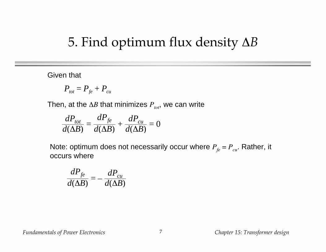
5. Find optimum flux density B
Ptot = Pfe + Pcu
Given that
Then, at the B that minimizes Ptot, we can write
Note: optimum does not necessarily occur where Pfe = Pcu. Rather, itoccurs where
dPtot
d(∆B)=
dPfe
d(∆B)+
dPcu
d(∆B)= 0
dPfe
d(∆B)= –
dPcu
d(∆B)

Fundamentals of Power Electronics Chapter 15: Transformer design8
Take derivatives of core and copper loss
Now, substitute into and solve for B:
Optimum B for a
given core and
application
Pcu =ρλ1
2 I tot2
4Ku
(MLT )WAAc
21∆B
2Pfe = K fe(∆B)β Ac lm
dPfe
d(∆B)= βK fe(∆B) β – 1 Aclm dPcu
d(∆B)= – 2
ρλ12I tot
2
4Ku
(MLT)WAAc
2 (∆B)– 3
dPfe
d(∆B)= –
dPcu
d(∆B)
∆B =ρλ1
2I tot2
2Ku
(MLT )WAAc
3lm
1βK fe
1β + 2

Fundamentals of Power Electronics Chapter 15: Transformer design9
Total loss
Substitute optimum B into expressions for Pcu and Pfe. The total loss is:
Rearrange as follows:
Left side: terms depend on core
geometry
Right side: terms depend on
specifications of the application
Ptot = AclmK fe
2β + 2
ρλ12I tot
2
4Ku
(MLT )WAAc
2
ββ + 2 β
2
–β
β + 2+
β2
2β + 2
WA Ac2(β – 1)/β
(MLT )lm2/β
β2
–β
β + 2+
β2
2β + 2
–β + 2β
=ρλ1
2I tot2 K
fe
2/β
4Ku Ptotβ + 2 /β

Fundamentals of Power Electronics Chapter 15: Transformer design10
The core geometrical constant Kgfe
Define
Design procedure: select a core that satisfies
Appendix D lists the values of Kgfe for common ferrite cores
Kgfe is similar to the Kg geometrical constant used in Chapter 14:
• Kg is used when Bmax is specified
• Kgfe is used when B is to be chosen to minimize total loss
Kgfe =WA Ac
2(β – 1)/β
(MLT)lm2/β
β2
–β
β + 2+
β2
2β + 2
–β + 2β
Kgfe ≥ρλ1
2I tot2 K
fe
2/β
4Ku Ptotβ + 2 /β

Fundamentals of Power Electronics Chapter 15: Transformer design11
15.2 Step-by-steptransformer design procedure
The following quantities are specified, using the units noted:Wire effective resistivity ( -cm)
Total rms winding current, ref to pri Itot (A)
Desired turns ratios n2/n1, n3/n1, etc.
Applied pri volt-sec 1 (V-sec)
Allowed total power dissipation Ptot (W)
Winding fill factor Ku
Core loss exponent
Core loss coefficient Kfe (W/cm3T )
Other quantities and their dimensions:Core cross-sectional area Ac (cm2)
Core window area WA (cm2)
Mean length per turn MLT (cm)
Magnetic path length le (cm)
Wire areas Aw1, … (cm2)
Peak ac flux density B (T)

Fundamentals of Power Electronics Chapter 15: Transformer design12
Procedure1. Determine core size
Select a core from Appendix D that satisfies this inequality.
It may be possible to reduce the core size by choosing a core materialthat has lower loss, i.e., lower Kfe.
Kgfe ≥ρλ1
2I tot2 K
fe
2/β
4Ku Ptotβ + 2 /β
108

Fundamentals of Power Electronics Chapter 15: Transformer design13
2. Evaluate peak ac flux density
At this point, one should check whether the saturation flux density isexceeded. If the core operates with a flux dc bias Bdc, then B + Bdcshould be less than the saturation flux density Bsat.
If the core will saturate, then there are two choices:
• Specify B using the Kg method of Chapter 14, or
• Choose a core material having greater core loss, then repeat
steps 1 and 2
∆B = 108 ρλ12I tot
2
2Ku
(MLT )WAAc
3lm
1βK fe
1β + 2

Fundamentals of Power Electronics Chapter 15: Transformer design14
3. and 4. Evaluate turns
Primary turns:
Choose secondary turns according to
desired turns ratios:
n2 = n1
n2
n1
n3 = n1
n3
n1
n1 =λ1
2∆BAc
104

Fundamentals of Power Electronics Chapter 15: Transformer design15
5. and 6. Choose wire sizes
α1 =n1I1
n1I tot
α2 =n2I2
n1I tot
αk =nkIk
n1I tot
Fraction of window area
assigned to each winding:Choose wire sizes according
to:
Aw1 ≤α1KuWA
n1
Aw2 ≤α2KuWA
n2

Fundamentals of Power Electronics Chapter 15: Transformer design16
Check: computed transformer model
iM , pk =λ1
2LM
R1 =ρn1(MLT)
Aw1
R2 =ρn2(MLT)
Aw2
Predicted magnetizing
inductance, referred to primary:
Peak magnetizing current:
Predicted winding resistances:
n1 : n2
: nk
R1 R2
Rk
i1(t) i2(t)
ik(t)
LM
iM(t)
L M =µn1
2Ac
lm

Fundamentals of Power Electronics Chapter 15: Transformer design17
15.4.1 Example 1: Single-output isolatedCuk converter
100 W fs = 200 kHz
D = 0.5 n = 5
Ku = 0.5 Allow Ptot = 0.25 W
Use a ferrite pot core, with Magnetics Inc. P material. Loss
parameters at 200 kHz are
Kfe = 24.7 = 2.6
+–
+
V5 V
–
Vg
25 V
n : 1
I20 A
Ig
4 A
+
v2(t)
–
–
v1(t)
+
i1(t) i2(t)
– vC2(t) ++ vC1(t) –

Fundamentals of Power Electronics Chapter 15: Transformer design18
Waveforms
v1(t)
i1(t)
i2(t)
DTs
Area λ1VC1
– nVC2
D'Ts
I/n
– Ig
I
– nIg
Applied primary volt-
seconds:
λ1 = DTsVc1 = (0.5) (5 µsec ) (25 V)= 62.5 V–µsec
Applied primary rms
current:
I1 = D In
2
+ D' Ig2 = 4 A
Applied secondary rms
current:I2 = nI1 = 20 A
Total rms winding
current:
I tot = I1 + 1n I2 = 8 A

Fundamentals of Power Electronics Chapter 15: Transformer design19
Choose core size
Kgfe ≥(1.724⋅10– 6)(62.5⋅10– 6)2(8)2(24.7) 2/2.6
4 (0.5) (0.25) 4.6/2.6108
= 0.00295
Pot core data of Appendix D lists 2213 pot core with
Kgfe = 0.0049
Next smaller pot core is not large enough.

Fundamentals of Power Electronics Chapter 15: Transformer design20
Evaluate peak ac flux density
This is much less than the saturation flux density of approximately0.35 T. Values of B in the vicinity of 0.1 T are typical for ferrite
designs that operate at frequencies in the vicinity of 100 kHz.
∆B = 108 (1.724⋅10– 6)(62.5⋅10– 6)2(8)2
2 (0.5)(4.42)
(0.297)(0.635)3(3.15)1
(2.6)(24.7)
1/4.6
= 0.0858 Tesla

Fundamentals of Power Electronics Chapter 15: Transformer design21
Evaluate turns
n1 = 104 (62.5⋅10– 6)2(0.0858)(0.635)
= 5.74 turns
n2 =n1
n = 1.15 turns
In practice, we might select
n1 = 5 and n2 = 1
This would lead to a slightly higher flux density and slightly higher
loss.

Fundamentals of Power Electronics Chapter 15: Transformer design22
Determine wire sizes
Fraction of window area allocated to each winding:
α1 =4 A
8 A= 0.5
α2 =15 20 A
8 A= 0.5
(Since, in this example, the ratio of
winding rms currents is equal to the
turns ratio, equal areas are
allocated to each winding)
Wire areas:
Aw1 =(0.5)(0.5)(0.297)
(5)= 14.8⋅10– 3 cm2
Aw2 =(0.5)(0.5)(0.297)
(1)= 74.2⋅10– 3 cm2
From wire table,
Appendix D:
AWG #16
AWG #9

Fundamentals of Power Electronics Chapter 15: Transformer design23
Wire sizes: discussion
Primary
5 turns #16 AWG
Secondary
1 turn #9 AWG
• Very large conductors!
• One turn of #9 AWG is not a practical solution
Some alternatives
• Use foil windings
• Use Litz wire or parallel strands of wire

Fundamentals of Power Electronics Chapter 15: Transformer design24
Effect of switching frequency on transformer sizefor this P-material Cuk converter example
0
0.02
0.04
0.06
0.08
0.1
Switching frequency
Bm
ax , TeslaP
ot c
ore
size
4226
3622
2616
2213
1811 1811
2213
2616
25 kHz 50 kHz 100 kHz 200 kHz 250 kHz 400 kHz 500 kHz 1000 kHz
• As switching frequency is
increased from 25 kHz to
250 kHz, core size is
dramatically reduced
• As switching frequency is
increased from 400 kHz to
1 MHz, core size
increases

Fundamentals of Power Electronics Chapter 15: Transformer design25
15.3.2 Example 2Multiple-Output Full-Bridge Buck Converter
Switching frequency 150 kHz
Transformer frequency 75 kHz
Turns ratio 110:5:15
Optimize transformer at D = 0.75
: n2
+
v1(t)
–
+–
D1
Q1
D2Q2
D3
Q3
D4Q4
i1(t)
+
5 V
–
D5
D6
I5V
100 Ai2a(t)
+
15 V
–
D7
D8
i3a(t)
n1 :
: n2
: n3
: n3
i2b(t)
i2b(t)
I15V
15 A
T1
Vg
160 V

Fundamentals of Power Electronics Chapter 15: Transformer design26
Other transformer design details
Use Magnetics, Inc. ferrite P material. Loss parameters at 75 kHz:
Kfe = 7.6 W/T cm3
= 2.6
Use E-E core shape
Assume fill factor of
Ku = 0.25 (reduced fill factor accounts for added insulation required
in multiple-output off-line application)
Allow transformer total power loss of
Ptot = 4 W (approximately 0.5% of total output power)
Use copper wire, with
= 1.724·10–6 -cm

Fundamentals of Power Electronics Chapter 15: Transformer design27
Applied transformer waveforms
t
i2a(t)
0
i3a(t)
0 DTs Ts 2TsTs+DTs
i1(t)
0
v1(t)
0 0
Vg
– Vg
Area λ1
= Vg DTs
n2
n1
I5V +n3
n1
I15V
–n2
n1
I5V +n3
n1
I15V
I5V0.5I5V
I15V0.5I15V
0
: n2
+
v1(t)
–
D3
D4
i1(t)
D5
D6
i2a(t)
D7
D8
i3a(t)
n1 :
: n2
: n3
: n3
i2b(t)
i2b(t)
T1

Fundamentals of Power Electronics Chapter 15: Transformer design28
Applied primary volt-seconds
v1(t)
0 0
Vg
– Vg
Area λ1
= Vg DTs
λ1 = DTsVg = (0.75) (6.67 µsec ) (160 V) = 800 V–µsec

Fundamentals of Power Electronics Chapter 15: Transformer design29
Applied primary rms current
i1(t)
0
n2
n1
I5V +n3
n1
I15V
–n2
n1
I5V +n3
n1
I15V
I1 =n2n1
I5V +n3n1
I15V D = 5.7 A

Fundamentals of Power Electronics Chapter 15: Transformer design30
Applied rms current, secondary windings
t
i2a(t)
0
i3a(t)
0 DTs Ts 2TsTs+DTs
I5V0.5I5V
I15V0.5I15V
0
I3 = 12 I15V 1 + D = 9.9 A
I2 = 12 I5V 1 + D = 66.1 A

Fundamentals of Power Electronics Chapter 15: Transformer design31
Itot
RMS currents, summed over all windings and referred to primary
I tot =n j
n1I jΣ
all 5windings
= I1 + 2n2n1
I2 + 2n3n1
I3
= 5.7 A + 5110
66.1 A + 15110
9.9 A
= 14.4 A

Fundamentals of Power Electronics Chapter 15: Transformer design32
Select core size
Kgfe ≥(1.724⋅10– 6)(800⋅10– 6)2(14.4)2(7.6) 2/2.6
4 (0.25) (4) 4.6/2.6108
= 0.00937
A
From Appendix D
Fundamentals of Power Electronics Chapter 15: Transformer design33
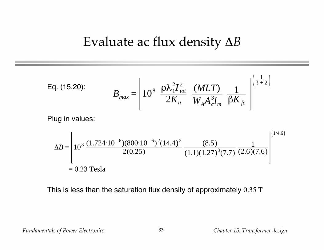
Evaluate ac flux density B
Bmax = 108 ρλ12I tot
2
2Ku
(MLT)WAAc
3lm
1βK fe
1β + 2
Eq. (15.20):
Plug in values:
This is less than the saturation flux density of approximately 0.35 T
∆B = 108 (1.724⋅10– 6)(800⋅10– 6)2(14.4)2
2(0.25)(8.5)
(1.1)(1.27)3(7.7)1
(2.6)(7.6)
1/4.6
= 0.23 Tesla

Fundamentals of Power Electronics Chapter 15: Transformer design34
Evaluate turns
Choose n1 according to Eq. (15.21):
n1 = 104 (800⋅10– 6)2(0.23)(1.27)
= 13.7 turns
Choose secondary turns
according to desired turns ratios:
n2 =5
110n1 = 0.62 turns
n3 =15
110n1 = 1.87 turns
Rounding the number of turns
To obtain desired turns ratio
of
110:5:15
we might round the actual
turns to
22:1:3
Increased n1 would lead to
• Less core loss
• More copper loss
• Increased total loss
n1 =λ1
2∆BAc
104

Fundamentals of Power Electronics Chapter 15: Transformer design35
Loss calculationwith rounded turns
With n1 = 22, the flux density will be reduced to
The resulting losses will be
Pfe = (7.6)(0.143)2.6(1.27)(7.7) = 0.47 W
Pcu =(1.724⋅10– 6)(800⋅10– 6)2(14.4)2
4 (0.25)(8.5)
(1.1)(1.27)21
(0.143)2 108
= 5.4 W
Ptot = Pfe + Pcu = 5.9 W
Which exceeds design goal of 4 W by 50%. So use next larger core
size: EE50.
∆B =(800⋅10– 6)2(22)(1.27)
104 = 0.143 Tesla

Fundamentals of Power Electronics Chapter 15: Transformer design36
Calculations with EE50
Repeat previous calculations for EE50 core size. Results:
B = 0.14 T, n1 = 12, Ptot = 2.3 W
Again round n1 to 22. Then
B = 0.08 T, Pcu = 3.89 W, Pfe = 0.23 W, Ptot = 4.12 W
Which is close enough to 4 W.

Fundamentals of Power Electronics Chapter 15: Transformer design37
Wire sizes for EE50 design
Aw1 =α1KuWA
n1
=(0.396)(0.25)(1.78)
(22)= 8.0⋅10– 3 cm2
⇒ AWG #19
Aw2 =α2KuWA
n2
=(0.209)(0.25)(1.78)
(1)= 93.0⋅10– 3 cm2
⇒ AWG #8
Aw3 =α3KuWA
n3
=(0.094)(0.25)(1.78)
(3)= 13.9⋅10– 3 cm2
⇒ AWG #16
α1 =I1
I tot
= 5.714.4
= 0.396
α2 =n2I2
n1I tot
= 5110
66.114.4
= 0.209
α3 =n3I3
n1I tot
= 15110
9.914.4
= 0.094
Window allocations Wire gauges
Might actually use foil or Litz wire for secondary windings

Fundamentals of Power Electronics Chapter 15: Transformer design38
Discussion: Transformer design
• Process is iterative because of round-off of physical number of
turns and, to a lesser extent, other quantities
• Effect of proximity loss
– Not included in design process yet
– Requires additional iterations
• Can modify procedure as follows:
– After a design has been calculated, determine number of layers in
each winding and then compute proximity loss
– Alter effective resistivity of wire to compensate: define
eff = Pcu/Pdc where Pcu is the total copper loss (including proximity
effects) and Pdc is the copper loss predicted by the dc resistance.
– Apply transformer design procedure using this effective wire
resistivity, and compute proximity loss in the resulting design.
Further iterations may be necessary if the specifications are not
met.
Fundamentals of Power Electronics Chapter 15: Transformer design39
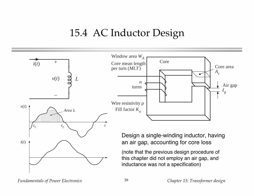
15.4 AC Inductor Design
+
v(t)
–
L
i(t) CoreWindow area WA
Core mean lengthper turn (MLT )
Wire resistivity ρFill factor Ku
Air gaplg
nturns
Core areaAc
Area λv(t)
t1 t2 t
i(t)
Design a single-winding inductor, having
an air gap, accounting for core loss
(note that the previous design procedure of
this chapter did not employ an air gap, andinductance was not a specification)

Fundamentals of Power Electronics Chapter 15: Transformer design40
Outline of key equations
L =µ0Acn2
lg
∆B = λ2nAc
Obtain specified inductance:
Relationship between
applied volt-seconds and
peak ac flux density:
Pcu =ρn2(MLT )
KuWAI 2
Copper loss (using dc
resistance):
∆B =ρλ2I 2
2Ku
(MLT )WAAc
3lm
1βK fe
1β + 2
Total loss is minimized when
Kgfe ≥ρλ2I 2K
fe
2/β
2Ku Ptotβ + 2 /β
Must select core that satisfies
See Section 15.4.2 for step-by-step
design equations