Chapter 14spikelab/papers/book01.pdf · Chapter 14 LASER FORWARD TRANSFER OF ELECTRONIC AND POWER...
35
Chapter 14 LASER FORWARD TRANSFER OF ELECTRONIC AND POWER GENERATING MATERIALS Alberto Piqué 1 , Heungsoo Kim 1 and Craig B. Arnold 2 1 U.S. Naval Research Laboratory, Washington DC; 2 Dept. of Mechanical and Aerospace Engineering, Princeton University, Princeton, NJ. 1. INTRODUCTION The application of laser forward transfer techniques has steadily grown since the first reports of patterned copper deposition by Bohandy, et al. 20 years ago (Bohandy, 1986). These general techniques employ a pulsed laser to locally transfer material from a source film onto a substrate in close proximity or in contact with the film. The source is typically a coated laser- transparent substrate, referred to as the target, donor, or ribbon. Laser pulses propagate through the transparent ribbon until they are absorbed by the film. Above an incident laser energy threshold, material is ejected from the film and transferred toward the acceptor, waiting or receiving substrate. These laser forward transfer techniques, known as laser direct-write (LDW), belong to a class of processes capable of generating a high-resolution pattern without the need for lithogaphic processes afterwards. Other examples of laser direct-write techniques include pyrolitic or photolytic decomposition of gas- or liquid-phase precursors, also known as laser CVD or laser-assisted deposition (Osgood, 1985; Herman, 1989). However, these non-forward transfer techniques will not be discussed in this chapter because they are not ablative in nature. Translation of the ribbon and receiving substrate, and/or scanning and modulating the laser beam enables complex pattern formation. Commercially available, computer-controlled translation stages or galvonometric scanning mirrors enable high-resolution patterns from the individually written 3D pixels or voxels resulting from the laser forward
Transcript of Chapter 14spikelab/papers/book01.pdf · Chapter 14 LASER FORWARD TRANSFER OF ELECTRONIC AND POWER...

Chapter 14
LASER FORWARD TRANSFER OF ELECTRONIC AND POWER GENERATING MATERIALS
Alberto Piqué1, Heungsoo Kim1 and Craig B. Arnold2
1U.S. Naval Research Laboratory, Washington DC; 2Dept. of Mechanical and Aerospace Engineering, Princeton University, Princeton, NJ.
1. INTRODUCTION
The application of laser forward transfer techniques has steadily grown since the first reports of patterned copper deposition by Bohandy, et al. 20 years ago (Bohandy, 1986). These general techniques employ a pulsed laser to locally transfer material from a source film onto a substrate in close proximity or in contact with the film. The source is typically a coated laser-transparent substrate, referred to as the target, donor, or ribbon. Laser pulses propagate through the transparent ribbon until they are absorbed by the film. Above an incident laser energy threshold, material is ejected from the film and transferred toward the acceptor, waiting or receiving substrate. These laser forward transfer techniques, known as laser direct-write (LDW), belong to a class of processes capable of generating a high-resolution pattern without the need for lithogaphic processes afterwards. Other examples of laser direct-write techniques include pyrolitic or photolytic decomposition of gas- or liquid-phase precursors, also known as laser CVD or laser-assisted deposition (Osgood, 1985; Herman, 1989). However, these non-forward transfer techniques will not be discussed in this chapter because they are not ablative in nature.
Translation of the ribbon and receiving substrate, and/or scanning and modulating the laser beam enables complex pattern formation. Commercially available, computer-controlled translation stages or galvonometric scanning mirrors enable high-resolution patterns from the individually written 3D pixels or voxels resulting from the laser forward

340 Laser Ablation and its Applications transfer process. Fig. 1 shows a schematic illustrating the basic elements required for the LDW apparatus.
One may consider the LDW technique to be analogous to ink-jet deposition of functional materials without the constraints of a nozzle, and with the added benefits of laser processing, such as material modifications and micromachining. This added versatility in comparison to other printing methods enables LDW to find opportunities in fields ranging from metals and power generation materials to biological and soft condensed matter.
Figure 1. Schematic illustration of the setup used for laser direct-write.
This chapter will provide a brief overview of the laser forward transfer and LDW literature, with a particular emphasis towards its application in electronic materials, followed by a more detailed review of LDW for the fabrication of micropower systems such as ultracapacitors, microbatteries and dye-sensitized solar cells. Finally, the chapter concludes with a discussion of the role that the LDW technique may play in the future of microelectronic manufacturing and other applications.
2. BACKGROUND
In order to discuss the recent developments in LDW of electronic and power generating materials for microelectronic applications, it is necessary to begin with an overview of the original work performed in laser forward transfer of the late 1980’s.

14. Laser Forward Transfer of Electronic and Power Generating... 341 2.1 Laser Induced Forward Transfer
The laser forward transfer process was first used in depositing copper metal patterns inside a vacuum chamber (Bohandy, 1986). Excimer laser pulses ( = 193 nm, 15 ns) were focused with a cylindrical lens to a 25 mm long by 50 m wide line on a source substrate containing a thin copper film. The Cu was transferred to Si and fused silica substrates, where further examination revealed resistivities ranging between 3 to 50 times the value for bulk copper with adhesion behavior that passed the “tape test”. Bohandy’s group coined the term laser-induced forward transfer (LIFT) to denote the process and developed a model to describe how it worked. According to this model; (1) the laser pulse heats the interface of the film at the source substrate; (2) a resulting melt front propagates through the film until it reaches the free surface; (3) at about this time, the material at the interface is superheated beyond its boiling point until, (4) the resulting vapor induced pressure at the interface propels the molten film forward towards the acceptor substrate (Adrian, 1987). The same group then demonstrated that this process can be carried out in air, i.e. under atmospheric conditions, without the need for a vacuum (Bohandy, 1988).
The LIFT technique is simple and can be used with a wide variety of film materials, mainly metals such as Cu and Ag (Bohandy, 1988), Al (Schultze, 1991), W (Tóth, 1993; Kántor, 1994) and Cr (Zergioti, 1998a). Reports of LIFT for other materials such as Al2O3 (Greer, 1988), In2O3 (Zergioti, 1998a), and even high temperature superconductors (Fogarassy, 1989) are worth mentioning, although the quality of the transferred ceramics was not as good as those deposited by traditional film growth techniques. The thickness of the transferred film on the acceptor substrate can be adjusted by repetitive transfers from the ribbon. In a similar way, multilayer structures can be deposited. In general, to achieve uniform transfers with good morphology and spatial resolution on the acceptor substrate; (1) the thickness of the film on the ribbon should not exceed 100 nm; (2) the ribbon film should strongly absorb the laser wavelength in use; (3) the ribbon should be in contact or very close (~ 10’s of micrometers) to the acceptor substrate; and (4) the laser fluence should barely exceed the threshold fluence for removal of the film from the ribbon. This last parameter is very important in order to control the quality of the films, since too high fluences result in excessive explosive vaporization of the film affecting the morphology and resolution of the transfers, while too low fluences result in incomplete transfers.

342 Laser Ablation and its Applications 2.2 Development of the Laser Direct-write Process
Despite its successful application to the deposition of thin metal layers, the actual uses of the LIFT process are limited due to several shortcomings. In LIFT, metal films are required to be deposited on the ribbon by conventional vapor deposition techniques that require vacuum deposition and other expensive processes. Since these metal films tend to be very thin (a few hundred nanometers), the individual layers deposited by LIFT are similarly thin, thus limiting its application to lithographic mask repair and other niche areas. During LIFT, the melting and solidification of the transferred material results in the formation of interfaces between adjacent voxels, which can have deleterious effects in the electrical transport properties of the patterned structure being fabricated. Furthermore, the melting of the transferred material becomes a serious issue when LIFT is performed under atmospheric conditions, because most metals are easily oxidized when melted in air. Moreover, the rapid quenching of the metal voxels can result in high intrinsic stresses between the transferred metal and the substrate, ultimately leading to poor adhesion and delamination of the transferred layers. Finally, LIFT is not suited for the transfer of ceramics and other inorganic phases given the irreversible phase changes and decomposition that tend to be exhibited by these materials upon melting and solidification.
The above limitations explain why LIFT is not suitable for the laser transfer of complex, sensitive materials such as those found in electronic and power generation devices. In fact, this realization is underscored by the decline in the number of publications reporting on LIFT of metals and other inorganic materials that followed in the late nineties. Despite these shortcomings, the capability for laser transferring materials in patterned form is extremely important for many commercial, aerospace and military applications.
The first variation of the LIFT process to attempt to overcome these limitations employed multilayered films (Tolbert, 1993a). The multilayers are formed by depositing a thin laser-absorbing layer (usually a metal) on the transparent support, followed by a layer of the material to be transferred. During transfer, the laser pulse interacts with the absorbing layer, referred to as the dynamic release layer, causing it to vaporize in a similar manner as in LIFT. This confined layer forces the material in the second layer to be removed from the film and transferred to the acceptor substrate. The advantage of this approach is that it allows the transfer of materials for which the previously described LIFT process is not effective. For instance, this can include materials with weak absorption of the laser radiation, or materials that can be damaged by their interaction with the laser pulse. This

14. Laser Forward Transfer of Electronic and Power Generating... 343 variation on the LIFT process was originally intended for high speed laser color printing applications, and was called laser ablation transfer (Tolbert, 1993a). More recently this approach has been used for the laser direct-write of phosphor powders (Fitz-Gerald, 2000) and extremely laser sensitive materials such as DNA biomolecules (Fernández-Pradas, 2004; Serra, 2004).
The work by Tolbert using the dynamic release layer approach to LIFT, showed for the first time that the pulse duration has an effect on the transfer process. Their experiments indicated that picosecond laser pulses are more efficient in ablating the multilayered films than nanosecond pulses, with transfer laser fluence thresholds an order of magnitude smaller (Tolbert, 1993b). Since then, various reports on the use of femtosecond lasers for laser forward transfer have validated Tolbert’s results. Most of the applications of femtosecond LIFT have been related to the laser transfer of metals (Zergioti, 1998b; Papakonstantinou, 1999; Bähnisch, 2000). However, more recently, femtosecond LIFT has successfully been applied to the transfer of biological materials (Karaiskou, 2003; Zergioti, 2005).
A second variation on the LIFT process employs an organic precursor compound (palladium acetate) rather than a pure metal for transfer (Esrom, 1995). This is significant as it demonstrates the laser forward transfer process can take advantage of the photoinduced decomposition of a precursor at the ribbon/coating interface to propel the reminder of the film forward and create a metal pattern. By irradiating the transferred mixture with additional laser pulses, a very thin (< 100 nm) but grainy Pd coating is produced, on which a thicker metal layer can be obtained by electroless plating. In their paper, the authors consider the laser transfer and subsequent electroless metal plating as a two-step process enabling the selective deposition of metal patterns. However, their key contribution shows that the LIFT process can be used to deposit a precursor of the desired material, which once transferred can be further decomposed or processed into its final form.
More recently, the LIFT process has been adapted for the transfer of various materials in powder form mixed with an organic binder. Such mixtures or matrices are then applied as a uniform coating on the transparent donor substrate to form a ribbon. The advantage of this approach resides in the fact that the transfer of thicker films from the ribbon can be achieved at lower laser fluences than with LIFT of homogenous films. Furthermore, the composite film is transferred in its solid phase, thus avoiding the melting and re-condensation steps that take place in traditional LIFT. This modified LIFT approach has been used for the LDW of diamond nanopowders (Pimenov, 1995), ferroelectric (BaTiO3 and SrTiO3) and ferrite (Y3Fe5O12) micron sized powders (Piqué, 1999, 1999b), and carbon composite polymers for gas sensing elements (Piqué 2000a). A limitation of this approach for these
344 Laser Ablation and its Applications applications is that the adhesion of the transferred layers can be poor and the organic binder remains after the transfer, thus high temperature calcination steps are necessary to achieve dense layers. However, in many applications, dense layers are not required and the particular properties of the deposited films are ideal. As a further generalization, the idea of using an organic binder in the process can be applied to the direct transfer of rheological systems (Piqué, 2000b; Auyeung 2000). The realization that pastes, inks, suspensions, and sol-gel solutions can be deposited in patterns without physical or chemical modification during their transfer from the ribbon to the acceptor substrate, opened the door to a number of applications with a wider range of materials and formulations. Originally, this “wet” laser forward transfer technique was named matrix assisted pulsed laser evaporation direct-write (MAPLE-DW), in reference to the transfer of a loosely defined matrix comprising of powders or particles dispersed in a liquid. However, since the transfer process does not necessarily involve the evaporation of a matrix, this terminology has been discarded in favor of the less confusing laser direct-write or LDW.
3. LASER DIRECT-WRITE OF ELECTRONIC MATERIALS
The use of laser direct write for the deposition of high quality electronic materials requires the generation of structures comprising of multiple voxels, adjacent or on top of each other, that readily merge to form a single, continuous pattern. Electrical interconnects provide a perfect example of this requirement as heterogeneous interfaces between voxels can degrade the overall conductivity. By enabling the transferred material to remain fluid, adjacent voxels on the receiving substrate will merge into one continuous segment. Fig. 2 shows a simple schematic illustrating the basic steps on the laser direct-write of such rheological systems.
In reality, the process represents an important difference from prior LIFT technology as functional materials are deposited without direct vaporization, which could affect their desirable physical or chemical properties such as electrical conductivity, dielectric properties or electrochemical activity. As shown schematically in Fig. 2, for absorbing materials, a small region of the ink interacts with a low fluence (< 100 mJ/cm2) laser pulse causing a small amount of the ink to evaporate. As the resulting vapor expands, it generates shear forces that result in the ejection of a droplet from the film which is unaffected by the incident laser. The droplet is then propelled in jet-like fashion towards the receiving substrate, where it is deposited with its

14. Laser Forward Transfer of Electronic and Power Generating... 345 original rheological properties intact. The claim that most if not all of the transferred fluid does not interact with the laser pulse has been substantiated by the results obtained with transfers of extremely laser sensitive systems, such as buffer solutions containing biomaterials, proteins and living cells (Wu, 2001), or electrochemically sensitive materials discussed below (Arnold, 2004a).
Figure 2. Schematic representation of the steps involved in the forward transfer of rheological systems during the LDW process. (a) The laser pulse is absorbed in the ink layer adjacent to the transparent glass plate. (b) The absorbed energy causes vaporization to occur and (c) propel a droplet of ink forward from the film. (d) Finally, the droplet splashes down on the substrate.
Given the diverse nature and large number of parameters affecting the
LDW process, a simple model as the one described in the previous paragraph cannot be expected to completely explain its behavior. For instance, it is known that laser parameters such as fluence, pulse duration and wavelength play an important role in the LDW process. Additionally, ink parameters such as the composition of the ink in the ribbon, its thickness, viscosity, solids content, and solids particle size greatly affect the ability to transfer a particular fluid and the resulting morphology of the transferred voxels.
Parameters such as the distance between the ribbon and the receiving substrate, substrate material, substrate temperature, and the surface chemistry and morphology of the substrate need to be considered as well. This wide parameter space for LDW leads to greater versatility in material choice than available with other direct-write approaches. Relevant insight for the influence of incident laser parameters has been gained by analyzing

346 Laser Ablation and its Applications the images obtained through time-resolved optical microscopy of the LDW transfers.
These studies underscore the differences between traditional LIFT and LDW of rheological fluids, and demonstrate the fluid nature of the transfers responsible for the coalescence of the individual voxels into continuous, pinhole-free layers on the surface of the receiving substrate (Young, 2001a, 2002). Dlott and coworkers studied the effect of various laser fluences on the transfer of a BaTiO3 ink, comprised of nanopowders (150 nm dia.) suspended in -terpineol. Analysis of the time-resolved microscopy images of the transfers confirmed their strong dependence on laser fluence, and showed that jetting-like transfer behavior (schematically shown in Fig. 2) can be obtained at fluences just above the transfer threshold for a particular ink formulation. Fig. 3 shows time-resolved microscopy images from two views, front and transverse, obtained from these studies.
Figure 3. Time-resolved microscopy images taken 100 ns after the laser pulse, showing the laser transferred fluid from (a) front and (b) transverse views. In (b), the arrow indicates the laser direction and the dashed line indicates the ribbon edge.

14. Laser Forward Transfer of Electronic and Power Generating... 347
The capability offered by the LDW technique to conformally transfer viscous fluids, pastes or inks has been used with great success for the fabrication of metal interconnects, vias and antenna structures (Piqué, 2003, 2005). In fact, the LDW process has been used to deposit metallic screen printable inks over complex 3-D surfaces, which has always been extremely difficult if not impossible using traditional lithographic processes. Typically, a commercially available screen printable silver paste is used for the ink. The laser spot size is adjusted depending on the required line-width of the metal lines. Once the transfers are completed, the acceptor substrate (usually printed circuit board) is baked at 100 – 150 °C to obtain the final metallic silver patterns. The electrical resistivity of these patterns ranges between 3 to 50 times higher than that of bulk silver depending on the silver ink used and the baking temperature. The adhesion and mechanical properties of the LDW patterns are very good, as indicated by tape and flexing tests. Overall, the ability to deposit conformal metal patterns on substrates at low temperatures allows for the fabrication of novel types of electronic designs such as embedded circuits. This important application of LDW technologies will be discussed at the end of this chapter.
Similarly, LDW of thick film polymer or ceramic pastes has been used to fabricate passive electronic components such as resistors (Modi, 2001) and interdigitated capacitors (Young, 2001b). The use of LDW to fabricate simple electronic circuits comprising of several passive components and their interconnects has been demonstrated as in the case of a simple chemoselective gas sensor circuit (Piqué, 2002) and RF filter test structures (Zhang, 2003).
4. LASER DIRECT-WRITE OF ELECTRO-CHEMICAL MICROPOWER SOURCES
The recent advances in integration and processing techniques have enabled microelectronic and microelectromechanical devices to shrink in size dramatically. While these devices have been used as components in larger sensor, actuator, and control systems, the lack of commensurately sized power sources has limited their ability to function autonomously. One solution to this challenge is to integrate the micropower sources directly into or adjacent to the microdevice thus forming a self-sufficient system. The resulting savings in volume and weight would allow the development of truly miniaturized autonomous systems, such as those needed for distributed wireless sensor networks. In these types of applications, the necessary size scale is on the order of microns to millimeters. Such a vision might become a reality with the use of LDW techniques.

348 Laser Ablation and its Applications
For the purposes of this chapter, we may consider energy related electrochemical systems, such as ultracapacitors, batteries, or solar cells, to be composed of three main internal components: the negative electrode or anode, positive electrode or cathode, and electrolyte/separator. Each of these materials typically has a large degree of structural complexity, such as nanocomposites, solid-state polymers, liquids, or mesoporous mixtures of electrochemically active materials. Micropower sources employ similar types of materials, but the unique challenge is to maintain their electrochemical activity and structural integrity in a confined space subject to the limitations, such as temperature and pressure, imposed by the microdevices, their substrates, and packaging.
To meet the power demands of a given microdevice, combinations of different types of power sources are needed (Koeneman, 1997). For instance, an application may require constant low power, supplied by a lithium or alkaline microbattery, or an occasional short burst of energy, supplied by an ultracapacitor, combined with long intervals in “stand-by” mode, during which recharging takes place by harvesting energy from the environment supplied by a solar cell. The LDW techniques described in this chapter are ideally suited to prototype, optimize, and fabricate these electrochemical components. Advanced laser techniques can even embed the electrochemical components directly within a substrate, further reducing the packaged size of an entire microdevice, while allowing their geometry to be adapted to fit virtually any form factor.
In constructing electrochemical cells for energy storage and power generation, it is instructive to consider the desired operating geometries. The two main approaches include placing the anode and cathode adjacent to each other in the same plane (planar), or layering the anode and cathode on top of one another (stacked). There are particular advantages and disadvantages to each of these different geometries. In the case of stacked geometries, one can obtain higher area densities and lower resistances owing to the relatively thin separator layer, but this layer must be structurally stable enough to support the anode/cathode/current collectors. This feature rules out highly conductive gel and wet electrolytes. For planar geometries, these are easier to process in that they can handle softer and rougher materials, but they have higher internal resistances due to the greater distance between the electrodes, and therefore tend to have lower performance at high currents. From a practical standpoint, two-dimensional planar structures are easier to fabricate using LDW, although stacked configurations have also been demonstrated and will be discussed in Section 6.

14. Laser Forward Transfer of Electronic and Power Generating... 349 5. LASER DIRECT-WRITE OF ULTRA-
CAPACITORS
The first system explored for energy storage and power generation is the sulfuric acid/hydrous ruthenium oxide ultracapacitor (Arnold, 2004a). This electrochemical system is conceptually the easiest to understand, as it is a planar structure that is symmetric, namely, the anode and cathode are made from the same materials. Furthermore, hydrous ruthenium oxide exhibits one of the largest specific capacitance of any material (Zheng, 1995), which will be exploited in these small-scale systems. In this section, we will introduce the concept of an ultracapacitor, followed by a description of how LDW enables new advances in these systems. Finally, advanced laser techniques that further streamline the fabrication process will be explored.
5.1 What are Ultracapacitors?
Ultracapacitors, also known as supercapacitors or pseudocapacitors, are a class of electrochemical capacitor that exhibits large specific capacity (Conway, 1999). These systems display electronic properties similar to both batteries and capacitors. Like a capacitor, an ultracapacitor has the ability to very rapidly discharge its energy leading to a high power density. However, like a battery, it has the ability to store a large amount of energy in the charge state of the active materials. In the most basic manner, we can think of an ultracapacitor as a battery with a high discharge rate. These devices are typically used for load leveling and applications where a short burst of power is needed.
In its most straightforward form, an ultracapacitor can be constructed of two identical electrodes separated by an appropriate electrolyte. The fundamental mechanisms for charge storage in these devices come from two possible sources. The first effect is similar to a typical capacitor in which the electrostatic double-layer at the interface between the electrode and electrolyte stores charge. A high surface area leads to the large amounts of charge storage in the system. These effects are common in carbon based ultracapacitor systems. The second effect stores charge through a Faradaic transfer at the surface of the electrode material. This is similar to the oxidation/reduction reactions that occur in a regular battery, but once again, the high surface area enables a large amount of charge storage and rapid charge transfer through this mechanism. These effects become relevant in metal oxide ultracapacitor systems. In either case, the discharge properties of the device resemble that of a capacitor. Namely, at constant current, the voltage across the device will decrease linearly with time.
Hydrous ruthenium oxide is an ideal electrode material for a micro-ultracapacitor due to its high specific capacitance (capacitance per unit

350 Laser Ablation and its Applications mass). The rapid insertion and release of protons and electrons through the material enables a large pseudocapacitance effect, which, in combination with a high specific surface area, leads to the large amounts of charge stored in the material (Trasatti, 1994; Sarangapani, 1996). This effect is enhanced by the presence of structural water in the lattice that provides nanostructured percolation pathways for proton conduction into the bulk of the material (Dmowski, 2002).
In the context of a small-scale ultracapacitor system, the main challenge is to produce electrodes that preserve the desirable electrochemical properties of the active material while maintaining the structure necessary for high surface area, subject to the process temperature/pressure limitations. These stringent requirements have made the deposition of hydrous ruthenium oxide films incompatible with standard vacuum techniques such as physical or chemical vapor deposition for thin-film growth. Other thin-film techniques such as sol-gel techniques (Fang, 2001) or electrostatic spray deposition (Kim, 2001) are compatible with the material constraints, but require multiple processing steps, including additional lithography to produce the two-dimensional structures required for making microultracapacitors. LDW provides a solution to these challenges.
5.2 Making Ultracapacitors with LDW
As with all LDW deposition, the process starts with the preparation of an ink composed of an active material and a suitable transfer liquid. Hydrous ruthenium oxide is pretreated at 150 ºC for 18 hours to give it an optimal water content (McKeown, 1999; Zheng 2002). The appropriate transfer liquid in this case is the electrolyte itself, 5M sulfuric acid. The ability to premix the electrode material with electrolyte gives LDW a distinct advantage over other direct-write methods such as ink jet or LIFT as it enables better control over impurities in the electrodes and has been shown to significantly improve the discharge behavior of these cells (Arnold, 2002).
The process by which planar microultracapacitors are fabricated is straightforward. A 1 cm2 gold-coated glass substrate is laser micromachined into four electrically isolated regions. Two pads of electrode ink are LDW deposited on the substrate, and finally, laser micromachining is used to isolate the electrodes on the prepatterned substrate. In general, any substrate and electrode geometry is possible, provided two electronically isolated current collectors are formed.
In reality, the details of the deposition and laser micromachining are important to the finished device properties. For instance, the amount of electrolyte in the ink will affect the ability to micromachine electrodes from the initial deposited pad. In these experiments, the deposited material is baked on a hot plate at 100 ºC for 10-15 minutes to drive off excess liquid.

14. Laser Forward Transfer of Electronic and Power Generating... 351 This enables improved resolution in laser micromachining and subsequent improvement in device performance.
Figure 4. SEM image of a hydrous ruthenium oxide film deposited by LDW. Note the mesoporous structure and interconnected ruthenium oxide backbone. (a) High magnification, top-view of electrode. (b) Angle view of laser micromachined groove between electrodes.
300 nm
10 m
(a)
(b)
352 Laser Ablation and its Applications
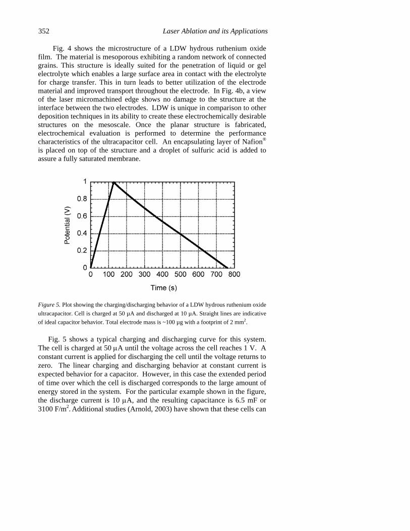
Fig. 4 shows the microstructure of a LDW hydrous ruthenium oxide film. The material is mesoporous exhibiting a random network of connected grains. This structure is ideally suited for the penetration of liquid or gel electrolyte which enables a large surface area in contact with the electrolyte for charge transfer. This in turn leads to better utilization of the electrode material and improved transport throughout the electrode. In Fig. 4b, a view of the laser micromachined edge shows no damage to the structure at the interface between the two electrodes. LDW is unique in comparison to other deposition techniques in its ability to create these electrochemically desirable structures on the mesoscale. Once the planar structure is fabricated, electrochemical evaluation is performed to determine the performance characteristics of the ultracapacitor cell. An encapsulating layer of Nafion® is placed on top of the structure and a droplet of sulfuric acid is added to assure a fully saturated membrane.
Figure 5. Plot showing the charging/discharging behavior of a LDW hydrous ruthenium oxide
ultracapacitor. Cell is charged at 50 µA and discharged at 10 µA. Straight lines are indicative
of ideal capacitor behavior. Total electrode mass is ~100 µg with a footprint of 2 mm2.
Fig. 5 shows a typical charging and discharging curve for this system.
The cell is charged at 50 A until the voltage across the cell reaches 1 V. A constant current is applied for discharging the cell until the voltage returns to zero. The linear charging and discharging behavior at constant current is expected behavior for a capacitor. However, in this case the extended period of time over which the cell is discharged corresponds to the large amount of energy stored in the system. For the particular example shown in the figure, the discharge current is 10 A, and the resulting capacitance is 6.5 mF or 3100 F/m2. Additional studies (Arnold, 2003) have shown that these cells can

14. Laser Forward Transfer of Electronic and Power Generating... 353 be discharged at currents above 50 mA and can be connected in series and parallel combinations to yield the proper additive values.
5.3 Advanced Laser Techniques for Micro-ultracapacitors: Self-filling Ultracapacitors
One of the key aspects of LDW for microultracapacitors is that the entire process is performed using a single tool. After LDW is used to deposit material, this material is baked prior to micromachining with the same laser. It is then necessary to add an encapsulant and excess electrolyte to perform the electrochemical tests. Although the main tool remains the same, these two processes require the ultracapacitor cell to be removed from the experimental apparatus costing additional time and effort. Furthermore, excess electrolyte makes packaging and handling more difficult.
By employing advanced laser techniques, the process can be dramatically simplified and optimized. Rather than bake the material prior to laser micromachining, it is possible to isolate the two electrodes without the need to remove electrolyte from the ink by employing two separate lasers. An IR laser can be used to drive electrolyte away from the location of interest. This is immediately followed by the UV laser for removing a stripe of electrode material (Arnold, 2004c).
The most interesting aspect of this dual laser approach is that after the two electrodes have been separated, the dividing groove refills with electrolyte. Although the fundamental mechanism for this is not well understood, the end result is a working ultracapacitor cell without excess electrolyte, and without the need to remove the substrate from the LDW apparatus.
LDW has been successfully used to fabricate small-scale ultracapacitor cells. Although the process has not been completely optimized, existing cells have been shown to have outstanding performance for energy and power density. Dual laser techniques enable a level of process optimization toward the ultimate goal of a commercialized product.
6. LASER DIRECT-WRITE OF MICROBATTERIES
The second type of electrochemical energy storage and power generation systems to be considered are batteries. In batteries, the stored chemical energy is converted to electrical energy through oxidation and reduction reactions at the electrodes. Electrons generated by oxidation of the anode material generate work in the electrical circuit before recombining to reduce

354 Laser Ablation and its Applications the cathode material. The separator/electrolyte enables the flow of ions between the anode and cathode to complete the circuit. The myriad of chemical possibilities are discussed and reviewed in readily available reference books (Vincent, 1997; Linden, 2001).
In the case of small-scale microbatteries, the main challenge is to create mesoscale patterns of these active materials while maintaining the necessary physical and chemical properties of a functioning cell. There has been significant effort to develop small microbatteries for various primary and secondary chemistries. Examples include secondary solid-state lithium-ion cells in a stacked configuration (Bates, 1995, 2000, Arnold 2004a) and primary alkaline microbatteries in a planar configuration where the anode and cathode are located adjacent to each other on the substrate (Humble, 2001; LaFollette, 2001; Arnold 2004c).
The next two sections describe the fabrication of single use (primary) and rechargeable (secondary) microbatteries using LDW processes. The primary microbatteries consist of zinc/silver-oxide alkaline cells. The secondary microbatteries are comprised of lithium and lithium-ion cells. Both types of microbatteries exhibit the appropriate open-circuit voltages characteristic of their chemistries. The primary cells are able to operate at relatively high discharge currents, while the secondary cells maintain high efficiencies and show limited charge fading through numerous charge/discharge cycles.
6.1 LDW of Primary Microbatteries
Alkaline batteries are one of the most ubiquitous battery chemistries in use today. Their low cost, relative environmental safety, and ability to handle high discharge rate applications make them readily available for consumer applications. In comparison to other alkaline chemistries, the zinc/silver-oxide (Zn-Ag2O) system has found extensive use in applications which require maintaining a constant voltage throughout the battery discharge. Primary Zn-Ag2O alkaline microbatteries have been demonstrated using LDW techniques by laser printing zinc and monovalent silver oxide (Ag2O) powders in both planar and stacked geometries on a variety of substrates (Arnold 2004a, 2004c; Pique 2004b), as shown in Fig. 6.
The planar alkaline microbattery cells are constructed by first preparing the substrates so that two electrically isolated current collector pads are obtained. The cathode ink (consisting of Ag2O powders plus 5 wt% graphite to improve conductivity, and a polymer binder mixed with an organic solvent) is first deposited followed by baking at 150 C for 5-10 minutes to remove the solvent and to bind the cathode to the substrate. Then the Zn ink (formed by mixing zinc powders and a polymer binder with an organic solvent) is deposited to form the anode and subsequently baked at 150 C for

14. Laser Forward Transfer of Electronic and Power Generating... 355 5-10 minutes. After deposition and processing of the cathode and anode, the separation gap between them is UV laser micromachined to remove any additional material that could cause shorting of the electrodes. The typical weight of all transferred material is 250 g, while the thickness of the anode and cathode layers is about 10-20 m thick. In order to activate the planar cells, a drop of 25 wt.% KOH solution is placed on the electrodes.
Figure 6. Optical micrographs showing (a) planar and (b) stacked alkaline microbatteries made by LDW. In (b), each of the layers required for the stacked structure are shown after being laser printed.
The fabrication of stacked alkaline microbatteries using LDW is
performed in similar fashion in terms of the electrode materials and processing. However, in this case, a separator layer, consisting of barium titanante 30 nm dia. nanoparticles and a cellulose binder, is laser printed on top of the cathode. Alternatively, a commercially available separator
2.5 mm
(a)
1 mm
(b)

356 Laser Ablation and its Applications material can be laser micromachined to the desired shape and size and manually placed on top of the cathode. To complete the stack, the Zn ink is laser printed on top of the separator. To avoid shorting between the cathode and anode layers, the separator layer is made larger in area than either of the electrode layers.
Electrochemical evaluation of cell voltage and discharge behavior of the alkaline microbatteries demonstrated similar behavior to that of larger cells (see Fig. 7). The open-circuit potential for both planar and stacked microbatteries was 1.55 V, while their discharge at constant currents showed the characteristic flat response of the Zn-Ag2O alkaline system. High capacity cells are obtained in this manner. For instance, planar cells have been fabricated with capacities greater than 450 Ahr/cm2. The relatively high discharge rate behavior is demonstrated in the stacked geometries by applying 1 mA for more than 12 minutes of discharge, corresponding to a power density of 1.9 mW/cm2.
Figure 7. Discharge plot from a planar alkaline microbattery at currents of 10 and 20 µAmps.
An important challenge remains in how to package these cells for
commercial use. Since a liquid consisting of a highly corrosive alkaline solution is used as the electrolyte of the Zn-Ag2O microbatteries, sealing of these tiny structures is not easily achieved without compromising their size and wasting significant mass and footprint on the packaging. A better alternative would be to fabricate “dry” microbatteries, where issues such as leakage and contamination of the electrolyte are not as critical, or employ embedding strategies as discussed later in the chapter.

14. Laser Forward Transfer of Electronic and Power Generating... 357 6.2 LDW of Secondary Microbatteries
Lithium microbatteries represent a relatively new battery chemistry that offers significantly higher energy densities than other rechargeable battery systems owing to the small size of Li and its high reduction potential. Secondary lithium ion intercalation microbatteries have been fabricated by laser printing LiCoO2 powders for the cathode and graphite powders for the anode in stacked geometries.
Two types of separators have been used to make the lithium cells. In one case, porous polymer membranes were laser cut and placed between the cathode and anode layers (Wartena, 2004), while on the other an ionically conductive polymer nanocomposite membrane was laser printed on top of the cathode layer (Sutto, 2006).
The LiCoO2 cathodes and carbon anodes were deposited by LDW onto aluminum and copper foils (15 mm x 15 mm x 40 m thick), respectively. Both the cathode and anode inks were prepared by mixing the powders with a polymer binder, poly(vinylidene fluoride-hexafluoropropylene) (PVDF-HFP), and an organic solvent, (dibasic ester). In this particular case, the area of the transferred electrodes is 10 mm x 10 mm. Transferred films are dried in a vacuum oven at 120 C for 2 days prior to placing them inside a dry glove box (oxygen less than 1 ppm), where they are assembled into cells using one of the two types of separator membranes. An optical micrograph of one of these solid-state Li-ion microbatteries is shown in Fig. 8(a).
Fig. 8 (b) shows the charge/discharge cycling performance (C/18 rate) of a packaged Li-ion microbattery, demonstrating the expected behavior for the LiCoO2/Li system. This microbattery had a charge/discharge efficiency of ~98% and a capacity per unit area of 205 µAhr/cm2, which compares favorably to the value of 163 µAhr/cm2 achieved for sputter deposited Li microbatteries reported by Bates, et al. (Bates, 2000).
6.3 Advanced Laser Techniques for Microbatteries: Developing Embedded Micropower Sources
One of the important issues for microbatteries and other small-scale electrochemical systems is the development of an appropriate packaging scheme that protects the device from environmental degradation and preserves the small size. In order to address this issue, one can utilize more advanced surface restructuring and processing that is possible with the LDW process.

358 Laser Ablation and its Applications
Figure 8. (a) Optical micrograph of a packaged Li-ion microbattery made by LDW. (b) Charge/discharge profile from one of these microbatteries (C/18 rate, cycles 3-5).
In many cases where microbatteries are required, one desires to place the cell directly on the substrate of the microdevice to be powered. In these cases, one can take advantage of the existing substrate as a packaging material by placing the battery within the substrate rather than on top of the substrate. For instance, in the case of fiberglass or polyimide circuit boards, one can laser micromachine pockets of desired dimensions and deposit each of the electrode layers inside as shown in Fig. 9(a). The problem is then reduced to sealing the top of the battery with a metallic current collector to produce a fully embedded solution. With further refinements, one can create a separator layer from the substrate itself by laser micromachining both top and bottom to leave a thin layer of polymer or fiberglass before refilling it from both sides. This is illustrated schematically in Fig. 9(b). In the case of solid-state Li-ion microbatteries, it is also possible to LDW all the layers inside a well within the substrate as shown in Fig. 9(c). The ability to
(a)

14. Laser Forward Transfer of Electronic and Power Generating... 359 completely transfer and assemble electrochemically and thermally stable micropower sources into bulk materials can be extended to more advanced applications in which the power source is directly incorporated and sealed within the substrates used by the microdevice (Arnold, 2004c).
Figure 9. (a) Optical micrograph showing the planar view of an embedded alkaline microbattery made by LDW. (b) Schematic showing an embedded stacked Li-ion microbattery in cross section view. (c) Optical micrograph of a solid-state Li-ion microbattery embedded in a polyimide substrate by LDW.
In summary, LDW processing is an enabling technology for the fabrication of primary and rechargeable microbatteries as the prior work demonstrates. Notably, the LDW is not chemistry specific, allowing different types of materials to be deposited using the same tool by simply changing the source ribbon. More advanced techniques such as deposition of a liquid phase polymer nanocomposite that dries into a solid, ionically conductive micron thick solid separator, or laser surface modifications for

360 Laser Ablation and its Applications embedded designs makes possible other types of microelectrochemical cells that can be incorporated into a wide variety of microdevices.
7. LASER DIRECT-WRITE OF DYE-SENSITIZED SOLAR CELLS
The dye-sensitized solar cell (DSSC) is a photosensitive electrochemical cell with a more complicated electrode configuration in comparison to the previous two systems. The anode in this case comprises of light-absorbing dye molecules attached to the surface of nanocrystalline-TiO2 (nc-TiO2) particles. The electrons generated by oxidation of the dye molecules are injected into the conduction band of the wide band-gap TiO2 and transported to the external circuit through a transparent conducting oxide layer. On the cathode side, a metal catalyst enables the direct reduction of the electrolyte itself (I-/I3
-), which subsequently reduces the oxidized dye molecules to their initial state. The schematic structure of a dye-sensitized solar cell is shown in Fig. 10.
Figure 10. Schematic showing the basic structure and operation of a typical dye-sensitized solar cell.

14. Laser Forward Transfer of Electronic and Power Generating... 361
Over the last decade, DSSCs based on nc-TiO2 films have been extensively studied as possible alternatives to silicon-based solar cells due to their high power conversion efficiencies (~ 10%) and expected low materials and manufacturing costs (O’Regan, 1991; Nazeeruddin, 1993; Barbe, 1997; Nakada, 2002). Mesoporous nc-TiO2 layers with high surface area are essential for achieving high efficiency in the DSSC system because a large amount of dye can be adsorbed on the surface of the nc-TiO2 particles resulting in an increased solar light absorption and an increased reacting interface per unit area. As described in earlier sections, the LDW process is ideally suited for generating these microstructures with arbitrary patterns on a variety of substrates. In this section, we will describe the use of LDW techniques for the fabrication of mesoporous nc-TiO2 electrodes for dye-sensitized solar cells (the remaining components are fabricated using traditional techniques). In addition, advanced laser processing techniques for in situ annealing and sintering of the films without damaging the underlying substrates are discussed with implications for active nc-TiO2 layers fabricated on flexible plastic substrates.
7.1 LDW of the nc-TiO2 Layer
The general structure of a LDW dye-sensitized solar cell is similar to the stacked geometry described in the previous section on microbatteries. However, in this case, we use traditional vapor deposition to create the transparent conducting oxide layers and Pt cathode. The inks used are made from water based colloidal suspensions of nc-TiO2 powders mixed with organic additives. Mesoporous, nc-TiO2 films are deposited onto fluorine-doped tin oxide (FTO)-coated glass substrates by LDW of these inks (Kim, 2004, 2005). The transferred films are dried in air and sintered in the oven at 450C for 30 minutes. Once the films are sintered, the electrode is soaked in the dye solution in order to coat the TiO2 surface. Finally, the completed cells are assembled and sealed using a Surlyn gasket to separate the anode and cathode layer and provide a reservoir for the I-/I3
- electrolyte. The thickness and mass of the nc-TiO2 layers can be easily controlled by
varying the number of LDW passes over the substrate. By looking at the cross-sectional SEM of Fig. 11(a), it is clear that no interfacial gaps are formed between the nc-TiO2 layers because the transferred material remains in the form of a viscous fluid after the LDW transfer. As with the previous cases, the transferred materials maintain a homogeneously distributed network of particles with a high degree of porosity, consistent with a high surface area structure. The 3-dimensional network of interconnected TiO2 nanoparticles enables good electron conduction while the high surface area structure can maximize the amount of dye adsorbed on the surface of the

362 Laser Ablation and its Applications TiO2 particles. Both properties are essential for the fabrication of efficient dye-sensitized solar cells.
Figure 11. SEM micrographs showing (a) the cross section and (b) the surface of a 12-µm thick nc-TiO2 layer transferred by LDW on FTO coated glass. The film was sintered at 450 °C for 30 min.
Fig. 12 shows the current density (J) versus voltage (V) characteristics for several dye sensitized solar cells containing LDW nc-TiO2 layers of varying thickness. The initial increase in Jsc with the nc-TiO2 film thickness can be related to the increased surface area of the TiO2 films and concomitantly the increased amount of adsorbed dye molecules. Although the thicker films allow for more adsorbed dye molecules and would be expected to produce higher photocurrents, in practice it is found that the very thick nc-TiO2 films also contain a large number of defect/recombination sites resulting in an overall decrease in the cell operational characteristics. Because of this, the thickness of the nc-TiO2 films must be optimized for improving both Jsc and Voc parameters simultaneously. In the current work, cells made with an optimum thickness of 15 m exhibited a Jsc of 10.1 mA/cm2, Voc of 0.64 V, a fill factor (ff) of 0.65, and a light power conversion efficiency () of ~ 4.3 %. The conversion efficiency is comparable to those reported earlier for analogous cells fabricated with commercial TiO2 powders (P25) using traditional techniques (Okuya, 2002; Nakada, 2002; Hinsch, 2001).
Glass
FTO
nc-TiO2
3m
(a)
(b) 200 nm

14. Laser Forward Transfer of Electronic and Power Generating... 363
Figure 12. Current density versus voltage (J-V) characteristics of dye-sensitized solar cells fabricated by laser based techniques with different thicknesses of active TiO2 layers under the light intensity of 100 mW/cm2 (AM 1.5 simulated solar illumination). The active cell area of all samples was 0.25 cm2.
7.2 Advanced Laser Techniques for DSSCs: in situ Laser Sintering of the nc-TiO2 Layer
To date, the use of organic additives, typically a poly(ethylene glycol)-based surfactant, is necessary for the formation of a viscous colloidal suspension that is essential in building crack-free thick films with increased porosity after sintering when using LDW or traditional fabrication approaches. In order to maximize the device efficiency, the bladed or printed nc-TiO2 electrodes must be sintered at relatively high temperatures (~ 450C) to remove the organic additives and to form an electrically connected nanostructure network within the mesoporous electrode. Due to the high sintering temperature required, most of the research and development (R&D) work on DSSCs has been limited to substrates that can withstand high temperatures such as glass and stainless steel. Considering manufacturing cost, flexibility and safety issues, the use of plastic substrates can offer many advantages over glass substrates because the DSSC devices based on plastic substrates would be cheaper, lighter, and thinner than the DSSC devices on glass substrates. For this reason, the traditional high temperature sintering should be replaced by a low temperature sintering process in the fabrication steps of nc-TiO2 electrodes.

364 Laser Ablation and its Applications
Using additional laser techniques within the LDW apparatus, it is possible to remove the high temperature sintering step from the overall process (Kim, 2005). Deposited films are first heat treated at 100 °C to remove excess solvent from the paste. This low temperature is not sufficient to remove organic additives from the deposited film (see Fig. 13(a)), but it is sufficient to form clusters approximately 100 - 200 nm in diameter due to the drying of the organic material. Such agglomerates are not well suited to form the electronically connected nanostructured network required for the proper operation of DSSCs. Typical laser sintering at IR wavelengths is insufficient for TiO2 due to its large band gap (3.0-3.2 eV) and low absorption in the IR region.
Figure 13. Cross sectional SEM micrographs of nc-TiO2 electrodes prepared on FTO-coated glass substrates. Both samples were first dried in an oven at 100 C for 18 hrs. Image (a) was taken before laser sintering, while (b) was obtained after laser sintering at 1 mm/min.

14. Laser Forward Transfer of Electronic and Power Generating... 365
However, by utilizing the same UV source (355 nm) that is used for the transfer of the nc-TiO2 inks, this problem can be surmounted resulting in sintered structures. Fig.13(b) shows that the laser sintering process is capable of removing the organic additives from the film and form an electrically connected network structure in the nc-TiO2 film.
To date, the power conversion efficiency of the devices based on the laser sintered nc-TiO2 electrodes is a factor of two greater than non-sintered films, but still less than what can be obtained from high temperature processes. However, these preliminary results indicate that the laser sintering technique is a promising approach for the fabrication of nc-TiO2 electrodes especially for plastic DSSCs.
The merit of this approach is that it allows both to transfer the TiO2 colloidal suspensions and in situ sinter the mesoporous nc-TiO2 electrodes using the same UV laser, thus simplifying the processing steps required for fabricating DSSCs at low temperatures. Further optimization of the laser sintering conditions such as power intensity, laser beam spot size and translation speed leave ample room for refinement of this technique.
8. THE FUTURE OF LASER DIRECT-WRITE
The use of LDW techniques for the transfer and processing of electronic and power generating materials has been reviewed in the previous sections. Numerous examples of the types of components fabricated using this technique are described and it is clear that the LDW process is well suited to transfer or print inks or fluids containing suspensions or mixtures of the required electronic materials. The cured inks result in conformal patterns that are continuous and well adhered to the substrate. Moreover, by choosing the appropriate powder materials and ink compositions, the same technique can also be used to generate patterns of mesoporous structures with extremely high effective surface areas required for fabricating components for hybrid micropower systems including ultracapacitors, microbatteries and dye-sensitized solar cells. Each of these are indispensable elements in the fabrication of autonomous, self-powered microelectronic systems such as wireless sensor networks. However, in order to reach the full potential of the LDW process it is desired that these elements be integrated into fully functional circuits.
Work toward this goal is progressing rapidly. Laser forward transfer and laser direct-write techniques are poised to play an important role in the development of the next generation of electronic systems as work toward the goal of complete device integration steadily progresses. For example, future microelectronic designs will require integration of many different and

366 Laser Ablation and its Applications increasingly smaller components. To achieve this, it is necessary to accurately place small-scale energy storage systems and individual electrical components such as semiconductor bare die and submillimeter discrete passive components on surfaces that may not be compatible with traditional “pick-and-place” equipment. The placement of each of these components onto virtually any type of surface is enabled by the use of laser transfer methods.
An alternative approach to device integration and miniaturization can be accomplished by incorporating electronic components, energy storage, and their interconnects within the volume of a substrate. Rather than limiting their placement to its surface, it will be possible to integrate electronic circuits within any type of form factor. The development of such “embedded” electronics is being explored using laser direct-write techniques. The remaining sections of this chapter will provide a brief overview of the latest developments taking place in device integration and embedding strategies.
8.1 Laser Transfer of Electronic Components
The use of LIFT processes for the transfer and placement of prefabricated parts or components onto a receiving substrate was first reported by Holmes et al. (Holmes, 1998). In their work, the authors describe the laser-driven release of Si-based microstructures from a UV-transparent substrate with an intermediate polymer sacrificial layer. Upon irradiation with an excimer laser pulse, a thin fraction of the sacrificial layer is vaporized, releasing the microstructure. This technique was later used to demonstrate the laser-assisted assembly of microelectromechanical devices from parts fabricated on separate substrates (Holmes, 2002). These initial results showed how to use LDW process as an alternative to conventional “pick-and-place” approaches for the placement of electronic components such as passives and semiconductor bare dies. The basic concept is quite simple: use a “sacrificial layer” such as the polymer layer used by Holmes to attach the individual components to a UV-transparent support. A laser pulse ablates the sacrificial layer generating gases that release and propel the component towards a receiving substrate placed in close proximity. This laser device transfer process is a contact-less process and thus allows the transfer of very small and very thin components, which could easily be damaged by “pick-and-place” tools.
Recently, this concept has been applied to the laser transfer of semiconductor bare dies. Karlitskaya and coworkers have developed a simple model that predicts the fluence threshold for the release of 200 x 200 µm2 by 150 µm thick Si dies held with a PVC sacrificial layer (Karlitskaya,

14. Laser Forward Transfer of Electronic and Power Generating... 367 2004). The model shows that the release threshold is below the damage threshold for the reverse side of the die (< 673 K) based on heat diffusion of the absorbed laser pulse through the Si substrate. In this case the authors assumed the laser transfer of devices with the active region facing opposite to the laser pulse. This configuration is not very practical since in order to establish the electrical connections between the pads on the transferred die and the acceptor substrate, extremely precise alignment is required. A better solution is to transfer the die with its active surface facing up enabling direct-write approaches to make contact to the device. The challenge however, is to be able to illuminate the active region of the die with the transfer laser pulse without damaging it. We have recently demonstrated this capability with the laser forward transfer of individual InGaN LED bare dies (250 x 350 µm2) using a series of very low fluence UV laser pulses (Piqué, 2005b). Once laser transferred, the LED’s are electrically tested and their operation verified. The fact that the devices are not damaged upon laser illumination of their active surface demonstrates the possibility to develop a uniquely versatile laser-based component placement and interconnecting system.
8.2 LDW of Embedded Electronic Circuits
The development of embedded surface mount devices (SMD’s), semiconductor bare die integrated circuits (IC’s), interconnects and power source elements, offers the ability to achieve levels of miniaturization beyond the capabilities of current manufacturing techniques. Given an arbitrary circuit design, significant reductions in volume and overall weight can be achieved by using embedded components. Furthermore, embedded circuits exhibit higher device density and improved electrical performance, resulting in enhanced functionality within a given form factor.
At the Naval Research Laboratory, we demonstrated the use of LDW techniques for the fabrication of embedded microbatteries and electronic circuits (Piqué, 2004a, 2005a). In this work, a simple blinker circuit comprised of six passive SMD components (4 resistors and 2 capacitors), two SMD LED’s and one unpackaged IC (LM555 chipset in bare die form) was embedded in a thermoplastic polyetherimide substrate using LDW.
Laser micromachining was used to generate the pockets in the substrate wherein each component was buried. Once in place, the components were buried under a layer of polyimide. The interconnects required by the circuit were made by laser micromachining vias to expose the contact pads on each device.

368 Laser Ablation and its Applications
Figure 14. (a) Circuit diagram for an embedded blinker circuit. (b) Optical micrograph of the embedded circuit made by LDW, with the bottom image showing the embedded circuit next to a packaged LM555 chip for size comparison.
The metal interconnects were then generated by laser printing a conductive silver ink. The resulting embedded circuit occupied a footprint smaller than a single packaged LM555 chip. Fig. 14 shows a schematic of the circuit and photographs of the embedded blinker circuit. It is estimated that these LDW embedded circuits will occupy footprints of about 1/4 or less and require less than 1/10 of the thickness of a printed circuit board design. This shows that by using LDW processes it is possible to fabricate functional electronic circuits buried within almost any surface, with the surface or substrate serving both as circuit board and packaging.

14. Laser Forward Transfer of Electronic and Power Generating... 369 9. SUMMARY AND OUTLOOK
Laser direct-write techniques encompass many laser-based processes, which allow the subtraction (i.e. laser micromachining), addition (i.e. laser transfer) and modification (i.e. laser annealing) of many types of materials. As this chapter has shown, LDW can be used for the generation of mesoscale patterns of electronic and power generating materials directly on a substrate without requiring lithographic processing. These patterns can be assembled to form simple structures such as metal lines for establishing the connections between devices in functional circuits, or more complex ones such as the multilayers required for a stacked Li-ion microbattery. The energy storage devices fabricated through this technique exhibit outstanding performance characteristics. In each case, the ability to transfer complex inks from a ribbon to an acceptor substrate under ambient conditions and without changing their physical or chemical properties is one of the unique attributes of the LDW process. Another key attribute of LDW processes is that they can be used for rapid prototyping applications, allowing the design, fabrication and testing of a given structure to be completed quickly.
The recent application of LDW techniques for the transfer of preformed devices such as semiconductor bare dies, and for embedding microbatteries and simple electronic circuits, opens the door for the development of a unique laser-based microelectronics fabrication tool. Such a tool would be capable of fabricating and embedding electronic circuits with the required power storage and power harvesting components within the same substrate. The resulting fully integrated systems could easily be reconfigured to fit within a desired form factor, thus allowing the placement of electronic systems in places that seem inconceivable today. In fact, the functionality of these LDW circuits can be customized for a particular application by choosing the appropriate electronic modules or building blocks from a circuit library available in the LDW tool. Such a LDW system does not yet exist, but it is just a matter of time before the various processes described in this chapter are combined into a single machine capable of making this vision a reality.
10. REFERENCES
Adrian, F.J., Bohandy, J., Kim, B.F., Jette, A.N., and Thompson, P., 1987, A study of the mechanism of metal deposition by the laser-induced forward transfer process, J. Vac. Sci. Technol. B5: 1490-1494.
Arnold, C. B., Wartena, R. C., Pratap, B., Swider-Lyons, K. E., and Piqué, A., 2002, Laser direct writing of hydrous ruthenium dioxide micro-pseudocapacitors, in: Electroactive

370 Laser Ablation and its Applications
Polymers and Rapid Prototyping, D. B. Chrisey and S. C. Danforth, ed., volume 689, pages 275–280, Pittsburgh, PA. Materials Research Society.
Arnold, C. B., Wartena, R. C., Swider-Lyons, K. E., and Piqué, A., 2003 . Direct-write planar micro-ultracapacitors by laser engineering, J. Electrochem. Soc. 150:A571–A575.
Arnold, C. B., Kim, H., Sutto, T.E., and Piqué, A., 2004a, Direct write laser processing for miniature electrochemical systems, Laser Focus World, 40: 9-12.
Arnold, C. B., Kim, H. and Piqué, A., 2004b, Laser transferred primary alkaline microbatteries, Appl. Phys. A, 79: 417-420.
Arnold, C.B., and Piqué, A., 2004c, Self-filling wet electrochemical cells by laser processing, US patent application 20040256359.
Arnold, C.B., Piqué, A., Auyeung, R. C. Y. and Nurnberger, M., 2004d, Laser-based technique for producing and embedding electrochemical cells and electronic components directly into circuit board materials, US patent application 2005000613.
Auyeung, R.C.Y., Wu, H.D., Modi, R., Piqué, A., Fitz-Gerald, J.M., Young, H.D., Lakeou, S., Chung, R., and Chrisey, D.B., 2000, Matrix-assisted laser transfer of electronic materials for direct-write applications, Proc. SPIE 4088: 393-396.
Bähnisch, R., Gross, W., and Menschig, A., 2004, Single-shot, high repetition rate metallic pattern transfer, Microelectronic Engineering 50: 541-546.
Barbe, C. J., Arendse, F., Comte, P., Jirousek, M., Lenzmann, F., Shklover, V., and Grätzel, M., 1997, Nanocrystalline titanium oxide electrodes for photovoltaic applications, J. Am. Ceram. Soc. 80: 3157-3171.
Bates, J.D., Dudney, N. J., Lubben, D. C., Gruzalski, G. R., Kwak, b. S., Yu, X., and Zuhr, R. A., 1995, Thin-film rechargeable lithium batteries, J. Power Sources 54: 58-62.
Bates, J. B., Dudney, N. J., Neudecker, B., Ueda, A., and Evans, C. D., 2000, Thin-film lithium and lithium-ion batteries, Solid State Ionics 135: 33-45.
Bohandy, J., Kim, B.F., Adrian, F.J., 1986, Metal deposition from a supported metal film using an excimer laser, J. of Appl. Phys. 60: 1538-1539.
Bohandy, J., Kim, B.F., Adrian, F.J., and Jette, A.N., 1988, Metal deposition at 532 nm using a laser transfer technique, J. Appl. Phys. 63: 1158-1162.
Conway, B. E. 1999, Electrochemical Supercapacitors, Scientific Fundamentals and Technological Applications, Kluwer Academic, New York.
Dmowski, W., Egami, T., Swider-Lyons, K. E., Love, C. T., and Rolison, D. R., 2002, Local atomic structure and conduction mechanism of nanocrystalline hydrous RuO2 from x-ray scattering, J. Phys. Chem. B 106:12677–12683.
Esrom, H., Jun-Ying Zhang, Kogelschatz, U., and Pedraza, A.J., 1995, New approach of a laser-induced forward transfer for deposition of patterned thin metal films, Appl. Surf. Sci. 86: 202-207.
Fang, Q. L., Evans, D. A., Roberson, S. L., and Zheng, J. P., 2001, Ruthenium oxide film electrodes prepared at low temperatures for electrochemical capacitors, J. Electrochem. Soc. 148:A833–A837.
Fernandez-Pradas, J.M., Colina, M., Serra, P., Dominguez, J., and Morenza, J.L., 2004, Laser-induced forward transfer of biomolecules, Thin Sol. Films 453-454: 27-30.
Fogarassy, E., Fuchs, C., Kerherve, F., Hauchecorne, G., and Perriere, J., 1989, Laser-induced forward transfer of high-Tc YBaCuO and BiSrCaCuO superconducting thin films, J. Appl. Phys. 66: 457-459.
Greer, J. A. and Parker, T. E., 1988, Laser-induced forward transfer of metal oxides to trim the frequency of surface acoustic wave resonator devices, Proc. SPIE 998: 113-125.
Herman, I. P., 1989, Laser-assisted deposition of thin films from gas-phase and surface-adsorbed molecules, Chem. Rev. 89:1323-1357.
14. Laser Forward Transfer of Electronic and Power Generating... 371 Hinsch, A., Kroon, J. M., Kern, R., Uhlendorf, I., Holzbock, J., Meyer, A., and Ferber, 2001,
Long-term stability of dye-sensitized solar cells, J., Prog. Photovolt: Res. Appl. 9: 425-438.
Holmes, A.S., and Saidam, S.M., 1998, Sacrificial layer process with laser-driven release for batch assembly operations, J. of Microelectromechanical Sys., 7:416-422.
Holmes, A.S., 2002, Laser processes for MEMS manufacture, Proc. SPIE 4426:203-209. Humble, P. H., Harb, J. N., and LaFollettte, R., 2001, Microscopic nickel-zinc batteries for
use in autonomous microsystems, J. Electrochem. Soc. 18: A1357-A1361. Ito, S., Takeuchi, T., Katayama, T., Sugiyama, M., Matsuda, M., Kitamura, T., Wada, Y., and
Yanagida, S., 2003, Conductive and transparent multilayer films for low-temperature-sintered mesoporous TiO2 electrodes of dye-sensitized solar cells, Chem. Mater. 15: 2824-2828.
Kalyanasundaram, K., and Grätzel, M., 1998, Applications of functionalized transition metal complexes in photonic and optoelectronic devices, Coordination Chemical Reviews 77: 347-414.
Kántor, Z., Tóth, Z., Szorenyi, T., and Tóth, A.L., 1994, Deposition of micrometer-sized tungsten patterns by laser transfer technique, Appl. Phys. Lett. 64: 3506-3508.
Karaiskou, A., Zergioti, I., Fotakis, C., Kapsetaki, M., and Kafetzopoulos, D., 2003, Microfabrication of biomaterials by the sub-ps laser-induced forward transfer process, Appl. Surf. Sci. 208-209: 245-249.
Kim, H., Kushto, G. P., Arnold, C. B., Kafafi, Z. H., and Piqué, A., 2004, Laser processing of nanocrystalline TiO2 films for dye-sensitized solar cells, Appl. Phys. Lett. 85: 464-466.
Kim, H., Auyeung, R.C.Y., Ollinger, M., Kushto, Kafafi, Z. H., and Piqué, A., 2005, Laser-sintered mesoporous TiO2 electrodes for dye-sensitized solar cells, accepted for publication in Appl. Phys. A.
Kim, I. H. and Kim, K. B., 2001, Ruthenium oxide thin film electrodes for supercapacitors. Electrochem, Solid-State Lett. 5:A62–A64.
Koeneman, P. B., Busch-Vishniac, I. J., and Wood, K. L., 1997, Feasibility of micro power supplies for MEMS, J. Microelectromech. Sys. 6:355–362.
LaFollettte, R., Harb, J. N., and Humble, P., 2001, in: Sixteenth Annu. Battery Conf. Applications and Advances, R.S.L. Das and H. Frank, ed., IEEE, Piscatawy, NJ, pp. 349-354.
Linden, D. and Reddy, T. B., 2001, Handbook of Batteries, 3rd ed., McGraw-Hill, New York. McKeown, D. A., Hagans, P. L., Carette, L. P. L., Russell, A. E., Swider, K. E., and Rolison,
D. R., 1999, Structure of hydrous ruthenium oxides: Implications for charge storage, J. Phys. Chem. B 103:4825–4832.
Modi, R., Wu, H.D., Auyeung, R.C.Y., Gilmore, C.M., and Chrisey, D.B., 2001, Direct writing of polymer thick film resistors using a novel laser transfer technique, J. Mater. Res. 16:3214-3222.
Nakada, S., Matsuda, M., Kambe, S., Saito, Y., Kitamura, T., Sakata, T., Wada, Y., Mori, H., and Yanagida, S., 2002, Dependence of TiO2 nanoparticle preparation methods and annealing temperature on the efficiency of dye-sensitized solar cells, J. Phys. Chem. B 106: 10004-10010.
Nazeeruddin, M. K., Kay, A., Rodicio, I., Humphry-Baker, R., Muller, E., Liska, P., Vlachopoulos, N., and Grätzel, M., 1993, Conversion of light to electricity by cis-X2Bis(2,2’-bipyridyl-4,4’-dicarboxylate)ruthenium(II) charge-transfer sensitizers (X = Cl-, Br-, I-, CN-, and SCN-) on nanocrystalline TiO2 electrodes, J. Am. Chem. Soc. 115: 6382-6390.

372 Laser Ablation and its Applications Okuya, M., Nakade, K., and Kaneko, S., 2002, Porous TiO2 thin films synthesized by a spray
pyrolysis deposition (SPD) technique and their application to dye-sensitized solar cells, Sol. Energy Mater. Sol. Cells 70: 425-435.
O’Regan, B. and Grätzel, M., 1991, A low-cost, high-efficiency solar cell based on dye-sensitized colloidal TiO2 films, Nature 353: 737-740.
Osgood, R. M. and Deutsch, T. F., 1985, Laser-induced chemistry for microelectronics, Science 227: 709-714.
Papakonstantinou, P., Vainos, N.A., and Fotakis, C., 1999, Microfabrication by UV femtosecond laser ablation of Pt, Cr and indium oxide thin films, Appl. Surf. Sci. 151: 159-170.
Pimenov, S.M., Shafeev, G.A., Smolin, A.A., Konov, V.I., and Vodolaga, B.K., 1995, Laser-induced forward transfer of ultra-fine diamond particles for selective deposition of diamond films, Appl. Surf. Sci. 86: 208-212.
Piqué, A., Chrisey, D.B., Auyeung, R.C.Y., Lakeou, S., Chung, R., McGill, R.A., Wu, P.K., Duignan, M., Fitz-Gerald, J., and Wu, H.D., 1999a, Laser direct writing of circuit elements and sensors, Proc. SPIE 3618: 330-339.
Piqué, A., Chrisey, D.B., Auyeung, R.C.Y., Fitz-Gerald, J., Wu, H.D., McGill, R.A., Lakeou, S., Wu, P.K., Nguyen, V., and Duignan, M., 1999b, A novel laser transfer process for direct writing of electronic and sensor materials, Appl. Phys. A A69: 279-284.
Piqué, A., Chrisey, A.D.B., Fitz-Gerald, J.M., McGill, R.A., Auyeung, R.C.Y., Wu, H.D., Lakeou, S., Nguyen, V., Chung, R., and Duignan, M., 2000a, Direct writing of electronic and sensor materials using a laser transfer technique, J. Mater. Res. 15: 1872-1875.
Piqué, A., Fitz-Gerald, J., Chrisey, D.B., Auyeung, R.C.Y., Wu, H.D., Lakeou, S., and McGill, R.A., 2000b, Direct writing of electronic materials using a new laser assisted transfer/annealing technique, Proc. SPIE 3922: 105-112.
Piqué, A., Weir, D.W., Wu, P.K., Pratap, B., Arnold, C.B., Ringeisen, B.R., McGill, R.A., Auyeung, R.C.Y., Kant, R.A., and Chrisey, D.B., 2002, Direct-write of sensor devices by a laser forward transfer technique, Proc. SPIE 4637: 361-368.
Piqué, A., Arnold, C.B., Pratap, B., Auyeung, R.C.Y., Kim, H., and Weir, D.W., 2003, Laser direct-write of metal patterns for interconnects and antennas, Proc. SPIE 4977: 602-608.
Piqué, A., Mathews, S.A., Auyeung, R.C., Ollinger, M., Kim, H., Pratap, B., Arnold, C.B., and Sutto, T.E., 2004a, Application of laser direct-write techniques for embedding electronic and micropower components, Proc. SPIE 5662: 564-569.
Piqué, A., Arnold, C. B., Kim, H., Ollinger, M., and Sutto, T.E., 2004b, Rapid prototyping of micro-power sources by laser direct-write, Appl. Phys. A, 79: 783-786.
Piqué, A., Pratap, B., Mathews, S. A., Karns, B. J., Auyeung, R. C., Kasser, M., Ollinger, M., Kim, H., Lakeou, S., and Arnold, C.B., 2005a, Laser direct-write of embedded electronic components and circuits, Proc. SPIE 5713: 223-230.
Piqué, A., Mathews, S. A., Pratap, B., and Auyeung, R. C., 2005b, Laser forward transfer of semiconductor devices, Laser Precision Microfabrication Conference, Williamsburg VA.
Sarangapani, S., Tilak, B., and Chen, C., 1996, Materials for electrochemical capacitors. J. Electrochem. Soc. 143:3791–3799.
Schultze, V., and Wagner, M, 1991, Laser-induced forward transfer of aluminum, Appl. Surf. Sci. 52:303-309.
Serra, P., Colina, M., Fernandez-Pradas, J.M., Sevilla, L., and Morenza, J.L., 2004, Preparation of functional DNA microarrays through laser-induced forward transfer, Appl. Phys. Lett. 85: 1639-1641.
Sutto, T. E., Ollinger, M., Kim, H., Arnold, C.B. and Piqué, A., 2006, Laser transferable polymer-ionic liquid separator/electrolytes for solid-state rechargeable lithium ion microbatteries, Electrochem. Solid-State Lett. 9:A69-A71.

14. Laser Forward Transfer of Electronic and Power Generating... 373 Tolbert, W.A., Lee, I.-Y.S., Doxtader, M.M., Ellis, E.W., and Dlott, D.D., 1993a, High-speed
color imaging by laser ablation transfer with a dynamic release layer: fundamental mechanisms, J. Imaging. Sci. Tech. 37: 411-421.
Tolbert, W.A., I-Yin Sandy Lee, Xiaoning Wen, Dlott, D.D., Doxtader, M.M., and Ellis, E.W., 1993b, Laser ablation transfer imaging using picosecond optical pulses: ultra-high speed, lower threshold and high resolution, J. Imaging. Sci. Tech. 37: 485-489.
Tóth, Z., Szorenyi, T., and Tóth, A.L., 1993, Ar+ laser-induced forward transfer (LIFT): a novel method for micrometer-size surface patterning, Appl. Surf. Sci. 69: 317-320.
Trasatti, S. and Kurzweil, P., 1994, Electrochemical supercapacitors as versatile energy stores, Plat. Met. Rev. 38:46–56.
Vincent, C. A. and Scrosati, B., 1997, Modern Batteries, 2nd ed., Arnold, London. Wartena, R. C., Curtright, A.E., Arnold, C. B., Piqué, A. and Swider-Lyons, K. E., 2004, Li-
ion microbatteries generated by laser direct write, J. Power Sources 126: 193-202. Wu, P.K., Ringeisen, B.R., Callahan, J., Brooks, M., Bubb, D.M., Wu, H.D., Piqué, A.,
Spargo, B., McGill, R.A., and Chrisey, D.B., 2001, The deposition, structure, pattern deposition, and activity of biomaterial thin-films by matrix-assisted pulsed-laser evaporation (MAPLE) and MAPLE direct write, Thin Sol. Films 389-399:607-614.
Young, D., Auyeung, R.C.Y., Piqué, A., Chrisey, D.B., and Dlott, D.D., 2001a, Time-resolved optical microscopy of a laser-based forward transfer process, Appl. Phys. Lett. 78:3169-3171.
Young, D., Wu, H.D., Auyeung, R.C.Y., Modi, R., Fitz-Gerald, J., Piqué, A., Chrisey, D.B., Atanassova, P., and Kodas, T., 2001b, Dielectric properties of oxide structures by a laser-based direct-writing method, J. Mater. Res. 16:1720-1725.
Young, D., Auyeung, R.C.Y., Piqué, A., Chrisey, D.B., and Dlott, D.D., 2002, Plume and jetting regimes in a laser based forward transfer process as observed by time-resolved optical microscopy, Appl. Surf. Sci. 197-198:181-187.
Zergioti, I., Mailis, S., Vainos, N.A., Papakonstantinou, P., Kalpouzos, C., Grigoropoulos, C.P., and Fotakis, C., 1998a, Microdeposition of metal and oxide structures using ultrashort laser pulses, Appl. Phys. A 66: 579-582.
Zergioti, I., Malilis, S., Vainos, N.A., Fotakis, C., Chen, S., and Grigoropoulos, C.P., 1998b, Microdeposition of metals by femtosecond excimer laser, Appl. Surf. Sci. 127-129: 601-605.
Zergioti, I., Karaiskou, A., Papazoglou, D.G., Fotakis, C., Kapsetaki, M., and Kafetzopoulos, D., 2005, Femtosecond laser microprinting of biomaterials, Appl. Phys. Lett. 86: 163902-1-163902-3.
Zhang, C., Liu, D., Mathews, S.A., Graves, J., Schaefer, T.M., Gilbert, B.K., Modi, R.,Wu, H.-D., and Chrisey, D.B., 2003, Laser direct-write and its application in low temperature Co-fired ceramic (LTCC) technology, Microelectronic Eng. 70:41-49.
Zheng, J. P., Cygan, P. J., and Jow, T. R., 1995, Hydrous ruthenium oxide as an electrode material for electrochemical capacitors, J. Electrochem. Soc. 142:2699–2703.
Zheng, J. P. and Xin, Y., 2002, Characterization of RuO2 · xH2O with various water contents, J. Power Sources 110:86–90.


![[EHNUR WP 6] NUCLEAR FUEL AND AVAILABILITY · 2015-12-07 · [EHNUR WP 6] NUCLEAR FUEL AND AVAILABILITY . WERNER ZITTEL. 1, NIKOLAUS ARNOLD2, WOLFGANG LIEBERT3. VIENNA/OTTOBRUNN/DAR](https://static.fdocuments.in/doc/165x107/5f561149df0144327534a571/ehnur-wp-6-nuclear-fuel-and-2015-12-07-ehnur-wp-6-nuclear-fuel-and-availability.jpg)


