CHAPTER 13 SEMICONDUCTOR LASERS -...
55
CHAPTER 13 SEMICONDUCTOR LASERS Pamela L. Derry Luis Figueroa Chi-Shain Hong Boeing Defense & Space Group Seattle , Washington 13.1 GLOSSARY A Constant approximating the slope of gain versus current or carrier density C Capacitance c Speed of light D Density of states for a transition D c Density of states for the conduction band D y Density of states for the valence band d Active layer thickness d ef f Ef fective beam width in the transverse direction d G Guide layer thickness dg / dN Dif ferential gain E Energy of a transition E c Total energy of an electron in the conduction band E g Bandgap energy E n The nth quantized energy level in a quantum well E c n The nth quantized energy level in the conduction band E y n The nth quantized energy level in the valence band E y Total energy of a hole in a valence band e Electronic charge F c Quasi-Fermi level in the conduction band F y Quasi-Fermi level in the valence band f c Fermi occupation function for the conduction band f d Damping frequency f o Resonant frequency of an LRC circuit f p Peak frequency 13.1
Transcript of CHAPTER 13 SEMICONDUCTOR LASERS -...
CHAPTER 13 SEMICONDUCTOR LASERS
Pamela L . Derry Luis Figueroa Chi-Shain Hong Boeing Defense & Space Group Seattle , Washington
1 3 . 1 GLOSSARY
A Constant approximating the slope of gain versus current or carrier density
C Capacitance
c Speed of light
D Density of states for a transition
D c Density of states for the conduction band
D y Density of states for the valence band
d Active layer thickness
d ef f Ef fective beam width in the transverse direction
d G Guide layer thickness
dg / dN Dif ferential gain
E Energy of a transition
E c Total energy of an electron in the conduction band
E g Bandgap energy
E n The n th quantized energy level in a quantum well
E c n The n th quantized energy level in the conduction band
E y n The n th quantized energy level in the valence band
E y Total energy of a hole in a valence band
e Electronic charge
F c Quasi-Fermi level in the conduction band
F y Quasi-Fermi level in the valence band
f c Fermi occupation function for the conduction band
f d Damping frequency
f o Resonant frequency of an LRC circuit
f p Peak frequency
13 .1

13 .2 OPTICAL SOURCES
f r Resonance frequency
f y Fermi occupation function for the valence band
g Model gain per unit length
g t h Threshold modal gain per unit length
H Heavyside function
h Refers to heavy holes
" Plank’s constant divided by 2 π I Current
I of f DC bias current before a modulation pulse
I o n Bias current during a modulation pulse
I t h Threshold current
J Current density
J o Transparency current density
J t h Threshold current density
K Constant dependent on the distribution of spectral output function
k Wavevector
k Boltzmann constant
L Inductance
L Laser cavity length
L c Coherence length
L z Quantum well thickness
l Refers to light holes
u M u 2 Matrix element for a transition
m Ef fective mass of a particle
m c Conduction band mass
m r Ef fective mass of a transition
m y Valence band mass
N Carrier density
N 0 Transparency carrier density
n ef f Ef fective index of refraction
n r Index of refraction
n s p Spontaneous emission factor
P Photon density
P of f Photon density before a modulation pulse
P o n Photon density during a modulation pulse
R Resistance
R F Front facet reflectivity
R R Rear facet reflectivity
T Temperature
SEMICONDUCTOR LASERS 13 .3
w Laser stripe width a Absorption coef ficient a Linewidth enhancement factor a i Internal loss per unit length b Spontaneous emission factor G Optical confinement factor
D f 1/2 Frequency spectral linewidth D l L Longitudinal mode spacing
D l 1/2 Half-width of the spectral emission in terms of wavelength l Wavelength
l o Wavelength of the stimulated emission peak τ d Turn-on time delay τ p Photon lifetime τ s Carrier lifetime
1 3 . 2 INTRODUCTION
This chapter is devoted to the performance characteristics of semiconductor lasers . In addition , some discussion is provided on fabrication and applications . In the first section we describe some of the applications being considered for semiconductor lasers . The following several sections describe the basic physics , fabrication , and operation of a variety of semiconductor laser types , including quantum well and strained layer lasers . Then we describe the operation of high-power laser diodes , including single element and arrays . A number of tables are presented which summarize the characteristics of a variety of lasers . Next we discuss the high-speed operation and provide the latest results , after which we summarize the important characteristics dealing with the spectral properties of semicon- ductor lasers . Finally , we discuss the properties of surface emitting lasers and summarize the latest results in this rapidly evolving field .
More than 260 references are provided for the interested reader who requires more information . In this Handbook , Chap . 12 (LEDs) also contains related information . For further in-depth reviews of semiconductor lasers we refer the reader to the several excellent books which have been written on the subject . 1–5
1 3 . 3 APPLICATIONS FOR SEMICONDUCTOR LASERS
The best-known application of diode lasers is in optical communication systems . However , there are many other potential applications . In particular , semiconductor lasers are being considered for high-speed optical recording , 6 high-speed printing , 7 single- and multimode database distribution systems , 8 long-distance transmission , 9 submarine cable transmission , 1 0
free-space communications , 1 1 local area networks , 1 2 Doppler optical radar , 1 3 optical signal processing , 1 4 high-speed optical microwave sources , 1 5 pump sources for other solid-state lasers , 1 6 fiber amplifiers , 1 7 and medical applications . 1 8
For very high speed optical recording systems ( . 100 MB / s) , laser diodes operating at relatively short wavelengths ( l , 0 . 75 m m) are required . In the past few years , much progress has been made in developing short-wavelength semiconductor lasers , although the output powers are not yet as high as those of more standard semiconductor lasers .
13 .4 OPTICAL SOURCES
One of the major applications for lasers with higher power and wide temperature of operation is in local area networks . Such networks will be widely used in high-speed computer networks , avionic systems , satellite networks , and high-definition TV . These systems have a large number of couplers , switches , and other lossy interfaces that determine the total system loss . In order to maximize the number of terminals , a higher-power laser diode will be required .
Wide temperature operation and high reliability are required for aerospace applications in flight control and avionics . One such application involves the use of fiber optics to directly link the flight control computer to the flight control surfaces , and is referred to as fly-by-light (FBL) . A second application involves the use of a fiber-optic data network for distributing sensor and video information .
Finally , with the advent of ef ficient high-power laser diodes , it has become practical to replace flash lamps for the pumping of solid-state lasers such as Nd : YAG . Such an approach has the advantages of compactness and high ef ficiency . In addition , the use of strained quantum well lasers operating at 0 . 98 m m has opened significant applications for high-gain fiber amplifiers for communications operating in the 1 . 55- m m wavelength region .
1 3 . 4 BASIC OPERATION
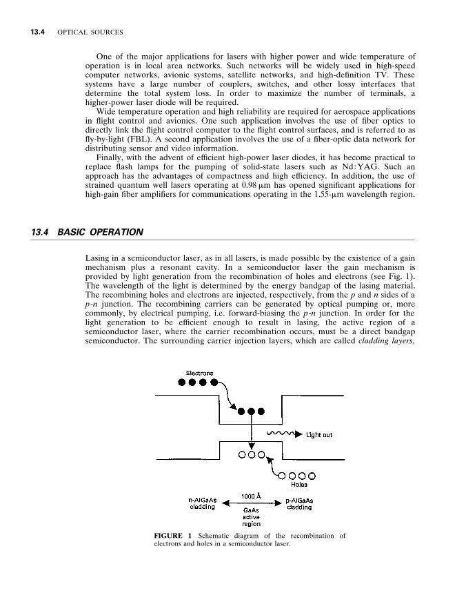
Lasing in a semiconductor laser , as in all lasers , is made possible by the existence of a gain mechanism plus a resonant cavity . In a semiconductor laser the gain mechanism is provided by light generation from the recombination of holes and electrons (see Fig . 1) . The wavelength of the light is determined by the energy bandgap of the lasing material . The recombining holes and electrons are injected , respectively , from the p and n sides of a p - n junction . The recombining carriers can be generated by optical pumping or , more commonly , by electrical pumping , i . e . forward-biasing the p - n junction . In order for the light generation to be ef ficient enough to result in lasing , the active region of a semiconductor laser , where the carrier recombination occurs , must be a direct bandgap semiconductor . The surrounding carrier injection layers , which are called cladding layers ,
FIGURE 1 Schematic diagram of the recombination of electrons and holes in a semiconductor laser .
SEMICONDUCTOR LASERS 13 .5
(a)
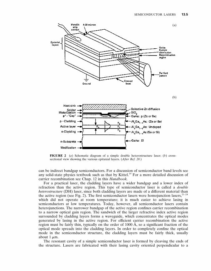
(b)
FIGURE 2 ( a ) Schematic diagram of a simple double heterostructure laser ; ( b ) cross- sectional view showing the various epitaxial layers . ( After Ref . 2 0 . )
can be indirect bandgap semiconductors . For a discussion of semiconductor band levels see any solid-state physics textbook such as that by Kittel . 1 9 For a more detailed discussion of carrier recombination see Chap . 12 in this Handbook .
For a practical laser , the cladding layers have a wider bandgap and a lower index of refraction than the active region . This type of semiconductor laser is called a double heterostructure (DH) laser , since both cladding layers are made of a dif ferent material than the active region (see Fig . 2) . The first semiconductor lasers were homojunction lasers , 21–24
which did not operate at room temperature ; it is much easier to achieve lasing in semiconductors at low temperatures . Today , however , all semiconductor lasers contain heterojunctions . The narrower bandgap of the active region confines carrier recombination to a narrow optical gain region . The sandwich of the larger refractive index active region surrounded by cladding layers forms a waveguide , which concentrates the optical modes generated by lasing in the active region . For ef ficient carrier recombination the active region must be fairly thin , typically on the order of 1000 Å , so a significant fraction of the optical mode spreads into the cladding layers . In order to completely confine the optical mode in the semiconductor structure , the cladding layers must be fairly thick , usually about 1 m m .
The resonant cavity of a simple semiconductor laser is formed by cleaving the ends of the structure . Lasers are fabricated with their lasing cavity oriented perpendicular to a
13 .6 OPTICAL SOURCES
natural cleavage plane . For typical semiconductor materials this results in mirror reflectivities of about 30 percent . If necessary , the reflectivities of the end facets can be modified by applying dielectric coatings to them . 2 5 For applications where it is not possible to cleave the laser facets , it is also possible to etch them , 26–28 although this is much more dif ficult and usually does not work as well . Laser cavity lengths can be anywhere from about 50 to 2000 m m , although commercially available lasers are typically 200 to 1000 m m long .
Unpumped semiconductor material absorbs light of energy greater than or equal to its bandgap . When the semiconductor material is pumped optically or electrically , it reaches a point at which it stops being absorbing . This point is called transparency . If it is pumped beyond this point it will have optical gain , which is the opposite of absorption . A semiconductor laser is subject to both internal and external losses . For lasing to begin , i . e ., to reach threshold , the gain must be equal to these optical losses . The threshold gain per unit length is given by :
g t h 5 a i 1 1
2 L ln S 1
R F R R D (1)
where a i is the internal loss per unit length , L is the laser cavity length , and R F and R R are the front and rear facet reflectivities . (For semiconductor lasers , gain is normally quoted as gain per unit length in cm 2 1 . This turns out to be very convenient , but unfortunately is confusing for people in other fields , who are used to gain being unitless . )
The internal loss is a material parameter determined by the quality of the semiconduc- tor layers . Mechanisms such as free-carrier absorption and scattering contribute to a i .
1 The second term in Eq . (1) is the end loss . A long laser cavity will have reduced end loss , since the laser light reaches the cavity ends less frequently . Similarly , high facet reflectivities also decrease the end loss , since less light leaves the laser through them .
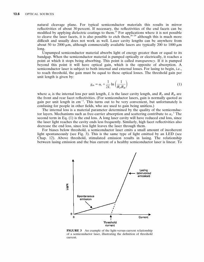
For biases below threshold , a semiconductor laser emits a small amount of incoherent light spontaneously (see Fig . 3) . This is the same type of light emitted by an LED (see Chap . 12) . Above threshold , stimulated emission results in lasing . The relationship between lasing emission and the bias current of a healthy semiconductor laser is linear . To
FIGURE 3 An example of the light-versus-current relationship of a semiconductor laser , illustrating the definition of threshold current .
SEMICONDUCTOR LASERS 13 .7
find the threshold current of a laser this line is extrapolated to the point at which the stimulated emission is zero (see Fig . 3) .
For further discussion of optical gain in semiconductors , see under ‘‘Quantum Well Lasers’’ later in this chapter . For more detail , see one of the books that has been written about semiconductor lasers . 1–5
1 3 . 5 FABRICATION AND CONFIGURATIONS
In order to fabricate a heterostructure laser , thin semiconductor layers of varying composition must be grown on a semiconductor substrate (normally GaAs or InP) . There are three primary epitaxial methods for growing these layers : liquid phase epitaxy (LPE) , molecular beam epitaxy (MBE) , and metalorganic chemical vapor deposition (MOCVD) , which is also called organometallic vapor phase deposition (OMVPE) .
Most of the laser diode structures which have been developed were first grown by LPE . 2 9 For a description of LPE see Chap . 12 . Most commerically available lasers are grown by LPE ; however , it is not well suited for growing thin structures such as quantum well lasers , because of lack of control and uniformity , especially over large substrates . 3 0
MBE and MOCVD are better suited for growths of thin , uniform structures . MOCVD 31 , 32 is basically a specialized form of chemical vapor deposition . In MOCVD ,
gases reacting over the surface of a substrate form epitaxial layers ; some of the gases are metalorganics . MOCVD is well suited for production environments , since epitaxial layers can be grown simultaneously on multiple large-area substrates and quickly , compared to MBE . It is expected that more commercial laser diodes will be grown by MOCVD in the future .
In the simplest terms , MBE 30 , 33 , 34 , 35 is a form of vacuum evaporation . In MBE growth occurs through the thermal reaction of thermal beams of atoms and molecules with the substrate , which is held at an appropriate temperature in an ultrahigh vacuum . MBE is dif ferent from simple vacuum evaporation for several reasons : the growth is single crystalline ; the growth is much more controlled ; and the vacuum system , evaporation materials , and substrate are cleaner .
With MOCVD the sources are gases , while with MBE they are solids . There are advantages and disadvantages to both types of sources . With gaseous sources the operator must work with arsine and / or phosphine , which are extremely hazardous gases . Solid- source phosphorus , however , is very flammable . Also , with MBE balancing the ratios of arsenic and phosphorus is extremely dif ficult ; therefore , MOCVD is the preferred method for growth of GaInAsP and InP . MBE is a slower growth process (on the order of 1 – 2 m m per hour) than MOCVD . MBE therefore has the control necessary to grow very thin structures (10 Å ) , but MOCVD is more ef ficient for production . MBE has a cleaner background environment , which tends to make it better suited for growths at which background impurities must be kept at a minimum . Newer growth techniques , 36 , 37 which combine some of the advantages of both MBE and MOCVD , are gas source MBE , metalorganic MBE (MOMBE) , and chemical beam epitaxy (CBE) . In these growth techniques the background environment is that of MBE , but some or all of the sources are gases , which makes them more practical for growth of phosphorus-based materials .
Double heterostructure (DH) semiconductor lasers can be fabricated from a variety of lattice-matched semiconductor materials . The two material systems most frequently used are GaAs / Al x Ga 1 2 x As and In 1 2 x Ga x As y P 1 2 y / InP . All of these semiconductors are III-V alloys . The GaAs / Al x Ga 1 2 x As material system has the advantage that all compositions of Al x Ga 1 2 x As are closely lattice-matched to GaAs , which is the substrate . For GaAs-based lasers , the active region is usually GaAs or low Al concentration Al x Ga 1 2 x As ( x , 0 . 15) , which results in lasing wavelengths of 0 . 78 – 0 . 87 m m . Al x Ga 1 2 x As quantum well lasers with wavelengths as low as 0 . 68 m m have been fabricated , 3 8 but the performance is reduced .
13 .8 OPTICAL SOURCES
In the In 1 2 x Ga x As y P 1 2 y / InP material system , the active region is In 1 2 x Ga x As y P 1 2 y and the cladding layers and substrate are InP . Not all compositions of In 1 2 x Ga x As y P 1 2 y are lattice-matched to InP ; x and y must be chosen appropriately to achieve both lattice match and the desired lasing wavelength . 4 The lasing wavelength range of InP-based lasers , 1 . 1 – 1 . 65 m m , includes the wavelengths at which optical fibers have the lowest loss (1 . 55 m m) and material dispersion (1 . 3 m m) . (For more information on fibers see Vol . II , Chap . 10) This match with fiber characteristics makes In 1 2 x Ga x As y P 1 2 y / InP lasers the preferred laser for long-distance communication applications . InP-based lasers can also include lattice-matched In 1- x - y Al x Ga y As layers , 39–42 but the performance is reduced .
There is a great deal of interest in developing true visible lasers for optical data storage applications . (Al x Ga 1 2 x ) 0 . 5 In 0 . 5 P lasers 43–46 lattice-matched to GaAs have proven superior to very short wavelength GaAs / Al x Ga 1 2 x As lasers . Higher Al concentration layers are cladding layers and a low Al concentration layer or Ga 0 . 5 In 0 . 5 P is the active region . In this material , system lasers with a lasing wavelength as low as 0 . 63 m m which operate continuously at room temperature have been fabricated . 4 6
In order to fabricate a blue semiconductor laser , other material systems will be required . Recently , lasing at 0 . 49 m m at a temperature of 77 K was demonstrated in a ZnSe- (II-VI semiconductor) based laser . 4 7
Very long wavelength ( . 2 m m) semiconductor lasers are of interest for optical communication and molecular spectroscopy . The most promising results so far have been achieved with GaInAsSb / AlGaAsSb lattice-matched to a GaSb substrate . These lasers have been demonstrated to operate continuously at 30 8 C with a wavelength of 2 . 2 m m . 4 8
Lead salt lasers (Pb 1 2 x Eu x Se y Te 1 2 y , Pb 1 2 x Sn x Se , PbS 1 2 x Se x , Pb 1 2 x Sn x Te , Pb 1 2 x Sr x S) can be fabricated for operation at even longer wavelengths , 4 , 49–52 but they have not been demonstrated at room temperature . Progress has been made , however , increasing the operating temperature ; currently Pb 1 2 x Eu x Se y Te 1 2 y / PbTe lasers operating continuously at 203 K with a lasing wavelength of 4 . 2 m m have been demonstrated . 5 3 Other very long wavelength lasers are possible ; recently , HgCdTe lasers with pulsed operation at 90 K and a lasing wavelength of 3 . 4 m m have been fabricated . 5 4
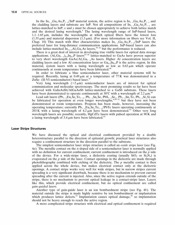
Laser Stripe Structures
We have discussed the optical and electrical confinement provided by a double heterostructure parallel to the direction of epitaxial growth ; practical laser structures also require a confinement structure in the direction parallel to the substrate .
The simplest semiconductor laser stripe structure is called an oxide stripe laser (see Fig . 4 a ) . The metallic contact on the n -doped side of a semiconductor laser is normally applied with no definition for current confinement ; current confinement is introduced on the p side of the device . For a wide-stripe laser , a dielectric coating (usually SiO 2 or Si 3 N 4 ) is evaporated on the p side of the laser . Contact openings in the dielectric are made through photolithography combined with etching of the dielectric . The p metallic contact is then applied across the whole device , but makes electrical contact only at the dielectric openings . A contact stripe works very well for wide stripes , but in narrow stripes current spreading is a very significant drawback , because there is no mechanism to prevent current spreading after the current is injected . Also , since the active region extends outside of the stripe , there is no mechanism to prevent optical leakage in a contact-stripe laser . Lasers like this , which provide electrical confinement , but no optical confinement are called gain - guided lasers .
Another type of gain-guide laser is an ion bombardment stripe (see Fig . 4 b ) . The material outside the stripe is made highly resistive by ion bombardment or implantation which produces lattice defects . 5 5 Implantation causes optical damage , 5 6 so implantation should not be heavy enough to reach the active region .
A more complicated stripe structure with electrical and optical confinement is required
SEMICONDUCTOR LASERS 13 .9
FIGURE 4 Schematic diagrams of GaAs / AlGaAs stripe laser structures . ( a ) Oxide stripe laser ; ( b ) ion bombardment laser , ( c ) buried heterostructure (BH) laser ; ( d ) variation on buried heterostructure laser ; ( e ) ridge waveguide (RWG) laser ; and ( f ) transverse junction stripe (TJS) laser .
for an ef ficient narrow-stripe laser . A number of structures which accomplish the necessary confinement have been developed . These structures are called index - guided lasers , since optical confinement is achieved through a change in refractive index .
The buried heterostructure laser (BH) was first developed by Tsukada . 5 7 To form a BH stripe , a planar laser structure is first grown . Stripe mesas of the laser structure are formed by photolithography combined with etching . For a GaAs-based BH laser , AlGaAs is then
13 .10 OPTICAL SOURCES
regrown around the lasing stripe . Figure 4 c is a schematic diagram of a buried heterostructure . Since the active region is completely surrounded by AlGaAs , a BH has tight optical confinement . If the regrown layers are doped to produce a reverse-biased junction or are semi-insulating , a BH laser can also provide good current confinement . There are many variations on the BH structure . In some cases the active region is grown in the second growth step (see Fig . 4 d ) . The tight optical confinement of BH lasers allows practical fabrication of very narrow stripes , on the order of 1 to 2 m m .
There are many other stripe structures that provide weaker optical confinement than a buried heterostructure . One of the simplest and most widely used of these is the ridge waveguide laser (RWG) (Fig . 4 e ) . After epitaxial growth , most of the p -cladding layer is etched away , leaving a mesa where the lasing stripe will be . Only this mesa is contacted , which provides electrical confinement . The change in surrounding refractive index produces an ef fective change in refractive index in the active region beyond the mesa and provides optical confinement . Other stripe structures are described later in this chapter under ‘‘High-Power Semiconductor Lasers . ’’
Another type of laser stripe is one in which confinement is provided by the p - n junction . The best-known laser of this type is the transverse junction stripe 58 , 59 , 60 (see Fig . 4 f ) . In order to fabricate a TJS laser , both cladding layers are grown as n -AlGaAs . Zn dif fusion is then used to create a p - n junction and contacts are applied on either side of the junction . In this laser the current flows parallel to the substrate rather than perpendicular to it . In a TJS laser the active region is limited to the small region of GaAs in which the Zn dif fusion front ends .
The examples of laser stripe structures described here are GaAs / AlGaAs lasers . Long-wavelength laser structures (InP-based) are very similar , 4 but the active region is InGaAsP and the cladding layers are InP . With an n -InP substrate the substrate can be used as the n -type cladding , which allows greater flexibility in designing structures such as that illustrated in Fig . 4 d . For a more detailed discussion of GaAs-based laser stripe structures see Casey and Panish 2 or Thompson . 3
1 3 . 6 QUANTUM WELL LASERS
The active region in a conventional DH semiconductor laser is wide enough ( , 1000 Å ) that it acts as bulk material and no quantum ef fects are apparent . In such a laser the conduction band and valence band are continuous (Fig . 5 a ) . In bulk material the density of states , D ( E ) , for a transition energy E per unit volume per unit energy is : 2 6
D ( E ) 5 O i 5 l ,h
m i r
π 2 " 3 4 2 m i r ( E 2 E g ) E . E g (2)
where E g is the bandgap energy , " is Plank’s constant divided by 2 π , l and h refer to light and heavy holes , and m r is the ef fective mass of the transition which is defined as :
1 m r
5 1
m c 1
1 m y
(3)
where m c is the conduction band mass and m y is the valence band mass . (The split-of f hole band and the indirect conduction bands are neglected here and have a negligible ef fect on most semiconductor laser calculations . )
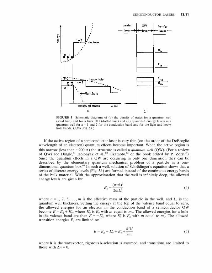
SEMICONDUCTOR LASERS 13 .11
FIGURE 5 Schematic diagrams of ( a ) the density of states for a quantum well (solid line) and for a bulk DH (dotted line) and ( b ) quantized energy levels in a quantum well for n 5 1 and 2 for the conduction band and for the light and heavy hole bands . ( After Ref . 6 3 . )
If the active region of a semiconductor laser is very thin (on the order of the DeBroglie wavelength of an electron) quantum ef fects become important . When the active region is this narrow (less than , 200 Å ) the structure is called a quantum well (QW) . (For a review of QWs see Dingle , 6 1 Holonyak et al ., 6 2 Okamoto , 6 3 or the book edited by P . Zory . 6 4 ) Since the quantum ef fects in a QW are occurring in only one dimension they can be described by the elementary quantum mechanical problem of a particle in a one- dimensional quantum box . 6 5 In such a well , solution of Schro dinger’s equation shows that a series of discrete energy levels (Fig . 5 b ) are formed instead of the continuous energy bands of the bulk material . With the approximation that the well is infinitely deep , the allowed energy levels are given by :
E n 5 ( n π " ) 2
2 mL 2 z
(4)
where n 5 1 , 2 , 3 , . . . , m is the ef fective mass of the particle in the well , and L z is the quantum well thickness . Setting the energy at the top of the valence band equal to zero , the allowed energies for an electron in the conduction band of a semiconductor QW become E 5 E g 1 E c
n , where E c n is E n with m equal to m c . The allowed energies for a hole
in the valence band are then E 5 2 E y n , where E y
n is E n with m equal to m y . The allowed transition energies E , are limited to :
E 5 E g 1 E c n 1 E y
n 1 " 2 k 2
2 m r (5)
where k is the wavevector , rigorous k -selection is assumed , and transitions are limited to those with D n 5 0 .
13 .12 OPTICAL SOURCES
This quantization of energy levels will , of course , change the density of states . For a QW the density of states is given by :
D ( E ) 5 O i 5 l ,h
O n 5 1
m i r
L z π " 2 H ( E 2 E g 2 E c n 2 E y
n ,i ) (6)
where H is the Heavyside function . The dif ference in the density of states directly af fects the modal optical gain generated by the injection of carriers . The modal gain is proportional to the stimulated emission rate : 1 , 66 , 67
g ( E , N ) a G D ( E ) u M u 2 ( f c ( E , N ) 2 f y ( E , N ))
E (7)
where G is the optical confinement factor , u M u 2 is the matrix element for the transition , N is the carrier density of either electrons or holes (the active region is undoped so they have equal densities) , and f c ( E , N ) and f y ( E , N ) are the Fermi occupation factors for the conduction and valence bands . (For a detailed review of gain in semiconductor lasers see Ref . 67 . )
The optical confinement factor G is defined as the ratio of the light intensity of the lasing mode within the active region to the total intensity over all space . Since a QW is very thin , G Q W will be much smaller than G D H . G D H is typically around 0 . 5 whereas for a single QW , G Q W is around 0 . 03 .
The Fermi occupation functions describe the probability that the carriers necessary for stimulated emission have been excited to the states required . They are given by : 1 , 19
f c ( E c , N ) 5 1
1 1 exp (( E g 1 E c 2 F c ) / kT ) (8)
and
f y ( E y , N ) 5 1
1 1 exp ( 2 ( E y 1 F y ) / kT ) (9)
where k is the Boltzmann constant , T is temperature , E c is the energy level of the electron in the conduction band relative to the bottom of the band (including both the quantized energy level and kinetic energy) , E y is the absolute value of the energy level of the hole in a valence band , and F c and F y are the quasi-Fermi levels in the conduction and valence bands . Note that E c and E y are dependent on E , so f c and f y are functions of E . f c and f y are also functions of N through F c and F y . F c and F y are obtained by evaluating the expressions for the electron and hole densities :
N 5 E D c ( E c ) f c ( E c ) dE c (10)
and
N 5 E D y ( E y ) f y ( E y ) dE y (11)
where D c ( E c ) and D y ( E y ) are the densities of states for the conduction and valence bands and follow the same form as D ( E ) for a transition .
SEMICONDUCTOR LASERS 13 .13
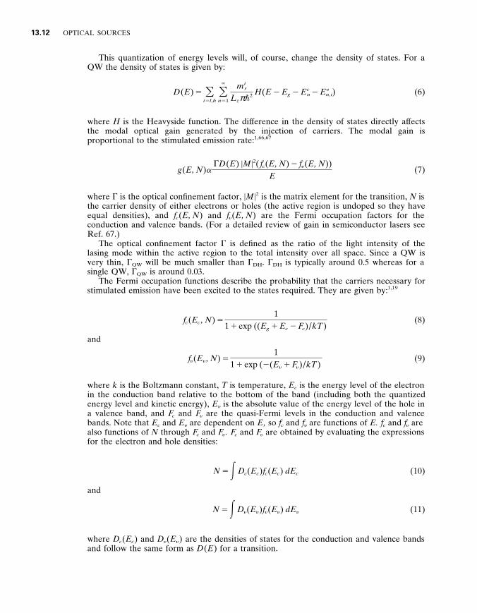
FIGURE 6 Threshold modal gain as a function of threshold carrier density for a conventional (Al , Ga)As double heterostructure with an active region thickness of 1000 Å and for a 100- Å single quantum well . ( From Ref . 6 8 . )
In Fig . 6 , the results of a detailed calculation 6 8 based on Eq . (7) for the threshold modal gain as a function of threshold carrier density are plotted for a 100- Å single QW . The corresponding curve for a DH laser with an active region thickness of 1000 Å is also shown . The gain curves for the QWs are very nonlinear because of saturation of the first quantized state as the carrier density increases . The transparency carrier density N o is the carrier density at which the gain is zero . From Fig . 6 it is clear that the transparency carrier densities for QW and DH lasers are very similar and are on the order of 2 3 10 1 8 cm 2 3 .
The advantage of a QW over a DH laser is not immediately apparent . Consider , however , the transparency current density J o . At transparency 2 8
J o 5 N o L z e
τ s (12)
where L z is the active layer thickness , e is the charge of an electron and τ s is the carrier lifetime near transparency . τ s is approximately 2 to 4 ns for either a QW or a DH laser . Since N o is about the same for either structure , any dif ference in J o will be directly proportional to L z . But L z is approximately ten times smaller for a QW ; therefore , J o will be approximately ten times lower for a QW than for a conventional DH laser . (A lower J o will result in a lower threshold current density since the threshold current density is equal to J o plus a term proportional to the threshold gain . ) Note that this result is not determined by the quantization of energy levels ; it occurs because fewer carriers are needed to reach the same carrier density in a QW as in a DH laser . In other words , this result is achieved because the QW is thin!
In this discussion we are considering current density instead of current . The threshold current density (current divided by the length and width of the stripe) is a more meaningful measure of the relative quality of the lasing material than is current . Current depends very strongly on the geometry and stripe fabrication of the device . In order to
13 .14 OPTICAL SOURCES
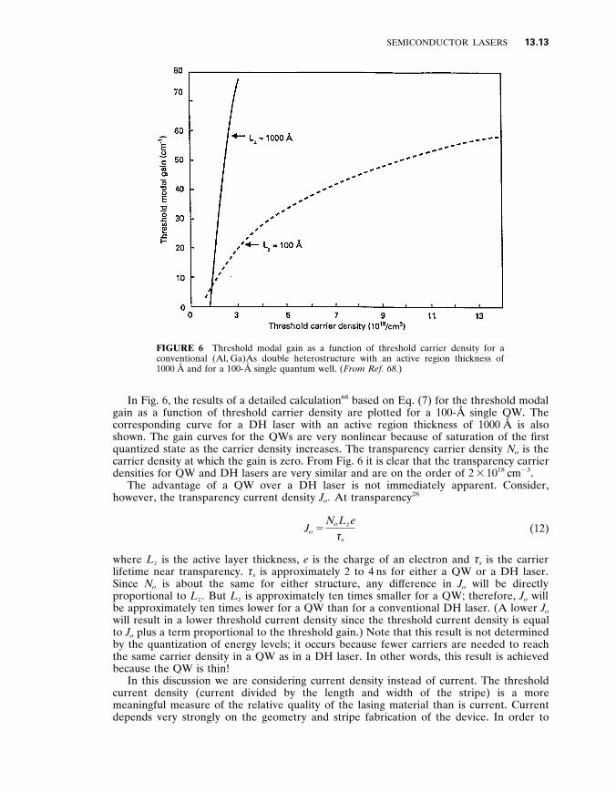
FIGURE 7 Threshold modal gain as a function of threshold current density for a conventional (Al , Ga)As double heterostructure with an active region thickness of 1000 Å and for a 100- Å single quantum well . ( From Ref . 6 8 . )
eliminate geometry-induced variations , current density is normally measured on broad- area (50 – 150 m m wide) oxide stripe lasers (see earlier under ‘‘Fabrication and Configura- tions’’) . With a narrow stripe the current spreads beyond the intended stripe width , so it is dif ficult to accurately measure the current density .
Figure 7 shows the results of a detailed calculation 6 8 of the threshold modal gain versus the threshold current density for a DH laser with an active region thickness of 1000 Å and for a 100- Å single QW . The potential for lower threshold current densities for QW lasers is clear for threshold gains less than that where the curve for the DH laser intercepts those of the QWs . With low losses , the threshold current of a QW laser will be substantially lower than that of a DH laser , since the threshold gain will be below the interception point .
To get an appreciation for how the threshold current density of a single QW will compare to that of a DH laser , consider that near transparency , the modal gain is approximately linearly dependent on the current density :
g ( J ) 5 A ( J 2 J o ) (13)
where A is a constant which should have a similar value for either a QW or a DH laser (this can be seen visually on Fig . 7) . Taking Eq . (13) at threshold we can equate it to Eq . (1) and solve for J t h (the threshold current density) :
J t h 5 J o 1 a i
A 1
1 2 AL
ln S 1 R F R R
D (14)
a i is related primarily to losses occurring through the interaction of the optical mode with the active region . In a QW , the optical confinement is lower , which means that the optical mode interacts less with the active region and a i tends to be smaller . Let’s substitute in the numbers in order to get an idea for the dif ference between a QW and a DH laser . Reasonable values are : 6 9 A Q W , 0 . 7 A 2 1 cm , A D H , 0 . 4 A 2 1 cm , J QW
o , 50 A / cm 2 , J DH o ,
500 A / cm 2 , a QW i , 2 cm 2 1 , a DH
i , 15 cm 2 1 , L , 400 m m , and for uncoated facets R F 5 R R 5 0 . 32 . Substituting in we get : J QW
th , 95 A / cm 2 and J DH th , 610 A / cm 2 .
SEMICONDUCTOR LASERS 13 .15
It is clear that changes in the losses will have a more noticeable ef fect on threshold current for a QW than for a DH laser since losses are responsible for a more significant portion of the threshold current of a QW laser . The gain curve of a QW laser saturates due to the filling of the first quantized energy level , so operating with low losses is even more important for a QW than is illustrated by the above calculation . When the gain saturates , the simple approximation of Eq . (13) is invalid . Operating with low end losses is also important for a QW , since they are a large fraction of the total losses . This explains why threshold current density results for QW lasers are typcially quoted for long laser cavity lengths (greater than 400 m m) , while DH lasers are normally cleaved to lengths on the order of 250 m m . High-quality broad-area single QW lasers (without strain) have threshold current densities lower than 200 A / cm 2 (threshold current densities as low as 93 A / cm 2
have been achieved 69–71 ) , while the very best DH lasers have threshold current densities around 600 A / cm 2 . 7 2 The end loss can also be reduced by the use of high-reflectivity coatings . 2 5 The combination of a single QW active region with a narrow stripe and high-reflectivity coatings has allowed the realization of submilliampere threshold current semiconductor lasers . 68 , 69 , 73 and high-temperature operation . 74 , 75 , 76
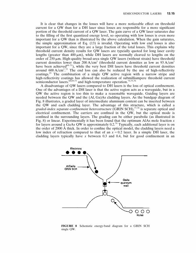
A disadvantage of QW lasers compared to DH lasers is the loss of optical confinement . One of the advantages of a DH laser is that the active region acts as a waveguide , but in a QW the active region is too thin to make a reasonable waveguide . Guiding layers are needed between the QW and the (Al , Ga)As cladding layers . As the bandgap diagram of Fig . 8 illustrates , a graded layer of intermediate aluminum content can be inserted between the QW and each cladding layer . The advantage of this structure , which is called a graded - index separate - confinement heterostructure (GRIN SCH) , 77 , 78 is separate optical and electrical confinement . The carriers are confined in the QW , but the optical mode is confined in the surrounding layers . The grading can be either parabolic (as illustrated in Fig . 8) or linear . Experimentally it has been found that the optimum AlAs mole fraction x for layers around a GaAs QW is approximately 0 . 2 . 7 9 Typically , each additional layer is on the order of 2000 Å thick . In order to confine the optical model , the cladding layers need a low index of refraction compared to that of an x 5 0 . 2 layer . In a simple DH laser , the cladding layers typically have x between 0 . 3 and 0 . 4 , but for good confinement in an
FIGURE 8 Schematic energy-band diagram for a GRIN SCH single QW .
13 .16 OPTICAL SOURCES
x 5 0 . 2 layer , more aluminum should be incorporated into the cladding layers ; x should be between 0 . 5 and 0 . 7 .
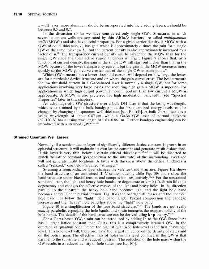
In the discussion so far we have considered only single QWs . Structures in which several quantum wells are separated by thin AlGaAs barriers are called multiquantum wells (MQWs) and also have useful properties . For a given carrier density , a MQW with n QWs of equal thickness , L z has gain which is approximately n times the gain for a single QW of the same thickness L z , but the current density is also approximately increased by a factor of n . 8 0 The transparency current density will be larger for the MQW than for the single QW since the total active region thickness is larger . Figure 9 shows that , as a function of current density , the gain in the single QW will start out higher than that in the MQW because of the lower transparency current , but the gain in the MQW increases more quickly so the MQW gain curve crosses that of the single QW at some point . 8 1
Which QW structure has a lower threshold current will depend on how large the losses are for a particular device structure and on where the gain curves cross . The best structure for low threshold current in a GaAs-based laser is normally a single QW , but for some applications involving very large losses and requiring high gain a MQW is superior . For applications in which high output power is more important than low current a MQW is appropriate . A MQW is also preferred for high modulation bandwidth (see ‘‘Spectral Properties’’ later in this chapter) .
An advantage of a QW structure over a bulk DH laser is that the lasing wavelength , which is determined by the bulk bandgap plus the first quantized energy levels , can be changed by changing the quantum well thickness [see Eq . (4)] . A bulk GaAs laser has a lasing wavelength of about 0 . 87 m m , while a GaAs QW laser of normal thickness (60 – 120 Å ) has a lasing wavelength of 0 . 83 – 0 . 86 m m . Further bandgap engineering can be introduced with a strained QW . 67 , 81 , 82
Strained Quantum Well Lasers
Normally , if a semiconductor layer of significantly dif ferent lattice constant is grown in an epitaxial structure , it will maintain its own lattice constant and generate misfit dislocations . If this layer is very thin , below a certain critical thickness , 81 , 83–85 it will be distorted to match the lattice constant (perpendicular to the substrate) of the surrounding layers and will not generate misfit locations . A layer with thickness above the critical thickness is called ‘‘relaxed , ’’ one below is called ‘‘strained . ’’
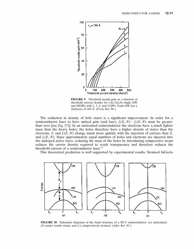
Straining a semiconductor layer changes the valence-band structure . Figure 10 a shows the band structure of an unstrained III-V semiconductor , while Fig . 10 b and c show the band structure under biaxial tension and compression , respectively . 81 , 82 For the unstrained semiconductor , the light and heavy hole bands are degenerate at k 5 0 ( G ) . Strain lifts this degeneracy and changes the ef fective masses of the light and heavy holes . In the direction parallel to the substrate the heavy hole band becomes light and the light hole band becomes heavy . Under biaxial tension (Fig . 10 b ) the bandgap decreases and the ‘‘heavy’’ hole band lies below the ‘‘light’’ hole band . Under biaxial compression the bandgap increases and the ‘‘heavy’’ hole band lies above the ‘‘light’’ hole band .
Figure 10 is a simplification of the true band structure . 81 , 82 The bands are not really exactly parabolic , especially the hole bands , and strain increases the nonparabolicity of the hole bands . The details of the band structure can be derived using k ? p theory . 86–90
For a GaAs based QW , strain can be introduced by adding In to the QW . Since InAs has a larger lattice constant than GaAs , this is a compressively strained QW . In the direction of quantum confinement the highest quantized hole level is the first heavy hole level . This hole level will , therefore , have the largest influence on the density of states and on the optical gain . The ef fective mass of holes in this level confined in the QW is that parallel to the substrate and is reduced by strain . The reduction of the hole mass within the QW results in a reduced density of hole states [see Eq . (6)] .
SEMICONDUCTOR LASERS 13 .17
FIGURE 9 Threshold modal gain as a function of threshold current density for (Al , Ga)As single QW and MQWs with 2 , 3 , 4 , and 5 QWs . Each QW has a thickness of 100 Å . ( From Ref . 8 0 . )
The reduction in density of hole states is a significant improvement . In order for a semiconductor laser to have optical gain (and lase) , f c ( E , N ) 2 f y ( E , N ) must be greater than zero [see Eq . (7)] . In an unstrained semiconductor the electrons have a much lighter mass than the heavy holes ; the holes therefore have a higher density of states than the electrons . F c and f c ( E , N ) change much more quickly with the injection of carriers than F y
and f y ( E , N ) . Since approximately equal numbers of holes and electrons are injected into the undoped active layer , reducing the mass of the holes by introducing compressive strain reduces the carrier density required to reach transparency and therefore reduces the threshold current of a semiconductor laser . 9 1
This theoretical prediction is well supported by experimental results . Strained InGaAs
FIGURE 10 Schematic diagrams of the band structure of a III-V semiconductor : ( a ) unstrained ; ( b ) under tensile strain ; and ( c ) compressively strained . ( After Ref . 8 1 . )
13 .18 OPTICAL SOURCES
single-QW lasers with record-low threshold current densities of 45 to 65 A / cm 2 have been demonstrated . 92–95 These very high quality strained QW lasers typically have lasing wavelengths from 0 . 98 to 1 . 02 m m , QW widths of 60 to 70 Å , and In concentrations of 20 to 25 percent . InGaAs QWs with wavelengths as long as 1 . 1 m m have been successfully fabricated , 96 , 97 but staying below the critical thickness of the InGaAs layers becomes a problem since the wavelength is increased by increasing the In concentration . (With higher In concentration the amount of strain is increased and the critical thickness is reduced . )
Strained InGaAs QWs have another advantage over GaAs QWs . Strained QW lasers are more reliable than GaAs lasers , i . e ., they have longer lifetimes . Even at high temperatures (70 – 100 8 C) , they are very reliable . 75 , 76 The reasons for this are not well understood , but it has been suggested that the strain inhibits the growth of defects in the active region . 98–100 Improving the reliability of GaAs-based lasers is of great practical significance since GaAs lasers are generally less reliable than InP-based lasers . 4 , 101 , 102
Up to this point our discussion of QW lasers has been limited to GaAs-based QW lasers . QW lasers can also be fabricated in other material systems . GaInP / AlGaInP visible lasers have been improved significantly with the use of a single strained QW active region . 103–105 These are also compressively strained QWs formed by adding excess In to the active region . This is a much less developed material system than GaAs , so recent results such as 215 A / cm 2 for a single strained Ga 0 . 43 In 0 . 57 P QW 1 0 3 are very impressive .
Long Wavelength (1 .3 and 1 .55 m m) Quantum Well Lasers
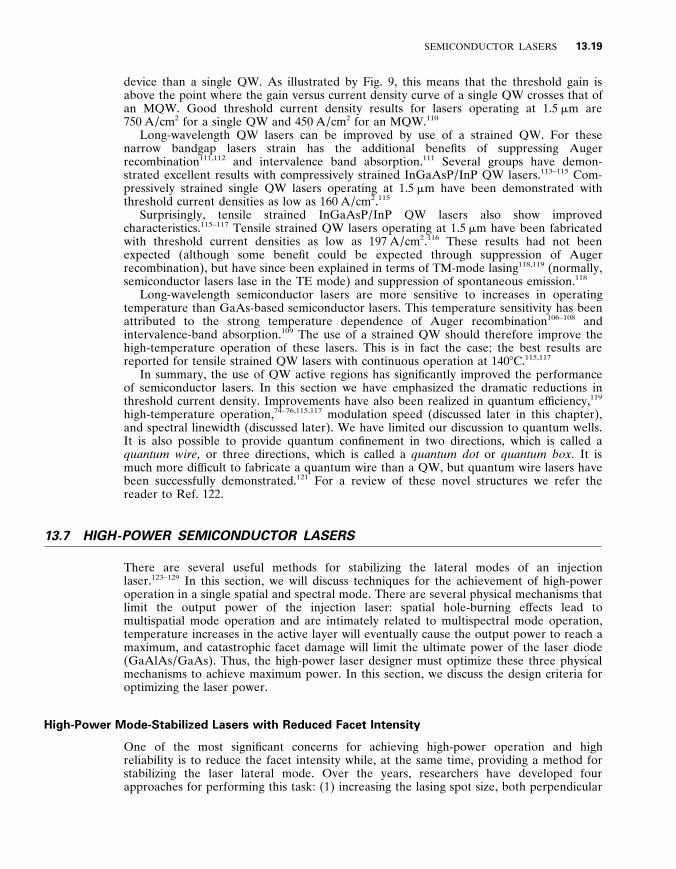
Long wavelength (InGaAsP / InP) QWs generally do not perform as well as GaAs-based QWs ; however , with the advent of strained QW lasers significant progress has been made . Narrow bandgap lasers are believed to be significantly ef fected by nonradiative recombina- tion processes such as Auger recombination 4 , 106–108 and intervalence band absorption . 1 0 9 In Auger recombination (illustrated in Fig . 11) the energy from the recombination of an electron and a hole is transferred to another carrier (either an electron or a hole) . This newly created carrier relaxes by emitting a phonon ; therefore , no photons are created . In intervalence band absorption (IVBA) a photon is emitted , but is reabsorbed to excite a hole from the split-of f band to the heavy hole band . These processes reduce the performance of long wavelength QW lasers enough to make an MQW a lower threshold
FIGURE 11 Schematic diagrams of band-to-band Auger recombination processes . ( After Ref . 4 . )
SEMICONDUCTOR LASERS 13 .19
device than a single QW . As illustrated by Fig . 9 , this means that the threshold gain is above the point where the gain versus current density curve of a single QW crosses that of an MQW . Good threshold current density results for lasers operating at 1 . 5 m m are 750 A / cm 2 for a single QW and 450 A / cm 2 for an MQW . 1 1 0
Long-wavelength QW lasers can be improved by use of a strained QW . For these narrow bandgap lasers strain has the additional benefits of suppressing Auger recombination 111 , 112 and intervalence band absorption . 1 1 1 Several groups have demon- strated excellent results with compressively strained InGaAsP / InP QW lasers . 113–115 Com- pressively strained single QW lasers operating at 1 . 5 m m have been demonstrated with threshold current densities as low as 160 A / cm 2 . 1 1 5
Surprisingly , tensile strained InGaAsP / InP QW lasers also show improved characteristics . 115–117 Tensile strained QW lasers operating at 1 . 5 m m have been fabricated with threshold current densities as low as 197 A / cm 2 . 1 1 6 These results had not been expected (although some benefit could be expected through suppression of Auger recombination) , but have since been explained in terms of TM-mode lasing 118 , 119 (normally , semiconductor lasers lase in the TE mode) and suppression of spontaneous emission . 1 1 8
Long-wavelength semiconductor lasers are more sensitive to increases in operating temperature than GaAs-based semiconductor lasers . This temperature sensitivity has been attributed to the strong temperature dependence of Auger recombination 106–108 and intervalence-band absorption . 1 0 9 The use of a strained QW should therefore improve the high-temperature operation of these lasers . This is in fact the case ; the best results are reported for tensile strained QW lasers with continuous operation at 140 8 C . 115 , 117
In summary , the use of QW active regions has significantly improved the performance of semiconductor lasers . In this section we have emphasized the dramatic reductions in threshold current density . Improvements have also been realized in quantum ef ficiency , 1 1 9
high-temperature operation , 74–76 , 115 , 117 modulation speed (discussed later in this chapter) , and spectral linewidth (discussed later) . We have limited our discussion to quantum wells . It is also possible to provide quantum confinement in two directions , which is called a quantum wire , or three directions , which is called a quantum dot or quantum box . It is much more dif ficult to fabricate a quantum wire than a QW , but quantum wire lasers have been successfully demonstrated . 1 2 1 For a review of these novel structures we refer the reader to Ref . 122 .
1 3 . 7 HIGH - POWER SEMICONDUCTOR LASERS
There are several useful methods for stabilizing the lateral modes of an injection laser . 123–129 In this section , we will discuss techniques for the achievement of high-power operation in a single spatial and spectral mode . There are several physical mechanisms that limit the output power of the injection laser : spatial hole-burning ef fects lead to multispatial mode operation and are intimately related to multispectral mode operation , temperature increases in the active layer will eventually cause the output power to reach a maximum , and catastrophic facet damage will limit the ultimate power of the laser diode (GaAlAs / GaAs) . Thus , the high-power laser designer must optimize these three physical mechanisms to achieve maximum power . In this section , we discuss the design criteria for optimizing the laser power .
High-Power Mode-Stabilized Lasers with Reduced Facet Intensity
One of the most significant concerns for achieving high-power operation and high reliability is to reduce the facet intensity while , at the same time , providing a method for stabilizing the laser lateral mode . Over the years , researchers have developed four approaches for performing this task : (1) increasing the lasing spot size , both perpendicular
13 .20 OPTICAL SOURCES
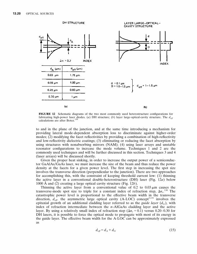
FIGURE 12 Schematic diagrams of the two most commonly used heterostructure configurations for fabricating high-power laser diodes . ( a ) DH structure ; ( b ) layer large-optical-cavity structure . The d ef f calculations are after Botez . 1 3 0
to and in the plane of the junction , and at the same time introducing a mechanism for providing lateral mode-dependent absorption loss to discriminate against higher-order modes ; (2) modifying the facet reflectivities by providing a combination of high-reflectivity and low-reflectivity dielectric coatings ; (3) eliminating or reducing the facet absorption by using structures with nonabsorbing mirrors (NAM) ; (4) using laser arrays and unstable resonator configurations to increase the mode volume . Techniques 1 and 2 are the commonly used techniques and will be further discussed in this section . Techniques 3 and 4 (laser arrays) will be discussed shortly .
Given the proper heat sinking , in order to increase the output power of a semiconduc- tor GaAlAs / GaAs laser , we must increase the size of the beam and thus reduce the power density at the facets for a given power level . The first step in increasing the spot size involves the transverse direction (perpendicular to the junction) . There are two approaches for accomplishing this , with the constraint of keeping threshold current low : (1) thinning the active layer in a conventional double-heterostructure (DH) laser (Fig . 12 a ) below 1000 Å and (2) creating a large optical cavity structure (Fig . 12 b ) .
Thinning the active layer from a conventional value of 0 . 2 to 0 . 03 m m causes the transverse-mode spot size to triple for a constant index of refraction step , D n r .
1 3 0 The catastrophic power level is proportional to the ef fective beam width in the transverse direction , d ef f . the asymmetric large optical cavity (A-LOC) concept 3 , 131 involves the epitaxial growth of an additional cladding layer referred to as the guide layer ( d G ) , with index of refraction intermediate between the n -AlGaAs cladding layer and the active layer . By using a relatively small index of refraction step ( D n r 5 0 . 1) versus 0 . 20 – 0 . 30 for DH lasers , it is possible to force the optical mode to propagate with most of its energy in the guide layer . The ef fective beam width for the A-LOC can be approximately expressed as
d ef f 5 d A 1 d G (15)
SEMICONDUCTOR LASERS 13 .21
where d A is the active layer thickness . Mode spot sizes in the transverse direction of approximately 1 . 5 m m can be achieved .
Important Commercial High-Power Diode Lasers
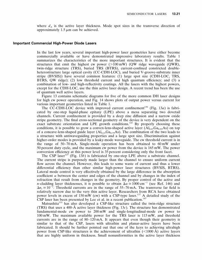
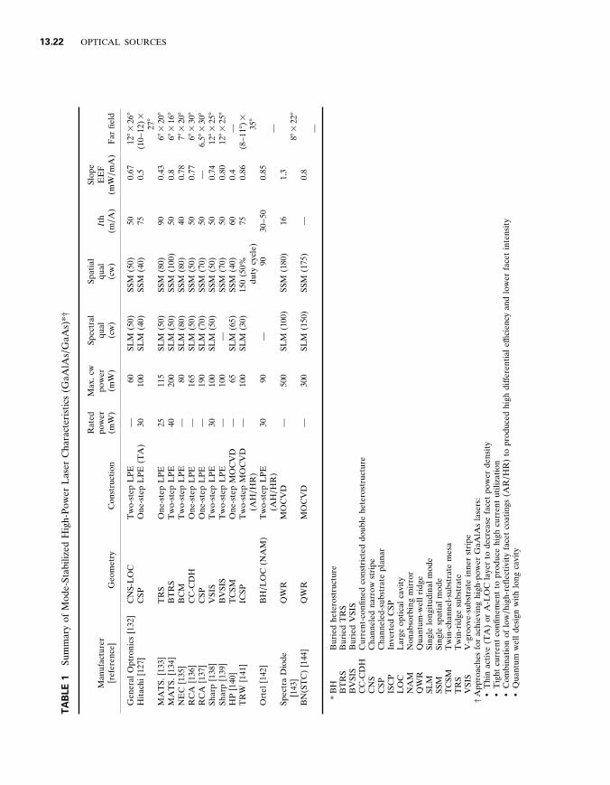
In the last few years , several important high-power laser geometries have either become commercially available or have demonstrated impressive laboratory results . Table 1 summarizes the characteristics of the more important structures . It is evident that the structures that emit the highest cw power ( . 100 mW) (QW ridge waveguide (QWR) , twin-ridge structure (TRS) , buried TRS (BTRS) , current-confined constricted double- heterostructure large optical cavity (CC-CDH-LOC) , and buried V-groove-substrate inner stripe (BVSIS)) have several common features : (1) large spot size (CDH-LOC , TRS , BTRS , QW ridge) ; (2) low threshold current and high quantum ef ficiency ; and (3) a combination of low- and high-reflectivity coatings . All the lasers with the highest powers , except for the CDH-LOC , use the thin active laser design . A recent trend has been the use of quantum well active layers .
Figure 13 contains schematic diagrams for five of the more common DH laser designs for high cw power operation , and Fig . 14 shows plots of output power versus current for various important geometries listed in Table 1 .
The CC-CDH-LOC device with improved current confinement 1 3 6 (Fig . 13 a ) is fabri- cated by one-step liquid-phase epitaxy (LPE) above a mesa separating two dovetail channels . Current confinement is provided by a deep zinc dif fusion and a narrow oxide stripe geometry . The final cross-sectional geometry of the device is very dependent on the exact substrate orientation and LPE growth conditions . 1 4 5 By properly choosing these conditions , it is possible to grow a convex-lens-shaped active layer (Al 0 . 07 Ga 0 . 93 As) on top of a concave-lens-shaped guide layer (Al 0 . 21 Ga 0 . 79 As) . The combination of the two leads to a structure with antiwaveguiding properties and a large spot size . Discrimination against higher-order modes is provided by a leaky-mode waveguide . The cw threshold current is in the range of 50 – 70 mA . Single-mode operation has been obtained to 60 mW under 50 percent duty cycle , and the maximum cw power from the device is 165 mW . The power conversion ef ficiency at this power level is 35 percent considering only the front facet .
The CSP laser 1 2 7 (Fig . 13 b ) is fabricated by one-step LPE above a substrate channel . The current stripe is purposely made larger than the channel to ensure uniform current flow across the channel . However , this leads to some waste of current and thus a lower dif ferential ef ficiency than other similar high-power laser structures (BVSIS , BTRS) . Lateral mode control is very ef fectively obtained by the large dif ference in the absorption coef ficient a between the center and edges of the channel and by changes in the index of refraction that result from changes in the geometry . By proper control of the active and n -cladding layer thicknesses , it is possible to obtain D a > 1000 cm 2 1 (see Ref . 146) and D n r > 10 2 2 . Threshold currents are in the range of 55 – 70 mA . The transverse far field is relatively narrow due to the very thin active layer . Researchers from RCA have obtained power levels in excess of 150 mW (cw) with a CSP-type laser . 1 3 7 A detailed study of the CSP laser has been presented by Lee et al . in a recent publication . 1 4 7
Matsushita 1 3 3 has also developed a CSP-like structure called the twin-ridge structure (TRS) that uses a 400- Å active layer thickness (Fig . 13 c ) . The structure has demonstrated fundamental-mode cw power to 200 mW and single-longitudinal-mode cw power to 100 mW . The maximum available power for the TRS laser is 115 mW , and threshold currents are in the range of 80 – 120 mA . It appears that even though their geometry is similar to that of the CSP , lasers with ultrathin and planar-active layers have been fabricated . It should be further pointed out that one of the keys to achieving ultrahigh power from CSP-like structures is the achievement of ultrathin ( , 1000 Å ) active layers that are highly uniform in thickness . Small nonuniformities in the active layer thickness
13 .22 OPTICAL SOURCES
TA
BLE
1 Su
mm
ary
of M
ode-
Stab
ilize
d H
igh-
Pow
er L
aser
Cha
ract
eris
tics
(G
aAlA
s / G
aAs)
* †
Man
ufac
ture
r [r
efer
ence
] G
eom
etry
Con
stru
ctio
n
Rat
ed po
wer
(mW
)
Max
. cw
pow
er (m
W)
Spec
tral
qual
(cw
)
Spat
ial
qual
(cw
) I t
h (m
/ A)
Slop
e E
EF
(mW
/ mA
) F
ar fi
eld
Gen
eral
Opt
roni
cs [
132]
CN
S-L
OC
Tw
o-st
ep L
PE
— 60
SLM
(50
) SS
M (
50)
50 0 .
67 12
8 3
26 8
Hit
achi
[12
7] C
SP O
ne-s
tep
LP
E (
TA
) 30
100
SLM
(40
) SS
M (
40)
75 0 .
5 (1
0 – 12
) 3 27
8 M
AT
S . [
133]
MA
TS .
[13
4] N
EC
[13
5] R
CA
[13
6] R
CA
[13
7] Sh
arp
[138
] Sh
arp
[139
] H
P [
140]
TR
S B
TR
S B
CM
CC
-CD
H C
SP V
SIS
BV
SIS
TC
SM
One
-ste
p L
PE
Tw
o-st
ep L
PE
Tw
o-st
ep L
PE
One
-ste
p L
PE
One
-ste
p L
PE
Tw
o-st
ep L
PE
Tw
o-st
ep L
PE
One
-ste
p M
OC
VD
25 40 — — — 30 — —
115
200 80 165
190
100
100 65
SLM
(50
) SL
M (
50)
SLM
(80
) SL
M (
50)
SLM
(70
) SL
M (
50)
— SL
M (
65)
SSM
(80
) SS
M (
100)
SSM
(80
) SS
M (
50)
SSM
(70
) SS
M (
50)
SSM
(70
) SS
M (
40)
90 50 40 50 50 50 50 60
0 . 43
0 . 8
0 . 78
0 . 77
— 0 . 74
0 . 80
0 . 4
6 8 3
20 8
6 8 3
16 8
7 8 3
20 8
6 8 3
30 8
6 . 5 8
3 30
8 12
8 3
25 8
12 8
3 25
8 —
TR
W [
141]
Ort
el [
142]
Spec
tra
Dio
de [1
43]
BN
(ST
C)
[144
]
ICSP
BH
/ LO
C (
NA
M)
QW
R
QW
R
Tw
o-st
ep M
OC
VD
(AH
/ HR
) T
wo-
step
LP
E (A
H / H
R)
MO
CV
D
MO
CV
D
— 30 — —
100 90 500
300
SLM
(30
)
—
SLM
(10
0)
SLM
(15
0)
150
(50%
duty
cyc
le)
90
SSM
(18
0)
SSM
(17
5)
75
30 – 5
0
16 —
0 . 86
0 . 85
1 . 3
0 . 8
(8 – 1
1 8 ) 3 35
8
—
8 8 3
22 8
—
* B
H B
urie
d he
tero
stru
ctur
e B
TR
S B
urie
d T
RS
BV
SIS
Bur
ied
VSI
S C
C-C
DH
Cur
rent
-con
fined
cons
tric
ted
doub
le he
tero
stru
ctur
e C
NS
Cha
nnel
ed na
rrow
stri
pe C
SP C
hann
eled
-sub
stra
te pl
anar
ISC
P In
vert
ed C
SP L
OC
Lar
ge op
tica
l ca
vity
NA
M N
onab
sorb
ing
mir
ror
QW
R Q
uant
um-w
ell
ridg
e SL
M Si
ngle
long
itud
inal
mod
e SS
M Si
ngle
spat
ial
mod
e T
CSM
Tw
in-c
hann
el-s
ubst
rate
mes
a T
RS
Tw
in-r
idge
subs
trat
e V
SIS
V-g
roov
e-su
bstr
ate
inne
r st
ripe
† A
ppro
ache
s fo
r ac
hiev
ing
high
-pow
er G
aAlA
s la
sers
: $
Thi
n ac
tive
(T
A)
or A
-LO
C l
ayer
to
decr
ease
fac
et p
ower
den
sity
$ T
ight
cur
rent
con
finem
ent
to p
rodu
ce h
igh
curr
ent
utili
zati
on $
Com
bina
tion
of
low
/ hig
h-re
flect
ivit
y fa
cet
coat
ings
(A
R / H
R)
to p
rodu
ced
high
dif f
eren
tial
ef fi
cien
cy a
nd l
ower
fac
et i
nten
sity
$ Q
uant
um w
ell
desi
gn w
ith
long
cav
ity
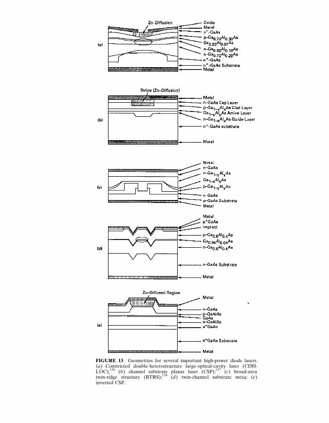
FIGURE 13 Geometries for several important high-power diode lasers . ( a ) Constricted double-heterostructure large-optical-cavity laser (CDH- LOC) ; 1 3 6 ( b ) channel substrate planar laser (CSP) ; 1 2 7 ( c ) broad-area twin-ridge structure (BTRS) ; 1 3 4 ( d ) twin-channel substrate mesa ; ( e ) inverted CSP .
13 .24 OPTICAL SOURCES
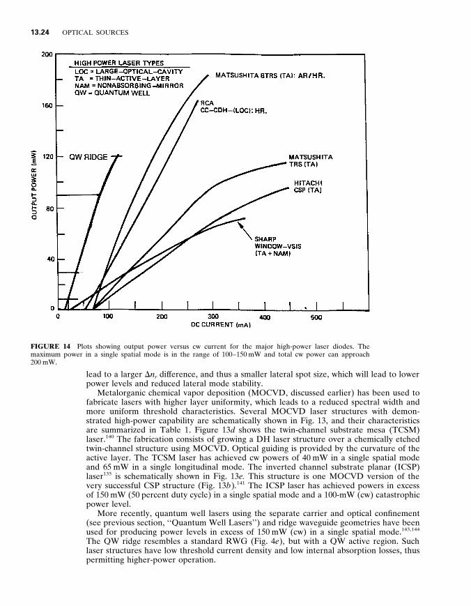
FIGURE 14 Plots showing output power versus cw current for the major high-power laser diodes . The maximum power in a single spatial mode is in the range of 100 – 150 mW and total cw power can approach 200 mW .
lead to a larger D n r dif ference , and thus a smaller lateral spot size , which will lead to lower power levels and reduced lateral mode stability .
Metalorganic chemical vapor deposition (MOCVD , discussed earlier) has been used to fabricate lasers with higher layer uniformity , which leads to a reduced spectral width and more uniform threshold characteristics . Several MOCVD laser structures with demon- strated high-power capability are schematically shown in Fig . 13 , and their characteristics are summarized in Table 1 . Figure 13 d shows the twin-channel substrate mesa (TCSM) laser . 1 4 0 The fabrication consists of growing a DH laser structure over a chemically etched twin-channel structure using MOCVD . Optical guiding is provided by the curvature of the active layer . The TCSM laser has achieved cw powers of 40 mW in a single spatial mode and 65 mW in a single longitudinal mode . The inverted channel substrate planar (ICSP) laser 1 3 5 is schematically shown in Fig . 13 e . This structure is one MOCVD version of the very successful CSP structure (Fig . 13 b ) . 1 4 1 The ICSP laser has achieved powers in excess of 150 mW (50 percent duty cycle) in a single spatial mode and a 100-mW (cw) catastrophic power level .
More recently , quantum well lasers using the separate carrier and optical confinement (see previous section , ‘‘Quantum Well Lasers’’) and ridge waveguide geometries have been used for producing power levels in excess of 150 mW (cw) in a single spatial mode . 143 , 144
The QW ridge resembles a standard RWG (Fig . 4 e ) , but with a QW active region . Such laser structures have low threshold current density and low internal absorption losses , thus permitting higher-power operation .
SEMICONDUCTOR LASERS 13 .25
Future Directions for High-Power Lasers
Nonabsorbing Mirror Technology . The catastrophic facet damage is the ultimate limit to the power from a semiconductor laser . In order to prevent catastrophic damage , one has to create a region of higher-energy bandgap and low surface recombination at the laser facets . Thus , the concept of a laser with a nonabsorbing mirror (NAM) was developed . The first NAM structure was demonstrated by Yonezu et al . 1 4 8 by selectively dif fusing zinc along the length of the stripe , except near the facets . This created a bandgap dif ference between the facet and bulk regions and permitted a three- to fourfold increase in the cw facet damage threshold and a four- to fivefold increase in pulse power operation . 1 4 9 More recent structures have involved several steps of liquid-phase epitaxy . 150 , 151
The incorporation of the NAM structure is strongly device-dependent . For example , in the dif fused device structures , such as deep-dif fused stripe (DDS) 1 4 8 and transverse junction stripe (TJS) lasers , NAM structures have been formed by selective dif fusion of zinc in the cavity direction . 1 4 9 The n -type region will have a wider bandgap than the dif fused region , and thus there will be little absorption near the facets . However , most index-guided structures require an additional growth step for forming the NAM region . 150 , 151 the NAM structures in the past have suf fered from several problems : (1) Due to their complex fabrication , they tend to have low yields . Furthermore , cw operation has been dif ficult to obtain . (2) Cleaving must be carefully controlled for NAM structures having no lateral confinement , in order to avoid excessive radiation losses in the NAM region . The NAM length is a function of the spot size . (3) The ef fect of the NAM structure on lateral mode control has not been documented , but could lead to excessive scattering and a rough far-field pattern .
It is now becoming more clear that the use of a NAM structure will be required for the reliable operation of high-power GaAlAs / GaAs laser diodes . Experimental results 1 5 2
appear to indicate that laser structures without a NAM region show a decrease in the catastrophic power level as the device degrades . However , most of the approaches currently being implemented require elaborate processing steps . A potentially more fundamental approach would involve the deposition of a coating that would reduce the surface recombination velocity and thus enhance the catastrophic intensity level . 153 , 154 Such coatings have been recently used by researchers from Sharp and the University of Florida to increase the uncoated facet catastrophic power level by a factor of 2 . 155 , 156
Recently , the use of NAM technology has been appearing in commercial products . The crank transverse junction stripe (TJS) laser (a TJS laser with NAM) can operate reliably at an output power of 15 mW (cw) , while the TJS laser without the NAM can operate only at 3 mW (cw) . 1 4 7 The Ortel Corporation has developed a buried heterostructure (BH) laser with significantly improved output power characteristics compared to conventional BH lasers . 1 4 2 The NAM BH laser is rated at 30 mW (cw) 1 4 2 compared to 3 – 10 mW for the conventional BH / LOC device .
Last , the use of alloy disordering , whereby the bandgap of a quantum well laser can be increased by dif fusion of various types of impurities (for example , Zn and Si) , 1 5 7 can lead to a very ef fective technique for the fabrication of a NAM structure . Such structures have produced an enhancement of the maximum pulsed power by a factor of 3 – 4 .
High - Power 1 . 3 / 1 . 4 8 / 1 . 5 5 - m m Lasers . Previous sections have discussed high cw power operation from (GaAl)As / GaAs laser devices . In the past several years there have been reports of the increasing power levels achieved with GaInAsP / InP lasers operating at l 5 1 . 3 m m . The physical mechanisms limiting high-power operation in this material system are quite dif ferent than those for GaAlAs / GaAs lasers . The surface recombination at the laser facets is significantly lower than in GaAlAs / GaAs , and thus catastrophic damage has not been observed . Maximum output power is limited by either heating or carrier leakage ef fects . With the advent of structures having low threshold current density and high quantum ef ficiency , it was just a matter of time before high-power results would become
13 .26 OPTICAL SOURCES
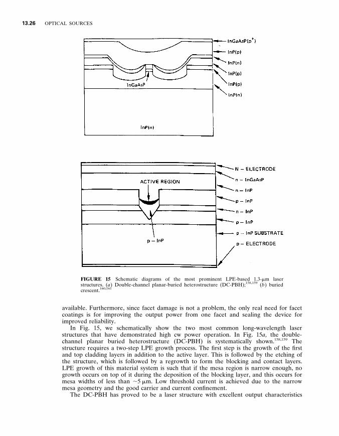
FIGURE 15 Schematic diagrams of the most prominent LPE-based 1 . 3- m m laser structures . ( a ) Double-channel planar-buried heterostructure (DC-PBH) ; 158 , 159 ( b ) buried crescent . 160 , 161
available . Furthermore , since facet damage is not a problem , the only real need for facet coatings is for improving the output power from one facet and sealing the device for improved reliability .
In Fig . 15 , we schematically show the two most common long-wavelength laser structures that have demonstrated high cw power operation . In Fig . 15 a , the double- channel planar buried heterostructure (DC-PBH) is systematically shown . 158 , 159 The structure requires a two-step LPE growth process . The first step is the growth of the first and top cladding layers in addition to the active layer . This is followed by the etching of the structure , which is followed by a regrowth to form the blocking and contact layers . LPE growth of this material system is such that if the mesa region is narrow enough , no growth occurs on top of it during the deposition of the blocking layer , and this occurs for mesa widths of less than , 5 m m . Low threshold current is achieved due to the narrow mesa geometry and the good carrier and current confinement .
The DC-PBH has proved to be a laser structure with excellent output characteristics
SEMICONDUCTOR LASERS 13 .27
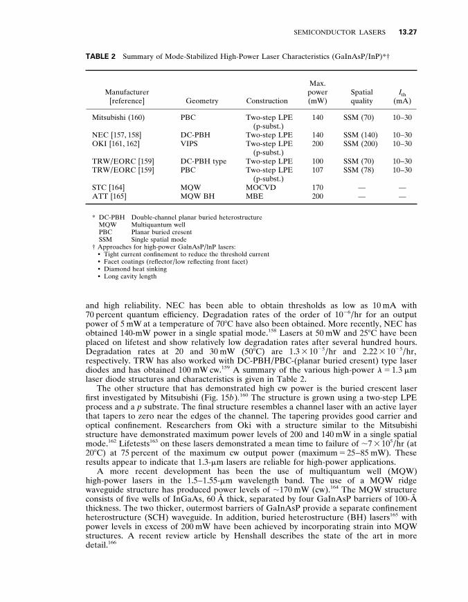
TABLE 2 Summary of Mode-Stabilized High-Power Laser Characteristics (GaInAsP / InP)* †
Manufacturer [reference] Geometry Construction
Max . power (mW)
Spatial quality
I t h (mA)
Mitsubishi (160) PBC Two-step LPE (p-subst . )
140 SSM (70) 10 – 30
NEC [157 , 158] DC-PBH Two-step LPE 140 SSM (140) 10 – 30 OKI [161 , 162] VIPS Two-step LPE
(p-subst . ) 200 SSM (200) 10 – 30
TRW / EORC [159] DC-PBH type Two-step LPE 100 SSM (70) 10 – 30 TRW / EORC [159] PBC Two-step LPE
(p-subst . ) 107 SSM (78) 10 – 30
STC [164] ATT [165]
MQW MQW BH
MOCVD MBE
170 200
— —
— —
* DC-PBH Double-channel planar buried heterostructure MQW Multiquantum well PBC Planar buried cresent SSM Single spatial mode
† Approaches for high-power GalnAsP / lnP lasers : $ Tight current confinement to reduce the threshold current $ Facet coatings (reflector / low reflecting front facet) $ Diamond heat sinking $ Long cavity length
and high reliability . NEC has been able to obtain thresholds as low as 10 mA with 70 percent quantum ef ficiency . Degradation rates of the order of 10 2 6 / hr for an output power of 5 mW at a temperature of 70 8 C have also been obtained . More recently , NEC has obtained 140-mW power in a single spatial mode . 1 5 8 Lasers at 50 mW and 25 8 C have been placed on lifetest and show relatively low degradation rates after several hundred hours . Degradation rates at 20 and 30 mW (50 8 C) are 1 . 3 3 10 2 5 / hr and 2 . 22 3 10 2 5 / hr , respectively . TRW has also worked with DC-PBH / PBC-(planar buried cresent) type laser diodes and has obtained 100 mW cw . 1 5 9 A summary of the various high-power l 5 1 . 3 m m laser diode structures and characteristics is given in Table 2 .
The other structure that has demonstrated high cw power is the buried crescent laser first investigated by Mitsubishi (Fig . 15 b ) . 1 6 0 The structure is grown using a two-step LPE process and a p substrate . The final structure resembles a channel laser with an active layer that tapers to zero near the edges of the channel . The tapering provides good carrier and optical confinement . Researchers from Oki with a structure similar to the Mitsubishi structure have demonstrated maximum power levels of 200 and 140 mW in a single spatial mode . 1 6 2 Lifetests 1 6 3 on these lasers demonstrated a mean time to failure of , 7 3 10 5 / hr (at 20 8 C) at 75 percent of the maximum cw output power (maximum 5 25 – 85 mW) . These results appear to indicate that 1 . 3- m m lasers are reliable for high-power applications .
A more recent development has been the use of multiquantum well (MQW) high-power lasers in the 1 . 5 – 1 . 55- m m wavelength band . The use of a MQW ridge waveguide structure has produced power levels of , 170 mW (cw) . 1 6 4 The MQW structure consists of five wells of InGaAs , 60 Å thick , separated by four GaInAsP barriers of 100- Å thickness . The two thicker , outermost barriers of GaInAsP provide a separate confinement heterostructure (SCH) waveguide . In addition , buried heterostructure (BH) lasers 1 6 5 with power levels in excess of 200 mW have been achieved by incorporating strain into MQW structures . A recent review article by Henshall describes the state of the art in more detail . 1 6 6
13 .28 OPTICAL SOURCES
TABLE 3 High-Power GaInAs Strained Layer Quantum-Well Lasers
Laser group [reference]
Ridge width ( m m)
Wavelength ( m m)
Threshold current (mA)
Max . power in single
spatial mode (mW)
Max . cw power (mW)
JPL [168] JPL [168] NTT [169] Spectra Diode [170] Boeing [76]
6 3 3 4 4
0 . 984 – 0 . 989 0 . 978
0 . 973 – 0 . 983 0 . 9 – 0 . 91
0 . 98
13 8 9
, 20 10 – 15
— 116 115 180 150
24 400 500 350 440
High - Power Strained Quantum Well Lasers . Over the last several years , there has been extensive research in the area of strained layer quantum well high-power lasers . As with GaAs QW high-power lasers , the geometry is typically a QW ridge . Table 3 summarizes some of the latest single-spatial-mode high-power results .
Thermal Properties . An important parameter in the operation of high-power laser diodes is the optimization of thermal properties of the device . In particular , optimizing the laser geometry for achieving high-power operation is an important design criterion . Arvind et al . 1 6 7 used a simple one-dimensional thermal model for estimating the maximum output power as a function of laser geometry (cavity length , active layer thickness substrate type , etc . ) . The results obtained for GaInAsP / InP narrow stripe PH lasers were as follows :
$ Maximum output power is achieved for an optimum active layer thickness in the 0 . 15- m m region . This result applies only to nonquantum well lasers .
$ Significantly higher output powers (25 to 60 percent) are obtained for lasers fabricated on p substrates compared to those on n substrates . The result is based on the lower electrical resistance of the top epitaxial layers in the p substrate compared to n substrate .
$ Significantly higher output powers ( , 60 percent) are obtained for lasers mounted on diamond rather than silicon heat sinks as a result of the higher thermal conductivity of diamond compared to silicon , 22 versus 1 . 3 W / ( 8 C-cm) .
$ Significantly higher output powers ( , 100 percent) are obtained for lasers having a length of 700 m m compared to the conventional 300 m m . The higher power results from the reduced threshold current density and thermal resistance for the longer laser devices .
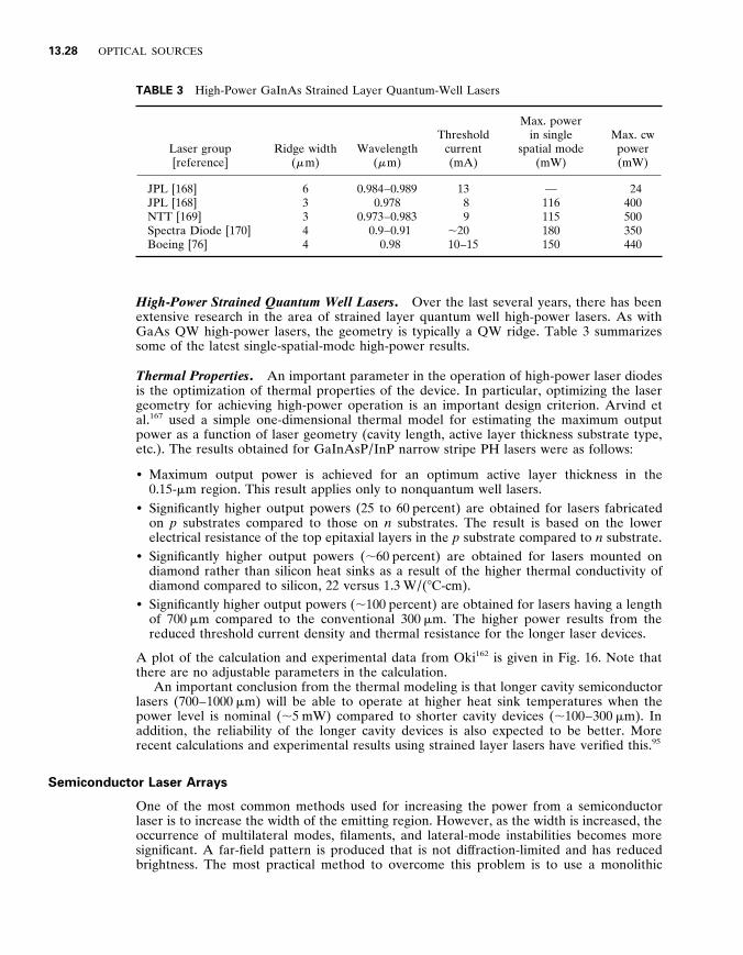
A plot of the calculation and experimental data from Oki 1 6 2 is given in Fig . 16 . Note that there are no adjustable parameters in the calculation .
An important conclusion from the thermal modeling is that longer cavity semiconductor lasers (700 – 1000 m m) will be able to operate at higher heat sink temperatures when the power level is nominal ( , 5 mW) compared to shorter cavity devices ( , 100 – 300 m m) . In addition , the reliability of the longer cavity devices is also expected to be better . More recent calculations and experimental results using strained layer lasers have verified this . 9 5
Semiconductor Laser Arrays
One of the most common methods used for increasing the power from a semiconductor laser is to increase the width of the emitting region . However , as the width is increased , the occurrence of multilateral modes , filaments , and lateral-mode instabilities becomes more significant . A far-field pattern is produced that is not dif fraction-limited and has reduced brightness . The most practical method to overcome this problem is to use a monolithic
SEMICONDUCTOR LASERS 13 .29
FIGURE 16 Calculation of maximum output power per facet as a function of device length for n - p -substrate-type lasers and dif ferent heat sinks . 1 6 7 Note the increased power level achieved for longer lasers and p -type substrates .
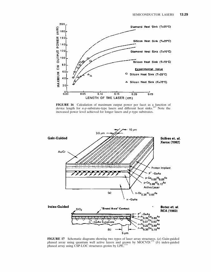
FIGURE 17 Schematic diagrams showing two types of laser array structures . ( a ) Gain-guided phased array using quantum well active layers and grown by MOCVD : 1 7 5 ( b ) index-guided phased array using CSP-LOC structures grown by LPE . 1 7 3
13 .30 OPTICAL SOURCES
TABLE 4 Summary of High-Power Phase-Locked Laser Arrays*
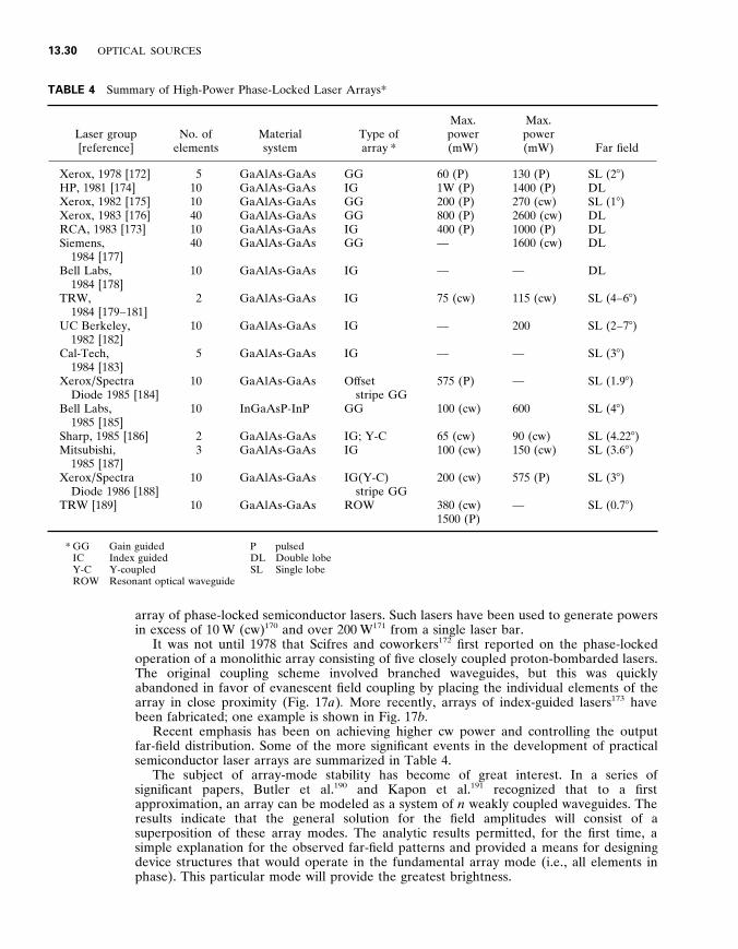
Laser group [reference]
No . of elements
Material system
Type of array *
Max . power (mW)
Max . power (mW) Far field
Xerox , 1978 [172] HP , 1981 [174] Xerox , 1982 [175] Xerox , 1983 [176] RCA , 1983 [173]
5 10 10 40 10
GaAlAs-GaAs GaAlAs-GaAs GaAlAs-GaAs GaAlAs-GaAs GaAlAs-GaAs
GG IG GG GG IG
60 (P) 1W (P) 200 (P) 800 (P) 400 (P)
130 (P) 1400 (P) 270 (cw) 2600 (cw) 1000 (P)
SL (2 8 ) DL SL (1 8 ) DL DL
Siemens , 1984 [177]
Bell Labs , 1984 [178]
TRW , 1984 [179 – 181]
UC Berkeley , 1982 [182]
Cal-Tech , 1984 [183]
40
10
2
10
5
GaAlAs-GaAs
GaAlAs-GaAs
GaAlAs-GaAs
GaAlAs-GaAs
GaAlAs-GaAs
GG
IG
IG
IG
IG
—
—
75 (cw)
—
—
1600 (cw)
—
115 (cw)
200
—
DL
DL
SL (4 – 6 8 )
SL (2 – 7 8 )
SL (3 8 )
Xerox / Spectra Diode 1985 [184]
Bell Labs , 1985 [185]
Sharp , 1985 [186]
10
10
2
GaAlAs-GaAs
InGaAsP-InP
GaAlAs-GaAs
Of fset stripe GG
GG
IG ; Y-C
575 (P)
100 (cw)
65 (cw)
—
600
90 (cw)
SL (1 . 9 8 )
SL (4 8 )
SL (4 . 22 8 ) Mitsubishi ,
1985 [187] Xerox / Spectra
Diode 1986 [188] TRW [189]
3
10
10
GaAlAs-GaAs
GaAlAs-GaAs
GaAlAs-GaAs
IG
IG(Y-C) stripe GG
ROW
100 (cw)
200 (cw)
380 (cw) 1500 (P)
150 (cw)
575 (P)
—
SL (3 . 6 8 )
SL (3 8 )
SL (0 . 7 8 )
* GG Gain guided P pulsed IC Index guided DL Double lobe Y-C Y-coupled SL Single lobe ROW Resonant optical waveguide
array of phase-locked semiconductor lasers . Such lasers have been used to generate powers in excess of 10 W (cw) 1 7 0 and over 200 W 1 7 1 from a single laser bar .
It was not until 1978 that Scifres and coworkers 1 7 2 first reported on the phase-locked operation of a monolithic array consisting of five closely coupled proton-bombarded lasers . The original coupling scheme involved branched waveguides , but this was quickly abandoned in favor of evanescent field coupling by placing the individual elements of the array in close proximity (Fig . 17 a ) . More recently , arrays of index-guided lasers 1 7 3 have been fabricated ; one example is shown in Fig . 17 b .
Recent emphasis has been on achieving higher cw power and controlling the output far-field distribution . Some of the more significant events in the development of practical semiconductor laser arrays are summarized in Table 4 .
The subject of array-mode stability has become of great interest . In a series of significant papers , Butler et al . 1 9 0 and Kapon et al . 1 9 1 recognized that to a first approximation , an array can be modeled as a system of n weakly coupled waveguides . The results indicate that the general solution for the field amplitudes will consist of a superposition of these array modes . The analytic results permitted , for the first time , a simple explanation for the observed far-field patterns and provided a means for designing device structures that would operate in the fundamental array mode (i . e ., all elements in phase) . This particular mode will provide the greatest brightness .
SEMICONDUCTOR LASERS 13 .31
Many techniques have been used for improving array-mode selection 179 , 188 , 192 , 197 and thus achieving a well-controlled spatial mode . Two of the more successful earlier techniques involve (1) incorporation of optical gain in the interelement regions (gain coupling of the laser array 179–184 , 193 ) and (2) use of interferometric techniques that involves Y -coupled junctions . 186 , 188 , 192
The gain-coupled arrays achieve mode selectivity by introducing optical gain in the interelement regions and thus increasing the gain of the fundamental array mode since this mode has a significant portion of its energy in the interelement regions . The first demonstration of this approach was the twin-channel laser (TCL) developed by re- searchers from TRW ; 180–181 since then , there have been other demonstrations . 182 , 184 , 193
The theoretical foundations of the Y -coupled junction were first described in a paper by Chen and Wang . 1 9 2 Mode-selectivity is accomplished because the in-phase mode adds coherently at each Y junction , while the out-of-phase mode has destructive interference , since the single waveguides after the Y junction can support only the fundamental mode . Similar interferometric and mode-selective techniques have been used in the development of optical modulators . 1 9 8
Finally , the most recent mode control mechanism for laser arrays involves the resonant phase-locking of leaky-mode elements . 1 8 9 With a properly optimized geometry , the fundamental array mode has significant mode discrimination analogous to the high discrimination found in single-element leaky-mode devices . Recent results indicate power levels in excess of 360 mW (cw) in the fundamental array mode , and the beam broadens to , 2 times dif fraction limited for output powers of , 500 mW (cw) .
At the present time , it is not clear which technique will be most useful for achieving stable , fundamental array mode operation . The gain-coupling concept works well for two or three elements . 1 9 9 However , array-mode selection described by the dif ference in gain between the first and second array modes rapidly decreases as the number of array elements increases beyond two or three . 1 9 9 The Y -junction and leaky-mode approaches do not appear to have the same limitations . The resonant leaky-mode arrays appear to have the most promising performance at high power levels ; however , the structures are complex and thus yield and reliability need to be more fully addressed .
Two-Dimensional , High-Power Laser Arrays
There has been a significant amount of research activity in the past few years in the area of very high power diode lasers . 200–205 The activity has been driven by the significant reductions in threshold current density of GaAlAs / GaAs lasers that can be achieved with metalorganic chemical vapor deposition (MOCVD) , utilizing a quantum well design . Threshold current densities as low as 200 – 300 A / cm 2 with external ef ficiencies exceeding 80 percent have been achieved using GRIN-SCH quantum well lasers . 200 , 201 CW powers of , 6 – 9 W have been achieved from single laser bars . Such power levels correspond to a maximum of 11 W / cm from a single laser bar . Table 5 lists some of the more recent results on very high power diode laser arrays .
In order to increase the output power from laser array structures , researchers have investigated the use of a two-dimensional laser array . One particular configuration , referred to as the ‘‘rack-stack approach , ’’ is schematically shown in Fig . 18 . In essence , the approach involves stacking a linear array of edge emitters into a two-dimensional array . The two-dimensional arrays are fabricated 2 0 3 by (1) cleaving linear arrays of laser diodes from a processed wafer , (2) mounting the bars on heat sinks , and (3) stacking the heat sinks into a two-dimensional array .
As shown in Table 5 , the main players in this business are McDonnell-Douglas and Spectra Diode Labs . The largest stacked 2 0 4 two-dimensional array has been manufactured by McDonnell-Douglas and has an active area with five laser bars 8 mm in length . The array was operated with 150- m s pulses to the limit of the driver 2 0 4 at pulse repetition rates of 20 – 666 Hz . Approximately 2 . 5 kW / cm 2 was obtained at 20 Hz (average power , 300 W) and 0 . 9 kW / cm 2 at 666 Hz (average power , 92 W) . Higher output powers will be obtained
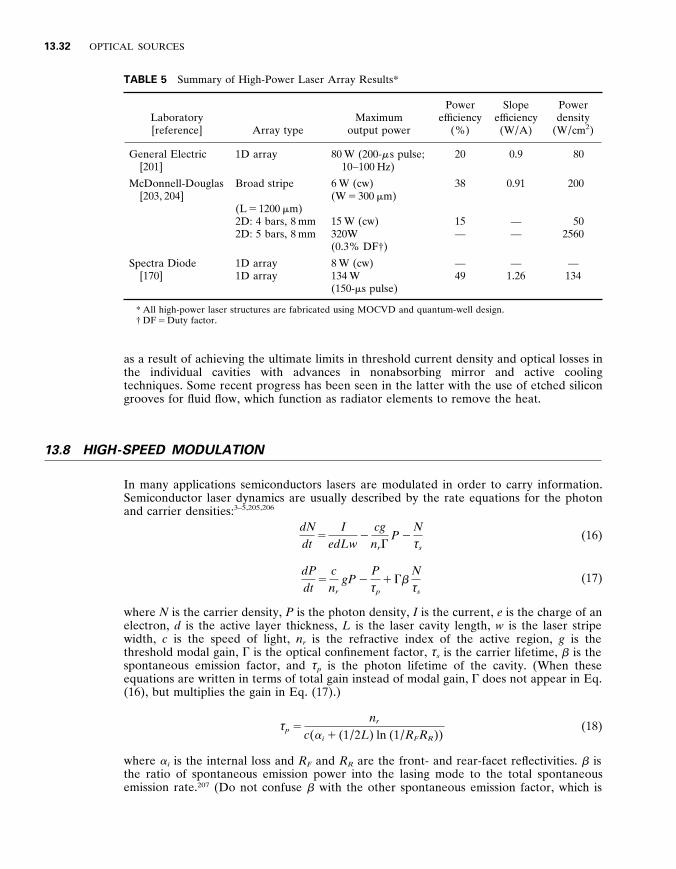
13 .32 OPTICAL SOURCES
TABLE 5 Summary of High-Power Laser Array Results*
Laboratory [reference] Array type
Maximum output power
Power ef ficiency
(%)
Slope ef ficiency (W / A)
Power density
(W / cm 2 )
General Electric [201]
1D array 80 W (200- m s pulse ; 10 – 100 Hz)
20 0 . 9 80
McDonnell-Douglas [203 , 204]
Broad stripe 6 W (cw) (W 5 300 m m)
38 0 . 91 200
(L 5 1200 m m) 2D : 4 bars , 8 mm 2D : 5 bars , 8 mm
15 W (cw) 320W (0 . 3% DF † )
15 —
— —
50 2560
Spectra Diode [170]
1D array 1D array
8 W (cw) 134 W (150- m s pulse)
— 49
— 1 . 26
— 134
* All high-power laser structures are fabricated using MOCVD and quantum-well design . † DF 5 Duty factor .
as a result of achieving the ultimate limits in threshold current density and optical losses in the individual cavities with advances in nonabsorbing mirror and active cooling techniques . Some recent progress has been seen in the latter with the use of etched silicon grooves for fluid flow , which function as radiator elements to remove the heat .
1 3 . 8 HIGH - SPEED MODULATION
In many applications semiconductors lasers are modulated in order to carry information . Semiconductor laser dynamics are usually described by the rate equations for the photon and carrier densities : 3–5 , 205 , 206
dN dt
5 I
edLw 2
cg n r G
P 2 N τ s
(16)
dP dt
5 c n r
gP 2 P τ p
1 G b N τ s
(17)
where N is the carrier density , P is the photon density , I is the current , e is the charge of an electron , d is the active layer thickness , L is the laser cavity length , w is the laser stripe width , c is the speed of light , n r is the refractive index of the active region , g is the threshold modal gain , G is the optical confinement factor , τ s is the carrier lifetime , b is the spontaneous emission factor , and τ p is the photon lifetime of the cavity . (When these equations are written in terms of total gain instead of modal gain , G does not appear in Eq . (16) , but multiplies the gain in Eq . (17) . )
τ p 5 n r
c ( a i 1 (1 / 2 L ) ln (1 / R F R R )) (18)
where a i is the internal loss and R F and R R are the front- and rear-facet reflectivities . b is the ratio of spontaneous emission power into the lasing mode to the total spontaneous emission rate . 2 0 7 (Do not confuse b with the other spontaneous emission factor , which is
SEMICONDUCTOR LASERS 13 .33
FIGURE 18 Schematic diagram of the two-dimensional rack-stack laser array architecture . ( Courtesy of R . Solarz , Lawrence Li y ermore . )
used in linewidth theory and is defined as the ratio of the spontaneous emission power into the lasing mode to the stimulated emission power of the mode . )
When a semiconductor laser is modulated there is some delay before it reaches a steady state . Because it takes time for a carrier population to build up , there will be a time delay τ d before the final photon density P o n is reached (see Fig . 19) . Once P o n is reached , additional time is required for the carrier and photon populations to come into equilibrium . The output power therefore goes through relaxation oscillations before finally reaching a steady state . This type of oscillation has many parallels in other second-order systems , 2 0 8 such as the vibration of a damped spring or an RLC circuit .
The frequency of these relaxation oscillations , f r is called the relaxation , resonance , or corner frequency . By considering small deviations from the steady state where N 5 N t h 1 D N and P 5 P o n 1 D P , we can solve Eqs . (16) and (17) for f r with the result : 5 , 205
f r > 1
2 π – c n r G
dg dN
P o n
τ p 5
1 2 π – c
n r
dg dN
( I 2 I t h ) edLw
(19)
where dg / dN is the dif ferential modal gain . For bulk double-heterostructure lasers the gain is linearly dependent on the carrier density and ( c / n r ) dg / dN is replaced by A , where A is a constant . As discussed earlier in the chapter , the gain-versus-carrier-density relationship of a quantum well is nonlinear , so A is not a constant for a QW laser .
Let us return our attention to the turn on delay τ d between a current increase and the beginning of relaxation oscillations as illustrated in Fig . 19 . If the initial current I of f is below I t h , the initial photon density P of f can be neglected in Eq . (16) . Assuming an exponential increase in carrier density we can derive 2 0 6
τ d 5 τ s ln S I o n 2 I of f
I o n 2 I t h D , I of f , I t h , I o n (20)
Since τ s is on the order of several ns , τ d is usually very large for semiconductor lasers with I of f below I t h . For example , with τ s 5 4 ns , I o n 5 20 mA , I t h 5 10 mA , and I of f 5 5 mA , τ d will be 1 . 6 ns . If a short current pulse is applied to a laser biased below threshold , τ d may be so long that the laser barely responds (see Fig . 20) . When a current pulse ends , it takes
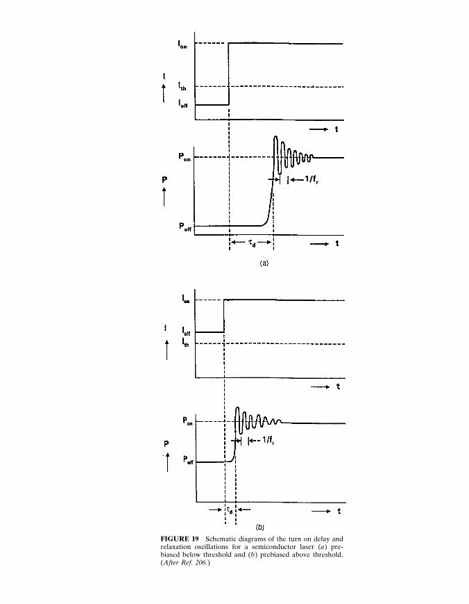
FIGURE 19 Schematic diagrams of the turn on delay and relaxation oscillations for a semiconductor laser ( a ) pre- biased below threshold and ( b ) prebiased above threshold . ( After Ref . 2 0 6 . )
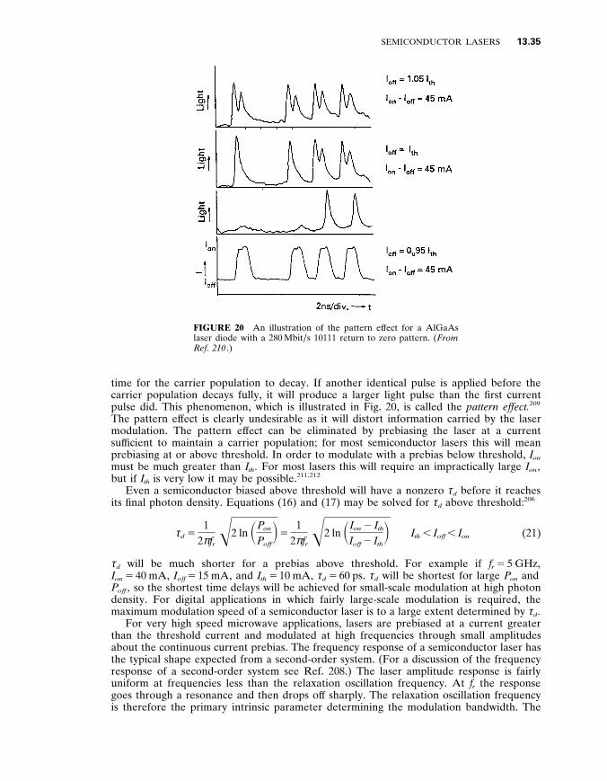
SEMICONDUCTOR LASERS 13 .35
FIGURE 20 An illustration of the pattern ef fect for a AlGaAs laser diode with a 280 Mbit / s 10111 return to zero pattern . ( From Ref . 2 1 0 . )
time for the carrier population to decay . If another identical pulse is applied before the carrier population decays fully , it will produce a larger light pulse than the first current pulse did . This phenomenon , which is illustrated in Fig . 20 , is called the pattern ef fect . 2 0 9
The pattern ef fect is clearly undesirable as it will distort information carried by the laser modulation . The pattern ef fect can be eliminated by prebiasing the laser at a current suf ficient to maintain a carrier population ; for most semiconductor lasers this will mean prebiasing at or above threshold . In order to modulate with a prebias below threshold , I o n must be much greater than I t h . For most lasers this will require an impractically large I o n , but if I t h is very low it may be possible . 211 , 212
Even a semiconductor biased above threshold will have a nonzero τ d before it reaches its final photon density . Equations (16) and (17) may be solved for τ d above threshold : 206
τ d 5 1
2 π f r – 2 ln S P o n
P of f D 5
1 2 π f r
– 2 ln S I o n 2 I t h
I of f 2 I t h D I t h , I of f , I o n (21)
τ d will be much shorter for a prebias above threshold . For example if f r 5 5 GHz , I o n 5 40 mA , I of f 5 15 mA , and I t h 5 10 mA , τ d 5 60 ps . τ d will be shortest for large P o n and P of f , so the shortest time delays will be achieved for small-scale modulation at high photon density . For digital applications in which fairly large-scale modulation is required , the maximum modulation speed of a semiconductor laser is to a large extent determined by τ d .
For very high speed microwave applications , lasers are prebiased at a current greater than the threshold current and modulated at high frequencies through small amplitudes about the continuous current prebias . The frequency response of a semiconductor laser has the typical shape expected from a second-order system . (For a discussion of the frequency response of a second-order system see Ref . 208 . ) The laser amplitude response is fairly uniform at frequencies less than the relaxation oscillation frequency . At f r the response goes through a resonance and then drops of f sharply . The relaxation oscillation frequency is therefore the primary intrinsic parameter determining the modulation bandwidth . The
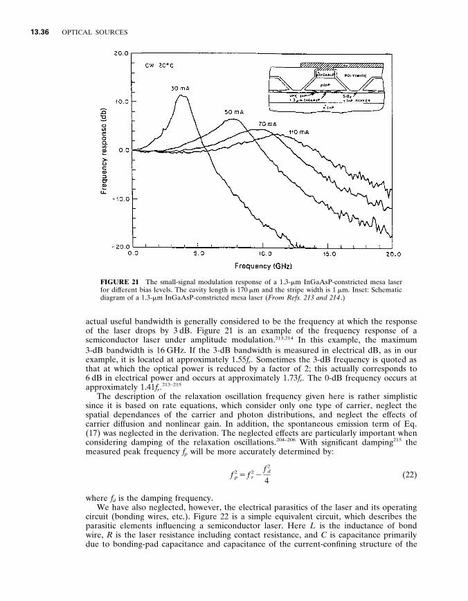
13 .36 OPTICAL SOURCES
FIGURE 21 The small-signal modulation response of a 1 . 3- m m InGaAsP-constricted mesa laser for dif ferent bias levels . The cavity length is 170 m m and the stripe width is 1 m m . Inset : Schematic diagram of a 1 . 3- m m InGaAsP-constricted mesa laser ( From Refs . 2 1 3 and 2 1 4 . )
actual useful bandwidth is generally considered to be the frequency at which the response of the laser drops by 3 dB . Figure 21 is an example of the frequency response of a semiconductor laser under amplitude modulation . 213 , 214 In this example , the maximum 3-dB bandwidth is 16 GHz . If the 3-dB bandwidth is measured in electrical dB , as in our example , it is located at approximately 1 . 55 f r . Sometimes the 3-dB frequency is quoted as that at which the optical power is reduced by a factor of 2 ; this actually corresponds to 6 dB in electrical power and occurs at approximately 1 . 73 f r . The 0-dB frequency occurs at approximately 1 . 41 f r .
213–215
The description of the relaxation oscillation frequency given here is rather simplistic since it is based on rate equations , which consider only one type of carrier , neglect the spatial dependances of the carrier and photon distributions , and neglect the ef fects of carrier dif fusion and nonlinear gain . In addition , the spontaneous emission term of Eq . (17) was neglected in the derivation . The neglected ef fects are particularly important when considering damping of the relaxation oscillations . 204–206 With significant damping 2 1 5 the measured peak frequency f p will be more accurately determined by :
f 2 p 5 f 2
r 2 f 2
d
4 (22)
where f d is the damping frequency . We have also neglected , however , the electrical parasitics of the laser and its operating
circuit (bonding wires , etc . ) . Figure 22 is a simple equivalent circuit , which describes the parasitic elements influencing a semiconductor laser . Here L is the inductance of bond wire , R is the laser resistance including contact resistance , and C is capacitance primarily due to bonding-pad capacitance and capacitance of the current-confining structure of the
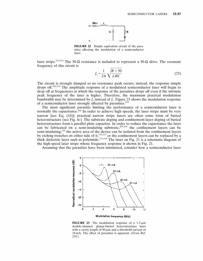
SEMICONDUCTOR LASERS 13 .37
FIGURE 22 Simple equivalent circuit of the para- sitics af fecting the modulation of a semiconductor laser .
laser stripe . 213 , 214 The 50- Ω resistance is included to represent a 50- Ω drive . The resonant frequency of this circuit is
f o 5 1
2 π – R 1 50 LRC
(23)
The circuit is strongly damped so no resonance peak occurs ; instead , the response simply drops of f . 205 , 218 The amplitude response of a modulated semiconductor laser will begin to drop of f at frequencies at which the response of the parasitics drops of f even if the intrinsic peak frequency of the laser is higher . Therefore , the maximum practical modulation bandwidth may be determined by f o instead of f r . Figure 23 shows the modulation response of a semiconductor laser strongly af fected by parasitics . 2 1 9
The most significant parasitic limiting the performance of a semiconductor laser is normally the capacitance . 2 0 5 In order to achieve high speeds , the laser stripe must be very narrow [see Eq . (18)] ; practical narrow stripe lasers are often some form of buried heterostructure (see Fig . 4 c ) . The substrate doping and confinement-layer doping of buried heterostructure form a parallel plate capacitor . In order to reduce the capacitance the laser can be fabricated on a semi-insulating substrate , 205 , 218 the confinement layers can be semi-insulating , 1 2 4 the active area of the device can be isolated from the confinement layers by etching trenches on either side of it , 124 , 125 or the confinement layers can be replaced by a thick dielectric layer such as polyimide . 213 , 214 The inset on Fig . 21 is a schematic diagram of the high-speed laser stripe whose frequency response is shown in Fig . 21 .
Assuming that the parasitics have been minimized , consider how a semiconductor laser
FIGURE 23 The modulation response of a 1 . 3- m m double-channel , planar-buried heterostructure laser with a cavity length of 80 m m and a threshold current of 18 mA . The ef fect of parasitics is apparent . ( From Ref . 2 1 9 . )
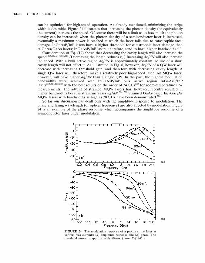
13 .38 OPTICAL SOURCES
can be optimized for high-speed operation . As already mentioned , minimizing the stripe width is desirable . Figure 21 illustrates that increasing the photon density (or equivalently the current) increases the speed . Of course there will be a limit as to how much the photon density can be increased ; when the photon density of a semiconductor laser is increased , eventually a maximum power is reached at which the laser fails due to catastrophic facet damage . InGaAsP / InP lasers have a higher threshold for catastrophic facet damage than AlGaAs / GaAs lasers ; InGaAsP / InP lasers , therefore , tend to have higher bandwidths . 2 1 4
Consideration of Eq . (19) shows that decreasing the cavity length will also increase the speed . 205 , 213 , 214 , 218 , 219 (Decreasing the length reduces τ p . ) Increasing dg / dN will also increase the speed . With a bulk active region dg / dN is approximately constant , so use of a short cavity length will not af fect it . As illustrated in Fig . 6 , however , dg / dN of a QW laser will decrease with increasing threshold gain , and therefore with decreasing cavity length . A single QW laser will , therefore , make a relatively poor high-speed laser . An MQW laser , however , will have higher dg / dN than a single QW . In the past , the highest modulation bandwidths were achieved with InGaAsP / InP bulk active region InGaAsP / InP lasers 213 , 214 , 222 , 223 with the best results on the order of 24 GHz 2 2 3 for room-temperature CW measurements . The advent of strained MQW lasers has , however , recently resulted in higher bandwidths because strain increases dg / dN . 224–226 Strained GaAs-based In 0 . 3 Ga 0 . 7 As MQW lasers with bandwidths as high as 28 GHz have been demonstrated . 2 2 6
So far our discussion has dealt only with the amplitude response to modulation . The phase and lasing wavelength (or optical frequency) are also af fected by modulation . Figure 24 is an example of the phase response which accompanies the amplitude response of a semiconductor laser under modulation .
(a)
(b)
FIGURE 24 The modulation response of a proton stripe laser at various bias currents : ( a ) amplitude response and ( b ) phase . The threshold current is approximately 80 mA . ( From Ref . 2 0 5 . )
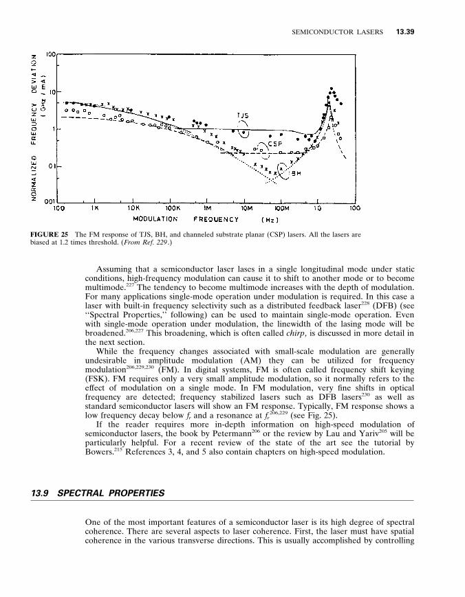
SEMICONDUCTOR LASERS 13 .39
FIGURE 25 The FM response of TJS , BH , and channeled substrate planar (CSP) lasers . All the lasers are biased at 1 . 2 times threshold . ( From Ref . 2 2 9 . )
Assuming that a semiconductor laser lases in a single longitudinal mode under static conditions , high-frequency modulation can cause it to shift to another mode or to become multimode . 2 2 7 The tendency to become multimode increases with the depth of modulation . For many applications single-mode operation under modulation is required . In this case a laser with built-in frequency selectivity such as a distributed feedback laser 2 2 8 (DFB) (see ‘‘Spectral Properties , ’’ following) can be used to maintain single-mode operation . Even with single-mode operation under modulation , the linewidth of the lasing mode will be broadened . 206 , 227 This broadening , which is often called chirp , is discussed in more detail in the next section .
While the frequency changes associated with small-scale modulation are generally undesirable in amplitude modulation (AM) they can be utilized for frequency modulation 206 , 229 , 230 (FM) . In digital systems , FM is often called frequency shift keying (FSK) . FM requires only a very small amplitude modulation , so it normally refers to the ef fect of modulation on a single mode . In FM modulation , very fine shifts in optical frequency are detected ; frequency stabilized lasers such as DFB lasers 2 3 0 as well as standard semiconductor lasers will show an FM response . Typically , FM response shows a low frequency decay below f r and a resonance at f r
206 , 229 (see Fig . 25) . If the reader requires more in-depth information on high-speed modulation of
semiconductor lasers , the book by Petermann 2 0 6 or the review by Lau and Yariv 2 0 5 will be particularly helpful . For a recent review of the state of the art see the tutorial by Bowers . 2 1 5 References 3 , 4 , and 5 also contain chapters on high-speed modulation .
1 3 . 9 SPECTRAL PROPERTIES
One of the most important features of a semiconductor laser is its high degree of spectral coherence . There are several aspects to laser coherence . First , the laser must have spatial coherence in the various transverse directions . This is usually accomplished by controlling
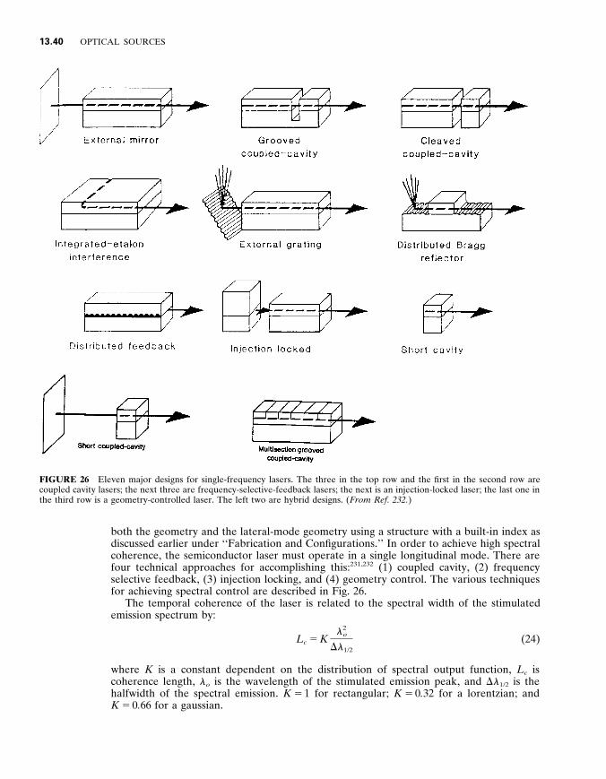
13 .40 OPTICAL SOURCES
FIGURE 26 Eleven major designs for single-frequency lasers . The three in the top row and the first in the second row are coupled cavity lasers ; the next three are frequency-selective-feedback lasers ; the next is an injection-locked laser ; the last one in the third row is a geometry-controlled laser . The left two are hybrid designs . ( From Ref . 2 3 2 . )
both the geometry and the lateral-mode geometry using a structure with a built-in index as discussed earlier under ‘‘Fabrication and Configurations . ’’ In order to achieve high spectral coherence , the semiconductor laser must operate in a single longitudinal mode . There are four technical approaches for accomplishing this : 231 , 232 (1) coupled cavity , (2) frequency selective feedback , (3) injection locking , and (4) geometry control . The various techniques for achieving spectral control are described in Fig . 26 .
The temporal coherence of the laser is related to the spectral width of the stimulated emission spectrum by :
L c 5 K l 2
o
D l 1/2
(24)
where K is a constant dependent on the distribution of spectral output function , L c is coherence length , l o is the wavelength of the stimulated emission peak , and D l 1/2 is the halfwidth of the spectral emission . K 5 1 for rectangular ; K 5 0 . 32 for a lorentzian ; and K 5 0 . 66 for a gaussian .
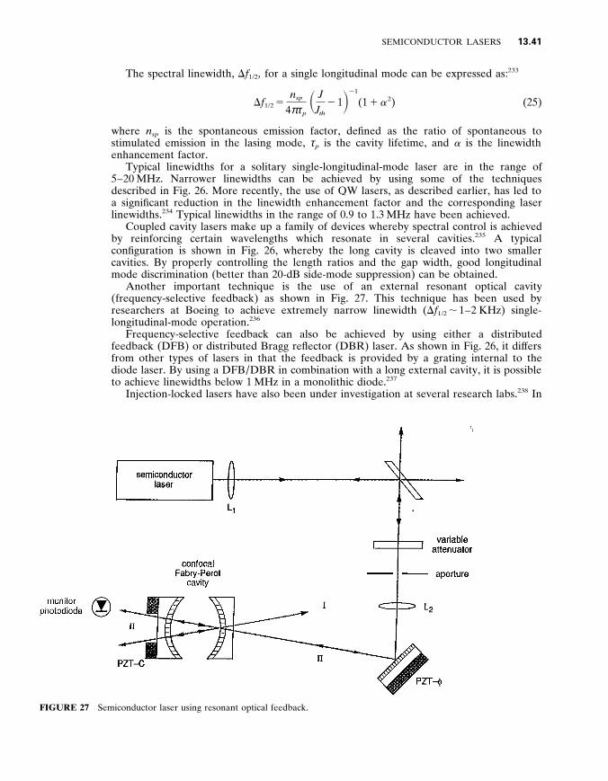
SEMICONDUCTOR LASERS 13 .41
The spectral linewidth , D f 1/2 , for a single longitudinal mode can be expressed as : 2 3 3
D f 1/2 5 n s p
4 π τ p S J
J t h 2 1 D 2 1
(1 1 a 2 ) (25)
where n s p is the spontaneous emission factor , defined as the ratio of spontaneous to stimulated emission in the lasing mode , τ p is the cavity lifetime , and a is the linewidth enhancement factor .
Typical linewidths for a solitary single-longitudinal-mode laser are in the range of 5 – 20 MHz . Narrower linewidths can be achieved by using some of the techniques described in Fig . 26 . More recently , the use of QW lasers , as described earlier , has led to a significant reduction in the linewidth enhancement factor and the corresponding laser linewidths . 2 3 4 Typical linewidths in the range of 0 . 9 to 1 . 3 MHz have been achieved .
Coupled cavity lasers make up a family of devices whereby spectral control is achieved by reinforcing certain wavelengths which resonate in several cavities . 2 3 5 A typical configuration is shown in Fig . 26 , whereby the long cavity is cleaved into two smaller cavities . By properly controlling the length ratios and the gap width , good longitudinal mode discrimination (better than 20-dB side-mode suppression) can be obtained .
Another important technique is the use of an external resonant optical cavity (frequency-selective feedback) as shown in Fig . 27 . This technique has been used by researchers at Boeing to achieve extremely narrow linewidth ( D f 1/2 , 1 – 2 KHz) single- longitudinal-mode operation . 2 3 6
Frequency-selective feedback can also be achieved by using either a distributed feedback (DFB) or distributed Bragg reflector (DBR) laser . As shown in Fig . 26 , it dif fers from other types of lasers in that the feedback is provided by a grating internal to the diode laser . By using a DFB / DBR in combination with a long external cavity , it is possible to achieve linewidths below 1 MHz in a monolithic diode . 2 3 7
Injection-locked lasers have also been under investigation at several research labs . 2 3 8 In
FIGURE 27 Semiconductor laser using resonant optical feedback .
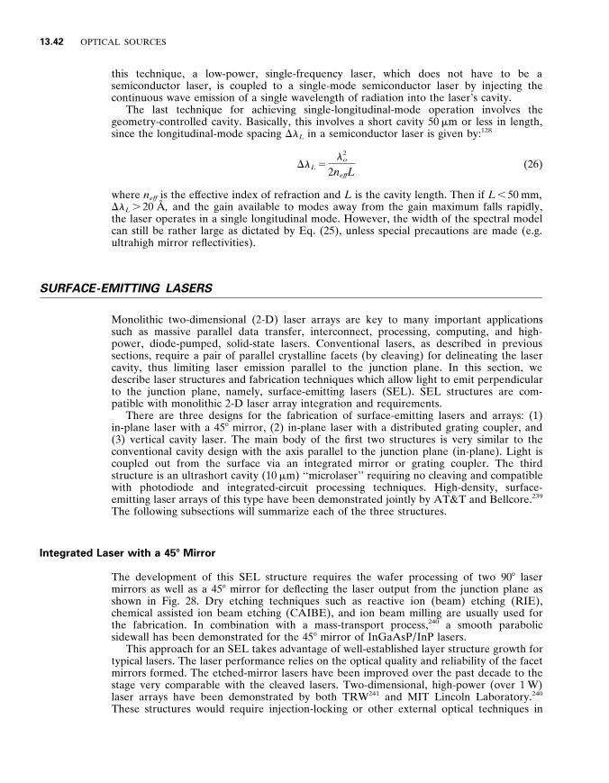
13 .42 OPTICAL SOURCES
this technique , a low-power , single-frequency laser , which does not have to be a semiconductor laser , is coupled to a single-mode semiconductor laser by injecting the continuous wave emission of a single wavelength of radiation into the laser’s cavity .
The last technique for achieving single-longitudinal-mode operation involves the geometry-controlled cavity . Basically , this involves a short cavity 50 m m or less in length , since the longitudinal-mode spacing D l L in a semiconductor laser is given by : 1 2 8
D l L 5 l 2
o
2 n ef f L (26)
where n ef f is the ef fective index of refraction and L is the cavity length . Then if L , 50 mm , D l L . 20 Å , and the gain available to modes away from the gain maximum falls rapidly , the laser operates in a single longitudinal mode . However , the width of the spectral model can still be rather large as dictated by Eq . (25) , unless special precautions are made (e . g . ultrahigh mirror reflectivities) .
SURFACE - EMITTING LASERS
Monolithic two-dimensional (2-D) laser arrays are key to many important applications such as massive parallel data transfer , interconnect , processing , computing , and high- power , diode-pumped , solid-state lasers . Conventional lasers , as described in previous sections , require a pair of parallel crystalline facets (by cleaving) for delineating the laser cavity , thus limiting laser emission parallel to the junction plane . In this section , we describe laser structures and fabrication techniques which allow light to emit perpendicular to the junction plane , namely , surface-emitting lasers (SEL) . SEL structures are com- patible with monolithic 2-D laser array integration and requirements .
There are three designs for the fabrication of surface-emitting lasers and arrays : (1) in-plane laser with a 45 8 mirror , (2) in-plane laser with a distributed grating coupler , and (3) vertical cavity laser . The main body of the first two structures is very similar to the conventional cavity design with the axis parallel to the junction plane (in-plane) . Light is coupled out from the surface via an integrated mirror or grating coupler . The third structure is an ultrashort cavity (10 m m) ‘‘microlaser’’ requiring no cleaving and compatible with photodiode and integrated-circuit processing techniques . High-density , surface- emitting laser arrays of this type have been demonstrated jointly by AT&T and Bellcore . 2 3 9
The following subsections will summarize each of the three structures .
Integrated Laser with a 45 8 Mirror
The development of this SEL structure requires the wafer processing of two 90 8 laser mirrors as well as a 45 8 mirror for deflecting the laser output from the junction plane as shown in Fig . 28 . Dry etching techniques such as reactive ion (beam) etching (RIE) , chemical assisted ion beam etching (CAIBE) , and ion beam milling are usually used for the fabrication . In combination with a mass-transport process , 2 4 0 a smooth parabolic sidewall has been demonstrated for the 45 8 mirror of InGaAsP / InP lasers .
This approach for an SEL takes advantage of well-established layer structure growth for typical lasers . The laser performance relies on the optical quality and reliability of the facet mirrors formed . The etched-mirror lasers have been improved over the past decade to the stage very comparable with the cleaved lasers . Two-dimensional , high-power (over 1 W) laser arrays have been demonstrated by both TRW 2 4 1 and MIT Lincoln Laboratory . 2 4 0
These structures would require injection-locking or other external optical techniques in
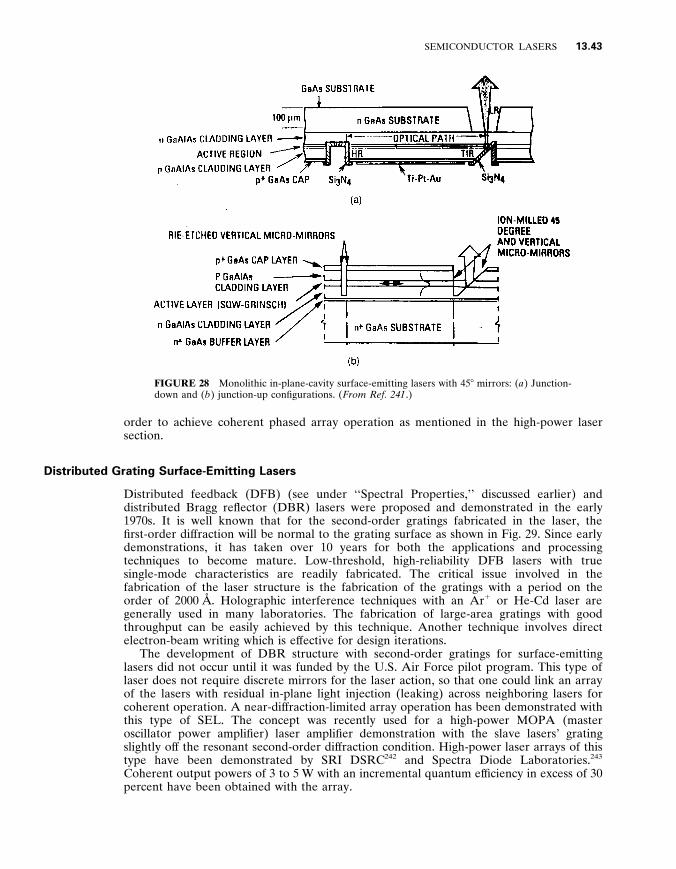
SEMICONDUCTOR LASERS 13 .43
FIGURE 28 Monolithic in-plane-cavity surface-emitting lasers with 45 8 mirrors : ( a ) Junction- down and ( b ) junction-up configurations . ( From Ref . 2 4 1 . )
order to achieve coherent phased array operation as mentioned in the high-power laser section .
Distributed Grating Surface-Emitting Lasers
Distributed feedback (DFB) (see under ‘‘Spectral Properties , ’’ discussed earlier) and distributed Bragg reflector (DBR) lasers were proposed and demonstrated in the early 1970s . It is well known that for the second-order gratings fabricated in the laser , the first-order dif fraction will be normal to the grating surface as shown in Fig . 29 . Since early demonstrations , it has taken over 10 years for both the applications and processing techniques to become mature . Low-threshold , high-reliability DFB lasers with true single-mode characteristics are readily fabricated . The critical issue involved in the fabrication of the laser structure is the fabrication of the gratings with a period on the order of 2000 Å . Holographic interference techniques with an Ar 1 or He-Cd laser are generally used in many laboratories . The fabrication of large-area gratings with good throughput can be easily achieved by this technique . Another technique involves direct electron-beam writing which is ef fective for design iterations .
The development of DBR structure with second-order gratings for surface-emitting lasers did not occur until it was funded by the U . S . Air Force pilot program . This type of laser does not require discrete mirrors for the laser action , so that one could link an array of the lasers with residual in-plane light injection (leaking) across neighboring lasers for coherent operation . A near-dif fraction-limited array operation has been demonstrated with this type of SEL . The concept was recently used for a high-power MOPA (master oscillator power amplifier) laser amplifier demonstration with the slave lasers’ grating slightly of f the resonant second-order dif fraction condition . High-power laser arrays of this type have been demonstrated by SRI DSRC 2 4 2 and Spectra Diode Laboratories . 2 4 3
Coherent output powers of 3 to 5 W with an incremental quantum ef ficiency in excess of 30 percent have been obtained with the array .
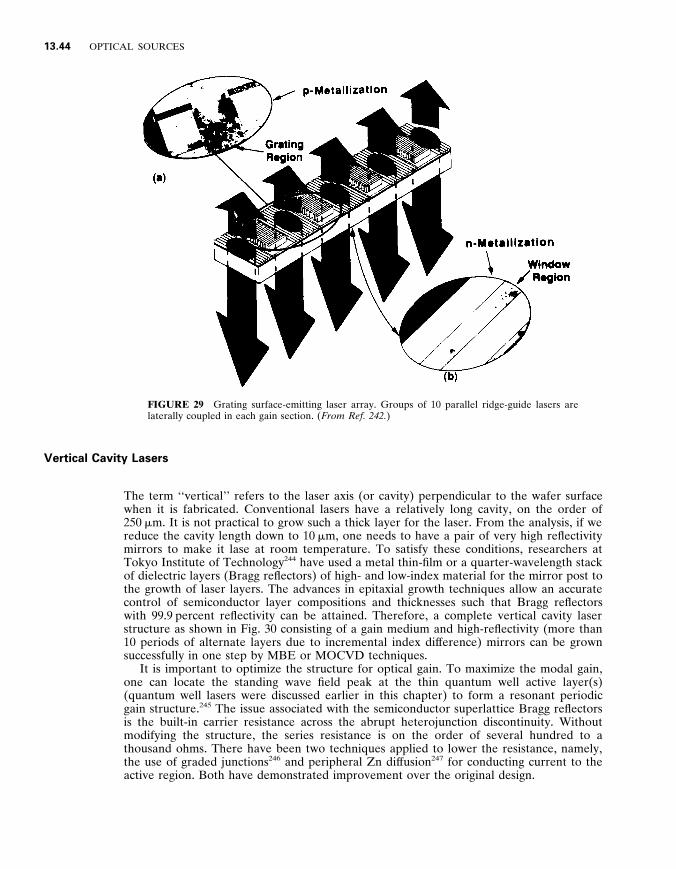
13 .44 OPTICAL SOURCES
FIGURE 29 Grating surface-emitting laser array . Groups of 10 parallel ridge-guide lasers are laterally coupled in each gain section . ( From Ref . 2 4 2 . )
Vertical Cavity Lasers
The term ‘‘vertical’’ refers to the laser axis (or cavity) perpendicular to the wafer surface when it is fabricated . Conventional lasers have a relatively long cavity , on the order of 250 m m . It is not practical to grow such a thick layer for the laser . From the analysis , if we reduce the cavity length down to 10 m m , one needs to have a pair of very high reflectivity mirrors to make it lase at room temperature . To satisfy these conditions , researchers at Tokyo Institute of Technology 2 4 4 have used a metal thin-film or a quarter-wavelength stack of dielectric layers (Bragg reflectors) of high- and low-index material for the mirror post to the growth of laser layers . The advances in epitaxial growth techniques allow an accurate control of semiconductor layer compositions and thicknesses such that Bragg reflectors with 99 . 9 percent reflectivity can be attained . Therefore , a complete vertical cavity laser structure as shown in Fig . 30 consisting of a gain medium and high-reflectivity (more than 10 periods of alternate layers due to incremental index dif ference) mirrors can be grown successfully in one step by MBE or MOCVD techniques .
It is important to optimize the structure for optical gain . To maximize the modal gain , one can locate the standing wave field peak at the thin quantum well active layer(s) (quantum well lasers were discussed earlier in this chapter) to form a resonant periodic gain structure . 2 4 5 The issue associated with the semiconductor superlattice Bragg reflectors is the built-in carrier resistance across the abrupt heterojunction discontinuity . Without modifying the structure , the series resistance is on the order of several hundred to a thousand ohms . There have been two techniques applied to lower the resistance , namely , the use of graded junctions 2 4 6 and peripheral Zn dif fusion 2 4 7 for conducting current to the active region . Both have demonstrated improvement over the original design .
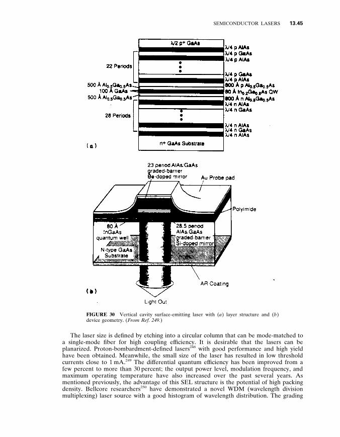
SEMICONDUCTOR LASERS 13 .45
FIGURE 30 Vertical cavity surface-emitting laser with ( a ) layer structure and ( b ) device geometry . ( From Ref . 2 4 9 . )
The laser size is defined by etching into a circular column that can be mode-matched to a single-mode fiber for high coupling ef ficiency . It is desirable that the lasers can be planarized . Proton-bombardment-defined lasers 2 4 8 with good performance and high yield have been obtained . Meanwhile , the small size of the laser has resulted in low threshold currents close to 1 mA . 2 4 9 The dif ferential quantum ef ficiency has been improved from a few percent to more than 30 percent ; the output power level , modulation frequency , and maximum operating temperature have also increased over the past several years . As mentioned previously , the advantage of this SEL structure is the potential of high packing density . Bellcore researchers 2 5 0 have demonstrated a novel WDM (wavelength division multiplexing) laser source with a good histogram of wavelength distribution . The grading
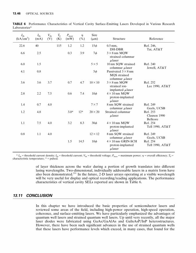
13 .46 OPTICAL SOURCES
TABLE 6 Performance Characteristics of Vertical Cavity Surface-Emitting Lasers Developed in Various Research Laboratories*
J t h (kA / cm 2 )
I t h (mA)
V t h (V)
T 0 (K)
P max
(mW) h
(%) Size ( m m) Structure Reference
22 . 6 40 115 1 . 2 1 . 2 15 f 0 . 5 mm , DH-DBR
Ref . 246 , Tai , AT&T
6 . 6 2 . 5 0 . 3 3 . 9 7 f 3 3 8 nm MQW strained columnar m laser
6 . 0 1 . 5 5 3 5 10 nm SQW strained columnar m laser
Ref . 240 Jewell , AT&T
4 . 1 0 . 8 5 f Passivated 3 3 8 nm MQS strained columnar m laser
3 . 6 3 . 6 3 . 7 0 . 7 4 . 7 10 3 10 3 3 8 nm MQW strained ion- implanted m laser
Ref . 252 Lee 1990 , AT&T
2 . 8 2 . 2 7 . 5 0 . 6 7 . 4 10 f 4 3 10 nm MQW proton-implanted m laser
1 . 4 0 . 7 4 . 0 7 3 7 8 nm SQW strained columnar m laser
Ref . 249 Geels , UCSB
1 . 2 4 . 8 3 . 0* 12* 20 3 20 Strained columnar m laser
Ref . 253 Clausen 1990 Bellcore
1 . 1 7 . 5 4 . 0 3 . 2 8 . 3 30 f 4 3 10 nm MQW proton-implanted m laser
Ref . 254 Tell 1990 , AT&T
0 . 8 1 . 1 4 . 0 12 3 12 8 nm SQW strained columnar m laser
Ref . 249 Geels , UCSB
1 . 5 14 . 5 10 f 4 3 10 nm GRIN-SCH proton-implanted m laser
Ref . 254 Tell 1990 , AT&T
* J t h 5 threshold current density ; I t h 5 threshold current ; V t h 5 threshold voltage ; P max 5 maximum power ; h 5 overall ef ficiency ; T 0 5 characteristic temperature ; * 5 pulsed .
of layer thickness across the wafer during a portion of growth translates into dif ferent lasing wavelengths . Two-dimensional , individually addressable lasers in a matrix form have also been demonstrated . 2 5 1 In the future , 2-D laser arrays operating at a visible wavelength will be very useful for display and optical recording / reading applications . The performance characteristics of vertical cavity SELs reported are shown in Table 6 .
1 3 . 1 1 CONCLUSION
In this chapter we have introduced the basic properties of semiconductor lasers and reviewed some areas of the field , including high-power operation , high-speed operation , coherence , and surface-emitting lasers . We have particularly emphasized the advantages of quantum well lasers and strained quantum well lasers . Up until very recently , all the major laser diodes were fabricated using GaAs / GaAlAs and GaInAsP / InP heterostructures . However , there have been such significant advances in the use of strained quantum wells that these lasers have performance levels which exceed , in many cases , that found for the
SEMICONDUCTOR LASERS 13 .47
unstrained lasers . Coupled with the measured excellent reliability results and better output power / temperature performance , these types of lasers will experience a high demand in the future . High-power strained InGaAs / GaAs quantum well lasers are also of interest because their lasing wavelength range includes 0 . 98 m m , which makes them useful for pumping erbium-doped fiber amplifiers . 1 7
Another trend in the future will be the extension of commercial semiconductor lasers to a wider variety of lasing wavelengths . Just as with the standard lasers , strained quantum wells result in significant performance improvements in these more novel laser systems . Shorter wavelength ( l , 0 . 75 m m) lasers with high output powers are of interest for high-density optical recording and printing . In the last few years , much progress has been made in developing short wavelength semiconductor lasers . In the near future , practical visible wavelength lasers will be in the red-to-yellow range , but progress has begun on even shorter wavelengths in the blue . Recent work on very long wavelength ( l . 2 . 0 m m) GaInAsSb / AlGaAsSb lasers is also very promising . Long wavelengths ( . 1 . 55 m m) are of interest for eye-safe laser radar , metrology , and medical instrumentation .
Currently , commercial lasers are of the edge-emitting variety , but two-dimensional surface-emitting laser arrays have advanced considerably in the past few years . When they reach maturity , they will be used for pixel interconnect and display applications .
In a limited chapter such as this it is impossible to cover all areas of the field of semiconductor lasers in depth . One of the most important areas neglected is that of tunable lasers . 255–257 Single-mode tunable DFB and DBR lasers are of great interest for future coherent optical transmission systems . These lasers lase in a single longitudinal mode , but that mode can be tuned to a range of frequencies .
Another area not discussed in detail here is amplifiers . Amplifiers are of great interest for long-haul communication systems , for example , submarine cable systems . Amplifiers can be laser pumped fiber amplifiers 1 7 or laser amplifiers . 258–262 A laser amplifier has a structure similar to that of a semiconductor laser and has some optical gain , but only enough to amplify an existing signal , not enough to lase on its own .
It is hoped that the information presented in this chapter will satisfy readers who are interested in the basics of the subject and will give readers interested in greater depth the understanding necessary to probe further in order to satisfy their specific requirements .
1 3 . 1 2 REFERENCES
1 . H . C . Casey , Jr ., and M . B . Panish , Heterostructure Lasers , Part A : Fundamental Principles , Academic Press , Orlando , 1978 .
2 . H . C . Casey , Jr ., and M . B . Panish , Heterostructure Lasers , Part B : Materials and Operating Characteristics , Academic Press , Orlando , 1978 .
3 . G . H . B . Thompson , Physics of Semiconductor Laser De y ices , John Wiley & Sons , New York , 1980 .
4 . G . P . Agrawal and N . K . Dutta , Long - Wa y elength Semiconductor Lasers , Van Nostrand Reinhold , New York , 1986 .
5 . H . Kressel and J . K . Butler , Semiconductor Lasers and Heterojuction LEDs , Academic Press , New York , 1977 .
6 . R . A . Bartolini , A . E . Bell , and F . W . Spong , IEEE J . Quantum Electron . QE-17 : 69 (1981) . 7 . R . N . Bhargava , J . Cryst . Growth 117 : 894 (1992) . 8 . C . Lin (ed . ) , Optoelectronic Technology and Lightwa y e Communication Systems , Van Nostrand ,
Reinhold , New York , 1989 . 9 . S . E . Miller and I . Kaminow (eds . ) , Optical Fiber Telecomunications , Academic Press , Orlando ,
1988 . 10 . M . Katzman (ed . ) , Laser Satellite Communications , Prentice-Hall , Englewood Clif fs , N . J ., 1987 .
13 .48 OPTICAL SOURCES
11 . M . Ross , Proc . SPIE 885 : 2 (1988) . 12 . J . D . McClure , Proc . SPIE 1219 : 446 (1990) . 13 . G . Abbas , W . R . Babbitt , M . de La Chappelle , M . L . Fleshner , and J . D . McClure , Proc . SPIE
1219 : 468 (1990) . 14 . J . W . Goodman , International Trends in Optica , Academic Press , Orlando , 1991 . 15 . R . Olshansky , V . Lanzisera , and P . Hill , J . Lightwa y e Technology 7 : 1329 (1989) . 16 . R . L . Byer , Proc . of the CLEO / IQEC Conf . , Plenary Session , Baltimore , Md ., 1987 . 17 . K . Nakagawa , S . Nishi , K . Aida , and E . Yonoda , J . Lightwa y e Technology 9 : 198 (1991) . 18 . T . F . Deutch , J . Boll , C . A . Poliafito , K . To , Proc . of the CLEO Conf . , San Francisco , Calif .,
1986 . 19 . C . Kittel , Introduction to Solid State Physics , John Wiley & Sons , New York , 1976 . 20 . L . Figueroa , ‘‘Semiconductor Lasers , ’’ Handbook of Microwa y e and Optical Components , K .
Chang (ed . ) , J . Wiley & Sons , New York , 1990 . 21 . R . N . Hall , G . E . Fenner , J . D . Kingsley , T . J . Soltys , and R . O . Carlson , Phys . Re y . Lett . 9 : 366
(1962) . 22 . M . I . Nathan , W . P . Dumke , G . Burns , F . H . Dill , Jr ., and G . Lasher , Appl . Phys . Lett . 1 : 62
(1962) . 23 . N . Holonyak , Jr . and S . F . Bevacqua , Appl . Phys . Lett . 1 : 82 (1962) . 24 . T . M . Quist , R . H . Rediker , R . J . Keyes , W . E . Krag , B . Lax , A . L . McWhorter , and H . J .
Zeigler , Appl . Phys . Lett . 1 : 91 (1962) . 25 . T . R . Chen , Y . Zhuang , Y . J . Xu , P . Derry , N . Bar-Chaim , A . Yariv , B . Yu , Q . Z . Wang , and
Y . Q . Zhou , Optics & Laser Tech . 22 : 245 (1990) . 26 . G . L . Bona , P . Buchmann , R . Clauberg , H . Jaeckel , P . Vettiger , O . Voegeli , and D . J . Webb ,
IEEE Photon . Tech . Lett . 3 : 412 (1991) . 27 . A Behfar-Rad , S . S . Wong , J . M . Ballantyne , B . A . Stolz , and C . M . Harding , Appl . Phys . Lett .
54 : 493 (1989) . 28 . N . Bouadma , J . F . Hogrel , J . Charil , and M . Carre , IEEE J . Quantum Electron . QE-23 : 909
(1987) . 29 . M . B . Panish , J . Sumski , and I . Hayashi , Met . Trans . 2 : 795 (1971) . 30 . W . T . Tsang (ed . ) , Semiconductors and Semimetals , vol . 22 , part A , Academic Press , New York ,
1971 , pp . 95 – 207 . 31 . R . D . Dupuis and P . D . Dapkus , IEEE J . Quantum Electron . QE-15 : 128 (1979) . 32 . R . D . Burnham , W . Streifer , T . L . Paoli , and N . Holonyak , Jr ., J . Cryst . Growth 68 : 370 (1984) . 33 . A . Y . Cho , Thin Solid Films 100 : 291 (1983) . 34 . K . Ploog , Crystal Growth , Properties and Applications , vol . 3 , H . C . Freyhardt (ed . ) ,
Springer-Verlag , Berlin , 1980 , pp . 73 – 162 . 35 . B . A . Joyce , Rep . Prog . Phys . 48 : 1637 (1985) . 36 . W . T . Tsang , J . Cryst . Growth 105 : 1 (1990) . 37 . W . T . Tsang , J . Cryst . Growth 95 : 121 (1989) . 38 . T . Hayakawa , T . Suyama , K . Takahashi , M . Kondo , S . Yamamoto , and T . Hijikata , Appl . Phys .
Lett . 51 : 707 (1987) . 39 . A . Kasukawa , R . Bhat , C . E . Zah , S . A . Schwarz , D . M . Hwang , M . A . Koza , and T . P . Lee ,
Electron . Lett . 27 : 1063 (1991) . 40 . J . I . Davies , A . C . Marchall , P . J . Williams , M . D . Scott , and A . C . Carter , Electron . Lett . 24 : 732
(1988) . 41 . W . T . Tsang and N . A . Olsson , Appl . Phys . Lett . 42 : 922 (1983) . 42 . H . Temkin , K . Alavi , W . R . Wagner , T . P . Pearsall , and A . Y . Cho , Appl . Phys . Lett . 42 : 845
(1983) . 43 . D . P . Bour , Proc . SPIE 1078 : 60 (1989) .
SEMICONDUCTOR LASERS 13 .49
44 . M . Ishikawa , K . Itaya , M . Okajima , and G . Hatakoshi , Proc . SPIE 1418 : 344 (1991) . 45 . G . Hatakoshi , K . Itaya , M . Ishikawa , M . Okajima , and Y . Uematsu , IEEE J . Quantum Electron .
QE-27 : 1476 (1991) . 46 . H . Hamada , M . Shono , S . Honda , R . Hiroyama , K . Yodoshi , and T . Yamaguchi , IEEE J .
Quantum Electron . QE-27 : 1483 (1991) . 47 . M . A . Haase , J . Qiu , J . M . DePuydt , and H . Cheng , Appl . Phys . Lett . 59 : 1272 (1991) . 48 . H . K . Choi and S . J . Eglash , Appl . Phys . Lett . 59 : 1165 (1991) . 49 . D . L . Partin , IEEE J . Quantum Electron . QE-24 : 1716 (1988) . 50 . Z . Feit , D . Kostyk , R . J . Woods , and P . Mak , J . Vac . Sci . Technol . B8 : 200 (1990) . 51 . Y . Nishijima , J . Appl . Phys . 65 : 935 (1989) . 52 . A . Ishida , K . Muramatsu , H . Takashiba , and H . Fujiasu , Appl . Phys . Lett . 55 : 430 (1989) . 53 . Z . Feit , D . Kostyk , R . J . Woods , and P . Mak , Appl . Phys . Lett . 58 : 343 (1991) . 54 . R . Zucca , M . Zandian , J . M . Arias , and R . V . Gill , Proc . SPIE 1634 : 161 (1992) . 55 . K . Wohlleben and W . Beck , Z . Naturforsch . A21 : 1057 (1966) . 56 . J . C . Dyment , J . C . North , and L . A . D’Asaro , J . Appl . Phys . 44 : 207 (1973) . 57 . T . Tsukada , J . Appl . Phys . 45 : 4899 (1974) . 58 . H . Namizaki , H . Kan , M . Ishii , and A . Ito , J . Appl . Phys . 45 : 2785 (1974) . 59 . H . Namizaki , IEEE J . Quantum Electron . QE-11 : 427 (1975) . 60 . C . P . Lee , S . Margalit , I . Ury , and A . Yariv , Appl . Phys . Lett . 32 : 410 (1978) . 61 . R . Dingle , Festko rper Probleme XV ( Ad y ances in Solid State Physics ) , H . Queisser (ed . ) ,
Pergamon , New York , 1975 , pp . 21 – 48 . 62 . N . Holonyak , Jr ., R . M . Kolbas , R . D . Dupuis , and P . D . Dapkus , IEEE J . Quantum Electron .
QE-16 : 170 (1980) . 63 . N . Okamoto , Jpn . J . Appl . Phys . 26 : 315 (1987) . 64 . Quantum Well Lasers , P . Zory (ed . ) , Academic Press , Orlando , 1993 . 65 . C . Cohen-Tannoudji , B . Diu , and F . Lalo e , Quantum Mechanics , vol . 1 , John Wiley & Sons ,
New York , 1977 . 66 . G . Lasher and F . Stern , Phys . Re y . 133 : A553 (1964) . 67 . S . W . Corzine , R . H . Yan , and L . A . Coldren , Quantum Well Lasers , P . Zory (ed . ) , Academic
Press , Orlando , 1993 . 68 . P . L . Derry , Properties of Buried Heterostructure Single Quantum Well ( Al , Ga ) As Lasers , thesis ,
Calif . Inst . of Tech ., Pasadena , Calif ., 1989 . 69 . P . L . Derry , A . Yariv , K . Y . Lau , N . Bar-Chaim , K . Lee , and J . Rosenberg , Appl . Phys . Lett .
50 : 1773 (1987) . 70 . H . Z . Chen , A . Ghaf fari , H . Morkoc , and A . Yariv , Appl . Phys . Lett . 51 : 2094 (1987) . 71 . H . Chen , A . Ghaf fari , H . Morkoc , and A . Yariv , Electron . Lett . 23 : 1334 (1987) . 72 . R . Fischer , J . Klem , T . J . Drummond , W . Kopp , H . Morkoc , E . Anderson , and M . Pion , Appl .
Phys . Lett . 44 : 1 (1984) . 73 . P . L . Derry , T . R . Chen , Y . Zhuang , J . Paslaski , M . Mittlestein , K . Vahala , A . Yariv , K . Y . Lau ,
and N . Bar-Chaim , Optoelectronics — De y . and Tech . 3 : 117 (1988) . 74 . P . L . Derry , R . J . Fu , C . S . Hong , E . Y . Chan , K . Chiu , H . E . Hager , and L . Figueroa , Proc .
SPIE 1634 : 374 (1992) . 75 . R . J . Fu , C . S . Hong , E . Y . Chan , D . J . Booher , and L . Figueroa , IEEE Photon . Tech . Lett . 3 : 308
(1991) . 76 . R . J . Fu , C . S . Hong , E . Y . Chan , D . J . Booher , and L . Figueroa , Proc . SPIE 1418 : 108 (1991) . 77 . W . T . Tsang , Appl . Phys . Lett . 40 : 217 (1982) . 78 . W . T . Tsang , Appl . Phys . Lett . 39 : 134 (1981) . 79 . W . T . Tsang , Appl . Phys . Lett . 39 : 786 (1981) .
13 .50 OPTICAL SOURCES
80 . Y . Arakawa and A . Yariv , IEEE J . Quantum Electron . QE-21 : 1666 (1985) . 81 . E . P . O’Reilly , Semicond . Sci . Technol . 4 : 121 (1989) . 82 . E . P . O’Reilly and A . Ghiti , Quantum Well Lasers , P . Zory (ed . ) , Academic Press , Orlando ,
1993 . 83 . J . W . Matthews and A . E . Blakeslee , J . Cryst . Growth 27 : 118 (1974) . 84 . I . J . Fritz , S . T . Picraux , L . R . Dawson , T . J . Drummon , W . D . Laidig , and N . G . Anderson ,
Appl . Phys . Lett . 46 : 967 (1985) . 85 . T . G . Andersson , Z . G . Chen , V . D . Kulakovskii , A . Uddin , and J . T . Vallin , Appl . Phys . Lett .
51 : 752 (1987) . 86 . M . Altarelli , Heterojunctions and Semiconductor Superlattices , G . Allan , G . Bastard , N . Boccara ,
M . Lannoo , and M . Voos (eds . ) , Springer-Verlag , Berlin , 1985 , p . 12 . 87 . J . M . Luttinger and W . Kohn , Phys . Re y . 97 : 869 (1955) . 88 . P . Lawaetz , Phys . Re y . B4 : 3640 (1971) . 89 . D . Ahn and S . L . Chuang , IEEE J . Quantum Electron . QE-24 : 2400 (1988) . 90 . S . L . Chuang , Phys . Re y . B43 : 9649 (1991) . 91 . E . Yablonovitch and E . O . Kane , J . Lightwa y e Tech . LT-4 : 504 (1986) . 92 . H . K . Choi and C . A . Wang , Appl . Phys . Lett . 57 : 321 (1990) . 93 . N . Chand , E . E . Becker , J . P . van der Ziel , S . N . G . Chu , and N . K . Dutta , Appl . Phys . Lett .
58 : 1704 (1991) . 94 . C . A . Wang and H . K . Choi , IEEE J . Quantum Electron . QE-27 : 681 (1991) . 95 . R . L . Williams , M . Dion , F . Chatenoud , and K . Dzurko , Appl . Phys . Lett . 58 : 1816 (1991) . 96 . S . L . Yellen , R . G . Waters , P . K . York , K . J . Beerink , and J . J . Coleman , Electron Lett . 27 : 552
(1991) . 97 . P . K . York , K . J . Beerink , J . Kim , J . J . Alwan , J . J . Coleman , and C . M . Wayman , J . Cryst .
Growth 107 : 741 (1991) . 98 . R . G . Waters , D . P . Bour , S . L . Yellen , and N . F . Ruggieri , IEEE Photon . Tech . Lett . 2 : 531
(1990) . 99 . K . Fukagai , S . Ishikawa , K . Endo , and T . Yuasa , Japan J . Appl . Phys . 30 : L371 (1991) .
100 . J . J . Coleman , R . G . Waters , and D . P . Bour , Proc . SPIE 1418 : 318 (1991) . 101 . S . Tsuji , K . Mizuishi , H . Hirao , and M . Nakamura , Links for the Future : Science , Systems &
Ser y ices for Communications , P . Dewilde and C . A . May (eds . ) , IEEE / Elsevier Science , North Holland , 1984 , p . 1123 .
102 . H . D . Wolf and K . Mettler , Proc . SPIE 717 : 46 (1986) . 103 . J . Hashimoto , T . Katsyama , J . Shinkai , I . Yoshida , and H . Hayashi , Appl . Phys . Lett . 58 : 879
(1991) . 104 . H . B . Serreze , Y . C . Chen , and R . G . Waters , Appl . Phys . Lett . 58 : 2464 (1991) . 105 . D . F . Welch and D . R . Scifres , Electron . Lett . 27 : 1915 (1991) . 106 . J . I . Pankove , Optical Processes in Semiconductors , Dover Publ . Inc ., New York , 1971 . 107 . N . K . Dutta , J . Appl . Phys . 54 : 1236 (1983) . 108 . N . K . Dutta and R . J . Nelson , J . Appl . Phys . 53 : 74 (1982) . 109 . A . R . Adams , M . Asada , Y . Suematsu , and S . Arai , Jpn . J . Appl . Phys . 19 : L621 (1980) . 110 . T . Tanbun-Ek , R . A . Logan , H . Temkin , K . Berthold , A . F . J . Levi , and S . N . G . Chu , Appl .
Phys . Lett . 55 : 2283 (1989) . 111 . A . R . Adams , Electron . Lett . 22 : 249 (1986) . 112 . Y . Jiang , M . C . Teich , and W . I . Wang , Appl . Phys . Lett . 57 : 2922 (1990) . 113 . H . Temkin , R . A . Logan , and T . Tanbun-Ek , Proc . SPIE 1418 : 88 (1991) . 114 . C . E . Zah , R . Bhat , R . J . Favire , Jr ., S . G . Menocal , N . C . Andreadakis , K . W . Cheung , D . M .
Hwang , M . A . Koza , and T . P . Lee , IEEE J . Quantum Electron . 27 : 1440 (1991) .
SEMICONDUCTOR LASERS 13 .51
115 . P . J . A . Thijs , L . F . Tiemeijer , P . I . Kuindersma , J . J . M . Binsma , and T . Van Dongen , IEEE J . Quantum Electron . 27 : 1426 (1991) .
116 . C . E . Zah , R . Bhat , B . Pathak , C . Caneau , F . J . Favire , Jr ., N . C . Andreadakis , D . M . Hwang , M . A . Koza , C . Y . Chen , and T . P . Lee , Electron . Lett . 27 : 1414 (1991) .
117 . P . J . A . Thijs , J . J . M . Binsma , E . W . A . Young , and W . M . E . Van Gils , Electron . Lett . 27 : 791 (1991) .
118 . E . P . O’Reilly , G . Jones , A . Ghiti , and A . R . Adams , Electron . Lett . 27 : 1417 (1991) . 119 . S . W . Corzine and L . A . Coldren , Appl . Phys . Lett . 59 : 588 (1991) . 120 . A . Larsson , M . Mittelstein , Y . Arakawa , and A . Yariv , Electron . Lett . 22 : 79 (1986) . 121 . S . Simhony , E . Kapon , E . Colas , R . Bhat , N . G . Stof fel , and D . M . Hwang , IEEE Photon . Tech .
Lett . 2 : 305 (1990) . 122 . K . J . Vahala , J . A . Lebens , C . S . Tsai , T . F . Kuech , P . C . Sercel , M . E . Hoenk , and H . Zarem ,
Proc . SPIE 1216 : 120 (1990) . 123 . N . Chinone , J . Appl . Phys . 48 : 3237 (1978) . 124 . P . A . Kirby , A . R . Goodwin , G . H . B . Thompson , D . F . Lovelace , and S . E . Turley , IEEE J .
Quantum Electron . QE-13 : 720 (1977) . 125 . R . Lang , IEEE J . Quantum Electron . QE-15 : 718 (1979) . 126 . S . Wang , C . Y . Chen , A . S . Liao , and L . Figueroa , IEEE J . Quantum Electron . QE-17 : 453
(1981) . 127 . K . Aiki , N . Nakamura , T . Kurada , and J . Umeda , Appl . Phys . Lett . 30 : 649 (1977) . 128 . M . Nakamura , IEEE Trans . Circuits Syst . 26 : 1055 (1979) . 129 . D . Botez , IEEE Spectrum 22 : 43 (1985) . 130 . D . Botez , RCA Re y . 39 : 577 (1978) . 131 . H . C . Casey , M . B . Panish , W . O . Schlosser , and T . L . Paoli , J . Appl . Phys . 45 : 322 (1974) . 132 . R . J . Fu , C . J . Hwang , C . S . Wang , and B . Lolevic , Appl . Phys . Lett . 45 : 716 (1984) . 133 . M . Wada , K . Hamada , H . Himuza , T . Sugino , F . Tujiri , K . Itoh , G . Kano , and I . Teramoto ,
Appl . Phys . Lett . 42 : 853 (1983) . 134 . K . Hamada , M . Wada , H . Shimuzu , M . Kume , A . Yoshikawa , F . Tajiri , K . Itoh , and G . Kano ,
Proc . IEEE Int . Semicond . Lasers Conf . , Rio de Janeiro , Brazil , 1984 , p . 34 . 135 . K . Endo , H . Kawamo , M . Ueno , N . Nido , Y . Kuwamura , T . Furese , and I . Sukuma , Proc . IEEE
Int . Semicond . Laser Conf . , Rio de Janeiro , Brazil , 1984 , p . 38 . 136 . D . Botez , J . C . Connolly , M . Ettenberg , and D . B . Gilbert , Electron . Lett . 19 : 882 (1983) . 137 . B . Goldstein , J . K . Butler , and M . Ettenberg , Proc . CLEO Conf . , Baltimore , Md ., 1985 , p . 180 . 138 . Y . Yamamoto , N . Miyauchi , S . Maci , T . Morimoto , O . Yammamoto , S . Yomo , and T . Hijikata ,
Appl . Phys . Lett . 46 : 319 (1985) . 139 . S . Yamamoto , H . Hayashi , T . Hayashi , T . Hayakawa , N . Miyauchi , S . Yomo , and T . Hijikata ,
Appl . Phys . Lett . 42 : 406 (1983) . 140 . D . Ackley , Electron . Lett . 20 : 509 (1984) . 141 . J . Yang , C . S . Hong , L . Zinkiewicz , and L . Figueroa , Electron . Lett . 21 : 751 (1985) . 142 . J . Ungar , N . Bar-Chaim , and I . Ury , Electron . Lett . 22 : 280 (1986) . 143 . D . F . Welch , W . Streifer , D . R . Scifres , Proc . SPIE 1043 : 54 (1989) . 144 . D . R . Daniel , D . Buckley , B . Garrett , Proc . SPIE 1043 : 61 (1989) . 145 . D . Botez , IEEE J . Quantum Electron . QE-17 : 2290 (1981) . 146 . T . Kuroda , M . Nakamura , K . Aiki , and J . Umeda , Appl . Opt . 17 : 3264 (1978) . 147 . S . J . Lee , L . Figueroa , and R . Rammaswamy , IEEE J . Quant . Electron . 25 : 1632 (1989) . 148 . H . Yonezu , M . Ueno , T . Kamejima , and I . Hayashi , IEEE J . Quantum Electron . 15 : 775 (1979) . 149 . H . Kumabe , T . Tumuka , S . Nita , Y . Seiwa , T . Sugo , and S . Takamija , Jpn . J . Appl . Phys . 21 : 347
(1982) .
13 .52 OPTICAL SOURCES
150 . H . Blauvelt , S . Margalit , and A . Yariv , Appl . Phys . Lett . 40 : 1029 (1982) . 151 . D . Botez and J . C . Connally , Proc . IEEE Int . Semicond . Laser Conf . , Rio de Janeiro , Brazil ,
1984 , p . 36 . 152 . H . Matsubara , K . Ishiki , H . Kumabe , H . Namazaki , and W . Susaki , Proc . CLEO . , Baltimore ,
Md ., 1985 , p . 180 . 153 . F . Capasso , and G . F . Williams , J . Electrochem . Soc . 129 : 821 (1982) . 154 . H . H . Lee and L . Figueroa , J . Electrochem . Soc . 135 : 496 (1988) . 155 . H . Kawanishi , H . Ohno , T . Morimoto , S . Kaneiwa , N . Miyauchi , H . Hayashi , Y . Akagi , Y .
Nakajima , Proc . SPIE 1219 : 309 (1990) . 156 . J . Yoo , H . Lee , and P . Zory , IEEE Photonics Lett . 3 : 594 (1991) . 157 . Y . Suzuki , Y . Horikoshi , M . Kobayashi , and H . Okamoto , Electron . Lett . 20 : 384 (1984) . 158 . M . Yamaguchi , H . Nishimoto , M . Kitumara , S . Yamazaki , I . Moto , and K . Kobayashi , Proc .
CLEO , Baltimore , 1988 , p . 180 . 159 . C . B . Morrison , D . Botez , L . M . Zinkiewicz , D . Tran , E . A . Rezek , and E . R . Anderson , Proc .
SPIE 893 : 84 (1988) . 160 . Y . Sakakibara , E . Oomura , H . Higuchi , H . Namazaki , K . Ikeda , and W . Susaki , Electron . Lett .
20 : 762 (1984) . 161 . K . Imanaka , H . Horikawa , A . Matoba , Y . Kawai , and M . Sakuta , Appl . Phys . Lett . 45 : 282
(1984) . 162 . M . Kawahara , S . Shiba , A . Matoba , Y . Kawai , and Y . Tamara , Proc . Opt . Fiber Commun . (OFC
1987) , paper ME1 , 1987 . 163 . S . Oshiba , A . Matoba , H . Hori Kawa , Y . Kawai , and M . Sakuta , Electron . Lett . 22 : 429 (1986) . 164 . B . S . Bhumbra , R . W . Glew , P . D . Greene , G . D . Henshall , C . M . Lowney , and J . E . A .
Whiteaway , Electron . Lett . 26 : 1755 (1990) . 165 . T . Tanbun-Ek , R . A . Logan , N . A . Olsson , H . Temkin , A . M . Sergent , and K . W . Wecht ,
International Semiconductor Laser Conference , paper D-3 , Davos , 1990 . 166 . G . D . Henshall , A . Hadjifotiou , R . A . Baker , and K . J . Warwick , Proc . SPIE 1418 : 286 (1991) . 167 . M . Arvind , H . Hsing , and L . Figueroa , J . Appl . Phys . 63 : 1009 (1988) . 168 . A . Larsson , S . Forouher , J . Cody , and R . J . Lang , Proc . SPIE 1418 : 292 (1991) . 169 . M . Okayasu , M . Fukuda , T . Takeshita , O . Kogure , T . Hirone , and S . Uehara , Proc . of Optical
Fiber Communications Conf . , 29 , 1990 . 170 . D . F . Welch , C . F . Schaus , S . Sun , M . Cardinal , W . Streifer , and D . R . Scifres , Proc . SPIE
1219 : 186 (1990) . 171 . G . L . Harnagel , J . M . Haden , G . S . Browder , Jr ., M . Cardinal , J . G . Endriz , and D . R . Scifres ,
Proc . SPIE 1219 : 186 (1990) . 172 . D . R . Scifres , R . D . Burnham , and W . Steifer , Appl . Phys . Lett . 33 : 1015 (1978) . 173 . D . Botez and J . C . Connally , Appl . Phys . Lett . 43 : 1096 (1983) . 174 . D . E . Ackley and R . G . Engelmann , Appl . Phys . Lett . 39 : 27 (1981) . 175 . D . R . Scifres , R . D . Burnham , W . Streifer , and M . Bernstein , Appl . Phys . Lett . 41 : 614 (1982) . 176 . D . R . Scifres , C . Lindstrom , R . D . Burnman , W . Streifer , and T . L . Paoli , Appl . Phys . Lett .
19 : 160 (1983) . 177 . F . Kappeler , H . Westmeier , R . Gessner , M . Druminski , and K . H . Zschauer , Proc . IEEE Int .
Semicond . Laser Conf . , Rio de Janeiro , Brazil , 1984 , p . 90 . 178 . J . P . Van der Ziel , H . Temkin , and R . D . Dupuis , Proc . IEEE Int . Semicond . Laser Conf . , Rio
de Janeiro , Brazil , 1984 , p . 92 . 179 . L . Figueroa , C . Morrison , H . D . Law , and F . Goodwin , Proc . Int . Electron De y ices Meeting ,
1983 , p . 760 . 180 . L . Figueroa , C . Morrison , H . D . Law , and F . Goodwin , J . Appl . Phys . 56 : 3357 (1984) . 181 . C . Morrison , L . Zinkiewicz , A . Burghard , and L . Figueroa , Electron . Lett . 21 : 337 (1985) .
SEMICONDUCTOR LASERS 13 .53
182 . Y . Twu , A . Dienes , S . Wang , and J . R . Whinnery , Appl . Phys . Lett . 45 : 709 (1984) . 183 . S . Mukai , C . Lindsey , J . Katz , E . Kapon , Z . Rav-Noy , S . Margalit , and A . Yariv , Appl . Phys .
Lett . 45 : 834 (1984) . 184 . D . F . Welch , D . Scifres , P . Cross , H . Kung , W . Streifer , R . D . Burnham , and J . Yaeli , Electron .
Lett . 21 : 603 (1985) . 185 . N . Dutta , L . A . Kozzi , S . G . Napholtz , and B . P . Seger , Proc . Conf . Lasers Electro - Optics
( CLEO ) , Baltimore , Md ., 1985 , p . 44 . 186 . M . Taneya , M . Matsumoto , S . Matsui , Y . Yano , and T . Hijikata , Appl . Phys . Lett . 47 : 341 (1985) . 187 . J . Ohsawa , S . Himota , T . Aoyagi , T . Kadowaki , N . Kaneno , K . Ikeda , and W . Susaki , Electron .
Lett . 21 : 779 (1985) . 188 . D . F . Welch , P . S . Cross , D . R . Scifres , W . Streifer , and R . D . Burnham , Proc . CLEO , San
Francisco , Calif ., 1986 , p . 66 . 189 . L . Mawst , D . Botez , E . R . Anderson , M . Jansen S . Ou , M . Sargent , G . L . Peterson , and T . J .
Roth , Proc . SPIE 1418 : 353 (1991) . 190 . J . K . Butler , D . E . Ackley , and D . Botez , Appl . Phys . Lett . 44 : 293 (1984) . 191 . E . Kapon , J . Katz , and A . Yariv , Opt . Lett . 10 : 125 (1984) . 192 . K . L . Chen and S . Wang , Electron . Lett . 21 : 347 (1985) . 193 . W . Streifer , A . Hardy , R . D . Burnham , and D . R . Scifres , Electron . Lett . 21 : 118 (1985) . 194 . S . Chinn and R . J . Spier , IEEE J . Quantum Electron . 20 : 358 (1985) . 195 . J . Katz , E . Kapon , C . Lindsey , S . Margalit , U . Shreter , and A . Yariv , Appl . Phys . Lett . 42 : 521
(1983) . 196 . E . Kapon , C . P . Lindsey , J . S . Smith , S . Margalit , and A . Yariv , Appl . Phys . Lett . 45 : 1257 (1984) . 197 . D . Ackley , Electron . Lett . 20 : 695 (1984) . 198 . T . R . Ranganath and S . Wang , IEEE J . Quantum Electron . 13 : 290 (1977) . 199 . L . Figueroa , T . Holcomb , K . Burghard , D . Bullock , C . Morrison , L . Zinkiewicz , and G . Evans ,
IEEE J . Quantum Electron . 22 : 241 (1986) . 200 . L . J . Mawst , M . E . Givens , C . A . Zmudzinski , M . A . Emanuel , and J . J . Coleman , IEEE J .
Quantum Electron . QE-23 : 696 (1987) . 201 . P . S . Zory , A . R . Reisinger , R . G . Walters , L . J . Mawst , C . A . Zmudzinski , M . A . Emanuel , M .
E . Givens , and J . J . Coleman , Appl . Phys . Lett . 49 : 16 (1986) . 202 . R . G . Walters , P . L . Tihanyi , D . S . Hill , and B . A . Soltz , Proc . SPIE 893 : 103 (1988) . 203 . M . S . Zediker , D . J . Krebs , J . L . Levy , R . R . Rice , G . M . Bender , and D . L . Begley , Proc . SPIE
893 : 21 (1988) . 204 . C . Krebs and B . Vivian , Proc . SPIE 893 : 38 (1988) . 205 . K . Y . Lau and A . Yariv , Semiconductors and Semimetals Volume 2 2 : Lightwa y e Communications
Technology , W . T . Tsang (ed . ) , Academic Press , New York , 1985 , pp . 69 – 151 . 206 . K . Petermann , Laser Diode Modulation and Noise , Kluwer Academic Publ ., Dordrecht , The
Netherlands , 1988 . 207 . K . Petermann , IEEE J . Quantum Electron . QE-15 : 566 (1979) . 208 . G . F . Franklin , J . D . Powell , and A . Emami-Naeini , Feedback Control of Dynamic Systems ,
Addison-Wesley Publishing Company , Reading , 1986 . 209 . T . P . Lee and R . M . Derosier , Proc . IEEE 62 : 1176 (1974) . 210 . G . Arnold , P . Russer , and K . Petermann , Topics in Applied Physics , y ol . 3 9 : Semiconductor
De y ices for Optical Communication , H . Kressel (ed . ) , Springer-Verlag , Berlin , 1982 , p . 213 . 211 . K . Y . Lau , N . Bar-Chaim , P . L . Derry , and A . Yariv , Appl . Phys . Lett . 51 : 69 (1987) . 212 . K . Y . Lau , P . L . Derry , and A . Yariv , Appl . Phys . Lett . 52 : 88 (1988) . 213 . J . E . Bowers , B . R . Hemenway , A . H . Gnauck , and D . P . Wilt , IEEE J . Quantum Electron .
QE-22 : 833 (1986) . 214 . J . E . Bowers , Solid - State Electron . 30 : 1 (1987) .
13 .54 OPTICAL SOURCES
215 . J . Bowers , Conference on Optical Fiber Communication : Tutorial Sessions , San Jose , Calif . 1992 , p . 233 .
216 . K . Furuya , Y . Suematsu , and T . Hong , Appl . Optics 17 : 1949 (1978) . 217 . D . Wilt , K . Y . Lau , and A . Yariv , J . Appl . Phys . 52 : 4970 (1981) . 218 . K . Y . Lau and A . Yariv , IEEE J . Quantum Electron . QE-21 : 121 (1985) . 219 . R . S . Tucker , C . Lin , C . A . Burrus , P . Besomi , and R . J . Nelson , Electron . Lett . 20 : 393 (1984) . 220 . W . H . Cheng , A . Appelbaum , R . T . Huang , D . Renner , and K . R . Ciof fi , Proc . SPIE 1418 : 279
(1991) . 221 . C . B . Su and V . A . Lanzisera , IEEE J . Quantum Electron . QE-22 : 1568 (1986) . 222 . R . Olshansky , W . Powazink , P . Hill , V . Lanzisera , and R . B . Lauer , Electron . Lett . 23 : 839 (1987) . 223 . E . Meland , R . Holmstrom , J . Schlafer , R . B . Lauer , and W . Powazinik , Electron . Lett . 26 : 1827
(1990) . 224 . S . D . Of fsey , W . J . Schaf f , L . F . Lester , L . F . Eastman , and S . K . McKernan , IEEE J . Quantum
Electron . 27 : 1455 (1991) . 225 . R . Nagarajan , T . Fukushima , J . E . Bowers , R . S . Geels , and L . A . Coldren , Appl . Phys . Lett .
58 : 2326 (1991) . 226 . L . F . Lester , W . J . Schaf f , X . J . Song , and L . F . Eastman , Proc . SPIE 1634 : 127 (1992) . 227 . K . Y . Lau , C . Harder , and A . Yariv , IEEE J . Quantum Electron . QE-20 : 71 (1984) . 228 . Y . Sakakibara , K . Furuya , K . Utaka , and Y . Suematsu , Electron . Lett . 16 : 456 (1980) . 229 . S . Kobayashi , Y . Yamamoto , M . Ito , and T . Kimura , IEEE J . Quantum Electron . QE-18 : 582
(1982) . 230 . P . Vankwikelberge , F . Buytaert , A . Franchois , R . Baets , P . I . Kuindersma , and C . W . Fredrksz ,
IEEE J . Quantum Electron . 25 : 2239 (1989) . 231 . T . Ikegami , ‘‘Longitudinal Mode Control in Laser Diodes , ’’ Opto - Electronics Technology and
Lightwa y e Communication Systems , Van Nostrand Reinhold , New York , 1989 , p . 264 . 232 . T . E . Bell , IEEE Spectrum 20 (12) : 38 (December 1983) . 233 . M . Osinsky and J . Boos , IEEE J . Quantum Electron . QE-23 : 9 (1987) . 234 . S . Takano , T . Sasaki , H . Yamada , M . Kitomura , and I . Mito , Electron Lett . 25 : 356 (1989) . 235 . W . T . Tsang , N . A . Olson , R . A . Linke , and R . A . Logan , Electron Lett . 19 : 415 (1983) . 236 . R . Beausoleil , J . A . McGarvey , R . L . Hagman , and C . S . Hong , Proc . of the CLEO Conference ,
Baltimore , Md ., 1989 . 237 . S . Murata , S . Yamazaki , I . Mito , and K . Koboyashi , Electron Lett . 22 : 1197 (1986) . 238 . L . Goldberg and J . F . Weller , Electron Lett . 22 : 858 (1986) . 239 . J . L . Jewell , A . Scherer , S . L . McCall , Y . H . Lee , S . J . Walker , J . P . Harbison , and L . T . Florez ,
Electron . Lett . 25 : 1123 (1989) . 240 . Z . L . Liau and J . N . Walpole , Appl . Phys . Lett . 50 : 528 (1987) . 241 . M . Jansen , J . J . Yang , S . S . Ou , M . Sergant , L . Mawst , T . J . Roth , D . Botez , and J . Wilcox , Proc .
SPIE 1582 : 94 (1991) . 242 . G . A . Evans , D . P . Bour , N . W . Carlson , R . Amantea , J . M . Hammer , H . Lee , M . Lurie , R . C .
Lai , P . F . Pelka , R . E . Farkas , J . B . Kirk , S . K . Liew , W . F . Reichert , C . A . Wang , H . K . Choi , J . N . Walpole , J . K . Butler , W . F . Ferguson , Jr ., R . K . DeFreez , and M . Felisky , IEEE J . Quantum Electron . 27 : 1594 (1991) .
243 . D . Mehuys , D . Welch , R . Parke , R . Waarts , A . Hardy , and D . Scifres , Proc . SPIE 1418 : 57 (1991) .
244 . K . Iga , F . Koyama , and S . Kinoshita , IEEE J . Quantum Electron . 24 : 1845 (1988) . 245 . M . Y . A . Raja , S . R . J . Brueck , M . Osinski , C . F . Schaus , J . G . McInerney , T . M . Brennan , and
B . E . Hammons , IEEE J . Quantum Electron . 25 : 1500 (1989) . 246 . K . Tai , L . Yang , Y . H . Wang , J . D . Wynn , and A . Y . Cho , Appl . Phys . Lett . 56 : 2496 (1990) .
SEMICONDUCTOR LASERS 13 .55
247 . Y . J . Yang , T . G . Dziura , R . Fernandez , S . C . Wang , G . Du , and S . Wang , Appl . Phys . Lett . 58 : 1780 (1991) .
248 . M . Orenstein , A . C . Von Lehmen , C . Chang-Hasnain , N . G . Stof fel , J . P . Harbison , L . T . Florez , E . Clausen , and J . E . Jewell , Appl . Phys . Lett . 56 : 2384 (1990) .
249 . R . S . Geels and L . A . Coldren , Appl . Phys . Lett . 57 : 1605 (1990) . 250 . C . J . Chang-Hasnain , J . R . Wullert , J . P . Harbison , L . T . Florez , N . G . Stof fel , and M . W .
Maeda , Appl . Phys . Lett . 58 : 31 (1991) . 251 . A . Von Lehmen , M . Orenstein , W . Chan , C . Chang-Hasnain , J . Wullert , L . Florez , J . Harbison ,
and N . Stof fel , Proc . of the CLEO Conference , Baltimore , Md ., 1991 , p . 46 . 252 . Y . H . Lee , J . L . Jewell , B . Tell , K . F . Brown-Goebeler , A . Scherer , J . P . Harbison , and L . T .
Florez , Electron . Lett . 26 : 225 (1990) . 253 . E . M . Clausen , Jr ., A . Von Lehmen , C . Chang-Hasnain , J . P . Harbison , and L . T . Florez , Techn .
Digest Postdeadline Papers , OSA 1 9 9 0 Annual Meeting , Boston , Mass ., 1990 , p . 52 . 254 . B . Tell , Y . H . Lee , K . F . Brown-Goebeler , J . L . Jewell , R . E . Leibenguth , M . T . Asom , G .
Livescu , L . Luther , and V . D . Mattera , Appl . Phys . Lett . 57 : 1855 (1990) . 255 . T . P . Lee , IEEE Proceedings 79 : 253 (1991) . 256 . M . -C . Amann and W . Thulke , IEEE J . Selected Areas Comm . 8 : 1169 (1990) . 257 . K . Kobayashi and I . Mito , J . Lightwa y e Tech . 6 : 1623 (1988) . 258 . T . Saitoh and T . Mukai , IEEE Global Telecommunications Conference and Exhibition , San
Diego , Calif ., 1990 , p . 1274 . 259 . N . A . Olsson , J . Lightwa y e Tech . 7 : 1071 (1989) . 260 . A . F . Mitchell and W . A . Stallard , IEEE Int . Conference on Communications , Boston , Mass .,
1989 , p . 1546 . 261 . T . Saitoh and T . Mukai , J . Lightwa y e Tech . 6 : 1656 (1988) . 262 . M . J . O’Mahony , J . Lightwa y e Tech . 6 : 531 (1988) .