Chapter 10 DMA Controllerecen4002/manuals/dsp56300family/ch10-dma.pdf · DMA Operational Overview...
28
Motorola DSP56300 Family Manual 10-1 Chapter 10 DMA Controller Direct Memory Access (DMA) is one of several methods for coordinating the timing of data transfers between an input/output (I/O) device and the core processing unit or memory in a computer. DMA is one of the faster types of synchronization mechanisms, generally providing significant improvement over interrupts, in terms of both latency and throughput. An I/O device often operates at a much slower speed than the core. 1 DMA allows the I/O device to access the memory directly, without using the core. DMA can lead to a significant improvement in performance because data movement is one of the most common operations performed in processing applications. There are several advantages of using DMA, rather than the core, in the DSP56300 family: ■ DMA saves core MIPS because the core can operate in parallel. ■ DMA saves power because it requires less circuitry than the core to move data. ■ DMA saves pointers because core AGU pointer registers are not needed. ■ DMA has no modulo block size restrictions, unlike the core AGU. Traditionally, DMA uses the same internal address and data buses as the core. Consequently, when DMA performs one or more word transfers, it can cause the core to temporarily halt activity for one or more cycles while DMA moves the data. With this type of architecture, the core and DMA cannot both perform data moves in the same core clock cycle. To overcome data movement restrictions imposed by sharing resources with the core, the DMA system in the DSP56300 family contains its own dedicated internal address and data buses. Internal memory is partitioned so that the Program Control Unit (PCU) and DMA can both perform internal memory accesses in the same core clock cycle, as long they are accessing different memory partitions. Also, if one of these two controllers (PCU or DMA) is accessing internal memory, the other controller can perform an external memory access in the same core clock cycle. 1. The term “core” has a special meaning when described in the context of DMA. Technically, the DSP56300 core contains all of the circuitry that is common to all devices in the DSP56300 family, including the DMA controller and buses. However, when described in the context of DMA, the core actions referred to are those caused by data movement instructions executed by the PCU, not data move- ment performed by DMA.
Transcript of Chapter 10 DMA Controllerecen4002/manuals/dsp56300family/ch10-dma.pdf · DMA Operational Overview...
of
ms, and
n the
a.
re to
core withall Unit
oorm
ove-
Chapter 10DMA Controller
Direct Memory Access (DMA) is one of several methods for coordinating the timing data transfers between an input/output (I/O) device and the core processing unit ormemory in a computer. DMA is one of the faster types of synchronization mechanisgenerally providing significant improvement over interrupts, in terms of both latencythroughput. An I/O device often operates at a much slower speed than the core.1 DMAallows the I/O device to access the memory directly, without using the core. DMA calead to a significant improvement in performance because data movement is one ofmost common operations performed in processing applications. There are severaladvantages of using DMA, rather than the core, in the DSP56300 family:
■ DMA saves core MIPS because the core can operate in parallel.
■ DMA saves power because it requires less circuitry than the core to move dat
■ DMA saves pointers because core AGU pointer registers are not needed.
■ DMA has no modulo block size restrictions, unlike the core AGU.
Traditionally, DMA uses the same internal address and data buses as the core.Consequently, when DMA performs one or more word transfers, it can cause the cotemporarily halt activity for one or more cycles while DMA moves the data. With thistype of architecture, the core and DMA cannot both perform data moves in the sameclock cycle. To overcome data movement restrictions imposed by sharing resourcesthe core, the DMA system in the DSP56300 family contains its own dedicated internaddress and data buses. Internal memory is partitioned so that the Program Contro(PCU) and DMA can both perform internal memory accesses in the same core clockcycle, as long they are accessing different memory partitions. Also, if one of these twcontrollers (PCU or DMA) is accessing internal memory, the other controller can perfan external memory access in the same core clock cycle.
1. The term “core” has a special meaning when described in the context of DMA. Technically, theDSP56300 core contains all of the circuitry that is common to all devices in the DSP56300 family,including the DMA controller and buses. However, when described in the context of DMA, the coreactions referred to are those caused by data movement instructions executed by the PCU, not data mment performed by DMA.
Motorola DSP56300 Family Manual 10-1
the
the
access
ationharee
nelsn the
e
nel
tanA
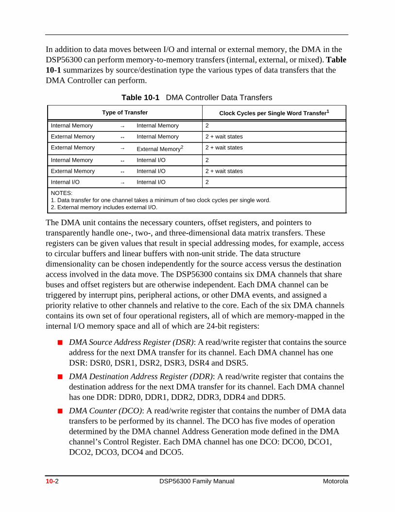
In addition to data moves between I/O and internal or external memory, the DMA inDSP56300 can perform memory-to-memory transfers (internal, external, or mixed).Table10-1 summarizes by source/destination type the various types of data transfers that DMA Controller can perform.
The DMA unit contains the necessary counters, offset registers, and pointers totransparently handle one-, two-, and three-dimensional data matrix transfers. Theseregisters can be given values that result in special addressing modes, for example, to circular buffers and linear buffers with non-unit stride. The data structuredimensionality can be chosen independently for the source access versus the destinaccess involved in the data move. The DSP56300 contains six DMA channels that sbuses and offset registers but are otherwise independent. Each DMA channel can btriggered by interrupt pins, peripheral actions, or other DMA events, and assigned apriority relative to other channels and relative to the core. Each of the six DMA chancontains its own set of four operational registers, all of which are memory-mapped iinternal I/O memory space and all of which are 24-bit registers:
■ DMA Source Address Register (DSR): A read/write register that contains the sourcaddress for the next DMA transfer for its channel. Each DMA channel has oneDSR: DSR0, DSR1, DSR2, DSR3, DSR4 and DSR5.
■ DMA Destination Address Register (DDR): A read/write register that contains thedestination address for the next DMA transfer for its channel. Each DMA chanhas one DDR: DDR0, DDR1, DDR2, DDR3, DDR4 and DDR5.
■ DMA Counter (DCO): A read/write register that contains the number of DMA datransfers to be performed by its channel. The DCO has five modes of operatiodetermined by the DMA channel Address Generation mode defined in the DMchannel’s Control Register. Each DMA channel has one DCO: DCO0, DCO1,DCO2, DCO3, DCO4 and DCO5.
Table 10-1 DMA Controller Data Transfers
Type of Transfer Clock Cycles per Single Word Transfer 1
Internal Memory → Internal Memory 2
External Memory ↔ Internal Memory 2 + wait states
External Memory → External Memory2 2 + wait states
Internal Memory ↔ Internal I/O 2
External Memory ↔ Internal I/O 2 + wait states
Internal I/O → Internal I/O 2
NOTES:1. Data transfer for one channel takes a minimum of two clock cycles per single word.2. External memory includes external I/O.
10-2 DSP56300 Family Manual Motorola
DMA Operational Overview
a3,
that
g
r
d
ctionstion
nsfer.
of
mn
e for
■ DMA Control Register (DCR): A read/write register that controls the operation ofDMA channel. Each DMA channel has one DCR: DCR0, DCR1, DCR2, DCRDCR4 and DCR5.
The DMA Controller also has supporting 24-bit registers available to all the DMAchannels:
■ DMA Offset Register (DOR): Each DOR is a read/write register that contains theoffset value to be used in some of the DMA addressing modes. The DMAcontroller has four common offset registers (DOR0, DOR1, DOR2 and DOR3)can be used by all the channels according to their Address Generation mode.
■ DMA Status Register (DSTR): This read-only register reflects the overall operatinstatus of all channels in the DMA Controller.
In summary, the DSP56300 DMA can perform I/O and memory accesses that areindependent of and frequently simultaneous with PCU operations. DMA can transfememory-to-memory and handle mixed multi-dimensional and special address modetransfers. DMA contains six highly independent channels with separate priorities anmultiple trigger choices. These capabilities significantly enhance code performance.
10.1 DMA Operational Overview
The following subsections describe how the DSP56300 DMA operates. These subseare organized by function, rather than by event sequence. The DMA register descripsection contains detailed operational information.
10.1.1 Basic Address Modes
The DSP56300 DMA can deal with the following basic types of data structures:
■ Constant Addressing: This mode uses a single address throughout the data traTypically this is used by I/O devices that use a single address to transferinformation.
■ One-dimensional: A one-dimensional matrix consisting of one item or a “line” items located in consecutive memory locations.
■ Two-dimensional: A two-dimensional matrix or table that is stored in row-coluorder with equal spacing in memory between each row or line.
■ Three-dimensional: A three-dimensional matrix or collection of tables that areequally spaced in memory.
The type of data structure is specified in the counter mode for the DMA channel. Thcounter mode divides a given 24-bit counter register into one or more sections, one
Motorola DMA Controller 10-3
DMA Operational Overview
h timethat
, oneThe
tlyused
nts ofs
ps
rdree.
oeen
; the
nsionode
e
itsatedpper
each dimension used. The appropriate counter fields either decrement or reload eacthe DMA transfers a data word. A counter field is reloaded with its initial value after field is decremented to zero. For details on counter operation, seeSection 10.5.3,"DMACounters (DCO[5 – 0])," on page 10-11. Once all fields in the counter are exhaustedor more data moves are performed and all words, lines, and tables are transferred. total collection of data moved is called the “block.” Exhaustion of the entire counterresults in a single “block transfer.” The automatic counter register updates are direcperformed on the user-visible counter register. In other words, the counter register isfor both the count load/reload function and the count decrement function.
10.1.2 Special Address Modes
The counter and offset registers can be loaded with special values to produce variathe basic addressing modes. Some examples covered in more detail in later sectioninclude:
■ Circular buffer: Use a two-dimensional counter and a negative offset that wraback to the buffer start address.
■ Linear buffer with non-unit stride: Use a two-dimensional counter with one woper row. This method must be used with byte packing, which has a stride of th
■ A larger-than-normal field width in a two-dimensional counter: Concatenate twfields in a three-dimensional counter by specifying an offset value of one betwthem.
10.1.3 Unmatched Source and Destination Dimensions
The source and destination data structures can have different dimensions.2 The datastructure with the largest dimension is read or written once during the block transferdata structure with the smaller dimension can be written or read repeatedly. For thissituation, a single counter register handles both sides of the transfer. The high-dime(three-dimensional or two-dimensional) side of the transfer determines the counter mand thus the number of available counter fields. Each “tick” of the counter counts onword transfer; that is, one source read and one destination write.
The data structure on the low-dimension side of the transfer is fully described by aright-justified subset of the counter—the number of counter fields being the same asdimension (two-dimensional or one-dimensional). This data structure access is repe(using the exact same addressing sequence) the number of times specified by the u
2. For an example, see the Motorola application report, APR/23,Using the DSP56300 Direct MemoryAccess Controller.
10-4 DSP56300 Family Manual Motorola
DMA Operational Overview
ture
MAent. A
l)
r an, not
ding
rce,ple,nnelat is
de.orre
field(s) of the counter. The pointer wraparound back to the beginning of this data strucis accomplished using a negative offset register value, similar to a circular buffer.
10.1.4 DMA Triggers (Request Sources)
Data movement in by a particular DMA channel is initiated by either a hardware or asoftware trigger. Following is an example list of some of the hardware and software Dtriggers, also known as DMA request sources. Peripheral triggers are device-dependDMA channel can be configured for triggering by only one source at a time.
■ Hardware triggers
— External interrupt pins (IRQA - IRQD)
— DMA channel block transfer completion (by this or a different DMA channe
— Peripheral status bits
— Receiver has new datum to be read by DMA
— Transmitter needs new datum from DMA to send
— Timer compare event
■ Software triggers
— DMA Enable bit for this DMA channel
A peripheral status bit that triggers an enabled DMA transfer also typically can triggeenabled peripheral interrupt. The DMA transfer is triggered by the status bit changeby the peripheral interrupt event, and the DMA transfer occurs whether or not theperipheral interrupt is enabled. Furthermore, avoid triggering a DMA transfer and aperipheral interrupt from the same event; this can result in a lack of coordination regarresources and status bit changes.
10.1.5 Transfer Mode
When a DMA channel is enabled and receives a trigger from its configured trigger souit begins moving data as soon as the needed resources become available (for examinternal DMA buses and memory locations). As a result of the trigger event, the chatransfers either all or a subset of the block (this is configurable). The amount of data thtransferred in response to each trigger event is determined by the DMA transfer moBesides the trigger data structure, the transfer mode also selects either a hardware software trigger, and automatic block repeat enable. The available transfer modes asingle word, line, and block. Typically, a DMA channel used in conjunction with aperipheral operates in a single word transfer mode (triggered by a receiver full ortransmitter empty condition).
Motorola DMA Controller 10-5
Timing (Core Clock Cycles)
gralfer
ord
actoftenate
ivenceists
el
d one
nelA
ockd by
10.2 Timing (Core Clock Cycles)
This section describes the timing of core and DMA data transfers in the context of intecore clock cycle counts. When the needed resources are available, each word transperformed by the DMA takes at least two core clock cycles:
■ Source read (at least one cycle)
■ Destination write (at least one cycle)
Any wait states incurred during external memory accesses are added to the DMA wtransfer time (for external source and/or destination).
Some peripherals (generally those using first-in-first-out (FIFO) for data transfer) mayas “fast DMA request sources.” These peripherals can trigger a new DMA request asas every two core clock cycles, thereby using the DMA at its maximum throughput rwith zero overhead time.
10.2.1 Non-Overlap Between DMA Channels
Data movement can never be performed by more than one DMA channel within a gcore clock cycle. For example, it is not possible for Channel 1 to commence its sourread before Channel 0 completes its destination write. This non-overlap limitation exfor all situations, including the following cases:
■ One channel needs to read (write) from external memory, and another channneeds to write (read) to internal memory.
■ One of the DMA channels is waiting on the Bus Interface Unit (BIU) for anexternal access to complete, and the BIU is in turn waiting because of:
— Static wait states (determined by Bus Control Register)
— Dynamic wait states (controlled byTA pin)
— Byte packing
This limitation is necessary because there is only one internal DMA address bus aninternal DMA data bus. The internal DMA buses are in use by a DMA channel evenduring the external memory access phase of the DMA word transfer. Although chanoverlap during DMA channel transfers cannot exist, zero overhead between two DMchannel transfers can exist. Once the word transfer performed by a DMA channel iscompleted, another DMA channel can begin data movement in the very next core clcycle—if the second DMA channel has already been triggered and is not being delayecontention or priority issues.
10-6 DSP56300 Family Manual Motorola
Channel Priority
ata the
rnal
has
rnal
g adntrol for
n this
ls.
of
een
10.2.2 Overlap between DMA Channel and Core
Since the core and DMA use separate address and data buses, both can perform dmovement in a given core clock cycle. This overlap of data movement can occur forfollowing cases:
■ The core is accessing internal memory while DMA is accessing a different intememory partition:
— RAM: 1/4 Kword partition size (this size is device-dependent)
— ROM: 2, 3, or 4 Kword device-specific partition size
If the core and DMA try to access the same internal memory partition, the corepriority and DMA is delayed.
■ The core is accessing internal (external) memory while DMA is accessing exte(internal) memory
10.3 Channel Priority
DMA channel priority determines if and when a DMA channel can be interrupted durinblock transfer. An interruption occurs between word transfers. The current DMA wortransfer is allowed to complete before the core or another DMA channel can take coof the resource that is under contention. The DMA channel priority arbitration occurseach DMA word transfer; only enabled and already triggered channels can take part iarbitration.
10.3.1 Priority Between DMA Channels
Each DMA channel can be independently assigned one of four possible priority leveThe treatment of priorities is as follows:
■ Channels with different priorities
A higher-priority DMA channel can interrupt a lower-priority DMA channel andcomplete its block transfer before control transfers back to the lower-prioritychannel.
■ Channels with the same priority, one of two different modes can be selected:
— Continuous mode: A DMA channel cannot interrupt another DMA channel the same priority.
— Non-continuous mode: Control is transferred in a round-robin fashion betweach channel of the same priority. Each channel transfers one word beforecontrol transfers to the next channel in this group.
Motorola DMA Controller 10-7
Channel Priority
s ofe
le. Theast
n ben corelrding
ater
ing
the
ere is
aof thee theentire toationwith
else.
DMA channels cannot interrupt each other in the middle of word transfers, regardlestheir relative priorities. A word transfer made by one DMA channel must finish beforanother DMA channel can commence a word transfer.
10.3.2 Priority Between a DMA Channel and the Core
If the core and a DMA channel are both contending for the same partition of internamemory, but neither has begun the word transfer, the core always takes precedencDMA channel must wait until the core is not accessing this memory partition for at leone core clock cycle before it can begin to access the partition.
If the DMA channel and the core are each attempting to access a different internalmemory partition in RAM or ROM, no contention exists. In this case, the accesses camade simultaneously (data movement can occur in both of these data paths in a giveclock cycle). If the core and a DMA channel are both contending to make an externamemory access, the prioritizing between that channel and the core is performed accoto one of two selectable modes:
■ Static DMA/Core Prioritizing mode — The core priority is configured to have aconstant fixed relationship with the DMA priority, regardless of which DMAchannel is considered. The core priority is set to be either lower, equal, or grethan that of the DMA. The individual DMA channels have equal priority whencompared to the core, although they may still have unequal priorities whencompared to each other. This mode is set using bits CDP[1 – 0] of the OperatMode Register.
■ Dynamic DMA/Core Prioritizing mode — The priority of each DMA channel isindividually compared with that of the core. The DMA channel priority settingused for comparison with other DMA channels is also used for comparison withcore. This mode is set using bits CP[1 – 0] of the Status Register.
Note: Even though DMA and the core have separate address and data buses, thonly one external address and data bus.
The core cannot interrupt a DMA channel in the middle of a word transfer to or fromcontended resource (an internal memory partition, or external memory), regardless core/DMA relative priority. If the DMA channel is already performing an access to thresource, the core must wait until the current DMA word transfer finishes accessingresource before the core can access that resource. The core may have to wait for theDMA word transfer to complete, or it may have to wait only for the DMA source readcomplete. This depends on the destination address of the DMA channel. If the destinof the DMA word transfer is not in the contended resource, then the core can proceedits access to the resource while the DMA performs its destination write somewhere
10-8 DSP56300 Family Manual Motorola
Special Uses of DMA With the Bus Interface Unit
y be
ideMAy, itutiveo thekes
wordletely
aytionuses
ibed in
sferan
nelfuse
a-
10.4 Special Uses of DMA With the Bus Interface Unit
The following subsections describe Bus Interface Unit (BIU) operations that can onlperformed using DMA.
10.4.1 Byte Packing
Byte packing is used when the 24-bit data width DSP core interfaces with an 8-bit wexternal memory device. Byte packing can be performed only in conjunction with a Ddata move.3 When the DMA channel attempts to read a word from the external memorexpects a 24-bit value. In accordance with the DMA read, the BIU reads three consecbytes from the memory, packs them into one 24-bit word, and then passes this word tDMA. A reverse sequence occurs for a DMA write to the external memory. The BIU tathe 24-bit word from the DMA channel, unpacks it, and writes it as three consecutivebytes, to the external memory. For both read and write, the DMA views each 24-bit transfer as a single external access. However, the byte packing operation is not comptransparent to the DMA. To read or write several 24-bit words to or from consecutivelocations in the 8-bit memory, the DMA must be programmed to either increase ordecrease its external memory address pointer by three for each 24-bit transfer.
10.4.1.1 DRAM In-Page Accesses using DMA
When a DMA channel handles several consecutive in-page DRAM word accesses, special situation can occur if an in-page access is interrupted by an external memoraccess initiated either by the core or a different DMA channel. The interrupting operacould be a higher-priority access to external SRAM. After the interrupting operation the BIU, the original DMA channel can resume reading or writing the DRAM withoutlosing in-page access. This can occur as long as all in-page access conditions (descrChapter 9, External Memory Interface (Port A)) remain satisfied.
10.4.1.2 End-of-Block-Transfer Interrupt
Upon completion of a block transfer by a DMA channel, an optional end-of-block-tranDMA interrupt can be generated. The interrupt service routine (ISR) called by such interrupt can perform any functions needed at this time. For example, the ISR couldreconfigure the DMA channel for the next data block transfer or restart the DMA chan(if it is used in a transfer mode for which no automatic restart is available). Do not conan end-of-block-transfer DMA interrupt, also known as a “DMA interrupt,” with aperipheral interrupt. A peripheral interrupt can be generated by the same event thattriggers the DMA channel to move part or all of the block.
3. For details, see the Port A Address Attribute Register description in Chapter 9 and the Motorola appliction report, APR23/D,Using the DSP56300 Direct Memory Access Controller.
Motorola DMA Controller 10-9
DMA Controller Programming Model
ssets of
bye,
fer.
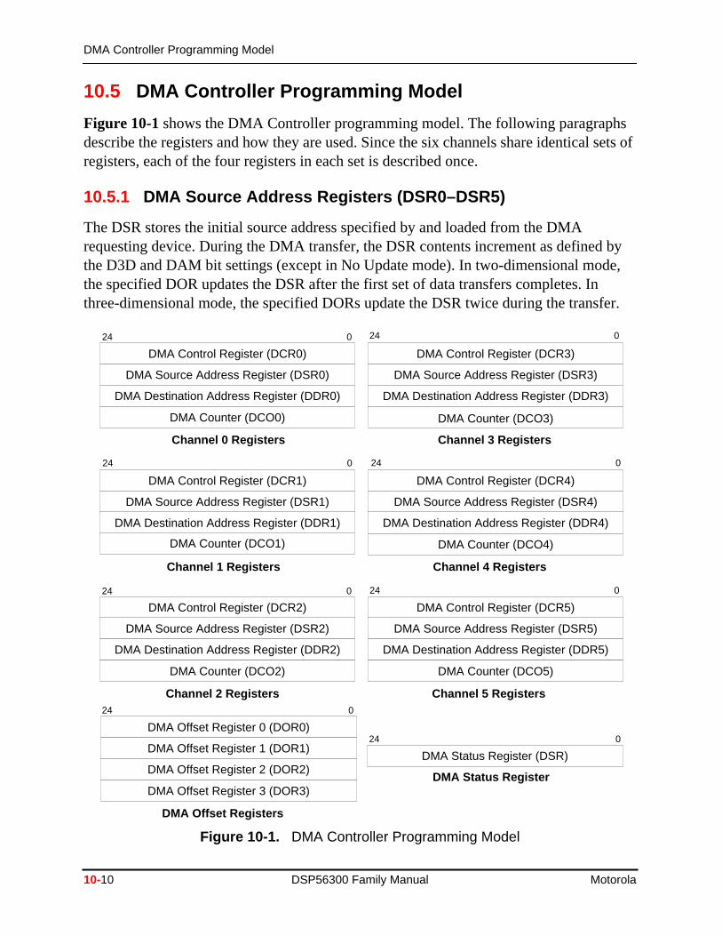
10.5 DMA Controller Programming Model
Figure 10-1 shows the DMA Controller programming model. The following paragraphdescribe the registers and how they are used. Since the six channels share identicalregisters, each of the four registers in each set is described once.
10.5.1 DMA Source Address Registers (DSR0–DSR5)
The DSR stores the initial source address specified by and loaded from the DMArequesting device. During the DMA transfer, the DSR contents increment as definedthe D3D and DAM bit settings (except in No Update mode). In two-dimensional modthe specified DOR updates the DSR after the first set of data transfers completes. Inthree-dimensional mode, the specified DORs update the DSR twice during the trans
Figure 10-1. DMA Controller Programming Model
DMA Control Register (DCR5)
DMA Source Address Register (DSR5)
DMA Destination Address Register (DDR5)
DMA Counter (DCO5)
DMA Control Register (DCR4)
DMA Source Address Register (DSR4)
DMA Destination Address Register (DDR4)
DMA Counter (DCO4)
DMA Control Register (DCR3)
DMA Source Address Register (DSR3)
DMA Destination Address Register (DDR3)
DMA Counter (DCO3)
DMA Control Register (DCR2)
DMA Source Address Register (DSR2)
DMA Destination Address Register (DDR2)
DMA Counter (DCO2)
DMA Control Register (DCR1)
DMA Source Address Register (DSR1)
DMA Destination Address Register (DDR1)
DMA Counter (DCO1)
DMA Control Register (DCR0)
DMA Source Address Register (DSR0)
DMA Destination Address Register (DDR0)
DMA Counter (DCO0)
Channel 0 Registers
Channel 1 Registers
Channel 2 Registers
Channel 3 Registers
Channel 4 Registers
Channel 5 Registers
DMA Offset Register 0 (DOR0)
DMA Offset Register 1 (DOR1)
DMA Offset Register 2 (DOR2)
DMA Offset Register 3 (DOR3)
DMA Offset Registers
DMA Status Register (DSR)
DMA Status Register
024
024
024
024
024 024
024
024
10-10 DSP56300 Family Manual Motorola
DMA Controller Programming Model
A bye,
fer.
the
ess
ter.
fored on
isress
CO is
alue
10.5.2 DMA Destination Address Registers (DDR[5 – 0])
The DDR stores the initial destination address specified by and loaded from the DMrequesting device. During the DMA transfer, the DDR contents increment as definedthe D3D and DAM bit settings (except in No Update mode). In two-dimensional modthe specified DOR updates the DDR after the first set of data transfers completes. Inthree-dimensional mode, the specified DORs update the DDR twice during the trans
10.5.3 DMA Counters (DCO[5 – 0])
During DMA operation, a Source Address Register (DSR) is associated with one of counter modes, and the Destination Address Register (DDR) can be associated withanother counter mode. The following examples use DSR as an example of the addrregister used, but the same example is valid for the DDR.
10.5.3.1 DMA Counter Mode A—Single Counter
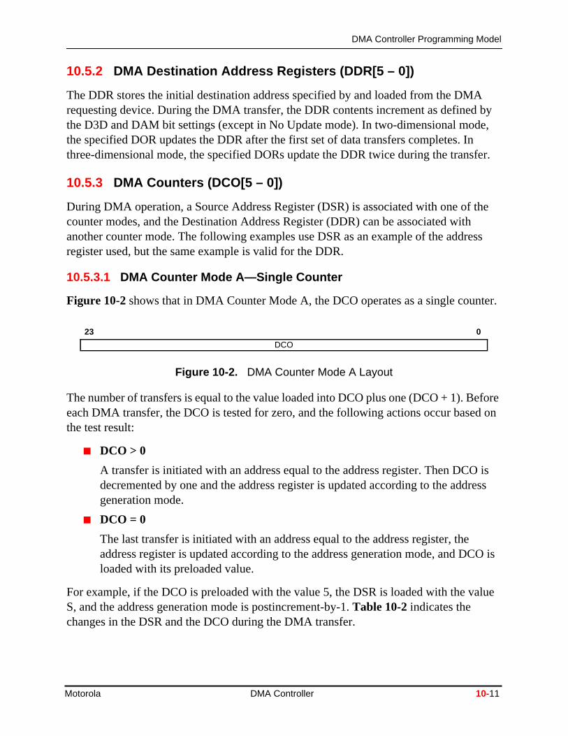
Figure 10-2 shows that in DMA Counter Mode A, the DCO operates as a single coun
The number of transfers is equal to the value loaded into DCO plus one (DCO + 1). Beeach DMA transfer, the DCO is tested for zero, and the following actions occur basethe test result:
■ DCO > 0
A transfer is initiated with an address equal to the address register. Then DCOdecremented by one and the address register is updated according to the addgeneration mode.
■ DCO = 0
The last transfer is initiated with an address equal to the address register, theaddress register is updated according to the address generation mode, and Dloaded with its preloaded value.
For example, if the DCO is preloaded with the value 5, the DSR is loaded with the vS, and the address generation mode is postincrement-by-1.Table 10-2 indicates thechanges in the DSR and the DCO during the DMA transfer.
Figure 10-2. DMA Counter Mode A Layout
23 0
DCO
Motorola DMA Controller 10-11
DMA Controller Programming Model
l
L is
ssd by
OH
R is
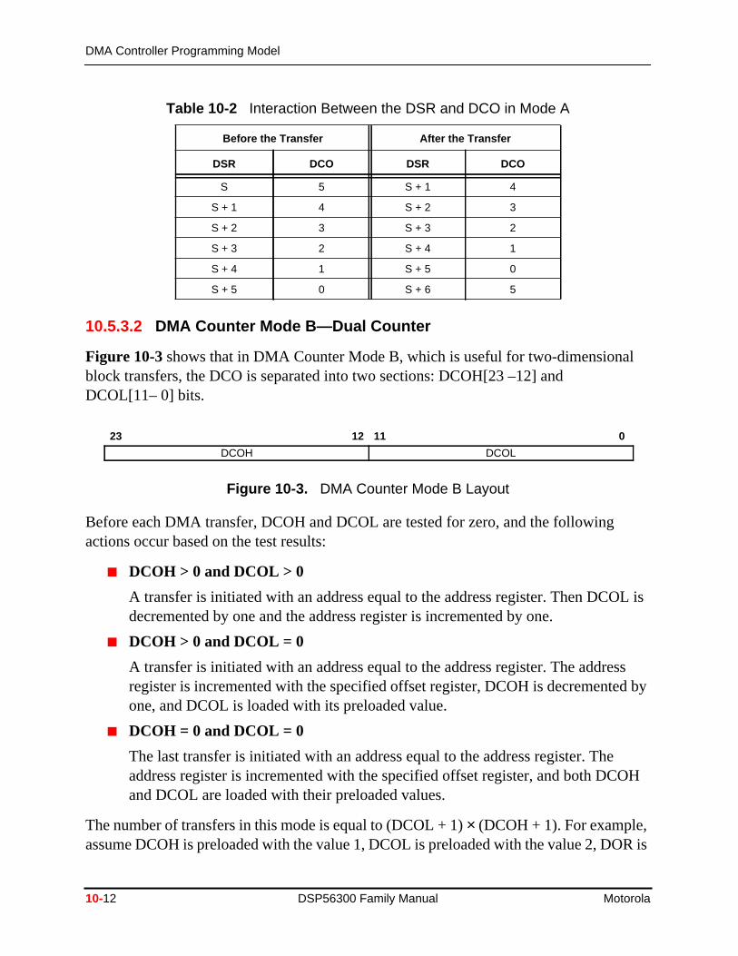
10.5.3.2 DMA Counter Mode B—Dual Counter
Figure 10-3 shows that in DMA Counter Mode B, which is useful for two-dimensionablock transfers, the DCO is separated into two sections: DCOH[23 –12] andDCOL[11– 0] bits.
Before each DMA transfer, DCOH and DCOL are tested for zero, and the followingactions occur based on the test results:
■ DCOH > 0 and DCOL > 0
A transfer is initiated with an address equal to the address register. Then DCOdecremented by one and the address register is incremented by one.
■ DCOH > 0 and DCOL = 0
A transfer is initiated with an address equal to the address register. The addreregister is incremented with the specified offset register, DCOH is decrementeone, and DCOL is loaded with its preloaded value.
■ DCOH = 0 and DCOL = 0
The last transfer is initiated with an address equal to the address register. Theaddress register is incremented with the specified offset register, and both DCand DCOL are loaded with their preloaded values.
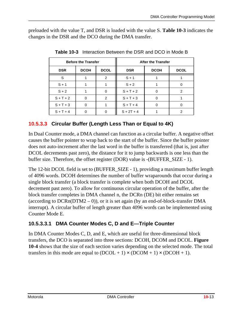
The number of transfers in this mode is equal to (DCOL + 1)× (DCOH + 1). For example,assume DCOH is preloaded with the value 1, DCOL is preloaded with the value 2, DO
Table 10-2 Interaction Between the DSR and DCO in Mode A
Before the Transfer After the Transfer
DSR DCO DSR DCO
S 5 S + 1 4
S + 1 4 S + 2 3
S + 2 3 S + 3 2
S + 3 2 S + 4 1
S + 4 1 S + 5 0
S + 5 0 S + 6 5
Figure 10-3. DMA Counter Mode B Layout
23 12 11 0
DCOH DCOL
10-12 DSP56300 Family Manual Motorola
DMA Controller Programming Model
fsetnterfter the
thing a
he
sing
e total
preloaded with the value T, and DSR is loaded with the value S.Table 10-3 indicates thechanges in the DSR and the DCO during the DMA transfer.
10.5.3.3 Circular Buffer (Length Less Than or Equal to 4K)
In Dual Counter mode, a DMA channel can function as a circular buffer. A negative ofcauses the buffer pointer to wrap back to the start of the buffer. Since the buffer poidoes not auto-increment after the last word in the buffer is transferred (that is, just aDCOL decrements past zero), the distance for it to jump backwards is one less thanbuffer size. Therefore, the offset register (DOR) value is -(BUFFER_SIZE - 1).
The 12-bit DCOL field is set to (BUFFER_SIZE - 1), providing a maximum buffer lengof 4096 words. DCOH determines the number of buffer wraparounds that occur dursingle block transfer (a block transfer is complete when both DCOH and DCOLdecrement past zero). To allow for continuous circular operation of the buffer, after tblock transfer completes in DMA channel n, the DCRn (DE) bit either remains set(according to DCRn(DTM2 – 0)), or it is set again (by an end-of-block-transfer DMAinterrupt). A circular buffer of length greater than 4096 words can be implemented uCounter Mode E.
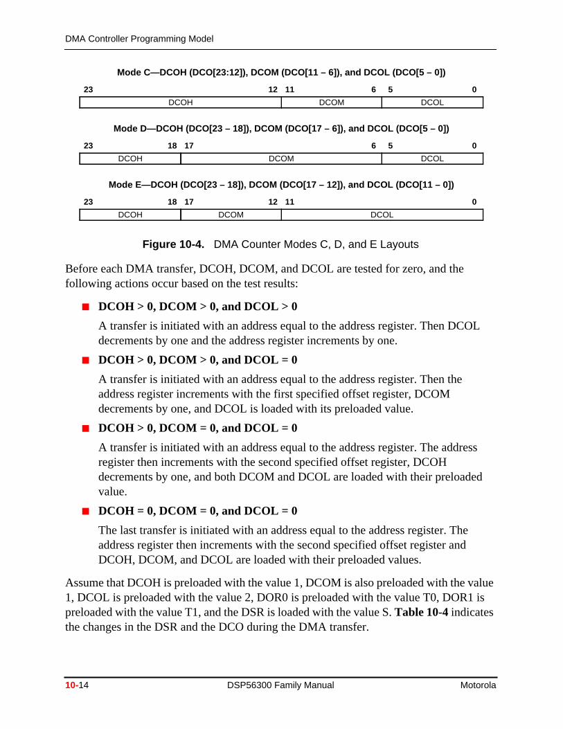
10.5.3.3.1 DMA Counter Modes C, D and E—Triple Counter
In DMA Counter Modes C, D, and E, which are useful for three-dimensional blocktransfers, the DCO is separated into three sections: DCOH, DCOM and DCOL.Figure10-4 shows that the size of each section varies depending on the selected mode. Thtransfers in this mode are equal to (DCOL + 1)× (DCOM + 1)× (DCOH + 1).
Table 10-3 Interaction Between the DSR and DCO in Mode B
Before the Transfer After the Transfer
DSR DCOH DCOL DSR DCOH DCOL
S 1 2 S + 1 1 1
S + 1 1 1 S + 2 1 0
S + 2 1 0 S + T + 2 0 2
S + T + 2 0 2 S + T + 3 0 1
S + T + 3 0 1 S + T + 4 0 0
S + T + 4 0 0 S + 2T + 4 1 2
Motorola DMA Controller 10-13
DMA Controller Programming Model
L
ss
ed
alue is
Figure 10-4. DMA Counter Modes C, D, and E Layouts
Before each DMA transfer, DCOH, DCOM, and DCOL are tested for zero, and thefollowing actions occur based on the test results:
■ DCOH > 0, DCOM > 0, and DCOL > 0
A transfer is initiated with an address equal to the address register. Then DCOdecrements by one and the address register increments by one.
■ DCOH > 0, DCOM > 0, and DCOL = 0
A transfer is initiated with an address equal to the address register. Then theaddress register increments with the first specified offset register, DCOMdecrements by one, and DCOL is loaded with its preloaded value.
■ DCOH > 0, DCOM = 0, and DCOL = 0
A transfer is initiated with an address equal to the address register. The addreregister then increments with the second specified offset register, DCOHdecrements by one, and both DCOM and DCOL are loaded with their preloadvalue.
■ DCOH = 0, DCOM = 0, and DCOL = 0
The last transfer is initiated with an address equal to the address register. Theaddress register then increments with the second specified offset register andDCOH, DCOM, and DCOL are loaded with their preloaded values.
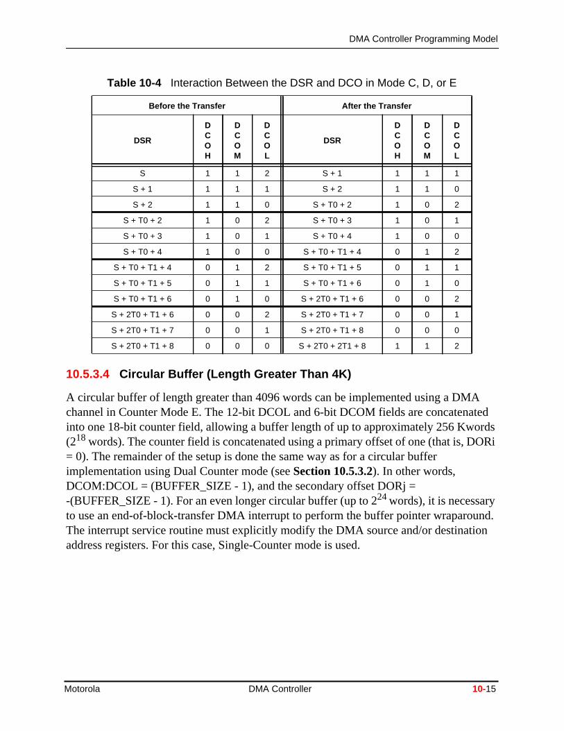
Assume that DCOH is preloaded with the value 1, DCOM is also preloaded with the v1, DCOL is preloaded with the value 2, DOR0 is preloaded with the value T0, DOR1preloaded with the value T1, and the DSR is loaded with the value S.Table 10-4indicatesthe changes in the DSR and the DCO during the DMA transfer.
Mode C—DCOH (DCO[23:12]), DCOM (DCO[11 – 6]), and DCOL (DCO[5 – 0])
Mode D—DCOH (DCO[23 – 18]), DCOM (DCO[17 – 6]), and DCOL (DCO[5 – 0]).
Mode E—DCOH (DCO[23 – 18]), DCOM (DCO[17 – 12]), and DCOL (DCO[11 – 0])
23 12 11 6 5 0
DCOH DCOM DCOL
23 18 17 6 5 0
DCOH DCOM DCOL
23 18 17 12 11 0
DCOH DCOM DCOL
10-14 DSP56300 Family Manual Motorola
DMA Controller Programming Model
AteddsORi
nd.on
10.5.3.4 Circular Buffer (Length Greater Than 4K)
A circular buffer of length greater than 4096 words can be implemented using a DMchannel in Counter Mode E. The 12-bit DCOL and 6-bit DCOM fields are concatenainto one 18-bit counter field, allowing a buffer length of up to approximately 256 Kwor(218 words). The counter field is concatenated using a primary offset of one (that is, D= 0). The remainder of the setup is done the same way as for a circular bufferimplementation using Dual Counter mode (seeSection 10.5.3.2). In other words,DCOM:DCOL = (BUFFER_SIZE - 1), and the secondary offset DORj =-(BUFFER_SIZE - 1). For an even longer circular buffer (up to 224words), it is necessaryto use an end-of-block-transfer DMA interrupt to perform the buffer pointer wraparouThe interrupt service routine must explicitly modify the DMA source and/or destinatiaddress registers. For this case, Single-Counter mode is used.
Table 10-4 Interaction Between the DSR and DCO in Mode C, D, or E
Before the Transfer After the Transfer
DSR
DCOH
DCOM
DCOL
DSR
DCOH
DCOM
DCOL
S 1 1 2 S + 1 1 1 1
S + 1 1 1 1 S + 2 1 1 0
S + 2 1 1 0 S + T0 + 2 1 0 2
S + T0 + 2 1 0 2 S + T0 + 3 1 0 1
S + T0 + 3 1 0 1 S + T0 + 4 1 0 0
S + T0 + 4 1 0 0 S + T0 + T1 + 4 0 1 2
S + T0 + T1 + 4 0 1 2 S + T0 + T1 + 5 0 1 1
S + T0 + T1 + 5 0 1 1 S + T0 + T1 + 6 0 1 0
S + T0 + T1 + 6 0 1 0 S + 2T0 + T1 + 6 0 0 2
S + 2T0 + T1 + 6 0 0 2 S + 2T0 + T1 + 7 0 0 1
S + 2T0 + T1 + 7 0 0 1 S + 2T0 + T1 + 8 0 0 0
S + 2T0 + T1 + 8 0 0 0 S + 2T0 + 2T1 + 8 1 1 2
Motorola DMA Controller 10-15
DMA Controller Programming Model
Assor
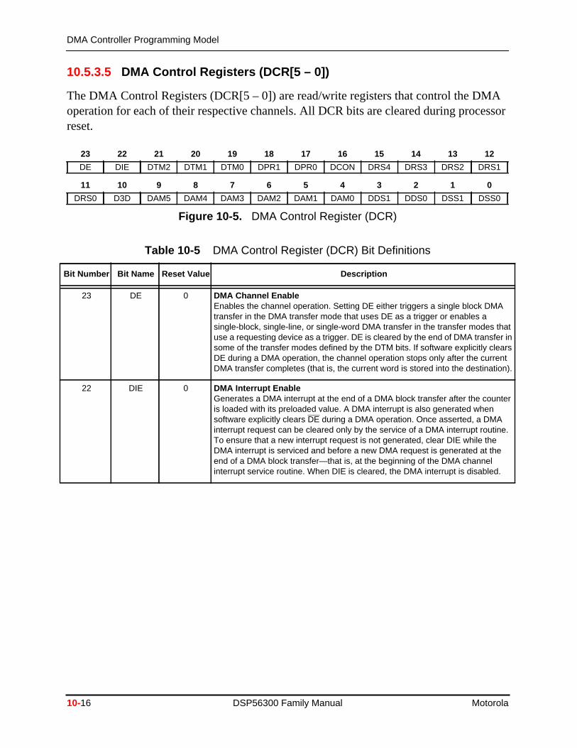
10.5.3.5 DMA Control Registers (DCR[5 – 0])
The DMA Control Registers (DCR[5 – 0]) are read/write registers that control the DMoperation for each of their respective channels. All DCR bits are cleared during procereset.
Figure 10-5. DMA Control Register (DCR)
Table 10-5 DMA Control Register (DCR) Bit Definitions
Bit Number Bit Name Reset Value Description
23 DE 0 DMA Channel EnableEnables the channel operation. Setting DE either triggers a single block DMAtransfer in the DMA transfer mode that uses DE as a trigger or enables asingle-block, single-line, or single-word DMA transfer in the transfer modes thatuse a requesting device as a trigger. DE is cleared by the end of DMA transfer insome of the transfer modes defined by the DTM bits. If software explicitly clearsDE during a DMA operation, the channel operation stops only after the currentDMA transfer completes (that is, the current word is stored into the destination).
22 DIE 0 DMA Interrupt EnableGenerates a DMA interrupt at the end of a DMA block transfer after the counteris loaded with its preloaded value. A DMA interrupt is also generated whensoftware explicitly clears DE during a DMA operation. Once asserted, a DMAinterrupt request can be cleared only by the service of a DMA interrupt routine.To ensure that a new interrupt request is not generated, clear DIE while theDMA interrupt is serviced and before a new DMA request is generated at theend of a DMA block transfer—that is, at the beginning of the DMA channelinterrupt service routine. When DIE is cleared, the DMA interrupt is disabled.
23 22 21 20 19 18 17 16 15 14 13 12
DE DIE DTM2 DTM1 DTM0 DPR1 DPR0 DCON DRS4 DRS3 DRS2 DRS1
11 10 9 8 7 6 5 4 3 2 1 0
DRS0 D3D DAM5 DAM4 DAM3 DAM2 DAM1 DAM0 DDS1 DDS0 DSS1 DSS0
10-16 DSP56300 Family Manual Motorola
DMA Controller Programming Model
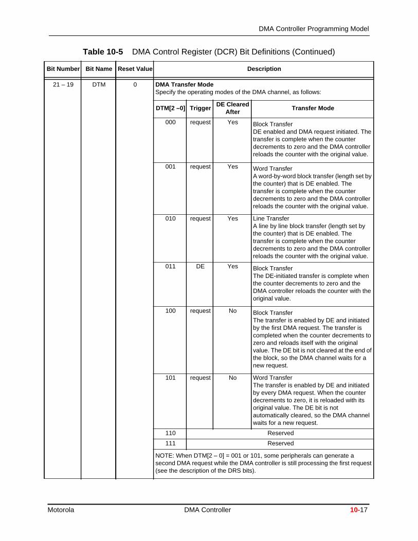
21 – 19 DTM 0 DMA Transfer ModeSpecify the operating modes of the DMA channel, as follows:
DTM[2 –0] TriggerDE Cleared
AfterTransfer Mode
000 request Yes Block TransferDE enabled and DMA request initiated. Thetransfer is complete when the counterdecrements to zero and the DMA controllerreloads the counter with the original value.
001 request Yes Word TransferA word-by-word block transfer (length set bythe counter) that is DE enabled. Thetransfer is complete when the counterdecrements to zero and the DMA controllerreloads the counter with the original value.
010 request Yes Line TransferA line by line block transfer (length set bythe counter) that is DE enabled. Thetransfer is complete when the counterdecrements to zero and the DMA controllerreloads the counter with the original value.
011 DE Yes Block TransferThe DE-initiated transfer is complete whenthe counter decrements to zero and theDMA controller reloads the counter with theoriginal value.
100 request No Block TransferThe transfer is enabled by DE and initiatedby the first DMA request. The transfer iscompleted when the counter decrements tozero and reloads itself with the originalvalue. The DE bit is not cleared at the end ofthe block, so the DMA channel waits for anew request.
101 request No Word TransferThe transfer is enabled by DE and initiatedby every DMA request. When the counterdecrements to zero, it is reloaded with itsoriginal value. The DE bit is notautomatically cleared, so the DMA channelwaits for a new request.
110 Reserved
111 Reserved
NOTE: When DTM[2 – 0] = 001 or 101, some peripherals can generate asecond DMA request while the DMA controller is still processing the first request(see the description of the DRS bits).
Table 10-5 DMA Control Register (DCR) Bit Definitions (Continued)
Bit Number Bit Name Reset Value Description
Motorola DMA Controller 10-17
DMA Controller Programming Model
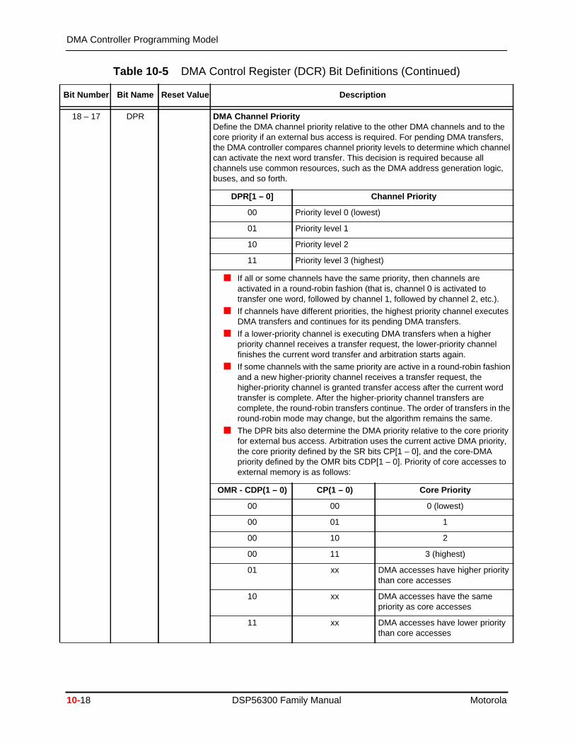
18 – 17 DPR DMA Channel PriorityDefine the DMA channel priority relative to the other DMA channels and to thecore priority if an external bus access is required. For pending DMA transfers,the DMA controller compares channel priority levels to determine which channelcan activate the next word transfer. This decision is required because allchannels use common resources, such as the DMA address generation logic,buses, and so forth.
DPR[1 – 0] Channel Priority
00 Priority level 0 (lowest)
01 Priority level 1
10 Priority level 2
11 Priority level 3 (highest)
■ If all or some channels have the same priority, then channels areactivated in a round-robin fashion (that is, channel 0 is activated totransfer one word, followed by channel 1, followed by channel 2, etc.).
■ If channels have different priorities, the highest priority channel executesDMA transfers and continues for its pending DMA transfers.
■ If a lower-priority channel is executing DMA transfers when a higherpriority channel receives a transfer request, the lower-priority channelfinishes the current word transfer and arbitration starts again.
■ If some channels with the same priority are active in a round-robin fashionand a new higher-priority channel receives a transfer request, thehigher-priority channel is granted transfer access after the current wordtransfer is complete. After the higher-priority channel transfers arecomplete, the round-robin transfers continue. The order of transfers in theround-robin mode may change, but the algorithm remains the same.
■ The DPR bits also determine the DMA priority relative to the core priorityfor external bus access. Arbitration uses the current active DMA priority,the core priority defined by the SR bits CP[1 – 0], and the core-DMApriority defined by the OMR bits CDP[1 – 0]. Priority of core accesses toexternal memory is as follows:
OMR - CDP(1 – 0) CP(1 – 0) Core Priority
00 00 0 (lowest)
00 01 1
00 10 2
00 11 3 (highest)
01 xx DMA accesses have higher prioritythan core accesses
10 xx DMA accesses have the samepriority as core accesses
11 xx DMA accesses have lower prioritythan core accesses
Table 10-5 DMA Control Register (DCR) Bit Definitions (Continued)
Bit Number Bit Name Reset Value Description
10-18 DSP56300 Family Manual Motorola
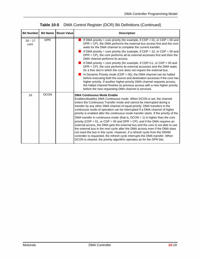
DMA Controller Programming Model
18 – 17cont.
DPR ■ If DMA priority > core priority (for example, if CDP = 01, or CDP = 00 andDPR > CP), the DMA performs the external bus access first and the corewaits for the DMA channel to complete the current transfer.
■ If DMA priority = core priority (for example, if CDP = 10, or CDP = 00 andDPR = CP), the core performs all its external accesses first and then theDMA channel performs its access.
■ If DMA priority < core priority (for example, if CDP=11, or CDP = 00 andDPR < CP), the core performs its external accesses and the DMA waitsfor a free slot in which the core does not require the external bus.
■ In Dynamic Priority mode (CDP = 00), the DMA channel can be haltedbefore executing both the source and destination accesses if the core hashigher priority. If another higher-priority DMA channel requests access,the halted channel finishes its previous access with a new higher prioritybefore the new requesting DMA channel is serviced.
16 DCON DMA Continuous Mode EnableEnables/disables DMA Continuous mode. When DCON is set, the channelenters the Continuous Transfer mode and cannot be interrupted during atransfer by any other DMA channel of equal priority. DMA transfers in thecontinuous mode of operation can be interrupted if a DMA channel of higherpriority is enabled after the continuous mode transfer starts. If the priority of theDMA transfer in continuous mode (that is, DCON = 1) is higher than the corepriority (CDP = 01, or CDP = 00 and DPR > CP), and if the DMA requires anexternal access, the DMA gets the external bus and the core is not able to usethe external bus in the next cycle after the DMA access even if the DMA doesnot need the bus in this cycle. However, if a refresh cycle from the DRAMcontroller is requested, the refresh cycle interrupts the DMA transfer. WhenDCON is cleared, the priority algorithm operates as for the DPR bits.
Table 10-5 DMA Control Register (DCR) Bit Definitions (Continued)
Bit Number Bit Name Reset Value Description
Motorola DMA Controller 10-19
DMA Controller Programming Model
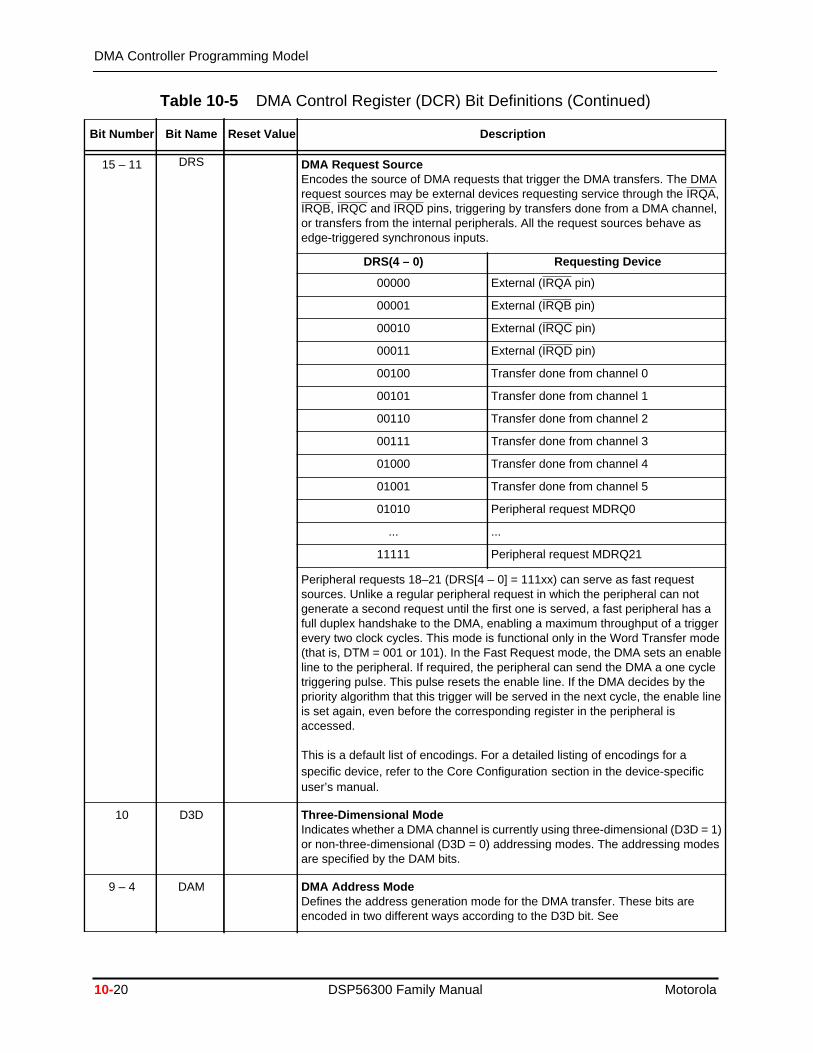
15 – 11 DRS DMA Request SourceEncodes the source of DMA requests that trigger the DMA transfers. The DMArequest sources may be external devices requesting service through the IRQA,IRQB, IRQC and IRQD pins, triggering by transfers done from a DMA channel,or transfers from the internal peripherals. All the request sources behave asedge-triggered synchronous inputs.
DRS(4 – 0) Requesting Device
00000 External (IRQA pin)
00001 External (IRQB pin)
00010 External (IRQC pin)
00011 External (IRQD pin)
00100 Transfer done from channel 0
00101 Transfer done from channel 1
00110 Transfer done from channel 2
00111 Transfer done from channel 3
01000 Transfer done from channel 4
01001 Transfer done from channel 5
01010 Peripheral request MDRQ0
... ...
11111 Peripheral request MDRQ21
Peripheral requests 18–21 (DRS[4 – 0] = 111xx) can serve as fast requestsources. Unlike a regular peripheral request in which the peripheral can notgenerate a second request until the first one is served, a fast peripheral has afull duplex handshake to the DMA, enabling a maximum throughput of a triggerevery two clock cycles. This mode is functional only in the Word Transfer mode(that is, DTM = 001 or 101). In the Fast Request mode, the DMA sets an enableline to the peripheral. If required, the peripheral can send the DMA a one cycletriggering pulse. This pulse resets the enable line. If the DMA decides by thepriority algorithm that this trigger will be served in the next cycle, the enable lineis set again, even before the corresponding register in the peripheral isaccessed.
This is a default list of encodings. For a detailed listing of encodings for aspecific device, refer to the Core Configuration section in the device-specificuser’s manual.
10 D3D Three-Dimensional ModeIndicates whether a DMA channel is currently using three-dimensional (D3D = 1)or non-three-dimensional (D3D = 0) addressing modes. The addressing modesare specified by the DAM bits.
9 – 4 DAM DMA Address ModeDefines the address generation mode for the DMA transfer. These bits areencoded in two different ways according to the D3D bit. See
Table 10-5 DMA Control Register (DCR) Bit Definitions (Continued)
Bit Number Bit Name Reset Value Description
10-20 DSP56300 Family Manual Motorola
DMA Controller Programming Model
but, they
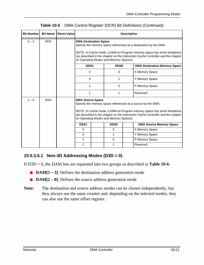
10.5.3.5.1 Non-3D Addressing Modes (D3D = 0)
If D3D = 0, the DAM bits are separated into two groups as described inTable 10-6:
■ DAM[5 – 3]: Defines the destination address generation mode
■ DAM[2 – 0]: Defines the source address generation mode
Note: The destination and source address modes can be chosen independently,they always use the same counter and, depending on the selected modescan also use the same offset register.
3 – 2 DDS DMA Destination SpaceSpecify the memory space referenced as a destination by the DMA.
NOTE: In Cache mode, a DMA-to-Program memory space has some limitations(as described in the chapter on the Instruction Cache Controller and the chapteron Operating Modes and Memory Spaces).
DDS1 DDS0 DMA Destination Memory Space
0 0 X Memory Space
0 1 Y Memory Space
1 0 P Memory Space
1 1 Reserved
1 – 0 DSS DMA Source SpaceSpecify the memory space referenced as a source by the DMA.
NOTE: In Cache mode, a DMA-to-Program memory space has some limitations(as described in the chapter on the Instruction Cache Controller and the chapteron Operating Modes and Memory Spaces).
DSS1 DSS0 DMA Source Memory Space
0 0 X Memory Space
0 1 Y Memory Space
1 0 P Memory Space
1 1 Reserved
Table 10-5 DMA Control Register (DCR) Bit Definitions (Continued)
Bit Number Bit Name Reset Value Description
Motorola DMA Controller 10-21
DMA Controller Programming Model
r. other
h the
r ahef times
is
tion ofnal)—can
gister
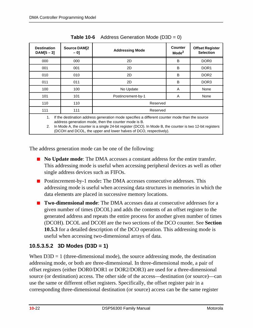
The address generation mode can be one of the following:
■ No Update mode: The DMA accesses a constant address for the entire transfeThis addressing mode is useful when accessing peripheral devices as well assingle address devices such as FIFOs.
■ Postincrement-by-1 mode: The DMA accesses consecutive addresses. Thisaddressing mode is useful when accessing data structures in memories in whicdata elements are placed in successive memory locations.
■ Two-dimensional mode: The DMA accesses data at consecutive addresses fogiven number of times (DCOL) and adds the contents of an offset register to tgenerated address and repeats the entire process for another given number o(DCOH). DCOL and DCOH are the two sections of the DCO counter. SeeSection10.5.3 for a detailed description of the DCO operation. This addressing mode useful when accessing two-dimensional arrays of data.
10.5.3.5.2 3D Modes (D3D = 1)
When D3D = 1 (three-dimensional mode), the source addressing mode, the destinaaddressing mode, or both are three-dimensional. In three-dimensional mode, a pairoffset registers (either DOR0/DOR1 or DOR2/DOR3) are used for a three-dimensiosource (or destination) access. The other side of the access—destination (or sourceuse the same or different offset registers. Specifically, the offset register pair in acorresponding three-dimensional destination (or source) access can be the same re
Table 10-6 Address Generation Mode (D3D = 0)
DestinationDAM[5 – 3]
Source DAM[2– 0]
Addressing ModeCounter
Mode2Offset Register
Selection
000 000 2D B DOR0
001 001 2D B DOR1
010 010 2D B DOR2
011 011 2D B DOR3
100 100 No Update A None
101 101 Postincrement-by-1 A None
110 110 Reserved
111 111 Reserved
1. If the destination address generation mode specifies a different counter mode than the sourceaddress generation mode, then the counter mode is B.
2. In Mode A, the counter is a single 24-bit register (DCO). In Mode B, the counter is two 12-bit registers(DCOH and DCOL, the upper and lower halves of DCO, respectively).
10-22 DSP56300 Family Manual Motorola
DMA Controller Programming Model
sters.
5 – 0]
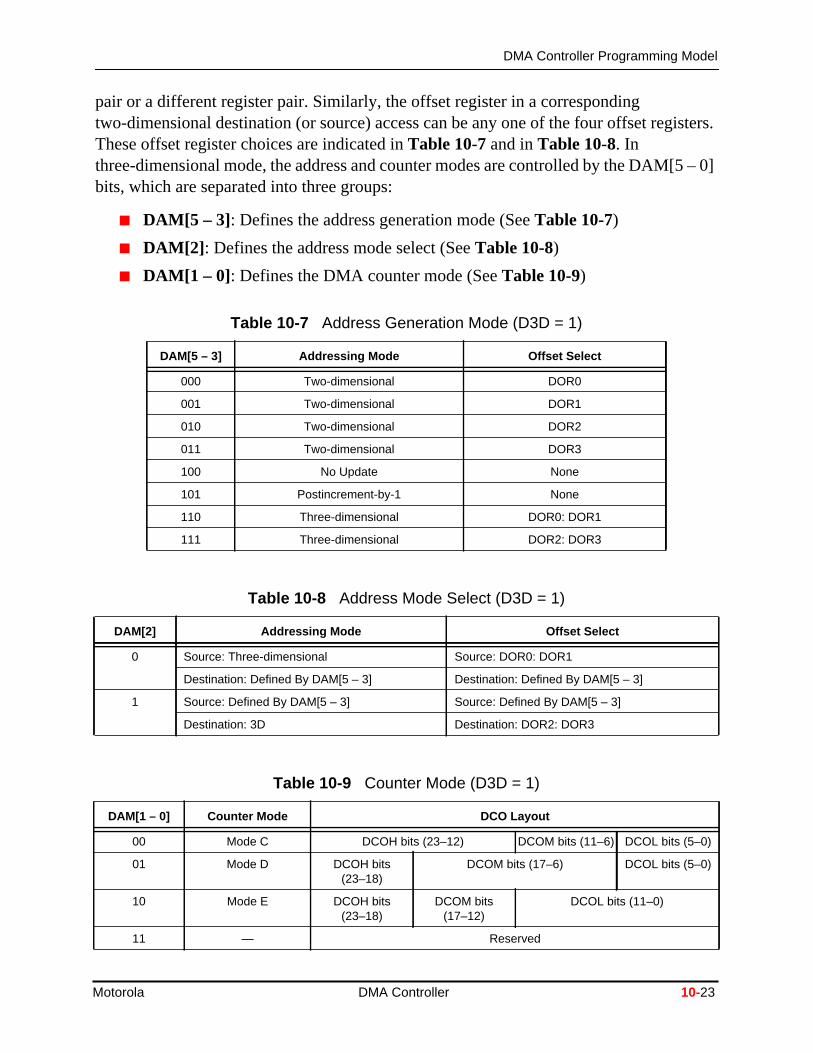
pair or a different register pair. Similarly, the offset register in a correspondingtwo-dimensional destination (or source) access can be any one of the four offset regiThese offset register choices are indicated inTable 10-7 and inTable 10-8. Inthree-dimensional mode, the address and counter modes are controlled by the DAM[bits, which are separated into three groups:
■ DAM[5 – 3]: Defines the address generation mode (SeeTable 10-7)
■ DAM[2] : Defines the address mode select (SeeTable 10-8)
■ DAM[1 – 0]: Defines the DMA counter mode (SeeTable 10-9)
Table 10-7 Address Generation Mode (D3D = 1)
DAM[5 – 3] Addressing Mode Offset Select
000 Two-dimensional DOR0
001 Two-dimensional DOR1
010 Two-dimensional DOR2
011 Two-dimensional DOR3
100 No Update None
101 Postincrement-by-1 None
110 Three-dimensional DOR0: DOR1
111 Three-dimensional DOR2: DOR3
Table 10-8 Address Mode Select (D3D = 1)
DAM[2] Addressing Mode Offset Select
0 Source: Three-dimensional Source: DOR0: DOR1
Destination: Defined By DAM[5 – 3] Destination: Defined By DAM[5 – 3]
1 Source: Defined By DAM[5 – 3] Source: Defined By DAM[5 – 3]
Destination: 3D Destination: DOR2: DOR3
Table 10-9 Counter Mode (D3D = 1)
DAM[1 – 0] Counter Mode DCO Layout
00 Mode C DCOH bits (23–12) DCOM bits (11–6) DCOL bits (5–0)
01 Mode D DCOH bits(23–18)
DCOM bits (17–6) DCOL bits (5–0)
10 Mode E DCOH bits(23–18)
DCOM bits(17–12)
DCOL bits (11–0)
11 — Reserved
Motorola DMA Controller 10-23
DMA Controller Programming Model
utivesetf timesocessee
er of
ter. Ifed to, two
theuse
ned
es of
s of
In Three-dimensional Address Generation mode, the DMA accesses data at consecaddresses for a given number of times (DCOL) and then adds the contents of an offregister to the generated address. This process repeats for another given number o(DCOM) after which another offset is added to the generated address. The entire prrepeats for a given number of times (DCOH). DCOL, DCOM, and DCOH are the thrsections of the DCO counter. SeeSection 10.5.3,"DMA Counters (DCO[5 – 0])," on page10-11 for details on the DCO operation. This addressing mode is useful when a numbtwo-dimensional arrays of data are accessed. The Offset Select entries inTable 10-7 andTable 10-8define the offset registers that are selected to increment the address regisone side of the transfer uses two-dimensional mode, only one offset register is needincrement the address register for that side of the transfer. In three-dimensional modeoffset registers are needed.
10.5.3.6 DMA Offset Registers (DOR[3 – 0])
The DMA Offset Registers (DOR[3 – 0]) are four 24-bit read/write registers that storeoffset values required by some DMA addressing modes. All two-dimensional transfersone offset register. All three-dimensional transfers use two offset registers. Refer toSection 10.5.3.5.1,"Non-3D Addressing Modes (D3D = 0)," on page 10-21 andSection10.5.3.5.2,"3D Modes (D3D = 1)," on page 10-22 for details on how DORs are assigand used. Examples of DOR usage are provided inSection 10.5.3,"DMA Counters(DCO[5 – 0])," on page 10-11 as part of the discussion about the various counter modoperation.
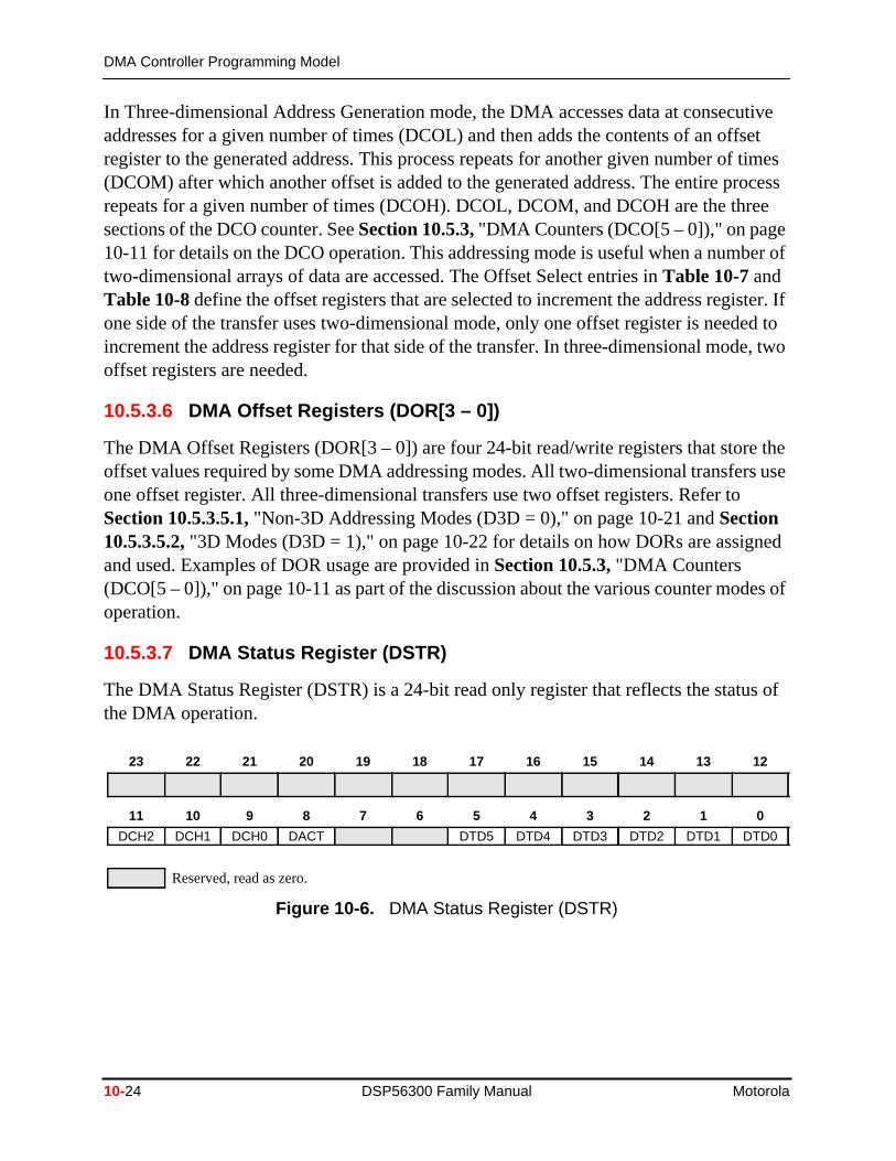
10.5.3.7 DMA Status Register (DSTR)
The DMA Status Register (DSTR) is a 24-bit read only register that reflects the statuthe DMA operation.
Figure 10-6. DMA Status Register (DSTR)
23 22 21 20 19 18 17 16 15 14 13 12
11 10 9 8 7 6 5 4 3 2 1 0
DCH2 DCH1 DCH0 DACT DTD5 DTD4 DTD3 DTD2 DTD1 DTD0
Reserved, read as zero.
10-24 DSP56300 Family Manual Motorola
DMA Controller Programming Model
Table 10-10 DMA Status Register (DSTR) Bit Definitions
Bit Number Bit Name Reset Value Description
23 – 12 0 Reserved. Write to zero for future compatibility.
11 – 9 DCH 0 DMA Active ChannelIndicate the currently active channel. The value of the DCH bits is validonly if Bit 8 DACT = 1.
DCH(2 – 0) Active Channel
000 DMA Channel 0
001 DMA Channel 1
010 DMA Channel 2
011 DMA Channel 3
100 DMA Channel 4
101 DMA Channel 5
110 Reserved
111 Reserved
NOTE: When activity passes from one DMA channel to another and theDMA interface accesses external memory (which requires one or morewait states), the DACT and DCH status bits in the DSTR may indicateimproper activity status for DMA Channel 0 (DACT = 1 and DCH[2 –0] = 000). There is no workaround for this problem.
8 DACT 0 DMA ActiveSet if the DMA is in the middle of a transfer. This bit is cleared if all theDMA channels are disabled or are awaiting DMA requests. This bitshould be polled and tested for zero before entering a low power modeby executing a STOP instruction.
NOTE: When activity passes from one DMA channel to another and theDMA interface accesses external memory (which requires one or morewait states), the DACT and DCH status bits in the DSTR may indicateimproper activity status for DMA Channel 0 (DACT = 1 and DCH[2 –0] = 000). There is no workaround for this problem.
7 – 6 0 Reserved. Write to zero for future compatibility.
Motorola DMA Controller 10-25
DMA Restrictions
as are
ace.
ordoes
10.6 DMA Restrictions
The following restrictions apply to the DMA operation:
1. Before executing the STOP instruction, poll the DACT status bit until it is readzero. When the chip enters the Stop state, all previously latched DMA triggerscleared.
2. The core exits the Wait state when a DMA channel accepts a trigger that isprogrammed as the selected source trigger. The DMA prevents the core fromentering the Wait state if the DMA is active.
3. The DMA Controller can access only the Transmit/Receive Data registers ofperipheral interfaces when a source or destination is specified in internal I/O sp
4. If a DMA channel access to external memory is delayed due to bus arbitrationmemory wait, the other DMA channels also stop, since the DMA mechanism not distinguish between the different channels.
5 – 0 DTD 1 DMA Transfer DoneEach DTD bit is assigned for its specific DMA channel (for example,DTD[5] = DMA Channel 5). A DTD bit is set when the last word of asingle block transfer is stored in the destination, stopping channeloperation. At the same time, the DE bit in the related DCR register maybe cleared according to the transfer mode as defined by DTM[2 – 0].The last transfer is defined as the one in which the DMA counterreloads its initial value or when software explicitly clears DE. If therelated DCR[DIE] bit is set, then the assertion of the DTD bit causes aDMA interrupt request. When the DMA Interrupt is disabled, the coremay verify the channel status by polling this bit. The DTD bit for achannel is reset when software sets the DE bit in the correspondingDCR.
NOTES:
■ Because of pipeline dependencies, after the DCR[DE] bit is set,the corresponding DTDx bit is cleared only after an additionalthree instruction cycles.
■ If the DMA channel is in a word transfer mode, clearing DE setsthe corresponding DTD bit only after a trigger previouslycaptured by the DMA is handled.
■ When any DMA channel is set in the infinitive transfer mode (DEis not cleared at end of block) the DTD bit may never be set dueto continuous triggering of this channel. However, a DMAinterrupt is generated, as defined above, regardless of the DTDbit value.
Table 10-10 DMA Status Register (DSTR) Bit Definitions (Continued)
Bit Number Bit Name Reset Value Description
10-26 DSP56300 Family Manual Motorola
DMA Restrictions
ank,
nel
MA
ng the
de,t isis not
to be
R
in
5. The internal RAM is divided into 256/1024-word banks. If the core and DMAaccess different banks they do not interfere with one another; each continuesoperations at its maximum speed. If both the core and DMA access the same bthen the core has priority and the DMA is delayed until a free slot is available.
6. Write to the DMA Address Registers and the DMA Counter only when the chanthat uses them is disabled (DE = 0 and DTD = 1). The operation of the DMAController cannot be guaranteed if one of these registers is written while the Dchannel that uses it is busy.
7. A change in the request source should be initiated only when the correspondiDMA channel is idle. If the channel is forced to enter the idle state by clearingDMA Enable (DE) control bit, the corresponding DMA Transfer Done (DTD)status bit should be polled until it is read as ‘1’.
8. If a DMA channel is programmed to perform accesses in the word transfer mothe corresponding DTD status bit is set only after the current captured requesserviced by an appropriate transfer. This ensures that the last captured requestlost.
Note: If the channel priority is low, the DTD is set only when it receives the priorityperform its accesses. In order to shorten this time, the channel priority mayraised before DE is cleared.
9. While a DMA channel is enabled (DE = 1), do not modify any of the channel DCbits, except for the DE bit itself.
10.Due to pipelining, after the DE bit in DCRx is set, the corresponding DTDx bitDSTR is not cleared until after three more instruction cycles.
Motorola DMA Controller 10-27
DMA Restrictions
10-28 DSP56300 Family Manual Motorola