
CHAPTER 1 SEMICONDUCTOR NANOMATERIALSshodhganga.inflibnet.ac.in/bitstream/10603/14546/6/06...with at...
27
1 CHAPTER 1 SEMICONDUCTOR NANOMATERIALS 1.1 INTRODUCTION Nanocrystalline materials are single or multi-phased polycrystalline solids with a grain size of a few nanometers, typically less than 100 nm. Since the grain sizes are so small, a significant volume of the microstructure in nanocrystalline materials is composed of interfaces, mainly grain boundaries, i.e., a large volume fraction of the atoms resides in grain boundaries. Consequently, nanocrystalline materials exhibit properties that are significantly different from and often improved over their conventional coarse-grained polycrystalline counterparts (Suryanarayana and Froes 1992). Nanostructured materials can be made by attrition of parent coarse grained materials using the Top-down approach from the macroscale to the nanoscale, or conversely, by assembly of atoms or particles using the Bottom-up approach. The control of arrangement in atoms from the macroscale to the nanoscale is indeed the strength of materials chemistry. Therefore, it is not surprising that increasing attention has been paid to the chemical synthesis and processing of nanostructured materials. Nanostructures formed chemically under ambient conditions can also be found in natural biological systems from seashells to bone and teeth in the human body. These materials are notable in that they are simultaneously hard, strong and tough. Therefore, a number of investigations have been conducted to mimic nature (biomimetics), artificially synthesize nanostructured materials and study their properties and behaviour. These investigations have clearly shown that one
Transcript of CHAPTER 1 SEMICONDUCTOR NANOMATERIALSshodhganga.inflibnet.ac.in/bitstream/10603/14546/6/06...with at...

1
CHAPTER 1
SEMICONDUCTOR NANOMATERIALS
1.1 INTRODUCTION
Nanocrystalline materials are single or multi-phased polycrystalline
solids with a grain size of a few nanometers, typically less than 100 nm. Since
the grain sizes are so small, a significant volume of the microstructure in
nanocrystalline materials is composed of interfaces, mainly grain boundaries,
i.e., a large volume fraction of the atoms resides in grain boundaries.
Consequently, nanocrystalline materials exhibit properties that are
significantly different from and often improved over their conventional
coarse-grained polycrystalline counterparts (Suryanarayana and Froes 1992).
Nanostructured materials can be made by attrition of parent coarse grained
materials using the Top-down approach from the macroscale to the nanoscale,
or conversely, by assembly of atoms or particles using the Bottom-up
approach. The control of arrangement in atoms from the macroscale to the
nanoscale is indeed the strength of materials chemistry. Therefore, it is not
surprising that increasing attention has been paid to the chemical synthesis
and processing of nanostructured materials. Nanostructures formed
chemically under ambient conditions can also be found in natural biological
systems from seashells to bone and teeth in the human body. These materials
are notable in that they are simultaneously hard, strong and tough. Therefore,
a number of investigations have been conducted to mimic nature
(biomimetics), artificially synthesize nanostructured materials and study their
properties and behaviour. These investigations have clearly shown that one

2
could engineer (tailor) the properties of nanocrystalline materials through
control of microstructural features, more specifically the grain size (Burda et
al 2005). In this chapter, classifications and important aspects of
nanomaterials are presented in the following sections.
1.2 CLASSIFICATION OF NANOMATERIALS
Recently, nanostructures have attracted increased interest because
of their enhanced physical and chemical properties in the nanoscale regime.
“Nanomaterial” is a material of interest which represents a system or object
with at least one of its dimensions approximately one hundred nanometer or
less. For example, nanorods have two dimensions in the nanoscale, i.e., the
diameter of the nanorods is between 1 and 100 nm and its length can be very
large. In the case of spherical particle, it has all three dimensions between
1 and 100 nm. The nanostructures can be classified into three categories,
i) Zero-dimensional (0-D) (e.g. quantum dots and nanoparticles)
ii) One-dimensional (1-D) (e.g. nanorod, nanowire, nanobelt and
nanoneedle)
iii) Two-dimensional (2-D) (e.g. ultra-thin films)
Synthesis and understanding the growth of these nanostructures are
important to effectively make nanoscale devices. 0-D nanostructures
electrostatically or structurally isolated from the outside in which electrons
are confined. Typically quantum dots consist of a few hundreds to a few
millions of atoms, but only a small number of electrons ( 100) are free.
Depending on electron confinement, it is possible to distinguish between
planar quantum dots, vertical quantum dots and self-assembled quantum dots.
The 1-D nanostructures have a dimension that is outside the nanometric size
range. These 1-D nanostructures have a shape like a rod and consist of

3
nanotubes, nanorods, nanoneedles and nanowires. The 2-D nanostructures
have two dimensions outside the nanometric size range. Hence these 2-D
nanostructures display plane-like structures and consist of thin films,
nanocoatings and nanolayers. Table 1.1 shows the general features and
different classes of nanostructures with their dimensionality.
The nanostructured materials may contain crystalline,
quasicrystalline, or amorphous phases and can be metals, ceramics, polymers,
or composites. If the grains are made up of crystals, the material is called
nanocrystalline. On the other hand, if they are made up of quasicrystalline or
amorphous (glassy) phases, they are termed nanoquasicrystals and
nanoglasses respectively. Gleiter (1995) has further classified the
nanostructured materials according to the composition, morphology and
distribution of the nanocrystalline component.
Table 1.1 Classification of nanocrystalline materials
General feature
Dimensionality Separated
Nanomaterials
Surface
NanomaterialsBulk Nanomaterials
0-DWell-dispersed
nanopowders
Nanocrystalline
thin layers
Nanocrystalline
materials
1-DNanorods and
nanotubesNano connections
Nanotube reinforced
nanocomposites
2-D Thin nanofilms Nano layersNanostructured
multilayer

4
1.3 STRUCTURE OF THE GRAINS AND THE GRAIN
BOUNDARIES OF NANOMATERIALS
The structure of the grains (crystallites) in nanocrystalline materials
has been normally accepted to be the same as in a coarse-grained material.
High-resolution transmission electron microscope (HRTEM) experiments
have indicated that nanocrystalline materials consist of small crystallites of
different crystallographic orientations separated by grain boundaries. Even
though not frequently reported, the grains contain a variety of crystalline
defects such as dislocations, twin boundaries, multiple twins and stacking
faults. The structure of the grain boundaries has received a lot of attention and
has been discussed extensively in the literature, especially to decide whether it
is different in nanocrystalline and coarse-grained materials of the same
composition. The grain boundary structure determines the diffusivity and
consequently the rate of deformation by grain boundary diffusion (Coble
creep) and the rates of sintering and grain growth.
Figure 1.1 Schematic depiction of nanostructured materials showing
atoms in grain interiors (gray) and atoms in grain
boundaries (white)

5
The conclusions differ and some believe that the structure is
fundamentally different while others believe that it is the same. The present
status of the structure of grain boundaries in nanocrystalline materials can be
found in some recent publications (Baier et al 2011; Nowak and Carter 2009).
Figure 1.1 shows a schematic representation of hard-sphere model of an
equiaxed nanocrystalline metal. Two types of atoms can be distinguished:
crystal atoms with nearest neighbour configuration corresponding to the
lattice and boundary atoms with a variety of interatomic spacing, differing
from boundary to boundary. Gleiter (1995), his co-workers and others
(Suryanarayana and Froes 1992) studied the structure of nanocrystalline
materials using a number of techniques and showed that the grain boundaries
in nanocrystalline materials may be random, rather than possessing either the
short-range or long-range order normally found in conventional coarse-
grained materials. This randomness has been associated with either the local
structure of individual boundaries or the structure co-ordination among
boundaries. EXAFS studies also indicated a much larger reduction in the
atomic co-ordination numbers than that detected by diffraction studies,
supporting the concept of widely disordered grain boundaries in
nanocrystaline materials (Baker et al 2009; Frenkel et al 2011).
1.3.1 Grain Size Determination
In nanocrystalline single-phase alloys and pure metals, the most
important structural parameter is grain size. The properties of materials are
mostly dependent on the grain size and therefore, an accurate determination of
the grain size is important. Both direct (imaging) and indirect (scattering)
techniques have been employed to determine grain sizes. Transmission
electron microscopy (TEM) techniques (especially, the HRTEM studies) are
ideal to determine the grain sizes of nanocrystalline materials directly, using
the dark-field technique. The width of the Bragg reflection in an X-ray

6
(large-angle) diffraction pattern can provide grain (or crystal, i.e., the size of
the coherently diffracting domain) size information after incorporating the
appropriate corrections (for instrumental and strain effects).
The TEM techniques can clearly indicate whether there is
distribution of grain sizes and it is also possible to obtain a grain size
histogram by measuring the grain sizes and by counting the number of grains.
On the other hand, the X-ray diffraction technique gives only the average
crystal size and this value depends strongly on which function is used when
averaging over the size distribution. A number of recent studies discuss the
techniques for an accurate measurement of grain sizes and application of
X-ray peak shape analysis to nanocrystalline materials (Dieckmann et al
2009; Pyrz and Buttrey 2008; Rehani et al 2006). As the properties are size-
dependent it is essential to know the size distribution in a synthesized material
and to obtain narrow size distribution. Grain size determination will be dealt
with in detail in chapters 3, 4 and 5.
1.3.2 Morphology of Nanocrystals
The nanoparticles in various applications require consistent
production of particles with uniform size and shape. The particle size and
shape not only affects their surface area, but also give rise to new properties.
Quantum confinement effect in semiconductor nanostructures with reduced
dimensions and different shapes (rods, wires, tubes, ribbons) have attracted
considerable interest over the past decade and they show good optical and
electronic properties. The properties of nanocrystals are drastically altered in
the shape and size change, making nanocrystals as ideal candidates for many
applications (Hao et al 2010; Jun et al 2006; Kinge et al 2008; Na et al 2009).
Very small particles can have morphologies which differ from that of bulk
material if this provides for lower-energy surfaces. Small particles have been
observed to take on specific geometric shapes. Simple morphologies can

7
easily be deduced through traditional imaging and diffraction techniques in
the TEM and scanning electron microscope (SEM). For more complex
geometries tilting experiments provide useful information about particle
morphology, though there is considerable difficulty in tilting the nanoparticle
while keeping it in the field of view. The different morphological
transmission electron micrographs of CdSe quantum dots, CdSe nanorods,
CdSe tetrapods, hollow Co8O9 spheres, Ag2S-CdS striped binary nanorods,
CdSe tetrapods with CdTe dendrimer branches, Pt@CoO yolk-shell particles,
Au-tipped CdS nanorods and Bi2Se3 nanoflowers are shown in Figure 1.2
(Choi and Alivisatos 2010).
Figure 1.2 Different morphologies of semiconductor nanocrystals.
8
1.4 PROPERTIES OF NANOMATERIALS
The physical properties of nanostructured materials differ
fundamentally from that of the bulk materials as the system size approaches
quantum mechanical scale. Optimization of geometry, structure, morphology,
electronic, mechanical and the optical properties of nanometer-sized systems
are of fundamental importance for the design of nanostructures with
favourable properties. Essentially, the reduction in the particle size from bulk
to nanoscale results in an increase in the proportion of surface energy and
alters the inter particle spacing. Because of the very fine grain sizes and
consequently high density of interfaces, nanocrystalline materials exhibit a
variety of properties that are different and often considerably improved in
comparison with those of conventional coarse-grained materials. These
include increased strength/hardness, enhanced diffusivity, improved
ductility/toughness, reduced density, reduced elastic modulus, higher
electrical resistivity, increased specific heat, higher coefficient of thermal
expansion, lower thermal conductivity and superior soft magnetic properties.
But, it is becoming increasingly clear that the early results on the properties of
nanocrystalline materials are not very reliable, mainly due to the significant
amount of porosity present in those samples. Thus, for example, the room
temperature ductility in ceramic samples has not been reproduced. The
properties of nanocrystalline materials are summarized and compared with
those of coarse-grained materials in the following sub headings.
1.4.1 Mechanical Properties
The strength and hardness of the nanocrystalline materials are 4-5
times greater, when compared to the coarse grained material and the elastic
constant of these materials have been found to be reduced by 30% or less. The
various results on the variation of hardness with grain size reveal a fact that at
very small grain sizes, the hardness also decreases with a decrease in grain

9
size. The critical grain size at which this reversal takes place is dependent on
the material. The mechanical properties of solids depend strongly on the
density of dislocations, grain size and hence interface-to-volume ratio. An
enhancement in damping capacity of a nanostructured solid may be associated
with grain-boundary sliding or with energy dissipation mechanism localized
at interfaces. A decrease in grain size significantly affects the yield strength
and hardness. The grain boundary structure, boundary angle, boundary sliding
and movement of dislocations are important factors that determine the
mechanical properties of nanostructured materials. Grain boundary diffusion
and sliding are the key requirements for super plasticity.
1.4.2 Diffusion in Nanomaterials
In general, atomic transport in nanocrystalline materials differs
substantially from that in coarse-grained or single-crystalline materials. This
is due to the fact that, in nanocrystalline solids, the crystallite interfaces
provide paths of high diffusivity, whereas in more coarse-grained crystals,
volume self-diffusion or substitutional atom diffusion is substantial generally
only at temperatures greater than approximately half the melting temperature.
Since nanocrystalline materials contain a very large fraction of atoms at the
grain boundaries, the numerous interfaces provide a high density of short-
circuit diffusion paths. Consequently, they are expected to exhibit an
enhanced diffusivity in comparison to single crystals or conventional coarse-
grained polycrystalline materials with the same chemical composition. This
enhanced diffusivity can have a significant effect on mechanical properties
such as creep and super plasticity.
Interface diffusion, in combination with a high fraction of
interfaces, gives rise to modified physical properties of nanocrystalline solids.
For instance, enhanced ductility of nanocrystalline ceramics and intermetallic
compounds have recently been analyzed in the framework of models of

10
mesoscopic sliding or grain switching according to Ashby-Verrall, both of
which are controlled by diffusion in interfaces (Kao 2007; Song et al 2010).
With respect to nanocrystalline magnetic materials, atomic diffusion enables,
for example, a controlled stress-induced adjustment of magnetic anisotropies
in soft-magnetic alloys or a texturing of hard-magnetic Nd2Fe14B
nanocomposites (Hofmann and Kronmüller 1996). Furthermore, diffusion
processes may control the formation of nanocrystalline materials, by means of
crystallization of amorphous precursors, as well as the stability of
nanocrystalline materials (relaxation, crystallite growth), their reactivity,
corrosion behavior, or interaction with gases.
1.4.3 Thermal Properties
Since nanocrystalline materials contain a large amount of
interfacial volume, the coefficient of thermal expansion (CTE) is expected to
be higher than in a coarse-grained material. Accordingly, measured values of
CTE of nanocrystalline Cu, Pd, Fe-B-Si and Ni-P alloys are almost twice the
value for single crystals (Suryanarayana 1995). CTE for nanocrystalline
(8 nm) Cu obtained by the inert gas condensation technique has been reported
to be 31 × 10-6
K-1
in comparison with 16 × 10-6
K-1
for copper single crystals.
A comparison of the specific heats of different nanocrystalline,
coarse-grained polycrystalline and amorphous materials suggests that, at room
temperature, the specific heat in the nanocrystalline state is much higher than
that in the coarse-grained material and even that of the amorphous material.
While most of the investigators reported a nonlinear (parabolic) variation of
specific heat with temperature, some researchers have reported a linear
variation. It has also been noted that the specific heat increase at a constant
temperature was linear with the reciprocal crystal size.

11
1.4.4 Optical Properties
Nanocrystalline systems have attracted interests for their novel
optical properties, which differ remarkably from bulk crystals. With the
growing technology of these materials, it is essential to understand the
detailed basis for photonic properties of nanoparticles. The linear and
nonlinear optical properties of such materials can be finitely tailored by
controlling the crystal dimensions, the chemistry of their surfaces and method
of synthesis. The size dependence of optical properties has been explained in
the following subtitles.
1.4.4.1 Optical absorption
The simplest experiment to determine the size dependence in
semiconductor nanoparticles is to study absorption spectrum of the material as
a function of wavelength of incident photons. Optical spectroscopic methods
probe the energy difference between electronic states as well as lifetimes of
excited states and their respective energy relaxation channels using time-
resolved techniques. The decrease in particle size shifts the absorption edge
from the infrared to the visible region of the electromagnetic spectrum as the
band gap energy of the semiconductor increases. In a molecular type of
description is equivalent to an energy decrease of the highest occupied
molecular orbital (HOMO) and an energy increase of the lowest unoccupied
molecular orbital (LUMO) due to the spatial confinement of the charge carrier
wave functions. By changing the size of semiconductor nanoparticles, the
colour of their colloidal solutions as well as their oxidation reduction
properties can be tuned.
Metallic nanoparticles have fascinated scientists because of their
colorful colloidal solutions long before semiconductors and their applications
became an integral part of modern technology. Gold nanoparticles were used
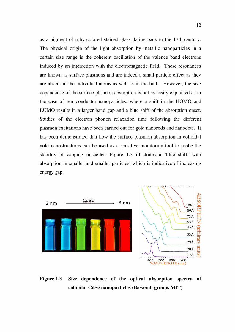
12
as a pigment of ruby-colored stained glass dating back to the 17th century.
The physical origin of the light absorption by metallic nanoparticles in a
certain size range is the coherent oscillation of the valence band electrons
induced by an interaction with the electromagnetic field. These resonances
are known as surface plasmons and are indeed a small particle effect as they
are absent in the individual atoms as well as in the bulk. However, the size
dependence of the surface plasmon absorption is not as easily explained as in
the case of semiconductor nanoparticles, where a shift in the HOMO and
LUMO results in a larger band gap and a blue shift of the absorption onset.
Studies of the electron phonon relaxation time following the different
plasmon excitations have been carried out for gold nanorods and nanodots. It
has been demonstrated that how the surface plasmon absorption in colloidal
gold nanostructures can be used as a sensitive monitoring tool to probe the
stability of capping miscelles. Figure 1.3 illustrates a ‘blue shift’ with
absorption in smaller and smaller particles, which is indicative of increasing
energy gap.
Figure 1.3 Size dependence of the optical absorption spectra of
colloidal CdSe nanoparticles (Bawendi groups MIT)

13
1.4.4.2 Luminescence properties
Luminescence may be defined as the emission of light from certain
substance, when excited with radiations like X-ray/UV/electrons and
mechanical stress/chemical reaction/electric discharge/thermal heating etc.
The emitted radiation from a luminescent material is free from heating effect
and hence is also called as ‘cold emission’. Optical excitation of
semiconductor nanoparticles often leads to both band-edge and deep trap
luminescence. The size dependence of the excitonic or band-edge
fluorescence has been studied extensively and can be reasonably explained by
the effective-mass approximation. The fluorescence process in semiconductor
nanoparticles is very complex and most nanoparticles exhibit broad and
Stokes-shifted luminescence arising from the deep traps of surface states.
Only clusters with good surface passivation show high band-edge emission.
The absence of band-edge emission has been previously attributed to the large
non-radiative decay rate of the free electrons trapped in these deep trapped
states. As the particles become smaller, the surface/volume ratio and hence
the number of surface states increases rapidly, reducing the excitonic
emission. Thus, surface states often determine the physical properties,
especially the optical properties of nanoparticles.
Photoluminescence is classified into two types, depending upon the
nature of the ground and the excited states. In a singlet excited state, the
electron in the higher energy orbital has the opposite spin orientation as the
second electron in the lower orbital. These two electrons are said to be paired.
In a triplet state these electrons are unpaired, that is, their spins have the same
orientation. Returning to the ground state from an excited singlet state does
not require an electron to change its spin orientation. A change of spin
orientation is needed for a triplet state to return to the singlet ground state
(Figure 1.4).

14
Fluorescence is the emission which results from the return to the
lower orbital of the paired electron. Such transitions are quantum
mechanically, “allowed” and the emissive rates are typically near 108 s
1.
These high emissive rates result in fluorescence lifetimes near 108 s or 10 ns.
The lifetime is the average period of time a fluorophore remains in the excited
state. Phosphorescence is the emission which results from transition between
states of different multiplicity, generally a triplet excited state returning to a
singlet ground state. Such transitions are not allowed and the emissive rates
are slow. Typical phosphorescent lifetimes range from milliseconds to
seconds, depending primarily upon the importance of deactivation processes
other than emission.
Figure 1.4 Fluorescence and phosphorescence mechanism

15
1.4.5 Electrical and Electronic Properties
The electrical conductivity of the solids is determined by its
electronic structure or band structure. A crystalline solid is called a metal if
the uppermost energy band is partly filled or the uppermost filled band and
the next unoccupied band overlap in energy. In the case of semiconductors,
the completely filled valance band and the empty conduction band are
separated by an energy gap (Eg) which is small ( 3 eV). The electrons can be
excited from the valence band to conduction band using light or heat, which
results in partial conductivity. In insulator, the Eg is high and the electrical
conductivity is restricted. The conducting nature of the solids can be affected
by various factors like, temperature and particle size. When the particle size
is reduced to nanometer range, the Eg increases and hence the conductivity is
reduced. In the case of metal nanoparticles, the density of states in the
conduction and valence bands are reduced and electronic properties changed
drastically i.e., the quasi-continuous density of states is replaced by quantized
levels with a size dependent spacing, in this situation, the metal does not
exhibit bulk metallic or semiconducting behaviour.
The size quantization effect may be regarded as the onset of the
metal to non-metal transition. The size at which transition occurs depends on
the nature of the metal. Because of the increased volume fraction of atoms
lying at the grain boundaries, the electrical resistivity of nanocrystalline
materials, as affected by grain boundary scattering, is found to be higher than
that in the coarse-grained material of the chemical composition. It has also
been shown that the electrical resistivity of nanocrystalline materials is
sensitive not only to the grain boundaries but also to other types of
imperfections and/or stresses introduced by the synthesis process. At a
constant temperature, the electrical resistivity increases with a decrease in
grain size and for a constant grain size, the electrical resistivity increases with

16
temperature and both these observations are consistent with the theoretical
analysis of scattering of electrons by grain boundaries. The magnitude of the
electrical resistivity (and hence conductivity) in nanocomposites can be
changed by altering the grain size. For example, by changing the volume
fraction of iron particles in a nanocrystalline iron–silica system, the electrical
conductivity could be changed by 14 orders of magnitude.
1.4.6 Magnetic Properties
Many properties of magnetic systems are fundamentally determined
by the underlying electronic structure. Magnetic behaviour, electronic
transport and even structural stability are intimately related to electronic
properties. Reducing the size or dimension of magnetic systems changes the
electronic properties by reducing the symmetry of the system and by
introducing a quantum confinement, the strength of a magnet in terms of
coercivity and saturation magnetization value. These values increase with
decrease in the grain size and an increase in the specific area (surface per unit
volume) of the grains.
Nanoparticles exhibit magnetic properties that are different from
bulk materials. These are due to the following reasons: (i) As the grain size of
these systems reaches the typical lengths of few nanometers, the response of
the system depends on the boundary conditions (which are no longer periodic,
but determined by the particle size) and therefore, to be different from bulk
material. (ii) Because of the large ratio of surface to volume atoms in
nanoparticles, the surface energy becomes important when compared with
volume energy and therefore, the equilibrium situation can be different that
for bulk materials. The energy barrier to overcome for magnetization
inversion is KV, where K is the anisotropy constant and V the particle
volume. In the case of nanoparticles, the volume is so small, therefore the
thermal energy (KBT) is enough to invert the magnetization with relaxation

17
time as low as few seconds. Thus, the material loses coercivity and
remanence, giving rise to the so-called super paramagnetic behaviour. It is
found that the changes in the interatomic distances have a strong influence on
the magnetic properties. The saturation magnetization M and curie transition
temperature of nanocrystalline materials are considerably varied with respect
to the bulk materials.
The coercivity of the fine particles increases as the particle size is
reduced. The increase in coercivity attains a maximum and then tends to zero.
In certain solid solutions, there may be small clusters containing more than
the average number of magnetic ions, surrounded by non-magnetic ions.
These magnetic clusters within the solid solution act as super paramagnetic in
nature.
1.5 APPLICATIONS OF NANOMATERIALS
Nanomaterials offer an extremely broad range of potential
applications from electronics, optical communications and biological systems
to new materials. Many possible applications have been explored and many
devices and systems have been studied. More potential applications and new
devices are being proposed in literature. It is obviously impossible to
summarize all the devices and applications that have been studied and it is
impossible to predict new applications and devices. It is interesting to note
that the applications of nanotechnology in different fields have distinctly
different demands and thus face very different challenges, which require
different approaches.
Applications of nanostructures and nanomaterials are based on (i)
the peculiar physical properties of nanosized materials, e.g. gold nanoparticles
used as inorganic dye to introduce colors into glass and as low temperature
catalyst, (ii) the huge surface area, such as mesoporous titania for photo

18
electrochemical cells and nanoparticles for various sensors and (iii) the small
size that offers extra possibilities for manipulation and room for
accommodating multiple functionalities. For many applications, new
materials and new properties are introduced. For example, various organic
molecules are incorporated into electronic devices, such as sensors (Briseno
and Yang 2009; Star et al 2003). One important branch of nanotechnology is
nanobiotechnology. Nanobiotechnology includes; (i) the use of nanostructures
as highly sophisticated scopes, machines or materials in biology and/or
medicine and (ii) the use of biological molecules to assemble nanoscale
structure (Parak et al 2003).
The II-VI semiconductor nanostructures represent ideal systems for
dimension-dependent properties and are expected to play an important role as
building blocks in devices and processes, such as light emitting diodes, solar
cells, single electron transistors, lasers and biological labels (Deka et al 2009;
Friedman et al 2005; Grimsdale et al 2009; Kamat 2008). Semiconductor
nanoparticles are successfully utilized in photocatalytic applications.
Colloidal semiconductors were first introduced in 1976. Since then, the
promising application of nanoparticles in photocatalysis has achieved great
attention and been extensively investigated (Palmisano et al 2007). The
semiconductor catalysts form a heterogeneous photocatalysis system with
pollutant molecules and exhibit high degradation effectiveness. The design of
highly efficient and selective photocatalytic systems that can work in the
reduction of global air and water pollution is of vital interest. Especially, the
modified WO3 and CdS semiconductors are well known as photocatalysts that
can operate under visible light, even though they are not stable and have small
reactivity (Kim et al 2011). On the other hand, sensitization using dye
molecules loaded on semiconductor photocatalysts has been successfully and
widely applied to utilize solar energy. Although this dye-sensitized system

19
has been developed to be utilized as a Graetzel cell, which can convert solar
energy to electronic energy efficiently and directly, the dye molecules are not
stable when this system is applied as a photocatalysts under environmental
conditions (Grätzel 2003; Senthilnathan and Ganesan 2010).
1.6 II-VI SEMICONDUCTOR NANOPARTICLES
Over the past two decades, there have been extensive experimental
and theoretical studies of optical responses of semiconductor nanoparticles,
because they have a wealth of quantum phenomena and show unique size-
dependent materials properties. In particular, there are two active research
fields in semiconductor nanoparticles optics: indirect-gap group IV
semiconductor nanoparticles and II–VI compound semiconductor
nanoparticles. The electronic and optical properties of II-VI compound
semiconductor nanoparticles have been extensively investigated in view of a
wide variety of applications. With change in the particle size, dramatic
modifications of their electronic and optical properties take place due to the
three-dimensional quantum confinement of electrons and holes when the size
of the particle approaches the Bohr radius of an exciton (Kukushkin et al
2011; Yadav et al 2010). In addition to the change in electronic and optical
properties, the structural behavior also exhibits changes with change in
particle size. Semiconductors with widely tunable energy band gap are
considered to be the materials for next generation flat panel displays,
photovoltaic, optoelectronic devices, laser, sensors, photonic band gap
devices, etc.
Artificially obtained semiconductor structures with reduced
dimensions present a large variety of new interesting properties in comparison
to the bulk material and open new ways in the engineering of semiconductors.
By simple combination of two semiconductor materials of different band gap

20
energies a spatial confinement of carrier motion in the direction of the growth
axis is obtained. Further, the decrease of dimensions to one-dimensional and
quasi-zero dimensional structures leads to large enhancement of their optical
properties. Confinement of carriers in all 3 spatial directions consequently
involves a redistribution of the energy in well-like energy levels. Moreover,
quantum dots are known as prototypes in the physics of quantum
confinement. A brief review of the basic properties of II-VI semiconductor
nanocrystals are dealt with in this chapter.
In industry, the most frequently used II-VI semiconductor
nanostructures are cadmium and zinc chalchogenides. Cadmium sulphide is
yellow in color and is a chemical compound with the chemical formula CdS.
It is a direct band gap semiconductor (2.42 eV) and has many applications.
Cadmium sulphide has, like zinc sulphide, two crystal forms: the more stable
hexagonal wurtzite structure (found in the mineral Greenockite) and the cubic
zinc blende structure (found in the mineral Hawleyite). The wurtzite
(hexagonal) structure is stable from room temperature to melting point.
However, metastable cubic phase has been found in thin films and
nanocrystalline powders (Murray et al 1993; Wang et al 2002). The two types
of structures are illustrated schematically in Figure 1.5. Both wurtzite and zinc
blend structures show tetrahedral coordination, i.e. each cation is surrounded
by 4 anions and vice versa. The bulk material usually crystallizes in wurtzite
structure, whereas in the case of nanocrystals these two structures coexist.
Their ratio can be controlled through appropriate selection (control of
temperature) of growth conditions. Another important parameter for the
characterization of the crystallographic structure of II-VI quantum dots is the
lattice constant. Table 1.2 contains information about the lattice constants of
the two structures for the most commonly used bulk semiconductors.

21
Hexagonal Cubic
Figure 1.5 The crystallographic structures of II-VI semiconductors.
Black spheres are cations (and can be Zn, Cd or Hg atoms),
whereas white spheres are anions S, Se or Te atoms.
Table 1.2 The lattice constant a in Å of II-VI semiconductors and the
numerical values in brackets indicate the lattice constant of
the metastable structure
CompoundsHexagonal
(Wurtzite)
Cubic
(Zinc Blend)
ZnSe (4.01) 5.669
CdS 4.137 (5.838)
CdSe 4.298 (6.084)
CdTe (4.57) 6.481
The crystallographic structure of mixed semiconductor nanocrystals
i.e., CdSxSe1-x is also determined by the preparation conditions, depending on
the (stable) crystallographic structure of the compounds CdS and CdSe.

22
1.7 DOPED II-VI SEMICONDUCTOR NANOPARTICLES
Doping is very important not only to control the transport
properties of the semiconductors but also to modify their optical properties.
Hence, they find applications in display screens of computer monitors,
screens of cathode ray tubes (CRT), fluorescent lamps, X-ray detectors, light
emitting diodes (LED), laser materials, etc. Semiconductors used in such
applications are doped with metal ions, especially transition, or rare earth
metal ions. Sometimes, additional metal ions are used as co-activators to
enhance the emission. Doped semiconductors have been widely investigated
in the past. Depending upon the size and charge on the ion, substitutional
doping of impurity ions can produce either excess electrons or holes in a
semiconductor or just lattice distortion can take place. This gives rise to
localized levels in the band gap of a semiconductor. Such states are
responsible for transport properties, photo luminescence, electro
luminescence and other optical properties in these semiconductors.
In the doped nanoparticles, the number of doped atoms therefore
should be still smaller, that is, just a few atoms per particle. The alteration of
electronic structure, the optical and other properties, of doped semiconductor
nanoparticles, is an interesting area of nanoparticles research. There are
attempts not only to investigate the static equilibrium properties of the doped
nanoparticles but also the charge dynamics in nanoparticles. The first report
on the doped nanoparticles appeared in 1983 (Becker and Bard 1983).
However, it was an unintentional synthesis of nanoparticles. Wang et al
(1991) reported the results of their work on clusters. Bhargava et al (1994)
reported a large enhancement of photoluminescence in Mn-doped ZnS
nanoparticles. They further stressed that doped nanoparticles form a new class
of materials in which photoluminescence efficiency increases and decay time
reduces dramatically by some orders of magnitude. Following this report,

23
many groups made investigations on doped semiconductor particles of
various sizes as well as materials. Synthesis of doped nanoparticles by various
commonly used methods is discussed in chapter 2.
1.7.1 Doped CdS Nanoparticles
Metal sulfides CdS, ZnS, CdxZn1-xS and CdxMn1-xS are
technologically important materials which have been used in the form of thin
films for a variety of applications including optical coatings, solid-state solar
cell windows, electro optic modulators, photoconductors, field effect
transistors, sensors and transducers. The impurity ions were doped into the
inorganic core of the CdS nanostructures, various factors such as mismatch in
the ionic radius, charge imbalance, different coordination, as well as
differences in chemical properties between the Cd2+
, Zn2+
and Mn2+
metal
ions are observed. A great deal of attention has been paid to doped
semiconductor nanostructures with magnetic ions such as Mn2+
, Cr2+
, Fe2+
and Co2+
to impart the unusual giant Zeeman, Faraday rotation and magnetic
polaron effects that characterize this class of materials, known as diluted
magnetic semiconductors (DMS).
1.7.1.1 CdS: Zn Nanoparticles
CdS is structurally very similar to ZnS and belongs to the same
II–VI group of semiconductors. Bulk CdS has a large and direct band gap of
2.42 and 2.56 eV at 300 and 0 K, respectively. Cd xZnxS is a promising
material for optoelectronic applications in the blue and UV spectral region
due to its wide direct bandgap and a lattice constant which can be matched to
common substrates such as GaAs, GaP or Si (Bailey and Nie 2003; Li et al
2005). Cd1-xZnxS in bulk form has a band gap which is tunable from 2.4 to
3.7 eV and, hence, can emit at different wavelengths (different band-to-band
transitions) by varying the x values from 0 to 1. In solar cell systems, where

24
CdS films have been demonstrated to be effective, the replacement of CdS
with the higher band gap Cd1-xZnxS alloys has led to a decrease in window
absorption losses and an increase in the short circuit current ( Gaewdang and
Gaewdang 2005).
A Cd1-xZnxS alloy has higher efficiency than those of pure CdS and
ZnS as photocatalysts in hydrogen production. CdS alone, however, shows
negligible photocatalytic activity because of its instability and rapid electron-
hole pair recombination rates. Studies have proven that with the appropriate
particle interaction, CdxZn1-xS nanoparticles can efficiently decompose
organics such as phenol and methylene blue under visible light irradiation.
Moreover, the optical properties of Cd1-xZnxS can likewise be
effectively tuned through control of its phase, morphology and size; for
example, more efficient luminescence has already been achieved in ternary
Cd1-xZnxS, as well as in binary ZnS and CdS nanoparticles, in comparison
with their bulk counterparts (Chen and Gao 2005; Liu et al 2005; Villoria et al
2010; Kim et al 2007; Zhang et al 2007). The tunability of the optical
properties of Cd1-xZnxS relative to its composition, in addition to its phase,
morphology and size, should make it a more interesting material to study,
considering the excitement of understanding new science and the potential
hope for novel applications and even economic impacts. Unfortunately, to our
knowledge, the literature reporting the synthesis and characterization of
Cd1-xZnxS (0 < x < 1) nanostructures is limited so far.
1.7.1.2 CdS: Mn Nanoparticles
Magnetic semiconductors are key materials for device ideas in
quantum computing and spin electronics. The 2+ magnetic ions are easily
incorporated into the host II-VI crystals by replacing group II cations. In such
II-VI based DMS such as (CdMn) Se, magneto-optical properties were
25
extensively studied and optical isolators were fabricated using their large
faraday effect (Tanaka 1998). Although this phenomenon makes these DMS
relatively easy to prepare in bulk form as well as thin epitaxial layers, II-VI
based DMS are difficult to dope to create p- and n-type, which makes the
material less attractive for electro optic applications.
In II-VI DMS, crystallizing in zinc blende/wurtzite structure the
‘d-d’ and ‘sp-d’ exchange interactions play an important role. The ‘sp-d’
exchange interaction influences the transport properties, while the ‘d-d’
exchange interaction controls the static and dynamic magnetic properties of
DMS. The exchange integrals have been reported from different experiments
like high field magnetization, neutron scattering, Raman Scattering and
susceptibility measurements. Larson et al (1988) calculated Jdd using
perturbation technique and showed that it has three contributions arising from
super exchange, the Bloebergen-Rowland process and Ruderman-Kittel-
Kasuya-Yosida (RKKY) like process between conduction electrons. The
dominant contribution comes from the hybridization induced super exchange
interaction involving only anion derived upper valence band states and the
Mn ‘d’-states. ‘sp-d’ exchange interaction is described by the super exchange
constants and arising respectively from the electron or hole interactions
with the ‘d’ electrons at the center of the Brilliouin zone. These super
exchange contributions aid ferro and antiferromagnetic orderings respectively.
Due to the higher value of , II-VI based DMS are antiferromagnetic in
nature, whereas in Cr based II-VI DMS, with larger values are
ferromagnetic.
1.8 II-VI SEMICONDUCTOR PHOTOCATALYSTS
In recent years, interest has been focused on the use of
semiconductor materials as photocatalysts for the removal of organic and

26
inorganic species from aqueous or gas phase. This method has been suggested
in environmental protection due to its ability to oxidise the organic and
inorganic substrates. In heterogeneous photocatalysis two or more phases are
used in the photocatalytic reaction. The semiconductor photocatalysts have
large band gap (Eg > 2.2 eV). Size dependent band gap expansion is helpful in
development of photocatalytic properties in nanocrystals of semiconductors.
A combined effect of size dependent band edge potential growth and the
photo induced polarization of semiconductor nanocrystals determine their
photocatalytic properties. A light source with semiconductor material is used
to initiate the photoreaction. The catalysts can carry out substrate oxidations
and reductions simultaneously. UV light of long wavelengths can be used,
possibly even sunlight.
Semiconductor photocatalysis with a primary focus on TiO2 as a
durable photocatalyst has been applied to a variety of problems of
environmental interest in addition to water and air purification. Several
semiconductors such as ZnO, ZnS, CdS, TiO2 and Fe2O3 have been used for
heterogeneous photocatalytic destruction of organic pollutants in waste water
(Chen et al 2010, Xiong et al 2010). Dyes are the important class of organic
water pollutants and therefore, many studies have been conducted on the
photodegradation. Among these photocatalysts, nanosized CdS is an
interesting photocatalyst material, since it has a narrow band gap (2.4 eV) and
a suitable conduction band potential for photocatalysis. Incorporation of
elements in the structure of CdS making solid solutions is a powerful strategy
for improving the photocatalytic properties of CdS. The solid solution
photocatalysts have advantages compared to doped photocatalysts since solid
solution allows one to control the potentials of the conduction and valence
bands, and the photogenerated electrons and holes are able to move in the
continuous valence and conduction bands instead of the discrete donor levels
seen in the doped photocatalysts (Villoria et al 2010). The photocatalytic

27
properties of synthesized CdS nanoparticles for the degradation of Rhodamine
B under UV irradiation have been studied and discussed in chapter 4.
1.9 AIM OF THE PRESENT WORK
In view of the above importances, the present work is focused on
the synthesis and property studies of pure and doped CdS nanostructures. The
structural and optical properties of the nanoparticles were studied and the
results are presented in the thesis. Specifically, the present work concerns the
following objectives:
To synthesize the molecular precursors Metal-pyrrolidine
dithiocarbamate complexes by chemical precipitation
technique.
To synthesize pure, Zn and Mn doped CdS nanoparticles by
thermal decomposition of Metal complexes by conventional
and microwave heating.
To study the structural and optical properties of synthesized
nanoparticles using different characterization techniques.
To compare the properties of the nanoparticles obtained from
both conventional and microwave heating processes.
To study the photocatalytic activities of these nanoparticles by
photo degradation of Rhodamine B dye under UV irradiation.