Chapter 1 Introduction 1.1 Motivation · The maximum oscillation frequency ... MOSFETs is...
62
1 Chapter 1 Introduction 1.1 Motivation The rapid technology evolution of Si MOSFET is beneficial for IC design with higher device speed and cost reduction. Besides the advantages on digital performance, the scaling of CMOS technology has largely improved the RF performance of MOS devices. The most significant improvement along with CMOS technology scaling is the larger RF gain, higher cut-off frequency (f t ) and maximum oscillation frequency (f max ) [1]-[11]. This has made CMOS device technology the prime choice for Mixed-Signal/RF system-on-chip (SoC) application such as WCDMA, W-LAN, and Ultra-Wide Band (UWB) wireless communication. The single chip radio design requires integration of high-performance analog components for base-band signal processing, high-performance RF transistors and passive components for low noise amplifiers and mixers, and high voltage components for power management. These elements are necessary to realize a single-chip RF transceiver design. Among the passive components for mixed-signal and radio-frequency design application, Metal-Insulator-Metal (MiM) capacitors are the most important passive components. The process design of MiM materials and structures is much more difficult after Cu was introduced into the BEOL process technology. The choice of MiM materials will significantly influence the performance of MiM capacitors. We have therefore compared the performance and process complexity by using different materials as the electro-plates and insulator dielectric of the MiM capacitors. The process issues while integrating the MiM capacitor into the Cu BEOL are also discussed. Our results showed that the MiM performance can be optimized by properly optimizing the MiM process
Transcript of Chapter 1 Introduction 1.1 Motivation · The maximum oscillation frequency ... MOSFETs is...
1
Chapter 1
Introduction
1.1 Motivation
The rapid technology evolution of Si MOSFET is beneficial for IC design with
higher device speed and cost reduction. Besides the advantages on digital performance, the
scaling of CMOS technology has largely improved the RF performance of MOS devices.
The most significant improvement along with CMOS technology scaling is the larger RF
gain, higher cut-off frequency (ft) and maximum oscillation frequency (fmax) [1]-[11]. This
has made CMOS device technology the prime choice for Mixed-Signal/RF system-on-chip
(SoC) application such as WCDMA, W-LAN, and Ultra-Wide Band (UWB) wireless
communication. The single chip radio design requires integration of high-performance
analog components for base-band signal processing, high-performance RF transistors and
passive components for low noise amplifiers and mixers, and high voltage components for
power management. These elements are necessary to realize a single-chip RF transceiver
design.
Among the passive components for mixed-signal and radio-frequency design
application, Metal-Insulator-Metal (MiM) capacitors are the most important passive
components. The process design of MiM materials and structures is much more difficult
after Cu was introduced into the BEOL process technology. The choice of MiM materials
will significantly influence the performance of MiM capacitors. We have therefore
compared the performance and process complexity by using different materials as the
electro-plates and insulator dielectric of the MiM capacitors. The process issues while
integrating the MiM capacitor into the Cu BEOL are also discussed. Our results showed
that the MiM performance can be optimized by properly optimizing the MiM process
2
conditions to achieve both high performance and reliable MiM capacitor integrated in the
Cu BEOL.
The scaling on CMOS technology has improved device speed and reduced cost
per transistor. The maximum oscillation frequency (fmax) is also improved larger than 40
GHz for 0.18 μm technology node [1]. The implementation of Cu interconnect in 0.13 μm
technology significantly reduces the wire resistance and improves the quality factor of
passive components. However, the low drain breakdown voltage of CMOS transistors
limits the usage of CMOS for power amplifiers. This limitation for high voltage operation
significantly reduces the maximum output power and efficiency for CMOS devices.
Therefore, the RF SoC design, which includes the RF power amplifier, is a long time
historical challenge for using the baseline CMOS logic process. In the past, the LDMOS
transistors were introduced to overcome the low drain break-down voltage issue at the
expense of complex process and lower operation speed [12]-[14]. However, this is
opposite to the technology trend for wireless communication, where continuously
increasing operation frequency is needed. To overcome the low breakdown voltage issue
and improve the RF power performance, we designed an asymmetric lightly-doped-drain
(LDD) MOS transistor for high frequency RF power application. This new
asymmetric-LDD MOS transistor is fully embedded in the conventional foundry logic
process without any additional process step or extra cost. The drain breakdown voltage at
Vgs=0 V (BVdss) is increased from 3.6 V in conventional transistor to 7.0 V in this new
asymmetric-LDD device for the same 0.23 μm gate length. By properly increasing the
drain operation point at 2.5 V for the new asymmetric-LDD MOS transistor, the output
power can be increased to 38% at 2.4 GHz under peak power-added efficiency (PAE)
condition.
The efforts to integrate high-quality MiM capacitor into Cu-BEOL and design a
3
new high-efficiency power MOSFET for low-voltage power amplifier application is a step
further to realize the MS/RF SoC design.
1.2 Outline of the Dissertation
The single chip transceiver design requires integration of high-performance
analog components for base-band signal processing, high-performance RF transistors and
passive components for low noise amplifiers and mixers, and high voltage components for
power management. In my research, it includes three parts to cover the importance topics
on realizing the RF-SoC design in Si-MOS process technology. The first part is RF noise
optimization and modeling. The research is to provide guidance for performance
optimization on LNA design. The second part is MiM integration with Cu-BEOL process.
This is to discuss the issues of this key passive component while being integrated into
Cu-BEOL process for analog/mixed-signal design. The third part is the improvement of
RF power performance on Si-MOS transistor by a new device structure. This part is to
address the difficult topic of integrating Si-MOS power amplifier into RF-SoC design.
Therefore, my research is to discuss the device and process issues we faced while realizing
a single-chip transceiver design.
In this dissertation, we started with the introduction of basic RF parameter
definition, power measurement method, and RF noise optimization and modeling for RF
system in Chapter 2.
In Chapter 3, we discussed the process design consideration and performance
comparison of different materials as the bottom electro-plat of MiM capacitors. The
difficulty of integrating the MiM capacitor into the Cu BEOL is also discussed. We have
also discussed how to improve the breakdown voltage (Vbd) failure of the MiM capacitor.
Different insulator dielectrics have different electrical characteristics. We have compared
4
the electrical characteristics of MiM capacitors by using Si3N4 and SiO2 dielectrics as the
insulator dielectrics.
In Chapter 4, we introduce a new asymmetric-LDD MOSFET for low-voltage
power amplifier application with high speed. The asymmetric-LDD MOSFET is a new
design which is fully-embedded in the conventional logic process without any added
process step and cost. The device design, layout, and how to realize this new
asymmetric-LDD transistor is explained. We have also compared the DC and RF power
performance between the conventional MOSFET and the new asymmetric-LDD transistor.
We conclude our research results in Chapter 5. The opportunities and future
works are also discussed.
5
Chapter 2
Basic Parameter Definition and RF Noise
This chapter introduces the definition of important RF parameters and RF noise.
RF noise is important for low-noise-amplifier (LNA) since the noise from the MOSFET of
first stage LNA will dominate the noise floor of the whole communication system. We
have studied how to optimize RF performance by properly select finger width and finger
number at a fixed total finger width. The accurate RF noise modeling of the nm-scale
MOSFETs is challenging due to the limited understanding of noise sources and the large
parasitic effect from low resistivity Si substrate. We have established an equivalent circuit
model with intrinsic BSIM3 model, connected gate resistance, through transmission lines
and probing pads to get the intrinsic RF noise of MOS device.
2.1 Basic RF Parameters
The basic RF parameters to be discussed in this dissertation include Q-factor,
cut-off frequency (ft), maximum oscillation frequency (fmax), and Power-Added-Effiency
(PAE).
The quality factor (Q-factor) for a system under sinusoidal excitation at a
frequency ω can be defined by the following equation [15]
dissipatedpower averagestoredenergy ω≡Q (2.1)
For a parallel RLC network at resonance, RCQ 0ω= where 0ω is the resonant
frequency of the RLC network.
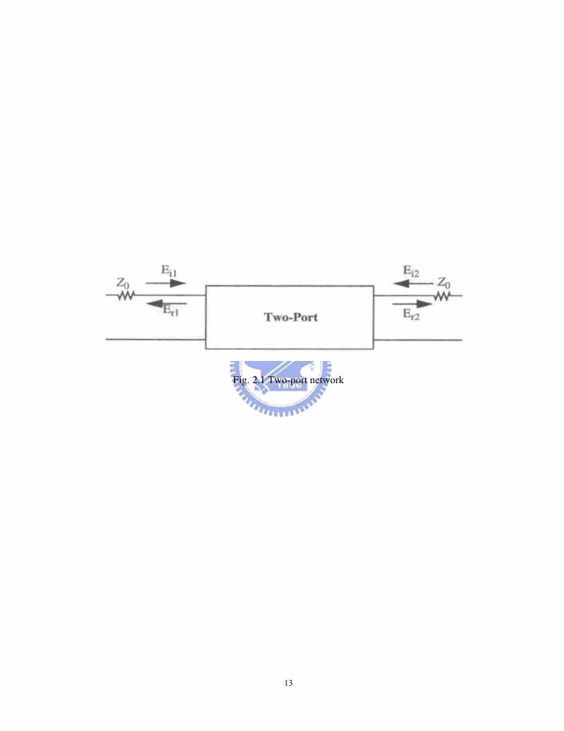
At radio-frequency range, a two-port network can be adequately characterized
by the scattering parameters (S-parameters). The S-parameters exploit the fact that a line
6
terminated in its characteristic impedance gives rise to no reflections. Scattering
parameters define the input and output variables in terms of incident and scattered voltage
waves. Figure 2.1 illustrates a two-port network wit the definitions of S-parameter port
variables. The source and load terminations are Z0. The two-port relations may be written
as
2121111 asasb += (2.2)
2221212 asasb += (2.3)
where
011 / ZEa i= (2.4)
022 / ZEa i= (2.5)
011 / ZEb r= (2.6)
022 / ZEb r= (2.7)
The short-circuit current gain (H21) and the maximum available gain (MAG) can be
calculated by the following equations [16]
21122211
2121 )1)(1( SSSS
SH++−
−= (2.8)
12
12
21 −−= kSSkMAG (2.9)
where k is the stability factor and defined by
2112
221122211
222
211
21
SSSSSSSS
k−+−−
= (2.10)
There are two important characteristic frequencies which indicate the high
frequency capability of the transistors. The cut-off frequency (ft) is the frequency when the
short-circuit current gain H21 of the device is equal to unity. The maximum oscillation
7
frequency fmax is defined as the frequency at which the MAG is equal to unity.
2.2 RF Power Measurement
The RF power characterization was carried out by on-wafer measurements using
an ATN load-pull system, where the input and output impedance matching conditions were
selected to optimize the output power.
The power added efficiency (PAE) of the power amplifier is used to indicate the
power drawn from the supply and is defined as
dc
inrfoutrf
PPP
PAE)( ,, −
= (2.11)
where outrfP , is the RF output power, inrfP , is the RF input power, and dcP is the total
dc power drawn from the power supply.
2.3 RF Performance Dependence on Layout
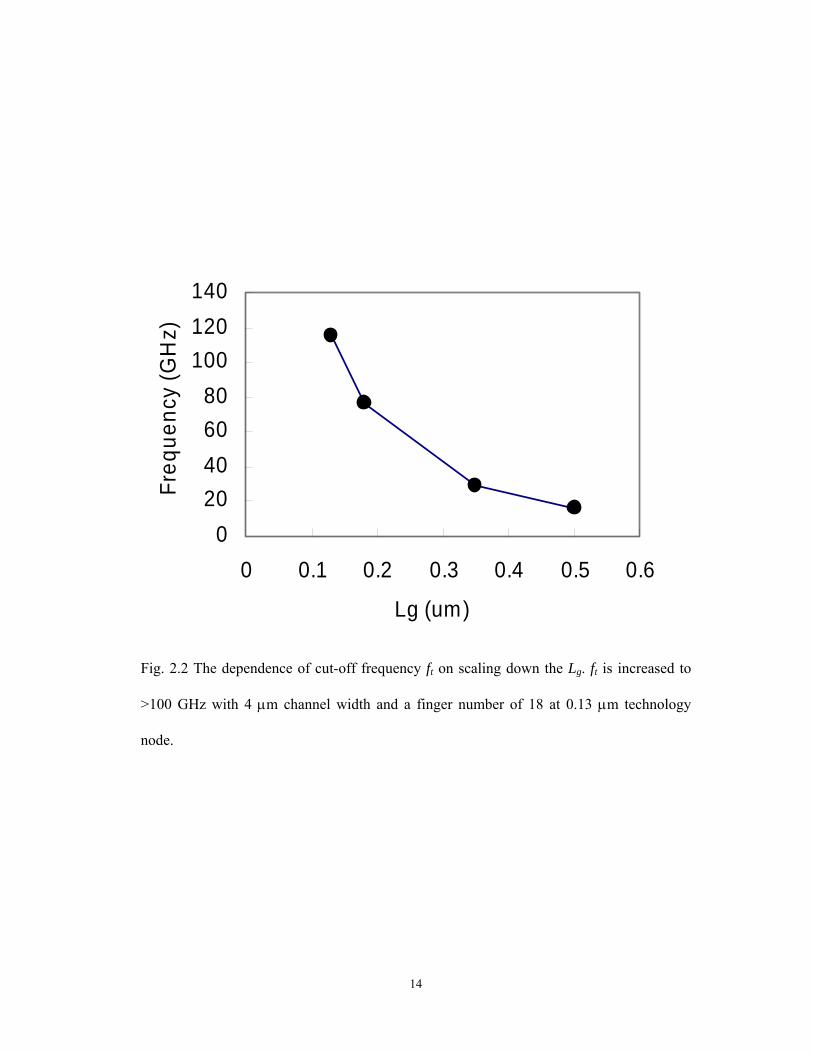
By scaling down the gate length, the unity-current-gain frequency (ft) can be
increased to ~120 GHz in 0.13 μm low-voltage logic process with 80 nm physical channel
length as shown in Fig. 2.2. The fast ft has made CMOS a popular choice for RF
system-on-chip (SoC) up to tenth GHz for wireless communication. In additional to high ft,
the RF Noise is the other important parameter to consider while scaling down the
MOSFETs. The noise from the MOSFET of first stage low-noise amplifier (LNA) will
dominate the noise floor of the whole communication system. We have studied the
dependence of minimum noise figure with finger number and finger width at a fixed total
finger width. The CMOS processes provided to designers are usually fixed and difficult for
designer to change the transistor performance. However, there is still a way for designers
8
to optimize the performance of cut-off frequency, minimum noise figure, and associated
gain based on the design requirement. By properly choosing the finger number and finger
width, the designers can still optimize the RF performance and better fit the system
requirement.
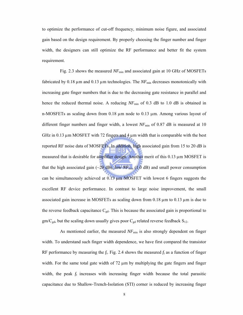
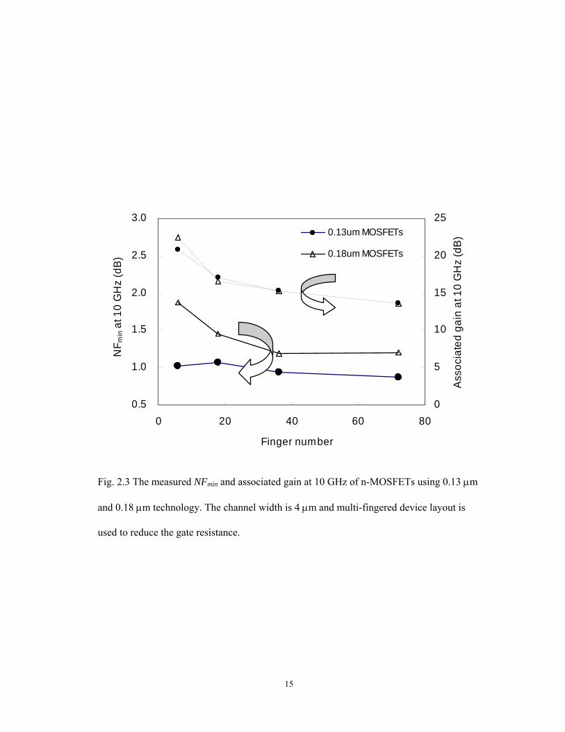
Fig. 2.3 shows the measured NFmin and associated gain at 10 GHz of MOSFETs
fabricated by 0.18 μm and 0.13 μm technologies. The NFmin decreases monotonically with
increasing gate finger numbers that is due to the decreasing gate resistance in parallel and
hence the reduced thermal noise. A reducing NFmin of 0.3 dB to 1.0 dB is obtained in
n-MOSFETs as scaling down from 0.18 μm node to 0.13 μm. Among various layout of
different finger numbers and finger width, a lowest NFmin of 0.87 dB is measured at 10
GHz in 0.13 μm MOSFET with 72 fingers and 4 μm width that is comparable with the best
reported RF noise data of MOSFETs. In addition, high associated gain from 15 to 20 dB is
measured that is desirable for amplifier design. Another merit of this 0.13 μm MOSFET is
that the high associated gain (~20 dB), low NFmin (1.0 dB) and small power consumption
can be simultaneously achieved at 0.13 μm MOSFET with lowest 6 fingers suggests the
excellent RF device performance. In contrast to large noise improvement, the small
associated gain increase in MOSFETs as scaling down from 0.18 μm to 0.13 μm is due to
the reverse feedback capacitance Cgd. This is because the associated gain is proportional to
gm/Cgd, but the scaling down usually gives poor Cgd related reverse feedback S12.
As mentioned earlier, the measured NFmin is also strongly dependent on finger
width. To understand such finger width dependence, we have first compared the transistor
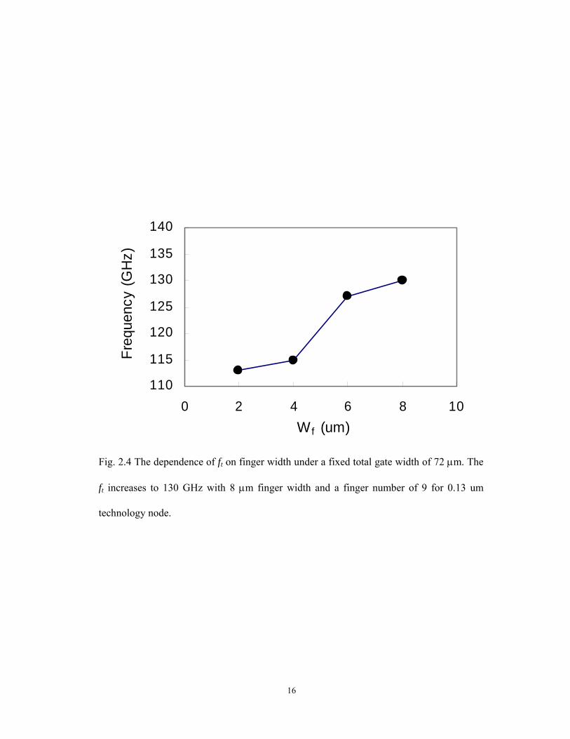
RF performance by measuring the ft. Fig. 2.4 shows the measured ft as a function of finger
width. For the same total gate width of 72 μm by multiplying the gate fingers and finger
width, the peak ft increases with increasing finger width because the total parasitic
capacitance due to Shallow-Trench-Isolation (STI) corner is reduced by increasing finger
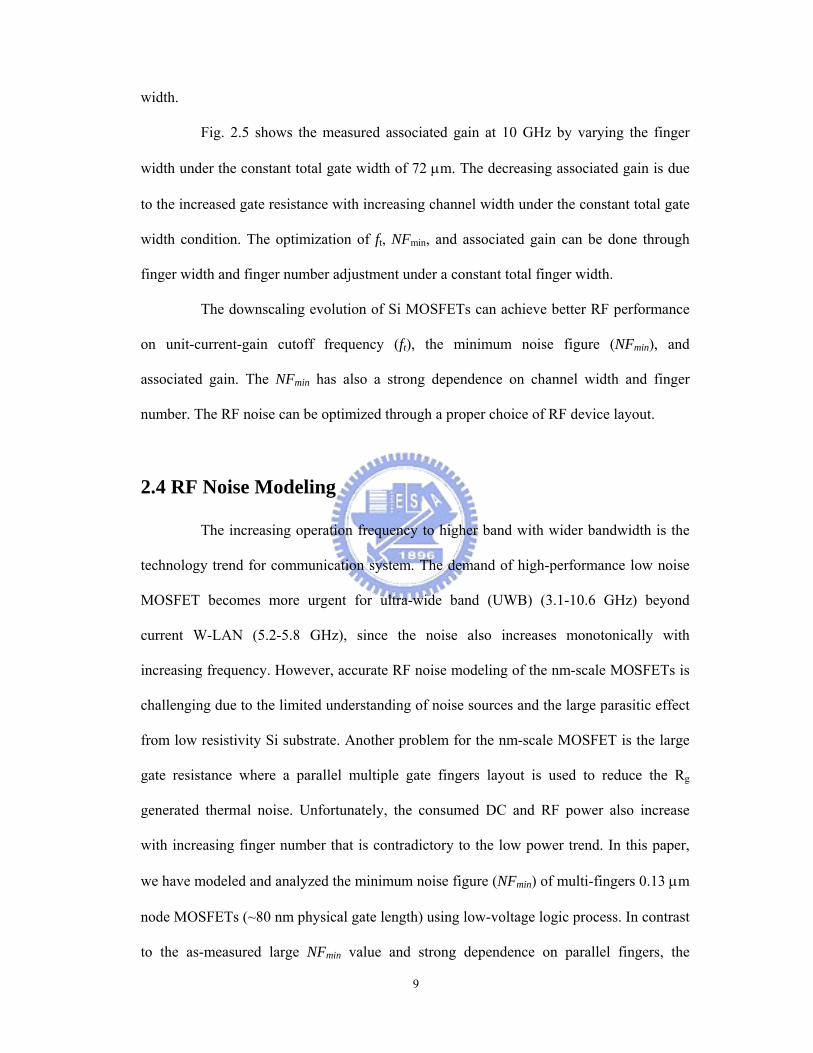
9
width.
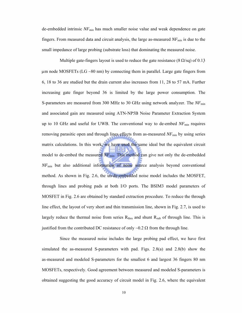
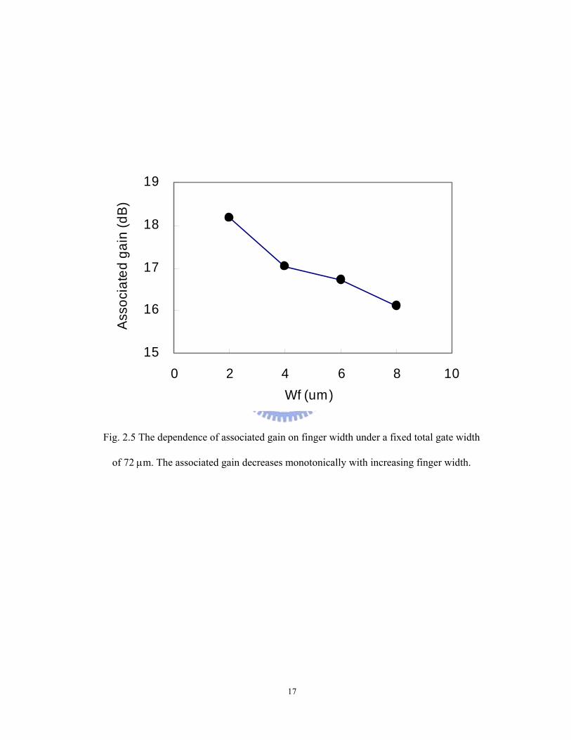
Fig. 2.5 shows the measured associated gain at 10 GHz by varying the finger
width under the constant total gate width of 72 μm. The decreasing associated gain is due
to the increased gate resistance with increasing channel width under the constant total gate
width condition. The optimization of ft, NFmin, and associated gain can be done through
finger width and finger number adjustment under a constant total finger width.
The downscaling evolution of Si MOSFETs can achieve better RF performance
on unit-current-gain cutoff frequency (ft), the minimum noise figure (NFmin), and
associated gain. The NFmin has also a strong dependence on channel width and finger
number. The RF noise can be optimized through a proper choice of RF device layout.
2.4 RF Noise Modeling
The increasing operation frequency to higher band with wider bandwidth is the
technology trend for communication system. The demand of high-performance low noise
MOSFET becomes more urgent for ultra-wide band (UWB) (3.1-10.6 GHz) beyond
current W-LAN (5.2-5.8 GHz), since the noise also increases monotonically with
increasing frequency. However, accurate RF noise modeling of the nm-scale MOSFETs is
challenging due to the limited understanding of noise sources and the large parasitic effect
from low resistivity Si substrate. Another problem for the nm-scale MOSFET is the large
gate resistance where a parallel multiple gate fingers layout is used to reduce the Rg
generated thermal noise. Unfortunately, the consumed DC and RF power also increase
with increasing finger number that is contradictory to the low power trend. In this paper,
we have modeled and analyzed the minimum noise figure (NFmin) of multi-fingers 0.13 μm
node MOSFETs (~80 nm physical gate length) using low-voltage logic process. In contrast
to the as-measured large NFmin value and strong dependence on parallel fingers, the
10
de-embedded intrinsic NFmin has much smaller noise value and weak dependence on gate
fingers. From measured data and circuit analysis, the large as-measured NFmin is due to the
small impedance of large probing (substrate loss) that dominating the measured noise.
Multiple gate-fingers layout is used to reduce the gate resistance (8 Ω/sq) of 0.13
μm node MOSFETs (LG ~80 nm) by connecting them in parallel. Large gate fingers from
6, 18 to 36 are studied but the drain current also increases from 11, 28 to 57 mA. Further
increasing gate finger beyond 36 is limited by the large power consumption. The
S-parameters are measured from 300 MHz to 30 GHz using network analyzer. The NFmin
and associated gain are measured using ATN-NP5B Noise Parameter Extraction System
up to 10 GHz and useful for UWB. The conventional way to de-embed NFmin requires
removing parasitic open and through lines effects from as-measured NFmin by using series
matrix calculations. In this work, we have used the same ideal but the equivalent circuit
model to de-embed the measured NFmin. This method can give not only the de-embedded
NFmin but also additional information of noise source analysis beyond conventional
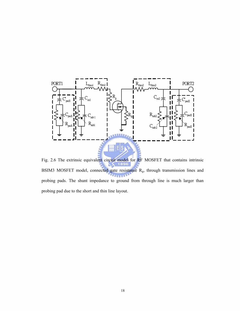
method. As shown in Fig. 2.6, the un-de-embedded noise model includes the MOSFET,
through lines and probing pads at both I/O ports. The BSIM3 model parameters of
MOSFET in Fig. 2.6 are obtained by standard extraction procedure. To reduce the through
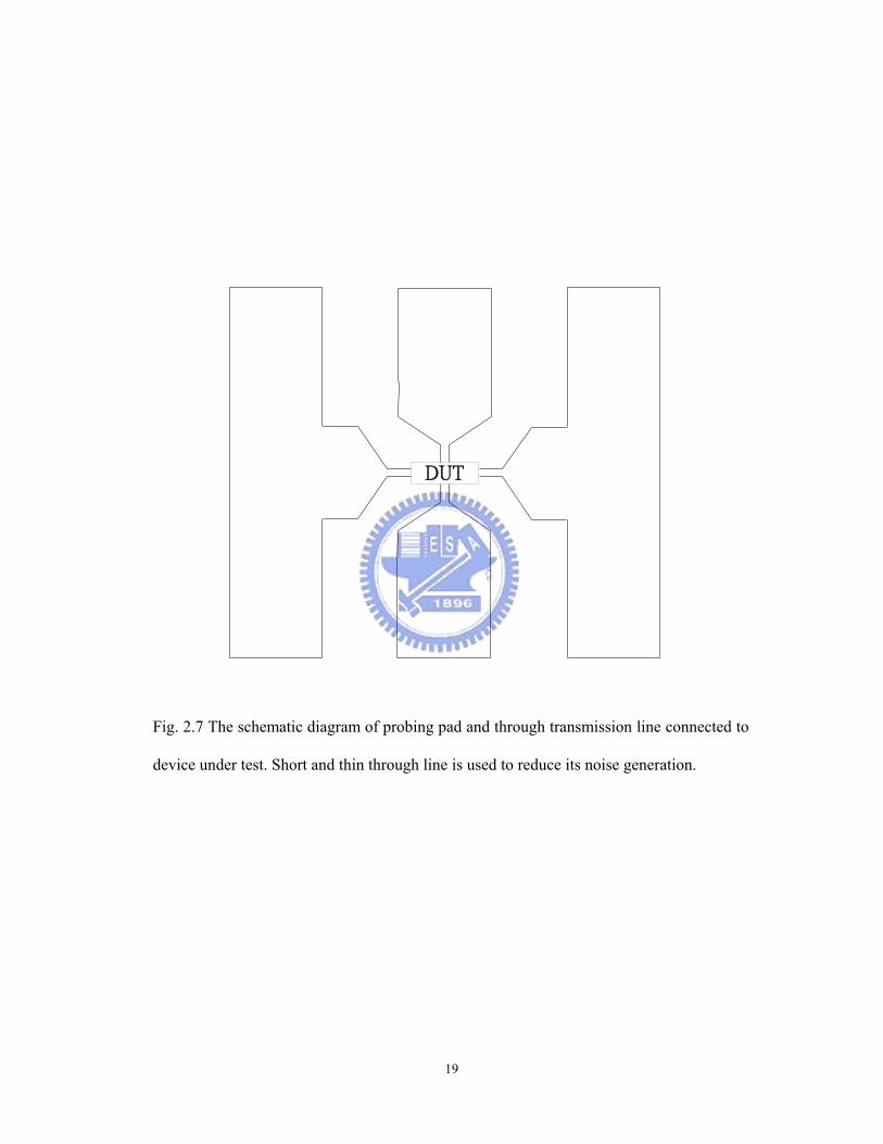
line effect, the layout of very short and thin transmission line, shown in Fig. 2.7, is used to
largely reduce the thermal noise from series Rthru and shunt Rsub of through line. This is
justified from the contributed DC resistance of only ~0.2 Ω from the through line.
Since the measured noise includes the large probing pad effect, we have first
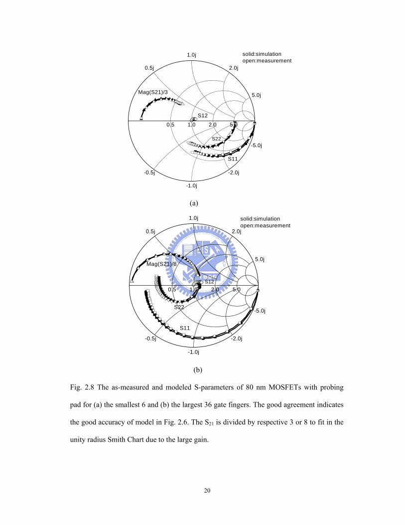
simulated the as-measured S-parameters with pad. Figs. 2.8(a) and 2.8(b) show the
as-measured and modeled S-parameters for the smallest 6 and largest 36 fingers 80 nm
MOSFETs, respectively. Good agreement between measured and modeled S-parameters is
obtained suggesting the good accuracy of circuit model in Fig. 2.6, where the equivalent
11
circuit model for open pad in I/O ports is from the well matched simulation of open pad
sub-circuit with measured S-parameters.
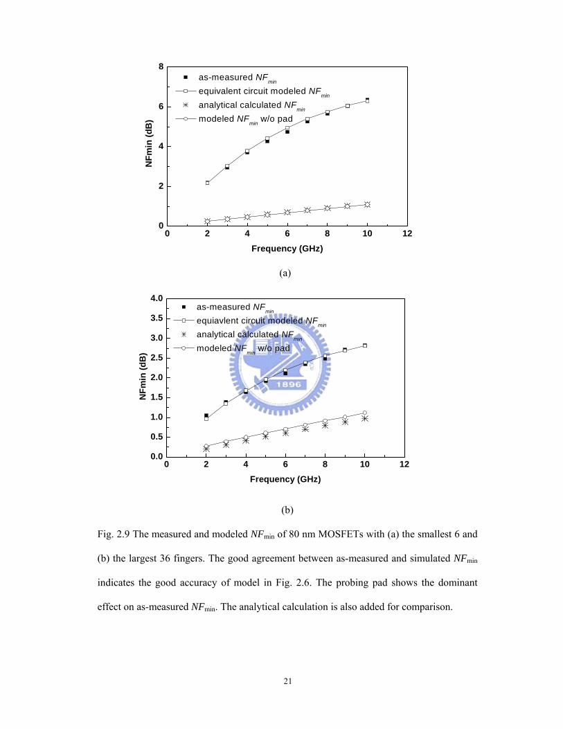
Figs. 2.9(a) and 2.9(b) show the as-measured and simulated NFmin of the smallest
6 and largest 36 fingers 80 nm MOSFETs, respectively, where the simulated data is from
the equivalent circuit model in Fig. 2.6 with extrinsic modeling parameters from the well
matched S-parameters in Fig. 2.8. The excellent agreement between as-measured and
simulated NFmin, in combining with the well matched S-parameters in Fig. 2.8, indicates
the good accuracy of circuit model in Fig. 2.6. Therefore, the same model is suitable to
provide self-consistent solutions for NFmin, S-parameters, and DC (from extracted BSIM3
modeling parameters).
We have further used the well matched equivalent circuit model to de-embed the
noise generated from the probing pad. The pad equivalent sub-circuit is included inside the
extrinsic model in Fig. 2.6 and the parameters values are obtained from the well agreed
simulation data with measured S-parameters of open pad. The de-embedded NFmin, is also
shown in Fig. 2.9, which is largely reduced from as-measured data to only 1.1-1.2 dB at 10
GHz for both fingers MOSFETs. This suggests that the probing pad contributes the
dominant noise source in as-measured NFmin, because of its low impedance shunt pass
connected to gate, where such effect can be greatly reduced by increasing substrate
resistivity.
To further understand such large contribution of probing pad, we have analyzed
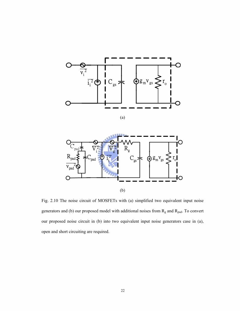
the excess noise generated by both pad and gate resistance. Fig. 2.10(a) shows the typical
noise circuit of MOSFETs with two equivalent input noise generators. However, this
simplified noise circuit did not consider the thermal noise from both gate resistance and
shunt pass resistance of probing pad. Fig. 2.10(b) shows the modified noise circuit
including the Rg and Rpad thermal noise sources. To include these additional thermal noises
12
and translate into the two equivalent input noise generators in Fig. 2.10(a), short and open
circuiting the input are required. The reason why open pad Rpad generates dominant noise
is due to the formation series or parallel connection with Rg during open or short circuiting.
Since the Rpad is larger than Rg even at the smallest 6 finger devices, its generated thermal
noise becomes the dominant factor in NFmin.
We have shown that the dominant noise source is from the probing pad
generated thermal noise, which is due to the lossy Si substrate effect. The NFmin is largely
reduced from the as-measured 3-6 dB to only small 1.1-1.2 dB after de-embedding for 6,
18 and 36 fingers 80 nm MOSFETs. The weak dependence of NFmin after de-embedding is
due to the combined effect of Rggm and nearly constant where the increasing finger number
decreases Rg but also increases gm monotonically.
13
Fig. 2.1 Two-port network
14
020406080
100120140
0 0.1 0.2 0.3 0.4 0.5 0.6
Lg (um)
Freq
uenc
y (G
Hz)
Fig. 2.2 The dependence of cut-off frequency ft on scaling down the Lg. ft is increased to
>100 GHz with 4 μm channel width and a finger number of 18 at 0.13 μm technology
node.
15
Fig. 2.3 The measured NFmin and associated gain at 10 GHz of n-MOSFETs using 0.13 μm
and 0.18 μm technology. The channel width is 4 μm and multi-fingered device layout is
used to reduce the gate resistance.
0.5
1.0
1.5
2.0
2.5
3.0
0 20 40 60 80
Finger number
NF m
in a
t 10
GH
z (d
B)
0
5
10
15
20
25
Ass
ocia
ted
gain
at 1
0 G
Hz
(dB
)0.13um MOSFETs
0.18um MOSFETs
16
Fig. 2.4 The dependence of ft on finger width under a fixed total gate width of 72 μm. The
ft increases to 130 GHz with 8 μm finger width and a finger number of 9 for 0.13 um
technology node.
110
115
120
125
130
135
140
0 2 4 6 8 10Wf (um)
Freq
uenc
y (G
Hz)
17
Fig. 2.5 The dependence of associated gain on finger width under a fixed total gate width
of 72 μm. The associated gain decreases monotonically with increasing finger width.
15
16
17
18
19
0 2 4 6 8 10Wf (um)
Ass
ocia
ted
gain
(dB
)
18
Lthru1
Csub 1
Rsub1
Rthru2 Lthru2PORT1 PORT2
Csub2
Rsub2RB
Rthru1
RgC
ox1Cox2
Rpad1
Cpad1
C'pad1
Rpad2
Cpad2
C'pad2
Fig. 2.6 The extrinsic equivalent circuit model for RF MOSFET that contains intrinsic
BSIM3 MOSFET model, connected gate resistance Rg, through transmission lines and
probing pads. The shunt impedance to ground from through line is much larger than
probing pad due to the short and thin line layout.
19
DUT
Fig. 2.7 The schematic diagram of probing pad and through transmission line connected to
device under test. Short and thin through line is used to reduce its noise generation.
20
0.5 1.0 2.0 5.0
-0.5j
0.5j
-1.0j
1.0j
-2.0j
2.0j
-5.0j
5.0jMag(S21)/3
S11
S12
S22
solid:simulationopen:measurement
(a)
0.5 1.0 2.0 5.0
-0.5j
0.5j
-1.0j
1.0j
-2.0j
2.0j
-5.0j
5.0jMag(S21)/8
S11
S22
S12
solid:simulationopen:measurement
(b)
Fig. 2.8 The as-measured and modeled S-parameters of 80 nm MOSFETs with probing
pad for (a) the smallest 6 and (b) the largest 36 gate fingers. The good agreement indicates
the good accuracy of model in Fig. 2.6. The S21 is divided by respective 3 or 8 to fit in the
unity radius Smith Chart due to the large gain.
21
0 2 4 6 8 10 120
2
4
6
8
as-measured NFmin equivalent circuit modeled NFmin
analytical calculated NFmin
modeled NFmin w/o pad
NFm
in (d
B)
Frequency (GHz)
(a)
0 2 4 6 8 10 120.0
0.5
1.0
1.5
2.0
2.5
3.0
3.5
4.0
as-measured NFmin
equiavlent circuit modeled NFmin
analytical calculated NFmin
modeled NFmin w/o pad
NFm
in (d
B)
Frequency (GHz)
(b)
Fig. 2.9 The measured and modeled NFmin of 80 nm MOSFETs with (a) the smallest 6 and
(b) the largest 36 fingers. The good agreement between as-measured and simulated NFmin
indicates the good accuracy of model in Fig. 2.6. The probing pad shows the dominant
effect on as-measured NFmin. The analytical calculation is also added for comparison.
22
Cgs
ro
gmvgsii2
vi2
(a)
Rg
Cgs
Rpad ro
gmv
gs
Vi2'
Cpad
Vg2
vpad2
ii2'
C'pad
(b)
Fig. 2.10 The noise circuit of MOSFETs with (a) simplified two equivalent input noise
generators and (b) our proposed model with additional noises from Rg and Rpad. To convert
our proposed noise circuit in (b) into two equivalent input noise generators case in (a),
open and short circuiting are required.
23
Chapter 3
Process Design and Considerations of
Metal-Insulator–Metal Capacitors
The improved high-frequency performance of CMOS devices after technology
scaling has led to more product designs with integrated mixed-signal/RF elements into
CMOS process. This chapter starts with the discussion of active/passive elements
necessary for mixed-signal/RF process and followed by the discussion of process concerns
while implementing MiM (metal-insulator-metal) capacitors into Cu-BEOL
(Back-end-of-Line) process.
3.1 Overview of Mixed-Signal/RF Components
Along with the technology scaling on CMOS, radio frequency (RF) performance
such as cut-off frequency (ft), maximum-oscillation frequency (fmax), and noise figure (NF)
have been improved. On the other way, the required performance metrics of digital and
analog devices are not common and require different strategies to optimize them. For
digital process, Idsat and Ioff are the key parameters for device design consideration. On the
other way, threshold voltage (Vt) and gm/gds are the prime consideration for analog design.
Traditional CMOS process development incorporated heavier channel dopant and halo
implant along with scaled technology. This process optimization will improve
short-channel effect but degrade gm/gds due to bias-induced barrier modulation at the drain
side. Therefore, process optimization will be required to integrate mixed-signal/RF devices
into CMOS digital process.
The key difference between digital and mixed-signal process is the existence of
24
passive elements. The passive elements for mixed-signal/RF design includes FEOL
(Front-end-of-Line) resistors, variable capacitors (varactors), vertical MiM capacitors,
lateral BEOL (Back-end-of-line) line-to-line capacitors, and inductors. These passive
components will limit the performance of mixed-signal/RF design. In mixed-signal/RF
design, these passive components are designed to perform active functions such as filtering,
tuning, gain control, and impedance matching. The performance of passive elements needs
to be specially considered while developing the process.
There are three kinds of FEOL resistors; un-silicided polysilicon resistors,
un-silicided diffusion resistors, and well resistors. Silicided resistors have much lower
sheet resistance (5~15 ohm/sq) and are not adequate for resistors in mixed-signal/RF
design. The design consideration on choosing FEOL resistors are sheet resistance, voltage
coefficient, and temperature coefficient. The voltage and temperature coefficients are
process-dependent (implant conditions, thermal cycle, and grain boundary size).
Un-silicided resistors require an extra silicide-block module. However, process
optimization for FEOL resistors are not specially considered in process development
because the main focus is to optimize active devices. Certain Boolean operation might be
applied on the resistor components to optimize the resistance targets. FEOL resistors will
require proper modeling to be implemented into mixed-signal/RF design.
Inductors are critical components in mixed-signal/RF design. Inductors with
small inductance and high-Q are employed in circuits such as RF transceivers. Larger
inductors with low-Q are utilized for impedance matching and gain control. Inductors are
usually implemented in the thicker upper layers of BEOL process to minimize resistance
and inductive losses to the dissipative silicon substrate. To form an inductor, a minimum
of two metal layers are required. One is to form the spiral and the other is to form the
underpass. The layout and material of the inductors will directly impact the maximum
25
achievable Q-factor of the inductors. Lower serial resistance by thicker metal layer will
improve the Q-factor at low frequencies and the inductive coupling to the substrate will
limit the Q-factor at high frequencies. Proper layout optimization and substrate leakage
path termination are key factors to improve the Q-factor of Inductors.
Precision/reference capacitors require tight matching and voltage/temperature
linearity and stability. There are four major types of capacitors used in
analog/mixed-signal design; polysilicon-insulator-polysilicon (PIP), metal-insulator-metal
(MiM), lateral line-to-line and metal over metal stack (MoM), and MOS capacitors. Best
performance is achieved by metal-insulator-metal (MiM) capacitors. MiM capacitors
possess excellent linearity with voltage/temperature and matching performance. MiM
capacitors are integrated near top of interconnect stack and require 1~2 additional mask
steps to form the capacitor structures. In recent years, the increasing interest of
analog/mixed-signal/RF processes has led to the implementation of MiM capacitors into
Cu-damascene process beyond 0.13 μm technology. There are some issues with MiM
capacitors while integrated with Cu-damascene process. The major concern is Cu
metallurgy and its impact on yield and reliability. The choice of insulator and bottom/top
electro-plates will affect the MiM performance. This chapter will discuss the process
integration of MiM capacitors with Cu-damascene process beyond 0.13 μm process
technology.
3.2 Process Concerns to Integrate MiM Capacitors into Cu
BEOL
High quality passive elements integrated with logic have been the trend of MS/RF
SoC. The on-chip integration of MiM capacitor and Inductors with logic process is
26
popular for area, cost, and performance enhancement. For 0.18 μm technology and
beyond, aluminum is used as the logic interconnects. While integrating MiM with Logic
process, one interconnect layer is usually used as the bottom electrode plate of MiM
capacitors. The thick Al interconnect (~4 k) offers a low-resistance and planar electrode
which results in a high-Q and low interface leakage. In the Cu back-end-of-line (BEOL)
era, the use of Cu as the bottom electrode plate is the most cost-effective method since
the Cu layer is also used for logic area without extra cost. Cu has also a very low
resistivity and results in a high-Q performance. Our results showed that Cu can achieve
Q~200 @2.4 GHz with 0.7 pF MiM capacitor. However, it had been reported that Cu
roughness will cause MiM reliability problem [17]-[19]. In addition, Cu can be used for
small area MiM but the performance will be significantly degraded for larger area MiM
capacitors. Cu metallurgical roughness and Cu-CMP u-scratch are two factors for the
worse early breakdown of MiM capacitors while Cu is used as bottom electrode plates.
To develop highly reliable, high-Q, and high-yield MiM capacitors, we have compared
different MiM bottom electrodes (Table 3.1), clarified the cause of reliability issue while
using Cu as bottom electro-plates, and developed an optimized TaN/Al/TaN bottom
electrode plate with highly reliable performance. The optimized method is to integrate
TaN/Al/TaN into Cu-damascene process as the bottom electro-plate but keep the
insulator dielectric and top electro-plate. The Q-value can achieve 115 @2.4 GHz with
0.7 pF MiM capacitor for TaN/Al/TaN bottom electro-plate. For pure TaN bottom
electro-plate, the Q-factor is significantly degraded more than half due to high resistivity.
For Al process, serious roughness was observed for thin Al layer. To resolve the
field-enhancement due to roughness of thin Al as bottom electro plate, we had developed
a method to optimize the process of aluminum deposition to fully resolve the roughness
effect. A high-Q, highly reliable, and capable of manufacturing MiM process in
27
Cu-BEOL is realized.
The key factor on designing MiM capacitor is the unit capacitance. Silicon dioxide
and silicon nitride are the usual insulator dielectrics of Metal-Insulator-Metal capacitors.
Silicon dioxide has been widely used as dielectrics of MiM capacitors due to easy
process integration with other materials and low leakage current. However, the dielectric
constant of silicon dioxide is ~3.9 that is not suitable for MiM capacitors with high unit
capacitance. As rule of thumb, MiM capacitors require silicon dioxide with thickness
~350 A as insulator dielectric to posses a unit-capacitance of 1 fF/μm2. Lower cost
processing requires much higher unit capacitance of MiM capacitors. The thickness of
silicon dioxide needs to be significantly reduced by half to achieve a unit-capacitance of
2 fF/μm2. The much higher leakage and reliability issues are the major concerns. To
successfully increase unit capacitance without causing process and reliability issues,
silicon nitride (Si3N4) are commonly used due to much higher dielectric constant (~7.5).
There is higher leakage current (>10X) of MiM capacitors while using Si3N4 as the
insulator dielectric. The higher leakage current needs to be taken into design
consideration while using Si3N4 as the insulator dielectric of MiM capacitor. There are
more researches studying on integration of high-k dielectrics (e.g. Ta2O5) into MiM
capacitors to increase the unit capacitance significantly.
3.3 MiM Capacitor Process
The process discussed in this chapter was based on a 0.13 μm CMOS
Mixed-Signal/RF process technology provided by IC foundry. There are two ways to
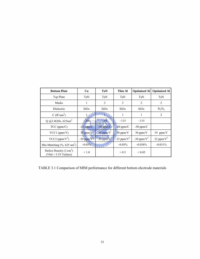
integrate Meal-Insulator-Metal capacitors into Cu-damascene process. One way is to use
Cu interconnect as the bottom electro-plate as shown in Figure 3.1. In this way, bottom
electro-plate is defined at the same time as other circuit interconnects after Cu CMP. The
28
insulator dielectric and top electro-plate are subsequently deposited and a mask layer is
required to define the top electro-plate. After top-electro-plate is defined,
inter-metal-dielectric (IMD) is deposited. Top via layer is subsequently defined to connect
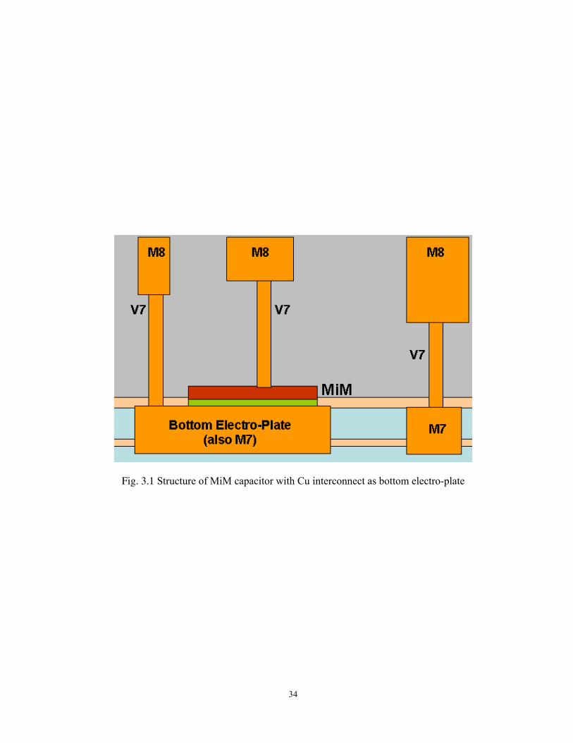
top electro-plate and bottom electro-plate at the same time. The other way of realizing
MiM capacitors is to insert MiM capacitors into the top two metal layers after processing
the FEOL and Cu dual damascene process. For an eight layers of Cu interconnect, MiM
capacitors are integrated into the BEOL process between seventh and eighth of Cu layer.
The reason of inserting MiM capacitor to the top two metal layers is because top metal has
larger process margin to cover the worse topography caused by MiM structure. By putting
MiM capacitor between top two metal layers, the parasitic capacitance to the silicon
substrate can also be reduced. The MiM structure is shown in Fig 3.2. After the 7th metal
layer was patterned after Cu-CMP, an etching-stop layer was deposited for further
processing. A thin TaN was deposited and sequentially followed by Aluminum and TaN
deposition to form the bottom plate with TaN/AlCu/TaN film stack.
Plasma-Enhanced-Chemical-Vapor-Deposition (PECVD) SiO2 or Si3N4 was then deposited
as the capacitor dielectric and followed by TaN deposition as top electro-plate. Two masks
were used to pattern the top electro-plate and bottom electro-plate. After oxide deposition,
via connection was formed to connect top-plate, bottom-plate, and Cu interconnect to the
eighth layer of metal at the same time. The etching recipe of Via process needs to be
optimized to properly land on bottom electro-plate and Cu interconnect but without etching
through the top electro-plate. The oxide topography due to the stacked MiM structure is
polished out by Cu-CMP while forming top metal interconnect. Therefore, the Cu
interconnect thickness above the MiM structure will be much thinner (~MiM structure
thickness) compared with the Cu interconnect without MiM capacitors beneath them. Due
to the much thicker bottom electroplate of TaN/AlCu/TaN structure, the gap filling is a
29
challenge for process integration. One way to resolve this issue is to properly define the
design rule and allow enough process marginality for gap filling between the MiM
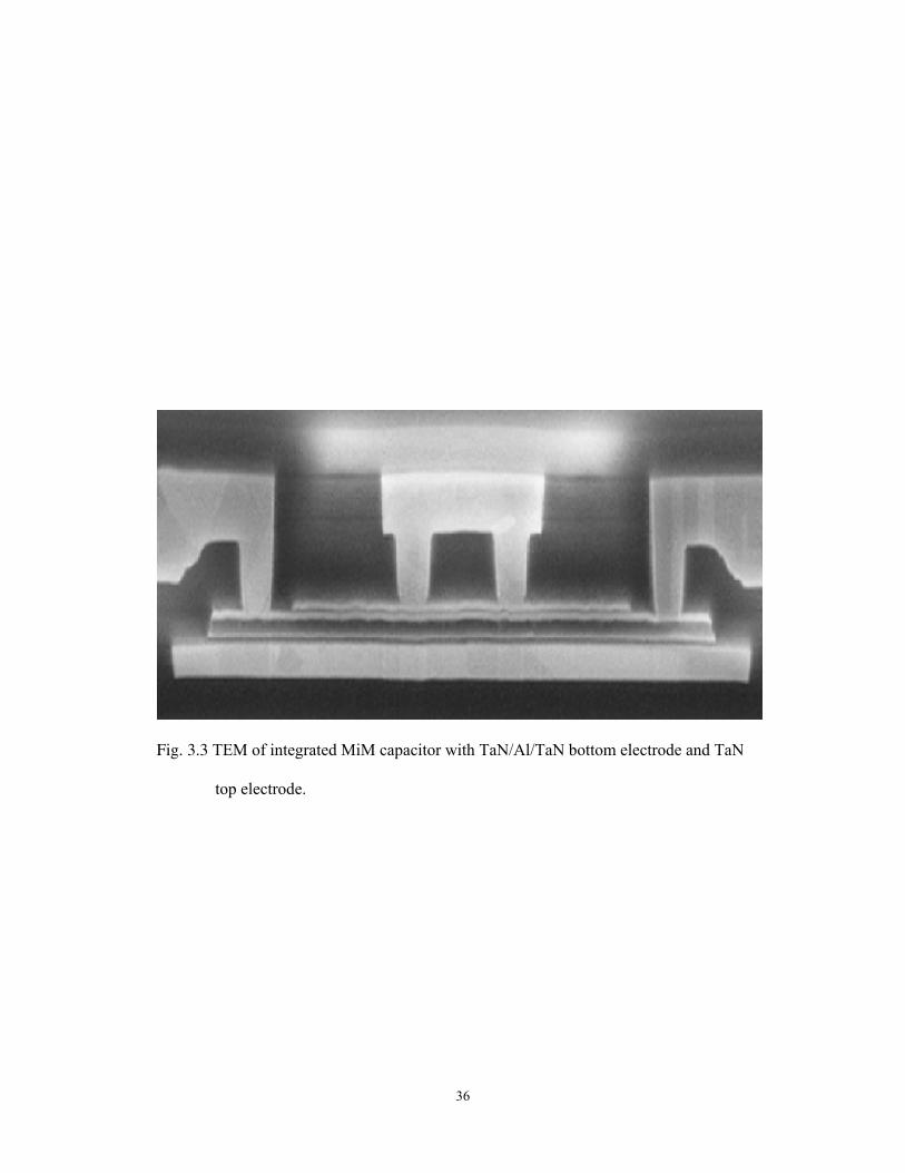
capacitors. Fig. 3.3 shows the TEM of integrated MiM capacitor with TaN/Al/TaN as
bottom electrode-plate and TaN as top electrode-plate.
3.4 Performance Characterization of MiM Capacitors
In this section, we characterize MiM performance of various materials as bottom
electrode-plate and insulator dielectrics. Q-factor, capacitance-voltage linearity,
voltage-temperature linearity, leakage current vs. voltage, and MiM breakdown voltage are
characterized and compared. The current-voltage (I-V), capacitance-voltage (C-V), and
quality factor (Q-factor) were measured by HP4156, HP4284, and HP8510C, respectively.
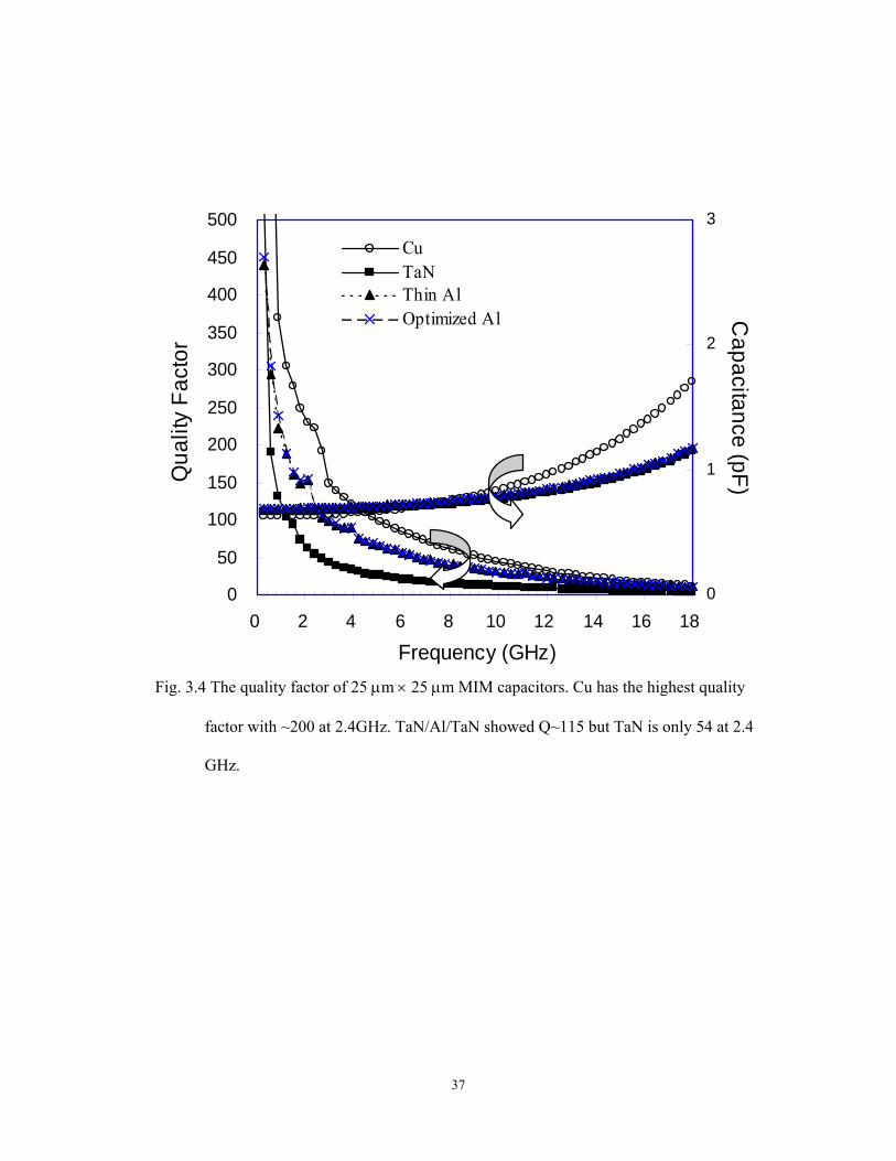
For RF application, the quality factor of MiM capacitors with different bottom
electrodes is shown on Figure 3.4. The quality factor can achieve ~200 for MiM capacitors
with Cu as the bottom electroplate and Q~115 for TaN/Al/TaN electrodes at 2.4 GHz
with 0.7 pF capacitance. For pure TaN bottom electroplate, Q factor can only achieve ~54
@2.4GHz due to higher resistivity. The capacitance increases at high frequency due to the
resonance of parasitic inductor, which can be flat out by proper de-embedding procedure.
From the Q-factor comparison among different materials as bottom electroplate, higher
Q-factor can be achieved by lowering down resistance of bottom electroplate. By using Cu
(also served as M7 for logic circuit) as bottom electroplate, the overall resistance reduction
is maximized due to lower resistivity and thicker Cu for interconnect. However, the factor
to influence the Q-factor of MiM capacitors is the series resistance along with this MiM
structure including resistance at both terminals of the MiM capacitors. Therefore, it is
favorable to put as many vias to connect top electroplate and bottom electroplate as
possible.
30
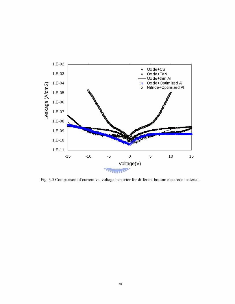
In additional to high-Q, another important factor of MiM capacitors is the leakage
current. This is especially important for high-density analog/RF ICs similar to the case in
DRAM capacitors [20], [21]. In this research, we reduced the MiM leakage current by
optimizing the MiM process. Typical leakage (J-V) behavior of different bottom electrode
materials is shown in Figure 3.5. The asymmetric leakage with applied voltage is due to
different surface roughness between top and bottom electrode-plates. For positive applied
voltage at the top electro-plate, electrons are injected from the bottom-plate to top-plate.
The roughness of the bottom electro-plate will be critical for creating sites with higher
electric field. Under low electric field, the trap-assisted tunneling (TAT) of electrons from
the electrode to trap states in the dielectric close to the electrode-dielectric interface will
dominate the capacitor leakage [22]. Nitride dielectric showed a higher MiM leakage
dependence with the applied voltage compared with Plasma-Enhanced Oxide (PEOX)
dielectrics. This is caused by the intrinsic leakage characteristics of silicon nitride film.
The leakage current is very low in the range of <1E-10 A/cm2 at 1.2 V for optimized Al
process condition with SiOx. On the other way, the impact of asymmetric leakage due to
different top and bottom electrode-plates is minor. The top electrode is deposited onto the
dielectric material and there is no surface roughness issue. The top electroplate is also
designed to connect the top metal line through via array and the resistance is much lower
compared with bottom electrode plate. Therefore, the impact to MiM performance is
minimal.
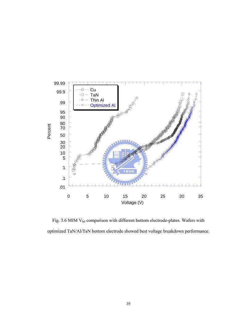
The comparison of MiM breakdown voltage (Vbd) performance is shown in Figure
3.6 with 1,000,000 um2 MiM area for bottom electrode-plates with TaN and Al and
640,000 um2 for bottom electrode-plate with Cu. The Vbd cumulative failure of Cu
electrode-plate is much worse than TaN and TaN/Al/TaN electrodes due to worse surface
roughness and inevitable Cu-CMP dishing. For small area MiM capacitors, Cu electrode is
31
still an option but high defect density will be a concern. For thin TaN/Al(<1.5 kA)/TaN
electrode, the surface roughness is observed to be critical which was not significant for
conventional Al(>3 kA)/TiN bottom electrode plate beyond 0.18 μm technology. By
optimizing the process temperature and other process conditions of Al deposition process,
the degradation of MiM Vbd by surface roughness is significantly reduced.
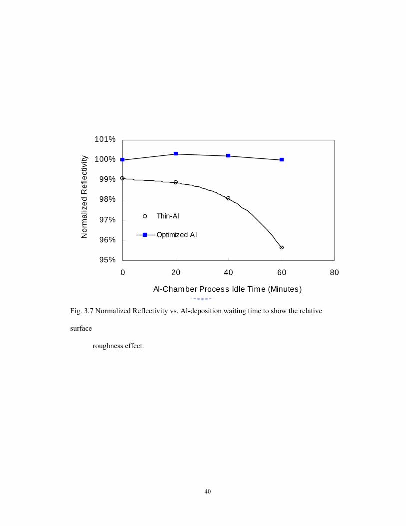
The reflectivity of TaN/Al/TaN electrode versus the waiting time of Al process also
demonstrated robust process after optimization as shown in Figure 3.7. Before the process
is optimized, the reflectivity will decrease significantly with process waiting time. For
optimized thin Al process, the dependence with the waiting time of Al deposition process
is negligible compared with original one. It indicates that the optimized Al deposition has a
stable surface roughness with manufacturable process window.
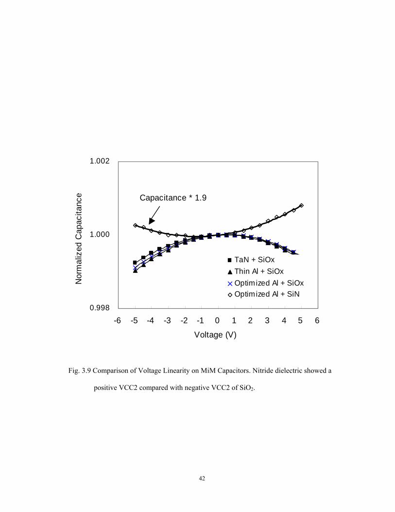
Linearity is a critical characteristic for capacitors. Figure 3.8 shows the normalized
capacitance of four different bottom electrode-plates versus temperature from 25 C to 125
C. Cu demonstrates minimal first-order temperature coefficient of capacitance with less
than 40 ppm/oC and ~30% reduction compared to that of TaN and TaN/Al/TaN. Figure 3.9
shows the normalized capacitance of three kinds of bottom electro-plates and two dielectric
materials versus the bias voltage from –5 V to 5 V. TaN demonstrated much better
first-order voltage coefficient of capacitance (VCC1) ~16 ppm/V compared with
TaN/Al/TaN ~30 ppm/V. The second-order voltage coefficient of capacitance (VCC2) is
comparable for different bottom electroplates. However, MiM dielectric with nitride has a
positive VCC2 (22 ppm/V2) compared to a negative VCC2 (-30 ppm/V2) for SiOx MiM
dielectrics. The negative second-order voltage coefficient of capacitance for SiOx
dielectrics is due to the intrinsic leakage current while applying voltage. The positive
VCC2 of silicon nitride film is due to charge trapping in the nitride film [23].
The development trend of MiM capacitor is to integrate high-k material to provide
32
a capacitor with high unit-area capacitance to minimize the chip area and reduce cost. The
study of interface reaction between high-k and electrode materials needs to be carefully
evaluated.
3.5 Summary
The incorporation of MiM capacitor into Cu-BEOL needs different approaches
from Al-BEOL process technology. The adoption of process options depends on the intent
of product design and MiM area. For high-Q and small MiM area product, Cu as a
capacitor bottom plate is a suitable option but has a lower process yield. We think Cu as an
bottom electro-plate is the best choice due to performance and simple process integration if
the poor Vbd performance can be resolved by process optimization. TaN-based MiM
capacitor can achieve low leakage and better linearity but a penalty of low quality factor
~54 @2.4 GHz due to higher resistivity. On the other way, a MiM capacitor with thin Al
bottom plate can be achieved with optimized process condition. The Al-base MiM
capacitor can achieve Q>100 at 2.4 GHz with ~0.7 pF capacitance. The optimized process
conditions can achieve a very low defect density and suitable for manufacturing. The
process design and performance comparison of integrating different MiM structures into
Cu damascene process is discussed in this chapter.
33
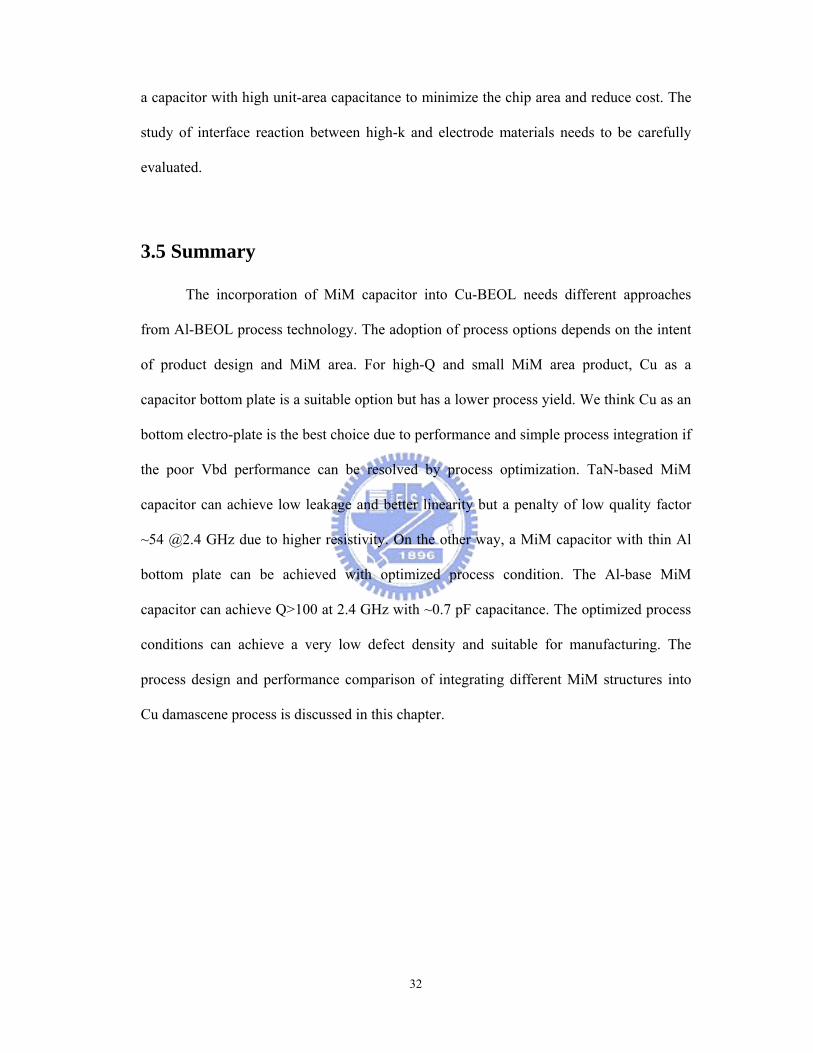
TABLE 3.1 Comparison of MIM performance for different bottom electrode materials
Bottom Plate Cu TaN Thin Al Optimized Al Optimized Al
Top Plate TaN TaN TaN TaN TaN
Masks 1 2 2 2 2
Dielectric SiOx SiOx SiOx SiOx Si3N4
C (fF/um2) 1 1 1 1 2
Q @2.4GHz, 625um2 ~200 ~54 ~115 ~115
TCC (ppm/C) -35 ppm/C -50 ppm/C -60 ppm/C -50 ppm/C
VCC1 (ppm/V) 30 ppm/V 16 ppm/V 30 ppm/V 30 ppm/V 55 ppm/V
VCC2 (ppm/V2) -30 ppm/V2 -30 ppm/V2 -33 ppm/V2 -30 ppm/V2 22 ppm/V2
Mis-Matching (%, 625 um2) ~0.05% ~0.05% ~0.038% ~0.031%
Defect Density (1/cm2)(Vbd < 3.3V Failure)
> 1.0 > 0.3 < 0.05
34
Fig. 3.1 Structure of MiM capacitor with Cu interconnect as bottom electro-plate
35
Fig. 3.2 Structure of MiM capacitor inserted between top two Cu layers
36
Fig. 3.3 TEM of integrated MiM capacitor with TaN/Al/TaN bottom electrode and TaN
top electrode.
37
Fig. 3.4 The quality factor of 25 μm × 25 μm MIM capacitors. Cu has the highest quality
factor with ~200 at 2.4GHz. TaN/Al/TaN showed Q~115 but TaN is only 54 at 2.4
GHz.
0
50
100
150
200
250
300
350
400
450
500
0 2 4 6 8 10 12 14 16 18
Frequency (GHz)
Qua
lity
Fact
or
0
1
2
3
Capacitance (pF)
CuTaNThin AlOptimized Al
38
Fig. 3.5 Comparison of current vs. voltage behavior for different bottom electrode material.
1.E-11
1.E-10
1.E-09
1.E-08
1.E-07
1.E-06
1.E-05
1.E-04
1.E-03
1.E-02
-15 -10 -5 0 5 10 15
Voltage(V)
Leak
age
(A/c
m2)
Oxide+CuOxide+TaNOxide+thin AlOxide+Optimized AlNitride+Optimized Al
39
Fig. 3.6 MIM Vbd comparison with different bottom electrode-plates. Wafers with
optimized TaN/Al/TaN bottom electrode showed best voltage breakdown performance.
0 5 10 15 20 25 30 35
.01
.1
1
51020305070809095
99
99.9
99.99CuTaNThin AlOptimized Al
Voltage (V)
Per
cent
40
Fig. 3.7 Normalized Reflectivity vs. Al-deposition waiting time to show the relative
surface
roughness effect.
95%
96%
97%
98%
99%
100%
101%
0 20 40 60 80
Al-Chamber Process Idle Time (Minutes)
Nor
mal
ized
Ref
lect
ivity
Thin-Al
Optimized Al
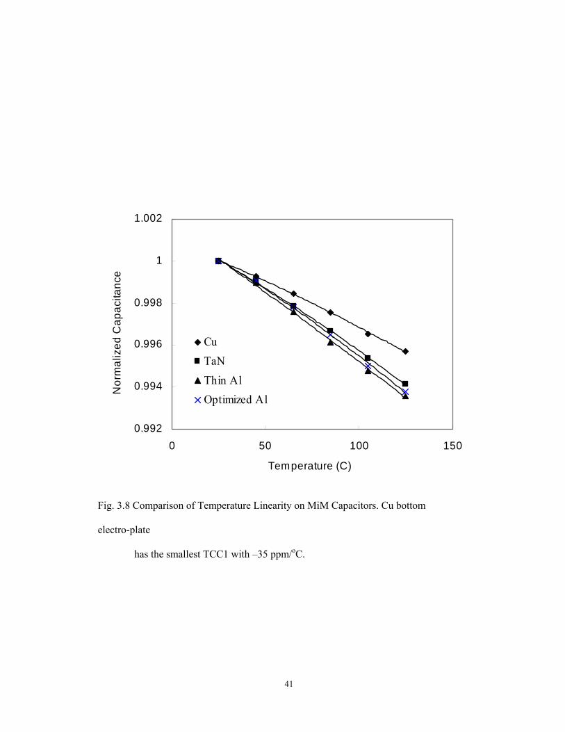
41
Fig. 3.8 Comparison of Temperature Linearity on MiM Capacitors. Cu bottom
electro-plate
has the smallest TCC1 with –35 ppm/oC.
0.992
0.994
0.996
0.998
1
1.002
0 50 100 150
Temperature (C)
Nor
mal
ized
Cap
acita
nce
CuTaNThin AlOptimized Al
42
Fig. 3.9 Comparison of Voltage Linearity on MiM Capacitors. Nitride dielectric showed a
positive VCC2 compared with negative VCC2 of SiO2.
0.998
1.000
1.002
-6 -5 -4 -3 -2 -1 0 1 2 3 4 5 6
Voltage (V)
Nor
mal
ized
Cap
acita
nce
TaN + SiOxThin Al + SiOxOptimized Al + SiOxOptimized Al + SiN
Capacitance * 1.9
43
Chapter 4
Asymmetric-LDD MOS Transistor for SoC Design
The improvement of RF performance along with technology scaling has made
CMOS the prime choice for RF-SoC design. However, the difficult part to realize a
transceiver on a single chip is to integrate power amplifier. The low drain breakdown
voltage of Si-MOS device is the most challenging issue to be resolved for RF-SoC design.
Therefore, we have proposed a new device structure based on current Si-MOS process
technology with 38% RF output power improvement at peak PAE by raised drain
operation voltage.
4.1 CMOS is the Trend for MS/RF SoC Design
The optimal technology choice for an RF application is complicated by many
factors; RF performance, wafer cost, level of integration, and time-to-market. GaAs
technology was expected to dominate the RF application because of its intrinsically higher
speed. Table 4.1 summarizes some key differences of the intrinsic material properties
between GaAs and Silicon [24]. GaAs has superior material properties for RF integrated
circuit over Silicon for the much higher low-field electron mobility and higher energy
efficiency due to direct band-gap. However, the evolution of CMOS technology has
improved the RF performance and offers a much lower process cost with high integration
with base-band circuit.
The technology scaling of CMOS process evolves with shorter gate length, thinner
gate oxide thickness, and lower operation voltage. Along with the improved device speed
and reduced cost per transistor, the maximum oscillation frequency (fmax) is also improved
larger than 50 GHz for 0.18 μm technology node [1]. At very short gate length (roughly
44
below 0.2 μm), the saturated drift velocity of the electrons dominates the cut-off frequency
(ft), and transistors fabricated in silicon and GaAs technologies have comparable cutoff
frequencies, albeit at higher voltage levels with the silicon-based devices [25]. These
technology improvements and cost reduction have made CMOS process the prime choice
for Mixed-Signal and Radio-Frequency (MS/RF) SoC. However, the realization of
high-power RF amplifier in 0.13 μm technology node is still a challenge due to the low
breakdown voltage of thin gate oxide thickness and device punch-through in conventional
MOSFETs. The limitation on breakdown voltage causes the low power gain in 0.13 μm
technology and beyond. This has made the design of RF power amplifiers in 0.13 μm
technology a difficult task.
Several device designs were introduced to improve the high-voltage breakdown of
MOS transistors such as LDMOS [12]-[14] and Drain-extended MOS [26]. However, these
devices are not suitable for RF SoC due to either low fmax or complicate process design.
The most challenging effort is to design high-voltage MOS transistors by using the
minimum gate length and core gate oxide thickness to gain the benefits of technology
scaling. On the other hand, the added process cost should be minimized or none. Therefore,
we have designed an asymmetric-LDD MOS transistor which can be further scaled. By
enlarging the gate length, the drain breakdown voltage will be further improved according
to the design requirements. The proposed asymmetric-LDD MOS transistor is suitable for
MS/RF SoC design.
Even though Silicon-based technology has become the dominant technology for RF
integrated circuit, GaAs (or InP)-based technologies will continue to maintain a small
portion of RF applications because of higher low-field mobility which has a direct impact
on device noise figure [27]. In some cases, even a few tenths of a decibel difference in
noise figure is significant for wireless applications; especially in base station and satellite
45
receiver.
4.2 Device Design of Asymmetric-LDD MOSFET
Low noise amplifies (LNA) are one of the key active components in an RF
system. Low noise and high linearity are required for LNA to content with a variety of
signals coming from the antenna. Two measures of these requirements are the amplifier
noise figure and the third-order input intercept point (IIP3); both determines the spur free
dynamic range (SFDR). The SFDR determines the difference between the maximum
detectable signal (MDS) and the maximum input signal prior to significant distortion [28].
In addition, high gain and low DC power consumption are other requirements of a LNA.
Power amplifiers (PA) for RF application must simultaneously satisfy
requirements of gain, linearity, output power, and power-added efficiency. Along with
technology evolution, the trend is to use lower power supply voltages. This makes it
difficult to maintain the required output power and efficiency due to impedance matching
limitations. Power amplifiers are typically operated in the Class-AB mode for most RFIC
applications to achieve a compromise between power-added efficiency and linearity. The
factors of key importance for amplifier performance are maximum oscillation frequency
(for high power gain), linearity (for lowest possible adjacent channel interference), and
breakdown voltage.
In conventional MOS transistor design, lightly-doped-drain (LDD) was
introduced to reduce the high electric-field at the drain side and improve the drain
breakdown voltage. However, this kind of MOS transistor design will provide a
conducting path from drain to the gate edge. Higher drain voltage will cause either gate
oxide breakdown or device punch-through under different gate voltages. To increase the
operation voltage at the drain side, a N+-P- junction at the drain side is designed for NMOS
46
transistor to reduce the maximum voltage beneath the gate electrode.
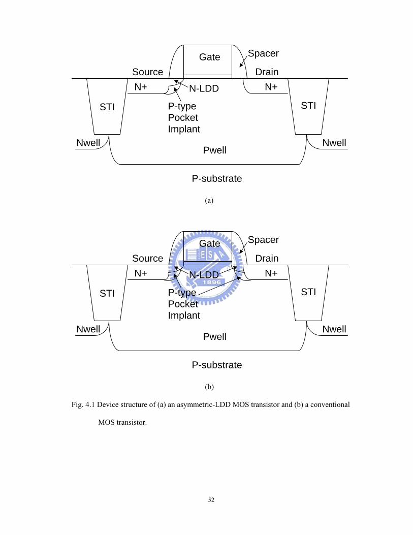
The structure comparison of (a) the new asymmetric-LDD MOS transistor and (b)
conventional MOS transistor are shown schematically in Fig. 4.1. Some different
asymmetric LDD structures [29]-[32] were used to increase current drive capability with
fully overlapped source implant. However, the fully overlapped source device has a worse
hot carrier injection and does not have a high voltage capability. To increase the transistor
breakdown voltage for RF power application, the LDD region at the drain side was
removed, which is the major difference to a conventional MOS transistor. This was
accomplished by blocking the ion implantations to LDD region and Halo process at the
drain side for the new transistor. The devices we studied in this work are multiple finger
MOS transistors with 10 gate fingers, 0.23 μm gate length and 5 μm width. For
comparison, the same interconnect and RF layout were used [7]-[11]. The schematics of
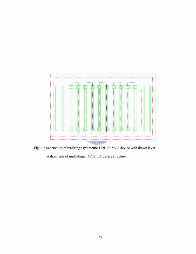
realizing asymmetric-LDD Si-MOS transistor is shown in Fig. 4.2. An extra layer was
drawn to be excluded during Boolean operation while generating LDD masks.
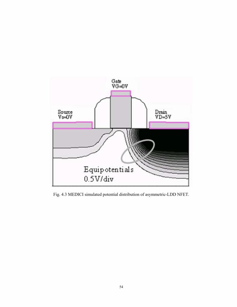
The applied drain voltage will create a depletion region formed by drain to channel
implant beneath spacer region. The depletion region will extend into the gate electrode
while applying higher drain voltage. At the same time, higher electric field in the depletion
region will have more voltage drop across the spacer region while applying higher drain
voltage. The MEDICI simulated potential distribution of asymmetric-LDD NFET is shown
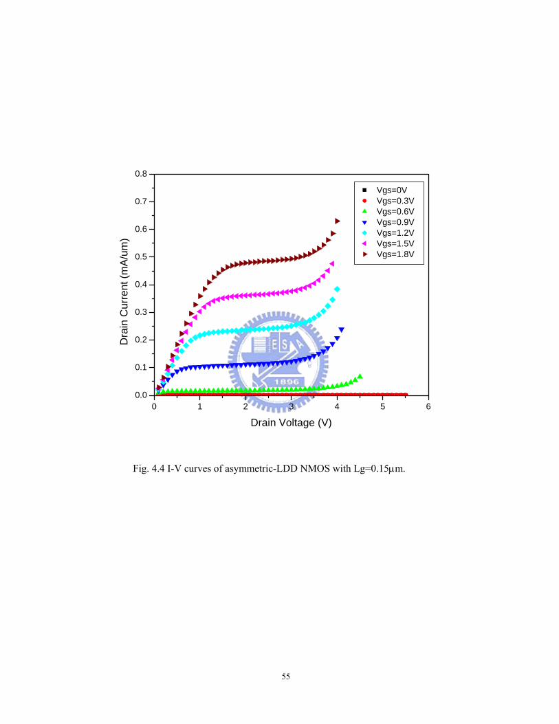
in Fig. 4.3. The Id-Vds curves with various gate voltages for an asymmetric-LDD MOS with
Lg=0.15 μm is also shown in Fig. 4.4.
The devices were fabricated by a standard logic process provided by IC foundry.
The RF power characterization was carried out by on-wafer measurements at 2.4 GHz
using an ATN load-pull system, where the input and output impedance matching
conditions were selected to optimize the output power.
47
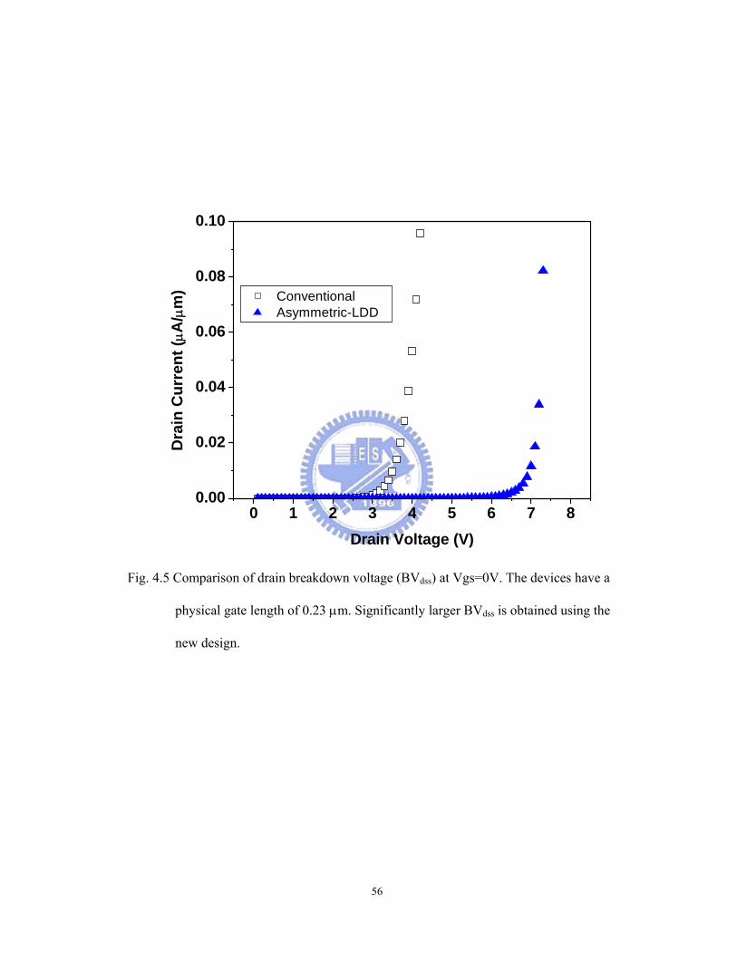
4.3 Drain Breakdown Voltage of Asymmetric-LDD MOSFET
Figure 4.5 shows the comparison of DC drain breakdown voltage for conventional
and asymmetric-LDD MOS transistors. For the conventional MOS transistor, a BVdss of 3.6
V was measured at Ids of 0.1 μA/μm and Vgs of 0 V. However, the maximum drain bias is
only 1.8 V if considering the reliability of 10 years continuous operation [7]. In sharp
contrast, the BVdss of the asymmetric-LDD transistor is increased to 7.0 V as measured
under the same criteria. This large improvement of BVdss is due to the designed wide
depletion region beneath the spacer region and between the drain and substrate. In contrast,
the existing n+-LDD in a conventional CMOS transistor just provides an electrically short
path between inversion channel and drain. Such wide depletion region in the new design
can support significantly larger reverse-biased drain voltage than conventional case. This
new device design with large drain depletion region is similar to bipolar transistor from the
device physics point-of-view. Since the electrons can pass through the drain depletion
region with fast saturation velocity under large reverse biased voltage, little degradation of
operation speed can be expected. Therefore, this new asymmetric-LDD MOS transistor can
effectively resolve the fundamental challenge of low breakdown voltage issue in the small
energy bandgap Si MOS transistor. In the meanwhile this device still preserves the high
frequency operation of sub-μm MOS transistors with cutoff frequency (ft) of 34 GHz close
to the 35 GHz of conventional MOS. This device also gives a higher maximum oscillation
frequency (fmax) of 86 GHz than the 76 GHz of conventional MOS. It is generally known
the increasing breakdown voltage may lower down the drive current. However, the new
asymmetric MOSFET can be operated at a higher voltage that gives close drive current
(10.44 mA at Vds=2.5 V) to conventional device (9.76 mA at Vds=1.8 V). One major
reliability issue for conventional deep sub-μm MOSFET is the Hot Carrier Injection (HCI)
48
degradation [33], caused by impact ionization and electrons injection into the gate oxide by
high drain field. Device structure with LDD and spacer was introduced to reduce the peak
electric field beneath the gate electrode that will cause serious hot carrier injection into gate
dielectrics. From detailed transistor simulation T-Supreme Medici Analysis (TMA) [34],
the asymmetric-LDD device design pushes the peak electric field away from the gate edge
and reduces the electron injection into the gate oxide. Thus, good HCI reliability may be
expected for this new device.
4.4 RF Power Performance of Asymmetric-LDD MOSFET
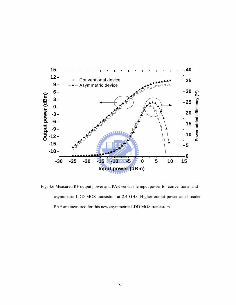
We have further measured the RF power performance in the asymmetric-LDD
MOS transistor. The output power and PAE versus the input power of both the
conventional and asymmetric-LDD MOS transistors are shown in Fig. 4.6. The DC bias
point of the conventional MOS transistor is at Vgs of 1.2 V and Vds of 1.8 V under the
maximum trans-conductance condition. For the asymmetric-LDD MOS transistor, the DC
bias point is at Vgs of 1.2 V and an increased Vds of 2.5 V. Here only 2.5 V is chosen in
this study although higher bias voltage can be used after detailed reliability study. The
output power is increased by 38% from 130 to 180 mW/mm, as measured at 2.4 GHz
under peak PAE condition. The PAE of asymmetric device at low input power is slightly
lower than conventional device, which may be due to inferior electron transportation
through the potential barrier at drain side. But this effect becomes less affective due to the
electron tunneling via potential barrier at high electric field and bias voltage. In addition,
broader maximum PAE region is also obtained in the asymmetric-LDD MOS transistor
that provides wider design margin, in combination with the slightly increasing peak PAE
from 23.5% to 24.9%. Moreover, when both devices are biased for 10 dBm output power
measured at 2.4 GHz, the PAE can be improved by 16%. These achieved large
49
improvements of power performance are a new breakthrough in RF Si CMOS transistors
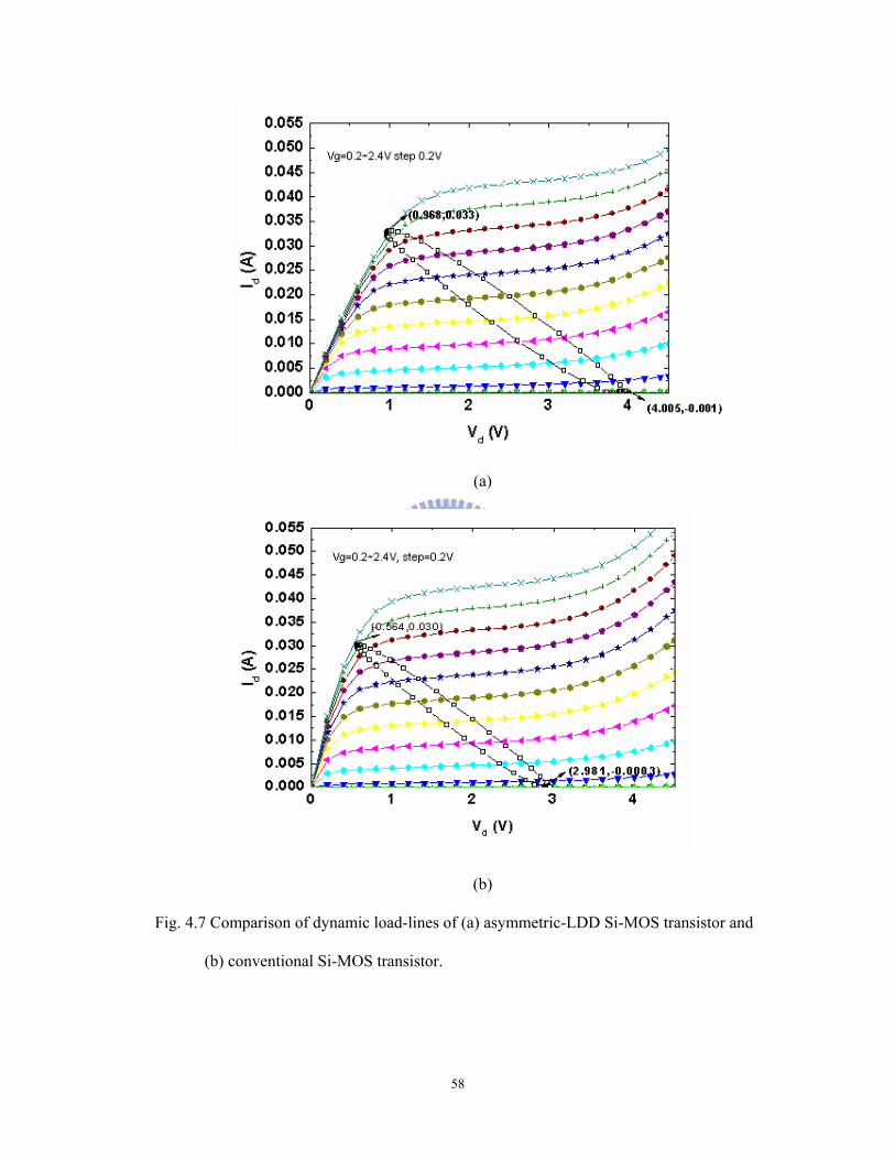
and important for wireless communication IC and SoC. The dynamic load-lines of both (a)
asymmetric-LDD Si-MOS transistor and (b) conventional Si-MOS transistor are shown in
Fig. 4.7 to illustrate the improved RF performance due to the choice of operation point
with raised drain voltage for asymmetric-LDD Si-MOS transistor.
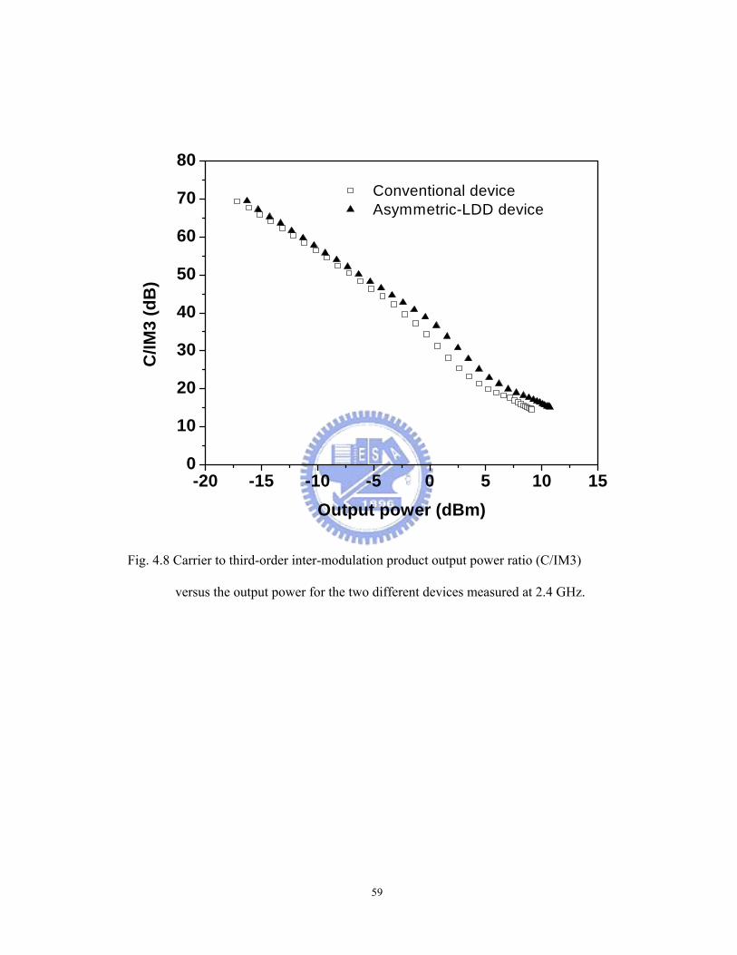
The carrier to third-order inter-modulation product output power (C/IM3) ratio is
another important factor for RF power application. We have compared the C/IM3 for the
two MOS transistors and the results are shown in Fig. 4.8. The asymmetric-LDD MOS
transistor still shows a slightly improved C/IM3 ratio of 0.7 dB at peak PAE. The
improvement is due to the reduced gate-drain coupling capacitance (Cgd) by removing the
LDD implant beneath the spacer; this reduces the interference between gate and drain
nodes and therefore improves the linearity. Therefore, significantly better output power
density is achieved by the asymmetric-LDD MOS transistor with even slightly better
linearity and PAE. However, the drain resistance (Rgd) is also increased along with
reduced Cgd, which causes an increased threshold voltage.
4.5 Summary
The low drain breakdown voltage of a conventional CMOS transistor is the
major restriction of RF power performance. We have designed an asymmetric-LDD MOS
transistor to increase the drain breakdown voltage from 3.6 V to 7.0 V. By raising the
drain operation voltage beyond conventional CMOS device, the RF output power of this
new transistor is improved by as much as 38% at peak PAE, with the added merit of
broader peak PAE region and useful for wider design margin. By removing LDD at the
drain side but keeping the spacer, an N+-P- depletion region is formed at the drain side.
The thickness of this capacitive depletion region is significantly larger than conventional
50
symmetrical design, which allows larger voltage applied to drain. Thus, this drain
engineering can improve the drain breakdown voltage and power performance. This new
asymmetric-LDD MOS transistor is fully embedded in the standard CMOS logic process
provided by foundries without any process modification.
Properties Silicon GaAs
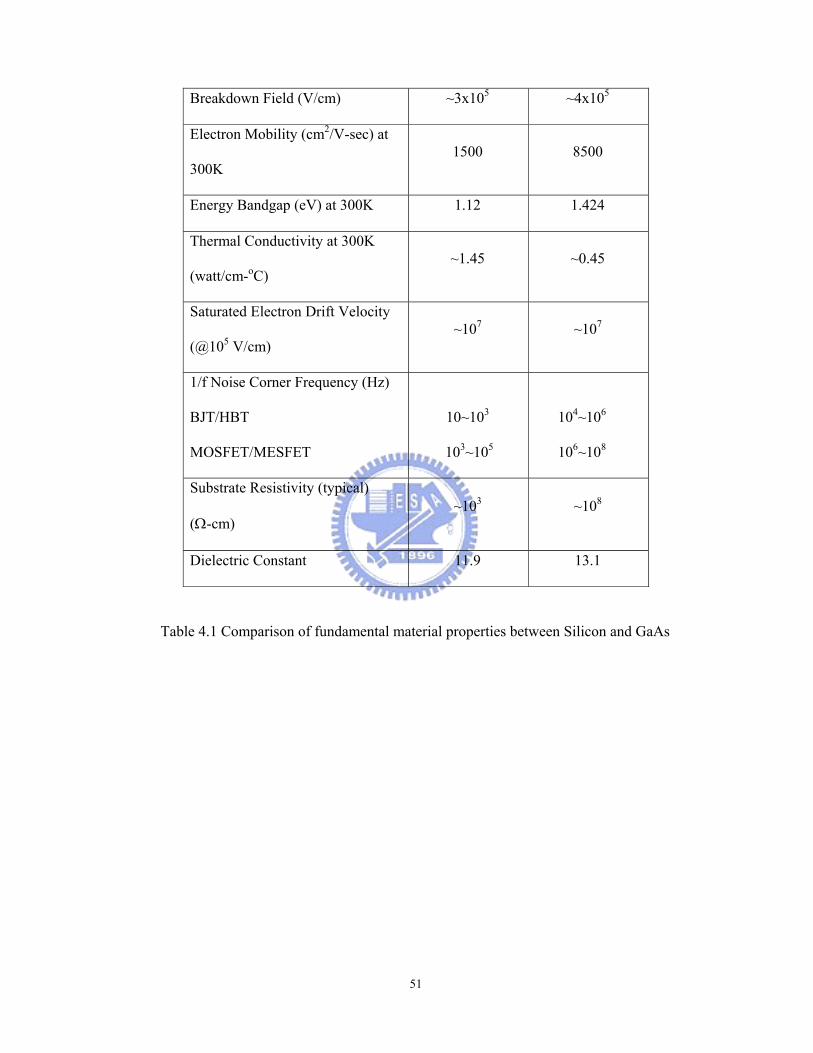
51
Breakdown Field (V/cm) ~3x10⁵ ~4x10⁵
Electron Mobility (cm2/V-sec) at
300K 1500 8500
Energy Bandgap (eV) at 300K 1.12 1.424
Thermal Conductivity at 300K
(watt/cm-oC) ~1.45 ~0.45
Saturated Electron Drift Velocity
(@105 V/cm) ~107 ~107
1/f Noise Corner Frequency (Hz)
BJT/HBT
MOSFET/MESFET
10~103
103~105
104~106
106~108
Substrate Resistivity (typical)
(Ω-cm) ~103 ~108
Dielectric Constant 11.9 13.1
Table 4.1 Comparison of fundamental material properties between Silicon and GaAs
52
(a)
(b)
Fig. 4.1 Device structure of (a) an asymmetric-LDD MOS transistor and (b) a conventional
MOS transistor.
STI STI
Gate
N+ N+
Spacer
N-LDD
PwellNwell Nwell
P-substrate
Drain Source
P-type Pocket Implant
STI STI
Gate
N+ N+
Spacer
N-LDD
PwellNwell Nwell
P-substrate
Drain Source
P-type Pocket Implant
53
Fig. 4.2 Schematics of realizing asymmetric-LDD Si-MOS device with drawn layer
at drain side of multi-finger MOSFET device structure.
54
Fig. 4.3 MEDICI simulated potential distribution of asymmetric-LDD NFET.
55
0 1 2 3 4 5 60.0
0.1
0.2
0.3
0.4
0.5
0.6
0.7
0.8
Dra
in C
urre
nt (m
A/um
)
Drain Voltage (V)
Vgs=0V Vgs=0.3V Vgs=0.6V Vgs=0.9V Vgs=1.2V Vgs=1.5V Vgs=1.8V
Fig. 4.4 I-V curves of asymmetric-LDD NMOS with Lg=0.15μm.
56
0 1 2 3 4 5 6 7 80.00
0.02
0.04
0.06
0.08
0.10
Dra
in C
urre
nt (μ
A/μ
m)
Drain Voltage (V)
Conventional Asymmetric-LDD
Fig. 4.5 Comparison of drain breakdown voltage (BVdss) at Vgs=0V. The devices have a
physical gate length of 0.23 μm. Significantly larger BVdss is obtained using the
new design.
57
-30 -25 -20 -15 -10 -5 0 5 10 15
-18-15-12
-9-6-30369
1215
Conventional device Asymmetric device
Input power (dBm)
Out
put p
ower
(dB
m)
0
5
10
15
20
25
30
35
40
Pow
er-a
dded
effi
cien
cy (%
)
Fig. 4.6 Measured RF output power and PAE versus the input power for conventional and
asymmetric-LDD MOS transistors at 2.4 GHz. Higher output power and broader
PAE are measured for this new asymmetric-LDD MOS transistors.
58
(a)
(b)
Fig. 4.7 Comparison of dynamic load-lines of (a) asymmetric-LDD Si-MOS transistor and
(b) conventional Si-MOS transistor.
59
-20 -15 -10 -5 0 5 10 150
10
20
30
40
50
60
70
80
C/IM
3 (d
B)
Output power (dBm)
Conventional device Asymmetric-LDD device
Fig. 4.8 Carrier to third-order inter-modulation product output power ratio (C/IM3)
versus the output power for the two different devices measured at 2.4 GHz.
60
Chapter 5
Conclusion and Future Works
5.1 Conclusions
Wireless communication has become more and more important among
various technologies that help people to communicate with each other and facilitate
our daily life. Wireless communication has been realized and evolved with better
quality, higher speed, and ease of usage. No matter the application is cellular wireless
communication through Global System for Mobile Communications (GSM), Code
Division Multiple Access (CDMA), or Wideband CDMA (WCDMA) or non-cellular
communication through Wireless Local-Area Network (WLAN), Bluetooth, Wireless
Personal Area Network (QPAN), or Ultra Wide-Band (UWB), wireless has shortened
the distance between people and ease our daily life. RF circuits realized by CMOS
technology are also playing a more important role in wireless communication as
CMOS technology keeps evolving. The much improved RF performance has made
RF-CMOS the prime choice for Mixed-Signal/RF SoC design.
In this dissertation, two key components for Mixed-Signal/RF design were
discussed; one is MiM capacitor and the other is RF-CMOS device. We have also
discussed how to optimize the RF performance by properly select finger number and
finger width and how to extract the intrinsic RF noise. The process design
consideration of implementing MiM capacitor into Cu BEOL process was discussed.
Different methods of implementing MiM capacitor into Cu BEOL were proposed and
the performance was compared. MiM capacitors with Cu as bottom electro-plat
achieved higher Q-factor compared with MiM capacitor with either TaN or
TaN/AlCu/TaN as bottom electro-plat due to much lower resistance. However, the
61
Vbd cumulative failure of Cu electrode-plate is much worse than TaN and
TaN/Al/TaN electrodes due to worse surface roughness and inevitable Cu-CMP
u-scratch. To balance the performance and reliability requirements, the proposed
MiM structure is to insert MiM capacitor between the top two Cu layers with
TaN/AlCu/TaN as the bottom electro-plate.
For high-Q and small MiM area product, Cu as a capacitor bottom plate is a
suitable option but has a lower process yield. TaN-based MiM capacitor achieved low
leakage and better linearity but a penalty of low quality factor ~54 @2.4GHz due to higher
resistivity. On the other way, a MiM capacitor with thin Al bottom plate had been achieved
with optimized process condition. The Al-base MiM capacitor achieved Q>100 at 2.4GHz
with ~0.7pF capacitance. The optimized process conditions also achieved a very low defect
density and suitable for manufacturing. The process design and performance comparison of
integrating different MiM structures into Cu damascene process was discussed.
A new asymmetric-LDD MOS device was proposed to improve the
drain-breakdown voltage but keeping the high-speed performance along with technology
evolution. The designed asymmetric-LDD MOS transistor demonstrated the increase of
drain breakdown voltage from 3.6 V to 7.0 V. By raising the drain operation voltage
beyond conventional CMOS device, the RF output power of this new transistor was
improved by as much as 38% at peak PAE, with the added merit of broader peak PAE
region and useful for wider design margin. This new asymmetric-LDD MOS transistor is
also fully embedded in the standard CMOS logic process provided by foundries without
any process modification
5.2 Future Works
62
The new asymmetric-LDD transistor has demonstrated better RF performance compared
with conventional CMOS devices. Our future work is to implement this new device into an
RF power amplifier and improve the power performance that is a critical part for
Mixed-Signal/RF SoC design.