Chapter 1 - DRUM - University of Maryland
128
ABSTRACT Title of Thesis: TEMPERATURE AND RATE DEPENDENT PARTITIONED CONSTITUTIVE RELATIONSHIPS FOR 95.5PB2SN2.5AG SOLDER ALLOY Shirish Anurag Gupta, Master of Science, 2003 Thesis Directed By: Dr. F. Patrick McCluskey Department of Mechanical Engineering One of the biggest challenges for power electronic devices is to be reliable in harsh environments. The operating temperatures in typical applications can go as high as 200ºC. The die attachment material of a power electronic device is one of the weak links in the system. The eutectic Sn-Pb solder alloy, which is the most commonly used permanent interconnect in electronics packaging cannot fulfill these service requirements, hence there is a need to find suitable replacements. Durability characterization is essential in order to accurately predict the reliability of the solder alloy chosen for the die attach material under life cycle loads. A large
Transcript of Chapter 1 - DRUM - University of Maryland

ABSTRACT Title of Thesis: TEMPERATURE AND RATE DEPENDENT
PARTITIONED CONSTITUTIVE RELATIONSHIPS FOR
95.5PB2SN2.5AG SOLDER ALLOY
Shirish Anurag Gupta, Master of Science, 2003 Thesis Directed By: Dr. F. Patrick McCluskey
Department of Mechanical Engineering
One of the biggest challenges for power electronic devices is to be reliable in harsh
environments. The operating temperatures in typical applications can go as high as
200ºC. The die attachment material of a power electronic device is one of the weak
links in the system. The eutectic Sn-Pb solder alloy, which is the most commonly
used permanent interconnect in electronics packaging cannot fulfill these service
requirements, hence there is a need to find suitable replacements.
Durability characterization is essential in order to accurately predict the reliability of
the solder alloy chosen for the die attach material under life cycle loads. A large

number of models are available, which can be used to determine the life of die attach
in small signal and power modules, however the shortfall of these models is the lack
of test data for all but the most common (e.g. eutectic Sn-Pb solder) die attach
materials. Hence, relevant constitutive properties must be measured, as they are
essential for quantitative characterization of damage accumulated in the die attach,
the knowledge of which is essential for accurate durability assessment.
The aim of this study is to determine the relevant constitutive properties for high
temperature high lead 95.5Pb2Sn2.5Ag solder alloy (Indalloy 163) by implementing
the direct local measurement technique. Temperature and loading rate dependent
mechanical and constitutive properties of the afore mentioned solder alloy have been
obtained by modeling the experimental data gathered by conducting monotonic,
isothermal, constant strain rate tests at a range of temperatures and strain rates
utilizing miniature single-lap shear specimens, with a partitioned form of the general
constitutive equation.

TEMPERATURE AND RATE DEPENDENT PARTITIONED CONSTITUTIVE
RELATIONSHIPS FOR 95.5PB2SN2.5AG SOLDER ALLOY
by
Shirish Anurag Gupta
Thesis submitted to the Faculty of the Graduate School of the University of Maryland, College Park in partial fulfillment
of the requirements for the degree of Master of Science
2003 Advisory Committee:
Associate Professor Patrick McCluskey Associate Professor Bongtae Han Associate Professor Peter Sandborn

©Copyright by
Shirish Anurag Gupta
2003

DEDICATION
To mom and papa, for their faith in me, and for always being my number one
supporters. The further I have traveled from them, the closer I feel to them. Without
their support, I couldn’t possibly have come this far.
ii

ACKNOWLEDGEMENTS
Thanks are in order for a bunch of people. To the 201 community over the years,
Deep, Harish, Nitin, Sumit, Vijay, Ankush, Neha, Shanon, Akanksha, and Vandana
for making a lot of hard times easier by just being there. To my colleagues Karumbu,
Arvind, Casey, Yunqi, Manas, Sudhir, Zeke, Christian, Luca, Will, Brian, and Witali;
just working with them has been a pleasure. To Anshul, Joe, Kaushik, and Dan, for
genuine support, friendship, advice, goodwill, and timely stress relief, especially
Anshul, for spending endless nights working in the ‘cave’…
To Dr. Kwon, for introducing me to the ‘art’ that is constitutive property
measurement, and to Yuri, for willingly sharing her experience of testing on the
Tytron. To Dr. Bongtae Han, for his guidance and understanding during the hard
times. To John, Dave, and Bob at the Physics Machine Shop for their excellent
workmanship and for expediting my work orders to help meet project deadlines.
Thanks to Siegfried Ramminger, Siemens AG, Munich for sponsoring the die attach
project, working on which has been enriching to say the least. To the faculty and staff
of the department of mechanical engineering and CALCE EPSC, who help keep the
program running like a well oiled machine, and to my thesis committee: Dr. Han, Dr.
Sandborn, and Dr. McCluskey, for sparing their valuable time to assess my work.
And most of all to my advisor, one of the nicest people I have met, for giving me
enormous flexibility, humor, guidance, patience, and understanding for the past two
and a half years.
iii

TABLE OF CONTENTS
List of Tables vi List of Figures vii Chapter 1. Introduction 1
1.1 Motivation 1 1.2 Die Attach Reliability Concerns 3 1.3 Literature Survey 6 1.4 High Temperature Pb-based Solders 8 1.5 Organization of Thesis 10
Chapter 2. Test Methodology: Direct Local Measurement Technique for Constant
Strain Rate Testing 12
2.1 Specimen Configuration 12 2.2 Specimen Preparation 14 2.3 Test Equipment – MTS TytronTM 250 MicroForce Testing System 16 2.4 Direct Local Measurement using Miniature Extensometer 20 2.5 Subtraction of Compliance Effects of Copper 23 2.6 Constitutive Modeling – A Partitioned Approach 27 2.7 Experimental Procedure – Determination of Constants 32
2.7.1 Time-independent Elasticity – Modulus Test 32 2.7.2 Time-independent Plasticity – Constant Strain Rate Test 33 2.7.3 Time-dependent Creep – Constant Strain Rate Test 35
Chapter 3. Implementation of Direct Local Measurement Technique for Constitutive
Property Measurements of 95.5Pb2Sn2.5Ag Solder Alloy 37
3.1 Modification of Solder Joint Geometry 37 3.2 Modification of Specimen Preparation Procedure for the
95.5Pb2Sn2.5Ag solder alloy 40 3.2.1 Preparation Procedure 41 3.2.2 Specimen Quality Verification 52
3.2.2.1 Non-destructive Testing 52 3.2.2.2 Destructive Testing 55
3.3 Experimental Set-up 57 3.4 Subtraction of Compliance Effects of Copper 59
iv
Chapter 4. Mechanical and Constitutive Properties of 95.5Pb2Sn2.5Ag Solder Alloy 64
4.1 Introduction 64 4.2 Yield Stress and Ultimate Tensile Strength 67 4.3 Time Independent Elasticity 71 4.4 Time Independent Plasticity 78 4.5 Time Dependent Steady-State Creep 84 4.6 Discussion 89
Conclusions 95 Contributions 97 Appendix A: Testing Procedures using MTS TytronTM 250 98 References 112
v

LIST OF TABLES Table 1.1: Die attach materials for high temperature applications 5 Table 1.2: Phase transition temperatures of a few Pb-based solder alloys 9 Table 3.1: Input properties of materials used in FEA 60 Table 4.1: Yield stress for 95.5Pb2Sn2.5Ag 68 Table 4.2: Ultimate tensile strength for 95.5Pb2Sn2.5Ag 70 Table 4.3: Elastic modulus as a function of temperature 75 Table 4.4: Elastic constants 77 Table 4.5: Young’s Modulii for lead-rich solders obtained from literature 78 Table 4.6: Time independent elastic constants 82 Table 4.7: Saturation stress and strain rate pairs for different temperatures 85 Table 4.8: Creep model parameters calculated from log-log plot 87 Table 4.9: Time dependent creep constants 89 Table 4.10: Comparison of creep model parameters obtained from literature 92 Table A.1: Tuning Values for 95.5Pb2Sn2.5Ag solder micro-shear lap specimen 101 Table A.2: Data Acquisition times for different strain rates 109
vi

vii
LIST OF FIGURES Figure 1.1: Simple small signal device plastic package design 4 Figure 1.2: One sided design of a power module 5 Figure 2.1: Iosipescu Uniform Shear Specimen Configuration 13 Figure 2.2: Specimen Configuration 14 Figure 2.3: The MTS TytronTM System 17 Figure 2.4: MTS Tytron™ Testing System Test Configuration 18 Figure 2.5: Extensions attached to specimen: Set-up 21 Figure 2.6: Extensions attached to specimen: Schematic 22 Figure 2.7: Extensions superimposed on specimen 23 Figure 2.8: Subtracting the effects of copper compliance on measurement of solder
deformation 25 Figure 2.9: Typical constant load creep test 30 Figure 3.1: Specimen Configuration with Modified geometry 37 Figure 3.2: 3-D Finite element Model of die attach 38 Figure 3.3: σx plotted as function of aspect ratio 39 Figure 3.4: σy plotted as function of aspect ratio 39 Figure 3.5: σz plotted as function of aspect ratio 39 Figure 3.6: τxy plotted as function of aspect ratio 39 Figure 3.7: Soldering Fixture 43 Figure 3.8: Schematic of Reflow Temperature Profile for 95.5Pb2Sn2.5Ag solder 46 Figure 3.9: Schematic of Reflow Temperature Profile for 95.5Pb2Sn2.5Ag solder 46 Figure 3.10: Typical solder joint as viewed under optical microscope 47 Figure 3.11: Typical solder joint as viewed under optical microscope 48 Figure 3.12: Early specimen: Severe Misalignment and Voiding 48 Figure 3.13: Void and poor width control 49 Figure 3.14: Poor width control 49 Figure 3.15: Voiding 49 Figure 3.16: Voiding 50 Figure 3.17: Voiding 50 Figure 3.18: Voiding 50 Figure 3.19: Voiding 51 Figure 3.20: Good solder joint quality 51 Figure 3.21: Good solder joint quality 51 Figure 3.22: Good solder joint quality 52 Figure 3.23: C-Scan of specimen A1-NiP-37 with SAM (no void) 54 Figure 3.24: C-Scan of specimen A1-NiP-24 with SAM (voids) 54 Figure 3.25: Cross-sectioned specimen A1-NiP-2 (early specimen) 56 Figure 3.26: Cross-sectioned specimen A1-NiP-34 56 Figure 3.27: Cross-sectioned specimen A1-NiP-37 56 Figure 3.28: Experimental Test Set-up for MTS Tytron™ Testing System 57 Figure 3.29: Close-up view of specimen mounted on machine 58 Figure 3.30 a): Finite Element Mesh generated for lap shear specimen 60

Figure 3.30 b): Deformed state (exaggerated) of specimen when an arbitrary force is applied at both ends 60
Figure 3.31: Mesh Convergence plot 61 Figure 3.32: Compensation Rate Curve obtained via FEA 62 Figure 3.33: Effect of compliance compensation on typical Stress strain curve 63 Figure 4.1: Test Matrix 64 Figure 4.2: Stress-strain curves at 25oC 65 Figure 4.3: Stress-strain curves at 80oC 66 Figure 4.4: Stress-strain curves at 125oC 66 Figure 4.5: Stress-strain curves at 150oC 67 Figure 4.6: Yield stress of 95.5Pb2Sn2.5Ag as a function of temperature 68 Figure 4.7: Yield stress of 95.5Pb2Sn2.5Ag as a function of strain rate 69 Figure 4.8: UTS of 95.5Pb2Sn2.5Ag as a function of temperature 70 Figure 4.9: UTS of 95.5Pb2Sn2.5Ag as a function of strain rate 71 Figure 4.10: Sample force vs. strain curve for specimen A1-10 at 25oC for Method 1
72 Figure 4.11: Temperature dependence of elastic modulus 76 Figure 4.12: Temperature dependence of Young’s modulii of some lead-rich solders
77 Figure 4.13: Sample force vs. strain curve at a constant strain rate of 1x10⁻⁴ and
temperature of 25oC 79 Figure 4.14: Equivalent stress vs. strain rate plot for different values of strain for
strain rates of 1x10⁻²s-1 through 1x10⁻⁶s-1 and temperature of 125oC 80 Figure 4.15: Strain rate-independent equivalent tensile stress vs. equivalent tensile
strain 81 Figure 4.16: Temperature dependence of strain hardening exponent 83 Figure 4.17: Temperature dependence of pre-exponential co-efficient 83 Figure 4.18: Log-log plot of equivalent steady state creep strain rate and equivalent
average saturated stress pairs 86 Figure 4.19: Temperature dependence of creep exponent 88 Figure 4.20: Arrhenius plot to determine creep thermal activation energy 88 Figure 4.21: Simplified creep deformation mechanism map 90 Figure 4.22: Schematic of log-log plot of shear creep rate vs. applied shear stress for steady state creep deformation of metals and alloys at high homologous temperatures 91 Figure 4.23: Comparison of model prediction and experimental data for steady-state
creep behavior 94 Figure A.1: Applied actuator axial strain rate 108
viii

Chapter 1. Introduction
1.1 Motivation
Electronic systems and components today are an integral part of practically every
type of product, be it for an industrial, business, consumer, or military application.
These electronic devices must perform the required electrical functions for which
they are designed in addition to maintaining their structural integrity while being
subjected to a wide range of environmental and operational loads. Common examples
of loads include vibration, shock, impact, bending, radiation, moisture ingress,
exposure to chemicals, and exposure to extremes of ambient and operating
temperature. All electronic devices are subjected to these loads with few exceptions.
Traditionally, commercial electronic devices have been designed to operate within a
small temperature range, with a maximum of 70oC, or 125oC for some automotive,
military, and avionic applications. However, performance and reliability of power
electronics systems and distributed control systems used for high temperature
applications such as oil well drilling and logging, nuclear reactor monitoring,
automotive engine control/monitoring, and aerospace applications, involving
operating temperatures in excess of 125oC (sometimes well over 200oC), need to be
examined. The high ambient temperatures of these applications when combined with
the inherent heat generation of power electronic systems can produce a very hostile
1

environment for electronics, which in turn leads to significant reliability concerns,
including low-cycle die attach fatigue [McCluskey et al., 1997].
Solder alloys, with high melting points are typically used in power electronic systems
as a large area die attach between the silicon die and the underlying substrate. At such
high operating temperatures, the common tin-lead eutectic solder cannot be used, as it
would melt before fulfilling service requirements (Tm=183oC). The use of high
temperature solders would reduce the load on cooling systems.
Durability characterization is essential in order to accurately predict the reliability of
the die attach material under life cycle loads. A large number of models are available,
which can be used to determine the life of die attach in small signal and power
modules, however the shortfall of these models is the lack of test data for all but the
most common (e.g. eutectic Sn-Pb solder) die attach materials. To this end, relevant
constitutive properties must be measured, as they are essential for quantitative
characterization of damage accumulated in the die attach, the knowledge of which is
needed for accurate durability assessment [Hong et al., 1995]. Solder alloys perform
at relatively high homologous temperatures (T>0.5Tm) in typical operating
conditions. Consequently, their mechanical behavior is highly nonlinear, and displays
a strong dependence on loading history and environmental conditions. Hence, the
behavior at different loading rates and temperatures must be analyzed. Nevertheless,
there is little or no information regarding the behavior of lead-rich solders, such as
95.5Pb2Sn2.5Ag alloy. It is important to not only analyze the response of the material
2

to temperature but also the response to loading rate, which gives valuable information
to reliability engineers in design of qualification tests. For example, temperature ramp
rates of thermal cycling tests can vary from 8oC/min to 20oC/min [Jedec standard,
1989]. The temperature ramp rate can also be 50oC/min in a thermal shock test,
which is used to assess the package integrity when subject to sudden temperature
change [Jedec standard, 1995].
This is the first study to concentrate on the temperature and loading rate-dependent
constitutive property measurements for 95.5Pb2Sn2.5Ag, a common, lead-rich, high
temperature solder, used as a die attach material in power electronic systems.
1.2 Die Attach Reliability Concerns
As mentioned, one of the biggest challenges for power electronic devices is to be
reliable in harsh environments. The operating temperatures in typical applications can
go as high as 200ºC. Not only do these devices have to operate at harsh ambients, but
also the environments are made harsher by the high power generation of devices,
which can sometimes be hundreds of watts per device. This power dissipation can
cause the temperature of the device to rise up rapidly when the device is switched on
and drop down rapidly when the device is switched off. These rapid temperature
changes upon repeated power on/off cycling can cause serious reliability concerns.
Due to the rapid power and temperature cycling of the device, the die attach which
connects the silicon (Si) chip to the substrate experiences high shear stresses due to
3

the cyclic differential expansion and contraction of the die and the substrate thereby
causing damage to accumulate in the die attach.
Figures 1.1 and 1.2 below demonstrate the fundamental differences between the
construction of a small signal device and a power module. The two main functions of
the die attach in small signal devices are to provide mechanical support to hold the
chip in place and to provide a low resistance thermal path for good heat dissipation of
the device. It is important that the device provide a low impedance thermal path so
that the chip temperatures are kept in range of reliable operation. In power devices, in
addition to these two basic functions of the die attach there exists a third, which is to
provide an electrical path to the drain on the bottom side of the device.
Fig. 1.1
Simple small signal device plastic package design
4

Fig. 1.2
One sided design of a power module
The ideal die attach should not only be electrically conducting, but it must also have a
co-efficient of thermal expansion, which matches well with that of the die and the
substrate to minimize the shear stresses it would be subject to during operation. In
addition, it should be compliant enough to absorb most of the stresses instead of
transferring them to the device or the substrate, which can cause additional reliability
concerns such as die and substrate cracking. Some of the potential die attach materials
for high temperature applications are listed in Table 1.1.
High modulus (stiff) Low modulus (flexible) Gold eutectics
Silver-filled glass
Silver-filled polyimides
Silver-filled epoxies
Lead-tin-based solders
Lead-rich solders
Indium-based solders
Table 1.1: Die attach materials for high temperature applications.
5

A compliant die attach, however, is more susceptible to failure due to fatigue. The
size of the die is also an important concern for reliability. Large area die attaches
develop higher stresses, also making them susceptible to failure by fracture. Thus for
a die size of less than 0.5cm, stiff materials like gold eutectics or silver filled glass,
polyimides, or epoxies are used for better fatigue resistance. For large area die
attaches in the range of 0.25cm2 to 6.25cm2, compliant attaches like lead-based or
indium-based solders are used to reduce stresses in the die.
1.3 Literature Survey
Early efforts to estimate reliability of electronics systems followed a strictly statistical
approach, where failure probability functions of individual components and
subsystems were combined in an appropriate manner to obtain a generic model to
predict the reliability of the whole system. The failure of individual components was
assumed to follow the traditional bathtub curve. However, no understanding of the
physical processes that cause these failures was included in this modeling approach.
Thus this method can only be applied to specific systems, and only after relevant
failure data are available. This method does not give an indication of the location or
source of the failure, or its root cause.
A more fundamental approach to constitutive property characterization of permanent
solder interconnections is similar to that used for traditional materials testing, viz. for
structural materials such as steel and its alloys.
6

The traditional test methods involve the use of bulk dog-bone shaped cylindrical
specimens, which are usually subjected only to axial displacements or loads in
tension or compression. Such methods are well developed and documented in ASTM
E8, E9, and E21. Various investigators have used these methods for their constitutive
characterization programs [Enke et al., 1989], [Frost et al., 1988], [Jones et al., 1997],
because of their relative ease of adaptability. Methods involving the use of such bulk
specimens neglects some fundamental aspects of application of these materials as
interconnects in electronics packaging. The dominant mode of deformation in solder
die attachments is shear due to differential thermal expansion of the die and the
substrate. Additionally, the volume of metal used in permanent interconnects are
small. Thus material response to load may be different for miniature interconnects as
compared to bulk specimens. Some researchers have performed tests to exclusively
compare the response of bulk specimens and miniature specimens. Raeder et al.
[1994] showed that single-lap shear joints of eutectic Sn-Ag solder are significantly
stronger than bulk specimens of the same material. Joint strengthening due to
dispersion of intermetallic layers in bulk solder, differences in grain size and resultant
creep deformation mechanisms, and geometry constraints in small joints or those with
high aspect ratios may also cause discrepancies in bulk solder and miniature specimen
behavior [Yang et al., 1996]. Thus it may be more appropriate to test solder
specimens that have length scales that are close to those of actual large area die
attaches. This has inspired investigators to use miniature specimens in their
experimental programs.
7

Other investigators have taken alternative approaches to constitutive property
measurement of solder alloys. A large number of programs utilize actual package
architectures [Darveaux, 1992], [Solomon, 1990], [Grivas et al., 1979], [Kashyap et
al., 1981], [Lam et al., 1979]. One approach uses ball indentation techniques to
measure constitutive properties such as hardness [Giannakopoulos et al., 1999;
Mahidhara et al., 1996].
In any successful approach, documentation of specimen preparation is critical.
Microstructure of as-cast and aged specimens can differ significantly thus altering its
mechanical response to loading, leading to variation in test data. As a result, the
specimen preparation procedure including the reflow profile and subsequent
processing steps must be kept standardized as far as possible throughout the course of
the testing program.
1.4 High Temperature Pb-based Solders
Before a solder alloy is chosen for service, it must satisfy a range of qualifications. In
addition to being cheap, it should be easily available and easily adaptable to existing
manufacturing processes. The solder should be compatible with other materials used
in the assembly. And finally, and most importantly, the solder fatigue properties must
be sufficient to satisfy the design requirements of the assembly. The choice of solder
alloy thus becomes an increasingly important issue, as it will depend on the service
8

requirement it is meant to fulfill. For example, 63Sn37Pb cannot fulfill service
requirements of 200oC operating temperature, since it has a melting point of 183oC.
Rather, materials with a melting point well above 200oC, such as lead-based, lead-
rich solders would be more suitable.
Phase transition temperatures of a few lead-based high temperature solders are
included in Table 1.2 [Hwang, 1996]. For practical applications three distinct
temperatures are used. Liquidus temperature is defined as the temperature, above
which the solder alloy is in stable liquid phase. Solidus temperature is defined as the
temperature, below which the solder alloy is in stable solid phase. Plastic Range is
defined as the temperature range between the solidus and liquidus temperatures of the
given composition, for which both the solid and liquid states co-exist in equilibrium
in the solder alloy. Eutectic temperature is defined as the temperature, at which a
single liquid phase is transformed into two solid phases.
Alloy Composition Solidus (oC)
Liquidus (oC)
Plastic Range (oC)
37Pb/63Sn (E*) 183 183 0
90Pb/10Sn 268 302 34
95Pb/5Sn 308 312 4
70Pb/30In 240 253 13
88.9Pb/11.1Sb (E) 252 252 0
97.5Pb/2.5Ag (E) 303 303 0
43Pb/43Sn/14Bi 144 163 19
20Pb/34Sn/46Bi (E) 100 100 0
92Pb/5Sn/3Sb 239 285 46
9

Alloy Composition Solidus (oC)
Liquidus (oC)
Plastic Range (oC)
18Pb/70Sn/12In (E) 162 162 0
92.5Pb/5In/2.5Ag (E) 300 300 0
36Pb/62Sn/2Ag (E) 179 179 0
92.5Pb/5Sn/2.5Ag 287 296 9
93.5Pb/5Sn/1.5Ag 296 301 5
95.5Pb/2Sn/2.5Ag 299 304 5
97.5Pb/1Sn/1.5Ag 309 309 0
Table 1.2: Phase transition temperatures of a few Pb-based solder alloys [*Note: (E) – eutectic alloy]
1.5 Organization of Thesis
Chapter 2 explains the Direct Local Measurement Technique (DLMT) developed by
Kwon et al. [2003] for the constitutive property measurements of lead-free solder
alloys used as permanent interconnections in Surface Mount Technology (SMT).
Chapter 3 describes the implementation of the DLMT for constitutive property
measurements of lead-rich 95.5Pb2Sn2.5Ag solder alloy used as a large area die
attach in power packaging.
Chapter 4 shows the experimental results of monotonic, isothermal, constant strain
rate testing of 95.5Pb2Sn2.5Ag solder. Temperature and loading rate-dependent
mechanical properties such as Yield stress and Ultimate tensile strength are obtained,
in addition to the temperature and loading rate-dependent elastic, plastic, and creep
properties. Creep model predictions are compared with experimental results.
10

Diffusion mechanisms for creep deformation are discussed and the diffusion
mechanism(s) responsible for creep deformation in 95.5Pb2Sn2.5Ag solder, for the
given test conditions, is identified.
Conclusions provide a summary of the thesis and the contributions. A list of relevant
books and articles is also provided for reference.
Appendix A contains detailed procedures for safe operation of the MTS TytronTM
250, in addition to relevant tuning and testing procedures.
11

Chapter 2. Test Methodology: Direct Local Measurement Technique for
Constant Strain Rate Testing
Solder alloys perform at relatively high homologous temperatures in typical operating
conditions. Consequently, their mechanical behavior is highly nonlinear, and displays
strong dependence on a loading history and environmental conditions. Thus,
temperature and loading rate-dependent constitutive properties of solder alloys are
important for accurate stress analysis, which are subsequently used to assess damage
accumulation due to life-cycle stresses.
The following sections of this chapter describe the Direct Local Measurement
Technique (DLMT) developed for constitutive property measurements of lead-free
solder alloys used as permanent interconnects in surface mount technologies [Lee et
al., Mar 2002; Lee et al., Oct 2002; Kwon et al., 2002; Kwon et al., 2003].
2.1 Specimen Configuration
As explained in Section 1.4, traditional testing methods involving the use of bulk
specimens neglect some fundamental aspects of material behavior when using solder
alloys as permanent interconnects in electronics packaging. The dominant mode of
failure in the actual permanent solder interconnect is shear, due to thermal expansion
mismatch between the die and the substrate. Also, the volume of the solder alloy in
these electronic assemblies can be extremely small. The properties of solder
12

interconnects are strongly dependent upon grain structure, which is governed by the
fabrication temperature and the joint size. It is desirable that the specimen be
fabricated under conditions as similar to the assembly reflow process as possible and
that its size is on the same order of the actual solder joints. For this reason, a
conventional simple tension test is not suitable for measuring the constitutive
properties of solder alloys. Miniature lap shear specimens better simulate the
geometrical and loading constraints of the permanent solder interconnects in actual
applications. Miniature specimens can have a single joint (single-lap shear), or two
joints (double-lap shear), or have multiple joints (arrayed-lap shear; flip-chip array).
Iosipescu [1967] has designed a specimen for single in-plane shear of metals or
composites utilizing a notched beam type sample, which is loaded so as to produce a
zero bending moment across the notch or test section. A typical Iosipescu specimen is
shown in Figure 2.1.
Fig. 2.1
Iosipescu Uniform Shear Specimen Configuration
Kwon et al. [2003] have improvised the modified Iosipescu micro-shear lap specimen
[Reinikainen et al., 2001] for uniaxial testing purposes. This specimen configuration
is shown in Figure 2.2; it retains the characteristic Iosipescu V-notch, which helps
minimize stress concentration at the edges and helps maintain a uniform shear stress
13

within the solder, while at the same time permits it to be mounted on a uniaxial test
frame. Kwon et al. [2003] have used a nominal joint height of 300µm to simulate the
geometric and loading constraints present in a solder bump. Nominal solder joint
dimensions are: 2.0mm x 1.5mm x 0.3mm.
Fig.2.2
Specimen Configuration
V-notch90°
2.2 Specimen Preparation
Good wetting of the solder to the copper requires the active surfaces be thoroughly
cleaned. Use of well-aligned and symmetric specimens with good axial linearity and
surface planarity reduces the stress developed simply through installing the specimen
into the test fixture on the machine. This simplifies the stress fields throughout the
solder thereby producing more uniform test data [Haswell, 2001]. Specimens are only
produced one at a time. Thus, it is imperative that the procedure be quick, repeatable,
and consistent. To this end, specimens are thoroughly cleaned with isopropyl alcohol
(IPA) and a special-purpose soldering fixture is designed for reflowing the solder
joint. Steel shims are wedged between the platens to maintain a joint height of
300µm. The key-shaped platens are made of cold-rolled copper and are obtained via
wire cutting (EDM).
14

15
Cleaning
The active surface of the platen (surface eventually in contact with the solder joint) is
made smooth using medium grade sandpaper. The platens are then dipped into flux,
and heated to activate the flux. The copper platen is brushed clean with IPA to
remove all debris on the surface. This step may be repeated as required.
Sealing
Silicone rubber is applied to the V-notch to prevent the flowing of solder down the
slope of the V-notch during reflow. The silicone rubber is left to cure for 12 hours.
Reflow Soldering
The platens are then located on the soldering fixture. The active surfaces are again
dipped in flux, which is activated as before. The fixture with the two key-shaped
platens is then placed on a hotplate, at 250°C, well above the melting point of the
alloy. The solder wire is brought in contact with the active surface, which is at a
temperature sufficient to melt the solder on contact and the solder fills the gap by
capillary action, creating the joint. The specimen is then gradually brought down to
room temperature using a thick aluminum cold plate as a heat sink. Specimens are
visually inspected for alignment and solder volume.
Polishing
Specimens are then polished mainly for two reasons: first, to reduce the specimen to
the desired thickness, and second, for axial linearity and surface planarity. Two
specimens are simultaneously mounted on a special-purpose polishing fixture to
increase planarity by increasing the bearing surface, and making it easier to maintain
orthogonality of the specimen during polishing. The specimen is polished on both

sides using multiple grades of waterproof metallurgical sandpaper (600, 800, and
1200 grit) from coarse grade to remove excess solder to fine grade for a highly
polished surface.
Inspection and Measurement of Joint dimensions
The specimen is inspected under an optical microscope for defects such as cracks or
surface voids and photographed for documentation purposes. Actual joint dimensions
are measured using digital micrometers and an optical microscope.
Pin press-fitting
If the specimen passes the visual inspection, holes in the copper platens are press
fitted with pins, which are used for mounting extensions (Please refer to section 2.4
for details).
Inspection
The specimen is again viewed under the microscope for any evidence of stress-related
damage to the joint due to press fitting.
Attaching extensions
The extensions are mounted using room temperature curing high temperature epoxy,
after which the epoxy is left to cure for 24 hours. The specimen is now ready for
testing.
2.3 Test Equipment – MTS TytronTM 250 MicroForce Testing System
Since typical solder interconnects in modern electronics are small, measuring the
mechanical behavior is a significant engineering challenge. The solder joint height is
16

very small (usually less than 500µm), and shear deformation is dominant. Most
specimens therefore require a very small gauge length. Displacement sensors or
gauges, which are easy to use with bulk specimens are often too cumbersome to be
used with these miniature specimens. Due to the small axial displacements recorded
in miniature specimens, the large gauge length and poor resolution of typical
displacement sensors induce errors in capturing meaningful test data. Such factors
contribute towards the choice of testing equipment to be selected for use. A micro-
mechanical tester is employed to document the solder deformations.
The MTS TytronTM is a uniaxial micro-tester for miniature specimens. It has a load
capacity of 250N and a load resolution of 0.001N. The system consists of the Tytron
250 load unit, the power amplifier, the Teststar IIs digital software, and the Teststar
system software. Figure 2.3 shows the system components.
Fig. 2.3
The MTS TytronTM System
17

18
The main hardware components of the load unit are the actuator, the reaction fixture,
the force transducer, and the measurement devices. A directly coupled linear DC
Servomotor drives the actuator, which is capable of speeds ranging from 1µm/hr to
0.5m/sec. It has a stroke of 100mm and is capable of frequencies of upto 50Hz. The
force transducer is mounted on the reaction fixture and is stationary. There are two
force transducers, with load capacities of ±10N (resolution: 0.0003N) and ±250N
(resolution: 0.0076N). There are three measurement devices besides the force
transducers, namely the linear variable differential transformer (LVDT), the
displacement gauge, and the miniature axial extensometer. The various components
of the load unit are depicted in Figure 2.4.
Fig.2.4
MTS Tytron™ Testing System Test Configuration
The LVDT is mounted on the actuator and measures displacement between the
actuator and the reaction fixture. It has a resolution of 1.83µm for the ±60mm
displacement range, and a resolution of 0.153µm for the ±5mm displacement range. It
must be kept in mind that when using the LVDT for measurement, the effect of the
ActuatorActuator
19
compliance of the entire load train must be accounted for and subtracted from the
measured displacement. The displacement gauge has a much higher resolution of
0.061µm for a ±2mm displacement range. The third device is the miniature
extensometer, which is by far the most accurate and useful since it makes direct strain
measurements possible, thus eliminating the compliance effects of the load train. The
extensometer (632.29F-20) has a 3mm gauge length and a resolution of 2.44µε
(0.0732µm) for the ±8% strain range and a resolution of 0.244µε (0.00732µm) for the
±0.8% strain range. In addition to these components, the TytronTM also has a
temperature controller and a temperature chamber. The temperature controller can
provide a temperature range of –75oC to 200oC and can control the temperature to
within ±1oC.
Detailed procedures for the safe operation of the MTS TytronTM 250 Tester are
explained in Appendix A, along with the relevant testing procedures used for
experimentation in this study.
Due to their small size, the axial stiffness, or compliance, of miniature specimens can
be very high compared to bulk specimens, thereby increasing the effect of the
compliance of the machine frame and load train on the experimental data. This
necessitates local measurement of solder deformation.
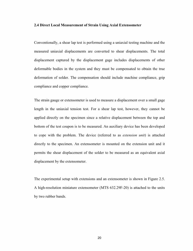
2.4 Direct Local Measurement of Strain Using Axial Extensometer
Conventionally, a shear lap test is performed using a uniaxial testing machine and the
measured uniaxial displacements are converted to shear displacements. The total
displacement captured by the displacement gage includes displacements of other
deformable bodies in the system and they must be compensated to obtain the true
deformation of solder. The compensation should include machine compliance, grip
compliance and copper compliance.
The strain gauge or extensometer is used to measure a displacement over a small gage
length in the uniaxial tension test. For a shear lap test, however, they cannot be
applied directly on the specimen since a relative displacement between the top and
bottom of the test coupon is to be measured. An auxiliary device has been developed
to cope with the problem. The device (referred to as extension unit) is attached
directly to the specimen. An extensometer is mounted on the extension unit and it
permits the shear displacement of the solder to be measured as an equivalent axial
displacement by the extensometer.
The experimental setup with extensions and an extensometer is shown in Figure 2.5.
A high-resolution miniature extensometer (MTS 632.29F-20) is attached to the units
by two rubber bands.
20

Fig. 2.5
Extensions attached to specimen: Set-up
Figure 2.6 illustrates how the unit is attached to the shear specimen. A pair of dowel
pins is inserted in the specimen by press fitting and the units are attached to the other
end of the pins using a room temperature curing high temperature epoxy adhesive.
With this configuration, the right-hand side unit has a relative horizontal motion with
respect to the left-hand side unit. When an extensometer is mounted in such a way
that each knife-edge is on each unit, the extensometer effectively measures the
relative displacement between the units, which can be related to the shear
displacement of the solder joint.
21

a)
b)
Fig. 2.6
Extensions attached to specimen: Schematic
The extensions are designed in such a way that the knife-edges of the extensometer
are exactly aligned with the pinholes of the extensions. The reason for this is simple;
the two extensions fixed atop the specimen do not come in contact with each other
and are free to translate along with the copper platen they are fixed to. In this way, the
extensometer is able to measure the deformation between the two pinholes on either
platen of the specimen, shown by points B and B' in Figure 2.7.
22

Fig. 2.7
Extensions superimposed on specimen
B & B' – at location of pins
A & A' – at Cu/solder interface
Specimen
Extension
Solder JointKnife-edge of extensometer
The extensometer measures the deformation between B and B'. But what is actually
required is the deformation between A and A', i.e. the actual deformation of the solder
joint. To put it simply, we need to find out the deformation between points A and B,
i.e. the deformation of the copper, and for that matter between A' and B' (same), and
subtract this apparent deformation from the measured deformation to obtain the actual
solder deformation.
2.5 Subtraction of Compliance Effects of Copper
This section explains the methodology proposed by Kwon et al. [2003] for
subtracting the effects of copper compliance on the deformation measurements made
using the extensometer to obtain actual solder deformation. Finite element analysis is
used to subtract the compliance effects of copper from the measured deformation. For
23

24
sake of convenience, the various terms used in this section are given the following
notations:
• Actual deformation of copper: ABδ
• Shear deformation of solder: 'AAδ
• Corrected deformation measured by extensions: 'BBδ
• Applied Force: appF
• Compensation Rate: )(CuCR
• Deformation measured by extensions: expδ
• Rotational correction factor applied to deformation measured by extensions: θδ
• Apparent deformation of copper: appδ
• Rotational correction factor applied to apparent deformation of copper: rotδ
The shear deformation of solder can be obtained by subtracting the compliance
effects of copper from the measured deformation,
ABBBAAδδδ 2'' −=
Let us define a point C on the periphery of the specimen and let us name the center
point of the solder joint to be S as shown in Figure 2.8. Rotational effects become
(2.1)

25
more and more pronounced as one moves from the point S towards the point B.
Therefore, the extensometer overestimates the deformation between points B and B'.
Fig. 2.8
Subtracting the effects of copper compliance on measurement of solder deformation
A rotational correction factor is applied to the measured deformation to obtain the
true measured deformation.
θδδδ 2exp' −=BB
Similarly, in an effort to estimate the actual deformation of copper, one must subtract
the rotational effects from the apparent deformation of copper. Therefore,
rotappAB δδδ −=
(2.2)
(2.3)

26
Aθ , Bθ , Cθ , and Sθ are the rotational angles of points A, B, C, and S, which are used
for calculation of the above rotational correction factors. Finite element analysis
(FEA) using the tool ANSYS® is employed to simulate the deformation of the
specimen under the application of an arbitrary force. Once all these above factors
have been calculated for a particular specimen thickness, the compensation rate can
be calculated by the formula:
app
AB
FCuCR δ2)( =
The finite element model may be solved for different values of thickness, and a plot
of compensation rate, defined as the compensation displacement per unit load, as a
function of the specimen thickness may be obtained.
This plot serves as a quick calculator of the compliance effects of the copper on the
deformation of the solder joint, for any specimen thickness, and can be immediately
subtracted to obtain shear deformation of solder. This is demonstrated by equations
(2.5) and (2.6).
ABAAδδδ 2exp' −=
where
)(CuCRFappAB ×=δ
(2.4)
(2.5)
(2.6)

27
It is important to note that the displacement to be compensated is only a function of
applied load and axial stiffness of the copper. The modulus of copper is obtained
experimentally using a copper strip specimen with a strain gage. The stress and strain
values are determined from the applied force and solder displacement respectively.
2.6 Constitutive Modeling
The stress-strain behavior for engineering materials is fairly complicated, and
depends on several factors, with temperature, strain (deformation) rate, and strain
history being the most important. An early concept in developing constitutive
equations was the idea that the flow stress was dependent only on the instantaneous
values of strain, strain rate, and temperature [Dieter, 1986].
0),,,( =Tf εεσ &
However it was soon realized that plastic deformation is an irreversible process. The
flow stress depends fundamentally on the dislocation structure, which depends on the
metallurgical history of strain, strain rate, and temperature. The general form of a
constitutive equation is given by,
dTT
dddTT εεεε
σεεσε
εσσ
&&
&&
∂∂
+
∂∂
+
∂∂
=
(2.7)
(2.8)

28
where ε is the uniaxial or equivalent strain, σ is the equivalent stress, T is
temperature, and ε& is the strain rate.
From a very basic perspective, deformation can be classified into two types, namely
recoverable elastic deformations and non-recoverable inelastic deformations.
Recoverable, in this case, means complete and instantaneous time-independent elastic
recovery although certain amount of anelastic i.e. time-dependent elastic recovery
does take place as well [Arrowood et al., 1991]. However, for all practical purposes
elasticity is described by a simple linear relationship between the applied stress and
measurable deformation, which is known as Hooke’s law:
)(TEelσε =
where E is the temperature dependent Young’s modulus of elasticity, σ is the
equivalent stress, and ε is the uniaxial or equivalent strain.
)()( 0 TEETE T−=
where T is the temperature. For most engineering materials and all solders, the elastic
modulus is temperature and strain rate dependent [Lau & Rice, 1992].
(2.9)
(2.10)

29
Modeling the inelastic behavior is far more complex, since it involves plastic and
creep deformation interactions. For the sake of convenience, plasticity is modeled as a
pseudo-instantaneous phenomenon, i.e. it is assumed to be time-independent, whereas
creep is time-dependent. Time-independent plasticity is typically modeled using a
power-law expression, commonly known as the Exponential Hardening model:
pnplK )(εσ =
where yσσ > and σy is the yield stress, K is the pre-exponential strength (hardening)
coefficient, and np is the plastic strain hardening exponent, which are modeled as
temperature dependent constants. Plastic deformations take place in conditions
wherein there is insufficient time for time-dependent deformation to occur, i.e. at
relatively higher strain rates. Since creep is a thermally activated process, plastic
deformation is prominent at low temperatures. Plastic behavior has a strong
dependence on temperature and strain rate.
However, since solders alloys are used at high homologous (T/Tm) temperatures, even
at room temperature, i.e. T>0.5Tm (Tm – melting point), more emphasis is placed on
creep deformation. A generalized scheme for modeling creep deformation is shown in
Figure 2.9. Accumulation of creep deformation can be divided into three steps. The
strain rate starts high (primary creep), but decelerates into a lower, steady state value.
This is the region where the creep strain rate is saturated and is known as steady state
creep strain rate (secondary creep). Eventually, the strain rate begins to increase
(2.11)

30
rapidly eventually leading to failure by creep rupture (tertiary creep). The secondary
creep strain region is the one that is most often modeled, and chosen to represent the
entire creep process; the reason being that modeling steady state creep eliminates the
need for inclusion of strain history.
Fig.2.9
Typical constant load creep test
Weertman’s steady state power law is used for modeling the steady state, secondary
creep strain rate [Tribula & Morris, 1990; Pao et al., 1993]:
RTQ
nvcr eA c
−
=1
σε&
where A is the stress co-efficient, 1/nc is the creep strain hardening exponent, Q is the
thermal activation energy of creep, R is the Bolztmann constant, T is the absolute
temperature, crε& is the equivalent creep strain rate, and σv is the equivalent saturation
creep stress.
(2.12)

31
Various other steady-state creep models employed in the literature include the
hyperbolic sine [Wang et al., 1998; Darveaux et al., 1993; Frear et al., 1996], the
Norton model [Mukai et al., 1998; Hall, 1987], variations of the partitioned creep
model [Wong et al., 1988; Shine et al., 1988], variations of the Sherby-Dorn model
[Kashyap et al., 1981; Langdon et al., 1977]. Other investigators chose to model the
primary creep behavior [Darveaux et al., 1997], which can be significant in certain
conditions. In some cases, plasticity can be represented in a unified manner, using a
single expression to represent both the time-independent and the time-dependent
deformation. Examples of this type of modeling scheme are the Bodner-Partom
unified creep-plasticity model [Skipor et al., 1996], and the Anand model [Anand,
1982; Wilde et al., 2000].
Thus, by adding the separately calculated elastic, plastic, and creep deformation, the
partitioned constitutive relationship gives us the total strain and is given by,
)()( tt crpleltot εεεε ++=
where totε is the total deformation of the solder joint, elε is the time-independent
elastic deformation, plε is the time-independent plastic deformation, and crε is the
time-dependent creep deformation, which can also be expressed as,
(2.13)

32
( ) RTQ
nTn
tot etATKTE
t c
p −+
+=
1)(1
)()()( σσσε
where is ε the equivalent strain and σ is the equivalent stress.
2.7 Experimental Procedures – Determination of Constants
The values of the material constants in the constitutive model developed above are
obtained experimentally. A test matrix is developed to determine the time
independent behavior (elastic and plastic) and time dependent creep behavior. The
tests are conducted for a range of constant strain-rates and temperatures. The
procedure for determining the elastic, plastic and creep properties is explained below.
2.7.1 Time-independent Elasticity - Modulus Test
Isothermal monotonic tests are conducted in strain control mode to obtain the linear
load-displacement curve. After the first measurement, the specimen is flipped and
measured again. The two values are averaged to negate the effect of misalignment.
The elastic modulus of solder alloys is a function of strain rate as well as temperature
[Shi et al., 1999]. However, the strain rate effect on modulus is not investigated here.
A shear strain rate ( 13101 −−×= sγ& ) is used for modulus tests because it is reasonably
close to the actual strain rate of solder in microelectronic packages under normal
operating conditions. Modulus tests are performed for a temperature range designed
to simulate field-loading conditions. For the tests at the elevated temperatures, an
(2.14)

33
environmental chamber is placed at the test section to maintain the test temperature,
and the grips with longer rods are installed to connect the specimen to the testing
machine. The long arm makes an initial alignment more difficult. A copper strip with
strain gages on both sides is used to help the initial alignment. Due to the extremely
small strain to be measured for the modulus test, specimen-to-specimen variations are
often observed. Tests are conducted on several specimens to check for consistency of
data. The raw data is averaged to minimize possible random errors.
After subtracting the compensation displacement, the true load-displacement curve is
obtained. It is then converted to the shear stress-shear strain curve using the
geometrical parameters of the solder joint, from which the shear modulus can be
determined. Subsequently Young’s modulus can be calculated by using the
relationship of the elastic constants, assuming a suitable value for the Poisson ratio, ν,
using engineering judgment.
2.7.2 Time-independent Plasticity - Constant strain rate test
Implementing the constant strain rate test has advantages over the creep (constant
load) test. With the constant strain rate test, rate-dependent properties as well rate-
independent properties can be determined, which can reduce the total number of tests
significantly. Another practical advantage is that undesired data can be screened out
at the early stage of the tests. If the specimen has defects and thus a crack grows
during the test, a significant load drop is visible in the load-displacement curve. Also,

34
since a low strain rate test usually runs for 40~60 hours, it is extremely time-effective
if the specimen with defects is detected at the early stage of test.
The tests are conducted for a range of constant strain rates at the pre-determined
temperatures. For the constant strain rate tests, the bending effect associated with
misalignment of the specimen is not significant because sufficient plastic flow occurs
during the test to eliminate the effect [ASTM Std E1012-99].
Separating the plastic flow into an effectively strain rate-independent stress-strain
curve and strain rate-dependent plastic flow processes is difficult. One way to get an
approximately strain rate-independent curve is to extrapolate the flow stresses vs.
strain rate curve at each value of strain to very high strain rates where the increase in
the flow stress is minimal for the corresponding strain rate. Defining the extrapolated
value of flow stress at a very high strain rate to be the true unrelaxed stress for a given
value of strain, and finding such a value for different values of strain allows one to
obtain a stress-strain curve that is approximately strain-rate independent [Mavoori et
al., 1997].
Shear stress can then be converted into an equivalent tensile stress and shear strain to
an equivalent tensile strain by applying the Von Mises yield criterion to obtain the
relationships [Meyers et al., 1984],
γετσ3
1,3 == (2.15)

35
From the data obtained through the above method, the time-independent exponential
hardening constant and the pre-exponential co-efficient can be calculated by curve
fitting.
2.7.3 Time-dependent Creep – Constant Strain Rate Test
In general, time-dependent creep behavior can be characterized by a data set
consisting of a steady-state strain rate and a saturation stress. The data are usually
obtained from creep (constant load) tests. In creep tests, the strain rate is constant in
the secondary (steady-state) creep regime, at a constant applied load. In this research,
however, constant strain rate tests were conducted to obtain the data set. In a constant
strain rate test, the load increases at a constant strain rate, and eventually the flow
stress reaches its steady state saturated value, and is constant.
The tests are conducted at a range of temperatures and strain rates. After converting
the shear components into the equivalent tensile components, saturation stress and
strain rate pairs obtained from the constant strain rate tests at different temperatures
were plotted on a log-log scale. The creep exponent, the stress co-efficient, and the
thermal activation energy for creep can be calculated as follows,
vc
cr nRTQA σε ln1lnln +−=&
(2.16)

36
The constant term, RTQA−ln , can be decomposed into the co-efficient and the
activation energy by plotting vs. the inverse of temperature. The y-intercept gives the
co-efficient and the slope gives the activation energy.
This methodology has been implemented successfully for constitutive property
measurement of lead free solder alloys used as permanent interconnects in surface
mount technologies. However, modifications are required before this methodology
can be adapted for the determination of the constitutive properties of high
temperature, high lead solder die attaches such as the 95.5Pb2Sn2.5Ag alloy. These
issues are addressed in Chapter 3.

Chapter 3. Implementation of Direct Local Measurement Technique for
Constitutive Property Measurements of 95.5Pb2Sn2.5Ag Solder Alloy
The following sections of this chapter describe the implementation of the Direct
Local Measurement Technique for constitutive property measurement of
95.5Pb2Sn2.5Ag solder alloy, used as a large area die attach in power packaging.
3.1 Modification of Specimen Geometry
In this study, a nominal joint height of 100µm was used to simulate the geometric and
loading constraints present in a large area die attach. Nominal test specimen solder
joint dimensions were: 2.0mm x 1.5mm x 0.1mm. Figure 3.1 shows the specimen
configuration used.
Fig. 3.1
Specimen Configuration with Modified Geometry
V-notch90°
0.1mm
2.0mm
1.5mm
Finite element analysis was employed to verify if the above specimen configuration is
an accurate simulator of actual die attach constraints. A three-dimensional (3-D) finite
37

38
element model was developed using ANSYS® as shown in Figure 3.2. The model of
the die attach was subject to normal (tensile) and shear loading.
Fig. 3.2
3-D Finite element Model of die attach shown for t/w=1
{t – thickness (depth), w – width, h – height}
The model was solved for different t/w aspect ratios (keeping the width constant) to
ascertain whether the specimen with a t/w of 0.75 could accurately represent the die
attach. The above figure is shown for an aspect ratio of 1 (t/w=1). To assess the effect
of die attach thickness (depth), stresses at center point in mid-plane were plotted for
different values of thickness. When t/w = 2.5, all stresses started to saturate and there
was no apparent stress difference for t/w greater than 2.5. Maximum stress difference
for σx was less than 2.2%. Maximum stress difference for σy was less than 0.9%.
However, maximum stress difference for σz was more than 130% and appeared to be
largely affected by thickness. Such a large percent difference is misleading because σz
was found to be negligibly smaller in magnitude as compared to other stress
w
t h
x
z
y

39
components. Maximum stress difference for τxy was less than 0.06% and also
negligible. As observed from Figures 3.3, 3.4, 3.5, and 3.6, between two cases of
t/w=1 and t/w=0.75, the stress differences were 0.7%, 0.3%, 51% and 0% for σx, σy,
σz, and τxy, respectively. The dotted circles denote stress differences for aspect ratios
0.75 and 1.
Fig. 3.3
σx plotted as function of aspect ratio
Fig. 3.4
σy plotted as function of aspect ratio
Fig. 3.5
σz plotted as function of aspect ratio
Fig. 3.6
τxy plotted as function of aspect ratio
As mentioned earlier, the effects of σz were neglected despite the large percent stress
difference for the two aspect ratios. The stress differences for the remaining three
stresses were also negligible, and one could safely conclude that because shear stress

was the dominant mode of deformation, a specimen with an aspect ratio of 0.75
(t/w=0.75) could simulate the constraints in the actual die attach (t/w=1) with
minimal effect of change in thickness. If the thickness of solder specimen was
increased from t/w=0.75 to t/w=1, it could better simulate actual die attach
constraints, however, the specimen preparation and testing method would become
more complicated. Hence t/w=0.75 was maintained throughout the program.
Increasing or decreasing the height of the solder joint may affect the stress/strain
fields and subsequently the mechanical properties of the material, e.g. the relative
grain size and the intermetallic layer will have a pronounced effect when joint height
is reduced to the scale comparable to the grain size of solder. It should be noted that
this analysis did not consider the solder joint height since the height used (100µm)
was on the same scale as that of a die attach used in actual assemblies.
However, before the specimen with the new joint height of 100µm could be used for
testing, several alterations were required to be made to the specimen preparation
procedure explained in Section 2.2. These changes are described in detail in Section
3.2 below.
3.2 Modification of Specimen Preparation Procedure for the 95.5Pb2Sn2.5Ag
solder alloy
The material properties of the solder joint depend on its microstructure. A stable and
40

consistent microstructure significantly improves the repeatability of experimental
data. The microstructure of the joint depends on its size and the reflow temperature
profile. An optimum reflow temperature profile can be developed with the accurate
knowledge of the phase transition temperatures of the solder alloy. The solder
material in this study is the high temperature, high lead 95.5Pb2Sn2.5Ag solder with
a joint height of 100µm. Thus, suitable modifications must be made to obtain
specimens with a stable and consistent microstructure.
3.2.1 Preparation Procedure
The copper platens were initially manufactured at the Physics Machine Shop at the
University of Maryland, College Park. However, later it was decided to prepare the
platens at Infineon Technologies AG using Wieland® K80 copper, first electroplated
with nickel (depth - 1µm), then chemically (electroless) plated with Ni-P (depth -
3µm). This simulated the process followed by Infineon Technologies AG for
soldering the chip to the substrate in high power devices. It is known that at the
Cu/solder interface, Sn reacts rapidly with Cu to form a Cu-Sn intermetallic
compound (IMC), which weakens the solder joint due to the brittle nature of the IMC.
The strength of the solder joint decreases with the increasing thickness of the IMC
formed at the interface and the IMC acts as initiation sites for micro-cracks [Alom et
al., 2002]. The electroless Ni-P plating improves the interface properties. Studies
have shown that that a Ni/solder interface has a much slower IMC growth rate as
compared to a Cu/solder interface. Ni thus acts a diffusion barrier between Cu and the
solder in order to sustain a longer period of service [Chan, et. al., 1998]. The effect of
41

the interactions at the Cu/solder interface is not accounted for in this study and is
beyond the scope of this thesis.
The basic requirements in producing quality specimens are cleanliness of active
(eventually soldered) surfaces and precise alignment of the two platens used. To this
end, the active surfaces were first cleared of contaminants by smoothing with a
medium fine grade (1000-A) sand paper and then rinsed thoroughly with IPA to
remove any remaining debris.
A special-purpose soldering fixture was designed for reflowing the solder joint.
Dowel pins were used for locating the platens on the fixture such that the two active
surfaces are precisely aligned. Figure 3.7 shows the modified soldering fixture used
for reflow soldering. Since the gauge diameter of the wire used as raw material is
800µm, small pieces of the wire had to be cut, twisted into a braid and flattened as far
as possible to fit it in the 100µm gap between the two copper platens. Steel shims
were wedged between the platens to maintain a joint height of 100µm. The platens
were held tightly in place by a screw driven plate, which also helps maintain the two
platens parallel to each other during reflow.
42

Fig. 3.7
Soldering Fixture
Steel shim Aluminum insert Dowell pin
Wire braid Solder joint
fixture Specimen
It was essential to control the actual solder joint dimensions as close to the nominal
dimensions as possible to avoid variations in experimental data due to erroneous
estimation of stress and strain. Silicone rubber could be used for preventing the flow
of solder down the slope of the V-notch during reflow soldering at temperatures
above 260oC, since Dow Corning® heat resistant sealant No.736 has a maximum
usable temperature of approximately 260oC for intermittent exposure. It was decided
that an insert acting as a plug, fitting the V-notched square gap at either side of the
eventual solder joint, be used for the purpose rather than the silicone rubber.
A cheap, easily available and easily fabricated material, namely, aluminum was
chosen as the material for the insert. Aluminum has a high melting point (660oC) and
is not wetted by solder. The silicone rubber has a curing time of 12 hours. Thus, using
aluminum inserts not only helped control solder joint width, but also helped to
significantly reduce the specimen preparation time, since curing time was saved.
43

44
The reflow profile used had five main parameters:
• Preheating time
• Preheating temperature
• Peak temperature
• Dwell time at peak temperature
• Cooling rate
And consisted of the three heating stages:
• Preheating
• Flux activation hold
• Spike and reflow
The preheating temperature needed to be set to permit sufficient time to activate the
flux. The flux used in this study was a rosin-based mildly activated flux (Kester #186
type RMA – 61% 2-Propanol, 39% Rosin), which was specified for activation
between 130oC and 150oC. The wrong preheating profile could cause insufficient
fluxing or decomposition of the organic flux. The third stage was to spike the
temperature quickly to the peak reflow temperature (usually 1-2oC/s) to avoid
charring or overdrying of the organic flux. Peak temperatures used are generally 25-
50oC higher than the liquidus temperature of a particular solder alloy, for example,
the typical peak temperature for SnPb eutectic solder is 233oC for a liquidus
temperature of 183oC.

Another important parameter is dwell time at peak temperature. The wetting ability is
directly related to the dwell time at peak temperature. Peak temperature and dwell
time were set to obtain an optimum balance between good wetting, minimal void
formation and low intermetallic compound formation. The dwell time was short
enough to minimize intermetallic formation, while being long enough to achieve good
wetting and to expunge any non-solder (organic) ingredients from the molten solder
before it solidified, to minimize void formation [Hwang, 1996].
The liquidus temperature of the 95.5Pb2Sn2.5Ag solder is 304oC. Reflow soldering
was conducted at a peak temperature of 380oC in an effort to simulate the peak
temperature encountered by assemblies during reflow at Infineon Technologies AG.
Figure 3.8 shows the schematic of the reflow temperature profile for the
95.5Pb2Sn2.5Ag solder alloy, and Figure 3.9 shows the actual reflow profile used. As
can be seen, flux activation was carried out at 130oC and reflow at 380oC. The
specimen was cooled down to room temperature by setting it on a thick aluminum
cold plate used as a heat sink. Optimum parameters for reflow were established using
the above guidelines, as well as engineering judgment and experience. Figure 3.10
shows the typical solder joint under the optical microscope.
45

25
75
125
175
225
275
325
375
425
0 20 40 60 80 100 120 140
Time (sec)
Tem
pera
ture
(o C
)
Liquidus Temperature
Dwell time at Peak Temperature
Cooling
Spike & Reflow
Peak Temperature
Flux Activation Hold
Preheating
Fig. 3.8
Schematic of Reflow Temperature Profile for 95.5Pb2Sn2.5Ag solder
25
75
125
0 20 40 60 80 100 120 140
Time (sec)
175
225
275
325
375
425
Tem
pera
ture
(o C)
Fig. 3.9
Actual Reflow Temperature Profile for 95.5Pb2Sn2.5Ag solder
46

47
Fig. 3.10
Typical solder joint as viewed under optical microscope
There were a few key issues during specimen preparation, which if ignored could
have resulted in poor specimen quality:
• Improper location on fixture- caused specimen misalignment leading to stress-
related damage during subsequent steps.
• Improper cleaning and flux activation- caused poor joint quality, e.g. voiding
or poor wetting of solder to copper.
• Flowing of solder along the Iosipescu grooves- caused joint dimensions to
deviate from the nominal dimensions leading to erroneous stress-strain
calculations.
• Incorrect reflow temperature profile- caused variations in joint microstructure
and hence variation in measurements.
• Stressed joint during polishing and pin press fitting- caused interfacial cracks
and delamination of the joint, which shifted the failure mechanism from the
bulk of the solder joint to the Cu/solder interface. This was usually manifested
as a sudden load drop in the load-displacement curve.

48
Figures 3.11 to 3.22 give an idea of the specimen preparation process concerns.
Errors were separated into four major categories:
• Misalignment of copper platens
• Poor width control
• Poor Wetting
• Voiding
Each error source was isolated and corrected one at a time.
Fig. 3.11
Early specimen: Misalignment, voiding, poor width control
Fig. 3.12
Early specimen: Severe Misalignment and Voiding
(Designed new reflow fixture)

Fig. 3.13
Void and poor width control
(Designed Aluminum inserts for width control)
Fig.3.14
Poor width control
(Designed new reflow fixture)
Fig.3.15
Voiding
(Varied flux amount, preheat time, and dwell time at peak temperature)
49

Fig. 3.16
Voiding
(Varied flux amount, preheat time, and dwell time at peak temperature)
Fig. 3.17
Voiding
(Varied flux amount, preheat time, and dwell time at peak temperature)
Fig. 3.18
Voiding
(Varied flux amount, preheat time, and dwell time at peak temperature)
50
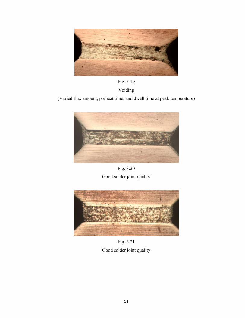
Fig. 3.19
Voiding
(Varied flux amount, preheat time, and dwell time at peak temperature)
Fig. 3.20
Good solder joint quality
Fig. 3.21
Good solder joint quality
51
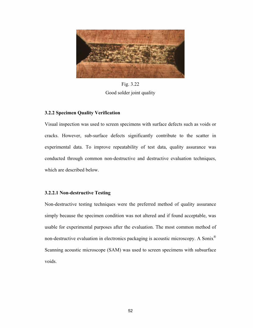
Fig. 3.22
Good solder joint quality
3.2.2 Specimen Quality Verification
Visual inspection was used to screen specimens with surface defects such as voids or
cracks. However, sub-surface defects significantly contribute to the scatter in
experimental data. To improve repeatability of test data, quality assurance was
conducted through common non-destructive and destructive evaluation techniques,
which are described below.
3.2.2.1 Non-destructive Testing
Non-destructive testing techniques were the preferred method of quality assurance
simply because the specimen condition was not altered and if found acceptable, was
usable for experimental purposes after the evaluation. The most common method of
non-destructive evaluation in electronics packaging is acoustic microscopy. A Sonix®
Scanning acoustic microscope (SAM) was used to screen specimens with subsurface
voids.
52

In acoustic microscopy, a piezoelectric transducer emits and scans ultrasonic pulses
of energy across the surface of a part, which is immersed in a water bath. The
ultrasonic beam is focused using lenses within the part. The image resulting from
these scans is termed a C-Scan. Scanning Acoustic Microscopes have two distinct
operating modes, from which images can be generated, namely pulse echo and
through-transmission.
The pulse echo mode is a single sided technique using one transducer to send a pulse
out and receive the return echo from the part under testing. Amplitude, phase change
and the depth information can be extracted from the generated acoustic signal. When
the acoustic wave travels from a material with high acoustic impedance (solder) to a
material with low acoustic impedance (air), a reflected signal’s phase is inverted. This
is a possible indication of presence of voids.
Through transmission is a dual sided technique that uses two transducers, one on the
front to send the ultrasonic pulse and the other on the backside to receive it. This
mode works best for a quick check for voids within packages. In the transmission
mode, black areas indicate a low amount of transmission and white areas indicate
very high transmission. Thus, voids will show up as black spots as they reflect sound
and thereby prevent transmission to the receiving transducer.
A 15MHz low frequency transducer was used in Pulse echo and through transmission
modes to check for subsurface voids in the solder joint. The transducer was able to
53

54
detect a difference in the acoustic impedance when the sound wave hit a void inside
the solder joint. Acoustic impedance is given by:
cZ ρ=
where ρ is the density of the medium, and c is the velocity of sound in that medium.
Fig. 3.23 and 3.24 are provided as illustrative examples of specimens with voids and
no voids.
Fig. 3.23
C-Scan of a specimen with SAM (no void)
Fig. 3.24
C-Scan of a specimen with SAM (voids)
(3.1)
100ìm100ìm

3.2.2.2 Destructive Testing
The SAM with a 15MHz transducer has a resolution of 50µm, i.e. it cannot detect
voids with diameter less than 50µm. Therefore for quality assurance, two specimens
were randomly selected from every batch of ten specimens, for cross sectioning. The
specimens were potted in an epoxy compound with 10:3 resin:hardener ratio. The
encapsulation was done to have support for the fragile solder joint while cross
sectioning them. After the epoxy was cured, excess molding compound was ground
off using a coarse 240 grade sand paper. Subsequent grinding was conducted in
stages, with decreasing grit size (400, 600, 700, and 1200) of waterproof
metallurgical SiC sandpaper. A final polish was done using 0.3µm Al2O3 powder,
0.05µm Al2O3 powder, and finally 0.05µm silica. The solder joint was inspected for
voids or delamination, at every 20µm, each time after final polish. Cross-sectioned
images are shown below in Figures 3.25, 3.26 and 3.27 for illustration of a specimen
with and without voids of acceptable size.
55

56
Fig. 3.25
Cross sectioned specimen (early specimen)
(Unacceptable-batch not used for testing)
Fig. 3.26
Cross sectioned specimen (Acceptable)
Fig. 3.27
Cross sectioned specimen (Acceptable)
The batch was deemed fit for testing, if the total void volume fraction for each
specimen was less 5% of the total solder joint volume. All voids were assumed to be
spherical. The diameter of the voids was measured using an optical microscope.
100µm

3.3 Experimental Set-up
As mentioned in section 2.4, difficulties arise in making measurements with using a
miniature specimen for testing. A novel technique for direct local measurement of
strain using a miniature axial extensometer developed by Kwon et al. [2003] has been
employed for the strain measurements of 95.5Pb2.Sn2.5Ag solder single-lap shear
specimens. Figure 3.28 shows the experimental set-up.
Fig. 3.28
Experimental Test Set-up for MTS Tytron™ Testing System
Miniature extensometer
Force Transducer Actuator
Specimen Temperature Chamber
This direct local measurement technique involved the use of a high resolution MTS
632.29F-20 miniature axial extensometer for making strain measurements. This
extensometer had two knife-edges with a gauge length of 3mm, and was attached to
the specimen by means of elastic bands with a force of approximately 400gm. In
57

order to accurately measure the deformation of the solder, it was decided that the
extensometer be mounted atop an extended structure, which would consist of two
extensions, each fixed on top of one of the two copper platens of the specimen. For
this purpose, a hole was provided on each copper platen, into which after polishing
the specimen, a steel pin was press fitted. The extensions could then be slid onto the
pins extending from the specimen and attached to these pins with room temperature
curing high temperature epoxy adhesive taking care that they do not come in contact
with the specimen below. Figure 3.29 shows the extensions fixed on top of the
specimen with the extensometer attached above.
Fig. 3.29
Close-up view of specimen mounted on machine
r extensometer Extensomete Knife-edge of
ExtensionSpecimen
58

3.4 Subtracting the Compliance Effects of Copper
Section 2.5 explains the methodology devised by Kwon et al. [2003] for subtracting
the effects of compliance of copper on the measurement of solder deformation. The
same methodology has been adapted in this study for the specimen with a nominal
joint height of 100µm as opposed to that of 300µm used by Kwon et al. [2003].
Certain aspects of the method described in Section 2.5 have been repeated here for
the sake of continuity.
Finite element analysis (FEA) was used to subtract the compliance effects of copper
from the measured deformation. The FEA tool ANSYS® was employed to simulate
the deformation of the specimen under the application of an arbitrary force. A linear,
isotropic, structure using PLANE82, a two-dimensional (2-D) plane stress, 8-node
element was used to model the geometry of the specimen. The mesh used for analysis
is shown in Figure 3.30a. Figure 3.30b shows the deformed state with highly
exaggerated deformation.
59

Fig. 3.30
a) Finite Element Mesh generated for lap shear specimen,
b) Deformed state (exaggerated) when an arbitrary force is applied to the specimen
b)
a)
F F
This element type provides more accurate results for mixed (quadrilateral-triangular)
automatic meshes and can tolerate irregular shapes without as much loss of accuracy.
The 8-node element is defined by eight nodes having two degrees of freedom at each
node, viz. translations in the nodal x and y directions. The material properties used for
this evaluation are shown in Table 3.1. All materials were assumed to be elastic in
nature.
Material Elastic Modulus (Pa) Poisson’s Ratio
Copper (Cu) 10.4 x 10¹⁰ 0.35
Steel (Fe) 19.3 x 10¹⁰ 0.25
Lead (Pb) 1.38 x 10¹⁰ 0.4
Table 3.1: Input properties of materials used in FEA
60

Mesh convergence was carried out for the model to make sure that the results are
independent of the mesh. The maximum shear stress value, averaged over 8 elements
at the center point in mid-plane of the solder joint, was used as the mesh convergence
criteria. The mesh was refined until the value of the maximum shear stress reached a
saturation point. The mesh convergence plot for the model is shown in Figure 3.31.
The results presented are for the mesh with 4650 elements.
1.00E+07
1.10E+07
1.20E+07
1.30E+07
1.40E+07
1.50E+07
0 1200 2400 3600 4800 6000Number of Elements
Max
imum
X-Y
She
ar S
tress
(Pa)
Fig. 3.31
Mesh Convergence plot
Using Equations (2.1) to (2.6) from Section 2.5, all the required parameters and
correction factors can be calculated for a particular specimen thickness. The finite
element model was solved for different values of thickness, and a plot of
compensation rate as a function of the specimen thickness was obtained as shown in
Figure 3.32.
61

y = -3.1480E-05x + 8.1285E-08R2 = 9.9659E-01
4.30E-08
4.40E-08
4.50E-08
4.60E-08
4.70E-08
4.80E-08
4.90E-08
5.00E-08
5.10E-08
9.000E-04 1.000E-03 1.100E-03 1.200E-03 1.300E-03thickness (m)
com
pens
atio
n ra
te (m
/N)
Fig. 3.32
Compensation Rate Curve obtained via FEA
This plot served as a quick calculator of the compliance effects of the copper on the
deformation of the solder joint, for any specimen thickness, and could be immediately
subtracted to obtain shear deformation of solder. Figure 3.33 demonstrates the effect
of copper compliance on the deformation measurement of the solder joint. It was
evident that the effect of copper compliance was tangible only in the elastic and
plastic regions of the stress strain curve and was negligible once the strain hardening
is nearly zero and the plastic flow reaches a steady state of balance between strain
hardening and stress relaxation. Thus the compliance of copper had minimal effect on
the creep properties of the solder joint.
62
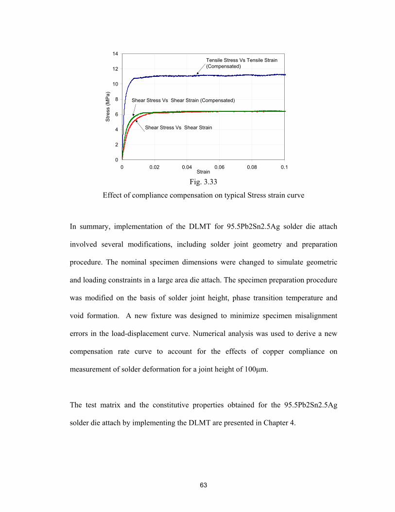
0
2
4
6
8
10
12
14
0 0.02 0.04 0.06 0.08 0.1Strain
Stre
ss (M
Pa)
Tensile Stress Vs Tensile Strain (Compensated)
Shear Stress Vs Shear Strain
Shear Stress Vs Shear Strain (Compensated)
Fig. 3.33
Effect of compliance compensation on typical Stress strain curve
In summary, implementation of the DLMT for 95.5Pb2Sn2.5Ag solder die attach
involved several modifications, including solder joint geometry and preparation
procedure. The nominal specimen dimensions were changed to simulate geometric
and loading constraints in a large area die attach. The specimen preparation procedure
was modified on the basis of solder joint height, phase transition temperature and
void formation. A new fixture was designed to minimize specimen misalignment
errors in the load-displacement curve. Numerical analysis was used to derive a new
compensation rate curve to account for the effects of copper compliance on
measurement of solder deformation for a joint height of 100µm.
The test matrix and the constitutive properties obtained for the 95.5Pb2Sn2.5Ag
solder die attach by implementing the DLMT are presented in Chapter 4.
63

Chapter 4. Constitutive Properties of 95.5Pb2Sn2.5Ag solder
4.1 Introduction
Monotonic, isothermal tests were conducted on 95.5Pb2Sn2.5Ag solder at constant
(shear) actual strain rates from 1x10⁻²s-1 to 1x10⁻⁶s-1 over a temperature range from
25oC to 150oC (0.5 to 0.75 homologous temperature) in strain control, to study the
effects of strain rate and temperature on the mechanical properties in a systematic
manner. The test matrix used in this study is shown in Figure 4.1 below:
Minimum Creep regime
Minimum Creep regime
Fig. 4.1
Test Matrix
The chosen solder alloy has a melting point of 304oC, however, the highest possible
temperature with the current configuration was 150oC, which permitted
experimentation at a maximum of 0.75 homologous temperature to obtain the
constitutive properties. The material characterized is highly compliant and the range
64

of strain rates chosen (1x10⁻²s-1 to 1x10⁻⁶s-1) was considered to be wide enough to
obtain time-independent plastic and time-dependent creep deformation. The stress-
strain behavior obtained at these temperatures and strain rates is plotted in Figures 4.2
through 4.5.
The flow stresses at corresponding strains were observed to be strong functions of
strain rate, with the stresses increasing with the strain rate due to less time for
thermally activated processes. Since thermally activated processes occurred faster at
higher temperatures, the stresses at corresponding strains were progressively lower at
150oC as compared to 25oC.
0
5
10
15
20
25
0 0.02 0.04 0.06 0.08 0.1Shear Strain
She
ar S
tress
(MP
a)
Strain Rate 1x10⁻⁴
Strain Rate 1x10⁻³
Strain Rate 1x10⁻²
25oC
Strain Rate 1x10⁻⁵
Strain Rate 1x10⁻⁶
Fig. 4.2
Stress-strain curves at 25oC
65

0
5
10
15
20
25
0 0.02 0.04 0.06 0.08 0.1Shear Strain
She
ar S
tress
(MP
a)
Strain Rate 1x10⁻²
Strain Rate 1x10⁻³
Strain Rate 1x10⁻⁴
Strain Rate 1x10⁻⁵
Strain Rate 1x10⁻⁶
80oC
Fig. 4.3
Stress-strain curves at 80oC
0
5
10
15
20
25
0 0.02 0.04 0.06 0.08 0.1Shear Strain
Shea
r Stre
ss (M
Pa)
Strain Rate 1x10⁻⁴
Strain Rate 1x10⁻³Strain Rate 1x10⁻²
Strain Rate 1x10⁻⁵
Strain Rate 1x10⁻⁶
125oC
Fig. 4.4
Stress-strain curves at 125oC
66

0
5
10
15
20
25
0 0.02 0.04 0.06 0.08 0.1Shear Strain
Shea
r Stre
ss (M
Pa)
Strain Rate 1x10⁻²
Strain Rate 1x10⁻³
Strain Rate 1x10⁻⁴Strain Rate 1x10⁻⁵
Strain Rate 1x10⁻⁶
150oC
Fig. 4.5
Stress-strain curves at 150oC
Using the above stress-strain curves, the dependencies of yield stress and ultimate
tensile strength on temperature and strain rate were obtained in addition to the
partitioned constitutive property measurements for the 95.5Pb2Sn2.5Ag solder alloy.
4.2 Yield Stress and Ultimate Tensile Strength
Yield stress and Ultimate tensile strength (UTS) were found to decrease with
temperature and increase with strain rate. Shi et al. [1999] made similar
extrapolations from their investigations with 63Sn/37Pb eutectic solder. Figures 4.6
and 4.7 show the dependency of yield stress on temperature and strain rate, and
figures 4.8 and 4.9 show the dependencies for ultimate tensile strength of
95.5Pb2Sn2.5Ag solder. The values for Yield stress obtained through testing are
shown in Table 4.1. The stress at 0.2% strain was taken as yield stress.
67

Yield Stress (MPa) Strain Rate (1/sec) 25oC 80oC 125oC 150oC
1x10⁻² 20.8 16.8 13.8 1.1
1x10⁻³ 18.7 15.3 11.8 9.6
1x10⁻⁴ 16.3 12.9 9.4 7.2
1x10⁻⁵ 13.5 10.8 7.9 5.5
1x10⁻⁶ 11.1 8.3 5.8 4.0
Table 4.1: Yield stress for 95.5Pb2Sn2.5Ag
1
10
100
25 80 125 150Temperature (oC)
Yie
ld S
tress
(MP
a)
1e-21e-31e-41e-51e-6
Fig. 4.6
Yield Stress of 95.5Pb2Sn2.5Ag as a function of temperature
68

1
10
100
1.00E-021.00E-031.00E-041.00E-051.00E-06Strain Rate (1/s)
Yie
ld S
tress
(MP
a)
25C80C125C150C
Fig. 4.7
Yield Stress of 95.5Pb2Sn2.5Ag as a function of strain rate
The above plots demonstrated that there was an approximately linear relationship
between the yield stress and temperature. However, it was evident that the yield stress
increased with strain rate in a non-linear manner. Two trends were visible. The slope
of each curve was slightly different at each temperature and increased with am
increase in temperature. The curve at 25oC was almost linear on the log-log plot and
became increasingly non-linear as test temperature was increased to 150oC. The other
trend was that the higher the temperature and the lower the strain rate, the greater was
the variation in yield stress. This was attributed to the fact that creep deformation
makes a larger contribution to the reduction in strength at higher temperatures and
lower strain rates.
The values obtained for UTS are shown in Table 4.2 below. The value corresponding
to the maximum stress in the stress-strain curve was taken as the UTS.
69

Ultimate Tensile Strength (MPa) Strain Rate (1/sec) 25oC 80oC 125oC 150oC
1x10⁻² 33.1 25.6 16.6 13.3
1x10⁻³ 28.3 20.6 13.3 10.9
1x10⁻⁴ 23.9 16.9 10.9 9.0
1x10⁻⁵ 19.4 13.6 8.8 6.8
1x10⁻⁶ 15.7 10.7 6.4 4.7
Table 4.2: Ultimate Tensile Strength for 95.5Pb2Sn2.5Ag
1
10
100
25 80 125 150Temperature (oC)
Ulti
mat
e Te
nsile
Stre
ngth
(MP
a)
1e-21e-31e-41e-51e-6
Fig. 4.8
Ultimate Tensile Strength of 95.5Pb2Sn2.5Ag as a function of temperature
70

1
10
100
1.00E-021.00E-031.00E-041.00E-051.00E-06Strain Rate (1/s)
Ulti
mat
e Te
nsile
Stre
ngth
(MP
a)
25C80C125C150C
Fig. 4.9
Ultimate Tensile Strength of 95.5Pb2Sn2.5Ag as a function of strain rate
The UTS showed an approximately linear relationship with temperature just as in the
case of yield stress. UTS also demonstrated a fairly linear relationship with strain rate
at lower temperatures, but the trend suggested a non-linear relationship at higher
temperatures and lower stain rates. A clearer picture may be obtained with tests
conducted at T>0.8Tm and 1x10⁻⁷ to 1x10⁻⁹ strain rates. This observation again
however, seemed to suggest creep deformation to be dominant at lower strain rates
and higher temperatures.
4.3 Time-independent Elasticity
The shear modulus of the solder alloy was determined by a combination of two
methods.
71

Method I
In the first method, 10 specimens were used to conduct monotonic, isothermal tests in
strain control at a constant (shear) actual strain rate of 1x10⁻³s-1 and at a constant
temperature of 25oC, for an extremely short duration of 2 seconds, to minimize the
influence of time-dependent (viscoplastic or anelastic) deformations on the results.
Ten such tests were repeated on each specimen without uninstalling it to account for
errors in measurement due to slippage of the specimen. The specimen was then
flipped over and the measurements were repeated. This accounted for errors
introduced in measurement due to misalignment of the machine grips. A force vs.
strain curve was plotted for each specimen for each run. Figure 4.10 shows one such
run for one specimen.
y = 65013x + 0.0573R2 = 0.9997
0
2
4
6
8
10
12
14
0 0.00005 0.0001 0.00015 0.0002 0.00025Strain
Forc
e (N
)
Force Vs Strain Linear (Strain Rate 10e-3)
Fig. 4.10
Sample force vs. Strain curve for specimen A1-10 at 25oC for
Method 1
72

73
The above plot clearly shows that the maximum value of the stress that the specimen
experienced during the test was well below the yield stress of the material, for the
corresponding strain rate, thus proving the validity of using such a test to measure
modulus. The slope of the curves obtained for all the specimens was averaged, since
there was a certain degree of scatter in the values from specimen to specimen. The
compliance effects of the copper specimen were accounted for in the manner
explained in section 2.5. The shear modulus was obtained from the ensuing force vs.
strain curve and the elastic modulus, E, was then obtained from the relationship,
)1(2 ν+=
EG
where G is shear modulus calculated from the slope of the force vs. strain plot curve,
and ν is the Poisson’s ratio (ν = 0.4 for pure lead).
For example, the calculation of elastic modulus at 25oC using method 1:
From force vs. strain curve for all specimens, averaged slope (S) = 52616N/ε.
Actual solder joint height (h) = 105.33µm.
Actual joint width (w) = 2.01mm.
Actual joint thickness (t) = 1.092mm.
Applied force (Fapp) = 26N.
Extensometer gauge length (l) = 3mm.
From Figure 3.32, compensation rate (CR [Cu]) = 4.69x10⁻⁸m/N, for t = 1.092mm.
From Equation (2.5), actual deformation of copper (δAB) = 1.22x10⁻⁶m.
(4.1)

74
Measured strain by extensometer ( BB ′ε ), at 26N = Fapp/S = 0.000494ε.
Measured deformation by extensometer ( BB ′δ ) = lBB ×′ε = 1.48x10⁻⁶m.
From Equation (2.6), actual deformation of solder (δAA`) = 2.63x10⁻⁷m.
Thus, shear stress (τ) = F/wt = 1.184x10⁷N/m2.
And shear strain (γ) = δAA`/h = 0.002497.
Shear Modulus (G) = τ/ γ = 4.744x10⁹N/m2 (Pa).
From Equation (4.1), Elastic Modulus (E) = 1.328x10¹⁰N/m2 (Pa), i.e. 13.28GPa.
Method II
In the second method, 13 specimens were used to conduct monotonic, isothermal tests
at 80oC, 125oC, and 150oC at a constant shear strain rate of 1x10⁻³s-1, to obtain shear
stress vs. strain curves as shown in Figures 4.2 through 4.5. The slope between the
origin and a point within the elastic regime of the stress vs. strain curve was used to
calculate the shear modulus, from which the elastic modulus was derived using
Equation (4.1), in a manner identical to method 1. A comparison between the two
methods showed a 5% difference in the slope, S. For example, Method I yielded an
average slope of 55345 at 25oC and a strain rate of 1x10⁻³s-1, and Method II an
average slope of 52456, for the same temperature and strain rate. This resulted in an
average Young’s Modulus of 13.49GPa from Method I and an average Young’s
Modulus of 13.06GPa from Method II, a difference of less than 5%. Method II was
used since it was possible to use the same data obtained from the constant strain rate
tests conducted for estimation of the time-independent plastic and time-dependent
creep properties for the estimation of Young’s Modulus of Elasticity, thereby

reducing the overall number of tests conducted. Table 4.3 shows the values of
Young’s modulii obtained through combined methods 1 and 2 for the whole range of
selected temperatures.
Young’s Modulus (G) GPa Temperature
(T) oC Maximum Average Minimum
25 14.61 13.28 12.10
80 10.46 9.27 8.35
125 8.40 7.34 6.42
150 7.19 5.81 4.27
Table 4.3: Elastic Modulus as a function of Temperature
Assuming a Poisson’s Ratio of 0.4 [Source: www.matweb.com], a modulus of
13.28GPa was found for the 95.5Pb2Sn2.5Ag solder at room temperature, which is
just lower than the modulus of pure lead (13.8GPa) [Source: www.matweb.com].
Figure 4.11 shows the dependence of elastic modulus on temperature. The elastic
modulus showed a linear relationship with temperature. As expected, the value of
Young’s modulus decreased with increase in temperature due to the increased
contribution of thermally activated processes such as creep deformation in reduction
of strength of the solder joint.
75

76
Fig. 4.11
Temperature dependence of elastic modulus, E
A modulus-temperature relationship for 95.5Pb2Sn2.5Ag solder alloy was obtained
for the average value of modulii:
)(0585.0448.30 KTE −=
The range of the modulus-temperature relationship was also obtained. The equations
(4.3) below show the modulus-temperature relationships for the obtained maximum
and minimum values of Young’s modulus:
)(0598.0099.32 KTE −=
)(0602.0915.29 KTE −=
(4.2)
(4.3)
y = -0.0602x + 29.915
y = -0.0598x + 32.099
0
2
4
6
8
10
12
14
16
18
20
280 300 320 340 360 380 400 420 440Temperature (K)
You
ng's
Mod
ulus
(GP
a)
Deviation Bands

While these expressions represented the test data fairly well, the combined effects of
the miniature specimen configuration, loading calibration effects, and the effects of
inelastic and thermally activated deformations on the apparent solder deformation
may well have had an effect on data interpretation. Thus, these results are
recommended for use only in durability modeling. The values of the elastic constants
obtained for Equation (2.10) are tabulated below:
Parameter Maximum Value Minimum
E0 32.099 30.448 29.915
ET 0.0602(T) 0.0585(T) 0.0598(T)
Table 4.4. Elastic constants
Figure 4.12 below shows the temperature dependence of Young’s Modulii of some
high lead solders, in comparison with that of the 95.5Pb2Sn2.5Ag solder.
0
5
10
15
20
25
30
275 300 325 350 375 400 425 450Temperature (K)
Youn
g's
Mod
ulus
(GPa
)
97Pb3Sn (Darveaux et al., 1992)
92.5Pb5Sn2.5Ag (Wilde et al., 2000)
97Pb3Sn (Wen et al., 2002)
95.5Pb2Sn2.5Ag (This study)97Pb3Sn (Cole et al., 1991)
Fig. 4.12
Temperature dependence of Young’s modulii of some lead-rich solders
77

It can be seen that the value of Young’s modulii reported by different investigators
differ even for alloys of the same composition. Several factors influence the
measurement of Young’s modulus including the loading rate, creep effects, specimen
configuration, and the structural compliance of the load train. The Table below shows
the values of Young’s modulii for some lead-rich solders at room temperature as
obtained by different investigators, as well as the assumed value of Poisson’s ratio.
Solder Specimen Type
Modulus at 25oC
Assumed Poisson’s ratio Source
92.5Pb5Sn2.5Ag Cylindrical dog-bone 23.32GPa 0.33 Wilde et al.,
2000
97Pb3Sn Flip-chip assembly 24.84GPa 0.35 Darveaux et
al., 1992
97Pb3Sn Cylindrical dog-bone 11.73GPa - Cole et al.,
1991
97Pb3Sn Cylindrical dog-bone 19.89GPa - Wen et al.,
2002
Table 4.5 Young’s Modulii for lead-rich solders obtained from literature
4.4 Time-independent Plasticity
To determine plastic constants for 95.5Pb2Sn2.5Ag solder, results from isothermal,
monotonic constant strain rate tests conducted on 54 specimens at actual shear strain
rates of 1x10⁻²s-1, 1x10⁻³s-1, 1x10⁻⁴s-1, 1x10⁻⁵s-1, and 1x10⁻⁶s-1, and temperatures of
25oC, 80oC, 125oC, and 150oC were used. Figure 4.13 is a plot of axial force vs. strain
for a constant strain rate test at 1x10⁻⁴s-1 and temperature of 25oC. These were
converted into shear stress vs. shear strain curves using the following relations,
78

79
wtF
=τ and lh
εδδγ == ;
where τ is the shear stress, F is the axial force, w is the joint width, t is the joint
thickness, γ is the shear strain, δ is the deformation of the solder joint, h is the joint
height, ε is the axial strain, and l is the gauge length of the extensometer. The
compliance effects of the copper specimen were accounted for in the manner
explained in section 4.2.
Fig. 4.13
Sample force vs. strain curve at a constant strain rate of 1x10⁻⁴ and
temperature of 25oC
As seen from figures 4.2 through 4.5, the flow stresses at corresponding strains were
strong functions of strain rate, with the stresses increasing with the strain rate due to
less time being allowed for thermally activated processes. Since thermally activated
processes occur faster at higher temperatures, the stresses at corresponding strains
were progressively lower at 150oC as compared to 25oC. Shear stress was converted
0
10
20
30
40
50
60
0 0.002 0.004 0.006 0.008 0.01 0.012Strain (micron)
Forc
e (N
)
Strain Rate 1x10e-04
(4.4)

80
to equivalent tensile stress and shear strain was converted to equivalent tensile strain
by applying the Von Mises yield criterion to obtain the relationships (repeated here
for continuity),
γετσ3
1,3 ==
Using the methodology explained in Section 2.7 for calculating the strain rate
independent stress, six values of strain were chosen for which the corresponding flow
stress would be extrapolated, namely 0.5%, 0.75%, 1%, 2.5%, 5%, and 7.5%. Stress
vs. strain rate curves were plotted for these values of strain, for each temperature.
Figure 4.14 shows such a plot for 125oC.
Fig. 4.14
Equivalent stress vs. strain rate plot for the chosen values of strain for converted
strain rates of 1x10⁻²s-1 through 1x10⁻⁶s-1 and temperature of 125oC
(2.15)
y = 0.4816Ln(x) + 13.045
y = 0.5068Ln(x) + 13.938
y = 0.6089Ln(x) + 15.344
y = 0.3752Ln(x) + 14.028
y = 0.7079Ln(x) + 16.675
y = 0.813Ln(x) + 17.919
0
2
4
6
8
10
12
14
16
0.000 0.001 0.002 0.003 0.004 0.005
Strain Rate (s-1)
Stre
ss (M
pa)

A logarithmic curve was observed to provide the best fit to the test data. The values
of equivalent stress obtained from the curve fit were extrapolated for very high strain
rates. For this purpose the unrelaxed stress was defined as the value corresponding to
the point where the slope of the extrapolated curve fell below 10-3MPa-s. This rate-
independent equivalent stress was then plotted against equivalent strain yielding a
rate-independent stress vs. strain curve for each temperature. Figure 4.15 shows such
rate-independent stress vs. strain plots for the whole selected range of temperatures.
0
10
20
30
40
50
60
0 0.01 0.02 0.03Te
Tens
ile S
tress
(MP
a)
298K353K398K423K
s
F
Strain rate-independent equivalent
A power law described in chapter 2 gi
curves to obtain the constants np and K,
the pre-exponential co-efficient respec
Deviation Bar
0.04 0.05 0.06 0.07 0.08nsile Strainig. 4.15
tensile stress vs. equivalent tensile strain
ven by Equation (2.11) was fit to the above
which are the strain hardening exponent and
tively. The values of the plastic constants
81
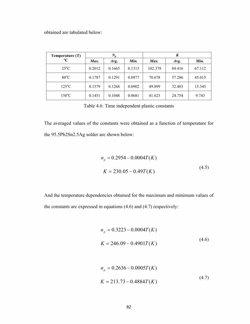
82
obtained are tabulated below:
Np K Temperature (T) oC Max. Avg. Min. Max. Avg. Min.
25oC 0.2012 0.1665 0.1313 102.378 84.416 67.112
80oC 0.1787 0.1291 0.0977 70.678 57.286 45.015
125oC 0.1579 0.1268 0.0902 49.899 32.403 15.345
150oC 0.1451 0.1048 0.0681 41.623 24.754 9.743
Table 4.6: Time independent plastic constants
The averaged values of the constants were obtained as a function of temperature for
the 95.5Pb2Sn2.5Ag solder are shown below:
)(0004.02954.0 KTnp −=
)(49.005.230 KTK −=
And the temperature dependencies obtained for the maximum and minimum values of
the constants are expressed in equations (4.6) and (4.7) respectively:
)(0004.03223.0 KTnp −=
)(4901.009.246 KTK −=
)(0005.02636.0 KTnp −=
)(4884.073.213 KTK −=
(4.5)
(4.6)
(4.7)

Their respective temperature dependencies are plotted below in Figures 4.16 and
4.17.
y = -0.0004x + 0.3223
y = -0.0005x + 0.2636
0
0.04
0.08
0.12
0.16
0.2
0.24
0.28
280 300 320 340 360 380 400 420 440Temperature (K)
Stra
in H
arde
ning
Exp
onen
t, np
Deviation Bands
Fig. 4.16
Temperature dependence of strain hardening exponent
Fig. 4.17
Temperature dependence of pre-exponential co-efficient
y = -0.4884x + 213.73
y = -0.4901x + 246.09
0
20
40
60
80
100
120
280 300 320 340 360 380 400 420 440Temperature (K)
Pre
-Exp
onen
tial C
oeffi
cien
t, K
Deviation Bands
83

A reasonable fit was obtained for the test data. Both the strain hardening exponent
and the pre-exponential co-efficient decreased with increasing temperature, since at
higher temperatures, thermally activated processes such as creep deformations could
induce stress relaxation thereby reducing the strength of the joint. However, it should
be noted that the contribution of time-independent plastic deformation to the total
deformation of lead-rich solders is negligibly small. Therefore, even a small amount
of variation in the acquired data may cause a relatively large change in the value of
the time-independent plasticity constants.
4.5 Time-dependent Steady-state Creep
In a constant strain rate test, after the strain or loading time is sufficient, the strain
hardening is nearly zero when the plastic flow reaches a steady state. Furthermore,
the stress and deformation resistance are approximately the saturation values [Wilde
et al., 2000]. This is analogous to the steady state saturation strain rate for a constant
load/stress test [Zhang et al., 2003]. Thus, even from these experiments one can
calculate the steady state strain rate and saturation stress pairs. Saturation stress was
observed to be temperature and strain rate dependent.
84

85
Data from 54 specimens subjected to monotonic, isothermal, constant strain rate tests
for a wide range of temperatures of 25oC, 80oC, 125oC, and 150oC, and strain rates of
1x10⁻²s-1, 1x10⁻³s-1, 1x10⁻⁴s-1, 1x10⁻⁵s-1, and 1x10⁻⁶s-1 was used to model the time
dependent plastic behavior that is creep. The saturation stress value was calculated for
each strain rate and temperature. The results are summarized in table 4.7 below:
τ (Mpa)
T = 298K T = 298K T = 298K T = 298K dγ/dt
Max Avg Min Max Avg Min Max Avg Min Max Avg Min
1.00x10⁻² 20.5 19.1 18.0 15.7 14.8 13.9 10.1 9.60 9.03 8.42 7.70 6.96
1.00x10⁻³ 17.3 16.4 15.3 12.8 11.9 11.1 7.77 7.31 6.89 6.76 6.31 5.82
1.00x10⁻⁴ 14.6 13.8 13.1 9.98 9.36 8.85 6.83 6.29 5.93 5.64 5.21 4.86
1.00x10⁻⁵ 11.5 10.6 9.78 8.51 7.84 7.18 5.21 4.90 4.58 4.31 3.96 3.56
1.00x10⁻⁶ 9.78 9.07 8.34 7.10 6.50 5.93 4.35 3.99 3.67 3.60 3.19 2.80
Table 4.7: Saturation stress and strain rate pairs for different temperatures
These results were then converted to the equivalent tensile creep strain rate and
corresponding equivalent tensile stress using equation (2.15) derived from Von
Mises’ yield criteria, and then plotted on a natural log-log scale as shown in Figure
4.18.

86
Fig. 4.18
Log-log plot of equivalent steady state creep strain rate and equivalent average
saturated stress pairs
The slope of the strain rate vs. average saturated stress curves for different
temperatures yielded the creep exponent and the intercept yielded the stress co-
efficient and the thermal activation energy for creep, and was calculated as follows
(repeated here for continuity),
vc
cr nRTQA σε ln1lnln +−=&
The parameters thus calculated for the whole range of temperatures are summarized
in the table below:
-50
-40
-30
-20
-10
0
10
0 1 2 3 4 5
298K353K398K423K
(2.16)
lnσvlnσv

87
cn1
RTQA −ln
Temperature (T)
Max Avg Min Max Avg Min
25oC (298K) 12.312 11.848 11.421 -49.932 -46.910 -43.899
80oC (353K) 11.490 11.123 10.673 -44.657 -41.094 -38.454
125oC (398K) 11.189 10.671 10.113 -37.823 -34.975 -32.720
150oC (423K) 10.823 10.308 9.814 -35.374 -32.061 -29.278
Table 4.8: Creep model parameters calculated from log-log plot
These parameters were then used to obtain their corresponding temperature
dependency relationships from the plots shown in Figures 4.19 and 4.20. The
obtained relationships are given by the equations,
)(0121.0425.151 KTnc
−=
)(149034661.2)(ln KTRTQA −=−
The temperature dependencies of the maximum and minimum values of the
parameters were also obtained as shown below in equations (4.9) and (4.10)
respectively:
)(0116.067.151 KTnc
−=
)(139962162.3)(ln KTRTQA −=−
(4.8)
(4.9)

88
)(0128.0211.151 KTnc
−=
)(154542514.1)(ln KTRTQA −=−
Fig. 4.19
Temperature dependence of creep exponent
Fig. 4.20
Arrhenius plot to determine creep thermal activation energy
y = -0.0116x + 15.67
y = -0.0128x + 15.211
8
9
10
11
12
13
14
260 310 360 410 460Temperature (K)
Cre
ep S
train
Har
deni
ng E
xpon
ent
Deviation Bands
(4.10)
y = -15454x + 1.2514
y = -13996x + 3.2162
-60
-50
-40
-30
-20
0.0021 0.0025 0.0029 0.0033 0.00371/T (1/K)
lnA
-Q/R
T Deviation Bands

The stress co-efficient, A, was calculated from the y-intercept of the average curve in
Figure 4.20, and the thermal activation energy, Q, was calculated from the slope of
the same curve. The values are shown in Table 4.9 below:
Values Parameter
Max Avg Min
A 24.933 11.776 3.495
Q 1.33eV 1.28eV 1.21eV
Table 4.9: Time dependent creep constants
The average value of the creep stress exponent that was obtained suggested
dislocation climb controlled deformation. The average value of activation energy that
was obtained is very close to that of lattice diffusion in pure lead (1.1eV). This is
somewhat inconsistent with the obtained stress exponent. The probable reasons for
this behavior are discussed in detail in section 4.6 below.
4.6 Discussion
Under shear loading, most solder alloys show a decrease in ductility as temperature is
increased or strain rate is decreased [Darveaux et al., 1992]. This observation is
consistent with a strain energy partitioning approach to cyclic fatigue damage, where
the intent is to separately quantify damage due to elastic potential energy, plastic
work and creep work. Typically, creep is considered significantly more damaging.
Thus this section is devoted to understanding the mechanisms of creep deformation.
89

A creep deformation mechanism map for steady-state (secondary) creep is shown in
Figure 4.21 [Frost et al., 1982], where the stress is normalized by the shear modulus.
Fig. 4.21
Simplified creep deformation mechanism map
Lattice diffusion creep represents a creep mechanism controlled by atomic diffusion
under application of very low stress and is usually called Nabarro-Herring creep
[Dieter, 1986]. Usually, a stress not high enough to move dislocations but enough to
trigger atoms or vacancies to migrate in preferential directions if T > 0.5Tm (high
homologous temperatures) causes lattice diffusion. At relatively higher stress and low
homologous temperature (T<0.5Tm), lattice diffusion becomes progressively difficult.
In this case, atoms or vacancies move easily in porous grain boundaries, since they
less closely packed along the grain boundaries. This is known as grain boundary
diffusion or core diffusion. At high stress levels and high homologous temperatures,
creep rate is controlled by dislocation motion, causing deformation known as
dislocation creep or dislocation climb. Dislocations in crystalline materials are
activated to glide at the highest stresses. If other dislocations, precipitates or phase
particles obstruct motion of the dislocations, then dislocation climb helps the
90

dislocations to continue gliding. In this case, gliding produces all the creep strain,
while climbing controls the creep rate, since atomic diffusion controls climbing and
the gliding rate is much faster than the diffusion rate. At intermediate values of stress
and higher homologous temperatures, grain boundary (GB) sliding or superplasticity
is known to occur. Here grains shear with respect to each other at the grain
boundaries. The characteristic behavior of steady-state creep deformation kinetics of
solder alloys at high homologous temperatures is shown schematically in Figure 4.22.
Fig. 4.22
Schematic of log-log plot of shear creep rate vs. applied shear stress (for steady state
creep deformation of metals and alloys at high homologous temperatures [Hacke et al., 1997])
Regions I and II are grain (phase) size dependent whereas regions III and IV are not.
Generally, investigators have focused their research on regions II and III, deformation
within which is dominated by grain boundary sliding (superplasticity) and dislocation
climb (matrix creep) respectively. Grivas et al. suggested that Pb-Sn eutectic alloys
exhibit both superplasticity and matrix creep, simultaneously occurring through
independent mechanisms. Superplasticity is rate controlling at lower stresses whereas
matrix creep is rate controlling at higher values of stress [Schubert et al., 2001].
Stress exponents and activation energies found by various investigators using various
91

test specimens and methodologies for Pb-based solder materials are shown in Table
4.10 for comparison.
Solder alloy Specimen Type Model Stress
Exponent Activation
Energy (eV) Creep
Mechanism Investigator
92.5Pb5Sn2.5Ag Cylindrical dog-bone Anand Model - 0.95 Lattice diffusion Wilde et al.,
2000
92.5Pb5Sn2.5Ag BGA solder joint
Creep power-law (low temp/
high temp) 11.59/8.34 - Dislocation climb Solomon,
1990
98Pb2Sn Rectangular tensile
Weertman (high temp) 8.0 0.99 Lattice diffusion Frost et al.,
1988
98Pb2Sn Rectangular tensile
Weertman (low temp) 13.0 0.46 Dislocation climb Frost et al.,
1988
97Pb3Sn Flip-chip assembly
Modified hyperbolic sine 7.0 1.20 Dislocation climb Darveaux et
al., 1992
96.5Pb3.5Sn Cylindrical dog-bone Weertman 13.0 0.75 Dislocation climb Wen et al.,
2002
96.5Pb3.5Sn Rectangular tensile
Weertman (high temp) 5.0 0.99 Lattice diffusion Frost et al.,
1988
96.5Pb3.5Sn Rectangular tensile
Weertman (low temp) 6.5 0.62 Dislocation climb Frost et al.,
1988
95Pb5Sn Flip-chip assembly
Modified hyperbolic sine 7.0 1.20 Dislocation climb Darveaux et
al., 1992
95Pb5Sn Rectangular tensile
Weertman (high temp) 7.0 0.67 Lattice diffusion Frost et al.,
1988
95Pb5Sn Rectangular tensile
Weertman (low temp) 7.0 0.62 Dislocation climb Frost et al.,
1988
90Pb10Sn Rectangular tensile
Weertman (high temp) 5 0.67 Lattice diffusion Frost et al.,
1988
90Pb10Sn Rectangular tensile
Weertman (low temp) 3.0 0.62 Dislocation climb Frost et al.,
1988
63Sn37Pb Actual solder assemblies
Partitioned creep 2.0/7.1 0.5/0.84 GB sliding/
matrix creep Grivas et al.,
1979
63Sn37Pb Actual solder assemblies
Partitioned creep 1.7/11.1 0.46/1.0 GB sliding/
matrix creep Kashyap et al., 1981
63Sn37Pb - Partitioned creep 3.1/7.3 - GB sliding/
matrix creep Solomon,
1986
63Sn37Pb Actual solder assemblies
Partitioned creep 2.4/5.7 0.45/0.9 GB sliding/
matrix creep Lam et al.,
1979
63Sn37Pb - Partitioned creep 3.0/7.0 0.47/0.47 GB sliding/
matrix creep Wong et al.,
1988
63Sn37Pb Cylindrical dog-bone
Modified hyperbolic sine 5.0/3.0 0.5/0.84 Dislocation glide/
lattice diffusion Shi et al.,
2001
63Sn37Pb Cylindrical dog-bone
Weertman-Dorn 2.0/7.1 0.5/0.84 GB sliding/
matrix creep Hacke et al.,
2001
62Sn36Pb2Ag Flip-chip assembly
Modified hyperbolic sine 3.3 0.55 Dislocation
viscous glide Darveaux et
al., 1992
60Sn40Pb Flip-chip assembly
Modified hyperbolic sine 3.3 0.55 Dislocation
viscous glide Darveaux et
al., 1992
59Sn40Pb1Ag Cylindrical dog-bone
Weertman-Dorn 1.87/6.74 0.5/0.79 GB sliding/
matrix creep Schubert et
al., 2001
Table 4.10: Comparison of creep model parameters obtained from literature
92

As observed in the table on the previous page, there is a marked difference in values
of activation energy and stress exponent as observed by different investigators. There
are several factors contributing to the large variation in measured parameters,
including type of specimen, geometry and loading constraints of specimen/solder
joint, the specimen preparation procedure and conditioning (aging), resulting
microstructure and grain size of the alloy, intermetallic compound formation, type of
test and manner in which it was conducted, temperatures and strain rates used,
measurement calibration and accuracy (gauge length), modeling methodology used to
fit experimental data, and underlying assumptions of mechanical properties of
material, such as shear modulus and Poisson’s ratio. Furthermore, the stress exponent
is larger in the high stress regime than it is in the lower stress regime at any given
temperature. This phenomenon is known as power-law breakdown. The activation
energy if determined from different points on one single curve can be different for the
same stress level [Shi et al., 2001].
Often, more than one creep mechanism operates simultaneously. If several
mechanisms are mutually dependent, the fastest mechanism governs the creep
behavior, while if the mechanisms act independently, then the slowest mechanism
governs the creep behavior [Li et al., 1993]. Thus, even though the deformation
mechanism responsible for the creep deformation may be dislocation climb as
indicated by the high stress exponent, the deformation rate is governed by the atomic
lattice diffusion. Further testing conducted at lower shear strain rates of 1x10⁻⁷s-1 to
93

94
1x10⁻⁹s-1 and temperatures upto 200oC may provide some clarifications. As a
representative result, Figure 4.23 shows the comparison of experimental data and the
prediction from the Weertman Model.
vσln
Fig. 4.23
Comparison of model prediction and experimental data for steady-state creep
behavior
A good agreement between the experimental data and the model predictions was
achieved for the assumed test conditions. Some deviations from the experimental data
and model predictions were observed as expected: the model consistently
underestimated the stresses at 80oC, and slightly overestimated the stresses at 150oC
compared with experimental data. Nevertheless, the model represented the creep
deformation behavior quite well.
-20
-18
-16
-14
-12
-10
-8
-6
-4
-2
0
1 2 3 4
298K - Experiment353K - Experiment398K - Experiment423K - ExperimentModel Prediction

Conclusions
Components of a power electronic device, including the die attach experience
operating temperatures as high as 200oC, which may cause significant reliability
concerns. The common eutectic Sn-Pb solder cannot fulfill these service
requirements, and one must turn to solder alloys with higher melting points such as
the Pb-rich alloys, which have a melting point in the range of 300oC. Before the
reliability of any system can be accurately predicted for the field conditions, one has
to be able to accurately predict the reliability of critical components of the system,
once they have been identified. The die attachment material of a power electronic
device is one of the weak links in the system. Durability characterization is essential
in order to accurately predict the reliability of the solder alloy chosen for the die
attach material under life cycle loads. However, relevant constitutive property
measurements must be carried out, as these are essential for quantitative
characterization of damage accumulation, the knowledge of which is essential for
accurate durability assessment.
The solder chosen for constitutive measurements is one of the commonly used high
temperature solders, namely the 95.5Pb2Sn2.5Ag solder alloy. Constitutive property
measurements of 95.5Pb2Sn2.5Ag solder have been conducted by adapting an
existing specimen configuration and test methodology developed for constitutive
property measurements of lead-free solder alloys used as controlled collapse chip
connection (C4) in small signal electronic devices.
95

A specimen with a solder joint of nominal dimensions 2mm x 1.5mm x 100µm
designed to simulate geometrical and loading constraints in a die attach was utilized
for testing on a uniaxial MTS TytronTM 250 Microforce testing machine. The
specimen preparation procedure was improved to obtain optimum solder joint quality
before commencement of testing to enhance repeatability of test data.
Monotonic, isothermal tests were conducted at constant shear strain rates of 1x10⁻²s-1,
1x10⁻³s-1, 1x10⁻⁴s-1, 1x10⁻⁵s-1, and 1x10⁻⁶s-1, and at temperatures of 25oC, 80oC,
125oC, and 150oC to obtain the temperature and strain rate dependent mechanical
properties such as Yield stress and Ultimate tensile strength, as well as the time-
independent elastic and plastic, and the time-dependent creep constitutive properties
of the solder alloy.
A partitioned constitutive approach was chosen for modeling purposes. The material
specific parameters of the models were extrapolated from the experimental data by
suitably curve fitting the data, and reasonable fits were obtained. Special attention
was given to creep deformation, since for solder alloys creep deformations contribute
most of the damage accumulated during cyclic fatigue at high homologous
temperatures. Diffusion mechanisms for creep deformation were discussed and the
diffusion mechanism(s) responsible for creep deformation in 95.5Pb2Sn2.5Ag solder,
for the given test conditions, was (were) identified. The creep model predictions were
then compared with the experimental data, and a good agreement was achieved.
96

Contributions
1. First program to employ the MTS TytronTM 250 Tester for measuring mechanical
properties of ternary 95.5Pb2Sn2.5Ag solder alloy used as die attach in high
temperature and high power applications.
2. First implementation of a direct local strain measurement technique (DLMT)
developed by Kwon et al. [2003] for constitutive property measurement of lead-
free solder alloys using the MTS TytronTM 250 Tester, for measuring the
constitutive properties of 95.5Pb2Sn2.5Ag solder.
a. Customized a miniature modified Iosipescu single-lap micro-shear
specimen designed for simulating geometrical and loading constraints
of a C4 joint in SMT, to simulate the constraints present in a large area
die attach used in power packaging, by suitably altering the solder
joint geometry.
b. Modified the specimen preparation procedure to account for
differences arising due to joint height and phase transition temperature.
c. Obtained temperature and strain rate-dependent mechanical properties
for 95.5Pb2.Sn.25Ag solder alloy such as Yield stress and Ultimate
tensile strength.
d. Determined the partitioned time-independent elastic, time-
independent-plastic, and the time-dependent creep properties for a
range of temperatures and strain rates.
97

98
Appendix A - Testing Procedures Using MTS TytronTM 250
A.1 Machine Pre-start Instructions
To start operating the machine, the station manager must first be invoked.
• Select the MTS Teststar® icon on the PC desktop.
• Open the Station Manager – A dialog window titled open station appears.
• Use any existing configuration and choose a parameter set, or create a new
configuration and define new user specific parameter set (consult Model
793.10 MutiPurpose TestWare manual).
Safety goes hand in hand with the operation of any machine and the Tytron is no
exception. It is highly recommended that one follow this pre-start checklist before
switching on the machine and operating it.
• Read the available Manuals-
o Tytron 250 Microforce Test System (Hardware)
o Model 793.10 MutiPurpose TestWare
o Controller Installation and Calibration
o Model 793.00 Software Installation
o Axial Extensometer Product Information
o System Software
• Check all cable connections-
Consult the installation manual, and check if all the cable connections
between the machine, the digital controller, the amplifier, and the PC,

99
including the ethernet cable connection, are correctly in place.
• Load or re-load the TestStar IIs digital software-
If the service light is on, the TestStar IIs system software must be re-loaded
before the machine can be operated.
• Locate and connect the Emergency Interlock device (Remote Station Control)-
This device allows the operator to switch off the machine in case of any
emergency, with the push of a single button.
• Choose the correct force transducer to install-
Install the 250N or 10N load cell and corresponding cable depending on
application.
• Check Air supply-
Before switching on the machine, make sure that the air supply is on, and the
air pressure is 100psi.
• Install actuator runaway protector-
This is a small fixture, which fits into the T-slot on the test bed. It protects the
force transducer by stopping the actuator in the case of runaway.
• Install temperature chamber-
Install if required, along with the heating ducts and water pipes for keeping
the remaining components of the machine cool. Turn on water supply. Use
long grips for high temperature configuration.
• Ensure that machine is switched on only in displacement control-
This is extremely important since the machine is started without loading the
specimen and there is no protection against impact with the force transducer in

100
case of actuator runaway. Displacement control ensures that the actuator
motion is restricted.
• Set all appropriate interlocks-
Check for the maximum and minimum values for displacement, force and
strain, and set appropriate interlocks.
• Keep hands clear of the path of the actuator at al times-
The actuator speeds can be very high and body parts that come in the way of
the actuator can be crushed against the reaction fixture.
A.2 Tuning
The machine requires tuning values for each control mode viz. displacement, force,
strain and temperature for each new specimen material and geometry before
commencement of actual testing. These tuning values are a distinct set of PID
(proportional-integral-derivative gains) values for the chosen cyclic frequency of
oscillation. These PID values can be manipulated using given controls and the
response of the machine is measured through the oscilloscope. The aim is to make the
mean, amplitude, peak, and valley of the measurable output value be as close to the
desired output value of displacement, force, or strain, at the same time keeping the
error down to a minimum, for a particular input value of displacement, force, or
strain. Tuning values for the 95.5Pb2Sn2.5Ag solder are shown in Table A.1.

101
Tuning Mode Device P I D Displacement ±60mm range
(w/o specimen) LVDT 1.75 1.85 0.042
Force ±250N Transducer 1.00 2000.00 0.001
Displacement ±5mm range LVDT 1.20 3400.00 0.001
Strain 8% range Extensometer 2.00 50000.00 0.001
Table A.1: Tuning Values for 95.5Pb2Sn2.5Ag solder micro-shear lap specimen
A.2.1 Displacement Mode Tuning Without Specimen
The machine must first be tuned without the installation of any specimen, with just
the grips or clamps in place. This ensures that the machine is in stable operating
condition when the actuator is first switched on. The following steps should be
followed for displacement tuning without installation of specimen:
• Set Target Set-point=0.00mm; Amplitude=2mm; Frequency=1Hz in the
Function Generator of the Station Manager.
• Set privilege level to Tuning from the drop down list on the Station Manager
window (password- Tuning; case-sensitive).
• In the Station Set-up window, go to //station/channels/axial/displacement/. In
Channel input signals set the Current Range to ±60mm for Displacement.
• Set the limits as ±20mm and set the Manual Offset in Offset-zero to zero.
• Select the manufacturer specified initial tuning values of P=1.0, I=0.1 &
D=0.001 in Channel Tuning.
• Set the Meters to give Timed, Mean/Amplitude, and Peak/Valley values for
Displacement. Select appropriate units.

102
• Switch the machine on by clicking on the HSM1 button on the Station
Manager. If the machine becomes unstable at any point of time (rapid
vibrations/oscillations), press the red button on the Remote station control
immediately.
• Click on the button for Manual Control in the Manual Command window to
enable Manual Command.
• Set Manual Command Displacement to Zero.
• Disable Manual Command.
• Set Signal Auto Offset as zero for displacement, force and strain.
• Set the parameters for the Scope: Control Channel – Axial; Control Signal –
Displacement; Response Signal – Axial; Response Signal – Error; and then
Re-scale.
• Switch on the Function Generator by depressing the PLAY button.
• The actuator will oscillate with the specified Target Set-point, Amplitude,
Frequency and Range, according to the selected PID gain values.
• The command displacement signal will be a Triangular wave in red and error
signal should be a Square wave in blue if the selected waveform in Station
Manager is Ramp.
• Now alter PID values slowly to match the output displacement for the timed,
mean/amplitude and peak/valley values with the command input values, and
to minimize the error value, to consequently obtain reasonably good
waveforms. Make a note of PID values obtained.
• Never set PID values to zero; machine will become unstable.

103
• Never drag the cursor to change the PID values.
• Stop the function generator.
A.2.2 Force Mode Tuning With Specimen
• Continuing from the previous section, go the Station Set-up window to
//station/channels/axial/force/ without switching off the machine. In Channel
input signals set the Current Range to ±250N and set the Manual Offset in
Offset-zero to zero.
• Set the limits as ±200N and set the Manual Offset in Offset-zero to zero.
• Set the values of P=1.0, I=0.50 & D=0.001 in Channel Tuning.
• Set Target Set-point=6N; Amplitude=4N; and Frequency=1Hz.
• Install the specimen between the grips. Do not clamp down.
• Enable Manual Command. Change the control mode to Force in the Manual
Command.
• Tighten the clamps with the magnetic clamp support mounted in place so as to
avoid breaking the specimen due to bending of the axis.
• Change the parameters in the Meters to give Timed, Mean/Amplitude, and
Peak/Valley display for Force instead of displacement.
• Similarly, set the control signal to Force in Scope and re-scale.
• Set Force to zero in Manual Command.
• Set Signal Auto Offset as zero for displacement, force and strain.
• Start the Function generator.

104
• Now alter PID values slowly to match the output force for the timed,
mean/amplitude and peak/valley values with the command input values, and
to minimize the error value, to consequently obtain reasonably good
waveforms. Make a note of PID values obtained.
• Stop the function generator.
A.2.3 Displacement Mode Tuning With Specimen
• Continuing from previous section, in the Station Set-up window, go to
//station/channels/axial/displacement/. In Channel input signals set the
Current Range to ±5mm for Displacement.
• Set the limits as ±2mm. DO NOT set the Manual Offset in Offset-zero to zero.
• Set the values of P=1.00, I=0.50 & D=0.001 for displacement in Channel
Tuning.
• Change the control mode back to displacement in function generator.
• Set Target Set-point=0.01mm; Amplitude=0.01mm; Frequency=1Hz.
• Enable Manual Command.
• Change the control mode in Manual Command to displacement.
• DO NOT SET Manual Command Displacement to zero.
• Disable Manual Command.
• Set Signal Auto Offset as zero.
• Change the parameters in the Meters to give Timed, Mean/Amplitude, and
Peak/Valley display for displacement instead of Force, using appropriate
units.

105
• Similarly, set the control signal to Displacement in Scope and re-scale.
• Start the function generator.
• Now alter PID values slowly to match the output displacement for the timed,
mean/amplitude and peak/valley values with the command input values, and
to minimize the error value, to consequently obtain reasonably good
waveforms. Make a note of PID values obtained.
• Stop the function generator.
A.2.4 Strain Mode Tuning With Specimen
• Ensure that the extensometer is securely attached to the specimen.
• Continuing from previous section, in the Station Set-up window, go to
//station/channels/axial/strain/, without stopping the machine. In Channel
input signals set the Current Range to ±8.0% for Strain.
• Set the limits as ±8.0%. DO NOT set the Manual Offset in Offset-zero to zero.
• Set the values of P=1.00, I=0.50 & D=0.0001 for strain in Channel Tuning.
• Change the control mode to strain in function generator.
• Set Target Set-point=100µε; Amplitude=100µε; Frequency=1Hz.
• Enable Manual Command.
• Change the control mode in Manual Command to strain. DO NOT SET
Manual Command strain to zero.
• Disable Manual Command.
• Set Signal Auto Offset as zero.

106
• Change the parameters in the Meters to give Timed, Mean/Amplitude, and
Peak/Valley display for strain, using appropriate units.
• Set the control signal to Strain in Scope and re-scale.
• Start the function generator.
• Now alter PID values slowly to match the output strain for the timed,
mean/amplitude and peak/valley values with the command input values, and
to minimize the error value, and consequently obtain reasonably good
waveforms.
• Stop the function generator.
• Stop the machine.
• Return the control mode to Displacement in Manual Command and in
Function generator.
• Save the PID values obtained for displacement, force, and strain modes for the
new specimen in a logbook.
• Remember to follow pre-start instructions next time the machine is operated.
A.3 Measurement Calibration
The MTS TytronTM is a uni-axial testing machine. The force transducer measures
axial force and the miniature extensometer measures axial strain. In order to apply a
particular shear strain rate on the solder joint during any experimental run, the
machine must be instructed to apply a corresponding actuator (crosshead) axial strain
rate.

107
For example, to convert a shear strain rate of 1x10⁻⁵s-1 to the corresponding axial
strain rate, the following procedure is followed:
Desired actual shear strain rate (dγ/dt): 1x10⁻⁵s-1
Solder Joint Height (h): 106.33µm
Gauge length (l): 3mm
Back-calculated actuator axial strain rate (dε/dt):
dtd /ε 1000
)/(×
=l
hdtdγ
( )10003
33.106101 5
××= −
171054433.3 −−×= s
Thus to apply an actual shear strain rate of 1-5101 −× s on the solder joint, the machine
is instructed to apply an axial strain rate of 171054433.3 −−× s . Figure A.1 serves to
validate that the back-calculated actuator axial strain rate applied by the machine is
correct as calculated.
(3.1)

108
Fig. A.1
Applied actuator axial strain rate
A.4 Constant Strain Rate Test Procedure
During any test, instructions are conveyed to the machine through a stored procedure.
Usually, the control mode, the absolute end-level of the applied load, the temperature,
the data acquisition time, the various output parameters to be monitored, and the
name and location of the output files is specified in these procedures. The data
acquisition time is particularly important. For a higher shear strain rate of say, 1x10-
1s-1, the data acquisition time must be very short, to ensure that sufficient data points
are gathered in order to obtain a smooth stress-strain curve. However, for a low shear
strain rate of say, 1x10⁻⁶s-1, one must exercise caution so as to not exceed the
resolution of the extensometer (2.44µε for 8.0% strain range). Table A.2 shows the
data acquisition times used for the different shear strain rates.
y = 3.5443E-07x + 2.8666E-06R2 = 1.0000E+00
0
0.005
0.01
0.015
0.02
0.025
0.03
0 20000 40000 60000 80000Time (sec)
Bac
k-ca
lcul
ated
act
uato
r stra
in ra
te (s
-1)

109
Actual shear strain rate (s-1)
Data acquisition time (sec)
Minimum resolution
required (µε)
Extensometer resolution (µε)
1x10⁻² 0.01 3.75 2.44
1x10⁻³ 0.1 3.75 2.44
1x10⁻⁴ 1.0 3.75 2.44
1x10⁻⁵ 10.0 3.75 2.44
1x10⁻⁶ 100.0 3.75 2.44 Table A.2: Data Acquisition times for different strain rates
For example, a constant strain rate test conducted on a specimen with a solder joint
height of 106.33µm, at an actual shear strain of 1x10⁻⁵s-1 and 125oC, will have the
following essential specifications:
Test Type: Ramp
Channel: Axial
Control Mode: Strain
Duration: 1000000sec
Absolute End level: µε33.35443310000001054433.3 17 =×× −− s (from section 3.3.3)
Channel: Temperature: 125oC
Data acquisition time: 10sec
Output values: Axial force, axial strain, time, and temperature
Once the procedure has been stored, the following steps will assist in conducting a
typical constant strain rate test. Remember to follow all pre-start instructions.

110
• In the Station Set-up window, go to //station/channels/axial/displacement/. In
Channel input signals set the Current Range to ±60mm for Displacement.
• Set the limits as ±20mm and set the Manual Offset in Offset-zero to zero.
• Select tuning values of P=1.75, I=1.85 & D=0.042 in Channel Tuning.
• In the Station Set-up window, go to //station/channels/axial/force/. In Channel
input signals set the Current Range to ±250N for Force.
• Set the limits as ±200N and set the Manual Offset in Offset-zero to zero.
• Select tuning values of P=1.0, I=2000.0 & D=0.001 in Channel Tuning.
• In the Station Set-up window, go to //station/channels/axial/strain/. In Channel
input signals set the Current Range to ±8.0% for Strain.
• Set the limits as ±8.0% and set the Manual Offset in Offset-zero to zero.
• Select tuning values of P=2.0, I=50000.0 & D=0.001 in Channel Tuning.
• Set the Meters to give Timed, Mean/Amplitude, and Peak/Valley values for
Displacement, strain, and force. Select appropriate units.
• Switch on temperature controller and set desired temperature in manual
command.
• Switch the machine on by clicking on the HSM1 button on the Station
Manager. If the machine becomes unstable at any point of time (rapid
vibrations/oscillations), press the red button on the Remote station control
immediately.
• Click on the button for Manual Control in the Manual Command window to
enable Manual Command.
• Set Manual Command Displacement to Zero.

111
• Disable Manual Command.
• Run the actuator at least 10 minutes to warm the machine up (e.g. In function
generator, you can run cyclic test in displacement control below the maximum
displacement range).
• Stop the function generator after machine has warmed up.
• Set displacement to zero in Manual Command.
• Install specimen, do not clamp.
• Change control mode to force in manual command.
• Clamp down specimen tightly, with assistance from magnetic clamp support.
• Remove support and set Signal Auto Offset as zero for displacement, force and
strain.
• Close lid of temperature chamber and let temperature stabilize at desired level.
• In station manager, select MPT instead of Function generator, and select the
desired procedure from the menu.
• Select a suitable name, preferably following a nomenclature, for the current
run, and location for saving the output .dat files.
• Save parameters.
• Run test by pressing PLAY in the MPT TestWare.
• Monitor the displacement, force, and strain values through the meter.
• If desired, suitable force vs. time, or strain vs. time plots can be generated
real-time through the MPT procedure (consult Model 793.10 MPT TestWare
manuals for details).

REFERENCES
Alom, M. O., Chan, Y. C., Hung, K. C., Reaction Kinetics of Pb-Sn and Sn-Ag solder balls with electroless Ni-P/Cu pad during reflow soldering in microelectronics packaging, Proc. of 52nd ECTC, May 2002, pp. 1650-1657.
Anand, L., Constitutive Equations for the Rate-dependent Deformation of Metals at Elevated Temperatures, ASME Journal of Engineering Materials & Technology, Vol. 104, pp. 12-17, 1982.
Arrowood, R., Mukherjee, A., Jones, W., Hot deformation of two-phase mixtures, Solder Mechanics: A state of the art assessment, Frear, Jones, Kinsman (eds.), The Minerals, Metals, and Materials Society, 1991.
ASTM Standard D5379/D5379M-98 (1998), Standard Test Method for Shear Properties of Composite Materials by the V-Notched Beam Method, American Society for Testing and Materials, West Conshohocken, Pennsylvania (first published in May 1993).
ASTM Standard E1012-99, Standard Practice for Verification of Specimen Alignment under Tensile Loading.
Chan, Y. C., So, A. C. K., Li, J. K. L., Effect of intermetallic compounds on the shear fatigue of Cu/63Sn-37Pb solder joints, IEEE Trans. CPMT - Part B, 20, 1997, pp. 463-469.
Chan, Y. C., So, A. C. K., Li, J. K. L., Growth kinetic studies of Cu-Sn intermetallic compound and its effect on the shear strength of LCCC SMT solder joints, Materials Science and Engineering - Part B, 55, 1998, pp. 5-13.
Cole, M. S., Caulfield, T., Gonya, S. G., Constant strain rate tensile properties of various lead based solder alloys at 0, 50, and 100oC, Proc, of 4th Electron. Mater. Process. Congr., Montreal, QC, Canada, 1991, pp. 241-249.
Cutiongco, E. C., Vaynman, S., Fine, M. E., Jeannotte, D. A., Isothermal fatigue of 63Sn-37Pb solder, ASME Journal of Electronic Packaging, Vol. 112, No. 2, 1990, pp. 110-114.
Darveaux, R., Banerji, K., Constitutive Relations for Tin-based Solder Joints, Proc. of the 42nd Electronic Components and Technology Conference, May 1992, pp. 538 –551.
Darveaux, R., Crack initiation and growth in surface mount solder joints, Proc. of ISHM, 1993, pp. 86-97.
Darveaux, R., Banerji, K., Mawer, A., Dody, G., Reliability of plastic ball grid array technology, Ball grid array technology, Lau, J., H. (ed.), McGraw-Hill, New York, 1995, pp. 379-442.
112

Darveaux, R., Solder joint fatigue life modeling, Design and Reliability of solders and solder interconnections, The Minerals, Metals, and Materials Society, 1997, pp. 213-218.
Dasgupta, A., Oyan, C., Barker, D., Pecht, M., Solder creep-fatigue analysis by an energy-partitioning approach, ASME JEP, Vol. 114, No. 2, 1992, pp. 152-160.
Dieter, G., Mechanical Metallurgy, McGraw-Hill, New York, 3rd Ed., 1986.
Enke, N. F., Kilinski, T. J., Schroeder, S. A., Lesniak, J. R., Mechanical behavior of 60/40 Tin-lead solder lap joints, IEEE Trans. on CHMT, Vol. 12, No. 4, pp. 459-468.
Frear, D. H., Microstructure and mechanical properties of solder alloys, Solder Joint Reliability – Theory and applications, ed. Lau, Van Nostrand Reinhold, New York, 1991, pp. 266-278.
Frear, D. H., The mechanical behavior of interconnect materials for electronic packaging, Journal of Metals, Vol. 48, No. 5, 1996, pp. 46-53.
Frost, H. J., Ashby, M. F., Deformation-mechanism maps, Pergamon Press, 1982.
Frost, H. J., Howard, R. T., Lavery, P. R., Lutender, S. D., Creep and tensile behavior of Lead-rich lead-tin solder alloys, IEEE Trans. on CHMT, Vol. 11, No. 4, December 1988, pp. 371-379.
Fusaro, J. M., Darveaux, R., Reliability of copper base-plate high current power modules, Int. Journal of Microelectronics and Packaging, Vol. 20, No. 2, 1997, pp. 81-88.
Giannakopoulos, A. E., Suresh, S., Determination of elastoplastic properties by instrumented sharp indentation, Scripta Materialia, Vol. 40, No. 10, 1999, pp. 1191-1198.
Grivas, D., Murty, K. L., Morris, J. W., Deformation of Pb/Sn eutectic alloys at relatively high strain rates, Acta Met. Vol. 27, 1979, pp. 731-737.
Hacke, P. L., Sprecher, A. F., Conrad, H., Microstructural coarsening during thermo-mechanical fatigue of Pb-Sn solder joints, Journal of Electronic Materials, Vol. 26, 1997, pp. 774-782.
Hall, P. M., Creep and stress relaxation in solder joints of surface-mounted chip carriers, IEEE Trans. CHMT, Vol. 12, No. 4, pp. 556-565.
Han, B., Deformation mechanism of two phase solder column interconnections under highly accelerated thermal cycling condition: an experimental study, ASME Journal of Electronics Packaging, Vol. 119, No. 3, 1997, pp. 189-196.
Haswell, P., Durability assessment and microstructural observations of selected solder alloys, Ph.D. Dissertation, Dept. of Mechanical Engineering, University of Maryland, College Park, MD, 2001.
Hertzberg, R. W., Deformation and fracture mechanics of engineering materials, Wiley, New York, 2nd Edition, 1983.
113

Hong, B. Z., Burrell, L. G., Nonlinear finite element simulation of thermoviscoplastic deformation of C4 solder joints in high density packaging under thermal cycling, IEEE CPMT A., Vol. 18, June 1995, pp. 585-591.
Huang, M. L., Wang, L., Wu, C. M. L., Creep Behavior of eutectic Sn-Ag lead-free solder alloy, Journal of Materials Research, Vol. 17, No. 11, Nov 2002.
Hwang, J., Modern solder technology for competitive electronics manufacturing, McGraw-Hill, New York, 1996.
Iosipescu, N., New Accurate Procedure for Single Shear Testing of Metals, Journal of Materials, Vol. 2, No. 3, September 1967, pp. 537-566.
JEDEC (Joint Electronic Device Engineering Council) Standard, Temperature Cycling, JESD22-A104-A, Electronic Industries Association, 1989, USA.
JEDEC (Joint Electronic Device Engineering Council) Standard, Thermal Shock, JESD22-A106-A, Electronic Industries Association, 1995, USA.
Jones, W. K., Liu, Y. Q., Zampino, M. A., Gonzalez, G. L., The at-temperature mechanical properties of lead-tin based alloys, Advancing microelectronics, 1997, pp. 30-34.
Kashyap, B. P., Murty, G. S., Experimental constitutive relations for the high temperature deformation of a Pb-Sn eutectic alloy, Materials Science and Engineering, Vol. 50, 1981, pp. 205-213.
Kay, P., McKay, C. A., Barrier layer against diffusion, Trans. Inst. Met. Fin., Vol.57, 1979, pp. 169.
Kilinski, T. J., Lesniak, J. R., Sandor, B. I., Modern approaches to fatigue life prediction of SMT solder joints, Solder Joint Reliability – Theory and applications, ed. Lau, Van Nostrand Reinhold, New York, 1991, pp. 384-390.
Knecht, S., Fox, L. R., Constitutive relation and creep-fatigue life model for eutectic Tin-lead solder, IEEE Trans. on CHMT, Vol. 13, No.2, 1990, pp. 424-431.
Kwon, S., Lee, Y., Han, B., Constitutive Relationships of Binary Lead-free Solders, Project C02-07, CALCE Consortium Report, October 2002.
Kwon, S., Lee, Y., Han, B., Advanced Micro Shear Testing for Solder Alloy Using Direct Local Measurement, Proceedings of IPACK'03, InterPACK2003-35325, Maui, Hawaii, (July 2003).
Lam, S. T., Arieli, A., Mukherjee, Superplastic behavior of Pb-Sn eutectic alloy, Materials Science Eng. Vol. 40, 1979, pp. 241-247.
Langdon, T. G., Mohamed, F. A., The activation energies of superplasticity, Scripta Metallurgica, Vol. 11, 1977, pp. 575-579.
Lau, J. H., Rice, D. W., Thermal life prediction of flip-chip solder joints by fracture mechanics method, AME Advances in Electronic Packaging, 1992, pp. 385-392.
Lee, Y., Kwon, S., Han, B., Constitutive Relationships of Binary Lead-free Solders, Project C02-07, CALCE Consortium Technical Review Meeting, March 2002.
114

Lee, Y., Kwon, S., Han, B., Constitutive Relationships of Binary Lead-free Solders, Project C02-07, CALCE Consortium Technical Review Meeting, October 2002.
Li, J., Dasgupta, D., Failure-mechanism models for creep and creep rupture, IEEE Trans. on Reliability, Vol. 42, No. 3, Sept 1993, pp. 339-353.
Mahidhara, R. K., Murty, K. L., Haggag, F. M., Mechanical property characterization of Sn-5%Sb solder using traditional (tensile and creep) and ball indentation testing using stress-strain microprobe, Proc. of Nepcon West 1996, Anaheim, CA, 1996, pp. 183-194.
Mavoori, H, Chin, J, Vaynman, S, Moran, B, Keer, L, Fine, M, Creep, Stress Relaxation, and Plastic Deformation in Sn-Ag and Sn-Zn Eutectic Solders, Journal of Electronics Materials, Vol. 26, No. 7, 1997.
McCluskey, F. P., Condra, L., Torri, T., Fink, J., Packaging reliability for high temperature electronics: a material focus, Microelectronics International, no. 41, Part III, 1994, pp. 3-10.
McCluskey, F. P., Grzybowski, R., Podlesak, T., High temperature electronics, CRC Press, Boca Raton, FL, 1997.
Mei, Z., Morris Jr., J. W., Shine, M. C., Superplastic creep eutectic tin-lead solder joints, Journal of electronics packaging, Vol. 113, 1991, pp. 109-114.
Meyers, M. A., Chawla, K. K., Mechanical metallurgy, principles and applications, Prentice-Hall, 1984.
Morris Jr., J. W., Tribula, D., Summers, T. S. E., Grivas, D., The role of microstructure in thermal fatigue of Pb-Sn solder joints, Solder Joint Reliability – Theory and applications, ed. Lau, Van Nostrand Reinhold, New York, 1991, pp. 225-265.
Mukai, M., Kawakami, T., Hiruta, Y., Takahashi, K., Kishimoto, K., Shibuya, T., Fatigue life estimation of solder joints in SMT-PGA packages, ASME Journal of Electronic Packaging, June 1998, pp. 207-212.
Personal Communication; Yuri Lee.
Pao, Y. H., Badgley, S., Jih, E., Govila, R., Browning, J., Constitutive behavior and low cycle thermal fatigue of 97Sn3Cu solder joints, ASME Journal of Electronics Packaging, Vol. 115, No. 6, 1993, pp. 147-152.
Raeder, C., H., Schmeelk, G. D., Mitlin, D., Barbieri, Yang, T., Felton, L. F., Messler, R. W., Knorr, D. B., Lee, D., Isothermal creep of eutectic SnBi and SnAg solder and solder joints, IEEE CPMT International Manuf. Tech. Symp., La Jolla, CA, September 1994, pp. 1-6.
Reinikainen, T., Ren, W., An optimized shear test sample for assessing solder deformation properties, Proceedings of EuroSimE 2001, Paris, April 2001.
Sandor, B., Ju, S. H., Plesha, M. E., Life prediction of solder joints by damage and fracture mechanics, ASME Journal of Electronics Packaging, Vol. 118, 1996, pp. 193-200.
115

Scandurra, A., Licciardello, A., Torrisi, A., La Mantia, A., Puglisi, O., Fatigue Failure in Pb-Sn-Ag alloy during plastic deformation: A 3-D SIMS imaging study, Journal of Materials Research, Vol. 7, No. 9, Sep 1992.
Schaffer, J., Saxena, A., Antolovich, S., Sanders Jr., T., Warner, S., The science and design of engineering materials, McGraw-Hill, New York, 1999.
Schubert, A., Walter, H., Dudek, R., Michel, B., Lefranc, G., Otto, J., Mitic, G., Thermo-mechanical properties and creep deformation of lead-containing and lead-free solders, Proc. of International symposium on advanced packaging materials: Processes, Properties and Interfaces, March 2001, pp. 129-134.
Shi, X. Q., Pang, H. L. J., Zhou, W., Wang, Z. P., Temperature and Strain Rate Effect on Mechanical Properties of 63Sn/37Pb Solder Alloy, WWP-Vol. 26-1, Advances in Electronic Packaging, Volume 1, ASME 1999.
Shi, X., Yang, Q., Wang, Z., Xie, D., Shi, Z., New creep constitutive relationship and modified energy-based life prediction model for eutectic solder alloys, SIMTech Technical Report (PT/01/021/JT), 2001.
Shine, M. C., Fox, L. R., Fatigue of solder joints in surface mount devices, Low Cycle Fatigue, Solomon, Halford, Kaisand, Leis (eds.), ASTM STP 942, 1988.
Skipor, A. F., Harren, S. V., Botsis, J., On the constitutive response of 63/37 Sn/Pb eutectic solder, ASME Journal of engineering materials and technology, Vol. 118, 1996, pp. 1-11.
Solomon, H. D., Creep and strain rate sensitivity of a high Pb content solder with comparisons to 60Sn/40Pb solder, Journal of electronic materials, Vol. 19, No. 9, Sept 1990, pp. 926-936.
Solomon, H. D., Low cycle fatigue of surface mounted chip carrier/printed wiring board joints, Proc. IEEE 39th ECC, 1989, pp. 277-292.
Tien, J. K., Hendrix, B. C., Attarwala, A. I., Understanding the cyclic mechanical behavior of lead/tin solder, Journal of electronics packaging, Vol. 113, 1991, pp. 115-120.
Tribula, D., Morris Jr., J. W., Creep in shear of experimental solder joints, Journal of electronics packaging, Vol. 112, 1990, pp. 87-93.
Tu, P. L., Chan, Y. C., Hung, K. C., Lai, J. K. L., Growth kinetics of intermetallic compounds in chip scale package solder joint, Scripta Materialia, Vol.2, No.44, 2001, pp. 317-323.
Vaynman, S., Fine, M. E., Fatigue of low-tin lead-based and tin-lead eutectic solders, Microelectronic Packaging Technology, ed. Shieh, W. T., 1989, pp. 225-259.
Veidt, M., Viscoelastic tensile and shear properties of the 62wt%Sn-36wt%Pb-2wt%Ag solder alloy, Journal of Materials Science, Vol. 33, 1998, pp. 1607-1610.
Wang, J., Qian, Z, Zou, D., Liu, S., Creep behavior of a flip-chip package by both FEM modeling and real-time moiré interferometry, ASME Journal of Electronics Packaging, Vol. 120, 1998, pp. 179-185.
116

117
Weertman, J., An empirical relation defining the stress dependence of minimum creep rate in metals, Trans. AIME, Vol. 227, 1963, pp. 1474-1477.
Wen, S., Keer, L., Vaynman, S., Lawson, L., A constitutive model for a high lead solder, IEEE Trans. on Comp. Packag. And Tech., Vol. 25, no. 1, March 2002, pp. 23-31.
Wiese, S., Schubert, A., Walter, H., Dukek, R., Feustel, F., Meusel, E., Michel, B., Constitutive behavior of lead-free solders vs. lead-containing solders-experiments on bulk specimens and flip-chip joints, Proc. of the 51st ECTC, June 2001, pp. 890-902.
Wilcox, J. R., Subrahmanyan, R., Li, C. –Y., Assembly stiffness and failure criterion considerations in solder joint fatigue, ASME Journal of Electronic Packaging, Vol. 112, No. 2, 1990, pp. 115-122.
Wilde, J., Becker, K., Thoben, M., Blum, W., Jupitz, T., Wang, G., Cheng, Z., Rate dependent constitutive relations based on Anand model for 92.5Pb5Sn2.5Ag solder, IEEE Trans. on Adv. Packag., Vol. 23, No. 3, August 2000, pp. 408-414.
Wong, B., Helling, D., Clark, R. W., A creep-rupture model for two phase eutectic solders, IEEE Trans. on CHMT, Vol. 11, 1988, pp. 305-325.
Yang, D., Pang, S., Stress-strain analysis of single-lap composite joints under tension, ASME Journal of Engineering Materials and Technology, Vol. 118, 1996, pp. 247-255.
Yang, H, Deane, P., Magill, P., Linga Murty, K., Creep deformation of 96.5Sn3.5Ag solder joints in a flip chip package, Proc. of IEEE ECTC, Orlando, FL, May 1996, pp. 1136-1142.
Zhang, Q., Dasgupta, A., Haswell, P., Viscoplastic constitutive properties and energy-partitioning model of lead-free Sn3.9Ag0.6Cu solder alloy, Proc. of the 53rd Electronic Components and Technology Conference, 2003. May 27-30, 2003, Page(s): 1862 -1868.