Chapter 07 Notes
50
Digital Design: Digital Design: An Embedded Systems Approach Using VHDL Chapter 7 Chapter 7 Processor Basics Portions of this work are from the book, Digital Design: An Embedded Systems Approach Using VHDL, by Peter J. Ashenden, published by Morgan Kaufmann Publishers, Copyright 2007 Elsevier Inc. All rights reserved.
-
Upload
ivanah-tannica-abarquez-desoloc -
Category
Documents
-
view
89 -
download
5
Transcript of Chapter 07 Notes

Digital Design:Digital Design:An Embedded Systems Approach Using VHDL
Chapter 7Chapter 7Processor Basics
Portions of this work are from the book, Digital Design: An Embedded Systems Approach Using VHDL, by Peter J. Ashenden, published by Morgan Kaufmann Publishers, Copyright 2007 Elsevier Inc. All rights reserved.

VHDL
Embedded Computersp
A computer as part of a digital systemA computer as part of a digital systemPerforms processing to implement or control the system’s functiony
ComponentsProcessor coreProcessor coreInstruction and data memoryInput output and input/output controllersInput, output, and input/output controllers
For interacting with the physical world
AcceleratorsAcceleratorsHigh-performance circuit for specialized functions
Interconnecting buses
Digital Design — Chapter 7 — Processor Basics 2
o g bu

VHDL
Memory Organizationy g
Von Neumann architectureVon Neumann architectureSingle memory for instructions and data
Harvard architectureHarvard architectureSeparate instruction and data memoriesMost common in embedded systemsMost common in embedded systems
CPU AcceleratorInstruction Data
C U cce e atomemory memory
…Inputcontroller
Outputcontroller
I/Ocontroller
Digital Design — Chapter 7 — Processor Basics 3

VHDL
Bus Organizationg
Single bus for low-cost low-performance g psystemsMultiple buses for higher performancep g p
AcceleratorData
memory
InstructionCPU
Instructionmemory
Inputcontroller
Outputcontroller
I/Ocontroller
Digital Design — Chapter 7 — Processor Basics 4
VHDL
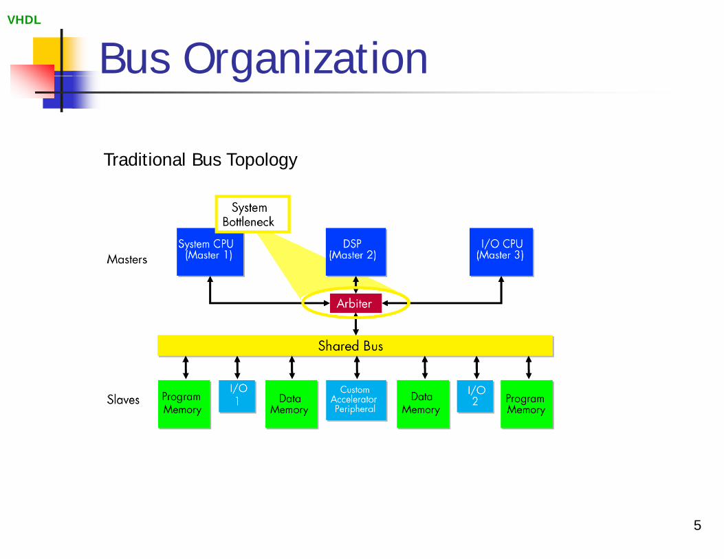
Bus Organizationg
Traditional Bus Topology
Digital Design — Chapter 7 — Processor Basics 5
VHDL
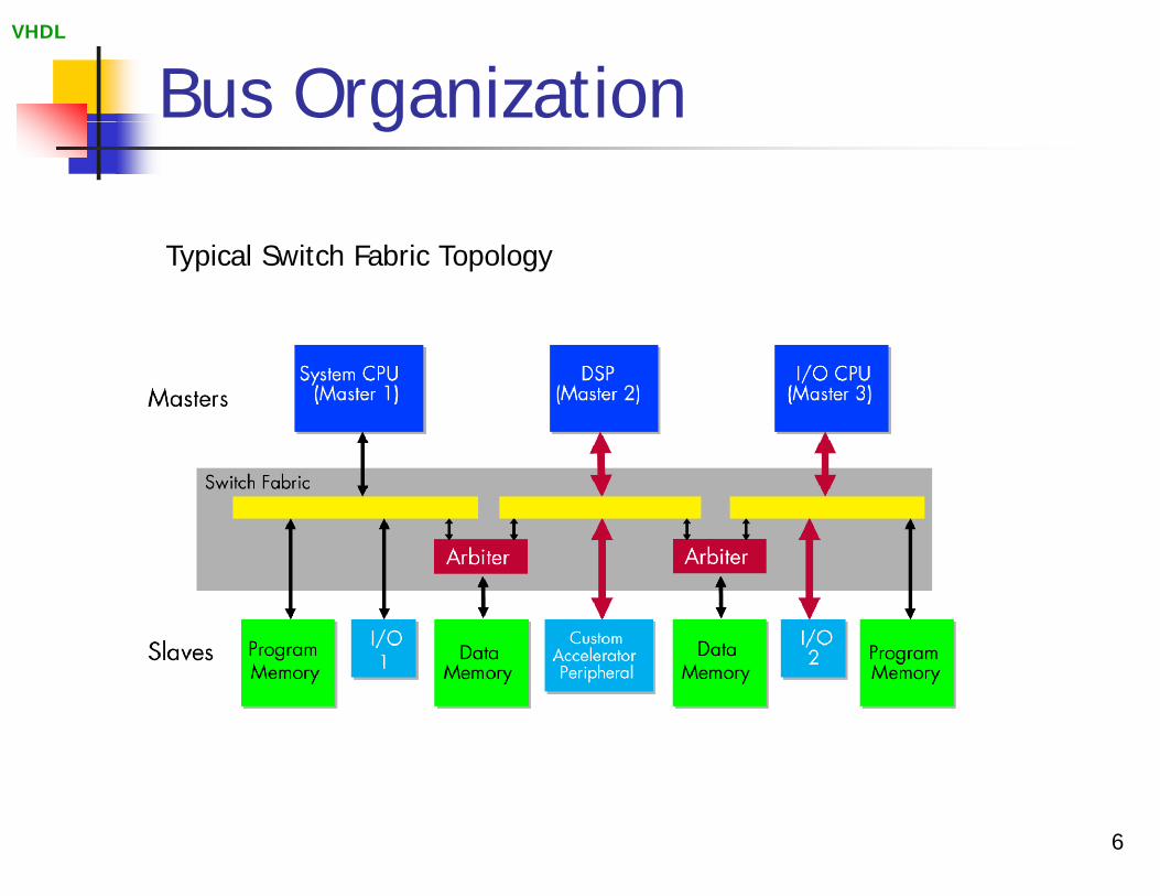
Bus Organizationg
Typical Switch Fabric Topology
Digital Design — Chapter 7 — Processor Basics 6

VHDL
Bus OrganizationgAltera’s System Interconnect Fabric Example
Digital Design — Chapter 7 — Processor Basics 7

VHDL
Bus OrganizationgAltera’s Memory-Mapped and Streaming System Interconnect Fabrics
SRIO:Serial RapidIO is a high-performance, point-to-point, packet-switched interconnect technology defined by the RapidIO Trade Association.
Full-duplex point-to-pointFull duplex point to point links are established with single or multiple high-speed serial lanes (1x and 4x are currently defined), and industry standardand industry-standard 8B/10B-encoded data transmission at signaling rates of 1.25, 2.50, or 3.125 Gbaud for peak bandwidth of up to 20 Gbps.
Digital Design — Chapter 7 — Processor Basics 8

VHDL
Microprocessorsp
Single-chip processor in a packageSingle chip processor in a packageExternal connections to memory and I/O bI/O busesMost commonly seen in generalMost commonly seen in general purpose computers
E g Intel Pentium family PowerPCE.g., Intel Pentium family, PowerPC, …
Digital Design — Chapter 7 — Processor Basics 9
VHDL
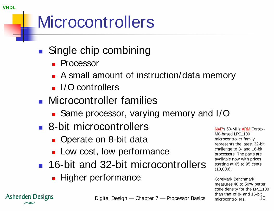
Microcontrollers
Single chip combiningg p gProcessorA small amount of instruction/data memoryyI/O controllers
Microcontroller familiesSame processor, varying memory and I/O
8-bit microcontrollers NXP’s 50-MHz ARM Cortex-
Operate on 8-bit dataLow cost, low performance
M0-based LPC1100 microcontroller family represents the latest 32-bit challenge to 8- and 16-bit processors. The parts are
16-bit and 32-bit microcontrollersHigher performance
available now with prices starting at 65 to 95 cents (10,000).
CoreMark Benchmark 0 0% b
Digital Design — Chapter 7 — Processor Basics 10
measures 40 to 50% better code density for the LPC1100 than that of 8- and 16-bit microcontrollers.

VHDL
Processor Cores
Processor as a component in an FPGA orProcessor as a component in an FPGA or ASICIn FPGA can be a fixed-function blockIn FPGA, can be a fixed-function block
E.g., PowerPC cores in some Xilinx FPGAs
O b ftOr can be a soft coreImplemented using programmable resourcesE.g., Xilinx MicroBlaze, Altera Nios-II
In ASIC, provided as an IP blockE.g., ARM, PowerPC, MIPS, Tensilica coresCan be customized for an application
Digital Design — Chapter 7 — Processor Basics 11

VHDL
Digital Signal Processors g g
DSPs are processors optimized forDSPs are processors optimized for signal processing operations
E di id d t i lE.g., audio, video, sensor data; wireless communication
Often combined with a conventional core for processing other datacore for processing other data
Heterogeneous multiprocessor
Digital Design — Chapter 7 — Processor Basics 12
VHDL
Instruction Sets
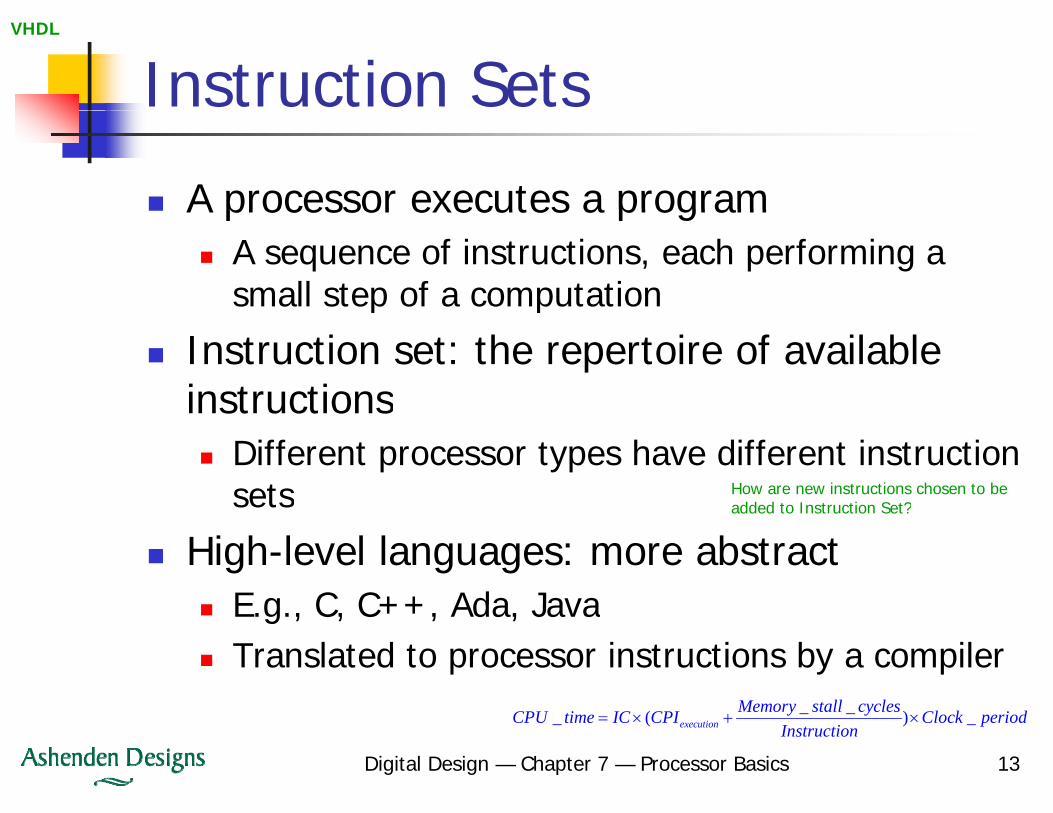
A processor executes a programA processor executes a programA sequence of instructions, each performing a small step of a computationp p
Instruction set: the repertoire of available instructionsinstructions
Different processor types have different instruction sets How are new instructions chosen to be
added to Instruction Set?sets
High-level languages: more abstractE g C C++ Ada Java
added to Instruction Set?
E.g., C, C++, Ada, JavaTranslated to processor instructions by a compiler
M t ll l
Digital Design — Chapter 7 — Processor Basics 13
_ __ ( ) _executionMemory stall cyclesCPU time IC CPI Clock period
Instruction= × + ×

VHDL
Instruction Execution
Instructions are encoded in binaryInstructions are encoded in binaryStored in the instruction memory
A processor executes a program byA processor executes a program by repeatedly
F t hi th t i t tiFetching the next instructionDecoding it to work out what to doExecuting the operation
Program counter (PC)g ( )Register in the processor holding the address of the next instruction
Digital Design — Chapter 7 — Processor Basics 14
add ess o t e e t st uct o

VHDL
Data and Endian-nessInstructions operate on data from the data memoryp yByte: 8-bit data
Data memory is usually byte addressed6 bi 32 bi 6 bi d f d16-bit, 32-bit, 64-bit words of data
Little endian Big endian
0
least sig. byte
8-bit data
m
0 8-bit data
most sig bytemg y16-bit data
most sig. byte
l i b
m + 1 least sig. byte16-bit data
most sig. bytem
m + 1
Little endianLSB=lowest address
Big endianMSB=lowest address
32-bit data
least sig. byte
most sig byte
n
n + 2
n + 3
n + 132-bit data
l i b
most sig. byten
n + 2
3
n + 1Intel x86 PowerPC
Digital Design — Chapter 7 — Processor Basics 15
most sig. byten + 3 least sig. byten + 3
VHDL
The Gumnut Core
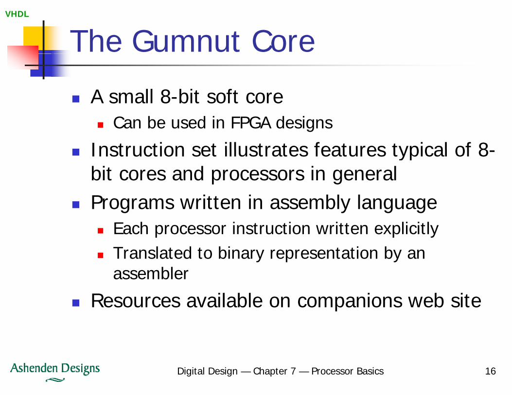
A small 8-bit soft coreA small 8 bit soft coreCan be used in FPGA designs
Instruction set illustrates features typical of 8-Instruction set illustrates features typical of 8-bit cores and processors in generalP itt i bl lPrograms written in assembly language
Each processor instruction written explicitlyTranslated to binary representation by an assembler
R il bl i b itResources available on companions web site
Digital Design — Chapter 7 — Processor Basics 16

VHDL
Gumnut StoragegGeneral-Purpose Registers Condition Code Registers
r0 0r1r2r3
CZ
P C
CarryZero
How many registers should you encode for in the instruction? Two? Three?
r4r5r6r7
PC
Program CounterTwo? Three?
How many registers should there be?
Data Memory(256 × 8-bit, 8-bit addresses)
Instruction Memory(4K × 18-bit, 12-bit addresses)
012
012
254255
40944095
Digital Design — Chapter 7 — Processor Basics 17
255 4095

VHDL
Arithmetic Instructions
Operate on register data and put resultOperate on register data and put result in a registeradd addc sub subcadd, addc, sub, subcCan have immediate value operand
C diti dCondition codesZ: 1 if result is zero, 0 if result is non-zeroC: carry out of add/addc, borrow out of sub/subc
addc and subc include C bit in operation
Digital Design — Chapter 7 — Processor Basics 18
p
VHDL
Arithmetic Instructions
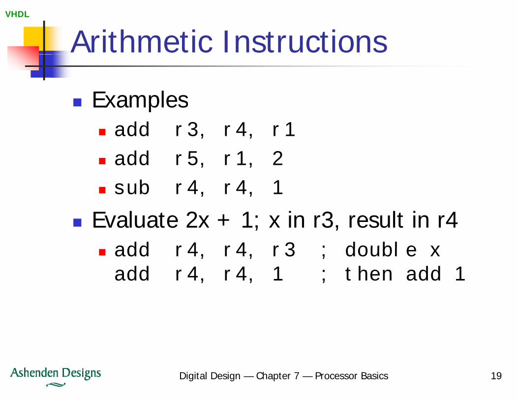
ExamplesExamplesadd r3, r4, r1
dd 5 1 2add r5, r1, 2
sub r4, r4, 1
Evaluate 2x + 1; x in r3, result in r4add r4 r4 r3 ; double xadd r4, r4, r3 ; double xadd r4, r4, 1 ; then add 1
Digital Design — Chapter 7 — Processor Basics 19

VHDL
Logical Instructionsg
Operate on register data and put resultOperate on register data and put result in a register
d k ( d t)and, or, xor, mask (and not)Operate bitwise on 8-bit operandsCan have immediate value operand
Condition codesCondition codesZ: 1 if result is zero, 0 if result is non-zeroC: always 0
Digital Design — Chapter 7 — Processor Basics 20

VHDL
Logical Instructionsg
Examplespand r3, r4, r5
or r1, r1, 0x80 ; set r1(7)
xor r5, r5, 0xFF ; invert r5
Set Z if least-significant 4 bits of r2 are 0101gand r1, r2, 0x0F ; clear high bitssub r0, r1, 0x05 ; compare with 0101
Digital Design — Chapter 7 — Processor Basics 21

VHDL
Shift Instructions
Logical shift/rotate register data andLogical shift/rotate register data and put result in a register
hl h lshl, shr, rol, rorCount specified as a literal operand
Condition codesZ: 1 if result is zero 0 if result is non-zeroZ: 1 if result is zero, 0 if result is non-zeroC: the value of the last bit shifted/rotated
t th d f th b tpast the end of the byte
Digital Design — Chapter 7 — Processor Basics 22
VHDL
Shift Instructions
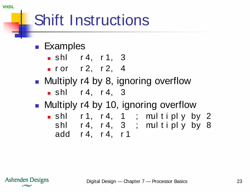
Examplespshl r4, r1, 3
ror r2, r2, 4
Multiply r4 by 8, ignoring overflowshl r4, r4, 3
Multiply r4 by 10, ignoring overflowshl r1, r4, 1 ; multiply by 2, , ; p y yshl r4, r4, 3 ; multiply by 8add r4, r4, r1
Digital Design — Chapter 7 — Processor Basics 23

VHDL
Memory Instructionsy
Transfer data between registers and data gmemory
Compute address by adding an offset to a base register value
Load register from memoryldm r1, (r2)+5
Store from register to memorystm r1, (r4)-2
Use r0 if base address is 0ldm r3, 23 ≡ ldm r3, (r0)+23
Condition codes not affected
Digital Design — Chapter 7 — Processor Basics 24
VHDL
Memory Instructionsy
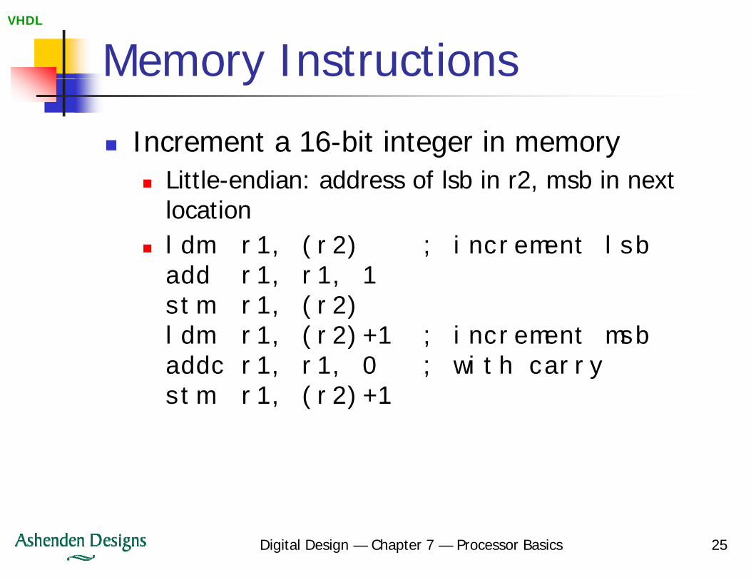
Increment a 16-bit integer in memoryIncrement a 16 bit integer in memoryLittle-endian: address of lsb in r2, msb in next locationldm r1, (r2) ; increment lsbadd r1, r1, 1stm r1, (r2)ldm r1, (r2)+1 ; increment msbaddc r1 r1 0 ; with carryaddc r1, r1, 0 ; with carrystm r1, (r2)+1
Digital Design — Chapter 7 — Processor Basics 25

VHDL
Input/Output Instructionsp / p
I/O controllers have registers that governI/O controllers have registers that govern their operation
Each has an address like data memoryEach has an address, like data memoryGumnut has separate data and I/O address spaces
Input from I/O registerInput from I/O registerinp r3, 157 ≡ inp r3, (r0)+157
O t t t I/O i tOutput to I/O registerout r3, (r7) ≡ out r3, (r7)+0
Condition codes not affectedFurther examples in Chapter 8
Digital Design — Chapter 7 — Processor Basics 26
p p

VHDL
Branch Instructions
Programs can evaluate conditions and takePrograms can evaluate conditions and take alternate courses of action
Condition codes (Z C) represent outcomes ofCondition codes (Z, C) represent outcomes of arithmetic/logical/shift instructions
Branch instructions examine Z or CBranch instructions examine Z or Cbz, bnz, bc, bncAdd a displacement to PC if condition is trueAdd a displacement to PC if condition is trueSpecifies how many instructions forward or backward to skipbackward to skip
Counting from instruction after branch
Digital Design — Chapter 7 — Processor Basics 27

VHDL
Branch Examplep
Elapsed seconds in location 100Elapsed seconds in location 100Increment, wrapping to 0 after 59ldm r1, 100ldm r1, 100add r1, r1, 1sub r0, r1, 60 ; Z set if r1 = 60bnz +1 ; Skip to store ifadd r1, r0, 0 ; Z is 0stm r1 100stm r1, 100
Digital Design — Chapter 7 — Processor Basics 28
VHDL
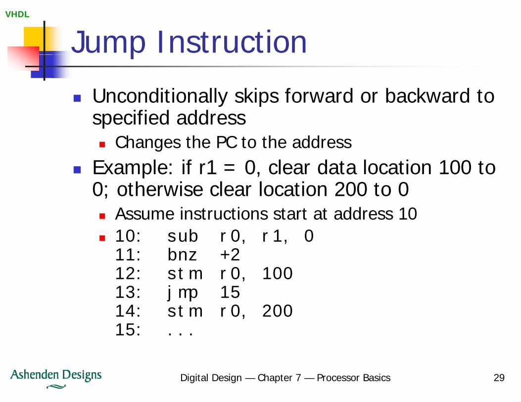
Jump Instructionp
Unconditionally skips forward or backward to y pspecified address
Changes the PC to the addressExample: if r1 = 0, clear data location 100 to 0; otherwise clear location 200 to 0
Assume instructions start at address 1010: sub r0, r1, 011 b 211: bnz +212: stm r0, 10013: jmp 15j p14: stm r0, 20015: ...
Digital Design — Chapter 7 — Processor Basics 29
VHDL
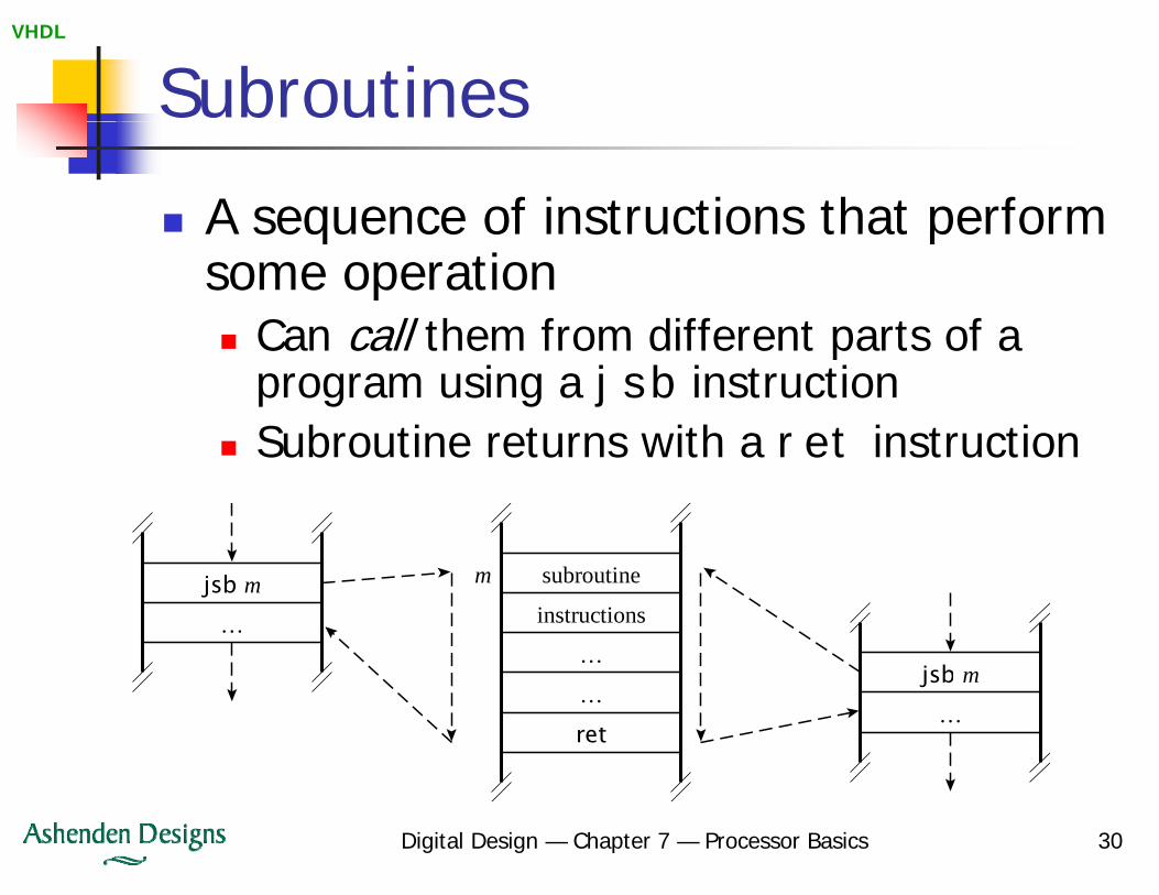
Subroutines
A sequence of instructions that performA sequence of instructions that perform some operation
Can call them from different parts of aCan call them from different parts of a program using a jsb instructionSubroutine returns with a ret instructionSubroutine returns with a ret instruction
subroutine
instructions
……
mjsb m
b…
ret…
jsb m
Digital Design — Chapter 7 — Processor Basics 30

VHDL
Subroutine ExamplepSubroutine to increment second count
Address of count in r2ldm r1, (r2)add r1 r1 1add r1, r1, 1sub r0, r1, 60bnz +1add r1 r0 0add r1, r0, 0stm r1, (r2)ret
Call to increment locations 100 and 102add r2, r0, 100jsb 20jsb 20add r2, r0, 102jsb 20
Digital Design — Chapter 7 — Processor Basics 31

VHDL
Return Address Stack
The jsb saves the return address forThe jsb saves the return address for use by the ret
B t h t if th b ti i l d j b?But what if the subroutine includes a jsb?
Gumnut core includes an 8-entry push-y pdown stack of return addresses
return addr for third call
return addr for first call
return addr for second call
return addr for first call
return addr for second call
Digital Design — Chapter 7 — Processor Basics 32
VHDL
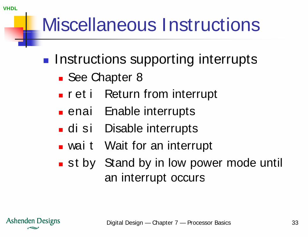
Miscellaneous Instructions
Instructions supporting interruptsInstructions supporting interruptsSee Chapter 8
i R t f i t treti Return from interruptenai Enable interruptsdisi Disable interruptswait Wait for an interruptwait Wait for an interruptstby Stand by in low power mode until
an interrupt occursan interrupt occurs
Digital Design — Chapter 7 — Processor Basics 33

VHDL
The Gumnut Assembler
Gasm: translates assembly programsGasm: translates assembly programsGenerates memory images for program text (binary coded instructions) and datatext (binary-coded instructions) and dataSee documentation on web site
Write a program as a text fileInstructionsInstructionsDirectivesC tCommentsUse symbolic labels
Digital Design — Chapter 7 — Processor Basics 34
VHDL
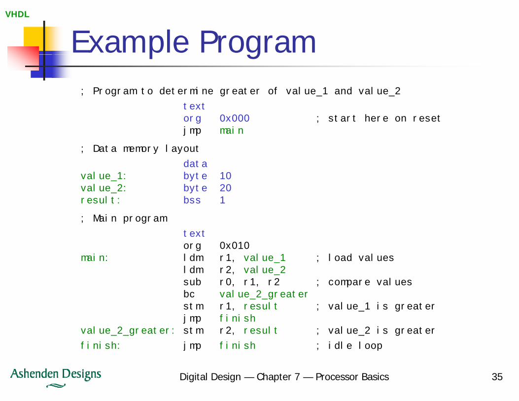
Example Programp g; Program to determine greater of value_1 and value_2
t ttextorg 0x000 ; start here on resetjmp main
; Data memory layout; t e o y yout
datavalue_1: byte 10value_2: byte 20result: bss 1result: bss 1
; Main program
textorg 0x010g
main: ldm r1, value_1 ; load valuesldm r2, value_2sub r0, r1, r2 ; compare valuesbc value_2_greater_ _gstm r1, result ; value_1 is greaterjmp finish
value_2_greater: stm r2, result ; value_2 is greater
finish: jmp finish ; idle loop
Digital Design — Chapter 7 — Processor Basics 35
finish: jmp finish ; idle loop

VHDL
Gumnut Instruction Encodingg
Instructions are a form of informationInstructions are a form of informationCan be encoded in binary
Gumnut encoding18 bits per instructionpDivided into fields representing different aspects of the instructionaspects of the instruction
Opcodes and function codesRegister numbers The VAX has a computer architecture with easilyRegister numbersAddresses
The VAX has a computer architecture with easily the most complex instruction set.
The instruction set has a highly variable format where the minimal instruction length is 1 byte
d h l b ( b )
Digital Design — Chapter 7 — Processor Basics 36
and the longest instruction is 37 bytes (296 bits).

VHDL
Gumnut Instruction EncodinggArith/Logical
1 1 01 fd 24 3 33 3 2
gRegister
Arith/LogicalImmediate
1 1 01 fnrd rs rs2
0 fn rd rs immed1 83 3 3
Immediate
Shift 1 1 0 fnrd rs count3 31 23 3 3
6 2 2 8
Memory, I/O 1 0 fn rd rs offset2 2 3 3 8
1 1 01 1 1 fn dispBranch
1 1 1 1 0 fn addr5 1 12
Jump 1 1 1 1 0
0
fn addrJump
1 1 1 1 1 1 fn7 3 8
Miscellaneous
Digital Design — Chapter 7 — Processor Basics 37

VHDL
Encoding Examplesg p
Encoding for addc r3 r5 24Encoding for addc r3, r5, 24Arithmetic immediate, fn = 001
0 fn rd rs immed
0 00 1 10 1 01 1 0 0 10 1 00 0
1 83 3 3
05D18
Instruction encoded by 2ECFCInstruction encoded by 2ECFC1 1 0 0 01 1 1 1 1 1 1 11 1 0 01
1 1 01 1 1 fn disp6 2 2 8
Branch bnc -4
Digital Design — Chapter 7 — Processor Basics 38

VHDL
Other Instruction Sets
8-bit cores and microcontrollers8 bit cores and microcontrollersXilinx PicoBlaze: like Gumnut8051 and numerous like it8051, and numerous like it
Originated as 8-bit microprocessorsInstructions encoded as one or more bytesInstruction set is more complex and irregularComplex instruction set computer (CISC)C f R d d i i (RISC)C.f. Reduced instruction set computer (RISC)
16-, 32- and 64-bit coresMostly RISCE.g., PowerPC, ARM, MIPS, Tensilica, …
Digital Design — Chapter 7 — Processor Basics 39

VHDL
Instruction and Data Memoryy
In embedded systemsIn embedded systemsInstruction memory is usually ROM, flash, SRAM or combinationSRAM, or combinationData memory is usually SRAM
DRAM if large capacity needed
Processor/memory interfacing/ y gGluing the signals together
Digital Design — Chapter 7 — Processor Basics 40

VHDL
Example: Gumnut Memoryp y
gumnut dataSRAM
instructionROM
rst_iSRAM
inst_cyc_oinst stb o
data_cyc_odata stb o
enen
clk_iclk_i
ROMclk_i
inst_stb_o
inst_ack_i
data_stb_o
data_ack_i
data we o we
D Q
clk
DQ
clk
inst_adr_oinst_dat_i data_adr_o
data_dat_idata_dat_o
data_we_o
adr
dat_odat_i
weadr
dat_o
Digital Design — Chapter 7 — Processor Basics 41

VHDL
Example: Gumnut Memoryp y
IMem : process (clk) isbegin
if rising edge(clk) thenif rising_edge(clk) thenif inst_cyc_o = '1' and inst_stb_o = '1' then
inst_dat_i <=instr_ROM(to_integer(inst_adr_o(10 downto 0)));( g ( ( )));
inst_ack_i <= '1';else
inst_ack_i <= '0';end if;
end if;end process IMem;
Digital Design — Chapter 7 — Processor Basics 42

VHDL
Example: Gumnut Memoryp y
DMem : process (clk) isDMem : process (clk) isbegin
if rising_edge(clk) thenif data_cyc_o = '1' and data_stb_o = '1' thendata_cyc_o a d data_stb_o t e
if data_we_o = '1' thendata_RAM(to_integer(data_adr_o)) <= data_dat_o;data_dat_i <= data_dat_o;;data_ack_i <= '1';
elsedata_dat_i <= data_RAM(to_integer(data_adr_o));data_ack_i <= '1';
end if;else
d k i ' 'data_ack_i <= '0';end if;
end if;d DM
Digital Design — Chapter 7 — Processor Basics 43
end process DMem;

VHDL
Example: Microcontroller Memoryp y
A(15..8)
D
P2
8051 SRAM
A(7..0)D
LE
Q
ALE
P0
WE
A(16)PSEN
WR
CE
OERD
PSEN (program store enable)
Digital Design — Chapter 7 — Processor Basics 44

VHDL
32-bit Memoryy
Four bytes per memory wordFour bytes per memory wordLittle-endian: lsb at least addressBig-endian: msb at least addressBig endian: msb at least address
0 1 2 34 5 6 74 5 6 78 9 10 11
Partial-word readRead all bytes, processor selects those neededRead all bytes, processor selects those needed
Partial-word writeUse byte-enable signals
Digital Design — Chapter 7 — Processor Basics 45
Use byte-enable signals

VHDL
Example: MicroBlaze Memoryp ySSRAM2:16
Addr
D_in
A
en
wr
D_out
clk
0:70:7
dd
Data_Write
AS
Write_Strobe
Byte_Enable(0)
Byte Enable(1)
D_in
A
SSRAM
en
D_out8:158:15Read_Strobe
Data Read
Byte_Enable(1)
Byte_Enable(2)
Byte_Enable(3)
wr
clk
A
SSRAM
16:2316:23
Ready
Clk
Data_Read
+V
D_in
en
wr
D_out
clk
SSRAM
D_in
A
SSRAM
en
wr
D_out
lk
24:3124:31
Digital Design — Chapter 7 — Processor Basics 46
clk
VHDL
Cache Memoryy
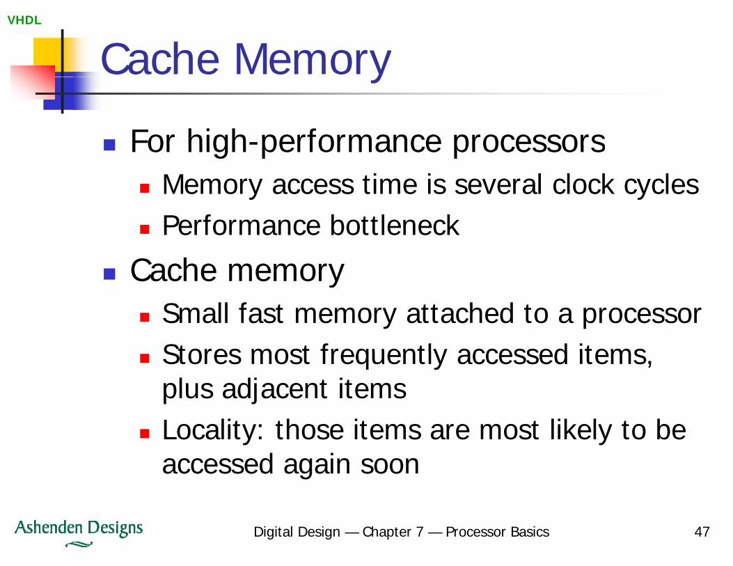
For high-performance processorsFor high performance processorsMemory access time is several clock cyclesP f b l kPerformance bottleneck
Cache memoryySmall fast memory attached to a processorStores most frequently accessed itemsStores most frequently accessed items, plus adjacent itemsL lit th it t lik l t bLocality: those items are most likely to be accessed again soon
Digital Design — Chapter 7 — Processor Basics 47
VHDL
Cache Memoryy
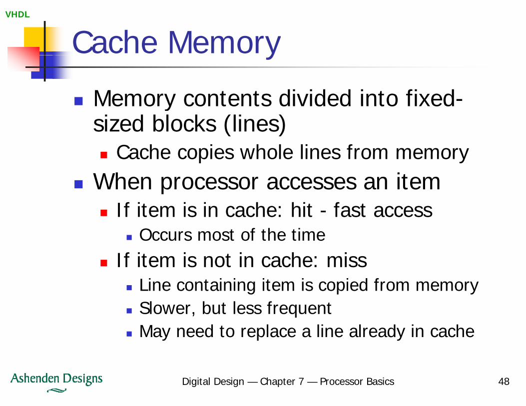
Memory contents divided into fixed-Memory contents divided into fixedsized blocks (lines)
Cache copies whole lines from memoryCache copies whole lines from memoryWhen processor accesses an item
If it i i h hit f tIf item is in cache: hit - fast accessOccurs most of the time
If i i i h iIf item is not in cache: missLine containing item is copied from memorySl b t l f tSlower, but less frequentMay need to replace a line already in cache
Digital Design — Chapter 7 — Processor Basics 48

VHDL
Fast Main Memory Accessy
Optimize memory for line access by cacheOptimize memory for line access by cacheWide memory
Read a line in one access
Burst transfersSend starting address, then read successive locations
PipeliningOverlapping stages of memory accessE.g., address transfer, memory operation, data transfer
Double data rate (DDR), Quad data rate (QDR)Transfer on both rising and falling clock edges
Digital Design — Chapter 7 — Processor Basics 49

VHDL
Summaryy
Embedded computerEmbedded computerProcessor, memory, I/O controllers, buses
Microprocessors microcontrollers andMicroprocessors, microcontrollers, and processor coresS f f S C/ GSoft-core processors for ASIC/FPGAProcessor instruction sets
Binary encoding for instructionsAssembly language programsAssembly language programsMemory interfacing
Digital Design — Chapter 7 — Processor Basics 50