Chapter 01
33
The PIC18 Microcontroller Chapter 1: Introduction to PIC18 The PIC18 Microcontroller Han-Way Huang Minnesota State University Mankato Minnesota State University , Mankato H. Huang Transparency No.1-1 Copyright @ 2005 Thomson Delmar Learning
description
Credit to the writer
Transcript of Chapter 01

The PIC18 Microcontroller
Chapter 1: Introduction to PIC18
The PIC18 Microcontroller
Han-Way Huang
Minnesota State University MankatoMinnesota State University, Mankato
H. Huang Transparency No.1-1Copyright @ 2005 Thomson Delmar Learning

The PIC18 Microcontroller
What is a computer?
Software
HardwareHardware
Computer Hardware OrganizationP ro c e sso r
Co ntro l U nit
C o m m o n B us (addre ss , data, & c o ntro l)
D atapath
Arithm e ticLo gic U nit M e m o ry
R e gis te rsP ro gramSto rage
D ataSto rage
O utputU nits
InputU nits
H. Huang Transparency No.1-2Copyright @ 2005 Thomson Delmar Learning
Figure 1 .1 C o m pute r O rganizatio n

The PIC18 Microcontroller
ThThe processorRegisters -- storage locations in the processor
Arithmetic logic unitArithmetic logic unit
Control unit
program counter contains the address of the next instruction to be executedp g
status register flags the instruction execution result
The microprocessorA processor implemented on a very large scale integration (VLSI) chip
Peripheral chips are needed to construct a product
The MicrocontrollerThe processor and peripheral functions implemented on one VLSI chip
H. Huang Transparency No.1-3Copyright @ 2005 Thomson Delmar Learning

The PIC18 Microcontroller
Features of the PIC18 microcontrollerFeatures of the PIC18 microcontroller- 8-bit CPU- 2 MB program memory space- 256 bytes to 1KB of data EEPROM- Up to 3968 bytes of on-chip SRAM- 4 KB to 128KB flash program memory- Sophisticated timer functions that include: input capture, output compare,
PWM, real-time interrupt, and watchdog timer- Serial communication interfaces: SCI SPI I2C and CANSerial communication interfaces: SCI, SPI, I2C, and CAN- Background debug mode (BDM)- 10-bit A/D converter
M t ti bilit- Memory protection capability- Instruction pipelining- Operates at up to 40 MHz crystal oscillator
H. Huang Transparency No.1-4Copyright @ 2005 Thomson Delmar Learning

The PIC18 Microcontroller
Embedded SystemsEmbedded Systems
- A product that uses one or more microcontrollers as controller (s).
- End users are only interested in the functionality of the product but not on the microcontroller itself.
- Cell phones, home security system, automobiles, and many other products are examples of embedded products.
H. Huang Transparency No.1-5Copyright @ 2005 Thomson Delmar Learning

The PIC18 Microcontroller
Semiconductor memoryy
• Random-access memory (RAM): same amount of time is required to access any location on the same chipR d l (ROM) l b d b t t itt t b th• Read-only memory (ROM): can only be read but not written to by the processor
Random-access memory
• Dynamic random-access memory (DRAM): need periodic refresh• Static random-access memory (SRAM): no periodic refresh is required
Read-only memory
• Mask-programmed read-only memory (MROM): programmed when beingMask programmed read only memory (MROM): programmed when being manufactured
• Programmable read-only memory (PROM): can be programmed by the end user
H. Huang Transparency No.1-6Copyright @ 2005 Thomson Delmar Learning

The PIC18 Microcontroller
Erasable programmable ROM (EPROM)Erasable programmable ROM (EPROM)
1. electrically programmable many times2. erased by ultraviolet light (through a window)3 bl i b lk ( h l hi i ti )3. erasable in bulk (whole chip in one erasure operation)
Electrically erasable programmable ROM (EEPROM)
1. electrically programmable many times2. electrically erasable many times3. can be erased one location, one row, or whole chip in one operation
Flash memory
1. electrically programmable many times2. electrically erasable many times3. can only be erased in bulk (either a block or the whole chip)
H. Huang Transparency No.1-7Copyright @ 2005 Thomson Delmar Learning

The PIC18 Microcontroller
Computer software
- Computer programs are known as software- A program is a sequence of instructions
Machine instruction
- A sequence of binary digits which can be executed by the processord d d d d b f h b i- Hard to understand, program, and debug for human being
Assembly language
- Defined by assembly instructions- An assembly instruction is a mnemonic representation of a machine
instructionA bl t b t l t d b f it b t d- Assembly programs must be translated before it can be executed --translated by an assembler
- Programmers need to work on the program logic at a very low level and can’t achieve high productivity.
H. Huang Transparency No.1-8Copyright @ 2005 Thomson Delmar Learning
g p y

The PIC18 Microcontroller
High-level languageHigh-level language
- Syntax of a high-level language is similar to English- A translator is required to translate the program written in a
high-level language -- done by a compiler- Allows the user to work on the program logic at higher level.
Source codeSource code
- A program written in assembly or high-level language
Object code
- The output of an assembler or compiler
H. Huang Transparency No.1-9Copyright @ 2005 Thomson Delmar Learning

The PIC18 Microcontroller
Source code and object code examples
address object code line no. Source codej----------------------------------------------------------------------------------------------
00001E 0E06 00010 movlw 0x06000020 6E11 00011 movwf 0x11,A,000022 0E07 00012 movlw 0x07000024 6E12 00013 movwf 0x12,A000026 0E08 00014 movlw 0x080000 6 0 08 000 ov w 0 08000028 6E13 00015 movwf 0x13,A00002A 0E05 00016 movlw 0x0500002C 5E10 00017 subwf 0x10,F,A00002C 5E10 00017 subwf 0x10,F,A00002E 5E11 00018 subwf x11,F,A
H. Huang Transparency No.1-10Copyright @ 2005 Thomson Delmar Learning

The PIC18 Microcontroller
Radix Specificationp
- Hexadecimal (or hex) number is specified by adding the prefix 0x or by enclosing the number with single quotes and preceding it by an H.
0x02 0x1234 H`2040’ are hex numbers- 0x02, 0x1234, H 2040’ are hex numbers
- Decimal numbers are enclosed by single quotes and preceded by letter D.
- D`10’ and D`123’ are decimal numbers
- Octal and binary numbers are similarly specified.
- O`234’ is an octal number; B’01011100’ is a binary number.
H. Huang Transparency No.1-11Copyright @ 2005 Thomson Delmar Learning

The PIC18 Microcontroller
Memory Addressing
- Memory consists of a sequence of directly addressable locations.A l i i f d i f i i- A location is referred to as an information unit.
- A memory location can be used to store data, instruction, and the status of peripheral devices.
- A memory location has two components: an address and its contents.y p
Address Contents
Figure 1.2 The components of a memory location
H. Huang Transparency No.1-12Copyright @ 2005 Thomson Delmar Learning

The PIC18 Microcontroller
The PIC18 Memory Organization
- Data Memory and Program Memory are separatedData Memory and Program Memory are separated
- Separation of data memory and program memory makes possible the simultaneous access of data and instruction.
- Data memory are used as general-purpose registers or special function registers
- On-chip Data EEPROM are provided in some PIC18 MCUsp p
H. Huang Transparency No.1-13Copyright @ 2005 Thomson Delmar Learning

The PIC18 Microcontroller
Separation of Data Memory and Program Memory
Inside the c chip
ProgramMemory
Space
DataMemory
21-bit progam address 12-bit register address
Space(a portion
of thisspace is on
th
PIC18CPU
Space(Specialfunction
registers andlthe c
chip)generalpurposeRAM)
16-bit instruction bus 8-bit data bus
Figure 1.3 The PIC18 memory spaces
H. Huang Transparency No.1-14Copyright @ 2005 Thomson Delmar Learning

The PIC18 Microcontroller
PIC18 Data Memory
- Implemented in SRAM and consists of general-purpose registers and special-function registers. Both are referred to as data registers.
- A PIC18 MCU may have up to 4096 bytes of data memory.C 8 CU ay ave up to 096 bytes o data e o y.
- Data memory is divided into banks. Each bank has 256 bytes.
- General-purpose registers are used to hold dynamic data.
- Special-function registers are used to control the operation of peripheral functions.
- Only one bank is active at any time. The active bank is specified by the BSRregisterregister.
- Bank switching is an overhead and can be error-prone
- PIC18 implements the access bank to reduce the problem caused by bank switching.
- Access bank consists of the lowest 96 bytes and the highest 160 bytes of the data memory space.
H. Huang Transparency No.1-15Copyright @ 2005 Thomson Delmar Learning

The PIC18 Microcontroller
Access RAM 000h05Fh
BSR<3:0>
= 0000GPRs
05Fh060h
0FFh100h
1FFh
GPRs
Bank 0
Bank 1
0000
= 0001
200h
2FFh300h
GPRs
GPRs A RAM l 000hAccess Bank
Bank 2
Bank 3
= 0010
= 0011
3FFh400h
GPRs
Access RAM low
Access RAM highSFRs
000h05Fh060h
0FFhBank 4
toB k 13
GPRs
DFFhE00h
EFFh
Bank 13
Bank 14= 1110
Note. 1. BSR is the 4-bit bank select register.
Unused
SFRs
EFFhF00hF5FhF60h
FFFh
Bank 15= 1111
H. Huang Transparency No.1-16Copyright @ 2005 Thomson Delmar Learning
Figure 1.4 Data memory map for PIC18 devices (redraw with permission of Microchip)

The PIC18 Microcontroller
Program Memory OrganizationProgram Memory Organization
- The program counter (PC) is 21-bit long, which enables the user program to access up to 2 MB of program memory.
- The PIC18 has a 31-entry return address stack to hold the return address for subroutine call.
- After power-on, the PIC18 starts to execute instructions from address 0.
- The location at address 0x08 is reserved for high-priority interrupt service routine.
- The location at address 0x18 is reserved for low-priority interrupt serviceThe location at address 0x18 is reserved for low priority interrupt service routine.
- Up to 128KB (at present time) of program memory is inside the MCU chip.
P t f th i l t d t id f th MCU hi- Part of the program memory is located outside of the MCU chip.
H. Huang Transparency No.1-17Copyright @ 2005 Thomson Delmar Learning

The PIC18 MicrocontrollerP C < 2 0 :0 >
2 1
s ta c k le v e l 1
s ta c k le v e l 3 1
.
.
.s ta c k le v e l 3 1
0 0 0 0 0 0h
0 0 0 0 0 8 h
R e s e t V e c to r
H igh P r io r ity In te r ru p t V e c to r
0 0 0 0 1 8 hL o w P r io r ity In te r ru p t V e c to r
y Sp
ace
O n -c h ip a n d e xte rn a l
y xxxxxh Use
r Mem
oryp r o gra m m e m o r y
1 F F F F F h
U n im p le m e n te dp ro gra m m e m o r y
R e a d ' 0 '
H. Huang Transparency No.1-18Copyright @ 2005 Thomson Delmar Learning
1 F F F F F h
F igu re 1 . 5 P IC 1 8 P ro gra m m e m o ry O rga n iz a t io n ( r e d ra w w ith p e rm is s io n o fM ic ro c h ip )
N o t e . y c a n b e 0 o r 1 w h e r e a s x c a n b e 0 -F

The PIC18 Microcontroller
The PIC18 CPU RegisterThe PIC18 CPU Register
- The group of registers from 0xFD8 to 0xFFF are dedicated to the general control of MCU operation.
h i li d i bl- The CPU registers are listed in Table 1.2.
- The WREG register is involved in the execution of many instructions.
- The STATUS register holds the status flags for the instruction execution and isThe STATUS register holds the status flags for the instruction execution and is shown in Figure 1.6.
H. Huang Transparency No.1-19Copyright @ 2005 Thomson Delmar Learning

The PIC18 Microcontroller
n er la
tch
latc
hby
teyt
e e ter
ter 2
ter 3
oint
er 0
0 (t
o G
PRs)
r 0 (t
o G
PRs)
0 (to
GPR
s)
gh b
yte
w b
yte
oint
er 1
1 (t
o G
PRs)
r 1 (t
o G
PRs)
1 (to
GPR
s)
gh b
yte
w b
yte
oint
er 2
2 (t
o G
PRs)
r 2 (t
o G
PRs)
2 (to
GPR
s)
gh b
yte
w b
yte
Des
crip
tion
ack
(upp
er)
ack
(hig
h)ac
k (lo
w)
nter
rogr
am c
ount
egr
am c
ount
er c
ount
er lo
w b
inte
r upp
er b
yin
ter h
igh
byte
inte
r low
byt
ech du
ct re
gist
erdu
ct re
gist
er c
ontr
ol re
gis t
con
trol
regi
st c
ontr
ol re
gist
ile re
gist
er p
oem
ent p
oint
erem
ent p
oint
erm
ent p
oint
er 0
EG to
FSR
0t
regi
ster
0 h
it r
egis
ter 0
low
regi
ster
ile re
gist
er p
oem
ent p
oint
erem
ent p
oint
erm
ent p
oint
er 1
EG to
FSR
1t
regi
ster
1 h
it r
egis
ter 1
low
ect r
egis
ter
ile re
gist
er p
oem
ent p
oint
erem
ent p
oint
e rm
ent p
oint
er 2
EG to
FSR
2t
regi
ster
2 h
it r
egis
ter 2
low
gost
er
iste
rs
1) 1) ) 1) 1) ) 1) (1)
)
Top
of s
taTo
p of
sta
Top
of s
taSt
ack
poi
Upp
er p
rH
igh
pro
Prog
ram
Ta
ble
poi
Tabl
e po
iTa
ble
poi
Tabl
e la
tcH
igh
pro
Low
pro
dIn
terr
upt
Inte
rrup
tIn
terr
upt
Indi
rect
fPo
st in
cre
Post
dec
rPr
einc
rem
Add
WRE
File
sel
ect
File
sel
ect
Wor
king
In
dire
ct f
Post
incr
ePo
st d
ecr
Prei
ncre
mA
dd W
REFi
le s
elec
tFi
le s
elec
tBa
nk s
ele
Indi
rect
fPo
st in
cre
Post
dec
rPr
einc
rem
Add
WRE
File
sel
ect
File
sel
ect
Stat
us re
g
sica
l reg
iser
C18
CPU
reg
Nam
eTO
SUTO
SHTO
SLST
KPT
RPC
LATU
PCLA
THPC
LTB
LPTR
UTB
LPTR
HTB
LPTR
LTA
BLA
TPR
OD
HPR
OD
LIN
TCO
NIN
TCO
N2
INTC
ON
3IN
DF0
(1)
POST
INC
0 (1
POST
DEC
0 (
PREI
NC
0 (1
)
PLU
SW0
(1)
FSR0
HFS
R0L
WRE
GIN
DF1
(1)
POST
INC
1 (1
POST
DEC
1 (
PREI
NC
1 (1
)
PLU
SW1
(1)
FSR1
HFS
R1L
BSR
IND
F2 (1
)
POST
INC
2 (1
POSR
DEC
2 (
PREI
NC
2 (1
)
PLU
SW2
(1)
FSR2
HFS
R2L
STA
TUS
is n
ot a
phy
s
Tabl
e 1.
2 PI
Cad
dres
s0x
FFF
0xFF
E0x
FFD
0xFF
C0x
FFB
0xFF
A0x
FF9
0xFF
80x
FF7
0xFF
60x
FF5
0xFF
40x
FF3
0xFF
20x
FF1
0xFF
00x
FEF
0xFE
E0x
FED
0xFE
C0x
FEB
0xFE
A0x
FE9
0xFE
80x
FE7
0xFE
60x
FE5
0xFE
40x
FE3
0xFE
20x
FE1
0xFE
00x
FDF
0xFD
E0x
FDD
0xFD
C0x
FDB
0xFD
A0x
FD9
0xFD
8
Not
e 1.
Thi
s
H. Huang Transparency No.1-20Copyright @ 2005 Thomson Delmar Learning
T N

The PIC18 Microcontroller
ip)
C
. zero
.
. occu
rred
.oc
curr
ed.
LF)
3 of
the
. lt oc
curr
ed.
ult h
as
LF)
w o
rder
bit0
ssio
n of
Mic
roch
i
ZD
C
met
ic
oper
atio
n is
zer
oop
erat
ion
is n
ot z
BW
F in
stru
ctio
ns.
bit o
f the
resu
lt o
r bit
of th
e re
sult
r rot
ate
(RR
F, R
Ler
the
bit 4
or b
it
BW
F in
stru
ctio
ns.
nt b
it of
the
resu
lan
t bit
of th
e re
su
r rot
ate
(RR
F, R
Ler
the
high
or l
ow
21
draw
with
per
mis
NO
V
nega
tive
posi
tive
d fo
r sig
ned
arith
mrr
ed ithm
etic
or l
ogic
oith
met
ic o
r log
ic o
it W, S
UB
LW, S
UB
he 4
th lo
w-o
rder
th
e 4t
h lo
w-o
rde r
ty is
reve
rsed
. Fo
load
ed w
ith e
ithe
W, S
UB
LW, S
UB
he m
ost s
igni
fican
the
mos
t sig
nific
ty is
reve
rsed
. Fo
load
ed w
ith e
ithe
43
ster
(0xF
D8)
(re d
----
tive
bit
ithm
etic
resu
lt is
ith
met
ic re
sult
is
erflo
w b
itve
rflo
w o
ccur
red
o ov
erflo
w o
ccur
flag
he re
sult
of a
n ar
ihe
resu
lt of
an
ari
it ca
rry/
borr
ow b
iD
DW
F, A
DD
LWca
rry-
out f
rom
tho
carr
y-ou
t fro
m
orro
w, t
he p
olar
itct
ions
, thi
s bit
is
e re
gist
er.
/bor
row
bit
DD
WF,
AD
DLW
carr
y-ou
t fro
m th
o ca
rry-
out f
rom
cc
urre
d.or
row
, the
pol
arit
ctio
ns, t
his b
it is
so
urce
regi
ster
.
65
he S
TATU
S re
gi
--
N: N
egat
1
= a
ri
0 =
ari
OV
: Ove
1
= O
v
0 =
No
Z: Z
ero
f
1 =
Th
0
= T
hD
C: D
igi
F
or A
D
1 =
A
0
= N
o
For
bo
i
nstru
c
sou
rce
C: C
arry
/
For
AD
1
= A
0 =
No
o
c
For
bo
i
nstru
c
of t
he
7
Figu
re 1
.6 T
h
H. Huang Transparency No.1-21Copyright @ 2005 Thomson Delmar Learning
The PIC18 Microcontroller
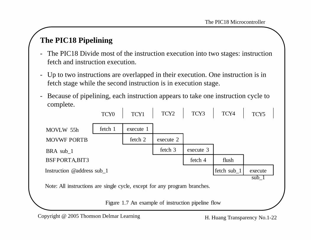
The PIC18 Pipeliningp g
- The PIC18 Divide most of the instruction execution into two stages: instruction fetch and instruction execution.
Up to two instructions are overlapped in their execution One instruction is in- Up to two instructions are overlapped in their execution. One instruction is in fetch stage while the second instruction is in execution stage.
- Because of pipelining, each instruction appears to take one instruction cycle to completecomplete.
MOVLW 55h fetch 1 execute 1
TCY0 TCY1 TCY2 TCY3 TCY4 TCY5
MOVWF PORTB
BRA sub_1 BSF PORTA,BIT3
fetch 2 execute 2
fetch 3 execute 3
fetch 4 flush
Instruction @address sub_1 fetch sub_1 executesub_1
Note: All instructions are single cycle, except for any program branches.
H. Huang Transparency No.1-22Copyright @ 2005 Thomson Delmar Learning
Figure 1.7 An example of instruction pipeline flow

The PIC18 Microcontroller
Instruction FormatInstruction Format- Format for byte oriented instructions
07891015
opcode d a f
07891015
d = 0 for result destination to be WREG register.d = 1 for result destination to be file register (f)a = 0 to force Access Banka = 1 for BSR to select bankf = 8-bit file register address
Figure 1.8 Byte-oriented file register operations (redraw with permission ofMicrochip)
H. Huang Transparency No.1-23Copyright @ 2005 Thomson Delmar Learning

The PIC18 Microcontroller
Byte-to-byte Operations
opcode f (source file register)
01215 11
01215 11
1111 f (destination file register)
01215 11
f = 12-bit file register address
Figure 1.9 Byte to byte move operations (2 words) (redraw with permission of Microchip)
Bit-oriented file register operations
opcode b a f
0781115 12 9
b = 3-bit position of bit in the file register (f).a = 0 to force Access Banka = 1 for BSR to select bankf = 8-bit file register address
Figure 1 10 Bit oriented file register operations (redraw with permission of
H. Huang Transparency No.1-24Copyright @ 2005 Thomson Delmar Learning
Figure 1.10 Bit-oriented file register operations (redraw with permission ofMicrochip)

The PIC18 Microcontroller
Literal operationsLiteral operations
- A literal is a number to be operated on directly by the CPU
07815
opcode k
07815
k = 8-bit immediate value
Figure 1.11 Literal operations (redraw with permission of Microchip)
Control operations
- These instructions are used to change the program execution sequence and making subroutine calls.
H. Huang Transparency No.1-25Copyright @ 2005 Thomson Delmar Learning

The PIC18 Microcontroller
opcode n<7:0> (literal)
07815
07815 GOTO label
1111 n<19:8> (literal)
n = 20-bit immediate value
opcode n<7:0> (literal)
07815
Sopcode n<7:0> (literal)
1111 n<19:8> (literal)
07815
S = fast bit
S
CALL funct_name
opcode n<10:0> (literal)
0101115
07815
BRA label
Figure 1.12 Control operations (redraw with permission of Microchip)
opcode n<7:0> (literal) BC label
H. Huang Transparency No.1-26Copyright @ 2005 Thomson Delmar Learning

The PIC18 Microcontroller
Access BankAccess Bank
- In Figures 1.8 to 1.12, PIC18 uses 8 bits to specify a data register (f field).
- Eight bits can specify only 256 registers.
- This limitation forces the PIC18 to divide data registers (up to 4096 bytes) into banks.
- Only one bank is active at a time.y
- When operating on a data register in a different bank, bank switching is needed.
Bank switching incurs overhead and may cause program errors- Bank switching incurs overhead and may cause program errors.
- Access bank is created to minimize the problems of bank switching.
- Access bank consists of the lowest 96 bytes in general-purpose registers and the highest 160 bytes of special function registers.
- When operands are in the access bank, no bank switching is needed.
H. Huang Transparency No.1-27Copyright @ 2005 Thomson Delmar Learning

The PIC18 Microcontroller
Examples of the Use of Access Bank
1. addwf 0x20,F,A ; add the data register at 0x20 in access bank with WREG ; register and store the sum in 0x20.
2 subwf 0x30 F BANKED ; subtract the value of WREG from the data register2. subwf 0x30,F,BANKED ; subtract the value of WREG from the data register ; 0x30 in the bank specified by the current contents ; of the BSR register. The difference is stored in ; data register 0x30.
3 dd f 0 40 W A dd h WREG i i h d i 0 40 i3. addwf 0x40,W,A ; add the WREG register with data register at 0x40 in ; access bank and leaves the sum in WREG.
H. Huang Transparency No.1-28Copyright @ 2005 Thomson Delmar Learning

The PIC18 Microcontroller
PIC18 Addressing Modes
- Register direct: Use an 8-bit value to specify a data register.
movwf 0x20,A ; the value 0x20 is register direct mode
- Immediate Mode : A value in the instruction to be used as an operand
addlw 0x10 ; add hex value 0x10 to WREG
movlw 0x30 ; load 0x30 into WREG
- Inherent Mode: an implied operand
andlw 0x3C ; the operand WREG is implied
daw ; the operand WREG is implied
H. Huang Transparency No.1-29Copyright @ 2005 Thomson Delmar Learning

The PIC18 Microcontroller
- Indirect Mode: A special function register (FSRx) is used as a pointer to the actual data register.
Format Example
INDFx x = 0 1 2 movwf INDF0INDFx x 0, 1, 2 movwf INDF0
POSTINCx movff POSTINC0,PRODL
POSTDECx movf POSTDEC0,W
PREINCx addwf PREINC1,F
PLUSWx movff PLUSW2,PRODL
H. Huang Transparency No.1-30Copyright @ 2005 Thomson Delmar Learning

The PIC18 Microcontroller
PIC18 Instruction Examplesp
Data Movement Instruction
lfsr FSR1,0xB00 ; place the value 0xB00 in FSR1
movf PRODL,W ; copy PRODL into WREG
movff 0x100,0x300 ; copy data register 0x100 to data register 0x300
movwf PRODL,A ; copy WREG to PRODL
swapf PRODL,F ; swap the upper and lower 4 bits of PRODL
movb 3 ; load 3 into BSRmovb 3 ; load 3 into BSR
movlw 0x10 ; WREG 0x10
H. Huang Transparency No.1-31Copyright @ 2005 Thomson Delmar Learning

The PIC18 Microcontroller
Add InstructionsAdd Instructions
addwf 0x20,F,A ; add data register and WREG and place sum in WREG
dd f PRODL W A dd WREG PRODL d d laddwfc PRODL,W,A ; add WREG, PRODL, and carry and leave sum ; in WREG
addlw 0x5 ; increment WREG by 5; y
Subtract Instructions
subfwb PRODL F ; PRODL [WREG] [PRODL] borrow flagsubfwb PRODL,F ; PRODL [WREG] – [PRODL] – borrow flag
subwf PRODH,W ; WREG [PRODH] – [WREG]
subwfb 0x10,F,A ; 0x10 [0x10] – [WREG] – borrow flag
sublw 0x10 ; WREG 0x10 – [WREG]
H. Huang Transparency No.1-32Copyright @ 2005 Thomson Delmar Learning

The PIC18 Microcontroller
RISC CISCRISC
Simple instruction set
R l d fi d i t ti f t
Complex instruction set
Irregular instruction formatRegular and fixed instruction format
Simple address modes
Irregular instruction format
Complex address modes
Pipelined instruction execution
Separated data and program memory
May also pipeline instruction execution
Combined data and program memory
Most operations are register to register
Take shorter time to design and debug
Most operations can be register to memory
Take longer time to design and debug
Provide large number of CPU registers Provide smaller number of CPU registers
H. Huang Transparency No.1-33Copyright @ 2005 Thomson Delmar Learning