Chaper-3 : Synthesis Techniques and Morphological...
38
Chaper-3 : Synthesis Techniques and Morphological Studies 3.0 Introduction The performance of materials depends on their properties. The properties in tern depend on the atomic structure, composition, microstructure, defects and interfaces which are controlled by thermodynamics and kinetics of the synthesis. A current paradigm of synthesizing and processing of advanced materials emphasizes the tailored assembly of atoms and particles from the atomic or molecular scale to the macroscopic scale. Intrinsic and extrinsic bulk (microcrystalline) semiconductors are generally synthesized using high temperature thermal diffusion, molecular deposition techniques like chemical vapour deposition, atomic layer epitaxy, gas phase deposition techniques, vacuum evaporation etc. Since the last three decades, researches have reported number of synthesis techniques for the preparation of various nanocrystals [1-4]. Nanostructured materials can be made by attrition of parent coarse- grained materials using the top-down approach from microscale to the nanoscale, or conversely, by assembly of atoms or molecules using the bottom–up approach. The control of arrangement of atoms from the nanoscale to the macroscale is indeed the strength of materials chemistry. Chemical reactions for material synthesis can be carried out in the solid, liquid, or gaseous states. The more conventional solid-state synthesis approach is to bring the solid precursors (such as metal oxides or carbonates) into close contact by grinding and mixing, and subsequently to the heat treatment at high temperatures to facilitate diffusion of atoms or ions in the host material by chemical reaction. The diffusion of atoms depends on the temperature of the reaction and grain boundary contacts. The transport across grain boundary is also affected by impurities and defects located there. The mixing and grinding steps are usually repeated throughout the heat cycle, and generally involve a great deal of effort to mix materials at 65
-
Upload
truongduong -
Category
Documents
-
view
227 -
download
2
Transcript of Chaper-3 : Synthesis Techniques and Morphological...

Chaper-3 : Synthesis Techniques and Morphological Studies
3.0 Introduction
The performance of materials depends on their properties. The properties in tern
depend on the atomic structure, composition, microstructure, defects and interfaces which
are controlled by thermodynamics and kinetics of the synthesis. A current paradigm of
synthesizing and processing of advanced materials emphasizes the tailored assembly of
atoms and particles from the atomic or molecular scale to the macroscopic scale. Intrinsic
and extrinsic bulk (microcrystalline) semiconductors are generally synthesized using high
temperature thermal diffusion, molecular deposition techniques like chemical vapour
deposition, atomic layer epitaxy, gas phase deposition techniques, vacuum evaporation
etc. Since the last three decades, researches have reported number of synthesis techniques
for the preparation of various nanocrystals [1-4]. Nanostructured materials can be made
by attrition of parent coarse- grained materials using the top-down approach from
microscale to the nanoscale, or conversely, by assembly of atoms or molecules using the
bottom–up approach. The control of arrangement of atoms from the nanoscale to the
macroscale is indeed the strength of materials chemistry. Chemical reactions for material
synthesis can be carried out in the solid, liquid, or gaseous states. The more conventional
solid-state synthesis approach is to bring the solid precursors (such as metal oxides or
carbonates) into close contact by grinding and mixing, and subsequently to the heat
treatment at high temperatures to facilitate diffusion of atoms or ions in the host material
by chemical reaction. The diffusion of atoms depends on the temperature of the reaction
and grain boundary contacts. The transport across grain boundary is also affected by
impurities and defects located there. The mixing and grinding steps are usually repeated
throughout the heat cycle, and generally involve a great deal of effort to mix materials at
65
Chaper-3 : Synthesis Techniques and Morphological Studies
the nanoscale and also to prepare fresh surfaces for further reactions. For systems that do
not contain means to inhabit grain growth (such as grain growth inhibitors and
immiscible composites), grain growth at elevated temperature reaction leads to solids
with large grain size.
Compared to solid- state synthesis, diffusion of matter in the liquid or gas phase is
typically and advantageously many orders of magnitude larger than in the solid phase,
thus the synthesis of nanostructured materials can be achieved at lower temperatures.
Low reaction temperatures also discourage detrimental grain growth. Many materials can
be synthesized in aqueous or non aqueous solutions. But the wet-chemical synthesis of
extrinsic semiconductor nanomaterials faces new problems that are not encountered in
bulk materials. The synthesis parameter such as temperature, pH of the solution, reactants
concentration and reaction time should be ideally correlated with factors such as
supersaturation, nucleation and growth rates, surface energy and diffusion coefficients, in
order to ensure the reproducibility of reactions.
During the last few decades, various synthesis methods have been reported for
preparation of intrinsic semiconductor nanocrystals [5-6] and the methods of preparation
of doped nanoparticles are still evolving [7-8]. Generally, the doping of nanoparticles is
more difficult as compared to bulk crystals because at nanoscale quantum–confined
systems containing only few tenth of atoms or molecules [9]. At nanoscale doping is
carried out by low temperature processes, mostly by wet–chemical synthesis routes. The
doping through wet-chemistry invites some new difficulties, for example, dopant ions
used in the reaction may preferably precipitate as a separate stable phase prior to the
incorporation into the host lattice leading to very low or no doping at all. Further, even
66
Chaper-3 : Synthesis Techniques and Morphological Studies
dopant ions incorporated into the lattice, may tend to diffuse onto the nanoparticle
surface to the surrounding matrix because the impurity ions are always only a few lattice-
constant away from the surface. Thus the preparation of effectively doped semiconductor
nanocrystals and their applications in the nanotechnology frontiers still remain a
challenging task. This chapter includes different methods of preparation of effectively
doped semiconductor nanocrystals. This chapter presents different methods of
preparation of doped ZnO nanoparticals, nanorods and nanobelts used in the present
investigations and various characterization techniques employed to study their chemical
and physical properties.
3.1 Synthetic Approaches for Nanomaterial Preparation
There are two general approaches for the synthesis of nanomaterials :
a) Top- down techniques
b) Bottom–up techniques.
Before discussing the synthesis processes adopted in the present investigations, a
brief review of some of the well known Top-down and Bottom-up methods of synthesis
are discussed in the following sections:
3.1.1 Top-down Method
Top-down approach involves the breaking down of the bulk material into nano-
sized structures or particles. Top-down synthesis techniques are extension of those that
have been used for producing micron sized particles. Top-down approaches are inherently
simpler and depend either on removal or division of bulk material or on miniaturization
67

Chaper-3 : Synthesis Techniques and Morphological Studies
of bulk fabrication processes to produce the desired structure with appropriate properties.
The biggest problem with the top-down approach is the imperfection of surface structure.
For example, nanowires made by lithography are not smooth and may contain a lot of
impurities and structural defects on its surface. Examples of such techniques are high-energy
wet ball milling, electron beam lithography, atomic force manipulation, gas-phase
condensation, aerosol spray, etc.
Fig. 3.1 Block diagram representing various nanomaterial synthesis strategies
Synthetic Approach for Nanomaterials
Top-Down Method
Bottom-Up Method
1. E- Beam Lithography.2. Atomic Force Manipulation.
3. Aerosol Spray. 4. Gas Phase Condensation etc.
1. Reverse-Micelle Route.2. Sol-Gel Synthesis.3. Collodial precipitation.4. Hydrothermal synthesis.5. Electron Deposition.6. Template Assisted Sol-gel.7. Organo Metallic Reaction Route etc.
68
Chaper-3 : Synthesis Techniques and Morphological Studies
Figure: 3.2 Schematic representation of ‘bottom-up’ and top-down’ synthesis processes
3.1.2 Bottom-up Method
The alternative approach, which has the potential of creating less waste and
hence the more economical, is the ‘bottom- up’. Bottom-up approach refers to the build
up of a material from the bottom: atom-by-atom, molecule-by-molecule, or cluster-by-
cluster. Many of these techniques are still under development or are just beginning to be
used for commercial production of nanopowders. Oraganometallic chemical route,
revere-micelle route, sol-gel synthesis, colloidal precipitation, hydrothermal synthesis,
template assisted sol-gel, electrodeposition etc, are some of the well- known bottom–up
techniques reported for the preparation of luminescent nanoparticals. Norris et. al [10]
69
Chaper-3 : Synthesis Techniques and Morphological Studies
used organometallic reaction route for the synthesis of Mn doped ZnO nanoparticles.
Huang et.al [11] reported the synthesis and optical properties of one dimensional ZnO
nanostructures. Yang et.al [12] made ZnO nanowire arrays with ultraviolet laser. Various
other researchers [13-16] reported on single-crystal nanobelts, nanorings and bicrystalline
ZnO nanowires. Doping in semiconductor with selective elements offers an effective
approach for the electrical, optical and magnetic properties, which is crucial for practical
applications [16-17]. The nanoparticles preparation and their doping are carried out by
co-precipitation reaction of organometallic reagents at relatively high temperature
(3000C) under controlled environmental conditions. This route has the advantage of
making nanoparticles with better crystallites; however, the laborious process, high cost,
rare availability and often toxic nature of the reagents etc. make this method largely not
acceptable. Pileni et.al [18-19] used reverse-micelle route for nanoparticles synthesis.
During this process the particles are precipitated within a size restricted water pool of the
water–in–oil ternary micelle system (Water/AOT/ Heptanes; AOT=bis (2-ethyhexyl)
sodium sulfosuccinate). The size of the water pool is controlled by concentration ratio
W= [H2O] /[AOT]. This method has been widely used for the synthesis of monodispersed
particles of ZnO:Mn, ZnS:Mn, etc. In the case of doped nanoparticles, this method has
some difficulties due to the unavoidable use of high concentrations of the surfactant
medium, which hinders the doping as well as particle separation process. The sol-gel
synthesis is another important method used for making nanophosphors. Preparation of
Y2O3:Eu3+,Mn2+, activated silica xerogels, etc., are some of the recent reports based on
sol-gel synthesis[20-21] .
70
Chaper-3 : Synthesis Techniques and Morphological Studies
3.2 Synthesis of ZnO Nanophosphors
ZnO is considered as an important nanomaterial for optical and electronic devices
especially for low voltage and short wavelength electro-optics devices such as light
emitting diodes and laser diodes. ZnO nanomaterials have unique feature due to versatile
optical properties like wide bandgap, high exciton binding energy (60 meV) and less
power needed for threshold pumping in lasers [21-22] etc. Congkang et.al [23] have
reported the synthesis of ZnO nanobelts via a vapor phase transport of a powder
mixture of Zn, BiI3 and MnCl2.H2O at room temperature. These belts have widths of
40-150 nm and length of tens of microns [23]. They had also reported that
photoluminescence spectra peak has a blue shift of 18 meV as compared to
photolumniscence spectra peak of Bi doped ZnO nanowires at 10K. Different
nanostructures of ZnO including nanowires, nanobelts, nanobridges, nanonails and
nanoribbons have been synthesized by thermal evaporation of oxide powder [24-25]. Gao
et.al [26] reported the synthesis ZnO nanobelts by thermal evaporation, and Mn2+ion
implantation with 30 keV on the nanobelts [26]. Transmission electron microscope and
photoluminescence investigations show highly defective material directly after the
implantation process. Manoj et.al [27] reported the effect of Mg and Cd doping on the
band-gap of ZnO. The fabrication of doped nanostructures was carried out via solution
route. Many other researches [28-29] have opted various bottom-up and top-down
techniques to construct the different semiconductor nanostructures. As nanobelts of ZnO
have a rectangular cross-section with well defined geometry, the nanobelts may be ideal
systems for dimensionally confined transport phenomenon and fabrication of functional
nanodevices based on individual nanobelt [30]. Qiongrong et.al [31] reported the
synthesis of ZnO nanophosphors with diameter of 7-50 nm under oxygen atmosphere.
ZnO nanobelts have been synthesized by various researchers at very high temperature
71
Chaper-3 : Synthesis Techniques and Morphological Studies
13500C by thermal evaporation of ZnO powders [32-33]. However in present
investigation very simple and low temperature fabrication method for long length
nanobelts, nanorods and nanoparticles of intrinsic and extrinsic ZnO have been utilized.
Recently large number of studies on ZnO nanocrystals are going on because of their
various applications in different fields such as opto-electronic industry, field emission
displays, field effect transistors, plasma display panels, fluorescent lamps etc. Intrinsic
and extrinsic ZnO nanostructures seem to be good candidates for next era smart
applications like gas sensors, noble composite sensors for pH of the solution and
humidity measurement, plasma resonance bio-sensors and nanophosphors for field
emitting devices. ZnO act as a piezoelectric device because of asymmetries in its
crystalline structure. In particular, with a single crystal ZnO, the oxygen end of its
molecule always stays attached to the substrate, while the zinc end always stick up
perpendicular to the surface. Put under stress, piezoelectric materials produce an electric
current or respond to electric field by changing shape. This allows the ZnO nanoring to
function as a small scale pressure and force sensors. The other important application of
ZnO nanoparticle could be injectable pressure sensor that could monitor blood pressure at
the specific sights in real time. The nanoring could also serve as tiny fluid pumps for lab-
on-a-chip-systems. The ZnO nanoscale piezoelectric rings can be employed as bio-
sensors for blood pressure in MEMS through some suitable fabrication techniques. ZnO
nanostructures such as a nanobelts and nanoparticle grown by chemical precipitation
technique can act as a gas sensor. The particle size and order of crystallinity of ZnO
nanostructures can be studied by X-ray diffraction techniques where, the pore size can be
obtained from SEM studies. From SEM investigation it can be easily concluded that there
is formation of clusters of particles through the surface of nanobelts. The pores play an
important role in gas adsorption and hence influence the sensitivity of the nano structure.
72

Chaper-3 : Synthesis Techniques and Morphological Studies
The gas adsorption takes place leading to change in its resistance. Resistance of ZnO
nanostructure can be calculated in the presence of test gas at different temperature and
concentration of the test gas. Moreover grain size also plays an important role to
determine the gas sensitivity. A well-known fact is that with decreasing grain size, the
gas sensitivity decreases, the specific chemical, surface and nanostructures properties of
ZnO make it potential candidates especially for catalysis and gas sensing applications,
where the exposing surface of the particle to target gas is very important [34].
ZnO nanomaterials are very well known active medium for laser oscillations as it
requires low threshold power for optical pumping [35-36]. Whenever a semiconductor is
irradiated with suitable radiation, there are trapping levels at different depth within the
forbidden gap of the material leading to transition from the various traps. Selective
excitation of the levels can make the ZnO as the best suitable laser medium. Several
workers have observed random laser action with coherent feedback in semiconductor
powders [37-38]. When the scattering mean free path becomes equal to or less than the
wavelength, light may return to scatter from which it was scattered, and thereby forming
closed loop path. If amplification in the loop exceeds the loss, laser oscillation could
occur which serves as a laser resonator. Scattering merely increases path length of light in
the gain region, but can not provide coherent feedback which is essential for laser action.
Microcrystalline grain boundaries can provide optical feedback to promote amplified
spontaneous emission [37-39].
Due to large number of potential applications of ZnO nanostructures, during these
days various researchers [40-46] have been working on synthesis and characterization of
different nanostructures of pure and doped ZnO.
73
Chaper-3 : Synthesis Techniques and Morphological Studies
Present chapter deals with fabrication and morphological characterization long length
nanobelts, nanorods and nanoparticles of intrinsic and extrinsic ZnO synthesized using
wet chemical precipitation method.
3.3 Synthesis Techinque of ZnO Nanostructures
All the nanophosphor samples reported in the present thesis have been prepared
by colloidal precipitation method at room temperature [47]. As compared to all the other
referred methods [45-47] the colloidal chemical precipitation technique has been found to
have a number of advantages including easy process ability at ambient conditions,
possibility of doping of different kinds of impurities even at room temperature, good
control over the chemistry of co-doping particularly when different impurities are
incorporated simultaneously in the host lattice, easiness of surface capping with a variety
of reagents (organic as well as inorganic) etc. The details of different steps involved in
the synthesis process of nanophosphors of different morphologies (nanobelts, nanorods,
nanocrystals) are given below. General schematic representation of various ZnO
nanostructures synthesis has been shown in Fig. 3.3.
3.3.1 Synthesis of ZnO Nanobelts
Synthesis of ZnO long length nanobelts was carried out using chemical like zinc
acetate, absolute ethanol and lithium hydroxide. Different analytical grade chemicals
have been purchased from M/s. Sd-fine chemicals Ltd, India. Alcohols are commonly
used because the solvent act as reagent. However the solvent does not participate in the
reaction forming ZnO from 0.1M zinc acetate. Zn2+ precursor dissolved in absolute
ethanol was refluxed for 3 hours under constant magnetic stirring at 800C. Further two
roots were opted for obtaining nanobelts from precursor which are as follows:
74
Chaper-3 : Synthesis Techniques and Morphological Studies
1. In the first method, the precursor obtained was mixed with 0.1M LiOH prepared in
100ml triply deionized water. Precipitates were formed immediately and separated out
using centrifugal machine (3000 rpm) at room temperature. Finally, Precipitates were
dried in vacuum oven at 800C for 12 hours.
2. In the second method, 0.14M LiOH prepared in 100ml triply deionized water was
added drop by drop with constant speed of one drop per sec to the refluxed Zn2+ .
Immediately precipitates were formed, which were kept at 40C for few hours to stabilize
the growth process and then the precipitates, were separated out using centrifugal
machine (3000 rpm) at -100C. Precipitates were then dried in vacuum oven at 800C for 12
hours.
The difference in first and second method is that growth of nanobelts is controlled
with the increasing molar concentration of LiOH from 0.1M to 0.14M. By doing so the
near neutral clusters are formed and the pH value of solution comes to be nearly 8.
3.3.2 Synthesis of ZnO Nanorods
The precursor used for the synthesis of ZnO nanorods was zinc acetate. In the
typical synthesis process Zn2+ precursor is dissolved in 100 ml of absolute ethanol and
refluxed for 1 hour at 800C. 2ml of 0.07M triethanolamine (TEA) was added to the Zn2+
precursor. In another beaker 0.14M of LiOH is prepared in 100 ml of deionised water,
then later solution was added in the pervious solution drop by drop with constant speed of
one drop per second. Soon after the addition of LiOH, white colour precipitates of ZnO
were produced. The precipitates were centrifuged at 5000rpm.
75
Chaper-3 : Synthesis Techniques and Morphological Studies
The precipitates were washed several times with deionised water to remove any
by product and TEA. Then the washed product was dried in vacuum oven at 800C for 12
hour. The final product was kept in vacuum desicator till further characterization.
When the product was centrifuged at room temperature then the temperature of product
increase which destroyed the basic structure of nanorods, which means not well defined
nanorods were observed. On the other hand when the product was centrifuged at low
temperature -100C then very well defined nanorods was observed as shown in Fig 3.10
TEA played crucial part in the formation of nanorods. TEA diffused layer into the ZnO
crystal and produced an intermediate compound, without the intermediate compound
there would be no nanorods. The intermediate compound was crystal zinc acetate covered
by TEA.
3.3.3 Preparation of ZnO Nanocrystals
Different synthesis methods viz. reverse micelle, homogeneous precipitation and
colloidal precipitation, etc. have been carried- out to prepare the doped nanocrystalline
ZnO phosphors. By comparing properties of the materials obtained from different routes,
colloidial precipitation was found better for producing efficiently luminescent
nanophosphors in terms of process simplicity, effectiveness of doping, and higher yield,
etc. Synthesis of ZnO nanocrystals was carried out using AR grade chemicals like zinc
acetate, absolute ethanol and lithium hydroxide. All were purchased from M/s Sd-fine
chemicals Ltd., India. Alcohol was commonly used because the solvent acts as reagent.
However, the solvent does not participates in the reaction forming ZnO from zinc
acetate .This is initially based on the method given by Spanhel et.al [40]. 21.95gm zinc
76
Chaper-3 : Synthesis Techniques and Morphological Studies
acetate is dissolved in 1000ml of absolute ethanol to get 0.1M solution. Also in another
beaker 5.864 gm of LiOH was dissolved in 1000 ml of deionized water. In typical
synthesis method 250 ml 0.1M zinc acetate solution was refluxed under distillation and
magnetic stirring for 3 hour at 800C. The above prepared solutions were mixed under
stochiometric concentration with and without addition of capping agent. In the first
method condensate was separated out. To the remaining hygroscopic product 100 ml of
0.14 LiOH solution was mixed drop wise under vigorous stirring which causes the
formation of ZnO.
Precipitates were separated out using centrifugal machine (7000 rpm) at room
temperature. The sample was then dried in vacuum oven at 800C for 12 hour. In the
second method similarly above mentioned synthesis process was performed except the
addition of 25 ml of 1% solution of polyvinyalpyrrolidon (PVP), the capping agent was
added to avoid agglomeration of grown nanoparticles. Condensate was separated out. To
the remaining hygroscopic product 100 ml of 0.14M LiOH solution was mixed drop wise
with vigorous stirring. Precipitates were separated out using centrifugal machine at (7000
rpm) at low temperature [-100C]. The sample is then dried in vacuum oven at 800C for 12
hours. This process is shown below
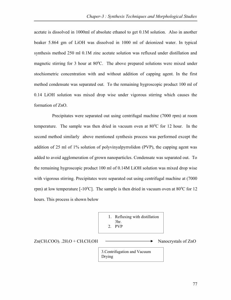
Zn(CH3COO)2 .2H2O + CH3CH2OH Nanocrystals of ZnO
77
1. Refluxing with distillation 3hr.
2. PVP
3.Centrifugation and Vacuum Drying

Chaper-3 : Synthesis Techniques and Morphological Studies
Fig 3.3 Block diagram for synthesis of various nanostructures
3.4 XRD Studies of ZnO Phosphors
3.4.1 XRD Study of ZnO Nanobelts and Nanorods
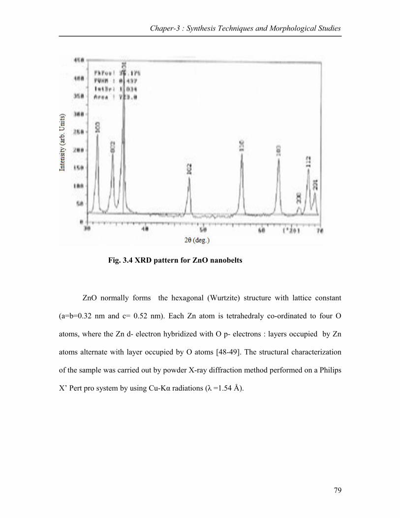
X-Ray diffraction (XRD) data for structural characterization of various prepared
samples of ZnO were collected on the X-ray diffractometer (PW1710) using Cu-Kα
(λ =1.54A0). X-ray diffraction pattern of various synthesized phosphors are helpful in
studying the crystalline structure and phase priority as well as crystallite size for
nanophosphros. The room temperature XRD patterns of synthesized ZnO phosphors
followed by various synthesis routes are shown below:
78
Chaper-3 : Synthesis Techniques and Morphological Studies
Fig. 3.4 XRD pattern for ZnO nanobelts
ZnO normally forms the hexagonal (Wurtzite) structure with lattice constant
(a=b=0.32 nm and c= 0.52 nm). Each Zn atom is tetrahedraly co-ordinated to four O
atoms, where the Zn d- electron hybridized with O p- electrons : layers occupied by Zn
atoms alternate with layer occupied by O atoms [48-49]. The structural characterization
of the sample was carried out by powder X-ray diffraction method performed on a Philips
X’ Pert pro system by using Cu-Kα radiations (λ =1.54 Å).
79
(100
)(0
02)
(101
)
(102
) (110
)
(103
)
(112
)(2
01)
(200
)
Chaper-3 : Synthesis Techniques and Morphological Studies
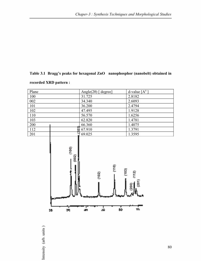
Table 3.1 Bragg’s peaks for hexagonal ZnO nanophosphor (nanobelt) obtained in
recorded XRD pattern :
Plane Angle(2θ) [ degree] d-value [A0 ]100 31.725 2.8182002 34.340 2.6093101 36.200 2.4794102 47.495 1.9128110 56.570 1.6256103 62.820 1.4781200 66.360 1.4075112 67.910 1.3791201 69.025 1.3595
80
Inte
nsity
(ar
b. u
nits
)

Chaper-3 : Synthesis Techniques and Morphological Studies
Fig. 3.5 XRD pattern for ZnO nanorods
81
2θ in degree
Chaper-3 : Synthesis Techniques and Morphological Studies
Table 3.2 Bragg’s peak of hexagonal ZnO nanorods in XRD
Plane Angle2θ[in degree] d-value [A0]100 31.520 2.7182002 34.240 2.5993101 35.980 2.4394102 47.290 1.8124110 56.570 1.6956103 62.720 1.5782200 65.450 1.4975112 67.230 1.3590201 69.025 1.3395
The XRD results showed that the as prepared product has a single hexagonal
phase . The high c-axis orientation of crystalline structure along (101) plane has been
observed. A high degree of crystal orientation reduces the probability of the scattering of
the carriers at the grain boundary.
The recorded XRD pattern confirmed that nanobelts are high crystalline in
nature. The corresponding X-ray diffraction peak for (100), (002) and (101) planes
confirm the formation of wurtzite structure of ZnO. XRD pattern for ZnO nanorods is
almost similar to the nanobelts. Compared the XRD patterns recorted for ZnO nanobelts
and nanorods as shown in Figs. 3.4 and 3.5 show that both the morphologies of ZnO
nanostructures have almost similar diffraction pattern.
The average crystallite size has been calculated from the recorded XRD pattern
using well known Scherrer equation[50 ].
D = 0.9 λ/ β λ cosθ (3.1)
82

Chaper-3 : Synthesis Techniques and Morphological Studies
λ is the X-ray wavelength used, β full width of diffraction peak at half maximum
intensity and θ is Bragg’s angle in degree. The average crystallite size comes out to be 30
nm for nanobelts.
3.4.2 XRD study of ZnO nanocrystals
X-ray diffraction peak profiles of ZnO nanopowder capped with PVP and without
PVP are shown in Fig 3.6 and 3.7. The diffraction peaks were recorded in the 2θ range
from 300 to 700 Cu-Kα (λ =1.54A0 ) radiation with a graphite monochromator in the
diffracted beam. Comparison of the recorded XRD patterns with standard JCPDS data
base file 36-1451 shows that synthesized ZnO crystallite is Wurtzite in phase.
Crystallite size was estimated by using Scherrer`s equation [50].
The crystallite size was ~ 50 nm for the sample synthesized without PVP where
as crystallite size ~ 10 nm for PVP modified has been observed. In case of PVP capped
sample broadening of diffraction peaks takes place due to lesser no planes at the surface.
The intensity of peak (002) is high as compared to other peaks showed that more oxygen
atom has entered into the ZnO film lattice.
83
Chaper-3 : Synthesis Techniques and Morphological Studies
Fig. 3.6 XRD pattern of without PVP capped ZnO nanocrystals
Table 3.3 Bragg's Peak of hexagonal ZnO nanocrystals obtained in XRD pattern :
84

Chaper-3 : Synthesis Techniques and Morphological Studies
Plane Angle(2θ) [in degree] d-value[A0 ]
100 31.485 2.8391
002 34.170 2.6219
101 36.000 2.4927
102 47.245 1.9223
110 56.280 1.6333
103 62.665 1.4813
100 66.170 1.4323
112 67.675 1.3833
201 68.800 1.3634
Fig 3.7 XRD pattern of PVP capped ZnO nanocrystals
Table 3.4 Bragg’s Peaks to hexagonal ZnO nanocrystals obtained :
Plane Angle(2θ) [in degree] d-value [A0 ]
100 32.725 2.6184
002 35.440 2.4073
101 36.200 2.1794
102 47.495 1.7124
85
2θ in degree
Inte
nsity
(arb
. uni
ts)
Chaper-3 : Synthesis Techniques and Morphological Studies
110 56.820 1.4254
3.5 Particle Size Measurement for ZnO Nanophosphors
If average crystallite size of ZnO nanoparticle is equivalent to twice of exciton
Bohr radius , quantum confinement effect is expected to occur within these nanocrystals,
exhibiting an enlargement of the optical bandgap. Increase in energy bandgap was
calculated using effective mass model. The formula used to calculate band-gap of ZnO
nano crystal is given below:
2 2 2
2
1.82 4g
o r
eE Em R Rπ
µ π ε= + −h
(3.2)
Where E is band gap of nanocrystal, Eg is the bandgap of bulk material. First
term in the relation corresponds to band gap (Eg = 3.37eV) of bulk crystal, second term is
due to quantum confinement effects and third term is related with coulomb interaction. R
is the radius of the nanoparticles which can be obtained from the XRD pattern or TEM
studies. mo is the rest mass of electron and µ is the reduced mass of the electron hole
pair. Bandgap of ZnO nanocrystal equal to 3.4 eV is calculated using effective mass
model (Eqn.3.2).
3.6 Morphological Characterization
3.6.1 Characterization of ZnO nanostructures by Scanning electron microscopic
[SEM]
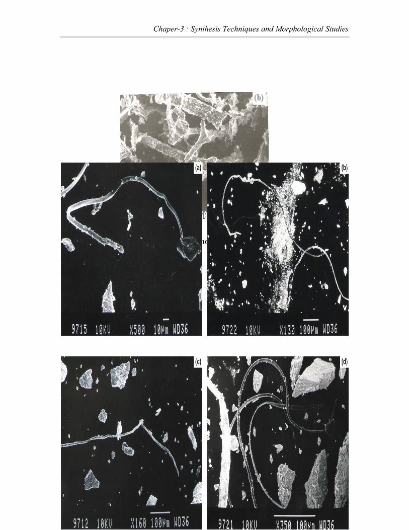
Scanning electron microscope (SEM) images of ZnO nanobelts were obtained
using JSM-6100 type microscope. It is very much clear from SEM images of synthesised
samples depend on the reaction conditions. Figs 3.8 (a & b) and 3.9 (a,b,c& d) shows
nanobelts of deformed morphologies as well as defined morphology corresponding to
86
Chaper-3 : Synthesis Techniques and Morphological Studies
synthesis methods 1 and 2, details of which have been already described in sections 3.3.1
and 3.3.2. The nanobelts obtained are of ~ 2mm in length. Refluxing of precursor
contains zinc acetates and ethanol for long time results in longer nanobelts of ZnO.
Addition of a catalyst stops isotropic agglomeration of the particle, While on the other
hand anisotropic agglomeration occur resulting in nanowire or nanobelts. The
corresponding XRD pattern also shows enhancement of (002) peak intensity, indicating
preferential growth of nanobelts along c-axis direction. SEM image at 500X
magnification indicates homogenous growth of nanobelts over large surface area as
shown in Fig 3.9. SEM image of ZnO exhibits smoother topography and long length
morphology. Scanning electron microscopy has been used to reveal the morphological
details of fabricated ZnO. The recorded micrographs revealed the uniform, very fine
structure of nanobelts which helps in trapping more light to improve solar cell efficiency
Fig 3.8 (a&b) shows the deformed morphology of the nanobelts on the other hand
Fig.3.9 (a,b,c&d) shows the well defined morphology of the nanobelts.
87
Chaper-3 : Synthesis Techniques and Morphological Studies
Fig. 3.8 (a & b) SEM images of ZnO nanobelts by method 3.3.1 (Ist method)
88

Chaper-3 : Synthesis Techniques and Morphological Studies
Fig. 3.9 (a,b,c & d) SEM images of ZnO nanobelts by method 3.3.1 (2nd method)
89
Chaper-3 : Synthesis Techniques and Morphological Studies
3.6.2 Characterization Using TEM
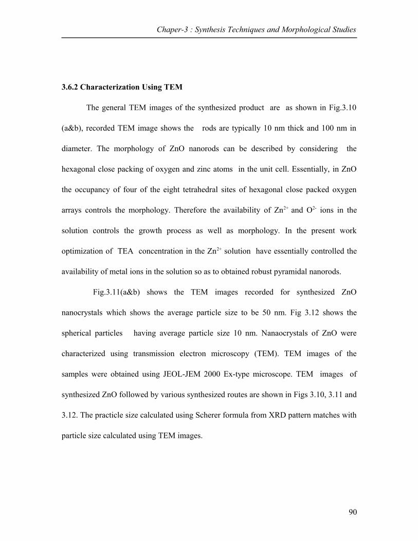
The general TEM images of the synthesized product are as shown in Fig.3.10
(a&b), recorded TEM image shows the rods are typically 10 nm thick and 100 nm in
diameter. The morphology of ZnO nanorods can be described by considering the
hexagonal close packing of oxygen and zinc atoms in the unit cell. Essentially, in ZnO
the occupancy of four of the eight tetrahedral sites of hexagonal close packed oxygen
arrays controls the morphology. Therefore the availability of Zn2+ and O2- ions in the
solution controls the growth process as well as morphology. In the present work
optimization of TEA concentration in the Zn2+ solution have essentially controlled the
availability of metal ions in the solution so as to obtained robust pyramidal nanorods.
Fig.3.11(a&b) shows the TEM images recorded for synthesized ZnO
nanocrystals which shows the average particle size to be 50 nm. Fig 3.12 shows the
spherical particles having average particle size 10 nm. Nanaocrystals of ZnO were
characterized using transmission electron microscopy (TEM). TEM images of the
samples were obtained using JEOL-JEM 2000 Ex-type microscope. TEM images of
synthesized ZnO followed by various synthesized routes are shown in Figs 3.10, 3.11 and
3.12. The practicle size calculated using Scherer formula from XRD pattern matches with
particle size calculated using TEM images.
90

(a) (b)
(a) (b)
Chaper-3 : Synthesis Techniques and Morphological Studies
Fig. 3.10 (a & b) TEM images of ZnO nanorods
Fig. 3.11 (a &b) TEM images of ZnO nanocrystals without PVP modified sample
91

Chaper-3 : Synthesis Techniques and Morphological Studies
Fig. 3.12 TEM image of ZnO nanocrystals with PVP modified sample
3.7 Results and Discussion
The morphological characterizations of the prepared ZnO nanobelts were
examined by XRD, TEM and SEM studies. High purity nanobelts of ZnO having length
in the range of few millimeters have been synthesized in the laboratory. SEM
investigations show beautiful results of ZnO nanobelts indicating the ribbon-like structure
having rectangular cross–section of these synthesized nanobelts. To the best of
knowledge, the long length nanobelts mentioned in the literature are of 0.7 nm length
[38]. ZnO nanobelt shown in Fig.3.9 is of 2.0 mm length, which is four times longer than
that reported in literature. Refluxing of precursor containing zinc acetate and ethanol for
long time results in longer nanobelts of ZnO. Addition of a catalyst stops isotropic
92

Chaper-3 : Synthesis Techniques and Morphological Studies
agglomeration of the particle instead anisotropic agglomeration occurs resulting in
nanowires or nanobelts [38]. Typical XRD pattern of ZnO nanobelts is shown in Fig. 3.4.
Lattice constant (a=b=0.32nm and c=052nm) and diffraction peaks corresponding to the
planes<100>,<002> and <101> obtained from X-Ray diffraction data confirm the
hexagon wurtzite crystal structure of zinc oxide (consistent with JCPDS data File )
nanobelts.
The crystal growth of ZnO nanostructure includes two steps: (i) nucleation
(vaporization) and (ii) growth (condensation). The shape of nanostructure (such as
rectangular cross-section, flower like, tubes etc.) is determined mainly by the synthesis
route followed, which again depends upon potential for hydrogen (pH) value of the
reactant products. After the nucleation process, pH values of a reaction determine the
number of active sites. The second step involved in the formation of nanostructure is
termed as growth which further depends on the number of active sites, more is the
number of available active sites, much larger will be the growth of nanostructure. The
hydroxide ions in an alkaline medium will be more if the pH value is greater than 7.0, the
quantities Zn(OH2) and the growth unit ([Zn(OH4)]2-, contribute respectively to
nucleation and growth of ZnO. It is well known that the pH value comes to be 12.0 when
NaOH is used as mineralize resulting in a larger quantity of zinc hydroxide and a smaller
quantity of growth unit ([Zn(OH)4]2- . Thus, during this process the quantity of
corresponding ZnO nuclei is larger but there is not enough growth unit [Zn (OH)4]2- to
grow ZnO nuclei. Moreover, there are no active sites around the circumference of ZnO
nuclei due to the limitations of increasing temperature of the reaction. Therefore, due to
anisotropic growth habit of ZnO tip like particles of ZnO will be obtained at low
93

Chaper-3 : Synthesis Techniques and Morphological Studies
temperature. However if LiOH is used instead of NaOH as a mineralize and when the pH
value of reaction is set to be 8.0 the following reaction will takes place :
Zn(OH)2 + 2OH- [Zn(OH)4 ]2-
This indicates that Zn(OH)2 not only contributes to ZnO nuclei as mentioned
above, but also transform to [Zn(OH)4 ]2- as to increase the growth of ZnO. Furthermore,
in the reaction of high temperature, active sites can generate around ZnO nuclei, so that
ZnO can preferentially be grown on the active sites. Refluxing of the ethanol, stops
isotropic agglomeration, instead anisotropic agglomeration takes place, which results in
the formation of quasi one dimensional nanobelts having rectangular cross section.
However, in this case, the number of growth units [Zn(OH)4 ]2- is still not enough to
make ZnO nanorods which are grown from the circumference of ZnO particles. But, the
flower-like ZnO nanostructure can be obtained if the pH value of the solution is increased
to 13.5,which is due to reason that a smaller quantity of Zn(OH)2 and a larger quantity
of growth unit [Zn(OH)4 ]2- are obtained. The more schematic and elaborative diagram
involving the mechanism process for synthesis of various nanostructures is as shown
below in Fig. 3.13.
The Zn ions on the top of molecule is positively charged while the bottom oxygen
ions is negatively charged, the resultant is electrostatic polarization along its surface
causing a perpendicular dipole-moment here. The electric field of the dipole creates the
dipole-moment, but when neutralized by spiraling the material achieves a lower energy
state. Using such individual nanosprings, nanosized biosensors can be made.
Piezoeleectric semiconductors are natural resonators when stimulated physically: a
piezoelectric material will naturally oscillate at a known frequency.
94

Chaper-3 : Synthesis Techniques and Morphological Studies
Fig. 3.13 Formation of ZnO nanostructures
Therefore its surface is treated to attract, for example, a protein from a cancer cell,
and then even a single molecule of that protein could be detected with one of its
nanosprings. If one can place a single molecule on the surface , change in its resonance
frequency can be detected and by determining the frequency , one can tell what molecule
is placed on the surface. With this technique cancer cell can be detected. Due to
compatibility of ZnO with human body it is best suited material for cancer cell detection.
95
Chaper-3 : Synthesis Techniques and Morphological Studies
Micro-Electro-Mechanical System (MEMS) is the integration of mechanical components,
sensors, actuators and electronic components on single chip. The ZnO can be employed
as bio-sensors in MEMS by some suitable fabrication technique.
ZnO nanomaterials are very attractive for field emission display (FEDs) which
operate with low voltage and high current density. Advantage includes high resolution
screens, enhanced lifetime at high current density and excellent thermal and mechanical
stabilities. Many researches [5-8] have studied luminescence of nanophosphors in an
attempt to improve the properties through increasing light scattering centers using surface
modification, reducing defects density by post annealing at high temperature and
identifying new phosphors material. The study of nanophosphors is useful not only for
achieving high luminescence performance, but also in understanding the fundamental
properties of the nanomaterials.
3.7.1 ZnO Nanocrystals
Different sized nanocrystals of ZnO phosphors have been synthesized using
different techniques. Their optical and morphologically studies have been done by using
optical absorptions spectroscopy (UV-Visible), X-Ray diffraction analysis (XRD image)
scanning electron microscopic (SEM) and transmission electron microscopic (TEM)
image. XRD pattern confirms hexagon, wurrtzile crystal structure of the ZnO. Lattice
constant and diffraction peaks obtained from X-ray diffraction data are consistent with
JCPDS data file no. (36-1451). The scanning electron microscopic image of ZnO tells
96

Chaper-3 : Synthesis Techniques and Morphological Studies
that the formation of nanobelts of ~ 2mm in length by changing the concentration of
LiOH as shown in Fig 3.9. The transmission electon microscopic image of nanorodes,
nanoparticles and nanobelts. The aspect ratio for the nanorods in the Fig. 3.10 (a) is of 10
and in the Fig. 3.10 (b) it is 15 , shows a drastic transmission of nanoparticles into
nanorods of average diameter 10 nm and length 100 nm. This is due to Zn2+ have led to
fast anisotropic growth of ZnO along the c-axis the [002] direction.
The TEM images in the Figs.3.11(a& b) and 3.12 shows that the particle size of
50 nm and 10 nm are obtained, This difference in particle size is due to the difference of
the capping agent which help in formation of a small size particle spherical in shape. The
XRD pattern for the ZnO nanoparticle and one dimension nanorods are shown in Fig
3.5,3.6, and3.7, the X-ray diffraction peak for a well crystalline hexagonal Wurtzite ZnO
structure. In comparison the diffraction peaks for the nanoparticles are broadened than
those of nanorods. In addition nanorods spectrum shows a sharp diffraction peaks. This is
constituent with one dimension nanorods formation along c-axis [52-53]. The TEM
image tells that the particle size for the ZnO nanocrystal is of 10 nm and was confirmed
by Scherer formula (~ 10 nm) using XRD data of ZnO nanocrystals.
3.8 Conclusions
High purity nanobelts , nanorods and nanoparticles of ZnO have been synthesized
in the laboratory by controlling the reaction time and the concentration of LiOH type
applied method is simple and reproductive for variety of nanostructure on a potentially
97

Chaper-3 : Synthesis Techniques and Morphological Studies
large synthetic scale. The nanoparticles are driven to be arranged in linear fashion to form
one dimension naorods. Structural analysis shows that typical diffraction peaks for
nanoparticles, naorods and nanobelts of well crystalline hexagonal ( Wurtzite ) structure
of ZnO. The nanostructure of ZnO synthesized using various techniques are characterized
using XRD, SEM, TEM. Scanning electron microscope and transmission electron
microscope image of ZnO indicate the size of various ZnO crystals. The size obtained
from TEM image is agreement well with Scherrer formula.
98

Chaper-3 : Synthesis Techniques and Morphological Studies
Refrences
[1] C.B Murray, D.J. Norris and M.G. Bawendi, J. Am.Chem.Soc., 115, 8706 (1993).
[2] D.O. Dabbouusi, J.R Viejo, F.V. Mikulec, J.R. Heine, H. Mattoussi, R. Ober,K.F.
Jensen and M.G. Bawendi, J.Phys.Chem.B, 101, 9463 (1997).
[3] K. Manzoor, S.R. Vadera, N.Kumar and T.R. Kutty, J.Mater.Chem.Phys., 82, 718
(2003).
[4] W.E. Lynch, D.A. Nivens and B.C. Helmy, J.The Chem.Edu., 9,159 (2004).
[5] H.S.Bhatti, R.Sharma, N.K.Verma, N.Kumar, S.R. Vadera and K.Manzoor
J.Phys.D:Appl.Phys., 39, 1754 (2006).
[6] F.V.Mikulec, M. Kuno, M. Bennani , D.A. Hall, R.G Griffin and M.G. Bawndi,
J.Am. Chem.Soc., 122, 2532 (2000)
[7 ] H.S.Bhatti, K.Singh, S.Kumar and N.K.Verma J.Nanopart.Res. 11, 1017 (2009).
[8] Z. Li, Y. Xiong and Y. Xie, J.Inorg.Chem., 42, 8105 (2004).
[9] H. Yan , R. He, J. Johnson, M. Law, R. Saykally and P. Yang J.Am.Chem.soc.,
125 , 4728 (2007).
[10] D.J.Norris, N. Yao, F.T. Charnock and T.A. Kennedy, J. Nano. Lett. 1, 3 (2001)
[11] M.Huang, S Mao, H Fieck, H. Yan, Y Wu, H Kind, E Weber , R Russo and P
Yang, Science 292, 1897 (2001).
[12] P.Yang, H Yan, S Mao, R Russo, J Johnson , R Saykally,N Morris, J Phan , R He
and Choi J. Adv. Funct.Mater., 12, 323 (2002).
[13] W. Z. Pan , R. Z. Dai and Z. L. Wang, Science, 291,1947 (2009)
[14] X. Y. Kong, Y. Ding, R. Yang and Z. Wang, Science 303, 1348 (2004).
[15] X. Dai, Y, Zhang, Y, Bai and Z. Wang, J. Chem.Phys.Lett., 96, 375 (2003).
99
Chaper-3 : Synthesis Techniques and Morphological Studies
[16] B. Geng, G. Wang, Z. Jiang, T. Xie, S. Sun, G. Meng and L. Zhang, J.Appl.
Phys. Lett., 83, 4791 (2008).
[17] J. Jie, G. Wang, X. Han, Q. Yu, Y. Liao, G. Li and J. Hou, J.Chem.Phys.Lett., 38,
7466 (2007).
[18] M.P.Pileni, J. Phys.Chem., 97, 6961 (1993).
[19] J.Cizeron and M.P. Pileni, J. Phys.Chem.B., 101, 8887 (1997).
[20] J.Dhanraj, R.Jagannathan and T.R. Kutty, J. Phys. Chem.B: 105, 11098 (2001).
[21] M.V. Artemyev, L.I. Gurinovich, A.P. Stupak and S.V. Gaponenko,
J.Phys.Stat.Solidi., 224, 191 (2001).
[22] E.M. Wong and P.C.Searson, J.Appl. Phys.Lett., 74, 2939 (1999).
[23] C. Chun, J. Rho, K. Lee, S. Joo and S.Taiha J. Appl.Phys. Lett., 10, 093117
(2009).
[24] W.Z. Pan , R.Z. Dai and Z.L. Wang, Science, 291, 1947 (2001).
[25] J.Y. Lao, J.Y. huang, D.Z. Wang, Z.F. Ren, Nanotechnology Lett., 3, 235 (2003).
[26] C.Gao, P.X.Ding, Y.Wang and Z.L. Schwen J.Appl.Phys. Lett., 84, 092127
(2009).
[27] M.K.Yadav, M. Ghosh, A. Mookerjee and S. Datta J.Phys. Rev. B: 76, 045223
(2009).
[28] B.B. Lakshmi, C.J.Partrissi and C.R. Martin, J.Chem. Mater., 9, 2544 (1997).
[29] H.Zhang, X.Y. Ma, J. Xu, J.J.Niu and D.R. Yang, Nanotechnology, 14, 423
(2003).
[30] J.Zhang, W.Yu, L.Zhang, J.Phys. Lett. A:, 299, 276 (2002).
[31] Q.Qu, T. Matsuda, M. Mesko and M. Nagatsu. J.Mater. Lett., 60, 3122 (2008).
100

Chaper-3 : Synthesis Techniques and Morphological Studies
[32] Z.L.Wang, R.P.Gao, Z.W. Pan and Z.R.Dai, J.Adv. Eng. Mater., 3, 657 (2001).
[33] Z.R.Dai, Z.W. Pan and Z.L.Wang, J.Solid State Commun., 118, 351 (2001).
[34] K.J. Albert, N.S. Lewis, C.L.Schauer, G.A.Sotzing, S.E.Stitzel, T.P. Vaid and
D.R. Walt, J.Chem. Rev., 100, 2595 (2000).
[35] Z.K. Yang, P. Yu, G.K.L. Wong, M. Kawasaki., A. Ohtomo, H. Koinuma and Y.
Segawa, J.Solid State Commun., 103, 459 (1997).
[36] A. Ohtomo, M. Kawasaki, I. Ohkubo, H. Koinuma, T. Yasuda and Y. Segawa,
J.Appl. Phys.Lett., 75, 980 (1999).
[37] X.Gang, J.Wilkinson, J.Lyles, K.B.Ucer and R.T. Williams, J. Rad. Effect Defect.
Solid., 158, 83 (2003).
[38] H.Cao, J.Y. Xu, D.Z.Zhang, S.H.Chang, S.T.Ho, E.W.Seelig ,X.Liu X and R.P.H.
Chang, J. Phys. Rev.Lett., 84, 5584 (2000).
[39] H.Cao, J.Y.Xu, Y. Ling, A.L.Burin, X.Liu, E.W.Seeling, X.Liu and R.P.H.
Chang, J. Quantum Electron., 9, 111 (2003).
[40] L.Spanhel and M.R.Anderson, J.Am.Chem.Soc., 113, 2826 (1991).
[41] M.K. Hossain, S.C. Ghosh, Y. Boontongkong, C. Thanachayanont and J. Dutta,
International conference on Materials for advanced Technologies, Singapore,
December 7-12 (2003)
[42] M.K. Hossain, S.C. Ghosh, Y. Boontongkong, C. Thanachayanont and J. Dutta,
J.Metas. Nanocryst. Mater., 23, 27 (2005).
[43] H.S. Bhatti, A.Gupta, N.K.Verma and S.Kumar, J.Mater.Sci.: Mater. Electron.,
17, 281 (2006).
[44] T.Hirano and H. Kozuka, J.Mater. Sci., 38, 4203 (2003).
101

Chaper-3 : Synthesis Techniques and Morphological Studies
[45] H.J.Leel, B.S.Kim, C.R.Cho and S.Y. Jeong, J.Phys.Stat.Solid. B: 241, 1533
(2004).
[46] S.Chakrabarti, D. Ganguli and S. Chaudhuri, J. Phys. D: Appl. Phys., 36, 146
(2003).
[47] N.Ohashi, N.Ebsisawa, T. Sekiguchi, i.Sakaguchi, Y. Wada, T. Takenaka and H.
Haneda, J.Appl.Phys.Lett., 86, 91902 (2005).
[48] H.S.Bhatti, K.Singh and N.K.Verma, J.Mater.Sci:Mater.Electron, 20, 255 (2009).
[49] H.S.Bhatti, D.Kumar, A.Gupta, R.Sharma, K.Singh and P.Sharma,
J.Opto.electro.Adv. Mater., 8, 860 (2006).
[50] B.D. Cullity, Elements of X-ray diffraction, Addison- Wesley, Massachusetts,
102 (1978).
[51] M.Joseph, H. Tobata and T.Kawai, J.Appl.Phys. Lett., 74, 2534 (1999).
[52] S . Seow, W. Wong, V. Thavasi, R.Jose and S. RamaKrishna, Nanotechnology
20, 045604 (2009).
[53] H.S.Bhatti, A.Gupta, N.K. Verma and S. Kumar J.Phy. and Chem.Solids, 67, 868
(2006)
102