Chalmers Publication Librarypublications.lib.chalmers.se/records/fulltext/local_145958.pdf · ......
17
Chalmers Publication Library Copyright Notice This paper was published in Optics Express and is made available as an electronic reprint with the permission of OSA. The paper can be found at the following URL on the OSA website: http://dx.doi.org/10.1364/OE.19.015490. Systematic or multiple reproduction or distribution to multiple locations via electronic or other means is prohibited and is subject to penalties under law. (Article begins on next page)
Transcript of Chalmers Publication Librarypublications.lib.chalmers.se/records/fulltext/local_145958.pdf · ......

Chalmers Publication Library
Copyright Notice
This paper was published in Optics Express and is made available as an electronic reprint with the permission of OSA. The paper can be found at the following URL on the OSA website: http://dx.doi.org/10.1364/OE.19.015490. Systematic or multiple reproduction or distribution to multiple locations via electronic or other means is prohibited and is subject to penalties under law.
(Article begins on next page)

Assessment of VCSEL thermal rollovermechanisms from measurements and
empirical modeling
Prashant P. Baveja,1,2,∗ Benjamin Kogel,2 Petter Westbergh,2 Johan S.Gustavsson,2 Asa Haglund,2 Drew N. Maywar,3 Govind P. Agrawal,1
and Anders Larsson2
1The Institute of Optics, University of Rochester, Rochester, NY, 14627 USA2Department of Microtechnology and Nanoscience, Photonics Laboratory, Chalmers
University of Technology, Goteborg SE-412 96, Sweden3Electrical, Computer and Telecommunications Engineering Technology Dept., Rochester
Institute of Technology, Rochester, NY 14623, USA∗[email protected]
Abstract: We use an empirical model together with experimentalmeasurements for studying mechanisms contributing to thermal rolloverin vertical-cavity surface-emitting lasers (VCSELs). The model is basedon extraction of the temperature dependence of threshold current, internalquantum efficiency, internal optical loss, series resistance and thermalimpedance from measurements of output power, voltage and lasing wave-length as a function of bias current over an ambient temperature rangeof 15-100◦C. We apply the model to an oxide-confined, 850-nm VCSEL,fabricated with a 9-μm inner-aperture diameter and optimized for high-speed operation, and show for this specific device that power dissipationdue to linear power dissipation (sum total of optical absorption, carrierthermalization, carrier leakage and spontaneous carrier recombination)exceeds power dissipation across the series resistance (quadratic powerdissipation) at any ambient temperature and bias current. We further showthat the dominant contributors to self-heating for this particular VCSELare quadratic power dissipation, internal optical loss, and carrier leakage.A rapid reduction of the internal quantum efficiency at high bias currents(resulting in high temperatures) is identified as being the major cause ofthermal rollover. Our method is applicable to any VCSEL and is useful foridentifying the mechanisms limiting the thermal performance of the deviceand to formulate design strategies to ameliorate them.
© 2011 Optical Society of America
OCIS codes: (250.7260) Vertical cavity surface emitting lasers; (140.6810) Thermal effects;(200.4650) Optical interconnects; (230.1150) All-optical devices; (060.4510) Optical commu-nications.
References and links1. W. Hofmann, “High-speed buried tunnel junction vertical-cavity surface-emitting lasers,” IEEE Photon. J. 2,
802–815 (2010).2. R. Safaisini, J. R. Joseph, and K. L. Lear, “Scalable high-CW-power high-speed 980-nm VCSEL arrays,” IEEE
J. Quantum Electron. 46, 1590–1596 (2010).3. P. Westbergh, J. Gustavsson, A. Haglund, M. Skold, A. Joel, and A. Larsson, “High speed, low-current-density
850 nm VCSELs,” IEEE J. Sel. Top. Quantum Electron. 15, 694–703 (2009).
#147763 - $15.00 USD Received 23 May 2011; revised 4 Jul 2011; accepted 11 Jul 2011; published 28 Jul 2011(C) 2011 OSA 1 August 2011 / Vol. 19, No. 16 / OPTICS EXPRESS 15490

4. J. S. Harris, T. O’Sullivan, T. Sarmiento, M. M. Lee, and S. Vo, “Emerging applications for vertical cavity surfaceemitting lasers,” Semicond. Sci. Technol. 26, 014010 (2011).
5. B. Ciftcioglu, R. Berman, J. Zhang, Z. Darling, S. Wang, J. Hu, J. Xue, A. Garg, M. Jain, I. Savidis, D. Moore,M. Huang, E. G. Friedman, G. Wicks, and H. Wu, “A 3-D integrated intrachip free-space optical interconnect formany-core chips,” IEEE Photon. Technol. Lett. 23, 164–166 (2011).
6. I. A. Young, E. M. Mohammed, J. T. S. Liao, A. M. Kern, S. Palermo, B. A. Block, M. R. Reshotko, and P. L. D.Chang, “Optical technology for energy efficient I/O in high performance computing,” IEEE Commun. Mag. 48,184–191 (2010).
7. Y. Ding, W. J. Fan, D. W. Xu, C. Z. Tong, Y. Liu, and L. J. Zha, “Low threshold current density, low resistanceoxide-confined VCSEL fabricated by a dielectric-free approach,” Appl. Phys. B 98, 773–778 (2010).
8. A. Haglund, J. S. Gustavsson, J. Vukussic, P. Modh, and A. Larsson, “Single fundamental-mode output powerexceeding 6 mW from VCSELs with a shallow surface relief,” IEEE Photon. Technol. Lett. 16, 368–370 (2004).
9. C. Ji, J. Wang, D. Soderstrom, and L. Giovane, “20-Gb/s 850-nm oxide VCSEL operating at 25◦C-70◦C,” IEEEPhoton. Technol. Lett. 22, 670–672 (2010).
10. P. Westbergh, J. S. Gustavsson, B. Kogel, A. Haglund, and A. Larsson, “Impact of photon lifetime on high speedVCSEL performance,” IEEE J. Sel. Top. Quantum Electron. (accepted for publication).
11. A. N. Al-Omari and K. L. Lear, “VCSELs with a self-aligned contact and copper-plated heatsink,” IEEE Photon.Technol. Lett. 17, 1225–1227 (2005).
12. Y. Ou, J. S. Gustavsson, P. Westbergh, A. Haglund, A. Larsson, and A. Joel, “Impedance characteristics andparasitic speed limitations of high-speed 850-nm VCSELs,” IEEE Photon. Technol. Lett. 21, 1840–1842 (2009).
13. Y.-C. Chang and L. A. Coldren, “Efficient, high-data-rate, tapered oxide-aperture, vertical-cavity surface-emitting lasers,” IEEE J. Sel. Top. Quantum Electron. 15, 1–12 (2009).
14. A. N. Al-Omari and K. L. Lear, “Polyimide-planarized vertical-cavity surface-emitting lasers with 17.0-GHzbandwidth,” IEEE Photon. Technol. Lett. 16, 969–971 (2004).
15. S. B. Healy, E. P. O’Reilly, J. S. Gustavsson, P. Westbergh, A. Haglund, A. Larsson, and A. Joel, “Active regiondesign for high-speed 850-nm VCSELs,” IEEE J. Quantum Electron. 46, 506–512 (2010).
16. Y. Liu, W.-C. Ng, K. D. Choquette, and K. Hess, “Numerical investigation of self-heating effects of oxide-confined vertical-cavity surface-emitting lasers,” IEEE J. Quantum Electron. 41, 15–25 (2005).
17. P. V. Mena, J. J. Morikuni, S.-M. Kang, A. V. Harton, and K. W. Wyatt, “A simple rate-equation-based thermalVCSEL model,” J. Lightwave Technol. 17, 865–872 (1999).
18. J. W. Scott, R. S. Geels, S. W. Corzine, and L. A. Coldren, “Modeling temperature effects and spatial holeburning to optimize vertical-cavity surface-emitting laser performance,” IEEE J. Quantum Electron. 29, 1295–1308 (1993).
19. G. Hasnain, K. Tai, L. Yang, Y. H. Wang, R. J. Fischer, J. D. Wynn, B. Weir, N. K. Dutta, and A. Y. Cho,“Performance of gain-guided surface emitting lasers with semiconductor distributed bragg reflectors,” IEEE J.Quantum Electron. 27, 1377–1385 (1991).
20. W. Nakwaski and M. Osinski, “On the thermal resistance of vertical-cavity surface-emitting lasers,” Opt. Quan-tum Electron. 29, 883–892 (1997).
21. P. Debernardi, A. Kroner, F. Rinaldi, and R. Michalzik, “Surface relief versus standard VCSELs: A comparisonbetween experimental and hot-cavity model results,” IEEE J. Sel. Top. Quantum Electron. 15, 828–837 (2009).
22. C. Wilmsen, H. Temkin, and L. Coldren, Vertical-Cavity Surface-Emitting Lasers: Design, Fabrication, Charac-terization, and Applications, (Cambridge Univ. Press, 1999).
23. C. J. Chang-Hasnain, C. E. Zah, G. Hasnain, J. P. Harbison, L. T. Florez, N. G. Stoffel, and T. P. Lee, “Effect ofoperating electric power on the dynamic behavior of quantum well vertical-cavity surface-emitting lasers,” Appl.Phys. Lett. 58, 1247–1249 (1991).
24. W. H. Knox, D. S. Chemla, G. Livescu, J. E. Cunningham, and J. E. Henry, “Femtosecond carrier thermalizationin dense fermi seas,” Phys. Rev. Lett. 61, 1290–1293 (1988).
25. L. A. Coldren and S. W. Corzine, Diode Lasers and Photonic Intergrated Circuits (Wiley, 1995).26. Y.-A. Chang, J.-R. Chen, H.-C. Kuo, Y.-K. Kuo, and S.-C. Wang, “Theoretical and experimental analysis on
InAlGaAs/AlGaAs active region of 850-nm vertical-cavity surface-emitting lasers,” J. Lightwave Technol. 24,536–543 (2006).
27. I. Vurgaftman, J. R. Meyer, and L.-R. Ram-Mohan, “Band parameters for III-V compound semiconductors andtheir alloys,” Appl. Phys. Rev. 89, 5815–5875 (2001).
28. D. V. Kuksenkov, H. Temkin, and S. Swirhun, “Measurement of internal quantum efficiency and losses in verticalcavity surface emitting lasers,” Appl. Phys. Lett. 66, 1720–1722 (1995).
29. G. R. Hadley, “Effective index model for vertical-cavity surface-emitting lasers,” Opt. Lett. 20, 1483–1485(1995).
30. A. Larsson, P. Westbergh, J. Gustavsson, A. Haglund, and B. Kogel, “High-speed VCSELs for short reach com-munication,” Semicond. Sci. Technol. 26, 014017 (2011).
31. L. F. Lester, S. S. O’Keefe, W. J. Schaff, and L. F. Eastman, “Multiquantum well strained-layer lasers withimproved low frequency response and very low damping,” Electron. Lett. 28, 383–385 (1992).
32. K. L. Lear and R. P. Schneider, Jr., “Uniparabolic mirror grading for vertical cavity surface emitting lasers,” Appl.
#147763 - $15.00 USD Received 23 May 2011; revised 4 Jul 2011; accepted 11 Jul 2011; published 28 Jul 2011(C) 2011 OSA 1 August 2011 / Vol. 19, No. 16 / OPTICS EXPRESS 15491

Phys. Lett. 68, 605–607 (1996).33. Y.-A. Chang, T.-S. Ko, J.-R. Chen, F.-I Lai, C.-L. Yu, I.-T. Wu, H.-C. Kuo, Y.-K. Kuo, L.-W. Laih, L.-H. Laih,
T.-C. Lu, and S.-C. Wang, “The carrier blocking effect on 850 nm InAlGaAs/AlGaAs vertical-cavity surface-emitting lasers,” Semicond. Sci. Technol. 21, 1488–1494 (2006).
1. Introduction
Vertical-cavity surface-emitting lasers (VCSELs) are key components for communication andsensing applications due to their ease of fabrication and testing, low-power consumption, highbeam quality, and high modulation speeds [1–3]. In particular, VCSELs operating in the 850-nm wavelength band constitute an important class of VCSELs. This can be attributed to theavailability of commercial multimode fibers that employ VCSELs operating near 850 nm forshort-haul communication links in data centers and high-performance computing systems. Fur-ther, such VCSELs have shown the potential to play an important role in future high speedoptical interconnects and consumer electronics [3–6].
Current-induced self-heating of VCSELs has been identified as a major factor limiting theirstatic [7, 8] and dynamic performance [3, 9, 10]. Self-heating manifests itself as the prematuresaturation of the output power with increasing bias current, under continuous-wave (CW) oper-ation. Subsequent saturation of the photon density in the active region limits VCSEL’s modula-tion speed. The phenomena responsible for self-heating have received a great deal of attention,both experimentally [11–15] and theoretically [15–21]. Experimental studies on improving thethermally-limited dynamic performance have focused on reducing resistance [3, 12, 14], inter-nal optical absorption [10] and thermal impedance [11]. Theoretical modeling of self-heatingeffects is a complex problem and involves taking into account various optical, electrical andthermal interactions for the specific VCSEL design under consideration [16, 20, 21].
Previously used thermal models either address the electrical aspects of self-heating effectsthrough an equivalent electrical circuit [17] or employ a detailed physical model by incorpo-rating spatial hole burning, carrier diffusion, and surface recombination [18]. Combined withthe laser rate equations, the electrical circuit approach can predict dynamic VCSEL charac-teristics with appreciable accuracy. However, it uses higher-order polynomials to describe theV-I characteristics, and multiple measurements are required to extract values of all parametersassociated with such a model. Moreover, it provides little insight into VCSEL design opti-mization for improving thermal performance. The model of Scott et al. is important from thestandpoint of physical understanding as it incorporates microscopic details of various relevantprocesses [18]. However, it requires the knowledge of a large number of parameters whosevalues may not precisely be known for a specific VCSEL, and it also needs to be modifieddepending on the current injection mechanism. There is, therefore, a need for a generic empir-ical model which, when coupled with data from basic measurements, can identify major heatsources and quantify their contributions to the total heat load and also relate them to the VCSELdesign parameters. Such a model will be useful not only for predicting thermal performance ofa VCSEL, but also for providing design guidelines capable of enhancing the thermally-limiteddevice performance.
In this paper, we develop an empirical model to study self-heating effects in VCSELs. Themodel incorporates the temperature dependence of different macroscopic VCSEL parameters(such as series resistance, threshold current, thermal impedance, internal optical loss, and inter-nal quantum efficiency). We extract this temperature dependence from measurements of outputoptical power Popt, bias voltage Vb, and emission wavelength λ of the fundamental mode as afunction of bias current Ib over an ambient temperature range of 15-100◦C and calculate var-ious contributions to self-heating responsible for an increase in the device temperature. Theparameters are extracted by performing reliable single-parameter numerical fits to the measure-
#147763 - $15.00 USD Received 23 May 2011; revised 4 Jul 2011; accepted 11 Jul 2011; published 28 Jul 2011(C) 2011 OSA 1 August 2011 / Vol. 19, No. 16 / OPTICS EXPRESS 15492

ments. We apply this model to an oxide-confined 850-nm VCSEL, fabricated with a 9-μminner-aperture diameter and optimized for high speed operation. At room temperature (25◦C),as the bias current is increased from threshold to thermal rollover, the saturation of the outputpower is caused by a 70◦C rise in the internal device temperature, which causes the thresholdcurrent and internal optical loss to increase by 85% and 43%, respectively, and the internalquantum efficiency to decrease by 20%. Further, for this particular device, at any ambient tem-perature and bias current, linear power dissipation exceeds the quadratic power dissipation. Inaddition to quadratic power dissipation, internal optical loss and carrier leakage are the mainfactors limiting the thermal performance. Our method can potentially be applied to any VCSELdesign to pin-point the factors limiting the thermal performance and assess the impact of stepstaken to ameliorate them.
The remainder of the paper is organized as follows. In Section 2, we present the theoreticalmodel and outline the method used to extract the temperature dependence of the basic VCSELparameters. In Section 3, we briefly describe the device under test and the experimental setup.We then present results from measurements over a range of 15-100◦C and the extracted tem-perature dependence of the VCSEL parameters. The simulation results and their comparisonwith measured data are presented in Section 4. The analysis of thermal rollover mechanisms ispresented in Section 5, and the results are summarized in Section 6.
2. Theoretical Model
2.1. Modeling Thermal Effects
There are several mechanisms by which power is dissipated inside a VCSEL [21, 22]. Thepower dissipated across its series resistance Rs causes resistive or Joule heating. We refer tothis mechanism as quadratic power dissipation (QPD), as its dependence on bias current isquadratic, and include it in our model using
PQPD = Rs(Ta, Ib)I2b . (1)
where Ib is the bias current and Ta is the ambient temperature. We have included a direct de-pendence of series resistance on current caused by charge accumulation at the hetero-interfacesin the distributed Bragg reflectors (DBRs); it leads to a reduction in resistance with bias cur-rent [19, 23].
Other sources of power dissipation, including carrier leakage, carrier thermalization, spon-taneous carrier recombination, and internal optical loss linearly depend on Ib, both below andabove the threshold. We refer to the the sum of these mechanisms as linear power dissipation(LPD) and include it through
PLPD = K(T )Ib. (2)
where K(T ) is the LPD coefficient whose value also depends on the device temperature, andtherefore on both ambient temperature and current. In these equations, T = Ta + ΔT is thesum of the ambient temperature Ta and the increase in temperature ΔT caused by bias currentinduced self-heating. Henceforth, we define the value of a particular device parameter at a fixedTa and Ib unless specified otherwise.
To model PLPD, it is important to understand the physical process behind each of the con-stituent LPD mechanisms. Figure 1 schematically depicts the capture and leakage of carriersinjected into the active region of a VCSEL. Our model assumes that a fraction ηi (the internalquantum efficiency) of charge carriers carried by the bias current Ib is captured by the quantumwells; remaining carriers, which constitute carrier leakage, recombine in the barriers and the
#147763 - $15.00 USD Received 23 May 2011; revised 4 Jul 2011; accepted 11 Jul 2011; published 28 Jul 2011(C) 2011 OSA 1 August 2011 / Vol. 19, No. 16 / OPTICS EXPRESS 15493
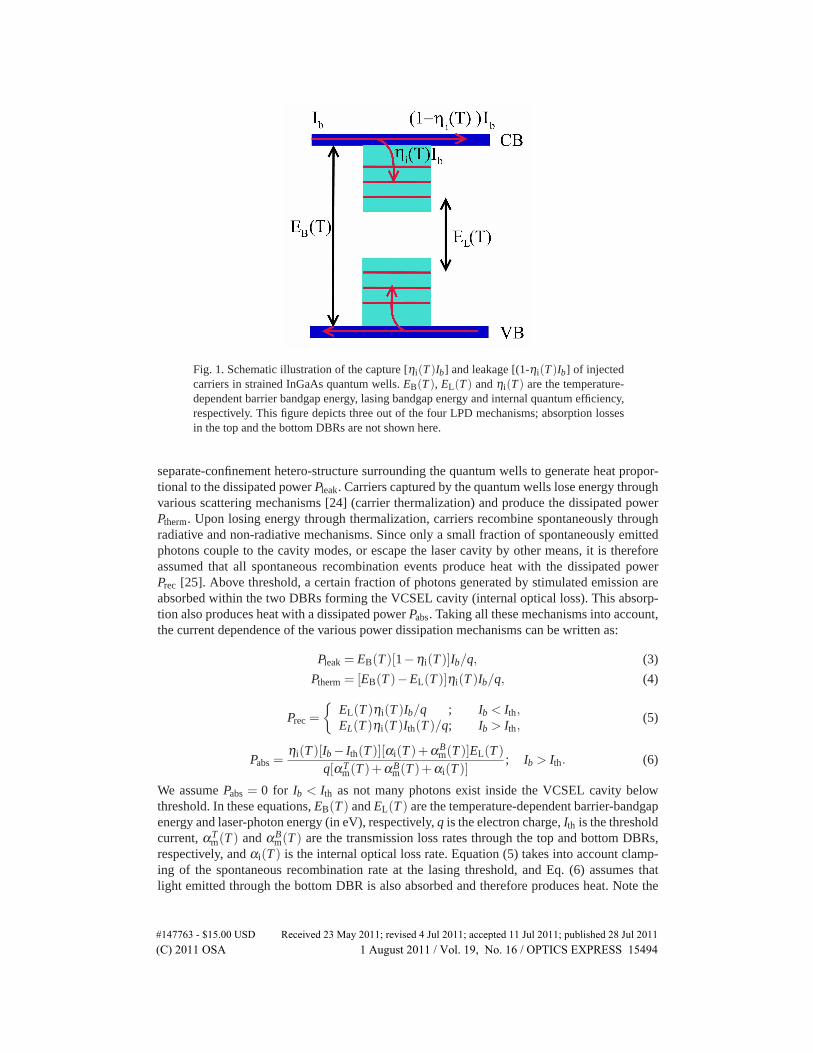
Fig. 1. Schematic illustration of the capture [ηi(T )Ib] and leakage [(1-ηi(T )Ib] of injectedcarriers in strained InGaAs quantum wells. EB(T ), EL(T ) and ηi(T ) are the temperature-dependent barrier bandgap energy, lasing bandgap energy and internal quantum efficiency,respectively. This figure depicts three out of the four LPD mechanisms; absorption lossesin the top and the bottom DBRs are not shown here.
separate-confinement hetero-structure surrounding the quantum wells to generate heat propor-tional to the dissipated power Pleak. Carriers captured by the quantum wells lose energy throughvarious scattering mechanisms [24] (carrier thermalization) and produce the dissipated powerPtherm. Upon losing energy through thermalization, carriers recombine spontaneously throughradiative and non-radiative mechanisms. Since only a small fraction of spontaneously emittedphotons couple to the cavity modes, or escape the laser cavity by other means, it is thereforeassumed that all spontaneous recombination events produce heat with the dissipated powerPrec [25]. Above threshold, a certain fraction of photons generated by stimulated emission areabsorbed within the two DBRs forming the VCSEL cavity (internal optical loss). This absorp-tion also produces heat with a dissipated power Pabs. Taking all these mechanisms into account,the current dependence of the various power dissipation mechanisms can be written as:
Pleak = EB(T )[1−ηi(T )]Ib/q, (3)
Ptherm = [EB(T )−EL(T )]ηi(T )Ib/q, (4)
Prec =
{EL(T )ηi(T )Ib/q ; Ib < Ith,EL(T )ηi(T )Ith(T )/q; Ib > Ith,
(5)
Pabs =ηi(T )[Ib − Ith(T )][αi(T )+αB
m(T )]EL(T )q[αT
m(T )+αBm(T )+αi(T )]
; Ib > Ith. (6)
We assume Pabs = 0 for Ib < Ith as not many photons exist inside the VCSEL cavity belowthreshold. In these equations, EB(T ) and EL(T ) are the temperature-dependent barrier-bandgapenergy and laser-photon energy (in eV), respectively, q is the electron charge, Ith is the thresholdcurrent, αT
m(T ) and αBm(T ) are the transmission loss rates through the top and bottom DBRs,
respectively, and αi(T ) is the internal optical loss rate. Equation (5) takes into account clamp-ing of the spontaneous recombination rate at the lasing threshold, and Eq. (6) assumes thatlight emitted through the bottom DBR is also absorbed and therefore produces heat. Note the
#147763 - $15.00 USD Received 23 May 2011; revised 4 Jul 2011; accepted 11 Jul 2011; published 28 Jul 2011(C) 2011 OSA 1 August 2011 / Vol. 19, No. 16 / OPTICS EXPRESS 15494

temperature dependence, and consequently the bias current dependence, of most parameters inEqs. (3)–(6).
When AlGaAs is used as the barrier material in 850 nm VCSELs, the temperature depen-dence of the barrier bandgap EB(T ) is determined from the Varshini equations [26, 27] for thetemperature dependence of the direct bandgap of AlAs and GaAs:
Eg(AlAs) = 3.099− 0.885×10⁻³T 2k
Tk +530, Eg(GaAs) = 1.519− 0.5405×10⁻³T 2
k
Tk +204. (7)
where Tk is the device temperature in Kelvin. The interpolation formula for the barrier bandgapof AlxGa1−xAs is known to be [27]:
Exg(AlxGa1−xAs) = xEg(AlAs)+(1− x)Eg(GaAs)− x(1− x)(−0.127+1.310x). (8)
Temperature dependence of the photon energy EL is estimated from temperature dependenceof the lasing wavelength of the fundamental LP01 mode.
Above lasing threshold, where self-heating becomes significant, the total PLPD can be writtenas
PLPD = Ptherm +Prec +Pleak +Pabs (9)
=1q
EB(T )Ib − 1q
EL(T )ηi(T )[Ib − Ith(T )]
[1− αi(T )+αB
m(T )αi(T )+αT
m(T )+αBm(T )
].
The total dissipated power (Ptot) is thus given by
Ptot = PQPD +PLPD =dVb(T, Ib)
dIbI2b +PLPD, (10)
where the series resistance has been replaced by the differential resistance (Rs = dVb/dIb) at thegiven bias point and Vb denotes the applied voltage. The device temperature T , is subsequentlyobtained using the thermal impedance Rth which relates the change in device temperature to thedissipated power and can be written as [3, 17]
T = Ta +ΔT = Ta +Rth(T )Ptot. (11)
Note that Rth also depends on temperature through temperature dependence of the thermalconductivities of various materials in the VCSEL structure [20]. We stress that the series (ordifferential) resistance in Eq. (1) and the linear power dissipation coefficient in Eq. (2) dependstrongly on temperature, and therefore also on the bias current. The consequences of this arestrong deviations from quadratic and linear dependencies of PQPD and PLPD, respectively, onthe bias current for the VCSELs operating under continuous bias current.
Finally, we calculate the optical power emitted through the top DBR, at a given current andambient temperature, using [25]:
P(T, Ib) =ηi(T )[Ib − Ith(T )]αT
m(T )αT
m(T )+αBm(T )+αi(T )
(hc
qλ (T )
). (12)
where λ (T ) is the emission wavelength of the fundamental mode, c is the speed of light and his the Planck constant.
#147763 - $15.00 USD Received 23 May 2011; revised 4 Jul 2011; accepted 11 Jul 2011; published 28 Jul 2011(C) 2011 OSA 1 August 2011 / Vol. 19, No. 16 / OPTICS EXPRESS 15495

2.2. Extraction of parameters from measurements
In the preceding analysis, we derived the equations used to relate the dissipated power Ptot,device temperature T , and output power Popt to the bias current. These equations contain anumber of parameters whose temperature dependence needs to be quantified. To achieve this,we measure the output power, voltage and emission wavelength as a function of the bias currentover a range of Ta (15-100 ◦C). The measurements are performed under continuous or low-duty-cycle pulsed operation.
The measurements for extracting the temperature dependence of VCSEL parameters are per-formed over a range of bias currents close to the lasing threshold. Any bias current-inducedincrease in temperature, ΔT , depends on the ambient temperature Ta owing to the temperaturedependence of thermal impedance [Eq. (11)] and the increasing difficulty faced in stabilizinghigh stage temperatures against room temperature. At low ambient temperatures (Ta ≤ 50◦C),the error in the extracted parameter values corresponds to a bias current induced increase in thedevice temperature (ΔT ≤ 2◦C). As discussed in the next section, this corresponds to the reso-lution limit of the device thermometer [3]. With increasing ambient temperature, ΔT increases.The corresponding errors in the reported parameter values at room temperature (Ta = 25◦C) aresummarized in Tables 1 and 2, assuming a worst-case value of 5◦C uncertainty at Ta = 100◦C.
The temperature dependence of the emission wavelength, λ (T ), is found by measuring thewavelength of the fundamental mode (LP01) as a function of ambient temperature [3]. ForGaAs-based 850-nm VCSELs, the value of Δλ/ΔT is typically around 0.06 nm/◦C. This quan-tity is also used to estimate the device temperature at various values of Ta and Ib.
The temperature dependence of the threshold current, Ith(T ), is extracted from power versuscurrent (Popt–Ib) measurements recorded at different ambient temperatures [3].
The internal optical loss, αi(T ), is extracted from the measured dependence of output poweron bias current just above threshold for VCSELs with different top-DBR reflectivities. Thisreflectivity is varied by changing the thickness of the top layer (using dry etching), whichcontrols the phase of the surface reflection. The method is described in [10]. By performingthese measurements at different ambient temperatures, the temperature dependence of αi(T )is obtained. Other methods for carrying out these measurements for any VCSEL have beenpreviously reported [28].
The temperature dependence of the internal quantum efficiency, ηi(T ), is also extracted fromthe measured Popt–Ib curves. The slope efficiency (SE) is extracted from the Popt–Ib curves atdifferent ambient temperatures by averaging the slope dPopt/dIb over optical powers in therange of P1 and P2. The choice of P1 and P2 is constrained such that the increase in the devicetemperature over this range should be negligible (ΔT ≤ 5◦C). Therefore, P1 is chosen as emittedpower at the lasing threshold at a particular ambient temperature and P2 is chosen as 10% ofthe maximum emitted power at room temperature. The external differential quantum efficiencyis then calculated using [22, 25]
ηd(T ) =qλ (T )
hcSE(T ). (13)
We then calculate ηi(T ) using the relation
ηd(T ) =ηi(T )αT
m(T )[αT
m(T )+αBm(T )+αi(T )]
. (14)
Here, the temperature dependence of the transmission loss rates through the top and bottomDBRs is accurately calculated using an effective index model that takes into account the tem-perature dependence of the refractive index of the constituent layers of the DBRs [10, 29].
#147763 - $15.00 USD Received 23 May 2011; revised 4 Jul 2011; accepted 11 Jul 2011; published 28 Jul 2011(C) 2011 OSA 1 August 2011 / Vol. 19, No. 16 / OPTICS EXPRESS 15496

Fig. 2. Schematic cross section of the high-speed 850-nm VCSEL used in the experiment.Benzo-cyclo-butene (BCB) is employed to reduce parasitic capacitance. Six layers are usedfor forming an oxide aperture (dark shading region). Other details of the device design canbe found in Ref. [30].
Finally, temperature dependence of the thermal impedance, Rth(T ), is estimated bymeasuring the change in the emission wavelength, and therefore the increase in the devicetemperature, with increasing dissipated power in the current range Ib < 2Ith at different ambienttemperatures [11, 20]. This is done so that temperature increase due to bias-current inducedself-heating is negligible.
3. Measurements on the Device Under Test
3.1. Device Under Test
The structure of the VCSEL used for the experiments is schematically depicted in Fig. 2. OurVCSEL operates at wavelengths near 850-nm. It is grown on a GaAs substrate and employs anoxide-confined configuration optimized for high speed modulation [30]. The top and bottomDBRs are fabricated with graded interfaces and modulation doping to reduce their electricalresistance [3]. The bottom DBR is partly composed of binary (AlAs) material to lower itsthermal impedance [10]. The active region is made of five strained InGaAs quantum wells toimprove its differential gain [15] and is surrounded by a separate confinement hetero-structuredesigned for efficient carrier trapping and low gain-compression [30, 31]. As indicated withdark shading in Fig. 2, six AlGaAs layers in the lower part of the top DBR are composed ofhigh Al-content, (98% for the bottom two and and 96% for the remaining four) to form a smalloxide aperture (9 μm diameter) for current and optical confinement and a larger oxide aperture(18 μm diameter) for reducing device capacitance [10, 13]. In a second dry-etching process,the bottom contact layer is reached and the n-contact layer is evaporated. The etched mesasare embedded in a low-k dielectric (benzo-cyclo-butene or BCB) to further reduce the parasiticcapacitance [1, 3, 12].
3.2. Experimental setup and measurements
For measuring the emitted optical power and voltage as a function of bias current, the VCSELwas placed on a copper stage with active temperature control and stabilization. The light emittedby the VCSEL was detected by a calibrated, large-area photodiode (UDT Sensors PIN-10D)for accurate power measurement. Measurements were performed over an ambient temperaturerange of 15-100◦C. For spectral measurements, the light was coupled to a multimode fiber
#147763 - $15.00 USD Received 23 May 2011; revised 4 Jul 2011; accepted 11 Jul 2011; published 28 Jul 2011(C) 2011 OSA 1 August 2011 / Vol. 19, No. 16 / OPTICS EXPRESS 15497
0 7.5 150
3
6
Bias Current (mA)
Out
put O
ptic
al P
ower
(m
W)
(a)T
a = 16 °C
37 °C
58 °C79 °C
100 °C
0 7.5 151
2.2
3.4
Bias Current (mA)
Vb (
V)
Bias Current (mA)160
150
240
Rs (
Ω)
(b)
10 50 90849
852
855
Ambient Temperature (°C)
Em
issi
on W
avel
engt
h (n
m)
Measurement
Numerical Fit
(c)
10 70 1300.4
0.9
1.4
Ambient Temperature (°C)
I th (
mA
)
MeasurementNumerical Fit
(d)
0 7.5 150
15
30
45
Bias Current (mA)
P to
t (m
W)
(e)
0 4.50
0.3
0.6
Output Optical Power (mW)
SE
(W
/A)
10 1300.5
0.9
Ta(°C)
η i
(f)
Ta = 25 °C
55 °C85 °C
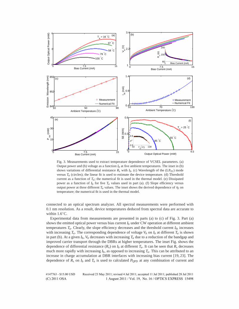
Fig. 3. Measurements used to extract temperature dependence of VCSEL parameters. (a)Output power and (b) voltage as a function Ib at five ambient temperatures. The inset in (b)shows variations of differential resistance Rs with Ib. (c) Wavelength of the (LP01) modeversus Ta (circles); the linear fit is used to estimate the device temperature. (d) Thresholdcurrent as a function of Ta; the numerical fit is used in the thermal model. (e) Dissipatedpower as a function of Ib for five Ta values used in part (a). (f) Slope efficiency versusoutput power at three different Ta values. The inset shows the derived dependence of ηi ontemperature; the numerical fit is used in the thermal model.
connected to an optical spectrum analyzer. All spectral measurements were performed with0.1 nm resolution. As a result, device temperatures deduced from spectral data are accurate towithin 1.6◦C.
Experimental data from measurements are presented in parts (a) to (c) of Fig. 3. Part (a)shows the emitted optical power versus bias current Ib under CW operation at different ambienttemperatures Ta. Clearly, the slope efficiency decreases and the threshold current Ith increaseswith increasing Ta. The corresponding dependence of voltage Vb on Ib at different Ta is shownin part (b). At a given Ib, Vb decreases with increasing Ta due to a reduction of the bandgap andimproved carrier transport through the DBRs at higher temperatures. The inset Fig. shows thedependence of differential resistance (Rs) on Ib at different Ta. It can be seen that Rs decreasesmuch more rapidly with increasing Ib, as opposed to increasing Ta. This can be attributed to anincrease in charge accumulation at DBR interfaces with increasing bias current [19, 23]. Thedependence of Rs on Ib and Ta is used to calculated PQPD at any combination of current and
#147763 - $15.00 USD Received 23 May 2011; revised 4 Jul 2011; accepted 11 Jul 2011; published 28 Jul 2011(C) 2011 OSA 1 August 2011 / Vol. 19, No. 16 / OPTICS EXPRESS 15498

Table 1. Room Temperature Values of VCSEL Parameters
Parameter Value
λ 850.9 ± 0.31 nm
Rth 1.965 ± 0.029◦C mW−1
αi (7.0±0.21)×10−2 ps−1
αTm 5.89×10⁻² ps−1
αBm 6.27×10⁻³ ps−1
Ta. Figure 3(c) shows the emission wavelength of the fundamental LP01 mode at different Ta,measured close to lasing threshold to avoid self-heating. The deduced linear dependence ofwavelength on temperature is subsequently used to find the device temperature at any combi-nation of Ta and Ib under CW operation.
3.3. Extraction of VCSEL Parameters
Plots used for extracting the temperature dependence of various parameters are shown in parts(d) to (f) of Fig. 3. Part (d) shows the dependence of Ith on device temperature, with minimumIth occurring at the temperature for which the gain peak is spectrally aligned with the cavityresonance (30◦C for the device under test) [22]. Here we use a two-segment line-fit to calcu-late threshold current at any ambient temperature from the corresponding Popt–Ib curve. Thismethod is relatively insensitive to changes in slope efficiency [25]. A parabolic numerical fit isused to model the dependence of Ith on Ta. The maximum error in the calculated value of Ith isless than 2% at any Ta. Part (e) shows the dependence of dissipated power, Ptot = IbVb−Popt, onIb at different ambient temperatures. At any bias current, a slight increase in dissipated powerwith increasing Ta is observed. The reason behind this will be discussed in detail in Section5. Part (f) shows the dependence of slope efficiency on output power at different Ta. Follow-ing the procedure outlined in Section 2.2 and using Eqs. (13) and (14), the dependence of theinternal quantum efficiency (ηi) on the device temperature is deduced and plotted in the insetof Fig. 3(f). The ηi is nearly constant and close to 88% at low device temperatures, but it de-creases quite rapidly as the device temperature is increased beyond 50◦C. A polynomial fit isused to represent ηi(T ). The maximum calculated error in the extracted value of ηi is less than1 % at any Ta. To enable the calculation of ηi(T ) from Eq. (14), we use values for the internaloptical loss obtained using the method outlined in [10] and briefly described in Section 2. Theinternal optical loss was found to increase linearly with ambient temperature, from 0.070 ps−1
at 25◦C, to 0.097 ps−1 at 85◦C. This is consistent with the linear dependence of the free-carrierabsorption coefficient on temperature [10].
Tables 1 and 2 list several device parameters whose value was found to vary linearly withtemperature. Table 1 lists the room temperature values, while Table 2 lists the slope of thelinear temperature dependence. These tables also summarize the error in the measured values ofVCSEL parameters. The origin of this error has been discussed in Section 2.2. Since αT
m(T ) andαB
m(T ) are calculated numerically, their values are assumed to be accurate. Physical explanationbehind the temperature dependence as well as previously reported room temperature values forthese parameters can be found in [3, 10, 20, 29].
#147763 - $15.00 USD Received 23 May 2011; revised 4 Jul 2011; accepted 11 Jul 2011; published 28 Jul 2011(C) 2011 OSA 1 August 2011 / Vol. 19, No. 16 / OPTICS EXPRESS 15499

Table 2. Linear Temperature Dependence of VCSEL Parameters (�= ∂∂T )
Parameter Value
�λ (6.07±0.13)×10−2 nm◦C−1
�Rth (5.4±0.4)×10−3 mW−1
�αi (4.167±0.11)×10−4 ps−1◦C−1
�αTm −3.622×10⁻⁵ ps−1◦C−1
�αBm −5.705×10⁻⁶ ps−1◦C−1
0 7.5 150
3
6
Out
put O
ptic
al P
ower
(m
W) (a)
Ta = 25 °C
55 °C
85 °C
0 7.5 150
23
46
P to
t (m
W)
(b)
0 7.5 150
80
160
Bias Current (mA)
Dev
ice
Tem
pera
ture
(° C) (c)
Fig. 4. Comparison of simulated (solid lines) and measured (symbols) values of (a) outputpower, (b) total dissipated power, and (c) device temperature as a function of Ib at threedifferent ambient temperatures [Ta = 25, 55, and 85◦C].
4. Predictions from the Thermal Model
After having deduced the temperature dependence of all VCSEL parameters from the experi-mental data, our empirical thermal model should be able to reproduce measured VCSEL char-acteristics. We use the procedure outlined in Section 2, with the parameters listed in Tables 1and 2 to numerically calculate various contributions to the dissipated power. Parts (a) to (c)of Fig. 4 show the measured and simulated output powers, total dissipated powers, and devicetemperatures as a function of Ib at three ambient temperatures (Ta = 25, 55 and 85◦C). Thetheoretical predictions based on Eqs. (10)–(12) are found to be in good agreement with themeasured data for all values of Ib. This agreement depicts the optical, electrical, and thermalconsistency of our thermal model as well as underlying accuracy of the extracted temperaturedependence of various VCSEL parameters.
#147763 - $15.00 USD Received 23 May 2011; revised 4 Jul 2011; accepted 11 Jul 2011; published 28 Jul 2011(C) 2011 OSA 1 August 2011 / Vol. 19, No. 16 / OPTICS EXPRESS 15500

To understand the reason behind the saturation of output power at high bias currents, we plotin Fig. 5 the evolution of selected VCSEL parameters with bias current at Ta = 25, 55, and85◦C. Part (a) shows variation of ηi with Ib. At 25◦C ambient temperature, ηi is reduced from88% at threshold to 70% at thermal rollover where the device temperature is close to 100◦C asshown in Fig. 4(c). The reduction in ηi becomes more severe at higher ambient temperatures.For example, when Ta = 85◦C, ηi is reduced to less than 50% at thermal rollover. Figure 5(b)shows the evolution of Ith with Ib. As expected, the threshold current increases with bias currentbecause of current-induced self-heating. The inset plots the derivative dIth/dIb as a function ofIb and shows that this derivative becomes so large near thermal rollover that the rate of increaseof Ith is 0.2 times the change in Ib. Ideally, an Ith insensitive to Ib over a wide range of devicetemperatures is desired, from the standpoint of improving the device thermal performance.This can be achieved by optimizing wavelength detuning between the gain-peak and the cavityresonance at which the VCSEL operates [1, 22].
The VCSEL thermal saturation behavior can now be explained as follows: at any Ta, as Ibincreases, the power dissipated within the VCSEL increases [Eq. (10)]. The corresponding in-crease in temperature [Eq. (11)] reduces ηi and increases Ith and αi, which eventually causesthe thermal rollover. To delay the onset of thermal rollover, the rate of increase of T with re-spect to Ib must be reduced. Traditionally, this has been achieved by reducing series resistanceRs [3, 12, 14] and Rth [11, 20]. In this work, however, we focus on identifying and quantify-ing the relative contributions to linear power dissipation (PLPD) in our device with an aim toformulate design strategies to reduce them. For this purpose, we plot the LPD coefficient K in-troduced in Eq. (2). The three curves in Fig. 5(c) show the total K representing the sum of fourindividual contributions at three ambient temperatures [Ta = 25, 55, and 85◦C]. As seen there,K initially decreases with increasing Ib, reaches a minimum value, and then starts increasing asIb approaches the bias current corresponding to thermal rollover. It is this increase of K withcurrent that causes a rapid increase in internal temperature of our VCSEL, which in turn causesthe thermal rollover behavior.
To understand the peculiar behavior of K(Ib), we decompose the LPD coefficient into indi-vidual coefficients for the four constituent LPD mechanisms. We attach a subscript to K andintroduce Kd = Pd/Ib, where d is the subscript label used in Eqs. (3)–(7) that identifies thespecific LPD mechanism in question. Four individual K parameters are calculated from Eqs.(3)–(7) by simply dividing the four equations with Ib. In Fig. 5(d) we plot these individualLPD coefficients as a function of bias current at Ta = 25◦C. The total K is also plotted forcomparison.
The LPD coefficients representing heating due to carrier leakage and thermalization are fairlyconstant over a large range of Ib but the other two change considerably. Consider first heatingdue to the carrier recombination governed by Krec. This parameter is large at low bias currentsand decreases as Ib increases. This can be understood by noting that heating due to spontaneousrecombination is high below laser threshold as most injected carriers recombine spontaneouslyto produce heat. It is reduced near and beyond the laser threshold because of a clamping ofthe carrier density. Consider next heating due to internal optical loss (absorption of photonsproduced by stimulated emission) governed by Kabs. This heating mechanism starts at laserthreshold and its contribution increases with Ib due to an increase in the number of stimulatedphotons generated inside the laser cavity. The net effect of Krec and Kabs is an initial reductionof K(Ib) with increasing Ib around threshold.
The region bounded by the two vertical dotted lines in Fig. 5(d) corresponds to the regionwhere total K takes its relatively low values. In this region, the coefficients representing ther-malization and absorption heating are nearly constant while the coefficients representing spon-taneous recombination and carrier leakage are slowly decreasing and increasing, respectively.
#147763 - $15.00 USD Received 23 May 2011; revised 4 Jul 2011; accepted 11 Jul 2011; published 28 Jul 2011(C) 2011 OSA 1 August 2011 / Vol. 19, No. 16 / OPTICS EXPRESS 15501

0 7.5 150.4
0.65
0.9
η i
(a)T
a = 25 °C
55 °C
85 °C
0 7.5 150.4
1.2
2
I th (
mA
)
0 7.5 150
0.2
Δ I th
/ Δ
I b
(b)
0 7.5 151.3
1.65
2
Bias Current (mA)
K (
W/A
)
(c)
0 7.5 150
1
2
Bias Current (mA)
K (
W/A
)
K
Kabs
Ktherm K
leakK
rec
(d)
Fig. 5. (a) Internal quantum efficiency, (b) threshold current, and (c) LPD coefficient Kversus current at three ambient temperatures. The inset in (b) shows the derivative dIth/dIbas a function of Ib. (d) Dependence of four individual LPD coefficients on current at 25◦C.Total K is also shown for comparison. Vertical dotted lines mark the region where K isrelatively small.
The net effect is a nearly constant K in this region, implying a linear increase of PLPD withcurrent [Eq. (2)]. Beyond the second dotted line, the coefficient representing carrier leakageincreases, causing an increase of K and a corresponding super-linear increase of PLPD with in-creasing bias current. This is due to a rapid reduction of ηi at high bias currents [Fig. 5(a)]corresponding to an internal device temperature increase in excess of 70◦C [Fig. 4(b)]. Further-more, the coefficient representing internal optical loss saturates at the thermal rollover current,which is consistent with the saturation of the photon density in the laser cavity.
This analysis suggests that, for our particular device, carrier leakage and internal optical ab-sorption are the dominant factors among all the contributions to linear power dissipation. It alsosuggests that a rapid reduction of internal quantum efficiency at high bias currents and ambi-ent temperatures, causing a rapid increase in Pleak, is the dominant contributor to the thermalrollover.
5. Thermal Analysis
In this section, we quantify the contributions from all heat sources (linear and quadratic) to thetotal heat load and to the increase of device temperature with current. Figure 6(a) shows theindividual contributions of PLPD and PQPD to Ptot at Ta = 25, 55, and 85◦C. At any Ta, PLPD
exceeds PQPD. This may seem counterintuitive. However, the proportionality constants (Rs andK, respectively) in Eqs. (1) and (2) themselves depend on temperature, and therefore on Ib, asseen in the inset of Figs. 3(b) and 5(c), respectively. Further, with increasing Ta, PQPD is slightlyreduced while PLPD increases progressively at any bias current.
The individual contributions of Pleak, Ptherm, Prec, and Pabs to PLPD as a function of Ib are shownin Fig. 6(b) at Ta = 25, 55, and 85◦C. At a low ambient temperature (25◦C), internal optical loss(optical absorption) and carrier leakage are the two dominant power dissipation mechanisms.
#147763 - $15.00 USD Received 23 May 2011; revised 4 Jul 2011; accepted 11 Jul 2011; published 28 Jul 2011(C) 2011 OSA 1 August 2011 / Vol. 19, No. 16 / OPTICS EXPRESS 15502

0 7.5 150
13
26
QP
D (
mW
)
0
13
26
LPD
(m
W)
(a)T
a = 25 °C
55 °C
85 °C
0 7.5 150
13
LPD
Con
trib
utio
ns (
mW
) (b)Pd,therm
Pd,rec
Pd,abs
Pd,leak
0 7.5 150
20
40
Bias Current (mA)
Δ T
(° C)
Δ Ttherm
Δ Trec
Δ Tleak
Δ Tabs
Δ Tjoule
(c)
Fig. 6. Comparison of the various VCSEL heating mechanisms at three ambient temper-atures. (a) Total LPD and QPD as a function of Ib; (b) dependence of individual LPDcontributions on Ib, and (c) contributions of LPD and QPD mechanisms to the increase indevice temperature as a function Ib.
With increasing Ib, power dissipation due to optical absorption saturates and eventually rollsover, whereas power dissipation due to carrier leakage is enhanced significantly. The rollover ofthe absorption heating is consistent with the rollover of the photon density while the significantincrease of the leakage heating is consistent with the rapid reduction of the internal quantumefficiency at high temperatures. The reduction in ηi also causes a saturation and subsequentrollover of the power dissipation due to carrier thermalization. Finally, the slight increase ofrecombination heating with Ib is consistent with the increase of Ith, and therefore of the carrierdensity in the quantum wells, with increasing Ib. However, its overall contribution is negligibleat any Ta and Ib. This analysis points to carrier leakage (reduction of ηi with increasing devicetemperature) as being the single most dominant contributor to PLPD limiting the VCSEL thermalperformance, especially at high ambient temperatures.
Figure 6(c) displays the contributions to current-induced self-heating as a function of Ib atTa = 25, 55, and 85◦C. At a low Ta of 25◦C, temperature increase due to PQPD (Joule heating)exceeds that due to heating from optical absorption and carrier leakage. However, at high am-bient temperatures (85◦C), increase in device temperature due to carrier leakage exceeds thatdue to other mechanisms. Also, at any Ta, heating due to carrier leakage increases most rapidlyat high bias currents. This again shows that the reduction of internal quantum efficiency withincreasing device temperature sets the ultimate limit for the thermal performance of this device.
Based on the preceding analysis, we draw the following conclusions regarding design mod-ifications for improving thermal performance of VCSELs. First, to delay the onset of carrierleakage, PQPD and Pabs must be minimized. In a conventional VCSEL with current injectionthrough doped DBRs, this involves a trade-off since higher doping levels lead to reduced re-
#147763 - $15.00 USD Received 23 May 2011; revised 4 Jul 2011; accepted 11 Jul 2011; published 28 Jul 2011(C) 2011 OSA 1 August 2011 / Vol. 19, No. 16 / OPTICS EXPRESS 15503

sistance and increased free-carrier absorption [14, 25, 32]. More effective is the use of an intra-cavity contact and a dielectric top DBR [4] as both resistance and optical absorption can bereduced. In addition, it has been shown that reducing the photon lifetime through increasedtransmission through the top DBR can reduce internal optical absorption, thereby delaying ther-mal rollover [8, 21] and improving dynamic performance [10]. Second, the thermal impedanceshould be reduced, thereby reducing the increase of device temperature for a given amountof dissipated power. This involves the use of mounting and packaging techniques for improv-ing thermal management and the use of more novel techniques such as integration of on-chipmetallic heat spreaders [11]. Finally, further improvements are expected with active region de-signs that prevent an excessive increase of carrier leakage at high temperatures. This involvesthe design of quantum wells and barriers as well as the design of the surrounding separateconfinement hetero-structure [3, 10, 31]. It may also involve the use of e.g. carrier blockinglayers [26, 33].
6. Concluding Remarks
In this paper, we have presented a simple, empirical thermal model to study relative roles of var-ious thermal rollover mechanisms inside VCSELs. The parameters required by this model arededuced experimentally through measurements of output power, voltage and emission wave-length as a function of current at different ambient temperatures, The method is quite generaland can potentially be applied to any VCSEL. Specifically, we used the method for analyzingthe thermal performance of an oxide-confined, 850-nm VCSEL designed with a 9-μm inneraperture diameter and optimized for high-speed operation. The model shows that the thermalsaturation behavior is caused by a rapid increase of device temperature with bias current, whichcauses a reduction in the internal quantum efficiency, an increase in the threshold current andincrease in the internal optical loss.
We carried out an in-depth analysis of various thermal rollover mechanisms for this de-vice from the standpoint of understanding the power-saturation behavior. Our approach relatesmacroscopic VCSEL parameters to various thermal rollover mechanisms and makes an accu-rate estimate, both qualitatively and quantitatively, of various power dissipation mechanismsfrom the total power-dissipation in the device. We conclude that, at any bias current and ambi-ent temperature, power dissipation due to carrier leakage, carrier thermalization, spontaneouscarrier recombination and internal optical absorption together exceeds the power dissipatedacross the series resistance (Joule heating). This may seem counterintuitive given the fact thatthe basic dependence of Joule heating on current is quadratic while that of other heat sourcesis linear. However, the constants of proportionality (Rs and K, respectively) depend themselveson the internal device temperature, and change in opposite directions as the bias current is in-creased close to thermal rollover. Still, quadratic power dissipation is a major source of deviceheating, having a significant impact on the thermal performance of the VCSEL.
A careful analysis of the interplay among various thermal rollover mechanisms yields usefulconclusions from the standpoint of improving the device design for improved thermal perfor-mance. Even though carrier leakage sets the ultimate limit for the thermal performance of ourdevice, directly addressing it by only improving the internal quantum efficiency at high tem-perature is less advantageous as opposed to delaying the onset of its reduction. This can beachieved by reducing the series resistance, reducing the internal optical loss and reducing thethermal impedance, which leads to reduction of the rate of increase of device temperature withbias current. Further modifying the active region design for improved internal quantum effi-ciency at high temperatures may lead to a VCSEL design with superior performance in termsof both increased output optical power and speed at elevated temperatures.
#147763 - $15.00 USD Received 23 May 2011; revised 4 Jul 2011; accepted 11 Jul 2011; published 28 Jul 2011(C) 2011 OSA 1 August 2011 / Vol. 19, No. 16 / OPTICS EXPRESS 15504

Acknowledgments
We acknowledge financial support from the Swedish Institute Guest Scholarship, SwedishFoundation for Strategic Research (SSF), the Swedish Research Council (VR), and the Eu-ropean Union through the project VISIT (FP7-224211). The U.S. authors also acknowledgepartial support through the National Science Foundation award ECCS-1041982. P. P. Bavejathanks Erik Haglund and Manish Jain for their useful comments on this work.
#147763 - $15.00 USD Received 23 May 2011; revised 4 Jul 2011; accepted 11 Jul 2011; published 28 Jul 2011(C) 2011 OSA 1 August 2011 / Vol. 19, No. 16 / OPTICS EXPRESS 15505