Challenges in Serial Electrical Interconnects at 5 to 10...
55
IBM Research IEEE SSCS, Denver Section Seminar | Fort Collins, CO March 2007 © 2007 IBM Corporation Challenges in Serial Electrical Interconnects at 5 to 10 Gb/s and Beyond Troy Beukema IBM T. J. Watson Research Center Yorktown Heights, NY
Transcript of Challenges in Serial Electrical Interconnects at 5 to 10...
IBM Research
IEEE SSCS, Denver Section Seminar | Fort Collins, CO March 2007© 2007 IBM Corporation
Challenges in Serial Electrical Interconnects at 5 to 10 Gb/s and Beyond
Troy BeukemaIBM T. J. Watson Research CenterYorktown Heights, NY

2
IBM Research
Challenges in Serial Electrical Interconnects | IEE E SSCS Seminar Fort Collins, CO | March 2007 © 2007 IBM Corporation
� Introduction� I/O Applications in modern system designs
� Electrical Signaling Approaches
� Line Signaling Approaches� Electrical Channel Characteristics
� Line Model
� Line Degradations� I/O core System Design
� SERDES Architectures
� FFE Equalization
� DFE Equalization
� 6-10Gb/s FFE/DFE System architecture� Serial Link Modeling and Simulation
� Link simulation tool
� Eye Diagram BER Analysis
� I/O Core Degradations� Simulation and Measurement Results
� IEEE 802.3ap Informative Channel Link Simulations
� Simulated Performance vs. FFE and DFE Tap Length
� 25Gb/s simulation results� Summary
Outline

3
IBM Research
Challenges in Serial Electrical Interconnects | IEE E SSCS Seminar Fort Collins, CO | March 2007 © 2007 IBM Corporation
Applications for 5Gb/s-10Gb/s+ Electrical I/O
CPUN. BRIDGE GPU/FPU
Protocol RATELegacy shared bus Single-EndedDDR/DDR2/DDR3 33/66/100/133..866MHzPCI 33/66MHzAGP 66(x1)-533 MHz(x8)ATA/SCSI 33/66/100 MB/s
High Rate Serial, point-to-point, Differential Transmission LineHyperTransport 1.6-3.2-4.8Gb/s+CSI 6.4Gb/sFB-DIMM 2.4-4.8-9.6Gb/s+XDR 3.2-8.0Gb/s+
PCI-E 2.5 Gb/s, 5-6Gb/s.INFINIBAND 2Gb/s+SATA (Serial ATA) 1.3-3.0-6Gb/sFCS (Fibre Channel) 1-2-4-8-10-16Gb/sSAS (Serial Attached SCSI) 1.5Gb/s OIF-CEI 6-10Gb/s (to 25Gb/s)802.3ap 10Gb/s
XFP (Optics module) 9-11Gb/s
PROCESSORBOARD/BLADE
MEM
GPU
PCISharedBus
BRIDGE
STORAGE
USB SATA
STORAGE
FCS
CHIP-TO-CHIP ON-BOARD
BRIDGE
BACKPLANE
I/O BOARD,SWITCH/ROUTE
PROCESSORBOARD, BLADE
Ethernet LAN
SONET WAN
I/O BOARD,STORAGELine Card
SATAINFINIBANDFCS SAN
BOARD-TO-BOARD I/O (802.3ap, OIF CEI, HT)
S. BRIDGE
P2PHT/CSI
SHARED
XFP

4
IBM Research
Challenges in Serial Electrical Interconnects | IEE E SSCS Seminar Fort Collins, CO | March 2007 © 2007 IBM Corporation
Electrical Signaling Underpinning Rate BoostLegacy Parallel Shared-Bus Oriented :Single-EndedTransmission-Line Effects lower due to slower rate
T R
T R
LineCharacteristicImpedance :Ro = ~ 50, diff ~100
VTT VTR
Modern Serial Point-to-Point Oriented :Differential, Termination Matched to
impedance controlled Transmission Line
Rates above1Gb/s challenging(advanced systems pushing more)
Problems at higher speeds :CrosstalkGround bounceSwitching NoiseEMI
Large number of lines in busessuch as ATA to a disk
Two lines used, but more thanMakes up for extra line by 2x,4x, 8x Single-ended speed
Problems Addressed :More Crosstalk/Noise ImmunityGround bounce resistantSwitching noise resistantLess noise generatedImpedance matched to lineLess SE swing neededLower EMILess signal lines for disk attach
Ro
Point-to-point high-speed “Lane”3 to 5 to 10 Gb/s in developing standards
Zo = ~100
RT

5
IBM Research
Challenges in Serial Electrical Interconnects | IEE E SSCS Seminar Fort Collins, CO | March 2007 © 2007 IBM Corporation
Line Signaling Methods : 12.5Gb/s on 25” TlineNRZ-FFE3 PAM4/FFE3
Pro : 2x data rate in same BWCon : more complex Tx, Rx slicer,
may need higher drive levelneeds higher SNR for given BERmore sensitive to nonlinearitymore jitter in edge crossover3x higher peak/error threshold
-> 3x more sensitive to xtalk, ISI
Pro : NRZ Common signaling in standardsWhen RxDFE used, almost always
superior performance to 4-levelLow peak/average powerSimple driver/slicer : good for low V
Con : Not good in terms of spectralefficiency (Bit/s/Hz)
-80ps 80ps-50ps 0ps 50ps-500mV
500mV
-400mV
-300mV
-200mV
-100mV
-0.0mV
100mV
200mV
300mV
400mV
500mV
Eye FFE3 12.5Gb/s [THRU,25i] No Xtalk
Time
Sig
nal A
mpl
itude
Vpd
-25
0
-22
-20
-17
-15
-12
-10
-7.5
-5.0
-2.5
0
log1
0(B
ER
)
H(-12) 74.8% (-40.2,37.4)V(-12) 63.4% 105mV
-160ps 160ps-100ps -50ps 0ps 50ps 100ps-500mV
500mV
-400mV
-300mV
-200mV
-100mV
-0.0mV
100mV
200mV
300mV
400mV
500mV
Eye FFE3 12Gb/s [THRU,25i] No Xtalk
Time
Sig
nal A
mpl
itude
Vpd
-25
0
-22
-20
-17
-15
-12
-10
-7.5
-5.0
-2.5
0
log1
0(B
ER
)
H(-12) 43.6% (-21.8,28.1)V(-12) 17.4% 46.4mV
-80ps 80ps-50ps 0ps 50ps-500mV
500mV
-400mV
-300mV
-200mV
-100mV
-0.0mV
100mV
200mV
300mV
400mV
500mV
Eye DFE1T1-5 12.5Gb/s [THRU,25i] No Xtalk
Time
Sig
nal A
mpl
itude
Vpd
-25
0
-22
-20
-17
-15
-12
-10
-7.5
-5.0
-2.5
0
log1
0(B
ER
)
H(-12) 74.8% (-37.4,43.7)V(-12) 67.2% 160mV
NRZ-DFE5BEST!
14dB baud/2 loss9dB baud/2 loss

6
IBM Research
Challenges in Serial Electrical Interconnects | IEE E SSCS Seminar Fort Collins, CO | March 2007 © 2007 IBM Corporation
� Introduction� I/O Applications in modern system designs
� Electrical Signaling Approaches
� Line Signaling Approaches� Electrical Channel Characteristics
� Line Model
� Line Degradations� I/O core System Design
� SERDES Architectures
� FFE Equalization
� DFE Equalization
� 6-10Gb/s FFE/DFE System architecture� Serial Link Modeling and Simulation
� Link simulation tool
� Eye Diagram BER Analysis
� I/O Core Degradations� Simulation and Measurement Results
� IEEE 802.3ap Informative Channel Link Simulations
� Simulated Performance vs. FFE and DFE Tap Length
� 25Gb/s simulation results� Summary
Outline

7
IBM Research
Challenges in Serial Electrical Interconnects | IEE E SSCS Seminar Fort Collins, CO | March 2007 © 2007 IBM Corporation
Backplane Channel ModelIC with High-Speed Serdes I/O
TXIC PKG VIA FANOUT
LINECARD
VIA CONN VIA BACKPLANE
RXICPKGVIAFANIN
LINECARD
VIACONNVIA
Typical Backplane Environment :Line card 3" to 10" from edge connectorTotal of two connectors in linkBackplane line 20" to 30" in length, total line run up to 40" (1m)Plastic or ceramic BGA packageMultiple Lane I/O Buses... 4 to 8 lines wide or moreAsynchronous clocks
CHALLENGE :To accurately model this channel, needhigh-order N ports (20+) whichdescribe through and crosstalk responsesof each link component, including IC, tohigh freq (10-20GHz or BAUD*2 to BAUD*3Need multiple results for each block due to
build variation and temp/humidity/aging variation!17 BLOCKS, 3 VARIATIONS, 17**3 = ~5000 COMBOS
8
IBM Research
Challenges in Serial Electrical Interconnects | IEE E SSCS Seminar Fort Collins, CO | March 2007 © 2007 IBM Corporation
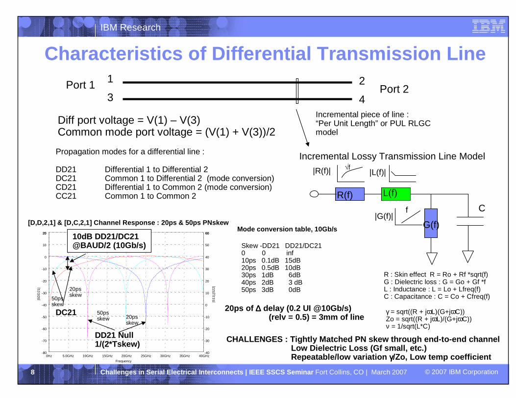
Characteristics of Differential Transmission Line1 2
3 4Port 1 Port 2
Diff port voltage = V(1) – V(3)Common mode port voltage = (V(1) + V(3))/2
R(f) L(f)
G(f)
C
R : Skin effect R = Ro + Rf *sqrt(f)G : Dielectric loss : G = Go + Gf *fL : Inductance : L = Lo + Lfreq(f)C : Capacitance : C = Co + Cfreq(f)
Incremental Lossy Transmission Line Model√f
f
|R(f)| |L(f)|
|G(f)|
Incremental piece of line :“Per Unit Length” or PUL RLGCmodel
0Hz 40GHz5.0GHz 10GHz 15GHz 20GHz 25GHz 30GHz 35GHz-80
20
-70
-60
-50
-40
-30
-20
-10
0
10
20
[D,D,2,1] & [D,C,2,1] Channel Response : 20ps & 50p s PNskew
Frequency
|SD
D21
|
-40
60
-30
-20
-10
0
10
20
30
40
50
60
|S11
|,|S
22|
DD21 Null1/(2*Tskew)
10dB DD21/DC21@BAUD/2 (10Gb/s)
Propagation modes for a differential line :
DD21 Differential 1 to Differential 2DC21 Common 1 to Differential 2 (mode conversion)CD21 Differential 1 to Common 2 (mode conversion)CC21 Common 1 to Common 2
CHALLENGES : Tightly Matched PN skew through end-to -end channelLow Dielectric Loss (Gf small, etc.)Repeatable/low variation γγγγ/Zo, Low temp coefficient
γ = sqrt((R + jωL)(G+jωC))Zo = sqrt((R + jωL)/(G+jωC))ν = 1/sqrt(L*C)
20ps of ∆∆∆∆ delay (0.2 UI @10Gb/s)(relv = 0.5) = 3mm of lineDC21
20psskew
50psskew
50psskew 20ps
skew
Skew -DD21 DD21/DC210 0 inf10ps 0.1dB 15dB20ps 0.5dB 10dB30ps 1dB 6dB40ps 2dB 3 dB50ps 3dB 0dB
Mode conversion table, 10Gb/s
9
IBM Research
Challenges in Serial Electrical Interconnects | IEE E SSCS Seminar Fort Collins, CO | March 2007 © 2007 IBM Corporation
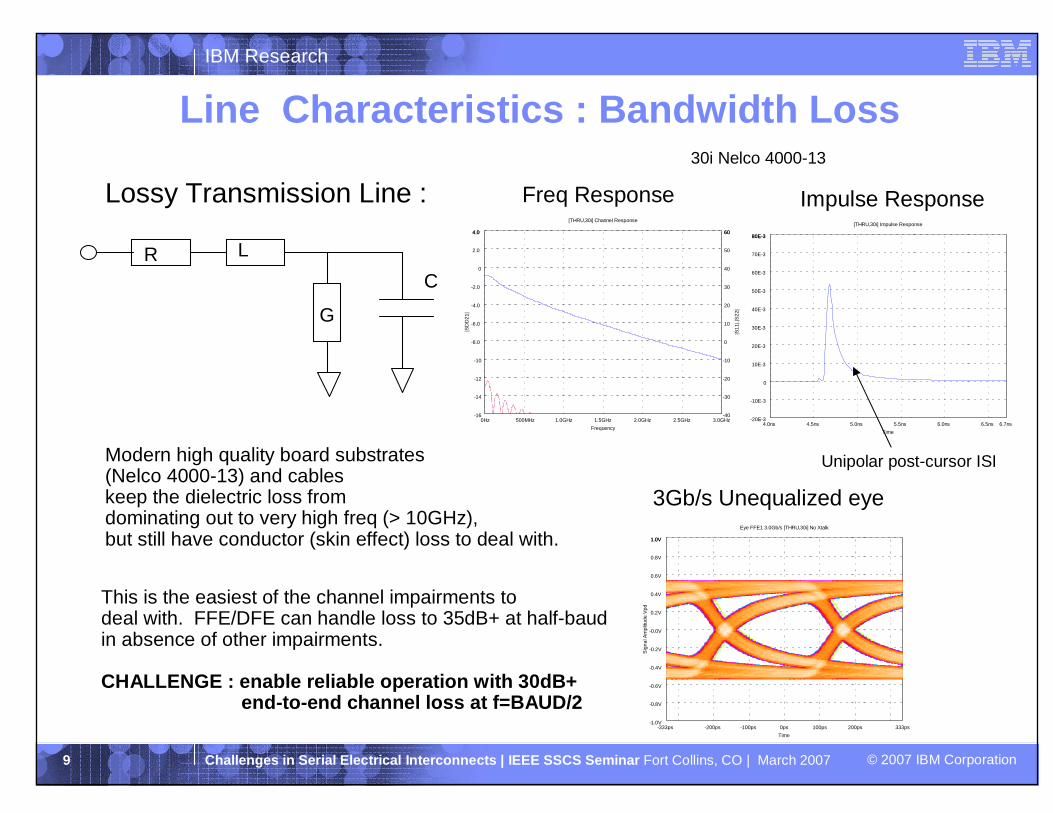
Line Characteristics : Bandwidth Loss
Lossy Transmission Line :
R L
G
C
Modern high quality board substrates(Nelco 4000-13) and cableskeep the dielectric loss fromdominating out to very high freq (> 10GHz),but still have conductor (skin effect) loss to deal with.
This is the easiest of the channel impairments todeal with. FFE/DFE can handle loss to 35dB+ at half-baudin absence of other impairments.
CHALLENGE : enable reliable operation with 30dB+end-to-end channel loss at f=BAUD/2
4.0ns 6.7ns4.5ns 5.0ns 5.5ns 6.0ns 6.5ns-20E-3
80E-3
-10E-3
0
10E-3
20E-3
30E-3
40E-3
50E-3
60E-3
70E-3
80E-3
[THRU,30i] Impulse Response
Time
0Hz 3.0GHz500MHz 1.0GHz 1.5GHz 2.0GHz 2.5GHz-16
4.0
-14
-12
-10
-8.0
-6.0
-4.0
-2.0
0
2.0
4.0
[THRU,30i] Channel Response
Frequency
|SD
D21
|
-40
60
-30
-20
-10
0
10
20
30
40
50
60
|S11
|,|S
22|
30i Nelco 4000-13
Unipolar post-cursor ISI
-333ps 333ps-200ps -100ps 0ps 100ps 200ps-1.0V
1.0V
-0.8V
-0.6V
-0.4V
-0.2V
-0.0V
0.2V
0.4V
0.6V
0.8V
1.0V
Eye FFE1 3.0Gb/s [THRU,30i] No Xtalk
Time
Sig
nal A
mpl
itude
Vpd
Freq Response Impulse Response
3Gb/s Unequalized eye

10
IBM Research
Challenges in Serial Electrical Interconnects | IEE E SSCS Seminar Fort Collins, CO | March 2007 © 2007 IBM Corporation
Reflections from Load Mis-match and Via Stubs
ρ = (Z - Zo)/(Z+Zo)Reflection coefficient :
25
-25
50
-50
100
-100
100250
Zo = 50S11 of load
1pF load
6GHz
0 1|ρ| 0Hz 10GHz2.0GHz 4.0GHz 6.0GHz 8.0GHz-35
15
-30
-25
-20
-15
-10
-5.0
0
5.0
10
15
[THRU,20i] Channel Response
Frequency
|SD
D21
|
-40
60
-30
-20
-10
0
10
20
30
40
50
60
|S11
|,|S
22|
THRU (green/solid) XTALK (dash/black) = NONES11 (green/dash) max(0..BAUD/2) -20.3 dBS22 (green/dot) max(0..BAUD/2) -4.05 dBDC attn = -1.06 dB FC attn = -11.9 dBAv S/Xt = No Xt dB FC S/Xt = No Xt dBPKG = 0/0 TERM = 0/0 IC = 0/0HSSCDR = 2.3.1-4
11.6dB attenuationAt 5GHz
Example 20” T-line at 10.3Gb/swith 1000fF load
Zo
Term :ZC
Zo Zo
Zo
Z = infinity, ρ = 1.0
v v
Adds notch in frequency Domain. Notch goes lowerIn frequency as via stub length (i.e. board thickness)Increases. Results in large level loss at resonance,Signal Time dispersion
25
-25
50
-50
100
-100
100250
r = 1.0Zo = 50S11 of Stub
0Hz 10GHz2.0GHz 4.0GHz 6.0GHz 8.0GHz-45
5.0
-40
-35
-30
-25
-20
-15
-10
-5.0
0
5.0
[THRU,10i] Channel Response
Frequency
|SD
D21
|
-40
60
-30
-20
-10
0
10
20
30
40
50
60
|S11
|,|S
22|
THRU (green/solid) XTALK (dash/black) = NONES11 (green/dash) max(0..BAUD/2) -13.9 dBS22 (green/dot) max(0..BAUD/2) -13.9 dBDC attn = -1.06 dB FC attn = -11.9 dBAv S/Xt = No Xt dB FC S/Xt = No Xt dBPKG = 0/0 TERM = 0/0 IC = 0/0HSSCDR = 2.3.1-4
11.9dB attenuationAt 5GHz
-10dB S11at 2GHz
1) Load Mismatchv
ρv
Results in level loss, setsUp standing waves/reflections
2) Via Stubs
VIA
C = ICPARASITIC
CHALLENGES : LOWER PARASIC LOAD C (T-COIL, ETC.) ELIMINATE VIA STUB (BACKDRILL, ETC.)

11
IBM Research
Challenges in Serial Electrical Interconnects | IEE E SSCS Seminar Fort Collins, CO | March 2007 © 2007 IBM Corporation
Reflections from Non-Homogenous Components
Zo Zo
Term :Zt(f)
ρ= (Z - Zo)/(Z+Zo) =(81-100)/(81+100) = -0.110% signal level gone backup line, loses signal level(most benign reflection)
81 100
1 1-ρ
ρ
PACKAGEBOARD TRACE
Zo Zo100 81
1-ρρ1
PACKAGEBOARD TRACE
ρ2
IC
Multiple Reflections in packageor other link componentsgenerate ISI, not just loss!
ρ3
Typical ∆t = 150ps-> round trip 300ps
IC
package
viavia
BGA VIA/CAP
C4/ESD CAP
CHALLENGES : MINIMIZE COMPONENT IMPEDANCE VARIATIO NSMINIMIZE PARASITICS (BGA cap, etc.)
0s 1.7ns200ps 0.4ns 0.6ns 0.8ns 1.0ns 1.2ns 1.4ns-60E-3
140E-3
-40E-3
-20E-3
0
20E-3
40E-3
60E-3
80E-3
100E-3
120E-3
140E-3
[OPEN,1e-8] Impulse Response
Time

12
IBM Research
Challenges in Serial Electrical Interconnects | IEE E SSCS Seminar Fort Collins, CO | March 2007 © 2007 IBM Corporation
Un-Equalizable ISI from Reflections
FFE DOESN’T EQUALIZE (NOT UNIPOLAR)DFE DOESN’T REACH
Eye Degradations :
1) Large Unequalizable DJ
2) Asymmetric eye, off center
CHALLENGE :Operate in presence of reflections on short,low-loss channels with significant impedancevariation and/or impedance discontinuities.
-333ps 333ps-200ps -100ps 0ps 100ps 200ps-1.0V
1.0V
-0.8V
-0.6V
-0.4V
-0.2V
-0.0V
0.2V
0.4V
0.6V
0.8V
1.0V
Eye FFE1 3.0Gb/s [OPEN,0 No Xtalk
Time
Sig
nal A
mpl
itude
Vpd
Freq Response Impulse Response
3Gb/s Unequalized eye
Unequalizable DJ
2.5ns 12ns4.0ns 5.0ns 6.0ns 7.0ns 8.0ns 9.0ns 10ns 11ns-10E-3
40E-3
-5.0E-3
0
5.0E-3
10E-3
15E-3
20E-3
25E-3
30E-3
35E-3
40E-3
[OPEN,0 Impulse Response
Time0Hz 6.0GHz1.0GHz 2.0GHz 3.0GHz 4.0GHz 5.0GHz
-90
10
-80
-70
-60
-50
-40
-30
-20
-10
0
10
[OPEN,0 Channel Response
Frequency
|SD
D21
|
-40
60
-30
-20
-10
0
10
20
30
40
50
60
|S11
|,|S
22|

13
IBM Research
Challenges in Serial Electrical Interconnects | IEE E SSCS Seminar Fort Collins, CO | March 2007 © 2007 IBM Corporation
Channel Characteristics : Crosstalk
Txdata Rx dataElectrical Channel
TxI/ODevice
data Rx I/ODevice
dataElectrical Channel
Rxdata Tx dataElectrical Channel..
THRU
NE
XT
FEXT
THRU : Through-ChannelNEXT : Near-End CrosstalkFEXT : Far-End Crosstalk
0dB
-20dB
-40dB
FBAUD/2 = 1/(T/2)
20dB attn. @3G closeseye for 1010..
Power Spectrum
NEXT
FEXT
THRU
S/Xt @ BAUD/2 : <10dB = trouble zone
13
24
57
68FEXT
NE
XT9
111012
Two adjacent aggressors captured by 12-port
CHALLENGE :Keep S/Xt > ~10dB at half baud rateon lossy channels.
THRU

14
IBM Research
Challenges in Serial Electrical Interconnects | IEE E SSCS Seminar Fort Collins, CO | March 2007 © 2007 IBM Corporation
Differential Mode Crosstalk Suppression
1
3
2
4
5
7
6
8
Single-ended drive on diff channel = ½ drive on single-ended (SE) for same received signal swing.Therefore closest aggressor couples ½ noise onto nearest victim-> 6dB (2x) inherent crosstalk suppression for diff mode vs. SE
More crosstalk suppression is realized when closest aggressor couplescorrelated signal onto opposite-polarity victim line.-> common-mode crosstalk noise is rejected by differential amplifier
C64 C62
+-V/2
-+V/2Vdiff = V
AGGRESSOR
VICTIM
+
-
+
-
Tx
Rx

15
IBM Research
Challenges in Serial Electrical Interconnects | IEE E SSCS Seminar Fort Collins, CO | March 2007 © 2007 IBM Corporation
Channel Characteristics : Differential Group Delay
Group Delay : τ(ω) = -dφ(ω) / dωH(f) = ρ(ω)ejφ(ω)
Linear System
X Y
High-Freqcrossing
Low-Freqcrossing
Diff Gd = ~ 25ps
-118ps 118ps-50ps 0ps 50ps 100ps-1.0V
1.0V
-0.8V
-0.6V
-0.4V
-0.2V
-0.0V
0.2V
0.4V
0.6V
0.8V
1.0V
Eye FFE1 8.5Gb/s c0_2inch No Xtalk
Time
Sig
nal A
mpl
itude
Vpd
0.4ns 4.8ns1.0ns 1.5ns 2.0ns 2.5ns 3.0ns 3.5ns 4.0ns-15E-3
35E-3
-10E-3
-5.0E-3
0
5.0E-3
10E-3
15E-3
20E-3
25E-3
30E-3
35E-3
c0_2inch Impulse Response
Time
THRU (green/solid)prop delay = 1670 ps imp span = 644 psrms delay = 83.6 ps diff gd = -22.1 psPKG = 0/0 TERM = 0/0 IC = 0/0HSSCDR = 2.3.2 IBM ConfidentialDate = Wed Mar 15 09:15:54 EST 2006
Example xaui 2” test channel
16
IBM Research
Challenges in Serial Electrical Interconnects | IEE E SSCS Seminar Fort Collins, CO | March 2007 © 2007 IBM Corporation
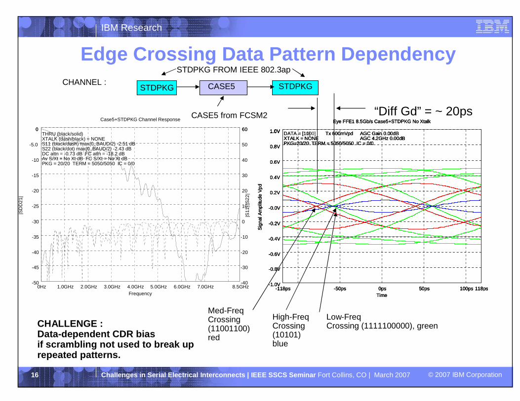
Edge Crossing Data Pattern Dependency
High-FreqCrossing(10101)blue
Low-FreqCrossing (1111100000), green
“Diff Gd” = ~ 20ps
CASE5STDPKG STDPKG
STDPKG FROM IEEE 802.3ap
CHANNEL :
0Hz 8.5GHz1.0GHz 2.0GHz 3.0GHz 4.0GHz 5.0GHz 6.0GHz 7.0GHz-50
0
-45
-40
-35
-30
-25
-20
-15
-10
-5.0
0
Case5+STDPKG Channel Response
Frequency
|SD
D21
|
-40
60
-30
-20
-10
0
10
20
30
40
50
60
|S11
|,|S
22|
THRU (black/solid) XTALK (dash/black) = NONES11 (black/dash) max(0..BAUD/2) -2.51 dBS22 (black/dot) max(0..BAUD/2) -2.43 dBDC attn = -0.73 dB FC attn = -18.2 dBAv S/Xt = No Xt dB FC S/Xt = No Xt dBPKG = 20/20 TERM = 5050/5050 IC = 0/0
-118ps 118ps-50ps 0ps 50ps 100ps-1.0V
1.0V
-0.8V
-0.6V
-0.4V
-0.2V
-0.0V
0.2V
0.4V
0.6V
0.8V
1.0V
Eye FFE1 8.5Gb/s Case5+STDPKG No Xtalk
Time
Sig
nal A
mpl
itude
Vpd
Tx 600mVpd AGC Gain 0.00dBXTALK = NONE AGC 4.2GHz 0.00dBPKG=20/20 TERM = 5050/5050 IC = 0/0
-118ps 118ps-50ps 0ps 50ps 100ps-1.0V
1.0V
-0.8V
-0.6V
-0.4V
-0.2V
-0.0V
0.2V
0.4V
0.6V
0.8V
1.0V
Eye FFE1 8.5Gb/s Case5+STDPKG No Xtalk
Time
Sig
nal A
mpl
itude
Vpd
DATA = [10] Tx 600mVpd AGC Gain 0.00dBXTALK = NONE AGC 4.2GHz 0.00dBPKG=20/20 TERM = 5050/5050 IC = 0/0
-118ps 118ps-50ps 0ps 50ps 100ps-1.0V
1.0V
-0.8V
-0.6V
-0.4V
-0.2V
-0.0V
0.2V
0.4V
0.6V
0.8V
1.0V
Eye FFE1 8.5Gb/s Case5+STDPKG No Xtalk
Time
Sig
nal A
mpl
itude
Vpd
DATA = [1100] Tx 600mVpd AGC Gain 0.00dBXTALK = NONE AGC 4.2GHz 0.00dBPKG=20/20 TERM = 5050/5050 IC = 0/0
Med-FreqCrossing(11001100)red
CASE5 from FCSM2
CHALLENGE :Data-dependent CDR biasif scrambling not used to break uprepeated patterns.

17
IBM Research
Challenges in Serial Electrical Interconnects | IEE E SSCS Seminar Fort Collins, CO | March 2007 © 2007 IBM Corporation
Data Dependency Test Patterns for CDRJTPAT (Jitter Tolerance Pattern)
octet data
The JTPAT octet data generates the following 8/10 encoded bit stream :Low Freq Run length (RL) = 3,4 High Freq Run length (RL) = 11000011100011110001110000….. Followed by 101010101010101010101
CJTPAT (Compliant Jitter Tolerance Pattern)JTPAT payload data in a “compliant” frame format
PROBLEM WITH JTPAT AND CJTPAT :Not enough random data content to excite sufficient ISI patterns afterCDR is biased, can give a false-confidence in eye opening whilethe CDR is biased a large amount. These are not necessarily worst case test patterns.To address this problem a new data dependency stress-test format was defined :
DJTPAT (Data interleaved Jitter Tolerance Pattern : not a standard, defined here) octet data:
This pattern excites 1010, 11001100, and low freq patterns, followed by randomized datato eliminate false confidence in non-random data test patterns (JTPAT/CJTPAT)20 of the above sequences are generated with different random data in each sequence.
High freq (RL 1) Med freq (RL 2) Low freq (RL 3 and 4)
400 0xb5 400 random 400 0x78 400 random 400 0x7e 400 random
400 0x7e 400 0xb5
Data Scrambler breaks up DJTPAT and CJTPAT : Proposed to FCS 8.5Gb, AcceptedRecommend use of data scrambling in ALL high rate s erial links!
18
IBM Research
Challenges in Serial Electrical Interconnects | IEE E SSCS Seminar Fort Collins, CO | March 2007 © 2007 IBM Corporation
� Introduction� I/O Applications in modern system designs
� Electrical Signaling Approaches
� Line Signaling Approaches� Electrical Channel Characteristics
� Line Model
� Line Degradations� I/O core System Design
� SERDES Architectures
� FFE Equalization
� DFE Equalization
� 6-10Gb/s FFE/DFE System architecture� Serial Link Modeling and Simulation
� Link simulation tool
� Eye Diagram BER Analysis
� I/O Core Degradations� Simulation and Measurement Results
� IEEE 802.3ap Informative Channel Link Simulations
� Simulated Performance vs. FFE and DFE Tap Length
� 25Gb/s simulation results� Summary
Outline

19
IBM Research
Challenges in Serial Electrical Interconnects | IEE E SSCS Seminar Fort Collins, CO | March 2007 © 2007 IBM Corporation
Classes of SERDES I/O1) Source Synchronous (forwarded clock) : short, low-loss links (CPU-MEM)
3) Asynchronous (no common reference frequency)
2) Mesochronous (common clock reference frequency)
Phasealign
CLOCK
DATAPRO : TRACKS CLOCK RJ WELL
CON : EXTRA CLOCK LINECLOCK/DATA DESKEW IN
LONG LINENOISE PICKUP ON CLOCKPHASE NOISE FLOOR dBcINCREASE IN LONG LINE
WITH LOSS IN CLK AMP
Phasealign
DATA PRO : GETS RID OF CLOCK LINESTILL SOURCE SYNC
CON : TX/RX BOTH NEED PLLTX/RX NOISE DECORRELATENOISE CORRELATES ONLY IN
PLL BW
PLL PLL
SER
DESERSER
PLL
REF REFREFCLK
SER
PLL
DESER
CDRPLL
DESER
PRO : NO COMMON CLOCKNEEDED AT TX/RX
GOOD FOR LONG LINES
CON : CDR MUST TRACKPHASE AND FREQ BOTH
NO T/R NOISE CORRELATIONCDR MUST TRACK PHASE
NOISE OUT
ParallelData
ParallelData
ParallelData
ParallelData
ParallelData
ParallelDataDATA
REFCLK
REFCLK
REFCLK

20
IBM Research
Challenges in Serial Electrical Interconnects | IEE E SSCS Seminar Fort Collins, CO | March 2007 © 2007 IBM Corporation
Jitter Suppression vs. Clocking Method
Jitter Multiplier SJ term
1.0MHz 3.2GHz = 1/T
500MHz 1.0GHz 1.5GHz 2.0GHz 2.5GHz 0
2.0
0.2
0.4
0.6
0.8
1.0
1.2
1.4
1.6
1.8
2.0
Jitter Multiplier
Jitter Freq
Mul
iplie
r
τ = T
τ = 2T
τ = 3T
ClockingDelay Amplifies Txclock Jitter up to 2x
τ = 0
ASYNC CDR Jitter Suppression
BAUD/1667(tracking bandwidth of PLL)
1.0
Forwarded Clock Jitter Suppression
Jitter Multiplier = 1 – H(f)H(f) = CDR Transfer FunctionPRO : No jitter amplification (if H(f) good)CON : need control loop (PLL) to track jitter
Jitter Multiplier = 2 sin (π * f * τ)τ= delay from clock to data
PRO : Large “automatic” jitter suppression atlow freq with no control loop/PLL
CON : Amplifies jitter 2x in regions, lesssuppression as clock and data get separated
Jitter Freq
Jitte
r M
ultip
lier
1 – H(f)
Peakingpossible at corner dueto loop dynamics

21
IBM Research
Challenges in Serial Electrical Interconnects | IEE E SSCS Seminar Fort Collins, CO | March 2007 © 2007 IBM Corporation
SERDES with Line Equalization
SER
PLL CDRPLL
DESERFFE RXEQ
Transmitter AddsFeed-Forward Equalizerused commonly due to
ease of realization oftapped delay line @ Tx
Receiver Adds Equalizer
Possible Variants :LINEAR (FFE) FIXEDLINEAR (FFE) ADAPTEDDFE FIXEDDFE ADAPTEDLINEAR FIXED DFE ADAPTEDLINEAR ADAPTED DFE ADAPTED
THIS IS A GOOD COMBO. POWERFUL ENOUGHTO BLIND EQUALIZE CHANNEL WITH NOTX FFE IF ENOUGH LINEAR FFE RANGE AVAILABLE
Challenge : maintain low power/area IO Core while g iving high performance line equalization. Power efficiency goals for I/O in range of20-30mW/Gb/s are challenging for 5-10Gb/s rates in 90, 65nm CMOS.
Tx Rx
ParallelData
ParallelData
EqualizersPre-Distortion Post-Compensation

22
IBM Research
Challenges in Serial Electrical Interconnects | IEE E SSCS Seminar Fort Collins, CO | March 2007 © 2007 IBM Corporation
-97ps 97ps-80ps -60ps -40ps -20ps 0ps 20ps 40ps 60ps 80ps-1.0V
1.0V
-0.8V
-0.6V
-0.4V
-0.2V
-0.0V
0.2V
0.4V
0.6V
0.8V
1.0V
Eye TxPkg FFE2 10.3Gb/s [THRU,20i] No Xtalk
Time
Sig
nal A
mpl
itude
Vpd
-25
0
-22
-20
-17
-15
-12
-10
-7.5
-5.0
-2.5
0
log1
0(B
ER
)
H(-12) 99.4% (-49.9,49.7)V(-12) 79.6% 338mV
-97ps 97ps-80ps -60ps -40ps -20ps 0ps 20ps 40ps 60ps 80ps-500mV
500mV
-400mV
-300mV
-200mV
-100mV
-0.0mV
100mV
200mV
300mV
400mV
500mV
Eye FFE2 10.3Gb/s [THRU,20i] No Xtalk
Time
Sig
nal A
mpl
itude
Vpd
-25
0
-22
-20
-17
-15
-12
-10
-7.5
-5.0
-2.5
0
log1
0(B
ER
)
H(-12) 87.2% (-43.6,43.7)V(-12) 68.4% 176mV
-97ps 97ps-80ps -60ps -40ps -20ps 0ps 20ps 40ps 60ps 80ps-1.0V
1.0V
-0.8V
-0.6V
-0.4V
-0.2V
-0.0V
0.2V
0.4V
0.6V
0.8V
1.0V
Eye FFE1 10.3Gb/s [THRU,20i] No Xtalk
Time
Sig
nal A
mpl
itude
Vpd
-25
0
-22
-20
-17
-15
-12
-10
-7.5
-5.0
-2.5
0
log1
0(B
ER
)
H(-12) 56.2% (-28.1,31.0)V(-12) 29.6% 102mV
Feed-Forward EqualizationLinear T-spaced FFE
Un-Equalized Eye Diagram : 50% open
Example 20” T-line at 10.3Gb/s
Eye Diagram with 2-tap FFE : 80% open
Tx FFE effectivelylowers low-frequencywaveform envelopeto level of highfrequency, alsocompensatesgroup delay
~500mvp
Tx Launch Eye with 2-tap FFE
z-1 z-1 Σ channel
Driver
d
Feedforward Equalizer (FFE)
�Problems Addressed by FFE�No feedback settling time problems as in DFE
�Low-power, low area method for line equalization
�Compensates line group delay
�FFE compensates unipolar ISI over wide time span
�Problems with Tx FFE�Lower signal level @ Rx due to
de-emphasis @ Tx
�Decreases SXR (Signal/Crosstalk Ratio)
�Decreases SNR (Signal/Noise Ratio)
�Increases effect of line reflections
�Tx FFE needs a back-channel from Rx
for adaptive equalizer
1010
11,00

23
IBM Research
Challenges in Serial Electrical Interconnects | IEE E SSCS Seminar Fort Collins, CO | March 2007 © 2007 IBM Corporation
-97ps 97ps-80ps -60ps -40ps -20ps 0ps 20ps 40ps 60ps 80ps-1.0V
1.0V
-0.8V
-0.6V
-0.4V
-0.2V
-0.0V
0.2V
0.4V
0.6V
0.8V
1.0V
Eye TxPkg FFE1-5 10.3Gb/s [THRU,20i] No Xtalk
Time
Sig
nal A
mpl
itude
Vpd
-25
0
-22
-20
-17
-15
-12
-10
-7.5
-5.0
-2.5
0
log1
0(B
ER
)
H(-12) 93.6% (-46.8,53.0)V(-12) 90.6% 560mV
-97ps 97ps-80ps -60ps -40ps -20ps 0ps 20ps 40ps 60ps 80ps-1.0V
1.0V
-0.8V
-0.6V
-0.4V
-0.2V
-0.0V
0.2V
0.4V
0.6V
0.8V
1.0V
Eye FFE1 10.3Gb/s [THRU,20i] No Xtalk
Time
Sig
nal A
mpl
itude
Vpd
-25
0
-22
-20
-17
-15
-12
-10
-7.5
-5.0
-2.5
0
log1
0(B
ER
)
H(-12) 56.2% (-28.1,31.0)V(-12) 29.6% 102mV
-97ps 97ps-80ps -60ps -40ps -20ps 0ps 20ps 40ps 60ps 80ps-1.0V
1.0V
-0.8V
-0.6V
-0.4V
-0.2V
-0.0V
0.2V
0.4V
0.6V
0.8V
1.0V
Eye DFE1T1-5 10.3Gb/s [THRU,20i] No Xtalk
TimeS
igna
l Am
plitu
de V
pd
-25
0
-22
-20
-17
-15
-12
-10
-7.5
-5.0
-2.5
0
log1
0(B
ER
)
H(-12) 87.0% (-43.7,43.5)V(-12) 84.0% 256mV
Receiver Equalization : DFE
Σ
h1
z-1 z-1 z-1 z-1 z-1
h2
DFESignal
h3
h4
h5
channel
Nonlinear Equalizer :Feeds back limited estimates of Rx data
Eye Diagram 50% Open
Example 20” T-line channel at 10.3Gb/s
Eye Diagram with 5-tap DFE 87% Open
DFE feedback held constant across 2UI to illustrate ”DFE eye”
Tx Launch Eye with 1-tap FFE
Rx DFE cancels post-cursorISI at the datasampling time withno high-frequencynoise amplificationdue to the non-linearfeedback
�Problems Addressed by DFE�Larger signal @ Rx due to less de-emphasis @ Tx
�Greater SXR
�Greater SNR
�More energy in low-frequency regime where
match is better
�Problems with DFE�Error propagation tendency due to
non-linear feedback
�Need Linear Rx DFE sum
�Increases power draw and area
�Settling time of feedback
�Adaptation algorithm -> adds logic complexity
�Does not compensate pre-cursor ISI
�Only cancels ISI over a fixed time span = DFE lengt h
1010
11,00

24
IBM Research
Challenges in Serial Electrical Interconnects | IEE E SSCS Seminar Fort Collins, CO | March 2007 © 2007 IBM Corporation
Transmitter FFE/ Receiver DFE Equalization
FFE/DFE = Powerful combination…potential to handlelarge line loss, Example 32dB loss channel at 5GHz. 32dB loss at 5GHzImpulse Response
Example 65” T-line at 10.3125Gb/s
DFE Eye Diagram FFE3-DFE562% OpenTx Launch Eye with 3-tap FFE
z-1 z-1 Σ channel
DriverVGA
Σ
tap weightsx0..x2(not adapted)
Decision-Feedback Equalizer (DFE)
D
Feedforward Equalizer (FFE)
D z-1 z-1 z-1 z-1 z-1
h2 h3 h4 h5
FFE-3 DFE-5
h1
FFE compensatesISI > 5 bits distant,Equalizes group delay
DFE enables lessFFE to be used, finetunes channelequalization for 0ISI in range of 1-5bits delayed.
-97ps 97ps-80ps -60ps -40ps -20ps 0ps 20ps 40ps 60ps 80ps-200mV
200mV
-160mV
-120mV
-80mV
-40mV
0.0mV
40mV
80mV
120mV
160mV
200mV
Eye DFE3T1-5 10.3Gb/s [THRU,65i] No Xtalk
Time
Sig
nal A
mpl
itude
Vpd
-25
0
-22
-20
-17
-15
-12
-10
-7.5
-5.0
-2.5
0
log1
0(B
ER
)
H(-12) 62.4% (-31.2,34.1)V(-12) 44.2% 35.2mV
-97ps 97ps-80ps -60ps -40ps -20ps 0ps 20ps 40ps 60ps 80ps-1.0V
1.0V
-0.8V
-0.6V
-0.4V
-0.2V
-0.0V
0.2V
0.4V
0.6V
0.8V
1.0V
Eye TxPkg FFE3-5 10.3Gb/s [THRU,65i] No Xtalk
Time
Sig
nal A
mpl
itude
Vpd
-25
0
-22
-20
-17
-15
-12
-10
-7.5
-5.0
-2.5
0
log1
0(B
ER
)
H(-12) 93.6% (-46.8,46.8)V(-12) 22.8% 82.0mV
4.1ns 18ns6.0ns 8.0ns 10ns 12ns 14ns 16ns 0
5.0E-3
0
0.5E-3
1.0E-3
1.5E-3
2.0E-3
2.5E-3
3.0E-3
3.5E-3
4.0E-3
4.5E-3
5.0E-3
[THRU,65i] Impulse Response
Time
0Hz 10GHz2.0GHz 4.0GHz 6.0GHz 8.0GHz-80
20
-70
-60
-50
-40
-30
-20
-10
0
10
20
[THRU,65i] Channel Response
Frequency
|SD
D21
|
-40
60
-30
-20
-10
0
10
20
30
40
50
60
|S11
|,|S
22|

25
IBM Research
Challenges in Serial Electrical Interconnects | IEE E SSCS Seminar Fort Collins, CO | March 2007 © 2007 IBM Corporation
System Architecture for 6-10Gb/s FFE/DFE 1
z-1 z-1 Σ channel
DriverVGA
Σ
tap weightsx0..x2(not adapted)
Rx Decision-Feedback Equalizer (DFE)
D
Feedforward Equalizer (FFE)
DeFFE-3 DFE-5
Key Transmitter Design Features :o 3 or 4-tap FFE, 1-precursor,1or 2-postcursoro 1200mVppd output nom. 850mVppd output min
o Target S22 >-10dB to 1/2 BAUD freq
Key Receiver Design Features :o VGA to maintain linearity for DFEo Combination of 1/2 rate architecture + speculative 1st-tap feedback with dynamic h2..h5 feedback to enable operation of DFE to 10Gb+o Target S11 >-10dB to 1/2 BAUD freqo Low jitter LC PLL (0.5% UI RMS RJ typ)
Tx and Rx :o Target S21 for minimal loss at 1/2 BAUD freqo Term R from 42 to 58 ohm SE or better, o Clocks <1% RMS RJ (TX+Rx)o Power : 130nm 43mW/Gb/s (6.4G product) 90nm 30mW/Gb/s (10G prototype)
Σ z-1
z-1Σ sel
2:1+h1
-h1
ΣDo
Σ z-1
z-1Σ sel
2:1+h1
-h1
h2..h5
DFE
Σ Σ00
Σ0
z-1
z-1
CDR
PEAK
Σ z-1
h1
LC PLL φ
A
EDynamic h2..h5 feedbackSpeculative h1 feedback
offset
phase
phase rotators
1 Michael Sorna et al. , ISSCC2005, “A 6.4Gb/s CMOS Serdes Core with Feedforward and Decision-Feedback Equalization”Troy Beukema et. al. IEEE J. Solid State Circuits, “A 6.4Gb/s CMOS SerDes Core with FFE and DFE”, December 2005.Mounir Meghelli et. al. ISSCC2006, “A 10Gb/s 5-tap DFE/4-Tap-FFE Transceiver in 90nm CMOS”John Bulzacchelli et. Al. IEEE J. Solid State Circuits, “A 10-Gb/s 5-Tap DFE/4-Tap FFE Transceiver in 90-nm CMOS Technology”, December 2006
Challenges : PVT variations increasing, VDD going d own vs. process : 130nm->90nm->65nm->45nm->30nm->…Keep power and area under control while realizing h igh performance equalizer
26
IBM Research
Challenges in Serial Electrical Interconnects | IEE E SSCS Seminar Fort Collins, CO | March 2007 © 2007 IBM Corporation
� Introduction� I/O Applications in modern system designs
� Electrical Signaling Approaches
� Line Signaling Approaches� Electrical Channel Characteristics
� Line Model
� Line Degradations� I/O core System Design
� SERDES Architectures
� FFE Equalization
� DFE Equalization
� 6-10Gb/s FFE/DFE System architecture� Serial Link Modeling and Simulation
� Link simulation tool
� Eye Diagram BER Analysis
� I/O Core Degradations� Simulation and Measurement Results
� IEEE 802.3ap Informative Channel Link Simulations
� Simulated Performance vs. FFE and DFE Tap Length
� 25Gb/s simulation results� Summary
Outline

27
IBM Research
Challenges in Serial Electrical Interconnects | IEE E SSCS Seminar Fort Collins, CO | March 2007 © 2007 IBM Corporation
Behavioral Link Simulator
-80pS 80pS-50pS 0pS 50pS-500mV
500mV
-400mV
-300mV
-200mV
-100mV
-0.0mV
100mV
200mV
300mV
400mV
500mV
Eye FFE4 12Gb/s Ideal No Xtalk
Time
Sig
nal A
mpl
itude
Vpd
DATA = RANDXTALK = NONE
Tx 600mVpd AGC Gain -5.07dB AGC 6.2GHz -6.56dB
PKG=0/0SJ=1.0e-02cyc/UI 0.05UIpp
DFECDR = 2.0pre1PLL = 1,32pt/UI FREQ OFS = 0.00ppm/0.00usFFE MMSE = [-0.033, 0.765, -0.117, 0.085]
LinkSimulator
S-parametersT-line models
I/O CoreConfiguration
Describe ChannelIncluding packageModels.
Describe I/O CoreIncluding IC models,clock jitter, noise, etc.
-1.0 1.0-500E-3 0 500E-3-25
0
-22
-20
-17
-15
-12
-10
-7.5
-5.0
-2.5
0
BER DFE4T1-5 5.0Gb/s [THRU,3 No Xtalk
Time t (1.0=T)
log1
0(B
ER
)
Eye Diagrams
BER Results
Channel Response
�Inputs
�Link Channel Parameters (Package/IC/Thru/Xtalk responses)
�I/O Core characteristics (CDR & DFE algorithm #FFE/DFE taps, RJ, SJ..)
�Outputs
�Cascaded Channel Responses (Freq, Time, S11, delay, attn, etc.)
�Eye Diagrams
�Bathtub Curves (BER vs. Eye position) and BER floor
�Vertical eye statistics
�PLL statistics, Jitter Tolerance Plots
�FFE tap weights and adapted DFE tap weights
�Features
� Fast concatenation of high order N-ports (15 20 ports, 20 seconds)
� 1Mb/minute typical simulation speed on modern 2GHz SSE laptop0Hz 10GHz2.0GHz 4.0GHz 6.0GHz 8.0GHz
-35
15
-30
-25
-20
-15
-10
-5.0
0
5.0
10
15
[THRU,20i] Channel Response
Frequency
|SD
D21
|
-40
60
-30
-20
-10
0
10
20
30
40
50
60
|S11
|,|S
22|
THRU (green/solid) XTALK (dash/black) = NONES11 (green/dash) max(0..BAUD/2) -20.3 dBS22 (green/dot) max(0..BAUD/2) -4.05 dBDC attn = -1.06 dB FC attn = -11.9 dBAv S/Xt = No Xt dB FC S/Xt = No Xt dBPKG = 0/0 TERM = 0/0 IC = 0/0HSSCDR = 2.3.1-4

28
IBM Research
Challenges in Serial Electrical Interconnects | IEE E SSCS Seminar Fort Collins, CO | March 2007 © 2007 IBM Corporation
System Diagram for Behavioral Link Simulator
S-parameter/Impulse Response/RLGC Models for THRU1..THRUN
FFE Convolve DFE
CDR
τΣEyeHistogram
StatisticalPost-process
BathtubCurve
IC TERM PKG TERMPKG ICTHRU1 THRUN..
Impulseresponse
PKG/TERM/ICS-parameters
IC TERM PKG TERMPKG ICXTALKM
IC TERM PKG TERMPKG ICXTALK1
FFE Convolve
Impulseresponse
Impulseresponse..
EyeDiagram
RJ ANΣ
SJ, Freqoffset
AJAM
AJ = deterministic amplitude noiseAN = Gaussian amplitude noiseAM = minimum latch overdriveSJ = deterministic time jitterRJ = random time jitter
Datasource
Cascaded Channel Model
M crosstalkresponses
N Thru Responses
Discrete-TimeSimulation
Σ

29
IBM Research
Challenges in Serial Electrical Interconnects | IEE E SSCS Seminar Fort Collins, CO | March 2007 © 2007 IBM Corporation
50MHz 6.0GHz1.0GHz 2.0GHz 3.0GHz 4.0GHz 5.0GHz-80
20
-70
-60
-50
-40
-30
-20
-10
0
10
20
TX Cascade Response
Frequency
|SD
D21
|
Solid = CascadeDash = Raw BackplanePower Loss = 1.9e+00 dBRed = worst-case package, Blue = nominal pkg.
Frequency Domain SDD21 Time Domain
5.4nS 9.4nS6.0nS 6.5nS 7.0nS 7.5nS 8.0nS 8.5nS 9.0nS-15E-3
35E-3
-10E-3
-5.0E-3
0
5.0E-3
10E-3
15E-3
20E-3
25E-3
30E-3
35E-3
TX.pkg0 Impulse Response
Time
Solid = CascadeDash = Raw BackplaneSolid = CascadeDash = Raw BackplaneRed = worst-case package, Blue = nominal pkg.
Model end-to-end link including IC/package model (driver out to Rx sample latch in)Link constructed by cascading S-parameters of link sections
Combined Channel Model : S-Parameter Cascade
IDFT

30
IBM Research
Challenges in Serial Electrical Interconnects | IEE E SSCS Seminar Fort Collins, CO | March 2007 © 2007 IBM Corporation
Accurate N-port Link Concatenation
1 2
3 45 6
7 8
PhysicalBackplaneBPThree adjacentChannels
1 : OEM provides :4-port submatrixTHRU : BP[5,6,7,8]4-port submatrix NEXT : BP[2,6,4,8]4-port submatrix FEXT : BP[9,6,11,8]
Individual 4-ports then concatenated :T : TXIC : PKG : THRU : PKG : RXICN1 : TXIC : PKG : NEXT : PKG : RXICF1: TXIC : PKG : FEXT : PKG : THRU
This is NOT ACCURATE since the4-port NEXT/FEXT/THRU are computed assuming all other portsare terminated in 50 ohm, but in real system they will be terminatedin package/IC loads.
PKG
PKG
9 10
11 12PKG
TXIC
TXIC
RXIC
FEXT AGGRESSOR
NEXT AGGRESSOR
VICTIM
1 : Inaccurate 4-port submatrix concatenation :
1 2
3 45 6
7 8
PhysicalBackplaneBPThree adjacentChannels
PKG
9 10
11 12
PKG
TXIC
TXIC
RXIC
FEXT AGGRESSOR
NEXT AGGRESSOR
VICTIM
2 : Accurate N-port matrix concatenation :
TXIC
RXIC
RXIC
2 : OEM PROVIDES :12-port backplane model BP
The following 12-port concatenation is done :
CASC = TXIC : PKG : BP : PKG : RXIC
Individual 4-ports are now taken from CASC :T : CASC[5,6,7,8]N1 : CASC[2,6,4,8]F1 : CASC[9,6,11,8]
This method is accurate . Crosstalk levelsare the most impacted by inaccurate approach.
Implicit 50-ohm termination
Challenge : Accurate N-port measurement/modeling/ex tractionto create IC, PKG, BP N-ports (N=12 to 28) to afrequency of 2x to 3x BAUD rate.
PKGTXIC
TERM50
TERM50
31
IBM Research
Challenges in Serial Electrical Interconnects | IEE E SSCS Seminar Fort Collins, CO | March 2007 © 2007 IBM Corporation
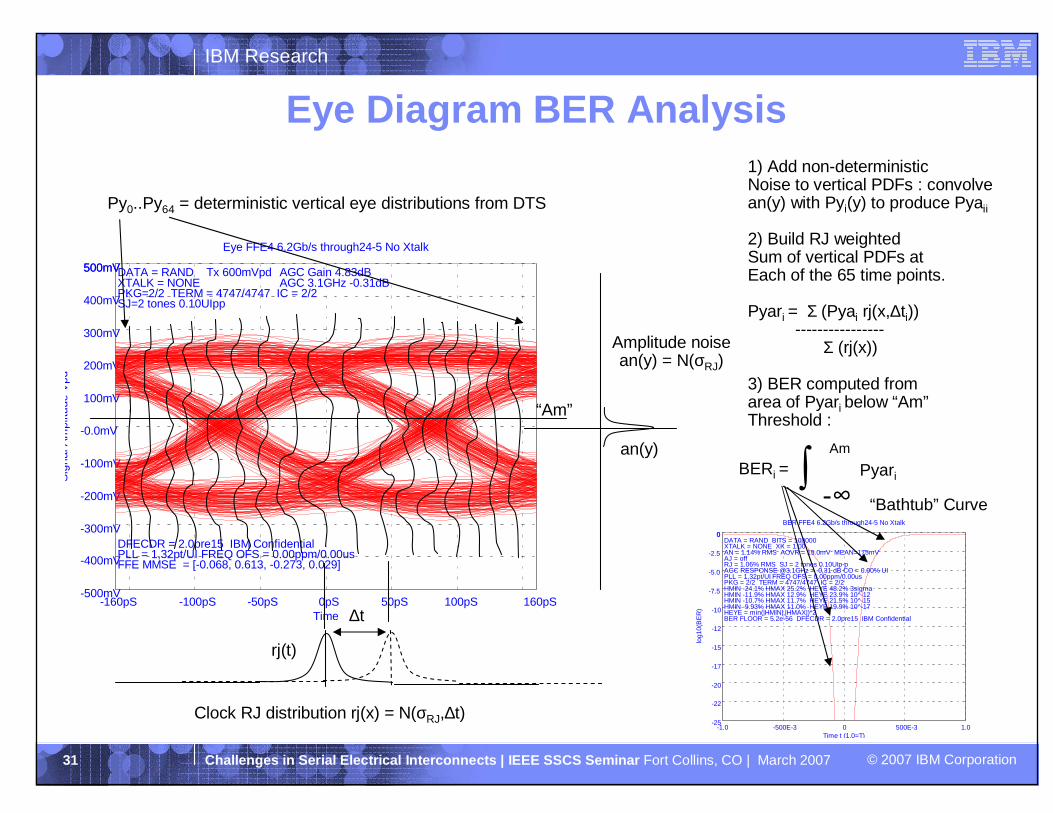
Eye Diagram BER Analysis
-160pS 160pS-100pS -50pS 0pS 50pS 100pS-500mV
500mV
-400mV
-300mV
-200mV
-100mV
-0.0mV
100mV
200mV
300mV
400mV
500mV
Eye FFE4 6.2Gb/s through24-5 No Xtalk
Time
Sig
nal A
mpl
itude
Vpd
DATA = RANDXTALK = NONE
Tx 600mVpd AGC Gain 4.83dBAGC 3.1GHz -0.31dB
PKG=2/2 TERM = 4747/4747 IC = 2/2SJ=2 tones 0.10UIpp
DFECDR = 2.0pre15 IBM ConfidentialPLL = 1,32pt/UI FREQ OFS = 0.00ppm/0.00usFFE MMSE = [-0.068, 0.613, -0.273, 0.029]
Py0..Py64 = deterministic vertical eye distributions from DTS
“Am”
Clock RJ distribution rj(x) = N(σRJ,∆t)
Amplitude noisean(y) = N(σRJ)
an(y)
rj(t)
1) Add non-deterministicNoise to vertical PDFs : convolvean(y) with Pyi(y) to produce Pyaii
2) Build RJ weightedSum of vertical PDFs atEach of the 65 time points.
Pyari = Σ (Pyai rj(x,∆ti))----------------
Σ (rj(x))
3) BER computed fromarea of Pyari below “Am”Threshold :
∫
∆t
-∞
Am
Pyari
-1.0 1.0-500E-3 0 500E-3-25
0
-22
-20
-17
-15
-12
-10
-7.5
-5.0
-2.5
0
BER FFE4 6.2Gb/s through24-5 No Xtalk
Time t (1.0=T)
log1
0(B
ER
)
DATA = RAND BITS = 100000XTALK = NONE XK = 1.00AN = 1.14% RMS AOVR = 15.0mV MEAN=175mVAJ = offRJ = 1.06% RMS SJ = 2 tones 0.10UIp-pAGC RESPONSE @3.1GHz = -0.31 dB CO = 0.00% UIPLL = 1,32pt/UI FREQ OFS = 0.00ppm/0.00usPKG = 2/2 TERM = 4747/4747 IC = 2/2HMIN -24.1% HMAX 25.2% HEYE 48.2% 3sigmaHMIN -11.9% HMAX 12.9% HEYE 23.9% 10^-12HMIN -10.7% HMAX 11.7% HEYE 21.5% 10^-15HMIN -9.93% HMAX 11.0% HEYE 19.9% 10^-17HEYE = min(|HMIN|,|HMAX|)*2BER FLOOR = 5.2e-56 DFECDR = 2.0pre15 IBM Confidential
BERi =
“Bathtub” Curve

32
IBM Research
Challenges in Serial Electrical Interconnects | IEE E SSCS Seminar Fort Collins, CO | March 2007 © 2007 IBM Corporation
�Clock Jitter
�Random Jitter (RJ) from VCO phase noise
�Sinusoidal Jitter (SJ) from power supply clock tree s etc.
�Deterministic Jitter (DJ) from IC/package/channel
�Duty Cycle Distortion (DCD) at Transmit Launch
�Amplitude Noise
�Non-Deterministic Amplitude Noise (AN) (thermal/kT noise)
�Deterministic Amplitude noise (AJ) : power-supply, switching noise
�Crosstalk : In IC substrate/package (as opposed to line alone)
�Minimum-Latch Overdrive (AM)
�Important for small signal swing/low V systems
I/O Core Related Link Degradations

33
IBM Research
Challenges in Serial Electrical Interconnects | IEE E SSCS Seminar Fort Collins, CO | March 2007 © 2007 IBM Corporation
Gaussian Noise Modulates Clock Phase
7σ
1UI
p(t)~1e-12
Clock edge jitters+-7σ at 1e-12 prob.
Eye closedRJ=50%UI /7= 7% UI RMS
0.5UI
Time Axis
p(t) = clock jitter PDF
Eye closure = 14*RJ7% RMS RJBER floor ~ 1E-12
Random Jitter (RJ) Distortion
CHALLENGE : KEEP TOTAL RJ FROM TX/RX < 1% RMS-160ps 160ps-100ps -50ps 0ps 50ps 100ps
-1.0V
1.0V
-0.8V
-0.6V
-0.4V
-0.2V
-0.0V
0.2V
0.4V
0.6V
0.8V
1.0V
Eye FFE1 6.3Gb/s [THRU,1i] No Xtalk
Time
Sig
nal A
mpl
itude
Vpd
-25
0
-22
-20
-17
-15
-12
-10
-7.5
-5.0
-2.5
0
log1
0(B
ER
)
H(-12) 0.08% (-0.04,0.04)V(-12) 3.00% 17.5mV
-160ps 160ps-100ps -50ps 0ps 50ps 100ps-1.0V
1.0V
-0.8V
-0.6V
-0.4V
-0.2V
-0.0V
0.2V
0.4V
0.6V
0.8V
1.0V
Eye FFE1 6.3Gb/s [THRU,1i] No Xtalk
Time
Sig
nal A
mpl
itude
Vpd
-25
0
-22
-20
-17
-15
-12
-10
-7.5
-5.0
-2.5
0
log1
0(B
ER
)
H(-12) 43.6% (-25.0,21.8)V(-12) 60.6% 352mV
Simulated RJ
Statistical RJ

34
IBM Research
Challenges in Serial Electrical Interconnects | IEE E SSCS Seminar Fort Collins, CO | March 2007 © 2007 IBM Corporation
RJ Computation from PLL Phase Noise
L(f)(dBc/Hz)=(rad2/Hz)
f = Freq Offset from CarrierF1pll tracking BW
1/f**2 (in power)region
noise floor
Fc= 1/T
Phase Noise Power Spectrum Multiplier for FW clock (2sin(π*f*τ))VCO Phase Noise Density function L(f)
RMS Jitter (τ) =
0
~Fc/2
2 S(f) * L(f) df1
2πFc
Phase Noise Multiplier :Async CDR : S(f) = 1 - H(f)Ssync CDR : S(f) = (2 * sin(π*f*τ))
F2
L1
L2
2
2
Phase Noise Power Spectrum Multiplier for Async CDR (1-H(f))2
1.0
2.0

35
IBM Research
Challenges in Serial Electrical Interconnects | IEE E SSCS Seminar Fort Collins, CO | March 2007 © 2007 IBM Corporation
Sine Wave Modulates Clock Phase
1UI
Clock moveswith SJ
Eye closedSJ=100% UI P-Pif SJ_freq outsidePLL loop BW
"SJ_lev" UI p-p
"SJ_freq"Cycles/UI
Time Axis
Sinusoidal Jitter (SJ) Distortion
-160ps 160ps-100ps -50ps 0ps 50ps 100ps-1.0V
1.0V
-0.8V
-0.6V
-0.4V
-0.2V
-0.0V
0.2V
0.4V
0.6V
0.8V
1.0V
Eye FFE1 6.3Gb/s [THRU,1i] No Xtalk
Time
Sig
nal A
mpl
itude
Vpd
-25
0
-22
-20
-17
-15
-12
-10
-7.5
-5.0
-2.5
0
log1
0(B
ER
)
H(-12) 49.8% (-28.0,24.9)V(-12) 92.0% 543mV
-160ps 160ps-100ps -50ps 0ps 50ps 100ps-1.0V
1.0V
-0.8V
-0.6V
-0.4V
-0.2V
-0.0V
0.2V
0.4V
0.6V
0.8V
1.0V
Eye FFE1 6.3Gb/s [THRU,1i] No Xtalk
Time
Sig
nal A
mpl
itude
Vpd
-25
0
-22
-20
-17
-15
-12
-10
-7.5
-5.0
-2.5
0
log1
0(B
ER
)
H(-12) 49.8% (-28.1,24.9)V(-12) 92.2% 544mV
5 SJ TONES EACH 10% UI PP
1 SJ TONE 50% UI PP
Challenge : Minimize Effect of Supply Noise to mini mize SJcomponent of clock
36
IBM Research
Challenges in Serial Electrical Interconnects | IEE E SSCS Seminar Fort Collins, CO | March 2007 © 2007 IBM Corporation
-160ps 160ps-100ps -50ps 0ps 50ps 100ps-1.0V
1.0V
-0.8V
-0.6V
-0.4V
-0.2V
-0.0V
0.2V
0.4V
0.6V
0.8V
1.0V
Eye FFE1 6.3Gb/s [THRU,1i] No Xtalk
Time
Sig
nal A
mpl
itude
Vpd
-25
0
-22
-20
-17
-15
-12
-10
-7.5
-5.0
-2.5
0
log1
0(B
ER
)
H(-12) 7.97% (-3.98,7.16)V(-12) 2.74% 15.9mV
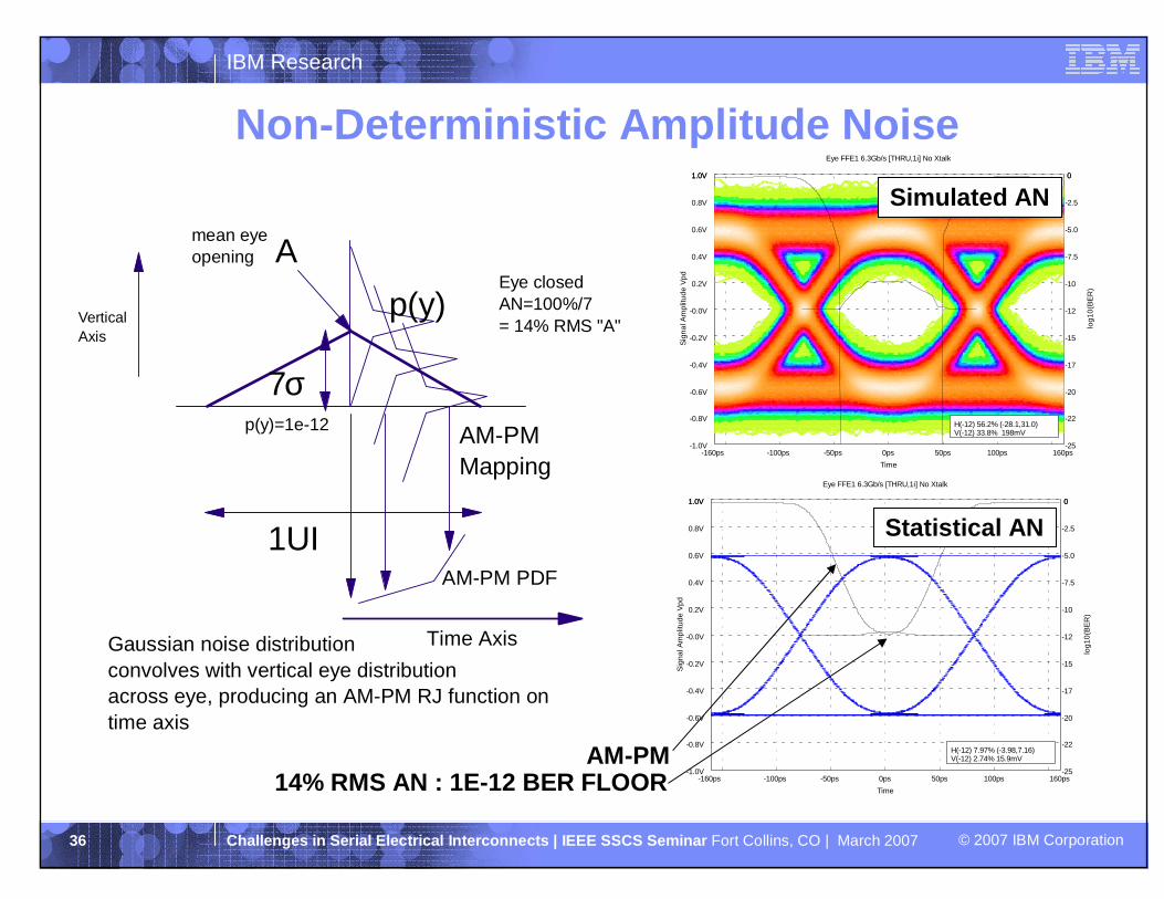
p(y)
Amean eyeopening
AM-PM PDF
1UI
7σp(y)=1e-12 AM-PM
Mapping
Gaussian noise distributionconvolves with vertical eye distributionacross eye, producing an AM-PM RJ function ontime axis
Eye closedAN=100%/7= 14% RMS "A"
Time Axis
VerticalAxis
Non-Deterministic Amplitude Noise
AM-PM14% RMS AN : 1E-12 BER FLOOR
-160ps 160ps-100ps -50ps 0ps 50ps 100ps-1.0V
1.0V
-0.8V
-0.6V
-0.4V
-0.2V
-0.0V
0.2V
0.4V
0.6V
0.8V
1.0V
Eye FFE1 6.3Gb/s [THRU,1i] No Xtalk
Time
Sig
nal A
mpl
itude
Vpd
-25
0
-22
-20
-17
-15
-12
-10
-7.5
-5.0
-2.5
0
log1
0(B
ER
)
H(-12) 56.2% (-28.1,31.0)V(-12) 33.8% 198mV
Simulated AN
Statistical AN

37
IBM Research
Challenges in Serial Electrical Interconnects | IEE E SSCS Seminar Fort Collins, CO | March 2007 © 2007 IBM Corporation
Tx Duty Cycle Distortion
Short pulse duration Ts
Long pulse duraton TlDuty cycle distortion
Lossy Channel
Duty-cycle distortion amplified at Rx
More DJ at Rx from jitter amplification in channel
DCD = Ts/(Ts+Tl)Example :
48:52 DCD, short pulse = 48 units mean UI 50 units-> 4% UIpp DCD shutdown in low-loss channelcan result in 8% or more shutdown in lossy channel
Signal with Duty Cycle Distortion
-160ps 160ps-100ps -50ps 0ps 50ps 100ps-200mV
200mV
-160mV
-120mV
-80mV
-40mV
0.0mV
40mV
80mV
120mV
160mV
200mV
Eye FFE2 6.3Gb/s [THRU,60i] No Xtalk
Time
Sig
nal A
mpl
itude
Vpd
-25
0
-22
-20
-17
-15
-12
-10
-7.5
-5.0
-2.5
0
log1
0(B
ER
)
H(-12) 56.2% (-29.7,28.1)V(-12) 27.8% 28.2mV
-160ps 160ps-100ps -50ps 0ps 50ps 100ps-200mV
200mV
-160mV
-120mV
-80mV
-40mV
0.0mV
40mV
80mV
120mV
160mV
200mV
Eye FFE2 6.3Gb/s [THRU,60i] No Xtalk
Time
Sig
nal A
mpl
itude
Vpd
-25
0
-22
-20
-17
-15
-12
-10
-7.5
-5.0
-2.5
0
log1
0(B
ER
)
H(-12) 42.7% (-24.9,21.3)V(-12) 17.6% 18.1mV
No DCD :Eye 56% Open
6.25% UIpp DCD :Eye 42% Open
CHALLENGE : REALIZE STRINGENT 3% UIpp DCD AT TRANSMI TTER
38
IBM Research
Challenges in Serial Electrical Interconnects | IEE E SSCS Seminar Fort Collins, CO | March 2007 © 2007 IBM Corporation
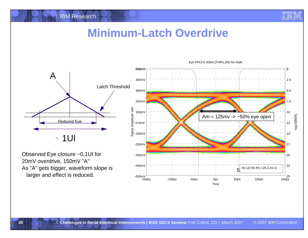
Minimum-Latch Overdrive
A
1UI
Latch Threshold
Reduced Eye
Observed Eye closure ~0.1UI for20mV overdrive, 150mV "A"As "A" gets bigger, waveform slope is larger and effect is reduced.
59% -> ~95ps open
-160ps 160ps-100ps -50ps 0ps 50ps 100ps-500mV
500mV
-400mV
-300mV
-200mV
-100mV
-0.0mV
100mV
200mV
300mV
400mV
500mV
Eye FFE3 6.3Gb/s [THRU,30i] No Xtalk
Time
Sig
nal A
mpl
itude
Vpd
-25
0
-22
-20
-17
-15
-12
-10
-7.5
-5.0
-2.5
0
log1
0(B
ER
)
H(-12) 50.4% (-25.2,34.1)
Am = 125mv -> ~50% eye open

39
IBM Research
Challenges in Serial Electrical Interconnects | IEE E SSCS Seminar Fort Collins, CO | March 2007 © 2007 IBM Corporation
� Introduction� I/O Applications in modern system designs
� Electrical Signaling Approaches
� Line Signaling Approaches� Electrical Channel Characteristics
� Line Model
� Line Degradations� I/O core System Design
� SERDES Architectures
� FFE Equalization
� DFE Equalization
� 6-10Gb/s FFE/DFE System architecture� Serial Link Modeling and Simulation
� Link simulation tool
� Eye Diagram BER Analysis
� I/O Core Degradations� Simulation and Measurement Results
� IEEE 802.3ap Informative Channel Link Simulations
� Simulated Performance vs. FFE and DFE Tap Length
� 25Gb/s simulation results� Summary
Outline

40
IBM Research
Challenges in Serial Electrical Interconnects | IEE E SSCS Seminar Fort Collins, CO | March 2007 © 2007 IBM Corporation
Key I/O Core Parameters for simulation
Tx : Example I/O configuration for a transmitter Rx : Example I/O configuration for a receiver400mVpd minDrive Level
-10dB @ Baud/2S22
40-60TERM
15% p-p UI @1e-12DJ1
1.07% RMS uiRJ
Assumed to include pkg, ESD, IC, DCD
1.4mV RMS input ref.AN
-10dB @ Baud/2S11
40-60TERM
10% p-p UI @1e-12DJ
1.07% RMS uiRJ
15mVAM2
channel
IC IC
ΣD D z-1
h
FFE TERM PKG
PLL
DFEPKG TERM
PLL/CDR
#tapstap weights
drivelevel
termaccuracy
Tx RJ, SJ Tx DJ Rx DJ
termaccuracy
#tapstap weights adaptedLatch Sensitivity (AM)
Σσ2N ∗
Amp.Noise(AN)
Rx RJ, SJ
Tx Rx sgn(D) * AM+-
S22
S11
OutputReflection
InputReflection

41
IBM Research
Challenges in Serial Electrical Interconnects | IEE E SSCS Seminar Fort Collins, CO | March 2007 © 2007 IBM Corporation
Baud/2 Loss and S/Xt for 802.3ap Test Channels 1
802.3ap Test Channel Nyquist Attenuation and Crosstalk Level
0
5
10
15
20
25
30
b1 b12
b20
m1
m20 t1 t1
2
t20
in2
in3
in4
in5
out2
out3
out4
out5
case
1
case
2
case
3
case
4
case
5
case
6
case
7
Intel Molex Tyco
Leve
l (dB
)
Fc Attn
Fc S/Xt
As Fc attenuation increases, S/Xt decreases
1http://grouper.ieee.org/groups/802/3/ap/public/channel_model“Channels for consideration by the signaling ad-hoc”, John D’Ambrosia, Tyco“Improved HVM ATCA Measurement Data”, William Peters, Intel“1m Test vehicle (FR408)”, Gourgen Oganessyan, Molex
12Tyco case6
22Tyco
43Molex
62Intel
#NEXT#FEXTChannels
Crosstalk channels
13.9013.6322.105.69Fc S/Xt
22.6020.2528.109.30Fc Attn
MedianMeanMaxMin

42
IBM Research
Challenges in Serial Electrical Interconnects | IEE E SSCS Seminar Fort Collins, CO | March 2007 © 2007 IBM Corporation
FFE3/DFE5 Equalization, No Pkg or I/O Jitter/Noise 1
Use ideal I/O core, no package to determine maximum possible eye margin with FFE3/DFE5
FFE3/DFE5 Equalization of 802.3ap Channels with Ide al I/O
0102030405060708090
100
b1 b12
b20
m1
m20 t1 t12
t20
in2
in3
in4
in5
out2
out3
out4
out5
case
1
case
2
case
3
case
4
case
5
case
6
case
7
Intel Molex Tyco
Hey
e 1E
-15
(%)
No Pkg No Xt
No Pkg +Xt
13.6015.5612.2016.60Xt H loss
72.4066.5876.6028.60VEYE no Xt
50.2045.9965.6012.80VEYE with Xt
68.6066.1980.8034.80HEYE no Xt
22.2020.5911.0015.80Xt V loss
55.0050.6368.6018.20HEYE with Xt
MedianMeanMaxMin
400mVpdTx Lev
50Tx TERM
NoneTx Pkg
NoneTx IC
0% UIp-pTx DJ
0% RMS UITx RJ 0% RMS UIRx RJ
0% UIp-p SJRx DJ
50Rx TERM
NoneRx Pkg
0mVRx Am
NoneRx IC
0mV RMSRx An
ONRx CDR
1Async CDR running in all simulations
Eye Opening in %
50% UI UEQUALIZABLE DJ80% UI UEQUALIZABLE DJ
43
IBM Research
Challenges in Serial Electrical Interconnects | IEE E SSCS Seminar Fort Collins, CO | March 2007 © 2007 IBM Corporation
FFE3/DFE5 Equalization with Package, no I/O Jitter/N oiseUse ideal I/O core, 3 package models to determine maximum possible eye margin with FFE3/DFE5
FFE3/DFE5 Equalization of 802.3ap Channels with Ide al I/O + Package Model
0102030405060708090
100
b1 b12
b20
m1
m20 t1 t12
t20
in2
in3
in4
in5
out2
out3
out4
out5
case
1
case
2
case
3
case
4
case
5
case
6
case
7
Intel Molex Tyco
Hey
e 1E
-15
(%)
No pkg + Xt
Ind pkg + xt
Cap pkg + xt
STD pkg + xt
17.6013.9413.0012.79LOSS S Pkg
37.4036.6955.605.41HEYE S Pkg
5.606.350.0018.20LOSS C Pkg
5.203.246.2014.25LOSS L Pkg
13.6015.5612.2016.60LOSS Xt
49.8047.3962.403.95HEYE L Pkg
49.4044.2868.600.00HEYE C Pkg
55.0050.6368.6018.20HEYE no Pkg
MedianMeanMaxMin
14.4012.8714.2011.40LOSS S Pkg
35.8033.1251.401.40VEYE S Pkg
4.804.73-4.206.20LOSS C Pkg
3.403.706.8012.00LOSS L Pkg
22.2020.5911.0015.80LOSS Xt
46.8042.2958.800.80VEYE L Pkg
45.4041.2669.806.60VEYE C Pkg
50.2045.9965.6012.80VEYE no Pkg
MedianMeanMaxMin
Horizontal Eye Opening in %Vertical Eye Opening in %
~50% UI UEQUALIZABLE DJ>90% UI UEQUALIZABLE DJ

44
IBM Research
Challenges in Serial Electrical Interconnects | IEE E SSCS Seminar Fort Collins, CO | March 2007 © 2007 IBM Corporation
Example I/O Jitter/Noise Impact to Clean Channel
Eye Opening at 1E-12 vs. added I/O Jitter/Noise
50Tx TERM
NoneTx Pkg
NoneTx IC
5% UIp-p SJTx DJ
1.07% RMS UITx RJ
400mVpdTx Lev
1.4mV RMSRx An
50Rx TERM
NoneRx Pkg
5% UIp-p SJRx DJ
NoneRx IC
1.07% RMS UIRx RJ
15mVRx Am
ONRx CDR
-1.0 1.0-500E-3 0 500E-3-25
0
-22
-20
-17
-15
-12
-10
-7.5
-5.0
-2.5
0
BER FFE2 10.3Gb/s [THRU,8i] No Xtalk
Time t (1.0=T)
log1
0(B
ER
)
RJ alone : 71%
AN alone : 87%
AN + RJ : 68%
AN + RJ + AM + SJ : 42%
AN + RJ + AM : 52% (Rx Gain 1)
Ideal Channel : 100%
AN + RJ + AM + SJ + CDR : 38%
-97ps 97ps-80ps -60ps -40ps -20ps 0ps 20ps 40ps 60ps 80ps-100mV
100mV
-80mV
-60mV
-40mV
-20mV
0.0mV
20mV
40mV
60mV
80mV
100mV
Eye FFE2 10.3Gb/s [THRU,8i] No Xtalk
Time
Sig
nal A
mpl
itud
e V
pd
DATA = RAND Tx 90.0mVpd AGC Gain 0.00dBXTALK = NONE Slew 60.0ps AGC 5.2GHz 0.00dBPKG=0/0 TERM = 0/0 IC = 0/0
FREQ=0.00ppm/0.00usFFE = [0.901, -0.099]

45
IBM Research
Challenges in Serial Electrical Interconnects | IEE E SSCS Seminar Fort Collins, CO | March 2007 © 2007 IBM Corporation
FFE3/DFE5 Equalization with Package and I/O Jitter/N oise
400mVpdTx Lev
40Tx TERM
Cap-likeTx Pkg
NoneTx IC
5% SJ + PkgTx DJ
1.07% RMS UITx RJ
ONRx CDR
15mVRx Am
60Rx TERM
Cap-LikeRx Pkg
5% SJ + PkgRx DJ
NoneRx IC
1.07% RMS UIRx RJ
1.4mV RMSRx An
6.816.6117.000.00LOSS S Pkg
0.001.8512.800.00HEYE S Pkg
5.313.3610.600.00LOSS C Pkg
2.622.185.700.00LOSS L Pkg
16.3912.305.800.00LOSS Xt
4.196.2824.100.00HEYE L Pkg
1.505.1019.200.00HEYE C Pkg
6.818.4629.800.00HEYE no Pkg
MedianMeanMaxMin
FFE3/DFE5 Equalization of 802.3ap Channels with I/O Jitter/Noise + Package
0102030405060708090
100b1 b12
b20
m1
m20 t1 t12
t20
in2
in3
in4
in5
out2
out3
out4
out5
case
1
case
2
case
3
case
4
case
5
case
6
case
7
Intel Molex Tyco
Hey
e 1E
-15
(%)
No pkg + Xt
Ind pkg + xt
Cap pkg + xt
STD pkg + xt
Marginal to OK (>0.15UI)
UnreliableNo operation
Horizontal Eye Opening in %
46
IBM Research
Challenges in Serial Electrical Interconnects | IEE E SSCS Seminar Fort Collins, CO | March 2007 © 2007 IBM Corporation
FFE3/DFE5 802.3ap Channels 900mV Tx, 50:50 TERM, 0 .6% Tx & Rx RJ, Pkg
0102030405060708090
100b1 b12
b20
m1
m20 t1 t12
t20
in2
in3
in4
in5
out2
out3
out4
out5
case
1
case
2
case
3
case
4
case
5
case
6
case
7
Intel Molex Tyco
Hey
e 1E
-15
(%)
No pkg + Xt
Ind pkg + xt
Cap pkg + xt
STD pkg + xt
FFE3/DFE5 Equalization with Reduced Jitter I/O 1
50Tx TERM
VariedTx Pkg
NoneTx IC
5% SJ + PkgTx DJ
0.6% RMS UITx RJ
450mVpdTx Lev
0.6% RMS UIRx RJ
ONRx CDR
50Rx TERM
VariedRx Pkg
5% SJ + PkgRx DJ
NoneRx IC
15mVRx Am
0.7mV RMS inputRefRx An
13.5410.9010.100.00LOSS S Pkg
5.368.3029.100.00HEYE S Pkg
5.105.801.200.00LOSS C Pkg
3.152.730.000.00LOSS L Pkg
23.0517.4610.300.88LOSS Xt
15.7516.4739.200.00HEYE L Pkg
13.8013.4038.000.00HEYE C Pkg
18.9019.2039.200.00HEYE no Pkg
MedianMeanMaxMin1Clock noise 5dB cleanerAmplitude noise ½ levelDrive level boosted 50mVImpedance set to 50 ohm
OK (>0.15UI)
Range from Marginal to OK
No Operation
Horizontal Eye Opening in %

47
IBM Research
Challenges in Serial Electrical Interconnects | IEE E SSCS Seminar Fort Collins, CO | March 2007 © 2007 IBM Corporation
Eye Opening vs. Unequalizable DJ
HEYE vs. Unequalizable DJ
0
10
20
30
40
50
60
70
80
90
0 20 40 60 80 100
Unequalizable DJ (% UI)H
eye
@ 1
E-1
5 (%
UI) r3-tyco
r3-molex
r3-intel
nocore-tyco
nocore-molex
nocore-intel
HEYE vs. Unequalizable DJ
0
10
20
30
40
50
60
70
80
90
0 20 40 60 80 100
Unequalizable DJ (% UI)
Hey
e @
1E
-15
(% U
I) r3-tyco
r3-molex
r3-intel
nocore-tyco
nocore-molex
nocore-intel
Reduced Jitter I/ONominal Jitter I/O
Core Loss =~30%
Unequalizeable DJ Tolerance =~50%
Core Loss =~45% (too much)
Unequalizeable DJ Tolerance =~35% (too little)
Unequalizable DJ = Non equalized BW loss + Unequalizabl e Reflections + Crosstalk
Challenge : Keep intrinsic channel unequalizable DJ < 50% UI for practical equalizers

48
IBM Research
Challenges in Serial Electrical Interconnects | IEE E SSCS Seminar Fort Collins, CO | March 2007 © 2007 IBM Corporation
FFE-N/DFE-M Equalization Case3, Case6“Ideal” I/O core (async CDR running), Cap-Like package models
dfe
0d
fe1
dfe
2d
fe3
dfe
4d
fe5
dfe
8d
fe1
0
f fe1
ffe4 0.00
20.00
40.00
60.00
80.00
100.00
HEY
E 1e
-15
(%)
Tyco Case3 FFE/DFE HEYE No Pkg Ideal I/O
ffe1
ffe2
ffe3
ffe4
FFE-N DFE0 flatlinedDFE-N FFE1 flatlined
FFE3-DFE5
dfe0 dfe1 dfe2 dfe3 dfe4 dfe5 dfe8
dfe1
0
f fe1
ffe4 0.00
20.00
40.00
60.00
80.00
100.00
HE
YE
1e
-15
(%)
Tyco Case6 FFE/DFE HEYE C-Pkg Ideal I/O
ffe1
ffe2
ffe3
ffe40Hz 10GHz2.0GHz 4.0GHz 6.0GHz 8.0GHz
-90
10
-80
-70
-60
-50
-40
-30
-20
-10
0
10
Case6 DS 13 10 T D13.. Channel Response
Frequency
|SD
D21
|
-40
60
-30
-20
-10
0
10
20
30
40
50
60
|S11
|,|S
22|
THRU (black/solid) XTALK (dash/black) = 3XTALKS11 (green/dash) max(0..BAUD/2) -5.74 dBS22 (green/dot) max(0..BAUD/2) -5.66 dBDC attn = -1.09 dB FC attn = -17.5 dBAv S/Xt = 28.5 dB FC S/Xt = 15.8 dBPKG = 0/0 TERM = 0/0 IC = 0/0
0Hz 10GHz2.0GHz 4.0GHz 6.0GHz 8.0GHz-80
20
-70
-60
-50
-40
-30
-20
-10
0
10
20
Case3 FM 13SI 20 T D.. Channel Response
Frequency
|SD
D21
|
-40
60
-30
-20
-10
0
10
20
30
40
50
60
|S11
|,|S
22|
THRU (black/solid) XTALK (dash/black) = 4XTALKS11 (green/dash) max(0..BAUD/2) -13.4 dBS22 (green/dot) max(0..BAUD/2) -11.0 dBDC attn = -2.25 dB FC attn = -27.0 dBAv S/Xt = 29.8 dB FC S/Xt = 13.7 dBPKG = 0/0 TERM = 0/0 IC = 0/0
6.0ns 14ns7.0ns 8.0ns 9.0ns 10ns 11ns 12ns 13ns-2.0E-3
8.0E-3
-1.0E-3
0
1.0E-3
2.0E-3
3.0E-3
4.0E-3
5.0E-3
6.0E-3
7.0E-3
8.0E-3
Case3 FM 13SI 20 T D.. Impulse Response
Time
THRU (black/solid)prop delay = 7350 ps imp span = 688 psrms delay = 107 ps diff gd = -97.1 psPKG = 0/0 TERM = 0/0 IC = 0/0
Lossy channel benefits from FFE/DFE Combo
2.7ns 9.8ns4.0ns 5.0ns 6.0ns 7.0ns 8.0ns 9.0ns-4.0E-3
16E-3
-2.0E-3
0
2.0E-3
4.0E-3
6.0E-3
8.0E-3
10E-3
12E-3
14E-3
16E-3
Case6 DS 13 10 T D13.. Impulse Response
Time
THRU (green/solid)prop delay = 4000 ps imp span = 459 psrms delay = 54.8 ps diff gd = -33.4 psPKG = 0/0 TERM = 0/0 IC = 0/0
Channel with reflections benefits from FFE/DFE comb oDFE-only help suppress crosstalk

49
IBM Research
Challenges in Serial Electrical Interconnects | IEE E SSCS Seminar Fort Collins, CO | March 2007 © 2007 IBM Corporation
FFE-N/DFE-M Equalization T1, B20“Ideal” I/O core (async CDR running), Cap-Like package models
dfe0 dfe1 dfe2 dfe3 dfe4 dfe5 dfe8
dfe1
0
f fe1
ffe40.00
20.00
40.00
60.00
80.00
100.00
HE
YE
1e
-15
(%)
Intel t1 FFE/DFE HEYE C-Pkg Ideal I/O
ffe1
ffe2
ffe3
ffe4
0Hz 10GHz2.0GHz 4.0GHz 6.0GHz 8.0GHz-80
20
-70
-60
-50
-40
-30
-20
-10
0
10
20
peters_01_0605_T1_th.. Channel Response
Frequency
|SD
D2
1|
-40
60
-30
-20
-10
0
10
20
30
40
50
60
|S11
|,|S
22|
THRU (black/solid) XTALK (dash/black) = 8XTALKS11 (green/dash) max(0..BAUD/2) -4.47 dBS22 (green/dot) max(0..BAUD/2) -5.09 dBDC attn = -0.72 dB FC attn = -15.0 dBAv S/Xt = 26.9 dB FC S/Xt = 14.1 dBPKG = 0/0 TERM = 0/0 IC = 0/0
1.2ns 5.7ns2.0ns 2.5ns 3.0ns 3.5ns 4.0ns 4.5ns 5.0ns-20E-3
30E-3
-15E-3
-10E-3
-5.0E-3
0
5.0E-3
10E-3
15E-3
20E-3
25E-3
30E-3
peters_01_0605_T1_th.. Impulse Response
Time
THRU (black/solid)prop delay = 2500 ps imp span = 694 psrms delay = 73.8 ps diff gd = -33.4 psPKG = 0/0 TERM = 0/0 IC = 0/0
Large reflections : even DFE10 only opens eye 30%, insufficient
dfe0 dfe1 dfe2 dfe3 dfe4 dfe5 dfe8
dfe1
0
f fe1
ffe40.00
20.00
40.00
60.00
80.00
100.00
HE
YE
1e
-15
(%)
Intel b20 FFE/DFE HEYE C-Pkg Ideal I/O
ffe1
ffe2
ffe3
ffe40Hz 10GHz2.0GHz 4.0GHz 6.0GHz 8.0GHz-80
20
-70
-60
-50
-40
-30
-20
-10
0
10
20
peters_01_0605_B20_t.. Channel Response
Frequency
|SD
D21
|
-40
60
-30
-20
-10
0
10
20
30
40
50
60
|S11
|,|S
22|
THRU (black/solid) XTALK (dash/black) = 8XTALKS11 (green/dash) max(0..BAUD/2) -6.37 dBS22 (green/dot) max(0..BAUD/2) -8.33 dBDC attn = -1.31 dB FC attn = -17.8 dBAv S/Xt = 26.8 dB FC S/Xt = 14.1 dBPKG = 0/0 TERM = 0/0 IC = 0/0
4.4ns 12ns5.0ns 6.0ns 7.0ns 8.0ns 9.0ns 10ns 11ns-4.0E-3
16E-3
-2.0E-3
0
2.0E-3
4.0E-3
6.0E-3
8.0E-3
10E-3
12E-3
14E-3
16E-3
peters_01_0605_B20_t.. Impulse Response
Time
THRU (black/solid)prop delay = 5690 ps imp span = 438 psrms delay = 64.8 ps diff gd = -48.5 psPKG = 0/0 TERM = 0/0 IC = 0/0
Clean low loss channel equalizes with FFE3 alone

50
IBM Research
Challenges in Serial Electrical Interconnects | IEE E SSCS Seminar Fort Collins, CO | March 2007 © 2007 IBM Corporation
FFE-N/DFE-M Equalization In2, Out4“Ideal” I/O core (async CDR running), Cap-Like package models
Similar performance with FFE3 + DFE4…DFE10
Similar performance For FFE3 + DFE1…DFE10
dfe0 dfe1 dfe2 dfe3 dfe4 dfe5 dfe8
dfe1
0
f fe1
ffe4 0.00
20.00
40.00
60.00
80.00
100.00
HE
YE
1e
-15
(%)
Molex In2 FFE/DFE HEYE C-Pkg Ideal I/O
ffe1
ffe2
ffe3
ffe4
5.6ns 14ns7.0ns 8.0ns 9.0ns 10ns 11ns 12ns 13ns-6.0E-3
14E-3
-4.0E-3
-2.0E-3
-0.0E-3
2.0E-3
4.0E-3
6.0E-3
8.0E-3
10E-3
12E-3
14E-3
sj2k2g2h2 Impulse Response
Time
THRU (black/solid)prop delay = 6970 ps imp span = 563 psrms delay = 92.4 ps diff gd = -75.8 psPKG = 0/0 TERM = 0/0 IC = 0/0
0Hz 10GHz2.0GHz 4.0GHz 6.0GHz 8.0GHz-50
0
-45
-40
-35
-30
-25
-20
-15
-10
-5.0
0
sj2k2g2h2 Channel Response
Frequency
|SD
D21
|
-40
60
-30
-20
-10
0
10
20
30
40
50
60
|S11
|,|S
22|
THRU (black/solid) XTALK (dash/black) = 7XTALKS11 (green/dash) max(0..BAUD/2) -7.80 dBS22 (green/dot) max(0..BAUD/2) -8.37 dBDC attn = -1.70 dB FC attn = -23.7 dBAv S/Xt = 25.7 dB FC S/Xt = 12.7 dBPKG = 0/0 TERM = 0/0 IC = 0/0
dfe0 dfe1 dfe2 dfe3 dfe4 dfe5 dfe8
dfe1
0
f fe1
ffe40.00
20.00
40.00
60.00
80.00
100.00
HE
YE
1e
-15
(%)
Molex Out4 FFE/DFE HEYE C-Pkg Ideal I/O
ffe1
ffe2
ffe3
ffe45.6ns 14ns7.0ns 8.0ns 9.0ns 10ns 11ns 12ns 13ns
-6.0E-3
14E-3
-4.0E-3
-2.0E-3
-0.0E-3
2.0E-3
4.0E-3
6.0E-3
8.0E-3
10E-3
12E-3
14E-3
sj4k4g4h4 Impulse Response
Time
THRU (black/solid)prop delay = 6900 ps imp span = 580 psrms delay = 91.1 ps diff gd = -75.8 psPKG = 0/0 TERM = 0/0 IC = 0/0
0Hz 10GHz2.0GHz 4.0GHz 6.0GHz 8.0GHz-80
20
-70
-60
-50
-40
-30
-20
-10
0
10
20
sj4k4g4h4 Channel Response
Frequency
|SD
D21
|
-40
60
-30
-20
-10
0
10
20
30
40
50
60
|S11
|,|S
22|
THRU (black/solid) XTALK (dash/black) = 7XTALKS11 (green/dash) max(0..BAUD/2) -10.4 dBS22 (green/dot) max(0..BAUD/2) -9.46 dBDC attn = -1.65 dB FC attn = -22.7 dBAv S/Xt = 25.1 dB FC S/Xt = 11.5 dBPKG = 0/0 TERM = 0/0 IC = 0/0
51
IBM Research
Challenges in Serial Electrical Interconnects | IEE E SSCS Seminar Fort Collins, CO | March 2007 © 2007 IBM Corporation
Hardware 10Gb/s FFE DFE on 16” Channel 1
Bathtub Curves
1.00E-12
1.00E-11
1.00E-10
1.00E-09
1.00E-08
1.00E-07
1.00E-06
1.00E-05
1.00E-04
1.00E-03
1.00E-02
1.00E-01
1.00E+00
-5 0 5 10 15 20 25
Phase PositionB
ER
1Meghelli, ISSCC2006, “A 10Gb/s 5-tap DFE / 4-tap FFE Transceiver in 90nm CMOS Technology”
Tx FFE4 Rx DFE5PKG/socket
Cable0.5m
16” HmZd2 line cards
PKG/socket
Cable0.5m
90nm CMOS 10GbTx core
90nm CMOS 10GbRx core
Async CDR,Adapted DFE
Fixed 4-Tap FFE
Evalcard
Evalcard
33.4 dB end-to-end loss at 5GHz
BER DFE3T1-5 10.0Gb/s Tyco Hm-Zd BP 16" No Xtalk
HMIN -26.5% HMAX 23.8% HEYE 47.5% 10^-3HMIN -13.4% HMAX 10.8% HEYE 21.5% 10^-9HMIN -11.0% HMAX 8.30% HEYE 16.6% 10^-12HMIN -8.94% HMAX 6.20% HEYE 12.4% 10^-15HMIN -7.96% HMAX 5.32% HEYE 10.6% 10^-17
HEYE = min(|HMIN|,|HMAX|)*2BER = 3.7e-33
0Hz 10GHz2.0GHz 4.0GHz 6.0GHz 8.0GHz-90
10
-80
-70
-60
-50
-40
-30
-20
-10
0
10
Cascaded Test Channel Response
Frequency
|SD
D21
|
THRU (blue/solid) XTALK (dash/black) = NONE
DC attn = -2.08 dB FC attn = -33.8 dBAv S/Xt = No Xt dB FC S/Xt = No Xt dBPKG = 0/0 TERM = 4141/4343 IC = 3/3
SimulatedBER
MeasuredBER
Tx & Rx PLL Ref Lock, CDR off~1.18ps total RJ, 0.83 ps for Tx, RxL(f) Integ. 2.5MHz ->5GHz implies
approx -85dBc/Hz @ 1M VCO

52
IBM Research
Challenges in Serial Electrical Interconnects | IEE E SSCS Seminar Fort Collins, CO | March 2007 © 2007 IBM Corporation
25Gb/s on Intel B1 Channel : 2-level FFE/DFE
0Hz 25GHz5.0GHz 10GHz 15GHz 20GHz-90
10
-80
-70
-60
-50
-40
-30
-20
-10
0
10
peters_01_0605_B1_th.. Channel Response
Frequency
|SD
D21
|
-40
60
-30
-20
-10
0
10
20
30
40
50
60
|S11
|,|S
22|
0Hz 25GHz5.0GHz 10GHz 15GHz 20GHz-90
10
-80
-70
-60
-50
-40
-30
-20
-10
0
10
peters_01_0605_B1_th.. Channel Response
Frequency
|SD
D21
|-40
60
-30
-20
-10
0
10
20
30
40
50
60
|S11
|,|S
22|
BAUD/2 LOSS = 26dBBAUD/2 S/Xt = 10dB
FEXT ONLYFEXT + NEXT
BAUD/2 LOSS = 26dBBAUD/2 S/Xt = 5dB
-40ps 40ps-20ps 0ps 20ps-250mV
250mV
-200mV
-150mV
-100mV
-50mV
-0.0mV
50mV
100mV
150mV
200mV
250mV
Eye DFE3T1-12 25.0Gb/s peters_01_0605_B1_th. + Xtalk
Time
Sig
nal A
mpl
itude
Vpd
-25
0
-22
-20
-17
-15
-12
-10
-7.5
-5.0
-2.5
0
log1
0(B
ER
)
H(-12) 15.3% (-7.66,8.24)V(-12) 17.3% 12.9mV
FFE3/ DFE12RJ = 1.4% RMS UIHEYE@1E-12 = 15%
-40ps 40ps-20ps 0ps 20ps-250mV
250mV
-200mV
-150mV
-100mV
-50mV
-0.0mV
50mV
100mV
150mV
200mV
250mV
Eye DFE3T1-12 25.0Gb/s peters_01_0605_B1_th. + Xtalk
Time
Sig
nal A
mpl
itude
Vpd
-25
0
-22
-20
-17
-15
-12
-10
-7.5
-5.0
-2.5
0
log1
0(B
ER
)
H(-12) 0.00% (-0.00,0.00)V(-12) 0.02% 0.01mV
FFE3/ DFE12RJ = 1.4% RMS UI2E-10 BER floor
-40ps 40ps-20ps 0ps 20ps-250mV
250mV
-200mV
-150mV
-100mV
-50mV
-0.0mV
50mV
100mV
150mV
200mV
250mV
Eye DFE3T1-5 25.0Gb/s peters_01_0605_B1_th. No Xtalk
Time
Sig
nal A
mpl
itude
Vpd
-25
0
-22
-20
-17
-15
-12
-10
-7.5
-5.0
-2.5
0
log1
0(B
ER
)
H(-12) 16.0% (-10.2,8.00)V(-12) 14.5% 10.3mV
-40ps 40ps-20ps 0ps 20ps-250mV
250mV
-200mV
-150mV
-100mV
-50mV
-0.0mV
50mV
100mV
150mV
200mV
250mV
Eye DFE3T1-12 25.0Gb/s peters_01_0605_B1_th. No Xtalk
Time
Sig
nal A
mpl
itude
Vpd
-25
0
-22
-20
-17
-15
-12
-10
-7.5
-5.0
-2.5
0
log1
0(B
ER
)
H(-12) 27.7% (-13.8,16.6)V(-12) 36.3% 26.6mV
FFE3/ DFE5RJ = 1.4% RMS UIHEYE@1E-12 = 16%
NO XT
FFE3/ DFE12RJ = 1.4% RMS UIHEYE@1E-12 = 28%
Reflections are equalizable : Crosstalk is not. Chal lenge : Contain Xt (NEXT) @ 25Gb/s

53
IBM Research
Challenges in Serial Electrical Interconnects | IEE E SSCS Seminar Fort Collins, CO | March 2007 © 2007 IBM Corporation
0Hz 12GHz2.0GHz 4.0GHz 6.0GHz 8.0GHz 10GHz-50
0
-45
-40
-35
-30
-25
-20
-15
-10
-5.0
0
peters_01_0605_B1_th.. Channel Response
Frequency
|SD
D21
|
-40
60
-30
-20
-10
0
10
20
30
40
50
60
|S11
|,|S
22|
THRU (black/solid) XTALK (dash/black) = 8XTALKS11 (red/dash) max(0..BAUD/2) -5.06 dBS22 (blue/dot) max(0..BAUD/2) -6.78 dBDC attn = -0.78 dB FC attn = -13.4 dBAv S/Xt = 23.6 dB FC S/Xt = 14.0 dBPKG = 0/0 TERM = 0/0 IC = 0/0HSSCDR = 2.3.5-c IBM ConfidentialDate = Mon Mar 26 09:56:31 EST 2007
-80ps 80ps-50ps 0ps 50ps-500mV
500mV
-400mV
-300mV
-200mV
-100mV
-0.0mV
100mV
200mV
300mV
400mV
500mV
Eye DFE3T1-12 25.0Gb/s peters_01_0605_B1_th. + Xtalk
Time
Sig
nal A
mpl
itude
Vpd
-25
0
-22
-20
-17
-15
-12
-10
-7.5
-5.0
-2.5
0
log1
0(B
ER
)
H(-12) 8.88% (-4.44,5.42)V(-12) 3.33% 7.22mV
0Hz 12GHz2.0GHz 4.0GHz 6.0GHz 8.0GHz 10GHz-50
0
-45
-40
-35
-30
-25
-20
-15
-10
-5.0
0
peters_01_0605_B1_th.. Channel Response
Frequency
|SD
D21
|-40
60
-30
-20
-10
0
10
20
30
40
50
60
|S11
|,|S
22|
-80ps 80ps-50ps 0ps 50ps-500mV
500mV
-400mV
-300mV
-200mV
-100mV
-0.0mV
100mV
200mV
300mV
400mV
500mV
Eye DFE3T1-6 25.0Gb/s peters_01_0605_B1_th. No Xtalk
Time
Sig
nal A
mpl
itude
Vpd
-25
0
-22
-20
-17
-15
-12
-10
-7.5
-5.0
-2.5
0
log1
0(B
ER
)
H(-12) 14.7% (-7.35,8.33)V(-12) 9.21% 19.6mV
-80ps 80ps-50ps 0ps 50ps-500mV
500mV
-400mV
-300mV
-200mV
-100mV
-0.0mV
100mV
200mV
300mV
400mV
500mV
Eye DFE3T1-6 25.0Gb/s peters_01_0605_B1_th. + Xtalk
Time
Sig
nal A
mpl
itude
Vpd
-25
0
-22
-20
-17
-15
-12
-10
-7.5
-5.0
-2.5
0
log1
0(B
ER
)
H(-12) 0.00% (-0.00,0.00)V(-12) 0.00% 0.00mV
-80ps 80ps-50ps 0ps 50ps-500mV
500mV
-400mV
-300mV
-200mV
-100mV
-0.0mV
100mV
200mV
300mV
400mV
500mV
Eye DFE3T1-6 25.0Gb/s peters_01_0605_B1_th. + Xtalk
Time
Sig
nal A
mpl
itude
Vpd
-25
0
-22
-20
-17
-15
-12
-10
-7.5
-5.0
-2.5
0
log1
0(B
ER
)
H(-12) 0.00% (-0.00,0.00)V(-12) 0.00% 0.00mV
25Gb/s on Intel B1 Channel : 4-Level FFE/DFE
BAUD/2 LOSS = 14dBBAUD/2 S/Xt = 16dB
FEXT ONLYFEXT + NEXT
BAUD/2 LOSS = 14dBBAUD/2 S/Xt = 14dB
FFE3/ DFE6RJ = 0.7% RMS UI6E-9 BER Floor
FFE3/ DFE6RJ = 0.7% RMS UI8E-7 BER Floor
FFE3/ DFE12RJ = 0.7% RMS UIHEYE@1E-12 = 9%
NO XT
FFE3/ DFE6RJ = 0.7% RMS UIHEYE@1E-12 = 15%
4-level worse with ½ RJ, same DFE span. Marginal im provement with 2x DFE span.Simplistic comparison with RJ and FFE/DFE only, not complete analysis.
FEXT ONLY, DFE12

54
IBM Research
Challenges in Serial Electrical Interconnects | IEE E SSCS Seminar Fort Collins, CO | March 2007 © 2007 IBM Corporation
� Electrical Channel Problems� Large end-to-end loss at high frequencies (25dB + at baud/2)
� Impedance and loss variations in line components (+-15% Zo or more)
� Impedance discontinuities at package/connector junctions
� Crosstalk in line components, NEXT in particular (in vias,connector, package, IC)
� Accurate modeling/measurement of line component N-ports to high frequency
� Large number of permutations of channel with disparate impedance elements
� PN skew in diff pairs
� Challenges for Electrical Channel Design� Keep worst case end-to-end (+PKG,IC) cascaded channel loss < 32dB at BAUD/2
As reflections/crosstalk get worse, less end-to-end loss is tolerable
� Keep Signal to Crosstalk ratio > 10dB at Baud/2
� Keep unequalizable DJ component (i.e. residual eye post equalization) contained to < 50% horizontal UI to enable practical Tx + Rx I/O core degradations
� Keep P/N skew aligned to <0.2 UI separation (SDD21/SDC21 > 10dB)
Summary of Challenges in Electrical Channel

55
IBM Research
Challenges in Serial Electrical Interconnects | IEE E SSCS Seminar Fort Collins, CO | March 2007 © 2007 IBM Corporation
� I/O Core Problems� Power and area added by line equalization analog/digital circutiry
� As data rates go higher, need more and more DFE taps (5 to 10 to more at 20+Gb/s?)
� PLL RJ/SJ, supply noise modulation : as data rates go higher, less and less absolute jitter can be tolerated (UI 200ps/5Gb, 100ps/10Gb, 50ps/20Gb…)
� Loss added by analog circuitry at high frequencies. Larger I/O power to get wide BW.
� Loss in signal isolation in package and on die at high frequencies
� Impedance mismatch (S11/S22) due to ESD/IC parasitics
� PVT variations increasing as feature size gets smaller (130nm->90nm->65nm->45nm->….)
� Voltage headroom dropping as VDD goes down (1.5->1.2->1.0->0.8->0.5)
� Supply noise rejection harder, Linear dynamic range lower� Clock and Data Recovery bias from data dependent edge crossovers
� Challenges for I/O Core Design� Minimize extra loss added by I/O core electronics and package : <8dB total @BAUD/2 w.c.
� Provide Tx FFE3 Rx DFE5 minimum equalization, desire FFE in Rx
� <1% RMS Composite RJ from Tx and Rx PLL (tighter than 802.3ap)
� <10% UIpp Composite PLL SJ from supply noise
� < 3% UIpp Tx DCD
� Power <30mW/Gb/s and lower for backplane I/O, 10mW/Gb/s and lower for C2C/memory I/O
Summary of Challenges in I/O Core