ch11 - Helios project
25
lecture: fundamentals of silicon photonics packaging Prepared by Lars Zimmermann IHP Microelectronics & Technische Universitaet Berlin
Transcript of ch11 - Helios project
lecture: fundamentals of silicon photonics packaging
Prepared by Lars ZimmermannIHP Microelectronics &
Technische Universitaet Berlin

Introduction
We shall consider the following questions
• Why do we need a photonic package?
• What are packaging and assembly?
• What are fundamental boundary conditions in silicon photonics packaging?
• What specific solutions do exist (examples)?
Silicon Photonics –PhD course prepared within FP7-224312 Helios project

Packaging means…
dc-bias & controltemperature control
data in (RF)
pigtail
housing
electricalfeeding
Connect a photonic die
to the outside world
Silicon Photonics –PhD course prepared within FP7-224312 Helios project

And assembly…
Take care that devices are assembled as needed.
bumping
soldering
Silicon Photonics –PhD course prepared within FP7-224312 Helios project

Integrated photonics / silicon photonicsComplex devices, multiple sources, multiple I/O…
Packaging
Fiber pigtailingConnect chip with single or
multiple fibers
Housing, assemblyImplement chip housing
sub-assemblieselectric connections
• general consideration of the the whole packaging process does not make sense• to much complexity in potential i/o schemes• we limit us to fiber pigtailing here
Silicon Photonics –PhD course prepared within FP7-224312 Helios project

Optical fibers
• high-speed and DWDM make single-mode fibers the preferred option
• typical dimensions
(Corning SMF28ULL specifications)Silicon Photonics –PhD course prepared within FP7-224312 Helios project
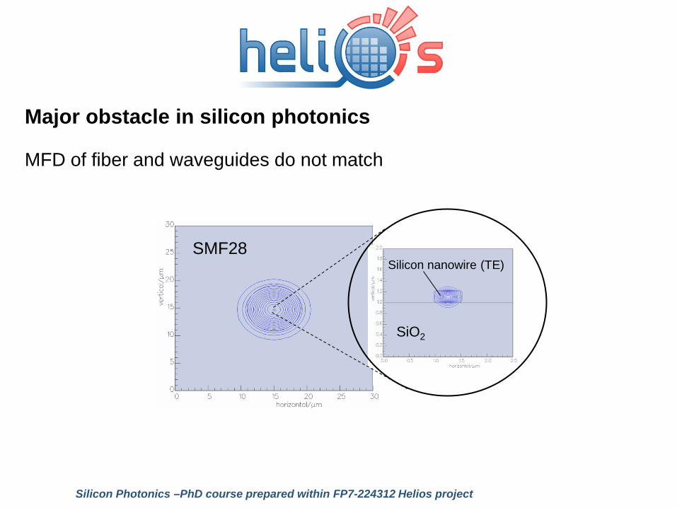
SMF28
SiO2
Silicon nanowire (TE)
Major obstacle in silicon photonics
MFD of fiber and waveguides do not match
Silicon Photonics –PhD course prepared within FP7-224312 Helios project

This requires
Spotsize conversion structures
Lateral coupling Vertical coupling
h
Buried Oxide
Substrate
g r e
φ
fiber
d
x
zy
air
• typically based on inverted tapers• spotsize: ~3 µm
• typically based on gratings• spotsize: ~ 10 µm
Silicon Photonics –PhD course prepared within FP7-224312 Helios project

Inverted taper – example SiN waveguide geometry at end of taperHxW=3µmx3µm (SiNx), on SiO2 (1µm)
Lateral - single fiber coupling issues
• MFD too small for standard fiber
• require lensed fiber
• what are alignment tolerances?
Silicon Photonics –PhD course prepared within FP7-224312 Helios project
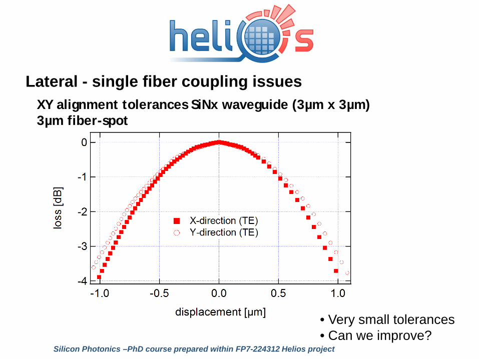
XY alignment tolerances SiNx waveguide (3µm x 3µm) 3µm fiber-spot
• Very small tolerances• Can we improve?
Lateral - single fiber coupling issues
Silicon Photonics –PhD course prepared within FP7-224312 Helios project
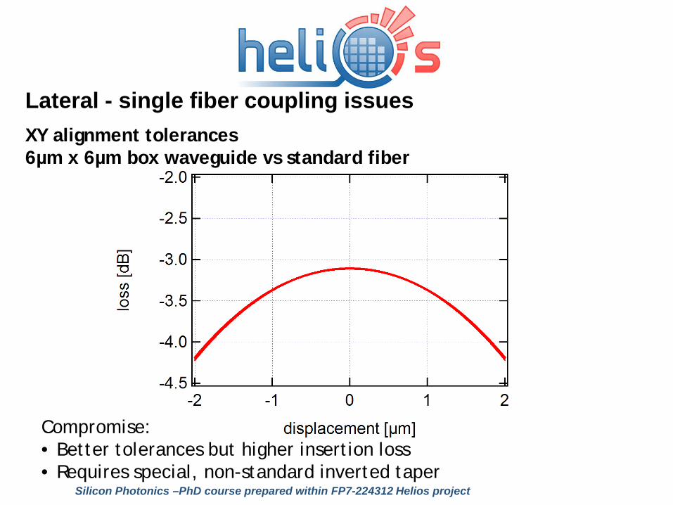
XY alignment tolerances 6µm x 6µm box waveguide vs standard fiber
Compromise:• Better tolerances but higher insertion loss• Requires special, non-standard inverted taper
Lateral - single fiber coupling issues
Silicon Photonics –PhD course prepared within FP7-224312 Helios project

Displacement 1-2 µmPenalty < 1 dB
1D grating couplerXY alignment tolerances (measured)
Vertical - single fiber coupling issues
Silicon Photonics –PhD course prepared within FP7-224312 Helios project

How about z-dependency?• approximation by Gaussian beam analysis• lensed fibers deliver Gaussian beam• most important parameter: spotsize (beam width) w
( )2
0 1
+⋅=
Rzzwzw
λπ 2
00
wz = Rayleighparameter
Assuming that the beam intensity scales approximately
we would lose about 3dB at the Rayleigh distance
if the beam waist were exactly matched to the waveguide MFD.
Z-dependency is generally weaker than XY- dependency
2w∝
beam waist
Silicon Photonics –PhD course prepared within FP7-224312 Helios project

Single fiber coupling – intermediate summary
• lateral coupling with realistic XY-tolerances of 0.5µm/dB
• vertical coupling with realistic XY-tolerances of 1.5 µm/dB
• lateral coupling requires lensed fibers for low loss
• vertical coupling can be done using standard fiber butts
Silicon Photonics –PhD course prepared within FP7-224312 Helios project
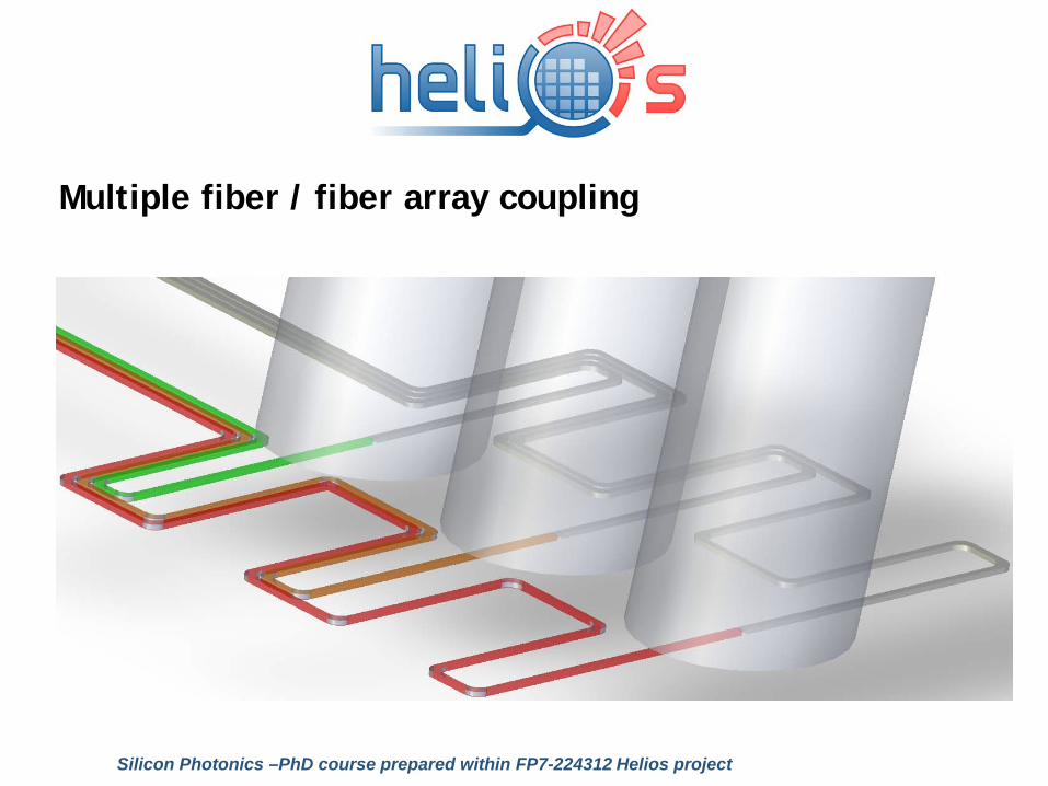
Multiple fiber / fiber array coupling
Silicon Photonics –PhD course prepared within FP7-224312 Helios project
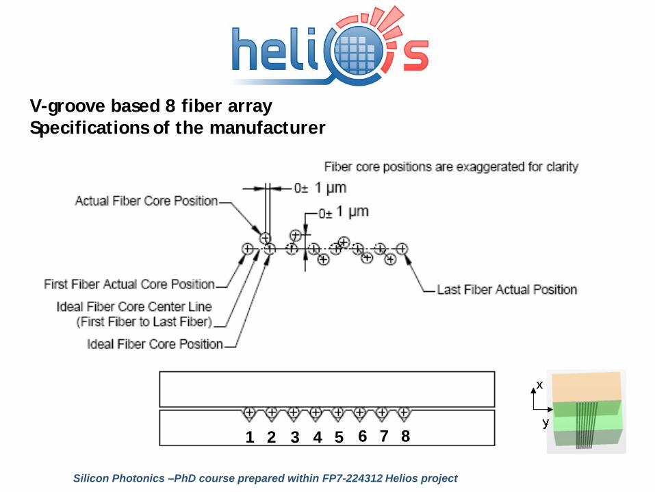
V-groove based 8 fiber arraySpecifications of the manufacturer
1 2 3 4 5 6 7 8
Silicon Photonics –PhD course prepared within FP7-224312 Helios project

V-groove fiber array experiment
XY-Scanned Fiber PositionsSilicon Photonics –PhD course prepared within FP7-224312 Helios project

pitch
vertical
Measured misalignment of fibers in v-groove array
V-groove fiber array experiment
• measured toleranced are not the best possible, but typical• fiber array tolerances too large for present lateral coupling structures• tolerance-wise vertical couplers are favorable• how can it be implemented?• (not mentioned here other issues of grating such as polarization dependence etc)
Silicon Photonics –PhD course prepared within FP7-224312 Helios project

Fiber array package - concept
• coupling to fully passive SOI chip
Silicon Photonics –PhD course prepared within FP7-224312 Helios project
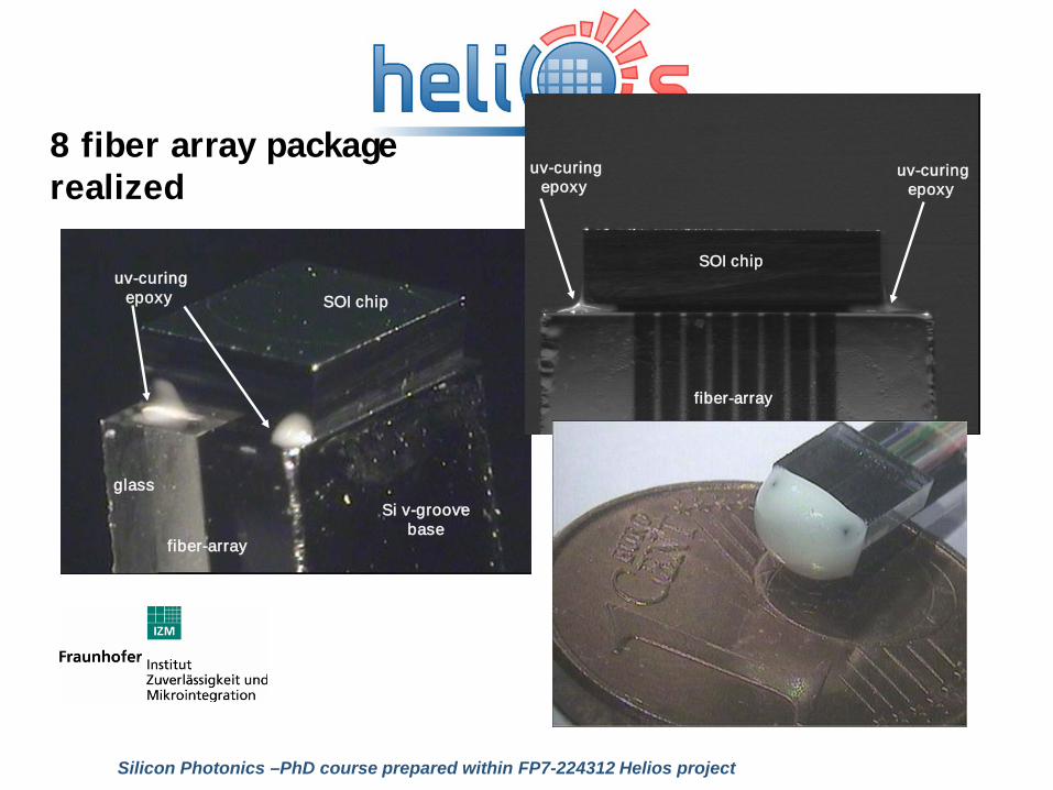
uv-curingepoxy
fiber-array
SOI chip
Si v-groovebase
glass
uv-curingepoxy
fiber-array
SOI chip
Si v-groovebase
glass
uv-curingepoxy
fiber-array
SOI chip
uv-curingepoxy
uv-curingepoxy
fiber-array
SOI chip
uv-curingepoxy
8 fiber array packagerealized
Silicon Photonics –PhD course prepared within FP7-224312 Helios project
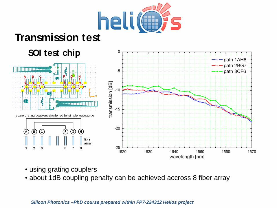
SOI test chip
Transmission test
• using grating couplers• about 1dB coupling penalty can be achieved accross 8 fiber array
Silicon Photonics –PhD course prepared within FP7-224312 Helios project

First approach to handling electrical & optical i/o
• enable multiple (~ 30) optical i/o• multiple (~ 60) electrical LF i/o• match ePIXfab standard chip size• plug in a testbed
g-Pack
Silicon Photonics –PhD course prepared within FP7-224312 Helios project

Example – g-Pack
Silicon Photonics –PhD course prepared within FP7-224312 Helios project

Future of silicon photonic packaging
• merging electronic & photonics technologies
• optical packaging needs to undergo a paradigm change
• costs will need to be reduced by 1-2 orders of magnitude
• up to now, low cost means single fiber or multi-mode fiber
Silicon Photonics –PhD course prepared within FP7-224312 Helios project

Acknowledgements
• Tolga Tekin & Henning Schroeder from Fraunhofer IZM, Berlin
• Pieter Dumon & Wim Bogaerts from Uni Ghent
• Karsten Voigt from Technische Uni Berlin
Silicon Photonics –PhD course prepared within FP7-224312 Helios project