Ch02 AVR Architecture
26
Embedded Systems Engr. Rashid Farid Chishti e-mail: [email protected] Chapter 02: AVR Architecture and Assembly Language Programming International Islamic University H-10, Islamabad, Pakistan http://www.iiu.edu.pk
-
Upload
syed-kawish-quyyum -
Category
Documents
-
view
226 -
download
1
description
kasdflkjsadflkasdfj;lk
Transcript of Ch02 AVR Architecture

Embedded Systems
Engr. Rashid Farid Chishtie-mail:
Chapter 02: AVR Architecture and Assembly
Language Programming
International Islamic University H-10, Islamabad, Pakistan
http://www.iiu.edu.pk
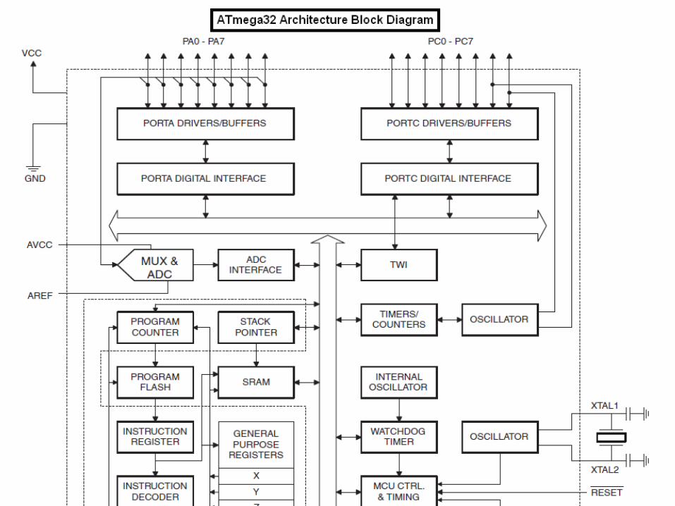
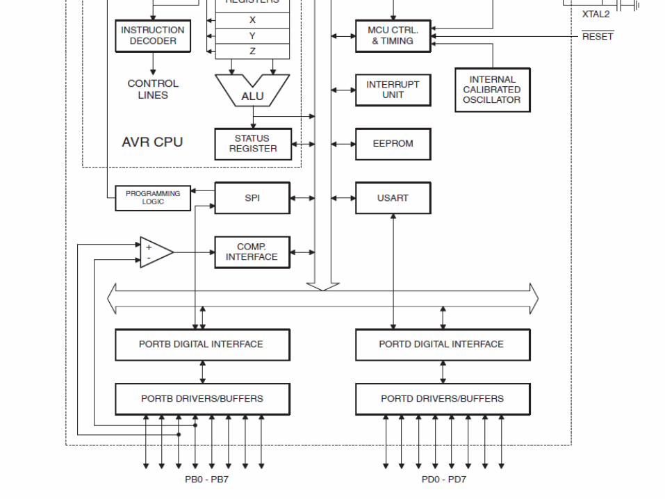
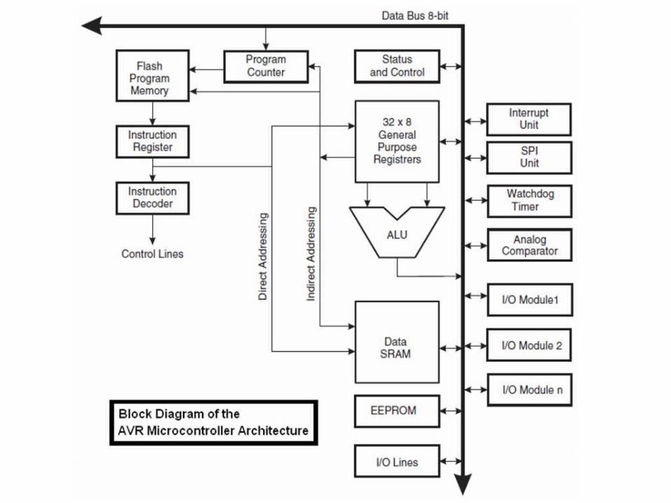
AVR’s CPUAVR’s CPU
ALU32 General Purpose registers(R0 to R31)PC registerInstruction decoder
CPUPC
ALU
registers
R1
R0
R15
R2
…
R16
R17
…
R30
R31
Instruction Register
Instruction decoder
SREG: I T H S V N CZ
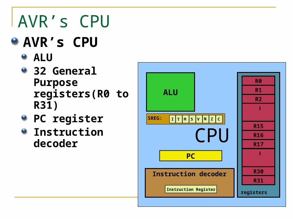
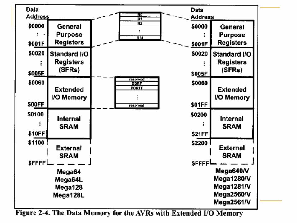
Two kinds of memory space in AVR: code memory spacedata memory space.
program is stored in
code memory space,
whereas the data
memory stores data.
The data memory is composed of three parts:GPRs (general purpose registers)SFR (I/O Registers)SRAM (general purpose RAM)
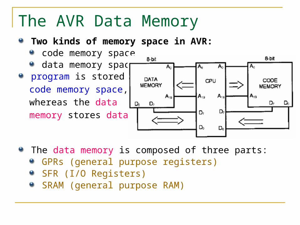
The AVR Data Memory
$0000$0001
$0020
General purpose
RAM(SRAM)
R0R1R2
$001F
$005F
R31
...
TWBRTWSR
SPHSREG
...
General Purpose Registers
Standard I/ORegisters
$00$01
$3E$3F
$0060
...
...
Data Address Space
I/O Address
...
8 bit
$FFFF
Figure 2-3:The Data Memory for AVRs with no Extended I/O memory
SREG
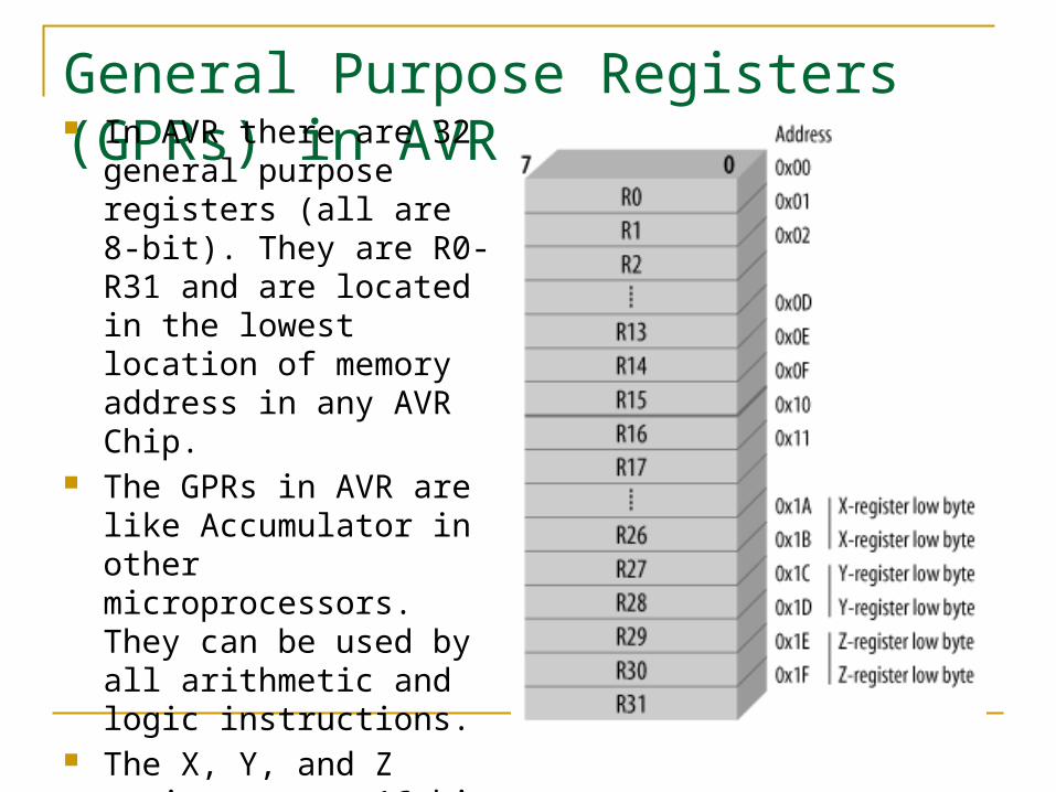
General Purpose Registers (GPRs) in AVR In AVR there are 32
general purpose registers (all are 8-bit). They are R0-R31 and are located in the lowest location of memory address in any AVR Chip.
The GPRs in AVR are like Accumulator in other microprocessors. They can be used by all arithmetic and logic instructions.
The X, Y, and Z registers are 16-bit address pointers for indirect addressing of the Data Space (RAM).

I/O Registers (SFRs) in AVR The I/O memory is dedicated to specific functions such
as status register, timers, serial communication, I/O ports, ADC, and so on.
The function of each I/O memory location is fixed by the CPU designer at the time of design because it is used for control of the microcontroller or peripherals.
All of the AVRs have at least 64 bytes of I/O memory locations. This 64-byte section is called standard I/O memory.
In AVRs with more than 32 I/O pins (e.g., ATmega64, ATmegal28, and ATmega256) there is also an extended I/O memory, which contains the registers for controlling the extra ports and the extra peripherals.

NameAddressI/O Mem.$00 $20 TWBR$01 $21 TWSR
$04 $24 ADCL$05 $25 ADCH
$02 $22 TWAR$03 $23 TWDR
$06 $26 ADCSRA$07 $27 ADMUX$08 $28 ACSR$09 $29 UBRRL$0A $2A UCSRB$0B $2B UCSRA$0C $2C UDR$0D $2D SPCR$0E $2E SPSR$0F $2F
PIND$10 $30DDRD$11 $31
PORTD$12 $32PINC$13 $33DDRC$14 $34
PORTC$15 $35
PINB$16 $36DDRB$17 $37
PORTB$18 $38PINA$19 $39DDRA$1A $3A
PORTA$1B $3BEECR$1C $3C
EEDR$1D $3D
EEARL$1E $3EEEARH$1F $3F
SPDR
NameAddressI/O Mem.
NameAddressI/O Mem.
UBRRC$20 $40
UBRRH$21 $41 WDTCR$22 $42 ASSR$23 $43 OCR2$24 $44 TCNT2$25 $45 TCCR2$26 $46 ICR1L$27 $47 ICR1H$28 $48 OCR1BL$29 $49 OCR1BH
OCR1AH$2B $4B
SFIOR$30 $50
OCDR$31 $51
OSCCAL$32 $52
TCCR0$33 $53MCUCSR$34 $54MCUCR$35 $55TWCR$36 $56
SPMCR$37 $57TIFR$38 $58
TIMSK$39 $59
TCNT1L$2C $4CTCNT1H$2D $4DTCCR1B$2E $4ETCCR1A$2F $4F
TCNT0
$3A $5AGICR$3B $5BOCR0$3C $5CSPL$3D $5DSPH$3E $5E
GIFR
OCR1AL$2A $4A SREG$3E $5E
Note: Although memory address $20-$5F is set aside for I/O registers (SFR) we can access them as I/O locations with addresses starting at $00.
Figure 2-7. I/O registers of the ATmega32 and their Data Memory Address Locations
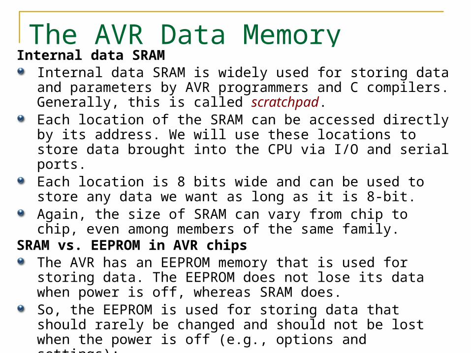
The AVR Data MemoryInternal data SRAM
Internal data SRAM is widely used for storing data and parameters by AVR programmers and C compilers. Generally, this is called scratchpad.Each location of the SRAM can be accessed directly by its address. We will use these locations to store data brought into the CPU via I/O and serial ports.Each location is 8 bits wide and can be used to store any data we want as long as it is 8-bit.Again, the size of SRAM can vary from chip to chip, even among members of the same family.
SRAM vs. EEPROM in AVR chipsThe AVR has an EEPROM memory that is used for storing data. The EEPROM does not lose its data when power is off, whereas SRAM does.So, the EEPROM is used for storing data that should rarely be changed and should not be lost when the power is off (e.g., options and settings);

The AVR Data MemorySRAM vs. EEPROM in AVR chips
The SRAM is used for storing data and parameters that are changed frequently. The three parts of the data memory (GPRs, SFRs, and the internal SRAM) are made of SRAM. By adding the sizes of GPR, SFRs (I/O registers), and SRAMs we get the data memory size.
Table 2-1: Data Memory Size for AVR Chips
Microcontroller Data Memory (Bytes)
I/O Registers(Bytes)
SRAM(Bytes)
General PurposeRegister
ATtiny25 224 64 128 32
ATtiny85 608 64 512 32
Atmega8 1120 64 1024 32
Atmega16 1120 64 1024 32
ATmega32 2144 64 2048 32
ATmega128 4352 64+160 4094 32
ATmega2560 8704 64+416 8192 32

GPRs and ALU
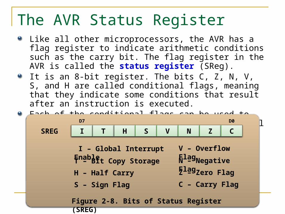
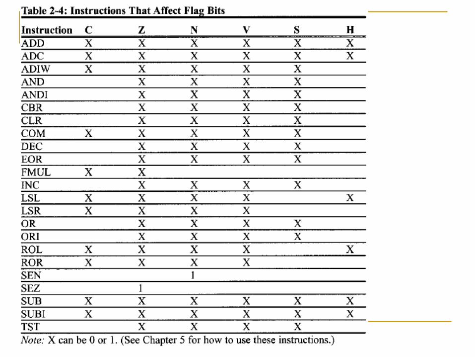
The AVR Status RegisterLike all other microprocessors, the AVR has a flag register to indicate arithmetic conditions such as the carry bit. The flag register in the AVR is called the status register (SReg).It is an 8-bit register. The bits C, Z, N, V, S, and H are called conditional flags, meaning that they indicate some conditions that result after an instruction is executed.Each of the conditional flags can be used to perform a conditional branch (jump), as we will see in Chapters 3 and 5.
I T H S V N Z C
D0D7
SREG
I – Global Interrupt Enable V – Overflow Flag
T – Bit Copy Storage N – Negative Flag
H – Half Carry Z – Zero Flag
S – Sign Flag C – Carry Flag
Figure 2-8. Bits of Status Register (SREG)
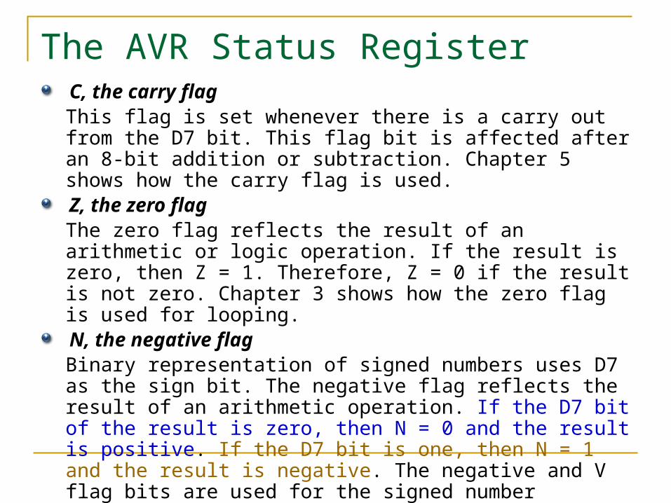
The AVR Status RegisterC, the carry flagThis flag is set whenever there is a carry out from the D7 bit. This flag bit is affected after an 8-bit addition or subtraction. Chapter 5 shows how the carry flag is used.Z, the zero flagThe zero flag reflects the result of an arithmetic or logic operation. If the result is zero, then Z = 1. Therefore, Z = 0 if the result is not zero. Chapter 3 shows how the zero flag is used for looping.N, the negative flagBinary representation of signed numbers uses D7 as the sign bit. The negative flag reflects the result of an arithmetic operation. If the D7 bit of the result is zero, then N = 0 and the result is positive. If the D7 bit is one, then N = 1 and the result is negative. The negative and V flag bits are used for the signed number arithmetic operations and are discussed in Chapter 5.
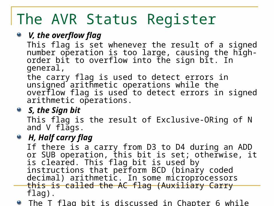
The AVR Status RegisterV, the overflow flagThis flag is set whenever the result of a signed number operation is too large, causing the high-order bit to overflow into the sign bit. In general,the carry flag is used to detect errors in unsigned arithmetic operations while the overflow flag is used to detect errors in signed arithmetic operations. S, the Sign bitThis flag is the result of Exclusive-ORing of N and V flags. H, Half carry flagIf there is a carry from D3 to D4 during an ADD or SUB operation, this bit is set; otherwise, it is cleared. This flag bit is used by instructions that perform BCD (binary coded decimal) arithmetic. In some microprocessors this is called the AC flag (Auxiliary Carry flag).The T flag bit is discussed in Chapter 6 while Chapter 10 covers the I flag.

15
Experimentation with Condition Flags (#1/3)Indicate the changes in N, Z, C, V flags for the following arithmetic operations: (Assume 4 bit-numbers)
1 1 111 0010 0011 + 1010 1111----------- 1101 0010
N = 1 V = 0 Z = 0 C = 0 S = 1 H = 1
16
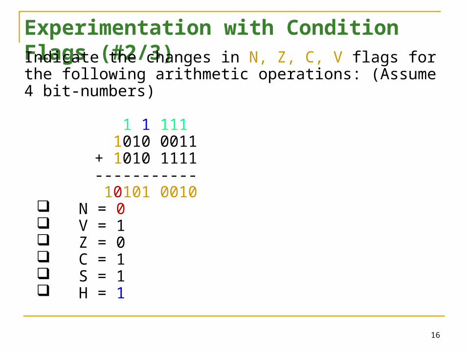
Experimentation with Condition Flags (#2/3)Indicate the changes in N, Z, C, V flags for the following arithmetic operations: (Assume 4 bit-numbers)
1 1 111 1010 0011+ 1010 1111----------- 10101 0010
N = 0 V = 1 Z = 0 C = 1 S = 1 H = 1
17
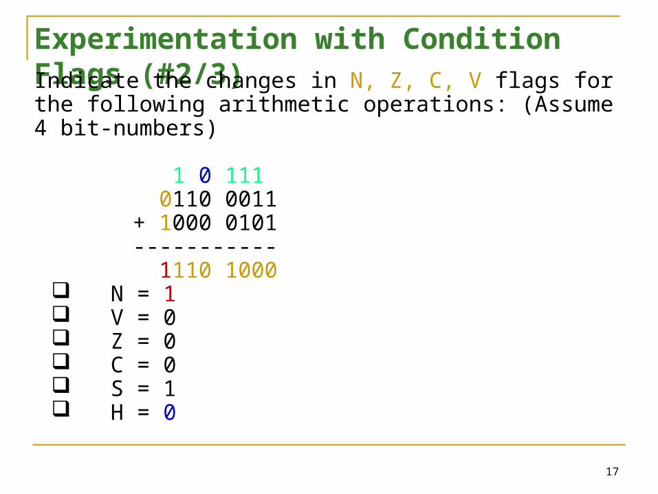
Experimentation with Condition Flags (#2/3)Indicate the changes in N, Z, C, V flags for the following arithmetic operations: (Assume 4 bit-numbers)
1 0 111 0110 0011 + 1000 0101 ----------- 1110 1000
N = 1 V = 0 Z = 0 C = 0 S = 1 H = 0

Features of ATmega32 Microcontroller8-bit RISC AVR microcontroller with 32KB In-System Self-
programmable Flash program memory, 2KB SRAM and 1KB EEPROM.32x8 General Purpose RegistersUp to 16 MIPS Throughput at 16 MHzTwo 8-bit Timer/Counters with Separate Prescalers and Compare ModesOne 16-bit Timer/Counter with Separate Prescaler, Compare Mode, and Capture Mode8-channel, 10-bit ADC, 4 PWM ChanelsByte-oriented Two-wire Serial InterfaceProgrammable Serial USARTMaster/Slave SPI Serial Interface
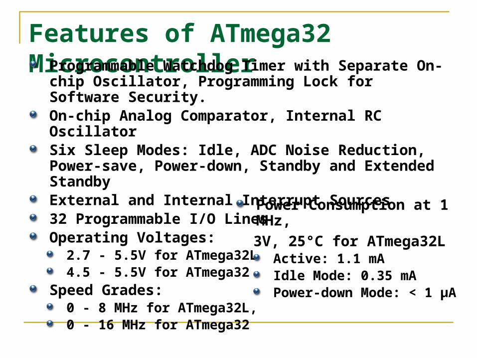
Features of ATmega32 MicrocontrollerProgrammable Watchdog Timer with Separate On-chip
Oscillator, Programming Lock for Software Security.On-chip Analog Comparator, Internal RC OscillatorSix Sleep Modes: Idle, ADC Noise Reduction, Power-save, Power-down, Standby and Extended StandbyExternal and Internal Interrupt Sources32 Programmable I/O LinesOperating Voltages:
2.7 - 5.5V for ATmega32L4.5 - 5.5V for ATmega32
Speed Grades:0 - 8 MHz for ATmega32L, 0 - 16 MHz for ATmega32
Power Consumption at 1 MHz,
3V, 25°C for ATmega32LActive: 1.1 mAIdle Mode: 0.35 mAPower-down Mode: < 1 μA

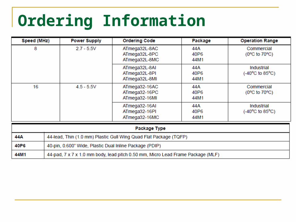
Ordering Information

26
Package Types
Tuesday, April 18, 2023 www.iiu.edu.pk
TQFP (Thin Plastic Quad Flat Package )
Holder PLCC ( Plastic leadless Chip Carrier )
PDIP (Plastic Dual Inline Package )
MLF (Micro Lead frame Package)


![AVR Architecture [Lect-03 Fall09]](https://static.fdocuments.in/doc/165x107/577dab4c1a28ab223f8c3b24/avr-architecture-lect-03-fall09.jpg)