Ch. 12: Crystalline Solids and Modern...
40
Ch. 12: Crystalline Solids and Modern Materials Dr. Namphol Sinkaset Chem 200: General Chemistry I
Transcript of Ch. 12: Crystalline Solids and Modern...

Ch. 12: Crystalline Solids and Modern Materials
Dr. Namphol Sinkaset Chem 200: General Chemistry I

I. Chapter Outline
I. Introduction II. X-Ray Crystallography III. Unit Cells and Basic Structures IV. Types of Crystalline Solids V. Semiconductors and Band Theory

I. Materials Science • Materials of the day literally shape
society. • History of metallurgy: from gold to
copper to bronze to iron to steel. • Porcelain revolutionizes dishware. • Cement revolutionizes construction. • Semiconductors gives us today’s
society.

II. Crystalline Solids • Recall that crystalline solids have atoms
or molecules arranged with long-range order.
• Sharp angles and edges in minerals are dictated by specific patterns at the atomic and molecular level.
• Structure of crystalline solids can be determined with x-ray crystallography.

II. Interference
• Recall that EM radiation can constructively or destructively interfere.
• When coupled with diffraction, interference patterns form.

II. X-ray Diffraction
• Method to find spacing between planes, d. • Ray 2 travels a distance that is 2a longer
than Ray 1. • If 2a is an integral # of wavelengths, rays
will be in phase.

II. Bragg’s Law • We derive an important equation used
to solve crystal structures.
𝑛𝑛λ = 2𝑎𝑎 Necessary for constructive interference
sin θ =𝑎𝑎𝑑𝑑
𝑎𝑎 = 𝑑𝑑 sin θ
𝑛𝑛λ = 2𝑑𝑑 sin θ

II. Finding d Between Layers
• Rearrangement of Bragg’s law allows calculation of d.
• X-ray crystallography involves creating diffraction patterns from different angles to find the entire crystalline structure.
𝑑𝑑 =𝑛𝑛λ
2 sin θ
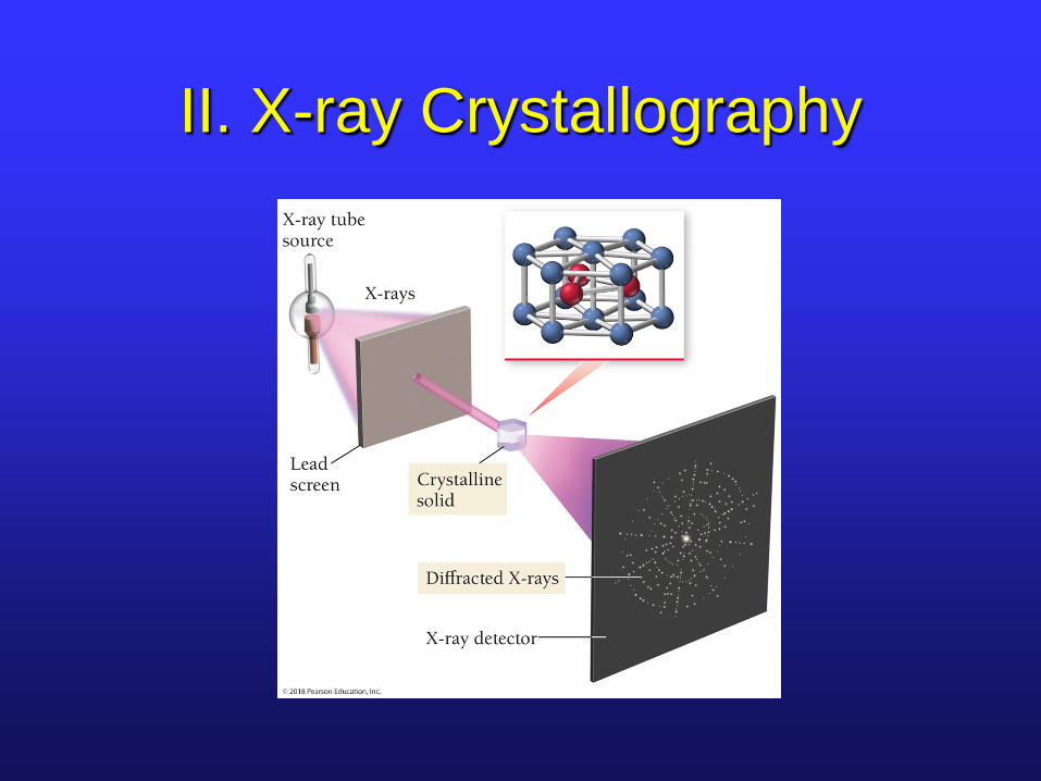
II. X-ray Crystallography

III. Unit Cells
• X-ray crystallography reveals the crystalline lattice, how atoms are regularly spaced in a crystalline solid.
• To represent this lattice in the simplest way possible, we use unit cells.
• If a unit cell is repeated, it will reconstruct the entire crystalline lattice.

III. Unit Cells as a Base Unit
• Unit cells are 3D analogs of floor tiles. • Individual floor tiles together create an
extended pattern.

III. Simple Cubic Unit Cell

III. Body-Centered Cubic Unit Cell
• Colored spheres are used for clarity; each sphere is the same atom!

III. Face-Centered Cubic Unit Cell

III. Summary of Cubic Unit Cells

III. Closest-Packed Structures
• Another way to envision crystal structures is to think about it as stacking layers – like fruit at grocery store.
• This is useful in atomic solids like metals.
• There are different ways we can “pack” these atoms.

III. Simple Cubic Packing
• For example, we can stack atoms directly on top of each other.
• This packing is the same as a simple cubic unit cell.
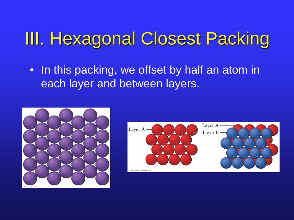
III. Hexagonal Closest Packing • In this packing, we offset by half an atom in
each layer and between layers.

III. Hexagonal Closest Packing
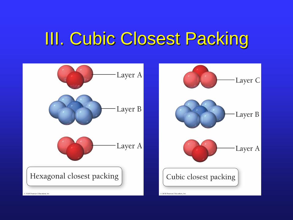
III. Cubic Closest Packing
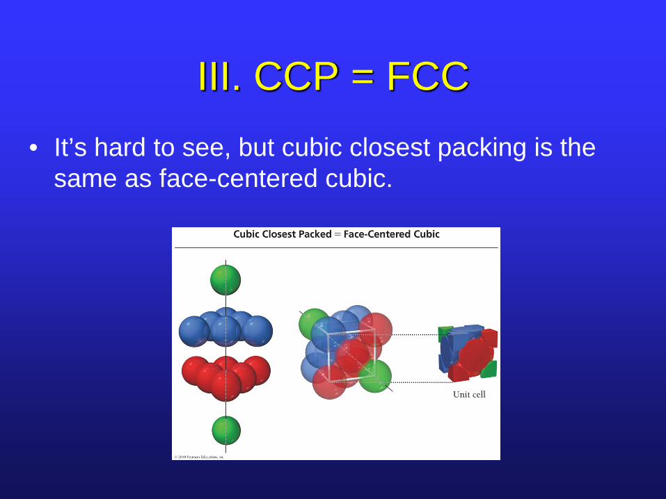
III. CCP = FCC • It’s hard to see, but cubic closest packing is the
same as face-centered cubic.

IV. Types of Crystalline Solids

IV. Structures of Ionic Solids
• Crystalline structures of ionics are closely related to the unit cells we covered.
• Three things need to be accommodated: Maximize coordination number Electroneutrality Relative sizes of cation and anion

IV. Cesium Chloride • The ions of cesium chloride are of similar size
(radii of 167 pm and 181 pm, respectively). • BCC-type structure maximizes coordination
number (8) and keeps electroneutrality.

IV. Sodium Chloride
• Na+ and Cl- are not so similar in size, 97 and 181 pm, respectively.
• Cl-’s are FCC and Na+’s occupy holes in between for CN = 6.
• Known as rock salt structure.

IV. Zinc Blende
• In ZnS the radii are 74 and 184 pm, respectively.
• S2-’s are FCC and Zn2+’s occupy tetrahedral holes (CN = 4).

IV. Fluorite and Antifluorite
• For 1:2 ionics like CaF2, Ca2+’s are FCC with F-’s occupying 8 tetrahedral holes.
• Antifluorite would be for 2:1 ionics.

IV. Metallic Atomic Solids
• Metallic solids are held together via metallic bonds.
• Metal atoms donate valence e- to an e- “sea.”
• Metal cations float in this “sea of e-’s.”

IV. Malleability of Metals
• This e- sea model of metals explains the malleability of metals.
IV. Explaining Other Properties of Metals
• Group 2 metals have higher melting points than group 1 metals.
• Metals have high electrical conductivity. • Metals conduct heat well.

IV. Network Covalent Solids
• These are solids in which atoms are held together with covalent bonds.
• Network solids have very high melting points due to extended covalent bonding.
• Two most common examples are the different allotropes of carbon and silicates.
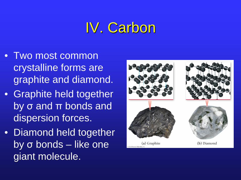
IV. Carbon
• Two most common crystalline forms are graphite and diamond.
• Graphite held together by σ and π bonds and dispersion forces.
• Diamond held together by σ bonds – like one giant molecule.

IV. Silicates • Silicates are extended arrays of Si and O. • These are the most common network solids. • Si single bonds to 4 O’s in a tetrahedral
arrangement.

V. Semiconductors
• To explain semiconductors, we apply molecular orbital theory to atoms in crystalline solid.
• When two atomic orbitals are combined, how many molecular orbitals form?
• We extend this idea to a large number of atomic orbitals.

V. Band Theory • As more molecular orbitals are formed,
they start to coalesce into a band. • These bands extend across the entire
crystalline solid.
V. Promotion to Conduction Band
• If there’s a small or no band gap, it’s easy for an e- to jump into the conduction band if the T is high enough.
• Once there, it’s free to move along the entire solid.
• This freedom of movement explains high thermal and electrical conductivity.

V. Importance of the Band Gap
• The band gap determines whether the material is a conductor, semiconductor, or insulator.

V. Doped Semiconductors
• Si has a fairly large band gap, so only a few e-’s are promoted to the conduction band at room T; thus, it is a poor electrical conductor.
• We can add a small amount of a different element to improve it’s conductivity.
• This process is called doping.

V. n-Type Semiconductors
• If we add some P to Si, it brings an extra valence e-.
• This extra e- must go into the conduction band because the valence band is full.
• This doped Si now conducts well. • Called n-type because have electrons
as negative charge carriers.

V. p-Type Semiconductors • We could also add Ga to Si to increase
the conductivity. • Ga has one less e-, so it creates holes
(empty MO’s) in the valence band. • Since e-’s can now move from hole to
hole, this doped Si is a better conductor. • Called p-type because each hole acts
as a positive charge that moves in the opposite direction of the e-’s.