CFP MSA CFP2 Hardware Specificationcfp-msa.org/Documents/CFP2_HW-Spec-rev1.0.pdf · Page 2 CFP MSA...
64
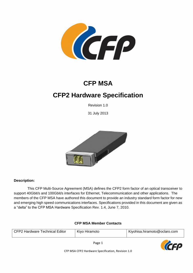
Page 1 CFP MSA CFP2 Hardware Specification, Revision 1.0 CFP MSA CFP2 Hardware Specification Revision 1.0 31 July 2013 Description: This CFP Multi-Source Agreement (MSA) defines the CFP2 form factor of an optical transceiver to support 40Gbit/s and 100Gbit/s interfaces for Ethernet, Telecommunication and other applications. The members of the CFP MSA have authored this document to provide an industry standard form factor for new and emerging high speed communications interfaces. Specifications provided in this document are given as a “delta” to the CFP MSA Hardware Specification Rev. 1.4, June 7, 2010. CFP MSA Member Contacts CFP2 Hardware Technical Editor Kiyo Hiramoto [email protected]
Transcript of CFP MSA CFP2 Hardware Specificationcfp-msa.org/Documents/CFP2_HW-Spec-rev1.0.pdf · Page 2 CFP MSA...
Page 1
CFP MSA CFP2 Hardware Specification, Revision 1.0
CFP MSA
CFP2 Hardware Specification
Revision 1.0
31 July 2013
Description:
This CFP Multi-Source Agreement (MSA) defines the CFP2 form factor of an optical transceiver to
support 40Gbit/s and 100Gbit/s interfaces for Ethernet, Telecommunication and other applications. The
members of the CFP MSA have authored this document to provide an industry standard form factor for new
and emerging high speed communications interfaces. Specifications provided in this document are given as
a “delta” to the CFP MSA Hardware Specification Rev. 1.4, June 7, 2010.
CFP MSA Member Contacts
CFP2 Hardware Technical Editor Kiyo Hiramoto [email protected]

Page 2
CFP MSA CFP2 Hardware Specification, Revision 1.0
Avago Technologies, Ltd. John Petrilla [email protected]
Finisar Corp. Chris Cole [email protected]
Fujitsu Optical Components, Ltd. Yasunori Nagakubo [email protected]
Oclaro, Inc. Kiyo Hiramoto [email protected]
Sumitomo Electric Industries, Ltd. Eddie Tsumura [email protected]
Page 3
CFP MSA CFP2 Hardware Specification, Revision 1.0
CONTENTS
REVISION HISTORY ............................................................................................................................................................. 6
TABLE LIST............................................................................................................................................................................ 7
FIGURE LIST .......................................................................................................................................................................... 9
REFERENCE DOCUMENTS............................................................................................................................................... 11
1 GENERAL ..................................................................................................................................................................... 12
1.1 SCOPE .......................................................................................................................................................................... 12
1.1.1 Application & Qualification ...................................................................................................................................... 12
1.2 CFP2 FUNCTIONAL BLOCK DIAGRAM .................................................................................................................. 12
1.3 FUNCTIONAL DESCRIPTION ................................................................................................................................... 13
1.3.1 Hot Pluggable ........................................................................................................................................................... 13
2 CFP2 HARDWARE SIGNALING PINS ...................................................................................................................... 13
2.1 HARDWARE CONTROL PINS ........................................................................................................................................... 14
2.2 HARDWARE CONTROL PINS: FUNCTIONAL DESCRIPTION ............................................................................................. 14
2.2.1 Programmable Controls (PRG_CNTLs) ............................................................................................................... 15
2.3 HARDWARE ALARM PINS ................................................................................................................................................ 15
2.4 HARDWARE ALARM PINS: FUNCTIONAL DESCRIPTION .................................................................................................. 16
2.5 MANAGEMENT INTERFACE PINS (MDIO) ....................................................................................................................... 16
2.6 CFP2 MANAGEMENT INTERFACE HARDWARE DESCRIPTION ....................................................................................... 18
2.6.1 MDIO Physical Port Addresses ............................................................................................................................. 18
2.7 HARDWARE SIGNALING PIN ELECTRICAL SPECIFICATIONS ........................................................................................... 19
2.8 HARDWARE SIGNALING PIN TIMING REQUIREMENTS .................................................................................................... 19
3 MODULE MANAGEMENT INTERFACE DESCRIPTION ......................................................................................... 21
Page 4
CFP MSA CFP2 Hardware Specification, Revision 1.0
4 PERFORMANCE SPECIFICATIONS ......................................................................................................................... 22
4.1 OPERATING ENVIRONMENT .................................................................................................................................. 22
4.2 POWER SUPPLIES AND POWER DISSIPATION ................................................................................................. 22
4.2.1 Voltage power supply and power dissipation ...................................................................................................... 22
4.2.2 Inrush current ........................................................................................................................................................... 22
4.2.3 Turn-off current ........................................................................................................................................................ 22
4.2.4 Power Supply Noise Susceptibility ........................................................................................................................ 22
4.2.5 Grounding ................................................................................................................................................................. 25
4.3 OPTICAL CHARACTERISTICS ................................................................................................................................. 25
4.3.1 Optical specifications .............................................................................................................................................. 25
4.4 HIGH SPEED ELECTRICAL CHARACTERISTICS ................................................................................................ 25
4.4.1 25 Gbit/s Transmitter Data (and Clock) ................................................................................................................ 26
4.4.2 25 Gbit/s Receiver Data (and Clock) .................................................................................................................... 26
4.4.3 10 Gbit/s Transmitter Data (and Clock) ................................................................................................................ 26
4.4.4 10 Gbit/s Receiver Data (and Clock) .................................................................................................................... 27
4.4.5 Loopback (Optional) ................................................................................................................................................ 27
4.4.6 Reference Clock ...................................................................................................................................................... 28
4.4.7 Transmitter Monitor Clock (Option) ....................................................................................................................... 29
4.4.8 Receiver Monitor Clock (Option) ........................................................................................................................... 29
5 MECHANICAL SPECIFICATIONS ............................................................................................................................. 35
5.1 MECHANICAL OVERVIEW ................................................................................................................................................ 35
5.2 ELECTRICAL CONNECTOR .............................................................................................................................................. 36
Page 5
CFP MSA CFP2 Hardware Specification, Revision 1.0
5.2.1 Module Plug Connector .......................................................................................................................................... 36
5.2.2 Host Connector ........................................................................................................................................................ 37
5.2.3 Connector Pin Contact Mating ............................................................................................................................... 39
5.3 CFP2 MODULE DIMENSIONS ......................................................................................................................................... 41
5.3.1 CFP2 Mechanical Surface Characteristics .......................................................................................................... 43
5.3.2 CFP2 Insertion & Extraction ................................................................................................................................... 43
5.4 HOST SYSTEM DIMENSIONS........................................................................................................................................... 44
5.5 RIDING HEAT SINK.......................................................................................................................................................... 44
5.6 OPTICAL CONNECTORS .................................................................................................................................................. 47
5.6.1 Optional Optical LC Connector Position for Telecom Applications .................................................................. 48
5.7 ELECTRICAL CONNECTORS ............................................................................................................................................ 49
5.8 PIN ASSIGNMENT ............................................................................................................................................................ 49
5.9 CFP2 BAIL LATCH COLOR CODING AND LABELING ...................................................................................................... 57
6 REGULATORY COMPLIANCE .................................................................................................................................. 64
Page 6
CFP MSA CFP2 Hardware Specification, Revision 1.0
REVISION HISTORY
Draft Date Revised Items
0.0 Nov. 30, 2012 Initial draft, based on CFP2 Baseline Design, Release 1
0.1 Dec. 14, 2012 Edits from CFP MSA System OEM Reviewers comments -
0.2 Mar. 14, 2013
Added Table 2-5: Timing Parameters for CFP Hardware Signal Pins.
Add Power Class 5 & 6 in Table 4-1 Voltage power supply
Added future high speed electrical interface in Section 4.4.
Changed Figure 4-1 to include common mode impedance termination.
Changed REFCLK alternatives in Table 4-4 to be in line with what are specified in the MDIO specification.
0.3 Apr. 25, 2013
Added Figure 2-1 and Figure 2-2
Modified Figure 5-7, Figure 5-8 and Figure 5-10 according to the latest published CFP2 baseline drawing
Added maximum weight value in Table 5-1
Replaced TBD with actual values in Table 5-2
1.0 Jul. 31, 2013 Added Table 5-7 & Table 5-10 for multi-port application
Page 7
CFP MSA CFP2 Hardware Specification, Revision 1.0
TABLE LIST
Table 2-1: Control Pins ............................................................................................................................... 9
Table 2-2: CFP2 Module Power Classes defined by Hardware Interlock .................................................. 15
Table 2-3: Hardware Alarm Pins ............................................................................................................... 16
Table 2-4: Management Interface Pins (MDIO) ........................................................................................ 17
Table 2-5: Timing Parameters for CFP Hardware Signal Pins ........................................................................ 17
Table 4-1 Voltage power supply ............................................................................................................... 23
Table 4-2: Optional Reference Clock Characteristics................................................................................ 28
Table 4-3: Optional Transmitter & Receiver Monitor Clock Characteristics ............................................... 30
Table 4-4: CFP2 Module Clocking Signals ............................................................................................... 19
Table 5-1: CFP2 Mechanical Characteristics ............................................................................................ 43
Table 5-2: CFP2 Module Insertion, Extraction Forces............................................................................... 44
Table 5-3: Optical Connectors .................................................................................................................. 28
Table 5-4 CFP2 Host Connector Assembly .............................................................................................. 29
Table 5-5: CFP2 N x 25 Gbit/s Pin-Map ................................................................................................... 63
Table 5-6: CFP2 10 x 10 Gbit/s Pin-Map .................................................................................................. 51
Table 5-7: CFP2 CFP2 Multi-Port Pin-Map ....................................................................................................... 51
Table 5-8: CFP2 Bottom Row Pin Description for N x 25 Gbit/s applications ............. Error! Bookmark not
defined.
Table 5-9: CFP2 Bottom Row Pin Description for 10 x 10 Gbit/s applications ........................................... 63
Table 5-10: CFP2 Bottom Row Pin Description for Multi-Port applications ............................................... 63
Table 5-11: CFP2 Bail Latch Color Coding ............................................................................................... 64

Page 8
CFP MSA CFP2 Hardware Specification, Revision 1.0
Page 9
CFP MSA CFP2 Hardware Specification, Revision 1.0
FIGURE LIST
Figure 1-1: CFP2 Functional Block Diagram ............................................................................................... 8
Figure 2-1: Reference +3.3V LVCMOS Output Termination ..................................................................... 25
Figure 2-2: Reference MDIO Interface Termination .................................................................................. 25
Figure 4-1: High Speed I/O for Data and Clocks ....................................................................................... 25
Figure 4-2: CFP2 Module Optional Loopback Orientation ......................................................................... 27
Figure 4-3: Example of clocking for 4 x 25 Gbit/s CFP2 applications ........................................................ 20
Figure 4-4: Example of clocking for 10 x 10 Gbit/s CFP2 applications ...................................................... 20
Figure 5-1: CFP2 Module & CFP2 Module Mated in Host Dual Port System ............................................ 21
Figure 5-2: Host Cage System and Mounting Method Overview ............................................................... 22
Figure 5-3: CFP2 Module Plug Connector Assembly ................................................................................ 37
Figure 5-4: CFP2 Dual Port Host Connector Cover Assembly .................................................................. 37
Figure 5-5: CFP2 Host Connector Assembly ............................................................................................ 39
Figure 5-6: CFP2 Pin Map Connector Engagement .................................................................................. 39
Figure 5-7: CFP2 Module Dimension Overview ........................................................................................ 41
Figure 5-8: Riding Heat Sink ..................................................................................................................... 45
Figure 5-9: Host Cage Top Surface Opening ............................................................................................ 27
Figure 5-10: CFP2 Optical Connector Position ......................................................................................... 28
Figure 5-11: CFP2 Connector Pin Map Orientation .................................................................................. 29
Figure 5-12: CFP2 Module Label Recess ................................................................................................. 64

Page 10
CFP MSA CFP2 Hardware Specification, Revision 1.0
Page 11
CFP MSA CFP2 Hardware Specification, Revision 1.0
REFERENCE DOCUMENTS
[1] CFP MSA Hardware Specification, Revision 1.4, June 7, 2010.
[2] OIF-CEI-3.0, http://www.oiforum.com/public/documents/OIF_CEI_03.0.pdf
[3] IEEE P802.3bm, 40Gbit/s and 100Gbit/s Operation Over Fiber Optic Cables Task Force,
http://www.ieee802.org/3/bm/index.html
[4] ITU-T Recommendation G.709 (2012) Interfaces for the Optical Transport Network (OTN).
[5] IEEE Std 802.3TM-2012, Annexes 83A, 83B, and 86A.
[6] ITU-T Recommendation G.707 (2003) Network node interface for the synchronous digital hierarchy
(SDH).
[7] CFP MSA Management Interface Specification, Version 2.2, July 01, 2013.
[8] IEEE Std 802.3TM-2012, Cl. 45, Management Data Input/Output (MDIO) Interface.
[9] SFF Committee INF-8077i 10 Gigabit Small Form Factor Pluggable Module
[10] SFF Committee SFF-8431 Specifications for Enhanced Small Form Factor Pluggable Module SFP+
Page 12
CFP MSA CFP2 Hardware Specification, Revision 1.0
1 GENERAL
1.1 SCOPE
This CFP Multi-Source Agreement (MSA) defines the CFP2 form factor of an optical transceiver which can
support 10Gbit/s, 40Gbit/s, 100Gbit/s and 400Gbit/s interfaces for Ethernet, ITU-T OTN and other
applications. Specifications provided in this document are given as a “delta” to the CFP MSA Hardware
Specification Rev. 1.4 [1].
The CFP2 electrical interface will vary by application, but the nominal signaling lane rate is 25Gbit/s per lane
and documentation is provided in OIF CEI-28G-VSR [2], CAUI-4 [3], and OTL4.4 [4] electrical interface
specifications. The CFP2 electrical interface can also optionally support a nominal signaling lane rate of
10Gbit/s and documentation is provided in CAUI [5], XLAUI [5], CPPI [5], XLPPI [5], OTL4.10 [4], OTL3.4[4]
and STL256.4[6]. The CFP2 module may be used to support single mode and multimode fiber optics.
The CFP2 also support 50Gbit/s per lane signaling rate which is anticipated to be specified in the OIF
CEI-56G-VSR IA.
The CFP2 modules and the host system are hot-pluggable. The module or the host system shall not be
damaged by insertion or removal of the module.
CFP MSA is an acronym for 100G1 Form factor Pluggable Multi-Source Agreement.
1.1.1 Application & Qualification
Per specifications given in CFP MSA [1].
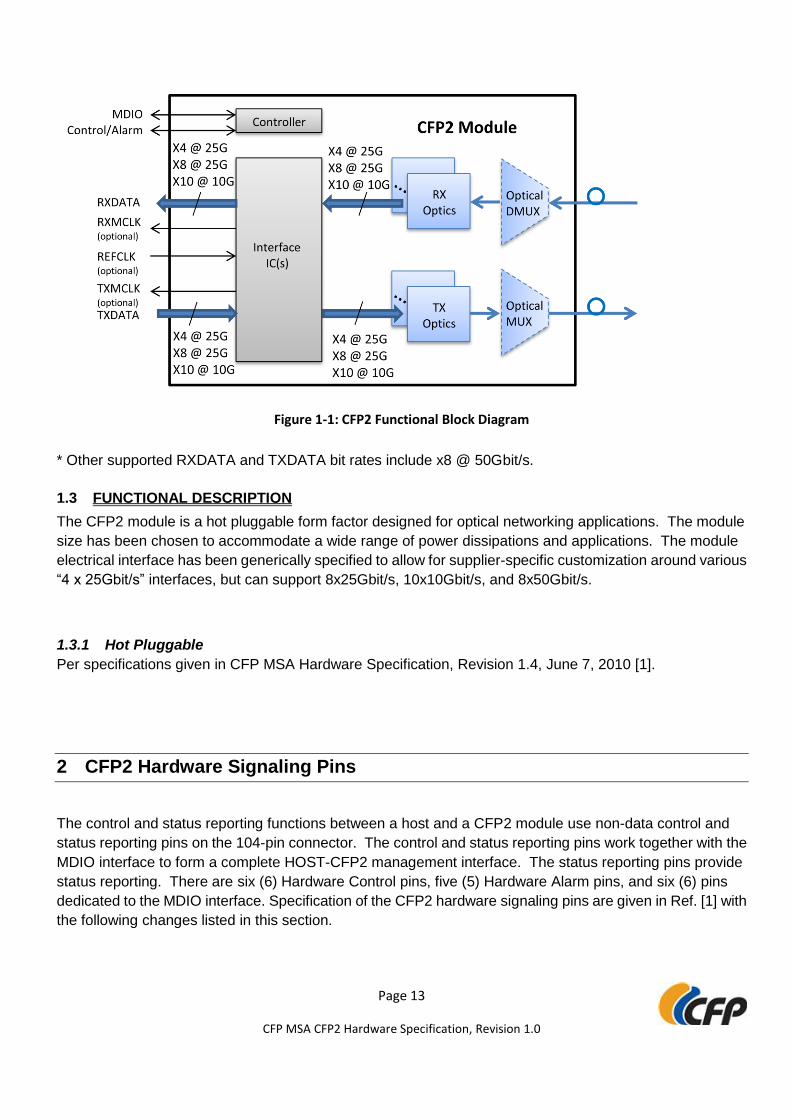
1.2 CFP2 FUNCTIONAL BLOCK DIAGRAM
1 C = 100 in Roman numerals; Centum
Page 13
CFP MSA CFP2 Hardware Specification, Revision 1.0
Figure 1-1: CFP2 Functional Block Diagram
* Other supported RXDATA and TXDATA bit rates include x8 @ 50Gbit/s.
1.3 FUNCTIONAL DESCRIPTION
The CFP2 module is a hot pluggable form factor designed for optical networking applications. The module
size has been chosen to accommodate a wide range of power dissipations and applications. The module
electrical interface has been generically specified to allow for supplier-specific customization around various
“4 x 25Gbit/s” interfaces, but can support 8x25Gbit/s, 10x10Gbit/s, and 8x50Gbit/s.
1.3.1 Hot Pluggable
Per specifications given in CFP MSA Hardware Specification, Revision 1.4, June 7, 2010 [1].
2 CFP2 Hardware Signaling Pins
The control and status reporting functions between a host and a CFP2 module use non-data control and
status reporting pins on the 104-pin connector. The control and status reporting pins work together with the
MDIO interface to form a complete HOST-CFP2 management interface. The status reporting pins provide
status reporting. There are six (6) Hardware Control pins, five (5) Hardware Alarm pins, and six (6) pins
dedicated to the MDIO interface. Specification of the CFP2 hardware signaling pins are given in Ref. [1] with
the following changes listed in this section.
Page 14
CFP MSA CFP2 Hardware Specification, Revision 1.0
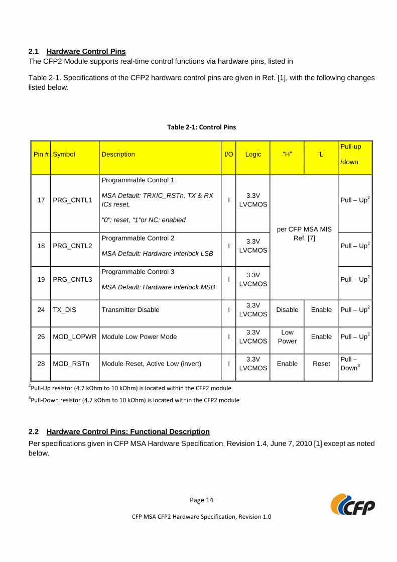
2.1 Hardware Control Pins
The CFP2 Module supports real-time control functions via hardware pins, listed in
Table 2-1. Specifications of the CFP2 hardware control pins are given in Ref. [1], with the following changes
listed below.
Table 2-1: Control Pins
Pin # Symbol Description I/O Logic “H” “L” Pull-up
/down
17 PRG_CNTL1
Programmable Control 1
MSA Default: TRXIC_RSTn, TX & RX
ICs reset,
"0": reset, "1"or NC: enabled
I 3.3V
LVCMOS
per CFP MSA MIS
Ref. [7]
Pull – Up2
18 PRG_CNTL2 Programmable Control 2
MSA Default: Hardware Interlock LSB I
3.3V
LVCMOS Pull – Up
2
19 PRG_CNTL3 Programmable Control 3
MSA Default: Hardware Interlock MSB I
3.3V
LVCMOS Pull – Up
2
24 TX_DIS Transmitter Disable I 3.3V
LVCMOS Disable Enable Pull – Up
2
26 MOD_LOPWR Module Low Power Mode I 3.3V
LVCMOS
Low
Power Enable Pull – Up
2
28 MOD_RSTn Module Reset, Active Low (invert) I 3.3V
LVCMOS Enable Reset
Pull –
Down3
2Pull-Up resistor (4.7 kOhm to 10 kOhm) is located within the CFP2 module
3Pull-Down resistor (4.7 kOhm to 10 kOhm) is located within the CFP2 module
2.2 Hardware Control Pins: Functional Description
Per specifications given in CFP MSA Hardware Specification, Revision 1.4, June 7, 2010 [1] except as noted
below.
Page 15
CFP MSA CFP2 Hardware Specification, Revision 1.0
2.2.1 Programmable Controls (PRG_CNTLs)
2.2.1.1 Hardware Interlock
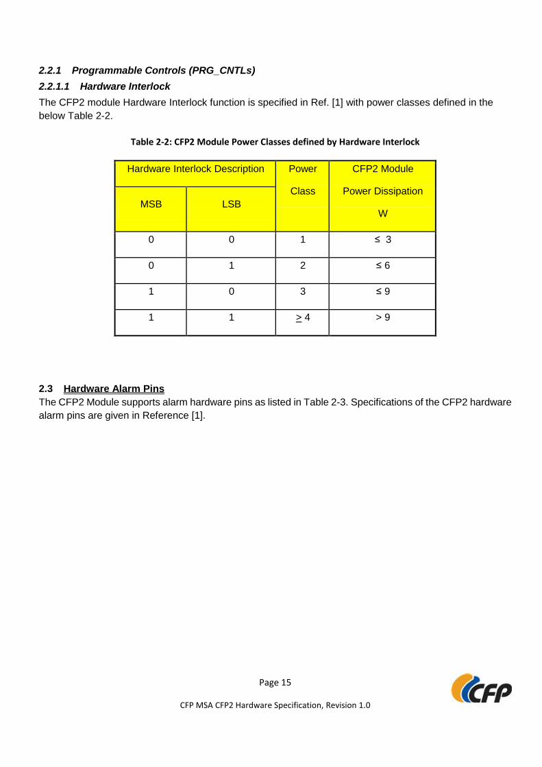
The CFP2 module Hardware Interlock function is specified in Ref. [1] with power classes defined in the
below Table 2-2.
Table 2-2: CFP2 Module Power Classes defined by Hardware Interlock
Hardware Interlock Description Power
Class
CFP2 Module
Power Dissipation
W MSB LSB
0 0 1 ≤ 3
0 1 2 ≤ 6
1 0 3 ≤ 9
1 1 > 4 > 9
2.3 Hardware Alarm Pins
The CFP2 Module supports alarm hardware pins as listed in Table 2-3. Specifications of the CFP2 hardware
alarm pins are given in Reference [1].

Page 16
CFP MSA CFP2 Hardware Specification, Revision 1.0
Table 2-3: Hardware Alarm Pins
Pin
# Symbol Description I/O Logic “H” “L”
Pull-up
/down
20 PRG_ALRM1 Programmable Alarm 1
MSA Default: HIPWR_ON O
3.3V
LVCMOS
Active High
per CFP MSA MIS
Ref. [7]
21 PRG_ALRM2
Programmable Alarm 2
MSA Default: MOD_READY, Ready
state has been reached
O 3.3V
LVCMOS
22 PRG_ALRM3 Programmable Alarm 3
MSA Default: MOD_FAULT O
3.3V
LVCMOS
25 RX_LOS Receiver Loss of Signal O 3.3V
LVCMOS
Loss of
Signal OK
27 MOD_ABS Module Absent O 3.3V
LVCMOS Absent Present
Pull
Down2
2.4 Hardware Alarm Pins: Functional Description
Per specifications given in CFP MSA Hardware Specification, Revision 1.4, June 7, 2010 [1].
2.5 Management Interface Pins
The CFP2 Module supports alarm, control and monitor functions via an MDIO bus. Upon module
initialization, these functions are available. CFP2 MDIO electrical interface consists of six (6) pins including
two (2) pins for MDC and MDIO, three (3) Physical Port Address pins, and the Global Alarm pin. MDC is the
MDIO Clock line driven by the host and MDIO is the bidirectional data line driven by both the host and
module depending upon the data directions. The CFP2 MDIO pins are listed in Table 2-4. Specifications of
the CFP2 hardware management interface pins are given in Reference [1] with the following changes listed
below.
2 Pull-Down resistor (<100 Ohm) is located within the CFP2 module. Pull-up should be located on the host.
Page 17
CFP MSA CFP2 Hardware Specification, Revision 1.0
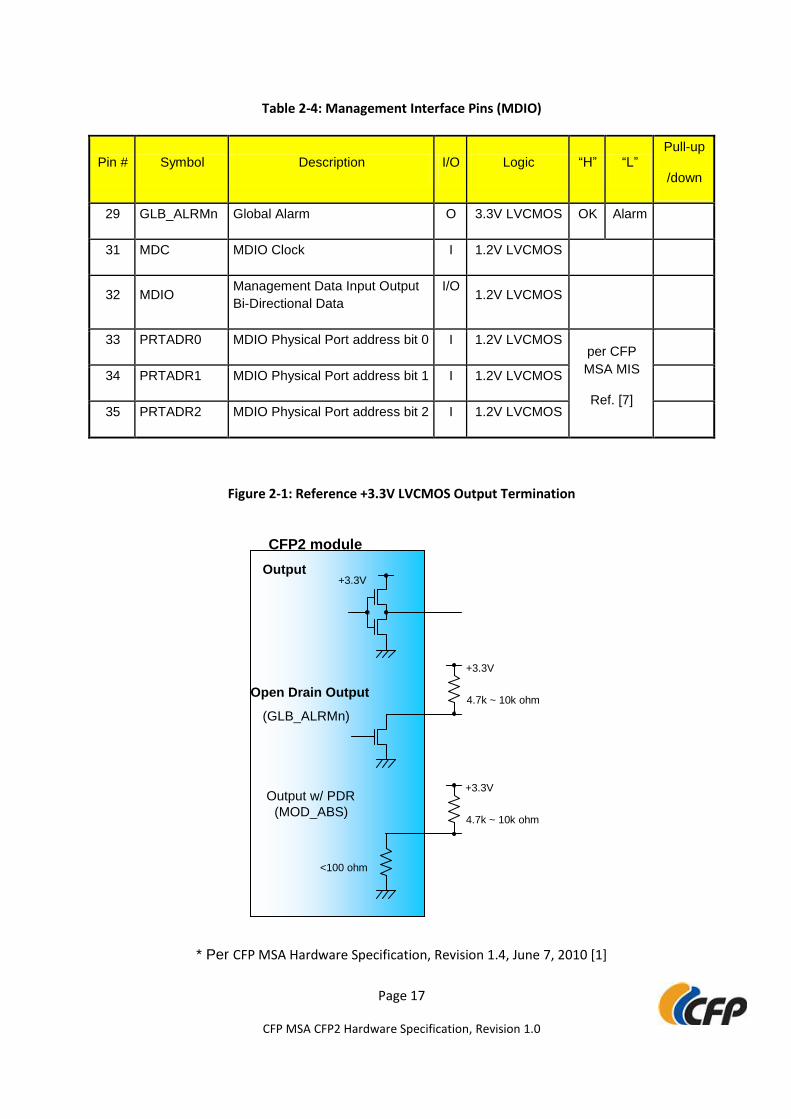
Table 2-4: Management Interface Pins (MDIO)
Pin # Symbol Description I/O Logic “H” “L” Pull-up
/down
29 GLB_ALRMn Global Alarm O 3.3V LVCMOS OK Alarm
31 MDC MDIO Clock I 1.2V LVCMOS
32 MDIO Management Data Input Output
Bi-Directional Data
I/O 1.2V LVCMOS
33 PRTADR0 MDIO Physical Port address bit 0 I 1.2V LVCMOS per CFP
MSA MIS
Ref. [7]
34 PRTADR1 MDIO Physical Port address bit 1 I 1.2V LVCMOS
35 PRTADR2 MDIO Physical Port address bit 2 I 1.2V LVCMOS
Figure 2-1: Reference +3.3V LVCMOS Output Termination
* Per CFP MSA Hardware Specification, Revision 1.4, June 7, 2010 [1]
Output
CFP2 module
Open Drain Output
(GLB_ALRMn)
Output w/ PDR
(MOD_ABS)
4.7k ~ 10k ohm
+3.3V
4.7k ~ 10k ohm
+3.3V
+3.3V
<100 ohm
Page 18
CFP MSA CFP2 Hardware Specification, Revision 1.0
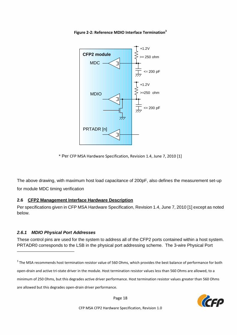
Figure 2-2: Reference MDIO Interface Termination3
* Per CFP MSA Hardware Specification, Revision 1.4, June 7, 2010 [1]
The above drawing, with maximum host load capacitance of 200pF, also defines the measurement set-up
for module MDC timing verification
2.6 CFP2 Management Interface Hardware Description
Per specifications given in CFP MSA Hardware Specification, Revision 1.4, June 7, 2010 [1] except as noted
below.
2.6.1 MDIO Physical Port Addresses
These control pins are used for the system to address all of the CFP2 ports contained within a host system.
PRTADR0 corresponds to the LSB in the physical port addressing scheme. The 3-wire Physical Port
3 The MSA recommends host termination resistor value of 560 Ohms, which provides the best balance of performance for both
open-drain and active tri-state driver in the module. Host termination resistor values less than 560 Ohms are allowed, to a
minimum of 250 Ohms, but this degrades active driver performance. Host termination resistor values greater than 560 Ohms
are allowed but this degrades open-drain driver performance.
+ 1 . 2 V
MDC
CFP2 module
+ 1 . 2 V
MDIO
PRTADR [n]
> = 250 ohm
< = 200 pF
> = 250 ohm
< = 200 pF
Page 19
CFP MSA CFP2 Hardware Specification, Revision 1.0
Address lines are driven by host to set the module Physical Port Address which should match the address
specified in the MDIO Frame. It is recommended that the Physical Port Addresses not be changed while the
CFP2 module is powered on because this will result in unpredictable module behavior.
2.7 Hardware Signaling Pin Electrical Specifications
Per specifications given in CFP MSA Hardware Specification, Revision 1.4, June 7, 2010 [1].
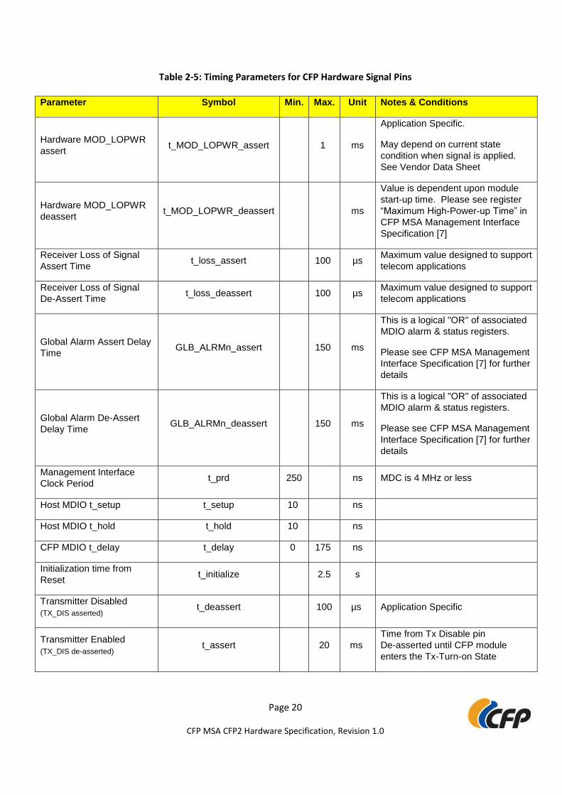
2.8 Hardware Signaling Pin Timing Requirements
Timing requirements for Hardware Signaling Pins can be found in Table 2-5.
Page 20
CFP MSA CFP2 Hardware Specification, Revision 1.0
Table 2-5: Timing Parameters for CFP Hardware Signal Pins
Parameter Symbol Min. Max. Unit Notes & Conditions
Hardware MOD_LOPWR
assert t_MOD_LOPWR_assert 1 ms
Application Specific.
May depend on current state
condition when signal is applied.
See Vendor Data Sheet
Hardware MOD_LOPWR
deassert t_MOD_LOPWR_deassert ms
Value is dependent upon module
start-up time. Please see register
“Maximum High-Power-up Time” in
CFP MSA Management Interface
Specification [7]
Receiver Loss of Signal
Assert Time t_loss_assert 100 µs
Maximum value designed to support
telecom applications
Receiver Loss of Signal
De-Assert Time t_loss_deassert 100 µs
Maximum value designed to support
telecom applications
Global Alarm Assert Delay
Time GLB_ALRMn_assert 150 ms
This is a logical "OR" of associated
MDIO alarm & status registers.
Please see CFP MSA Management
Interface Specification [7] for further
details
Global Alarm De-Assert
Delay Time GLB_ALRMn_deassert 150 ms
This is a logical "OR" of associated
MDIO alarm & status registers.
Please see CFP MSA Management
Interface Specification [7] for further
details
Management Interface
Clock Period t_prd 250 ns MDC is 4 MHz or less
Host MDIO t_setup t_setup 10 ns
Host MDIO t_hold t_hold 10 ns
CFP MDIO t_delay t_delay 0 175 ns
Initialization time from
Reset t_initialize 2.5 s
Transmitter Disabled
(TX_DIS asserted) t_deassert 100 µs Application Specific
Transmitter Enabled
(TX_DIS de-asserted) t_assert 20 ms
Time from Tx Disable pin
De-asserted until CFP module
enters the Tx-Turn-on State
Page 21
CFP MSA CFP2 Hardware Specification, Revision 1.0
3 MODULE MANAGEMENT INTERFACE DESCRIPTION
The CFP2 module utilizes MDIO IEEE Std 802.3TM-2012 clause 45 [8] for its management interface. The
CFP2 MDIO implementation is defined in a separate document entitled, “CFP MSA Management Interface
Specification” [7]. When multiple CFP2 modules are connected via a single bus, a particular CFP2 module
can be selected by using the Physical Port Address pins.
Page 22
CFP MSA CFP2 Hardware Specification, Revision 1.0
4 PERFORMANCE SPECIFICATIONS
4.1 OPERATING ENVIRONMENT
Per specifications given in CFP MSA Hardware Specification, Revision 1.4, June 7, 2010 [1].
4.2 POWER SUPPLIES AND POWER DISSIPATION
4.2.1 Voltage power supply and power dissipation
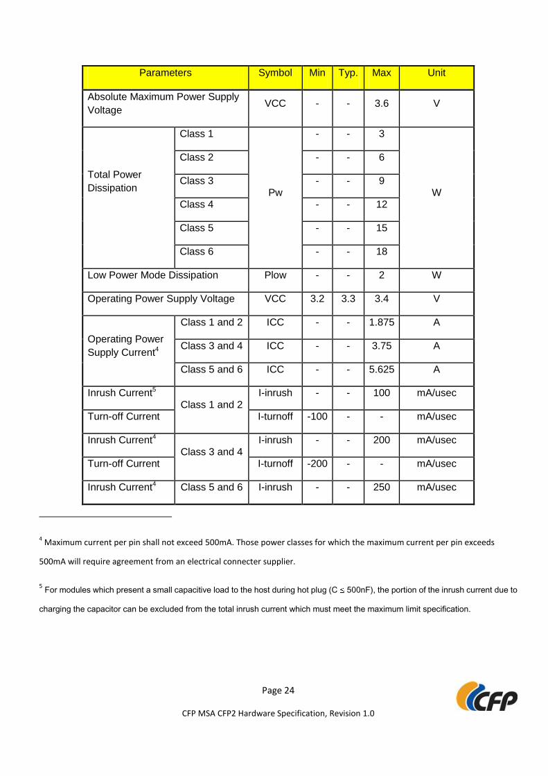
The CFP2 module power supply and maximum power dissipation specifications are defined in Table 4-1.
4.2.2 Inrush current
The inrush current on the 3.3V power supply shall be limited by the CFP2 module to assure a maximum rate
of change defined in Table 4-1.
4.2.3 Turn-off current
The CFP2 module shall limit the turn-off current to assure a maximum rate of change per Table 4-1.
4.2.4 Power Supply Noise Susceptibility
A host system will supply stable power to the module and guarantee that noise & ripple on the power supply
does not exceed that defined in the table. A possible example of a power supply filtering circuit that might be
used on the host system is a PI C-L-C filter. A module will meet all electrical requirements and remain fully
operational in the presence of noise on the 3.3V power supply which is less than that defined in the table 4-1.
The component values of power supply noise filtering circuit, such as the capacitor and inductor, must be
selected such that maximum Inrush and Turn-off current does not cause voltage transients which exceed the
absolute maximum power supply voltage, all specified in Table 4-1.
Page 23
CFP MSA CFP2 Hardware Specification, Revision 1.0
Table 4-1 Voltage power supply
Page 24
CFP MSA CFP2 Hardware Specification, Revision 1.0
Parameters Symbol Min Typ. Max Unit
Absolute Maximum Power Supply
Voltage VCC - - 3.6 V
Total Power
Dissipation
Class 1
Pw
- - 3
W
Class 2 - - 6
Class 3 - - 9
Class 4 - - 12
Class 5 - - 15
Class 6 - - 18
Low Power Mode Dissipation Plow - - 2 W
Operating Power Supply Voltage VCC 3.2 3.3 3.4 V
Operating Power
Supply Current4
Class 1 and 2 ICC - - 1.875 A
Class 3 and 4 ICC - - 3.75 A
Class 5 and 6 ICC - - 5.625 A
Inrush Current5 Class 1 and 2
I-inrush - - 100 mA/usec
Turn-off Current I-turnoff -100 - - mA/usec
Inrush Current4 Class 3 and 4
I-inrush - - 200 mA/usec
Turn-off Current I-turnoff -200 - - mA/usec
Inrush Current4 Class 5 and 6 I-inrush - - 250 mA/usec
4 Maximum current per pin shall not exceed 500mA. Those power classes for which the maximum current per pin exceeds
500mA will require agreement from an electrical connecter supplier.
5 For modules which present a small capacitive load to the host during hot plug (C 500nF), the portion of the inrush current due to
charging the capacitor can be excluded from the total inrush current which must meet the maximum limit specification.
Page 25
CFP MSA CFP2 Hardware Specification, Revision 1.0
Turn-off Current I-turnoff -250 - - mA/usec
Power Supply Noise Vrip - - 2%
3%
DC – 1MHz
1 – 10MHz
4.2.5 Grounding
Per specifications given in CFP MSA Hardware Specification, Revision 1.4, June 7, 2010 [1].
4.3 OPTICAL CHARACTERISTICS
4.3.1 Optical specifications
The CFP2 module will comply with standardized optical specifications such as the optical reaches specified
in IEEE for datacom applications or in ITU-T for telecom applications. Some of the relevant reference
documents are: IEEE Std. 802.3TM-2012[5], Telcordia GR-253, ITU-T G.691, ITU-T G.692, ITU-T G.693, and
ITU-T G.959, ITU-T G.709 [4].
4.4 HIGH SPEED ELECTRICAL CHARACTERISTICS
The CFP2 Module high speed electrical interface supports the following configurations:
1) 4 tx lanes + 4 rx lanes, each at 25 Gbit/s;
2) 8 tx lanes + 8 rx lanes, each at 25 Gbit/s;
3) 10 tx lanes + 10 rx lanes, each at 10 Gbit/s.
Following electrical interfaces may be supported in future.
4) 4 tx lanes + 4 rx lanes, each at 50 Gbit/s;
5) 8 tx lanes + 8 rx lanes, each at 50 Gbit/s;
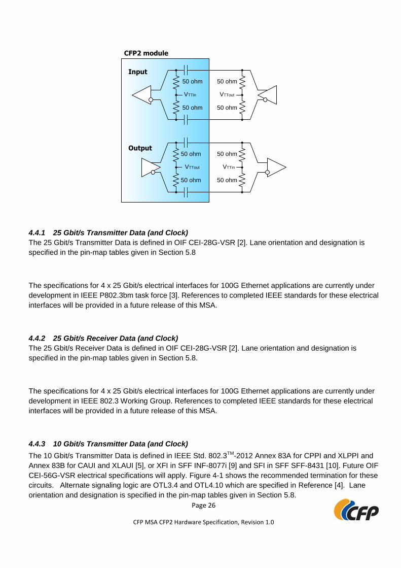
The high speed electrical interface shall be AC-coupled within the CFP2 module as is shown in Figure 4-1.
Figure 4-1: High Speed I/O for Data and Clocks
Page 26
CFP MSA CFP2 Hardware Specification, Revision 1.0
4.4.1 25 Gbit/s Transmitter Data (and Clock)
The 25 Gbit/s Transmitter Data is defined in OIF CEI-28G-VSR [2]. Lane orientation and designation is
specified in the pin-map tables given in Section 5.8
The specifications for 4 x 25 Gbit/s electrical interfaces for 100G Ethernet applications are currently under
development in IEEE P802.3bm task force [3]. References to completed IEEE standards for these electrical
interfaces will be provided in a future release of this MSA.
4.4.2 25 Gbit/s Receiver Data (and Clock)
The 25 Gbit/s Receiver Data is defined in OIF CEI-28G-VSR [2]. Lane orientation and designation is
specified in the pin-map tables given in Section 5.8.
The specifications for 4 x 25 Gbit/s electrical interfaces for 100G Ethernet applications are currently under
development in IEEE 802.3 Working Group. References to completed IEEE standards for these electrical
interfaces will be provided in a future release of this MSA.
4.4.3 10 Gbit/s Transmitter Data (and Clock)
The 10 Gbit/s Transmitter Data is defined in IEEE Std. 802.3TM-2012 Annex 83A for CPPI and XLPPI and
Annex 83B for CAUI and XLAUI [5], or XFI in SFF INF-8077i [9] and SFI in SFF SFF-8431 [10]. Future OIF
CEI-56G-VSR electrical specifications will apply. Figure 4-1 shows the recommended termination for these
circuits. Alternate signaling logic are OTL3.4 and OTL4.10 which are specified in Reference [4]. Lane
orientation and designation is specified in the pin-map tables given in Section 5.8.
Input
CFP2 module
50 ohm
50 ohm
VTTout
50 ohm
50 ohm
VTTin
50 ohm
50 ohm
VTTout
50 ohm
50 ohm
VTTin
Output
Page 27
CFP MSA CFP2 Hardware Specification, Revision 1.0
4.4.4 10 Gbit/s Receiver Data (and Clock)
The 10 Gbit/s Transmitter Data is defined in IEEE Std. 802.3TM-2012 Annex 83A for CPPI and XLPPI and
Annex 83B for CAUI and XLAUI [5], or XFI in SFF INF-8077i [9] and SFI in SFF SFF-8431 [10]. Future OIF
CEI-56G-VSR electrical specifications will apply. Figure 4-1 shows the recommended termination for these
circuits. Alternate signaling logic are OTL3.4 and OTL4.10 which are specified in Reference [4]. Lane
orientation and designation is specified in the pin-map tables given in Section 5.8.
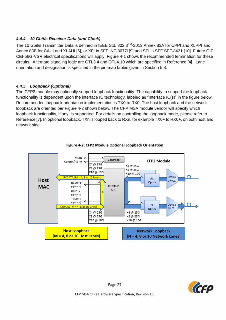
4.4.5 Loopback (Optional)
The CFP2 module may optionally support loopback functionality. The capability to support the loopback
functionality is dependent upon the interface IC technology, labeled as “Interface IC(s)” in the figure below.
Recommended loopback orientation implementation is TX0 to RX0. The host loopback and the network
loopback are oriented per Figure 4-2 shown below. The CFP MSA module vendor will specify which
loopback functionality, if any, is supported. For details on controlling the loopback mode, please refer to
Reference [7]. In optional loopback, TXn is looped back to RXn, for example TX0+ to RX0+, on both host and
network side.
Figure 4-2: CFP2 Module Optional Loopback Orientation
Page 28
CFP MSA CFP2 Hardware Specification, Revision 1.0
4.4.6 Reference Clock (Option)
For M x 25 Gbit/s host electrical interface applications, the host may optionally supply a reference clock
(REFCLK) at 1/160 electrical lane rate. The CFP2 module may optionally use the 1/160 reference clock or
the 1/32 network lane rate clock recovered from the receiver path for transmitter path retiming, for example
for Ethernet applications.
The host shall optionally supply a reference clock (REFCLK) at 1/40 electrical lane rate for M x 25 Gbit/s
applications. The CFP2 module may optionally use the 1/40 reference clock for transmitter path retiming, for
example for Telecom applications.
For M x 10 Gbit/s host electrical interface applications, the host may optionally supply a reference clock
(REFCLK) at 1/64 electrical lane rate. The CFP2 module may optionally use the 1/64 reference clock for
transmitter path retiming, for example for Ethernet applications.
The host may optionally supply a reference clock (REFCLK) at 1/16 electrical lane rate for M x 10 Gbit/s
applications. The CFP2 module may optionally use the 1/16 reference clock for transmitter path retiming, for
example for Telecom applications.
When provided, the REFCLK shall be CML differential AC-coupled and terminated within the CFP2 module
as shown in Figure 4-1. There is no required phase relationship between the data lanes and the reference
clock, but the clock frequency shall not deviate more than specified in Table 4-2. For detailed clock
characteristics please refer to the below table.
Table 4-2: Optional Reference Clock Characteristics
Min. Typ. Max. Unit Notes
Impedance Zd 80 100 120 Ω
Frequency See Table 4-4: CFP2 Module Clocking Signals
Frequency Stability f
-100 100
ppm
For Ethernet applications;
-20 20 For Telecom applications
Output Differential
Voltage VDIFF 400 1200 mV Peak to Peak Differential
Page 29
CFP MSA CFP2 Hardware Specification, Revision 1.0
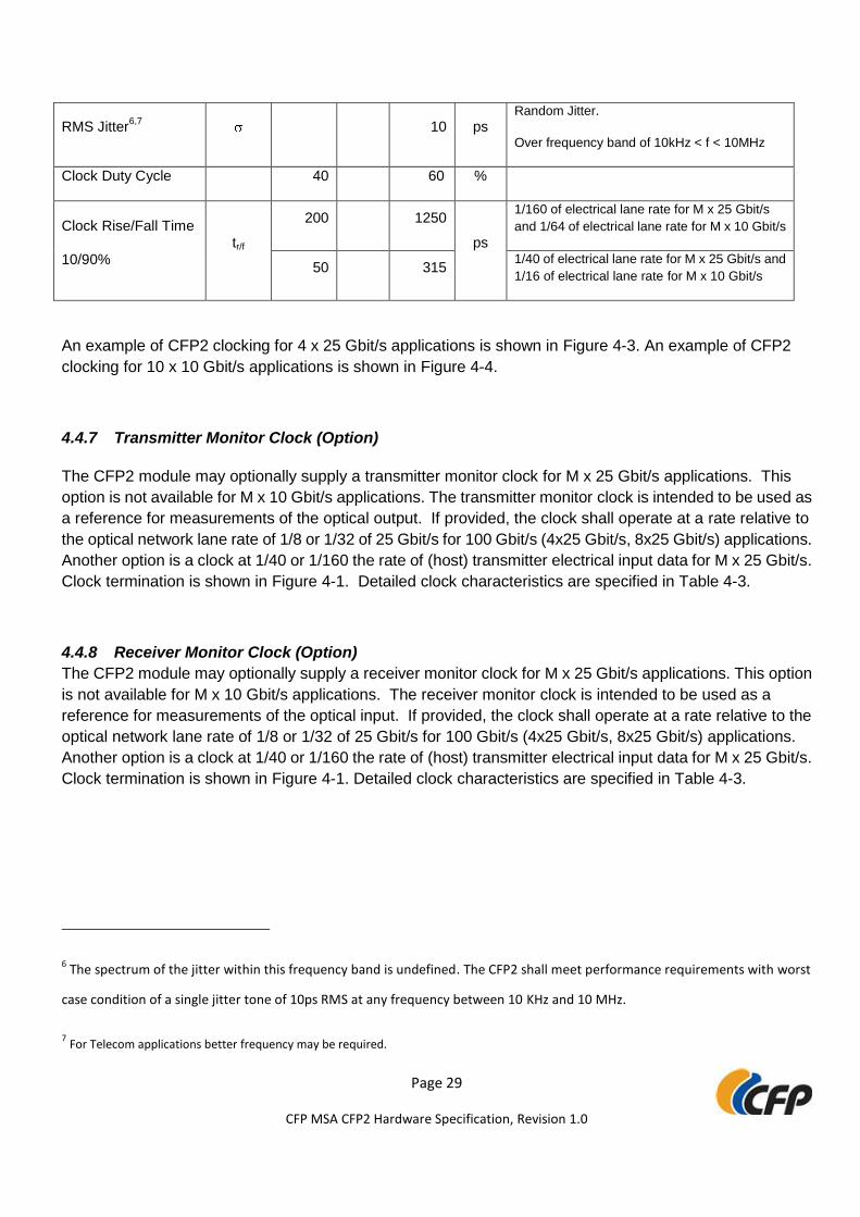
RMS Jitter6,7
10 ps Random Jitter.
Over frequency band of 10kHz < f < 10MHz
Clock Duty Cycle 40 60 %
Clock Rise/Fall Time
10/90% tr/f
200 1250
ps
1/160 of electrical lane rate for M x 25 Gbit/s
and 1/64 of electrical lane rate for M x 10 Gbit/s
50 315 1/40 of electrical lane rate for M x 25 Gbit/s and
1/16 of electrical lane rate for M x 10 Gbit/s
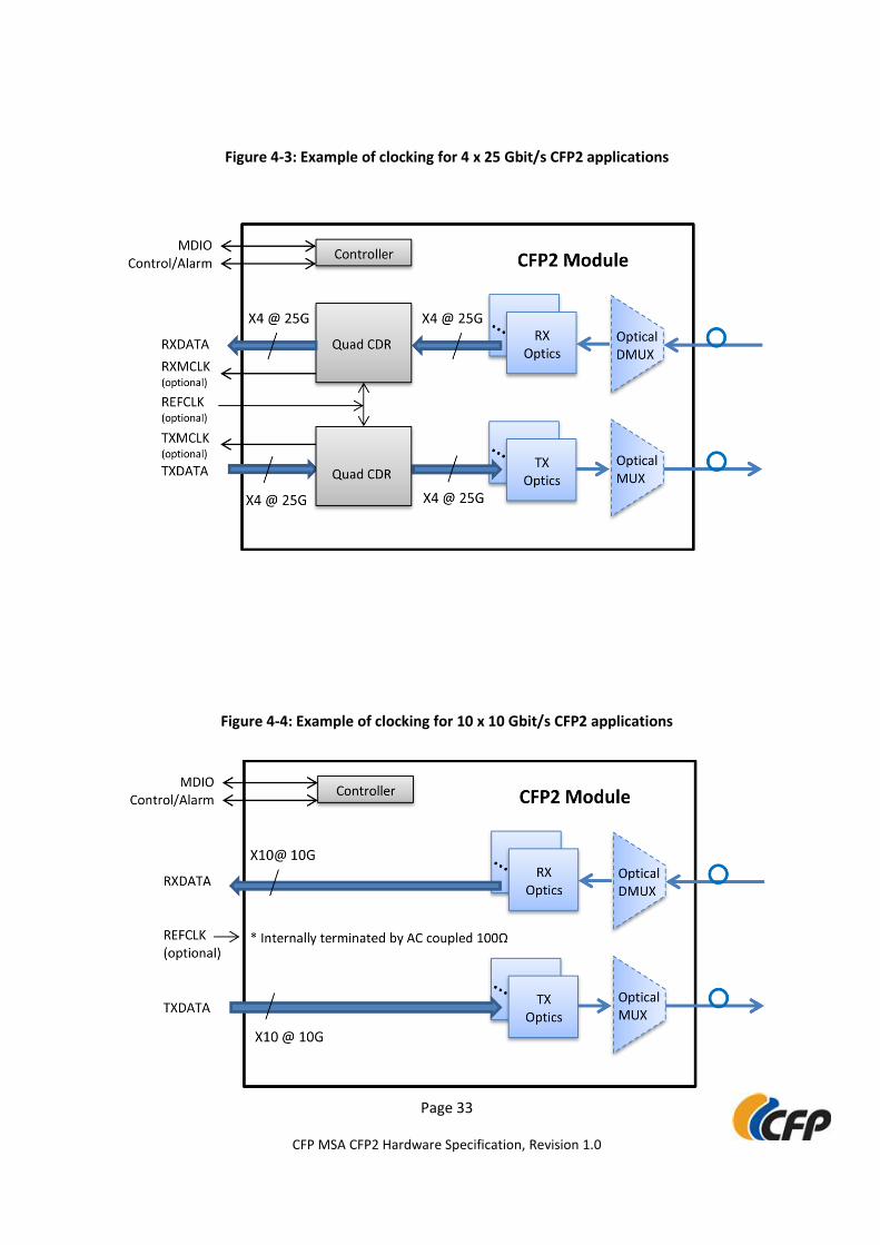
An example of CFP2 clocking for 4 x 25 Gbit/s applications is shown in Figure 4-3. An example of CFP2
clocking for 10 x 10 Gbit/s applications is shown in Figure 4-4.
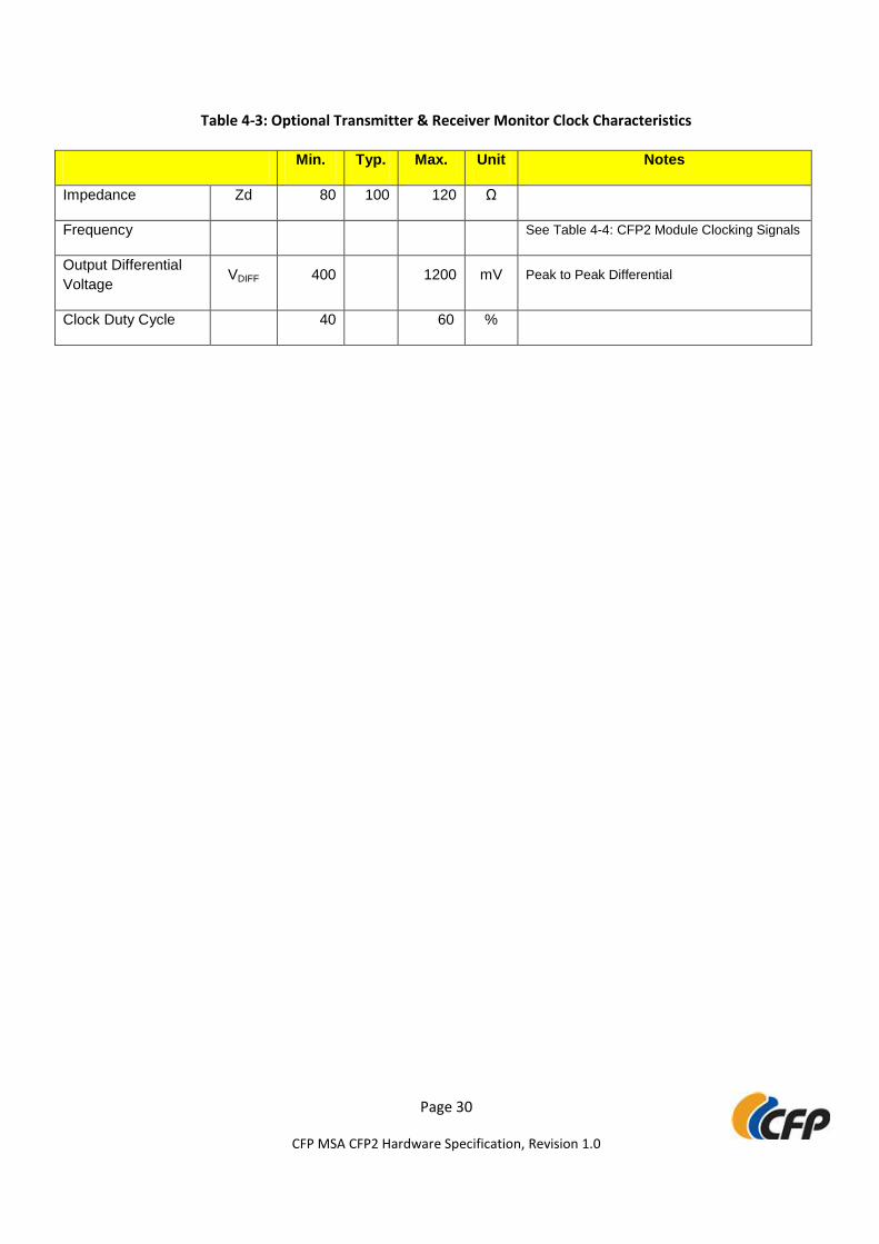
4.4.7 Transmitter Monitor Clock (Option)
The CFP2 module may optionally supply a transmitter monitor clock for M x 25 Gbit/s applications. This
option is not available for M x 10 Gbit/s applications. The transmitter monitor clock is intended to be used as
a reference for measurements of the optical output. If provided, the clock shall operate at a rate relative to
the optical network lane rate of 1/8 or 1/32 of 25 Gbit/s for 100 Gbit/s (4x25 Gbit/s, 8x25 Gbit/s) applications.
Another option is a clock at 1/40 or 1/160 the rate of (host) transmitter electrical input data for M x 25 Gbit/s.
Clock termination is shown in Figure 4-1. Detailed clock characteristics are specified in Table 4-3.
4.4.8 Receiver Monitor Clock (Option)
The CFP2 module may optionally supply a receiver monitor clock for M x 25 Gbit/s applications. This option
is not available for M x 10 Gbit/s applications. The receiver monitor clock is intended to be used as a
reference for measurements of the optical input. If provided, the clock shall operate at a rate relative to the
optical network lane rate of 1/8 or 1/32 of 25 Gbit/s for 100 Gbit/s (4x25 Gbit/s, 8x25 Gbit/s) applications.
Another option is a clock at 1/40 or 1/160 the rate of (host) transmitter electrical input data for M x 25 Gbit/s.
Clock termination is shown in Figure 4-1. Detailed clock characteristics are specified in Table 4-3.
6 The spectrum of the jitter within this frequency band is undefined. The CFP2 shall meet performance requirements with worst
case condition of a single jitter tone of 10ps RMS at any frequency between 10 KHz and 10 MHz.
7 For Telecom applications better frequency may be required.
Page 30
CFP MSA CFP2 Hardware Specification, Revision 1.0
Table 4-3: Optional Transmitter & Receiver Monitor Clock Characteristics
Min. Typ. Max. Unit Notes
Impedance Zd 80 100 120 Ω
Frequency See Table 4-4: CFP2 Module Clocking Signals
Output Differential
Voltage VDIFF 400 1200 mV Peak to Peak Differential
Clock Duty Cycle 40 60 %
Page 31
CFP MSA CFP2 Hardware Specification, Revision 1.0
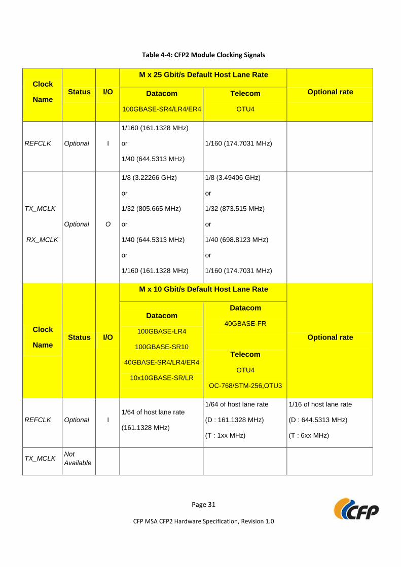
Table 4-4: CFP2 Module Clocking Signals
Clock
Name Status I/O
M x 25 Gbit/s Default Host Lane Rate
Optional rate Datacom
100GBASE-SR4/LR4/ER4
Telecom
OTU4
REFCLK Optional I
1/160 (161.1328 MHz)
or
1/40 (644.5313 MHz)
1/160 (174.7031 MHz)
TX_MCLK
RX_MCLK
Optional O
1/8 (3.22266 GHz)
or
1/32 (805.665 MHz)
or
1/40 (644.5313 MHz)
or
1/160 (161.1328 MHz)
1/8 (3.49406 GHz)
or
1/32 (873.515 MHz)
or
1/40 (698.8123 MHz)
or
1/160 (174.7031 MHz)
Clock
Name Status I/O
M x 10 Gbit/s Default Host Lane Rate
Optional rate
Datacom
100GBASE-LR4
100GBASE-SR10
40GBASE-SR4/LR4/ER4
10x10GBASE-SR/LR
Datacom
40GBASE-FR
Telecom
OTU4
OC-768/STM-256,OTU3
REFCLK Optional I 1/64 of host lane rate
(161.1328 MHz)
1/64 of host lane rate
(D : 161.1328 MHz)
(T : 1xx MHz)
1/16 of host lane rate
(D : 644.5313 MHz)
(T : 6xx MHz)
TX_MCLK Not
Available
Page 32
CFP MSA CFP2 Hardware Specification, Revision 1.0
RX_MCLK Not
Available
Note: Multi-protocol modules are recommended to adopt the clock rate used in Telecom applications.
Page 33
CFP MSA CFP2 Hardware Specification, Revision 1.0
Figure 4-3: Example of clocking for 4 x 25 Gbit/s CFP2 applications
Figure 4-4: Example of clocking for 10 x 10 Gbit/s CFP2 applications

Page 34
CFP MSA CFP2 Hardware Specification, Revision 1.0
Page 35
CFP MSA CFP2 Hardware Specification, Revision 1.0
5 MECHANICAL SPECIFICATIONS
5.1 Mechanical Overview
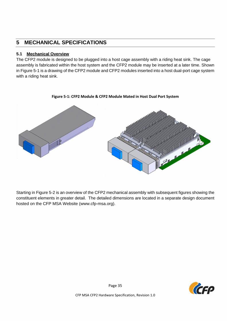
The CFP2 module is designed to be plugged into a host cage assembly with a riding heat sink. The cage
assembly is fabricated within the host system and the CFP2 module may be inserted at a later time. Shown
in Figure 5-1 is a drawing of the CFP2 module and CFP2 modules inserted into a host dual-port cage system
with a riding heat sink.
Figure 5-1: CFP2 Module & CFP2 Module Mated in Host Dual Port System
Starting in Figure 5-2 is an overview of the CFP2 mechanical assembly with subsequent figures showing the
constituent elements in greater detail. The detailed dimensions are located in a separate design document
hosted on the CFP MSA Website (www.cfp-msa.org).
Page 36
CFP MSA CFP2 Hardware Specification, Revision 1.0
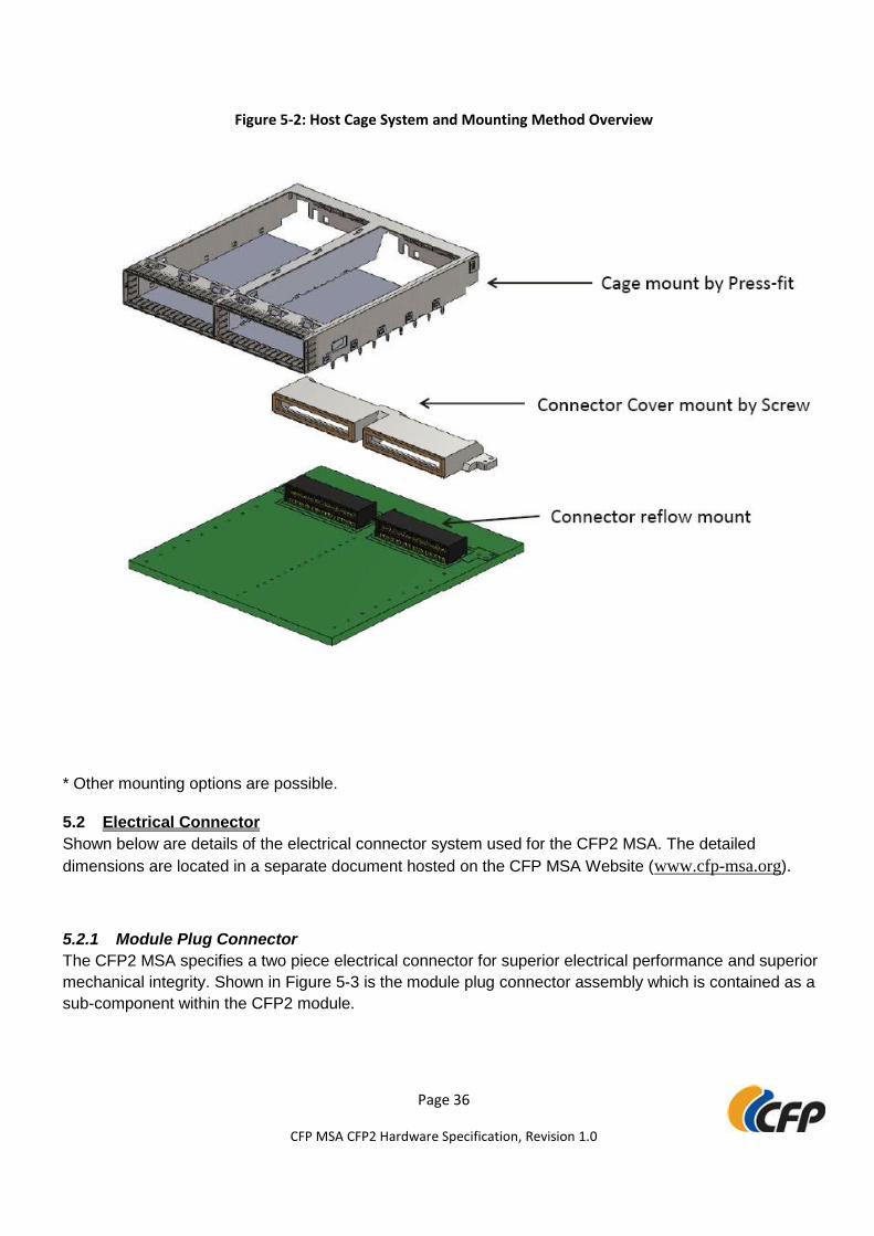
Figure 5-2: Host Cage System and Mounting Method Overview
* Other mounting options are possible.
5.2 Electrical Connector
Shown below are details of the electrical connector system used for the CFP2 MSA. The detailed
dimensions are located in a separate document hosted on the CFP MSA Website (www.cfp-msa.org).
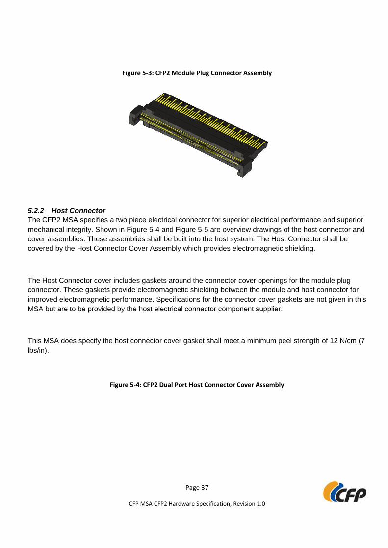
5.2.1 Module Plug Connector
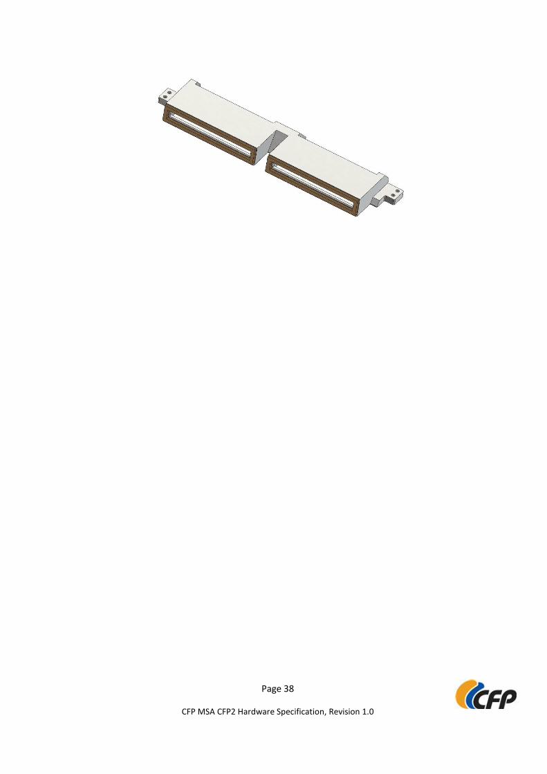
The CFP2 MSA specifies a two piece electrical connector for superior electrical performance and superior
mechanical integrity. Shown in Figure 5-3 is the module plug connector assembly which is contained as a
sub-component within the CFP2 module.
Page 37
CFP MSA CFP2 Hardware Specification, Revision 1.0
Figure 5-3: CFP2 Module Plug Connector Assembly
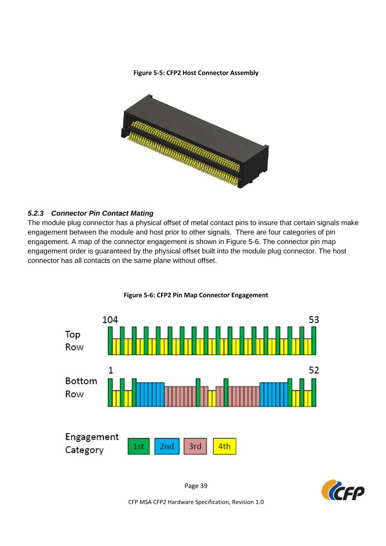
5.2.2 Host Connector
The CFP2 MSA specifies a two piece electrical connector for superior electrical performance and superior
mechanical integrity. Shown in Figure 5-4 and Figure 5-5 are overview drawings of the host connector and
cover assemblies. These assemblies shall be built into the host system. The Host Connector shall be
covered by the Host Connector Cover Assembly which provides electromagnetic shielding.
The Host Connector cover includes gaskets around the connector cover openings for the module plug
connector. These gaskets provide electromagnetic shielding between the module and host connector for
improved electromagnetic performance. Specifications for the connector cover gaskets are not given in this
MSA but are to be provided by the host electrical connector component supplier.
This MSA does specify the host connector cover gasket shall meet a minimum peel strength of 12 N/cm (7
lbs/in).
Figure 5-4: CFP2 Dual Port Host Connector Cover Assembly
Page 38
CFP MSA CFP2 Hardware Specification, Revision 1.0
Page 39
CFP MSA CFP2 Hardware Specification, Revision 1.0
Figure 5-5: CFP2 Host Connector Assembly
5.2.3 Connector Pin Contact Mating
The module plug connector has a physical offset of metal contact pins to insure that certain signals make
engagement between the module and host prior to other signals. There are four categories of pin
engagement. A map of the connector engagement is shown in Figure 5-6. The connector pin map
engagement order is guaranteed by the physical offset built into the module plug connector. The host
connector has all contacts on the same plane without offset.
Figure 5-6: CFP2 Pin Map Connector Engagement

Page 40
CFP MSA CFP2 Hardware Specification, Revision 1.0
Page 41
CFP MSA CFP2 Hardware Specification, Revision 1.0
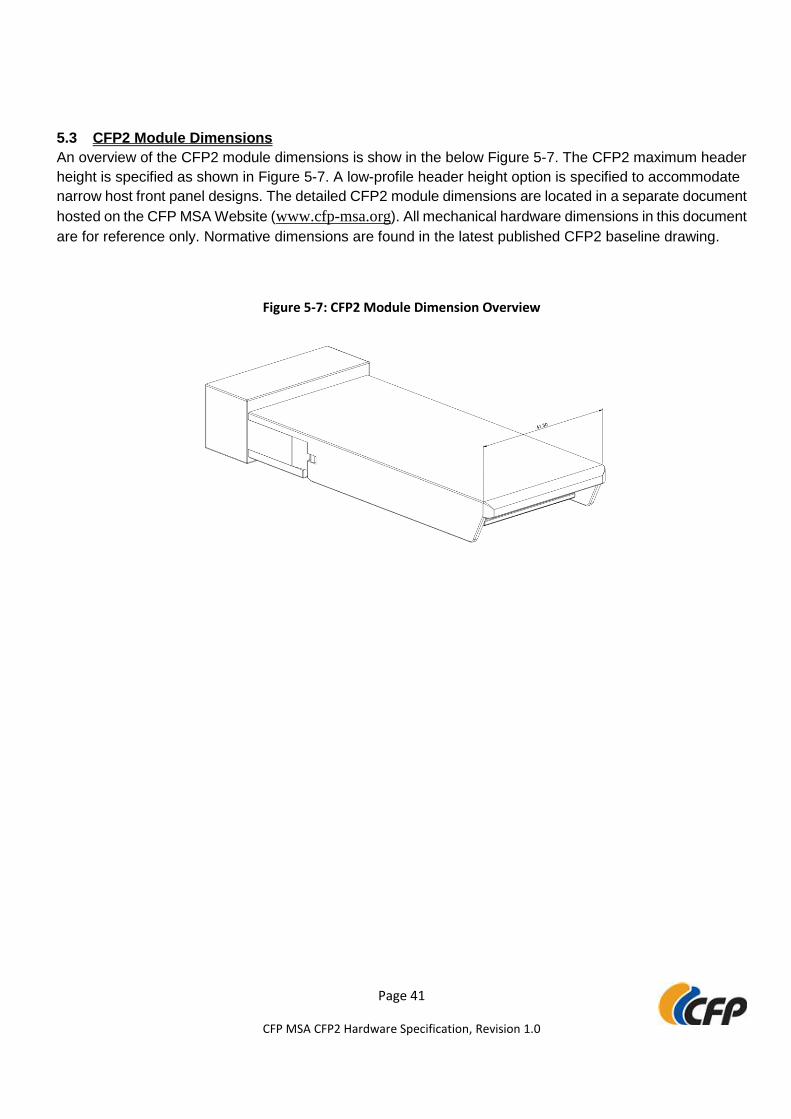
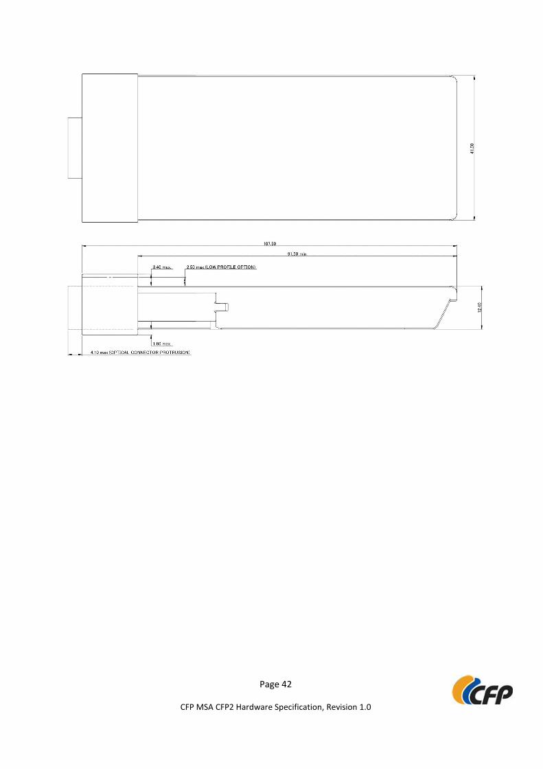
5.3 CFP2 Module Dimensions
An overview of the CFP2 module dimensions is show in the below Figure 5-7. The CFP2 maximum header
height is specified as shown in Figure 5-7. A low-profile header height option is specified to accommodate
narrow host front panel designs. The detailed CFP2 module dimensions are located in a separate document
hosted on the CFP MSA Website (www.cfp-msa.org). All mechanical hardware dimensions in this document
are for reference only. Normative dimensions are found in the latest published CFP2 baseline drawing.
Figure 5-7: CFP2 Module Dimension Overview
Page 42
CFP MSA CFP2 Hardware Specification, Revision 1.0
Page 43
CFP MSA CFP2 Hardware Specification, Revision 1.0
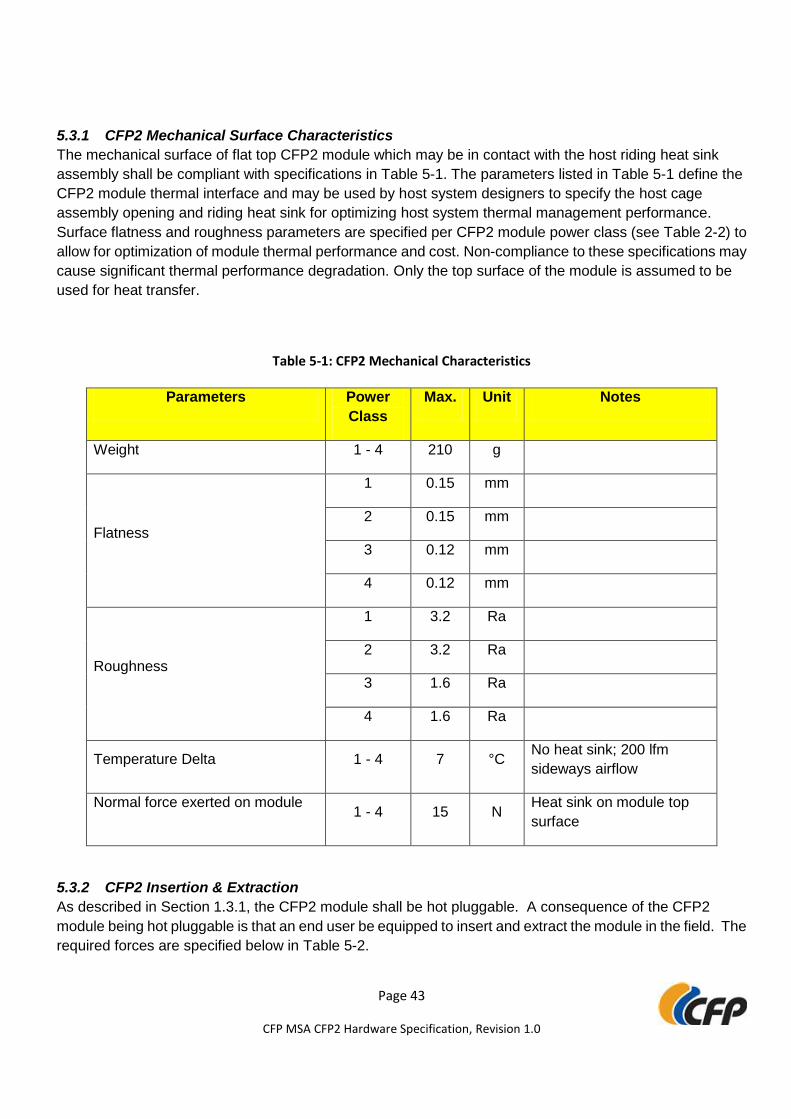
5.3.1 CFP2 Mechanical Surface Characteristics
The mechanical surface of flat top CFP2 module which may be in contact with the host riding heat sink
assembly shall be compliant with specifications in Table 5-1. The parameters listed in Table 5-1 define the
CFP2 module thermal interface and may be used by host system designers to specify the host cage
assembly opening and riding heat sink for optimizing host system thermal management performance.
Surface flatness and roughness parameters are specified per CFP2 module power class (see Table 2-2) to
allow for optimization of module thermal performance and cost. Non-compliance to these specifications may
cause significant thermal performance degradation. Only the top surface of the module is assumed to be
used for heat transfer.
Table 5-1: CFP2 Mechanical Characteristics
Parameters Power
Class
Max. Unit Notes
Weight 1 - 4 210 g
Flatness
1 0.15 mm
2 0.15 mm
3 0.12 mm
4 0.12 mm
Roughness
1 3.2 Ra
2 3.2 Ra
3 1.6 Ra
4 1.6 Ra
Temperature Delta 1 - 4 7 °C No heat sink; 200 lfm
sideways airflow
Normal force exerted on module 1 - 4 15 N
Heat sink on module top
surface
5.3.2 CFP2 Insertion & Extraction
As described in Section 1.3.1, the CFP2 module shall be hot pluggable. A consequence of the CFP2
module being hot pluggable is that an end user be equipped to insert and extract the module in the field. The
required forces are specified below in Table 5-2.
Page 44
CFP MSA CFP2 Hardware Specification, Revision 1.0
Table 5-2: CFP2 Module Insertion, Extraction Forces
Max. Unit Notes
Maximum Insertion Force 80 N Without Heat Sink
Maximum Extraction Force 50 N Without Heat Sink
Minimum Module Retention Force 90 N No damage to module below 90 N
Minimum Cage Retention Force 180 N No damage to cage latch below 180 N
Minimum rating for host/module connector insertion/extraction is 200 cycles.
* Typical increase in those forces by adding heat sink is below 5N.
5.4 Host System Dimensions
The detailed CFP2 host system dimensions including host board layout are located in a separate document
hosted on the CFP MSA Website (www.cfp-msa.org).
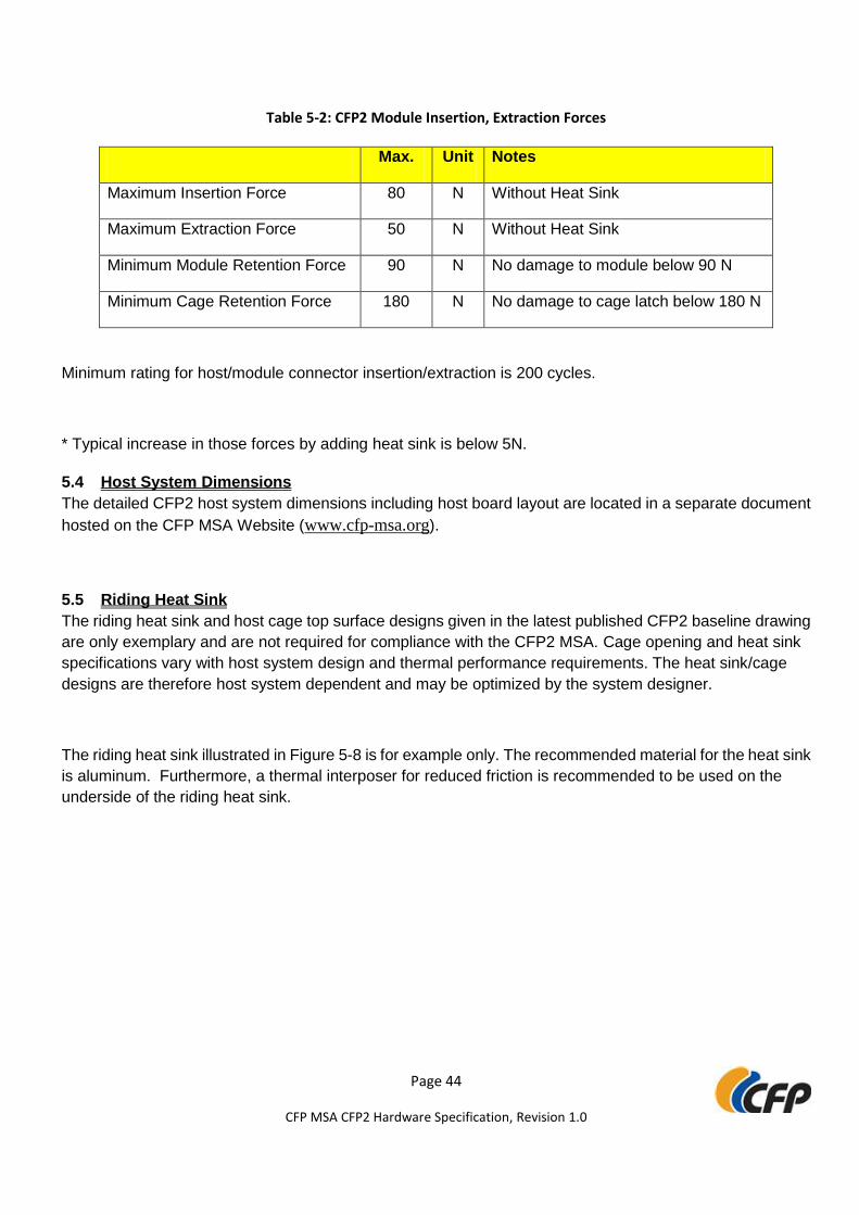
5.5 Riding Heat Sink
The riding heat sink and host cage top surface designs given in the latest published CFP2 baseline drawing
are only exemplary and are not required for compliance with the CFP2 MSA. Cage opening and heat sink
specifications vary with host system design and thermal performance requirements. The heat sink/cage
designs are therefore host system dependent and may be optimized by the system designer.
The riding heat sink illustrated in Figure 5-8 is for example only. The recommended material for the heat sink
is aluminum. Furthermore, a thermal interposer for reduced friction is recommended to be used on the
underside of the riding heat sink.
Page 45
CFP MSA CFP2 Hardware Specification, Revision 1.0
Figure 5-8: Riding Heat Sink
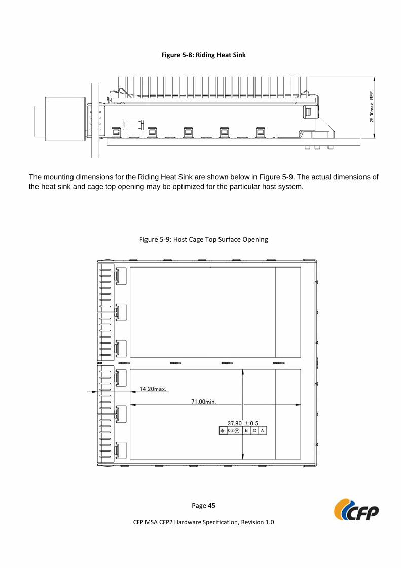
The mounting dimensions for the Riding Heat Sink are shown below in Figure 5-9. The actual dimensions of
the heat sink and cage top opening may be optimized for the particular host system.
Figure 5-9: Host Cage Top Surface Opening

Page 46
CFP MSA CFP2 Hardware Specification, Revision 1.0
Page 47
CFP MSA CFP2 Hardware Specification, Revision 1.0
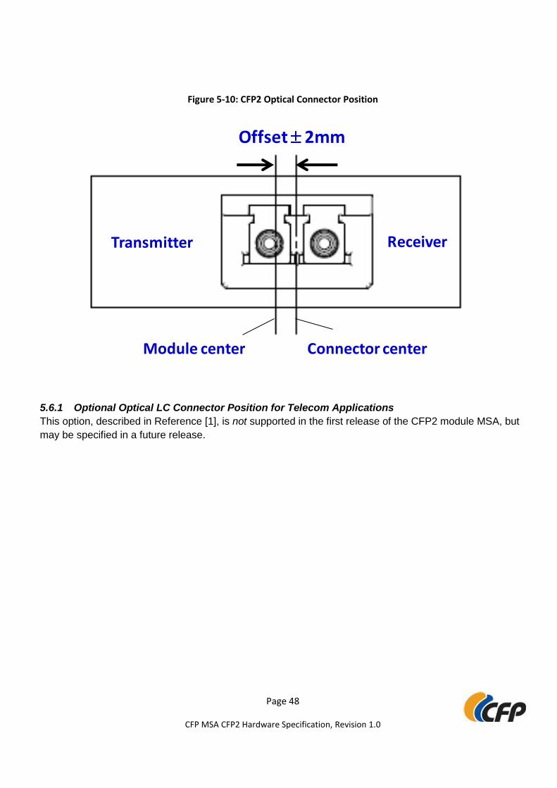
5.6 Optical Connectors
The CFP2 module shall support LC, MTP12 and MTP24 optical connector types, as listed in Table 5-3. The
optical connectors are positioned in the CFP2 module as illustrated in Figure 5-10. The optical connector is
centered in position along the X-axis (module width) with an offset tolerance of ±0.5mm. The position of the
optical connector in the Y and Z axes shall be specified by the CFP2 module manufacturer.
Table 5-3: Optical Connectors8
Pin # Category Reference Number
LC Connector TBA TBA
MPO12 Connector TBA TBA
MPO24 Connector TBA TBA
8 Other optical connectors may be supported
Page 48
CFP MSA CFP2 Hardware Specification, Revision 1.0
Figure 5-10: CFP2 Optical Connector Position
5.6.1 Optional Optical LC Connector Position for Telecom Applications
This option, described in Reference [1], is not supported in the first release of the CFP2 module MSA, but
may be specified in a future release.
Transmitter Receiver
Offset 2mm
Module center Connector center
Page 49
CFP MSA CFP2 Hardware Specification, Revision 1.0
5.7 Electrical Connectors
CFP2 host electrical connector supplier information will be added to Table 5-4 in a future release of this
MSA.
Table 5-4 CFP2 Host Connector Assembly
Part Number Supplier Part Name
TBA TBA Cage
TBA TBA Host Connector Cover Assembly
TBA TBA Host Connector
5.8 Pin Assignment
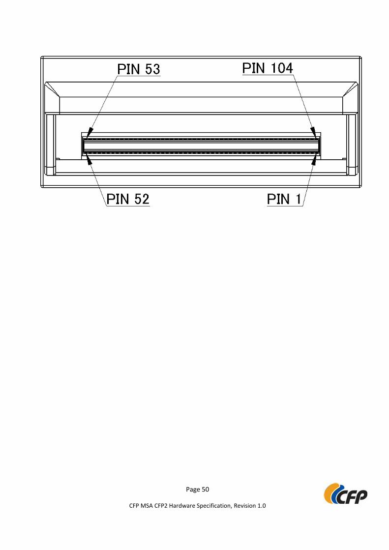
The CFP2 connector has 104 pins which are arranged in Top and Bottom rows. The CFP2 connector
supports the following configurations:
a) Four (4) 25Gbit/s TX lanes plus four 25Gbit/s RX lanes;
b) Eight (8) 25Gbit/s TX lanes plus eight 25Gbit/s RX lanes;
c) Ten (10) 10Gbit/s TX lanes plus ten 10Gbit/s RX lanes.
The CFP2 connector top row and bottom row pin assignments for the N x 25Gbit/s and the 10 x 10Gbit/s
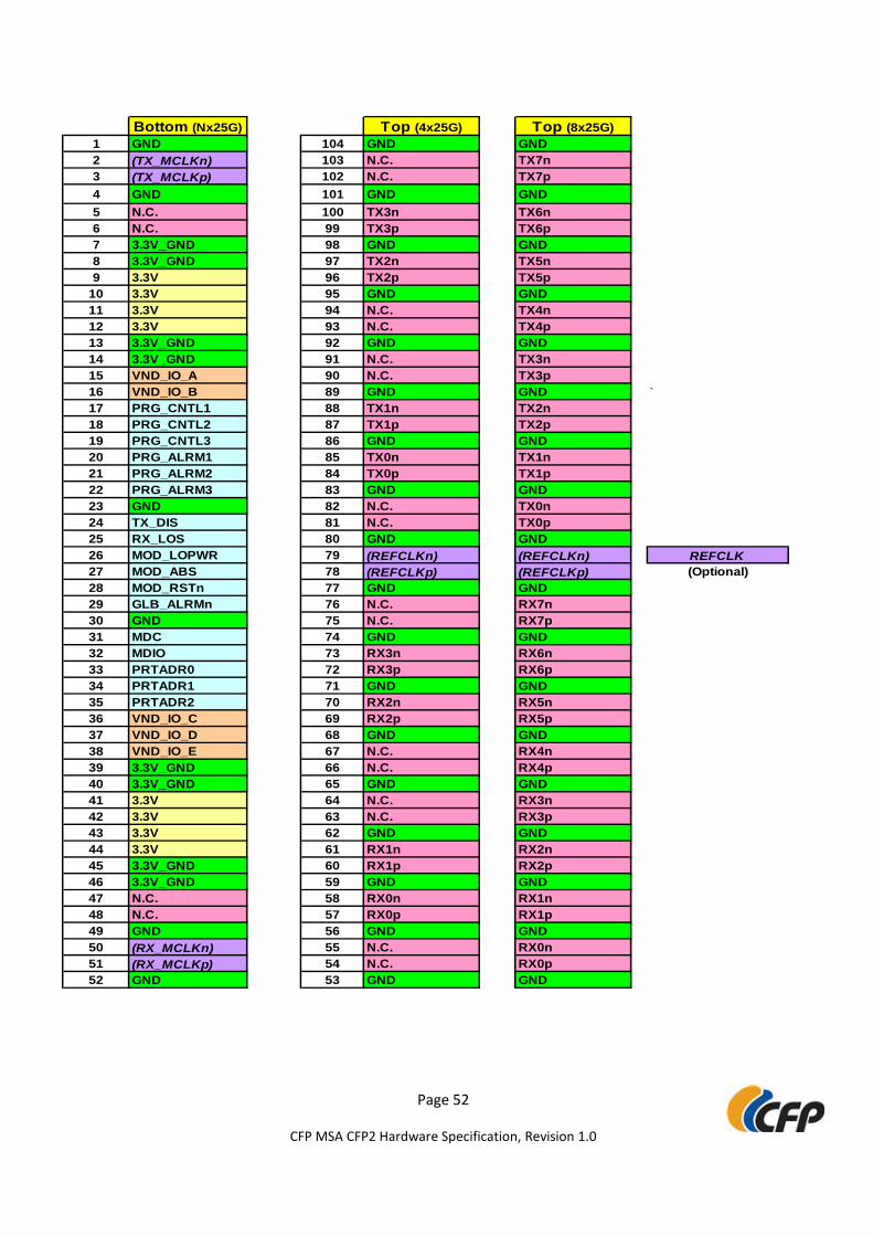
configurations are illustrated in Table 5- and Table 5-6, respectively. Detailed description of the bottom row pins 1
through pin 52 are given in Table 5-7 and Table 5-8. Note the REFCLK pins are located on the top row along with
the high-speed TX and RX data pins. A single-ended REFCLK is an option. The CFP2 connector pin map orientation is
shown in Figure 5-11.
Figure 5-11: CFP2 Connector Pin Map Orientation
Page 50
CFP MSA CFP2 Hardware Specification, Revision 1.0
Page 51
CFP MSA CFP2 Hardware Specification, Revision 1.0
Table 5-5: CFP2 N x 25 Gbit/s Pin-Map
Pin view from top ==> Host
Page 52
CFP MSA CFP2 Hardware Specification, Revision 1.0
Bottom (Nx25G) Top (4x25G) Top (8x25G)
1 GND 104 GND GND
2 (TX_MCLKn) 103 N.C. TX7n
3 (TX_MCLKp) 102 N.C. TX7p
4 GND 101 GND GND
5 N.C. 100 TX3n TX6n
6 N.C. 99 TX3p TX6p
7 3.3V_GND 98 GND GND
8 3.3V_GND 97 TX2n TX5n
9 3.3V 96 TX2p TX5p
10 3.3V 95 GND GND
11 3.3V 94 N.C. TX4n
12 3.3V 93 N.C. TX4p
13 3.3V_GND 92 GND GND
14 3.3V_GND 91 N.C. TX3n
15 VND_IO_A 90 N.C. TX3p
16 VND_IO_B 89 GND GND `
17 PRG_CNTL1 88 TX1n TX2n
18 PRG_CNTL2 87 TX1p TX2p
19 PRG_CNTL3 86 GND GND
20 PRG_ALRM1 85 TX0n TX1n
21 PRG_ALRM2 84 TX0p TX1p
22 PRG_ALRM3 83 GND GND
23 GND 82 N.C. TX0n
24 TX_DIS 81 N.C. TX0p
25 RX_LOS 80 GND GND
26 MOD_LOPWR 79 (REFCLKn) (REFCLKn) REFCLK
27 MOD_ABS 78 (REFCLKp) (REFCLKp) (Optional)
28 MOD_RSTn 77 GND GND
29 GLB_ALRMn 76 N.C. RX7n
30 GND 75 N.C. RX7p
31 MDC 74 GND GND
32 MDIO 73 RX3n RX6n
33 PRTADR0 72 RX3p RX6p
34 PRTADR1 71 GND GND
35 PRTADR2 70 RX2n RX5n
36 VND_IO_C 69 RX2p RX5p
37 VND_IO_D 68 GND GND
38 VND_IO_E 67 N.C. RX4n
39 3.3V_GND 66 N.C. RX4p
40 3.3V_GND 65 GND GND
41 3.3V 64 N.C. RX3n
42 3.3V 63 N.C. RX3p
43 3.3V 62 GND GND
44 3.3V 61 RX1n RX2n
45 3.3V_GND 60 RX1p RX2p
46 3.3V_GND 59 GND GND
47 N.C. 58 RX0n RX1n
48 N.C. 57 RX0p RX1p
49 GND 56 GND GND
50 (RX_MCLKn) 55 N.C. RX0n
51 (RX_MCLKp) 54 N.C. RX0p
52 GND 53 GND GND

Page 53
CFP MSA CFP2 Hardware Specification, Revision 1.0
Table 5-6: CFP2 10 x 10 Gbit/s Pin-Map
Pin view from top ==> Host
CFP2 CFP2
Bottom Top1 GND 104 GND
2 TX9n 103 TX7n
3 TX9p 102 TX7p
4 GND 101 GND
5 TX8n 100 TX6n
6 TX8p 99 TX6p
7 GND 98 GND
8 3.3V_GND 97 TX5n
9 3.3V 96 TX5p
10 3.3V 95 GND
11 3.3V 94 TX4n
12 3.3V 93 TX4p
13 3.3V_GND 92 GND
14 3.3V_GND 91 TX3n
15 VND_IO_A 90 TX3p
16 VND_IO_B 89 GND `
17 PRG_CNTL1 88 TX2n
18 PRG_CNTL2 87 TX2p
19 PRG_CNTL3 86 GND
20 PRG_ALRM1 85 TX1n
21 PRG_ALRM2 84 TX1p
22 PRG_ALRM3 83 GND
23 GND 82 TX0n
24 TX_DIS 81 TX0p
25 RX_LOS 80 GND
26 MOD_LOPWR 79 (REFCLKn) REFCLK
27 MOD_ABS 78 (REFCLKp) (Optional)
28 MOD_RSTn 77 GND
29 GLB_ALRMn 76 RX7n
30 GND 75 RX7p
31 MDC 74 GND
32 MDIO 73 RX6n
33 PRTADR0 72 RX6p
34 PRTADR1 71 GND
35 PRTADR2 70 RX5n
36 VND_IO_C 69 RX5p
37 VND_IO_D 68 GND
38 VND_IO_E 67 RX4n
39 3.3V_GND 66 RX4p
40 3.3V_GND 65 GND
41 3.3V 64 RX3n
42 3.3V 63 RX3p
43 3.3V 62 GND
44 3.3V 61 RX2n
45 3.3V_GND 60 RX2p
46 GND 59 GND
47 RX9n 58 RX1n
48 RX9p 57 RX1p
49 GND 56 GND
50 RX8n 55 RX0n
51 RX8p 54 RX0p
52 GND 53 GND

Page 54
CFP MSA CFP2 Hardware Specification, Revision 1.0

Page 55
CFP MSA CFP2 Hardware Specification, Revision 1.0
Table 5-7: CFP2 Multi-Port Pin-Map
Pin view from top ==> Host
CFP2 CFP2
Bottom Top1 GND 104 GND
2 S3_TXn 103 S1_TX3n
3 S3_TXp 102 S1_TX3p
4 GND 101 GND
5 S2_TXn 100 S1_TX2n
6 S2_TXp 99 S1_TX2p
7 GND 98 GND
8 3.3V_GND 97 S1_TX1n
9 3.3V 96 S1_TX1p
10 3.3V 95 GND
11 3.3V 94 S1_TX0n
12 3.3V 93 S1_TX0p
13 3.3V_GND 92 GND
14 3.3V_GND 91 TX3n
15 VND_IO_A 90 TX3p
16 VND_IO_B 89 GND `
17 PRG_CNTL1 88 TX2n
18 PRG_CNTL2 87 TX2p
19 PRG_CNTL3 86 GND
20 PRG_ALRM1 85 TX1n
21 PRG_ALRM2 84 TX1p
22 PRG_ALRM3 83 GND
23 GND 82 TX0n
24 TX_DIS 81 TX0p
25 RX_LOS 80 GND
26 MOD_LOPWR 79 (REFCLKn) REFCLK
27 MOD_ABS 78 (REFCLKp) (Optional)
28 MOD_RSTn 77 GND
29 GLB_ALRMn 76 S1_RX3n
30 GND 75 S1_RX3p
31 MDC 74 GND
32 MDIO 73 S1_RX2n
33 PRTADR0 72 S1_RX2p
34 PRTADR1 71 GND
35 PRTADR2 70 S1_RX1n
36 VND_IO_C 69 S1_RX1p
37 VND_IO_D 68 GND
38 VND_IO_E 67 S1_RX0n
39 3.3V_GND 66 S1_RX0p
40 3.3V_GND 65 GND
41 3.3V 64 RX3n
42 3.3V 63 RX3p
43 3.3V 62 GND
44 3.3V 61 RX2n
45 3.3V_GND 60 RX2p
46 GND 59 GND
47 S3_RXn 58 RX1n
48 S3_RXp 57 RX1p
49 GND 56 GND
50 S2_RXn 55 RX0n
51 S2_RXp 54 RX0p
52 GND 53 GND

Page 56
CFP MSA CFP2 Hardware Specification, Revision 1.0

Page 57
CFP MSA CFP2 Hardware Specification, Revision 1.0
Table 5-8: CFP2 Bottom Row Pin Description for N x 25 Gbit/s applications
PIN
#
NAME I/O Logic Description
1 GND
2 (TX_MCLKn) O CML For optical waveform testing. Not for normal use.
3 (TX_MCLKp) O CML For optical waveform testing. Not for normal use.
4 GND
5 N.C No Connect
6 N.C.
7 3.3V_GND 3.3V Module Supply Voltage Return Ground, can be separate or tied together with Signal Ground
8 3.3V_GND
9 3.3V 3.3V Module Supply Voltage
10 3.3V
11 3.3V
12 3.3V
13 3.3V_GND
14 3.3V_GND
15 VND_IO_A I/O Module Vendor I/O A. Do Not Connect!
16 VND_IO_B I/O Module Vendor I/O B. Do Not Connect!
17 PRG_CNTL1 I LVCMOS w/ PUR
Programmable Control 1 set over MDIO, MSA Default: TRXIC_RSTn, TX & RX ICs reset, "0": reset, "1" or NC: enabled = not used
18 PRG_CNTL2 I LVCMOS w/ PUR
Programmable Control 2 set over MDIO, MSA Default: Hardware Interlock LSB, "00": ≤3W, "01": ≤6W, "10": ≤9W, "11" or NC: ≤12W = not used
19 PRG_CNTL3 I LVCMOS w/ PUR
Programmable Control 3 set over MDIO, MSA Default: Hardware Interlock MSB, "00": ≤3W, "01": ≤6W, "10": ≤9W, "11" or NC: ≤12W = not used
20 PRG_ALRM1 O LVCMOS Programmable Alarm 1 set over MDIO, MSA Default: HIPWR_ON, "1": module power up completed, "0": module not high powered up
21 PRG_ALRM2 O LVCMOS Programmable Alarm 2 set over MDIO, MSA Default: MOD_READY, "1": Ready, "0": not Ready.
22 PRG_ALRM3 O LVCMOS Programmable Alarm 3 set over MDIO, MSA Default: MOD_FAULT, fault detected, "1": Fault, "0": No Fault
23 GND
24 TX_DIS I LVCMOS w/ PUR
Transmitter Disable for all lanes, "1" or NC = transmitter disabled, "0" = transmitter enabled
25 RX_LOS O LVCMOS Receiver Loss of Optical Signal, "1": low optical signal, "0": normal condition
Page 58
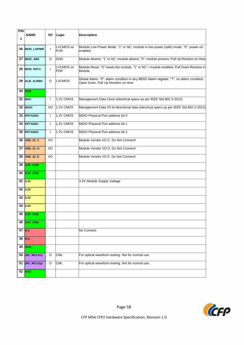
CFP MSA CFP2 Hardware Specification, Revision 1.0
PIN
#
NAME I/O Logic Description
26 MOD_LOPWR I LVCMOS w/ PUR
Module Low Power Mode. "1" or NC: module in low power (safe) mode, "0": power-on enabled
27 MOD_ABS O GND Module Absent. "1" or NC: module absent, "0": module present, Pull Up Resistor on Host
28 MOD_RSTn I LVCMOS w/ PDR
Module Reset. "0" resets the module, "1" or NC = module enabled, Pull Down Resistor in Module
29 GLB_ALRMn O LVCMOS Global Alarm. “0": alarm condition in any MDIO Alarm register, "1": no alarm condition, Open Drain, Pull Up Resistor on Host
30 GND
31 MDC I 1.2V CMOS Management Data Clock (electrical specs as per IEEE Std 802.3-2012)
32 MDIO I/O 1.2V CMOS Management Data I/O bi-directional data (electrical specs as per IEEE Std 802.3-2012)
33 PRTADR0 I 1.2V CMOS MDIO Physical Port address bit 0
34 PRTADR1 I 1.2V CMOS MDIO Physical Port address bit 1
35 PRTADR2 I 1.2V CMOS MDIO Physical Port address bit 2
36 VND_IO_C I/O Module Vendor I/O C. Do Not Connect!
37 VND_IO_D I/O Module Vendor I/O D. Do Not Connect!
38 VND_IO_E I/O Module Vendor I/O E. Do Not Connect!
39 3.3V_GND
40 3.3V_GND
41 3.3V 3.3V Module Supply Voltage
42 3.3V
43 3.3V
44 3.3V
45 3.3V_GND
46 3.3V_GND
47 N.C No Connect
48 N.C.
49 GND
50 (RX_MCLKn) O CML For optical waveform testing. Not for normal use.
51 (RX_MCLKp) O CML For optical waveform testing. Not for normal use.
52 GND
Page 59
CFP MSA CFP2 Hardware Specification, Revision 1.0
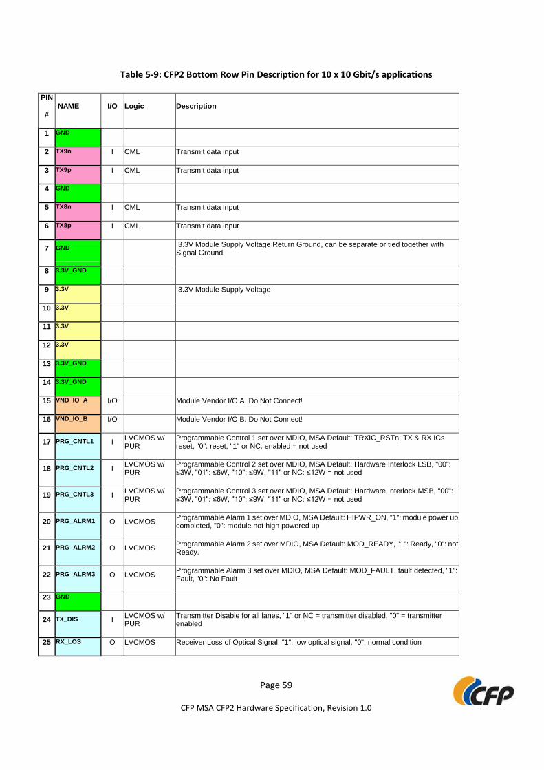
Table 5-9: CFP2 Bottom Row Pin Description for 10 x 10 Gbit/s applications
PIN
#
NAME I/O Logic Description
1 GND
2 TX9n I CML Transmit data input
3 TX9p I CML Transmit data input
4 GND
5 TX8n I CML Transmit data input
6 TX8p I CML Transmit data input
7 GND 3.3V Module Supply Voltage Return Ground, can be separate or tied together with Signal Ground
8 3.3V_GND
9 3.3V 3.3V Module Supply Voltage
10 3.3V
11 3.3V
12 3.3V
13 3.3V_GND
14 3.3V_GND
15 VND_IO_A I/O Module Vendor I/O A. Do Not Connect!
16 VND_IO_B I/O Module Vendor I/O B. Do Not Connect!
17 PRG_CNTL1 I LVCMOS w/ PUR
Programmable Control 1 set over MDIO, MSA Default: TRXIC_RSTn, TX & RX ICs reset, "0": reset, "1" or NC: enabled = not used
18 PRG_CNTL2 I LVCMOS w/ PUR
Programmable Control 2 set over MDIO, MSA Default: Hardware Interlock LSB, "00": ≤3W, "01": ≤6W, "10": ≤9W, "11" or NC: ≤12W = not used
19 PRG_CNTL3 I LVCMOS w/ PUR
Programmable Control 3 set over MDIO, MSA Default: Hardware Interlock MSB, "00": ≤3W, "01": ≤6W, "10": ≤9W, "11" or NC: ≤12W = not used
20 PRG_ALRM1 O LVCMOS Programmable Alarm 1 set over MDIO, MSA Default: HIPWR_ON, "1": module power up completed, "0": module not high powered up
21 PRG_ALRM2 O LVCMOS Programmable Alarm 2 set over MDIO, MSA Default: MOD_READY, "1": Ready, "0": not Ready.
22 PRG_ALRM3 O LVCMOS Programmable Alarm 3 set over MDIO, MSA Default: MOD_FAULT, fault detected, "1": Fault, "0": No Fault
23 GND
24 TX_DIS I LVCMOS w/ PUR
Transmitter Disable for all lanes, "1" or NC = transmitter disabled, "0" = transmitter enabled
25 RX_LOS O LVCMOS Receiver Loss of Optical Signal, "1": low optical signal, "0": normal condition
Page 60
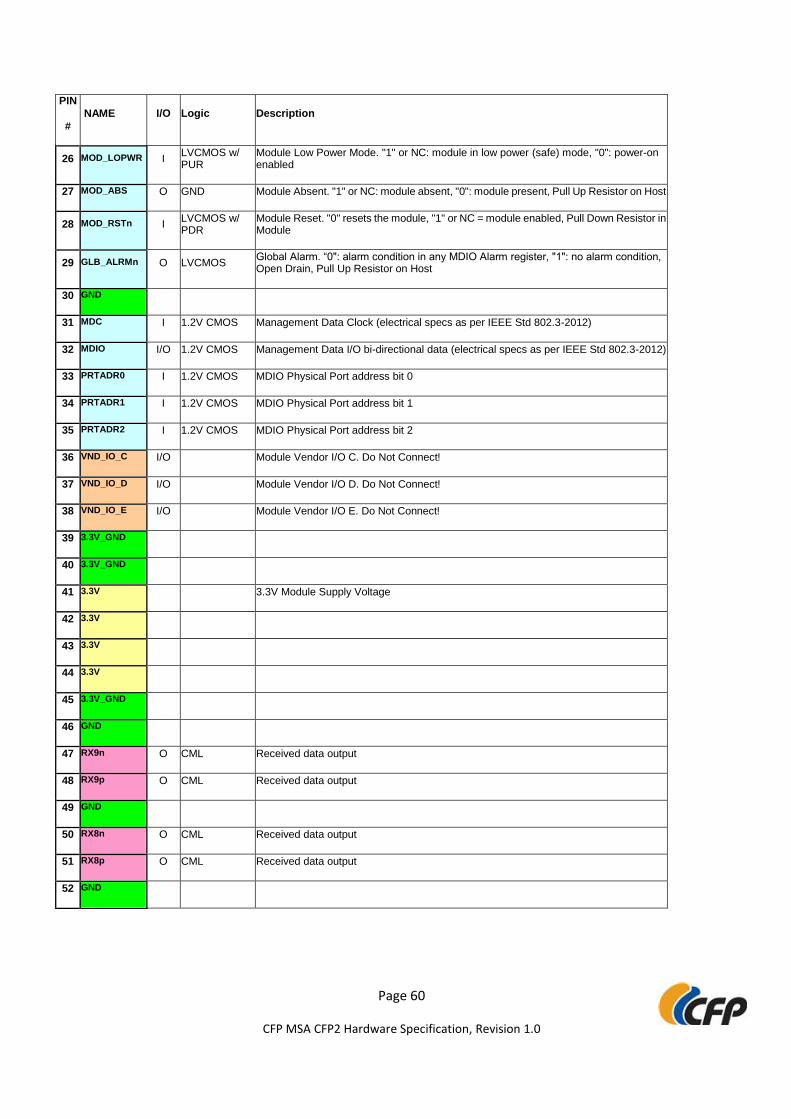
CFP MSA CFP2 Hardware Specification, Revision 1.0
PIN
#
NAME I/O Logic Description
26 MOD_LOPWR I LVCMOS w/ PUR
Module Low Power Mode. "1" or NC: module in low power (safe) mode, "0": power-on enabled
27 MOD_ABS O GND Module Absent. "1" or NC: module absent, "0": module present, Pull Up Resistor on Host
28 MOD_RSTn I LVCMOS w/ PDR
Module Reset. "0" resets the module, "1" or NC = module enabled, Pull Down Resistor in Module
29 GLB_ALRMn O LVCMOS Global Alarm. “0": alarm condition in any MDIO Alarm register, "1": no alarm condition, Open Drain, Pull Up Resistor on Host
30 GND
31 MDC I 1.2V CMOS Management Data Clock (electrical specs as per IEEE Std 802.3-2012)
32 MDIO I/O 1.2V CMOS Management Data I/O bi-directional data (electrical specs as per IEEE Std 802.3-2012)
33 PRTADR0 I 1.2V CMOS MDIO Physical Port address bit 0
34 PRTADR1 I 1.2V CMOS MDIO Physical Port address bit 1
35 PRTADR2 I 1.2V CMOS MDIO Physical Port address bit 2
36 VND_IO_C I/O Module Vendor I/O C. Do Not Connect!
37 VND_IO_D I/O Module Vendor I/O D. Do Not Connect!
38 VND_IO_E I/O Module Vendor I/O E. Do Not Connect!
39 3.3V_GND
40 3.3V_GND
41 3.3V 3.3V Module Supply Voltage
42 3.3V
43 3.3V
44 3.3V
45 3.3V_GND
46 GND
47 RX9n O CML Received data output
48 RX9p O CML Received data output
49 GND
50 RX8n O CML Received data output
51 RX8p O CML Received data output
52 GND

Page 61
CFP MSA CFP2 Hardware Specification, Revision 1.0
Table 5-10: CFP2 Bottom Row Pin Description for Multi-Port applications
PIN
#
NAME I/O Logic Description
1 GND
2 S3_TXn I CML Transmit data input
3 S3_TXp I CML Transmit data input
4 GND
5 S2_TXn I CML Transmit data input
6 S2_TXp I CML Transmit data input
7 GND 3.3V Module Supply Voltage Return Ground, can be separate or tied together with Signal Ground
8 3.3V_GND
9 3.3V 3.3V Module Supply Voltage
10 3.3V
11 3.3V
12 3.3V
13 3.3V_GND
14 3.3V_GND
15 VND_IO_A I/O Module Vendor I/O A. Do Not Connect!
16 VND_IO_B I/O Module Vendor I/O B. Do Not Connect!
17 PRG_CNTL1 I LVCMOS w/ PUR
Programmable Control 1 set over MDIO, MSA Default: TRXIC_RSTn, TX & RX ICs reset, "0": reset, "1" or NC: enabled = not used
18 PRG_CNTL2 I LVCMOS w/ PUR
Programmable Control 2 set over MDIO, MSA Default: Hardware Interlock LSB, "00": ≤3W, "01": ≤6W, "10": ≤9W, "11" or NC: ≤12W = not used
19 PRG_CNTL3 I LVCMOS w/ PUR
Programmable Control 3 set over MDIO, MSA Default: Hardware Interlock MSB, "00": ≤3W, "01": ≤6W, "10": ≤9W, "11" or NC: ≤12W = not used
20 PRG_ALRM1 O LVCMOS Programmable Alarm 1 set over MDIO, MSA Default: HIPWR_ON, "1": module power up completed, "0": module not high powered up
21 PRG_ALRM2 O LVCMOS Programmable Alarm 2 set over MDIO, MSA Default: MOD_READY, "1": Ready, "0": not Ready.
22 PRG_ALRM3 O LVCMOS Programmable Alarm 3 set over MDIO, MSA Default: MOD_FAULT, fault detected, "1": Fault, "0": No Fault
23 GND
24 TX_DIS I LVCMOS w/ PUR
Transmitter Disable for all lanes, "1" or NC = transmitter disabled, "0" = transmitter enabled
25 RX_LOS O LVCMOS Receiver Loss of Optical Signal, "1": low optical signal, "0": normal condition

Page 62
CFP MSA CFP2 Hardware Specification, Revision 1.0
PIN
#
NAME I/O Logic Description
26 MOD_LOPWR I LVCMOS w/ PUR
Module Low Power Mode. "1" or NC: module in low power (safe) mode, "0": power-on enabled
27 MOD_ABS O GND Module Absent. "1" or NC: module absent, "0": module present, Pull Up Resistor on Host
28 MOD_RSTn I LVCMOS w/ PDR
Module Reset. "0" resets the module, "1" or NC = module enabled, Pull Down Resistor in Module
29 GLB_ALRMn O LVCMOS Global Alarm. “0": alarm condition in any MDIO Alarm register, "1": no alarm condition, Open Drain, Pull Up Resistor on Host
30 GND
31 MDC I 1.2V CMOS Management Data Clock (electrical specs as per IEEE Std 802.3-2012)
32 MDIO I/O 1.2V CMOS Management Data I/O bi-directional data (electrical specs as per IEEE Std 802.3-2012)
33 PRTADR0 I 1.2V CMOS MDIO Physical Port address bit 0
34 PRTADR1 I 1.2V CMOS MDIO Physical Port address bit 1
35 PRTADR2 I 1.2V CMOS MDIO Physical Port address bit 2
36 VND_IO_C I/O Module Vendor I/O C. Do Not Connect!
37 VND_IO_D I/O Module Vendor I/O D. Do Not Connect!
38 VND_IO_E I/O Module Vendor I/O E. Do Not Connect!
39 3.3V_GND
40 3.3V_GND
41 3.3V 3.3V Module Supply Voltage
42 3.3V
43 3.3V
44 3.3V
45 3.3V_GND
46 GND
47 S3_RXn O CML Received data output
48 S3_RXp O CML Received data output
49 GND
50 S2_RXn O CML Received data output
51 S2_RXp O CML Received data output
52 GND
Page 63
CFP MSA CFP2 Hardware Specification, Revision 1.0
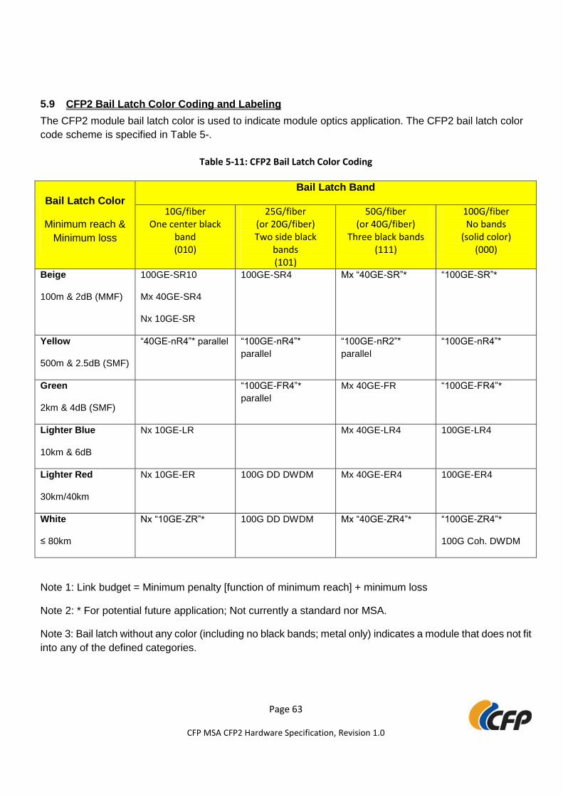
5.9 CFP2 Bail Latch Color Coding and Labeling
The CFP2 module bail latch color is used to indicate module optics application. The CFP2 bail latch color
code scheme is specified in Table 5-.
Table 5-11: CFP2 Bail Latch Color Coding
Bail Latch Color
Minimum reach &
Minimum loss
Bail Latch Band
10G/fiber One center black
band (010)
25G/fiber (or 20G/fiber) Two side black
bands (101)
50G/fiber (or 40G/fiber)
Three black bands (111)
100G/fiber No bands
(solid color) (000)
Beige
100m & 2dB (MMF)
100GE-SR10
Mx 40GE-SR4
Nx 10GE-SR
100GE-SR4
Mx “40GE-SR”*
“100GE-SR”*
Yellow
500m & 2.5dB (SMF)
“40GE-nR4”* parallel “100GE-nR4”*
parallel
“100GE-nR2”*
parallel
“100GE-nR4”*
Green
2km & 4dB (SMF)
“100GE-FR4”*
parallel
Mx 40GE-FR “100GE-FR4”*
Lighter Blue
10km & 6dB
Nx 10GE-LR Mx 40GE-LR4 100GE-LR4
Lighter Red
30km/40km
Nx 10GE-ER 100G DD DWDM Mx 40GE-ER4
100GE-ER4
White
≤ 80km
Nx “10GE-ZR”* 100G DD DWDM Mx “40GE-ZR4”* “100GE-ZR4”*
100G Coh. DWDM
Note 1: Link budget = Minimum penalty [function of minimum reach] + minimum loss
Note 2: * For potential future application; Not currently a standard nor MSA.
Note 3: Bail latch without any color (including no black bands; metal only) indicates a module that does not fit
into any of the defined categories.

Page 64
CFP MSA CFP2 Hardware Specification, Revision 1.0
The CFP2 module should be clearly labeled. The complete labeling need not be visible when the CFP2
module is installed in the host cage assembly. A recessed area on the bottom of the CFP2 module, as
shown in Figure 5-12, is the recommended location for module label.
Figure 5-12: CFP2 Module Label Recess
6 REGULATORY COMPLIANCE
Per Reference [1].
End of Document