CFM25S Series App Notes V16 - cincon.com
12
CFM25S Series Application Note V16 June 2020 1 Approved By: Department Approved By Checked By Written By Research and Development Department Enoch Wei-Cheng/Jason Joyce Ovid Quality Assurance Department Ryan Benny AC-DC Switching Power Module CFM25S Series APPLICATION NOTE
Transcript of CFM25S Series App Notes V16 - cincon.com

CFM25S Series
Application Note V16 June 2020
1
Approved By:
Department Approved By Checked By Written By
Research and Development Department
Enoch Wei-Cheng/Jason Joyce
Ovid
Quality Assurance Department
Ryan Benny
AC-DC Switching Power Module CFM25S Series
APPLICATION NOTE

CFM25S Series
Application Note V16 June 2020
2
Content 1. INTRODUCTION 3
2. CFM25S SERIES FEATURES 3
3. ELECTRICAL BLOCK DIAGRAM 3
4. TECHNICAL SPECIFICATIONS 4
5. MAIN FEATURES AND FUNCTIONS 7 5.1 Operating Temperature Range 7
5.2 Output Protection 7
5.3 Peak Load Function 7
6. EMC & SAFETY 7
7. APPLICATIONS 7 7.1 Power De-Rating Curve 7
7.2 Test Set-Up 8
7.3 Output Ripple and Noise Measurement 8
7.4 Installation Instruction 8
7.5 Class I EMI Solution 9
8. CFM25S SERIES MECHANICAL OUTLINE DIAGRAMS 10 8.1. Mechanical Outline Diagrams 10
8.2. Packing Information 10
9. PART NUMBER 12

CFM25S Series
Application Note V16 June 2020
3
1. Introduction This application note describes the features and functions of Cincon’s CFM25S series of open frame, switching AC-DC power module. These are highly efficient, reliable, compact, high power density, single output AC/DC power modules. The module is fully protected against short circuit and over-voltage conditions. Cincon’s world class automated manufacturing methods, together with an extensive testing and qualification program, ensure that the
CFM25S series power module is extremely reliable.
2. CFM25S Series Features • 25W Isolated Output
• Universal Input 90~264VAC
• High Efficiency Up to 87%
• Meets EN55032 Class B and CISRP/FCC Class B
• Meets IEC/EN60335-1, IEC61558-1
• Approved IEC/EN/UL62368
• Continuous Short Circuit Protection
• Over Voltage Protection
• Peak Load (2 Times of Rated Current)
• No Load Input Power < 0.1W
• Class II
3. Electrical Block Diagram

CFM25S Series
Application Note V16 June 2020
4
4. Technical Specifications
(All specifications are typical at nominal input, full load at 25 unless otherwise noted.)
ABSOLUTE MAXIMUM RATINGS
PARAMETER NOTES and CONDITIONS Device Min. Typical Max. Units
Input Voltage All 90 264 Vac
120 370 Vdc
Operating Temperature See derating curve All -30 70 0C
Storage Temperature All -30 85 0C
Input/Output Isolation Voltage 1 minute All 3000 Vac
Operating Altitude All 5000 m
INPUT CHARACTERISTICS
PARAMETER NOTES and CONDITIONS Device Min. Typical Max. Units
Operating Voltage Range All 100 240 Vac
Input Frequency Range All 47 63 Hz
Maximum Input Current 100% Load, Vin=100Vac All 0.7 A
Leakage Current All 0.25 mA
Inrush Current Vin=240Vac, cold start at 25. All 60 A
OUTPUT CHARACTERISTICS
PARAMETER NOTES and CONDITIONS Device Min. Typical Max. Units
Output Voltage Set Point Vin=Nominal Vin, Io=Io.max, Tc=25.
CFM25S050 4.9 5 5.1
Vdc
CFM25S120 11.88 12 12.12
CFM25S150 14.85 15 15.15
CFM25S240 23.76 24 24.24
CFM25S360 35.64 36 36.36
CFM25S480 47.52 48 48.48
Operating Output Current Range
CFM25S050 4
A
CFM25S120 2.1
CFM25S150 1.67
CFM25S240 1.05
CFM25S360 0.7
CFM25S480 0.52
Holdup Time Vin=115Vac All 8 ms
Output Voltage Regulation
Load Regulation 10% load to full load All ±1.0 %
Line Regulation Vin=high line to low line All ±1.0 %

CFM25S Series
Application Note V16 June 2020
5
PARAMETER NOTES and CONDITIONS Device Min. Typical Max. Units
Over Voltage Protection uses a TVS component to clamp output voltage
CFM25S050 6.45 6.8 7.44
VDC
CFM25S120 14.3 15 16.2
CFM25S150 17.1 18 18.9
CFM25S240 28.5 30 31.5
CFM25S360 40.9 43 45.6
CFM25S480 53.2 56 59.2
Output Ripple and Noise
1. Add a 0.1uF ceramic capacitor and a 10uF aluminum electrolytic capacitor to output.
2. Oscilloscope is 20MHz band width.
3. Ambient temperature=25
CFM25S050 50
mVp-p
CFM25S120 120
CFM25S150 150
CFM25S240 240
CFM25S360 360
CFM25S480 480
Load Capacitance
1. Ambient temperature=25
2. Input voltage is 115VAC and 230VAC
3. Output is max. load
CFM25S050 81000
uF
CFM25S120 40900
CFM25S150 19800
CFM25S240 6600
CFM25S360 4000
CFM25S480 2170
Efficiency
Output is rated load
Ambient temperature=25
@ Input voltage is 230VAC
CFM25S050 81
%
CFM25S120 84
CFM25S150 85
CFM25S240 86
CFM25S360 87
CFM25S480 87
ISOLATION CHARACTERISTICS
PARAMETER NOTES and CONDITIONS Device Min. Typical Max. Units
Input to Output 1 minute All 3000 Vac
Isolation Resistance All 100 MΩ
FEATURE CHARACTERISTICS
PARAMETER NOTES and CONDITIONS Device Min. Typical Max. Units
Switching Frequency All 65 KHz

CFM25S Series
Application Note V16 June 2020
6
GENERAL SPECIFICATIONS
PARAMETER NOTES and CONDITIONS Device Min. Typical Max. Units
MTBF Io=100%; Ta=25 per
MIL-HDBK-217FAll 500 K hours
Humidity Nom-condensing All 93 % RH
Shock
Mests MIL-STD-810F Table 516.5,TABLE 516.5-1 10ms, each axis 3 times(+-X、Y、Z axis)
All 75 g
Vibration
Mests MIL-STD-810F Table 514.5C-VIII,15~2000Hz, X、Y、Z
axis,1 hr(each axis),. toal 3 hrs. All 4 g
Weight
CFM25SXXX 38
g CFM25SXXX-E 75
CFM25SXXX-T 40
Safety Class II,IEC/EN/UL60950-1, IEC/EN/UL62368-1
EMC Emission EN55032 Class B ,EN61000-3-2:2014,EN61000-3-3:2013, EN61000-6-3:2012, EN61000-6-4:2011, 47 CFR FCC Part 15 Subpart B, Oct.2014
Class B
Conducted Disturbance EN55032,EN61000-6-3:2012,Class B, 47 CFR FCC Part 15 Subpart B Class B
Radiated Disturbance EN55032,EN61000-6-3:2012,Class B, 47 CFR FCC Part 15 Subpart B Class B
Harmonic Current Emissions EN61000-3-2:2014
Voltage Fluctuations & Flicker EN61000-3-3:2013
EMC Immunity EN55024, EN61204-3:2000, EN61000-6-1:2007, EN61000-6-2:2005
Electrostatic Discharge (ESD) IEC 61000-4-2:2008, Air Discharge:±8KV, Contact Discharge:±4KV Criterion A
Radio-Frequency, Continuous Radiated Disturbance IEC 61000-4-3:2010 Criterion A
Electrical Fast Transient (EFT) IEC 61000-4-4:2012, ±0.5kv, ±1kv, ±2kv Criterion A
Surge IEC 61000-4-5:2014, L-N: ±0.5kv, ±1kv, Criterion A
Conducted Disturbances, Induced by RF Fields IEC 61000-4-6:2013 Criterion A
Power Frequency Magnetic Field
IEC 61000-4-8:2009 Criterion A
Voltage Dips IEC 61000-4-11:2004, Dip: 30% Reduction, Dip >95% Reduction Criterion A
Voltage Interruptions IEC 61000-4-11:2004, >95% Reduction Criterion B

CFM25S Series
Application Note V16 June 2020
7
5. Main Features and Functions
5.1 Operating Temperature Range
The highly efficient design of Cincon’s CFM25S series power modules has resulted in their ability to operate within ambient temperature environments from -300C to 700C. Due consideration must be given to the de-rating curves when ascertaining the maximum power that can be drawn from the module. The maximum power which can be drawn is influenced by a number of factors, such as: Input voltage range
Permissible Output load (per derating curve)
5.2 Output Protection
The power modules provide full continuous short-circuit protection. The unit will auto recover once the short circuit is removed. To provide protection in a fault condition, the unit is equipped with internal over-current protection. The unit will operate normally once the fault condition is removed.
5.3 Peak Load Function
CFM25SXXX PL and CFM25SXXX-E PL has a very powerful peak load function which can provide twice the rated power. However, the duration of the peak load should be less than 10 seconds, with a maximum 10% duty cycle and must externally add a 33uF/ 400V capacitor to BC+ & BC-, but this is not needed when input is @ 220Vac.
6. EMC & Safety Emission and Immunity
EN55032 Class B, EN61000-3-2:2014, EN61000-3-3:2013, EN61000-6-3:2012, EN61000-6-4:2011, 47 CFR FCC Part 15
Subpart B (Class B), Oct.2014, EN55024, EN61204-3:2000, EN61000-6-1:2007, EN61000-6-2:2005
Safety Class II, IEC/EN/UL60950-1, IEC/EN/UL62368-1
7. Applications
7.1 Power De-Rating Curve
CFM25S050, CFM25S050-T
CFM25S120, CFM25S150, CFM25S240, CFM25S360,
CFM25S480, CFM25S120-T, CFM25S150-T,
CFM25S240-T, CFM25S360-T , CFM25S480-T,
CFM25SXXX-E

CFM25S Series
Application Note V16 June 2020
8
7.2 Test Set-Up
The basic test set-up to measure parameters such as efficiency and load regulation is shown in Figure 1. When testing the Cincon’s CFM25S series under any transient conditions, please ensure that the transient response of the source is sufficient to power the equipment under test. We can calculate the
Efficiency
Load regulation and line regulation.
The value of efficiency is defined as:
Where:
Vo is output voltage
Io is output current
Pin is input power
The value of load regulation is defined as:
Where:
VFL is the output voltage at full load
VNL is the output voltage at 10% load
The value of line regulation is defined as:
. 100%HL LL
LL
V VLine regV
−
= ×
Where:
VHL is the output voltage of maximum input voltage at full load.
VLL is the output voltage of minimum input voltage at full load.
V
A
LoadAC
Supply
+Vo
-Vo
L
N
Pin
+ Figure 1. CFM25S Series Test Setup
7.3 Output Ripple and Noise Measurement
The test set-up for noise and ripple measurements is shown in Figure 2 Measured method:
Add a 0.1 uF ceramic capacitor and a 10 uF electrolytic capacitor to output at 20 MHz Band Width.
CINCON
AC-DC power supply
80 cm
- +
C1
. . C1=0.1uF
C2=10uF
Output
C2
Electronic load
Oscilloscope
Input
AC or DC Power source
Figure 2. Output Voltage Ripple and Noise Measurement Set-Up
7.4 Installation Instruction
The CFM25SXXX-T has four 3.5mm diameter mounting
holes. Please use the mounting holes as follows: Insert the spacer (6mm diameter max.) of 8mm height or more to mount the unit. The vibration specification applies when the unit is mounted on 8mm spacers. Please allow 4mm side clearance from the components and all side of the PCB. Allow 5mm clearance above the highest parts on the PCB. Be especially careful to allow 8mm between the solder side of the PCB and the mounting surface. If the clearances are not sufficient, the specifications for isolation and withstand will not be valid.
The CFM25SXXX and CFM25SXXX-E mounting holes
are 1.5mm. Please allow 4mm side clearance from the
components and all side of the PCB and CASE. Allow
5mm clearance above the highest parts on the PCB and
CASE.

CFM25S Series
Application Note V16 June 2020
9
7.5 Class I EMI Solution
The CFM25S series need additional inductance and YCap to meet EN55032 CLASS B when test condition is Class I.If customers use in Class II systems, please ignore this section.
CFM25SXXX
CFM25SXXX-E
CFM25SXXX-T
Additional Inductance related parameters:
Specification Inductance Duplex Winding /turns Manufacturers
UU9.8 R12K 10mH 2-UEW φ0.27*85Ts SEND POWER
Additional Safety YCap related parameters:
Subclass WITHSTANDVOLTAGE Capacitance Manufacturers
Y1 CAP 250V(min) 1000pF(typ.) TDK

CFM25S Series
Application Note V16 June 2020
10
8. CFM25S Series Mechanical Outline Diagrams 8.1. Mechanical Outline Diagrams
Figure 3. CFM25S series Mechanical Outline Diagram
8.2. Packing Information The packing information for CFM25S SERIES is showing as follows:
2
2
3
1
CFM25S Product
Inner Box
3
2
1
PCSOUTSIDE DIM(mm)NAMEPART NO.
Partition
4
5
6
Antistatic Foam
No.148 Cardboard Box
G64304163
ITEM
Antistatic Foam
76x66x35mm
393x385x220mm
326x200x6mm
326x200x25mm
50.8x27.94x20.5mm 200
G64114346
G64301113
G643011147
373x200x25mm
20075x65x10mmAntistatic FoamG64308311
8
10065x10x10mmAntistatic FoamG64301178
Each Box Packaging 200 PCS ProductsNet weight Ref. 8 KgGross weight Ref. 9.5 Kg
78
G64U10075
5
6
100
1
1
3
4
2
CFM25S 200Pcs a box, including the total weight of package material about 9.5Kg

CFM25S Series
Application Note V16 June 2020
11
The packing information for CFM25S-E SERIES is showing as follows:
2
2
3
1
160G64308311
CFM25S-E Product
Antistatic Foam
Inner Box
4
3
2
1
PCSOUTSIDE DIM(mm)NAMEPART NO.
Partition5
6
7 Antistatic Foam
No.148 Cardboard Box
G64304175
ITEM
Antistatic Foam
75x65x10mm
76x66x45mm
393x385x220mm
326x200x6mm
326x200x25mm
53.1x30.3x24.8mm 160
G64114346
G64301113
G64301114
Each Box Packaging 160 PCS Products
Gross weight Ref. 14 KgNet weight Ref. 12.8 Kg
373x200x25mm
67
G64U10075
1
3
2
4
5
80
CFM25S-E 160Pcs a box, including the total weight of package material about 14Kg
The packing information for CFM25S-T SERIES is showing as follows:
326x200x25mm
288x200x25mm
326x200x6mm
388x300x220mm
70.5x27.94x20.5mm
115x65x35mm
115x65x5.5mm
Antistatic Foam
ITEM
G64304165
No.149 Cardboard Box
Antistatic Foam
7
6
5
Partition
PART NO. NAME OUTSIDE DIM PCS
1
2
3
4
Inner Box
Antistatic Foam
CFM25S-T Product
G64308313 50
100
50
1
1
2
2
G64114347
G64U10075
G64301115
G64301114
8
115x65x10mm 50G64308312 Antistatic Foam
50115x5x22mmAntistatic Foam
9
G64301182
Each Box Packaging 100 PCS ProductsNet weight Ref. 4.1 KgGross weight Ref. 5.3 Kg
8
9
1
5
2
4
36
7
CFM25S-T 100Pcs a box, including the total weight of package material about 5.3Kg
CFM25S Series
Application Note V16 June 2020
12
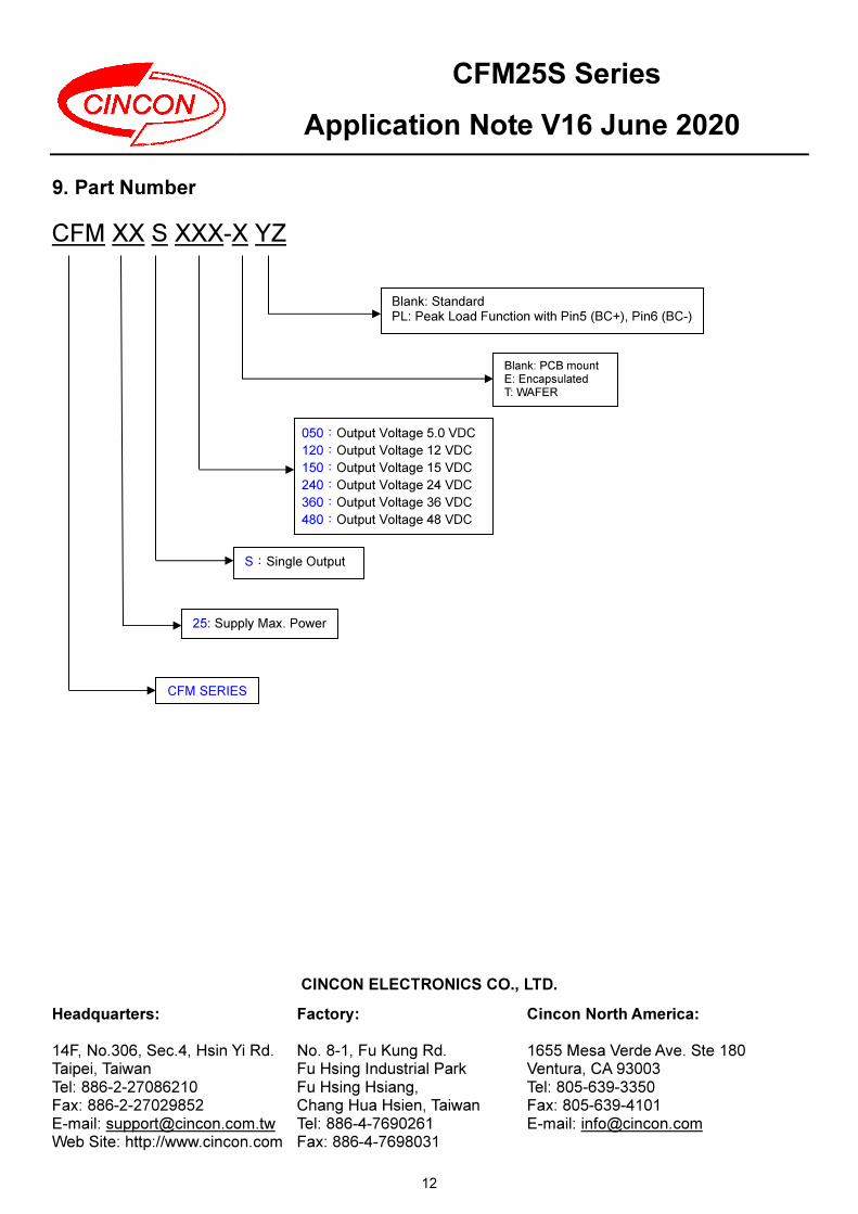
9. Part Number
CFM XX S XXX-X YZ
CINCON ELECTRONICS CO., LTD.
Headquarters: 14F, No.306, Sec.4, Hsin Yi Rd. Taipei, Taiwan Tel: 886-2-27086210 Fax: 886-2-27029852 E-mail: [email protected] Web Site: http://www.cincon.com
Factory: No. 8-1, Fu Kung Rd. Fu Hsing Industrial Park Fu Hsing Hsiang, Chang Hua Hsien, Taiwan Tel: 886-4-7690261 Fax: 886-4-7698031
Cincon North America: 1655 Mesa Verde Ave. Ste 180 Ventura, CA 93003 Tel: 805-639-3350 Fax: 805-639-4101 E-mail: [email protected]
CFM SERIES
25: Supply Max. Power
S:Single Output
050:Output Voltage 5.0 VDC
120:Output Voltage 12 VDC
150:Output Voltage 15 VDC
240:Output Voltage 24 VDC
360:Output Voltage 36 VDC
480:Output Voltage 48 VDC
Blank: PCB mount E: Encapsulated T: WAFER
Blank: Standard PL: Peak Load Function with Pin5 (BC+), Pin6 (BC-)