CELL PROPERTIES AND DESIGN - University of Cincinnati · CELL PROPERTIES AND DESIGN 4.1...
17
CELL PROPERTIES AND DESIGN 4.1 EFFICIENCIES Under laboratory conditions, with current state-of-the-art technology, it is possible to produce single-crystal silicon solar cells with efficiencies in excess of 24%. However, commercially mass-produced cells are typically only 13–14% efficient. There are many reasons for this; the over-riding one being that, while efficiency can be the major aim for laboratory produced cells, irrespective of cost, complexity of processing or throughput, in general, laboratory techniques are unsuited to industry. Solar cell research continues to improve the efficiency of cells towards the currently accepted theoretical limit of about 30%. Commercial products lag some years behind laboratory results, but commercial module efficiencies of over 20% could be see in coming years. Higher efficiency makes a dramatic difference to the cost of photovoltaics as an electricity source, since fewer modules are required for a given power output. The cost of electricity generated by a photovoltaic system therefore depends on its initial cost, operating life, operating costs and electricity output, as well as the costs of borrowing money and the rate at which current monetary values are discounted over time. These factors can be represented by a standard economic discounted cash flow equation: Chapter 4
Transcript of CELL PROPERTIES AND DESIGN - University of Cincinnati · CELL PROPERTIES AND DESIGN 4.1...
CELL PROPERTIES AND DESIGN
4.1 EFFICIENCIES
Under laboratory conditions, with current state-of-the-art technology, it is possible to produce single-crystal silicon solar cells with efficiencies in excess of 24%. However, commercially mass-produced cells are typically only 13–14% efficient. There are many reasons for this; the over-riding one being that, while efficiency can be the major aim for laboratory produced cells, irrespective of cost, complexity of processing or throughput, in general, laboratory techniques are unsuited to industry.
Solar cell research continues to improve the efficiency of cells towards the currently accepted theoretical limit of about 30%. Commercial products lag some years behind laboratory results, but commercial module efficiencies of over 20% could be see in coming years. Higher efficiency makes a dramatic difference to the cost of photovoltaics as an electricity source, since fewer modules are required for a given power output. The cost of electricity generated by a photovoltaic system therefore depends on its initial cost, operating life, operating costs and electricity output, as well as the costs of borrowing money and the rate at which current monetary values are discounted over time. These factors can be represented by a standard economic discounted cash flow equation:
Chapter
4
58
t
tt
t
tttt
rE
rFUELMOACC
C1
1&
(4.1)
where ACCt is the capital cost in year t, O&Mt is total operating and maintenance cost in year t, FUELt is the fuel cost in year t (if applicable, e.g. for a RAPS system), Et is the energy produced in year t, and r is the discount rate.
Both increased efficiencies and reduced wafer costs are critical to overall photovoltaic price reductions since, with current single crystal or polycrystalline silicon technology, wafer costs account for about half of the finished module cost per watt, even at production levels of 10 MW per annum (Darkazalli et al., 1991). Factors affecting cell efficiency are discussed below.
4.2 OPTICAL LOSSES
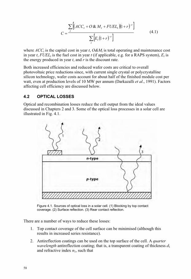
Optical and recombination losses reduce the cell output from the ideal values discussed in Chapters 2 and 3. Some of the optical loss processes in a solar cell are illustrated in Fig. 4.1.
Figure 4.1. Sources of optical loss in a solar cell. (1) Blocking by top contact coverage. (2) Surface reflection. (3) Rear contact reflection.
There are a number of ways to reduce these losses:
1. Top contact coverage of the cell surface can be minimised (although this results in increased series resistance).
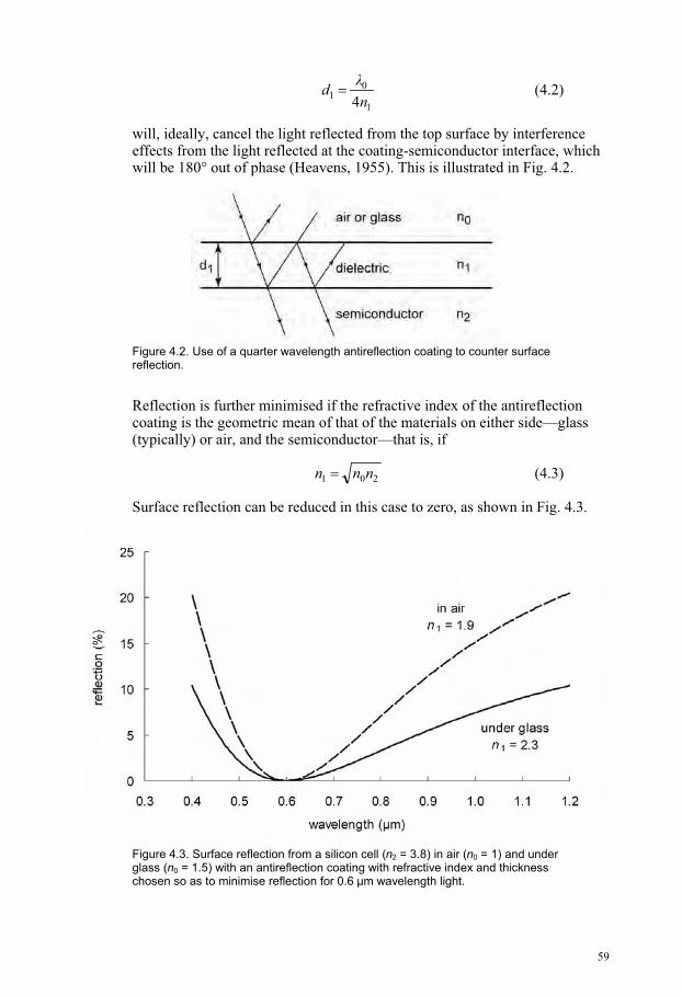
2. Antireflection coatings can be used on the top surface of the cell. A quarterwavelength antireflection coating; that is, a transparent coating of thickness d1
and refractive index n1, such that
59
1
01
4nd (4.2)
will, ideally, cancel the light reflected from the top surface by interference effects from the light reflected at the coating-semiconductor interface, which will be 180° out of phase (Heavens, 1955). This is illustrated in Fig. 4.2.
Figure 4.2. Use of a quarter wavelength antireflection coating to counter surface reflection.
Reflection is further minimised if the refractive index of the antireflection coating is the geometric mean of that of the materials on either side—glass (typically) or air, and the semiconductor—that is, if
201 nnn (4.3)
Surface reflection can be reduced in this case to zero, as shown in Fig. 4.3.
Figure 4.3. Surface reflection from a silicon cell (n2 = 3.8) in air (n0 = 1) and under glass (n0 = 1.5) with an antireflection coating with refractive index and thickness chosen so as to minimise reflection for 0.6 m wavelength light.
60
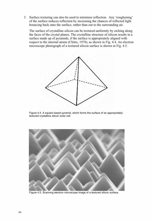
3. Surface texturing can also be used to minimise reflection. Any ‘roughening’ of the surface reduces reflection by increasing the chances of reflected light bouncing back onto the surface, rather than out to the surrounding air.
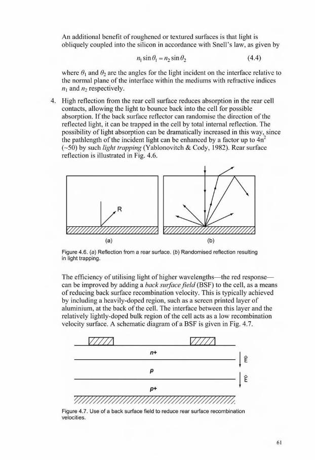
The surface of crystalline silicon can be textured uniformly by etching along the faces of the crystal planes. The crystalline structure of silicon results in a surface made up of pyramids, if the surface is appropriately aligned with respect to the internal atoms (Chitre, 1978), as shown in Fig. 4.4. An electron microscope photograph of a textured silicon surface is shown in Fig. 4.5.
Figure 4.4. A square based pyramid, which forms the surface of an appropriately-textured crystalline silicon solar cell.
Figure 4.5. Scanning electron microscope image of a textured silicon surface.
62
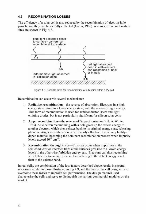
4.3 RECOMBINATION LOSSES
The efficiency of a solar cell is also reduced by the recombination of electron-hole pairs before they can be usefully collected (Green, 1986). A number of recombination sites are shown in Fig. 4.8.
Figure 4.8. Possible sites for recombination of e-h pairs within a PV cell.
Recombination can occur via several mechanisms:
1. Radiative recombination—the reverse of absorption. Electrons in a high energy state return to a lower energy state, with the release of light energy. This form of recombination is used for semiconductor lasers and light emitting diodes, but is not particularly significant for silicon solar cells.
2. Auger recombination—the reverse of ‘impact ionisation’ (Hu & White, 1983). An electron recombining with a hole gives up the excess energy to another electron, which then relaxes back to its original energy state, releasing phonons. Auger recombination is particularly effective in relatively highly-doped material, becoming the dominant recombination process when impurity levels exceed 1017 cm–3.
3. Recombination through traps—This can occur when impurities in the semiconductor or interface traps at the surfaces give rise to allowed energy levels in the otherwise forbidden energy gap. Electrons can thus recombine with holes in a two-stage process, first relaxing to the defect energy level, then to the valence band.
In real cells, the combination of the loss factors described above results in spectral responses similar to those illustrated in Fig 4.9, and the task of the cell designer is to overcome these losses to improve cell performance. The design features used characterise the cells and serve to distinguish the various commercial modules on the market.
63
Figure 4.9. Typical external quantum efficiency and responsivity in actual solar cells, illustrating the impact of optical and recombination losses.
4.4 TOP CONTACT DESIGN
Metallic top contacts are necessary to collect the current generated by a solar cell. Busbars are connected directly to the external leads, while fingers are finer areas of metallisation that collect current for delivery to the busbars. A simple top contact design is shown in Fig. 4.10. Top contact design aims to optimise current collection against losses owing to internal resistances and cell shadowing.
finger
busbar
Figure 4.10. Top contact design of a solar cell.
4.4.1 Bulk and sheet resistivities
Generated current typically flows perpendicular to the cell surface from the bulk of the cell and then laterally through the top doped layer until it is collected at a top surface contact, as shown in Fig. 4.11.
The resistance to the current of the bulk component of the cell, or the bulk resistance (Rb) is defined as
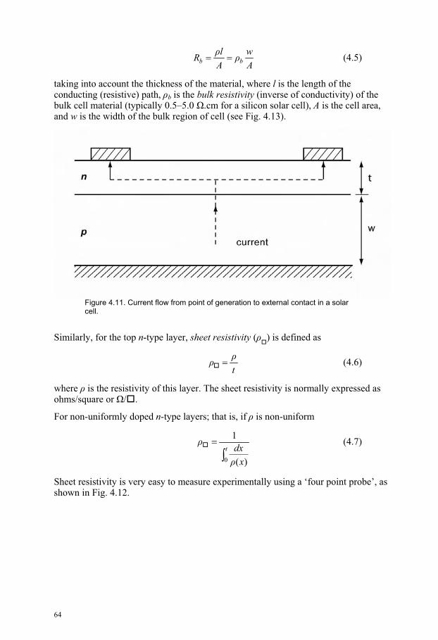
64
A
w
A
lR bb (4.5)
taking into account the thickness of the material, where l is the length of the conducting (resistive) path, b is the bulk resistivity (inverse of conductivity) of the bulk cell material (typically 0.5–5.0 .cm for a silicon solar cell), A is the cell area, and w is the width of the bulk region of cell (see Fig. 4.13).
Figure 4.11. Current flow from point of generation to external contact in a solar cell.
Similarly, for the top n-type layer, sheet resistivity ( ) is defined as
t (4.6)
where is the resistivity of this layer. The sheet resistivity is normally expressed as ohms/square or / .
For non-uniformly doped n-type layers; that is, if is non-uniform
t
x
dx0 )(
1 (4.7)
Sheet resistivity is very easy to measure experimentally using a ‘four point probe’, as shown in Fig. 4.12.
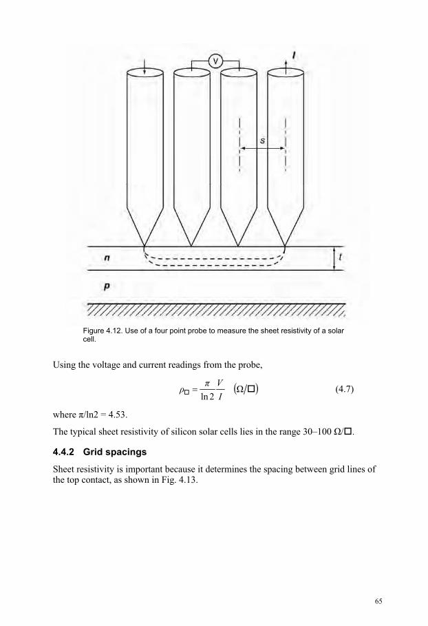
65
Figure 4.12. Use of a four point probe to measure the sheet resistivity of a solar cell.
Using the voltage and current readings from the probe,
2ln I
V (4.7)
where /ln2 = 4.53.
The typical sheet resistivity of silicon solar cells lies in the range 30–100 / .
4.4.2 Grid spacings
Sheet resistivity is important because it determines the spacing between grid lines of the top contact, as shown in Fig. 4.13.
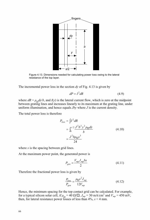
66
s/2
b
dy
y
fingers
Figure 4.13. Dimensions needed for calculating power loss owing to the lateral resistance of the top layer.
The incremental power loss in the section dy of Fig. 4.13 is given by
dRIdP 2 (4.9)
where dR = dy/b, and I(y) is the lateral current flow, which is zero at the midpoint between grating lines and increases linearly to its maximum at the grating line, under uniform illumination, and hence equals Jby where J is the current density.
The total power loss is therefore
24
32
2/
0
222
2
sbJ
b
dyybJ
dRIP
s
loss
(4.10)
where s is the spacing between grid lines.
At the maximum power point, the generated power is
2
bsJVP mpmp
gen (4.11)
Therefore the fractional power loss is given by
mp
mp
gen
loss
V
Js
P
P
12
2
(4.12)
Hence, the minimum spacing for the top contact grid can be calculated. For example, for a typical silicon solar cell, if = 40 / , Jmp = 30 mA/cm2 and Vmp = 450 mV, then, for lateral resistance power losses of less than 4%, s < 4 mm.
67
4.4.3 Other losses
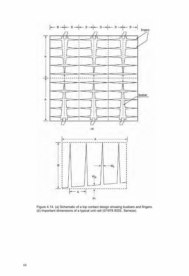
The busbars and fingers are the source of a variety of losses, in addition to the lateral current flow losses described previously. These include shading losses, resistive losses and contact resistance losses. A symmetrical contacting scheme, as shown in Fig. 4.14a, can be broken down into unit cells, as in Fig. 4.14b.
In brief, it can be shown (Serreze, 1978) that:
1. The optimum width of the busbar (Wb) occurs when the resistive loss in the busbar equals its shadowing loss.
2. A tapered busbar has lower losses than a busbar of constant width.
3. The smaller the unit cell, the finger width (Wf) and the finger spacings (s), the lower the losses.
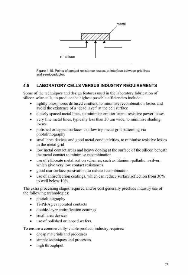
Obviously the third point must be countered by the need to allow light to enter the cell, as well as to allow practical manufacturing. Contact resistance losses at the interface between the grid lines and the semiconductor (see Fig. 4.15) are more important for fingers than busbars. To keep top contact losses low, the top n+ layer must be as heavily doped as possible. This ensures small sheet resistivities ( ) and hence low contact resistance losses.
However, a high doping level creates other problems. If a high level of phosphorus is diffused into silicon, the excess phosphorus lies at the surface of the cell, creating a ‘dead layer’, where light-generated carriers have little chance of being collected. Many commercial cells have a poor ‘blue’ response because of this dead layer.
68
Figure 4.14. (a) Schematic of a top contact design showing busbars and fingers. (b) Important dimensions of a typical unit cell (©1978 IEEE, Serreze).
69
metal
n+ silicon
Figure 4.15. Points of contact resistance losses, at interface between grid lines and semiconductor.
4.5 LABORATORY CELLS VERSUS INDUSTRY REQUIREMENTS
Some of the techniques and design features used in the laboratory fabrication of silicon solar cells, to produce the highest possible efficiencies include:
lightly phosphorus diffused emitters, to minimise recombination losses and avoid the existence of a ‘dead layer’ at the cell surface
closely spaced metal lines, to minimise emitter lateral resistive power losses
very fine metal lines, typically less than 20 m wide, to minimise shading losses
polished or lapped surfaces to allow top metal grid patterning via photolithography
small area devices and good metal conductivities, to minimise resistive losses in the metal grid
low metal contact areas and heavy doping at the surface of the silicon beneath the metal contact to minimise recombination
use of elaborate metallisation schemes, such as titanium-palladium-silver, which give very low contact resistances
good rear surface passivation, to reduce recombination
use of antireflection coatings, which can reduce surface reflection from 30% to well below 10%.
The extra processing stages required and/or cost generally preclude industry use of the following technologies:
photolithography
Ti-Pd-Ag evaporated contacts
double-layer antireflection coatings
small area devices
use of polished or lapped wafers.
To ensure a commercially-viable product, industry requires:
cheap materials and processes
simple techniques and processes
high throughput
70
large area devices
large contact areas
processes compatible with textured surfaces.
Typical commercially mass-produced solar cells use the following processing sequence:
1. Texturing of surfaces to form pyramids, which decrease the percentage of incident light reflected from the cell from about 33 to 11%, by causing reflected light from the pyramid face to strike at least one other pyramid face before escaping from the surface.
2. Phosphorus diffusion of the top surface, to provide a thin but heavily doped n-type layer.
3. Screen-printing and firing of aluminium or aluminium-doped silver paste onto the rear of the cell, to produce a back surface field and a rear metal contact.
4. Chemical cleaning.
5. Screen-printing and firing of front silver metal contact.
6. Edge junction isolation to destroy the conducting path between the front and rear metal contacts.
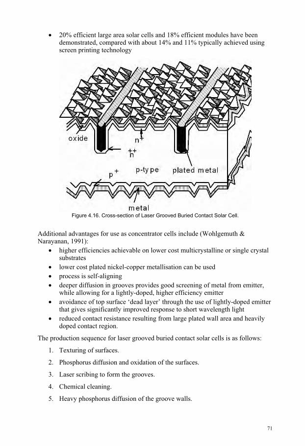
4.6 THE LASER GROOVED, BURIED CONTACT SOLAR CELL
A novel metallisation scheme, whereby laser grooves define the location and cross-sectional shape of the top surface metal conductors, has been developed at the University of New South Wales’ Centre for Photovoltaic Engineering. It is now in large scale commercial production by BP Solar in Spain, and marketed as the ‘Saturn’ cell. The new cell structure is called a ‘Laser Grooved, Buried Contact Solar Cell’ (BCSC), and is illustrated in cross section in Fig. 4.16.
The benefits of the BCSC over conventional cell manufacturing processes are:
large metal aspect ratios (contact thickness / width)
very fine top contact grid lines (20 m wide)
reduction of shading losses on large area devices from 10–15% in screen printed cells to 2–3%
excellent fill factors owing to low resistive losses in the metallisation and low contact resistance
increased metal cross-sections, without increasing shading, by increasing groove depth with the same width
device sizes can be increased without performance loss
no photolithography, antireflection coatings, polished or lapped surfaces or expensive materials such as Ti-Pd-Ag metallisation are required
very simple process
generate electricity at significantly lower cost than standard screen-printed sequence (Jordan & Nagle, 1994)
71
20% efficient large area solar cells and 18% efficient modules have been demonstrated, compared with about 14% and 11% typically achieved using screen printing technology
Figure 4.16. Cross-section of Laser Grooved Buried Contact Solar Cell.
Additional advantages for use as concentrator cells include (Wohlgemuth & Narayanan, 1991):
higher efficiencies achievable on lower cost multicrystalline or single crystal substrates
lower cost plated nickel-copper metallisation can be used
process is self-aligning
deeper diffusion in grooves provides good screening of metal from emitter, while allowing for a lightly-doped, higher efficiency emitter
avoidance of top surface ‘dead layer’ through the use of lightly-doped emitter that gives significantly improved response to short wavelength light
reduced contact resistance resulting from large plated wall area and heavily doped contact region.
The production sequence for laser grooved buried contact solar cells is as follows:
1. Texturing of surfaces.
2. Phosphorus diffusion and oxidation of the surfaces.
3. Laser scribing to form the grooves.
4. Chemical cleaning.
5. Heavy phosphorus diffusion of the groove walls.
72
6. Application and firing of aluminium onto the rear surface.
7. Electroless plating of front and rear contacts simultaneously (Ni-Cu-Ag).
8. Edge isolation.
An improved process for the BCSC was developed in 1993, which is capable of higher efficiencies at lower cost. The primary differences are the use of boron-diffused grooves at the rear and elimination of the aluminium deposition and firing steps (Honsberg et al., 1993).
E X E R C I S E S
4.1 (a) Give an overview of techniques currently used for silicon substrate formation.
(b) What are the advantages and disadvantages of each?
(c) Do crystalline silicon substrates have a long-term future?
4.2 (a) What substrate materials, other than silicon, can solar cells be made from?
(b) What are the advantages and disadvantages of each?
(c) Are some substrate materials better suited to specific applications or environments compared to others?
4.3 In block diagram form, outline the processing steps required to convert quartzite into a silicon space cell.
4.4 (a) Draw the cross-section of a typical commercial solar cell, marking relevant parts.
(b) Briefly describe how a solar cell operates.
(c) Outline important aspects of solar cell design that affect efficiency.
4.5 Commercially mass-produced solar cells for terrestrial applications have always had significantly lower generating efficiencies than the best laboratory fabricated cells. Discuss the reasons for and the effects of the differences in approaches and processing techniques between the two environments, and explain why these lead to such different levels of performance.
4.6 A certain technology produces 10% efficient solar modules at a cost of $1 per peak watt output under bright sunshine (1 kW/2). In a particular application, those balance-of-system costs that depend on the area of the array deployed amount to $80/m2. Assuming that other costs are identical in each case, at what price would 5% efficient modules produced by a second technology have to sell to give similar overall system costs?
4.7 (a) Derive an expression for the fractional power loss due to lateral current flow in the diffused top layer of a silicon solar cell.
73
(b) A commercial cell has a top layer sheet resistivity of 35 / and gives its maximum power output at a voltage of 420 mV and a current density of 28 mA/cm2. If the finger spacing is 3 mm, calculate the fractional power loss owing to lateral current flows in the diffused top layer.
(c) If the bulk substrate resistivity is 1 .cm and the substrate is 350 mthick, estimate the fractional power loss due to current flow in the substrate.
4.8 Calculate and sketch the upper limit to the spectral sensitivity (short circuit current/power in incident monochromatic light) as a function of wavelength for a silicon solar cell.
R E F E R E N C E S
Chitre, S.R. (1978), ‘A high volume cost efficient production macrostructuring process’, Proc. 14th IEEE Photovoltaic Specialists Conference, Washington, DC, pp. 152–154.
Darkazalli, G., Hogan, S. & Nowlan, M. (1991), ‘Sensitivity analysis and evaluation of manufacturing cost of crystalline silicon PV modules’, Proc. 22nd IEEE Photovoltaic Specialists Conference, Las Vegas, pp. 818–821.
Green, M.A. (1986), Solar Cells: Operating Principles, Technology and System Applications, University of NSW, Kensington, Australia.
Heavens, E.S. (1955), Optical Properties of Thin Solid Films, Butterworths, London.
Honsberg, C.B., Yun, F., Ebong, A., Taouk, M., Wenham, S.R. & Green, M.A. (1993), ‘685 mV open circuit voltage laser grooved silicon solar cell’, Technical Digest of the International PVSEC-7, Nagoya, Japan, pp. 89–90.
Hu, C. & White, R.M. (1983), Solar Cells: From Basic to Advanced Systems,McGraw-Hill, New York.
Jordan, D. & Nagel, J.P. (1994), ‘New generation of high efficiency solar cells: Development, processing and marketing’, Progress in Photovoltaics, 2, pp. 171–176.
Serreze, H.B. (1978), ‘Optimising solar cell performance by simultaneous consideration of grid pattern design and interconnect configurations’, Proc. 13th IEEE Photovoltaic Specialists Conference, Washington, DC, pp. 609–614.
Wohlgemuth, J.H. & Narayanan, S. (1991), ‘Buried contact concentrator solar cells’, Proc. 22nd IEEE Photovoltaic Specialists Conference, Las Vegas, pp. 273–277.
Yablonovitch, E. & Cody, G.D. (1982), ‘Intensity enhancement in textured optical sheets for solar cells’, IEEE Transactions on Electron Devices, ED-29, pp. 300–305.