Cell Assignment in Hybrid CMOS/Nanodevices Architecture ... · Cell Assignment in Hybrid...
12
653 Journal of Applied Research and Technology Cell Assignment in Hybrid CMOS/Nanodevices Architecture Using a PSO/SA Hybrid Algorithm Sadiq M. Sait* 1, 2 , Ahmad T. Sheikh 1 , Aiman H. El-Maleh 1 1 Department of Computer Engineering. 2 Center for Communications and IT Research, Research Institute. King Fahd University of Petroleum & Minerals. Dhahran-31261, Saudi Arabia. *[email protected] ABSTRACT In recent years, substantial advancements have been made in VLSI technology. With the introduction of CMOL (Cmos\nanowire\MOLecular Hybrid), higher circuit densities are possible. In CMOL there is an additional layer of nanofabric on top of CMOS stack. Nanodevices that lie between overlapping nanowires are programmable and can implement any combinational logic using a netlist of NOR gates. The limitation on the length of nanowires put a constraint on the connectivity domain of a circuit. The gates connected to each other must be within a connectivity radius; otherwise an extra buffer is inserted to connect them. Particle swarm optimization (PSO) has been used in a variety of problems that are NP- hard. PSO compared to the other iterative heuristic techniques is simpler to implement. Besides, it delivers comparable results. In this paper, a hybrid of PSO and simulated annealing (SA) for solving the cell assignment in CMOL, an NP-hard problem, is proposed. The proposed method takes advantage of the exploration and exploitation factors of PSO and the intrinsic hill climbing feature of SA to reduce the number of buffers to be inserted. Experiments conducted on ISCAS’89 benchmark circuits and a comparison with other heuristic techniques, are presented. Results showed that the proposed hybrid algorithm achieved better solution in terms of buffer count in reasonable time. Keywords: CMOL, combinatorial optimization, search heuristics, nanofabric, assignment, VLSI, hybrid heuristics. 1. Introduction In recent years, we have witnessed a tremendous development in the field of VLSI. We have seen the appearance of novel nanodevices, nanocircuits, nano-crossbar arrays [1], manufactured by nano- imprint lithography [2], CMOS/nano co-design architectures [3], and, their applications [5], [1]. Likharev and his colleagues [3], [4], developed the idea of CMOL (Cmos\nanowire\MOLecular Hybrid) for nanoelectronic devices. One of the problems in CMOL based circuit design is cell assignment. The CMOL cell assignment problem can be modeled as a special case of cell assignment problem on an FPGA, where one of the main objectives is to reduce the overall wire length. Whereas in CMOL, the goal is to place the connected cells close to each other with the constraint that these connected cells lie within a given radius from each other. Considerable amount of work has been done to tackle this problem. Strukov et al. proposed a deterministic algorithm [15], suitable for small circuits. Non-deterministic heuristic algorithms such as tabu search, particle swarm and simulated annealing have been widely used to solve a multitude of combinatorial optimization problems [20, 21, 22]. Xia Y. et al used genetic algorithm (GA) and laid the foundation to solve CMOL cell assignment problem using iterative heuristic algorithms [17]. The GA was able to find good solutions within acceptable time for circuits of varying complexity. Memetic algorithm (MA) an improvement of GA proposed by Z. Chu et al. [18], is a combination of GA and simulated annealing (SA). Another recent improvement proposed by Y. Xia et al. [19] combines Lagrangian relaxation (LR) technique and MA, hence the name LRMA, to solve the CMOL cell assignment problem. Higher quality solutions in terms of computational time and solution quality are reported with LRMA as compared to both GA and MA. Ideas on combining strengths of different heuristics have been around for some time. In the past SA has been used effectively as a hybrid with other algorithms like tabu search (TS), genetic algorithm (GA) and simulated evolution (SimE) [11]. The
-
Upload
hoangduong -
Category
Documents
-
view
219 -
download
0
Transcript of Cell Assignment in Hybrid CMOS/Nanodevices Architecture ... · Cell Assignment in Hybrid...
653Journal of Applied Research and Technology
Cell Assignment in Hybrid CMOS/Nanodevices Architecture Using a PSO/SA Hybrid Algorithm Sadiq M. Sait*1, 2, Ahmad T. Sheikh1, Aiman H. El-Maleh1
1 Department of Computer Engineering. 2 Center for Communications and IT Research, Research Institute. King Fahd University of Petroleum & Minerals. Dhahran-31261, Saudi Arabia. *[email protected] ABSTRACT In recent years, substantial advancements have been made in VLSI technology. With the introduction of CMOL (Cmos\nanowire\MOLecular Hybrid), higher circuit densities are possible. In CMOL there is an additional layer of nanofabric on top of CMOS stack. Nanodevices that lie between overlapping nanowires are programmable and can implement any combinational logic using a netlist of NOR gates. The limitation on the length of nanowires put a constraint on the connectivity domain of a circuit. The gates connected to each other must be within a connectivity radius; otherwise an extra buffer is inserted to connect them. Particle swarm optimization (PSO) has been used in a variety of problems that are NP-hard. PSO compared to the other iterative heuristic techniques is simpler to implement. Besides, it delivers comparable results. In this paper, a hybrid of PSO and simulated annealing (SA) for solving the cell assignment in CMOL, an NP-hard problem, is proposed. The proposed method takes advantage of the exploration and exploitation factors of PSO and the intrinsic hill climbing feature of SA to reduce the number of buffers to be inserted. Experiments conducted on ISCAS’89 benchmark circuits and a comparison with other heuristic techniques, are presented. Results showed that the proposed hybrid algorithm achieved better solution in terms of buffer count in reasonable time. Keywords: CMOL, combinatorial optimization, search heuristics, nanofabric, assignment, VLSI, hybrid heuristics.
1. Introduction In recent years, we have witnessed a tremendous development in the field of VLSI. We have seen the appearance of novel nanodevices, nanocircuits, nano-crossbar arrays [1], manufactured by nano-imprint lithography [2], CMOS/nano co-design architectures [3], and, their applications [5], [1]. Likharev and his colleagues [3], [4], developed the idea of CMOL (Cmos\nanowire\MOLecular Hybrid) for nanoelectronic devices. One of the problems in CMOL based circuit design is cell assignment. The CMOL cell assignment problem can be modeled as a special case of cell assignment problem on an FPGA, where one of the main objectives is to reduce the overall wire length. Whereas in CMOL, the goal is to place the connected cells close to each other with the constraint that these connected cells lie within a given radius from each other. Considerable amount of work has been done to tackle this problem. Strukov et al. proposed a deterministic algorithm [15], suitable for small circuits. Non-deterministic heuristic algorithms such as tabu search, particle swarm and
simulated annealing have been widely used to solve a multitude of combinatorial optimization problems [20, 21, 22]. Xia Y. et al used genetic algorithm (GA) and laid the foundation to solve CMOL cell assignment problem using iterative heuristic algorithms [17]. The GA was able to find good solutions within acceptable time for circuits of varying complexity. Memetic algorithm (MA) an improvement of GA proposed by Z. Chu et al. [18], is a combination of GA and simulated annealing (SA). Another recent improvement proposed by Y. Xia et al. [19] combines Lagrangian relaxation (LR) technique and MA, hence the name LRMA, to solve the CMOL cell assignment problem. Higher quality solutions in terms of computational time and solution quality are reported with LRMA as compared to both GA and MA. Ideas on combining strengths of different heuristics have been around for some time. In the past SA has been used effectively as a hybrid with other algorithms like tabu search (TS), genetic algorithm (GA) and simulated evolution (SimE) [11]. The

Cell Assignment in Hybrid CMOS/Nanodevices Architecture Using a PSO/SA Hybrid Algorithm, Sadiq M. Sait et al./653‐664
Vol. 11, October 2013 654
basic idea of hybridization is to enhance the strengths and compensate for the weaknesses of two or more complementary approaches [10]. In this paper, the CMOL cell assignment problem using a hybrid of particle swarm optimization (PSO) technique and the simulated annealing (SA) algorithm is investigated. PSO, developed by Kennedy & Eberhart in 1995, is based on the social behavior of birds, fish and bees [12]. The strength of PSO lies in its simplicity of implementation and in achieving comparable and sometimes better results as compared to other heuristic techniques. PSO has been widely used in problems such as bandwidth minimization [9], FPGA cell assignment [13] [8] and others. In PSO, each particle carries a complete solution whose global best and the particle’s personal best solution are updated only when the current solution improves, and this may lead to entrapment in a local minima. Simulated annealing (SA) algorithm is another widely used iterative heuristic algorithm. The powerful feature of SA is its intrinsic hill climbing capability. Therefore, SA is used in conjunction with the PSO algorithm for local minima avoidance. The proposed technique in [8], [9] is adopted for the CMOL cell assignment problem. The rest of the paper is organized as follows: In Section 2, CMOL architecture is discussed. Problem formulation is given in Section 3. Section 4, discusses how PSO and SA are utilized to solve this problem. Implementation results are given in Section 5 and conclusions are drawn in Section 6. 2. CMOL FPGA architecture CMOL, developed by Likharev et al. [3], consists of nanodevices. These nanodevices can be any two terminal nanodevices, e.g., “latching switch” based on molecules with two metastable internal states. Figure 1 shows the basic structure of CMOL. The nanodevices are sandwiched between the two levels of perpendicular nano-imprinted nanowires. Logic functions are created by a combination of CMOS inverters and diode-like nanodevices as shown in Figure 2. In each cell there is a CMOS inverter, and nanowires are aligned such that one of their ends receive signal from the output of CMOS inverters. Those nanowires are OR’ed together with nanowires aligned with another (in
orthogonal direction) according to the nanodevice configurations to give a wired-OR logic. This OR’ed signal goes to the inverter’s input, which is on the CMOS stack to implement the required NOR-INV logic. For example, in Figure 2, X, Y and F are three signals connected with the three grayed cells’ output pins. With the shown nanowire connections (lines) and “ON” nanodevices (dots), the logic expression is = + .
Figure 1. Generic CMOL circuit schematic side view. This cell assignment task poses a challenge for larger circuits. In this paper our goal is to investigate this problem as an optimization problem, while reducing the buffers, and finding a solution in reasonable CPU time.
Figure 2. CMOL FPGA configuration example [4]. 3. Problem formulation In computer-aided design (CAD) of digital systems, the assignment of cells to a given set of locations (in order to minimize a given cost function) is an NP-hard problem [11]. Even the simplest case of one dimensional assignment problem is hard to solve. In a 2-D array of n locations there are as many as the following arrangements for placing cells. = ( − 1)( − 2) … ( − + 1) (1) Where could be in multiples of thousands. Due to the aforementioned complexity and overtime
Cell Assignment in Hybrid CMOS/Nanodevices Architecture Using a PSO/SA Hybrid Algorithm, Sadiq M. Sait et al. /653‐664
Journal of Applied Research and Technology 655
work, designers have turned their attention to develop heuristic techniques to solve the assignment problem in order to find an optimal solution in polynomial time. Given a collection of NOR/INV gates, and the collection of nets (the set of ports to be connected together), the CMOL cell assignment problem consists of finding suitable locations for each gate under the constraint of connectivity domain and a given cost function. Formally the problem can be restated as: For a set of gates = 1, 2, 3, … and a set of netlists Γ = , , , … where = {fan - ini & fan - outi} of gi and given a set of slots or locations = , , , … , where ≤ , the assignment problem is to assign each to a unique location such that the objective is optimized. Positions are defined by the coordinate values ( , ) and the subset of that represent inputs/outputs may be pre-assigned to fixed locations or constrained to certain positions. Each CMOL cell can implement one inverter or one NOR gate with multiple fan-in, however, complying with connectivity constraint can be substantially harder if gates of high fan-in are allowed. Each CMOL cell can be connected to one of its proximity cell members; any violation of this constraint would impose further processing (i.e., buffer insertion) to satisfy connectivity. However, such process would cause more congestion to the already congested CMOL circuit and could result in substantial increase of timing delay. Mathematically, the “Connectivity Domain” can be defined as follows; given a gate and its netlist ( , ) placed in location , for any gate ⊆ and in the netlist , the following Inequality should be satisfied. , ≤ (2) Where is the location of , is the Manhattan distance, and is CMOL connectivity radius. The objective of CMOL cell assignment is to satisfy the constraint inequality (2), and to minimize the distance between connected gates in circuit G. Failing to comply with CMOL constraint will result in an implementation that has more delay and area requirements.
4. Particle swarm optimization (PSO) PSO which was proposed by Kennedy and Eberhart [13] is utilized in this work. A PSO algorithm consists of two main components, velocity and position. The velocity determines the rate at which a particle can change its position. In PSO, the non-determinism comes from the velocity component only. The discrete PSO as proposed by the original authors consists of the following two main equations: ( + 1) = × + − ( ) + − ( ) (3) ( + 1) = ( ) + ( + 1) (4) In the above equations, is a constant to give certain weight to previous velocity, and are arbitrary constants, and are random variables of uniform distribution, is the best solution of particle so far, is the overall global best solution among all particles. The of a particle is the exploitation factor, while helps in the exploration of solution space. This way, particles try not only to come closer to their own best solution, but also to the global best solution with a certain probability and weight factor. In the proposed discrete PSO algorithm, each particle holds a complete solution which in our case is a 2-D grid representation of the assignment. For example, if the dimensions of a grid are 5 × 5, then the position of a particle is an assignment of cells to this grid of 25 elements with I/Os on the outer boundary of grid. Empty locations are denoted by −1. In the proposed formulation, the velocity is represented as a sequence of swaps [8] [9]. For example, velocity = (2, 5); (4, 7) represents swaps between cells 2 & 5 and 4 & 7, respectively. Swaps can only be performed between cells of the same types i.e., I/O with an I/O and Gate with a Gate. Hence, two velocity vectors are maintained and updated. Swapping between different logic types is not allowed. The current position of a particle denotes the assignment of all cells within a grid. During initialization, the position of each particle is initialized randomly and the velocity is zero to control the total number of swaps, | | = 0 → .

Cell Assignment in Hybrid CMOS/Nanodevices Architecture Using a PSO/SA Hybrid Algorithm, Sadiq M. Sait et al./653‐664
Vol. 11, October 2013 656
The algorithm used in this work is shown in Figure 3. In the proposed algorithm [ / , ] and [ / , ] are computed using Equations (3) and (4) for each particle respectively. [ = [ / , ]] means constructing a new grid based on updated positions of / and . Simulated annealing (SA) algorithm [11] is shown in Figure 4. It is invoked for each particle if the global best solution does not improve for 10 iterations. It works by constructing a list of cells violating the connectivity constraint and then randomly swapping them with cells in the grid. The decision to make a swap is based on the condition given at line 15 in Figure 4, where “random” is a uniformly distributed random number. Hence, using SA, the movements of individual cell can be controlled in order to search for better solution.
Algorithm: Discrete PSO Require: , , 1: Read Input File 2: Initialize the Swarm 3: = 1 4: while ( ≤ ) do 5: for all ( ) do 6: Compute / ,
7: Compute / ,
8: Construct = [ / , ] 9: if ( < )then 10: = 11: end if 12: end for 13: = arg ∀ ( , ) 14: + + 15: if ( . 10 ) 16: Invoke SA ∀ Particle
17: end if 18: end while
Figure 3. PSO algorithm.
4.1 PSO operators In the context of cell assignment problem, the operators used in the discrete PSO equations 3 and 4, need to be defined. In order to subtract two vectors, let us say − , the result of subtraction
will be the number of swaps required so that vector becomes vector . Therefore, the velocity is
defined as the number of required swaps. The complexity of this operation increases significantly when the problem size increases. Algorithm: Simulated annealing Require: , , 1: : Initial Solution 2: : New Solution 3: : Initial Temperature 4: : Terminating Temperature 5: : Cooling Coefficient 6: : List of cells violating radius criterion 7: while ( ≥ ) do 8: = 0 9: while ( ≤ ) do 10: = ( ); 11: = _ _ _ _ ∈ 12: = ( ) 13: ∆ℎ = − 14: = (0, 1)
15: if ((∆ℎ < 0) or ( . < ∆)) then
16: = 17: = 18: + + 19: end if 20: end while 21: = 22: end while
Figure 4. Simulated annealing (SA) algorithm.
X Y Velocity
6 -1 0 -1 2 1 3 12
13
5 (1,6)
-1 7 18
9 4 -1 7 18
9 -1
(12,0)
-1 17
14
15
1 - -1 17
18
15
6 = (5,2)
10
8 -1 16
3 10
14
-1 16
4 (-1,4)
11
13
5 12
-1
11
-1 2 0 -1
(8,14)
Cost(X) = 5 Cost(Y) = 7 (-1,3)
Figure 5. Subtraction b/w two grids and
their resultant velocity vector. Therefore, the size of the resulting velocity is clamped to to limit the number of swaps from becoming too large. The subtract operator is
Cell Assignment in Hybrid CMOS/Nanodevices Architecture Using a PSO/SA Hybrid Algorithm, Sadiq M. Sait et al. /653‐664
Journal of Applied Research and Technology 657
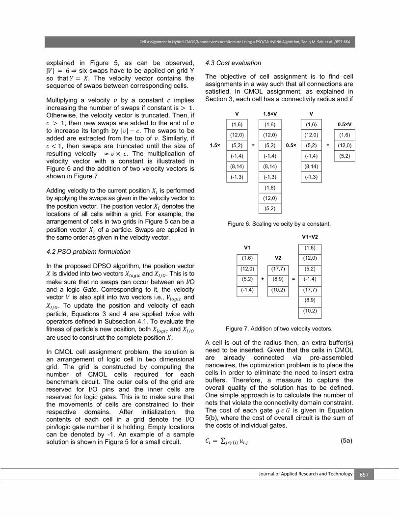
explained in Figure 5, as can be observed, | | = 6 ⇒ six swaps have to be applied on grid Y so that = . The velocity vector contains the sequence of swaps between corresponding cells. Multiplying a velocity by a constant implies increasing the number of swaps if constant is > 1. Otherwise, the velocity vector is truncated. Then, if > 1, then new swaps are added to the end of to increase its length by | | − . The swaps to be added are extracted from the top of . Similarly, if < 1, then swaps are truncated until the size of resulting velocity ≈ × . The multiplication of velocity vector with a constant is illustrated in Figure 6 and the addition of two velocity vectors is shown in Figure 7. Adding velocity to the current position is performed by applying the swaps as given in the velocity vector to the position vector. The position vector denotes the locations of all cells within a grid. For example, the arrangement of cells in two grids in Figure 5 can be a position vector of a particle. Swaps are applied in the same order as given in the velocity vector. 4.2 PSO problem formulation In the proposed DPSO algorithm, the position vector
is divided into two vectors and / . This is to make sure that no swaps can occur between an I/O and a logic Gate. Corresponding to it, the velocity vector is also split into two vectors i.e., and / . To update the position and velocity of each particle, Equations 3 and 4 are applied twice with operators defined in Subsection 4.1. To evaluate the fitness of particle’s new position, both and / are used to construct the complete position . In CMOL cell assignment problem, the solution is an arrangement of logic cell in two dimensional grid. The grid is constructed by computing the number of CMOL cells required for each benchmark circuit. The outer cells of the grid are reserved for I/O pins and the inner cells are reserved for logic gates. This is to make sure that the movements of cells are constrained to their respective domains. After initialization, the contents of each cell in a grid denote the I/O pin/logic gate number it is holding. Empty locations can be denoted by -1. An example of a sample solution is shown in Figure 5 for a small circuit.
4.3 Cost evaluation The objective of cell assignment is to find cell assignments in a way such that all connections are satisfied. In CMOL assignment, as explained in Section 3, each cell has a connectivity radius and if
V 1.5×V V
(1,6) (1,6) (1,6) 0.5×V
(12,0) (12,0) (12,0) (1,6)
1.5× (5,2) = (5,2) 0.5× (5,2) = (12,0)
(-1,4) (-1,4) (-1,4) (5,2)
(8,14) (8,14) (8,14)
(-1,3) (-1,3) (-1,3)
(1,6)
(12,0)
(5,2)
Figure 6. Scaling velocity by a constant.
V1+V2
V1 (1,6)
(1,6) V2 (12,0)
(12,0) (17,7) (5,2)
(5,2) + (8,9) = (-1,4)
(-1,4) (10,2) (17,7)
(8,9)
(10,2)
Figure 7. Addition of two velocity vectors.
A cell is out of the radius then, an extra buffer(s) need to be inserted. Given that the cells in CMOL are already connected via pre-assembled nanowires, the optimization problem is to place the cells in order to eliminate the need to insert extra buffers. Therefore, a measure to capture the overall quality of the solution has to be defined. One simple approach is to calculate the number of nets that violate the connectivity domain constraint. The cost of each gate is given in Equation 5(b), where the cost of overall circuit is the sum of the costs of individual gates. = ∑ ,( ) (5a)
Cell Assignment in Hybrid CMOS/Nanodevices Architecture Using a PSO/SA Hybrid Algorithm, Sadiq M. Sait et al./653‐664
Vol. 11, October 2013 658
, = 1 , >0 ℎ (5b)
4.4 Particle’s evolution Each particle is randomly initialized with a unique solution. The best solution achieved by a particle during the course of iterations is its personal best solution. Global best solution is a best solution among the personal best solutions of all particles. Therefore, initially, each particle will have a different cost value. To change its position, each particle will either increase or decrease its velocity (number of swaps) in order to non-deterministically get closer to its personal best and the global best solution. As illustrated, the velocity in our case is the number of swaps required by a particle to move from one state to the other. Because the problem at hand requires the cells to be placed within each other’s connectivity radius before making any swap, cost will be evaluated, as mentioned in Subsection 4.3, before and after the swap. If the cost is improved or in case the new cost is the same as the previous one, then if overall Manhattan distance is reduced swap is performed, otherwise, it will not. This way, only those swaps that will improve the cost function are made and others are ignored. The intrinsic greedy nature of PSO algorithms allow them to converge very quickly, which may lead to local minima entrapment. Moreover, the PSO algorithm lacks the individual learning capability based on the fitness score of each cell. To address this simulated annealing (SA),-based local search algorithm is employed. SA has been used for a variety of problems and has its strength in the simplicity of its implementation. If SA is run for very long time, then it will give an optimal solution. In this algorithm number of random swaps between I/Os or logic gates for each particle’s solution are performed. To avoid local minima, the SA algorithm will accept a solution of
increased cost with probability ∆ . The initial
temperature is set to be 1.2. The cooling process is implemented using the relation = . The value of is fixed at 0.9. 4.5 An illustrative example Let us consider an example of a simple benchmark circuit to elaborate the working principle of the
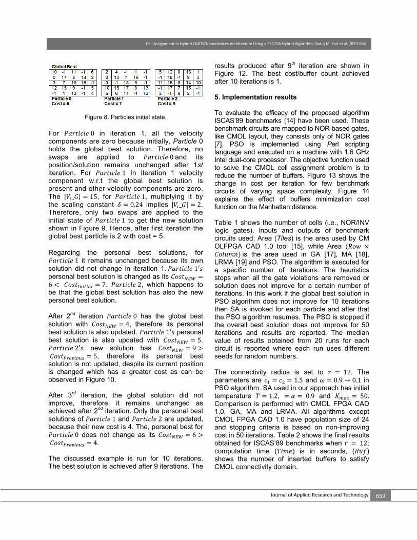
proposed algorithm. For the sake of simplicity, our example has the following parameters, No. of Particles = 3, = = 1.5, = 0.2 and connectivity radius = 3. The considered circuit s27.blif has Total Gates = 19, Logic Gates = 11, I/O Gates = 8 and Grid Size = 5 × 5. The abbreviations used in the example are shown below along their definitions. , : Previous velocity vector of particle , computed using × from Equation 3. _ : Personal best velocity vector of particle computed using − ( ) from Equation 3. _ : Global best velocity vector among all particles computed using − ( ) from Equation 3.
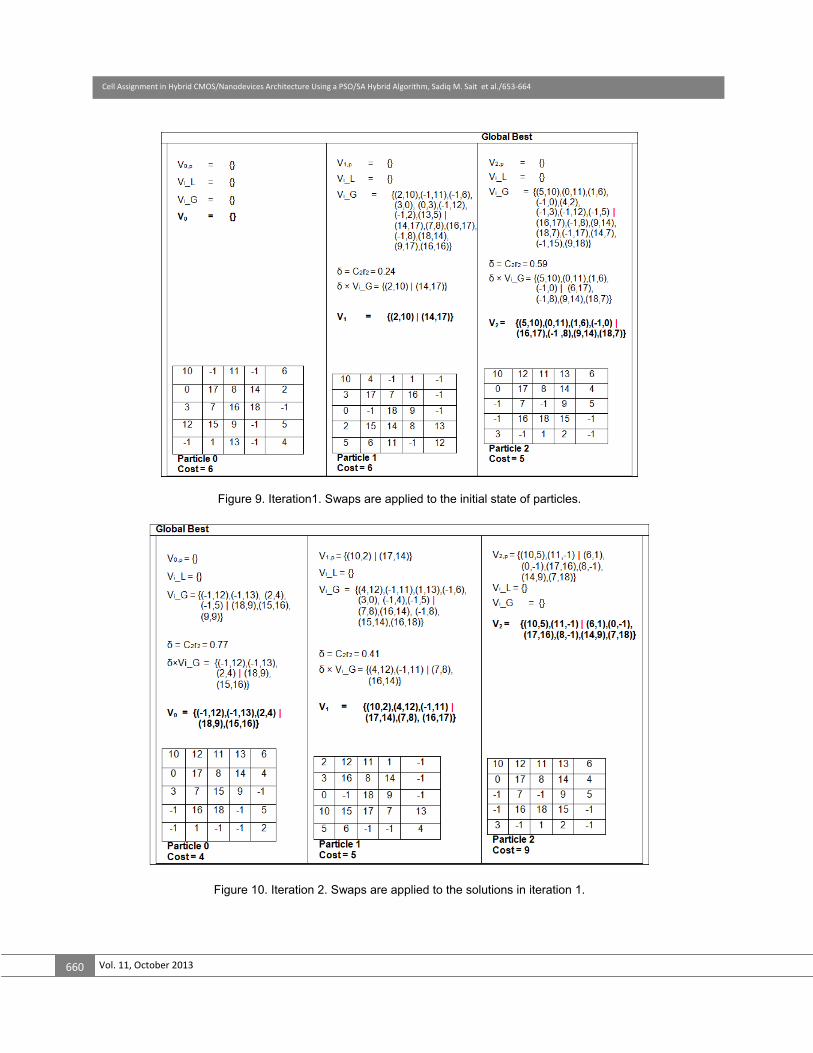
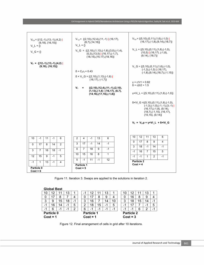
: , + _ + _ from Equation 3. × : Velocity Scaling Factor1 × : Velocity Scaling Factor2 The state of three particles along their costs is shown in Figure 8. The initial velocities of all the particles are initialized to 0. It can also be observed that after initialization the best particle is 0 and the local best solution of each particle is their current solution. We will now go through a few iterations to see how the particles evolve. _ is a set of swaps that are required by a particle to move from its current position to its local best position. _ is a set of swaps that are required by a particle to move from its current position to the global best position. _ and _ are scaled by × and × , respectively so that the new position may lie somewhere between particle’s own best solution and the global best solution, which helps in exploiting the current and exploring the new solutions. Initially, | _ | = , = | _ | = 0 for all particles. After first iteration the particle’s state is shown in Figure 9. The I/O swaps and logic swaps are separated by “|” in the velocity vectors. The solutions shown in Figure 9 are obtained by applying the swaps to the initial state of particles. Similarly, the solutions in Figure 10 were computed by applying the swaps mentioned before to the grids of Figure 9.
Cell Assignment in Hybrid CMOS/Nanodevices Architecture Using a PSO/SA Hybrid Algorithm, Sadiq M. Sait et al. /653‐664
Journal of Applied Research and Technology 659
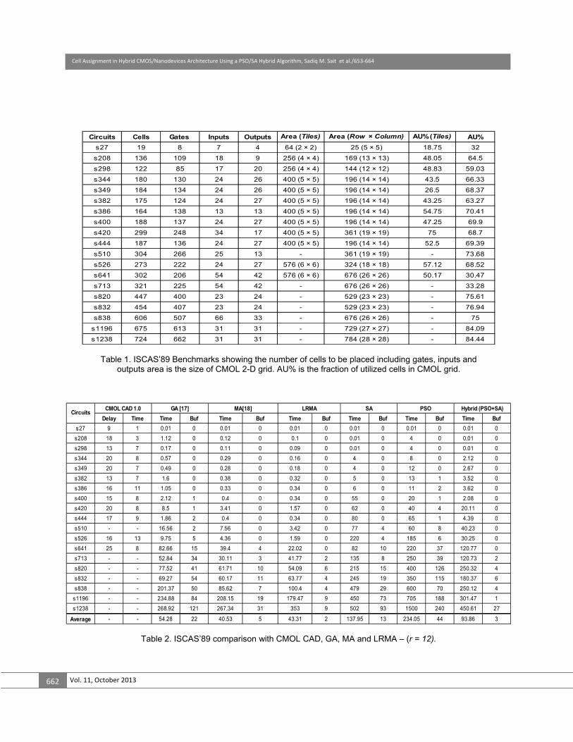
Figure 8. Particles initial state. For 0 in iteration 1, all the velocity components are zero because initially, Particle 0 holds the global best solution. Therefore, no swaps are applied to 0 and its position/solution remains unchanged after 1st iteration. For 1 In iteration 1 velocity component w.r.t the global best solution is present and other velocity components are zero. The | _ | = 15, for 1, multiplying it by the scaling constant = 0.24 implies | _ | = 2. Therefore, only two swaps are applied to the initial state of 1 to get the new solution shown in Figure 9. Hence, after first iteration the global best particle is 2 with cost = 5. Regarding the personal best solutions, for 1 it remains unchanged because its own solution did not change in iteration 1. 1′ personal best solution is changed as its =6 < = 7. 2, which happens to be that the global best solution has also the new personal best solution. After 2nd iteration 0 has the global best solution with = 4, therefore its personal best solution is also updated. 1′ personal best solution is also updated with = 5. 2′ new solution has = 9 > = 5, therefore its personal best solution is not updated, despite its current position is changed which has a greater cost as can be observed in Figure 10. After 3rd iteration, the global solution did not improve, therefore, it remains unchanged as achieved after 2nd iteration. Only the personal best solutions of 1 and 2 are updated, because their new cost is 4. The, personal best for 0 does not change as its = 6 > = 4. The discussed example is run for 10 iterations. The best solution is achieved after 9 iterations. The
results produced after 9th iteration are shown in Figure 12. The best cost/buffer count achieved after 10 iterations is 1. 5. Implementation results To evaluate the efficacy of the proposed algorithm ISCAS’89 benchmarks [14] have been used. These benchmark circuits are mapped to NOR-based gates, like CMOL layout, they consists only of NOR gates [7]. PSO is implemented using Perl scripting language and executed on a machine with 1.6 GHz Intel dual-core processor. The objective function used to solve the CMOL cell assignment problem is to reduce the number of buffers. Figure 13 shows the change in cost per iteration for few benchmark circuits of varying space complexity. Figure 14 explains the effect of buffers minimization cost function on the Manhattan distance. Table 1 shows the number of cells (i.e., NOR/INV logic gates), inputs and outputs of benchmark circuits used; Area (Tiles) is the area used by CM OLFPGA CAD 1.0 tool [15], while Area ( ×) is the area used in GA [17], MA [18], LRMA [19] and PSO. The algorithm is executed for a specific number of iterations. The heuristics stops when all the gate violations are removed or solution does not improve for a certain number of iterations. In this work if the global best solution in PSO algorithm does not improve for 10 iterations then SA is invoked for each particle and after that the PSO algorithm resumes. The PSO is stopped if the overall best solution does not improve for 50 iterations and results are reported. The median value of results obtained from 20 runs for each circuit is reported where each run uses different seeds for random numbers. The connectivity radius is set to = 12. The parameters are = = 1.5 and = 0.9 → 0.1 in PSO algorithm. SA used in our approach has initial temperature = 1.2, = = 0.9 and = 50. Comparison is performed with CMOL FPGA CAD 1.0, GA, MA and LRMA. All algorithms except CMOL FPGA CAD 1.0 have population size of 24 and stopping criteria is based on non-improving cost in 50 iterations. Table 2 shows the final results obtained for ISCAS’89 benchmarks when = 12; computation time ( ) is in seconds, ( ) shows the number of inserted buffers to satisfy CMOL connectivity domain.
Cell Assignment in Hybrid CMOS/Nanodevices Architecture Using a PSO/SA Hybrid Algorithm, Sadiq M. Sait et al./653‐664
Vol. 11, October 2013 660
Figure 9. Iteration1. Swaps are applied to the initial state of particles.
Figure 10. Iteration 2. Swaps are applied to the solutions in iteration 1.
Cell Assignment in Hybrid CMOS/Nanodevices Architecture Using a PSO/SA Hybrid Algorithm, Sadiq M. Sait et al. /653‐664
Journal of Applied Research and Technology 661
V0,p = {(12,-1),(13,-1),(4,2) | (9,18), (16,15)} Vi_L = {}
Vi_G = {}
V0 = {(12,-1),(13,-1),(4,2) | (9,18), (16,15)}
10 -1 11 -1 6
0 17 8 14 2
3 7 16 18 -1
12 15 9 -1 5
-1 1 13 -1 4
Particle 0 Cost = 6
V1,p = {(2,10),(12,4),(11,-1) | (16,17), (8,7),(14,16)}
Vi_L = {}
Vi_G = {(2,10),(1,13),(-1,6),(3,0),(-1,4), (0,3),(13,5) | (16,17),(-1,7), (18,15),(15,17),(18,16)}
δ = C2r2 = 0.43
δ × Vi_G = {(2,10),(1,13),(-1,6) | (16,17), (-1,7)}
V1 = {(2,10),(12,4),(11,-1),(2,10), (1,13),(-1,6) | (16,17), (8,7), (14,16),(17,16),(-1,8)}
2 4 -1 13 6
3 17 -1 14 -1
0 7 18 9 -1
10 15 16 8 1
5 -1 11 -1 12
Particle 1 Cost = 5
V2,p = {(5,10),(0,11),(1,6),(-1,0) | (16,17),(-1,8),(9,14),(18,7)}
Vi_L = {(5,10),(0,11),(1,6),(-1,0), (10,5) | (16,17) ,(-1,8), (9,14), (18,7)}
Vi_G = {(5,10),(0,11),(1,6),(-1,0), (-1,3),(-1,5) | (16,17), (-1,8),(9,14),(18,7),(-1,15)}
γ = c1r1 = 0.82 δ = c2r2 = 1.5
γ×Vi_L = {(5,10),(0,11),(1,6),(-1,0)}
δ×Vi_G ={(5,10),(0,11),(1,6),(-1,0), (-1,3),(-1,5),(-1,-1),(3,-1) | (16,17),(-1,8), (9,14), (18,7),(-1,15), (16,17), (15,15), (9,14)}
V2 = V2,p + γ×Vi_L + δ×Vi_G
10 12 11 13 6
0 17 8 9 4
3 18 -1 14 -1
-1 16 7 15 5
-1 -1 1 2 -1
Particle 2 Cost = 4
Figure 11. Iteration 3. Swaps are applied to the solutions in iteration 2.
Global Best 10 12 11 13 1 -1 12 11 13 1 10 12 11 13 1 0 17 8 7 4 0 17 8 9 4 0 16 8 9 4 3 9 15 18 -1 3 16 7 14 10 3 18 15 14 -1 -1 16 14 -1 5 2 18 15 -1 5 -1 17 7 -1 5 -1 6 -1 -1 2 6 -1 -1 -1 -1 -1 -1 6 2 -1 Particle 0 Particle 1 Particle 2 Cost = 1 Cost = 1 Cost = 3
Figure 12. Final arrangement of cells in grid after 10 iterations.
Cell Assignment in Hybrid CMOS/Nanodevices Architecture Using a PSO/SA Hybrid Algorithm, Sadiq M. Sait et al./653‐664
Vol. 11, October 2013 662
Circuits Cells Gates Inputs Outputs Area (Tiles) Area (Row × Column) AU% (Tiles) AU%
s27 19 8 7 4 64 (2 × 2) 25 (5 × 5) 18.75 32
s208 136 109 18 9 256 (4 × 4) 169 (13 × 13) 48.05 64.5
s298 122 85 17 20 256 (4 × 4) 144 (12 × 12) 48.83 59.03
s344 180 130 24 26 400 (5 × 5) 196 (14 × 14) 43.5 66.33
s349 184 134 24 26 400 (5 × 5) 196 (14 × 14) 26.5 68.37
s382 175 124 24 27 400 (5 × 5) 196 (14 × 14) 43.25 63.27
s386 164 138 13 13 400 (5 × 5) 196 (14 × 14) 54.75 70.41
s400 188 137 24 27 400 (5 × 5) 196 (14 × 14) 47.25 69.9
s420 299 248 34 17 400 (5 × 5) 361 (19 × 19) 75 68.7
s444 187 136 24 27 400 (5 × 5) 196 (14 × 14) 52.5 69.39
s510 304 266 25 13 - 361 (19 × 19) - 73.68
s526 273 222 24 27 576 (6 × 6) 324 (18 × 18) 57.12 68.52
s641 302 206 54 42 576 (6 × 6) 676 (26 × 26) 50.17 30.47
s713 321 225 54 42 - 676 (26 × 26) - 33.28
s820 447 400 23 24 - 529 (23 × 23) - 75.61
s832 454 407 23 24 - 529 (23 × 23) - 76.94
s838 606 507 66 33 - 676 (26 × 26) - 75
s1196 675 613 31 31 - 729 (27 × 27) - 84.09
s1238 724 662 31 31 - 784 (28 × 28) - 84.44
Table 1. ISCAS’89 Benchmarks showing the number of cells to be placed including gates, inputs and outputs area is the size of CMOL 2-D grid. AU% is the fraction of utilized cells in CMOL grid.
Delay Time Time Buf Time Buf Time Buf Time Buf Time Buf Time Buf
s27 9 1 0.01 0 0.01 0 0.01 0 0.01 0 0.01 0 0.01 0
s208 18 3 1.12 0 0.12 0 0.1 0 0.01 0 4 0 0.01 0
s298 13 7 0.17 0 0.11 0 0.09 0 0.01 0 4 0 0.01 0
s344 20 8 0.57 0 0.29 0 0.16 0 4 0 8 0 2.12 0
s349 20 7 0.49 0 0.28 0 0.18 0 4 0 12 0 2.67 0
s382 13 7 1.6 0 0.38 0 0.32 0 5 0 13 1 3.52 0
s386 16 11 1.05 0 0.33 0 0.34 0 6 0 11 2 3.62 0
s400 15 8 2.12 1 0.4 0 0.34 0 55 0 20 1 2.08 0
s420 20 8 8.5 1 3.41 0 1.57 0 62 0 40 4 20.11 0
s444 17 9 1.86 2 0.4 0 0.34 0 80 0 65 1 4.39 0
s510 - - 16.56 2 7.56 0 3.42 0 77 4 60 8 40.23 0
s526 16 13 9.75 5 4.36 0 1.59 0 220 4 185 6 30.25 0
s641 25 8 82.66 15 39.4 4 22.02 0 82 10 220 37 120.77 0
s713 - - 52.84 34 30.11 3 41.77 2 135 8 250 39 120.73 2
s820 - - 77.52 41 61.71 10 54.09 6 215 15 400 126 250.32 4
s832 - - 69.27 54 60.17 11 63.77 4 245 19 350 115 180.37 6
s838 - - 201.37 50 85.62 7 100.4 4 479 29 600 70 250.12 4
s1196 - - 234.88 84 208.15 19 179.47 9 450 73 705 188 301.47 1
s1238 - - 268.92 121 267.34 31 353 9 502 93 1500 240 450.61 27
Average - - 54.28 22 40.53 5 43.31 2 137.95 13 234.05 44 93.86 3
Hybrid (PSO+SA)Circuits
CMOL CAD 1.0 GA [17] MA[18] LRMA SA PSO
Table 2. ISCAS’89 comparison with CMOL CAD, GA, MA and LRMA – (r = 12).

Cell Assignment in Hybrid CMOS/Nanodevices Architecture Using a PSO/SA Hybrid Algorithm, Sadiq M. Sait et al. /653‐664
Journal of Applied Research and Technology 663
PSO solutions are more effective than those of CMOL CAD 1.0 in terms of delay and area utilization. The last two columns of Table 1 show that cell-based CMOL architecture has better area utilization % than that of tile-based architecture. Table 2 indicates that the tile-based approach is the most time consuming and the least effective in timing delay, it also fails to place big circuits. The results achieved by hybrid PSO/SA algorithm, as shown in Table 2, are better than GA and MA in terms of number of inserted buffers for all benchmark circuits. It can also be observed that the overall solution quality and computation time by SA and PSO just for larger circuits is not encouraging. Hybrid algorithm produced results that are better in all performance comparison criteria. Comparing to LRMA, better results are achieved in terms of delay and number of inserted buffers for all benchmark circuits except for 832 and 1238, as they require more buffers in the proposed approach. The average time taken by PSO/SA hybrid is more as compared to other techniques due to the compute intensive operations of updating the velocity and position of each particle.
Figure 13. Change in cost per iteration of few benchmarks.
Figure 14. Change in cost and Manhattan distance per iteration of s1196.blif.
6. Conclusions This paper discussed the implementation of a hybrid particle swarm optimization and simulated annealing heuristic for CMOL nano-hybrid cells assignment. The behavior of the problem was analyzed and a technique was engineered that utilized the exploration and exploitation features of PSO to solve the problem. In the proposed algorithm the PSO operators, like velocity and position update were defined in the context of assignment problem. Due to the inherent greedy nature of PSO algorithm, simulated annealing (SA) was used in hybrid to escape local minima entrapment. Implementation results illustrated that the proposed scheme achieved better results for most of the benchmarks as compared to other published techniques in previous studies. Acknowledgments The authors acknowledge King Fahd University of Petroleum & Minerals for all the support, and Dr. William N. N. Hung and Mr. Zhufei Chu for providing ISCAS’89 benchmark files. The authors also would like to thank Mr. Abdalrahman M. Arafeh for his help and support.
References [1] Philip J. Kuekes, Duncan R. Stewart, and R. Stanley Williams. The crossbar latch: logic value storage, restoration, and inversion in crossbar circuits. Journal of Applied Physics, 97:03430115, 2005. [2] D. J. Resnick. Imprint lithography for integrated circuit fabrication. Journal of Vacuum Science & Technology B: Microelectronics and Nanometer Structures, 21:2624, 2003. [3] K. K. Likharev and D. V. Strukov. CMOL: devices, circuits, and architectures. In G Cuniberti et al., editors, Introduction to Molecular Electronics, pages 447477. Springer, Berlin, 2005. [4] Dmitri B. Strukov and Konstantin K. Likharev. CMOL FPGA: a reconfigurable architecture for hybrid digital circuits with two terminal nanodevices. Nanotechnology, 16(6):888900, 2005. [5] Oˆ. Tu¨rel, J. H. Lee, X. Ma, and Konstantin K. Likharev. Architectures for nanoelectronic implementation of artificial neural networks: new results. Neurocomputing, 64:271283, 2005. [6] D. Strukov and K. Likharev. A reconfigurable architecture for hybrid CMOS/nanodevice circuits. In FPGA06, pages 131140, Monterey, California, USA, 2006.
Cell Assignment in Hybrid CMOS/Nanodevices Architecture Using a PSO/SA Hybrid Algorithm, Sadiq M. Sait et al./653‐664
Vol. 11, October 2013 664
[7] William N. N. Hung, Changjian Gao, Xiaoyu Song, and Dan Hammerstrom. Defect Tolerant CMOL Cell Assignment via Satisfiability. IEEE Sensors Journal, 8(6):823830, June 2008. [8] Mohammed El-Abd, Hassan Hassan, Mohab Anis, Mohamed S. Kamel, and Mohamed Elmasry. 2010. Discrete cooperative particle swarm optimization for FPGA assignment. Appl. Soft Computing 10, 1 (January 2010), 284-295. [9] Lim, A., Lin, J., & Xiao, F. (2007). Particle Swarm Optimization and Hill Climbing for the bandwidth minimization problem. Applied Intelligence, 26(3), 175-182. [10] F. Glover, J. P. Kelly, and M. Laguna. Genetic algorithms and tabu search: Hybrids for optimization. Computers and Operations Research, 22(1):111–134, 1995. [11] Sait, S.M., Youssef, H.: Iterative Computer Algorithms with Applications in Engineering: Solving Combinatorial Optimization Problems. IEEE Computer Society Press, California (1999). [12] J. Kennedy, R.C. Eberhart, Particle swarm optimization, in: Proceedings of the IEEE International Conference on Neural Networks, vol. 4, 1995, pp. 19421948. [13] Kennedy, J.; Eberhart, R.C.”A discrete binary version of the particle swarm algorithm”, IEEE International Conference on Systems, Man, and Cybernetics, 1997. [14] Brglez, F., Bryan, D., Kozminski, K.: Combinational profiles of sequential benchmark circuits. In: Circuits and Systems, 1989, IEEE International Symposium on, pp. 1929 1934 vol.3 (1989). DOI 10.1109/ISCAS.1989.100747. [15] Strukov, D.B., Likharev, K.K.: A reconfigurable architecture for hybrid CMOS/Nanodevice circuits. In: Proceedings of the 2006. ACM/SIGDA 14th international symposium on Field programmable gate arrays, FPGA 06, pp. 131140. ACM, New York, NY, USA (2006). [16] Andrew Lim, Jing Lin, and Fei Xiao. 2007. Particle Swarm Optimization and Hill Climbing for the bandwidth minimization problem. Applied Intelligence 26, 3 (June 2007), 175-182. DOI=10.1007/s10489-006-0019-x http://dx.doi.org/10.1007/s10489-006-0019-x. [17] Xia Y., Chu Z., Hung, W. N., Wang, L., Song, X.: CMOL cell assignment by genetic algorithm. In: NEWCAS Conference (NEWCAS), 2010 8th IEEE International, pp. 25 28 (2010). DOI 10.1109/NEWCAS.2010.5603746.
[18] Chu Z., Xia Y., Hung, W.N., Wang L., Song X.: A memetic approach for nanoscale hybrid circuit cell mapping. In: Digital System Design: Architectures, Methods and Tools (DSD), 2010 13th Euromicro Conference on, pp. 681 688 (2010). DOI 10.1109/DSD.2010.22. [19] Xia Y., Chu Z., Hung W., Wang L., Song,X.: An integrated optimization approach for nano-hybrid circuit cell mapping. Nanotechnology, IEEE Transactions on PP (99), 1 (2011). DOI 10.1109/TNANO.2011.2131153. [20] A. E. Ylmaz F. Yaman. Impacts of genetic algorithm parameters on the solution performance for the uniform circular antenna array pattern synthesis problem. Journal of Applied Research and Technology, 8(3):378-394, December, 2010. [21] Nareli Cruz-Cortes Ricardo Barron-Fernandez Jesus A. Alvarez-Cedillo Gerardo A. Laguna-Sanchez, Mauricio Olguin-Carbajal. Comparative study of parallel variants for a particle swarm optimization algorithm implemented on a multithreading GPU. Journal of Applied Research and Technology, 7(3):292-309, December, 2009. [22] A. Miranda-Vitela F. Lara-Rosano J. L. Perez-Silva, A. Garces-Madrigal. Dynamic fuzzy logic functor. Journal of Applied Research and Technology, 6(2):84-94, August, 2008.