CECAM – Workshoppsi-k.net/wp-content/uploads/2018/10/CECAM-Qubit... · 2018-10-03 · Program of...
74
CECAM – Workshop Crystal defects for qubits single photon emitters and nanosensors July 9 th – 13 th 2018 Bremen Center for Computational Materials Science University of Bremen
Transcript of CECAM – Workshoppsi-k.net/wp-content/uploads/2018/10/CECAM-Qubit... · 2018-10-03 · Program of...
CECAM – Workshop
Crystal defects for qubits single photon emitters and nanosensors
July 9th – 13th 2018
Bremen Center for Computational Materials Science
University of Bremen

Program of the International CECAM-Workshop Crystal defects for qubits, single photon emitters and nanosensors
Bremen Center for Computational Materials Science – BCCMS University of Bremen, July 9th - 13th 2018
Conference site: House of Science, Downtown
1
Tuesday, July 10th 2018 (House of Science Bremen, Downtown)
08:00 – 08:50 Registration 08:50 – 09:00 Opening and welcome, Thomas Frauenheim Session: Quantum defects for qubits Chair: Thomas Frauenheim 09:00 – 09:40 Jörg Wrachtrup, University of Stuttgart, Germany
Applying single solid state quantum defects 09:40 – 10:20 David D. Awschalom, The University of Chicago, Illinois, USA
Controlling defect spin states with photons, magnons, and phonons
10:20 – 10:45 Coffee Break 10:45 – 11:25 Ádám Gali, Wigner Research Centre for Physics, Hungarian Academy of
Sciences, Budapest, Hungary Toward full ab initio description of qubits in solids
Session: Spin states Chair: Peter Deák 11:25 – 12:05 Fedor Jelezko, Ulm University, Germany
Photoelectrical readout of single spins in diamond 12:05 – 12:45 Ronald Hanson, Delft University of Technology, The Netherlands
The dawn of quantum networks 12:45 Group photo 12:50 – 14:15 Lunch Break (Restaurant Stadtwirt) and Coffee 14:15 – 14:55 Martin B. Plenio, Ulm University, Germany
Controlling nuclear spin registers by NV- centers Session: Quantum spintronics Chair: Michael Lorke 14:55 – 15:35 Mike J. Ford, University of Technology Sydney, New South Wales,
Australia Evaluating electronic structure calculations of single photon emitting defects in hBN
15:35 – 16:00 Coffee Break 16:00 – 16:40 Marcus W. Doherty, Australian National University, Canberra, Australia
Quantum spintronic properties of diamond nanowires
16:40 – 17:20 Jeronimo R. Maze, Pontifical Catholic University of Chile, Santiago Effect of phonons on individual electronic spin relaxation and electron spin resonance
18:00 – 20:30 Welcome Reception (Bremen Town Hall)

Program of the International CECAM-Workshop Crystal defects for qubits, single photon emitters and nanosensors
Bremen Center for Computational Materials Science – BCCMS University of Bremen, July 9th - 13th 2018
Conference site: House of Science, Downtown
2
Wednesday, July 11th 2018 (House of Science Bremen, Downtown)
Session: Quantum probes and quantum control Chair: Joerg Wrachtrup 09:00 – 09:40 Gavin W. Morley, University of Warwick, Coventry, UK
Levitating nanodiamonds containing NV- centers
09:40 – 10:20 John J. L. Morton, University College London, UK Strain effects on donor spins in silicon
10:20 – 10:50 Coffee Break 10:50 – 11:30 Alex Retzker, The Hebrew University of Jerusalem, Israel
Limits on spectral resolution measurements by quantum probes for nano NMR
11:30 – 12:10 Vladimir Dyakonov, University of Würzburg, Germany Engineering of highly coherent vacancy spins in SiC
12:10 – 12:50 Viktor Ivády, Wigner Research Centre for Physics, Hungarian Academy of Sciences, Budapest, Hungary Novel ab initio and model spin Hamiltonian methods for spin dynamic simulations of point defect quantum bits
12:50 – 14:30 Lunch Break (Restaurant Stadtwirt) and Coffee Session: Interactions with photons Chair: Ádám Gali 14:30 – 15:10 Sophia Economou, Virginia Polytechnic Institute and State University,
Blacksburg, Virginia, USA Spin-photon interfaces for graph generation based on defects in diamond and SiC
15:10 – 15:50 Michel Bockstedte, University of Salzburg, Austria Spin and photo physics of prototypical defect centers in diamond and SiC
15:50 – 16:20 Coffee Break 16:20 – 17:00 Brett C. Johnson, The University of Melbourne, Victoria, Australia
Silicon carbide single photon source devices
17:00 – 17:40 Christoph Becher, Saarland University, Saarbrücken, Germany Spin properties and quantum control of Si vacancy centers in diamond
18:40 Bus Pickup to Conference Dinner (Venue: Radisson Blu Hotel, Wachtstraße)
19:00 – 22:30 Conference Dinner (Restaurant Juergenshof)

Program of the International CECAM-Workshop Crystal defects for qubits, single photon emitters and nanosensors
Bremen Center for Computational Materials Science – BCCMS University of Bremen, July 9th - 13th 2018
Conference site: House of Science, Downtown
3
Thursday, July 12th 2018 (House of Science Bremen, Downtown)
Session: Defect control and qubits Chair: Tim Wehling 09:00 – 09:40 Nguyen Tien Son, Linköping University, Sweden
Electron paramagnetic resonance studies of silicon vacancy in isotopically purified SiC
09:40 – 10:20 Lee C. Bassett, University of Pennsylvania, Philadelphia, USA Optically addressable spin defects in hexagonal boron nitride
10:20 – 10:50 Coffee Break Chair: Andreia Luisa da Rosa 10:50 – 11:30 Uwe Gerstmann, Paderborn University, Germany
Magneto-optical properties of NV- centers in SiC: how relativistic effects trigger spin-based qubits
11:30 – 12:10 Kai-Mei C. Fu, University of Washington, Seattle, USA Shallow impurities in ZnO for quantum information applications
12:10 – 12:50 Hosung Seo, Ajou University, Suwon, South Korea Computational design of new point defects in semiconductors for qubit applications
12:50 – 14:30 Lunch Break (Restaurant Stadtwirt) and Coffee Session: Experimental characterization of interfaces Chair: Jean-Marie Bluet 14:30 – 15:10 Shengbai Zhang, Rensselaer Polytechnic Institute, Troy, New York,
USA Dynamic Jahn -Teller effect of the NV- center in diamond and beyond
15:10 - 15:50 Arne Laucht, University of New South Wales, Sydney, Australia Donor spin qubits in Si: from single-shot readout to advanced control methods
17:20 Poster Mounting 17:30 – 20:30 Poster Session, Catering Buffet (House of Science)
Program of the International CECAM-Workshop Crystal defects for qubits, single photon emitters and nanosensors
Bremen Center for Computational Materials Science – BCCMS University of Bremen, July 9th - 13th 2018
Conference site: House of Science, Downtown
4
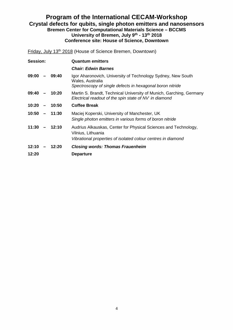
Friday, July 13th 2018 (House of Science Bremen, Downtown)
Session: Quantum emitters Chair: Edwin Barnes 09:00 – 09:40 Igor Aharonovich, University of Technology Sydney, New South
Wales, Australia Spectroscopy of single defects in hexagonal boron nitride
09:40 – 10:20 Martin S. Brandt, Technical University of Munich, Garching, Germany Electrical readout of the spin state of NV- in diamond
10:20 – 10:50 Coffee Break
10:50 – 11:30 Maciej Koperski, University of Manchester, UK Single photon emitters in various forms of boron nitride
11:30 – 12:10 Audrius Alkauskas, Center for Physical Sciences and Technology, Vilnius, Lithuania Vibrational properties of isolated colour centres in diamond
12:10 – 12:20 Closing words: Thomas Frauenheim 12:20 Departure

Abstracts of Lectures
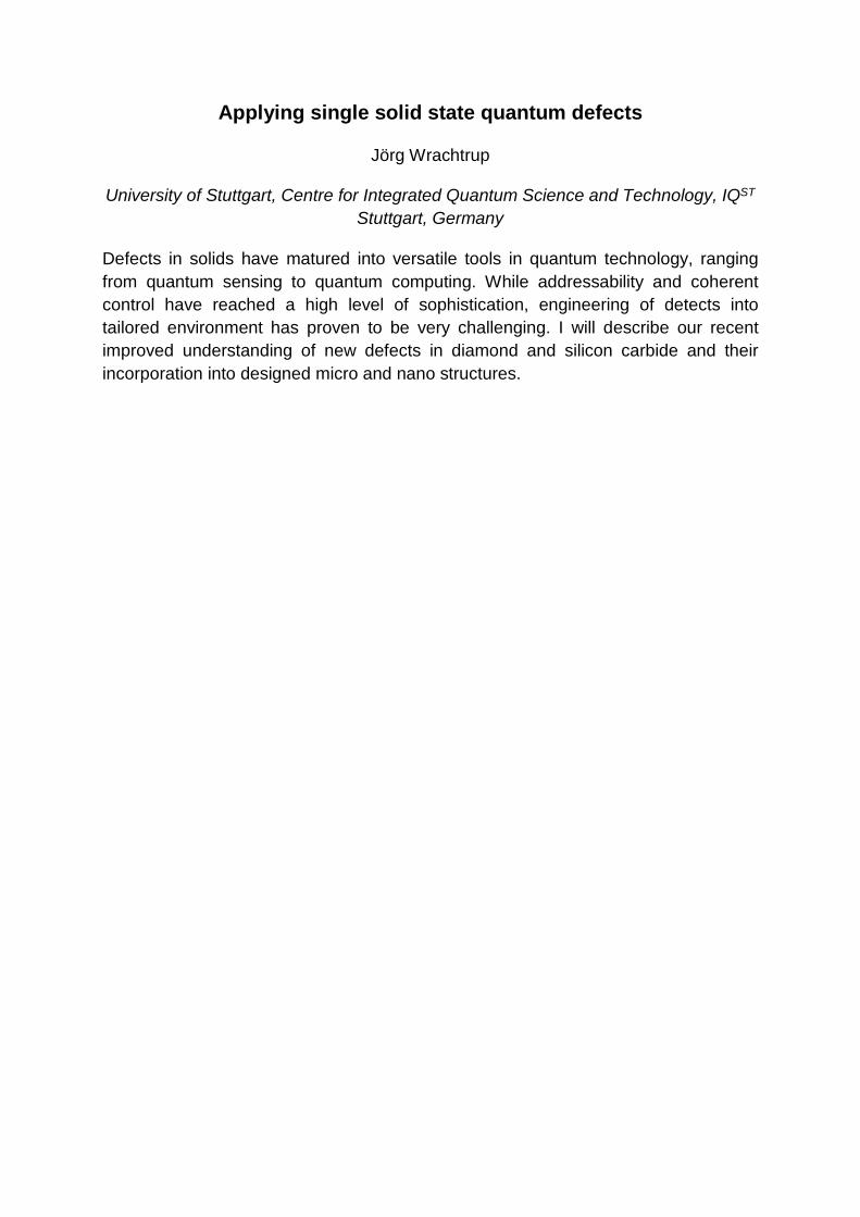
Applying single solid state quantum defects
Jörg Wrachtrup
University of Stuttgart, Centre for Integrated Quantum Science and Technology, IQST Stuttgart, Germany
Defects in solids have matured into versatile tools in quantum technology, ranging from quantum sensing to quantum computing. While addressability and coherent control have reached a high level of sophistication, engineering of detects into tailored environment has proven to be very challenging. I will describe our recent improved understanding of new defects in diamond and silicon carbide and their incorporation into designed micro and nano structures.
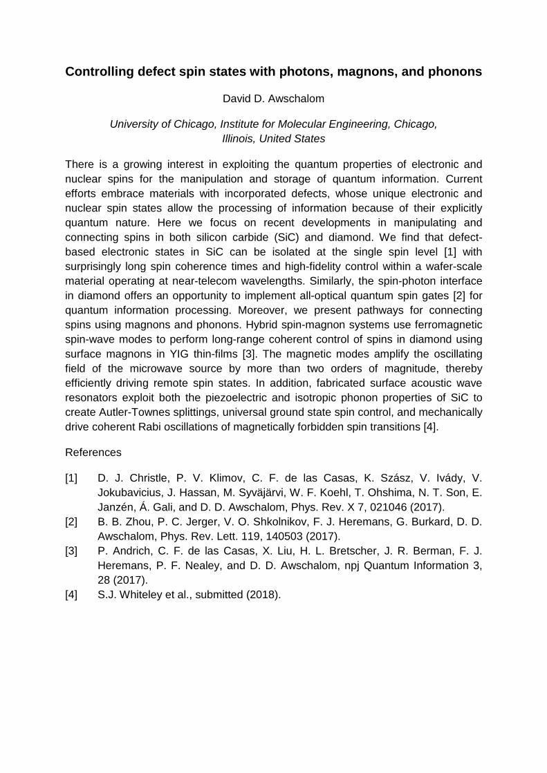
Controlling defect spin states with photons, magnons, and phonons
David D. Awschalom
University of Chicago, Institute for Molecular Engineering, Chicago, Illinois, United States
There is a growing interest in exploiting the quantum properties of electronic and nuclear spins for the manipulation and storage of quantum information. Current efforts embrace materials with incorporated defects, whose unique electronic and nuclear spin states allow the processing of information because of their explicitly quantum nature. Here we focus on recent developments in manipulating and connecting spins in both silicon carbide (SiC) and diamond. We find that defect-based electronic states in SiC can be isolated at the single spin level [1] with surprisingly long spin coherence times and high-fidelity control within a wafer-scale material operating at near-telecom wavelengths. Similarly, the spin-photon interface in diamond offers an opportunity to implement all-optical quantum spin gates [2] for quantum information processing. Moreover, we present pathways for connecting spins using magnons and phonons. Hybrid spin-magnon systems use ferromagnetic spin-wave modes to perform long-range coherent control of spins in diamond using surface magnons in YIG thin-films [3]. The magnetic modes amplify the oscillating field of the microwave source by more than two orders of magnitude, thereby efficiently driving remote spin states. In addition, fabricated surface acoustic wave resonators exploit both the piezoelectric and isotropic phonon properties of SiC to create Autler-Townes splittings, universal ground state spin control, and mechanically drive coherent Rabi oscillations of magnetically forbidden spin transitions [4].
References
[1] D. J. Christle, P. V. Klimov, C. F. de las Casas, K. Szász, V. Ivády, V. Jokubavicius, J. Hassan, M. Syväjärvi, W. F. Koehl, T. Ohshima, N. T. Son, E. Janzén, Á. Gali, and D. D. Awschalom, Phys. Rev. X 7, 021046 (2017).
[2] B. B. Zhou, P. C. Jerger, V. O. Shkolnikov, F. J. Heremans, G. Burkard, D. D. Awschalom, Phys. Rev. Lett. 119, 140503 (2017).
[3] P. Andrich, C. F. de las Casas, X. Liu, H. L. Bretscher, J. R. Berman, F. J. Heremans, P. F. Nealey, and D. D. Awschalom, npj Quantum Information 3, 28 (2017).
[4] S.J. Whiteley et al., submitted (2018).
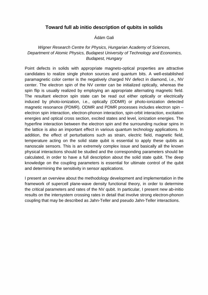
Toward full ab initio description of qubits in solids
Ádám Gali
Wigner Research Centre for Physics, Hungarian Academy of Sciences, Department of Atomic Physics, Budapest University of Technology and Economics,
Budapest, Hungary
Point defects in solids with appropriate magneto-optical properties are attractive candidates to realize single photon sources and quantum bits. A well-established paramagnetic color center is the negatively charged NV defect in diamond, i.e., NV center. The electron spin of the NV center can be initialized optically, whereas the spin flip is usually realized by employing an appropriate alternating magnetic field. The resultant electron spin state can be read out either optically or electrically induced by photo-ionization, i.e., optically (ODMR) or photo-ionization detected magnetic resonance (PDMR). ODMR and PDMR processes includes electron spin – electron spin interaction, electron-phonon interaction, spin-orbit interaction, excitation energies and optical cross section, excited states and level, ionization energies. The hyperfine interaction between the electron spin and the surrounding nuclear spins in the lattice is also an important effect in various quantum technology applications. In addition, the effect of perturbations such as strain, electric field, magnetic field, temperature acting on the solid state qubit is essential to apply these qubits as nanoscale sensors. This is an extremely complex issue and basically all the known physical interactions should be studied and the corresponding parameters should be calculated, in order to have a full description about the solid state qubit. The deep knowledge on the coupling parameters is essential for ultimate control of the qubit and determining the sensitivity in sensor applications.
I present an overview about the methodology development and implementation in the framework of supercell plane-wave density functional theory, in order to determine the critical parameters and rates of the NV qubit. In particular, I present new ab-initio results on the intersystem crossing rates in detail that involve strong electron-phonon coupling that may be described as Jahn-Teller and pseudo Jahn-Teller interactions.
Photoelectrical readout of single spins in diamond
Fedor Jelezko
Ulm University, Institute of Quantum Optics, Ulm, Germany
Color centers in diamond are promising for wide range of technology applications including quantum information processing quantum communicating and quantum sensing. Most of results obtained so far with nitrogen vacancy (NV) centers are based on optical detection of single NV color centers. In this talk, we will show that photoelectrical detection of NV centers base on spin selective photoionization can provide robust and efficient access to spin state of individual NV centers.
The dawn of quantum networks
Ronald Hanson
Delft University of Technology, QuTech and Kavli Institute of Nanoscience, Delft, The Netherlands
Entanglement – the property that particles can share a single quantum state - is arguably the most counterintuitive yet potentially most powerful element in quantum theory. The non-local features of quantum theory are highlighted by the conflict between entanglement and local causality discovered by John Bell. Decades of Bell inequality tests, culminating in a series of loophole-free tests in 2015, have confirmed the non-local of nature. Future quantum networks may harness these unique features of entanglement in a range of exciting applications, such as quantum computation and simulation, secure communication, enhanced metrology for astronomy and time-keeping as well as fundamental investigations. To fulfill these promises, a strong worldwide effort is ongoing to gain precise control over the full quantum dynamics of multi-particle nodes and to wire them up using quantum-photonic channels. Diamond spins associated with NV centers are promising building blocks for such a network as they combine a coherent electron-optical interface [1] (similar to that of trapped atomic qubits) with a local register of robust and well-controlled nuclear spin qubits [2]. Here I will introduce the field of quantum networks and discuss future plans and ongoing work with the specific target of realizing the first multi-node network wired by quantum entanglement, including first primitive network experiments [3,4].
References
[1] W. Pfaff et al., Science 345, 532 (2014); B. Hensen et al., Nature 526, 682 (2015). [2] J. Cramer et al., Nature Comm. 7, 11526 (2016). [3] N. Kalb et al., Science 356, 928 (2017). [4] P.C. Humphreys et al., https://arxiv.org/abs/1712.07567.
Controlling nuclear spin registers by NV centers
Martin B. Plenio
Ulm University, Institute of Theoretical Physics, Ulm, Germany
In this lecture I will present a variety of robust and efficient schemes for the control of nuclear spin registers by means of a single NV center. Applications will range from uantum information processing to polarisation of nuclear spins.

Evaluating electronic structure calculations of single photon emitting defects in hBN
A. Sajid, S. A. Tawfik, M. Fronzi, R. Kobayashi, J. R. Reimers and M. J. Ford
University of Technology, School of Mathematical and Physical Sciences, Sydney, Australia
University of Faisalabad, Punjab, Pakistan Shanghai University, International Centre for Quantum and Molecular Structures,
Shanghai, China The Australian National University, 4NCI, Canberra, Australia
Flinders University of South Australia, Adelaide, Australia
Defect states in 3D, and more recently 2D, crystals are promising sources of single photons for a variety of quantum technologies. The NV- defect in bulk and nano-diamond [1] is perhaps the most widely studied of these. Understanding the spectroscopy of these defects states is a considerable challenge and requires advances in both the experimental and theoretical domains. To date, the most widely used approach to this problem computationally is to use Density Functional Theory based methods offering a good balance between computational expediency and reliability. The HSE06 functional reproduces bandgaps in semiconductors well and, combined with methods to constrain orbital occupation, is perhaps the most favoured approach for calculating defect excited states. Many of the electronic states for these defects, however, are inherently multi-reference open-shell and closed-shell states and involve broken chemical bonds and charge-transfer states.
In this presentation we evaluate the performance of DFT methods by benchmarking against high level coupled-cluster and multi-reference methods with particular application to monolayer hexagonal boron nitride. The recent discovery of single-photon emission from this material [2] has generated considerable interest and efforts are underway to characterise the spectroscopy of this emission [3,4,5]. We find that some DFT methods can perform very poorly, for example PBE. HSE06 works well for excitations among the triplet states but underestimates triplets relative to closed-shell singlets, and fails with regard to open-shell singlet states. Long-range corrected functionals such as CAM-B3LYP perform much better, but their implementations so far have been restricted to non-periodic codes. We also show that there can be significant differences between cluster and periodic-slab models of these defects implying that implementation of such functionals in periodic codes is needed.
This work was supported by resources provided by the National Computational Infrastructure (NCI), and Pawsey Supercomputing Centre with funding from the Australian Government and the Government of Western Australia, as well as Chinese NSF Grant #1167040630. SA acknowledges receipt of an Australian Postgraduate Award funded by ARC DP 150103317. Funded is also acknowledged from ARC DP 160101301.
References
[1] For example, M W Doherty, N B Manson, P Delaney, F Jelezko, J Wrachtrup, L C L Hollenberg, Phys Rep 528(1) 1 (2013)
[2] T T Tran, K Bray, M J Ford, M Toth, I Aharonovich, Nature Nanotech, 11 37-41(2016)
[3] M Abdi, J-P Chou, A Gali, M B Plenio, arxiv:1709.05414v1 (2017); M Abdi, M-J Hwang, M Aghtar, M B Plenio, Phys Rev Letts 119 233602 (2017); F Wu, A Galatas, R Sundararaman, D Rocca, Y Ping, Phys Rev Materials, 1 071001(R) (2017)
[4] S A Tawfik, S Ali, M Fronzi, M Kiannia, T T Tran, C Stampfl, I Aharonovich, M Toth, M J Ford, Nanoscale 9(36) 13575 (2017);
[5] A Sajid, Jeffrey R Reimers, Michael J Ford, Phys Rev B DOI:10.1103/PhysRevB.97.064101 (2018); J Reimers, S Ali, M Ford, J Chem Theory and Comp DOI: 10.1021/acs.jctc.7b01072 (2018)
Quantum spintronic properties of diamond nanowires
L. Oberg (1), E. Huang (1), A. Alkauskas (2), C.A. Meriles (3), N. B. Manson (1) M. W. Doherty (1)
(1) Australian National University, Canberra, Laser Physics Centre, Research School of Physics and Engineering, Canberra, Australia
(2) CUNY-City College of New York, Department of Physics, New York, United States
(3) Center for Physical Sciences and Technology, Vilnius, Lithuania
A major barrier to large-scale diamond quantum computing is the realisation of an on-chip quantum bus capable of entangling the spins of different NV centers. There have been various quantum bus designs proposed, and these may be summarised by their mediation of entanglement by either photons, phonons, magnons or defect spin chains. As yet, entanglement has only been successfully demonstrated via the exchange of photons between distant NV centers and the direct spin-spin coupling of neighbouring NV centers. Both approaches face major difficulties in scaling, reaching sufficient entanglement generation rates and fidelity. Thus, the identification of a scalable on-chip quantum bus is still an open question in diamond quantum computing. We recently proposed a very different approach to an on-chip quantum bus: the spin-coherent transport of electrons between NV centers. This approach seeks to exploit the naturally extreme spin transport properties of diamond as well as the well-developed techniques to optically manipulate defect charge states. In our proposal, we identified that the electron transport must be confined within diamond nanowires. However, the precise influence of the nanowire geometry on diamond’s spin transport properties was a question left unanswered. In this presentation, we will report our latest first-principles calculations of the spin transport properties of diamond nanowires and our assessment of how they permit novel techniques for semi-classical and quantum transport of electron spins between NV centers.

Effect of phonons on individual electronic spin relaxation and electron spin resonance
J. R. Maze (1,2), A. Norambuena (1,2), E. Muñoz (1,2), H. Dinani (1), A. Jarmola (3), P. Maletinsky (4), D. Budker (3,5,6), C. Becher (7)
(1) Pontifical Catholic University of Chile, Institute of Physics, Santiago, Chile (2) Pontifical Catholic University of Chile, Center for Nanotechnology and
Advanced Materials, Santiago, Chile (3) University of California, Department of Physics,
Berkeley, California, United States (4) University of Basel, Department of Physics, Basel, Switzerland
(5) Johannes Gutenberg University, Helmholtz Institute, Mainz, Germany (6) Lawrence Berkeley National Laboratory, Nuclear Science Division,
Berkeley, California, Unites States (7) Saarland University, Department of Physics, Saarbrücken, Germany
Understanding the effect of temperature on the relaxation process of individual electronic spins and on electron spin resonance is of great interest for characterising and implementing nano systems for quantum information and quantum metrology. Here we will present a microscopic model for describing the spin-lattice relaxation of electronic spin associated to nitrogen-vacancy centres and characterise the phonon dynamical suppression of the electron spin resonance response for electronic spin 1/2 systems. Special attention will be given to one-phonon processes at low temperatures and comparison to recent experimental findings will be provided. These results provide a theoretical background for modelling the spin-lattice relaxation and the spin-lattice response to external perturbations at a wide range of temperatures where different temperature scalings might be expected. In addition, these models could be extended to other spin-boson systems.

Levitating nanodiamonds containing NV centres
Gavin W. Morley
University of Warwick, Department of Physics, Coventry, United Kingdom
Optical trapping at high vacuum of a nanodiamond containing a nitrogen vacancy centre (NVC) would provide a test bed for several new phenomena in fundamental physics as proposed by our collaboration [1-4] and others [5-7]. Progress has been made towards this goal but it has not yet been possible to optically levitated nanodiamonds at pressures below a few mbar [8-10]. We demonstrated that the problem is the absorption of the trapping light by the nanodiamond, which can heat them to destruction (above 800 K) except at pressures above a few mbar where air molecules dissipate the excess heat [11]. Here we solve this problem by showing that milling diamond of 1000 times greater purity creates nanodiamonds that do not heat up when the pressure is below 5 mbar [12]. The large quantities of high purity nanodiamonds made in this way may also find applications in nanoscale sensing such as magnetometry.
Another of our diamond magnetometry experiments uses an ensemble of NVC in 1 mm scale diamonds at room temperature. We hope to use this to detect the tiny magnetic signals emitted by a human heartbeat (magnetocardiography, MCG) [13]. MCG is known to be useful for diagnosing coronary artery disease, the largest cause of death worldwide. While MCG equipment exists based on SQUID magnetometers, the requirement for cryogenic cooling has obstructed its commercial success.
In a third experiment we are extending on our work with NVC that are written into diamond with a pulsed laser [14].
References
[ 1] M. Scala et al., Physical Review Letters 111, 180403 (2013). [ 2] C. Wan et al., Physical Review A 93, 043852 (2016). [ 3] C. Wan et al., Physical Review Letters 117, 143003 (2016). [ 4] S. Bose et al., Physical Review Letters 119, 240401 (2017). [ 5] C. J. Riedel, Physical Review D 88, 116005 (2013). [ 6] Z.-q. Yin, T. Li, X. Zhang and L. M. Duan, Physical Review A 88, 033614
(2013). [ 7] A. Albrecht, A. Retzker and M. B. Plenio, Physical Review A 90, 033834
(2014). [ 8] L. P. Neukirch, E. von Haartman, J. M. Rosenholm and A. Nick Vamivakas,
Nat. Photonics 9, 653 (2015). [ 9] T. M. Hoang, J. Ahn, J. Bang and T. Li, Nature Communications 7, 12250
(2016). [10] T. M. Hoang et al., Physical Review Letters 117, 123604 (2016). [11] A. T. M. A. Rahman et al., Scientific Reports 6, 21633 (2016).
[12] A. C. Frangeskou et al., arXiv:1608.04724 (2016). [13] M. W. Dale and G. W. Morley, arXiv:1705.01994 (2017). [14] Y.-C. Chen et al., Nat Photon 11, 77 (2017).

Strain effects on donor spins in silicon
J. Mansir (1), P. Conti (1), Z. Zeng (2), J. J. Pla (3), P. Bertet (4), M. W. Swift (5), C. G. Van de Walle (5), M. L. W. Thewalt (6), B. Sklenard (7), Y. M. Niquet (2),
J. J. L. Morton(1,8)
(1) University College London, London Centre for Nanotechnology London, United Kingdom
(2) University of Grenoble Alpes, CEA, INAC-MEM, L_Sim Grenoble, France
(3) University of New South Wales, School of Electrical Engineering & Telecommunications, Sydney, Australia
(4) University of Paris-Saclay, Quantronics Group, SPEC, CEA, CNRS, CEA-Saclay Gif-sur-Yvette, France
(5) University of California, Materials Department, Santa Barbara, California, United States
(6) Simon Fraser University, Department of Physics, Burnaby, British Columbia, Canada
(7) University Grenoble Alpes & CEA, LETI, Grenoble, France (8) University College London, Department of Electronic and Electrical Engineering
London, United Kingdom
Strain in the silicon environment around donor spins is pervasive in silicon nanodevices, such as those used to measure individual donor spins or couple spins to superconducting resonators. We experimentally study the coupling of group V donor spins in silicon to mechanical strain, and measure strain-induced frequency shifts that are linear in strain, in contrast to the quadratic dependence predicted by the valley repopulation model (VRM), and therefore orders of magnitude greater than that predicted by the VRM for small strains |ε| < 1E-5. Through both tight-binding and first principles calculations we find that these shifts arise from a linear tuning of the donor hyperfine interaction term by the hydrostatic component of strain and achieve semiquantitative agreement with the experimental values. Our results provide a framework for making quantitative predictions of donor spins in silicon nanostructures, such as those being used to develop silicon-based quantum processors and memories. The strong spin-strain coupling we measure (up to 150 GHz per strain, for Bi donors in Si) offers a method for donor spin tuning, shifting Bi donor electron spins by over a linewidth with a hydrostatic strain of order 1E-6, as well as opportunities for coupling to mechanical resonators.
Limits on spectral resolution measurements by quantum probes for nano NMR
Amit Rotem, Tuvia Gefen, Simon Schmitt, Liam McGuiness, Fedor Jelezko, Alex Retzker
The Hebrew University of Jerusalem, Racah Institute of Physics, Jerusalem, Givat Ram, Israel
Ulm University, Institute for Quantum Optics, Ulm, Germany
The limits of frequency resolution in nano NMR experiments have been discussed extensively in recent years. It is believed that there is a crucial difference between the ability to resolve a few frequencies and the precision of estimating a single one. Whereas the efficiency of single frequency estimation gradually increases with the square root of the number of measurements, the ability to resolve two frequencies is limited by the specific time scale of the probe and cannot be compensated for by extra measurements. In this talk I will show that the relationship between these quantities is more subtle and both are only limited by the Cramer-Rao bound of a single frequency estimation.
Engineering of highly coherent vacancy spins in SiC
V. Dyakonov, G. Astakhov
Julius Maximilian University of Würzburg, Experimental Physics VI, Würzburg, Germany
In oder to achieve long-lived electron spin coherence in solid state, non-trivial engineering with spin-free nuclear isotopes is usually required. As we previously demonstrated, atom-scale color centers in silicon carbide (SiC), particularly silicon vacancies (VSi), combine resonant optical addressability using near-infrared light and the long spin memory time of several tens of ms even with natural isotope abundance. This spin locking is attained through the suppression of heteronuclear spin cross-talking by applying a magnetic field in combination with dynamic decoupling from nuclear spin baths. Because of their half-integer high-spin ground state (S = 3/2), the VSi defects demonstrate high potential for quantum sensing and photonic applications. However, the construction of quantum hybrid devices and networks will comprise even more challenging tasks, especially when concerning the so far used nondeterministic placement of such quantum centers. We demonstrate the controlled generation of quantum centers in SiC by using a focused proton beam. The generation depth and resolution can be predicted by matching the proton energy to the material’s stopping power, and the amount of quantum centers at one specific sample volume is tunable from ensembles of millions to discernible single photon emitters.
Novel ab initio and model spin Hamiltonian methods for spin dynamic simulations of point defect quantum bits
Viktor Ivády (1,2), Igor A. Abrikosov (1,3), Ádám Gali (2,4)
(1) Linköping University, Department of Physics, Chemistry and Biology, Linköping, Sweden
(2) Wigner Research Centre for Physics, Hungarian Academy of Sciences, Budapest, Hungary
(3) National University of Science and Technology `MISIS`, Materials Modeling and Development Laboratory, Moscow, Russia
(4) Budapest University of Technology and Economics, Department of Atomic Physics, Budapest, Hungary
Point defect research in semiconductors has recently gained remarkable momentum, thanks to certain point defects' outstanding potential in room temperature qubit and single photon emitter applications. Model spin Hamiltonian approaches are commonly used to describe the spin dynamics of point defect qubits, however, the predictive power of these methods is often limited by unknown coupling parameters. Recent ab initio methodological developments on the other hand made it possible to calculate spin-spin coupling constants with high accuracy. In my talk, I report on the rapidly growing potential of combining ab initio and model spin Hamiltonian approaches for spin dynamics simulations and present theoretical models for optically driven qubits that couple to a nuclear spin bath. The theoretical simulations reproduce experimental photoluminescence and nuclear magnetic resonance measurements. As an outlook, I discuss potential method developmental directions that could further enhance the predictive power of combined ab initio-model spin Hamiltonian approaches.
Spin-photon interfaces for graph generation based on defects in diamond and SiC
Sophia Economou
Virginia Polytechnic Institute and State University, Department of Physics, Blacksburg, Virginia, United States
Spin-photon interfaces have important applications in quantum communications and quantum computing. In this talk I will present our work on periodically pumped spins for the generation of highly entangled ‘graph’ states of photons. I will show that coupling the quantum emitter to an ancilla enables a variety of photon graphs, with applications in all-photonic quantum repeaters and in measurement-based quantum computing. Realizations based on color centers in SiC and diamond will be discussed.

Spin and photo physics of prototypical defect centers in diamond and SiC
Michel Bockstedte (1,2), Holger Sassnick (1), Thomas Garratt (2), Felix Schütz (2), Viktor Ivady (3), Ádám Gali (3)
(1) University of Salzburg, Department of Chemistry and Physics of Materials, Salzburg, Austria
(2) University of Erlangen-Nuremberg, Solid State Theory, Erlangen, Germany (3) Wigner Research Centre for Physics, Hungarian Academy of Sciences,
Institute for Solid State Physics and Optics, Budapest, Hungary
The beauty of a gem stone lets forget that its color is often lend by the quantum mechanics of impurities. In fact, color centers in such and related solids show a rich photo physics. Possessing a total electron spin they may be utilized as light sources, for sensing, and to store quantum information and thus may pave way for novel solid state quantum applications. The nitrogen-vacancy center (NV) in diamond [1] as well as the di-vacancy [2] and the silicon vacancy [3] in silicon carbide have emerged as promising candidates for implementing solid state quantum bits. Optical spin manipulation is enabled by radiative and spin-selective non-radiative processes: excitation of the high-spin ground state and subsequent spin-selective recombination via yet not well understood intermediate low-spin states enables spin-initialization mediated by intersystem crossings. Together with spin-dependent luminescence this provides all-optical control of the defect spins. Unravelling the physics of the dynamics of the coupled electron spins is still a challenge for both experiment and theory.
Although the photo physics of a vast variety of systems, including defects [4], was successfully addressed in the framework of many body perturbation theory (GW and BSE) and time dependent density functional theory, these approaches here do not provide direct access to the important low-spin excited states as well as charge state control via excitations between localized defect states and extended band states. Towards a quantitative analysis of this topic, we developed an ab initio configuration-interaction approach based on hybrid density functional theory and an effective screened coulomb interaction. We investigate prototypical defects, their optical excitation among the active defect states and between the defect states and extended band states. Our investigation shows that the NV-center in diamond and the di-vacancy in SiC are iso-electric in the range of the active multiplet states. Important distinction in the spin-relaxation dynamics arises from a stronger electron-phonon coupling of the coupled electrons in the di-vacancy. We analyse the role of experimentally un-explored highly correlated defect states and resonances in optical excitations. This gives important insight into electrical read-out of the spin state. We discuss the implications of our findings for charge state control and operation schemes based on low-spin excitations.
References

[1] G. Balasubramanian et. al., Nat. Mater. 8, 383 (2009). [2] W. F. Koehl et al., Nature 479, 84 (2011) [3] V. A. Soltamov et al., Phys. Rev. Lett. 108 226402 (2012). [4] M. Bockstedte et al., Phys. Rev. Lett. 105, 026401 (2010). [5] F. Aryasetiawan et al. Phys. Rev. B 70, 195104 (2004).
Silicon carbide single photon source devices
Brett C. Johnson
University of Melbourne, School of Physics, Centre for Quantum Computing and Communication Technology, Victoria, Australia
Single defects in silicon carbide have unique properties amenable to applications in emerging quantum technologies such as quantum cryptography and quantum information processing. Understanding the formation of isolated single defects, their properties and atomic identity is a challenging and active area of research.
In this talk we discuss both the efficient formation of electro-optic devices with integrated SiC/SiO2 interface-related single photon sources and their atomic identity. The emission properties of these defects are highly polarised, within the visible wavelength range, stable and can be produced at high count rates. Their characterisation with single defect spectroscopy, X-ray photoelectron spectroscopy and electrical characterisation methods is explored. The effect of various oxidation and surface modification procedures have a significant impact on the properties of these defects and provide important insights into their atomic origin. In addition, it is shown that standard confocal microscopy of these quantum emitters can be used to assess the quality and fundamental nature of the SiC/SiO2 interface which has immediate importance for present day high-power, high-temperature and high-frequency device applications.

Spin properties and quantum control of Si vacancy centers in diamond
Christoph Becher
Saarland University, Department of Physics, Saarbrücken, Germany
Color centers in diamond, i.e. atomic-scale, optically active defects in the diamond lattice, have received large recent attention as versatile tools for solid-state-based quantum technologies ranging from quantum information processing to quantum-enhanced sensing and metrology. They provide individually addressable spins with very long coherence times, narrow optical spectra and bright single-photon emission. However, identifying a spin impurity which combines all of these favorable properties still remains a challenge.
I will present the example of the Silicon vacancy (SiV) center which allows for optical addressing [1] and ultrafast all-optical coherent manipulation [2,3] of its orbital and spin states. Furthermore, I will discuss recent experiments on coherent control of SiV ensembles towards quantum memory applications.
References
[1] T. Müller et al., Nature Commun. 5, 3328 (2014). [2] J.N. Becker et al., Nature Commun. 7, 13512 (2016). [3] J.N. Becker et al., Phys. Rev. Lett. 120, 053603 (2018).
Electron paramagnetic resonance studies of silicon vacancy in isotopically purified SiC
Nguyen Tien Son (1), Pontus Stenberg (1,2), Valdas Jokubavicius (1), Takeshi Ohshima (3), Jawad Ul Hassan (1), Ivan G. Ivanov (1)
(1) Linköping University, Department of Physics, Chemistry and Biology, Linköping, Sweden
(2) Ascatron AB, Electrum 207, Kista, Sweden (3) National Institutes for Quantum and Radiological Science and Technology,
Watanuki, Takasaki, Gunma, Japan
The negative silicon vacancy in SiC has recently been emerged as a promising defect for quantum bits (qubits)−a key element in quantum communication and sensing. Controlling the Si vacancy qubits requires detailed information on the electronic structure of the defect. However, there are issues concerning the electronic structure and microscopic model of the Si vacancy to be clarified. There exist two models of the isolated negative Si vacancy: the undistorted center with the electron spin S=3/2 and no zero-field splitting (D=0) in the cubic and hexagonal polytypes [1] and the axial configurations (S=3/2, D≠0) related to the near-infrared photoluminescence (PL) bands V1, V2 in 4H-SiC and V1, V2, and V3 in 6H-SiC and their associated paramagnetic Tv centers [2]. Using isotopically enriched 4H-Si(28)C, we could observe electron paramagnetic resonance (EPR) spectra of the Si vacancy corresponding to different inequivalent lattice sites, which contain only the C hyperfine structure (hf), and obtain their complete hf data. Our new EPR data also indicate that the so-called undistorted Si vacancy does not exist and only two of four Tv EPR centers are related to the isolated negative Si vacancy.
References
[1] T. Wimbauer et al, Phys. Rev. B 56, 7384 (1997). [2] E. Sörman et al., Phys. Rev. B 61, 2613 (2000).
Optically addressable spin defects in hexagonal boron nitride
Lee C. Bassett
University of Pennsylvania, Department of Electrical & Systems Engineering, Philadelphia, Pennsylvania, United States
Two-dimensional materials hosting optically addressable electronic states offer a unique physical platform for quantum engineering due to intrinsic spatial confinement and the ability to create multifunctional layered materials. Defect-related quantum emitters exhibiting visible photoluminescence (PL) have been identified in the wide-bandgap van der Waals material hexagonal boron nitride (h-BN), although many questions remain regarding the defects’ chemical and electronic structure. Furthermore, evidence for spin-related effects has so-far been elusive. In this talk I will present new measurements of room-temperature, spin-dependent quantum emission h-BN. Select defects exhibit striking, anisotropic PL modulations in response to an applied magnetic field, with corresponding changes in the photon emission statistics consistent with an electronic model featuring a spin-dependent inter-system crossing between triplet and singlet spin states. The discovery of optically addressable spins in h-BN ushers in a new platform for spin-based quantum technologies with the potential for atom-scale engineering and versatile functionality.
Magneto-optical properties of NV- centers in SiC: how relativistic effects trigger spin-based qubits
Uwe Gerstmann
University of Paderborn, Department of Physics, Paderborn, Germany
Spin-orbit coupling (SOC) plays a central role in the functionality of today's active spintronic devices like spin-FETs, which rely on the Rashba-effect. In this work, the influence of SOC onto the basic properties of semiconductor qubits is discussed. It is shown how relativistic effects like SOC influence or even determine the characteristic parameters of the electrons' interaction with electromagnetic fields: g tensor, zero-field splitting and spin-relaxation times can be routinely measured by magnetic resonance, and are crucial for writing, manipulation, control, and readout of spin-based qubits. SOC even gains in importance if finite size effects come into play like in the case of quantum dots or, more generally, close to the active interfaces. SOC depending properties also profit from the fact that SOC couples to the gradient of the potential: via SOC, they can be, thus, easily triggered by external electrical fields. Since SOC is mainly limited to the region close to the nuclei it is a basically microscopic quantity; for its understanding microscopic modeling appears to be unavoidable. In this theoretical work, the influence of SOC onto donors in silicon and onto the magneto-optical properties of NV pairs in silicon carbide is illustrated.
Shallow impurities in ZnO for quantum information applications
Xiayu Linpeng (1), Maria L. K. Viitaniemi (1), Aswin Vishnuradhan (2), Y. Kozuka (2), Cameron Johnson (1), M. Kawasaki (2), Kai-Mei C. Fu (1)
(1) Imperial University of Washington, Seattle, United States (2) University of Tokyo, Japan
I present recent measurements on the coherence properties of donor-bound electrons in ZnO. Using all-optical spin control, we find a longitudinal relaxation time T1 exceeding 100 ms, an inhomogeneous dephasing time T2* of 17 nanoseconds, and a Hahn spin-echo time T2 of 50 microseconds. The magnitude of T2* is consistent with the inhomogeneity of the nuclear hyperfine field in natural ZnO. Possible mechanisms limiting T2 include instantaneous diffusion and nuclear spin diffusion (spectral diffusion). These results are comparable to the phosphorous donor system in natural silicon, suggesting that with isotope and chemical purification long qubit coherence times can be obtained for donor spins in a direct band gap semiconductor.
Computational design of new point defects in semiconductors for qubit applications
Hosung Seo (1,2,3), He Ma (4), Marco Govoni (2,3), Giulia Galli (2,3,4)
(1) Ajou University, Department of Physics, Suwon, South Korea (2) University of Chicago, Institute for Molecular Engineering,
Chicago, Illinois, United States (3) Argonne National Laboratory, Materials Science Division,
Lemont, Illinois, United States (4) University of Chicago, Department of Chemistry,
Chicago, Illinois, United States
In recent years, remarkable advances have been achieved in the development of defect spin quantum bits (qubits) in semiconductors such as the nitrogen vacancy (NV) center in diamond. The development of new defect qubits is key to extend further the scope of defect-based quantum information science and technology. In this talk, I will highlight some of our recent efforts devoted to computational design of new point defects in wide-gap semiconductors for qubit applications. I will first discuss progress and challenges in computational design of defect qubit candidates in piezoelectric crystals such as AlN and SiC. Then, I will describe our recent proposal to use large metal ion - vacancy complexes as promising qubit candidates in both 4H-SiC and w-AlN. We used first principles calculations including recently developed self-consistent hybrid density functional theory (DFT) and large-scale many-body GW theory. In order to support future experimental identification of the proposed defects, we reported predictions of their optical zero-phonon line, zero-field splitting and hyperfine parameters. The defect design concept identified here may be generalized to other binary semiconductors to facilitate the exploration of new solid-state qubits.

Dynamic Jahn-Teller effect of the NV− center in diamond and beyond
Peihong Zhang (1) and Shengbai Zhang (2)
(1) University at Buffalo, State University of New York, Department of Physics, Buffalo, New York, United States
(2) Rensselaer Polytechnic Institute, Department of Physics, Applied Physics and Astronomy, Troy, New York, United States
In this talk, we will give a historic perspective on the dynamic Jahn-Teller effect, in particular, our first-principles calculations and an analysis of the first-principles results using a quadratic E ⊗ e vibronic interaction model [1], in the context of more recent experimental and theoretical developments. We will discuss how to go beyond the diamond for qubits, for example, using the ON-VB center in cubic boron nitride as an alternative [2]. The ground state of the ON-VB center is a spin triplet with an electronic configuration a12e2 [3A2], which is identical to the NV- center. By comparing the characteristic phonon frequency of the ON-VB center with experimental defect luminescence spectra for cubic boron nitride, we identify the ON-VB center as the GC-2 center. It is attempting to also discuss the lesson learned from this comparative study in terms of searching for other available color centers as potential candidates for qubits.
References
[1] T. A. Abtew, Y. Y. Sun, B.-C. Shih, P. Dev, S. B. Zhang, and P. Zhang, Phys. Rev. Lett. 107, 146403 (2011).
[2] T. A. Abtew, W. W. Gao, X. Gao, Y. Y. Sun, S. B. Zhang, P. H. Zhang, Phys. Rev. Lett. 113, 136401 (2014).

Donor spin qubits in Si: from single-shot readout to advanced control methods
Arne Laucht
University of New South Wales, Centre for Quantum Computation & Communication Technology, School of EE&T, Sydney, Australia
A phosphorus (31P) donor in silicon is, almost literally, the equivalent of a hydrogen atom in vacuum. It possesses electron and nuclear spins 1/2 which act as natural qubits, and the host material can be isotopically purified to be almost perfectly free of any nuclear spin carrying isotopes, ensuring extraordinary coherence times. Silicon – the semiconductor underpinning the whole modern computing era – is also the perfect material for quantum information hardware.
I will present the current state-of-the-art in silicon quantum information technologies. Both the electron [1] and the nuclear [2] spin of a single 31P atom can be read out in single-shot [3] with high fidelity, through a nanoelectronic device compatible with standard semiconductor fabrication. High-frequency microwave [4] pulses can be used to prepare arbitrary quantum states of the spin qubits, with fidelity in excess of 99.9%. And our experiment on the 31P nucleus has established the record coherence time (35 seconds) for any single qubit in the solid state [5], by making use of an isotopically enriched 28Si epilayer.
The exceptional quality of these qubits has allowed us to perform a variety of more complex quantum experiments. I will showcase an overview of our results including the electrical control of a spin in a continuous microwave field [6], the violation of Bell’s inequality in the electron-nuclear two-qubit system [7], a nuclear spin quantum memory [8], the operation of a spin qubit in the noisy environment of a cryogen-free dilution refrigerator [9], and the creation of a dressed spin qubit [10].
References
[ 1] J. Pla et al., Nature 489, 541 (2012) [ 2] J. Pla et al., Nature 496, 334 (2013) [ 3] A. Morello et al., Nature 467, 687 (2010) [ 4] J. Dehollain et al., Nanotechnology 24, 015202 (2013) [ 5] J. T. Muhonen et al., Nature Nanotechnology 9, 986 (2014) [ 6] A. Laucht, et al., Science Advances 1, 1500022 (2015) [ 7] J. P. Dehollain, et al., Nature Nanotechnology 11, 242 (2016) [ 8] S. Freer, et al., Quantum Sci. Technol. 2, 015009 (2017) [ 9] R. Kalra, et al., Review of Scientific Instruments 87, 073905 (2016) [10] A. Laucht, et al., Nature Nanotechnology 12, 61 (2017)
Spectroscopy of single defects in hexagonal boron nitride
Igor Aharonovich
University of Technology Sydney, School of Mathematical and Physical Sciences, Sydney, New South Wales, Australia
Engineering solid state quantum systems is amongst grand challenges in engineering quantum information processing systems. While several 3D systems (such as diamond, silicon carbide, zinc oxide) have been thoroughly studied, solid state emitters in two dimensional (2D) materials have not been observed. 2D materials are becoming major players in modern nanophotonics technologies and engineering quantum emitters in these systems is a vital goal.
In this talk I will discuss the recently discovered single photon emitters in 2D hexagonal boron nitride (hBN). I will present several avenues to engineer these emitters in large exfoliated sheets using ion and electron beam techniques. I will also discuss potential atomistic structures of the defects supported by density functional theory.
The formed emitters in 2D hBN flakes have extremely promising properties – including high brightness (~ millions counts/s), stability up to high temperatuers and linear polarization at excitation and absorption. Those properties make these emitters extremely attractive for their integration with optical resonators and waveguides. I will show preliminary results on plasmonic enhancement and integration with nanophotonics resonators. Finally, I will discuss several challenges and promising directions in the field of quantum emitters and nanophotonics with 2D materials and other wide band gap materials.
Electrical readout of the spin state of NV− in diamond
Martin S. Brandt, Florian Hrubesch, Manuel Schiefer and Martin Stutzmann
Technical University Munich, Walter Schottky Institute, Garching, Germany
The intricate level scheme of the negatively charged nitrogen-vacany complex in diamond allows a spin-dependent photoionisation. The collection of the charges thus generated permits the readout of the spin state of NV- via electrical measurements. We demonstrate that coherent control of NV- can be monitored by this approach and that the standard echo experiments can be performed successfully. Time permitting, we will evaluate the effects of the contacts to the diamond on the readout efficiency.
Single photon emitters in various forms of boron nitride
Maciej Koperski
University of Manchester, School of Physics and Astronomy, Manchester, United Kingdom
We present comprehensive optical studies of recently discovered single photon sources in boron nitride, which appear in form of narrow lines emitting centers [1, 2]. We aim to compactly characterize their basic optical properties, in order to inspire discussion about their origin and utility. Initial inspection reveals the presence of narrow emission lines in boron nitride powder and exfoliated flakes of hexagonal boron nitride deposited on Si/SiO2 substrates. Generally rather stable, the boron nitride emitters constitute a good quality visible light source. However, certain specimens exhibit a peculiar type of blinking effects, which are likely related to existence of meta-stable electronic states. More advanced characterization of representative stable emitting centers uncovers a strong dependence of the emission intensity on the energy and polarization of excitation. On this basis, we speculate that rather strict excitation selectivity is an important factor determining the character of the emission spectra, which allows the observation of single and well-isolated emitters. Finally, we investigate the properties of the emitting centers in varying external conditions. Quite surprisingly, it is found that the application of a magnetic field introduces no change in the emission spectra of boron nitride emitters. Further analysis of the impact of temperature on the emission spectra and the features seen in second-order correlation functions is used to provide an assessment of the potential functionality of boron nitride emitters as single photon sources capable of room temperature operation. In terms of perspectives, emitting centers in BN are expected to become a blooming field of research due to their basic traits uncovered so far. Bringing up an analogy with the development of single photon sources in transition metal dichalcogenides structures [3], one can note that the possibility of electrical pumping is an obvious next step towards realizing the awaiting technological challenges. However, new directions also emerge, which lead to unexplored, as of yet, routes. For instance, the presence, at room temperature, of emitting centers in powder form of BN ensures that the design of future structures is not limited to conventional substrates. One may think of more versatile media on which BN powder could be deposited. Preliminary studies regarding optical response of emitting centers in BN residing on a piece of an elastometric stamp commonly used in exfoliation techniques will be presented. Such demonstration validates the feasibility of realizing new ideas, such as single photon emitters on transparent and elastic supports.
References
[1] M. Koperski, M. R. Molas, A. Arora, K. Nogajewski, A. O. Slobodeniuk, C. Faugeras, M. Potemski, Optical properties of atomically thin transition metal
dichalcogenides: observations and puzzles, Nanophotonics 6(6), 1289–1308 (2017).
[2] M. Koperski, K. Nogajewski, M.Potemski, Single photon emitters in boron nitride: More than a supplementary material, Optics Communications 411, 158-165 (2018).
[3] M. Koperski, K. Nogajewski, A. Arora, V. Cherkez, P. Mallet, J.-Y. Veuillen, J. Marcus, P. Kossacki, M. Potemski, Single photon emitters in exfoliated WSe2 structures, Nature Nanotechnology 10, 503 (2015).
Vibrational properties of isolated colour centres in diamond
Audrius Alkauskas
Center for Physical Sciences and Technology (FTMC), Institute of Semiconductor Physics, Vilnius, Lithuania
Vibrational properties of quantum defects are important to understand optical signatures of emitters, non-radiative transition rates, spin initialization mechanisms, decoherence processes, charge dynamics at defects, etc. In this talk I will discuss theoretical studies of vibrational properties of isolated colour centres in diamond, namely the nitrogen-vacancy centre and the silicon-vacancy centre, from a point of view of theoretical spectroscopy. The question that will be addressed is: how accurate are the current ab-initio methods in predicting vibrational properties of these defects and what developments are still needed? In the case of the nitrogen-vacancy centre in diamond the calculation of both luminescence [1] and optical absorption lineshapes will be discussed. In the case of the silicon-vacancy centre in diamond [2] the analysis of vibrational modes of various symmetries will be presented. A proper calculation of isotope shifts of quasi-local modes will be discussed. The talk will also touch upon outstanding questions in understanding the optical signature of the silicon-vacancy centre.
Work performed in collaboration with M. W. Doherty, A. Gali, L. Razinkovas, E. Londero, G. Thiering, and C. G. Van de Walle.
References
[1] A. Alkauskas, B. B. Buckley, D. D. Awschalom, and C. G. Van de Walle, New. J. Phys. 16, 073026 (2014)
[2] E. Londero, G. Thiering, A. Gali, and A. Alkauskas, arXiv:1605.02955 (2018).

Abstracts of Posters

Laser writing of colour centres in bulk silicon carbide
Ahmed F.M. Almutairi (1), Kota Kumagai (2,5), Brett Johnson (3), Anthony Hope (4), Tomas Katkus (2), Yoshio Hayasaki (5), Saulius Juodkazis (2),
Stefania Castelletto (1)
(1) Royal Melbourne Institute of Technology, School of Engineering, Melbourne, Australia
(2) Swinburne University of Technology, Swinburne Nanotechnology Facility, Hawthorn, Australia
(3) University of Melbourne, School of Physics, ARC Center for Quantum Computing, Melbourne, Australia
(4) Royal Melbourne Institute of Technology, School of Applied Science, Melbourne, Australia
(5) Utsunomiya University, Center for Optical Research and Education (CORE), Yoto, Japan
Optically active point defects in Silicon Carbide (SiC) have attracted considerable attention in past few years as candidates for quantum technology applications, single photon source (SPS), nanomagnetic resonance and spintronics devices [1-3]. The silicon vacancy (Vsi) colour centre is one of an increasing number of point defects in SiC materials. However, to have control of defects position and to place them at desired location, necessary to integrate them within optical and electronic devices, is still a challenge. Recently, laser writing emerged as a new tool to generate vacancies in crystals as a starting point for the formation of colour centres [4,5]. In this work, laser writing method has been used to produce color centers in 4H and 6H bulk silicon carbide by using a femtosecond laser (1030 nm wavelength and 230 fs duration). Array of colour centres were fabricated at different pulse laser energies in sites of 10 X 10 square grids and in 10 lines with pitch of 5µm at varied depths (from surface level to 20µm below surface). Laser pulse energies were between 0.45 nJ to 230.4 nJ. From confocal imaging and spectral measurements at room and low temperature, we show that the technique can produce specifically the Vsi color centres and other emission in the visible range. We will provide a study of the optical properties at different excitation wavelengths.
References
[1] J. R. Weber et al.,PNAS, 107(19),8513-8518 (2010) [2] S. Castelletto et al., Nature Materials, 13,151-156 (2013) [3] A. Lohrmann et al., Nature Communications, 6, 7783 (2015) [4] Chen, Yu-Chen, et al., Nature Photonics 11.2 (2017) [5] Hou, Songyan, et al., Lasers and Electro-Optics Pacific Rim, 2017 Conference on. IEEE, (2017)
P1
Supercell of single-layer MoS2 with point defects under uniaxial and biaxial strain
Mohammad Bahmani (1), Mahdi Faghihnasiri (2), Thomas Frauenheim (1)
(1) University of Bremen, Department of Physics, BCCMS, Bremen, Germany (2) Shahrood University of Technology, Department of Physics, Shahrood, Iran
Single layer of transition metal dichalcogenides(TMDCs) are under intense investigations since the discovery of unique characteristics of 2D and Vann der Waals layered materials. They are predicted to be the most promising structure for various future nanoscale devices. They have also novel applications in spintronic and optoelectronic. As a result of thermal equilibrium and the kinetics of processing, all real materials contain structural defects which show significant effects on their electrical, optical, vibrational, magnetic, and chemical properties. Besides, mechanical strain has very much influence on the electronic properties of 2D materials, particularly TMDCs. For example, 0.5% biaxial strain force direct band gap in molybdenum disulfide(MoS2) to become indirect since it breaks the crystalline symmetry. Therefore, I study different types of point defects such as single and double sulfur(S), single molybdenum(Mo) vacancies, and removing a Mo with its three upper S neighbors. I also substitute a Mo vacancy with one and two S atoms. Furthermore, as the second aim of this study, I showed the modification of defect states under uniaxial and biaxial compression and tensile strain. For the case of one S vacancy, this moves shallow states into the valance band and importantly breaks the degeneracy of deep states inside the band gap. This study suggests a way to tailor optical properties of 2D semiconductors by defect engineering.
P2
Accuracy of first-principles prediction of the zero-field splitting for point defects in diamond and silicon carbide
Timur Biktagirov, Wolf Gero Schmidt, Uwe Gerstmann
University of Paderborn, Department of Physics, Paderborn, Germany
The key to successful application of high-spin point defects for quantum information processing and sensing is in thorough understanding of their fine structure. Therefore, accurate prediction of zero-field splitting (ZFS) and its relation with the microscopic configuration of a defect is in high demand. We report on an implementation of a methodology for first-principles calculation of the first-order (i.e. spin-spin) ZFS within the supercell approach. As justified by benchmarking tests, this implementation provides the chemical accuracy with the efficiency of the pseudopotential method. The results for a series of spin centers in diamond and silicon carbide are further presented. For the given examples, the importance of the spin-orbit ZFS contribution is addressed.
P3

Coupling of quantum emitters in 4H SiC nanopillars
A.S. Al Atem (1), A. F. Almutairi (2), S. Casteletto (2), N. Chauvin (1), G. Guillot (1), J. M. Bluet (1)
(1) University Lyon, Lyon Institute of Nanotechnology, Villeurbanne, France (2) Royal Melbourne Institute of Technology, School of Engineering,
Melbourne, Australia Points defects in silicon carbide (SiC) arised in past few years as candidates for quantum applications [1] : solid state quantum bits (qubits) , single photon source (SPS), nanoscale magnetic or electric fields or, pressure or temperature sensors for instance. Today, SPS in SiC optically or electrically driven have been realized [2, 3 ]and coherent control of electron spin has been demonstrated [4] even at room temperature [5] using solid immersion lens for efficient signal collection. Both for Qubit or SPS application, collection efficiency of the emitted light is a crucial issue for room temperature application. Toward this end a scalable wafer photonic design is needed. Two demonstration have been published in this field : use of photonic crystal cavity in cubic SiC for enhancing the di-vacancy VSiVC emission [6], design of nanopillars in 4H SiC by reactive ion etching (RIE) for VSi emission collection efficiency improvement [7]. In this work we focus on nanopillars realization by densified plasma RIE (Inductively Coupled Plasma : ICP-RIE) on n-type 4H-SiC. Using UV laser lithography and a metallic hard mask (Ni) we have realized nanopillars arrays with height 4.3 µm, diameter 700 nm and pitch 4 µm. The samples have been irradiated at room temperature with H+ at different fluences (1016 cm-2 and 1013 cm-2) to create point defects. Annealing at different temperature to favorite promote presence of different defects have been realized (VSi without annealing, 750°C for VSiVC, 900°C for NVSi). Low temperature (15K) macroscopic (spot diameter 250 µm) photoluminescence (671 nm excitation) shows important enhancement of the VSi and VsiVC PL lines in the region where the pillars are present. Micro PL experiments with non optimal 532 nm excitation has confirmed this results with 10 times higher signal from the pillars. Detailed PL experiments using different excitation source will be presented and analyzed using FDTD calculation of the PL propagation in the pillars to further demonstrate their efficiency for PL collection.
References
[1] J. R. Weber et al. ,PNAS,107(19), 8513-8518 (2010) [2] S. Casteletto et al., Nature Materials, 13,151-156 (2013) [3] A. Lohrmann et al., Nature Communications, 6, 7783 (2015) [4] M. Widmann et al., Nature Materials, 14, 164-168 (2015) [5] H. Kraus et al., Nature Physics, 10, 157-162 (2013) [6] G. Calusine et al., Appl. Phys. Lett. 105, 011123 (2014) [7] M. Radulaski et al. , Nanoletters , 17, 1782−1786 (2017)
P4
High fidelity control over an extended nuclear spin register in diamond
Conor Bradley, Joe Randall, Mohamed Abobeih, Maarten Degen, Tim Taminiau
Delft University of Technology, Faculty of Applied Sciences, QuTech, Delft, The Netherlands
Delft University of Technology, Kavli Institute of Nanoscience Delft, Delft, The Netherlands
The NV-centre in diamond is a promising candidate for quantum networks. In recent years, essential components such as quantum error correction [1] and entanglement distillation [2] were demonstrated by utilising decoherence-protected gates to control several 13C nuclear spins surrounding the NVs. Large-scale quantum networks will require both an increase of the number of available qubits, and of the achievable gate fidelities on those qubits. To date, the gate speed and fidelity have been dependent on the strength of the perpendicular component of the electron-nuclear hyperfine interaction. In this work, we experimentally demonstrated a novel gate scheme whereby selective radio frequency (RF) pulses are interleaved with dynamical decoupling (DD). In this way, we realise high-fidelity entangling operations between the electron and a targeted 13C, even for previously unaddressable nuclear spins. The reported gates are a promising step towards high-fidelity multi-qubit nodes for quantum networks.
References
[1] Cramer, J. et al. Repeated quantum error correction on a continuously encoded qubit by real-time feedback. Nat. Commun. 7, 11526 (2016) [2] Kalb, N. et al. Entanglement distillation between solidstate quantum network nodes. Science 356, 928–932 (2017)
P5
Characterization and formation of NV centers in 3C, 4H and 6H SiC
A. Csóré (1), H. J. von Bardeleben (2), J. L. Cantin (2), A. Gali (3)
(1) Budapest University of Technology and Economics, Department of Atomic Physics, Budapest, Hungary
(2) Sorbonne University, National Center of Scientific Research, Paris Institute of Nanosciences, Paris, France
(3) Wigner Research Centre for Physics, Hungarian Academy of Sciences, Budapest, Hungary
Fluorescent paramagnetic defects in solids have become attractive systems for quantum information processing in recent years. One of the leading contenders is the negatively charged nitrogen-vacancy (NV) defect in diamond with visible emission, but an alternative solution in a technologically mature host is an immediate quest for many applications in this field. It has been recently found that various polytypes of silicon carbide (SiC), that are standard semiconductors with wafer scale technology, can host a NV defect that could be an alternative qubit candidate with emission in the near infrared region. However, there is much less known about this defect than its counterpart in diamond. The inequivalent sites within a polytype and the polytype variations offer a family of NV defects. However, there is an insufficient knowledge on the magneto-optical properties of these configurations. Here we carry out density functional theory calculations, in order to characterize the numerous forms of NV defects in the most common polytypes of SiC including 3C, 4H, and 6H, and we also provide new experimental data in 4H SiC. Our calculations mediate the identification of individual NV qubits in SiC polytypes. In addition, we discuss the formation of NV defects in SiC, providing detailed ionization energies of NV defects in SiC, which reveals the critical optical excitation energies for ionizing these qubits in SiC. Our calculations unravel the challenges to produce NV defects in SiC with a desirable spin bath.
P6
Hybrid density functional calculations of formic acid on anatase TiO2(101) surfaces
L. Kou, Th. Frauenheim, A. L. Rosa, E. N. Lima
Queensland University of Technology, School of Chemistry, Physics and Mechanical Engineering Faculty, Brisbane, Australia
University of Bremen, Bremen Center for Computational Materials Science (BCCMS), Bremen, Germany
Federal University of Goiás, Institute of Physics, Goiânia, Brazil Federal University of Minas Gerais, Department of Physics, Belo Horizonte, Brazil
Federal University of Mato Grosso, Cuiabá, Brazil
Recent experimental observations suggested that the presence of oxygen vacancies on TiO2 surfaces affects the adsorption mode of formic acid. Here we use density functional theory and the hybrid density functional HSE06 form for the exchange–correlation functional to determine the atomic geometry and band structure of single molecules on TiO2(101) surfaces. We show that formic acid adsorbs dissociatively on both perfect and defective surfaces with no overlap between oxygen defect states and molecular states, leading to no change in the adsorption mode. We propose that both relaxation experienced by the surface atoms due to the presence of vacancies and molecule adsorption affect the electronic structure of the surface, leading to stabilization of the monodentate mode.
P7
High-throughput identification of point defects in SiC
Joel Davidsson, Viktor Ivady, Rickard Armiento, N.T. Son, Adam Gali, Igor A. Abrikosov
Linköping University, Department of Physics, Chemistry and Biology, Linköping, Sweden
Wigner Research Centre for Physics, Hungarian Academy of Sciences, Budapest, Hungary
National University of Science and Technology ‘MISIS’, Materials Modeling and Development Laboratory, Moscow, Russia
A vast number of point defects in semiconductors are unknown. Identifying and understanding both the defect type and the different configurations is a necessary step to realize applications such as qubits and single photon emitters. A promising way to identify the defect is to combine experimental data and ab initio calculations for zero-phonon lines and hyperfine coupling parameters. We have started to do these calculations in a high-throughput manner and produce a database of zero-phonon lines for an array of different defects. In preparation of these calculations, we made a study of the convergence with respect to supercell size, k-point density, geometry, and exchange-correlation functional especially tested for divacancies in 4H-SiC in order to correctly identify the different configurations. We have also tested this method on other known defects such as the negatively charged silicon vacancy and carbon antisite-vacancy pair. Our findings show that a large supercell (576 atoms) with a moderately dense k-point set (2x2x2) is needed for sufficiently accurate results. Each defect needs to be calculated for a range of different configurations, charges, spins and possible excitations. Due to the size of the supercell and the number of calculations needed, we restrict us to only using the PBE exchange functional. Our preliminary results suggest that with this choice of methodology, useful data can be obtained at a computational cost feasible for high-throughput calculations of the large number of defect types and configurations available in SiC.
P8

Eshelby twist and magic helical zinc oxide nanowires and nanotubes
E. Akatyeva, T. Dumitrică
University of Minnesota, Department of Engineering, Minneapolis, Minnesota, United States
Twisted zinc oxide nanowires and nanotubes were recently synthesized by screw- dislocation growth. We show theoretically that once their diameter increases above a critical size of the order of a few atomic spacings, the existence of these structures can be rationalized in terms of the energetics of surfaces and veritable Eshelby's twist linear elasticity mechanics supplemented by a nonlinear core term. For Burgers vector larger than the minimum allowed one, a twisted nanotube with well-defined thickness, rather than a nanowire, is the most stable nanostructure. Results are assistive for designing ultrathin nanostructures made out of nonlayered materials.
P9
Experimental Hamitonian learning of a quantum many-body system of 11 spins in solid state
X.-Z. Huang, X.-L. Ouyang, P.-Y. Hou, W.-G. Zhang, X. Wang, H.-L. Zhang, W.-Q. Lian, L. He, X.-Y. Chang, L.-M. Duan
Tsinghua University, Institute for Interdisciplinary Information Sciences, Center for Quantum Information, Beijing, China
University Michigan, Department of Physics, Ann Arbor, Michigan, United States
A quantum many-body system is capable of quantum simulation and complicated computational problems. Experimentally learning the Hamiltonian of such system is a pivotal challenge for understanding the many-body dynamics, implementing high-precision operations and further solving difficult problems for quantum information processing(QIP). We experimentally learn the Hamiltonian of a quantum many-body system consisting of the electron spin of a Nitrogen-Vacancy (NV) center and 10 nuclear spins in a diamond. Through Bayesian interference, we introduce the adaptive algorithm to efficiently characterize the hyperfine parameters and demonstrate quantum universal gates with an average fidelity over 99.5% of each nuclear spin. The results pave the way towards a well-controlled quantum register with the ability to perform small-scale quantum algorithms and will also be useful for large-scale quantum information processing.
P10
Nitrogen vacancy center nanodiamond sensors of the nano-bio interface
Zachary R. Jones, Margaret E. Robinson, Robert J. Hamers
University of Wisconsin - Madison, Department of Chemistry, Madison, Wisconsin, United States
The increasing incorporation of nanomaterials into consumer products brings about the desire to study the environmental implications of nanoparticle release. While both location and nano-scale interactions are relevant in understanding the nanomaterial-biological system (nano-bio) interface, simultaneous study at both of these scales are currently limited. The unique quantum and optical properties of the nitrogen vacancy (NV) center in diamond, combined with the stability and versatility of diamond materials present a potential for NV nanodiamond sensors to answer many questions in nano-bio analysis. We have achieved background subtraction using optically detected magnetic resonance-based imaging, which can greatly improve localization of nanomaterials by reducing the contributions of autofluorescence and scattering. We also show that ligand environment affects the NV charge state enabling local charge sensing near the diamond surface. My work aims to build upon these capabilities by implementing multimodal sensing and imaging in biological systems using NV nanodiamond sensors to investigate long term nanoparticle fate as well as molecular-level chemical processes surrounding charge and spin.
P11
Electrical charge state control of silicon vacancies in silicon carbide
Matthias Widmann (1), Matthias Niethammer (1), Cristian Bonato (2), Stefan Lasse (1), Takeshi Ohshima (3), Ivan. G. Ivanov (4), Nguyen Tien Son (4),
Michel Bockstedte (5), Adam Gali (6), Sang-Yun Lee (7), Jörg Wrachtrup (1)
(1) University of Stuttgart, Third Institute of Physics, Stuttgart Research Center of Photonic Engineering (SCoPE), Stuttgart, Germany
(2) Heriot-Watt University, Institute of Photonics and Quantum Sciences, Edinburgh, United Kingdom
(3) Takasaki, National Institutes for Quantum and Radiological Science and Technology, Gunma, Japan
(4) Linköping University, Department of Physics, Chemistry and Biology, Linköping, Sweden
(5) University of Erlangen-Nuremberg, Institute of Theoretical Physics, Erlangen, Nuremberg, Germany
(6) Wigner Research Centre for Physics, Hungarian Academy of Sciences, Budapest, Hungary
(7) Korea Institute of Science and Technology, Center for Quantum Information, Seoul, South Korea
Single defects in wide-bandgap are useful tools for quantum information and quantum sensing. Since charge states of point defects determine key intrinsic properties such as paramagnetic properties, optical fluorescence spectrum, and their stability as well, understanding how the defect charge states are modulated by Fermi-level tuning, and ionization processes is highly demanding. In this report, we use silicon carbide p-i-n junction devices to investigate charge states of the silicon vacancy, one of the leading candidates as stationary qubits and spin-photon interface. We report that its charge state can be controlled via Fermi-level tuning and optical ionization, and we also demonstrate that the single silicon vacancies can be used to map the Fermi-level distribution in doped silicon carbide devices.
P12
Chip-scale nanofabrication of diamond
Wenqian Lian, Huili Zhang, Yefei Yu, Luming Duan
Tsinghua University, Institute for Interdisciplinary Information Sciences, Beijing, China
The nitrogen-vacancy (NV) center in diamond is one of the most promising physical implementation for quantum technology applications such as quantum information processing, quantum metrology and sensing. To realize a scalable quantum device and magnetometry applications, the development of nanofabrication techniques is necessary. For example, fabricating of solid immersion lens (SIL) and anti-reflection coating can enhance the fluorescence collective efficiency by about 10 times and ion implantation can be used to create NV centers with a controlled dense and spatial distribution. Here, we show some of our fabrication works on diamond and the basic test toward quantum network based on NV center.
P13
Characterization of phonons in solid state spins systems
Sanghamitra Neogi
University of Colorado Boulder, Ann and H.J. Smead Aerospace Engineering Sciences, Boulder, Colorado, United States
Application of solid state spin systems as technology-enabling materials requires efficient coupling of the point defect color centers with external systems to achieve scalability and a single shot readout. The widely accepted method for NV-center formation involves ion implantation techniques followed by thermal annealing, to allow high spatial resolution of implantation and control of the number of implanted ions. Although ion implantation and subsequent high temperature annealing to heal damages introduced by the implantation process is frequently used in the silicon industry to introduce dopants or impurities, there are several factors that make a similar treatment of diamond complicated. The distribution of grown NV centers at diamond is random. During the ion implantation process different kinds of damages (cluster formation, additional substitutional/interstitial atoms) are introduced as the byproduct that are unavoidable. In these materials, relaxation into the phonon bath usually dominates over the coupling to the electromagnetic vacuum. Spin-lattice interaction is one of the main sources of decoherence in solid-state spin systems, and hence recent demonstrations of strong coherent coupling between optically active quantum systems have been done at cryogenic temperatures. An accurate computation of phonons in disordered systems to include the variability of the configurations due to irradiation damage, is a challenging task. The aim of this work is to build concepts of vibrational states in defected systems by comparing results from classical atomistic modeling techniques (lattice dynamics, MD) with first principles approaches (DFT and DFPT). The system size attainable with DFT is fairly limited due to computational expenses and therefore, they may not represent the behavior of a randomized defected system. Therefore, it is essential to compare the first principles results with classical atomistic modeling approaches that can sample large systems with a range of defect densities. This study compares phonon properties (dispersion, propagating character, spatial extent) of defected diamond and SiC with varied configurations (with vacancies, substitutions and interstitial defects), computed using harmonic and anharmonic force constants.
P14
Atomic effective pseudopotentials for large scale defect calculations
Walter Pfäffle
University of Hamburg, Department of Physical Chemistry, Hamburg Centre for Ultrafast Imaging, Hamburg, Germany
We present a method to derive atomic effective potentials for defects in semiconductors (AEPs) based on the total screened potentials calculated using density functional theory that involves no free parameters and features a robust procedure for achieving a dense G-space sampling. We take advantage of the fundamentally short-ranged nature of impurity-induced potential changes and demonstrate that impurity potentials obtained using the self-consistently calculated potentials for small supercells can be accurately applied in non-self-consistent calculations for different geometries and substantially larger systems. This approach allows an accurate treatment of impurity problems free from the significant restrictions usually associated with finite supercell size. Impurity potentials for several systems are presented.
P15

Observation of the magnetic transition of iron at high pressure with NV centers in a diamond anvil cell
AT. Plisson (1), M. Lesik (2), L. Toraille (2), J. Renaud (3), O. Salord (3), A. Delobbe (3), L. Rondin (2), P. Loubeyre (1), J.-F. Roch (2)
(1) Nuclear Physics Laboratory at CEA DAM Ile-de-France, Department of Physics, Arpajon, France
(2) University of Paris-Saclay, ENS Cachan, University of Paris-Sud, Aimé Cotton Laboratory, Orsay, France
(3) Orsay Physics S. A., Fuveau, France
Because of their robustness and sensitivity, NV centers are one of the most advanced quantum sensors for applications. We present here our first results on a promising use of NV centers for condensed matter physics: characterizing the magnetic properties of materials at ultra-high pressure. Materials at ultra-high pressure, above 100 GPa, have been highlighted recently with the synthesis of a record-breaking high-Tc superconductor (203 K), formed by compressing sulfur hydride above 150 GPa in a diamond anvil cell [1]. This result has demonstrated that high pressure is a key parameter to synthesize new materials with remarkable properties. Theoretical predictions from ab initio simulations have pointed out several other candidates for high-Tc superconductivity, up to ambient temperature and down to ambient pressure. Despite numerous predictions, conclusive experiments are seldom. This is due to the requirement of characterizing, in situ, micrometer scale samples at extreme conditions. Current methods involve introducing coils or electrodes in the sample chamber or relying on big samples, which is hardly compatible with experiments above the megabar and makes experiments hardly reproducible. NV centers are well suited for in situ magnetic characterization at high pressure. They feature an optical readout of the spin state and have been shown to be robust up to several tens of gigaPascal [2]. They could be used for the detection of the Meissner effects of high pressure superconductors, or of other magnetic properties. In this work, we have used NV centers implanted on the diamond anvil culet for the characterization of the magnetic properties of iron confined at high pressure and room temperature. Iron is known to exhibit a ferromagnetic to non-ferromagnetic phase transition around 15 GPa. We have shown that our setup is well suited for probing the magnetic behavior of iron at this transition. Our current work focuses on extending this technique to higher pressures and different magnetic properties.
References
[1] A. P. Drozdov et al, Nature 525, 73 (2015) [2] M. W. Doherty et al, Phys. Rev. Lett. 112, 047601 (2014)
P16
Precision spectroscopy of multi-spin systems in diamond for high-fidelity quantum control
J. A. D. Randall, C. E. Bradley, M. J. Degen, M. Abobeih & T. H. Taminiau
(1) Delft University of Technolog, Faculty of Applied Sciences, QuTech, Delft, The Netherlands
(2) Delft University of Technology, Kavli Institute of Nanoscience, Delft, The Netherlands
Nitrogen-vacancy (NV) centres in diamond are a promising platform for long-range quantum communication and distributed quantum computing. The NV electron spin provides an optical interface for entanglement between network nodes [1], while weakly coupled Carbon-13 (13C) nuclear spins surrounding the NV centre provide a register of qubits for memory storage and information processing [2,3,4]. Recently, it has been shown that the coherence of a single NV electron spin embedded in a bath of 13C spins (1.1% natural abundance) can be preserved for over 1 second [5]. In conjunction with the long-lived surrounding 13C nuclear spins, this system is therefore promising for the implementation of high-fidelity quantum information processing with errors below the fault-tolerant threshold.
In order to gain control over more qubits and reduce the errors further, it is crucial to develop an accurate theoretical model for the dynamics of the NV - 13C system. This would allow optimal gate sequences to be designed and error models to be tested. Here, we present our recent results in which we accurately measure several characteristic frequencies of a multi-spin NV - 13C system. We develop a theoretical model of the system and fit the model to the data in order to extract the relevant parameters of the Hamiltonian. These results pave the way for the realisation of multi-qubit nodes with errors below the fault-tolerant threshold, suitable for use in a distributed quantum computing architecture.
References
[1] Hensen, B. et al. Nature 526, 682-686 (2015) [2] Gurudev Dutt, M. V. et al. Science 316, 1312-1316 (2007). [3] Taminiau, T. H. et al. Nat. Nanotech. 9, 171-176 (2014) [4] Cramer, J. et al. Nat. Commun. 7, 11526 (2016) [5] Abobeih, M. H. et al. arXiv:1801.01196
P17
G center: defects in silicon for nanophotonics
Walid Redjem, Clément Beaufils, Emmanuel Rousseau, Marco Abbarchi, Guillaume Cassabois
University of Montpellier, Charles Coulomb Laboratory, Montpellier, France
Aix-Marseille University, IM2NP, Marseille, France
Silicon is the most used material for microelectronics nowadays. Since the beginning of the explosion of the electronics industry, researchers managed to get rid of impurities and have high pure silicon (more than 99,99999%). This is crucial for efficient electronics with excellent conduction properties. Entering in the new era of quantum technologies, there is a growing interest in impurities, not to avoid them, but instead to use them as very particular light emitters, such as quantum light sources. This device emits single photon one by one and can be used for quantum information protocoles.
In our work, we have characterized and controlled the optical properties of a particular defect in silicon, the so called G-center1. The latter is composed of two carbon atoms bounded to the same silicon atom. Those well-localized impurities emit light in the near infrared at 1.3 µm, which corresponds to the wavelength of telecom communications in optical fiber. Surprisingly, the recombination time of this center was never measured, with only an upper limit of 4 µs reported in 1981^1 .
I will present our recent results on the optical properties of the G-center^2. We have performed time-resolved measurements, revealing the recombination dynamics on a 6 ns-time scale. We have also measured the recombination dynamics and the emission spectrum as a function of temperature in order to study phonon-assisted recombination and non-radiative recombination processes. Our estimation of both radiative and non-radiative recombination rates versus temperature demonstrates a constant radiative lifetime.
References
[1] The optical properties of luminescence centres in silicon, Physics Reports 176, 83 (1981). [2] Optical properties of an ensemble of G-centers in silicon, Phys. Rev. B 97, 035303 (2018).
P18
Deep-center defects in semiconductors
Mariya Romanova, Jelena Sjakste, Nathalie Vast
University of Paris-Saclay, Ecole Polytechnique, Laboratory of Irradiated Solids, CEA-DRF-IRAMIS, CNRS UMR, Palaiseau, France
A renewed interest has been recently devoted to the study of deep-center defects in diamond for applications in emergent quantum technologies such as quantum sensing and quantum information processing and communication [1]. The typical example of a deep-center defect is the nitrogen-vacancy (NV) center in diamond. The spin states of this defect can be optically manipulated at room temperature which makes it attractive for quantum applications [2]. However, the fabrication of devices from diamond is quite difficult. The prospective material which is believed to have similar properties as diamond is SiC. Moreover, SiC growth and device engineering technologies are well established.
The aim of this work is to obtain a reference method to model the electronic properties of the NV-center in diamond, and to transfer it to various defects in silicon carbide, so as to understand the photoconversion process in this material.
The DFT calculations are widely used for the calculation of the electronic structure of defects [3]. However, the single Slater determinant nature of the DFT wavefunctions does not allow for the calculations of the many-body levels of some defects. In this work we develop a Hubbard model with parameters calculated from DFT in order to take account for the environment of the defect and to get acces to the multideterminant defect levels.
References
[1] J. R. Weber, W. F. Koehl, J. B. Varley, A. Janotti, B. B. Buckley, C. G. Van de Walle, and D. D. Awschalom, “Quantum computing with defects, ”PNAS 107, 8513 (2010). [2] M. W. Doherty, N. B. Manson, P. Delaney, F. Jelezko, J. Wrachtrup, and L. C. L. Hollenberg, “The nitrogen vacancy colour centre in diamond,” Phys. Rep. 528(1), 1–45, (2013). [3] A. Gali, M. Fyta, and E. Kaxiras, “Ab initio supercell calculations on nitrogen- vacancy center in diamond: Electronic structure and hyperfine tensors,” Phys. Rev. B 77(15), 155206 (2008).
P19
Spin-strain interaction in nitrogen-vacancy centers in diamond
V.O. Shkolnikov (1), Péter Udvarhelyi (2,3), Adam Gali (3,4), Guido Burkard (1), András Pályi (5,6)
(1) University of Konstanz, Department of Physics, Konstanz, Germany (2) Eötvös Loránd University, Budapest, Hungary
(3) Wigner Research Centre for Physics, Hungarian Academy of Sciences, Budapest, Hungary
(4) Budapest University of Technology and Economics, Department of Atomic Physics, Budapest, Hungary
(5) Budapest University of Technology and Economics, Department of Physics, Budapest, Hungary
(6) Budapest University of Technology and Economics, MTA-BME Exotic Quantum Phases ”Momentum” Research Group, Budapest, Hungary
In this work we describe how the ground state spin-triplet of the NV center in diamond couples to strain[1]. Until recently this question was only addressed in details at small magnetic fields, when the system is far away from the ground state level avoided crossing (GSLAC). In that regime large zero-field splitting of a nitrogen-vacancy centers suppresses some of the allowed spin-strain Hamiltonians. In this work we focus on the different regime, when the system is tuned close to the GSLAC, when the spin-strain interactions become important. We consider how a level structure changes due to strain and describe the ODMR techniques to measure strain-coupling strength experimentally. DFT calculations provide an insight into the size of the effect and confirm that its detection is within reach of experimental techniques known to date.
References
[1] arXiv:1712.02684
P20

Optical near-field probe based on individual NV color centers
A. Slablab, R. Nelz, M. Radtke, M. Challier, E. Neu
Saarland University, Department of Physics, Faculty of Science and Technology, Saarbrücken, Germany
Due to their atomic size, dipole-based photoluminescence, photostability and high quantum yield at room temperature, nitrogen vacancy (NV) centers in diamond are very promising candidate as nanoscopic quantum sensors e.g. for optical near fields. To enable truly nanoscale sensing, NV centers must be incorporate into highly-functional photonic nanostructures, which can be used for highly-sensitive sensing with high spatial resolution. A specific design, a pillar-like structure, is our structure of choice. Indeed, this structure enables scanning an NV center close (<50 nm) to a sample to obtain nanoscale resolution, in addition to that this design enables high photon count rates from single shallow NV center due to the photonics effect of the pillars. First, we will present our recent results on a up-bottom process for fabricating scanning probe nanostructures based on individual NV centers. The PL lifetimes, coherence times and photoluminescence intensity for individual NV centers in our nanostructured devices have been investigated. Second, we will show preliminary results on using our NV scanning probes as a tool for fluorescence lifetime imaging microscopy. We demonstrate, for the first time, the near field interaction of shallow NVs in an un-structured single crystal diamond with graphene flakes.
P21
Robust optical polarisation of nuclear spin baths using Hamiltonian engineering of NV centre quantum dynamics
Benedikt Tratzmiller (1), Ilai Schwartz (1,3), Jochen Scheuer (2), Samuel Müller (2), Qiong Chen (1), Ish Dhand (1), Zhenyu Wang (1), Christoph Müller (3), Boris
Naydenov (2), Fedor Jelezko (2), Martin B. Plenio (1)
(1) Ulm University, Institute of Theoretical Physics, Ulm, Germany (2) Ulm University, Institute for Quantum Optics, Institute for Integrated Quantum
Science and Technology, Ulm, Germany (3) NVision Imaging Technologies GmbH, Blaustein, Germany
Dynamical nuclear polarisation (DNP) is an important technique that uses polarisation transfer from electron to nuclear spins to achieve nuclear hyperpolarisation. As the electron spin of the nitrogen vacancy (NV) centres in diamond can be optically initialised nearly perfectly even at room temperature and ambient conditions, new opportunities become possible by the combination of efficient DNP with optically polarised NV centres. Among such applications are nanoscale nuclear magnetic resonance spectroscopy of liquids, hyperpolarised nanodiamonds as MRI contrast agents as well as the initialisation of nuclear spin based diamond quantum simulators. Current realisations of DNP perform the polarisation transfer by achieving energetic resonance between electrons and nuclei via carefully tuned microwave fields or by using quasi-adiabatic sweep-based schemes across resonance points. The former limits robustness against control errors while the latter limits polarisation rates, making the realisation of the applications extremely challenging. Here we introduce the concept of Hamiltonian engineering by pulse sequences and use it for the systematic design of polarisation sequences that are simultaneously robust and fast. We derive sequences theoretically and demonstrate experimentally that they are capable of efficient polarisation transfer from an optically polarised nitrogen-vacancy centre in diamond to the surrounding C-13 nuclear spin bath even in the presence of control errors, making it an ideal tool for the realisation of the above NV centre based applications.
P22

Ab initio theory of N2V defect as quantum memory in diamond
Péter Udvarhelyi, Gergő Thiering, Adam Gali
Wigner Research Centre for Physics, Hungarian Academy of Sciences, Institute for Solid State Physics and Optics, Budapest, Hungary
N2V defect in diamond is characterized by means of ab initio methods relying on density functional theory calculated parameters of a Hubbard model Hamiltonian. It is shown that this approach appropriately describes the energy levels of correlated excited states induced by this defect. By determining its critical magneto-optical parameters, we propose to realize a long-living quantum memory by N2V defect in diamond.
P23
Determining laser wavelength and power thresholds for donor spin qubits in silicon
David Wise, Naitik Panjwani, John Morton
University College London, London Centre for Nanotechnology, London, United Kingdom
Donor spin qubits in silicon have demonstrated several qualities that make them an attractive potential quantum computing platform. They have long coherence times, fast gate times and development can leverage techniques of the semiconductor industry. Optically addressable spin defects such as NV centres have also generated much interest as potential qubits due to their high-fidelity spin readout via fluorescence. If these two spin systems could be coupled then they would represent an exciting development path for quantum computing architectures. Doing this requires that laser wavelengths and powers compatible with donor spin qubits in silicon are determined to avoid destroying qubit coherence. Here, we present an analysis of the impact of laser wavelength and power on qubit relaxation and coherence times and establish those wavelengths and powers that produce a negligible impact.
P24

Apply optimal control theory with self decoupling function in NV center weak coupling system
Feihao Zhang, Guilu Long, Xinyu Pan, David Cory, Holger Hass, Dan Puzzuoli, Ian Hincks, Jian Xing
(1) Tsinghua University, Department of Physics, Beijing, China
(2) Chinese Academy of Science, Institute of Physics, Beijing, China (3) Institute for Quantum Computing, Beijing, China
Numerical optimal method can improve the robustness of quantum control and tackle some problems in multi-qubit system, like cross-talk. However, the long control time and bath evolution restricts the application of optimal control method in NV weak coupling system. In this work, we introduce a new optimal control method accommodating the dynamic decoupling function and test its performance in NV center weak coupling system. The advantage about coherence extension and control improvement is illustrated in the experiment result.
P25
Towards a quantum register with solid-state spins in diamond
W. -G. Zhang (1), Z.-D. Liu (1), X. -Z. Huang (1), X. -L. Ouyang (1), X. Wang (1), P. -Y. Hou (1), W. -Q. Lian (1),H. -L. Zhang (1), C. -H. Zhang (1), L. He (1),
X. -Y. Chang (1), L.-M. Duan (1,2)
(1) Tsinghua University, Institute for Interdisciplinary Information Science, Center for Quantum Information, Beijing, China
(2) University of Michigan, Department of Physics, Ann Arbor, Michigan, United States
Nitrogen-vacancy(NV) center in diamond, as one of promising candidates of quantum register, has been explored and developed for decades. It draws great attention and interest for its long coherence time in cryogenic temperature and numerous nearby nuclear spins as potential resources. To realize a quantum register based on NV center system, we cool down the sample to cryogenic temperature (~8K) and successfully control the electron spin with microwave and perform the single-shot readout of electron spin state. Nuclear spins provided by nearby 13C atoms can be resolved and well controlled by applying the dynamical decoupling(DD) sequence. Moreover, Remote NV centers can be entangled through photon-mediated coupling, paving a way for practical scalable quantum computation.
P26

List of Participants
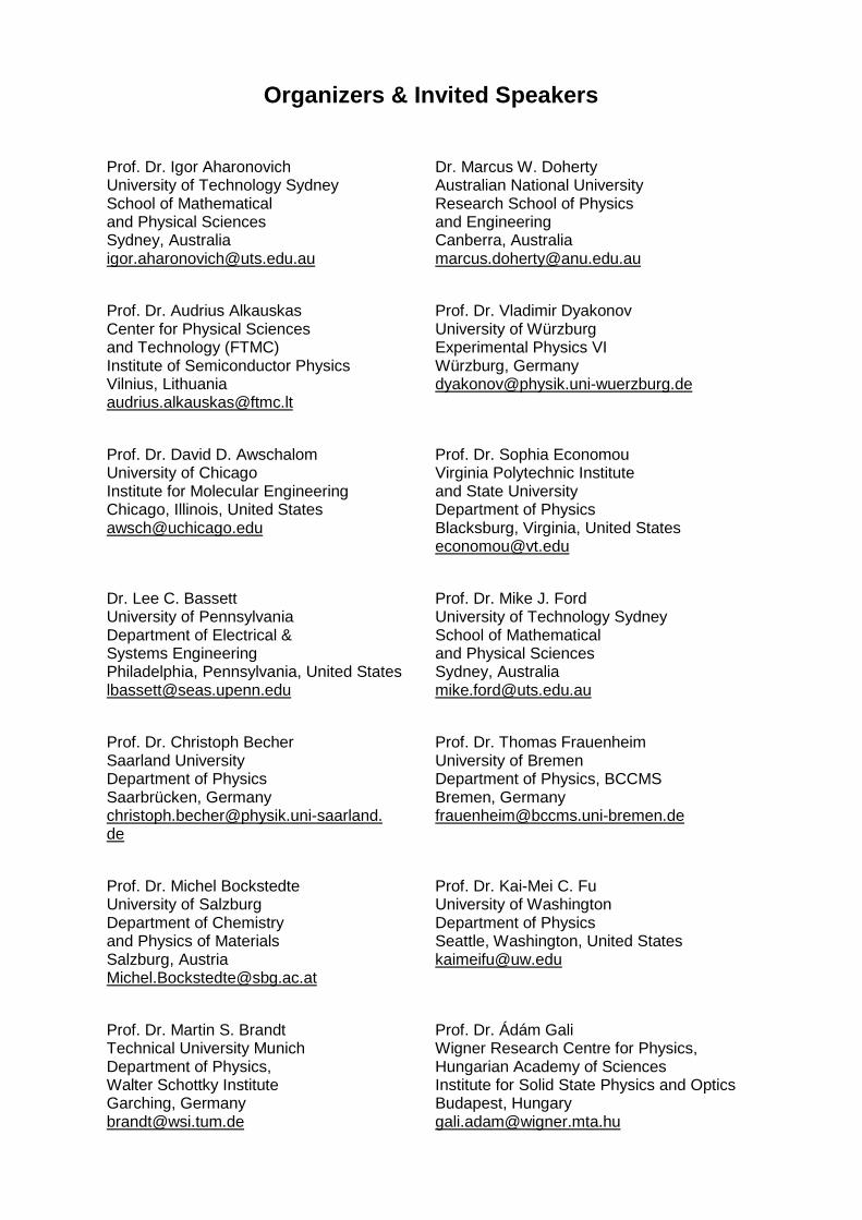
Organizers & Invited Speakers
Prof. Dr. Igor Aharonovich University of Technology Sydney School of Mathematical and Physical Sciences Sydney, Australia [email protected]
Prof. Dr. Audrius Alkauskas Center for Physical Sciences and Technology (FTMC) Institute of Semiconductor Physics Vilnius, Lithuania [email protected]
Prof. Dr. David D. Awschalom University of Chicago Institute for Molecular Engineering Chicago, Illinois, United States [email protected]
Dr. Lee C. Bassett University of Pennsylvania Department of Electrical & Systems Engineering Philadelphia, Pennsylvania, United States [email protected]
Prof. Dr. Christoph Becher Saarland University Department of Physics Saarbrücken, Germany [email protected]. de
Prof. Dr. Michel Bockstedte University of Salzburg Department of Chemistry and Physics of Materials Salzburg, Austria [email protected]
Prof. Dr. Martin S. Brandt Technical University Munich Department of Physics, Walter Schottky Institute Garching, Germany [email protected]
Dr. Marcus W. Doherty Australian National University Research School of Physics and Engineering Canberra, Australia [email protected]
Prof. Dr. Vladimir Dyakonov University of Würzburg Experimental Physics VI Würzburg, Germany [email protected]
Prof. Dr. Sophia Economou Virginia Polytechnic Institute and State University Department of Physics Blacksburg, Virginia, United States [email protected]
Prof. Dr. Mike J. Ford University of Technology Sydney School of Mathematical and Physical Sciences Sydney, Australia [email protected]
Prof. Dr. Thomas Frauenheim University of Bremen Department of Physics, BCCMS Bremen, Germany [email protected]
Prof. Dr. Kai-Mei C. Fu University of Washington Department of Physics Seattle, Washington, United States [email protected]
Prof. Dr. Ádám Gali Wigner Research Centre for Physics, Hungarian Academy of Sciences Institute for Solid State Physics and Optics Budapest, Hungary [email protected]
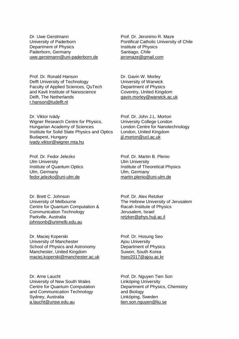
Dr. Uwe Gerstmann University of Paderborn Department of Physics Paderborn, Germany [email protected]
Prof. Dr. Ronald Hanson Delft University of Technology Faculty of Applied Sciences, QuTech and Kavli Institute of Nanoscience Delft, The Netherlands [email protected]
Dr. Viktor Ivády Wigner Research Centre for Physics, Hungarian Academy of Sciences Institute for Solid State Physics and Optics Budapest, Hungary [email protected]
Prof. Dr. Fedor Jelezko Ulm University Institute of Quantum Optics Ulm, Germany [email protected]
Dr. Brett C. Johnson University of Melbourne Centre for Quantum Computation & Communication Technology Parkville, Australia [email protected]
Dr. Maciej Koperski University of Manchester School of Physics and Astronomy Manchester, United Kingdom [email protected]
Dr. Arne Laucht University of New South Wales Centre for Quantum Computation and Communication Technology Sydney, Australia [email protected]
Prof. Dr. Jeronimo R. Maze Pontifical Catholic University of Chile Institute of Physics Santiago, Chile [email protected]
Dr. Gavin W. Morley University of Warwick Department of Physics Coventry, United Kingdom [email protected]
Prof. Dr. John J.L. Morton University College London London Centre for Nanotechnology London, United Kingdom [email protected]
Prof. Dr. Martin B. Plenio Ulm University Institute of Theoretical Physics Ulm, Germany [email protected]
Prof. Dr. Alex Retzker The Hebrew University of Jerusalem Racah Institute of Physics Jerusalem, Israel [email protected]
Prof. Dr. Hosung Seo Ajou University Department of Physics Suwon, South Korea [email protected]
Prof. Dr. Nguyen Tien Son Linköping University Department of Physics, Chemistry and Biology Linköping, Sweden [email protected]

Prof. Dr. Joerg Wrachtrup University of Stuttgart 3rd Institute of Physics Stuttgart, Germany [email protected]
Prof. Dr. Shengbai Zhang Rensselaer Polytechnic Institute Department of Physics, Applied Physics and Astronomy Troy, New York, United States [email protected]
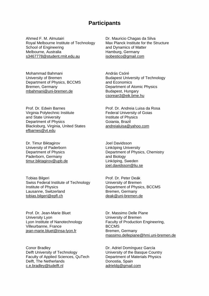
Participants
Ahmed F. M. Almutairi Royal Melbourne Institute of Technology School of Engineering Melbourne, Australia [email protected]
Mohammad Bahmani University of Bremen Department of Physics, BCCMS Bremen, Germany [email protected]
Prof. Dr. Edwin Barnes Virginia Polytechnic Institute and State University Department of Physics Blacksburg, Virginia, United States [email protected]
Dr. Timur Biktagirov University of Paderborn Department of Physics Paderborn, Germany [email protected]
Tobias Bilgeri Swiss Federal Institute of Technology Institute of Physics Lausanne, Switzerland [email protected]
Prof. Dr. Jean-Marie Bluet University Lyon Lyon Institute of Nanotechnology Villeurbanne, France [email protected]
Conor Bradley Delft University of Technology Faculty of Applied Sciences, QuTech Delft, The Netherlands [email protected]
Dr. Mauricio Chagas da Silva Max Planck Institute for the Structure and Dynamics of Matter Hamburg, Germany [email protected]
András Csóré Budapest University of Technology and Economics Department of Atomic Physics Budapest, Hungary [email protected]
Prof. Dr. Andreia Luisa da Rosa Federal University of Goias Institute of Physics Goiania, Brazil [email protected]
Joel Davidsson Linköping University Department of Physics, Chemistry and Biology Linköping, Sweden [email protected]
Prof. Dr. Peter Deák University of Bremen Department of Physics, BCCMS Bremen, Germany [email protected]
Dr. Massimo Delle Piane University of Bremen Faculty of Production Engineering, BCCMS Bremen, Germany [email protected]
Dr. Adriel Domínguez García University of the Basque Country Department of Materials Physics Donostia, Spain [email protected]
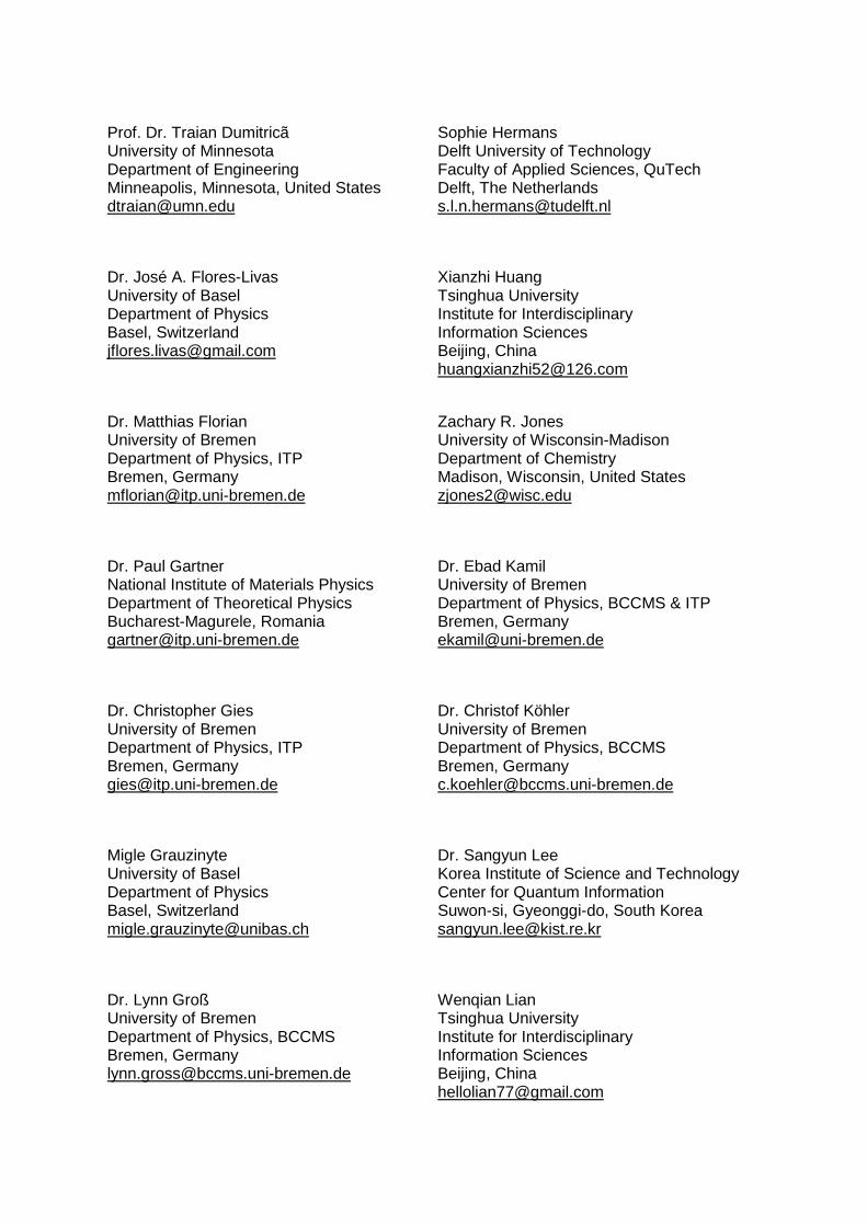
Prof. Dr. Traian Dumitricã University of Minnesota Department of Engineering Minneapolis, Minnesota, United States [email protected]
Dr. José A. Flores-Livas University of Basel Department of Physics Basel, Switzerland [email protected]
Dr. Matthias Florian University of Bremen Department of Physics, ITP Bremen, Germany [email protected]
Dr. Paul Gartner National Institute of Materials Physics Department of Theoretical Physics Bucharest-Magurele, Romania [email protected]
Dr. Christopher Gies University of Bremen Department of Physics, ITP Bremen, Germany [email protected]
Migle Grauzinyte University of Basel Department of Physics Basel, Switzerland [email protected]
Dr. Lynn Groß University of Bremen Department of Physics, BCCMS Bremen, Germany [email protected]
Sophie Hermans Delft University of Technology Faculty of Applied Sciences, QuTech Delft, The Netherlands [email protected]
Xianzhi Huang Tsinghua University Institute for Interdisciplinary Information Sciences Beijing, China [email protected]
Zachary R. Jones University of Wisconsin-Madison Department of Chemistry Madison, Wisconsin, United States [email protected]
Dr. Ebad Kamil University of Bremen Department of Physics, BCCMS & ITP Bremen, Germany [email protected]
Dr. Christof Köhler University of Bremen Department of Physics, BCCMS Bremen, Germany [email protected]
Dr. Sangyun Lee Korea Institute of Science and Technology Center for Quantum Information Suwon-si, Gyeonggi-do, South Korea [email protected]
Wenqian Lian Tsinghua University Institute for Interdisciplinary Information Sciences Beijing, China [email protected]
Dr. Zidu Liu Tsinghua University Institute for Interdisciplinary Information Sciences Beijing, China [email protected]
Dr. Michael Lorke University of Bremen Department of Physics, ITP & BCCMS Bremen, Germany [email protected]
Yanan Lu University of Chinese Academy of Sciences Institute of Physical Sciences Beijing, China [email protected]
Prof. Dr. Sanghamitra Neogi University of Colorado Boulder College of Engineering & Applied Science, Ann and H.J. Smead Aerospace Engineering Boulder, Colorado, United States [email protected]
Xiaolong Ouyang Tsinghua University Institute for Interdisciplinary Information Sciences Beijing, China [email protected]
Walter Pfäffle University of Hamburg Department of Physical Chemistry Hamburg, Germany [email protected]
Dr. Thomas Plisson Nuclear Physics Laboratory at CEA DAM Ile-de-France Department of Physics Arpajon, France [email protected]
Matteo Pompili Delft University of Technology Faculty of Applied Sciences, QuTech Delft, The Netherlands [email protected]
Dr. Joe A. D. Randall Delft University of Technology Faculty of Applied Sciences, QuTech Delft, The Netherlands [email protected]
Dr. Walid Redjem University of Montpellier Department of Physics Montpellier, France [email protected]
Mariya Romanova École Polytechnique Laboratory of Irradiated Solids Palaiseau, France [email protected]
Maximilian T. Ruf Delft University of Technology Faculty of Applied Sciences, QuTech Delft, The Netherlands [email protected]
Dr. habil. Dmitry A. Ryndyk University of Bremen Department of Physics, BCCMS Bremen, Germany [email protected]
Vladyslav O. Shkolnykov University of Konstanz Department of Physics Konstanz, Germany [email protected]
Dr. Abdallah Slablab Saarland University Department of Physics Saarbrücken, Germany [email protected]
Dr. Alexander Steinhoff University of Bremen Department of Physics, ITP Bremen, Germany [email protected]
Benedikt Tratzmiller Ulm University Institute of Theoretical Physics Ulm, Germany [email protected]
Péter Udvarhelyi Wigner Research Centre for Physics, Hungarian Academy of Sciences Institute for Solid State Physics and Optics Budapest, Hungary [email protected]
Min Wang Tsinghua University Department of Physics Beijing, China [email protected]
Prof. Dr. Tim O. Wehling University of Bremen Department of Physics, BCCMS &ITP Bremen, Germany [email protected]
David Wise University College London London Centre for Nanotechnology London, United Kingdom [email protected]
Yefei Yu Tsinghua University Institute for Interdisciplinary Information Sciences Beijing, China [email protected]
Huili Zhang Tsinghua University Institute for Interdisciplinary Information Sciences Beijing, China [email protected]
Wengang Zhang Tsinghua University Institute for Interdisciplinary Information Sciences Beijing, China [email protected]
Feihao Zhang Tsinghua University Department of Physics Beijing, China [email protected]