
CDT-PV Module 4 Mathematical Methods and … · CDT-PV Module 4: Mathematical Methods and...
52
CDT-PV Module 4 Mathematical Methods and Nanotechnology University of Southampton Feb 1 st -12 th 2016
Transcript of CDT-PV Module 4 Mathematical Methods and … · CDT-PV Module 4: Mathematical Methods and...

CDT-PV Module 4
Mathematical Methods and Nanotechnology
University of Southampton
Feb 1st -12th 2016

CDT-PV Module 4: Mathematical Methods and Nanotechnology.
Southampton Feb 1st -12th 2016
2
Course Timetable Monday 1st Feb Tuesday 2nd Feb Wednesday 3rd Feb Thursday 4th Feb Friday 5th Feb
09:00-10:00 Numerical methods Ian Hawkes B46/4121
10:00-11:00 CTM Lecture 1 Giles Richardson
B44/3031
Lab rotation 1 (Meet in B53 foyer, then
divide into groups for Lab A, B & C)
Lab rotation 2 (Meet in B53 foyer, then
divide into groups for Lab A, B & C)
11:00-12:00
12:00-13:00
13:00-14:00 Arrival lunch
14:00-15:00 Welcome, introduction, lab tours
safety briefing B02/1039 LT K
Numerical methods Ian Hawkes B44/3031
CTM Lecture 2 Giles Richardson B67/2017 T Rm 6
Team challenge prep Team challenge prep
15:00-16:00
16:00-17:00
17:00-18:30 CTM Lecture 3 Giles Richardson
B54/8031 8C
Monday 8th Feb Tuesday 9th Feb Wednesday 10th Feb Thursday 11th Feb Friday 12th Feb
09:00-10:00 Quiz B54/5025 5B
10:00-11:00 Lab rotation 3 (Meet in B53 foyer, then
divide into groups for Lab A, B & C)
CTM Lecture 5 Giles Richardson
B46/4121
Numerical methods Ian Hawkes
B67/2017 T Rm 6
Team challenge prep Team challenge prep
11:00-12:00
12:00-13:00 Restaurant Lunch
13:00-14:00
14:00-15:00 CTM Lecture 4 Giles Richardson B67/2013 T Rm 8
Numerical methods Ian Hawkes B54/7037 7B
Computer Lab: TCAD modelling for PV
Tasmiat Rahman Avenue B65/2143
Computer Lab: TCAD modelling for PV
Tasmiat Rahman Avenue B65/2143
Team Challenge Talks B54/7035 7B 15:00-16:00
16:00-17:00 Depart
17:00-18:30 CTM Lecture 6 Giles Richardson
B54/8031 8C

CDT-PV Module 4: Mathematical Methods and Nanotechnology.
Southampton Feb 1st -12th 2016
3
Locations on Highfield Campus
CDT-PV Module 4: Mathematical Methods and Nanotechnology.
Southampton Feb 1st -12th 2016
4
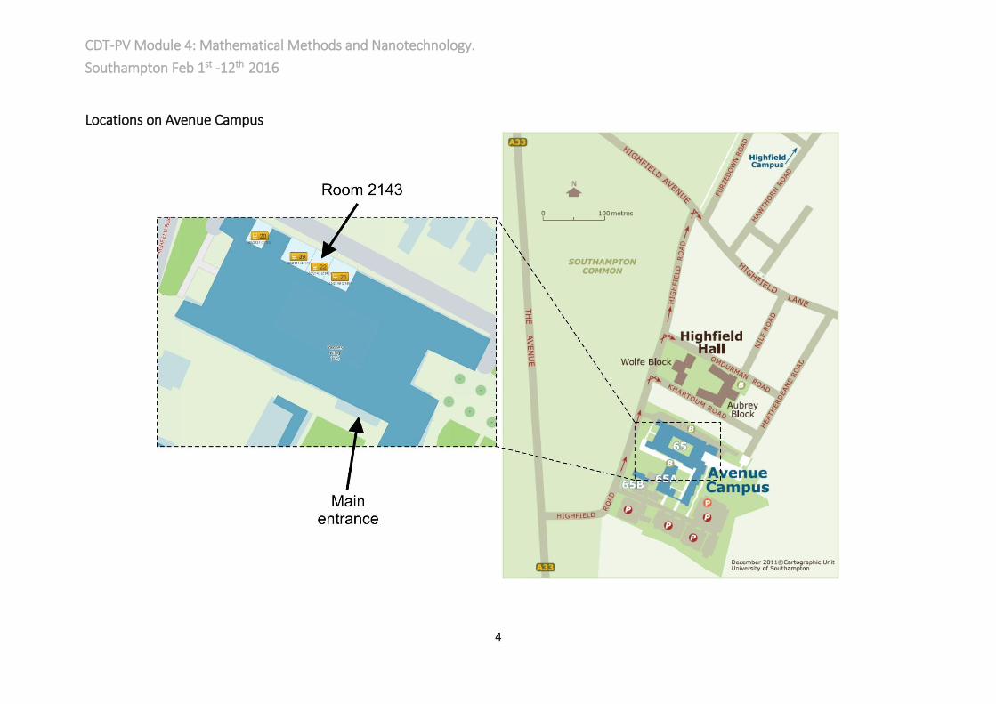
Locations on Avenue Campus

CDT-PV Module 4: Mathematical Methods and Nanotechnology.
Southampton Feb 1st -12th 2016
5
Lecture courses
Charge Transport Models Dr Giles Richardson
This is a 14 hour lecture course given in six sessions spread throughout the two weeks. The following topics will be covered:
• Hopping models and Monte Carlo Methods • Continuum models (drift diffusion) • Shockley equivalent circuits
Lecture notes for this course can be found at:
http://www.cdt-pv.org/media/resources/pv_notes_16.pdf
and are also included in the appendix of this booklet.
Numerical Methods Dr Ian Hawkes
This course will run over four sessions and will introduce you to the practical application of a relatively
wide spectrum of numerical techniques that can be implemented in Python.
Often in mathematics, it is possible to prove the existence of a solution to a given problem, but it is
not possible to "find it". For example, there are general theorems to prove the existence and
uniqueness of an initial value problem for an ordinary differential equation. However, it is in general
impossible to find an analytical expression for the solution. In cases like these numerical methods can
provide an answer, albeit limited: for example, there are numerical procedures (called algorithms)
that, given an initial value problem, will compute its solution.
This module is designed to cover four key areas:
Quadratures (i.e. the evaluation of definite integrals)
Solving ordinary differential equations.
Root finding
Solving partial differential equations.
The course material can be found at:
https://github.com/IanHawke/Southampton-PV-NumericalMethods-2016

CDT-PV Module 4: Mathematical Methods and Nanotechnology.
Southampton Feb 1st -12th 2016
6
Computer Lab
TCAD Modelling for PV Devices Dr Tasmiat Rahman
Unit cell of IBC solar cell formed using SPROCESS tool
The semiconductor industry is a multi-billion pound commerce of which computer aided design plays
a crucial role. At the device engineering stage Technology Computer Aided Design (TCAD) is prevalent.
It helps engineers optimize process flows and the device characteristics prior to fabrication. TCAD can
predict the electrical, optical, thermal and mechanical properties under set operating conditions given
the data is properly calibrated. TCAD is purely physics based - using fundamental physical models such
as drift-diffusion and Poisson equations to simulate the behaviour of devices.
TCAD packages consist of several tools, however the common four are: a graphical user interface
(GUI), a process simulator, a device simulator and finally a plotting tool. Numerous TCAD packages
exist including Synopsys, Silvaco, Crosslight and Cogenda. The dominant package in the TCAD field is
Synopsys, which is employed by 19 of the 20 leading semiconductor manufacturers. It is also used
extensively in the research field of semiconductor devices, most notably transistors and photovoltaics.
As such, it is a useful tool to learn. The four key tools used are Sentaurus Workbench, SProcess, SDevice
and SVisual.
SProcess models the various fabrication steps involved in semiconductor processing such as material
deposition, diffusion and etching, using various meshing strategies to generate a mixed grid element
mesh. This is advantageous as 3D structures can be formed from material growth and etching rather
than explicit geometry definition. This allows a means of forming complex 3D structures through
lithography steps followed by impurity diffusion as a function of time and temperature - key
processing steps that are common to PV fabrication.
SDevice simulates the electrical behaviour in a semiconductor device that is represented as a mesh
grid file. For PV devices, the input grid file should contain the geometry of the structure, the doping
profile and optical generation profile. Differential equations describing the electric potential and
carrier distributions are applied to each element of the mesh, with boundary conditions (i.e.
potentials) provided at each electrode. The equations are then solved to find the potential and carrier

CDT-PV Module 4: Mathematical Methods and Nanotechnology.
Southampton Feb 1st -12th 2016
7
concentrations in each element. The software uses a numerical solver which iterates repeatedly until
a solution converges to a given accuracy.
The objective of this course is to model an interdigitated back contact solar cell and optimise cell
design parameters. The outcomes will be as follows:
Become familiar with the Sentaurus TCAD tools – workbench, SProcess, SDevice, SVisual
Workbench
o Set simulation tool flow and define variables for optimization
SProcess:
o Basic process implementation – diffusion, etching, deposition steps.
o Mask design for photolithography
o Mesh refinement
o Contact definition
SDevice
o Define plot data
o Define physical models
o Define current-voltage sweep
SVisual
o Plot doping profiles to extract junction depth and peak concentration
o Plot IV sweep and extract Jsc, Voc and Efficiency.

CDT-PV Module 4: Mathematical Methods and Nanotechnology.
Southampton Feb 1st -12th 2016
8
CDT-PV Module 4: Mathematical Methods and Nanotechnology.
Southampton Feb 1st -12th 2016
Lab Rotations
Lab rotation 1 (Thurs 4rd Feb)
Lab rotation 2 (Friday 5th Feb)
Lab rotation 3 (Monday 8th Feb)
Group 1 Lab A Quantum Efficiency and
Reflectance
Lab C Time-resolved
Spectroscopy for PV
Lab B Microscopy in the
Cleanroom
Group 2 Lab B Microscopy in the
Cleanroom
Lab A Quantum Efficiency and
Reflectance
Lab C Time-resolved
Spectroscopy for PV
Group 3 Lab C Time-resolved
Spectroscopy for PV
Lab B Microscopy in the
Cleanroom
Lab A Quantum Efficiency and
Reflectance

CDT-PV Module 4: Mathematical Methods and Nanotechnology.
Southampton Feb 1st -12th 2016
9
Lab A
Quantum Efficiency and Reflectance
A Bentham Instruments PVE300 quantum efficiency characterization system
In this lab you will operate a Bentham PVE300 quantum efficiency characterization system to
characterize two types of crystalline silicon solar cell and various silicon samples treated to reduce
top surface reflectance. The purpose of these exercises is to develop background knowledge in
photovoltaic technologies and the methods used to characterize them within a research
environment.
A photovoltaic device will be most sensitive to a particular region of the spectrum, which depends in
part on the material from which the device is made. Specific types of solar cells can therefore be
selected to suit applications. The external quantum efficiency (EQE) of a solar cell is used to describe
the number of carriers collected by the solar cell to the number of photons of a given energy incident
on the solar cell, and can determine in which spectral region a particular device is performing strongly
or poorly. If all photons of a certain wavelength are absorbed and the resulting minority carriers are
collected, then the quantum efficiency at that particular wavelength is unity.
The EQE provides preliminary information regarding which regions of the solar spectrum to which the
device under test is most sensitive. In order to compensate for optical effects such as surface reflection

CDT-PV Module 4: Mathematical Methods and Nanotechnology.
Southampton Feb 1st -12th 2016
10
and transmission through the device, the internal quantum efficiency must be sought. This is
calculated per wavelength measurement using the following formula:
𝐼𝑄𝐸(𝜆) = 𝐸𝑄𝐸(𝜆)
[1 − R(𝜆) − T(𝜆) ]⁄
Where:
EQE (𝜆) = External Quantum Efficiency
R(𝜆) = Spectral Reflectance
T(𝜆) = Device Transmittance
The Bentham PVE300 QE system you will be using consists of a dual source producing white light which
is coupled through a monochromator and onto a solar cell. The wavelength of light incident on the
cell is varied and the current produced by the cell is measured. A calibration procedure is performed
so that the incident power is known for each wavelength. From this, the spectral response (A/W) of
the cell under test is calculated and then converted to a quantum efficiency. The system also features
an integrating sphere for the measurement of specular and diffuse reflectance and transmittance.
These measurements on solar cells enable the determination of IQE. The reflectance measurement
method can also be used on other samples, for example in the development of surface textures to
reduce top surface reflectance.
Experiments You will be provided with sections cut from two types of commercial crystalline silicon solar cell,
both provided by Solar Capture Technologies Ltd:
1. Screen printed
2. Laser grooved buried contact (LGBC)
Part 1: Quantum Efficiency 1. Collect EQE spectra for the two types of solar cell provided.
2. Measure the reflectance of your devices
3. Use the results to calculate the IQE of your devices (transmittance can be assumed to be
zero as these devices feature an opaque back contact).
Questions to consider:
What limits the QE in the different parts of the spectral range?
Why isn’t there a sharp cut off in spectral response at the silicon band gap (Eg=1.12 eV)?
What do the QE spectra from the two types of cell tell you about their relative performance?
Part 2: Reflectance Use the integrating sphere in the PVE300 to collected reflectance spectra from the samples of thin
films on silicon supplied.
The samples are labelled 1-8 on the reverse. From the reflectance spectrum and general appearance
of each sample, try to match it with the descriptions in the table on the following page. You may want
to use the online calculator OPAL2 available at www.pvlighthouse.com.au.

CDT-PV Module 4: Mathematical Methods and Nanotechnology.
Southampton Feb 1st -12th 2016
11
Sample number Surface
Bare Si (no coating)
30 nm SiO2
107 nm SiO2
125 nm SiO2
52 nm SiNx
84 nm SiNx
Random pyramids + SLAR
Regular inverted pyramids + SLAR
Questions to consider:
Which one is the best coating for a silicon solar cell?
How could this be further optimized?
Some notes on reflectance
The first step in achieving efficient conversion of light to electricity in a photovoltaic (PV) device is to
ensure that as much of the incident light as possible is transmitted through to the active layer and
absorbed there. This lab focuses on one type of optical loss that is detrimental to this efficient
capturing of light: Top surface reflection.
For normal incidence, the reflectance, R, from an interface between two materials with refractive
indices of n1 and n2 respectively is derived from the Fresnel equations and is given by:
𝑅 = |
𝑛2 − 𝑛1
𝑛2 + 𝑛1|
2
(1)
For absorbing materials, the reflectance is given by replacing the n terms in equation 1 by a complex
refractive index, ň, where
ň = 𝑛 − 𝑖𝑘 (2)
The imaginary component, k, describes absorption in the material and is often referred to as the
extinction coefficient. The reflectance is then given by:
𝑅 = |
ň2 − ň1
ň2 + ň1|
2
=(𝑛2 − 𝑛1)2 + (𝑘2 + 𝑘1)2
(𝑛2 + 𝑛1)2 + (𝑘2 + 𝑘1)2 (3)
Equations 1 and 3 show that the larger the difference between the refractive indices of the two
materials, the greater the reflectance at the interface between them. If we take crystalline silicon cells
as an example, the real part of the refractive index for silicon, n, ranges from 3.5 to 6.9 over
wavelengths in the range 300 to 1200 nm, which is high compared to materials such as glass and
ethylene vinyl acetate (EVA), that typically surround a solar cell in a module, for which n is

CDT-PV Module 4: Mathematical Methods and Nanotechnology.
Southampton Feb 1st -12th 2016
12
approximately 1.5 (see Figure 1). This leads to a normal incidence reflectance for an air-silicon
interface, which is important for laboratory cells, of between 31 and 61% and for an EVA-silicon
interface, found in encapsulated cells, of between 16 and 46% (see Figure 1).
Figure 1. Variation of real part of refractive index (n) for silicon and glass with wavelength and reflectance spectra for silicon-air and glass-air interfaces.
The manufacturers of crystalline silicon solar cells usually employ two methods to reduce top surface
reflection:
1. A thin film antireflection (AR) coating, consisting of a layer of material with refractive index
between that of the silicon and the surrounding medium. The thickness of the layer is specified
to produce destructive interference between light reflected at the different interfaces (Figure
2), therefore minimizing reflectance. Two or more layers can be used in the coating to produce
a broadband antireflective effect.
2. Texturing of the top surface reduces total reflection because light initially reflected from an
inclined region of a textured surface is often then incident on another inclined feature,
resulting in more light being coupled into the cell (Figure 3).

CDT-PV Module 4: Mathematical Methods and Nanotechnology.
Southampton Feb 1st -12th 2016
13
Figure 2. Schematics of operation of thin film antireflective coatings: (a) single layer (SLAR); (b) double layer (DLAR). The thicknesses and refractive indices of the coating materials are chosen to produce destructive
interference in the solar spectral range.
Figure 3. Diagrams of multiple reflection AR mechanism with two different texture types: (a) pyramids, (b)
bowl-like features.

CDT-PV Module 4: Mathematical Methods and Nanotechnology.
Southampton Feb 1st -12th 2016
14
Lab B
Microscopy in the Cleanroom
The Southampton Nanofabrication Centre is a state-of-the-art facility for microfabrication and high-
spec nanofabrication, as well as a wide range of characterization capabilities housed in the new
Mountbatten Complex at the University of Southampton. As one of the premier cleanrooms in Europe,
the Centre has a uniquely broad range of technologies, combining traditional and novel top down
fabrication with state-of-the-art bottom up fabrication. This allows us to develop and produce a wide
range of devices in diverse fields such as electronics, nanotechnology and bionanotechnology and
incorporate them into an equally comprehensive array of nano and microsystems for analysis and use.
The characterization capability is a similarly extensive catalogue of microscopes and test gear, from
nanometre resolution scanning microscopes to electrical, magnetic and RF analysis.
In this lab, you will get to put on a ‘bunny suit’ and go into the nanofabrication cleanroom to use some
of the state-of-the-art microscopy equipment housed there to image various samples related to silicon
photovoltaics research. The lab is divided into two sessions. During the first session, you will work with
an operator of the Zeiss Orion helium ion microscope (HIM) to capture images of the surfaces of
textured silicon samples and solar cells. In the second session you will learn how a gallium focused ion
beam system (Zeiss NVision40 FIB) can be used to mill a trench into the surface to prepare a cross-
section view of the top few microns of a sample. These techniques have broad applicability in solar
cell research, allowing us to develop a deeper understanding of the structure of devices we fabricate
and perhaps determine why a device may not be performing as it should. Included below is some more
background information on the HIM and FIB techniques.
Helium Ion Microscopy (HIM)
Diagram of the Carl Zeiss helium ion microscope showing some of its main features.

CDT-PV Module 4: Mathematical Methods and Nanotechnology.
Southampton Feb 1st -12th 2016
15
The Carl Zeiss Orion helium ion microscope (HIM) generates a focused beam of helium ions, with a
beam energy of 10-35 keV, and raster scans the beam across a sample, inducing the emission of
secondary electrons. An image is formed, pixel by pixel, from the emitted secondary electrons in the
same way as in a scanning electron microscope (SEM). The larger mass and therefore smaller de
Broglie wavelength of helium ions compared to electrons, combined with the extremely small and
bright source (courtesy of the atomically sharp tip at which helium atoms are ionised), and the small
interaction volume of the beam in the sample enables sub nanometer resolution to be achieved along
with a depth of field up to 5-10 times larger than in an SEM. The focused beam of ions can also be
used to modify samples on the nanometer scale by directly sputtering material in the same way as the
Ga focused ion beam. Insulating samples can be imaged without a conductive coating by using the
integrated electron flood gun to neutralize charge build up.
The ion gun in the Orion consists of a sharp metal needle-like emitter (the source) maintained at a
temperature of ~73K and in an ultra high vacuum (UHV, ~1e-9 Torr) when not operating. A high voltage
is applied to the source, creating a strong electric field between the source and an extractor plate,
concentrated at the tip of the source. During source formation the source is sharpened so that three
atoms (the ‘trimer’) form the very tip of the emitter. When helium is introduced into the gun region,
it drifts towards the tip under the influence of the field gradient. In narrow ionization zones, just above
the surfaces of the trimer atoms, the field is sufficiently concentrated to promote the quantum-
mechanical effect whereby an electron can escape from an atom by tunnelling through the energy
barrier that normally bonds it to the nucleus. If a gas atom loses an electron through this effect,
thereby becoming a positive ion, it is accelerated towards the negative extractor electrode (while its
freed electron is accelerated to the emitter and contributes to electron current flow in the high voltage
power supply circuit). The accelerated ion will gain sufficient linear velocity to pass through the
extractor electrode’s central orifice and it will proceed into the column optics.
Helium ion microscopy has several advantages over the more commonly available scanning electron
microscope (SEM). These include:
A higher resolution due to a smaller probe size and smaller interaction volume.
A larger depth of field due to a smaller beam convergence angle.
The ability to neutralise surface charging with an integrated electron flood gun, allowing
insulating samples to be imaged uncoated.

CDT-PV Module 4: Mathematical Methods and Nanotechnology.
Southampton Feb 1st -12th 2016
16
Gallium Focused Ion Beam (FIB)
The arrangement of FIB and SEM columns in the NVision40 FIB system.
The NVision 40 is a combined gallium focused ion beam (FIB) system and field emission gun scanning
electron microscope (FEGSEM) that can be used for microscopic examination and modification of
specimens.
The Gemini™ FEGSEM column features a Schottky field emission source that combines the advantages
of high brightness and high stability with a low energy spread to achieve edge resolutions down to 1.1
nm at 20 kV. The unique SEM column design also exhibits high performance at low beam energies so
that high resolution images (edge resolution is rated at 2.5 nm at 1 kV) that are rich in surface detail
can be obtained. There are two secondary electron detectors: An in-chamber Everhart-Thornley SE
detector and an in-lens annular scintillator detector. There is also a column-mounted backscattered
electron detector with a filtering grid adjustable from 0V to -1.5 kV for contrast adjustment. A
transmission detector (STEM) is also available for imaging thin specimens using the transmitted
electron signal.
The ion column features a Gallium liquid metal ion source (LMIS) that is capable of producing a focused
ion beam approaching at an angle of 54° to the vertical SEM beam. The probe current can be
automatically adjusted in the range 0.1 pA to 45 nA, with a beam energy of 30 keV to allow the user
to choose the right balance of probe size and sputtering yield for the particular milling/deposition
process. Lower beam energies are also available for fine scale polishing. Secondary electron imaging
with the ion beam is possible, with an edge resolution down to 4 nm.
An integrated gas injection system (GIS) is used for the deposition of metals and insulators. The
following precursors for tungsten, carbon and silicon dioxide. The process for cross-section
preparation involves four main processing steps:
1. Electron beam induced deposition of a protective layer of carbon or tungsten. 2. Ion beam induced deposition on the same area. 3. Automated or manual milling of a trench to expose a cross-section surface. 4. Ion beam polishing of cross-section surface.

CDT-PV Module 4: Mathematical Methods and Nanotechnology.
Southampton Feb 1st -12th 2016
17
Lab C
Time-resolved Spectroscopy for PV
Schematic of the setup to be use for this lab
In solid state physics, time-resolved spectroscopy is the study of the exciton dynamics by means of
spectroscopy study. Critical for PV applications, these methods can provide a valuable insight in the
formation and relaxation of excitons (coupled electron-hole pairs) within the p-n junction. Using ultra-
fast lasers, processes can routinely be resolved to a few femtoseconds. In this module, we’ll use a
tuneable femtosecond laser and time-correlated single photon spectroscopy to study the exciton
dynamics of a perovskite thin film and of a perovskite PV device. These measurements will be carried
on at room temperature (in air) and at ~10K (within a cryostat, in vacuum). This will allow us to gauge
the difference in exciton dynamics for different ambient conditions and draw some general
conclusions about the behaviour of excitons in p-n junctions.
The samples will be excited by a tuneable Ti:Sapphire laser (Coherent Chameleon) providing ~100fs
pulses for wavelengths between 680 and 1080nm. This source will be frequency doubled to obtain
excitation energies optimized with the perovskite absorption. Detection will be carried on using an
ultra-fast avalanche photo diode (APD) and time-correlated single photon spectroscopy (TCSPC). This
method is based on the precise time-registration of single photons emitted by the material studied (in
our case the perovskite film) for every excitation laser pulse. More details on the detection is available
at:
https://www.picoquant.com/images/uploads/page/files/7253/technote_tcspc.pdf,
which is a recommended read before the lab.

CDT-PV Module 4: Mathematical Methods and Nanotechnology.
Southampton Feb 1st -12th 2016
18
Team Challenge
Nanophotonics for PV
• Work in groups of 3
• Review the literature to investigate one type of nanophotonic technology being applied to
PV.
• Each team should prepare a presentation to give to the group on their assigned topic
• Aspects to address:
– Theory of operation
– Practical implementation
– Application to PV
– Scale-up potential
• Presentations to be given to the group on afternoon of the last Friday (12th Feb).
• 4 teams, 20 mins presentation, 5 mins questions
Presentation Topic
Group 1 Plasmonics
Group 2 Subwavelength Antireflective structures
Group 3 Diffractive elements/photonic crystals
Group 4 Quantum dots and resonant energy transfer
If a group would like to instead do a theoretical team challenge then this can also be arranged.

CDT-PV Module 4: Mathematical Methods and Nanotechnology.
Southampton Feb 1st -12th 2016
19
Appendix
Charge Transport Models Lecture Notes
Dr Giles Richardson

Models for charge transport in photovoltaic devices
Giles Richardson∗
January 25, 2016
1 Introduction
The aim of this short course is to give you some idea of the different approaches used to modelcharge transport in photovoltaic devices. The style of presentation reflects my background incontinuum mechanics (e.g. fluid mechanics, elasticity etc.) and so is rather different to thatencountered in a solid-state physics course. Nevertheless despite the difference in approachthe resulting models are the same and I hope that you will find it helpful to see things from adifferent perspective. It must be emphasised that the list of modelling approaches describedhere is far from comprehensive.
After the Introduction the material is divided into 4 further sections. In Section 2 webriefly review the equilibrium statistical mechanics of a semiconductor as this has somebearing on the non-equilibrium models that we consider in the subsequent 3 sections. InSection 3 we briefly discuss hopping models of charge transport and relate these to continuumdrift-diffusion model of the same process. In Section 4 we elaborate on the drift-diffusionmodel introduced in the previous section and apply this to the particular example of ann-p homojunction used as a solar cell. Furthermore we show that the current-voltage curvepredicted by modelling this device using a drift-diffusion model is accurately approximatedby a Shockley equivalent circuit. This leads us, in Section 5, to discuss Shockley equivalentcircuit models of solar cells and their use in inferring device physics from current-voltagedata.
2 Equilibrium electron and hole distributions in a semi-
conductor
We begin by briefly discussing the equilibrium distribution of charge carriers in a conventional(inorganic) semiconductor before going on to consider charge transport processes. The banddiagram of a semiconductor (i.e. the allowed electron energy levels) is characterised by anenergy gap between the valence band and conduction band in which there are no permissable
∗Mathematical Sciences, University of Southampton, Southampton SO17 1BJ.
1

electron states. This is illustrated in figure 1. Although it is usual to think of the valence andconduction bands being continuous in energy they are in fact comprised of a large numberof states, separated by very small energies. We therefore need to account for the density ofstates per unit energy in both conduction and valence bands. These are defined as follows
Number of states per unit volume in conductionband with energy between E and E + δE
≈ gc(E)δE, (1)
Number of states per unit volume in valenceband with energy between E and E + δE
≈ gv(E)δE, (2)
where δE is a small increment in energy. Now since electrons are fermions they obey aFermi-Dirac distribution at equilibrium. Thus the probability of a particular state, withenergy E, being occupied at temperature T is given by
P(E, T ) =1
1 + exp((E −Ef )/kBT )(3)
where Ef is a constant, termed the Fermi level, which is chosen so that the sum of the prob-abilities over all possible states gives the total number of electrons in the system. Assumingwe know the density of states we can now work out what the electron density in the valenceband nv and in the conduction bands nc using (1)-(3)
nc =
∫
∞
Ec
gc(E)
1 + exp((E − Ef ))/kBT )dE, (4)
nv =
∫ Ev
−∞
gv(E)
1 + exp((E − Ef)/kBT )dE. (5)
Note that the conduction band levels all lie above Ec while the valence band levels all liebelow Ev.
The Boltzmann approximation. In a typical semiconductor, at room temperature, thevalence band is very nearly full (i.e. almost all the states are occupied) while the conductionband levels are almost all empty (i.e. almost all the states are unoccupied). This is aconsequence of the energy gap Eg = Ec−Ev being large with respect to kBT (i.e. Eg ≫ kBT )and there being almost the right number of electrons to exactly fill the valence states. Thelatter is equivalent to the following conditions on the Fermi level
Ec − Ef
kBT≫ 1 and
Ef − Ev
kBT≫ 1. (6)
It follows that the integrand in (5) is almost gv(E) and this suggests that, rather thancounting the number of electrons in the valence band, we should count the number of empty
2

Valence Band
Vacuum Level
Conduction Band
0
Ec
Ev
EgEnergy Gap
Fermi LevelEf
Electron
Ea
Energy E
Figure 1: The allowed electron energy levels in a semiconductor (at zero electric potential).Here Eea is the ionisation potential and Eg the gap energy.
states. These empty states are, by convention, called holes and their density p is given by
p =
∫ Ev
−∞
gv(E)dE −
∫ Ev
−∞
gv(E)
1 + exp((E − Ef)/kBT )dE
=
∫ Ev
−∞
gv(E) exp((E − Ef)/kBT )
1 + exp((E −Ef )/kBT )dE
=
∫ Ev
−∞
gv(E)
1 + exp((Ef −E)/kBT )dE.
Since the exponential exp((Ef − E)/kBT ) is very large where the condition (6) is satisfiedwe can accurately approximate the expression for p by
p ∼
∫ Ev
−∞
gv(E) exp(−(Ef − E)/kBT )dE.
On making the subsitition E = Ev − V we obtain the expression
p ∼ exp
(
−Ef − Ev
kBT
)∫
∞
0
gv(Ev − V) exp
(
−V
kBT
)
dV. (7)
In a similar fashion we may approximate nc (the number density of electrons in the conduc-tion band), since from (6) exp((E−Ef )/kBT ) is very large. On dropping the subscript fromnc we find
n ∼
∫
∞
Ec
gc(E) exp(−(E − Ef ))/kBT )dE,
3

Then, on making the subsitition E = Ec + U , we obtain the expression
n ∼ exp
(
−Ec − Ef
kBT
)∫
∞
0
gc(Ec + U) exp
(
−U
kBT
)
dU . (8)
It is more usual to express these approximations for p and n in the form
p = Nv(T ) exp
(
−Ef − Ev
kBT
)
and n = Nc(T ) exp
(
−Ec − Ef
kBT
)
(9)
where
Nc(T ) =
∫
∞
0
gc(Ec + U) exp
(
−U
kBT
)
dU (10)
Nv(T ) =
∫
∞
0
gv(Ev − V) exp
(
−V
kBT
)
dV, (11)
where Nc and Nv are termed the effective conduction band and valence band densities ofstates, respectively. If, as is usual, the density of states in the vicinity of the conductionband and valence band are approximately parabolic, i.e. gc(Ec + U) ∼ ΥcU2 for U > 0 andgv(Ev −V) ∼ ΥvV2 for V > 0 for some constants Υc and Υv, we can evaluate these integralsexplicitly.
The intrinsic carrier density. A consequence of the Boltzmann approximation is thatproduct np is independent of the Fermi level, that is
np = Nc(T )Nv(T ) exp
(
−Eg
kBT
)
where Eg = Ec −Ev,
and Eg is termed the energy gap. It is perhaps more usual to write this relation in terms ofthe intrinsic carrier density ni defined by
np = n2i where ni = (Nc(T )Nv(T ))
1/2 exp
(
−Eg
2kBT
)
. (12)
The reason for doing this is that in an intrinsic (un-doped) semiconductor we have (atequilibrium)
n = p = ni.
Doping. Impurities in the semiconducting crystal can lead to dramatic changes in itselectrical properties. Foreign atoms in its crystal lattice may preferentially donate electronsto the conduction band (n-type doping) or grab them from the valence band (p-type doping)leading to an imbalance between the number of holes and electrons. In the case of n-typedoping this leads to a stationary net positive charge (the impurity atom loses one of itselectrons) while in the case of p-type doping this leads to a stationary net negative charge
4

(the impurity atom gains an electron). If these impurities occur in sufficient quantities theymay significantly increase the number of charge carriers above the intrinsic carrier density.This is a consequence of the net charge in the material having to remain close to zero (chargeneutrality). Thus if Nd denotes the density of donor impurities (fixed positive charges) whileNa denotes the density of acceptor impurities (fixed negative charges) the condition of chargeneutrality implies
q(p− n+Nd −Na) = 0. (13)
Hence if there are very few acceptor impurities and a large number of donor impurities withNd ≫ ni we expect (from (12)-(13)) that
n ≈ Nd p ≈n2i
Nd
Such a material is termed n-doped because it has very many more conduction electrons thanholes. Alternatively if there are very few donor impurities and a large number of acceptorimpurities with Na ≫ ni we expect (from (12)-(13)) that
p ≈ Na n ≈n2i
Na
Such a material is termed p-doped because it has very many more holes than conductionelectrons.
Doping can be used to enhance the conductivity of a semiconductor because a dopedmaterical typically has many more charge carriers than an undoped (or intrinsic) material. Itcan also be used as a mechanism to separate holes from electrons by p-doping a semiconductorin one region and n-doping it in another. This sets up a potential difference between thetwo regions that acts to drive holes into the p-doped region and electrons into the n-dopedregion and can thus be used to separate solar generated charge carrier pairs in a photovoltaicdevice.
3 Probabilistic and Drift-Diffusion models of charge
transport
We begin by considering models for a particle hopping on a lattice of energy wells and showthat in a certain limit the probability of finding the particle in a given well at a particuartime can be approximated by a diffusion equation. We generalise to a particle hopping ona lattice with an externally applied potential and show that its probability density satisfiesan drift diffusion equation. This analysis then applied to the motion of charge carriers in asemiconductor. We finish by applying the drift diffusion model of charge carrier transportin a semiconductor to a photovoltaic device formed from a p-n junction and show that itscurrent voltage curve is identical to that given by a simple equivalent circuit model of a solarcell.
5

i + 1i− 1 i
(a) (b)
U(x)
∆E(x)∆E
Figure 2: The energy landscape of the particle for (a) a lattice with no applied potential and(b) a lattice with applied potential U(x).
3.1 Rate equations for a particle hopping on a lattice
We start by considering a particle in one dimensional periodic energy landscape as depictedin figure 2(a). This is characterised by energy wells separated by intervening energy peaks.The particle sitting in one of these wells will, from time to time, have sufficient thermalenergy to traverse the energy maximum dividing this well from one of its neighbours. Therate at which this “hopping” process occurs is given by the Arrhenius equation
Pi→i+1 = Probability particle moves fromwell i to i+ 1 per unit time
= K exp
(
−∆E
kBT
)
Pi→i−1 = Probability particle moves fromwell i to i− 1 per unit time
= K exp
(
−∆E
kBT
)
where kB is Boltzmann’s constant; T is absolute temperature; ∆E is the energy differencebetween two neighbouring wells; and K a phenomenological rate constant.
The Dynamic Monte-Carlo method. We could at this stage simulate the motionof the particle simply by getting a computer to throw dice in order to decide what itdoes. The simplest way to do this is to pick a small time step ∆t with the property that
∆tK exp(
− ∆EkBT
)
≪ 1 (this means that in any given time step the chance of the particle
moving is small). Then to pick a random number R evenly distributed between 0 and 1 andimplement the procedure
If 0 ≤ R < ∆tK exp
(
−∆E
kBT
)
then i(t+∆t) = i(t)− 1,
If ∆tK exp
(
−∆E
kBT
)
≤ R < 2∆tK exp
(
−∆E
kBT
)
then i(t+∆t) = i(t) + 1,
If 2∆tK exp
(
−∆E
kBT
)
≤ R ≤ 1 then i(t+∆t) = i(t).
6

This is an extremely easy procedure to implement but it is numerically inefficient becausefor most of the time steps nothing happens and the particle remains where it is (to put itanother way it takes very little of your time to program but you may have to wait a longtime for the results if you are investigating a more complex problem than this).
The Gillespie Algorithm. It is, as remarked on above, computationally wasteful to takevery small timesteps in which nothing happens. An alternative, more efficient procedure, isto calculate the randomly distributed time T between the last event and the next one andthen to calculate what the next event is based on the relative probabilities of the possibleevents. Thus in the case of our previous example of a particle hopping on a one-dimensionallattice the next event is either that the particle hops right (with probablity per unit timePi→i+1) or that it hops left (with probablity per unit time Pi→i−1). So the
Probability of an eventoccuring in theinfinitessimal intervalT < t < T + δt
= Ptotδt where Ptot = Pi→i−1 + Pi→i+1. (14)
Given that the last event occurred at t = 0 the probability of the next event occurring inthe infinitessimal time interval T < t < T + δT is
Probability next eventoccurs inT < t < T + δt
=
Probability no eventsoccurs in interval0 < t < T
×
Probability an eventoccurs in intervalT < t < T + δt
, (15)
In order to evaluate this expression we need to calculate the probability that no events occurin 0 < t < T (we have already calculated the probability that an even occurs in T < t < T+δtin (14)). In order to do this we subdivide the interval 0 < t < T into a large number, N ,of very small intervals of size ∆t such that N∆t = T . An approximate expression for thisquantity is then given by
Prob. no eventsin interval0 < t < T
≈
Prob. no eventsin interval0 < t < ∆t
×
Prob. no eventsin interval∆t < t < 2∆t
× · · ·
· · · ×
Prob. no eventsin interval0 < t < N∆t
= (1− Ptot∆t)× (1−Ptot∆t)× · · · × (1− Ptot∆t),
= (1− Ptot∆t)N .
7

Taking the (natural) logarithm of this expression we find that
loge
Prob. no eventsin interval0 < t < N∆t
≈ N loge(1−Ptot∆t)
≈ −NPtot∆t since Ptot∆t ≪ 1
= −PtotT.
It follows that
Prob. no eventsin interval0 < t < N∆t
= exp(−PtotT ).
Substituting this result, together with (14), back into (15) we obtain the desired result
Probability next eventoccurs inT < t < T + δt
= Ptotδt exp(−PtotT ). (16)
How then should we use the result (16) to randomly select the time T at which thenext even occurs? Recall that it is easy to get a computer to pick a (uniformly distributed)random number R with value between 0 and 1. Furthermore the probability that the nextevent occurs in the interval 0 < t < T is a random variable that is distributed between 0and 1 (i.e. it is 0 when T = 0 and 1 when T = ∞). Indeed by integrating the expression(16) we find that
Probability next eventoccurs in range0 < t < T
=
∫ T
0
Ptot exp(−Ptott)dt (17)
= [− exp(−Ptott)]T0 (18)
= 1− exp(−PtotT ). (19)
In order to calculate the time T to the next event we therefore identify 1−exp(−PtotT ) withthe uniformly distributed variable R, with range 0 < R < 1, by writing
1− exp(−PtotT ) = R
from which we calculate T as
T = −1
Ptotloge(1− R). (20)
8

Once we have calculated the time T to the next event (using the uniformly distributedvariable R with range 0 < R < 1) we need to work out which of the two possible events (theparticle moves left or the particle moves right) occurs at this time. This is easy to do sincethe relative probabilities of these two events are
Relative probabilityparticle moves righti → i+ 1
=Pi→i+1
Ptot,
Relative probabilityparticle moves lefti → i− 1
=Pi→i−1
Ptot.
and the relative probabilites clearly add to 1. We therefore calculate which of the twopossibilities occurs (in the next event) by getting the computer to pick a second (uniformlydistributed) random number r, with value between 0 and 1, and
moving the particle moves to the right (i.e. i → i+ 1) if 0 < r <Pi→i+1
Ptot,
moving the particle moves to the left (i.e. i → i− 1) ifPi→i+1
Ptot< r < 1.
(21)
The Algorithm. To recap the Gillespie Algorithm for a particle hopping on a one-dimensional lattice consists of the steps
1. Use the computer to pick a (uniformly distributed) random number R with valuebetween 0 and 1.
2. Calculate the time T to the next event from the value of this random number with theformula
T = −1
Ptotloge(1− R).
3. Use the computer to pick a second (uniformly distributed) random number r withvalue between 0 and 1.
4. Determine which of the two events occur from the value of r based on the criterion
particle moves to the right (i.e. i → i+ 1) if 0 < r <Pi→i+1
Ptot
,
particle moves to the left (i.e. i → i− 1) ifPi→i+1
Ptot< r < 1.
(22)
5. Repeat.
Generalisation to more complicated systems. With a bit of common sense this algo-rtihm can be generalised to more complicated random systems where there are more thantwo possible events. For example the motion of a particle on a square lattice; here there are4 possible events (i) particle moves left, (ii) particle moves right, (iii) particle moves up, (iv)
9

particle moves down. Or for example N particles moving on a square lattice; here there are4N possible events corresponding to each particle moving in 1 of 4 directions. Or if we areinterested in carrying out a Monte-Carlo simulation of a solar cell we need to account forthe motion of a large number of holes and electrons on a lattice together with generationevents (creation of a hole and electron) and recombination events (destruction of a hole andelectron).
3.2 A probabilistic approach to particle hopping.
Rather than trying to directly simulate the motion of the particle it is often sufficient totrack the probability of the particle being at any particular lattice point as a function oftime. With this in mind we define
Pi(t) =Probability particle isin well i at time t
and attempt to write down a series of coupled ordinary differential equations (ODEs) in timefor the probabilities Pi(t) by considering the evolution of the system over an infinitesimaltime interval δt. Suppose that we know what the probability of finding the particle is atany of the lattice points at time t (that is we know all the Pi(t) for all values i) then theprobability that the particle is in the i’th well at time t + δt is given approximately by
Pi(t+ δt) ≈ Pi(t)×
(
Probability particle remainsin well i over interval δt
)
+Pi+1(t)×
(
Probability particle jumps fromwell i+ 1 to well i in interval δt
)
+Pi−1(t)×
(
Probability particle jumps fromwell i− 1 to well i in interval δt
)
. (23)
It follows that
Pi(t+ δt) ≈ Pi(t)
(
1− 2δtK exp
(
−∆E
kBT
))
+Pi+1(t)δtK exp
(
−∆E
kBT
)
+ Pi−1(t)δtK exp
(
−∆E
kBT
)
=⇒Pi(t+ δt)− Pi(t)
δt= K exp
(
−∆E
kBT
)
(Pi+1(t)− 2Pi(t) + Pi−1(t)) .
Taking the limit δt → 0
dPi
dt= K exp
(
−∆E
kBT
)
(Pi+1(t)− 2Pi(t) + Pi−1(t)) . (24)
10

3.3 Derivation of a diffusion equation for particle hopping.
In practise we might be thinking of applying this approach to a problem in which there area very large number of lattice sites: for example to an electron hopping along a line of atomsin a crystal. In such scenarios it is not sensible to track of the probability on all latticesites. Furthermore, since the probability at neighbouring lattice sites is likely to be verysimilar, we can seek to replace the probabilities Pi(t) on the lattice sites by a continuumrepresentation of the probability p(x, t), where we suppose x to be a spatial representationof the site’s position. Thus if the lattice sites are evenly spaced a distance δx apart we canwrite x = iδx. It is tempting to identify p(x, t) directly with Pi(t) by writing p(iδx, t) = Pi(t)but rather than do this we instead choose to define p(x, t) as a probability density by writing
p(iδx, t) =Pi(t)
δx
[Aside: You might be worried about the dimensions here because probability densities usuallyhave dimensions of L−3 and p(x, t) seems to have dimensions of L−1. However we note thatif we were considering a three-dimensional problem we would have defined p(x, y, z, t) by
p(iδx, jδx, kδx, t) =Pijk(t)
δx3(25)
which has the right dimensions and so if we are thinking of this as being a one-dimensionalrepresentation of a 3-d problem the units of Pi(t) really should be L−2 for the obviousreasons.]
Having defined p(x, t) by (25) and substituted this into (24) we retrieve
∂p
∂t(x, t) =
[
Kδx2 exp
(
−∆E
kBT
)]
p(x+ δx, t)− 2p(x, t) + p(x− δx, t)
δx2
If we now Taylor expand p(x+δx, t) and p(x−δx, t) about x (assuming that δx is sufficientlysmall to allow us to do so) we find that, to a leading order approximation, that p(x, t) satisfiesa diffusion equation
∂p
∂t= D
∂2p
∂x2, (26)
where
D =
[
Kδx2 exp
(
−∆E
kBT
)]
. (27)
11

Interpretation in terms of particle number density (concentration). Thus far wehave assumed only a single particle hopping on a lattice but in reality we are much moreoften concerned with a large number of particles on a lattice (e.g. free electrons in an organicsemiconductor or excitons). This does not present a problem provided that the particles donot interact with each other via, for example, Coulomb forces or exclusion effects. We willleave the treatment of interaction via Coulomb forces until §3.4 and note here that exclusioneffects only become significant when the number of particles is comparable to the number oflattice sites so that there is competition between particles for available lattice sites. Hence,provided the particles do not interact via a force and their number is much smaller thanthat of the lattice sites, we can treat them as effectively independent. This means each ofthe N particles has a probability density p(n)(x, t) (for n = 1, 2, · · · , N) which is, to a goodapproximation, independent of that for all the other particles. It follows that the particlenumber density c(x, t) defined by
c(x, t) =
N∑
n=1
p(n)(x, t),
obeys the same equation that the probability distribution for each particle obeys (i.e. (26)).Thus
∂c
∂t= D
∂2c
∂x2, (28)
3.4 Description of a particle hopping on a lattice in an appliedpotential
Semiconductors contain relatively large numbers of mobile charged particles (free electronsand holes) which, since they are charged, interact with each other via the Coulomb potential.In order to treat this type of scenario we consider a single particle moving in a potentialcomprised of a quasi-periodic part (as previously) and a smooth part U(x) (the appliedpotential); this is illustrated in figure 2(b). In order to make the analysis more general weallow the energy barrier between the wells (in the absence of the applied potential) ∆E tovary smoothly with x; the implicit assumption being that ∆E varies by a small amountbetween neighbouring peaks but can vary significantly over many peaks. We denote theenergy barrier on passing from well i to well i+1 by ∆Ei→i+1 and that on passing from welli to well i − 1 by ∆Ei→i−1. In the presence of the applied potential U(x) the appropriateexpressions for these quantities are
∆Ei→i+1 = U
(
x+δx
2
)
− U(x) + ∆E
(
x+δx
2
)
, (29)
∆Ei→i−1 = U
(
x−δx
2
)
− U(x) + ∆E
(
x−δx
2
)
, (30)
12

where, as before x = iδx. In a similar fashion
∆Ei+1→i = U
(
x+δx
2
)
− U(x+ δx) + ∆E
(
x+δx
2
)
, (31)
∆Ei−1→i = U
(
x−δx
2
)
− U(x− δx) + ∆E
(
x−δx
2
)
. (32)
Once again we consider a small time interval δt and formulate a set of coupled difference equa-tions for Pi(t+ δt) (the probability of the particle being in well i at time t+ δt) as describedin equation (23). The rate at which the particle jumps from one well to a neighbouring wellare (as before) determined by the energy barrier that it has to surmount, through Arrhenius’Law. We can thus translate (23) into the following difference equation
Pi(t+ δt) ≈ Pi(t)
(
1− δtK
(
exp
(
−∆Ei→i+1
kBT
)
+ exp
(
−∆Ei→i−1
kBT
)))
+Pi+1(t)δtK exp
(
−∆Ei+1→i
kBT
)
+ Pi−1(t)δtK exp
(
−∆Ei−1→i
kBT
)
.
On rearranging this equation and taking the limit as δt → 0 we obtain a set of coupledODEs (exactly as before), namely
dPi
dt= K
[
Pi+1(t) exp
(
−∆Ei+1→i
kBT
)
+ Pi−1(t) exp
(
−∆Ei−1→i
kBT
)
−Pi(t)
(
exp
(
−∆Ei→i+1
kBT
)
+ exp
(
−∆Ei→i−1
kBT
))]
. (33)
In order to obtain a partial differential equation for the probability density p(x, t) (as definedin (25)) we proceed as before and expand in powers of δx (having first substituted for theenergy barriers from (29)-(32)). As this is a rather lengthy procedure we won’t give thedetails here but we note that that the calculation is of a similar nature to that used to derive(26) and that the resulting PDE is
∂p
∂t=
∂
∂x
(
D(x)
(
∂p
∂x+
p
kBT
∂U
∂x
))
, (34)
where
D(x) =
[
Kδx2 exp
(
−∆E(x)
kBT
)]
.
Using arguments analogous to those presented at the end of §3.3 we can show that the sameequation is satisfied by the particle number density c(x, t), i.e.
∂c
∂t=
∂
∂x
(
D(x)
(
∂c
∂x+
c
kBT
∂U
∂x
))
, (35)
in a system in which the number of particles is much smaller than the number of lattice sites.
13

Generalisation to higher dimensions. It is straightforward (but slightly messy) to showthat the one dimensional drift diffusion equation generalises to three-dimensions to give, asmight be expected,
∂c
∂t= ∇ ·
(
D(x)
(
∇c+c
kBT∇U
))
, (36)
3.5 Other processes giving rise to advection-diffusion models
The above description of particle motion in a periodic energy landscape could easily beadapted to free electrons in the LUMO (lowest unoccupied molecular orbital) of an organicsemiconductor (or equally to a hole in the HOMO of an organic semiconductor). However itdoes not apply to conduction electrons in an inorganic semiconductor which occupy a gen-uine conduction band and are therefore free to move largely unhindered through the crystallattice. Nevertheless the same drift-diffusion equation, derived above in (34), applies to themotion of electrons in a conduction band and holes in a valence band except that here thediffusive character of the motion can be attributed to electron scattering in the crystal lat-tice. The derivation of the drift-diffusion equations in an inorganic semiconductor is outlinedin Nelson (chapter 3) [7].1 This derivation is considerably more involved than the one givenabove for hopping processes. It starts (I) from a quantum mechanical description of thewavefunction of an electron in the conduction band of a semiconducting lattice (using Blochwave functions), (II) assumes that electrons are in quasi thermal equilibrium at all pointsin space (i.e. scattering of electrons within the crystal is sufficiently fast that the electronsare distributed [across energy levels of the conduction band] according to a Boltzmann dis-tribution) and (III), having made this assumption, uses the Boltzmann Transport equationto calculate the electron current in terms of the electric field and the spatial distribution ofelectrons.
4 Drift diffuion models of charge transport in semicon-
ductors
Charge transport in a semiconductor is characterised by the motion of free electrons (in theconduction band [inorganic] or LUMO [organic]) and holes (in the valence band [inorganic]or HOMO [organic]). Both electrons and holes are charged and therefore interact via theCoulomb force. In order to keep track of these interactions it is usual to define an ‘averaged’electric potential φ which satisfies Poisson’s equation
∇ · (ε∇φ) = −ρ(x, t) (37)
where ε is the permittivity. The charge density ρ is typically approximated in terms ofp, n and Cfix which are the hole, free electron and the fixed charge densities (or in other
1See also Feynman Volume III [1] Chapters 13-14.
14

words Cfix = Nd − Na is the net doping density), respectively. The relation given by thisapproximation is
ρ(x, t) = q(p(x, t)− n(x, t) + Cfix) (38)
where q is the charge on a proton. In making this approximation we have smeared out theeffects of the individual point charges by replacing the delta-functions in the charge densitywith a smooth function q(p(x, t)−n(x, t)+Cfix). Where opposite charges do not tend to pairup this is a sensible approach to adopt. Indeed it works well for semiconductors however,there are systems, such as electrolytes, where this approximation is not particularly goodand alternative approaches have to be adopted.
Assuming that there is very little charge recombination or generation the resulting equa-tions for n, p and φ can be found by combining (37) with (38), writing c = p and U = qφ in(36) and writing c = n and U = −qφ in (36) to obtain the set of coupled PDEs
∂p
∂t= ∇ ·
(
Dp
(
∇p+q
kBTp∇φ
))
, (39)
∂n
∂t= ∇ ·
(
Dn
(
∇n−q
kBTn∇φ
))
, (40)
∇ · (ε∇φ) = q(n− p− Cfix). (41)
Here Dp and Dn are the diffusivity of holes and mobile electrons, respectively.
Remarks. It is notable that there are 3 PDEs for the 3 variables p, n and φ and we thereforeseem to have the right number of equations for unknowns. There are however a number ofthings missing from the physics. Firstly we have entirely neglected charge generation andrecombination which are key ingredients if we want to model a solar cell. Secondly we haveimplicitly assumed that we are considering only a single materialn when in fact we may wantto investigate devices with junctions between a number of semiconducting materials.
4.1 Currents, fluxes and carrier concentration
In order to aid the physical interpretation of their solutions it is helpful to recast the drift-diffusion equations for free electrons and holes in terms of alternative variables (e.g. quasi-Fermi levels). We begin re-expressing (36) (or alternatively (39)-(40)) in terms of conserva-tion laws for the carrier concentrations. On writing c = p in (36) and subsequently writingc = n in (36) and re-arranging the resulting equations we find
∂p
∂t+∇ · (pvp) = 0 where vp = −
Dp
kBT∇
(
kBT ln
(
p
c∗p
)
+ Up
)
, (42)
∂n
∂t+∇ · (nvn) = 0 where vn = −
Dn
kBT∇
(
kBT ln
(
n
c∗n
)
+ Un
)
. (43)
15

Here it is not immediately clear what the reference concentrations c∗p and c∗n should be, andit does not matter provided we only consider a single homogenous material in which theseconcentrations are constant so that their gradients are zero. In fact it turns out (for soundstatistical mechanical reasons) that we should identify c∗p and c∗n with the effective densitiesof states in the valence and conduction bands, respectively (see (11)) so that
c∗p = Nv and c∗n = Nc
We may identify (42a) and (43a) as conservation equations for p and n respectively in whichvp and vn represent the average velocities of holes and electrons respectively. Equations (42b)and (43b) for the average velocities can then be re-expressed in terms of thermodynamicquantities as
vp = −Dp
kBT∇µp where µp = kBT ln
(
p
Nv
)
+ Up, (44)
vn = −Dn
kBT∇µn where µn = kBT ln
(
n
Nc
)
+ Un. (45)
Here µp and µn are the electrochemical potentials of holes and free electrons, respectively.The hole current density jp (i.e. that portion of the current carried by holes) and the
electron current density jn are related to the average carrrier velocities by jp = qpvp andjn = −qpvn from which it follows that
jp = −qDp
kBTp∇µp and jn =
qDn
kBTn∇µn.
In the solid state physics literature these quantities are more usually expressed in terms ofcarrier mobilities and quasi Fermi levels in the form
jp = Mpp∇EFpand jn = Mnn∇EFn
. (46)
Here the electron and hole mobilities (Mn and Mp, respectively) and the electron and holequasi Fermi levels (EFn
and EFp, respectively) are defined by
Mn =qDn
kBT, Mp =
qDp
kBT, EFn
= µn, EFp= −µp. (47)
Electron and hole potentials and quasi-Fermi levels. We now need to specify theelectron and hole potentials (Un and Up respectively) more precisely. We begin by consideringthe mobile electrons. These electrons lie close to the lower edge of the conduction band andso in the absence of an electric field (i.e. zero electric potential) their energy is −Eea, whereEea is the electron affinity; i.e. the energy required to remove an electron from the conductionband edge to the vacuum level (see figure 1). The electrostatic part of the potential is −qφ.Adding these two contributions together gives
Un(x) = −Eea(x)− qφ(x). (48)
16

The holes lie close to the upper edge of the valence band and in order to calculate theirpotential we calculate the potential of an electron lying there and note that the potential ofa hole (i.e. a lack of an electron) is just minus that of the electron it replaces. It follows that
Up(x) = (Eea(x) + Eg(x)) + qφ(x), (49)
where Eg is the energy gap between the valence and conduction band2 (see figure 1). It isalso common to see the electron and hole potentials written in terms of the electron energies(including the effect of the electric potential) at the band edges
Un(x) = Ec(x) and Up(x) = −Ev(x). (50)
Here Ec and Ev are the energies at the conduction and valence band edges, respectively. Itnow becomes apparent why EFn
and EFpare termed quasi-Fermi levels because if we take
our definitions of the quasi-Fermi levels (47c-d) and substitute for the chemical potentials µp
and µn from (44b) and (45b) and rewrite the resulting expression in terms of p and n (using(50)) we obtain
p = Nv exp
(
−EFp
− Ev
kBT
)
and n = Nc exp
(
−Ec − EFn
kBT
)
. (51)
These look almost identical to (9) the formulae for the electron and hole denisities at equilib-rium except that the Fermi level in the equation of for n has been replaced by the quasi-Fermilevel EFn
and the Fermi level in the equation of for p has been replaced by the quasi-Fermilevel EFp
. However the formulae (51) dont really help us a lot because we cannot use themto determine the carrier concentrations n and p and it is much better to think of the quasi-Fermi levels as being determined by the carrier concentrations rather than the other wayround. With this in mind we use the definitions of the quasi-Fermi levels in (47c-d), (45b)and (44b) together with those of the electron and hole potentials to write
EFn= kBT ln
(
n
Nc
)
−Eea − qφ, EFp= −kBT ln
(
p
Nv
)
−Eea − Eg − qφ. (52)
4.2 Carrier generation and recombination
Thinking back to our treatment of a semiconductor at equilibrium it becomes apparent thatwe have forgotten something. Our equations for the conservation of electrons (42)-(43) allowonly for transport of electrons within a band but no interchange of electrons between the twobands (conduction and valence). Yet when we discussed the equilibrium problem we assumedthat there was thermal equilibrium between the electrons in the two bands and so we clearlyneed to allow jumping of electrons between bands, even if this might be a relatively smalleffect with respect to other processes. If we don’t do this we cannot expect the solution of our
2Here −(Eg + Eea) is the energy of an electron at the upper edge of the valence band at zero electricpotential.
17

model to eventually settle down to an equilibrium. How should we model this? Equations(42)-(43) are conservation equations for holes and free electrons respectively. Now movingan electron from the valence band to the conduction band results in the creation of a hole(in the valence band) and a free electron (in the conduction band). Similarly a free electroncan only jump down from the conduction band into the valence band if there is hole for itto fill and so this process therefore results in the annihilation of a free electron and a hole.In other words motion of electrons between bands results in the creation (or annihilation)of equal number of holes and free electrons. It follows that the only sensible way to alter(42)-(43) is by adding the same term to the right-hand side of both these equations so that
∂p
∂t+∇ · (pvp) = Gtherm,
∂n
∂t+∇ · (nvn) = Gtherm. (53)
Here it is to be understood that Gtherm is the volumetric rate of generation of holes and freeelectrons and can be either positive (if there is positive net rate of electrons jumping fromconduction to valence band) or negative (if there is positive net rate of electrons jumpingfrom valence to conduction band). Furthermore we require that, if the semiconductor isisolated and there are no spatial gradients (so that vp = vn = 0), the solution to (53) settlesto the thermodynamic equilibrium given in (12) for long times (i.e. np → n2
i as t → +∞). Ifwe think first about the recombination of free electrons (in the conduction band) with holes(in the valence band) we might reasonably expect that, since both species are rare, the ratelimiting step is getting the free electron close enough to the hole so that they can annihilate.The rate at which these two species come within a critical reaction radius per unit volume isclearly proportional to the product of their concentrations np. Putting these facts togetherwe end up with a simple (and correct) model for the thermal generation rate
Gtherm = γ(n2i − np). (54)
for some material dependent rate constant γ.
Solar generation. Central to the use of semiconductors in solar cell is their ability toabsorb light and turn the absorbed energy into charge free-electron hole pairs. Clearlysuch pairs can only be generated directly if the absorbed photon has more energy than theband gap, which is one of the reasons that the choice of material with the right band gapis so important. If the band gap is large not many photons are turned into free-electronhole pairs but the free-electron hole pairs that are generated have a large potential energy(corresponding to a high open circuit voltage Voc and a small short-circuit current Jsc). If onthe other hand the band gap is small most photons will generate free-electron hole pairs butthese will have low potential energy (corresponding to a high Jsc and low Voc). In inorganicsemiconductors (where the band gap is usually large) the generation of charge pairs typicallyoccurs directly throughout the bulk of the semiconductor. In organic materials, however,charge pair generation typically occurs in a two stage process. Photons are absorbed inthe bulk of the semiconductor to produced an exciton (an excited electron) which can bethought of as a coulombically bound electron hole pair. This exciton can diffuse around but
18

has a relatively short lifetime before it releases its energy as heat. Such excitonic materialscan only be used in photovoltaics if they form an interface with another material at whichit is favourable for excitons to dissociate into a free-electron in one material and a holein the other. As this is rather complicated we will stick to the direct form of generation(which incidentally also seems to be that relevant for perovskites). At its crudest level weought be able to treat such carrier generation in a similar fashion to thermal generation byadding a term Gsol(x) to the right-hand side of (53). Of course the exact details of thesize of Gsol and its spatial variation are extremely important and as hinted to above dependon band gap, the radiation spectrum and how much radiation has been absorbed in otherparts of the cell before reaching the point x. However these are not the focus of this courseand so we will not go into these here, and typically will assume Gsol is a constant (whichcan only really be justified in a very thin cell which absorbs only a small fraction of theincident light). It is worth noting that the rate of solar generation (per sufficiently energeticphtoton) is intimately linked to the rate of bimolecular recombination γ. This is becausesolar generation and bimolecular recombination are essentially the same processes but inreverse. For more information on how these rates should be calculated see Chapter 4 [7].3
Recombination via trapped states. Thus far we have assumed that charge pairs onlyrecombine via bimolecular recombination, in which an electron from the conduction banddrops direcly into a hole in the valence band; this is represented by the second (negative) termon the right-hand side of (54) (i.e. −γnp). Bimolecular recombination is, as noted above,the reverse process to solar generation since the potential energy lost by the conduction bandelectron is emitted as a photon. Indeed bimolecular recombination is responsible for lightemission in an LED (light emitting diode), which is a device that turns electrical energyinto light energy. However other recombination mechanisms are possible and indeed turnout to be more significant that bimolecular recombination in photovoltaic devices. Thesealternative forms of recombination usually occur when an electron from the conduction bandbecomes trapped in an energy state lying in the forbidden energy. Such states are termedtrap states and are associated with imperfections in the semiconductor. The most commonmodel for recombination via trapped states is the Shockley-Reid-Hall (SRH) model thatstates that the rate of recombination Rtrap has the form
Rtrap =np− n2
i
τ1n+ τ2p+ τ3ni, (55)
where τ1, τ2 and τ3 are timescales associated with the trapping process. Other more exoticrecombination processes are discussed in [6, 9].
4.3 The full equations
We are now in a position to write down the full equations for a semiconductor, which maybe doped, and which absorbs light to generate charge carrier pairs. These are given by (46)
3Assuming that the recombination and generation rates are independent can lead to nonsensical predic-tions such as devices that produce more power than they absorb through solar radiation.
19

and the generalisation of (53) to include solar generation Gsol and recombination via trappedstates Rtrap
∂p
∂t+
1
q∇ · jp = γ(n2
i − np) +Gsol(x)−Rtrap where jp = Mpp∇EFp, (56)
∂n
∂t−
1
q∇ · jn = γ(n2
i − np) +Gsol(x)− Rtrap where jn = Mnn∇EFn, (57)
∇ · (ε∇φ) = q(n− p− Cfix), (58)
where the quasi-Fermi levels are (as in (52)) defined by
EFp= −kBT ln
(
p
Nv
)
− (Eea + Eg)− qφ, (59)
EFn= kBT ln
(
n
Nc
)
−Eea − qφ. (60)
4.3.1 Boundary conditions.
Boundary conditions on these equations need to be specified where the semiconductor formsa junction with a current collectors. The latter are usually metallic or have metallic proper-ties. In most devices it is usual to assume that the metallic contact and the semiconductorare in thermal equilibrium. Even this assumption still yields rather complicated boundaryconditions which typically result in a solution with a thin layer in which the potential changesrapidly. However in practice the contacts are usually chosen so that they do not unduly in-fluence the behaviour of the device and where this is the case a sensible set of boundaryconditions, at the interface between a doped semiconductor and a metallic contact, consistsof imposing continuity of the potential at the contacts, requiring that the minority carriercurrent flux across the boundary is zero and ensuring that the carrier charge density is equalto the doping charge density: that is
Jmin · n|∂Ω = 0, φ|∂Ω = V, n− p|∂Ω = Cfix. (61)
Here V is the potential of the contact, n is the unit normal to the boundary and Jmin is thecurrent flux of the minority carrier.
4.4 A simple one-dimensional inorganic solar cell: the n-p homo-junction
Here we will consider a solar cell formed from a planar inorganic semiconductor sandwichedbetween two contacts (see figure 3) at x = −L and x = L and look to calculate its currentvoltage curve. In order to separate solar generated charges the semiconductor is n-dopedin −L < x < 0 and p-doped in 0 < x < L. At equilibrium, as illustrated in figure 4, thisresults in band bending and a potential difference between the two sides of the cell that actsto drive the electrons and holes created by solar generation apart. In order to simplify the
20

Contact
x = −L
x = 0
x = L
p-type
n-type
Contact
Figure 3: The n-p junction.
problem consider a cell with a high degree of symmetry. In particuar assume that the dopingin the two halves of the cell is equal and opposite (such that Cfix = Ndop in −L < x < 0 andCfix = −Ndop in 0 < x < L) and that the mobilities of holes and electrons are equal. Weshall also assume (rather unrealistically) that recombination is entirely bimolecular (so thatRtrap ≡ 0). With these assumptions the governing equations (56)-(60) may be written as
∂jp∂x
= q(
γ(n2i − np) +Gsol
)
, jp = −qD
(
∂p
∂x+
p
VT
∂φ
∂x
)
, (62)
∂jn∂x
= −q(
γ(n2i − np) +Gsol
)
, jn = qD
(
∂n
∂x−
n
VT
∂φ
∂x
)
, (63)
∂2φ
∂x2=
q
ε(n− p−Ndop) in −L < x < 0
q
ε(n− p+Ndop) in 0 < x < L
. (64)
Here we have chosen to rewrite mobility M in terms of the diffusion coefficient via D =kBTM/q and have defined VT = kBT/q. The quantity VT , termed the thermal voltage, playsan important role in semiconductor physics and at room tempertature VT ≈ 25mV.
Boundary Conditions at the contacts. Here we use the boundary conditions of theform (61) at both contacts. On the left contact (x = −L) the minority carriers are holes whileon the right contact they are electrons. We choose to split voltage difference V between thetwo contacts into two parts, the built in voltage Vbi and the applied voltage Vap, by writingV = Vbi − Vap; the boundary conditions then become
jn|x=−L = 0, φ|x=−L =Vbi − Vap
2, n− p|x=−L = Ndop, (65)
jp|x=L = 0, φ|x=L =Vap − Vbi
2, p− n|x=−L = Ndop, (66)
21

(b)
EnergyEnergy
Evac
Ec
Ef
Ef
Evn-type p-type
(a)
e−
Evac
Ec
n-type p-type
Vbi
x = −L x = 0 x = L
p+Ev
Ef
Figure 4: (a) Energy levels in the isolated n-type and p-type materials. (b) Band bendingand the built voltage Vbi when two materials form an n-p junction.
4.4.1 Rescaling.
We now have the option of trying to solve this model computationally for physically realisticparameters. However this does not really allow us to develop much physical intuition aboutthe problem and it turns out that a much better way of proceding is to try and solve themodel asymptotically (i.e. approximately) making use of the fact that certain dimensionlessparameters (these are sometimes termed dimensionless groups) are either very small or verylarge in all practical devices. As an example of this let us consider the ratio of the ratioof the Debye length LD (i.e. the characteristic lengthscale defined by equation (64)) to thehalf-width of the cell. Here on assuming that the characteristic volatge of the problem is VT
and the characteristic carrier density is Ndop we find that
LD =
(
εVT
qNdop
)1/2
.
Given ε ∼ 4ε0 andNdop ∼ 1022−1025m−3 gives LD in the range 10−9−10−8m. Comparing thisto a typical half width of a cell, which might be 10−6−10−5m, implies that the dimensionlessparameter λ defined by
λ =LD
L=
1
L
(
εVT
qNdop
)1/2
(67)
is very small λ = O(10−4)−O(10−2), a fact that we shall make use of.In order to identify all the dimensionless parameters in the problem we rescale it in such
a way as to leave a dimensionless problem charactersied by a minimal set of dimensionlessparameters. This process is called non-dimensionalisation and, providing that we choose toscale our variables with sensible values, leads to considerable insight into the physics of theproblem.
22

Nondimensionalisation. We resacle the variables in the problem as follows:
φ = VT φ, n = Ndopn, p = Ndopp, Gsol = G1−sunG, jn = qLG1−sunjn,x = Lx, Vbi = VT Vbi, Vap = VT Vap jp = qLG1−sunjp.
where given the application we choose to scale the charge pair generation term with thegeneration that would be expected under illumination of one sun G1−sun. On substitutingthese rescalings into (62)-(66) we obtain the following system on dimensionless equationsand boundary conditions:
∂jp∂x
= Θ(N2i − np) + G, jp = −κ
(
∂p
∂x+ p
∂φ
∂x
)
, (68)
∂jn∂x
= −Θ(N2i − np)− G, jp = κ
(
∂n
∂x− n
∂φ
∂x
)
, (69)
∂2φ
∂x2=
1
λ2(n− p− 1) in −1 < x < 0
1
λ2(n− p+ 1) in 0 < x < 1
, (70)
jp|x=−1 = 0, φ|x=−1 =Vbi − Vap
2, n− p|x=−1 = 1, (71)
jn|x=1 = 0, φ|x=1 =Vap − Vbi
2, p− n|x=1 = 1, (72)
where the dimensionless parameters (or groups) in the problem are
Ni =ni
Ndop
, λ =1
L
(
εVT
qNdop
)1/2
, Θ =
(
γN2dop
G1−sun
)
, κ =
(
DNdop
G1−sunL2
)
. (73)
Dimensionless parameters and their size. We have already seen that λ = LD/L givesthe ratio of the Debye length to the half-width of the cell. The next parameter we consideris Ni which gives the ratio of the intrinsic carrier density to that of the doping density; theintrinsic carrier density in silicon (at room temperature) is roughly 1016m−3 and so takingNdop ∼ 1020 − 1022m−3 (as above) leads to an estimate of Ni = O(10−4)−O(10−8). Θ givesthe ratio of the square of the typical charge densities obtained by balancing solar generationwith bimolecular recombination to the square of the doping density. κ gives the ratio of thetypical current density produced by a potential difference across the cell of size O(VT ) tothe current density produced by charge generation at one sun. Thus if κ ≫ 1 this suggeststhe current produced by illumination of the solar cell at one sun can be transported awayby a very small potential diffference across the cell, or to put it another way that the ohmicresistance is negligible. It is nearly always the case that κ ≫ 1, indeed if it were not the cellwould be very inefficient.
23

Simplifying the problem using its symmetry. The problem is symmetric about x = 0as can be seen by making the substitution
x = −X, p = N , n = P , φ = −Φ, jn = Jp, jp = Jn,
in (68)-(72). If you do this you will see that you retrieve exactly the same problem but withthe variables replaced as follows:
x → X, n → N, p → P , φ → Φ, jn → Jn, jp → Jp,
(check this). It is thus apparent that the solution to (68)-(72) has the symmetry
p(−x) = n(x), n(−x) = p(x), φ(−x) = −φ(x), (74)
jp(−x) = jn(x), jn(−x) = jp(x). (75)
We need therefore only solve in 0 < x < 1 where we impose the boundary conditions
p|x=0 = n|x=0, φ|x=0 = 0, jp|x=0 = jn|x=0.
The problem we need to solve in 0 < x < 1 can thus be stated as
∂jp∂x
= Θ(N2i − np) + G, jp = −κ
(
∂p
∂x+ p
∂φ
∂x
)
, (76)
∂jn∂x
= −Θ(N2i − np)− G, jp = κ
(
∂n
∂x− n
∂φ
∂x
)
, (77)
∂2φ
∂x2=
1
λ2(n− p+ 1), (78)
p|x=0 = n|x=0, φ|x=0 = 0, jp|x=0 = jn|x=0, , (79)
p− n|x=1 = 1, φ|x=1 =Vap − Vbi
2, jn|x=1 = 0, (80)
and we can determine the solution in −1 < x < 0 from the symmetry conditions (75).
4.4.2 Asymptotic solution to the dimensionless model in the limit λ ≪ 1 andκ ≫ 1
We now seek to solve the problem approximately by making use of the fact that κ ≫ 1 andλ ≪ 1. We start by noting that since κ ≫ 1 the right-hand sides of (76) and (77) must bothbe very small, i.e. the following approximate equations must hold
∂p
∂x∼ −p
∂φ
∂x,
∂n
∂x∼ n
∂φ
∂x.
It is not hard to show that these have solution
p = A exp(−φ) and n = B exp(φ), (81)
24

for some arbitrary constants A and B. Apllying the conditions (79a-b) on x = 0 implies that
B = A
while application of the conditions (80a-b) on x = 1 implies that
A =1
exp(
Vbi−Vap
2
)
− exp(
− Vbi−Vap
2
) =1
2 sinh(
Vbi−Vap
2
) ,
so that (81) can now be rewritten
p =exp(−φ)
2 sinh(
Vbi−Vap
2
) , n =exp(φ)
2 sinh(
Vbi−Vap
2
) . (82)
Substituting for p and n in (78) we find the following Poisson-Boltzmann equation for φ:
∂2φ
∂x2=
1
λ2
sinh(φ)
sinh(
Vbi−Vap
2
) + 1
, (83)
with boundary conditions
φ|x=0 = 0 and φ|x=1 = −Vbi − Vap
2. (84)
The small λ limit. Now we know that λ ≪ 1. This means that the term in the bracketson the right-hand side of (83) must be very small, i.e.
sinh(φ)
sinh(
Vbi−Vap
2
) ∼ −1.
The only solution to this approximate equation is
φ ∼ −Vbi − Vap
2, (85)
which obviously satisfies the second of the boundary conditions (84) but not the first. Theproblem here is that we cannot expect to neglect the highest derivative in an ODE and stillsatisfy its boundary conditions so that our naive approximation (85) fails. Problems in whichwe are tempted to neglect the highest derivative, but get into trouble doing so, are calledsingular perturbation problems. And, as we shall see, their solutions often have boundarylayers in which the solution varies rapidly. Indeed, as we shall show, this is precisely whathappens here and in fact
φ ∼ −Vbi − Vap
2for λ ≪ x < 1. (86)
25

− Vbi−Vap
2
λ 1φ
Figure 5: Illustration of the solution of (83)-(84) for φ with λ ≪ 1.
That is the approximation only fails in a narrow region of size O(λ) around x = 0 (this isillustrated in figure 5). If the solution is indeed as we have postulated in figure 5 then weought to be able to investigate the rapid transition from φ = 0 at x = 0 to the approximatesolution (86) for x ≫ λ by rescaling x with λ by writing
x = λz
On making this substitution into (83) and (84) we get
∂2φ
∂z2=
sinh(φ)
sinh(
Vbi−Vap
2
) + 1
with φ|z=0 = 0, (87)
and if it is indeed to tend towards the approximate solution (86), for large z, we must imposethe far-field condition
φ → −Vbi − Vap
2as z → +∞. (88)
Provided you believe that there is a solution to (87) satisfying the far-field condition (88) itis now fairly easy to find a good approximation to the current voltage curve for the device.In fact it turns out that there is a relatively straightforward to show that such a solutionexists provided that Vbi − Vap > 0 by using a phase-plane analysis.
Excercise: Write w = φz and then write the ODE (83a) as two coupled first order au-tonomous ODEs of the form φz = w and and wz = f(φ). Sketch the phase-plane for thesecoupled ODEs and show that there is a trajectory linking φ = 0 to a critical point at w = 0,φ = −(Vbi − Vap)/2 when Vbi − Vap > 0 and hence argue that a solution to the problem(87)-(88) exists when Vbi − Vap > 0.
26

Calculating the current voltage curves (I). Now we know n and p nearly everywherein 0 < x < 1 except very close to x = 0. It follows that we can get a very good approximationto the amount of recombination occuring and hence work out a current voltage curve. Sinceφ ∼ (Vap − Vbi)/2 in almost all of 0 < x < 1 it follows from (82) that
n ∼exp
(
− Vbi−Vap
2
)
2 sinh(
Vbi−Vap
2
) , p ∼exp
(
Vbi−Vap
2
)
2 sinh(
Vbi−Vap
2
) , (89)
The built-in voltage Vbi. Lets look first at what happens when there is zero solar gener-ation G ≡ 0 and zero applied voltage Vap = 0 and the device is allowed to reach equilibriumso that jn = jp = 0. These assumptions combined with (76a) and (77a) imply that np = N2
i .On subsituting the values of n and p, as determined in (89) with Vap = 0, into this relationgives an equation for Vbi
sinh2
(
Vbi
2
)
=1
4N2i
.
This can be further simplified by noting that (in all practical applications) Ni the ratio ofthe intrinsic carrier density to the doping density is very small which implied that Vbi is largeand given (approximately) by
Vbi ∼ 2 ln
(
1
Ni
)
. (90)
Translating this back into dimensional variables (via (68)) this gives
Vbi = 2VT ln
(
Ndop
ni
)
, (91)
which is precisely the result we would get from looking at the band bending and lining upthe Fermi levels (which is reassuring).
Calculating the current voltage curves (II). We now look at the case where thegeneration term G (which is assumed constant) and the applied voltage Vap are both non-zero and attempt to calculate the total current density j = jn + jp as a function of theapplied voltage. The equations and boundary conditions for the current densities become,on substituting for n and p from (89) in (76a), (77a), (79b) and (80a),
∂jp∂x
= Θ
N2i −
1
4 sinh2(
Vbi−Vap
2
)
+ G, (92)
∂jn∂x
= −Θ
N2i −
1
4 sinh2(
Vbi−Vap
2
)
− G, (93)
jp|x=0 = jn|x=0, jn|x=1 = 0. (94)
27

Notably the terms on the right-hand side of (92) and (93) are constant so that they arestrightforward to integrate. In particular
[jp − jn]1x=0 = 2
G−Θ
1
4 sinh2(
Vbi−Vap
2
) −N2i
so that, since jp − jn|x=0 = 0 (from (79c)) and jn|x=1 = 0 (from (80c)), it follows that thedimensionless current density j = jn = jp is given by
j = jp|x=1 = 2
G−Θ
1
4 sinh2(
Vbi−Vap
2
) −N2i
.
Furthermore since Vbi − Vap is typically large (i.e. in dimensional terms many thermal volt-ages) we can approximate 4 sinh2
(
(Vbi − Vap)/2)
∼ exp(Vbi − Vap) so that, on substitutingfor Vbi from (90), we obtain
j ∼ 2(
G−N2i Θ(eVap − 1)
)
. (95)
Rewriting this in terms of the original dimensional variables, using (68) and (73), we find
j = 2qL
(
G− γn2i
(
exp
(
Vap
VT
)
− 1
))
. (96)
As we shall show in the §5 this corresponds precisely to the current voltage relation of acurrent source strenght 2qLG in parallel with an ideal diode (ideality factor 1) with reversesaturation current density 2qLγn2
i .
Excercise: Modify the above argument to calculate the current voltage curve where recombi-nation primarily occurs via traps and can be modelled by a Shockley-Reid-Hall recombinationterm as given in (55).
5 Shockley equivalent circuit models of photovoltaic
devices
Drift diffusion models of charge transport, although they are capable of accurately describingthe behaviour of photovoltaics, have the disadvantage of being complicated and hard to solve.Indeed numerical solutions of these models in the right parameter regimes are frequently verydifficult to obtain with any degree of accuracy. When comparing to experimental data itis often easier to make use of phenomenological equivalent circuit models. At their verysimplest these consist of a current source term (representing the current generated by solarradiation) in parallel with a diode (see figure 6(a)) which represents the effects of chargerecombination. Indeed, as we shall show, the current-voltage curve that we obtained fromour approximate analysis of a drift-diffusion model of an np-homojunction (96) is preciselyof this form.
28

(b)
V V
I I
Rp
Rs
IgIg
(a)
Figure 6: Shockley equivalent circuits for a solar cell. (a) simple circuit for an n-p diode (b)the generic Shockley equivalent circuit.
V
I
(a) (b)
I/Is
V/VT
Figure 7: (a) Illustration of the direction of the current flow I through, and voltage V across,a diode. (b) The current-voltage curve for a diode with ideality Nid = 1.
The current voltage curve of a diode. The current I through a diode is related to thevoltage across it V by the relation
I = Is
[
exp
(
V
NidVT
)
− 1
]
, (97)
where Is and Nid are termed the reverse saturation current and the ideality factor respec-tively. Since this relation is asymmetric the diode (as a device) has directionality and thisis illustrated in figure 7.
The simple Shockley equivalent circuit (figure 6a). We now use the diode current-voltage curve, defined in (97), in the simple equivalent circuit in figure 5a. Note that thediode figure 5a points in the opposite direction to that in figure 7. The current flowingthrough the diode, from left to right, is thus
Idiode = −Is
[
exp
(
V
NidVT
)
− 1
]
.
29

addiing this current to the current Ig from the current source gives the total current I flowingthrough the circuit
I = Ig − Is
[
exp
(
V
NidVT
)
− 1
]
. (98)
Note that this current-voltage curve has exactly the same form as the current-voltage curvewe predicted from the n-p homojunction in §4.4, i.e. (96), provided we identify
Ig = 2AqLG, Is = 2Aqγn2i , Nid = 1.
Here A is the area of the homojunction so that I = jA. One rather interesting consequenceof assuming that recombination is entirely bimolecular is the prediction that the idealityfactor Nid = 1. If instead we had assumed that the dominant form of recombination wereSRH recombination then we would have found that the ideality factor Nid = 2. Other formsof recombination give other ideality factors, for example Auger recombination (see [7]) givesan ideality factor of 3.
Other devices. Whilst our analysis of the n-p homojunction in §4.4 shows that it isappropriate to fit current voltage data for such a device to an equivalent circuit model itis not obvious that this approach is appropriate for other devices. Roughly speaking ifthe device has planar material and doping interfaces that run parallel to the contacts anequivalent ciruit description will provide a consistent approximation of its behaviour. In [2]an analysis of a planar organic bulk heterojunction is made which results in a current-voltagecurve that is well approximated by a Shockley equivalent circuit whilst in [3] a similar typeanalysis is conducted for a planar (tri-layer) perovskite cell. It should be emphasised thatcells with non-planar geometry cannot usually be modelled by a Shockley equivalent circuit(e.g. heterogeneous organic bulk heterojunctions).
The generic Shockley equivalent circuit (figure 6b). The generic Shockley equivalentcircuit contains a shunt resistance Rp in parallel with a diode and a current source. Thethree parallel elements are connected in series with a resistor Rs. By splitting the voltageinto two parts: V1 (the voltage drop acoss diode, shunt resistance and current source) andV2 the voltage drop across Rs, we obtain the following set of equations
V = V1 + V2,
Idiode = −Is
[
exp
(
V1
NidVT
)
− 1
]
Current through diode,
Ishunt = −V1
RpCurrent through shunt resistor,
I = Ig + Ishunt + Idiode Conservation of current (Kirchoff),
V2 = −IRs Current through series resistor.
30

Figure 8: Fitting an equivalent circuit model to current-voltage data from bilayer hetero-junction organic solar cells (see [8]). Filled symbols represent cells under illumination opensymbols cells in the dark. Notice the current has been plotted on a log scale.
It is straightfoward to combine these expressions to obtain a single implicit expression forthe current voltage curve
I = Ig − Is
[
exp
(
V + IRs
NidVT
)
− 1
]
−V + IRs
Rp
. (99)
What is the physical basis for series and shunt resistances. We have already seenthat charge recombination in an n-p homojunction leads to the diode like behaviour of thisdevice. So what processes give rise to the shunt resistance and the series resistance usedto model real photovoltaic devices? The series resistance Rs can arise as a result of theresistance of the contacts or because of the resistance of the semiconductor itself. The lattereffect can be fairly readily incorporated into the analysis that we conducted in §4.4. Theshunt resistance is in some sense more interesting because it usually arises from shortingbetween the contacts. This might arise because there are regions where one of the dopedlayers are absent and the other spans the entire width of the cell or because dendrites havegrown directly from one contact to the other. In either case a low value of Rp can beattributed to some fault in the manufacture of the cell. This is therefore clearly somethingto look out for when fitting current voltage curves to an equivalent circuit.
Use of equivalent circuits models to fit to real data. Here we show a couple ofexamples of fits to real current-voltage data. In figure 8 we show fitted data taken fromPotscavage et al. [8] for current-voltage curves measured from three different designs ofbilayer heterojunction organic solar cells. In the cases of the data plotted with triangles andsquares the ideality factor Nid ≈ 2 corresponding to SRH recombination, while in the caseof data plotted with circles Nid ≈ 1.7 In figure 9 we show a comparison of an experimentalcurrent voltage curve obtained from a perovskite cell and the fit using a simple equivalent
31

0 0.2 0.4 0.6 0.8 1−200
−150
−100
−50
0
50
100
150
200
Voltage (V)
Cur
rent
den
sity
(A
/m2 )
(a)
0.4 0.6 0.8−200
−150
−100
10 15 20 25 30 35 40−2
−1
0
1
2
3
4
5
6
7
log(q∫x=b/2
x=−b/2G(s)ds+
J)
qV/kT
(b)
Figure 9: Fitting an equivalent circuit model to current-voltage data from a perovskite cell(prepared by Giles Eperon). From the data it is inferred that the ideality factor Nid ≈ 3.For more details see [3]. Note that the current has been defined in an opposite sense to thatin the text (to agree with the text the figure should be flipped about the V -axis).
circuit (taken from [3]). Here the ideality factor is Nid ≈ 3.Whilst this high ideality factormight be attributable to Auger recombination we believe it is more likely related to thehysteretic behaviour of perovskite cells.
References
[1] R.P. Feynman, R.B. Leighton & M. Sands, “Lectures on Physics (Volume III)”. AddisonWesley (2003).
[2] J. M. Foster, J. Kirkpatrick & G. Richardson, “Asymptotic and numerical prediction ofcurrent-voltage curves for an organic bilayer solar cell under varying illumination andcomparison to the Shockley equivalent circuit”. J. Appl. Phys., 114: 104501 (2013).
[3] Foster J.M., Snaith H.J., Leijtens T. & Richardson G., “A model for the operationof perovskite based hybrid solar cells: formulation, analysis and comparison to experi-ment”. SIAM J. Appl. Math. 74, 1935-1966 (2014).
[4] D. T. Gillespie, “Exact stochastic simulation of coupled chemical reactions”. J. Phys.Chem. 81, 2340-2361 (1977).
[5] Guarnera S., Abate A., Zhang W., Foster J.M., Richardson G., Petrozza A. & SnaithH.J. “Improving the long-term stability of perovskite solar cells with a porous Al2O3
overlayer”. J. Phys. Chem. Lett. 6, 432-437 (2015).
[6] T. Kirchartz, B. E. Pieters, J. Kirkpatrick, U. Rau & J. Nelson, “Recombination of tailstates in polythiopene: fullerene solar cells”. Phys. Rev. B., 83:115209 (2011).
[7] J. Nelson, “The physics of Solar cells”. Imperial College Press, (2003).
32

[8] W. J. Potscavage, S. Yoo & B. Kippelen, ‘Origin of the open-circuit voltage in amultillayer heterojunction organic solar cell’, Appl. Phys. Lett. 93, 193308 (2008).
[9] A. Schenk & U. Krumbein, “Coupled defect-level recombination: Theory and applica-tion to anomolous diode characteristics”. J. Appl. Phys., 78: 3185-3192 (1995).
[10] C. Schmeiser & A. Unterreiter, “The derivation of analytic device models by asymptoticmethods”. Semiconductors, Part II, IMA Vol. in Math. and its Appl. 59, Springer-Verlag(1993).
[11] S. M. Sze, K. Ng Kwok, “Physics of Semiconductor Devices”. 3rd edition, Wiley-Interscience NY, (2006).
[12] A. B. Walker, “Monte Carlo studies of electronic processes in dye-sensitized solar cells”,Topics in Current Chemistry (2013).
33