CDM Series PRO Series - WordPress.com · Detailed Service Manual. ... The information contained in...
178
CDM Series ™ PRO Series ™ Professional Series Two-Way Mobile Radios Detailed Service Manual
Transcript of CDM Series PRO Series - WordPress.com · Detailed Service Manual. ... The information contained in...

CDM Series™
PRO Series™
Professional Series
Two-Way Mobile Radios
Detailed Service Manual
Motorola
This document is in three parts. Download all three files and use the bookmarks on the left-hand side to navigate between the documents. Since the files have been collated, many of the cross-chapter references do not work.

Product Safety and RF Exposure Compliance
ATTENTION!This radio is restricted to occupational use only to satisfy FCC RF energy exposure requirements. Before using this product, read the RF energy awareness information and operating instructions in the Product Safety and RF Exposure booklet enclosed with your radio (Motorola Publication part number 6881095C99) to ensure compliance with RF energy exposure limits.For a list of Motorola-approved antennas, batteries, and other accessories, visit the following web site which lists approved accessories: http://www.motorola.com/cgiss/index.shtml.
ForewordThe information contained in this manual relates to all CDM Series and PRO Series models of Professional Series two-way mobile radios. This manual provides sufficient information to enable qualified service technicians to troubleshoot and repair a Professional Series two-way mobile radio to the component level.
Manual RevisionsChanges which occur after this manual is printed are described in FMRs (Florida Manual Revisions). These FMRs provide complete replacement pages for all added, changed, and deleted items, including pertinent parts list data, schematics, and board overlays. To obtain FMRs, please contact the Customer Care and Services Division (CCSD). (Refer to the Appendix in the back of this manual for contact information.)
Computer Software CopyrightsThe Motorola products described in this manual may include copyrighted Motorola computer programs stored in semiconductor memories or other media. Laws in the United States and other countries preserve for Motorola certain exclusive rights for copyrighted computer programs, including, but not limited to, the exclusive right to copy or reproduce in any form the copyrighted computer program. Accordingly, any copyrighted Motorola computer programs contained in the Motorola products described in this manual may not be copied, reproduced, modified, reverse-engineered, or distributed in any manner without the express written permission of Motorola. Furthermore, the purchase of Motorola products shall not be deemed to grant either directly or by implication, estoppel, or otherwise, any license under the copyrights, patents or patent applications of Motorola, except for the normal non-exclusive license to use that arises by operation of law in the sale of a product.
Document CopyrightsNo duplication or distribution of this document or any portion thereof shall take place without the express written permission of Motorola. No part of this manual may be reproduced, distributed, or transmitted in any form or by any means, electronic or mechanical, for any purpose without the express written permission of Motorola.
DisclaimerThe information in this document is carefully examined, and is believed to be entirely reliable. However, no responsibility is assumed for inaccuracies. Furthermore, Motorola reserves the right to make changes to any products herein to improve readability, function, or design. Motorola does not assume any liability arising out of the applications or use of any product or circuit described herein; nor does it cover any license under its patent rights nor the rights of others.
TrademarksMOTOROLA, the Stylized M logo, CDM Series and CDM Series model numbers, PRO Series and PRO Series model numbers, and Professional Radio are registered in the US Patent & Trademark Office. All other products or service names are the property of their respective owners.© Motorola, Inc. 2002.
Before using this product, read the operating instructions for safe usage contained in the Product Safety and RF Exposure booklet enclosed with your radio.
!C a u t i o n
September, 2002
CDM Series™ and PRO Series™
Two-Way Mobile Radios
Detailed Service Manual
Contents
Intrinsically Safe Radio Information
Chapter 1: Service Maintainability
Chapter 2: Control Head Service Information
Chapter 3: Controller Service Maintainability
Chapter 4: VHF (136-174 MHz) 1-25W Service Information
Chapter 5: UHF Band 1 (403-470 MHz) 1-25W Service Information
Chapter 6: UHF Band 2 (450-512/527 MHz) 1-25W Service Information
Chapter 7: Low Band Service Information
Chapter 8: VHF (136-174 MHz) 25-45W Bipolar Service Information
Chapter 9: UHF Band 1 (403-470 MHz) 25-40W Bipolar Service Information
Chapter 10: UHF Band 2 (450-512/520 MHz) 25-40W Bipolar Service Information
Chapter 11: VHF (136-174 MHz) 25-45W LDMOS Service Information
Chapter 12: UHF Band 1 (403-470 MHz) 25-40W LDMOS Service Information
Chapter 13: UHF Band 2 (450-512/520 MHz) 25-40W LDMOS Service Information
Appendix A: Replacement Parts Ordering

Notes
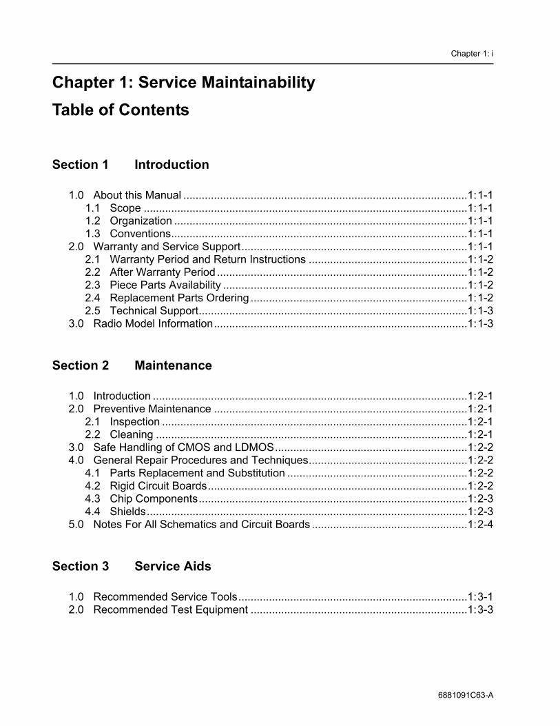
Chapter 1: i
Chapter 1: Service MaintainabilityTable of Contents
Section 1 Introduction
1.0 About this Manual .............................................................................................1:1-11.1 Scope ..........................................................................................................1:1-11.2 Organization ................................................................................................1:1-11.3 Conventions.................................................................................................1:1-1
2.0 Warranty and Service Support..........................................................................1:1-12.1 Warranty Period and Return Instructions ....................................................1:1-22.2 After Warranty Period ..................................................................................1:1-22.3 Piece Parts Availability ................................................................................1:1-22.4 Replacement Parts Ordering .......................................................................1:1-22.5 Technical Support........................................................................................1:1-3
3.0 Radio Model Information...................................................................................1:1-3
Section 2 Maintenance
1.0 Introduction .......................................................................................................1:2-12.0 Preventive Maintenance ...................................................................................1:2-1
2.1 Inspection ....................................................................................................1:2-12.2 Cleaning ......................................................................................................1:2-1
3.0 Safe Handling of CMOS and LDMOS...............................................................1:2-24.0 General Repair Procedures and Techniques....................................................1:2-2
4.1 Parts Replacement and Substitution ...........................................................1:2-24.2 Rigid Circuit Boards.....................................................................................1:2-24.3 Chip Components........................................................................................1:2-34.4 Shields.........................................................................................................1:2-3
5.0 Notes For All Schematics and Circuit Boards ...................................................1:2-4
Section 3 Service Aids
1.0 Recommended Service Tools...........................................................................1:3-12.0 Recommended Test Equipment .......................................................................1:3-3
6881091C63-A
Chapter 1: ii
Notes
6881091C63-A

Chapter 1: 1-1
Section 1INTRODUCTION
1.0 About this Manual
1.1 Scope
This manual is intended for use by service technicians familiar with mobile two-way radio equipment. It contains service information required for the equipment described and is current as of the printing date. Changes which occur after the printing date may be incorporated by a complete manual revision or alternatively as additions.
1.2 Organization
This manual is organized such that the first three chapters contain non–band-specific information, and the remaining chapters cover band-specific information (for example, VHF low power, UHF Band 1 high power, etc.).
All data on control heads—including board overlays, schematics, and parts lists—is contained in Chapter 2, and all data on controllers is in Chapter 3.
The band-specific chapters (Chapters 4–13) each contain their own sections on:
• model charts and technical specifications (Section 1)• theory of operation (Section 2)• troubleshooting charts (Section 3)• board overlays, schematics, and parts lists (Section 4)
Every chapter includes its own table of contents. In addition, the introductory page for each schematics section in the manual has allocation charts, indicating the page numbers for each board overlay, schematic and parts list in the section.
1.3 Conventions
“Microprocessor” is abbreviated as “µP”.
2.0 Warranty and Service SupportMotorola offers support which includes full exchange and/or repair of the product during the warranty period (available only in certain countries), and service/repair or spare parts support out of warranty. Any “return for exchange” or “return for repair” to an authorized Motorola Dealer must be accompanied by a Warranty Claim Form. Contact an authorized Motorola dealer for Warranty Claim Forms.
NOTE Before operating or testing these units, please read the Product Safety and RF Exposurebooklet (Motorola publication part number 6881095C99) enclosed with your radio.
6881091C63-A

Chapter 1: 1-2 Warranty and Service Support
2.1 Warranty Period and Return Instructions
The terms and conditions of warranty are defined fully in the Motorola Dealer or Distributor or Reseller contract. These conditions may change from time to time, and the following subsections are for guidance purposes only.
In instances where the product is covered under a “return for replacement” or “return for repair” warranty, follow the steps outlined below before shipping the unit back to the appropriate Motorola warranty depot:
1. Check the product to make sure it is correctly programmed or has not been subjected to damage outside the terms of the warranty.
2. Contact Customer Resources to report the problem.3. Fill out a Warranty Claim Form. (Forms are available from your Customer Resources
representative or authorized Motorola dealer.)4. Ship the product(s) back in the original packaging (or otherwise securely packaged) to ensure
it is not damaged in transit. Enclose the Warranty Claim Form in the package.
2.2 After Warranty Period
Motorola continues to support its products in two ways after the Warranty period:
• Motorola's Customer Care and Services Division (CCSD) (formerly AAD) offers a repair service to both end-users and dealers at competitive prices.
• CCSD supplies individual parts and modules that can be purchased by dealers who are technically capable of performing fault analysis and repair.
2.3 Piece Parts Availability
Some replacement parts, spare parts, and/or product information can be ordered directly.
2.4 Replacement Parts Ordering
When ordering replacement parts and information, be sure to specify the complete Motorola identification number in your order. Direct all part orders to your local Customer Care and Services Division (CCSD) office. Refer to the Appendix in the back of this manual for contact information.
If... It means that...
The part has a complete Motorola part number assigned to it
The part can be ordered from Motorola’s Customer Care and Services Division.
The part does not have a part number assigned to it
The part is not normally available from Motorola.
The part number is appended with an asterisk The part is serviceable only by a Motorola Depot.
A parts list is not included No user-serviceable parts are available for that kit or assembly.
6881091C63-A
Radio Model Information Chapter 1: 1-3
2.5 Technical Support
Motorola provides technical support to assist dealers, distributors and self-maintained customers in resolving problems, if any, with their unit. When contacting Motorola Technical Support, keep the radio’s model number and the unit’s serial number handy. Technical support contact information is listed below.
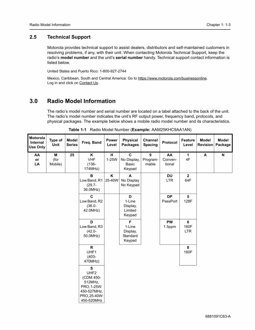
3.0 Radio Model InformationThe radio’s model number and serial number are located on a label attached to the back of the unit. The radio’s model number indicates the unit’s RF output power, frequency band, protocols, and physical packages. The example below shows a mobile radio model number and its characteristics.
Table 1-1 Radio Model Number (Example: AAM25KHC9AA1AN)
United States and Puerto Rico: 1-800-927-2744
Mexico, Caribbean, South and Central America: Go to https://www.motorola.com/businessonline. Log in and click on Contact Us.
Motorola Internal
Use Only
Type of Unit
Model Series Freq. Band Power
LevelPhysical Packages
Channel Spacing Protocol Feature
LevelModel
RevisionModel
Package
AAorLA
M(for
Mobile)
25 KVHF(136-
174MHz)
H1-25W
CNo Display,
Basic Keypad
9Program-
mable
AAConven-
tional
14F
A N
BLow Band, R1
(29.7-36.0MHz)
K25-40W
ANo DisplayNo Keypad
DULTR
264F
CLow Band, R2
(36.0-42.0MHz)
D1-Line
Display, Limited Keypad
DPPassPort
5128F
DLow Band, R3
(42.0-50.0MHz)
F1-Line
Display, Standard Keypad
PW1.5ppm
6160FLTR
RUHF1(403-
470MHz)
8160F
SUHF2
(CDM:450-512MHz,
PRO,1-25W: 450-527MHz, PRO,25-40W:450-520MHz
6881091C63-A

Chapter 1: 1-4 Radio Model Information
6881091C63-A
Notes
Chapter 1: 2-1
Section 2MAINTENANCE
1.0 IntroductionThis chapter of the manual describes:
• preventive maintenance• safe handling of CMOS devices• repair procedures and techniques
2.0 Preventive MaintenanceThe radios do not require a scheduled preventive maintenance program; however, periodic visual inspection and cleaning is recommended.
2.1 Inspection
Check that the external surfaces of the radio are clean, and that all external controls and switches are functional. We recommend against inspecting the interior electronic circuitry.
2.2 Cleaning
The following procedures describe the recommended cleaning agents and the methods to be used when cleaning the external and internal surfaces of the radio. External surfaces include the front cover, housing assembly, and battery case. These surfaces should be cleaned whenever a periodic visual inspection reveals the presence of smudges, grease, and/or grime.
2.2.1 Cleaning External Plastic Surfaces
The only recommended agent for cleaning the external radio surfaces is a 0.5% solution of a mild dishwashing detergent in water. Apply this solution sparingly on the surface with a stiff, non-metallic, short-bristled brush to work all loose dirt out. Use a soft, absorbent, lintless cloth or tissue to remove the solution. Then dry the radio. Make sure that no water remains entrapped near the connectors, cracks, or crevices.
The effects of certain chemicals and their vapors can have harmful results on certain plastics. Do not use aerosol sprays, tuner cleaners, and other chemicals to clean the radio.
NOTE Internal surfaces should be cleaned only when the radio is disassembled for servicing orrepair.
!C a u t i o n
6881091C63-A

Chapter 1: 2-2 Safe Handling of CMOS and LDMOS
2.2.2 Cleaning Internal Circuit Boards and Components
The only factory-recommended liquid for cleaning the printed circuit boards and their components is isopropyl alcohol (100% by volume). Apply Isopropyl alcohol with a stiff, non-metallic, short-bristled brush to dislodge embedded or caked materials located in hard-to-reach areas. The brush stroke should direct the dislodged material out and away from the inside of the radio. Make sure that controls or tunable components are not soaked with alcohol. Do not use high-pressure air to hasten the drying process since this could cause the liquid to collect in unwanted places. Upon completion of the cleaning process, use a soft, absorbent, lintless cloth to dry the area. Do not brush or apply any isopropyl alcohol to the frame, front cover, or back cover.
3.0 Safe Handling of CMOS and LDMOSComplementary metal-oxide semiconductor (CMOS) devices are used in this family of radios. CMOS characteristics make them susceptible to damage by electrostatic or high voltage charges. Damage can be latent, resulting in failures occurring weeks or months later. Therefore, take special precautions to prevent device damage during disassembly, troubleshooting, and repair.
Handling precautions are mandatory for CMOS circuits and are especially important in low humidity conditions.
4.0 General Repair Procedures and Techniques
4.1 Parts Replacement and Substitution
When replacing damaged parts, use identical part replacements. If an identical replacement component is not locally available, check the parts list for the proper Motorola part number and order the component from the nearest Motorola parts center (see the Appendix at the back of this manual).
4.2 Rigid Circuit Boards
This family of radios uses bonded, multi-layer, printed circuit boards. Since the inner layers are not accessible, some special considerations are required when soldering and desoldering components. The through-plated holes may interconnect multiple layers of the printed circuit. Therefore, exercise care to avoid pulling the plated circuit out of the hole.
When soldering near the 18-pin and 40-pin connectors:
• avoid accidentally getting solder in the connector. • be careful not to form solder bridges between the connector pins.• closely examine your work for shorts due to solder bridges.
NOTE Always use a fresh supply of alcohol and a clean container to prevent contamination bydissolved material (from previous usage).
DO NOT attempt to disassemble the radio without first referring to the disassembly and reassembly sections in the Basic Service Manual (Motorola Publication part number 6881091C62 [CDM Series models] or 6881092C71 [PRO Series models]).!
C a u t i o n
6881091C63-A

General Repair Procedures and Techniques Chapter 1: 2-3
4.3 Chip ComponentsUse either the RLN4062 Hot-Air Repair Station or the Motorola 0180381B45 Repair Station for chip component replacement. When using the 0180381B45 Repair Station, select the TJ-65 mini-thermojet hand piece. On either unit, adjust the temperature control to 370°C (700°F), and adjust the airflow to a minimum setting. Airflow can vary due to component density.
To remove a chip component:
1. Use a hot-air hand piece and position the nozzle of the hand piece approximately 0.3 cm (1⁄8") above the component to be removed.
2. Begin applying the hot air. Once the solder reflows, remove the component using a pair of tweezers.
3. Using a solder wick and a soldering iron or a power desoldering station, remove the excess solder from the pads.
To replace a chip component using a soldering iron:
1. Select the appropriate micro-tipped soldering iron and apply fresh solder to one of the solder pads.
2. Using a pair of tweezers, position the new chip component in place while heating the fresh solder.
3. Once solder wicks onto the new component, remove the heat from the solder. 4. Heat the remaining pad with the soldering iron and apply solder until it wicks to the
component. If necessary, touch up the first side. All solder joints should be smooth and shiny.
To replace a chip component using hot air:
1. Use the hot-air hand piece and reflow the solder on the solder pads to smooth it. 2. Apply a drop of solder paste flux to each pad. 3. Using a pair of tweezers, position the new component in place. 4. Position the hot-air hand piece approximately 0.3 cm (1/8") above the component and begin
applying heat. 5. Once the solder wicks to the component, remove the heat and inspect the repair. All joints
should be smooth and shiny.
4.4 ShieldsRemove and replace shields using the R1070 station with the temperature control set to approximately 215°C (415°F) [230°C (445°F) maximum].
To remove the shield:
1. Place the circuit board in the R1070 circuit board holder. 2. Select the proper heat focus head and attach it to the heater chimney. 3. Add solder paste flux around the base of the shield. 4. Position the shield under the heat-focus head. 5. Lower the vacuum tip and attach it to the shield by turning on the vacuum pump. 6. Lower the focus head until it is approximately 0.3 cm (1/8") above the shield. 7. Turn on the heater and wait until the shield lifts off the circuit board. 8. Once the shield is off, turn off the heat, grab the part with a pair of tweezers, and turn off the
vacuum pump. 9. Remove the circuit board from the R1070 circuit-board holder.
6881091C63-A
Chapter 1: 2-4 Notes For All Schematics and Circuit Boards
To replace the shield:
1. Add solder to the shield, if necessary, using a micro-tipped soldering iron. 2. Rub the soldering iron tip along the edge of the shield to smooth out any excess solder. Use
solder wick and a soldering iron to remove excess solder from the solder pads on the circuit board.
3. Place the circuit board back in the R1070 circuit board holder. 4. Place the shield on the circuit board using a pair of tweezers. 5. Position the heat-focus head over the shield and lower it to approximately 0.3 cm (1/8") above
the shield.6. Turn on the heater and wait for the solder to reflow.7. Once complete, turn off the heat, raise the heat-focus head, and wait approximately one
minute for the part to cool. 8. Remove the circuit board and inspect the repair. No cleaning should be necessary.
5.0 Notes For All Schematics and Circuit Boards* Component is frequency sensitive. Refer to the Electrical Parts List for value and usage.
• Unless otherwise stated, resistances are in Ohms (K = 1000, M = 1,000,000), and capacitances are in picofarads (pF), nanofarads (nF), or microfarads (µF).
• DC voltages are measured from point indicated to chassis ground using a Motorola DC multimeter or equivalent. Transmitter measurements should be made with a 1.2 µH (microHenry) choke in series with the voltage probe to prevent circuit loading.
• Interconnect Tie Point Legend:
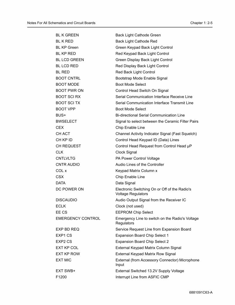
16_8MHz 16.8MHz Reference Frequency3V3 Regulated 3.3V Supply Voltage for Voice Storage5V Regulated 5V Supply Voltage for RF Circuitry5V Regulated 5V Supply Voltage (Control Head)5V RF Regulated 5V Supply Voltage for RF Circuitry5V SOURCE 5V Signal to Switch On Control Head5VD Regulated 5V Supply Voltage for Digital Circuitry9V3 Regulated 9.3V Supply Voltage9V3FLT Filtered 9.3V Supply VoltageA+ 13.2V Supply VoltageADDR Microprocessor (µP) Address LinesAN Analog Lines to Analog-to-Digital ConverterANALOG INPUT 2 External Keypad Matrix Column SignalANALOG INPUT 3 External Keypad Matrix Row SignalBATTERY VOLTAGE Battery Voltage Sense LineBL A GREEN Back Light Anode GreenBL A RED Back Light Anode RedBL GREEN Green Back Light Control
6881091C63-A
Notes For All Schematics and Circuit Boards Chapter 1: 2-5
BL K GREEN Back Light Cathode GreenBL K RED Back Light Cathode RedBL KP Green Green Keypad Back Light ControlBL KP RED Red Keypad Back Light ControlBL LCD GREEN Green Display Back Light ControlBL LCD RED Red Display Back Light ControlBL RED Red Back Light ControlBOOT CNTRL Bootstrap Mode Enable SignalBOOT MODE Boot Mode SelectBOOT PWR ON Control Head Switch On SignalBOOT SCI RX Serial Communication Interface Receive LineBOOT SCI TX Serial Communication Interface Transmit LineBOOT VPP Boot Mode SelectBUS+ Bi-directional Serial Communication LineBWSELECT Signal to select between the Ceramic Filter PairsCEX Chip Enable Line CH ACT Channel Activity Indicator Signal (Fast Squelch)CH KP ID Control Head Keypad ID (Data) LinesCH REQUEST Control Head Request from Control Head µPCLK Clock SignalCNTLVLTG PA Power Control VoltageCNTR AUDIO Audio Lines of the ControllerCOL x Keypad Matrix Column xCSX Chip Enable Line DATA Data SignalDC POWER ON Electronic Switching On or Off of the Radio's
Voltage RegulatorsDISCAUDIO Audio Output Signal from the Receiver ICECLK Clock (not used)EE CS EEPROM Chip SelectEMERGENCY CONTROL Emergency Line to switch on the Radio's Voltage
RegulatorsEXP BD REQ Service Request Line from Expansion BoardEXP1 CS Expansion Board Chip Select 1EXP2 CS Expansion Board Chip Select 2EXT KP COL External Keypad Matrix Column SignalEXT KP ROW External Keypad Matrix Row SignalEXT MIC External (from Accessory Connector) Microphone
InputEXT SWB+ External Switched 13.2V Supply VoltageF1200 Interrupt Line from ASFIC CMP
6881091C63-A
Chapter 1: 2-6 Notes For All Schematics and Circuit Boards
FECTRL 1 Control Voltage for Front-End Filter FECTRL 2 Control Voltage for Front-End Attenuator SwitchFLASH CS Flash Chip SelectFLASH OE Flash Output EnableFLAT RX SND Option Board Audio Output SignalFLAT TX RTN Flat TX Input from Option Board and Accessory
ConnectorFLT A+ Filtered 13.2 V Supply VoltageGP x IN General Purpose Input xGP x IN ACC y General Purpose Input x from Accessory
Connector Pin yGP x IN OUT ACC y General Purpose Input/Output x from Accessory
Connector Pin yGP x OUT General Purpose Output xGP x OUT ACC y General Purpose Input x from Accessory
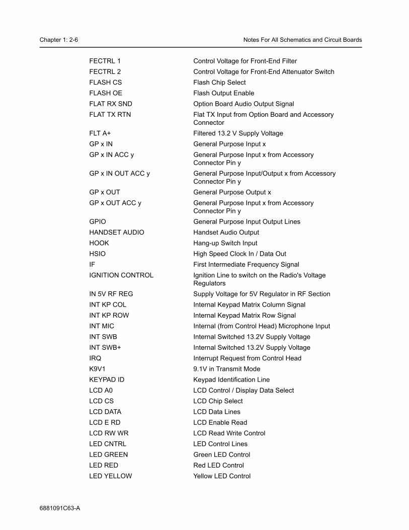
Connector Pin yGPIO General Purpose Input Output LinesHANDSET AUDIO Handset Audio OutputHOOK Hang-up Switch InputHSIO High Speed Clock In / Data OutIF First Intermediate Frequency SignalIGNITION CONTROL Ignition Line to switch on the Radio's Voltage
RegulatorsIN 5V RF REG Supply Voltage for 5V Regulator in RF SectionINT KP COL Internal Keypad Matrix Column SignalINT KP ROW Internal Keypad Matrix Row SignalINT MIC Internal (from Control Head) Microphone InputINT SWB Internal Switched 13.2V Supply VoltageINT SWB+ Internal Switched 13.2V Supply VoltageIRQ Interrupt Request from Control HeadK9V1 9.1V in Transmit ModeKEYPAD ID Keypad Identification LineLCD A0 LCD Control / Display Data SelectLCD CS LCD Chip SelectLCD DATA LCD Data LinesLCD E RD LCD Enable ReadLCD RW WR LCD Read Write ControlLED CNTRL LED Control LinesLED GREEN Green LED ControlLED RED Red LED ControlLED YELLOW Yellow LED Control
6881091C63-A
Notes For All Schematics and Circuit Boards Chapter 1: 2-7
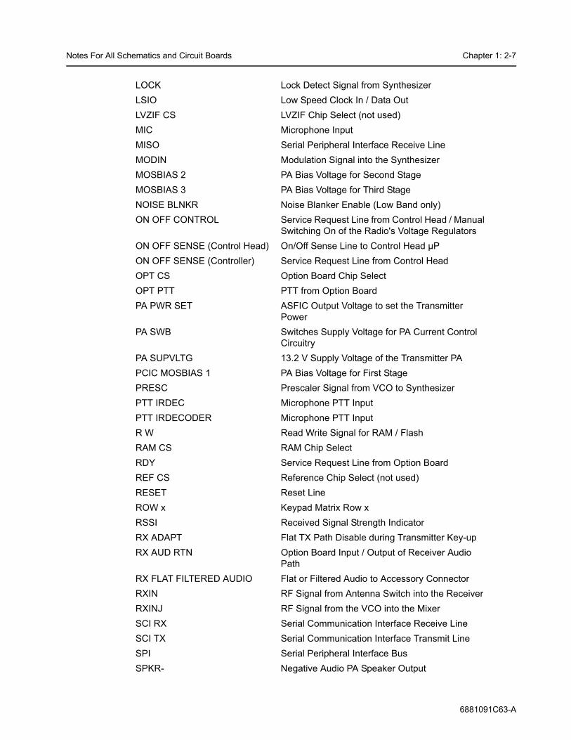
LOCK Lock Detect Signal from SynthesizerLSIO Low Speed Clock In / Data OutLVZIF CS LVZIF Chip Select (not used)MIC Microphone InputMISO Serial Peripheral Interface Receive LineMODIN Modulation Signal into the SynthesizerMOSBIAS 2 PA Bias Voltage for Second StageMOSBIAS 3 PA Bias Voltage for Third StageNOISE BLNKR Noise Blanker Enable (Low Band only)ON OFF CONTROL Service Request Line from Control Head / Manual
Switching On of the Radio's Voltage RegulatorsON OFF SENSE (Control Head) On/Off Sense Line to Control Head µPON OFF SENSE (Controller) Service Request Line from Control HeadOPT CS Option Board Chip SelectOPT PTT PTT from Option BoardPA PWR SET ASFIC Output Voltage to set the Transmitter
PowerPA SWB Switches Supply Voltage for PA Current Control
CircuitryPA SUPVLTG 13.2 V Supply Voltage of the Transmitter PAPCIC MOSBIAS 1 PA Bias Voltage for First StagePRESC Prescaler Signal from VCO to SynthesizerPTT IRDEC Microphone PTT InputPTT IRDECODER Microphone PTT InputR W Read Write Signal for RAM / FlashRAM CS RAM Chip SelectRDY Service Request Line from Option BoardREF CS Reference Chip Select (not used)RESET Reset LineROW x Keypad Matrix Row xRSSI Received Signal Strength IndicatorRX ADAPT Flat TX Path Disable during Transmitter Key-upRX AUD RTN Option Board Input / Output of Receiver Audio
PathRX FLAT FILTERED AUDIO Flat or Filtered Audio to Accessory ConnectorRXIN RF Signal from Antenna Switch into the ReceiverRXINJ RF Signal from the VCO into the MixerSCI RX Serial Communication Interface Receive LineSCI TX Serial Communication Interface Transmit LineSPI Serial Peripheral Interface BusSPKR- Negative Audio PA Speaker Output
6881091C63-A
Chapter 1: 2-8 Notes For All Schematics and Circuit Boards
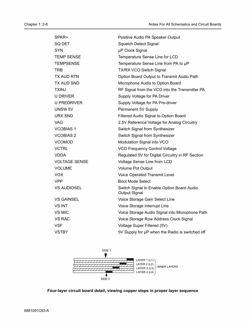
Four-layer circuit board detail, viewing copper steps in proper layer sequence
SPKR+ Positive Audio PA Speaker OutputSQ DET Squelch Detect SignalSYN µP Clock SignalTEMP SENSE Temperature Sense Line for LCDTEMPSENSE Temperature Sense Line from PA to µPTRB TX/RX VCO Switch SignalTX AUD RTN Option Board Output to Transmit Audio PathTX AUD SND Microphone Audio to Option BoardTXINJ RF Signal from the VCO into the Transmitter PAU DRIVER Supply Voltage for PA DriverU PREDRIVER Supply Voltage for PA Pre-driverUNSW 5V Permanent 5V SupplyURX SND Filtered Audio Signal to Option BoardVAG 2.5V Reference Voltage for Analog CircuitryVCOBIAS 1 Switch Signal from SynthesizerVCOBIAS 2 Switch Signal from SynthesizerVCOMOD Modulation Signal into VCOVCTRL VCO Frequency Control VoltageVDDA Regulated 5V for Digital Circuitry in RF SectionVOLTAGE SENSE Voltage Sense Line from LCDVOLUME Volume Pot OutputVOX Voice Operated Transmit LevelVPP Boot Mode SelectVS AUDIOSEL Switch Signal to Enable Option Board Audio
Output SignalVS GAINSEL Voice Storage Gain Select LineVS INT Voice Storage Interrupt LineVS MIC Voice Storage Audio Signal into Microphone PathVS RAC Voice Storage Row Address Clock SignalVSF Voltage Super Filtered (5V)VSTBY 5V Supply for µP when the Radio is switched off
LAYER 1 (L1)LAYER 2 (L2)LAYER 3 (L3)LAYER 4 (L4)
INNER LAYERS
SIDE 1
SIDE 2
6881091C63-A
Chapter 1: 3-1
Section 3SERVICE AIDS
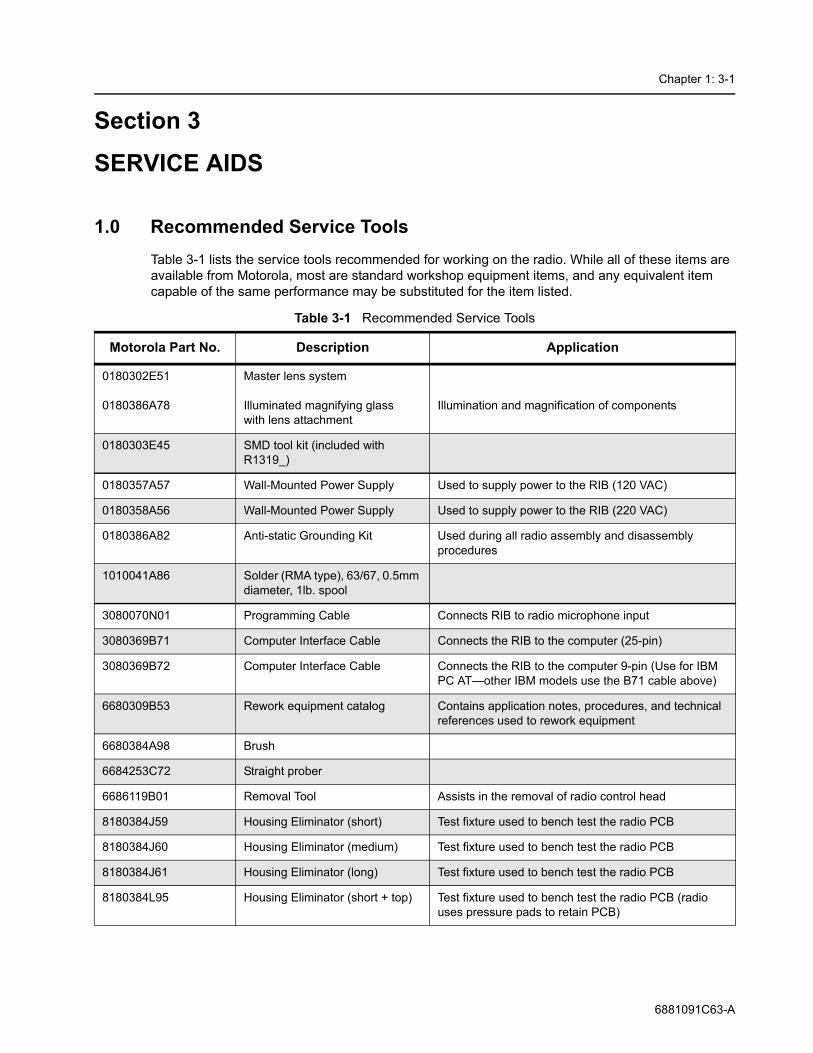
1.0 Recommended Service ToolsTable 3-1 lists the service tools recommended for working on the radio. While all of these items are available from Motorola, most are standard workshop equipment items, and any equivalent item capable of the same performance may be substituted for the item listed.
Table 3-1 Recommended Service Tools
Motorola Part No. Description Application
0180302E51
0180386A78
Master lens system
Illuminated magnifying glasswith lens attachment
Illumination and magnification of components
0180303E45 SMD tool kit (included with R1319_)
0180357A57 Wall-Mounted Power Supply Used to supply power to the RIB (120 VAC)
0180358A56 Wall-Mounted Power Supply Used to supply power to the RIB (220 VAC)
0180386A82 Anti-static Grounding Kit Used during all radio assembly and disassembly procedures
1010041A86 Solder (RMA type), 63/67, 0.5mm diameter, 1lb. spool
3080070N01 Programming Cable Connects RIB to radio microphone input
3080369B71 Computer Interface Cable Connects the RIB to the computer (25-pin)
3080369B72 Computer Interface Cable Connects the RIB to the computer 9-pin (Use for IBM PC AT—other IBM models use the B71 cable above)
6680309B53 Rework equipment catalog Contains application notes, procedures, and technical references used to rework equipment
6680384A98 Brush
6684253C72 Straight prober
6686119B01 Removal Tool Assists in the removal of radio control head
8180384J59 Housing Eliminator (short) Test fixture used to bench test the radio PCB
8180384J60 Housing Eliminator (medium) Test fixture used to bench test the radio PCB
8180384J61 Housing Eliminator (long) Test fixture used to bench test the radio PCB
8180384L95 Housing Eliminator (short + top) Test fixture used to bench test the radio PCB (radio uses pressure pads to retain PCB)
6881091C63-A
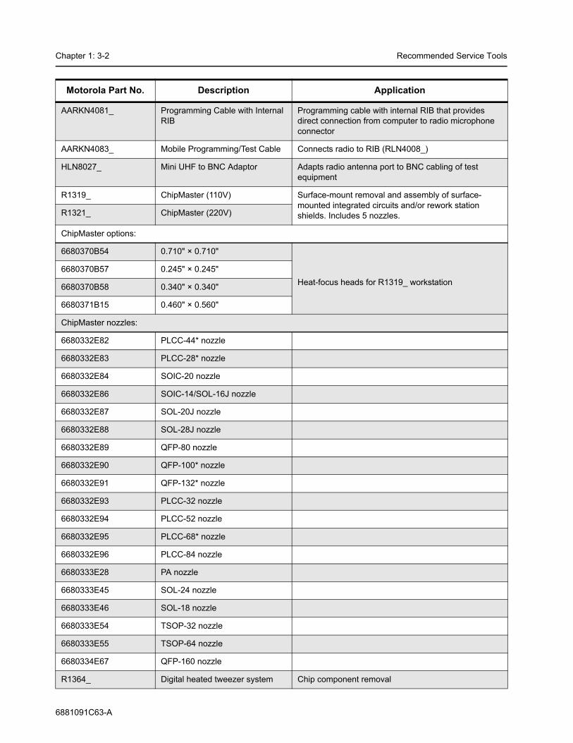
Chapter 1: 3-2 Recommended Service Tools
AARKN4081_ Programming Cable with Internal RIB
Programming cable with internal RIB that provides direct connection from computer to radio microphone connector
AARKN4083_ Mobile Programming/Test Cable Connects radio to RIB (RLN4008_)
HLN8027_ Mini UHF to BNC Adaptor Adapts radio antenna port to BNC cabling of test equipment
R1319_ ChipMaster (110V) Surface-mount removal and assembly of surface-mounted integrated circuits and/or rework station shields. Includes 5 nozzles.R1321_ ChipMaster (220V)
ChipMaster options:
6680370B54 0.710" × 0.710"
Heat-focus heads for R1319_ workstation6680370B57 0.245" × 0.245"
6680370B58 0.340" × 0.340"
6680371B15 0.460" × 0.560"
ChipMaster nozzles:
6680332E82 PLCC-44* nozzle
6680332E83 PLCC-28* nozzle
6680332E84 SOIC-20 nozzle
6680332E86 SOIC-14/SOL-16J nozzle
6680332E87 SOL-20J nozzle
6680332E88 SOL-28J nozzle
6680332E89 QFP-80 nozzle
6680332E90 QFP-100* nozzle
6680332E91 QFP-132* nozzle
6680332E93 PLCC-32 nozzle
6680332E94 PLCC-52 nozzle
6680332E95 PLCC-68* nozzle
6680332E96 PLCC-84 nozzle
6680333E28 PA nozzle
6680333E45 SOL-24 nozzle
6680333E46 SOL-18 nozzle
6680333E54 TSOP-32 nozzle
6680333E55 TSOP-64 nozzle
6680334E67 QFP-160 nozzle
R1364_ Digital heated tweezer system Chip component removal
Motorola Part No. Description Application
6881091C63-A
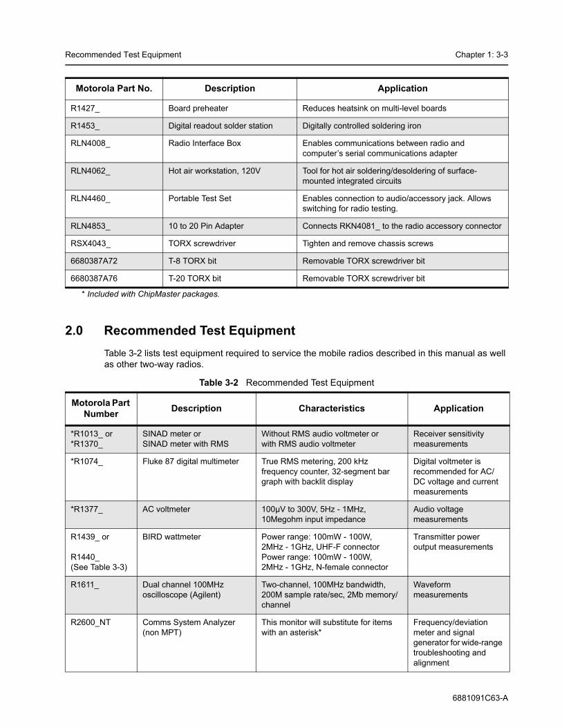
Recommended Test Equipment Chapter 1: 3-3
* Included with ChipMaster packages.
2.0 Recommended Test EquipmentTable 3-2 lists test equipment required to service the mobile radios described in this manual as well as other two-way radios.
Table 3-2 Recommended Test Equipment
R1427_ Board preheater Reduces heatsink on multi-level boards
R1453_ Digital readout solder station Digitally controlled soldering iron
RLN4008_ Radio Interface Box Enables communications between radio and computer’s serial communications adapter
RLN4062_ Hot air workstation, 120V Tool for hot air soldering/desoldering of surface-mounted integrated circuits
RLN4460_ Portable Test Set Enables connection to audio/accessory jack. Allows switching for radio testing.
RLN4853_ 10 to 20 Pin Adapter Connects RKN4081_ to the radio accessory connector
RSX4043_ TORX screwdriver Tighten and remove chassis screws
6680387A72 T-8 TORX bit Removable TORX screwdriver bit
6680387A76 T-20 TORX bit Removable TORX screwdriver bit
Motorola Part Number Description Characteristics Application
*R1013_ or *R1370_
SINAD meter orSINAD meter with RMS
Without RMS audio voltmeter orwith RMS audio voltmeter
Receiver sensitivity measurements
*R1074_ Fluke 87 digital multimeter True RMS metering, 200 kHz frequency counter, 32-segment bar graph with backlit display
Digital voltmeter is recommended for AC/DC voltage and current measurements
*R1377_ AC voltmeter 100µV to 300V, 5Hz - 1MHz, 10Megohm input impedance
Audio voltage measurements
R1439_ or
R1440_(See Table 3-3)
BIRD wattmeter Power range: 100mW - 100W, 2MHz - 1GHz, UHF-F connectorPower range: 100mW - 100W, 2MHz - 1GHz, N-female connector
Transmitter power output measurements
R1611_ Dual channel 100MHz oscilloscope (Agilent)
Two-channel, 100MHz bandwidth, 200M sample rate/sec, 2Mb memory/channel
Waveform measurements
R2600_NT Comms System Analyzer (non MPT)
This monitor will substitute for items with an asterisk*
Frequency/deviation meter and signal generator for wide-range troubleshooting and alignment
Motorola Part No. Description Application
6881091C63-A
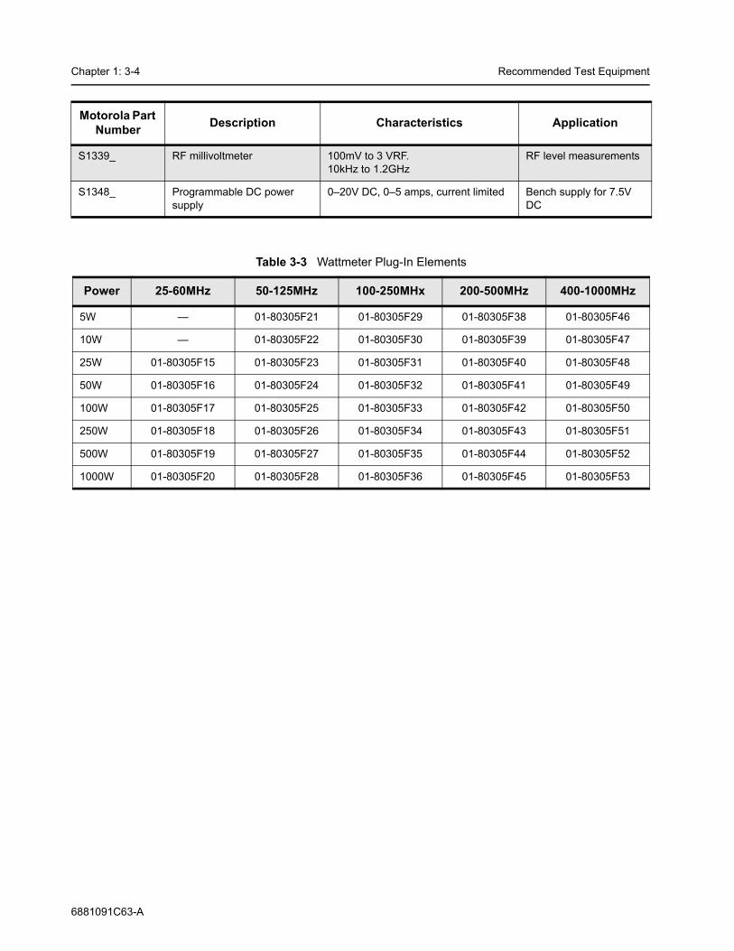
Chapter 1: 3-4 Recommended Test Equipment
S1339_ RF millivoltmeter 100mV to 3 VRF.10kHz to 1.2GHz
RF level measurements
S1348_ Programmable DC power supply
0–20V DC, 0–5 amps, current limited Bench supply for 7.5V DC
Table 3-3 Wattmeter Plug-In Elements
Power 25-60MHz 50-125MHz 100-250MHx 200-500MHz 400-1000MHz
5W — 01-80305F21 01-80305F29 01-80305F38 01-80305F46
10W — 01-80305F22 01-80305F30 01-80305F39 01-80305F47
25W 01-80305F15 01-80305F23 01-80305F31 01-80305F40 01-80305F48
50W 01-80305F16 01-80305F24 01-80305F32 01-80305F41 01-80305F49
100W 01-80305F17 01-80305F25 01-80305F33 01-80305F42 01-80305F50
250W 01-80305F18 01-80305F26 01-80305F34 01-80305F43 01-80305F51
500W 01-80305F19 01-80305F27 01-80305F35 01-80305F44 01-80305F52
1000W 01-80305F20 01-80305F28 01-80305F36 01-80305F45 01-80305F53
Motorola Part Number Description Characteristics Application
6881091C63-A
Chapter 2: i
Chapter 2: Control Head Service InformationTable of Contents
Section 1 Overview
1.0 CDM750 / PRO3100 Model (GCN6112_).........................................................2:1-12.0 CDM1250 / PRO5100 Model (GCN6113_).......................................................2:1-13.0 CDM1550 Series / PRO7100 Model (GCN6114_)............................................2:1-2
Section 2 Theory of Operation
1.0 Introduction .......................................................................................................2:2-12.0 Control Head (CDM750 / PRO3100) ................................................................2:2-1
2.1 Power Supplies............................................................................................2:2-12.2 Power On/Off...............................................................................................2:2-12.3 Microprocessor Circuit.................................................................................2:2-12.4 SBEP Serial Interface..................................................................................2:2-22.5 Keypad Keys ...............................................................................................2:2-22.6 Status LED and Back Light Circuit...............................................................2:2-32.7 Microphone Connector Signals ...................................................................2:2-32.8 Speaker .......................................................................................................2:2-32.9 Electrostatic Transient Protection ................................................................2:2-4
3.0 Control Head (CDM1250 / PRO5100 / CDM1550 Series / PRO7100) .............2:2-43.1 Power Supplies............................................................................................2:2-43.2 Power On/Off...............................................................................................2:2-43.3 Microprocessor Circuit.................................................................................2:2-43.4 SBEP Serial Interface..................................................................................2:2-53.5 Keypad Keys ...............................................................................................2:2-53.6 Status LED and Back Light Circuit ..............................................................2:2-63.7 Liquid Crystal Display (LCD) .......................................................................2:2-63.8 Microphone Connector Signals ...................................................................2:2-73.9 Speaker .......................................................................................................2:2-73.10 Electrostatic Transient Protection................................................................2:2-73.11 PassPort Trunking Controller Board (PTCB)...............................................2:2-8
Section 3 Troubleshooting Charts
1.0 Control Head CDM750 / PRO3100 Troubleshooting Flow Charts....................2:3-11.1 Troubleshooting Flow Chart for On/Off........................................................2:3-1
6881091C63-A

Chapter 2: ii
1.2 Troubleshooting Flow Chart for Microprocessor ........................................2:3-22.0 Control Head CDM1250 / PRO5100 / CDM1550 Series / PRO7100
Troubleshooting Flow Charts............................................................................2:3-32.1 Troubleshooting Flow Chart for On/Off ......................................................2:3-32.2 Troubleshooting Flow Chart for Microprocessor .........................................2:3-42.3 Troubleshooting Flow Chart for Display ......................................................2:3-52.4 Troubleshooting Flow Chart for Back Light .................................................2:3-6
Section 4 Control Head PCBs, Schematics, and Parts Lists
1.0 Allocation of Schematics and Circuit Boards ....................................................2:4-12.0 Control Head CDM750 / PRO3100 PCB 8486146B07, Schematics, and
Parts Lists ........................................................................................................2:4-33.0 Control Head CDM1250 / PRO5100 / CDM1550 Series / PRO7100 PCB
8486155B06, Schematics, and Parts Lists .......................................................2:4-7
6881091C63-A

Chapter 2: 1-1
Section 1OVERVIEW
1.0 CDM750 / PRO3100 Model (GCN6112_)This control head (Model A) contains the internal speaker, the On/Off/Volume knob, the microphone connector, buttons to operate the radio, and indicator Light Emitting Diodes (LEDs) to indicate radio status. The radio uses a Motorola 68HC11E9 microprocessor to control the LEDs and communicate with the host radio.
Model A Control Head (GCN6112_) for CDM750 / PRO3100
2.0 CDM1250 / PRO5100 Model (GCN6113_)This control head (Model B) contains the internal speaker, the On/Off/Volume knob, the microphone connector, buttons to operate the radio, LEDs to indicate radio status, and a 14-character Liquid Crystal Display (LCD) that displays alphanumerical information (for example, channel number or call address name). The radio uses a Motorola 68HC11E9 microprocessor to control the LEDs and LCD, and communicate with the host radio.
Model B Control Head (GCN6113_) for CDM1250 / PRO5100
6881091C63-A
Chapter 2: 1-2 CDM1550 Series / PRO7100 Model (GCN6114_)
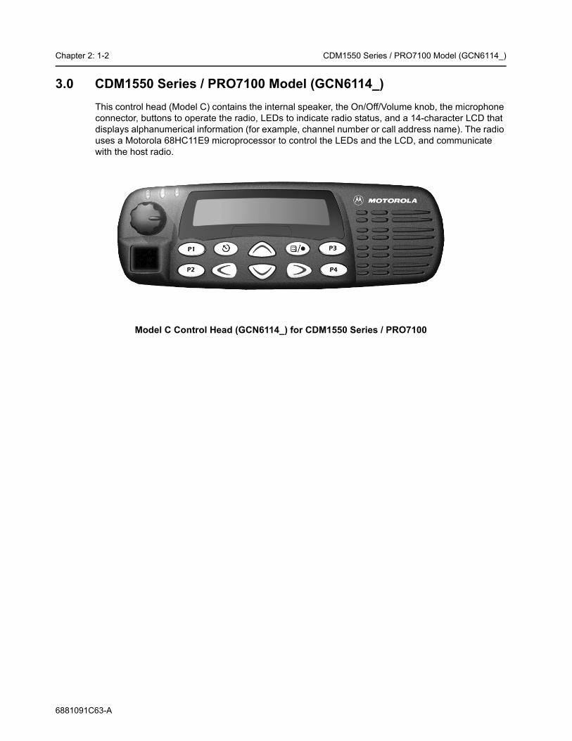
3.0 CDM1550 Series / PRO7100 Model (GCN6114_)This control head (Model C) contains the internal speaker, the On/Off/Volume knob, the microphone connector, buttons to operate the radio, LEDs to indicate radio status, and a 14-character LCD that displays alphanumerical information (for example, channel number or call address name). The radio uses a Motorola 68HC11E9 microprocessor to control the LEDs and the LCD, and communicate with the host radio.
Model C Control Head (GCN6114_) for CDM1550 Series / PRO7100
6881091C63-A

Chapter 2: 2-1
Section 2THEORY OF OPERATION
1.0 IntroductionThis chapter provides a detailed theory of operation for the control head circuits. For troubleshooting information, refer to the related section of this manual.
2.0 Control Head (CDM750 / PRO3100)
2.1 Power SuppliesThe power supply to the control head is taken from the host radio’s FLT A+ voltage via connector J0801, pin 3 and the regulated 5V via connector J0801 pin 7. The voltage FLT A+ is at battery level and is used for the LEDs, the back light and to power up the radio using the On/Off/Volume knob. The stabilized 5V is used for the µP and the keypad buttons. The voltage USW 5V derived from the FLT A+ voltage and stabilized by the series combination of R0822, VR0822 is used to buffer the internal RAM of the µP (U0831). C0822 allows the battery voltage to be disconnected for a couple of seconds without losing RAM parameters. Dual diode D0822 prevents radio circuits from discharging this capacitor. When the supply voltage is applied to the radio, C0822 is charged via R0822 and D0822. To avoid the µP entering the wrong mode if the radio is switched on while the voltage across C0822 is still too low, the regulated 5V supply charges C0822 via diode D0822.
2.2 Power On/OffThe On/Off/Volume knob, when pressed, switches the radio’s voltage regulators on by connecting line ON OFF CONTROL to line UNSW 5V via D0821. Additionally, 5V at the base of digital transistor Q0822 informs the control head’s µP about the pressed knob. The µP asserts pin 62 and line CH REQUEST low to hold the line ON OFF CONTROL at 5V via Q0823 and D0821. The high line ON OFF CONTROL also informs the host radio that the control head’s µP wants to send data via the SBEP bus. When the radio returns a data request message, the µP informs the radio about the pressed knob. If the radio is switched off, the radio’s µP switches it on and vice versa. If the On/Off/Volume knob is pressed while the radio is on, the software detects a low state on line ON OFF SENSE, the radio is alerted via line ON OFF CONTROL and sends a data request message. The control head µP informs the radio about the pressed knob and the radio’s µP switches the radio off.
2.3 Microprocessor CircuitThe control head uses the Motorola 68HC11E9 µP (U0831) to control the LEDs and to communicate with the host radio. RAM and ROM are contained within the µP.
The µP generates its clock using the oscillator inside the µP along with a 8 MHz ceramic resonator (U0833) and R0920.
The µP’s RAM is always powered to maintain parameters such as the last operating mode. This is achieved by maintaining 5V at µP, pin 25. Under normal conditions, when the radio is off, USW 5V is formed by FLT A+ running to D0822. Capacitor C0822 allows the battery voltage to be disconnected
NOTE From this point on the microprocessor is referred to as “µP”.
6881091C63-A

Chapter 2: 2-2 Control Head (CDM750 / PRO3100)
for a couple of seconds without losing RAM parameters. Diode D0822 prevents radio circuits from discharging this capacitor.
There are eight analog-to-digital converter ports (A/D) on the µP. They are labeled within the device block as PE0-PE7. These lines sense the voltage level ranging from 0 to 5V of the input line and convert that level to a number ranging from 0 to 255 which can be read by the software to take appropriate action.
Pin VRH is the high reference voltage for the A/D ports on the µP. If this voltage is lower than 5V the A/D reading is incorrect. The VRL signal is the low reference for the A/D ports. This line is normally tied to ground. If this line is not connected to ground, the A/D readings could be incorrect.
The µP determines the used keypad type and the control head ID by reading the levels at ports PC0 – PC7. Connections JU0852/3/4 are provided by the individual keypads.
The MODB / MODA input of the µP must be at a logic “1” to start executing correctly. The XIRQ and the IRQ pins should also be at a logic “1”.
Voltage sense device U0832 provides a reset output that goes to 0V if the regulated 5V goes below 4.5 V. This is used to reset the controller to prevent improper operation.
2.4 SBEP Serial InterfaceThe host radio (master) communicates to the control head µP (slave) through its SBEP bus. This bus uses only line BUS+ for data transfer. The line is bi-directional, that is, either the radio or the control head µP can drive the line. The µP sends serial data via pin 50 and D0831 and it reads serial data via pin 47. Whenever the µP detects activity on the BUS+ line, it starts communication.
When the host radio needs to communicate to the control head µP, it sends data via line BUS+. Any transition on this line generates an interrupt and the µP starts communication. The host radio may send data (for example, LED and back light status) or it may request the control head ID or the keypad ID.
When the control head µP wants to communicate to the host radio, the µP brings the request line CH REQUEST to a logic “0” via µP pin 62. This switches Q0823 on, which pulls line ON OFF CONTROL high through diode D0821. A low-to-high transition on this line informs the radio that the control head requires service. The host radio then sends a data request message via BUS+ and the control head µP replies with the data it wants to send (for example, which key has been pressed or that the volume knob has been rotated).
The control head µP monitors all messages sent via BUS+, but ignores any data communication between the host radio and the CPS or the universal tuner.
2.5 Keypad KeysThe control head keypad is a six-key design. All keys are configured as two analog lines read by µP pins 13 and 15. The voltage on the analog lines varies between 0V and 5V depending on which key is pressed. If no key is pressed, the voltage at both lines is 5V. The key configuration can be thought of as a matrix where the two lines represent one row and one column. Each line is connected to a resistive divider powered by 5V. If a button is pressed, it will connect one specific resistor of each divider line to ground level and thereby reduce the voltages on the analog lines The voltages of the lines are A/D converted inside the µP (ports PE 0 - 1) and specify the pressed button. To determine which key is pressed, the voltage of both lines must be considered.
An additional pair of analog lines and A/D µP ports (PE 3 – 2) are available to support a keypad microphone, connected to the microphone connector J0811. Any microphone key press is processed the same way as a key press on a control head.
6881091C63-A

Control Head (CDM750 / PRO3100) Chapter 2: 2-3
2.6 Status LED and Back Light CircuitAll indicator LEDs (red, yellow, and green) are driven by current sources. To change the LED status the host radio sends a data message via SBEP bus to the control head µP. The control head µP determines the LED status from the received message and switches the LEDs on or off via port PB 7 – 0 and port PA4. The LED status is stored in the µP’s memory. The LED current is determined by the resistor at the emitter of the respective current source transistor.
The back light for the keypad is controlled by the host radio the same way as the indicator LEDs using µP port PA 5. The µP can switch the back light on and off under software control. The back light current for the keypad is drawn from the FLT A+ source and controlled by two current sources. The LED current is determined by the resistor at the emitter of the respective current source transistor.
2.7 Microphone Connector SignalsSignals BUS+, PTT IRDEC, HOOK, MIC, HANDSET AUDIO, FLT A+, 5V, and two A/D converter inputs are available at the microphone connector J0811. Signal BUS+ (J0811-7) connects to the SBEP bus for communication with the CPS or the Universal Tuner. Line MIC (J0811-5) feeds the audio from the microphone to the radio’s controller via connector J0801-4. The Line HANDSET AUDIO (J0811-8) feeds the receiver audio from the controller (J0801-6) to a connected handset. FLT A+, which is at supply voltage level, and 5V are used to supply any connected accessory like a microphone or a handset.
The two A/D converter inputs (J0811-9/10) are used for a microphone with keypad. A pressed key changes the DC voltage on both lines. The voltages depend on which key is pressed. The µP determines from the voltage on these lines which key is pressed and sends the information to the host radio.
Line PTT IRDEC (J0811-6) is used to key up the radio’s transmitter. While the PTT button on a connected microphone is released, line PTT IRDEC is pulled to 5V level by R0843. Transistor Q0843 is switched on and causes a low at µP port PA2. When the PTT button is pressed, signal PTT IRDEC is pulled to ground level. This switches Q0843 off and the resulting high level at µP port PA2 signals the µP about the pressed PTT button. The µP signals the host radio about any status change on the PTT IRDEC line via SBEP bus.
When the line PTT IRDEC is connected to FLT A+ level, transistor Q0821 is switched on through diode VR0821 and thereby pulls the level on line ON OFF CONTROL to FLT A+ level. This switches on the radio and puts the radio’s µP in bootstrap mode. Bootstrap mode loads the firmware into the radio’s flash memory.
When the microphone’s hang-up switch is engaged, the HOOK input (J0811-3) signals the µP. Depending on how the radio is programmed using the Customer Programming Software (CPS), the µP may take actions such as turning the audio PA on or off. While the hang-up switch is open, R0841 pulls the line HOOK to a 5V level. Transistor Q0841 is switched on and causes a low at µP port PA1. When the HOOK switch is closed, the HOOK signal is pulled to ground level. This switches R0841 off and the resulting high level at µP port PA1 signals the µP about the closed hang-up switch. The µP signals the host radio about any status change on the HOOK line via the SBEP bus.
2.8 SpeakerThe control head contains a speaker for the receiver audio. The receiver audio signal from the differential audio output of the audio amplifier, located on the radio’s controller, is fed via connector J0801-10, 11 to the speaker connector P0801, pins 1 and 2. The speaker is connected to the
6881091C63-A
Chapter 2: 2-4 Control Head (CDM1250 / PRO5100 / CDM1550 Series / PRO7100)
speaker connector P0801. The control head speaker can be disconnected only if an external speaker (connected through the accessory connector) is used.
2.9 Electrostatic Transient ProtectionElectrostatic transient protection is provided for the sensitive components in the control head by diodes VR0811, VR00812, and VR0816 - VR0817. The diodes limit any transient voltages. The associated capacitors provide radio frequency interference (RFI) protection.
3.0 Control Head (CDM1250 / PRO5100 / CDM1550 Series / PRO7100)
3.1 Power SuppliesThe power supply to the control head is taken from the host radio’s FLT A+ voltage via connector J0801 pin 3 and the regulated 5V via connector J0801 pin 7. The voltage FLT A+ is at battery level and is used for the LEDs, the back light and to power up the radio using the On/Off/Volume knob. The stabilized 5V is used for the µP, the display, the display driver and the keypad buttons. The voltage USW 5V derived from the FLT A+ voltage and stabilized by the series combination of R0822, VR0822 is used to buffer the internal RAM of the µP (U0831). C0822 allows the battery voltage to be disconnected for a couple of seconds without losing RAM parameters. Dual diode D0822 prevents radio circuitry from discharging this capacitor. When the supply voltage is applied to the radio, C0822 is charged via R0822 and D0822. To avoid the µP entering the wrong mode when the radio is switched on while the voltage across C0822 is still too low, the regulated 5V supply charges C0822 via diode D0822.
3.2 Power On/OffThe On/Off/Volume knob, when pressed, switches the radio’s voltage regulators on by connecting line ON OFF CONTROL to line UNSW 5V via D0821. Additionally, 5V at the base of digital transistor Q0822 signals the control head’s µP about the pressed knob. The µP asserts pin 62 and line CH REQUEST low to hold line ON OFF CONTROL at 5V via Q0823 and D0821. The high line ON OFF CONTROL also informs the host radio that the control head’s µP wants to send data via SBEP bus. When the radio returns a data request message, the µP will inform the radio about the pressed knob. If the radio was switched off, the radio’s µP will switch it on and vice versa. If the On/Off/Volume knob is pressed while the radio is on, the software detects a low state on line ON OFF SENSE, the radio is alerted via line ON OFF CONTROL, and sends a data request message. The control head µP will inform the radio about the pressed knob and the radio’s µP will switch the radio off.
3.3 Microprocessor CircuitThe control head uses the Motorola 68HC11E9 µP (U0831) to control the LEDs and the LCD and to communicate with the host radio. RAM and ROM are contained within the µP itself.
The µP generates its clock using the oscillator inside the µP along with a 8 MHz ceramic resonator (U0833) and R0920.
The µP’s RAM is always powered to maintain parameters such as the last operating mode. This is achieved by maintaining 5V at µP pin 25. Under normal conditions, when the radio is off, USW 5V is formed by FLT A+ running to D0822. C0822 allows the battery voltage to be disconnected for a couple of seconds without losing RAM parameters. Diode D0822 prevents radio circuitry from discharging this capacitor.
There are eight analog-to-digital converter ports (A/D) on the µP. They are labeled within the device block as PE0-PE7. These lines sense the voltage level ranging from 0 to 5V of the input line and
6881091C63-A
Control Head (CDM1250 / PRO5100 / CDM1550 Series / PRO7100) Chapter 2: 2-5
convert that level to a number ranging from 0 to 255 which can be read by the software to take appropriate action.
Pin VRH is the high-reference voltage for the A/D ports on the µP. If this voltage is lower than 5V, the A/D readings will be incorrect. Likewise pin VRL is the low reference for the A/D ports. This line is normally tied to ground. If this line is not connected to ground, the A/D readings will be incorrect.
The µP can determine the keypad type and the control head ID by reading the levels at ports PC0 – PC7. Connections JU0852/3/4 are provided by individual keypads.
The MODB / MODA input of the µP must be at a logic “1” for it to start executing correctly. The XIRQ and the IRQ pins should also be at a logic “1”.
Voltage sense device U0832 provides a reset output that goes to 0V if the regulated 5V goes below 4.5 V. This is used to reset the controller to prevent improper operation.
3.4 SBEP Serial InterfaceThe host radio (master) communicates to the control head µP (slave) through its SBEP bus. This bus uses only line BUS+ for data transfer. The line is bi-directional, that is, either the radio or the control head µP can drive the line. The µP sends serial data via pin 50 and D0831 and it reads serial data via pin 47. Whenever the µP detects activity on the BUS+ line, it starts communication.
When the host radio needs to communicate to the control head µP, it sends data via line BUS+. Any transition on this line generates an interrupt and the µP starts communication. The host radio may send data (for example, display information, LED status, or back light status), or it may request the control head or keypad ID.
When the control head µP wants to communicate to the host radio, the µP brings request line CH REQUEST to a logic “0” via µP pin 62. This switches on Q0823, which pulls line ON OFF CONTROL high through diode D0821. A low-to-high transition on this line informs the radio that the control head requires service. The host radio then sends a data request message via BUS+ and the control head µP replies with the data it wants to send (for example, which key has been pressed or that the volume knob has been rotated).
The control head µP monitors all messages sent via BUS+, but ignores any data communication between host radio and CPS or Universal Tuner.
3.5 Keypad KeysThe control head keypad is a six-key keypad (Model B) or a 10-key keypad (Model C). All keys are configured as two analog lines read by µP pins 13 and 15. The voltage on the analog lines varies between 0V and 5V depending on the key that has been pressed. If no key is pressed, the voltage at both lines will be 5V. The key configuration can be thought of as a matrix where the two lines represent one row and one column. Each line is connected to a resistive divider powered by 5V. If a button is pressed, it will connect one specific resistor of each divider line to ground level and thereby reduce the voltages on the analog lines. The voltages of the lines are A/D converted inside the µP (ports PE 0 - 1) and specify the pressed button. The voltage of both lines must be considered in order to determine which key is pressed.
An additional pair of analog lines and A/D µP ports (PE 3 – 2) is available to support a keypad microphone, connected to the microphone connector J0811. Any microphone key press is processed in the same way as a key press on the control head.
6881091C63-A
Chapter 2: 2-6 Control Head (CDM1250 / PRO5100 / CDM1550 Series / PRO7100)
3.6 Status LED and Back Light CircuitAll indicator LEDs (red, yellow, and green) are driven by current sources. To change the LED status the host radio sends a data message via SBEP bus to the control head µP. The control head µP determines the LED status based the received message and switches the LEDs on or off via port PB 7 – 0 and port PA4. The LED status is stored in the µP’s memory. The LED current is determined by the resistor at the emitter of the respective current source transistor.
The back light for the LCD and the keypad is controlled by the host radio the same way as the indicator LEDs using µP port PA 5. This port is a Pulse Width Modulator (PWM) output. The output signal charges capacitor C0843 through R0847. By changing the pulse width under software control, the DC voltage of C0843 and, therefore, the brightness of the back light can be changed in four steps. The keypad back light current is drawn from the FLT A+ source and controlled by transistor Q0933. The current flowing through the LEDs causes a proportional voltage drop across the parallel resistors R0947 and R0948. This voltage drop is amplified by the op-amp U0931-2. U0931-2 and Q0934 form a differential amplifier. The voltage difference between the base of Q0934 and the output of U0931-2 determines the current from the base of the LED control transistor Q0933 and in turn the brightness of the LEDs. The µP can control the LEDs by changing the DC level at the base of Q0934. If the base of Q0934 is at ground level, Q0934 is switched off and no current flows through Q0933 and the LEDs. If the base voltage of Q0934 rises, a current flows through Q0934 and in turn through Q0933, causing the LEDs to turn on and a rising voltage drop across R0947 and R0948. The rising voltage causes the output of the op-amp to rise and to reduce the base to emitter voltage of Q0934. This decreases the current of Q0933 until the loop has settled.
3.7 Liquid Crystal Display (LCD)The LCD H0971 uses the display driver U0971. The display is a single-layer super-twist nematic (STN) LCD display. It has 14 characters and a 5x8 dot matrix to display alphanumerical information and a line with 21 pre-defined icons above the dot matrix.
The driver contains a data interface to the µP, an LCD segment driver, an LCD power circuit, an oscillator, data RAM and control logic. At power up, the driver’s control logic is reset by a logic “0” at input SR2 (U0971-15). The driver’s internal oscillator is set to about 20 kHz and can be measured at pin 22. The driver’s µP interface is configured to accept 8-bit parallel data input (U0971-D0-D7) from the control head µP (U0831 port PC0-PC7).
To write data to the driver’s RAM, the µP sets chip select (U0971-20) to logic “0” via U0831-11, RD (U0971-18) to logic “1” via (U0831-10) and WR (U0971-17) to logic “0” via U0831-9. With input A0 (U0971-21) set to logic “0” via U0831-12, the µP writes control data to the driver. Control data includes the RAM start address for the display data. With input A0 set to logic “1”, the µP then writes the display data to the display RAM. When data transfer is complete, the µP terminates the chip select, RD and WD activities.
The display driver’s power circuit provides the voltage supply for the display. This circuit consists of a voltage multiplier, voltage regulator and a voltage follower. The external capacitors C0971 - C0973 configure the multiplier to double the supply voltage. In this configuration, the multiplier output VOUT (U0971-8) supplies a voltage of –5V (2* –5V below VDD). The multiplied voltage VOUT is sent to the internal voltage regulator. To set the voltage level of the regulator output V5 (U0971-5), this voltage is divided by the resistors R0973 and R0974 and then fed back to the reference input VR (U0971-6). In addition, the regulator output voltage V5 can be controlled electronically by a control command sent to the driver. With the used configuration, the voltage V5 is about –2V. The voltage V5 is resistively divided by the driver’s voltage follower to provide the voltages V1 - V4. These voltages are required to drive the liquid crystals. The level of V5 can be measured by one of the µP’s analog-to-digital converters (U0831-20) via resistive divider R0975, R0976. To stabilize the display brightness over a large temperature range, the µP measures the temperature via analog-to-digital
6881091C63-A
Control Head (CDM1250 / PRO5100 / CDM1550 Series / PRO7100) Chapter 2: 2-7
converter (U0831-18) using temperature sensor U0834. Based on the measured temperature, the µP adjusts the driver output voltage V5, and in turn the display brightness, via a parallel interface.
3.8 Microphone Connector SignalsSignals BUS+, PTT IRDEC, HOOK, MIC, HANDSET AUDIO, FLT A+, 5V and 2 A/D converter inputs are available at the microphone connector J0811. Signal BUS+ (J0811-7) connects to the SBEP bus for communication with the CPS or the Universal Tuner. Line MIC (J0811-5) feeds the audio from the microphone to the radio’s controller via connector J0801-4. Line HANDSET AUDIO (J0811-8) feeds the receiver audio from the controller (J0801-6) to a connected handset. FLT A+, which is at supply voltage level, and 5V are used to supply accessories connected to the radio, if any (for example, a microphone or a handset).
The two A/D converter inputs (J0811-9/10) are used for a microphone with a keypad. When a key is pressed, the DC voltage changes on both lines. The voltages depend on which key is pressed. The µP determines which key is pressed based on the voltage on these lines. It then sends the information to the host radio.
Line PTT IRDEC (J0811-6) is used to key up the radio’s transmitter. When the PTT button on a connected microphone is released, line PTT IRDEC is pulled to 5V level by R0843. Transistor Q0843 is switched on and causes a low at µP port PA2. When the PTT button is pressed, signal PTT IRDEC is pulled to ground level. This switches Q0843 off and the resulting high level at µP port PA2 signals the µP about the pressed PTT button. The µP informs the host radio about any change of status on the PTT IRDEC line via SBEP bus.
When line PTT IRDEC is connected to FLT A+ level, transistor Q0821 is switched on through diode VR0821 and thereby pulls the level on line ON OFF CONTROL to FLT A+ level. This switches the radio on and puts the radio’s µP in bootstrap mode. Bootstrap mode is the mode used to load the firmware into the radio’s flash memory (see the Controller chapter for more details).
The HOOK input (J0811-3) is used to signal the µP when the microphone’s hang-up switch is engaged. Depending on the CPS programming the µP may take actions like turning the audio PA on or off. While the hang-up switch is open, line HOOK is pulled to 5V level by R0841. Transistor Q0841 is switched on and causes a low at µP port PA1. When the HOOK switch is closed, signal HOOK is pulled to ground level. This switches off R0841 and the resulting high level at µP port PA1 informs the µP about the closed hang-up switch. The µP will inform the host radio about any status change on the HOOK line via SBEP bus.
3.9 SpeakerThe control head contains a speaker for receiver audio. The receiver audio signal from the differential audio output of the audio amplifier (located on the radio’s controller) is fed via connector J0801-10, 11 to the speaker connector P0801 pin 1 and pin 2. The speaker is connected to the speaker connector P0801. The control head speaker can be disconnected if an external speaker (connected through the accessory connector) is used.
3.10 Electrostatic Transient ProtectionElectrostatic transient protection is provided for the sensitive components in the control head by diodes VR0811, VR00812, and VR0816 - VR0817. The diodes limit any transient voltages to tolerable levels. The associated capacitors provide Radio Frequency Interference (RFI) protection.
6881091C63-A
Chapter 2: 2-8 Control Head (CDM1250 / PRO5100 / CDM1550 Series / PRO7100)
3.11 PassPort Trunking Controller Board (PTCB)PassPort is an enhanced trunking protocol developed by Trident Microsystems that supports wide-area dispatch networking. A network is formed by linking several trunked sites together to form a single system. This offers users an extended communication coverage area. Additionally, users with PassPort can seamlessly roam among all sites within the network. Seamless roaming means that the radio user does not have to manually change the position on the radio when roaming from site to site.
For models which feature PassPort Trunking operation, the PassPort Trunking Controller Board (PTCB) is added to the top cover of the radio. This board also provides advanced voice storage features. Refer to Figure 2-1 for connector and signal routing from and to the radio and PTCB.
Figure 2-1 Full Serial Interface Lines for PassPort Trunking Controller Board
PassPort BoardMain Radio Board (68HC11)
J601-26
J601-25
J601-38
J601-12
J601-11
Serial Data Send Serial Data Return
Serial Data Return Serial Data Send
Serial Clock Send Serial Clock Line
Data Ready/Request Data Ready/Request
Option Board Enable Option Board Enable
Voice StorageJ601-6 J601-10
Flat Tx Return
Flat Rx Send
6881091C63-A
Chapter 2: 3-1
6881091C63-A
Section 3TROUBLESHOOTING CHARTS
1.0 Control Head CDM750 / PRO3100 Troubleshooting Flow Charts1.1 Troubleshooting Flow Chart for On/Off
Radio does not turn on when On/Off/Volume Knob is pressed
NO
YES
YES
NO
R0823 Pin TAB= 5V?
R0823 Pin TAB1when pressed
= 5V?
Check / Replace Volume Pot R0823
Check / ReplaceR0822 / VR0822 /
D0822 / C0822
NO
YESJ0801 Pin 2
> 10V?
Check / ReplaceQ0821
Check / ReplaceQ0822 / R0821
YES
NOJ0801 Pin 2
=5V?
Check / ReplaceD0821 / R0852
Press and holdOn/Off/Volume Knob
Chapter 2: 3-2 Control Head CDM750 / PRO3100 Troubleshooting Flow Charts
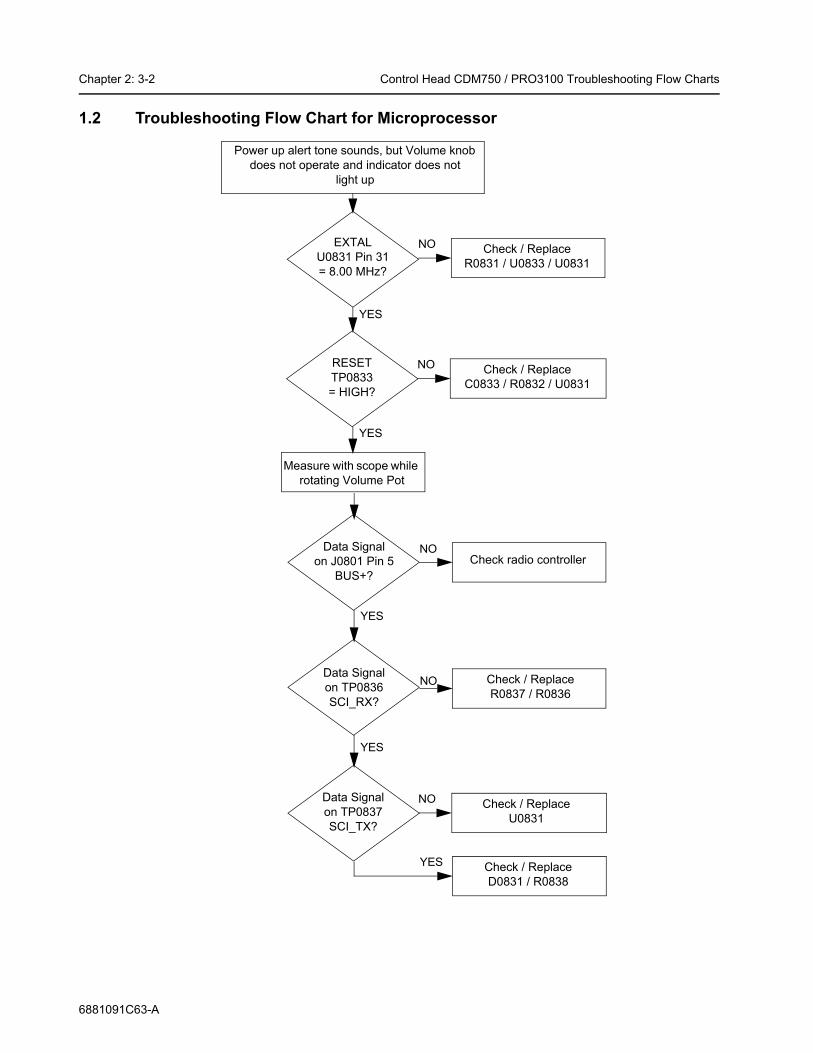
1.2 Troubleshooting Flow Chart for Microprocessor
Power up alert tone sounds, but Volume knob does not operate and indicator does not
light up
NO
YES
YES
NO
YES
NO
YES
NO
YES
EXTALU0831 Pin 31= 8.00 MHz?
RESETTP0833= HIGH?
Check / ReplaceC0833 / R0832 / U0831
Check radio controllerData Signal
on J0801 Pin 5BUS+?
Data Signal on TP0836SCI_RX?
NO
Data Signalon TP0837SCI_TX?
Check / ReplaceR0831 / U0833 / U0831
Check / ReplaceR0837 / R0836
Check / ReplaceU0831
Check / ReplaceD0831 / R0838
Measure with scope while rotating Volume Pot
6881091C63-A

Control Head CDM1250 / PRO5100 / CDM1550 Series / PRO7100 Troubleshooting Flow Charts Chapter 2: 3-3
2.0 Control Head CDM1250 / PRO5100 / CDM1550 Series / PRO7100 Troubleshooting Flow Charts
2.1 Troubleshooting Flow Chart for On/Off Radio does not turn on when On/Off/Volume Knob is
pressed
NO
YES
YES
NO
R0823 Pin TAB= 5V?
R0823 Pin TAB1when pressed
= 5V?
Check / Replace Volume Pot R0823
Check / ReplaceR0822 / VR0822 /
D0822 / C0822
NO
YESJ0801 Pin 2
> 10V?Check / Replace
Q0821
Check / ReplaceQ0822 / R0821
YES
NOJ0801 Pin 2=5V?
Check / ReplaceD0821 / R0852
Press and holdOn/Off/Volume Knob
6881091C63-A
Chapter 2: 3-4 Control Head CDM1250 / PRO5100 / CDM1550 Series / PRO7100 Troubleshooting Flow Charts
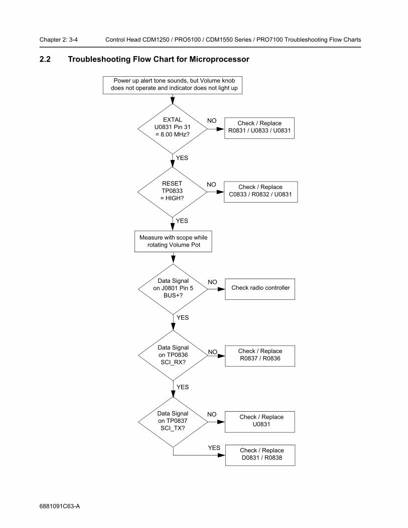
2.2 Troubleshooting Flow Chart for Microprocessor
Power up alert tone sounds, but Volume knob does not operate and indicator does not light up
NO
YES
YES
NO
YES
NO
YES
NO
YES
EXTALU0831 Pin 31= 8.00 MHz?
RESETTP0833= HIGH?
Check / ReplaceC0833 / R0832 / U0831
Check radio controllerData Signal
on J0801 Pin 5BUS+?
Data Signalon TP0836SCI_RX?
NO
Data Signalon TP0837SCI_TX?
Check / ReplaceR0831 / U0833 / U0831
Check / ReplaceR0837 / R0836
Check / ReplaceU0831
Check / ReplaceD0831 / R0838
Measure with scope while rotating Volume Pot
6881091C63-A

Control Head CDM1250 / PRO5100 / CDM1550 Series / PRO7100 Troubleshooting Flow Charts Chapter 2: 3-5
2.3 Troubleshooting Flow Chart for Display
Power up alert tone sounds, Volume knob works,indicator/back light is on, but the display is blank
YES
NO
YES
NO
V5 (against 5V)TP0973 between
-6V and -7V?
Activity onAddress & Data lines
A0 / D0..D7 / CS1of U0971?
Check for shortU0831 / U0971
Check LCD Assembly
Check / ReplaceC0971 / C0973 / R0972R0973 / R0974 / U0971
6881091C63-A
Chapter 2: 3-6 Control Head CDM1250 / PRO5100 / CDM1550 Series / PRO7100 Troubleshooting Flow Charts
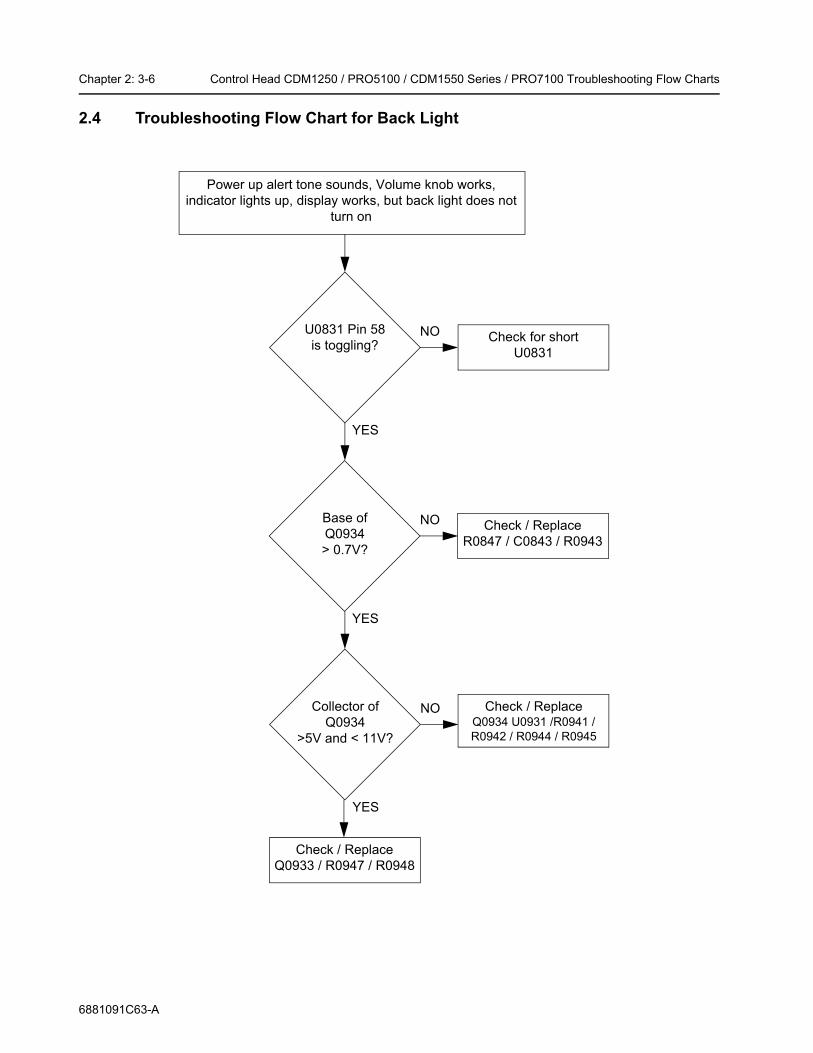
2.4 Troubleshooting Flow Chart for Back Light
Power up alert tone sounds, Volume knob works,indicator lights up, display works, but back light does not
turn on
NO
YES
YES
NO
U0831 Pin 58is toggling?
Base of Q0934> 0.7V?
Check / Replace R0847 / C0843 / R0943
Check for shortU0831
YES
NOCollector ofQ0934
>5V and < 11V?
Check / ReplaceQ0934 U0931 /R0941 / R0942 / R0944 / R0945
Check / ReplaceQ0933 / R0947 / R0948
6881091C63-A
Chapter 2: 4-1
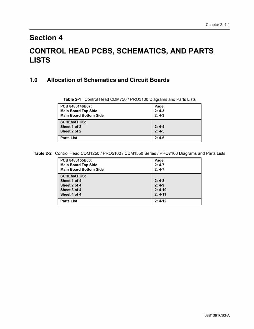
Section 4CONTROL HEAD PCBS, SCHEMATICS, AND PARTS LISTS
1.0 Allocation of Schematics and Circuit Boards
Table 2-1 Control Head CDM750 / PRO3100 Diagrams and Parts ListsPCB 8486146B07:Main Board Top SideMain Board Bottom Side
Page:2: 4-32: 4-3
SCHEMATICS:Sheet 1 of 2Sheet 2 of 2
2: 4-42: 4-5
Parts List 2: 4-6
Table 2-2 Control Head CDM1250 / PRO5100 / CDM1550 Series / PRO7100 Diagrams and Parts ListsPCB 8486155B06:Main Board Top SideMain Board Bottom Side
Page:2: 4-72: 4-7
SCHEMATICS:Sheet 1 of 4Sheet 2 of 4Sheet 3 of 4Sheet 4 of 4
2: 4-82: 4-92: 4-102: 4-11
Parts List 2: 4-12
6881091C63-A

Chapter 2: 4-2 Allocation of Schematics and Circuit Boards
Notes
6881091C63-A
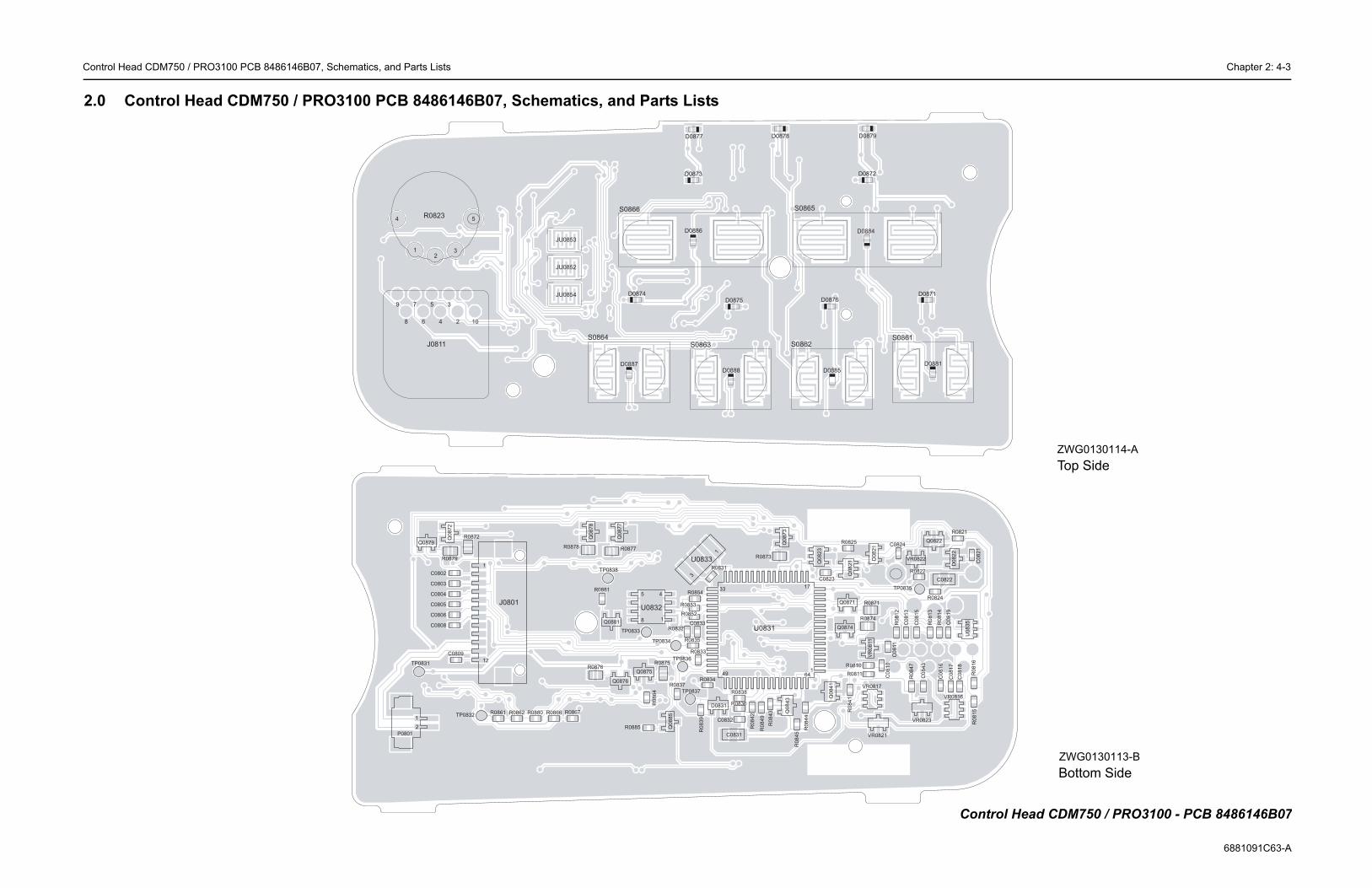
Control Head CDM750 / PRO3100 PCB 8486146B07, Schematics, and Parts Lists Chapter 2: 4-3
6881091C63-A
2
D0871
D0872
6
D0879
D0881
D0884
5
S0861
C0
81
0
C0
811
C0
81
3
C0
81
5
C0
81
6
C0
81
7
C0
81
8
C0
81
9
C0
82
1
C0822
C0824
C0
84
3
D0
82
1
D0
82
2
Q0
82
1
Q0822
Q0871
Q0874
R0810
R0811
R0
81
2
R0
81
3
R0
81
4
R0
81
5R
08
16
R0821
R0822
R0824
R0825
R0
84
1
R0
84
7
R0871
R0874
TP0835
U0
83
5
VR
08
11
VR0816
VR0817
VR0821
VR0822
VR0823
Control Head CDM750 / PRO3100 - PCB 8486146B07
Top Side
Bottom SideZWG0130113-B
ZWG0130114-A
.0 Control Head CDM750 / PRO3100 PCB 8486146B07, Schematics, and Parts Lists
D0873
D0874D0875 D087
D0877 D0878
D088
D0886
D0887D0888
2
3579
8 6 4 10
J0811
JU0852
JU0853
JU0854
4
12
3
5R0823
S0862S0863S0864
S0865S0866
C0802
C0803
C0804
C0805
C0806
C0808
C0809
C0823
C0831
C0832
C0833
D0831
12
J0801
1
2
P0801
Q0
82
3
Q0
84
1
Q0
84
3
Q0
87
2
Q0
87
3
Q0875
Q0876
Q0
87
7
Q0
87
8
Q0879
Q0881
Q0
88
5
R0832
R0833
R0834
R0835
R0836
R0837
R0838
R0
83
9
R0
84
2
R0
84
3
R0
84
4
R0
84
5
R0
84
9
R0852
R0853
R0854
R0861 R0862
R0
86
4
R0866 R0867
R0872
R0873
R0875R0876
R0877R0878
R0879
R0880
R0881
R0885
TP0831
TP0832
TP0833
TP0834
TP0836
TP0837
TP0838
149
1733
U0831
1
45
8
U0832
364
1
1
R0831
U0833

Chapter 2: 4-4 Control Head CDM750 / PRO3100 PCB 8486146B07, Schematics, and Parts Lists
688109
47K
47K47K
47K
CONTROL HEAD
CONNECTOR
J0801
CONTROLLER
KEYPAD ID
CONTROL HEAD ID
R08432.2K
7
J0801-8
JU0853SWITCH
2
10KR0844
55
VD
D22
VR
H2
1V
RL
23
VS
S1
VS
S2
24
49
VS
S3
XIRQ
XTAL
PE3_AN3
PE4_AN4
PE5_AN5
PE6_AN6
PE7_AN7
RESET
28STRA_AS
30STRB_RW*
PD1_TXD
PD2_MISO
PD3_MOSI
PD4_SCK
PD5_SS*
PE0_AN0
PE1_AN1
PE2_AN2
PC1_AD136
PC2_AD237
PC3_AD338
PC4_AD439
40PC5_AD5
PC6_AD641
PC7_AD742
PD0_RXD
PB1_A911
PB2_A1010
PB3_A119
PB4_A128
7PB5_A13
PB6_A146
PB7_A15 5
PC0_AD034
64PA1_IC2
63PA2_IC1
62PA3_OC5_OC1
59PA4_OC4_OC1
58PA5_OC3_OC1
57PA6_OC2_OC1
56PA7_PA1_OC1
PB0_A812
NC
34
NC
42
6N
C5
32
35
NC
644
NC
7
NC
84
86
0N
C9
1PA0_IC3
CLK_E
EXTAL
IRQ
MODA_LIR*
MODB_VSTBY
NC
12
NC
10
61
3N
C2
MC
68
HC
71
1E
9
U0831
7
J0801-11
J0801-7
3
10
Q0843F2
1
2
06
2
C0809
NU
82pF
4
5
100KR0853
8
0
P0801-2
54
J0801-9
J0801-10
J0801-6
JU0852SWITCHJU0854
6
1
SWITCH
C0804
470pF
0
R0852100K
7
R08454.7K
NU
C0808
470pF470pFC0806
10K
3
R0841
4
47K
J0801-14
R0849
P0801-1
J0801-3
J0801-5
3 2
100KR0854
6
1
J0801-12
J0801-4
5
J0801-13
J0801-1
NU
J0801-2
470pFC0802
C0803470pF
C080582pF
R084247K
Q0841
5V
CH_KP_ID(0:7)
LED_CNTRL(0:8)
CH_REQUEST
5V
5V
PTT_IRDECPT
SCI_TX
BL_GREEN
ON_OFF_SENSE
5V
HOOK
ON_OFF_CONTROL
FLT_A+
MIC
BUS+
HANDSET_AUDIO
5V
ZWG0130239-BContr
1C63-A
47K
47K
HOOK
GROUND
MIC
10GM300
PTT_IRDECODER
789
MICROPHONE
CONNECTOR
SCI_RX
BOOT_VPP
J0811
RESET
BOOT_MODE
WARIS
HANDSET_AUDIO
1
SCI_TX
EXT_KP_ROW
EXT_KP_COL
FLT_A+
456
BUS+
23 5V
VR08225.6V
NU
GND
INPUT RESET_
U0835MC33464N-45ATR
C0833
R0833
0.1uF
47K
45
33
1914
16
1820
43
50
51
52
53
54
13
15
17
47
29
31
46
2725
TP083250K
NEG
POS TAB
TAB1
VA
R
R0823
4.7K
R0824
J0811-5
NU
R0835100
0R0839
R0847
22
J0811-4
270
R0814
R0815
0.1uC083
13K
C08313.3uF
J0811-1
C0823.01uF
Q0823
D0822
10R0813
1C1
3C2
2
GN
D
R0812
CSTCC8.00MGU0833
22
5.6V
VR0821
5.6V
VR0823
J0811-10
TP0837
INPUT2
NC13
NC25 NC3
6
NC478
NC5
RESET1
U0832MC33064
GND
4
Q0821
J0811-6
C081782pF
J0811-8
NU
VR081133V
470pF
NU470pF
C0818
C0816
33KR0837
R081151K
J0811-3
J0811-2
1MEGR0831
VR081620V
13K
J0811-9
R0810
TP0833
10KR0821
2.2KR0832
TP0838
TP0834
NU
470pF
NU
C0810470pF
C0819
R083810K
J0811-7
R0834
270
20VVR0817
2.2uFC0822
470pFNU
13K
C0821
R0816
R0822
51K470pF
C0815
C0811470pF
TP0831
R083610K
TP0836
470pFC0843 C0813
TP0835
470pF
NU
C0824
.01uF
R0825
1K
D0821
Q0822INT_KP_ROW
INT_KP_COL
USW_5V
5V
5V
5V
5V
FLT_A+
BUS+
EXT_KP_ROW
MIC
EXT_KP_COL
FLT_A+
D0831
CH_REQUEST
5V
5V
5V
HOOK
ON_OFF_SENSE
ON_OFF_CONTROL
5V
USW_5V
VOLUME
VOLUMEEXT_KP_ROW
EXT_KP_COL
T_IRDEC
FLT_A+
FLT_A+
5V
5V
PTT_IRDEC
SCI_TX
BUS+
5V
5V
5V
5V
HANDSET_AUDIO
Shown from Front Side
ol Head CDM750 / PRO3100 - Schematic Sheet 1 of 2

Control Head CDM750 / PRO3100 PCB 8486146B07, Schematics, and Parts Lists Chapter 2: 4-5
6881091C63-A
LED5LED4 LED6LED1 LED2 LED3
greenD0885
greenD0888
D0886green
greenD0887
greenD0884
greenD0881
270R0885
270R0881
Q0885
270
green
R0877
D0877 D0879
Q0877
red
270R0878
Q0879Q0878
yellowD0878
Q0873
R0879270
R0871270
Q0871 Q0872
82
redD0876
7
D0875redred
D0874
R0876270
R0875270
R0874
Q0876
270
Q0875Q0874
6
W
5
4 3
red
Q0881
D0872 D087red red
R087
D0871
270
1 0
R0872
FLT_A+
LED_CNTRL(0:8)
BL_GREEN
FLT_A+
FLT_A+
LED_CNTRL(0:8)
270
Control Head CDM750 / PRO3100 - Schematic Sheet 2 of 2
ZWG0130240-A
S0862
F4 P2
F3 P1
F2
F1
F1 F2 F3 F4
P1 P2
LED1 LED2 LED3
1V/1V
0V/0V
0V/1V
LED4
LED6 LED5
S0864 S0863 S0861
S0866 S0865
KEYPAD A LAYOUT
red yellow green
0V/2V
0V/3V
1V/0V
R086713K
1 P1
2 P2
3 P3
4 P4
5 P5
6 P6
7 P7
8 P88
P8
S08651P1
2 P2
3P3
P445
P5
6P6
7P7
R0864
S0861
43K
R0866
51KR086151K
R088022K
7
P88
13KR0862
P11
P22
P33
P44P55
P66
P7
6P6
7P7
8 P8
S0864
1P1
2 P2
3P3
P445
P5
P55
P66
P77
P88
S0863
P11
P22
P33
P44
P44P55
P66
7 P7
P88
S0862 S0866P11
P22
P33
G0130240-A
5V
5V
INT_KP_COL
INT_KP_ROW
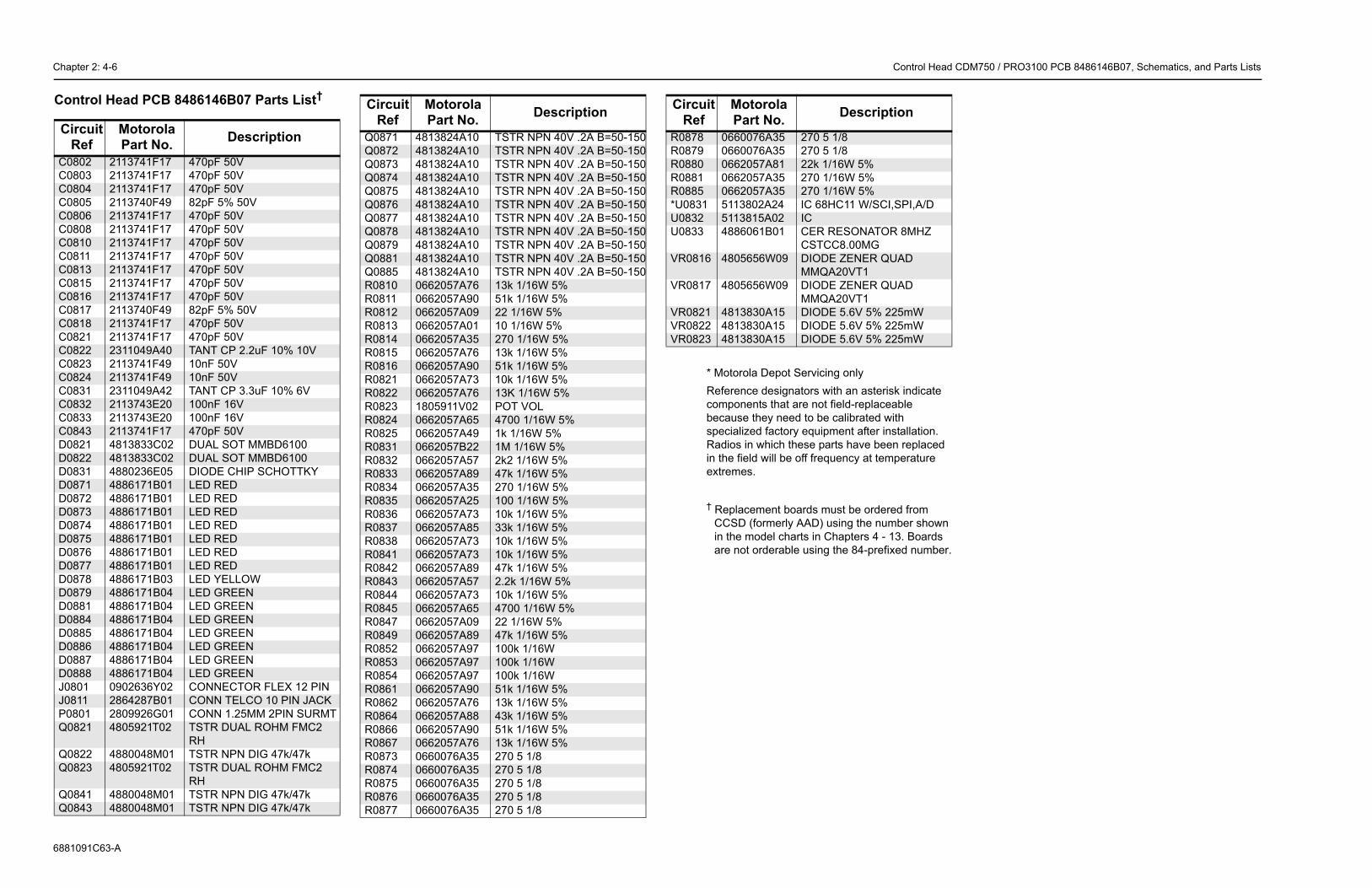
Chapter 2: 4-6 Control Head CDM750 / PRO3100 PCB 8486146B07, Schematics, and Parts Lists
688109
Contr †
onlyh an asterisk indicate eld-replaceable alibrated with ent after installation.
ts have been replaced ency at temperature
st be ordered from ing the number shown apters 4 - 13. Boards he 84-prefixed number.
CircRe
C080C080C080C080C080C080C081C0811C081C081C081C081C081C082C082C082C082C083C083C083C084D082D082D083D087D087D087D087D087D087D087D087D087D088D088D088D088D088D088J0801J0811P0801Q082
Q082Q082
Q084Q084
/8/86W 5%6W 5%6W 5%C11 W/SCI,SPI,A/D
ESONATOR 8MHZ 8.00MG ZENER QUAD 20VT1 ZENER QUAD 20VT1 5.6V 5% 225mW 5.6V 5% 225mW 5.6V 5% 225mW
Description
1C63-A
ol Head PCB 8486146B07 Parts List
* Motorola Depot ServicingReference designators witcomponents that are not fibecause they need to be cspecialized factory equipmRadios in which these parin the field will be off frequextremes.
† Replacement boards muCCSD (formerly AAD) usin the model charts in Chare not orderable using t
uitf
MotorolaPart No. Description
2 2113741F17 470pF 50V3 2113741F17 470pF 50V4 2113741F17 470pF 50V5 2113740F49 82pF 5% 50V6 2113741F17 470pF 50V8 2113741F17 470pF 50V0 2113741F17 470pF 50V
2113741F17 470pF 50V3 2113741F17 470pF 50V5 2113741F17 470pF 50V6 2113741F17 470pF 50V7 2113740F49 82pF 5% 50V 8 2113741F17 470pF 50V1 2113741F17 470pF 50V2 2311049A40 TANT CP 2.2uF 10% 10V3 2113741F49 10nF 50V4 2113741F49 10nF 50V1 2311049A42 TANT CP 3.3uF 10% 6V2 2113743E20 100nF 16V3 2113743E20 100nF 16V3 2113741F17 470pF 50V1 4813833C02 DUAL SOT MMBD61002 4813833C02 DUAL SOT MMBD61001 4880236E05 DIODE CHIP SCHOTTKY1 4886171B01 LED RED2 4886171B01 LED RED3 4886171B01 LED RED4 4886171B01 LED RED5 4886171B01 LED RED6 4886171B01 LED RED7 4886171B01 LED RED8 4886171B03 LED YELLOW9 4886171B04 LED GREEN1 4886171B04 LED GREEN4 4886171B04 LED GREEN5 4886171B04 LED GREEN6 4886171B04 LED GREEN7 4886171B04 LED GREEN8 4886171B04 LED GREEN
0902636Y02 CONNECTOR FLEX 12 PIN2864287B01 CONN TELCO 10 PIN JACK2809926G01 CONN 1.25MM 2PIN SURMT
1 4805921T02 TSTR DUAL ROHM FMC2 RH
2 4880048M01 TSTR NPN DIG 47k/47k3 4805921T02 TSTR DUAL ROHM FMC2
RH1 4880048M01 TSTR NPN DIG 47k/47k3 4880048M01 TSTR NPN DIG 47k/47k
Q0871 4813824A10 TSTR NPN 40V .2A B=50-150Q0872 4813824A10 TSTR NPN 40V .2A B=50-150Q0873 4813824A10 TSTR NPN 40V .2A B=50-150Q0874 4813824A10 TSTR NPN 40V .2A B=50-150Q0875 4813824A10 TSTR NPN 40V .2A B=50-150Q0876 4813824A10 TSTR NPN 40V .2A B=50-150Q0877 4813824A10 TSTR NPN 40V .2A B=50-150Q0878 4813824A10 TSTR NPN 40V .2A B=50-150Q0879 4813824A10 TSTR NPN 40V .2A B=50-150Q0881 4813824A10 TSTR NPN 40V .2A B=50-150Q0885 4813824A10 TSTR NPN 40V .2A B=50-150R0810 0662057A76 13k 1/16W 5%R0811 0662057A90 51k 1/16W 5%R0812 0662057A09 22 1/16W 5%R0813 0662057A01 10 1/16W 5%R0814 0662057A35 270 1/16W 5%R0815 0662057A76 13k 1/16W 5%R0816 0662057A90 51k 1/16W 5%R0821 0662057A73 10k 1/16W 5%R0822 0662057A76 13K 1/16W 5%R0823 1805911V02 POT VOLR0824 0662057A65 4700 1/16W 5%R0825 0662057A49 1k 1/16W 5%R0831 0662057B22 1M 1/16W 5%R0832 0662057A57 2k2 1/16W 5%R0833 0662057A89 47k 1/16W 5%R0834 0662057A35 270 1/16W 5%R0835 0662057A25 100 1/16W 5%R0836 0662057A73 10k 1/16W 5%R0837 0662057A85 33k 1/16W 5%R0838 0662057A73 10k 1/16W 5%R0841 0662057A73 10k 1/16W 5%R0842 0662057A89 47k 1/16W 5%R0843 0662057A57 2.2k 1/16W 5%R0844 0662057A73 10k 1/16W 5%R0845 0662057A65 4700 1/16W 5%R0847 0662057A09 22 1/16W 5%R0849 0662057A89 47k 1/16W 5%R0852 0662057A97 100k 1/16WR0853 0662057A97 100k 1/16WR0854 0662057A97 100k 1/16WR0861 0662057A90 51k 1/16W 5%R0862 0662057A76 13k 1/16W 5%R0864 0662057A88 43k 1/16W 5%R0866 0662057A90 51k 1/16W 5%R0867 0662057A76 13k 1/16W 5%R0873 0660076A35 270 5 1/8R0874 0660076A35 270 5 1/8R0875 0660076A35 270 5 1/8R0876 0660076A35 270 5 1/8R0877 0660076A35 270 5 1/8
CircuitRef
MotorolaPart No. Description
R0878 0660076A35 270 5 1R0879 0660076A35 270 5 1R0880 0662057A81 22k 1/1R0881 0662057A35 270 1/1R0885 0662057A35 270 1/1*U0831 5113802A24 IC 68HU0832 5113815A02 IC U0833 4886061B01 CER R
CSTCCVR0816 4805656W09 DIODE
MMQAVR0817 4805656W09 DIODE
MMQAVR0821 4813830A15 DIODEVR0822 4813830A15 DIODEVR0823 4813830A15 DIODE
CircuitRef
MotorolaPart No.

Control Head CDM1250 / PRO5100 / CDM1550 Series / PRO7100 PCB 8486155B06, Schematics, and Parts Lists Chapter 2: 4-7
6881091C63-A
3 nd Parts Lists
ZWG0130136-A Top Side
ZWG0130137-B Bottom Side
D0
93
7
D0
94
1
D0
94
2
D0
94
5
D0
94
6
D0
95
3D
09
54
D0
95
8
D0
96
7
D0
97
1
D0
97
2
D0
97
5
D0
97
6
D0
98
3D
09
84
D0
98
8
40
80
S0908
S0910
0
0
C0
81
0
C0
811
C0
81
2C
08
13
C0
81
5
C0
81
6
C0
81
7C
08
18
C0
81
9
C0821
C0822
C08230831
32
D0
82
1
D0822
Q0
82
1
Q0822
Q0
82
3
Q0
84
1
Q0843
Q0877
Q0
87
8
Q0
87
9
R0
81
0
R0
811
R0
81
2
R0
81
3
R0
81
4
R0815
R0
81
6
R0
81
7
R0821
R0822
R0824
R0825
R0
84
1
R0
84
3R
08
44
R0
84
549
R0877R0878
TP0831
TP0832
TP0833
TP
08
35
TP0837
TP0838
1
17
14
5 8
U0832 U0
83
5
VR
08
11
VR
08
12
VR
08
16
VR0817
VR
08
21
VR
0822
64
d CDM1250 / PRO5100 / CDM1550 Series / PRO7100 - PCB 8486155B06
.0 Control Head CDM1250 / PRO5100 / CDM1550 Series / PRO7100 PCB 8486155B06, Schematics, a
D0877D0879D0880
D0
93
1D
09
32
D0
93
3D
09
34
D0
93
5D
09
36
D0
93
8
D0
93
9D
09
40
D0
94
3D
09
44
D0
94
7D
09
48
D0
94
9D
09
50
D0
95
1D
09
52
D0
95
5D
09
56
D0
95
7
D0
96
1D
09
62
D0
96
3D
09
64
D0
96
5D
09
66
D0
96
8
D0
96
9D
09
70
D0
97
3D
09
74
D0
97
7D
09
78
D0
97
9D
09
80
D0
98
1D
09
82
D0
98
5D
09
86
D0
98
7
41
H0971
2
3579
8 6 4 10
J0811
4
1
23
5R0823
S0852
S0853
S0854
S0901
S0902
S0903
S0904
S0905
S0906
S0907
S0909
U0834
1 10 320
60 750
1
C0802
C0803
C0804
C0805
C0806
C0807
C0808
C
C08
C0833
C0842
C0
84
3
C0
93
1
C0932
C0
93
3
C0971
C0972
C0973
C0974C0975
C0976 C0977
C0978C0979
C0980C0981
C0982
C0983
C0984
C0985
D0
83
1
12
J0801
12
P0801
1
2
3
4 Q0931 Q0932
1
2
3
4 Q0933
Q0
93
4
R0831
R0832
R0833
R0834
R0
83
5
R0836
R0837
R0838
R0842
R0
84
7
R0848
R08
R0
85
0
R0851
R0852
R0853
R0854
R0855
R0
85
6
R0857
R0858
R0859
R0860
R0861
R0862
R0863
R0
86
4
R0
86
5
R0879
R0901
R0902R0903
R0904
R0905
R0906R0907
R0
90
8 R0909
R0910
R0
93
1R
09
32
R0933
R0
93
4R0935
R0
93
6
R0937R0938
R0
94
1
R0942
R0943
R0944R0945
R0
94
6R0947
R0948
R0972
R0
97
3
R0974
R0975
R0976R0977
R0
97
8
TP0834
TP
08
36
TP0971
TP0972
TP0973
TP0974TP0975
49
33
U0831
3U0833
1 4
58
U0931
128103102
6564
3839
U0971
1
1
1
Control Hea
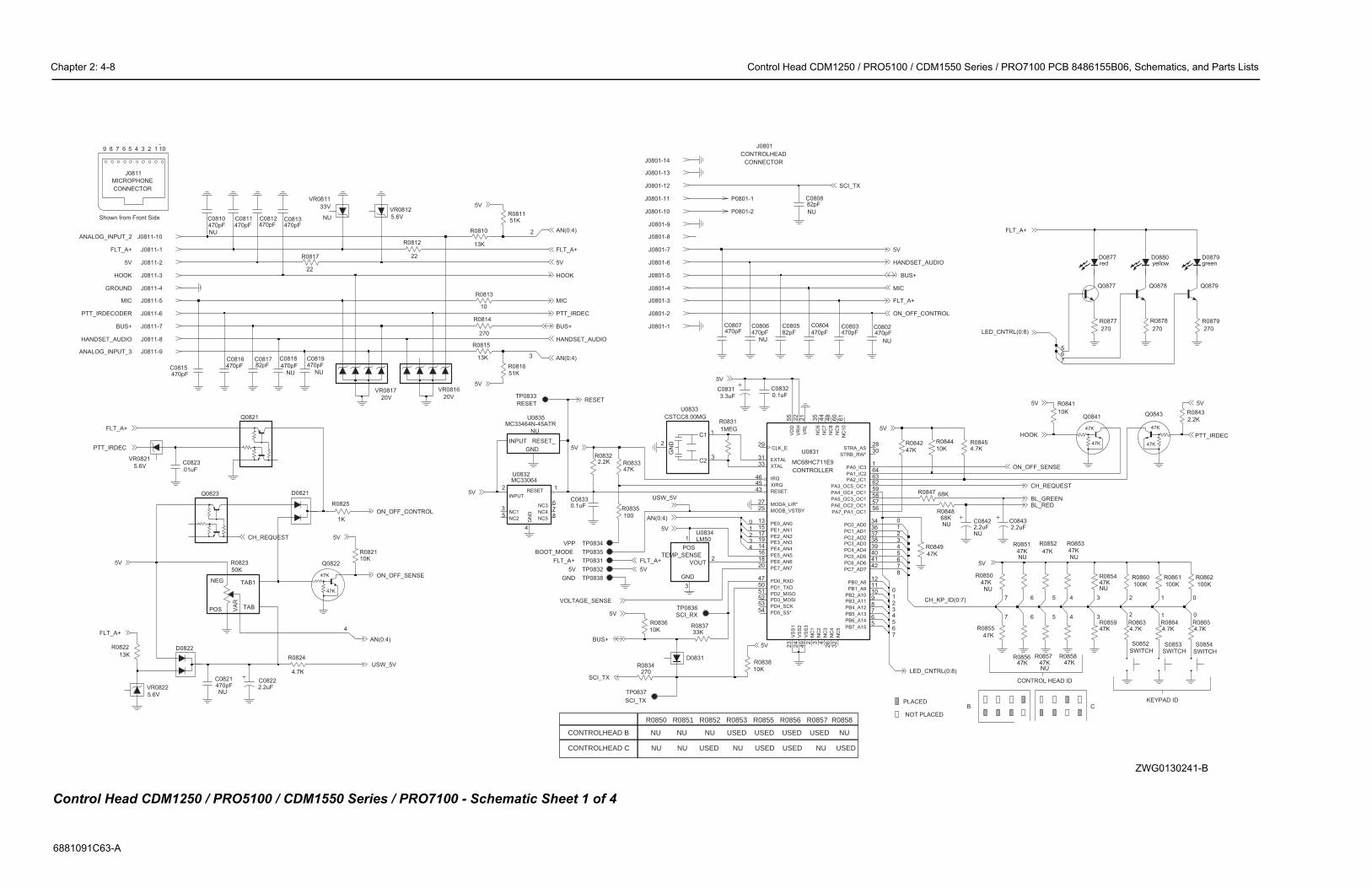
Chapter 2: 4-8 Control Head CDM1250 / PRO5100 / CDM1550 Series / PRO7100 PCB 8486155B06, Schematics, and Parts Lists
688109
NU
USED
0858
47K
47K
47K
47K
P
CKEYPAD ID
B
NOT PLACED
PLACED
H
AN
CONTROL HEAD ID
AN
4.7KR0864
Q0841
6
270
R0877
7
R0852
47K
S0854
SWITCHSWITCHS0853S0852
SWITCH
67
4
8
3
47K
7
NU
R0851
greenD0879
R0857
1
NU47K
D0880yellow
47KNU
R0854
47KR0859
10K
R0841
2.2K
R0843
R084868KNU
5
0
R0879
270
R0878
270
R0844
10K
R08654.7K
100K
R0860
47KNU
R0853
5
7
0
4
4.7KR0845
C0842
NU2.2uF
Q0879Q0878
redD0877
Q0877
3R08634.7K
NU
R0850
47K
R085647K
2
28STRA_AS
30STRB_RW*
36
PC2_AD237
PC3_AD338
PC4_AD439
PC5_AD540
PC6_AD641
PC7_AD742
11
PB2_A1010
PB3_A119
PB4_A128
PB5_A137
PB6_A146
PB7_A155
PC0_AD034
PC1_AD1
PA1_IC263
PA2_IC162
3_OC5_OC159
4_OC4_OC158
5_OC3_OC157
6_OC2_OC156
A7_PA1_OC1
PB0_A812
PB1_A9
32
NC
56
0N
C9
1PA0_IC3
64
61
NC
10
4
1
2.2uFC0843
2
0
47K
R0842
3
47K
R0849
47K
R08557
470pFC0803
1
R0847 68K
47KR0858
Q0843
6
6
5
1
0
5
3 2
NU
470pFC0802
2
100K
R0862
4
100K
R0861
56
BL_REDBL_GREEN
5V
5V
PTT_IRDECHOOK
5V
CH_REQUEST
ON_OFF_SENSE
SCI_TX
5V
HANDSET_AUDIO
BUS+
MIC
FLT_A+
ON_OFF_CONTROL
FLT_A+
LED_CNTRL(0:8)
LED_CNTRL(0:8)
CH_KP_ID(0:7)
5V
Contr
ZWG0130241-B
1C63-A
CONTROLHEAD B NU NU NU USED USED USED USED
CONTROLHEAD C NU NU USED NU USED USED NU
R0850 R0851 R0852 R0853 R0855 R0856 R0857 R
47K
47K
MIC
TT_IRDECODER
BUS+
CONTROLLER
VPP
ANDSET_AUDIO
ALOG_INPUT_3
5V
BOOT_MODE
SCI_RX
SCI_TX
FLT_A+
RESET
TEMP_SENSE
5V
GND
HOOK
CONTROLHEAD
CONNECTOR
GROUND
ALOG_INPUT_2
FLT_A+
J0801
J0801-8
270
R0814
R0815
13K
R0810
13K
J0801-5
0
R083347K
R08322.2K
R083733K
J0811-8
GND
INPUT RESET_
NU
U0835MC33464N-45ATR
J0801-3
J0801-10
J0801-13
J0811-9
J0801-14
J0811-10
10
R0813
J0801-7
5.6V
VR0822
D0831
Q0821
U0833
CSTCC8.00MG
C1 1
C23
GN
D2
J0811-6
J0801-4
470pFC0812
22
R0817
1
51K
R0816
J0811-7
Q0823
R0831
TAB1
VA
R
1MEG
R0823
50K
NEG
POS TAB
J0801-12
J0801-9
C0831
NC4
NC58
1RESET
3.3uF
MC33064
4G
ND
2
INPUT
3NC1
5NC2
6NC3
7
U0832
R0812
22
D0822
J0811-5
3
J0801-11
Q0822
R081151K
TP0833
1K
R0825
470pF
C0804
13K
TP0836
R0822
TP0834
470pFC0821
4
NU
VR0812
5.6V
4
82pFC0805
VD
D2
2V
RH
21
VR
L
23
VS
S1
24
VS
S2
49
VS
S3
45 XIRQ
33 XTAL
19
PE4_AN414
PE5_AN516
PE6_AN618
PE7_AN720
RESET43
55
50
PD2_MISO51
PD3_MOSI52
PD4_SCK53
PD5_SS*54
PE0_AN013
PE1_AN115
PE2_AN217
PE3_AN3
PD0_RXD47
PD1_TXD
PA
PA
PA
PA
P
NC
32
6N
C4
35
NC
64
4N
C7
48
NC
8
CLK_E
31 EXTAL
46 IRQ
27 MODA_LIR*25 MODB_VSTBY
2N
C1
3N
C2
4
MC68HC711E9
U0831
29
J0811-4
J0811-3
J0811-2
C08222.2uF
R0838
10K
R0836
10K
VR0816
20VVR0817
20V 0.1uFC0832
C08330.1uF
VR0821
5.6V
C0819C0816
NU
470pF470pF 82pFC0817
TP0831
P0801-2
P0801-1
TP0835
C0806470pF
NU
470pFC0813
C0815470pF
C0807470pF
VOUT
D0821
U0834LM50
3
GND
1
POS
2R082110K
3
J0801-1
270R0834
2
J0801-6
R0824
4.7K
470pFC0810
VR0811
33V
NU
C0811 NU
470pF
470pF
C0818
NU
TP0837
TP0832
TP0838
100
R0835
J0801-2
J0811-1
82pFC0808
NU
2
C0823
.01uF
5V
5V
5V
BUS+5V
RESET
5V
HOOK
MIC
5V
FLT_A+
5V
SCI_TX
5V
VOLTAGE_SENSE
HANDSET_AUDIO
PTT_IRDEC
BUS+
AN(0:4)
AN(0:4)
USW_5V
FLT_A+5V
CH_REQUEST
ON_OFF_CONTROL
5V
5V
ON_OFF_SENSE
PTT_IRDEC
FLT_A+
5V
AN(0:4)
USW_5V
FLT_A+
AN(0:4)
10
GM300
789
MICROPHONE
CONNECTOR
J0811
WARIS
1456 23
Shown from Front Side
ol Head CDM1250 / PRO5100 / CDM1550 Series / PRO7100 - Schematic Sheet 1 of 4

Control Head CDM1250 / PRO5100 / CDM1550 Series / PRO7100 PCB 8486155B06, Schematics, and Parts Lists Chapter 2: 4-9
6881091C63-A
P6
7P7
8P8
1P1
2P2
3P3
4P4
5P5
6
P5
6P6
7P7
8P8
SWITCHS0901
1P1
2P2
3 P3
4P4
5
4P4
5P5
6P6
7P7
8P8
SWITCHS0905
1P1
2P2
3P3
3P3
4P4
5P5
6P6
7P7
8P8
SWITCHS0902
SWITCHS0910
1P1
2P2
2P2
3P3
4P4
5P5
6P6
7P7
8P8
P8
SWITCHS0908
1P1
1P1
2P2
3P3
4P4
5P5
6P6
7P7
8
7P7
8P8
SWITCHS0906
1P1
2P2
3P3
4P4
5P5
6P6
SWITCHS0903
P4
5P5
6P6
7P7
8P8
1P1
2P2
3P3
4
P3
4P4
5P5
6P6
7P7
8P8
SWITCHS0909
1P1
2P2
3
P2
3P3
4P4
5P5
6P6
7P7
8P8
SWITCHS0907
SWITCHS0904
1P1
2
COL3 COL2
ROW1
ROW2
ROW3
ROW4
COL4
ZWG0130242-A
M1250 / PRO5100 / CDM1550 Series / PRO7100 - Schematic Sheet 2 of 4
P4
SW0906 SW0904
SW0903 SW0901
SW0909 SW0910
SW0908SW0907
SW0902
SW0905
KEYPAD C LAYOUT
SW0908SW0905
SW0902
KEYPAD B LAYOUT
P3P1
P2 P4
SW0906 SW0910
SW0903
P1
P2
P3
43K
0
1
R090943K
130K
R0904
130K
NU
R0910
NU
R0905
R090651K
R090151K
R090822K
R090322K
R090213K
R090713K
ZWG0130242-A
COL2
COL1
ROW2
ROW1
ROW3 COL3
5V
ROW5
ROW4
COL5
COL4
AN(0:4)
Control Head CD

Chapter 2: 4-10 Control Head CDM1250 / PRO5100 / CDM1550 Series / PRO7100 PCB 8486155B06, Schematics, and Parts Lists
688109
BACKLIGHT RED
100K
NU
R0934
10K
R0935
NUD0951
NUD0947
NUD0943
NUD0932
NUD0931
10
R0938R0937
10NUNU
C0932
0.1uF
R0936
10K
NUD0949
932
MC33072
U0931-1
2
31
8
4
U
D0942NU
NUD0941
NUD0940
NUD0938
NUD0937
NUD0958
NUD0957
NUD0956
D0954
D0953
NU
D0952
NU
D0950
NU
NU
NUD0939
NUD0935
D0933
NUD0934
NU
D0936NU
D0955
D0948
NU
D0946
NU
NU
D0944
NUD0945
FL
FL
BL_GR
NU
Contr ZWG0130243-A
1C63-A
BACKLIGHT GREEN
NUQ0931
D0980
D0979
D0978
R0946
D0977
R0945
10K
33K
10K
R0942
10K
R0941
D0972
R0944
10
100K
R0947 R0948
4
10
U0931-2
MC33072
6
5
78
Q0933
D0987
D0986
D0985
D0984
D0969
D0967
D0966
D0964
D0965
NU
NUD0963
D0970
NUD0962
D0971
Q0934
4.7K
R0943
C0931
0.1uF
R0932
NU
33K
NU
R0931
10K
Q0
N
D0975
D0976
D0974
D0973
0.1uF
C0933
D0968 D0988
4.7KNU
R0933
NUD0961
D0983
D0982
D0981FLT_A+
T_A+
T_A+
EEN BL_RED
FLT_A+
ol Head CDM1250 / PRO5100 / CDM1550 Series / PRO7100 - Schematic Sheet 3 of 4
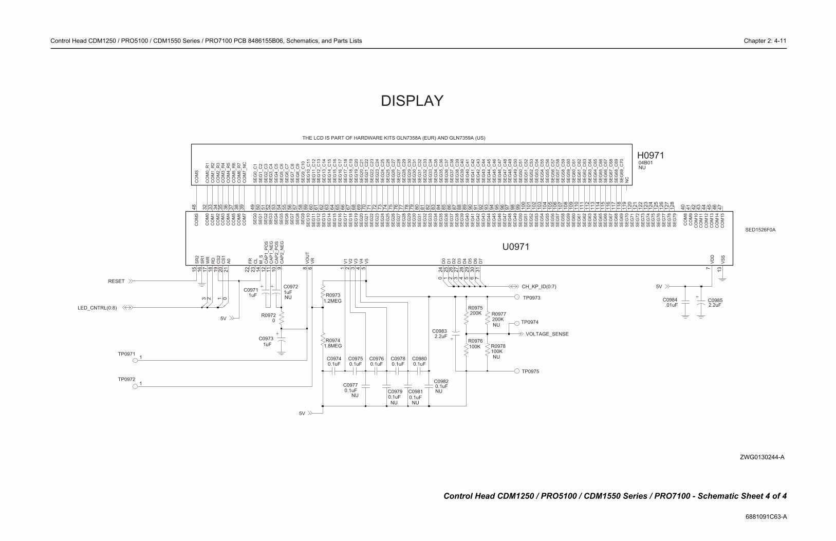
Control Head CDM1250 / PRO5100 / CDM1550 Series / PRO7100 PCB 8486155B06, Schematics, and Parts Lists Chapter 2: 4-11
6881091C63-A
2.2uFC0985
.01uFC0984
04B01
H0971
SE
G6
9_
C7
0
SE
G6
1_
C6
2
SE
G6
2_
C6
3
SE
G6
3_
C6
4
SE
G6
4_
C6
5
SE
G6
5_
C6
6S
EG
66
_C
67
SE
G6
7_
C6
8
SE
G6
8_
C6
9
SE
G5
4_
C5
5
SE
G5
5_
C5
6
SE
G5
6_
C5
7S
EG
57
_C
58
SE
G5
8_
C5
9
SE
G5
9_
C6
0
SE
G6
0_
C6
1
SE
G4
8_
C4
9
SE
G4
9_
C5
0
SE
G5
0_
C5
1
SE
G5
1_
C5
2
SE
G5
2_
C5
3
SE
G5
3_
C5
4
NC
7
13
NU
12
11
22
12
31
24
12
51
26
12
71
28
11
41
15
11
61
17
11
81
19
12
0
10
71
08
10
91
10
111
11
21
13
99
10
01
01
10
21
03
10
41
05
10
6
97
98
40
41
44
45
46
47
42
43
SED1526F0A
0971
VD
D
VS
S
SE
G7
2
SE
G7
3
SE
G7
4S
EG
75
SE
G7
6
SE
G7
7
SE
G7
8
SE
G7
9
SE
G6
5S
EG
66
SE
G6
7
SE
G6
8
SE
G6
9
SE
G7
0
SE
G7
1
SE
G5
8
SE
G5
9
SE
G6
0
SE
G6
1
SE
G6
2
SE
G6
3
SE
G6
4
SE
G5
0
SE
G5
1
SE
G5
2
SE
G5
3
SE
G5
4
SE
G5
5
SE
G5
6S
EG
57
SE
G4
8
SE
G4
9
CO
M8
CO
M9
CO
M1
2
CO
M1
3
CO
M1
4
CO
M1
5
CO
M1
0C
OM
11
TP0974
TP0973
TP0975
5VCH_KP_ID(0:7)
VOLTAGE_SENSE
ZWG0130244-A
M1250 / PRO5100 / CDM1550 Series / PRO7100 - Schematic Sheet 4 of 4
THE LCD IS PART OF HARDWARE KITS GLN7358A (EUR) AND GLN7359A (US)
DISPLAY
R09741.8MEG
R0973
1.2MEG
R0972
C0972
0
NU1uF
1uFC0971
1uF
C0973
0.1uFC0980
0.1uFC0976C0975
0.1uFC09740.1uF
NU
C09820.1uF
0.1uF
C0981C09790.1uF
NU
0.1uFC0977
NU
12
NU
3 4 5 6 7
0
100KR0978
200KR0977
NU
NU
1
100K
R0976
0
SE
G6
_C
7
SE
G7
_C
8
SE
G8
_C
9
SE
G9
_C
10
SE
G5
_C
6
SE
G4
7_
C4
8
SE
G4
_C
5
SE
G3
_C
4
SE
G4
0_
C4
1
SE
G4
1_
C4
2
SE
G4
2_
C4
3
SE
G4
3_
C4
4
SE
G4
4_
C4
5
SE
G4
5_
C4
6
SE
G4
6_
C4
7
SE
G3
2_
C3
3
SE
G3
3_
C3
4
SE
G3
4_
C3
5
SE
G3
5_
C3
6
SE
G3
6_
C3
7
SE
G3
7_
C3
8
SE
G3
8_
C3
9S
EG
39
_C
40
SE
G2
5_
C2
6
SE
G2
6_
C2
7
SE
G2
7_
C2
8
SE
G2
8_
C2
9
SE
G2
9_
C3
0
SE
G2
_C
3
SE
G3
0_
C3
1
SE
G3
1_
C3
2
SE
G1
8_
C1
9
SE
G1
9_
C2
0
SE
G1
_C
2
SE
G2
0_
C2
1S
EG
21
_C
22
SE
G2
2_
C2
3
SE
G2
3_
C2
4
SE
G2
4_
C2
5
SE
G1
0_
C1
1
SE
G1
1_
C1
2S
EG
12
_C
13
SE
G1
3_
C1
4
SE
G1
4_
C1
5
SE
G1
5_
C1
6
SE
G1
6_
C1
7
SE
G1
7_
C1
8
CO
M3
_R
4
CO
M4
_R
5
CO
M5
_R
6
CO
M6
_R
7
CO
M7
_N
C
CO
MS
SE
G0
_C
1
CO
M0
_R
1
CO
M1
_R
2
CO
M2
_R
3
58 6
17
57
58
16
15 1 2 3 4
56
55
92
93
94
95
96
54
85
86
87
88
53
89
90
91
78
52
79
80
81
82
83
84
70
71
72
73
74
75
76
77
63
64
65
66
67
68
51
69
14
18
49
50
59
60
61
62
25
26
27
28
29
30
31
22
38
39
48
20
19
24
34
35
36
37
12 9
10
23
32
33
U
21
11
V5
VO
UT
VR
WR
SE
G8
SE
G9
SR
1
SR
2
V1
V2
V3
V4
SE
G7
SE
G6
SE
G4
3
SE
G4
4
SE
G4
5
SE
G4
6
SE
G4
7
SE
G5
SE
G3
6
SE
G3
7
SE
G3
8S
EG
39
SE
G4
SE
G4
0
SE
G4
1
SE
G4
2
SE
G2
9
SE
G3
SE
G3
0
SE
G3
1
SE
G3
2
SE
G3
3
SE
G3
4
SE
G3
5
SE
G2
1
SE
G2
2
SE
G2
3
SE
G2
4
SE
G2
5
SE
G2
6
SE
G2
7
SE
G2
8
SE
G1
4
SE
G1
5
SE
G1
6
SE
G1
7
SE
G1
8
SE
G1
9
SE
G2
SE
G2
0
M_
S
RD
SE
G0
SE
G1
SE
G1
0
SE
G1
1S
EG
12
SE
G1
3
D1
D2
D3
D4
D5
D6
D7
FR
CO
M6
CO
M7
CO
MS
CS
1C
S2
D0
CO
M2
CO
M3
CO
M4
CO
M5
CA
P1
_P
OS
CA
P2
_N
EG
CA
P2
_P
OS
CL
CO
M0
CO
M1
A0
CA
P1
_N
EG
C09780.1uF
3
1
1
TP0972
TP0971
2.2uFC0983
200KR0975
5V
RESET
LED_CNTRL(0:8)
5V
2
Control Head CD
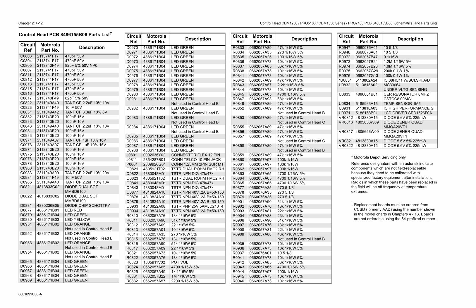
Chapter 2: 4-12 Control Head CDM1250 / PRO5100 / CDM1550 Series / PRO7100 PCB 8486155B06, Schematics, and Parts Lists
688109
Contr †
* Motorola Depot Servicing onlyReference designators with an asterisk indicate components which are not field-replaceable because they need to be calibrated with specialized factory equipment after installation. Radios in which these parts have been replaced in the field will be off frequency at temperature extremes.
† Replacement boards must be ordered from CCSD (formerly AAD) using the number shown in the model charts in Chapters 4 - 13. Boards are not orderable using the 84-prefixed number.
CircuRe
C080C080C080C080C0811C081C081C081C081C081C082C082C083C083C083C084C093C093C097C097C097C097C097C097C098C098C098C098D082
D082
D083D087D087D088D095
D095
D095
D095
D096D096D096D096D096
6W 5%6W 5%6W 5%6W 5%6W 5%6W 5%6W 5%6W 5%6W 5%6W 5%16W 5%6W 5%6W 5%6W 5%d in Control Head B6W 5%d in Control Head C6W 5%6W 5%6W 5%d in Control Head C6W 5%d in Control Head B6W 5%16W16W16W16W 5%16W 5%16W 5%/8/8/86W 5%6W 5%6W 5%6W 5%6W 5%6W 5%6W 5%6W 5%d in Control Head B6W 5%6W 5%
6W 5%6W 5%16W 5%16W6W 5%6W 5%
Description
R0947 0660076A01 10 5 1/8R0948 0660076A01 10 5 1/8R0972 0662057B47 0 1/16WR0973 0662057B24 1.2M 1/16W 5%R0974 0662057B28 1.8M 1/16W 5%R0975 0662057G29 200k 0.1W 1%R0976 0662057G13 100k 0.1W 1%*U0831 5113802A24 IC 68HC11 W/SCI,SPI,A/DU0832 5113815A02 MC33064
UNDER VLTG SENSINGU0833 4886061B01 CER RESONATOR 8MHZ
CSTCC8.00MGU0834 5185963A15 TEMP SENSOR 1M5U0931 5113818A03 IC HIGH PERFORMANCE SIU0971 5186158B01 LCD DRIVER SED1526F0AVR0812 4813830A15 DIODE 5.6V 5% 225mWVR0816 4805656W09 DIODE ZENER QUAD
MMQA20VT1VR0817 4805656W09 DIODE ZENER QUAD
MMQA20VT1VR0821 4813830A15 DIODE 5.6V 5% 225mWVR0822 4813830A15 DIODE 5.6V 5% 225mW
Circuit Ref
Motorola Part No. Description
1C63-A
ol Head PCB 8486155B06 Parts List
it f
Motorola Part No. Description
3 2113741F17 470pF 50V4 2113741F17 470pF 50V5 2113740F49 82pF 5% 50V NP07 2113741F17 470pF 50V
2113741F17 470pF 50V2 2113741F17 470pF 50V3 2113741F17 470pF 50V5 2113741F17 470pF 50V6 2113741F17 470pF 50V7 2113740F49 82pF 5% 50V2 2311049A40 TANT CP 2.2uF 10% 10V3 2113741F49 10nF 50V1 2311049A42 TANT CP 3.3uF 10% 6V2 2113743E20 100nF 16V3 2113743E20 100nF 16V3 2311049A40 TANT CP 2.2uF 10% 10V1 2113743E20 100nF 16V3 2113743E20 100nF 16V1 2311049A07 TANT CP 1uF 10% 16V3 2311049A07 TANT CP 1uF 10% 16V4 2113743E20 100nF 16V5 2113743E20 100nF 16V6 2113743E20 100nF 16V8 2113743E20 100nF 16V0 2113743E20 100nF 16V3 2311049A09 TANT CP 2.2uF 10% 20V4 2113741F49 10nF 50V5 2311049A40 TANT CP 2.2uF 10% 10V1 4813833C02 DIODE DUAL SOT
MMBD61002 4813833C02 DIODE DUAL SOT
MMBD61001 4880236E05 DIODE CHIP SCHOTTKY7 4886171B01 LED RED9 4886171B04 LED GREEN0 4886171B03 LED YELLOW1 4886171B02 LED ORANGE
Not used in Control Head B2 4886171B02 LED ORANGE
Not used in Control Head B3 4886171B02 LED ORANGE
Not used in Control Head B4 4886171B02 LED ORANGE
Not used in Control Head B5 4886171B04 LED GREEN6 4886171B04 LED GREEN7 4886171B04 LED GREEN8 4886171B04 LED GREEN9 4886171B04 LED GREEN
D0970 4886171B04 LED GREEND0971 4886171B04 LED GREEND0972 4886171B04 LED GREEND0973 4886171B04 LED GREEND0974 4886171B04 LED GREEND0975 4886171B04 LED GREEND0976 4886171B04 LED GREEND0977 4886171B04 LED GREEND0978 4886171B04 LED GREEND0979 4886171B04 LED GREEND0980 4886171B04 LED GREEND0981 4886171B04 LED GREEN
Not used in Control Head BD0982 4886171B04 LED GREEN
Not used in Control Head BD0983 4886171B04 LED GREEN
Not used in Control Head BD0984 4886171B04 LED GREEN
Not used in Control Head BD0985 4886171B04 LED GREEND0986 4886171B04 LED GREEND0987 4886171B04 LED GREEND0988 4886171B04 LED GREENJ0801 0902636Y02 CONNECTOR FLEX 12 PINJ0811 2864287B01 CONN TELCO 10 PIN JACKP0801 2809926G01 CONN 1.25MM 2PIN SUR MTQ0821 4805921T02 TSTR DUAL ROHM FMC2 RHQ0822 4880048M01 TSTR NPN DIG 47k/47kQ0823 4805921T02 TSTR DUAL ROHM FMC2 RHQ0841 4880048M01 TSTR NPN DIG 47k/47kQ0843 4880048M01 TSTR NPN DIG 47k/47kQ0877 4813824A10 TSTR NPN 40V .2A B=50-150Q0878 4813824A10 TSTR NPN 40V .2A B=50-150Q0879 4813824A10 TSTR NPN 40V .2A B=50-150Q0933 4813822A08 TSTR PNP 25V 5AMJD210T4Q0934 4813824A10 TSTR NPN 40V .2A B=50-150R0810 0662057A76 13k 1/16W 5%R0811 0662057A90 51k 1/16W 5%R0812 0662057A09 22 1/16W 5%R0813 0662057A01 10 1/16W 5%R0814 0662057A35 270 1/16W 5%R0815 0662057A76 13k 1/16W 5%R0816 0662057A90 51k 1/16W 5%R0817 0662057A09 22 1/16W 5%R0821 0662057A73 10k 1/16W 5%R0822 0662057A76 13k 1/16W 5%R0823 1805911V02 POT VOLR0824 0662057A65 4700 1/16W 5%R0825 0662057A49 1k 1/16W 5%R0831 0662057B22 1M 1/16W 5%R0832 0662057A57 2200 1/16W 5%
Circuit Ref
Motorola Part No. Description
R0833 0662057A89 47k 1/1R0834 0662057A35 270 1/1R0835 0662057A25 100 1/1R0836 0662057A73 10k 1/1R0837 0662057A85 33k 1/1R0838 0662057A73 10k 1/1R0841 0662057A73 10k 1/1R0842 0662057A89 47k 1/1R0843 0662057A57 2.2k 1/1R0844 0662057A73 10k 1/1R0845 0662057A65 4700 1/R0847 0662057A93 68k 1/1R0849 0662057A89 47k 1/1R0852 0662057A89 47k 1/1
Not useR0853 0662057A89 47k 1/1
Not useR0855 0662057A89 47k 1/1R0856 0662057A89 47k 1/1R0857 0662057A89 47k 1/1
Not useR0858 0662057A89 47k 1/1
Not useR0859 0662057A89 47k 1/1R0860 0662057A97 100k 1/R0861 0662057A97 100k 1/R0862 0662057A97 100k 1/R0863 0662057A65 4700 1/R0864 0662057A65 4700 1/R0865 0662057A65 4700 1/R0877 0660076A35 270 5 1R0878 0660076A35 270 5 1R0879 0660076A35 270 5 1R0901 0662057A90 51k 1/1R0902 0662057A76 13k 1/1R0903 0662057A81 22k 1/1R0904 0662057A88 43k 1/1R0906 0662057A90 51k 1/1R0907 0662057A76 13k 1/1R0908 0662057A81 22k 1/1R0909 0662057A88 43k 1/1
Not useR0935 0662057A73 10k 1/1R0936 0662057A73 10k 1/1R0937 0660076A01 10 5 1/8R0941 0662057A73 10k 1/1R0942 0662057A85 33k 1/1R0943 0662057A65 4700 1/R0944 0662057A97 100k 1/R0945 0662057A73 10k 1/1R0946 0662057A73 10k 1/1
Circuit Ref
Motorola Part No.

Chapter 3: i
Chapter 3: Controller Service MaintainabilityTable of Contents
Section 1 Theory of Operation
1.0 Controller Circuits .............................................................................................3:1-11.1 Overview......................................................................................................3:1-11.2 General........................................................................................................3:1-11.3 Radio Power Distribution .............................................................................3:1-21.4 Electronic ON/OFF ......................................................................................3:1-41.5 Emergency ..................................................................................................3:1-41.6 Mechanical ON/OFF....................................................................................3:1-51.7 Ignition .........................................................................................................3:1-51.8 Microprocessor Clock Synthesizer ..............................................................3:1-51.9 Serial Peripheral Interface (SPI)..................................................................3:1-61.10 SBEP Serial Interface..................................................................................3:1-71.11 General Purpose Input/Output.....................................................................3:1-71.12 Normal Microprocessor Operation...............................................................3:1-81.13 FLASH Electronically Erasable Programmable Memory
(FLASH EEPROM) ......................................................................................3:1-91.14 Electrically Erasable Programmable Memory (EEPROM)...........................3:1-91.15 Static Random Access Memory (SRAM)...................................................3:1-10
2.0 Controller Board Audio and Signaling Circuits................................................3:1-102.1 Audio Signaling Filter IC with Compander (ASFIC CMP)..........................3:1-102.2 Transmit Audio Circuits .............................................................................3:1-112.3 Transmit Signaling Circuits........................................................................3:1-132.4 Receive Audio Circuits ..............................................................................3:1-152.5 Receive Signaling Circuits.........................................................................3:1-182.6 Voice Storage (Optional) ...........................................................................3:1-19
Section 2 Troubleshooting Charts
1.0 Troubleshooting Flow Chart for Controller ........................................................3:2-1
Section 3 Controller Schematics and Parts Lists
1.0 Allocation of Schematics and Circuit Boards ....................................................3:3-11.1 Controller Circuits ........................................................................................3:3-11.2 Voice Storage Facility..................................................................................3:3-1
2.0 Controller T2 Schematics and Parts Lists.........................................................3:3-33.0 Controller T5 Schematics and Parts Lists.......................................................3:3-104.0 Controller T6/T7/T9 Schematics and Parts Lists ............................................3:3-18
6881091C63-A

Chapter 3: ii
5.0 Controller T11 Schematics and Parts Lists.....................................................3:3-316.0 Controller T12 Schematics and Parts Lists.....................................................3:3-37
6881091C63-A
Chapter 3: 1-1
Section 1THEORY OF OPERATION
1.0 Controller Circuits
1.1 Overview
This section provides a detailed theory of operation for the radio and its components. The main radio is a single-board design, consisting of the transmitter, receiver, and controller circuits. The main board is designed to accept one option board. The option board may provide functions such as secure voice/data, voice storage, or signaling decoder.
A control head is either mounted directly or connected by an extension cable. The control head contains LED indicators, a microphone connector, buttons, and—depending on the radio type—a display and a speaker. These provide the user with interface control over the various features of the radio.
If no control head is mounted directly on the front of the radio, an expansion board containing circuitry for special applications can be mounted on the front of the radio. An additional control head can be connected by an extension cable.
In addition to the power cable and antenna cable, an accessory cable can be attached to a connector on the rear of the radio. The accessory cable enables you to connect accessories to the radio, such as an external speaker, emergency switch, foot-operated PTT, and ignition sensing, etc.
1.2 General
The radio controller consists of three main subsections:
• digital control• audio processing• voltage regulation
The digital control section of the radio is based upon an open architecture controller configuration. It consists of a microprocessor, support memory, support logic, signal MUX ICs, the On/Off circuit, and general purpose Input/Output circuitry.
The controller uses the Motorola 68HC11FL0 microprocessor (U0101). The controller also has three external memory devices. These devices consist of a 32KByte SRAM (U0122), a 512KByte FLASH EEPROM (U0121), and a 16KByte EEPROM (U0111).
NOTE From this point on, the 68HC11FL0 microprocessor is referred to as “µP”. References to acontrol head indicate the control heads with display.
6881091C63-A

Chapter 3: 1-2 Controller Circuits
Figure 3-1 Controller Block Diagram
1.3 Radio Power Distribution
The DC power distribution throughout the radio board is shown in Figure 3-2. Voltage regulation for the controller is provided by 4 separate devices; U0651 (MC78M05) 5V, U0641 (LM2941) 9.3V, U0611 (LM2941) SWB+ limited to 16.5V and VSTBY 5V (a combination of R0621 and VR0621). An additional 5V regulator is located on the RF section.
The DC voltage applied to connector J0601 supplies power directly to the electronic on/off control, RF power amplifier, 16.5V limiter, 9.3V regulator, Audio PA and 5.6V stabilization circuit. The 9.3V regulator (U0641) supplies power to the 5V regulator (U0651) and the 6V voltage divider Q0681.
Regulator U0641 is used to generate the 9.3 volts required by some audio circuits, the RF circuitry and power control circuitry. Input and output capacitors (C0641 and C0644 / C0645) are used to reduce high frequency noise. R0642 / R0643 set the output voltage of the regulator. If the voltage at pin 1 is greater than 1.3 volts the regulator output decreases and if the voltage is less than 1.3 volts the regulator output increases. This regulator output is electronically enabled by a 0 volt signal on pin 2. Q0661, Q0641 and R0641 are used to disable the regulator when the radio is turned off.
Voltage regulation providing 5V for the digital circuitry is done by U0651. Operating voltage is from the regulated 9.3V supply. Input and output capacitors (C0651 / C0652 and C0654 / C0655) are used to reduce high frequency noise and provide proper operation during battery transients. Voltage sense device U0652 or alternatively U0653 provides a reset output that goes to 0 volts if the regulator output goes below 4.5 volts. This is used to reset the controller to prevent improper operation. Diode D0651 prevents discharge of C0652 by negative spikes on the 9.3V voltage.
ExternalMicrophone
InternalMicrophone
ExternalSpeaker
InternalSpeaker
SCI to
Control Head
Audio PA
Audio/Signaling Architecture
To SynthesizerModOut
16.8 MHzReference Clockfrom Synthesizer
Recovered Audio
To RF Section SPI
DigitalArchitecture
µP Clock
5VRegulator (5VD)
RAM
EEPROM
FLASH
HC11FL0
ASFIC_CMP
Accessory &
5Vfrom SynthesizerSection (5V_RF)
Connector
6881091C63-A

Controller Circuits Chapter 3: 1-3
Transistor Q0681 and resistors R0681 / R0682 divide the regulated 9.3V down to about 6 volts. This voltage supplies the 5V regulator, located on the RF section. By reducing the supply voltage of the regulator, the power dissipation is divided between the RF section and the controller section.
The voltage VSTBY, which is derived directly from the supply voltage by components R0621 and VR0621, is used to buffer the internal RAM. C0622 allows the battery voltage to be disconnected for a couple of seconds without losing RAM parameters. Dual diode D0621 prevents radio circuitry from discharging this capacitor. When the supply voltage is applied to the radio, C0622 is charged via R0621 and D0621. To avoid the µP entering the wrong mode when the radio is switched on while the voltage across C0622 is still too low, the regulated 5V supply charges C0622 via diode D0621.
Figure 3-2 DC Power Distribution Block Diagram
The voltage INT SW B+ from switching transistor Q0661 provides power to the circuit controlling the audio PA output. The voltage INT SW B+ voltage is monitored by the µP through voltage divider R0671 / R0672 and line BATTERY VOLTAGE. Diode VR0671 limits the divided voltage to 5.6V to protect the µP.
Regulator U0611 is used to generate the voltage for the switched supply voltage output (SWB+) at the accessory connector J0501 pin 13. U0611 is configured to operate as a switch with voltage and current limit. R0611 / R0612 set the maximum output voltage to 16.5 volts. This limitation is only active at high supply voltage levels. The regulator output is electronically enabled by a 0 volt signal on pin 2. Q0661, Q0641 and R0641 are used to disable the regulator when the radio is turned off. Input and output capacitors (C0603 and C0611 / C0612) are used to reduce high frequency noise.
Diode VR0601 acts as protection against transients and wrong polarity of the supply voltage.
Fuse F0401 prevents damage of the board in case the FLT A+ line is shorted at the control head connector.
VCOBIC FRACTN
VSTBY
5V_RF
9.3V
FLT_A+
5VD
SWB+
Option Board 40 Pin Connector
PA, Driver Antenna Switch
Control Head12 Pin Connector
Accessories20 Pin Connector
J0601 13.2V
PASUPVLTG
FLT_A+
16.5VLimiter
ON / OFFControl
ASFIC_CMP5.6V
IgnitionEmergencyON/OFF
9.3VRegulator
Audio PA
6VRegulator
5VRegulator
5VD
5VRegulator 5V/
VDDA
MCU µP, RAM,
FLASH & EEPROM
PCIC, TX Amp
Temp Sense
RX RF AmpIF Amp
F040
1
6881091C63-A
Chapter 3: 1-4 Controller Circuits
1.4 Electronic ON/OFF
The radio has circuitry which allows radio software and/or external triggers to turn the radio on or off without direct user action (for example, automatic turn on when ignition is sensed and off when ignition is off).
Q0661 is used to provide INT SW B+ to the various radio circuits and to enable the voltage regulators via transistor Q0641. Q0661 contains an pnp and an npn transistor and acts as an electronic on/off switch. The switch is on when the collector of the npn transistor within Q0661 is low. When the radio is off the collector is at supply voltage level. This effectively prevents current flow from emitter to collector of the pnp transistor. When the radio is turned on the voltage at the base of the npn transistor is pulled high and the pnp transistor switches on (saturation). With voltage INT SWB+ now at supply voltage level, transistor Q0641 pulls pin 2 of the voltage regulators U0611 and U0641 to ground level and thereby enables their outputs.
The electronic on/off circuitry can be enabled by the µP (through ASFIC CMP port GCB2, line DC POWER ON), the emergency switch (line EMERGENCY CONTROL), the mechanical On/Off/Volume knob on the control head (line ON OFF CONTROL), or the ignition sense circuitry (line IGNITION CONTROL). If any of the 4 paths cause a low at the collector of the npn transistor within Q0661, the electronic “ON” is engaged.
1.5 Emergency
The emergency switch (J0501 pin 9), when engaged, grounds the base of Q0662 via line EMERGENCY CONTROL. This switches Q0662 off and resistor R0662 pulls the collector of Q0662 and the base of Q0663 to levels above 2 volts. Transistor Q0663 switches on and pulls the collector of the npn transistor within Q0661 to ground level and thereby enables the voltage regulators via Q0641. When the emergency switch is released R0541 pulls the base of Q0662 up to 0.6 volts. This causes the collector of transistor Q0662 to go low (0.2V), thereby switching Q0663 off.
While the radio is switched on, the µP monitors the voltage at the emergency input on the accessory connector via pin 60 and line GP5 IN ACC9. Three different conditions are distinguished: no emergency, emergency, and open connection to the emergency switch. If no emergency switch is connected or the connection to the emergency switch is broken, the resistive divider R0541 / R0512 will set the voltage to about 4.7 volts. If an emergency switch is connected, a resistor to ground within the emergency switch will reduce the voltage on line GP5 IN ACC9 to inform the µP that the emergency switch is operational. An engaged emergency switch pulls line GP5 IN ACC9 to ground level. Diode D0179 limits the voltage to protect the µP input.
While EMERGENCY CONTROL is low, INT SW B+ is on, the µP starts execution, reads that the emergency input is active through the voltage level of line GP5 IN ACC9, and sets the DC POWER ON output of the ASFIC CMP pin 13 to a logic high. This high will keep Q0661 and Q0641 switched on. This operation allows a momentary press of the emergency switch to power up the radio. When the µP has finished processing the emergency press, it sets the DC POWER ON line to a logic “0”. This turns off Q0661 and the radio turns off. Notice that the µP is alerted to the emergency condition via line GP5 IN ACC9. If the radio was already on when emergency was triggered then DC POWER ON would already be high.
6881091C63-A
Controller Circuits Chapter 3: 1-5
1.6 Mechanical ON/OFF
This refers to the typical On/Off/Volume knob, located on the control head, and which turns the radio on and off.
If the radio is turned off and the On/Off/Volume knob is pressed, line ON OFF CONTROL (J0401 pin 11) goes high and switches the radio’s voltage regulators on as long as the button is pressed. The µP is alerted through line ON OFF SENSE (U0101 pin 6) which is pulled to low by Q0110 while the On/Off/Volume knob is pressed. In addition, an interrupt is generated at µP pin 96. The µP asserts line DC POWER ON via ASFIC CMP, pin 13 high which keeps Q0661 and Q0641, and in turn the radio, switched on. When the On/Off/Volume knob is released again the control head informs the µP via SBEP bus about the knob release. (See SBEP Serial Interface subsection for more details.) This informs the µP to keep the radio switched on and continue with normal operation.
If the On/Off/Volume knob is pressed while the radio is on, the control head informs the µP via SBEP bus about the knob status. (See SBEP Serial Interface subsection for more details.) After a short delay time the µP switches the radio off by setting DC POWER ON to low via ASFIC CMP pin 13.
1.7 Ignition
Ignition sense is used to prevent the radio from draining the vehicle’s battery because the engine is not running.
When the IGNITION input (J0501 pin 10) goes above 5 volts Q0661 is turned on via line IGNITION CONTROL. Q0661 turns on INT SW B+ and the voltage regulators by turning on Q0641 and the µP starts execution. The µP is alerted through line GP6 IN ACC10. The voltage at the IGNITION input turns Q0181 on, which pulls µP pin 74 to low. If the software detects a low state it asserts DC POWER ON via ASFIC pin 13 high which keeps Q0661 and Q0641 on, and in turn the radio switched on.
When the IGNITION input goes below 3 volts, Q0181 switches off and R0181 pulls µP pin 74 to high. This alerts the software to switch off the radio by setting DC POWER ON to low. The next time the IGNITION input goes above 5 volts the above process will be repeated.
1.8 Microprocessor Clock Synthesizer
The clock source for the µP system is generated by the ASFIC CMP (U0221). Upon power-up the synthesizer IC (FRAC-N) generates a 16.8 MHz waveform that is routed from the RF section to the ASFIC CMP pin 34. For the main board controller the ASFIC CMP uses 16.8 MHz as a reference input clock signal for its internal synthesizer. The ASFIC CMP, in addition to audio circuitry, has a programmable synthesizer which can generate a synthesized signal ranging from 1200Hz to 32.769MHz in 1200Hz steps.
When power is first applied, the ASFIC CMP will generate its default 3.6864MHz CMOS square wave UP CLK (on U0221 pin 28) and this is routed to the µP (U0101 pin 90). After the µP starts operation, it reprograms the ASFIC CMP clock synthesizer to a higher UP CLK frequency (usually 7.3728 or 14.7456 MHz) and continues operation.
The ASFIC CMP may be reprogrammed to change the clock synthesizer frequencies at various times depending on the software features that are executing. In addition, the clock frequency of the synthesizer is changed in small amounts if there is a possibility of harmonics of the clock source interfering with the desired radio receive frequency.
6881091C63-A
Chapter 3: 1-6 Controller Circuits
The ASFIC CMP synthesizer loop uses C0245, C0246 and R0241 to set the switching time and jitter of the clock output. If the synthesizer cannot generate the required clock frequency it will switch back to its default 3.6864MHz output.
Because the ASFIC CMP synthesizer and the µP system will not operate without the 16.8 MHz reference clock it (and the voltage regulators) should be checked first when debugging the system.
The µP uses XTAL Y0131 and associated components to form a Real Time Clock (RTC). It may be used to display the time on control heads with display or as time stamp for incoming calls or messages. The real time clock is powered from the voltage VSTBY to keep it running while the radio is switched off. When the radio is disconnected from its supply voltage, the time must be set again.
1.9 Serial Peripheral Interface (SPI)
The µP communicates to many of the ICs through its SPI port. This port consists of SPI TRANSMIT DATA (MOSI) (U0101-100), SPI RECEIVE DATA (MISO) (U0101-99), SPI CLK (U0101-1) and chip select lines going to the various ICs, connected on the SPI PORT (BUS). This BUS is a synchronous bus, in that the timing clock signal CLK is sent while SPI data (SPI TRANSMIT DATA or SPI RECEIVE DATA) is sent. Therefore, whenever there is activity on either SPI TRANSMIT DATA or SPI RECEIVE DATA there should be a uniform signal on CLK. The SPI TRANSMIT DATA is used to send serial from a µP to a device, and SPI RECEIVE DATA is used to send data from a device to a µP.
On the controller there are two ICs on the SPI BUS, ASFIC CMP (U0221-22), and EEPROM (U0111-5). In the RF sections there are 2 ICs on the SPI BUS, the FRAC-N Synthesizer, and the Power Control IC (PCIC). The SPI TRANSMIT DATA and CLK lines going to the RF section are filtered by L0481 / R0481 and L0482 / R0482 to minimize noise. The chip select line CSX from U0101 pin 2 is shared by the ASFIC CMP, FRAC-N Synthesizer and PCIC. Each of these ICs check the SPI data and when the sent address information matches the IC’s address, the following data is processed. The chip select lines for the EEPROM (EE CS), Voice Storage (VS CS), expansion board (EXP1 CS, EXP2 CS) and option board (OPT CS) are decoded by the address decoder U0141.
When the µP needs to program any of these ICs it brings the chip select line CSX to a logic “0” and then sends the proper data and clock signals. The amount of data sent to the various ICs are different; e.g., the ASFIC CMP can receive up to 19 bytes (152 bits) while the PCIC can receive up to 6 bytes (48 bits). After the data has been sent the chip select line is returned to logic “1”.
The option board interfaces are different in that the µP can also read data back from devices connected.The timing and operation of this interface is specific to the option connected, but generally follows the pattern:
1. an option board device generates a service request via J0551-29, line RDY and µP pin 79,2. the main board asserts a chip select for that option board device via U0141-14, line OPT CS,
J0551-30,3. the main board µP generates the CLK (J0551-3),4. the main board µP writes serial data via J0551-15 and reads serial data via J0551-16 and,5. when data transfer is complete the main board terminates the chip select and CLK activity.
6881091C63-A
Controller Circuits Chapter 3: 1-7
1.10 SBEP Serial Interface
The SBEP serial interface allows the radio to communicate with the Customer Programming Software (CPS), or the Universal Tuner via the Radio Interface Box (RIB) or the cable with internal RIB. This interface connects to the microphone connector via control head connector (J0401-8) and to the accessory connector J0501-17 and comprises BUS+. The line is bi-directional, meaning that either the radio or the RIB can drive the line. The µP sends serial data via pin 98 and D0101 and it reads serial data via pin 97. Whenever the µP detects activity on the BUS+ line, it starts communication.
In addition, the SBEP serial interface is used to communicate with a connected control head. When a control head key is pressed or the volume knob is rotated, the line ON OFF CONTROL goes high. This turns on transistor Q0110 which pulls line ON OFF SENSE and µP pin 6 to ground level. In addition, an interrupt is generated at µP pin 96. This indicates that the control head wants to start SBEP communication. The µP then requests the data from the control head. The control head starts sending and after all data has been sent, the ON OFF CONTROL line goes low. The control head ignores any data on BUS+ during SBEP communication with the CPS or Universal Tuner.
1.11 General Purpose Input/Output
The controller provides eight general purpose lines (DIG1 through DIG8) available on the accessory connector J0501 to interface to external options. Lines DIG IN 1, 3, 5, 6 are inputs, DIG OUT 2 is an output and DIG IN OUT 4, 7, 8 are bi-directional. The software and the hardware configuration of the radio model define the function of each port.
• DIG IN 1 can be used as external PTT input, DATA PTT input or others, set by the CPS. The µP reads this port via pin 77 and Q0171.
• DIG OUT 2 can be used as normal output or external alarm output, set by the CPS. Transistor Q0173 is controlled by the µP via ASFIC CMP pin 14.
• DIG IN 3 is read by µP pin 61 via resistor R0176• DIG IN 5 can be used as normal input or emergency input, set by the CPS. The µP reads this
port via R0179 and µP pin 60. Diode D0179 limits the voltage to protect the µP input.• DIG IN 6 can be used as normal input, set by the CPS. The µP reads this port via pin 74 and
Q0181.• DIG IN OUT 4,7,8 are bi-directional and use the same circuit configuration. Each port uses an
output transistor Q0177, Q0183, Q0185 controlled by µP pins 46, 47, 53. The ports are read by µP pins 75, 54, 76. To use one of the ports as input the µP must turn off the corresponding output transistor.
In addition the signals from DIG IN 1, DIG IN OUT 4 are fed to the option board connector J0551 and the expansion board connector J0451.
6881091C63-A

Chapter 3: 1-8 Controller Circuits
1.12 Normal Microprocessor Operation
For this radio, the µP is configured to operate in one of two modes, expanded and bootstrap. In expanded mode the µP uses external memory devices to operate, whereas in bootstrap operation the µP uses only its internal memory. In normal operation of the radio the µP is operating in expanded mode as described below.
In expanded mode on this radio, the µP (U0101) has access to 3 external memory devices; U0121 (FLASH EEPROM), U0122 (SRAM), U0111 (EEPROM). Also, within the µP there are 3 KBytes of internal RAM, as well as logic to select external memory devices.
The external EEPROM (U0111) space contains the information in the radio which is customer specific, referred to as the codeplug. This information consists of items such as: 1) what band the radio operates in, 2) what frequencies are assigned to what channel, and 3) tuning information. (See the particular device subsection for more details.)
The external SRAM (U0122) as well as the µP’s own internal RAM space are used for temporary calculations required by the software during execution. All of the data stored in both of these locations is lost when the radio powers off. (See the particular device subsection for more details.)
The FLASH EEPROM contains the actual Radio Operating Software. This software is common to all open architecture radios within a given model type. For example, trunking radios may have a different version of software in the FLASH EEPROM than non-trunking radios. (See the particular device subsection for more details.)
The µP provides an address bus of 16 address lines (ADDR 0 - ADDR 15), and a data bus of 8 data lines (DATA 0 - DATA 7). There are also 3 control lines; CSPROG (U0101-38) to chip select U0121-30 (FLASH EEPROM), CSGP2 (U0101-41) to chip select U0122-20 (SRAM) and PG7 R W (U0101-4) to select whether to read or to write. The external EEPROM (U0111-1), the OPTION BOARD and EXPANSION BOARD are selected by 3 lines of the µP using address decoder U0141. The chips ASFIC CMP / FRAC-N / PCIC are selected by line CSX (U0101-2).
When the µP is functioning normally, the address and data lines should be toggling at CMOS logic levels. Specifically, the logic high levels should be between 4.8 and 5.0V, and the logic low levels should be between 0 and 0.2V. No other intermediate levels should be observed, and the rise and fall times should be <30ns.
The low-order address lines (ADDR 0 - ADDR 7) and the data lines (DATA 0-DATA 7) should be toggling at a high rate, e.g., you should set your oscilloscope sweep to 1us/div. or faster to observe individual pulses. High speed CMOS transitions should also be observed on the µP control lines.
On the µP the lines XIRQ (U0101-48), MODA LIR (U0101-58), MODB VSTPY (U0101-57) and RESET (U0101-94) should be high at all times during normal operation. Whenever a data or address line becomes open or shorted to an adjacent line, a common symptom is that the RESET line goes low periodically, with the period being in the order of 20ms. In the case of shorted lines you may also detect the line periodically at an intermediate level, i.e. around 2.5V when 2 shorted lines attempt to drive to opposite rails.
The MODA LIR (U0101-58) and MODB VSTPY (U0101-57) inputs to the µP must be at a logic “1” for it to start executing correctly. After the µP starts execution it will periodically pulse these lines to determine the desired operating mode. While the Central Processing Unit (CPU) is running, MODA LIR is an open-drain CMOS output which goes low whenever the µP begins a new instruction (an instruction typically requires 2-4 external bus cycles, or memory fetches). However, since it is an open-drain output, the waveform rise assumes an exponential shape similar to an RC circuit.
6881091C63-A
Controller Circuits Chapter 3: 1-9
There are 8 analog-to-digital converter ports (A/D) on U0101. They are labeled within the device block as PE0-PE7. These lines sense the voltage level ranging from 0 to 5V of the input line and convert that level to a number ranging from 0 to 255 which can be read by the software to take appropriate action.
For example U0101-67 is the battery voltage detect line. R0671 and R0672 form a resistor divider on INT SWB+. With 30K and 10K and a voltage range of 11V to 17V, that A/D port would see 2.74V to 4.24V which would then be converted to ~140 to 217 respectively.
U0101-69 is the high reference voltage for the A/D ports on the µP. Capacitor C0101 filters the 5V reference. If this voltage is lower than 5V the A/D readings will be incorrect. Likewise U0101-68 is the low reference for the A/D ports. This line is normally tied to ground. If this line is not connected to ground, the A/D readings will be incorrect.
1.13 FLASH Electronically Erasable Programmable Memory (FLASH EEPROM)
The 512K Byte FLASH EEPROM (U0121) contains the radio’s operating software. This software is common to all open architecture radios within a given model type. For example, trunking radios may have a different version of software in the FLASH EEPROM than non-trunking radios. This is, as opposed to the codeplug information stored in EEPROM (U0111) which could be different from one user to another in the same company.
In normal operating mode, this memory is read-only; it cannot be written to. The memory access signals (CE, OE and WE) are generated by the µP.
To upgrade/reprogram the FLASH software, the µP must be set in bootstrap operating mode. This is done by pulling µP pins MODA LIR (U0101-58) and MODB VSTBY (U0101-57) to low during power up. When accessory connector pin 18 is at ground level, diode D0151 will pull both µP pins to low. The same can be done by a level of 12 volts on line ON OFF CONTROL from the control head. Q0151 pulls diode D0151 and in turn both µP pins to low. Diode VR0151 prevents entering bootstrap operating mode during normal power up.
In bootstrap operating mode the µP controls the FLASH EN OE (U0121-32) input by µP pin 86. Chip select (U0121-30) and read or write operation (U0121-7) are controlled by µP pins 38 and 4.
The FLASH device may be reprogrammed 1,000 times without issue. It is not recommended to reprogram the FLASH device at a temperature below 0°C.
Capacitor C0121 serves to filter out any AC noise which may ride on 5V at U0121.
1.14 Electrically Erasable Programmable Memory (EEPROM)
The external 16 KByte EEPROM (U0111) contains additional radio operating parameters such as operating frequency and signaling features, commonly know as the codeplug. It is also used to store radio operating state parameters such as current mode and volume. This memory can be written to in excess of 100,000 times and will retain the data when power is removed from the radio. The memory access signals (SI, SO and SCK) are generated by the µP and chip select (CS) is generated by address decoder U0141-15.
6881091C63-A

Chapter 3: 1-10 Controller Board Audio and Signaling Circuits
1.15 Static Random Access Memory (SRAM)
The SRAM (U0121) contains temporary radio calculations or parameters that can change very frequently, and which are generated and stored by the software during its normal operation. The information is lost when the radio is turned off.
The device allows an unlimited number of write cycles. SRAM accesses are indicated by the CS signal U0122-20 (which comes from U0101-CSGP2) going low. U0122 is commonly referred to as the external RAM as opposed to the internal RAM which is the 3 KBytes of RAM which is part of the 68HC11FL0. Both RAM spaces serve the purpose. However, the internal RAM is used for the calculated values which are accessed most often.
Capacitor C0122 serves to filter out any AC noise which may ride on 5V at U0122.
2.0 Controller Board Audio and Signaling Circuits
2.1 Audio Signaling Filter IC with Compander (ASFIC CMP)
The ASFIC CMP (U0221) used in the controller has 4 functions:
1. RX/TX audio shaping, i.e. filtering, amplification, attenuation2. RX/TX signaling, PL/DPL/HST/MDC3. Squelch detection4. µP clock signal generation (see Section 1.8: Microprocessor Clock Synthesizer)
The ASFIC CMP is programmable through the SPI BUS (U0221-20/21/22), normally receiving 19 bytes. This programming sets up various paths within the ASFIC CMP to route audio and/or signaling signals through the appropriate filtering, gain and attenuator blocks. The ASFIC CMP also has 6 General Control Bits GCB0-5 which are CMOS level outputs and used for NOISE BLANKER (GCB0) in Low Band radios, EXTERNAL ALARM (GCB1) and DC POWER ON (GCB2) to switch the voltage regulators (and the radio) on and off. GCB3 controls U0251 pin 11 to output either RX FLAT AUDIO or RX FILTERED AUDIO on the accessory connector pin 11. GCB4 controls U0251 pin 10 to use either the external microphone input or the voice storage playback signal. GCB5 is used to switch the audio PA on and off.
6881091C63-A

Controller Board Audio and Signaling Circuits Chapter 3: 1-11
2.2 Transmit Audio Circuits
Refer to Figure 3-3 for reference for the following sections.
Figure 3-3 Transmit Audio Paths
2.2.1 Mic/Data Input Path
The radio supports 2 distinct microphone paths known as internal (from control head) and external mic (from accessory connector J0501-2) and an auxiliary path (FLAT TX AUDIO, from accessory connector J0501-5). The microphones used for the radio require a DC biasing voltage provided by a resistive network.
These two microphone audio input paths enter the ASFIC CMP at U0221-48 (external mic) and U0221-46 (internal mic). Following the internal mic path; the microphone is plugged into the radio control head and is connected to the controller board via J0401-9.
From here the signal is routed via R0409 and line INT MIC to R0205. R0201 and R0202 provide the 9.3VDC bias. Resistive divider R0205 / R0207 divide the input signal by 5.5 and provide input protection for the CMOS amplifier input. R0202 and C0201 provide a 560 ohm AC path to ground that sets the input impedance for the microphone and determines the gain based on the emitter resistor in the microphone’s amplifier circuit.
C0204 serves as a DC blocking capacitor. The audio signal at U0221-46 (TP0221) should be approximately 14mV for 1.5kHz or 3kHz of deviation with 12.5kHz or 25kHz channel spacing.
The external microphone signal enters the radio on accessory connector J0501 pin 2 and is routed via line EXT MIC to R0206. R0203 and R0204 provide the 9.3VDC bias. Resistive divider R0206 / R0208 divide the input signal by 5.5 and provide input protection for the CMOS amplifier input.
MIC IN
MOD INTORF
SECTION(SYNTHESIZER)
3644
33
40
J0501
ACCESSORYCONNECTOR
J0401
CONTROL HEADCONNECTOR
MIC
EXT MIC
FLAT TXAUDIO
42
32
5
48
46
9
2
INOUT
OPTIONBOARD
FILTERS ANDPREEMPHASIS
HS SUMMER
SPLATTERFILTER
LS SUMMER
LIMITER
ATTENUATOR
VCO ATN
TX RTNTX SND
MICINT
AUX TX
ASFIC_CMP U0221
TP0221
TP0222
MICEXT
J0451 J0551
18FLATTX RTN
EXPANSION BOARD
31 IN/OUT
39 OUT
FROMµP Pin3
U0211-4
6881091C63-A
Chapter 3: 1-12 Controller Board Audio and Signaling Circuits
R0204 and C0202 provide a 560 ohm AC path to ground that sets the input impedance for the microphone and determines the gain based on the emitter resistor in the microphone’s amplifier circuit.
C0254 serves as a DC blocking capacitor. Multi switch U0251 controlled by ASFIC CMP port GCB4 selects either the external microphone input signal or the voice storage playback signal for entering the ASFIC CMP at pin 48. The audio signal at U0221-48 (TP0222) should be approximately 14mV for 1.5kHz or 3kHz of deviation with 12.5kHz or 25kHz channel spacing.
The FLAT TX AUDIO path is used for transmitting data signals and has therefore no limiter or filters enabled inside the ASFIC CMP. When this path is enabled via CPS and DATA PTT is asserted, any signal on this path is directly fed to the modulator. Signals applied to this path either via accessory connector J0501, expansion board connector J0451 or option board connector J0551 must be filtered and set to the correct level externally or on the option board in order not to exceed the maximum specified transmit deviation and transmitted power in the adjacent channels. The attenuator inside the ASFIC CMP changes the FM deviation of the data signal according to the channel spacing of the active transmit channel.
The FLAT TX AUDIO signal from accessory connector J0501-5 is fed to the ASFIC CMP (U0221) pin 42 through C0541 and line FLAT TX RTN, switch U0251 and buffer U0211-4. When the radio switches from receive to transmit mode the µP opens switch U0251 for a short period to prevent that any applied signal can cause a transmit frequency offset. Buffer U0211-4 sets the correct DC level and ensures a short settle period when the radio is switched on. Inside the ASFIC CMP the signal is routed directly to the attenuator, which sets the FM deviation according to the channel spacing of the active transmit channel and emerges from the ASFIC CMP at U0221-40, at which point it is routed to the RF section.
The ASFIC has an internal AGC that can control the gain in the mic audio path. The AGC can be disabled / enabled by the µP. Another feature that can be enabled or disabled in the ASFIC is the VOX. This circuit, along with the capacitor at U0221-7, provides a DC voltage that can allow the µP to detect microphone audio. The ASFIC can also be programmed to route the microphone audio to the speaker for public address operation.
2.2.2 PTT Sensing and TX Audio Processing
Microphone PTT coming from the control head is sent via SBEP bus to the µP. An external PTT can be generated by grounding pin 3 on the accessory connector if this input is programmed for PTT by the CPS. When microphone PTT is sensed, the µP will always configure the ASFIC CMP for the “internal” mic audio path, and external PTT will result in the external mic audio path being selected.
Inside the ASFIC CMP, the mic audio is filtered to eliminate frequency components outside the 300-3000Hz voice band, and pre-emphasized if pre-emphasis is enabled. The signal is then limited to prevent the transmitter from over deviating. The limited mic audio is then routed through a summer, which is used to add in signaling data, and then to a splatter filter to eliminate high frequency spectral components that could be generated by the limiter. The audio is then routed to an attenuator, which is tuned in the factory or the field to set the proper amount of FM deviation. The TX audio emerges from the ASFIC CMP at U0221-40 MOD IN, at which point it is routed to the RF section.
Dependent on the radio model, input pin 3 on the accessory connector can be programmed for DATA PTT by the CPS. When DATA PTT is sensed, the µP will always configure the ASFIC CMP for the flat TX audio path. Limiter and any filtering will be disabled. The signal is routed directly to the attenuator, which sets the FM deviation according to the channel spacing of the active transmit
6881091C63-A

Controller Board Audio and Signaling Circuits Chapter 3: 1-13
channel and emerges from the ASFIC CMP at U0221-40, at which point it is routed to the RF section.
2.2.3 TX Secure Audio (Optional)
The audio follows the normal transmit audio processing until it emerges from the ASFIC CMP TX SND pin (U0221-44), which is fed to the Secure board residing at option connector J0551-33. The Secure board contains circuitry to amplify, encrypt, and filter the audio. The encrypted signal is then fed back from J0551-32 to the ASFIC CMP TX RTN input (U0221-36). The signal level at this pin should be about 65mVrms. The signal is then routed through the TX path in the ASFIC CMP and emerges at MOD IN pin 40.
2.2.4 Option Board Transmit Audio
The audio follows the normal transmit audio processing until it emerges from the ASFIC CMP TX SND pin (U0221-44), which is fed to the option board residing at option connector J0551-33. The option board contains circuitry to process the audio. The processed signal is then fed back from J0551-32 to the ASFIC CMP TX RTN input (U0221-36). The signal level at this pin should be about 65mVrms. The signal is then routed through the TX path in the ASFIC CMP and emerges at MOD IN pin 40.
2.3 Transmit Signaling Circuits
Refer to Figure 3-4 for reference for the following sections.
Figure 3-4 Transmit Signaling Paths
From a hardware point of view, there are 3 types of signaling:
• Sub-audible data (PL / DPL / Connect Tone) that gets summed with transmit voice or signaling,
• DTMF data for telephone communication in trunked and conventional systems, and• Audible signaling including MDC and high-speed trunking.
NOTE All three types are supported by the hardware while the radio software determines which signaling type is available.
19
18
40
MOD IN
TO RFSECTION
(SYNTHESIZER)
80
44 HIGH SPEEDCLOCK IN(HSIO)
LOW SPEED CLOCK IN(LSIO)
ASFIC_CMP U0221
MICROCONTROLLER
U0101
HSSUMMER
5-3-2 STATE ENCODER
DTMF ENCODER
SPLATTERFILTER
PLENCODER
LSSUMMER
ATTENUATOR
85
82
SPIBUS
6881091C63-A

Chapter 3: 1-14 Controller Board Audio and Signaling Circuits
2.3.1 Sub-audible Data (PL/DPL)
Sub-audible data implies signaling whose bandwidth is below 300Hz. PL and DPL waveforms are used for conventional operation and connect tones for trunked voice channel operation. The trunking connect tone is simply a PL tone at a higher deviation level than PL in a conventional system. Although it is referred to as “sub-audible data”, the actual frequency spectrum of these waveforms may be as high as 250 Hz, which is audible to the human ear. However, the radio receiver filters out any audio below 300Hz, so these tones are never heard in the actual system.
Only one type of sub-audible data can be generated by U0221 (ASFIC CMP) at any one time. The process is as follows, using the SPI BUS, the µP programs the ASFIC CMP to set up the proper low-speed data deviation and select the PL or DPL filters. The µP then generates a square wave which strobes the ASFIC PL / DPL encode input LSIO U0221-18 at twelve times the desired data rate. For example, for a PL frequency of 103Hz, the frequency of the square wave would be 1236Hz.
This drives a tone generator inside U0221 which generates a staircase approximation to a PL sine wave or DPL data pattern. This internal waveform is then low-pass filtered and summed with voice or data. The resulting summed waveform then appears on U0221-40 (MOD IN), where it is sent to the RF board as previously described for transmit audio. A trunking connect tone would be generated in the same manner as a PL tone.
2.3.2 High Speed Data
High speed data refers to the 3600 baud data waveforms, known as Inbound Signaling Words (ISWs) used in a trunking system for high speed communication between the central controller and the radio. To generate an ISW, the µP first programs the ASFIC CMP (U0221) to the proper filter and gain settings. It then begins strobing U0221-19 (HSIO) with a pulse when the data is supposed to change states. U0221’s 5-3-2 State Encoder (which is in a 2-state mode) is then fed to the post-limiter summer block and then the splatter filter. From that point it is routed through the modulation attenuators and then out of the ASFIC CMP to the RF board. MDC is generated in much the same way as trunking ISW. However, in some cases these signals may also pass through a data pre-emphasis block in the ASFIC CMP. Also these signaling schemes are based on sending a combination of 1200 Hz and 1800 Hz tones only. Microphone audio is muted during high speed data signaling.
2.3.3 Dual Tone Multiple Frequency (DTMF) Data
DTMF data is a dual tone waveform used during phone interconnect operation. It is the same type of tones which are heard when using a “Touch Tone” telephone.
There are seven frequencies, with four in the low group (697, 770, 852, 941Hz) and three in the high group (1209, 1336, 1477Hz).
The high-group tone is generated by the µP (U0101-44) strobing U0221-19 at six times the tone frequency for tones less than 1440Hz or twice the frequency for tones greater than 1440Hz. The low group tone is generated by the ASFIC CMP, controlled by the µP via SPI bus. Inside U0221 the low-group and high-group tones are summed (with the amplitude of the high group tone being approximately 2 dB greater than that of the low group tone) and then pre-emphasized before being routed to the summer and splatter filter. The DTMF waveform then follows the same path as was described for high-speed data.
6881091C63-A
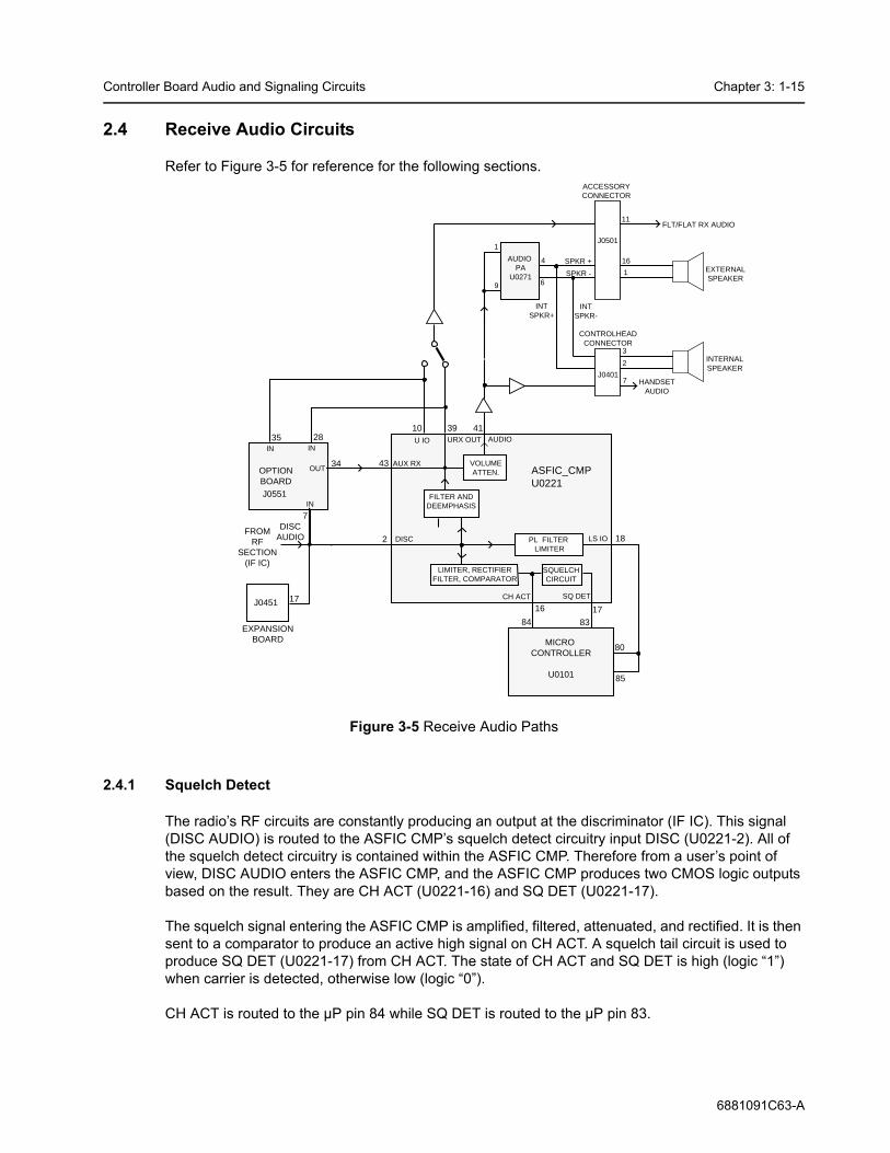
Controller Board Audio and Signaling Circuits Chapter 3: 1-15
2.4 Receive Audio Circuits
Refer to Figure 3-5 for reference for the following sections.
Figure 3-5 Receive Audio Paths
2.4.1 Squelch Detect
The radio’s RF circuits are constantly producing an output at the discriminator (IF IC). This signal (DISC AUDIO) is routed to the ASFIC CMP’s squelch detect circuitry input DISC (U0221-2). All of the squelch detect circuitry is contained within the ASFIC CMP. Therefore from a user’s point of view, DISC AUDIO enters the ASFIC CMP, and the ASFIC CMP produces two CMOS logic outputs based on the result. They are CH ACT (U0221-16) and SQ DET (U0221-17).
The squelch signal entering the ASFIC CMP is amplified, filtered, attenuated, and rectified. It is then sent to a comparator to produce an active high signal on CH ACT. A squelch tail circuit is used to produce SQ DET (U0221-17) from CH ACT. The state of CH ACT and SQ DET is high (logic “1”) when carrier is detected, otherwise low (logic “0”).
CH ACT is routed to the µP pin 84 while SQ DET is routed to the µP pin 83.
FLT/FLAT RX AUDIO
J0501
11
16
1 EXTERNALSPEAKER
INTERNALSPEAKER
ACCESSORYCONNECTOR
CONTROLHEADCONNECTOR
HANDSETAUDIO
7
2
3
J0401
INTSPKR-
SPKR +
SPKR -
1
9
2
J0551
4110
INTSPKR+
4
6
DISC
ASFIC_CMPU0221
AUDIO PA
U0271
IN
OPTIONBOARD
IN
OUTVOLUMEATTEN.
FILTER ANDDEEMPHASIS
17
MICRO CONTROLLER
U0101
80
FROMRF
SECTION(IF IC)
LIMITER, RECTIFIERFILTER, COMPARATOR
SQ DET
SQUELCHCIRCUIT
16
PL FILTER LIMITER
CH ACT
AUX RX43
18LS IO
U IO AUDIO
8384
39URX OUT
17J0451
EXPANSIONBOARD
DISCAUDIO
34
2835
85
IN
7
6881091C63-A
Chapter 3: 1-16 Controller Board Audio and Signaling Circuits
SQ DET is used to determine all audio mute / unmute decisions except for Conventional Scan. In this case CH ACT is a pre-indicator as it occurs slightly faster than SQ DET.
2.4.2 Audio Processing and Digital Volume Control
The receiver audio signal enters the controller section from the IF IC on DISC AUDIO. The signal is DC coupled by R0228 and enters the ASFIC CMP via the DISC pin U0221-2.
Inside the ASFIC CMP, the signal goes through 2 paths in parallel, the audio path and the PL/DPL path.
The audio path has a programmable amplifier, whose setting is based on the channel bandwidth being received, then a LPF filter to remove any frequency components above 3000Hz and then an HPF to strip off any sub-audible data below 300Hz. Next, the recovered audio passes through a de-emphasis filter if it is enabled (to compensate for Pre-emphasis which is used to reduce the effects of FM noise). The IC then passes the audio through the 8-bit programmable attenuator whose level is set depending on the value of the volume control. Finally the filtered audio signal passes through an output buffer within the ASFIC CMP. The audio signal exits the ASFIC CMP at pin AUDIO (U0221-41).
The µP programs the attenuator, using the SPI BUS, based on the volume setting. The minimum / maximum settings of the attenuator are set by codeplug parameters.
Since sub-audible signaling is summed with voice information on transmit, it must be separated from the voice information before processing. Any sub-audible signaling enters the ASFIC CMP from the IF IC at DISC U0221-2. Once inside it goes through the PL/DPL path. The signal first passes through one of 2 low-pass filters, either PL low-pass filter or DPL/LST low-pass filter. Either signal is then filtered and goes through a limiter and exits the ASFIC CMP at LSIO (U0221-18). At this point the signal will appear as a square wave version of the sub-audible signal which the radio received. The µP U0101-80 will decode the signal directly to determine if it is the tone / code which is currently active on that mode.
2.4.3 Audio Amplification Speaker (+) Speaker (–)
The output of the ASFIC CMP’s digital volume pot, U0221-41 is routed through DC blocking capacitor C0265 to a buffer formed by U0211-1. Resistors R0265 and R0268 set the correct input level to the audio PA (U0271). This is necessary because the gain of the audio PA is 46 dB, and the ASFIC CMP output is capable of overdriving the PA unless the maximum volume is limited. Resistor R0267 and capacitor C0267 increase frequency components below 350Hz.
The audio then passes through R0269 and C0272 which provides AC coupling and low frequency roll-off. C0273 provides high frequency roll-off as the audio signal is routed to pins 1 and 9 of the audio power amplifier U0271.
The audio power amplifier has one inverted and one non-inverted output that produces the differential audio output SPK+ / SPK- (U0271-4/6). The inputs for each of these amplifiers are pins 1 and 9 respectively; these inputs are both tied to the received audio. The audio PA’s DC biases are not activated until the audio PA is enabled at pin 8.
The audio PA is enabled via the ASFIC CMP (U0221-38). When the base of Q0271 is low, the transistor is off and U0271-8 is high, using pull up resistor R0273, and the audio PA is ON. The voltage at U0273-8 must be above 8.5VDC to properly enable the device.
6881091C63-A
Controller Board Audio and Signaling Circuits Chapter 3: 1-17
If the voltage is between 3.3 and 6.4V, the device will be active but has its input (U0273-1/9) off. This is a mute condition which is used to prevent an audio pop when the PA is enabled.
The SPK+ and SPK- outputs of the audio PA have a DC bias which varies proportionately with FLT A+ (U0271-7). FLT A+ of 11V yields a DC offset of 5V, and FLT A+ of 17V yields a DC offset of 8.5V. If either of these lines is shorted to ground, it is possible that the audio PA will be damaged. SPK+ and SPK- are routed to the accessory connector (J0501-16 and 1) and to the control head (connector J0401-2 and 3).
2.4.4 Handset Audio
Certain handheld accessories have a speaker within them which require a different voltage level than that provided by U0271. For those devices HANDSET AUDIO is available at control head connector J0401-7.
The received audio from the output of the ASFIC CMP’s digital volume attenuator and buffered by U0211-1 is also routed to U0211-3 pin 9 where it is amplified 20 dB; this is set by the 10k/100k combination of R0261 and R0262. This signal is routed from the output of the op-amp U0211-3 pin 8 to J0401-7. The control head sends this signal directly out to the microphone jack. The maximum value of this output is 6.6Vp-p.
2.4.5 Filtered Audio and Flat Audio
The ASFIC CMP has an audio whose output at U0221-39 has been filtered and de-emphasized, but has not gone through the digital volume attenuator. From ASFIC CMP U0221-39 the signal is routed via R0251 through gate U0251-12 and AC coupled to U0211-2. The gate controlled by ASFIC CMP port GCB3 (U0221-35) selects between the filtered audio signal from the ASFIC CMP pin 39 (URXOUT) or the unfiltered (flat) audio signal from the ASFIC CMP pin 10 (UIO). R0251 and R0253 determine the gain of op-amp U0211-2 for the filtered audio while R0252 and R0253 determine the gain for the flat Audio. The output of U0253-7 is then routed to J0501-11 via DC blocking capacitor C0542 and R0531. Note that any volume adjustment of the signal on this path must be done by the accessory.
2.4.6 RX Secure Audio (Optional)
Discriminator audio, which is now encrypted audio, follows the normal receive audio processing until it emerges from the ASFIC CMP UIO pin (U0221-10), which is fed to the Secure board residing at option connector J0551-35. On the Secure board, the encrypted signal is converted back to normal audio format, and then fed back through (J0551-34) to AUX RX of the ASFIC CMP (U0221-43). From then on it follows a path identical to conventional receive audio, where it is filtered (0.3 - 3kHz) and de-emphasized. The signal URX SND from the ASFIC CMP (U0221-39), also routed to option connector J0551-28, is not used for the Secure board but for other option boards.
2.4.7 Option Board Receive Audio
Unfiltered audio from the ASFIC CMP pin UIO (U0221-10) enters the option board at connector J0551-35. Filtered audio from the ASFIC CMP pin URXOUT (U0221-39) enters the option board at connector J0551-28. On the option board, the signal may be processed, and then fed back through J0551-34 to AUX RX of the ASFIC CMP (U0221-43). From then on it follows a path identical to conventional receive audio, where it may be filtered (0.3 - 3kHz) and de-emphasized.
6881091C63-A

Chapter 3: 1-18 Controller Board Audio and Signaling Circuits
2.5 Receive Signaling Circuits
Refer to Figure 3-6 for reference for the following sections.
Figure 3-6 Receive Signaling Paths
2.5.1 Sub-audible (PL/DPL) and High Speed Data Decoder
The ASFIC CMP (U0221) is used to filter and limit all received data. The data enters the ASFIC CMP at input DISC (U0221-2). Inside U0221 the data is filtered according to data type (HS or LS), then it is limited to a 0-5V digital level. The MDC and trunking high speed data appear at U0221-19, where it connects to the µP U0101-82
The low speed limited data output (PL, DPL, and trunking LS) appears at U0221-18, where it connects to the µP U0101-80.
The low speed data is read by the µP at twice the frequency of the sampling waveform; a latch configuration in the ASFIC CMP stores one bit every clock cycle. The external capacitors C0236, and C0244 set the low frequency pole for a zero crossings detector in the limiters for PL and HS data. The hysteresis of these limiters is programmed based on the type of received data.
2.5.2 Alert Tone Circuits
When the software determines that it needs to give the operator an audible feedback (for a good key press, or for a bad key press), or radio status (trunked system busy, phone call, circuit failures), it sends an alert tone to the speaker. It does so by sending SPI BUS data to U0221 which sets up the audio path to the speaker for alert tones. The alert tone itself can be generated in one of two ways: internally by the ASFIC CMP, or externally using the µP and the ASFIC CMP.
The allowable internal alert tones are 304, 608, 911, and 1823Hz. In this case a code contained within the SPI BUS load to the ASFIC CMP sets up the path and determines the tone frequency, and at what volume level to generate the tone. (It does not have to be related to the voice volume setting.)
For external alert tones, the µP can generate any tone within the 100-3000Hz audio band. This is accomplished by the µP generating a square wave which enters the ASFIC CMP at U0221-19. Inside the ASFIC CMP this signal is routed to the alert tone generator.
DET AUDIODISCRIMINATOR AUDIO
FROM RF SECTION(IF IC)
19
18
25
2
82
80
DISC
PLCAP2
LSIO
HSIODATA FILTERAND DEEMPHASIS LIMITER
FILTER LIMITER
ASFIC_CMPU0221
MICROCONTROLLER
U0101
85
44
8
PLCAP
6881091C63-A

Controller Board Audio and Signaling Circuits Chapter 3: 1-19
The output of the generator is summed into the audio chain just after the RX audio de-emphasis block. Inside U0221 the tone is amplified and filtered, then passed through the 8-bit digital volume attenuator, which is typically loaded with a special value for alert tone audio. The tone exits at U0221-41 and is routed to the audio PA like receive audio
2.6 Voice Storage (Optional)
The Voice Storage (VS) option can be used to store audio signals coming from the receiver or from the microphone. Any stored audio signal can be played back over the radio’s speaker or sent out via the radio’s transmitter.
The Voice Storage option can by placed on the controller section or on an additional board which resides on option board connector J0551. Voice Storage is included on the PassPort board. Voice Storage IC U0301 provides all required functionality and is powered from 3.3 volts regulator U0351 which, is powered from the regulated 5 volts. Dual shottky diode D0301 reduces the supply voltage for U0301 to 3 volts. The µP controls U0301 via SPI bus lines CLK (U0301-8), DATA (U0301-10) and MISO (U0301-11). To transfer data, the µP first selects the U0301 via address decoder U0141, line VS CS and U0301 pin 9. Then the µP sends data through line DATA and receives data through line MISO. Pin 2 (RAC) of U0301 indicates the end of a message row by a low state for 12.5 ms and connects to µP pin 52. A low at pin 5 (INT), which is connected to µP pin 55 indicates that the Voice Storage IC requires service from the µP.
Audio, either from the radio’s receiver or from one of the microphone inputs, emerges the ASFIC CMP (U0221) at pin 39, is buffered by op-amp U0341-1 and enters the Voice Storage IC U0301 at pin 25. During playback, the stored audio emerges U0301 at pin 20. To transmit the audio signal it is fed through resistive divider R0344 / R0345 and line VS MIC to input selector IC U0251. When this path is selected by the µP via ASFIC CMP port GCB 4, the audio signal enters the ASFIC CMP at pin 48 and is processed like normal transmit audio. To play the stored audio over the radio’s speaker, the audio from U0301 pin 20 is buffered by op-amp U0341-2 and fed via switch U0342 and line FLAT RX SND to ASFIC CMP pin 10 (UIO). In this case, this ASFIC CMP pin is programmed as input and feeds the audio signal through the normal receiver audio path to the speaker or handset. Switch U0342 is controlled by the µP via ASFIC CMP port GCB 4 and feeds the stored audio only to the ASFIC CMP port UIO when it is programmed as input.
6881091C63-A
Chapter 3: 1-20 Controller Board Audio and Signaling Circuits
Notes
6881091C63-A

Chapter 3: 2-1
Section 2TROUBLESHOOTING CHARTS
1.0 Troubleshooting Flow Chart for Controller
Power Up Alert Tone
OK?
Speaker & Control
head OK?
U0101EXTAL=
7.3728 MHz/ 14.7456 MHz?
BUS+activity when volume knob
rotated?
MCU is OK
Not able to program
RF Board ICs
Before replacing MCU, check SPI clock, SPI data, and RF IC select
Replace Speaker /
Control Head
U0221 Pin 34 = 16.8 MHz?
Check FGU
Reprogram the correct data. & Check ASFIC
and MCU
Check Control head and MCU (U0101, U0121, U0122, U0111)
Press PTT. No RF Output
Power.
Red LED lights up?
Check Control headCheck
FGU & Transmitter
Audioat Pin 41 U0221?
Enable External PTT with CPS
External PTT enabled with
CPS?
Radio could not PTT
externally
DCat assigned Acc. Con.
Pin DC changes?
Check Components between U0221 and
U0271
Check Connection to µP port
PTT
NO
YES
NO
YESYES
YES
YES
NO
NO
YES
NO
YES
NO
YES
NO
YES
EXTPTT
RXAUDIO
Check Accessories
J0501Audio at Pin
16 & Pin 1
Check Spk. Flex Connection & Control head
Audio at Audio PA
(U0271) input
Check ASFIC U0221
Check Audio PA (U0271)
Check Receiver &
IF IC
Audio at Pin 2
U0221?
NO
NO
NO
YES
YES
NO
YES
NO
Before troubleshooting the controller section according to this chart please check the follow-ing:1. Check tuning and CPS settings2. Check if Alert Tones are enabled3. Check if Control Head is OK4. Check board visually
9.3VDC at Pin 5 of U0641?
YES
NO
5V DC at Pin OUT of
U0651?
YES
NO
Check U0641, Q0641, Q0661, D0660 &
D0661
Check U0651, D0651, D0621
ControllerCheck
6881091C63-A
Chapter 3: 2-2 Troubleshooting Flow Chart for Controller
Notes
6881091C63-A

Chapter 3: 3-1
Section 3CONTROLLER SCHEMATICS AND PARTS LISTS
1.0 Allocation of Schematics and Circuit Boards1.1 Controller Circuits
This chapter shows the schematics and the parts lists for the controller circuits.
1.2 Voice Storage Facility
The Voice Storage facility is an orderable option on all CDM and PRO models except the PassPort model (CDM1550•LS+), on which Voice Storage is a standard feature.
The schematics (including the Voice Storage schematic, where applicable), boards and parts lists for these circuits are shown in this chapter.
Table 3-1 Controller T2 Diagrams and Parts ListsController T2 used on PCB:
8486172B04 VHF, 1-25W
SCHEMATICSController OverallSupply VoltageAudioI/OMicroprocessor
Page:3: 3-33: 3-43: 3-53: 3-63: 3-7
Parts List 3: 3-8
Table 3-2 Controller T5 Diagrams and Parts ListsController T5 used on PCB:
8486172B06 VHF, 1-25W
SCHEMATICSController OverallSupply VoltageAudioI/OMicroprocessorVoice Storage (if fitted)
Page:3: 3-103: 3-113: 3-123: 3-133: 3-143: 3-15
Parts List 3: 3-16
6881091C63-A
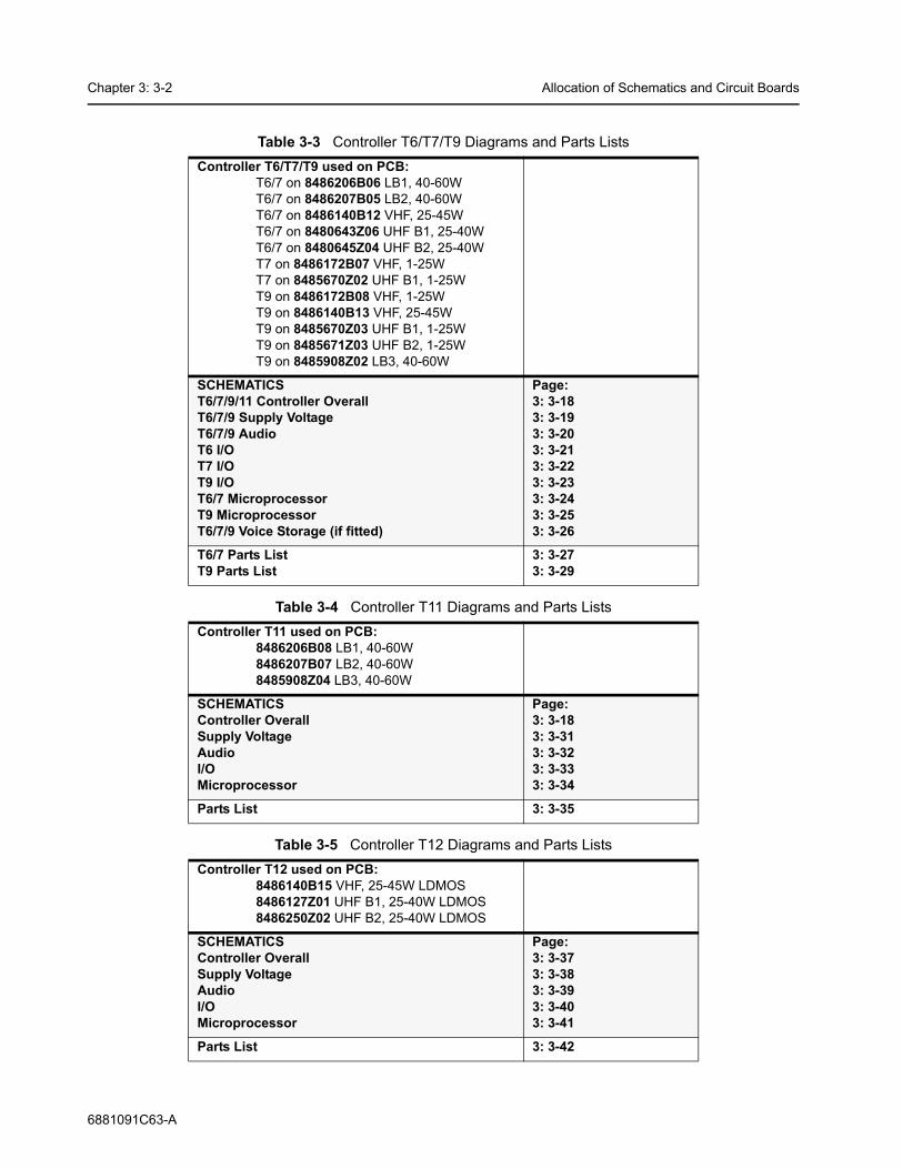
Chapter 3: 3-2 Allocation of Schematics and Circuit Boards
Table 3-3 Controller T6/T7/T9 Diagrams and Parts ListsController T6/T7/T9 used on PCB:
T6/7 on 8486206B06 LB1, 40-60WT6/7 on 8486207B05 LB2, 40-60WT6/7 on 8486140B12 VHF, 25-45WT6/7 on 8480643Z06 UHF B1, 25-40WT6/7 on 8480645Z04 UHF B2, 25-40WT7 on 8486172B07 VHF, 1-25WT7 on 8485670Z02 UHF B1, 1-25WT9 on 8486172B08 VHF, 1-25WT9 on 8486140B13 VHF, 25-45WT9 on 8485670Z03 UHF B1, 1-25WT9 on 8485671Z03 UHF B2, 1-25WT9 on 8485908Z02 LB3, 40-60W
SCHEMATICST6/7/9/11 Controller OverallT6/7/9 Supply VoltageT6/7/9 AudioT6 I/O T7 I/O T9 I/OT6/7 MicroprocessorT9 MicroprocessorT6/7/9 Voice Storage (if fitted)
Page:3: 3-183: 3-193: 3-203: 3-213: 3-223: 3-233: 3-243: 3-253: 3-26
T6/7 Parts ListT9 Parts List
3: 3-273: 3-29
Table 3-4 Controller T11 Diagrams and Parts ListsController T11 used on PCB:
8486206B08 LB1, 40-60W8486207B07 LB2, 40-60W8485908Z04 LB3, 40-60W
SCHEMATICSController OverallSupply VoltageAudioI/OMicroprocessor
Page:3: 3-183: 3-313: 3-323: 3-333: 3-34
Parts List 3: 3-35
Table 3-5 Controller T12 Diagrams and Parts ListsController T12 used on PCB:
8486140B15 VHF, 25-45W LDMOS8486127Z01 UHF B1, 25-40W LDMOS8486250Z02 UHF B2, 25-40W LDMOS
SCHEMATICSController OverallSupply VoltageAudioI/OMicroprocessor
Page:3: 3-373: 3-383: 3-393: 3-403: 3-41
Parts List 3: 3-42
6881091C63-A
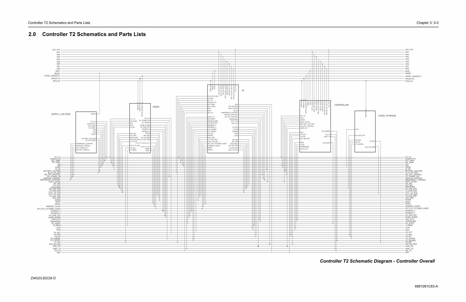
Controller T2 Schematics and Parts Lists Chapter 3: 3-3
6881091C63-A
UART_RX
UART_TX
VSTBY
VS_GAINSEL
VS_INT
VS_RAC
VOICE_STORAGE
5VD
FLAT_RX_SND
RX_AUD_RTN
SP
I(0:1
0)
VS_AUDSEL
VS_INTVS_MIC
VS_RAC
GP
4_IN
_O
UT
_A
CC
8
GP
5_IN
_A
CC
9
GP
6_IN
_A
CC
10
GP
7_IN
_O
UT
_A
CC
12
GP
8_IN
_O
UT
_A
CC
14
GP
IO(0
:13)
LOCK
ON_OFF_CONTROL
OP
T_P
TT
RDY
RE
SE
T
RSSI RX_ADAPT
SCI_TX
SP
I(0:1
0)
TEMPSENSE
CONTROLLER
5VD
BATTERY_VOLTAGE
BOOT_CNTRL
BU
S+
CN
TLR
_A
UD
IO(0
:7)
CNTLVLTG
EXT_BD_REQ
FLT_A+
GP
1_IN
_A
CC
3
GP
2_O
UT
_A
CC
4
GP
3_IN
_A
CC
6
PASUPVLTGFLT_A+
UART_TX
VSTBY
RDY
OPT_PTT
CH_ACT
URX_SND
VS_GAINSEL
MOSBIAS_3
INT_SWB+
EXT_MIC
IN_5V_RF_REG
SCI_TX
VS_MIC
5VD9V3
EXT_SWB+
FLAT_TX_RTN
RX_AUD_RTNDISCAUDIO
INT_MIC
5V_RF
RX_FLAT_FILTERED_AUDIO
HANDSET_AUDIO
SPKR+SPKR-
EMERGENCY_CONTROLIGNITION_CONTROLDC_POWER_ONON_OFF_CONTROL
BATTERY_VOLTAGE
VS_AUDSEL
TEMPSENSE
CNTLVLTG
UART_RX
VS_RACVS_INT
RSSI
LOCK
RX_ADAPT
NOISE_BLNKRPA_PWR_SET
MOSBIAS_2
MODIN
TX_AUD_SNDFLAT_RX_SND
16_8MHZ
TX_AUD_RTN
CNTRL_AUDIO(0:7)
GPIO(0:13)
SPI(0:10)
BUS+
RESET
GP8
GP7
GP6
GP5
GP4
GP3
GP2
GP1
EXP_BD_REQ
BOOT_CNTRL
2
Controller T2 Schematic Diagram - Controller Overall
FLT_A+
IGNITION_CONTROL
INT_SWB+
IN_5V_RF_REG
ON_OFF_CONTROL
PASUPVLTG
RESET
VSTBY
TX_AUD_RTN
TX_AUD_SND
UART_RX
UART_TX
URX_SND
VS_AUDSEL
VS_GAINSEL VS_INT
VS_MIC
VS_RAC
SUPPLY_VOLTAGE
5VD
9V3
BATTERY_VOLTAGE
DC_POWER_ON
EMERGENCY_CONTROL
EXT_SWB+
NOISE_BLNKR
ON_OFF_CONTROL
OP
T_P
TT
PASUPVLTG
PA_PWR_SET
RDY
RE
SE
T
RSSI
RX_ADAPT
RX_AUD_RTN
RX_FLAT_FILTERED_AUDIO
SCI_TX
SP
I(0:1
0)
SPKR+
SPKR-
TEMPSENSE
GP
2_O
UT
_A
CC
4
GP
3_IN
_A
CC
6
GP
4_IN
_O
UT
_A
CC
8
GP
5_IN
_A
CC
9
GP
6_IN
_A
CC
10
GP
7_IN
_O
UT
_A
CC
12
GP
8_IN
_O
UT
_A
CC
14
HANDSET_AUDIO
IGNITION_CONTROL
INT_MIC
INT_SWB+
IN_5V_RF_REG
LOCKMODIN
MOSBIAS_2
MOSBIAS_3
5VD 5V_RF
9V3 BOOT_CNTRL
BU
S+
CH_ACT
CNTLVLTG
DISCAUDIO
EMERGENCY_CONTROL
EXP_BD_REQ
EXT_MIC
EXT_SWB+
FLAT_RX_SND
FLAT_TX_RTN
FLT_A+
GP
1_IN
_A
CC
3
IO
16_8MHZ
TX_AUD_SND
URX_SND
VS_AUDSEL
VS_MIC
FLT_A+
GP
IO(0
:13)
HANDSET_AUDIO
INT_MIC
INT_SWB+
MODIN
MOSBIAS_2
MOSBIAS_3
NOISE_BLNKR
PA_PWR_SET
RX_AUD_RTN
RX_FLAT_FILTERED_AUDIO
SP
I(0:1
0)
SPKR+
SPKR-
TX_AUD_RTN
PASUPVLTGFLT_A+
UART_TX
AUDIO
16_8MHZ
5VD
5V_RF
9V3
CH_ACT
CN
TLR
_A
UD
IO(0
:7)
DC_POWER_ON
DISCAUDIO
EXT_MIC
FLAT_RX_SND
FLAT_TX_RTN
BATTERY_VOLTAGE
VSTBY
RDY
OPT_PTT
CH_ACT
URX_SND
VS_GAINSEL
MOSBIAS_3
INT_SWB+
EXT_MIC
IN_5V_RF_REG
SCI_TX
VS_MIC
5VD9V3
EXT_SWB+
TX_AUD_RTNFLAT_TX_RTN
RX_AUD_RTNDISCAUDIO
INT_MIC
5V_RF
RX_FLAT_FILTERED_AUDIO
HANDSET_AUDIO
SPKR+
SPKR-
EMERGENCY_CONTROLIGNITION_CONTROL
DC_POWER_ONON_OFF_CONTROL
TEMPSENSE
CNTLVLTG
UART_RX
VS_RACVS_INT
RSSI
LOCK
RX_ADAPT
NOISE_BLNKRPA_PWR_SET
MOSBIAS_2
MODIN
TX_AUD_SNDFLAT_RX_SND
16_8MHZ
CNTRL_AUDIO(0:7)
GPIO(0:13)
SPI(0:10)
BUS+
RESET
GP8
GP7
GP6
GP5
GP4
GP3
GP2
GP1
EXP_BD_REQ
BOOT_CNTRL
VS_AUDSEL
.0 Controller T2 Schematics and Parts Lists
ZWG0130228-O
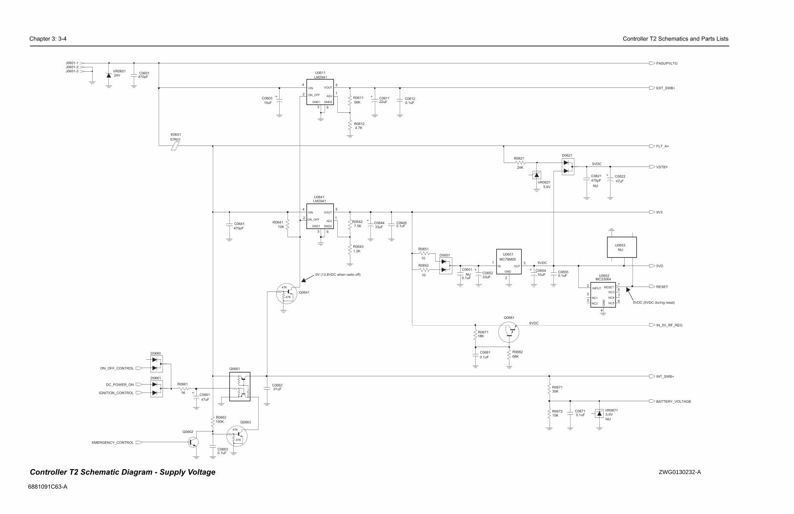
Chapter 3: 3-4 Controller T2 Schematics and Parts Lists
6881091
C0622
47uF
0.1uFC0655
3uF0652
D0621
NU
470pF
C0621
10uFC0654
5.6V
VR0621
MC78M05
2
GND
1IN
3OUT
5.6V
U0651
NU
VR0671
30KR0671
10KR0672 C0671
0.1uF
NU
NC1
3
NC25
NC36
NC47
8NC5
RESET1
U0653
U0652MC33064
GN
D
4
INPUT2
24K
R0621
EXT_SWB+
RESET
9V3
5VD
VSTBY
PASUPVLTG
INT_SWB+
BATTERY_VOLTAGE
FLT_A+
Q0681
IN_5V_RF_REG
68K
R0682
71
uF
681
5VDC
6VDC
5VDC
5VDC (0VDC during reset)
Contr ZWG0130232-A
C63-A
47K
47K
47K
47K
C0663
C0662
0.1uF
.01uF
10
R0652
Q0641
C061122uF
J0601-1
3C
150K
R0662
1.2K
R0643
R0611
56K
0.1uFC0645
33uFC0644R0641C0641
470pF 10K
J0601-2
C06120.1uF
Q0661
U0611
ADJ1
GND1
3
GND2
6
2 ON_OFF
VIN4
VOUT5
LM2941
D0661
1ADJ
GND1
3
GND2
6
ON_OFF2
4VIN
5VOUT
LM2941U0641
Q0662
R0651
57R01
10
R0642
E0631
J0601-3
7.5K
C0601
C0603
470pF
10uF
R0661
1KC0661
47uF
D0651
0.1uFNU
C0651
Q0663
D0660
4.7K
24V
R0612
VR0601
DC_POWER_ON
IGNITION_CONTROL
EMERGENCY_CONTROL
ON_OFF_CONTROL
R0618K
0.1
C0
0V (13,8VDC when radio off)
oller T2 Schematic Diagram - Supply Voltage

Controller T2 Schematics and Parts Lists Chapter 3: 3-5
6881091C63-A
0.1uF
C0262
C0261
82pF
NU
C0251
0.1uF
NU
R0275
1000pF
C0276
10K
24K
R0273
R0262
100K
74
11
MC3403
U0211-2
6
5
R0276
15K
40311-1
R0269470
Q0271
INV9
M_SS8
NINV1
4OUT1
OUT26
3RR
VC
C
7
U0271
GN
D1
2 5
GN
D2
C0273
3300pF
47uF
C0275
C0252
1uF
0.1uFC0272
10K
R0261
C0271.01uF
E0271
57R01
57R011000pF
E0272C0277
4Z
ND
VC
C
7
VEE
14X
15Y
B
A11
10B
9C
6EN
51
100K
R0253
MC3403
U0211-413
1214
4
11
MC3403
9
10
8
4
11
MC3403
U0211-3
C0253
100pF
NU
NU
10K
R0274
NU0.1uF
C0274
9V3
9V3
MODIN
V3
16_8MHZ
SPKR-
FLT_A+
SPKR+
9V3
VS_AUDSEL
SPI(0:10)
GPIO(0:13)
CNTLR_AUDIO(0:7)
VAG
VAG
HANDSET_AUDIO
RX_FLAT_FILTERED_AUDIO
PA
13VDC unmuted5VDC muted
5VDC RX FilteredAudio (0V DC Flat)
630mV RX Filtered330mV Flat
0 VDC
Controller T2 Schematic Diagram - Audio
SY
N
F1200
CLK
GP
2_O
UT
CS
X
DA
TA
LS
IO
VO
X
SQ
_D
ET
HS
IO
CH
_A
CT
R025147K
C0204
0.1uF
C0235
C0231
.022uF
4.7uF
5
10uF
C0212
R0206
10K
2
NU
0.22uF
C0224
100pF
C0233
R0208
0.1uF
2.2K
C0222
100pFC0243
2200pF
C0203
NU
0.1uF
C0227
6
MC3
2
31
4
11 U02
24K
R0221
NU0.1uF
C02650.1uF
C0266
4
.033uF
C0236
0.1uFC0245
C0232
9
0.1uF
0
NU
R0242
C0242
0.1uF
0.1uFC0241
C0267
.01uF 47K
10K
R0267
R0268
R0265
24K
10uF
C0201
NU
2200pF
D0201
NU
C0205
10K
R0205
R0252
56K
7
560
R0202
TP0221
1
1
7
0.1uF
R0223
C0226
30K
0.1uF
C0221
.01uF
C0246
3
R02072.2K
R022224K
0.1uFC0244
C0254
0.1uF
C02550.1uF
7.5K
R0212
R0211
Y15
Z0
Z13
7.5K
G
12X0
13X1
2Y0
1
MC14053
8
45
VD
DR
C
27VDDSYN
7VOX
U02
36TXRTN
44
TX
SN
D
10UIO
39
UR
XO
UT
1VDDA
32VDDCP
33VDDD
11VDDDAC
46
MIC
INT
40
MO
D
26NC
8PLCAP
25PLCAP2
17
SQ
DE
T
9SQIN
28SYN
31GNDD
30GNDD0
47
GN
DR
C
23
GN
DS
YN
19
HS
IO
LC
AP
24
18
LS
IO
48
MIC
EX
T
29F1200
15
GC
B0
14
GC
B1
13
GC
B2
35GCB3
GC
B4
37
38
GC
B5
3GNDA
21
CLK
34CLK168
20
CS
X
6DACG
5DACR
DACU4
22
DA
TA
2DISC
12AGCCAP
41
AU
DIO
AU
XR
X4
3
42
AU
XT
X
16
CH
AC
T
63A53
U0221
1
TP0222
R0266
24K
NU
NU
0.1uF
560
8
C0211
R0204
100
R0201
R0224
11
8.2K
47K
R0241
C0223
0.1uF
0.1uF
C0234
0.1uF
C0225
INT_SWB+
CH_ACT
VAG
9V3 9V3
9
VS_MIC
MOSBIAS_3
VAG
EXT_MIC
TX_AUD_SND
5V_RF
5V_RF
5VD5VD
5V_RF
5V_RF5V_RF
5V_RF
5V_RF
TX_AUD_RTN
RX_AUD_RTN
INT_MIC
URX_SND
FLAT_RX_SND
DC_POWER_ON
ASFIC CMP
5VD
5VD
DISCAUDIO
PA_PWR_SET
MOSBIAS_2
FLAT_TX_RTN
NOISE_BLNKR
2.2uFNU
C0237
R0224
8.2K
NU
R0226
1M
R0227
1M
4.6VDC
80mV RMS
80mV RMS
5VDC (0VDC during radio off)
300mV RMS
200mV RMS
145mV RMS @25kHz72mV RMS @12.5kHz
ZWG0130231-A
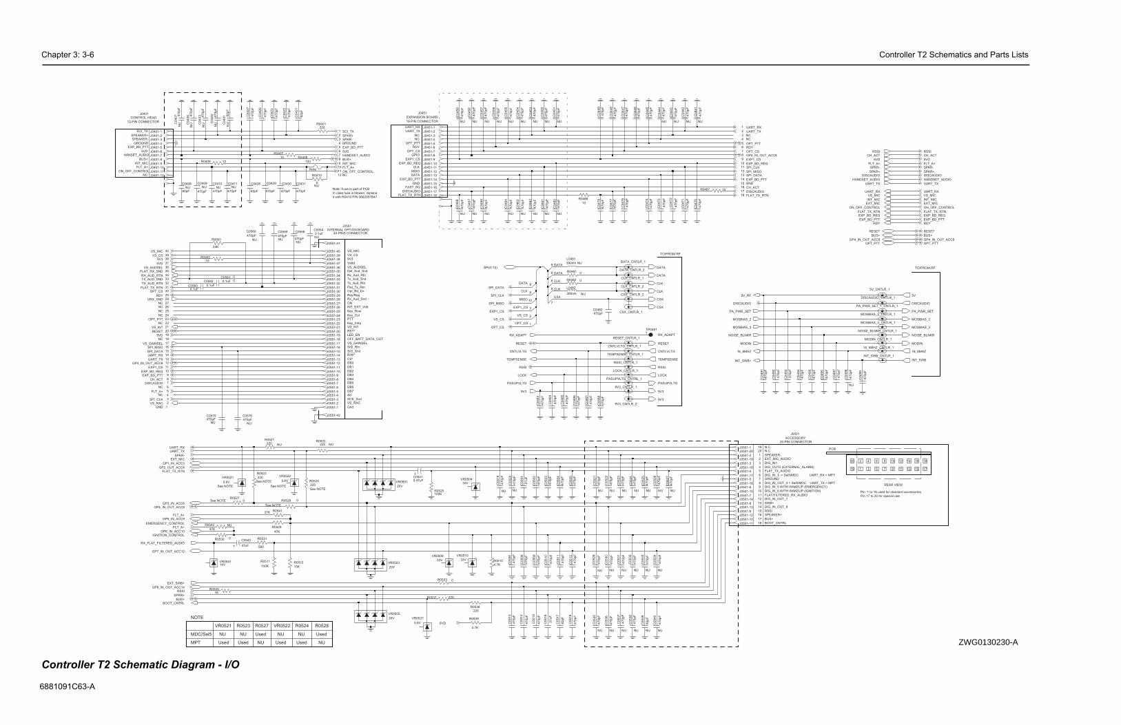
Chapter 3: 3-6 Controller T2 Schematics and Parts Lists
6881091
SPEAKER+
BUS+
1
DIG_IN_OUT_8
RSSI
7
4
18
17
13 15 17
64
DIG_IN_5 WITH WAKEUP (EMERGENCY)
13
9 11
DIG_IN_OUT_4 = Sel5/MDC UART_TX = MPT
9
DIG_IN_3 = Sel5/MDC UART_RX = MPT
20
1 3
15
REAR VIEW
PCB
2
5
14
NC
16
FLAT_TX_AUDIO
19
20
ACCESSORY
9
10 DIG_IN_6 WITH WAKEUP (IGNITION)
FLAT/FILTERED_RX_AUDIO
DIG_IN_OUT_7
DIG_OUT2 (EXTERNAL_ALARM)
SPEAKER-
11
3
4
5
8
SWB+
16 18
6
16
6
GROUND
5
3
TO/FROM RF
7
NC
N.C.
2
1
GND
18
DIG_IN1
20-PIN CONNECTOR
J0501
2
15
14
13
10
8
719
17
BOOT_CNTRL
EXT_MIC_AUDIO
12
N.C.
1412108
11
12
10R0467
PA_PWR_SET
J0501-17
J0501-5
NOISE_BLNKR_CNTLR_1
C0
49
6
47
0p
F
16_8MHZ_CNTLR_1
47
0p
F
C0
49
7
MODIN
47
0p
F
C0
49
2
47
0p
F
C0
49
5
C0
47
1
47
0p
F
C0
47
0
47
0p
F
J0501-20
MOSBIAS_2_CNTLR_1
C0
44
1
47
0p
F
NU
J0501-1
J0501-15
NOISE_BLNKR
J0501-10
J0501-11
C0
49
3
J0501-12
47
0p
F
DISCAUDIO_CNTLR_1
J0501-16
MOSBIAS_3_CNTLR_1
J0501-8
C0
44
2
J0501-2
47
0p
F
NU
J0501-19
47
0p
F
C0
49
4
MODIN_CNTLR_1
J0501-13
J0501-3
C0
49
8
NU
47
0p
F
16_8MHZ
J0501-7
J0501-6
J0501-4
J0501-18
DISCAUDIO
MOSBIAS_2
MOSBIAS_3
PA_PWR_SET_1_CNTLR_1
5V
C0
49
1
47
0p
F
J0501-14
5V_CNTLR_1
J0501-9
DISCAUDIO
HANDSET_AUDIOHANDSET_AUDIO
UART_TX
UART_RX
RSSI RSSI
UART_TX UART_TX
UART_RXUART_RX
RDYRDY
OPT_PTT
OPT_PTTOPT_PTT
INT_MIC INT_MIC
SPKR+SPKR+
DISCAUDIO
EXP_BD_REQEXP_BD_REQ
EXP_BD_PTT EXP_BD_PTT
CH_ACT CH_ACT
OPT_CS
RDY
GP4_IN_OUT_ACC8
SPI_CLK
EXP_BD_PTT
DISCAUDIO
MOSBIAS_3
VS_MIC VS_MICFLAT_TX_RTN
DISCAUDIO
16_8MHZ
5V_RF
MODIN
NOISE_BLNKR
MOSBIAS_2
PA_PWR_SET
FLAT_TX_RTN FLAT_TX_RTN
GP4_IN_OUT_ACC8 GP4_IN_OUT_ACC8
CH_ACT
SPI_DATA
SPI_MISO
EXP_BD_REQ
EXP1_CS
BUS+ BUS+
RESETRESET
ON_OFF_CONTROL ON_OFF_CONTROL
EXT_MICEXT_MIC
SPKR-SPKR-
5VD5VD
FLT_A+FLT_A+
INT_SWB_CNTLR_1
INT_SWBINT_SWB+
C0
49
9
47
0p
F
Pin 1 to 16 used for standard accessories
Pin 17 to 20 for special use
ZWG0130230-A
Contr
C63-A
32
31
11
7
17
12
10
VS_CS
INT_MIC
26
Gnd
RST*
VS_MIC
DB1
36
39
38
30
33
37
DB2
Key_Intrp
9V3
LED_EN
DB0
DATA
Tx_Aud_Snd
Tx_Aud_Rtn
PTT
Vddd
25
6
J0551
9
3
2
1
NC
9
7
8
NC
NC
10
11
12
4
DATA
CLK
8
NC
GROUND
Rx_Aud_Rtn
Rdy/Req
EXPANSION BOARD
18-PIN CONNECTOR
DATA
SCI_TX
EXP_BD_PTT
GND
FAST_SQ
DISCAUDIO
INTERNAL OPTION BOARD
23
21
19
20
16
15
14
13
5
28
29
12-PIN CONNECTOR
DB7
NC
24NC
NC
DB6
5VD
HANSET_AUDIO
CONTROL HEAD
BUS+
VS_GAINSEL
OFF_BATT_DATA_OUT
FLT_A+
Key_Col
TO/FROM RF
VS_RAC
NC
NC
NC
GND
CSX
RX_ADAPT
CLK
MISO
4
VS_CS
Flat_Tx_RtnCLK
SrD_Rtn
EXP1_CS
CLK
MISO
EXP_BD_PTT
DB3
J0401
SrD_Snd
Rx_Aud_Snd
ON
VS_INT
1
2
3
5
6 OPT_CS
RDY
OPT_PTT
NC
NC
FLAT_TX_RTN
ON_OFF_CONTROL
J0451
A0
Key_Row
VS_AUDSEL
GPIO
EXP1_CS
EXP_BD_REQ
INT_EXT_Vdd
R/W*
Opt_Bd_En
CS*
27
22
18
40-PINS CONNECTOR
SPEAKER-
SPEAKER+
GROUND
UART_TX
UART_RX
Det_Aud_Snd
40
OPT_CS
DB4
DB5
SCK_Snd
35
34
DATA
47
0p
F
C0
51
0
J0451-2
J0401-10
J0401-7
47
0p
F
J0551-19
C0
50
1
C0
42
6
.01
uF
J0401-2
J0401-1
47
0p
FN
UC0
40
3
C0
40
2N
U
C0
45
7
NU
47
0p
F
NU
47
0p
F
47
0p
F
C0
45
8
C0
45
9
NU
47
0p
F
J0551-42
J0551-41
J0551-1
VR0509
33V
C0
52
4
47
0p
F
NU
47
0p
F
NU
C0
45
4
C0
52
8
47
0p
F
NU
C0428
9V3
R0410
82pF
0NU
VR0537
5.6V
C0
47
3
47
0p
F
47
0p
F
C0
47
4
C0
47
6
47
0p
F
8
NU470pF
C0558
470pF
CSX_CNTLR_2
CSXC0482
C0410NU
470pF
J0551-5
47
0p
F
NU
47
0p
F
NU
C0
52
3
47
0p
F
NU
C0
53
1
C0
53
0
VR0505
20V
C0
48
7
47
0p
F
33V
VR0510
C0
44
9
47
0p
F
J0401-3
PASUPVLTG
LOCK
J0551-37
82
pF
NU
DATA
C0
53
9
J0551-32
J0551-33
J0551-28
J0451-16
9
RSSI_CNTLR_1
NUC0411
470pF
9V3
J0551-27
VR0521 VR0522
5.6V 5.6V
NU220R0522
NU220R0521
RSSI
NU390nH
L0481
10
DATA
R0407
C0
52
7
47
0p
F
NU
C0
52
6
47
0p
F
NU
47
0p
F
NU
47
0p
F
C0
54
0
C0
42
3
470pF
C0431
47
0p
F
C0
42
2
47
0p
F
NU
C05410.47uF
C0
52
5
J0551-24
R0525100K
9V3_CNTLR_1
NU
9
C0
53
5
47
0p
F
VR0501
20V
C0
47
2
47
0p
FR0468
10
J0551-6
J0551-7
220
R0524220
R0523
14VVR0541
CNTLVLTG_CNTLR_1
NU
47K
R0542
C0
46
7
NU
47
0p
F
J0401-12
J0451-10
C0
50
9
47
0p
F
J0451-17
J0551-34
R0409 10
J0551-8
J0551-9
C0
51
5
J0551-10
47
0p
F
R0535
J0451-14
1K
C0
45
6
C0
52
0
CLK
NU
47
0p
F
C0
40
7
NU
47
0p
F
47
0p
FN
U
C0
44
8
47
0p
F
C0
44
7
47
0p
F
J0451-18
9
8
C0
48
6
47
0p
F
C0429
470pF
C0
45
3
NU
47
0p
F
NU
47
0p
F
C0
45
5
47
0p
F
NU
C0
46
8
J0451-9
C0
48
5
47
0p
F
NU
C0
46
2
47
0p
F
LOCK_CNTLR_1
J0551-30
J0551-35
C0
50
5
47
0p
F
J0551-38
C0
53
8
47
0p
FNU
C0408NU
82pF
47
0p
F
NU
C0
53
4
C0
53
3
47
0p
F
NU
C0
53
2
47
0p
F
NU
C0
46
4
47
0p
F
NU
J0551-11
J0551-2
J0551-16
0.1uFC0593
NU0.1uF
C0554
0R0533
47
0p
F
NU
C0
52
1
C0
48
8
47
0p
F
C0
50
8
47
0p
F
C0
51
1
C0
51
2
47
0p
F
CLK
47
0p
F
2
47
0p
F
C0
47
7
NU
470pF
47K
CSX
C0560
R0529
J0551-21
J0401-11
J0451-5
J0551-3
C0576
NU
470pF
PASUPVLTG_CNTRL_1
VR0503
20V
J0401-4
R059210
C0591
0.1uF
9V3_CNTLR_2
J0451-6
TEMPSENSE_CNTLR_1
47
0p
F
NU
C0
44
3
C0
46
3
NU
47
0p
F
J0551-14
J0551-4
VR0504
47
0p
F
C0
50
4
33V
NU
47
0p
F
C0
51
9
C0
42
7
47
0p
F
J0451-3
C0
51
6
.01
uF
J0451-12
C0
52
2
47
0p
F
NU
NU470pF
C0575
C0559
RESET
TEMPSENSE
NU470pF
C0
53
7
47
0p
F
NU
47
0p
F
C0
51
3
47
0p
F
C0
47
8
0R0482
R0481 0
8CLK_CNTLR_2
C0
44
5
47
0p
F
C0
44
6
47
0p
F
J0451-13
J0551-26
220R0537
47
0p
F
C0
51
4
J0551-36
NU
47
0p
F
NU
47
0p
F
C0
44
4
C0
46
1
0R0527
0R0528
J0551-15
82
pF
C0
51
7
J0551-25
J0401-8
J0401-5
J0551-31
47
0p
F
NU
C0
53
6
47
0p
F
C0
48
4
47
0p
F
NU
C0
46
6
J0551-18
J0551-23
J0551-17
47
0p
F
NU
C0
46
0
27K R0541
C0430
470pF
82
pF
J0401-6
C0
42
1
J0451-1
0.1uF
C0592
C0
40
6N
U4
70
pF
1
10
J0551-22
RESET_CNTLR_1
0R0530
R0401220
CLK_CNTLR_1
C0
51
8
47
0p
F
NUC
04
01 8
2p
F
47
0p
F
C0
50
2
J0551-13
J0451-7
R0591
J0451-8
100K
24K
R0511
CSX_CNTLR_13
C0
48
3
47
0p
F
J0551-40
DATA_CNTLR_2
J0551-20
C0409
470pF
J0451-11
NU
4.7K
4.7K
R0539
R0510
DATA_CNTLR_1
J0451-4
J0451-15
47
0p
F
C0
50
6
R0538
220
J0551-39
J0551-12
CNTLVLTG
C0542
TP04811
47uF
J0551-29
15K
R0512
C0
50
3
390nH NU
47
0p
F
J0401-9
7
L0482
560
R0531
C0
45
1
NUNU
47
0p
F
47
0p
F
HANDSET_AUDIO
UART_RX
UART_TX
GP6_IN_ACC10
BOOT_CNTRL
5VD
C0
45
2
FLT_A+
BUS+
5VD
RSSI
EXT_SWB+
UART_TX
UART_RX
GP4_IN_OUT_ACC8
GP3_IN_ACC6
RDY
OPT_PTT
INT_MIC
GP7_IN_OUT_ACC12
5VD
GP4_IN_OUT_ACC8
EXP1_CS
EXP_BD_REQ
EXP_BD_PTT
CH_ACT
DISCAUDIO
FLT_A+
SCI_TX
SPKR+
GP1_IN_ACC3
RX_FLAT_FILTERED_AUDIO
EMERGENCY_CONTROL
GP5_IN_ACC9
SPKR+
SPKR-
ON_OFF_CONTROL
EXP_BD_PTT
SPI(0:10)
RX_ADAPT
EXT_MIC
SPKR-
FLAT_TX_RTN
EXP1_CS
9V3
GP8_IN_OUT_ACC14
FLT_A+
FLAT_TX_RTN
RESET
RESET
PASUPVLTG
BUS+
GP2_OUT_ACC4
9V3
TEMPSENSE
CNTLVLTG
RSSI
LOCK
SPI_DATA
SPI_CLK
SPI_MISO
VS_CS
OPT_CS
OPT_CS
SPI_DATA
TX_AUD_RTN
VS_CS
VS_MIC
SPI_CLK
FLAT_RX_SND
RX_AUD_RTN
URX_SND
TX_AUD_SND
VS_INT
5VD
VS_AUDSEL
VS_GAINSEL
SPI_MISO
VS_RAC
IGNITION_CONTROL
FLT_A+
See NOTE
See NOTE
See NOTE
See NOTE
See NOTESee NOTE
100
R0408
NOTE
VR0521 R0523 R0527 VR0522 R0524 R0528
MDC/Sel5 NU NU Used NU NU Used
MPT Used Used NU Used Used NU
Note
Note: Fuse is part of PCB
In case fuse is blowen, replace
it with R0410 P/N 0662057B47
oller T2 Schematic Diagram - I/O

Controller T2 Schematics and Parts Lists Chapter 3: 3-7
6881091C63-A
47K
47K
47K
47K
47K
47K
47K
47K
47K
47K
GP6_IN
GP4_IN
GP3_IN
GP4_IN
VS_CS
EXP1_CS
GP1_IN
GP7_IN
HC138_A0
OPT_CS
HC138_A1
HC138_A2
GP5_IN
GP6_IN
GP8_OUT
HC138_A1
H/W-Version &
Memory size
GP4_OUT
GP7_OUT
BD_PTT & DATA_PTT)
EE_CS
GP2_OUT
GP8_OUT
LVZIF_CS
REF_CS
HC138_A2
EXP2_CS
GP7_IN
GP8_IN
GP8_IN
GP3_IN
PE6
HC138_A0
GP5_IN
1
0
GP4_OUT
GP7_OUT
Q0177
7
47KR0186
1000pFC0107
Q0181
C0106100pFNU
10
0.1uF
Y510
Y69
Y77
C0141
EN_CS35
GN
D
8
VC
C
16
Y015
Y114
Y213
Y312
Y411
A01
A12
A23
EN_CS16
EN_CS24
U0141
MC74HC138A
5
6
9
47KR0178
103
8
11
1
2
3
4.7K
R0183
3
12
24KR0152
24K
13
0
R0151
47K
R0182
R0176
5
30K
12
R0175
10K
13
10
1
3
R010410K
7
R0114
10K10KR0113
R01814.7K
4.7K
R0185
5
9
2
4.7K
R0177
Q0183
4
R0179
47K
D0179
4
10K
47KR0184
R0174
R0108
2.2K
See
NOTE
100KR0105
4
2
0
6
Q0173
0
See
NOTE
R0106
8
10K
R0170
Q0185
GP3_IN_ACC6
GPIO(0:13)
GPIO(0:13)
FROM_U0101_46
FROM_U0101_47
VS_RAC
5VD
VS_INT
GP4_IN_OUT_ACC8IRQ
5VD
5VD
RESET
RESET
5VD
5VD
GP5_IN_ACC9
BATTERY_VOLTAGE
5VD
FLT_A+ GP2_OUT_ACC4
TEMPSENSE
VS_GAINSEL
EXT_BD_REQ
RSSI
5VD
5VD
ECLK
LOCK
GP7_IN_OUT_ACC12
GP8_IN_OUT_ACC14
5VD
5VD
5VD
GP6_IN_ACC10
5VD
R_W
VSTBY
CNTLVLTG
3.9K
R0117
Q0171
4.7K
R01715VD10K
R0172
GP1_IN6
5VD
GP1_IN_ACC3
R01734.7K
NOTE
R0105 R0106 R0128 R0109 U0125
MDC/Sel5 Used NU NU Used NU
MPT NU Used Used NU Used
Controller T2 Schematic Diagram - Microprocessor
ZWG0130229-A
47K
47K
47K
47K
16Kx8bit
HS
IO
CL
K
VO
X
LS
IO
ON_OFF_SENSE
EEPROM
MIS
O
CL
K
F1
20
0
CH
AC
T
SQ
_D
ET
512kx8bit
(EXT_
RAM
FL
AS
H R
OM
GP4_OUT
GP7_OUT
MIS
O
SY
N
LS
IO
32kx8bit
EE
_C
S
DA
TA
CS
X
HS
IO
MICROPROCESSOR
DA
TA
R0121
100K
0NU
3
5
R0116
8
4
3
C0123100pF
NU
15IO4
16IO5
17IO6
18IO7
19IO8
28
VC
C
24A9
20EN_CS
22EN_OE
27EN_WE
GN
D
14
11IO1
12IO2
13IO3
1A14
8A2
7A3
6A4
A55
4A6
3A7
25A8
U0122
10A0
9A1
A1021
23A11
2A12
26A13
3
2
5
Q0110
27K
NU
0
2
R0125
100pFNU
C0104
10MEG
9
R0131
7
C0111
100pFNU
XTL0 7
XTL112
0
RS013
RS114
RTS
R_W*28
10TD
VS
SV
DD
15
D119
D018
DCD16
DSR17
DTR 11
RC5
RD12
CS13
CTS9
D7 25
D6 24
D5 23
D422
D321
D220
U0125
CLK
CS02
6
3
R0101
10K
5
8
R010747KNU
1
6
18
TP0102
0.1uFC0121
0.1uF
TP01
C0122
27KNU
98
R0126
6
6
0
1
22pF
4
C0131
D0101
5.6V
VR0151
75
D0151
.01uF
6
11
12
C0151
4
0
6
R0128See NOTE
R0132
330K
7
SI 5
SO2
VC
C
8
VS
S
4
WP 3
2
X25128_2.7V
CLK6
CS 1
HOLD
013
U0111
12
11
10
100pF
0
C0101
1
10
1
7
7
TP0151
10K
R0115
0R0111
R011010KNU
C0112
0.1uF
22pF
2
C0132
0
1
7
TP0101
4
11
5
14
9
4
1
10
810
16
NCNC1
OUT IN
R0109
Y0131
38.40KHz
XTAL
R0112
0NU
18
4.7KR0102
14
C0103100pFNU
6
7
6
5
8
15
15
9
4
13
12
14
13
17
40
VS
SL
87
VS
SR
XF
C9
3
48XIRQ
91
XT
AL
94RESET
12
VD
D
39
VD
DL
88
VD
DR
92
VD
DS
YN
69
VR
H
68
VR
L
13
VS
S
71PJ0_CSGP3
72PJ1_CSGP4
73PJ2
74PJ3
75PJ4
76PJ5
77PJ6
78PJ7
56
PI0
55
PI1
54
PI2
53
PI3
52
PI4
51
PI5
50
PI6
49
PI7
47PH0_PW1
46PH1_PW2
45PH2_PW3
44PH3_PW4
43PH4_CSIO
42PH5_CSGP1
41PH6_CSGP2
38PH7_CSPROG
6PG0_XA13
16PG1_XA14
20PG2_XA15
19PG3_XA16
17PG4_XA17
18PG5_XA18
5PG6_AS
4PG7_R_W
28
PF
1_
AD
DR
1
27
PF
2_
AD
DR
2
26
PF
3_
AD
DR
3
25
PF
4_
AD
DR
4
24
PF
5_
AD
DR
5
23
PF
6_
AD
DR
6
22
PF
7_
AD
DR
7
29
PF
O_
AD
DR
0
PE0_AN067
PE1_AN166
PE2_AN265
PE3_AN364
PE4_AN463
PE5_AN562
PE6_AN661
PE7_AN760
37PC7_DATA7
97
PD
0_
RX
D
98
PD
1_
TX
D
99
PD
2_
MIS
O
10
0P
D3
_M
OS
I
1P
D4
_S
CK
2P
D5
_S
S
PD
6_
LV
IN3
14
PB
O_
AD
DR
8
30PC0_DATA0
31PC1_DATA1
32PC2_DATA2
33PC3_DATA3
34PC4_DATA4
35PC5_DATA5
36PC6_DATA6
86
PA
7_
PA
1_
OC
1
10
PB
1_
AD
DR
9
11
PB
2_
AD
DR
10
9P
B3
_A
DD
R1
1
21
PB
4_
AD
DR
12
15
PB
5_
AD
DR
13
8P
B6
_A
DD
R1
4
7P
B7
_A
DD
R1
5
57MODB_VSTBY
79
PA
0_
IC3
80
PA
1_
IC2
81
PA
2_
IC1
82
PA
3_
IC4
_O
C5
_O
C1
83
PA
4_
OC
4_
OC
1
84
PA
5_
OC
3_
OC
1
85
PA
6_
OC
2_
OC
1
59
AV
DD
70
AV
SS
89ECLK
90
EX
TA
L
96IRQ
LV
OU
T9
5
58MODA_LIR
U0101
MC68HC11FL0
Q0151
7
3
2
1
0
C0105
NU100pF
3
2
1
26
IO527
IO628
IO729
8
VC
C
10
9
1
30
EN_OE32
EN_WE7
24
GN
D
21IO0
IO122
IO223
IO325
IO4
18
A317
A416
15A5
14A6
A713
A83
A92
EN_CE
1
A1212
4A13
A145
11A15
A1610
A176
A189
A2
A020
A119
A1031
A11
16
3
U0121
1
1
100pFNU
C0102
7
4
2
17
5VD
ON_OFF_CONTROL
R_
WR
AM
_C
S
SCI_TX
BUS+
5
3
5VD
SPI(0:10)SPI(0:10) SPI(0:10) SPI(0:10) SPI(0:10)
CNTLR_AUDIO(0:7) CNTLR_AUDIO(0:7)CNTLR_AUDIO(0:7)CNTLR_AUDIO(0:7)
FROM_U0101_47
FROM_U0101_46
UART_CS
IRQ
BOOT_CNTRL
FLASH_CE
FLASH_OE
R_W
5VD
5VD
ECLK
R_W
5VD
ADDR_BUS(0:18)
UART_RXUART_TX
5VD
5VD
OPT_PTT
RAM_CS
5VD
RX_ADAPT
5VD5VD
FLT_A+ FLT_A+
FLASH_OE
UART_CS
DATA_BUS(0:7)
NC
_X
TA
L
NC
_P
B6
_A
DD
R1
4
NC
_P
B7
_A
DD
R1
5
RDY
ON_OFF_CONTROL
NC_PH5_CSGP1
FLASH_CE
5VD
See NOTE
8
26
5VD
0
NU
R0124
0
NU
R0127
0.1uF
NU
C0125
5VD
1
27
UART
1
23
4
5VDC (0VDC during On/Off pressed
and during head request)
5VDC (0VDC during boot mode)
0 0

Chapter 3: 3-8 Controller T2 Schematics and Parts Lists
688109
Contr
CirR
C010C010C011C012C012C012C013C013C014C015C020C020C021C022C022C022C022C022C022C022C023C023C023C023C023C024C024C024C024C024C025C025C025C026C026C026C026
pFpFpFpFpFpFpFpFFpFpFpFpFpFpFpFpFpFpFpFpFpFFFpFuF
F FFF
pFFFF
FpFFF
Description
C0652 2311049A97 33uFC0654 2311049A57 10uFC0655 2113743E20 0.1uFC0661 2311049C05 47uFC0662 2113741F49 .01uFC0663 2113743E20 0.1uFC0671 2113743E20 0.1uFC0681 2113743E20 0.1uFD0101 4880236E05 Chip SchottkyD0151 4813833C02 DUAL SOT MMBD6100D0179 4813833C02 DUAL SOT MMBD6100D0621 4813833C02 DUAL SOT MMBD6100D0651 4813833C02 DUAL SOT MMBD6100D0660 4813833C02 DUAL SOT MMBD6100D0661 4813833C02 DUAL SOT MMBD6100E0271 2484657R01 Ferrite BeadE0272 2484657R01 Ferrite BeadE0631 2484657R01 Ferrite BeadJ0401 0902636Y02 CONN FLEX 12 PINJ0451 0902636Y01 CONN FLEX SIDE ENTRYJ0501 0986105B01 CONN SMD 20 PINJ0551 0905505Y04 CONN ZIF HORIZONTALJ0601 0986165B01 DC PWR CONNQ0110 4880048M01 NPN DIG 47k/47kQ0151 4880048M01 NPN DIG 47k/47kQ0171 4880048M01 NPN DIG 47k/47kQ0173 4880052M01 NPN DRLNGTN MXTAQ0177 4880048M01 NPN DIG 47k/47kQ0181 4880048M01 NPN DIG 47k/47kQ0183 4880048M01 NPN DIG 47k/47kQ0185 4880048M01 NPN DIG 47k/47kQ0271 4813824A10 NPN 40V .2AQ0641 4880048M01 NPN DIG 47k/47kQ0661 4805921T02 DUAL ROHM FMC2 RHQ0662 4813824A10 NPN 40V .2A B=50-150Q0663 4880048M01 NPN DIG 47k/47kQ0681 4880052M01 NPN DRLNGTN MXTAR0101 0662057A73 10K 1/16W 5%
Circuit Ref
Motorola Part No. Description
1C63-A
oller T2 Parts List
cuit ef
Motorola Part No. Description
1 2113740F51 100pF7 2113741F25 1000pF2 2113743E20 0.1uF1 2113743E20 0.1uF2 2113743E20 0.1uF5 2113743E20 0.1uF1 2113740F35 22pF2 2113740F35 22pF1 2113743E20 0.1uF1 2113741F49 .01uF1 2311049A57 10uF4 2113743E20 0.1uF2 2311049A57 10uF1 2113743E20 0.1uF2 2113743E20 0.1uF3 2113743E20 0.1uF4 2113740F51 100pF5 2113743E20 0.1uF6 2113743E20 0.1uF7 2113743E20 0.1uF1 2113743G24 2.2uF2 2113743E20 0.1uF4 2113743E20 0.1uF5 2113743E07 .022uF6 2113743E10 .033uF1 2113743E20 0.1uF3 2113740F51 100pF4 2113743E20 0.1uF5 2113743E20 0.1uF6 2113741F49 .01uF2 2311049A07 1uF 4 2113743E20 0.1uF5 2113743E20 0.1uF1 2113743E20 0.1uF2 2113740F49 82pF 5 2113743E20 0.1uF7 2113741F49 .01uF
C0271 2113741F49 .01uFC0272 2113743E20 0.1uFC0273 2113741F37 3300pFC0275 2311049A99 47uF C0276 2113741F25 1000pFC0277 2113741F25 1000pFC0421 2113743N48 82pFC0422 2113741F17 470pFC0423 2113741F17 470pFC0426 2113743L09 470pFC0427 2113743L09 470pFC0428 2113743N48 82pFC0429 2113743L09 470pFC0430 2113741F17 470pFC0431 2113741F17 470pFC0441 2113743L09 470pFC0442 2113743L09 470pFC0445 2113743L09 470pFC0446 2113743L09 470pFC0447 2113743L09 470pFC0448 2113743L09 470pFC0449 2113743L09 470pFC0470 2113743L09 470pFC0471 2113743L09 470pFC0472 2113743L09 470pFC0473 2113743L09 470pFC0474 2113743L09 470pFC0476 2113743L09 470pFC0477 2113743L09 470pFC0478 2113743L09 470pFC0482 2113743L09 470pFC0483 2113743L09 470pFC0484 2113741F17 470pFC0485 2113743L09 470pFC0486 2113743L09 470pFC0487 2113743L09 470pFC0488 2113743L09 470pFC0490 2113743L09 470pF
Circuit Ref
Motorola Part No. Description
C0491 2113743L09 470C0492 2113743L09 470C0493 2113743L09 470C0494 2113743L09 470C0495 2113743L09 470C0496 2113743L09 470C0497 2113743L09 470C0499 2113743L09 470C0501 2113741F49 .01uC0502 2113743L09 470C0503 2113743L09 470C0504 2113743L09 470C0505 2113743L09 470C0506 2113743L09 470C0508 2113743L09 470C0509 2113743L09 470C0510 2113741F17 470C0511 2113743L09 470C0512 2113743L09 470C0513 2113741F17 470C0514 2113743L09 470C0515 2113743L09 470C0516 2113741F49 .01uC0517 2113743N48 82pC0518 2113743L09 470C0541 2311049A05 0.47C0542 2311049A99 47uC0591 2113743E20 0.1uC0592 2113743E20 0.1uC0593 2113743E20 0.1uC0601 2113741F17 470C0603 2380090M24 10uC0611 2311049C06 22uC0612 2113743E20 0.1uC0622 2311049A99 47uC0641 2113741F17 470C0644 2311049A97 33uC0645 2113743E20 0.1u
Circuit Ref
Motorola Part No.
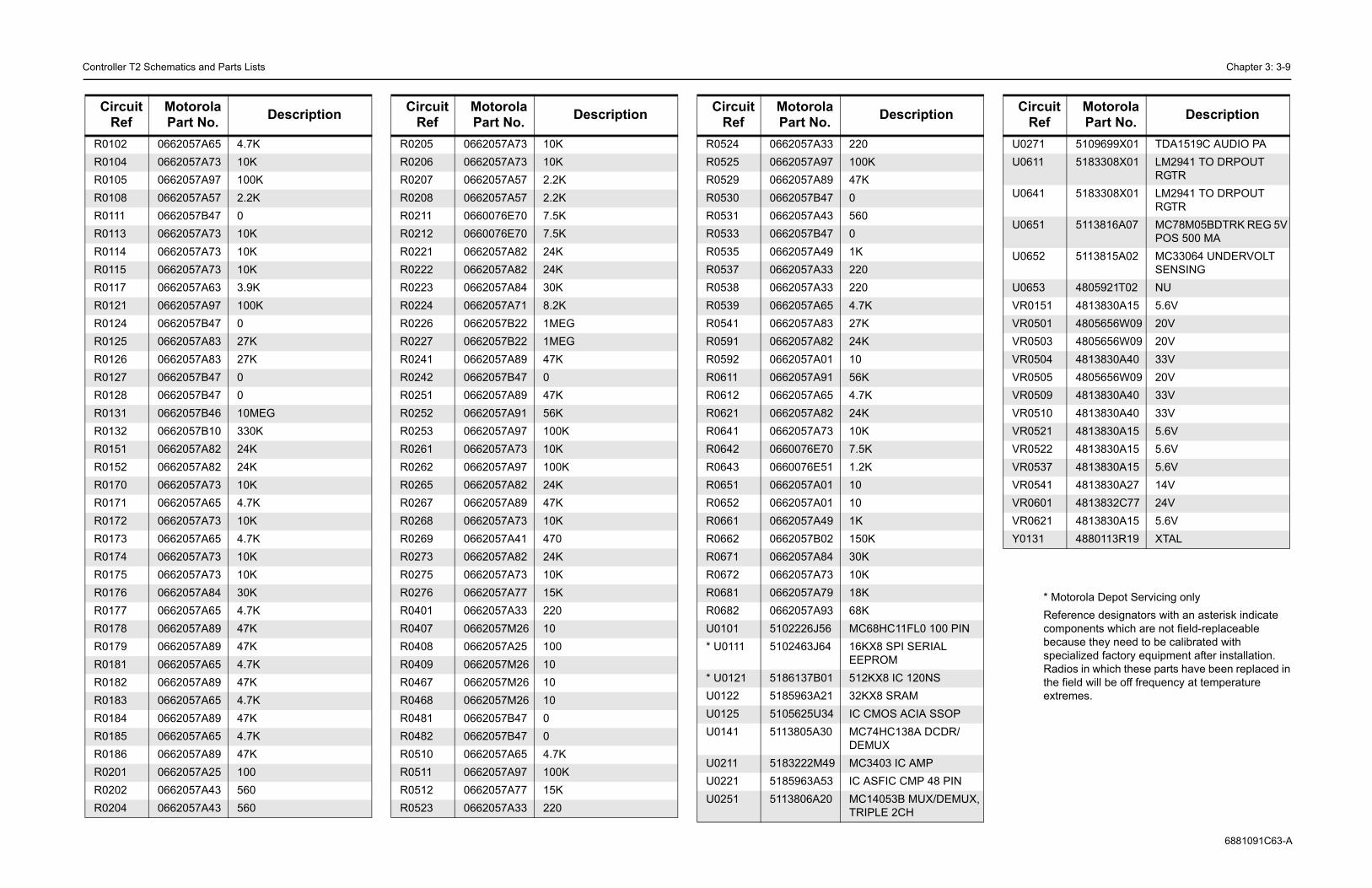
C Chapter 3: 3-9
6881091C63-A
* Motorola Depot Servicing onlyReference designators with an asterisk indicate components which are not field-replaceable because they need to be calibrated with specialized factory equipment after installation. Radios in which these parts have been replaced in the field will be off frequency at temperature extremes.
220100K47K056001K2202204.7K27K24K1056K4.7K24K10K7.5K1.2K10101K150K30K10K18K68KMC68HC11FL0 100 PIN16KX8 SPI SERIAL EEPROM512KX8 IC 120NS32KX8 SRAMIC CMOS ACIA SSOPMC74HC138A DCDR/DEMUXMC3403 IC AMPIC ASFIC CMP 48 PINMC14053B MUX/DEMUX, TRIPLE 2CH
Description
U0271 5109699X01 TDA1519C AUDIO PAU0611 5183308X01 LM2941 TO DRPOUT
RGTRU0641 5183308X01 LM2941 TO DRPOUT
RGTRU0651 5113816A07 MC78M05BDTRK REG 5V
POS 500 MAU0652 5113815A02 MC33064 UNDERVOLT
SENSINGU0653 4805921T02 NUVR0151 4813830A15 5.6VVR0501 4805656W09 20VVR0503 4805656W09 20VVR0504 4813830A40 33VVR0505 4805656W09 20VVR0509 4813830A40 33VVR0510 4813830A40 33VVR0521 4813830A15 5.6VVR0522 4813830A15 5.6VVR0537 4813830A15 5.6VVR0541 4813830A27 14VVR0601 4813832C77 24VVR0621 4813830A15 5.6VY0131 4880113R19 XTAL
Circuit Ref
Motorola Part No. Description
ontroller T2 Schematics and Parts Lists
R0102 0662057A65 4.7KR0104 0662057A73 10KR0105 0662057A97 100K R0108 0662057A57 2.2KR0111 0662057B47 0 R0113 0662057A73 10KR0114 0662057A73 10KR0115 0662057A73 10KR0117 0662057A63 3.9KR0121 0662057A97 100KR0124 0662057B47 0 R0125 0662057A83 27KR0126 0662057A83 27KR0127 0662057B47 0 R0128 0662057B47 0 R0131 0662057B46 10MEGR0132 0662057B10 330KR0151 0662057A82 24KR0152 0662057A82 24KR0170 0662057A73 10KR0171 0662057A65 4.7KR0172 0662057A73 10KR0173 0662057A65 4.7KR0174 0662057A73 10KR0175 0662057A73 10KR0176 0662057A84 30KR0177 0662057A65 4.7KR0178 0662057A89 47KR0179 0662057A89 47KR0181 0662057A65 4.7KR0182 0662057A89 47KR0183 0662057A65 4.7KR0184 0662057A89 47KR0185 0662057A65 4.7KR0186 0662057A89 47KR0201 0662057A25 100R0202 0662057A43 560R0204 0662057A43 560
Circuit Ref
Motorola Part No. Description
R0205 0662057A73 10KR0206 0662057A73 10KR0207 0662057A57 2.2KR0208 0662057A57 2.2KR0211 0660076E70 7.5KR0212 0660076E70 7.5KR0221 0662057A82 24KR0222 0662057A82 24KR0223 0662057A84 30KR0224 0662057A71 8.2KR0226 0662057B22 1MEGR0227 0662057B22 1MEGR0241 0662057A89 47KR0242 0662057B47 0 R0251 0662057A89 47KR0252 0662057A91 56KR0253 0662057A97 100KR0261 0662057A73 10KR0262 0662057A97 100KR0265 0662057A82 24KR0267 0662057A89 47KR0268 0662057A73 10KR0269 0662057A41 470R0273 0662057A82 24KR0275 0662057A73 10KR0276 0662057A77 15KR0401 0662057A33 220R0407 0662057M26 10R0408 0662057A25 100R0409 0662057M26 10R0467 0662057M26 10R0468 0662057M26 10R0481 0662057B47 0R0482 0662057B47 0R0510 0662057A65 4.7KR0511 0662057A97 100KR0512 0662057A77 15KR0523 0662057A33 220
Circuit Ref
Motorola Part No. Description
R0524 0662057A33R0525 0662057A97R0529 0662057A89R0530 0662057B47R0531 0662057A43R0533 0662057B47R0535 0662057A49R0537 0662057A33R0538 0662057A33R0539 0662057A65R0541 0662057A83R0591 0662057A82R0592 0662057A01R0611 0662057A91R0612 0662057A65R0621 0662057A82R0641 0662057A73R0642 0660076E70R0643 0660076E51R0651 0662057A01R0652 0662057A01R0661 0662057A49R0662 0662057B02R0671 0662057A84R0672 0662057A73R0681 0662057A79R0682 0662057A93U0101 5102226J56* U0111 5102463J64
* U0121 5186137B01U0122 5185963A21U0125 5105625U34U0141 5113805A30
U0211 5183222M49U0221 5185963A53U0251 5113806A20
Circuit Ref
Motorola Part No.
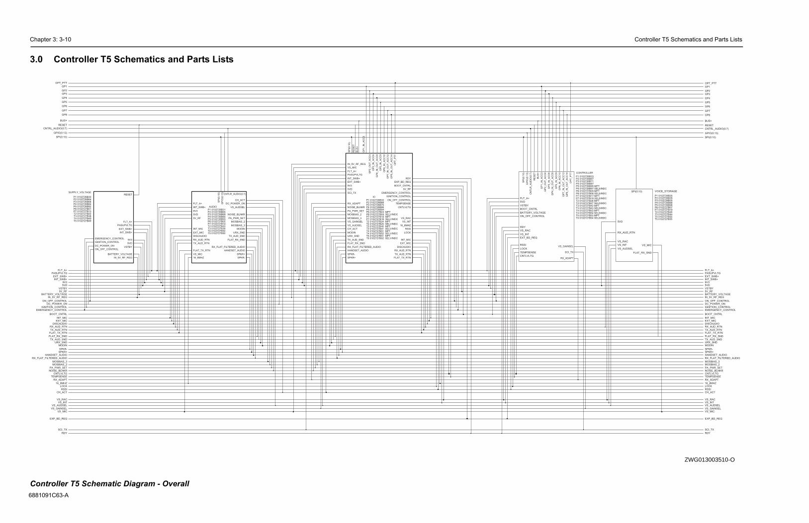
Chapter 3: 3-10 Controller T5 Schematics and Parts Lists
6881091
3.0
T5 0102727B54 SEL5/MDCT5 0102727B53 MPT
T5 0102727B55
P7 0102727B17 MPTP7 0102727B18 SEL5/MDC
P6 0102727B07
P1 0102726B33
P4 0102726B88
P4 0102726B87
P6 0102727B05 MPTP6 0102727B06 SEL5/MDC
P5 0102726B97 SEL5/MDC
P5 0102726B96
P5 0102726B95 MPT
T2 0102727B26 MPT
T2 0102727B28P7 0102727B19
T3 0102727B43 SEL5/MDC
P3 0102726B35P2 0102726B35
T2 0102727B27 SEL5/MDCT3 0102727B42 MPT
T3 0102727B44
P3 0102726B71
P1 0102726B35
P2 0102726B67
T4 0102727B54 SEL5/MDCT4 0102727B53 MPT
T4 0102727B55
TEMPSENSE
VSTBY
VS_GAINSEL
VS_INT
VS_RAC
VOICE_STORAGE
5VD
FLAT_RX_SND
RX_AUD_RTN
SPI(0:10)
VS_AUDSEL
VS_INT VS_MIC
VS_RAC
GP
3_
IN_
AC
C6
GP
4_
IN_
OU
T_
AC
C8
GP
5_
IN_
AC
C9
GP
6_
IN_
AC
C1
0
GP
7_
IN_
OU
T_
AC
C1
2
GP
8_
IN_
OU
T_
AC
C1
4
GP
IO(0
:13
)
LOCK
ON_OFF_CONTROL
OP
T_
PT
T
RDY
RE
SE
T
RSSI
RX_ADAPT
SCI_TX
SP
I(0
:10
) CONTROLLER
5VD
BATTERY_VOLTAGE
BOOT_CNTRL
BU
S+
CN
TL
R_
AU
DIO
(0:7
)
CNTLVLTG
EXT_BD_REQ
FLT_A+
GP
1_
IN_
AC
C3
GP
2_
OU
T_
AC
C4
EXT_SWB+
PASUPVLTGFLT_A+
OPT_PTT
CH_ACT
URX_SND
VS_GAINSEL
MOSBIAS_3
INT_SWB+
EXT_MIC
IN_5V_RF_REGIN
SCI_TX
VS_MIC
5VD9V3
HANDSET_AUDIOHANSPKR+SPKR-
EMERGENCY_CONTROLEMERGENCIGNITION_CONTROLIGNITIO
DC_POWER_ONDCON_OFF_CONTROLON_OF
BATTERY_VOLTAGEBATTER
VSTBY
RDY
P
MOSBIAS_2
MODIN
TX_AUD_SNDT
FLAT_RX_SNDF
16_8MHZ
TX_AUD_RTNTFLAT_TX_RTNF
RX_AUD_RTNRDISCAUDIO
INT_MIC
5V_RF
RX_FLAT_FILTERED_AUDIORX_FLAT_FILTE
GP1
E EXP_BD_REQ
BOOT_CNTRLB
VS_AUDSEL
TEMPSENSECNTLVLTG
VS_RACVS_INT
RSSI
LOCK
RX_ADAPT
NOISE_BLNKRNPA_PWR_SET
CNTRL_AUDIO(0:7)CNTR
GPIO(0:13)
SPI(0:10)
BUS+
RESET
GP8
GP7
GP6
GP5
GP4
GP3
GP2
ZWG013003510-O
Contr
C63-AController T5 Schematics and Parts Lists
T5 0102727B49
T5 0102727B50T5 0102727B51 MPTT5 0102727B52 SELV/MDC
T3 0102727B39T3 0102727B40 MPT
P7 0102727B13
P7 0102727B14
P6 0102727B04 SELV/MDCP6 0102727B03 MPT
P1 0102726B32
P6 0102727B02T2 0102727B25 SELV/MDC
P6 0102727B01
P3 0102726B68
P2 0102726B65
P1 0102726B30
P5 0102726B94
P5 0102726B93
T3 0102727B41 SELV/MDC
P4 0102726B86
P4 0102726B85
P4 0102726B84
T2 0102727B22
T2 0102727B23
T2 0102727B24 MPT
T3 0102727B38
IN_5V_RF_REG
ON_OFF_CONTROL
PASUPVLTG
RESET
VSTBY
P2 0102726B64
P2 0102726B66P3 0102726B70
P3 0102726B69
P1 0102726B31
P7 0102727B16 SELV/MDCP7 0102727B15 MPT
T4 0102727B50
T4 0102727B49
T4 0102727B51 MPTT4 0102727B52 SELV/MDC
P5 0102726B92
TX_AUD_SND
URX_SND
VS_AUDSEL
VS_GAINSEL VS_INT
VS_MIC
VS_RAC
SUPPLY_VOLTAGE
5VD
9V3
BATTERY_VOLTAGE
DC_POWER_ON
EMERGENCY_CONTROL
EXT_SWB+
FLT_A+
IGNITION_CONTROL
INT_SWB+
ON_OFF_CONTROL
OP
T_
PT
T
PASUPVLTG
PA_PWR_SET
RDY
RE
SE
T
RSSI
RX_ADAPT
RX_AUD_RTN
RX_FLAT_FILTERED_AUDIO
SCI_TX
SP
I(0
:10
)
SPKR+
SPKR-
TEMPSENSE
TX_AUD_RTN
GP
3_
IN_
AC
C6
GP
4_
IN_
OU
T_
AC
C8
GP
5_
IN_
AC
C9
GP
6_
IN_
AC
C1
0
GP
7_
IN_
OU
T_
AC
C1
2
GP
8_
IN_
OU
T_
AC
C1
4
HANDSET_AUDIO
IGNITION_CONTROL
INT_MIC
INT_SWB+
IN_5V_RF_REG
LOCKMODIN
MOSBIAS_2
MOSBIAS_3
NOISE_BLNKR
5V_RF
9V3 BOOT_CNTRL
BU
S+
CH_ACT
CNTLVLTG
DISCAUDIO
EMERGENCY_CONTROL
EXP_BD_REQ
EXT_MIC
EXT_SWB+
FLAT_RX_SND
FLAT_TX_RTN
FLT_A+
GP
1_
IN_
AC
C3
GP
2_
OU
T_
AC
C4
IO
16_8MHZ
5VD
TX_AUD_RTN
TX_AUD_SND
URX_SND
VS_AUDSEL
VS_MIC
FLAT_TX_RTN
FLT_A+ GP
IO(0
:13
)
HANDSET_AUDIO
INT_MIC
INT_SWB+
MODIN
MOSBIAS_2
MOSBIAS_3
NOISE_BLNKR
PA_PWR_SET
RX_AUD_RTN
RX_FLAT_FILTERED_AUDIO
SP
I(0
:10
)
SPKR+
SPKR-
EXT_SWB+
PASUPVLTGFLT_A+
AUDIO
16_8MHZ
5VD
5V_RF
9V3
CH_ACT
CNTLR_AUDIO(0:7)
DC_POWER_ON
DISCAUDIO
EXT_MIC
FLAT_RX_SND
OPT_PTT
CH_ACT
URX_SND
VS_GAINSEL
MOSBIAS_3
INT_SWB+
EXT_MIC
_5V_RF_REG
SCI_TX
VS_MIC
5VD9V3
DSET_AUDIOSPKR+SPKR-
Y_CONTROLN_CONTROL
_POWER_ONF_CONTROL
Y_VOLTAGE
VSTBY
RDY
A_PWR_SET
MOSBIAS_2
MODIN
X_AUD_SND
LAT_RX_SND
16_8MHZ
X_AUD_RTNLAT_TX_RTN
X_AUD_RTNDISCAUDIO
INT_MIC
5V_RF
RED_AUDIO
GP1
XP_BD_REQ
OOT_CNTRL
VS_AUDSEL
TEMPSENSECNTLVLTG
VS_RACVS_INT
RSSI
LOCK
RX_ADAPT
OISE_BLNKR
L_AUDIO(0:7)
GPIO(0:13)
SPI(0:10)
BUS+
RESET
GP8
GP7
GP6
GP5
GP4
GP3
GP2
oller T5 Schematic Diagram - Overall

Controller T5 Schematics and Parts Lists Chapter 3: 3-11
6881091C63-A
0.1uFC0681
24K
R0621
GND
3
INPUT2
RESET_1
C0654
U0653
MC33464N-45ATR
10uF
U0651MC78M05
GN
D
2
IN1 3
OUT
0.1uFC0655
NU5.6VVR0671
Q0681
68KR0682
18KR0681
33uFC0652
U
651uF
470pFC0621 C0622
47uFNU
R0671
R0672
30K
10K 0.1uFC0671
D0621
VR0621
6NC3
7NC4
NC5 8
1RESET
5.6V
MC33064U0652
4
GN
D
2INPUT
3NC1
5NC2
9V3
FLT_A+
IN_5V_RF_REG
RESET
5VD
NU
BATTERY_VOLTAGE
EXT_SWB+
INT_SWB+
PASUPVLTG
VSTBY
6VDC
5VDC
5VDC (0VDC during reset)
5VDC
Controller T5 Schematic Diagram - Supply Voltage
47K
47K
47K
47K
470pF
C066147uF
C0601
R06427.5K 33uF
C0641470pF
C0644
J0601-2
C06120.1uF
R0641
J0601-1
10K
R0662
C0662.01uF
150K
D0660
R0652
10Q0641
TP0661
C06630.1uF
R06431.2K
D0651
Q0661
R061156K
E063157R01
22uFC0611
10
R0651
0.1uF
N
C00.1
C0645
24VVR0601
6
GND2
2ON_OFF
VIN4
VOUT5
LM2941
U0641
ADJ1
3
GND1
4.7KR0612
D0661
Q0662
3
GND1
6
GND2
ON_OFF2
4 VIN5VOUT
U0611
LM2941
1ADJ
J0601-3
Q0663
C060310uF
R0661
1K
DC_POWER_ON
IGNITION_CONTROL
EMERGENCY_CONTROL
ON_OFF_CONTROL
0V (13,8VDC when radio off)
ZWG013030506-O
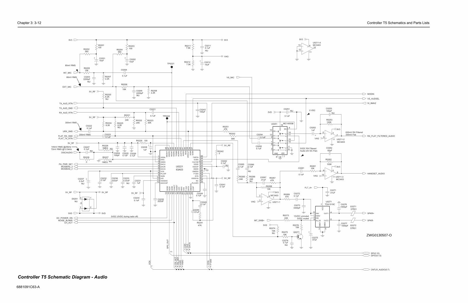
Chapter 3: 3-12 Controller T5 Schematics and Parts Lists
6881091
0269470
144
11
MC3403
U0211-4
13
12
C0272
0.1uF
3300pF
C0273
100K
R0253
C0253
100pF
1uF
NU
C0252
M_SS8
NINV1
OUT14
OUT26
3RR
VC
C
7 TDA1519C
GN
D1
2 5
GN
D2
INV9
U0271
1uF
NU
274
K
75 Q0271
C0261
0.1uF
MC3403
U0211-3
9
10
84
11
MC3403
U0211-2
6
57
4
11
47uFC0275
273
4K
1000pFC0277
E0272
57R01
57R01
E0271
10K
C0262
82pF
R0261
15KR0276
C0276
1000pF
0251
.1uF
NU
.01uF
C0271
15Y
4Z
10B
9C
6N
14X
C14053B
A11
R0262
100K
9V3
9V3
9V3
MODIN
16_8MHZ
SPKR-
FLT_A+
SPKR+
VS_AUDSEL
SPI(0:10)GPIO(0:13)
CNTLR_AUDIO(0:7)
VAG
VAG
HANDSET_AUDIO
RX_FLAT_FILTERED_AUDIO
13VDC unmuted5VDC muted
5VDC RX FilteredAudio (0V DC Flat)
630mV RX Filtered330mV Flat
0 VDC
ZWG0130507-O
Contr
C63-A
CH
_A
CT
SQ
_D
ET
LS
IO
F1200
SY
N
CL
K
HS
IO
VO
X
GP
2_O
UT
CS
X
DA
TA
R0251
47K
24KR0222
C0222
0.1uF
C02260.1uF
R
9
NU
R02208.2K
R02258.2K
R02248.2K
NU
0
C0243100pF
R0242
NU0.1uFC0242
10uFC0202
R0203100
0.1uF
C0265
D0201 5
3
1
2
4
0.1uF
NU
C0254
C0234
0.1uF
7
C02250.1uF
0.C0
C02320.1uF
1MEG
R0227
100
NU
R0229
C02440.1uF
.022uF
C0212
C0235
10uF
NU1MEG
R0226
5
1uF
C0228
10
R02
R0228
0
C0221
0.1uF
0.1uF
C0223
56K
R0252
R02127.5K
R02117.5K
.033uFC0236
8
10uFC0201
11
R0
2
4
R0206
C020510K
NU2200pF
R0266
NU
C02660.1uF
NU24K
C0267
.01uF
0.1uFC0245
C02410.1uF
R0207
TP0221
14
11
2.2K
MC3403
U0211-1
2
3
0.1uFC0227
10K
NUC0224
NU
R0274
100pF
NU
0.22uFC0233
2.2uFC0237
47K
NU
10K
R0267R0265
R0268
24K
45
VD
DR
C
27VDDSYN
7VOX
1
36TXRTN
44
TX
SN
D10
UIO
39
UR
XO
UT
1VDDA
32VDDCP
33VDDD
11VDDDAC
46
MIC
INT
40
MO
D
26NC
8PLCAP
25PLCAP2
17
SQ
DE
T9
SQIN28
SYN
31GNDD
30GNDD0
47
GN
DR
C
23
GN
DS
YN
19
HS
IO
LC
AP
24
18
LS
IO
48
MIC
EX
T
29F1200
15
GC
B0
14
GC
B1
13
GC
B2
35GCB3
GC
B4
37
38
GC
B5
3GNDA
21
CL
K
34CLK168
20
CS
X
6DACG
5DACR
DACU4
22
DA
TA
2DISC
12AGCCAP
41
AU
DIO
AU
XR
X4
3
42
AU
XT
X
16
CH
AC
T
6
U0221
63A53
2.2KR0208
0.1uFC0211
R0204NU
560
R0202560
100R0201
R020510K
R022330K
TP0222
1uFC0231
7
2
C
0
3
0.1uFC0255
R0241
47K
.01uFC0246
13X1
2Y0
1Y1
5Z0
Z13
E
8
GND
16
VC
C
7
VEE
12X0
U0251 M
C02032200pF
0.1uF
NU
C0204
R0221
24K
5VD
5V_RF5V_RF5V_RF
TX_AUD_RTN
5V_RF
TX_AUD_SND
5V_RF
DISCAUDIO
5V_RF
INT_SWB+CH_ACT
VAG
9V3 9V3
9V3
VS_MIC
MOSBIAS_3
VAG
EXT_MIC
5V_RF
5V_RF
5VD
RX_AUD_RTN
INT_MIC
URX_SND
FLAT_RX_SND
DC_POWER_ON
5VD
5VD
PA_PWR_SET
MOSBIAS_2
FLAT_TX_RTN
NOISE_BLNKR
80mV RMS
80mV RMS
5VDC (0VDC during radio off)
300mV RMS
200mV RMS
145mV RMS @25kHz72mV RMS @12.5kHz
oller T5 Schematic Diagram - Audio
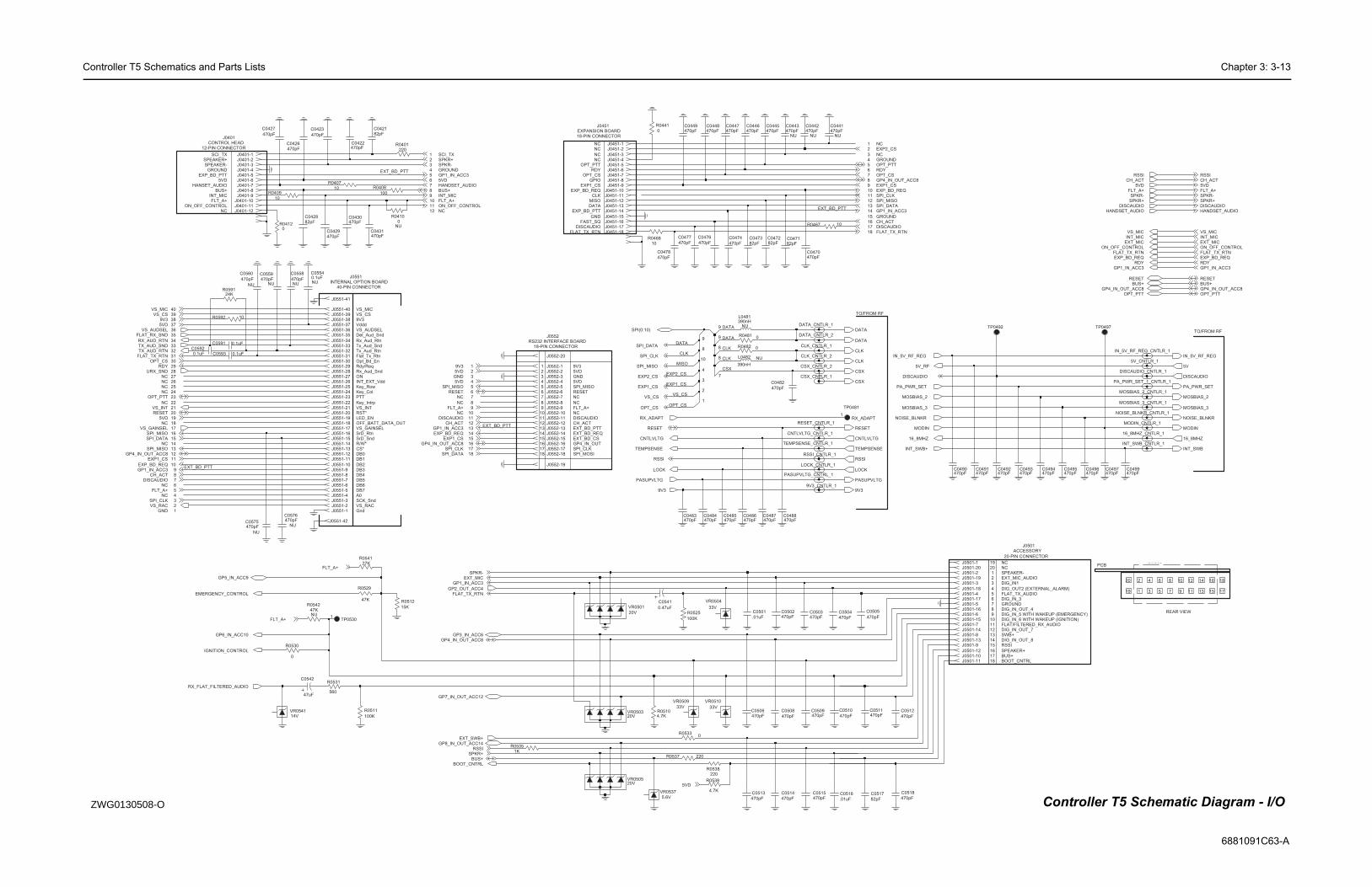
Controller T5 Schematics and Parts Lists Chapter 3: 3-13
6881091C63-A
NC
14
7
9
6
PCB
17
GROUND
5
DIG_IN_5 WITH WAKEUP (EMERGENCY)
13DIG_IN_OUT_7
2 8
BOOT_CNTRL
RX_ADAPT
1
DIG_IN_3
8
DIG_IN_OUT_4
GM300
SPEAKER-
13
6
ACCESSORY
16
19
FLAT_TX_AUDIO
13
10
12
11
16
14
WARIS
TO/FROM RF
7
1
DIG_OUT2 (EXTERNAL_ALARM)
NC
20-PIN CONNECTOR
J0501
DIG_IN_6 WITH WAKEUP (IGNITION)FLAT/FILTERED_RX_AUDIO
9
7
4
11
9
4
18
RSSI
NC
GROUND
DIG_IN1
3
EXT_MIC_AUDIO
_PTT
19
12
NC
12
1817
20
SPEAKER+BUS+
15 17
15
DIG_IN_OUT_8SWB+
20 163
45
11
182
GROUND
10 12 14
REAR VIEW
15
6
TO/FROM RF
8
35
10
DISCAUDIO_CNTLR_1
9V3
INT_SWB_CNTLR_1
CLK
INT_SWB
470pFC0497
DATA
470pFC0491
16_8MHZ
CSX
C0495470pF
C0493470pF
TEMPSENSE
5V_CNTLR_1IN_5V_RF_REG
IN_5V_RF_REG_CNTLR_1
DISCAUDIO
RESET
470pFC0496
C0510
470pF
470pF
C0505
PASUPVLTG
MOSBIAS_2_CNTLR_1
10
0pFNU
441
C0511
470pF
C0512470pF
CLK
MOSBIAS_2
TP0497
470pFC0492
RSSI
MOSBIAS_3_CNTLR_1
1
TP0481
C0504
470pF
CNTLVLTG
5V
MOSBIAS_3
NOISE_BLNKR
LOCK
CSX
MODIN
PA_PWR_SET_1_CNTLR_1
C0490470pF
C0517
82pF 470pF
C0518
470pF
DATA
C0499
PA_PWR_SET
C0494470pF
TP0492
NOISE_BLNKR_CNTLR_1
.01uF
C0516
MODIN_CNTLR_1
16_8MHZ_CNTLR_1
CH_ACT
GP1_IN_ACC3SPI_DATASPI_MISOSPI_CLKEXP_BD_REQEXP1_CSGP4_IN_OUT_ACC8OPT_CSRDYOPT_PTT
EXP2_CS
DISCAUDIO
MODIN
RDY
OPT_PTTOPT_PTT
INT_MIC INT_MIC
SPKR+SPKR+DISCAUDIO DISCAUDIO
HANDSET_AUDIOHANDSET_AUDIO
RSSI RSSI
IN_5V_RF_REG
GP1_IN_ACC3 GP1_IN_ACC3
INT_SWB+
EXP_BD_REQEXP_BD_REQ
CH_ACT CH_ACT
RDY
16_8MHZ
5V_RF
NOISE_BLNKR
MOSBIAS_2
PA_PWR_SET
FLAT_TX_RTN FLAT_TX_RTN
GP4_IN_OUT_ACC8 GP4_IN_OUT_ACC8
DISCAUDIO
MOSBIAS_3
VS_MIC VS_MIC
BUS+ BUS+RESETRESET
ON_OFF_CONTROL ON_OFF_CONTROL
FLAT_TX_RTN
5VD5VDFLT_A+FLT_A+
EXT_MICEXT_MIC
SPKR-SPKR-
J0501-3
J0501-10
J0501-8
J0501-7
J0501-6J0501-15
J0501-5J0501-16
J0501-18
J0501-13
J0501-1
J0501-11
J0501-12
J0501-2J0501-20
J0501-19
J0501-9
J0501-14
J0501-4J0501-17
Controller T5 Schematic Diagram - I/O
RST*
78
INT_EXT_Vdd
NC
A0
EXT_BD_REQEXT_BD_CSGP4_IN_OUTSPI_CLKSPI_MOSI
SPI_MISORESET
FLT_A+
DISCAUDIOCH_ACT
26
FLAT_TX_RTN
CSX29
12-PIN CONNECTOR
13
FAST_SQDISCAUDIO
23
21
GPIO
DATA
EXP1_CS
VS_AUDSEL
SrD_Rtn
37
EXP_BD_PTT
DATA
36
EXP2_CSRx_Aud_SndON
VS_INT
VS_RAC
6
20
SCI_TX
INT_MIC
Tx_Aud_Snd
NC
1011
Key_Row
Key_Intrp
9V3
VS_MIC
5VD
CLK
30
NC
NC
NC
NC
DB6
DB3
DB7
Opt_Bd_En
NC
33
OPT_CS22
18
40-PIN CONNECTOR
DB5
SCK_Snd
35
NC
NC
DATA
VS_GAINSEL
Gnd
DB2
NC
EXT_BD_PTT
GND5VD
EXP_BD_PTT
GND
CLKMISO
GND
SPEAKER+3
21
24
CS*
3NC
NC
HANSET_AUDIO
ON_OFF_CONTROL
J0451
19
VS_CS
R/W*
3938
9
GROUND
DB111
7
17
12
NC
J0552
NC
GROUND
CLK
EXP1_CS
5
9V3
5VD
EXT_BD_PTT
4
VS_CS
DB4
CLK
12
SrD_Snd
EXT_BD
27
Det_Aud_Snd
Rx_Aud_Rtn
MISO
567
8
LED_EN
NC
8
NC
1514
16
RDYOPT_PTT
34
INTERNAL OPTION BOARD
25
3231
4
12
18-PIN CONNECTOR
NC
GND
123
5
9
J0551
28
FLT_A+
6
SPEAKER-
Flat_Tx_Rtn
NC
EXP_BD_REQ
EXT_BD_PTT
EXT_BD_PTT
15161718
4
123
91011121314
DB0
DATA
CONTROL HEAD
NC
10
OPT_CS
NC
Tx_Aud_Rtn
PTT
Vddd
NC
BUS+
5
67
89
1011121314
40
18-PIN CONNECTORRS232 INTERFACE BOARD
Key_Col
OFF_BATT_DATA_OUT
15161718
J0401
4
EXPANSION BOARD
Rdy/Req
0.1uF
LOCK_CNTLR_1
C0591
J0451-10
C0509470pF
0R0412
470pF
C0514
VR050520V
NU
J0451-3
C05540.1uF
J0401-6
C042182pF
470pFC0445
J0451-8
RSSI_CNTLR_1
R0531
560
J0551-13
470pFC0483
470pF
J0401-1
C0446
470pF
C0478
0R0482
0R0481
NU
10R0468
470pFC0443
C0477
2
J0401-9
470pF
C0447470pF
3
J0551-22
J0551-1
J0451-9
20VVR0503
J0401-8
47K
R0529
J0551-41
4
J0401-11
J0451-5
470pFC0431
VR0501
20V
J0551-14
VR0510
33V
J0551-4
9
J0451-12
470pFC0506
J0451-1
C05920.1uF
J0551-21
J0551-24
C0430
C0593 0.1uF
470pF
PASUPVLTG_CNTRL_1
RESET_CNTLR_1
NU
7
L0482
390nH
J0551-18
100K
R0511
CSX_CNTLR_1J0552-3
J0552-8
8
J0552-10J0552-9
J0552-11
J0401-10
J0551-40
82pFC0472
C0484470pF
14VVR0541
R0407
10
J0551-5
TEMPSENSE_CNTLR_1
470pF
J0551-20
C0429
1
R0538220
J0451-6
C0485470pF
R0408
J0451-2
100
C0488
J0551-23
470pF
C0513
470pF
J0551-26
1TP0530
J0552-16
DATA_CNTLR_1
J0552-18J0552-17
J0552-19
R0467
J0401-2
47C0
J0551-15
J0551-19
1KR0535
J0551-42
J0551-25
J0451-13
470pFC0515
J0552-12
J0552-14J0552-13
470pF
J0552-15
C0508
J0401-12
0
R0530
VR0509
33V
9V3_CNTLR_1
NU
8
9
470pF
C0558
470pFC0426
.01uF
C0501
J0451-16
15K
R0512
470pFC0487
4.7KR0510
100K
R0525
CLK_CNTLR_28
J0451-18
J0451-7
C0422
J0401-5
470pF
J0551-31
J0451-15
R0537 220
J0551-38
82pFC0428
DATA_CNTLR_2
C0503
J0552-1
470pF
C0502470pF
VR0504
33V
J0551-9
C0474
J0551-27
470pF
J0551-28
C047182pF
J0551-10
C0575470pF
NU
CSX_CNTLR_2
470pFC0470
R054127K
J0551-2
J0551-16
J0551-35
J0551-30
L0481
NU
J0451-14
390nH
C0448470pF
J0552-6470pF
C0482
J0552-7
J0551-8
C0427
470pF
J0551-36
J0451-17
10
J0551-3
470pFC0486
NU
J0551-29
C0559470pF
C0423
470pF
47uF
C0542
R05330
J0551-37
J0552-20
J0552-4
J0552-2
470pFNU
J0552-5
NU
C0442
0R0410
R0539
4.7K
J0551-39
J0551-33
470pFC0576
NU
J0551-34
R0409
10
VR0537
5.6V
82pFC0473
J0451-4
24KR0591
J0551-17
470pF
CNTLVLTG_CNTLR_1
C0449
J0401-3
J0551-11
47KR0542
NU
470pF
C0560
NU
0.47uF
R0441
C0541
9
0
J0551-6
J0551-32CLK_CNTLR_1
J0551-7
470pF
C0476
J0401-4
J0401-7
R0592 10
220R0401
J0551-12
J0451-11
5VD
SPKR-SPKR+
ON_OFF_CONTROL
EXP_BD_REQGP1_IN_ACC3
SPI_CLKSPI_DATA
SPKR-EXT_MIC
GP1_IN_ACC3
GP2_OUT_ACC4
GP5_IN_ACC9
GP6_IN_ACC10
GP7_IN_OUT_ACC12
GP8_IN_OUT_ACC14
SPKR+
GP3_IN_ACC6GP4_IN_OUT_ACC8
EXP2_CS
9V3
SPI_MISO
FLAT_TX_RTN
CH_ACT
5VD9V3
5VDSPI_MISO
RESET
FLT_A+
DISCAUDIO
GP4_IN_OUT_ACC8EXP1_CS
RDY
OPT_PTT
INT_MIC
HANDSET_AUDIO
BOOT_CNTRL
5VD
BUS+
GP1_IN_ACC3
FLAT_TX_RTN
5VD
GP4_IN_OUT_ACC8EXP1_CS
EXP_BD_REQGP1_IN_ACC3
CH_ACTDISCAUDIO
FLT_A+
SCI_TX
RX_FLAT_FILTERED_AUDIO
EMERGENCY_CONTROL
FLT_A+
RSSI
EXT_SWB+
EXP1_CS
9V3
SPI(0:10)
RX_ADAPT
FLT_A+
SPI_DATA
SPI_CLK
SPI_MISO
VS_CS
OPT_CSRESET
RESET
PASUPVLTG
BUS+
TEMPSENSE
CNTLVLTG
RSSI
LOCK
OPT_CS
SPI_DATA
TX_AUD_RTN
VS_CSVS_MIC
SPI_CLK
FLAT_RX_SND
RX_AUD_RTN
URX_SND
TX_AUD_SND
VS_INT
5VDVS_AUDSEL
VS_GAINSELSPI_MISO
VS_RAC
IGNITION_CONTROL
FLT_A+
ZWG0130508-O
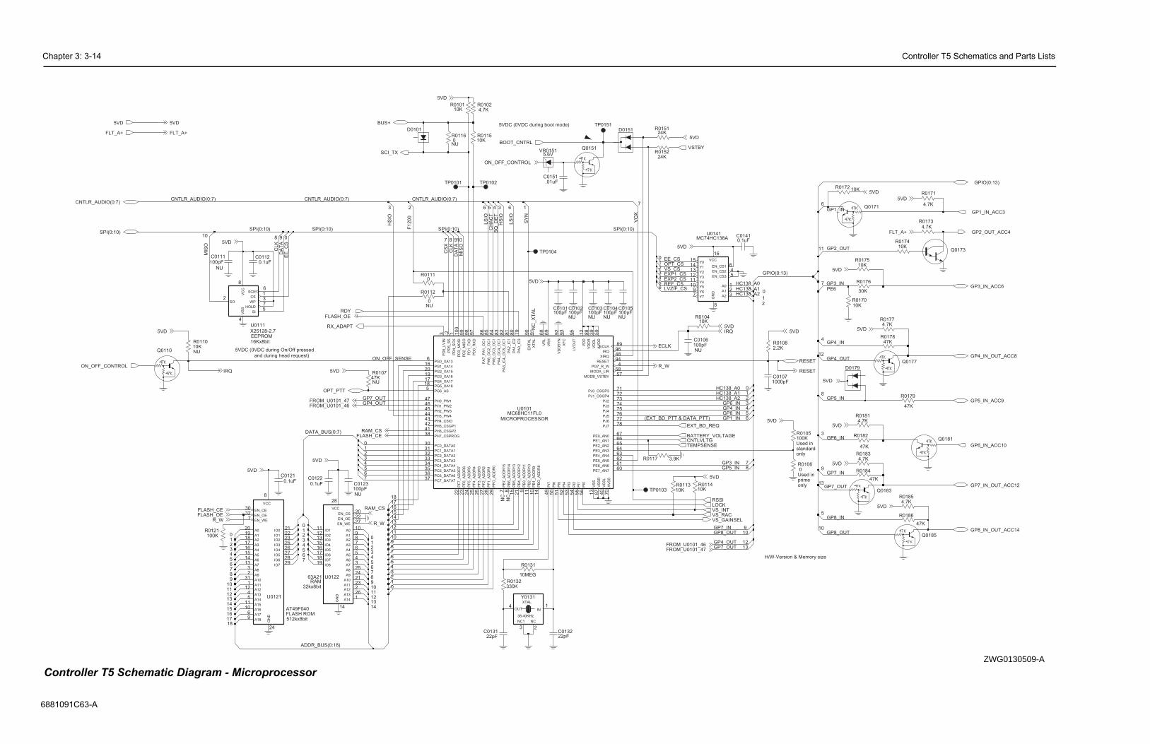
Chapter 3: 3-14 Controller T5 Schematics and Parts Lists
6881091
GP4_IN
GP8_OUT
HC138_A1
GP7_IN
GP5_IN
GP4_OUT
GP7_OUT
TT)
HC138_A0
GP3_IN
GP8_IN
GP6_IN
GP6_IN
GP4_OUTGP7_OUT
HC138_A2
GP1_IN
GP8_OUT
HC138_A1
H/W-Version & Memory size
HC138_A2
GP2_OUT
GP4_IN
GP1_IN
GP5_IN
GP3_IN
GP8_IN
PE6
GP7_IN
HC138_A0
Q0183
5
Q0171
47K
Q0177
R0186
R0176
13
30K
9
R0182
47K
4.7KR0181
R017847K
2
5
7
R01774.7K
R0105
2
4.7K
R0171
4R01082.2K
3
8
R0184
47K
10KR0174
Q0185
Q0173
13
106
10
pF
12
4.7KR0185
6
Q0181
6
9
4
10
R0179
47K
C01410.1uF
7
Y2
Y3
Y4
Y5
Y6
Y7
12
A2 3
EN_CS1 6
EN_CS2 4
EN_CS3 5
GN
D
8
VCC
16
Y0
Y1
U0141C74HC138A
A0 1A1 2
R0172 10K
10KR0175
10
1
1000pFC0107
0K0114
0K104
11
R017010K
R0183
3
4.7K
8
0
4.7K
D0179
R0173
VLTG
5VD
GP1_IN_ACC3
GP6_IN_ACC10
GP2_OUT_ACC4
5VDIRQ
47
VS_RAC
5VD
VS_INT
GP4_IN_OUT_ACC8
GP3_IN_ACC6
5VD
RESET
RESET
5VD
GP5_IN_ACC9
GPIO(0:13)
GPIO(0:13)
46
5VD
5VD
FLT_A+
SENSE
VS_GAINSEL
D_REQ
RSSI
5VD
LOCK
GP7_IN_OUT_ACC12
GP8_IN_OUT_ACC14
5VD
5VD
5VD
5VD
Y
ERY_VOLTAGE100KUsed instandard only
R0106 0Used inprimeonly
ContrZWG0130509-A
C63-A
HS
IO
ON_OFF_SENSE
CH
AC
T
HS
IO
CL
K
32kx8bit
OPT_CS
LVZIF_CS
16Kx8bit
(EXT_BD_PTT & DATA_P
EE_CS
512kx8bit
RAM
MIS
O
EXP2_CS
SQ
_D
ET
FLASH ROM
SY
N
LS
IO
MICROPROCESSOR
DA
TA
MIS
O
F1
20
0
EEPROM
DA
TA
EE
_C
S
VS_CSEXP1_CS
CL
KC
SX
GP4_OUTGP7_OUT
VO
X
LS
IO
REF_CS
VR0151
15
9
7
5.6V
14
TP0104
1514
4
2
R0121100K
10
0
1
0
2
NC
3
NC1
4OUT
1IN
XTAL
Y0131
38.40KHz
0
R0112
NU
4
3
5
8
16
R0131
10MEG
NU
C0111100pF
4.7KR0102
100pFNU
C0103
4
C013122pF
D0101
3.9K
1413
16
R0117
7
5
C0123100pF
C0112
NU
5
0.1uF
2
0
3
Q0151
IO122
IO223
IO325
IO426
IO527
IO628
IO729
8
VCC
A713
A83
A92
EN_CE30
EN_OE32
EN_WE7
24
GN
D
21IO0
A1610
A176
A189
A218
A317
A41615
A514
A6
A020
A119
A1031
A111
A1212
4A13
A145
11A15
3
U0121
AT49F040
6
6
13
4
5
7
R010110K
TP0101
Q0110
47K
18
NU
R0107
10KNU
R0110
9
4
7
109
C0105100pFNU
1
10
8
8
11
6
1
17
10
1
4
5
1
7
TP0151
C0121
0.1uF0.1uF
C0122
18
3
2
TP0103
C013222pF
0
SI5
SO2
VC
C
8
VS
S
4
WP3
U0111
X25128-2.7
CS1
HOLD7
SCK6
.01uFC0151
C0
12
NU100
D0151
65
10
TP0102
6
8
2
12IO2
13IO3
15IO4
16IO5
17IO6
18IO7
19IO8
28
VCC
3A7
25A8
24A9
20EN_CS
22EN_OE
27EN_WE
GN
D
14
11IO1
2A12
26A13
1A14
8A2
7A3
6A4
A554
A6
63A21 U0122
10A0
9A1
A102123
A11
11
6
8
6
VR
L
13
VS
S
40
VS
SL
87
VS
SR
XF
C9
3
48XIRQ
91
XT
AL
77PJ6
78PJ7
94RESET
12
VD
D
39
VD
DL
88
VD
DR
92
VD
DS
YN
69
VR
H
68
PI6
49
PI7
71PJ0_CSGP3
72PJ1_CSGP4
73PJ2
74PJ3
75PJ4
76PJ5
41PH6_CSGP2
38PH7_CSPROG
56
PI0
55
PI1
54
PI2
53
PI3
52
PI4
51
PI5
50
PG6_AS
4PG7_R_W
47PH0_PW1
46PH1_PW2
45PH2_PW3
44PH3_PW4
43PH4_CSIO
42PH5_CSGP1
22
PF
7_
AD
DR
7
29
PF
O_
AD
DR
0
6PG0_XA13
16PG1_XA14
20PG2_XA15
19PG3_XA16
17PG4_XA17
18PG5_XA18
5
61
PE7_AN760
28
PF
1_
AD
DR
1
27
PF
2_
AD
DR
2
26
PF
3_
AD
DR
3
25
PF
4_
AD
DR
4
24
PF
5_
AD
DR
5
23
PF
6_
AD
DR
6
2P
D5
_S
S
PD
6_
LV
IN3
PE0_AN067
PE1_AN166
PE2_AN265
PE3_AN364
PE4_AN463
PE5_AN562
PE6_AN6
PC5_DATA536
PC6_DATA637
PC7_DATA7
97
PD
0_
RX
D
98
PD
1_
TX
D
99
PD
2_
MIS
O
10
0P
D3
_M
OS
I
1P
D4
_S
CK
8P
B6
_A
DD
R1
4
7P
B7
_A
DD
R1
5
14
PB
O_
AD
DR
8
30PC0_DATA0
31PC1_DATA1
32PC2_DATA2
33PC3_DATA3
34PC4_DATA4
35
PA
5_
OC
3_
OC
1
85
PA
6_
OC
2_
OC
1
86
PA
7_
PA
1_
OC
1
10
PB
1_
AD
DR
9
11
PB
2_
AD
DR
10
9P
B3
_A
DD
R1
1
21
PB
4_
AD
DR
12
15
PB
5_
AD
DR
13
LV
OU
T9
5
58MODA_LIR
57MODB_VSTBY
79
PA
0_
IC3
80
PA
1_
IC2
81
PA
2_
IC1
82
PA
3_
IC4
_O
C5
_O
C1
83
PA
4_
OC
4_
OC
1
84
59
AV
DD
70
AV
SS
89ECLK
90
EX
TA
L
96IRQ
U0101MC68HC11FL0
NU100pFC0102
100pFC0104
0
NU
0
7
4
NU
R0116
24KR0152
330KR0132
13121110
97
3
1514
M
12
6
2
7
R011510K
R01110
C0101100pF
9 0
1R
1R0
5
2
1
11
121
10KR0113
3
24KR0151
23
0
13
17
9
3
RAM_CS
BUS+
CNTL
SCI_TX
R_W
FLASH_CEFLASH_OE
IRQ
ADDR_BUS(0:18)
DATA_BUS(0:7)
FROM_U0101_
5VDBOOT_CNTRL
5VD
ON_OFF_CONTROL
R_W
5VD
5VD
5VD
OPT_PTT
5VD
SPI(0:10)SPI(0:10) SPI(0:10) SPI(0:10) SPI(0:10)
CNTLR_AUDIO(0:7) CNTLR_AUDIO(0:7)CNTLR_AUDIO(0:7)CNTLR_AUDIO(0:7)
FROM_U0101_47FROM_U0101_46
FROM_U0101_
TEMP
RAM_CS
5VD
EXT_B
RX_ADAPT
5VD
5VD5VD
FLT_A+ FLT_A+
FLASH_OE
NC
_X
TA
L
ECLK
NC
NC
RDY
ON_OFF_CONTROL
FLASH_CE
R_W
VSTB
5VD
BATT
5VDC (0VDC during On/Off pressed and during head request)
5VDC (0VDC during boot mode)
oller T5 Schematic Diagram - Microprocessor

Controller T5 Schematics and Parts Lists Chapter 3: 3-15
6881091C63-A
0
R0343
uF
INPUT1
OUTPUT
2SENSE
3SHUTDOWN
6VTAP
02
LP2951ACMM-3.3
U0351
5ERROR
7FEEDBACK
4
GN
D
8
R034747K
C0341
1uF
100pFC0303
5.1K
R0345
U0342
CNTL
4
1 2VDD
5
VSS
3
TC4S66F
6
0.1uFC0344
6
5
78
4
LM2904U0341-2
R03421.8K0343
.1uF
R0344
56K
C035333uF
C0352.022uF 0.1uF
C0354
PWR_GND
U0331-2
GND
3
VCC
5
0.1uFC0331
5VD
FLAT_RX_SND
R0341
10K
VS_MIC
3V3
5VD
5VD
VS_AUDSEL
Controller T5 Schematic Diagram - Voice Storage
ZWG0130505-O
5109152M01
VS_CS
MISO
VS_CS
DATA
CLK
0.1
10
C03
0.1uF
0.1uF
2
C0351
C0305
R0323
18K
C0304
0.1uF
1V
SS
A1
17
VS
SA
2
18
VS
SA
3
12
VS
SD
6XCLK
19NC7 21NC8
23NC9
2RAC
8SCLK
9SS
26
VC
CA
7
VC
CD
3NC1
27NC10 28NC11
4NC2
13NC3
14NC4
15NC5
16NC6
AMCAP22
24ANA_NEG
25ANA_POS
20AUDOUT
INT5
11MISO
10MOSI
U0301
U0341-1
LM2904
2
31
8
4
R034
47K
10K
R0331
53
12
4
D0301
R032418K
8
C03420.1uF
C
0
10K
1uFC0301
R0333
C0325
9
0.1uF
150KR0335
U0331-1
74AHCT1G125
A
2
OE 1Y
4
2
R0332
10K
0.1uFC0324
RX_AUD_RTN
3V3
SPI(0:10)
VS_RAC
3V3
5VD
5VD5VD
VS_INT5VD

Chapter 3: 3-16 Controller T5 Schematics and Parts Lists
688109
Contr
CircR
C0101C0107C0112C0121C0122C0131C0132C0141C0151C0201C0202C0204C0212C0221C0222C0223C0224C0225C0226C0228C0231C0232C0234C0235C0236C0241C0243C0244C0245C0246C0252C0254C0255C0261C0262C0265C0267C0271C0272C0273C0275C0276C0277C0301
pF 10%pF 10%pF 10%pF 50VpF 10%pF 10%pF 10%pF 10%pF 10%pF 10%pF 10%pF 10%pF 10%pF 10%pF 10%pF 10%pF 10% 50V
pF 10%pF 10%pF 10%pF 10%pF 10%pF 10%pF 10%pF 50VpF 10%pF 10%pF 50VpF 10%pF 10% 50V
pF 5%pF 10%
CP 470nF 10% 25V CP 47uF 20% 10V
F 16VF 16VF 50VF 50V10uF 50V 20% CP 22uF 20% 35V
F 16V CP 47uF 20% 10V
F 50V CHIP 33 uF 16
F 16V
Description
C0652 2311049A97 TANT CHIP 33 uF 16C0654 2311049A57 TANT CP 10uF 10% 16VC0655 2113743E20 100nF 16VC0661 2311049C05 TANT CP 47uF 10% 16VC0662 2113741F49 10nF 50VC0663 2113743E20 100nF 16VC0671 2113743E20 100nF 16VC0681 2113743E20 100nF 16VD0101 4880236E05 CHIP SCHOTTKYD0151 4813833C02 DUAL SOT MMBD6100D0179 4813833C02 DUAL SOT MMBD6100D0301 4802245J47 SCHOTTKY BARRIER
(RB471E) Voice storage only
D0621 4813833C02 DUAL SOT MMBD6100D0651 4813833C02 DUAL SOT MMBD6100D0660 4813833C02 DUAL SOT MMBD6100 D0661 4813833C02 DUAL SOT MMBD6100E0271 2484657R01 Ferrite BeadE0272 2484657R01 Ferrite BeadE0631 2484657R01 Ferrite BeadJ0401 0902636Y02 CONN FLEX 12 PINJ0451 0902636Y01 CONN FLEX SIDE ENTRYJ0501 0986105B01 CONN SMD 20 PINJ0551 0905505Y04 CONN ZIF HORIZONTALJ0552 0905505Y03 CONN ZIF 18PINJ0601 0986165B01 DC PWR CONNQ0110 4880048M01 NPN DIG 47k/47kQ0151 4880048M01 NPN DIG 47k/47kQ0171 4880048M01 NPN DIG 47k/47kQ0173 4880052M01 NPN DRLNGTN MXTAQ0177 4880048M01 NPN DIG 47k/47kQ0181 4880048M01 NPN DIG 47k/47kQ0183 4880048M01 NPN DIG 47k/47kQ0185 4880048M01 NPN DIG 47k/47kQ0271 4813824A10 NPN 40V .2AQ0641 4880048M01 NPN DIG 47k/47kQ0661 4805921T02 DUAL ROHM FMC2 RHQ0662 4813824A10 NPN 40V .2A B=50-150Q0663 4880048M01 NPN DIG 47k/47kQ0681 4880052M01 NPN DRLNGTN MXTAR0101 0662057A73 10k 1/16W 5%R0102 0662057A65 4700 1/16W 5%R0104 0662057A73 10k 1/16W 5%R0105 0662057A97 100k 1/16W
Voice storage onlyR0106 0662057B47 0 1/16W
Voice storage only
Circuit Ref
Motorola Part No. Description
1C63-A
oller T5 Parts List
uit ef
Motorola Part No. Description
2113740F51 100pF 5% 50V2113741F25 1nF 50V2113743E20 100nF 16V2113743E20 100nF 16V2113743E20 100nF 16V2113740F35 22pF 5% 50V2113740F35 22pF 5% 50V2113743E20 100nF 16V2113741F49 10nF 50V2311049A57 TANT CP 10uF 10% 16V2311049A57 TANT CP 10uF 10% 16V2113743E20 100nF 16V2311049A57 TANT CP 10uF 10% 16V2113743E20 100nF 16V2113743E20 100nF 16V2113743E20 100nF 16V2113740F51 100pF 5% 50V NP02113743E20 100nF 16V2113743E20 100nF 16V2311049A07 TANT CP 1uF 10% 16V2113743B29 1 uF 10% 16V2113743E20 100nF 16V2113743E20 100nF 16V2113743E07 22nF 16V2113743E10 .033uF 10%2113743E20 100nF 16V2113740F51 100pF 5% 50V2113743E20 100nF 16V2113743E20 100nF 16V2113741F49 10nF 50V2311049A07 TANT CP 1uF 10%2113743E20 100nF 16V2113743E20 100nF 16V2113743E20 100nF 16V2113740F49 82pF 5% 50V2113743E20 100nF 16V2113741F49 10nF 50V2113741F49 10nF 50V2113743E20 100nF 16V2113741F37 3.3nF 50V2311049A99 TANT CP 47uF 20% 10V2113741F25 1nF 50V2113741F25 1nF 50V2311049A07 1uF 10% 16V
Voice storage only
C0302 2113743E20 100nF 16VVoice storage only
C0303 2113740F51 100pF 5% 50VVoice storage only
C0304 2113743E20 100nF 16VVoice storage only
C0305 2113743E20 100nF 16VVoice storage only
C0324 2113743E20 100nF 16VVoice storage only
C0331 2113743E20 100nF 16VVoice storage only
C0341 2311049A07 TANT CP 1uF 10% 16VVoice storage only
C0342 2113743E20 100nF 16VVoice storage only
C0343 2113743E20 100nF 16VVoice storage only
C0344 2113743E20 100nF 16VVoice storage only
C0351 2113743E20 100nF 16VVoice storage only
C0352 2113743E07 22nF 16VVoice storage only
C0353 2311049A97 TANT CHIP 33 uF 16Voice storage only
C0354 2113743E20 100nF 16VVoice storage only
C0421 2113743N48 82.0 pF 5%C0422 2113741F17 470pF 50VC0423 2113741F17 470pF 50VC0426 2113743L09 470 pF 10%C0427 2113743L09 470 pF 10%C0428 2113743N48 82.0 pF 5%C0429 2113743L09 470 pF 10%C0430 2113741F17 470pF 50VC0431 2113741F17 470pF 50VC0445 2113743L09 470 pF 10%C0446 2113743L09 470 pF 10%C0447 2113743L09 470 pF 10%C0448 2113743L09 470 pF 10%C0449 2113743L09 470 pF 10%C0470 2113743L09 470 pF 10%C0471 2113743N48 82.0 pF 5%C0472 2113743N48 82.0 pF 5%C0473 2113743N48 82.0 pF 5%C0474 2113743L09 470 pF 10%C0476 2113743L09 470 pF 10%C0477 2113743L09 470 pF 10%
Circuit Ref
Motorola Part No. Description
C0478 2113743L09 470 C0482 2113743L09 470 C0483 2113743L09 470 C0484 2113741F17 470 C0485 2113743L09 470 C0486 2113743L09 470 C0487 2113743L09 470 C0488 2113743L09 470 C0490 2113743L09 470 C0491 2113743L09 470 C0492 2113743L09 470 C0493 2113743L09 470 C0494 2113743L09 470 C0495 2113743L09 470 C0496 2113743L09 470 C0497 2113743L09 470 C0499 2113743L09 470 C0501 2113741F49 10nFC0502 2113743L09 470 C0503 2113743L09 470 C0504 2113743L09 470 C0505 2113743L09 470 C0506 2113743L09 470 C0508 2113743L09 470 C0509 2113743L09 470 C0510 2113741F17 470 C0511 2113743L09 470 C0512 2113743L09 470 C0513 2113741F17 470 C0514 2113743L09 470 C0515 2113743L09 470 C0516 2113741F49 10nFC0517 2113743N48 82.0C0518 2113743L09 470 C0541 2311049A05 TANTC0542 2311049A99 TANTC0591 2113743E20 100nC0592 2113743E20 100nC0593 2113741B69 100nC0601 2113741F17 470pC0603 2380090M24 LYT C0611 2311049C06 TANTC0612 2113743E20 100nC0622 2311049A99 TANTC0641 2113741F17 470pC0644 2311049A97 TANTC0645 2113743E20 100n
Circuit Ref
Motorola Part No.

C Chapter 3: 3-17
6881091C63-A
* Motorola Depot Servicing onlyReference designators with an asterisk indicate components which are not field-replaceable because they need to be calibrated with specialized factory equipment after installation. Radios in which these parts have been replaced in the field will be off frequency at temperature extremes.
100k 1/16W47k 1/16W 5%0 1/16W560 1/16W 5%0 1/16W1k 1/16W220 1/16W 5%220 1/16W 5%4700 1/16W 5%27k 1/16W 5%24K 1/16W 5%10 1/16W 5%56K 1/16W 5%4700 1/16W 5%24K 1/16W 5%10k 1/16W 5%FILM 7500 1 1FILM 1200 1 110 1/16W 5%10 1/16W 5%1k 1/16W 5%150k 1/16W30k 1/16W 5%10k 1/16W 5%18k 1/16W 5%68k 1/16W 5%MICRO PROCESSOR MC68HC1EEPROM X25128-2.7 SO8IC 512KX8 FLASH ROM (AT49BV020)IC 32K x 8 SRAMIC 10F8 DCDR/REMUX 74HC138IC QUAD OPAMP __3403ASFICCMP 0.5MM TQFPMUX/DEMUX,TRIPLE 2-AUDIO PA TDA1519CEEPROM ANALOG ISD33120EIVoice storage onlyBuFFER/DRIVER 74AHCT1G125Voice storage onlyLINEAR IC OP AMPVoice storage onlySNGL ANALOG SWITCHVoice storage only
Description
U0351 5102463J40 REGULATOR, 3.3VVoice storage only
U0611 5183308X01 ADJ VLTG REG LM2941 TO263
U0641 5183308X01 ADJ VLTG REG LM2941 TO263
U0651 5113816A07 REG 5V POS 500MA MC78M05
U0653 5186205B01 MC33464N-45ATR SOT23-5-RB
VR0151 4813830A15 5.6V 5% 225mWVR0501 4805656W09 ZENER QUAD MMQA20VT1VR0503 4805656W09 ZENER QUAD MMQA20VT1VR0504 4813830A40 SOC23 AUTO SDNVR0505 4805656W09 ZENER QUAD MMQA20VT1VR0509 4813830A40 SOC23 AUTO SDNVR0510 4813830A40 SOC23 AUTO SDNVR0537 4813830A15 5.6V 5% 225mWVR0541 4813830A27 14V 5% 225MWVR0601 4813832C77 TRANS SUP. 24V HIGPWRVR0621 4813830A15 DIODE 5.6V 5% 225mWY0131 4880113R19 CRYSTAL 38.4KHZ
Circuit Ref
Motorola Part No. Description
ontroller T5 Schematics and Parts Lists
R0108 0662057A57 2200 1/16W 5%R0111 0662057B47 0 1/16WR0113 0662057A73 10k 1/16W 5%R0114 0662057A73 10k 1/16W 5%R0115 0662057A73 10k 1/16W 5%R0117 0662057A63 3900 1/16W 5%R0121 0662057A97 100k 1/16WR0131 0662057B46 10.0 MEG OHMS 5%R0132 0662057B10 330k 1/16W 5%R0151 0662057A82 24K 1/16W 5%R0152 0662057A82 24K 1/16W 5%R0170 0662057A73 10k 1/16W 5%R0171 0662057A65 4700 1/16W 5%R0172 0662057A73 10k 1/16W 5%R0173 0662057A65 4700 1/16W 5%R0174 0662057A73 10k 1/16W 5%R0175 0662057A73 10k 1/16W 5%R0176 0662057A84 30k 1/16W 5%R0177 0662057A65 4700 1/16W 5%R0178 0662057A89 47k 1/16W 5%R0179 0662057A89 47k 1/16W 5%R0181 0662057A65 4700 1/16W 5%R0182 0662057A89 47k 1/16W 5%R0183 0662057A65 4700 1/16W 5%R0184 0662057A89 47k 1/16W 5%R0185 0662057A65 4700 1/16W 5%R0186 0662057A89 47k 1/16W 5%R0201 0662057A25 100 1/16W 5%R0202 0662057A43 560 1/16W 5%R0203 0662057A25 100 1/16W 5%R0204 0662057A43 560 1/16W 5%R0205 0662057A73 10k 1/16W 5%R0206 0662057A73 10k 1/16W 5%R0207 0662057A57 2200 1/16W 5%R0208 0662057A57 2200 1/16W 5%R0211 0660076E70 FILM 7500R0212 0660076E70 FILM 7500R0221 0662057A82 24K 1/16W 5%R0222 0662057A82 24K 1/16W 5%R0223 0662057A84 30k 1/16W 5%R0224 0662057A71 8200 1/16W 5%R0228 0662057B47 0 1/16WR0229 0662057A25 100 1/16W 5%R0241 0662057A89 47k 1/16W 5%R0242 0662057B47 0 1/16WR0251 0662057A89 47k 1/16W 5%R0252 0662057A91 56K 1/16W 5%
Circuit Ref
Motorola Part No. Description
R0253 0662057A97 100k 1/16WR0261 0662057A73 10k 1/16W 5%R0262 0662057A97 100k 1/16WR0265 0662057A82 24K 1/16W 5%R0267 0662057A89 47k 1/16W 5%R0268 0662057A73 10k 1/16W 5%R0269 0662057A41 470 1/16W 5%R0273 0662057A82 24K 1/16W 5%R0275 0662057A73 10k 1/16W 5%R0276 0662057A77 15k 1/16W 5%R0323 0662057A79 18k 1/16W 5%
Voice storage onlyR0324 0662057A79 18k 1/16W 5%
Voice storage onlyR0331 0662057A73 10k 1/16W 5%
Voice storage onlyR0332 0662057A73 10k 1/16W 5%
Voice storage onlyR0333 0662057A73 10k 1/16W 5%
Voice storage onlyR0335 0662057B02 150k 1/16W
Voice storage onlyR0341 0662057A73 10k 1/16W 5%
Voice storage onlyR0342 0662057A55 1800 1/16W 5%
Voice storage onlyR0343 0662057B47 0 1/16W
Voice storage onlyR0344 0662057A91 56K 1/16W 5%
Voice storage onlyR0345 0662057A66 5100 1/16W 5%
Voice storage onlyR0346 0662057A89 47k 1/16W 5%
Voice storage onlyR0347 0662057A89 47k 1/16W 5%
Voice storage onlyR0401 0662057A33 220 1/16W 5%R0407 0662057M26 10 5%R0408 0662057A25 100 1/16W 5%R0409 0662057M26 10 5%R0412 0662057B47 0 1/16WR0441 0662057B47 0 1/16WR0467 0662057M26 10 5%R0468 0662057M26 10 5%R0481 0662057B47 0 1/16WR0482 0662057B47 0 1/16WR0510 0662057A65 4700 1/16W 5%R0511 0662057A97 100k 1/16WR0512 0662057A77 15k 1/16W 5%
Circuit Ref
Motorola Part No. Description
R0525 0662057A97R0529 0662057A89R0530 0662057B47R0531 0662057A43R0533 0662057B47R0535 0662057A49R0537 0662057A33R0538 0662057A33R0539 0662057A65R0541 0662057A83R0591 0662057A82R0592 0662057A01R0611 0662057A91R0612 0662057A65R0621 0662057A82R0641 0662057A73R0642 0660076E70R0643 0660076E51R0651 0662057A01R0652 0662057A01R0661 0662057A49R0662 0662057B02R0671 0662057A84R0672 0662057A73R0681 0662057A79R0682 0662057A93U0101 5102226J56
* U0111 5102463J64* U0121 5186137B01
U0122 5185963A21U0141 5113805A30
U0211 5183222M49U0221 5185963A53U0251 5113806A20U0271 5109699X01U0301 5109152M01
U0331 5186204B01
U0341 5180932W01
U0342 5105750U28
Circuit Ref
Motorola Part No.
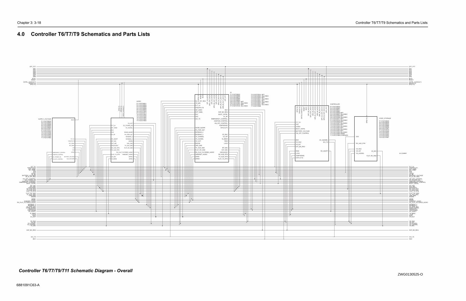
Chapter 3: 3-18 Controller T6/T7/T9 Schematics and Parts Lists
6881091
4.0
T2 0102727B27 SEL5/MDCT3 0102727B42 MPT
T3 0102727B44
P3 0102726B71
P1 0102726B35
P2 0102726B67
T4 0102727B54 SEL5/MDCT4 0102727B53 MPT
T4 0102727B55
P1 0102726B33
P4 0102726B88
P4 0102726B87
P6 0102727B05 MPTP6 0102727B06 SEL5/MDC
P5 0102726B97 SEL5/MDC
P5 0102726B96
P5 0102726B95 MPT
T2 0102727B26 MPT
T2 0102727B28P7 0102727B19
T3 0102727B43 SEL5/MDC
P3 0102726B35P2 0102726B35
T7 0102727B66 STANDARDT7 0102727B65 PRIME
T6 0102727B67
T5 0102727B54 SEL5/MDCT5 0102727B53 MPT
T5 0102727B55
P7 0102727B17 MPTP7 0102727B18 SEL5/MDC
P6 0102727B07
SP
I(0:1
0)
TEMPSENSE
VSTBY
VS_GAINSEL
VS_INT
VS_RAC
VOICE_STORAGE
5VD
FLAT_RX_SND
RX_AUD_RTN
SP
I(0:1
0)
VS_AUDSEL
VS_INT VS_MIC
VS_RAC
GP
2_
OU
T_
AC
C4
GP
3_
IN_
AC
C6
GP
4_
IN_
OU
T_
AC
C8
GP
5_
IN_
AC
C9
GP
6_
IN_
AC
C1
0
GP
7_IN
_O
UT
_A
CC
12
GP
8_IN
_O
UT
_A
CC
14
GP
IO(0
:13)
LOCK
ON_OFF_CONTROL
OP
T_P
TT
RDY
RE
SE
T
RSSI RX_ADAPT
SCI_TX
CONTROLLER
5VD
BATTERY_VOLTAGE
BOOT_CNTRL
BU
S+
CN
TL
R_
AU
DIO
(0:7
)
CNTLVLTG
EXT_BD_REQ
FLT_A+
GP
1_
IN_
AC
C3
PASUPVLTGPAFLT_A+
R RX_ADAPT
CH_ACT
URX_SND
VS VS_GAINSEL
MOSBIAS_3M
I INT_SWB+
EXT_MIC
IN_5V_RF_REGIN_5V
SCI_TX
VS_MIC
5VD9V3
EXT_SWB+E
SPKR+SPKR-
EMERGENCY_CONTROLEMERGENCY_IGNITION_CONTROLIGNITION_DC_POWER_ONDC_POON_OFF_CONTROLON_OFF_
BATTERY_VOLTAGEBATTERY_
VSTBY
RDY
OPT_PTT
MODIN
TX_AUD_SNDTX_FLAT_RX_SNDFLAT
16_8MHZ
TX_AUD_RTNTX_FLAT_TX_RTNFLAT
RX_AUD_RTNRX_DISCAUDIOD
INT_MIC
5V_RF
RX_FLAT_FILTERED_AUDIORX_FLAT_FILTEREHANDSET_AUDIOHANDSE
GP1
EXP EXP_BD_REQ
BOOT_CNTRLBOO
VS VS_AUDSEL
TEMPSENSETECNTLVLTGC
VS_RACVS_INT
RSSILOCK
NOISE_BLNKRNOISPA_PWR_SETPA_MOSBIAS_2M
DUMMY
CNTRL_AUDIO(0:7)CNTRL_AGPIO(0:13)GSPI(0:10)
BUS+RESET
GP8GP7GP6GP5GP4GP3GP2
ContZWG0130525-O
C63-A
Controller T6/T7/T9 Schematics and Parts Lists
T2 0102727B24 MPT
T3 0102727B38
P2 0102726B64
P2 0102726B66P3 0102726B70
P3 0102726B69
P1 0102726B31
P7 0102727B16 SELV/MDCP7 0102727B15 MPT
T4 0102727B50
T4 0102727B49
T4 0102727B51 MPTT4 0102727B52 SELV/MDC
P5 0102726B92
P6 0102727B04 SELV/MDCP6 0102727B03 MPT
P1 0102726B32
P6 0102727B02
T2 0102727B25 SELV/MDC
P6 0102727B01
P3 0102726B68
P2 0102726B65
P1 0102726B30
P5 0102726B94
P5 0102726B93
T3 0102727B41 SELV/MDCP4 0102726B86
P4 0102726B85
P4 0102726B84
T2 0102727B22
T2 0102727B23
INT_SWB+
IN_5V_RF_REGON_OFF_CONTROL
PASUPVLTG
RESET
VSTBY
T7 0102727B62
T7 0102727B63
T7 0102727B68
T5 0102727B49
T5 0102727B50
T5 0102727B51 MPTT5 0102727B52 SELV/MDC
T3 0102727B39
T3 0102727B40 MPT
P7 0102727B13
P7 0102727B14
TX_AUD_SND
URX_SND
VS_AUDSEL
VS_GAINSEL VS_INT
VS_MIC
VS_RAC
SUPPLY_VOLTAGE
5VD
9V3
BATTERY_VOLTAGEDC_POWER_ON
EMERGENCY_CONTROL
EXT_SWB+
FLT_A+
IGNITION_CONTROL
NOISE_BLNKR
ON_OFF_CONTROL
OP
T_P
TT
PASUPVLTG
PA_PWR_SET
RDY
RE
SE
T
RSSI
RX_AUD_RTN
RX_FLAT_FILTERED_AUDIO
SCI_TX
SP
I(0:1
0)
SPKR+
SPKR-
TEMPSENSE
TX_AUD_RTN
GP
2_O
UT
_A
CC
4
GP
3_
IN_
AC
C6
GP
4_
IN_
OU
T_
AC
C8
GP
5_
IN_
AC
C9
GP
6_
IN_
AC
C1
0
GP
7_
IN_
OU
T_
AC
C1
2
GP
8_IN
_O
UT
_A
CC
14
HANDSET_AUDIO
IGNITION_CONTROL
INT_MIC
INT_SWB+
IN_5V_RF_REG
LOCKMODIN
MOSBIAS_2
MOSBIAS_3
5VD 5V_RF
9V3 BOOT_CNTRL
BU
S+
CH_ACT
CNTLVLTG
DISCAUDIO
EMERGENCY_CONTROL
EXP_BD_REQ
EXT_MIC
EXT_SWB+
FLAT_RX_SND
FLAT_TX_RTN
FLT_A+
GP
1_
IN_
AC
C3
IO
16_8MHZ
SPKR+
SPKR-
TX_AUD_RTN
TX_AUD_SND
URX_SND
VS_AUDSEL
VS_MIC
FLAT_RX_SND
FLAT_TX_RTN
FLT_A+
GP
IO(0
:13
)
HANDSET_AUDIO
INT_MIC
INT_SWB+
MODIN
MOSBIAS_2
MOSBIAS_3
NOISE_BLNKR
PA_PWR_SET
RX_ADAPT
RX_AUD_RTN
RX_FLAT_FILTERED_AUDIO
SP
I(0
:10
)
SUPVLTGFLT_A+
X_ADAPT
AUDIO
16_8MHZ
5VD
5V_RF
9V3
CH_ACTC
NT
LR
_A
UD
IO(0
:7)
DC_POWER_ON
DISCAUDIO
EXT_MIC
CH_ACT
URX_SND
_GAINSEL
OSBIAS_3
NT_SWB+
EXT_MIC
_RF_REG
SCI_TX
VS_MIC
5VD9V3
XT_SWB+
SPKR+SPKR-
CONTROLCONTROLWER_ON
CONTROL
VOLTAGE
VSTBY
RDY
OPT_PTT
MODIN
AUD_SND_RX_SND
16_8MHZ
AUD_RTN_TX_RTN
AUD_RTNISCAUDIO
INT_MIC
5V_RF
D_AUDIOT_AUDIO
GP1
_BD_REQ
T_CNTRL
_AUDSEL
MPSENSENTLVLTG
VS_RACVS_INT
RSSILOCK
E_BLNKRPWR_SETOSBIAS_2
UDIO(0:7)PIO(0:13)SPI(0:10)
BUS+RESET
GP8GP7GP6GP5GP4GP3GP2
roller T6/T7/T9/T11 Schematic Diagram - Overall
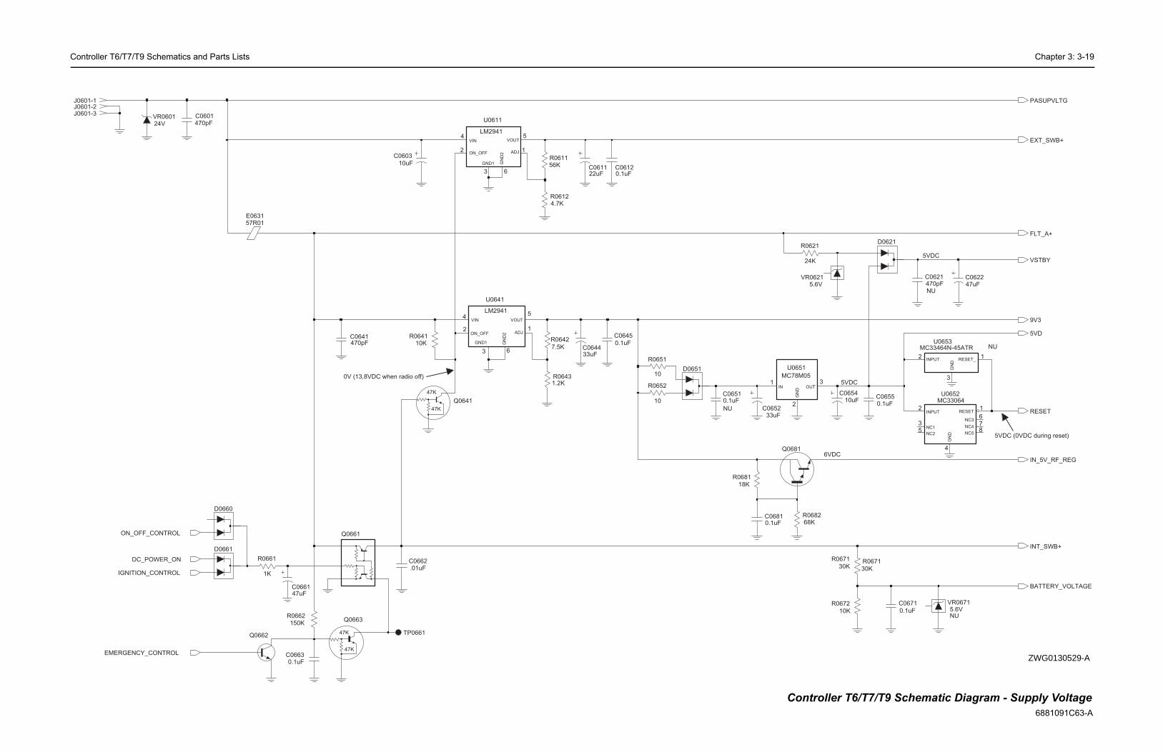
Controller T6/T7/T9 Schematics and Parts Lists Chapter 3: 3-19
6881091C63-A
C0621
NU
2
GN
D
1IN OUT
3
NU
0.1uF
NU
NU
D0621
VR06215.6V
2
NC13
NC25
NC36
NC478
NC5
RESET1
U0652MC33064
GN
D
4
INPUT
MC78M05
U0651
0.1uF
C0651 C0655
470pF 47uFC0622
VR06715.6V
68K
Q0681
R0682
R068118K
C065233uF
R0671
30K
R0671
30K
10K
R06720.1uF
C0671
R0621
24K
2INPUT
1RESET_
MC33464N-45ATRU0653
3
GN
D
C065410uF
C06810.1uF
9V3
FLT_A+
IN_5V_RF_REG
RESET
5VD
BATTERY_VOLTAGE
EXT_SWB+
INT_SWB+
PASUPVLTG
VSTBY
6VDC
5VDC
5VDC (0VDC during reset)
5VDC
ZWG0130529-A
Controller T6/T7/T9 Schematic Diagram - Supply Voltage
47K
47K
47K
47K
TP0661
J0601-3
Q0663
C0603
10uF
R0661
1K
0.1uFC0663
R06431.2K
0.1uF
C0645
24VVR0601
ON_OFF2
4VIN
5VOUT
U0641
LM2941
1ADJ
GND1
3
GN
D2
6
Q0661
R061156K
57R01E0631
22uFC0611
R0651
10
R06124.7K
D0661
Q0662
6
2ON_OFF
VIN4
VOUT5
LM2941
U0611
ADJ 1
GND1
3
GN
D2
10KR0641
C0662
J0601-1
.01uF
R0662150K
D0660
R0652
10Q0641
470pFC0601
C066147uF
R0642
7.5K470pFC0641
33uFC0644
D0651
J0601-2
0.1uFC0612
DC_POWER_ON
IGNITION_CONTROL
EMERGENCY_CONTROL
ON_OFF_CONTROL
0V (13,8VDC when radio off)
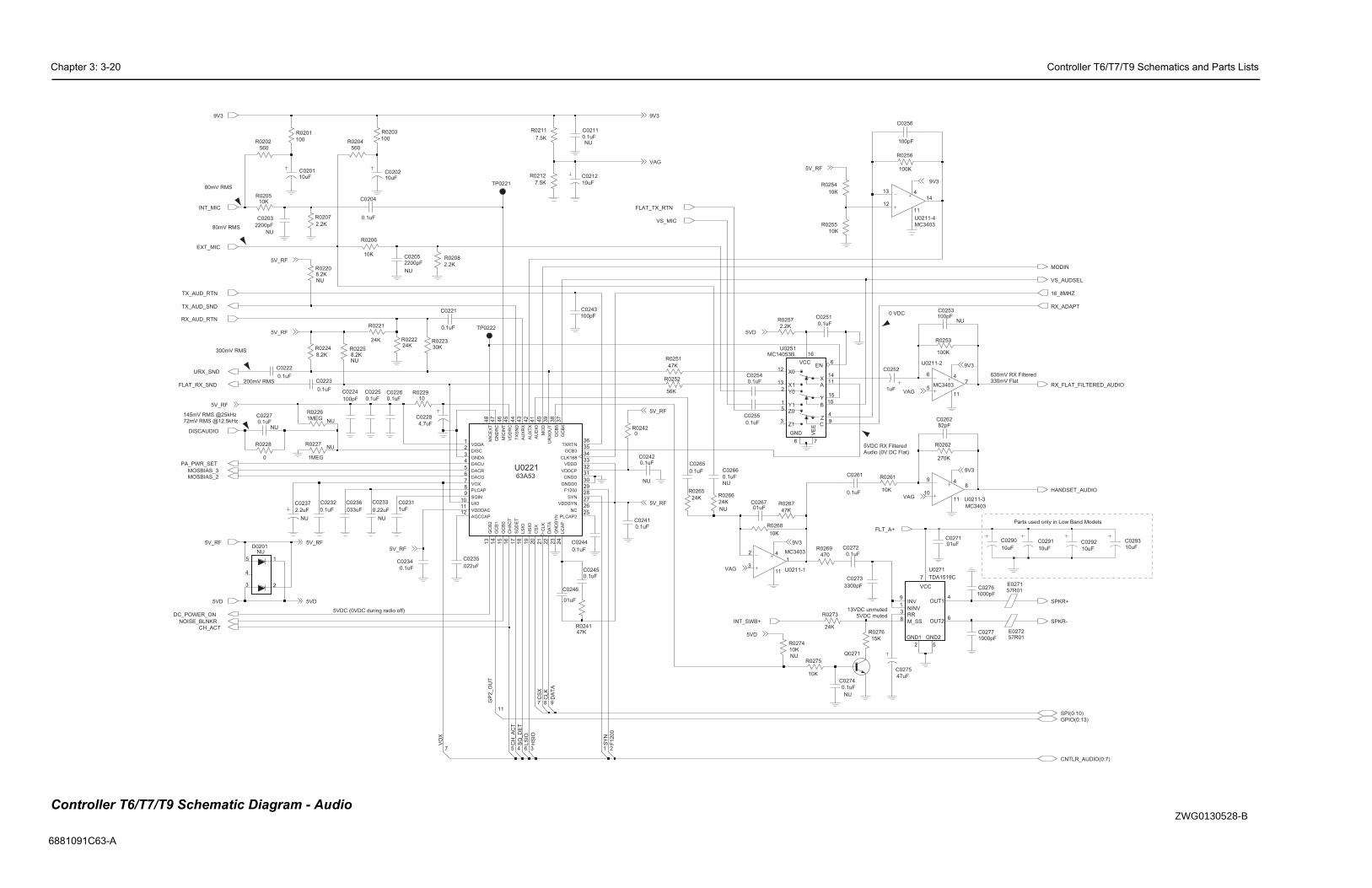
Chapter 3: 3-20 Controller T6/T7/T9 Schematics and Parts Lists
6881091
13VDC unmuted5VDC muted
5VDC RX FilteredAudio (0V DC Flat)
630mV RX Filtered330mV Flat
0 VDC
NU
NU100pFC0253
100pF
C0256
Q0271
0.1uF
C02619
10
84
11 U0211-3
MC3403
VCC
GND2
5
9INV
8 M_SS
1NINV
4OUT1
6OUT2
RR3
7 TDA1519C
U0271
2
GND1
0.1uF
C0274
10K
R0261
82pFC0262
6
57
4
11
U0211-2
MC3403
C0275
47uF
3
100K
R0253
1uF
C0252
K
C02771000pF 57R01
E0272
57R01E0271
15K
1000pF
R0276
C0276
13
1214
4
11
U0211-4
MC3403
C0272
0.1uF
C0273
3300pF
R0262
270K
R0256
100K
C0271.01uF
RX_ADAPT
MODIN
16_8MHZ
SPKR-
FLT_A+
SPKR+
9V3
9V3
9V3
VS_AUDSEL
SPI(0:10)
GPIO(0:13)
CNTLR_AUDIO(0:7)
VAG
VAG
HANDSET_AUDIO
RX_FLAT_FILTERED_AUDIO
Parts used only in Low Band Models
C0291
10uF
C0290
10uF 10uFC0292
10uF
C0293
ContrZWG0130528-B
C63-A
ZWG0130528-B
80mV RMS
80mV RMS
5VDC (0VDC during radio off)
300mV RMS
200mV RMS
145mV RMS @25kHz72mV RMS @12.5kHz
C0204
NU
C0211
C0237
2.2uF
NU
NU
10K
NU
R0274
C0227
NU
R0266
24K
NU0.1uF
C0266
NU
NU
R0227
1MEG
NU0.1uF
C0232
NU
NUD0201
8
C0242
NU
8.2KR0225
NU
NU
NU
SY
N
CL
K
HS
IO
VO
X
GP
2_
OU
T
CS
X
DA
TA
CH
_A
CT
SQ
_D
ET
LS
IO
F1
20
0
TP0222
30KR0223
C0228
4,7uF
R0275
10K
0
R0228
0.1uF
C0221
0.1uF
R0252C0223
56K
7.5K
R0212
7.5K
R0211
.033uF
C0236
47K
R0267
10K
R0268
24K
R0265
VDDDAC11
VD
DR
C4
5VDDSYN
27
VOX7
1
SYN28
TXRTN36T
XS
ND
44
UIO10
UR
XO
UT
39
VDDA1
VDDCP32
VDDD33
MIC
EX
T4
8
MIC
INT
46
MO
D4
0
NC26
PLCAP8
PLCAP225
SQ
DE
T1
7
SQIN9
GNDA3
GNDD31
GNDD030
GN
DR
C4
7
GN
DS
YN
23
HS
IO1
9
LC
AP
24
LS
IO1
8
DISC2
F120029
GC
B0
15
GC
B1
14
GC
B2
13
GCB335
GC
B4
37
GC
B5
38
CH
AC
T1
6
CL
K2
1
CLK16834
CS
X2
0
DACG6
DACR5
DACU4
DA
TA
22
AGCCAP12
AU
DIO
41
AU
XR
X4
3
AU
XT
X4
2
63A53
U0221
C0225
0.1uF
R0208
2.2K
6
0.1uF
560R0204
560
R0202
R0201
R0205
100
5
10K
8.2KR0220
9
8.2K
R0224
100pF
C0243
0R0242
0.1uF
C020110uF
11
24K
R027
4
10
R0255
7
C02052200pF
.01uFC0267
0.1uFC0245
10R0229
0.1uF
C0244
.022uF
C0235
C0212
10uF
R02261MEG
R0206
10K
10K
R0254
1uF
C0231
7
2
10uF
R0203
C0202
0.1uF
100
5
3
1
2
4
C0265
C0254
C0234
0.1uF
0.1uF
24K
R0221 2.2K
R0257
47K
R0251
R022224K
0.1uF
C0222
0.1uFC0226
470
R0269
0.1uF
C0241
TP0221
2.2K
U0211-1
MC34032
31
4
11
R0207
0.1uF
C0224
100pF
C0233
0.22uF
3
0.1uF
C0251
C0255
0.1uF
47KR0241
Z1
C0246
.01uF
14X012
X113
Y15
Y02
Y11
Z4
Z05
3
U0251
11A
B10
C9
EN6
GND
8
VCC
16
VE
E
7
X
MC14053B
2200pF
C0203
TX_AUD_RTN
5V_RF
TX_AUD_SND
5V_RF
DISCAUDIO
5V_RF
FLAT_TX_RTN
5V_RF
0.1uF
INT_SWB+
CH_ACT
VAG
9V3 9V3
9V3
VS_MIC
MOSBIAS_3
VAG
EXT_MIC
5V_RF
5V_RF
5VD5VD
5V_RF
5V_RF5V_RF
RX_AUD_RTN
INT_MIC
URX_SND
FLAT_RX_SND
DC_POWER_ON
5VD
5VD
PA_PWR_SET
MOSBIAS_2
NOISE_BLNKR
oller T6/T7/T9 Schematic Diagram - Audio
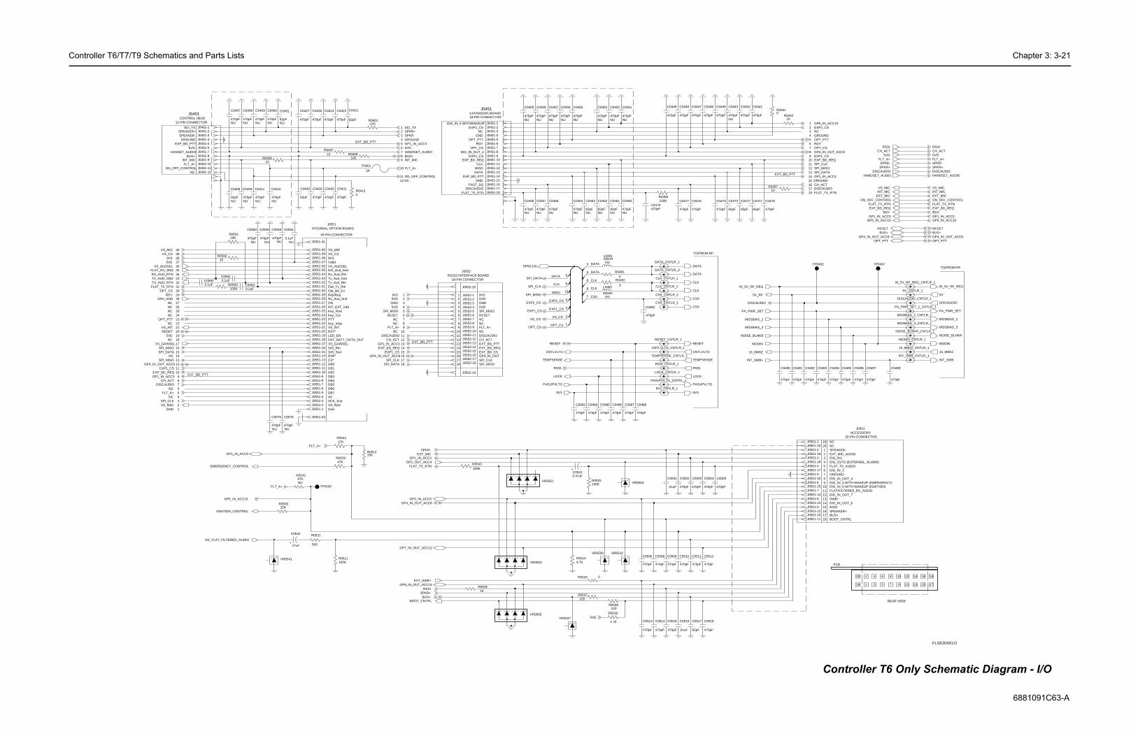
Controller T6/T7/T9 Schematics and Parts Lists Chapter 3: 3-21
6881091C63-A
FLAT/FILTERED_RX_AUDIO
14
REAR VIEW
15
12
SPEAKER+
DIG_OUT2 (EXTERNAL_ALARM)
13DIG_IN_OUT_7
1
4
18
DIG_IN_OUT_8SWB+
20 1610
BOOT_CNTRL
82
5
GROUND
PCB
14
5 15 17
15
6
2
GROUND
6
NC
9
7
BUS+
1
1
10
2
16
DIG_IN_3
8
12
NC
1211
WARIS
TO/FROM RF
7
RSSI
EXT_BD_PTT13
DIG_IN_OUT_4
NC
20
16
6
EXT_MIC_AUDIO
19
19
18
FLAT_TX_AUDIO
10
TO/FROM RF
8
GM300
SPEAKER-
20-PIN CONNECTOR
1817
DIG_IN_6 WITH WAKEUP (IGNITION)
ACCESSORY
34
3 13
J0501
4
11
9
14
11
DIG_IN1
3
17
GROUND
7
9 DIG_IN_5 WITH WAKEUP (EMERGENCY)
5
82pF
C0517
IN_5V_RF_REG_CNTLR_1
MOSBIAS_3
J0501-20
J0501-6
CSX
C0518
470pF
9V3
470pF
C0496
J0501-2
82pF
C0472
TEMPSENSE
5V_CNTLR_1
82pF
C0471
5V
J0501-3
470pF
0511
CLK
C0512
470pF
J0501-12
J0501-11
TP0497
16_8MHZ
J0501-17
16_8MHZ_CNTLR_1
70pF
0503
470pF
C0499
C0470
470pF
1KR0442
J0501-8
DISCAUDIO_CNTLR_1
C0495
470pF470pF
C0492RSSI
MOSBIAS_3_CNTLR_1
R046710
J0501-7
CSX
INT_SWB_CNTLR_1
CLK
INT_SWB
470pFNU
C0443
470pF
J0501-9
C0474
CNTLVLTG
MOSBIAS_2
70pF
0476
TP0492
R04410
J0501-4
0447
70pF
PASUPVLTG
J0501-18
J0501-19
470pF
C0504
MODIN
J0501-14
PA_PWR_SET_1_CNTLR_1
470pF
C0441
J0501-1
RESET
PA_PWR_SET
C0490
470pF
C0493
470pF
DATA
IN_5V_RF_REG
J0501-10
C0445
470pF470pF
C0446
NOISE_BLNKR_CNTLR_1
DISCAUDIO
J0501-5
470pF
C0491
NOISE_BLNKR
LOCK
DATA
MOSBIAS_2_CNTLR_1
470pF
C0494
MODIN_CNTLR_1
C0497
470pF
470pF
C0442
J0501-13
82pF
C0473
470pF
J0501-16
J0501-15
C0505
FLAT_TX_RTN
GP6_IN_ACC10GP6_IN_ACC10
GP6_IN_ACC10
INT_SWB+
DISCAUDIO
MODIN
RDY
OPT_PTT
OPT_PTTOPT_PTT
INT_MIC INT_MIC
SPKR+SPKR+DISCAUDIO DISCAUDIO
HANDSET_AUDIOHANDSET_AUDIO
EXP2_CS
RSSI RSSI
IN_5V_RF_REG
GP1_IN_ACC3
GP1_IN_ACC3 GP1_IN_ACC3
EXP_BD_REQEXP_BD_REQ
CH_ACT CH_ACT
RDY
GP4_IN_OUT_ACC8 GP4_IN_OUT_ACC8
CH_ACT
SPI_DATASPI_MISO
EXP_BD_REQEXP1_CS
OPT_CSRDY
GP4_IN_OUT_ACC8
SPI_CLK
DISCAUDIO
MOSBIAS_3
VS_MIC VS_MIC
16_8MHZ
5V_RF
NOISE_BLNKR
MOSBIAS_2
PA_PWR_SET
FLAT_TX_RTN FLAT_TX_RTN
BUS+ BUS+RESETRESET
ON_OFF_CONTROL ON_OFF_CONTROL
5VD5VDFLT_A+FLT_A+
EXT_MICEXT_MIC
SPKR-SPKR-
FL0830681O
ZWG0130527-B
Controller T6 Only Schematic Diagram - I/O
13
EXT_BD_PTT
EXT_BD_PTT
NC
4
4
RS232 INTERFACE BOARD
18-PIN CONNECTOR
NC
31
DATA
NC
10
5VD
Key_Row
37
CS*
GND
BUS+
5
6789
21
OPT_CS
VS_RAC
6
RST*
78
12
INT_EXT_Vdd
GROUND
GND
5
1514
16
RDY
40
18-PIN CONNECTOR
11
DIG_IN_OUT_4
12
2
SrD_Snd
Flat_Tx_Rtn
NC
1
1011
36
EXP2_CS
NC
17
4
12
EXT_BD_PTT
GND
12
J0401
1718
10
EXT_BD_PTT
13
FAST_SQDISCAUDIO
23
21
38
9
Rx_Aud_Snd
Det_Aud_Snd
MISO
56
GROUND OPT_PTT
34
INTERNAL OPTION BOARD
FLT_A+
SPEAKER-
FLT_A+
DISCAUDIOCH_ACT
NCNC
NC
VS_CS
11
141516
3NC
NC
3
910
EXPANSION BOARD
Rdy/Req
1516
NC5VD
DB3
MISO
GND
20
SCI_TX
39
Tx_Aud_Snd
DB1
22
Rx_Aud_Rtn
SCK_Snd
35
NC
NC
18
8
LED_EN
CLK
9
J0551
28
CONTROL HEAD
6
RESET24
NC
J0552
19
32
EXT_BD_REQEXT_BD_CS
7
17
12
Key_Intrp
9V3
VS_MIC
3
HANSET_AUDIO
11121314
NC
9V3J0552-1J0552-2J0552-3J0552-4J0552-5J0552-6J0552-7J0552-8J0552-9J0552-10J0552-11J0552-12J0552-13J0552-14J0552-15J0552-16J0552-17J0552-18
EXP1_CS
VS_AUDSEL
26
FLAT_TX_RTN
CSX29
INT_MIC
DATA
ON
VS_INT
CLK
EXP_BD_PTT
18
40-PIN CONNECTOR
DB5
SPI_MISO
4
VS_CS
DB4
7
VS_GAINSEL
Gnd
EXP2_CS
8
DB0
DATA
EXP1_CS
5
SrD_Rtn
DIG_IN_6 WITHWAKEUP
CLK
Tx_Aud_Rtn
PTT
Vddd
25
3
33
OPT_CS
GP4_IN_OUTSPI_CLKSPI_MOSI
J0552-19
J0552-20
NC
DATA
ON_OFF_CONTROL
J0451
Opt_Bd_En
Key_Col
EXP_BD_REQ
NC
NC
DB6
5VD
OFF_BATT_DATA_OUT
CLK
30
R/W*
EXP_BD_PTT
SPEAKER+
DB2
27
DB7
GND
A0
12-PIN CONNECTOR
J0551-36
J0401-1
10
CNTLVLTG_CNTLR_1
J0551-3
J0401-12
470pF
C0457
NU
NU
L0481390nH
470pF
C0449
C0430
470pF
J0551-37
RESET_CNTLR_1
PASUPVLTG_CNTRL_1
J0401-2
VR0503
CLK_CNTLR_1
J0451-17
82pFNU
C0461
J0451-3
NU0.1uF
C0554
470pF
C0502
C0453
NU470pF
R05104.7K
J0551-20
C0409
J0451-10
NU470pF
C0509
470pF
J0551-5
J0451-13
470pF
C0515
J0551-25
J0401-11
VR0501
J0551-4
J0551-14
J0551-31
R0412
3A
0470pF
J0451-5
C0431
10R0592
J0551-23
J0551-18
R0511100K
CSX_CNTLR_1
J0401-5
J0551-27
J0451-12
VR0510
9
C0506
470pF
470pF
C0429
J0551-19
R051215K
C0426
470pF
C0501
.01uF
C0468
NU470pF
470pF
C0514
VR0505
J0551-12
J0401-6
J0551-6
J0551-10
NU470pF
C0575470pF
C0487
470pF
C0464
J0551-34
NU
10R0409
J0451-2
C
J0551-42
7
TP0530
J0551-1
J0451-9
J0551-32
DATA_CNTLR_2
4
C
NU
C0462
82pF
C0486
470pF
CSX_CNTLR_2
27KR0541
470pF
C0410
J0451-1
NU
0.1uFC0592
J0551-21
NU470pF
C0403
2
470pF
C0477
LOCK_CNTLR_1
0.1uFC0591
R052947K
J0551-41
470pF
C0456
470pFNU NU
C0455
J0551-9
470pF
470pF
C0427
C0482
J0551-38
82pF
C0428J0451-18
8CLK_CNTLR_2
J0451-7
470pF470pF
C0452C0422
NU470pFNU
C0407
J0451-8
220R0538
J0451-6
1
100KR0543
C0485
470pF
C0478470pF
R0482
0
0
R0468100K
R0481
J0551-28
9
9V3_CNTLR_1
470pF
8
NU
C0558
82pF
C0421
J0451-16
R040710
470pF
C0508
J0551-7
4
C
J0551-33
NU
C0576
470pF
C05410.47uF
9
100
J0551-15
R0408
470pF
C0466
C0408
82pF
NU
J0551-40
NU
DATA_CNTLR_1
NU390nH
L0482
J0551-22
C
4
3
C0488
470pF
470pF
C0513
470pF
1K
NU
C0460
R0535
R0593
VR0504
100K
J0551-8
J0551-2
J0551-16
VR0541
J0401-4
J0401-10J0401-9
J0401-7
J0401-3
J0401-8
470pF
C0423
J0551-29
47uF
C0542
0R0533
J0551-30
J0551-35
J0451-14
J0451-4
24K
J0551-17
R0591
4
R0531
560
82pF
C0463
C0451
NU
NU470pF
82pF
C0401
J0551-24
NU
0.1uFC0593
C0406
NU470pF
C0484
470pF
470pF
C0458C0459
NUNU470pF
R0525100K
J0551-13
470pF
C0483
C0448
470pF
220R0401
J0451-11
J0551-11
470pF
C0467
C0559
NU
NU470pF
C0560
470pFNU
VR0509
C0516
.01uF
RSSI_CNTLR_1
470pFNU
C0411
NU470pF
C0402
F0401
4.7K
R0539
J0551-39
J0551-26
R0537220
J0451-15
47KNU
R0542
VR0537
R053022K
TEMPSENSE_CNTLR_1
C0510
470pF
8
SPKR+
FLT_A+
5VDGP1_IN_ACC3
ON_OFF_CONTROL
EXP1_CSEXP_BD_REQGP1_IN_ACC3
SPI_CLKSPI_DATA
SPKR-EXT_MIC
GP1_IN_ACC3GP2_OUT_ACC4
GP5_IN_ACC9
GP7_IN_OUT_ACC12
GP8_IN_OUT_ACC14
SPKR+
GP3_IN_ACC6GP4_IN_OUT_ACC8
EXP2_CS
FLAT_TX_RTN
GP6_IN_ACC10
SPKR-
9V3
SPI_MISO
CH_ACT
5VD9V3
5VDSPI_MISO
RESET
FLT_A+
DISCAUDIO
GP4_IN_OUT_ACC8
RDY
OPT_PTT
INT_MIC
HANDSET_AUDIO
BOOT_CNTRL
5VD
BUS+
FLAT_TX_RTN
5VD
GP4_IN_OUT_ACC8EXP1_CS
EXP_BD_REQGP1_IN_ACC3
CH_ACTDISCAUDIO
FLT_A+
SCI_TX
RX_FLAT_FILTERED_AUDIO
EMERGENCY_CONTROL
RSSI
EXT_SWB+
SPI(0:10)
EXP1_CS
9V3
RESET
PASUPVLTG
BUS+
FLT_A+
CNTLVLTG
RSSI
LOCK
SPI_DATA
SPI_CLK
SPI_MISO
VS_CS
OPT_CSRESET
TEMPSENSE
OPT_CS
SPI_DATA
TX_AUD_RTN
VS_CSVS_MIC
SPI_CLK
FLAT_RX_SNDRX_AUD_RTN
URX_SND
TX_AUD_SND
VS_INT
5VDVS_AUDSEL
VS_GAINSELSPI_MISO
VS_RAC
IGNITION_CONTROL
FLT_A+
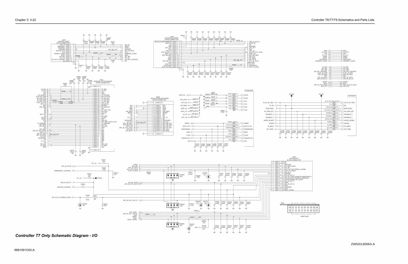
Chapter 3: 3-22 Controller T6/T7/T9 Schematics and Parts Lists
6881091
4
GROUND
FLAT_TX_AUDIO
11
DIG_IN1EXT_MIC_AUDIO
NC
BOOT_CNTRL
1
14
18
RSSI
PCB
16
DIG_IN_3
17
GROUND
DIG_IN_5 WITH WAKEUP (EMERGENCY)
13DIG_IN_OUT_7
2
GM300
SPEAKER-
6
ACCESSORY
7
19
97
9
8
DIG_IN_OUT_4
DIG_OUT2 (EXTERNAL_ALARM)
NC
13
J0501
DIG_IN_6 WITH WAKEUP (IGNITION)FLAT/FILTERED_RX_AUDIO
SWB+
20
12
20-PIN CONNECTOR
20
18
SPEAKER+
WARIS
TO/FROM RF
1
15
DIG_IN_OUT_8
16
3
34
19
NC
1110
2
ROUND
10 12 14
REAR VIEW
BUS+
17
6
OM RF
8
5
5
15
J0501-8
TP0492
J0501-15
SENSE
5V_CNTLR_1
NOISE_BLNKR_CNTLR_1
470pF
J0501-19
C0496
J0501-10
470pFC0497
470pF
MOSBIAS_3_CNTLR_1
C0492
IN_5V_RF_REG_CNTLR_1
J0501-5
IN_5V_RF_REG
DISCAUDIODISCAUDIO_CNTLR_1
J0501-16
INT_SWBINT_SWB_CNTLR_1
470pFC0491
5
J0501-3
16_8MHZ_CNTLR_1
C0495470pF
16_8MHZ
J0501-7
J0501-18
J0501-13
J0501-6
MOSBIAS_2_CNTLR_1
J0501-1
C0493470pF
J0501-12
J0501-2
MOSBIAS_2
J0501-20
VLTG
TP0497
LTG
5V
pF512
J0501-11
NOISE_BLNKR
C0490470pF
J0501-9
0pF518
MOSBIAS_3
C0494470pF
J0501-14
MODIN
PA_PWR_SET_1_CNTLR_1
J0501-4J0501-17
MODIN_CNTLR_1
C0499470pF
PA_PWR_SET
EXP_BD_REQ
GP6_IN_ACC10
GP6_IN_ACC10GP6_IN_ACC10
FLAT_TX_RTN
EXP1_CSGP4_IN_OUT_ACC8OPT_CSRDYOPT_PTT
EXP2_CS
CH_ACT
GP1_IN_ACC3SPI_DATASPI_MISOSPI_CLK
DISCAUDIO
MODIN
OPT_PTTOPT_PTT
INT_MIC INT_MIC
SPKR+SPKR+DISCAUDIO DISCAUDIO
HANDSET_AUDIOHANDSET_AUDIO
RSSI RSSI
IN_5V_RF_REG
GP1_IN_ACC3 GP1_IN_ACC3
INT_SWB+
EXP_BD_REQEXP_BD_REQ
CH_ACT CH_ACT
RDYRDY
5V_RF
NOISE_BLNKR
MOSBIAS_2
PA_PWR_SET
FLAT_TX_RTN FLAT_TX_RTN
GP4_IN_OUT_ACC8 GP4_IN_OUT_ACC8
DISCAUDIO
MOSBIAS_3
VS_MIC VS_MIC
BUS+ BUS+RESETRESET
ON_OFF_CONTROL ON_OFF_CONTROL
16_8MHZ
5VD5VDFLT_A+FLT_A+
EXT_MICEXT_MIC
SPKR-SPKR-
Contr
ZWG0130563-A
C63-A
470pFC0560
NU
R0542
NU
470pFC0576
C0442470pF
NU
C0559470pF
NU
J0451-14
J0551-3
NU
C0558
NU
470pF
J0401-2
NU
390nH
NU
L0482
NU
C05540.1uF
NU INTERNAL OPTION BOARD
3938
9
VS_CS
NC
GROUND
FAST_SQDISCAUDIO
4DB7
DIG_IN_OUT_4
DATA
EXP1_CS
DB2
3
EXP1_CS
5
9V3
5VD
EXT_BD_PTT
EXP_BD_PTT
DATA
36
21
Rx_Aud_SndON
VS_INT
VS_RAC
16
DB3
23
6
RST*
78
INT_EXT_Vdd
GROUND
DB111
7
17
12
NC
J0552
SPI_MISORESET
FLT_A+
26
FLAT_TX_RTN
6
CSX29
12-PIN CONNECTOR
13
CLKMISO
20
SCI_TX
INT_MIC
Tx_Aud_Snd
VS_AUDSEL
SrD_Rtn
5
37
CLK
DISCAUDIOCH_ACT
NCNC
NC
NC
DB6
4
R/W*
Opt_Bd_En
NC
13
10
33
NC
A0
EXT_BD_REQEXT_BD_CSGP4_IN_OUTSPI_CLKSPI_MOSI
DATA
VS_GAINSEL
Gnd
EXP2_CS
NC
EXT_BD_PTT
GND5VD
EXP_BD_PTTGND
RDYOPT_PTT
GND
DB4
CLK
SPEAKER+
14
3
2
8
NC
1011
Key_Row
Key_Intrp
9V3
VS_MIC
5VDHANSET_AUDIO
30
J0451
19
9
VS_CS
11
Flat_Tx_Rtn
NC
12
SrD_Snd
EXT_BD_PTT
27
OPT_CS22
18
40-PIN CONNECTOR
DB5
SCK_Snd
35
NC
NC
78
LED_EN
ON_OFF_CONTROL
1817
NC
1514
16
DIG_IN_6 WITH WAKEUP
Tx_Aud_Rtn
34
Vddd
25
3231
1
7
24
CS*
3NC
NC
3
5
CLK
9
J0551
28
FLT_A+
6
SPEAKER-
OFF_BATT_DATA_OUT
EXP_BD_REQ
EXT_BD_PTT
EXT_BD_PTT
Det_Aud_Snd
12
Rx_Aud_Rtn
1
MISO
2
56
101112
EXP2_CS
8
DB0
DATA
CONTROL HEAD
NC
10
OPT_CS
EXPANSION BOARD
PTT
Rdy/Req
G
4
12
18-PIN CONNECTOR
NC
GND
12
111213
15
40
18-PIN CONNECTORRS232 INTERFACE BOARD
Key_Col
TO/FR
5
6789
10
15161718
4
123
9
14131415161718
J0401
4
GND
BUS+
0R0482
0R0481
470pFC0443
100KR0468
J0552-20
J0552-2
J0552-5J0552-4
R0539
4.7K
J0551-39
J0551-33J0551-34
82pFC0428
DATA_CNTLR_2
J0451-7
J0552-1
C0422
J0551-18
7
470pF
100KR0511
CSX_CNTLR_1J0552-3
VR0510
33V
8
TEMP
9
J0451-12
470pFC0506
0.1uF
J0451-1
C0592
470pFC0478
15KR0512
C0487470pF
R0510
10
4.7K
R0409
5.6VVR0537
C047382pF
8
470pF
J0451-18
C0502
J0401-5
J0551-31
J0451-15
220R0537
J0551-38
RESET
14VVR0541
R0407 10
J0551-5
VR0504
33V
J0551-9
J0551-27
470pFC0474
470pF
J0551-20
C0429
.01uFC0501
470pF
J0451-16
C0426470pFC0445
J0451-8
RSSI_CNTLR_1
R0531
560
DATA
C042182pF
R0525100K
CLK_CNTLR_2
RSSI
C0446470pF
C047282pF
470pFC0484
100K
R0543100K
R0593
R0442 1K
LOCK_CNTLR_1
C0591 0.1uF
TEMPSENSE_CNTLR_1
C0510470pF
J0451-3
J0401-6
9V3
CLK
J0551-32CLK_CNTLR_1
J0551-7
470pFC0476
J0551-13
470pFC0483
J0451-11
J0401-1
C050C0504470pF 470pF470pF
C0503
J0551-24
C05930.1uF
470pFC0430
PASUPVLTG_CNTRL_1
470pF
J0451-10
C0509
0R0412
C0514470pF
VR050520V
J0552-8
J0552-10J0552-9
J0552-11
J0401-10
J0551-40
CSX
R052947K
J0551-41
J0401-4
J0401-7
10R0592
R0401220
J0551-12
J0451-9
J0551-1
VR050320V
J0551-21
RESET_CNTLR_1
1
J0451-6
C0485470pF
R0408
C0477
2
100
J0401-9
470pF
470pFC0447
J0551-22
3J0551-26
TP0530
DATA_CNTLR_1
J0552-17J0552-16
J0401-8
10R0467
C0441
4
J0551-15
J0401-11
J0451-5
470pFC0431
VR050120V
J0551-14
J0551-4
J0551-25
470pFC0515
J0451-13
J0552-12
J0552-14J0552-13
J0552-15
R0538220
R0530
J0401-12
J0451-2
0
C0488
J0551-23
PASUP
470pF
C0513
9V3_CNTLR_1
470pF
8
9
470pF
J0552-18
J0551-28
CNTLV
J0552-19
C047182pF
J0551-10
J0551-19
1KR0535
470pFC0511
470C0
J0551-42
CLK
J0551-16
J0551-2
J0551-30
J0551-35
390nHL0481
470pFC0508
C0448470pF
LOCK
J0552-6
CSX
470pFC0482
J0552-7
VR0509
33V
C0427470pF
J0551-36
47
J0451-17
C0
10
C0575470pF
CSX_CNTLR_2
470pFC0470
27KR0541
J0551-37
47K0.47uFC0541
J0551-8
0R0441
9
J0551-6
.01uFC0516 C0517
82pF
C0486470pF
DATA
J0551-29
C0542
C0423470pF
47uF
R0533 0
J0451-4
24KR0591
CNTLVLTG_CNTLR_1J0551-17
470pFC0449
J0551-11
J0401-3
5VD
SPKR-SPKR+
ON_OFF_CONTROL
SPKR-
FLAT_TX_RTN
GP6_IN_ACC10
SPI_DATA
EXT_MICGP1_IN_ACC3
GP2_OUT_ACC4
GP5_IN_ACC9
GP7_IN_OUT_ACC12
GP8_IN_OUT_ACC14
SPKR+
GP3_IN_ACC6GP4_IN_OUT_ACC8
EXP2_CS
9V3
SPI_MISO
CH_ACT
5VD9V3
5VDSPI_MISO
RESET
FLT_A+
DISCAUDIO
GP4_IN_OUT_ACC8EXP1_CS
EXP_BD_REQGP1_IN_ACC3
SPI_CLK
OPT_PTT
INT_MIC
HANDSET_AUDIO
BOOT_CNTRL
5VD
BUS+
GP1_IN_ACC3
5VD
GP4_IN_OUT_ACC8EXP1_CS
EXP_BD_REQGP1_IN_ACC3
CH_ACTDISCAUDIO
FLT_A+
SCI_TX
RX_FLAT_FILTERED_AUDIO
EMERGENCY_CONTROL
FLT_A+
RSSI
EXT_SWB+
RDY
EXP1_CS
9V3
SPI(0:10)
FLAT_TX_RTN
FLT_A+
SPI_DATA
SPI_CLK
SPI_MISO
VS_CS
OPT_CSRESET
RESET
PASUPVLTG
BUS+
TEMPSENSE
CNTLVLTG
RSSI
LOCK
OPT_CS
SPI_DATA
TX_AUD_RTN
VS_CSVS_MIC
SPI_CLK
FLAT_RX_SNDRX_AUD_RTN
URX_SND
TX_AUD_SND
VS_INT
5VDVS_AUDSEL
VS_GAINSELSPI_MISO
VS_RAC
IGNITION_CONTROL
FLT_A+
F04013A
oller T7 Only Schematic Diagram - I/O
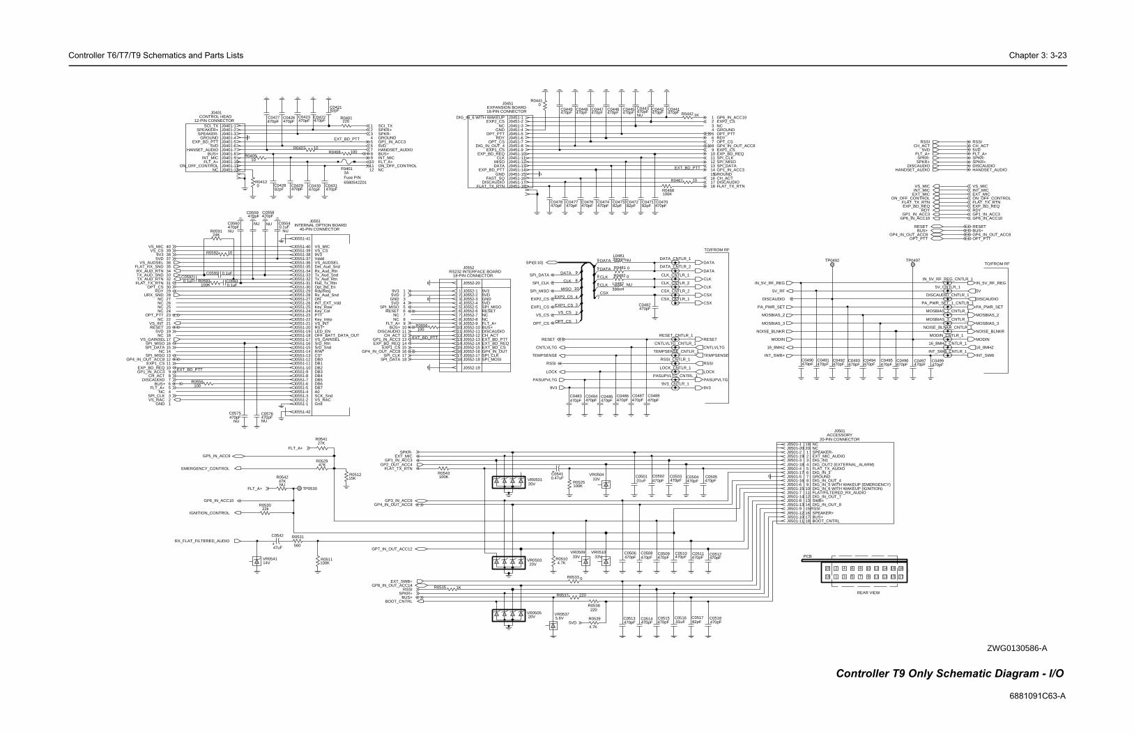
Controller T6/T7/T9 Schematics and Parts Lists Chapter 3: 3-23
6881091C63-A
4
GROUND
FLAT_TX_AUDIO
11
DIG_IN1
3
EXT_MIC_AUDIO
NC
BOOT_CNTRL
16
1
14
18
RSSI
6
PCB
16
DIG_IN_3
17
GROUND
5
DIG_IN_5 WITH WAKEUP (EMERGENCY)
13DIG_IN_OUT_7
2
GM300
SPEAKER-
6
ACCESSORY
7
4
19
9
13
10
7
9
8
14
8
DIG_IN_OUT_4
DIG_OUT2 (EXTERNAL_ALARM)
NC
13
J0501
DIG_IN_6 WITH WAKEUP (IGNITION)FLAT/FILTERED_RX_AUDIO
9
SWB+
20
11
_PTT
12
20-PIN CONNECTOR
1817
20
18
SPEAKER+
WARIS
TO/FROM RF
7
1
15
DIG_IN_OUT_8
16
3
34
19
12
NC
12
1110
2
GROUND
10 12 14
REAR VIEW
BUS+
17
15
6
TO/FROM RF
8
5
5
15
J0501-8
TP0492
J0501-15
TEMPSENSE
5V_CNTLR_1
NOISE_BLNKR_CNTLR_1
RESET
470pF
J0501-19
C0496
J0501-10
470pFC0497
DATA
470pF
MOSBIAS_3_CNTLR_1
C0492RSSI
IN_5V_RF_REG_CNTLR_1
J0501-5
IN_5V_RF_REG
DISCAUDIO
2 1K
DISCAUDIO_CNTLR_1
R_1
J0501-16
9V3
CLK
INT_SWBINT_SWB_CNTLR_1
470pFC0491
C05055040pF 470pF
L_1
J0501-3
CSX
16_8MHZ_CNTLR_1
C0495470pF
16_8MHZ
J0501-7
1
J0501-18
J0501-13
J0501-6
MOSBIAS_2_CNTLR_1
10
J0501-1
C0493470pF
J0501-12
J0501-2
MOSBIAS_2
J0501-20
PASUPVLTG
TP0497
CNTLVLTG
5V
470pFC0511
470pFC0512
CLK
J0501-11
NOISE_BLNKR
LOCK
CSX
C0490470pF
J0501-9
470pFC0518
MOSBIAS_3
C0494470pF
J0501-14
MODIN
PA_PWR_SET_1_CNTLR_1
J0501-4J0501-17
MODIN_CNTLR_1
C051782pF
DATA
C0499470pF
PA_PWR_SET
_1
EXP_BD_REQ
GP6_IN_ACC10
GP6_IN_ACC10GP6_IN_ACC10
FLAT_TX_RTN
EXP1_CSGP4_IN_OUT_ACC8OPT_CSRDYOPT_PTT
EXP2_CS
CH_ACT
GP1_IN_ACC3SPI_DATASPI_MISOSPI_CLK
DISCAUDIO
MODIN
OPT_PTTOPT_PTT
INT_MIC INT_MIC
SPKR+SPKR+DISCAUDIO DISCAUDIO
HANDSET_AUDIOHANDSET_AUDIO
RSSI RSSI
IN_5V_RF_REG
GP1_IN_ACC3 GP1_IN_ACC3
INT_SWB+
EXP_BD_REQEXP_BD_REQ
CH_ACT CH_ACT
RDYRDY
5V_RF
NOISE_BLNKR
MOSBIAS_2
PA_PWR_SET
FLAT_TX_RTN FLAT_TX_RTN
GP4_IN_OUT_ACC8 GP4_IN_OUT_ACC8
DISCAUDIO
MOSBIAS_3
VS_MIC VS_MIC
BUS+ BUS+RESETRESET
ON_OFF_CONTROL ON_OFF_CONTROL
16_8MHZ
5VD5VDFLT_A+FLT_A+
EXT_MICEXT_MIC
SPKR-SPKR-
ZWG0130586-A
ZWG0130586-A
Controller T9 Only Schematic Diagram - I/O
470pFC0560
NU
R0542
NU
470pFC0576
C0442470pF
NU
C0559470pF
NU
J0451-14
J0551-3
NU
C0558
NU
470pF
J0401-2
NU
390nH
NU
L0482
NU
C05540.1uF
NU INTERNAL OPTION BOARD
3938
9
VS_CS
NC
GROUND
FAST_SQDISCAUDIO
4DB7
DIG_IN_OUT_4
DATA
EXP1_CS
DB2
EXP1_CS
5
9V3
5VD
EXT_BD_PTT
EXP_BD_PTT
DATA
36
21
Rx_Aud_SndON
VS_INT
VS_RAC
DB3
23
6
RST*
78
INT_EXT_Vdd
GROUND
DB111
7
17
12
BUS+
J0552
SPI_MISORESET
FLT_A+
26
FLAT_TX_RTN
CSX29
12-PIN CONNECTOR
13
CLKMISO
20
SCI_TX
INT_MIC
Tx_Aud_Snd
VS_AUDSEL
SrD_Rtn
37
CLK
DISCAUDIOCH_ACT
NCNC
BUS+
NC
DB6
R/W*
Opt_Bd_En
NC
33
NC
A0
EXT_BD_REQEXT_BD_CSGP4_IN_OUTSPI_CLKSPI_MOSI
DATA
VS_GAINSEL
Gnd
EXP2_CS
BUS+
EXT_BD_PTT
GND5VD
EXP_BD_PTTGND
RDYOPT_PTT
GND
DB4
CLK
SPEAKER+3
2
NC
1011
Key_Row
Key_Intrp
9V3
VS_MIC
5VDHANSET_AUDIO
30
J0451
19
VS_CS
Flat_Tx_Rtn
NC
12
SrD_Snd
EXT_BD
27
OPT_CS22
18
40-PIN CONNECTOR
DB5
SCK_Snd
35
NC
NC
78
LED_EN
ON_OFF_CONTROL
NC
1514
16
DIG_IN_6 WITH WAKEUP
Tx_Aud_Rtn
34
Vddd
25
3231
1
24
CS*
3NC
NC
3
5
CLK
9
J0551
28
FLT_A+
6
SPEAKER-
OFF_BATT_DATA_OUT
EXP_BD_REQ
EXT_BD_PTT
EXT_BD_PTT
Det_Aud_SndRx_Aud_Rtn
MISO
56
101112
EXP2_CS
8
DB0
DATA
CONTROL HEAD
NC
10
OPT_CS
EXPANSION BOARD
PTT
Rdy/Req
4
12
18-PIN CONNECTOR
NC
GND
12
111213
40
18-PIN CONNECTORRS232 INTERFACE BOARD
Key_Col
5
6789
10
15161718
4
123
9
14131415161718
J0401
4
GND
BUS+
0R0482
0R0481
470pFC0443
100KR0468
J0552-20
J0552-2
J0552-5J0552-4
R0539
4.7K
J0551-39
J0551-33J0551-34
82pFC0428
DATA_CNTLR_2
J0451-7
J0552-1
C0422
J0551-18
7
470pF
100KR0511
CSX_CNTLR_1J0552-3
VR051033V
8
9
J0451-12
470pFC0506
0.1uF
J0451-1
C0592
470pFC0478
15KR0512
C0487470pF
R0510
10
4.7K
R0409
5.6VVR0537
C047382pF
8
470pF
J0451-18
C0502
J0401-5
J0551-31
J0451-15
220R0537
J0551-38
14VVR0541
R0407 10
J0551-5
VR050433V
J0551-9
J0551-27
470pFC0474
470pF
J0551-20
C0429
.01uFC0501
470pF
J0451-16
C0426470pFC0445
J0451-8
RSSI_CNTLR_1
R0531
560
C042182pF
R0525100K
CLK_CNTLR_2
C0446470pF
C047282pF
470pFC0484
100K
R0543100K
R0593
R044
LOCK_CNTLR_1
C0591 0.1uF
TEMPSENSE_CNTL
C0510470pF
J0451-3
J0401-6
J0551-32CLK_CNTLR_1
J0551-7
470pFC0476
J0551-13
470pFC0483
J0451-11
J0401-1
C047470pF
C0503
J0551-24
C05930.1uF
470pFC0430
PASUPVLTG_CNTR
470pF
J0451-10
C0509
0R0412
C0514470pF
VR050520V
J0552-8
J0552-10J0552-9
J0552-11
J0401-10
J0551-40
R052947K
J0551-41
J0401-4
J0401-7
10R0592
R0401220
J0551-12
J0451-9
J0551-1
VR050320V
J0551-21
RESET_CNTLR_
1
J0451-6
C0485470pF
R0408
C0477
2
100
J0401-9
470pF
470pFC0447
J0551-22
3J0551-26
TP0530
DATA_CNTLR_1
J0552-17J0552-16
J0401-8
R0467
C0441
4
J0551-15
J0401-11
J0451-5
470pFC0431
VR050120V
J0551-14
J0551-4
J0551-25
470pFC0515
J0451-13
J0552-12
J0552-14J0552-13
J0552-15
R0538220
R0530
J0401-12
J0451-2
22k
C0488
J0551-23
470pF
C0513
9V3_CNTLR_1
470pF
8
9
470pF
J0552-18
J0551-28
J0552-19
C047182pF
J0551-10
J0551-19
1KR0535
J0551-42
J0551-16
J0551-2
J0551-30
J0551-35
390nHL0481
470pFC0508
C0448470pF
J0552-6470pFC0482
J0552-7
VR050933V
C0427470pF
J0551-36
J0451-17
10
C0575470pF
CSX_CNTLR_2
470pFC0470
27KR0541
J0551-37
47K0.47uFC0541
J0551-8
0R0441
9
J0551-6
.01uFC0516
C0486470pF
J0551-29
C0542
C0423470pF
47uF
R0533 0
J0451-4
24KR0591
CNTLVLTG_CNTLRJ0551-17
470pFC0449
J0551-11
J0401-3
5VD
SPKR-SPKR+
ON_OFF_CONTROL
SPKR-
FLAT_TX_RTN
GP6_IN_ACC10
SPI_DATA
EXT_MICGP1_IN_ACC3
GP2_OUT_ACC4
GP5_IN_ACC9
GP7_IN_OUT_ACC12
GP8_IN_OUT_ACC14
SPKR+
GP3_IN_ACC6GP4_IN_OUT_ACC8
EXP2_CS
9V3
SPI_MISO
CH_ACT
5VD9V3
5VDSPI_MISO
RESET
FLT_A+
DISCAUDIO
GP4_IN_OUT_ACC8EXP1_CS
EXP_BD_REQGP1_IN_ACC3
SPI_CLK
OPT_PTT
INT_MIC
HANDSET_AUDIO
BOOT_CNTRL
5VD
BUS+
GP1_IN_ACC3
5VD
GP4_IN_OUT_ACC8EXP1_CS
EXP_BD_REQGP1_IN_ACC3
CH_ACTDISCAUDIO
FLT_A+
SCI_TX
RX_FLAT_FILTERED_AUDIO
EMERGENCY_CONTROL
FLT_A+
RSSI
EXT_SWB+
RDY
EXP1_CS
9V3
SPI(0:10)
FLAT_TX_RTN
FLT_A+
SPI_DATA
SPI_CLK
SPI_MISO
VS_CS
OPT_CSRESET
RESET
PASUPVLTG
BUS+
TEMPSENSE
CNTLVLTG
RSSI
LOCK
OPT_CS
SPI_DATA
TX_AUD_RTN
VS_CSVS_MIC
SPI_CLK
FLAT_RX_SNDRX_AUD_RTN
URX_SND
TX_AUD_SND
VS_INT
5VDVS_AUDSEL
VS_GAINSELSPI_MISO
VS_RAC
IGNITION_CONTROL
FLT_A+
F04013AFuse P/N6580542Z01
100R0556
100R0556

Chapter 3: 3-24 Controller T6/T7/T9 Schematics and Parts Lists
6881091
HC138_A2
GP1_IN
GP7_IN
GP5_IN
- R0105 USED INSTANDARD ONLY- R0106 USED INPRIME ONLY
HC138_A0
GP6_IN
GP8_IN
GP3_INPE6
GP4_IN
GP2_OUT
GP8_OUT
HC138_A1
GP4_OUT
GP7_OUT
47K
47K
47K
47K
47K
47K
47K
R0179
R0172
10K
R017510K
C01071000pF
R0170
11
10K
10
1
7
12
R01854.7K
2.2KR0108
3
9
Q0181
6
47K
R0184
10K
47K
47K
R0174
Q0185
R01834.7K
Q0173
R01734.7K
4
4.7KR0177
8
D0179
4.7KR0181
100KR0105
R0178
47K
47K
47K
4.7KR0171
Q0171
Q0177
R0186
30K
47K
R0176
13
5
47K
R0182
0NU
R0106
Q0183
5VD
GP1_IN_ACC3
GP6_IN_ACC10
GP2_OUT_ACC4
GP4_IN_OUT_ACC8
GP3_IN_ACC6
5VD
RESET
RESET
5VD
GP5_IN_ACC9
GPIO(0:13)
GPIO(0:13)
5VD
5VD
FLT_A+
5VD
GP7_IN_OUT_ACC12
GP8_IN_OUT_ACC14
5VD
5VD
5VD
5VD
FL0830683O
FL0830683-OContro
C63-A
HS
IO
GP4_OUTGP7_OUT
GP8_OUT
EXP1_CS
EE
_CS
HS
IO
CLK
GP1_IN
CLK
CS
XGP7_OUT
VO
X
LSIO
GP7_IN
REF_CS
MIS
O
EXP2_CS
512kx8bit
RAM
GP6_IN
HC138_A0
GP3_IN
GP8_IN
LVZIF_CS
SQ
_DE
T
HC138_A1
FLASH ROM
SY
N
HC138_A2
LSIO
MICROPROCESSORD
AT
AMIS
O
F12
00
GP4_IN
GP5_IN
GP4_OUT
VS_CS
ON_OFF_SENSE
EEPROM
DA
TA
32kx8bit
OPT_CS
CH
AC
T
16Kx8bit
(EXT_BD_PTT & DATA_PTT)
EE_CS
0R0116
NU
4
R015224K
R0132330K
2
6
7
R0115
0R0111
10K
7
10
1
100pFC0101
9 0
11
6
R011410K
10K
R0104
69V
RL
68
VS
S13
VS
SL
40V
SS
R87
93X
FC
XIRQ 48
XT
AL
91
76
PJ6 77
PJ7 78
RESET 94
VD
D12
VD
DL
39V
DD
R88
VD
DS
YN
92
VR
H
51P
I650
PI7
49
PJ0_CSGP3 71
PJ1_CSGP4 72
PJ2 73
PJ3 74
PJ4 75
PJ5
42
PH6_CSGP241
PH7_CSPROG38
PI0
56P
I155
PI2
54P
I353
PI4
52P
I5
18
PG6_AS5
PG7_R_W 4
PH0_PW147
PH1_PW246
PH2_PW345
PH3_PW444
PH4_CSIO43
PH5_CSGP1
23P
F7_
AD
DR
722
PF
O_A
DD
R0
29
PG0_XA136
PG1_XA1416
PG2_XA1520
PG3_XA1619
PG4_XA1717
PG5_XA18
PE5_AN561PE6_AN660PE7_AN7
PF
1_A
DD
R1
28P
F2_
AD
DR
227
PF
3_A
DD
R3
26P
F4_
AD
DR
425
PF
5_A
DD
R5
24P
F6_
AD
DR
6
1P
D5_
SS
23P
D6_
LVIN
67PE0_AN066PE1_AN165PE2_AN264PE3_AN363PE4_AN462
34
PC5_DATA535
PC6_DATA636
PC7_DATA737
PD
0_R
XD
97P
D1_
TX
D98
PD
2_M
ISO
99P
D3_
MO
SI
100
PD
4_S
CK
15P
B6_
AD
DR
148
PB
7_A
DD
R15
7
PB
O_A
DD
R8
14
PC0_DATA030
PC1_DATA131
PC2_DATA232
PC3_DATA333
PC4_DATA4
83P
A5_
OC
3_O
C1
84P
A6_
OC
2_O
C1
85P
A7_
PA
1_O
C1
86
PB
1_A
DD
R9
10P
B2_
AD
DR
1011
PB
3_A
DD
R11
9P
B4_
AD
DR
1221
PB
5_A
DD
R13
96
95LV
OU
T
MODA_LIR 58
MODB_VSTBY 57
PA
0_IC
379
PA
1_IC
280
PA
2_IC
181
PA
3_IC
4_O
C5_
OC
182
PA
4_O
C4_
OC
1
U0101
AV
DD
59
AV
SS
70
ECLK 89
EX
TA
L90
IRQ
5
0
4
3WP
1CS
7HOLD
6SCK
5SI
2SO
8V
CC
4
VS
S
X25128-2.7U0111
.01uFC0151
47K
47K
0.1uFC014
7
1
C0106100pFNU
3
0
15 Y014 Y113 Y212 Y311 Y410 Y59 Y67 Y7
1A02A13A2
6EN_CS1
4EN_CS25EN_CS3
8G
ND
16
VCC
12
MC74HC138A
U0141
TP0102
65
6
10
IO617
IO718
IO819
VC
C
28
8
2
6
EN_OE22
EN_WE27
14G
ND
IO111
IO212
IO313
IO415
IO516A3 7
A4 65A5
A6 4
A7 3
A8 25
A9 24
EN_CS20
A0 10
A1 9
21A10A11 23
A12 2
A13 26
A14 1
A2 8
6
U0122
63A21
8
17
10
6
0.1uF
7
TP0151
C0121
C0102100pF
NU NU
18
C0104100pF
22pFC0132
0
12
3
1
11
4 13
12
013
D0151
122
3
1
8
8
18
R0110
NU
7
10K
9
1
4
5
1
1
C0122
7
109
0.1uF
3
2
TP0103
3
11 1
10
7
2
1
2
C0123
NU
0.1uF
100pF
C0112
10KR0113
R015124K
2
8
0
22IO123IO225IO326IO427IO528IO629IO7
VCC8
13 A73 A82 A9
30 EN_CE32 EN_OE7 EN_WE
GN
D24
IO0 21
10 A166 A179 A18
18 A217 A316 A4
A515
A614
20 A019
A1
31 A101 A11
12 A12A134
5 A14A1511
3
AT49F040
U0121
23
17
9
5
6
7
10KR0101
TP0101
Q0110
47K
47KR0107
NU
3
47K
4
3
5
10MEG
R0131
NU
4
2
100pFC0105
4
D0101
3.9KR0117
15
5
1413
16
5
100K
5
R0121
3
Q0151
0
10
0
6
13
4
IN1
9
0
6
1
38.40KHz
Y0131XTAL
NC
2
NC1
3
OUT4
NU
R0112
0
8
16
100pF
C0111
NU
C0103
NU
R01024.7K
100pF
22pFC0131
15
7
VR0151
14
9
4
5
0
2
R_W
RAM_CS
BUS+
CNTLVLTG
SCI_TX
R_W
FLASH_CEFLASH_OE
5VD
IRQ
IRQ
ADDR_BUS(0:18)
DATA_BUS(0:7)
14
FROM_U0101_47
VS_RAC
5VD
VS_INT
5VDBOOT_CNTRL
5VD
TP0104
ON_OFF_CONTROL
5VD
5VD
5VD
OPT_PTT
5VD
SPI(0:10)SPI(0:10) SPI(0:10) SPI(0:10)
CNTLR_AUDIO(0:7)CNTLR_AUDIO(0:7)CNTLR_AUDIO(0:7)
FROM_U0101_47FROM_U0101_46
FROM_U0101_46
TEMPSENSE
RAM_CS
5VD
VS_GAINSEL
EXT_BD_REQ
RSSI
RX_ADAPT
5VD
5VD5VD
FLT_A+ FLT_A+
FLASH_OE
NC
ECLK
NC
NC
LOCK
RDY
ON_OFF_CONTROL
FLASH_CE
R_W
VSTBY
5VD
BATTERY_VOLTAGE
ller T6/T7 Schematic Diagram - Microprocessor

Controller T6/T7/T9 Schematics and Parts Lists Chapter 3: 3-25
6881091C63-A
0
4.7KR0171
NU
R0182
R0106 0Used inprimeonly
GP3_IN
GP8_IN
PE6
GP7_IN
HC138_A0
HC138_A2
GP1_IN
GP8_OUT
HC138_A1HC138_A2
GP2_OUT
GP4_IN
GP1_IN
GP5_INGP7_IN
GP5_IN
S
GP4_OUT
GP7_OUT
ATA_PTT)
HC138_A0
GP3_IN
GP8_IN
GP6_IN
GP6_IN
GP4_OUTGP7_OUT
GP4_IN
GP8_OUT
HC138_A1
10K
R0172
10KR0175
10
1
1000pFC0107
R011410K
R010410K
10KR0170
4
10
11
47K
R0179
0.1uFC0141
79 Y67 Y7
12
8GND
16VCC15 Y0
14 Y113 Y212 Y311 Y410 Y5
8A
U0141 1A02A13A2
6EN_CS1 4EN_CS2 5EN_CS3
6
R01854.7K
6
9
Q0181
47KR0184
10KR0174
Q0185
1
13
Q0173
C0106100pF
R0173
12
4.7K
4
3
2.2KR0108
8
4.7K
3
R0183
0
8
D0179
7
4.7KR0177
100KUsed instandard only
R0105
2
2
5
13
9
47K
4.7KR0181
R0178 47K
Q0183
5
Q0171
Q0177
47KR0186
R0176
30K
CNTLVLTG
5VD
GP1_IN_ACC3
GP6_IN_ACC10
GP2_OUT_ACC4
5VD
IRQ
M_U0101_47
VS_RAC
5VD
VS_INT
GP4_IN_OUT_ACC8
5VD
GP3_IN_ACC6
5VD
RESET
RESET
5VD
GP5_IN_ACC9
GPIO(0:13)
GPIO(0:13)
M_U0101_46
5VD
5VD
FLT_A+
TEMPSENSE
VS_GAINSEL
EXT_BD_REQ
RSSI
5VD
LOCK
GP7_IN_OUT_ACC12
GP8_IN_OUT_ACC14
5VD
5VD
5VD
5VD
VSTBY
BATTERY_VOLTAGE
ZWG0130585-A
Controller T9 Only Schematic Diagram - Microprocessor
4
0
18
100pFC0104
NU
C0102100pFNU
12
NU
R011010K
NU
18
NU
0.1uF
100pF
NU
NU
R01024.7K
NU
NU
8
16
NU
VO
X
LSIO
REF_CS
SQ
_DE
T
FLASH ROM
SY
N
LSIO
MICROPROCESSOR
DA
TA
MIS
O
F12
00
EEPROM
DA
TA
EE
_CS
VS_CSEXP1_CS
CLK
CS
X
GP4_OUTGP7_OUT
CLK
32kx8bit
OPT_CS
LVZIF_C
16Kx8bit
(EXT_BD_PTT & D
EE_CS
512kx8bit
RAM
MIS
O
EXP2_CS
HS
IO
ON_OFF_SENSE
CH
AC
T
HS
IO
6
2
7
R0111
10KR0115
0C0101
7
9
100pF
0
5
0
R0116
7
R015224K
R0132330K
3
MC74HC13
5
12
TP0102
6
6
10
2IO415IO516IO617IO718IO819
VCC
28
8
A9 24
EN_CS 20
EN_OE 22
EN_WE 27
14GND
IO111IO212IO313
A14 1
A2 8A3 7A4 6
5A5A6 4A7 3A8 25
A0 10A1 9
21A10A11 23A12 2A13 26
11
6
U012263A21
8
6
VS
SL
40V
SS
R87
93X
FC
XIRQ 48
XT
AL
91
RESET 94
VD
D12
VD
DL
39V
DD
R88
VD
DS
YN
92
VR
H69
VR
L68
VS
S13
PJ0_CSGP3 71
PJ1_CSGP4 72
PJ2 73
PJ3 74
PJ4 75
PJ5 76
PJ6 77
PJ7 78
56P
I155
PI2
54P
I353
PI4
52P
I551
PI6
50P
I749
PH0_PW147PH1_PW246PH2_PW345PH3_PW444PH4_CSIO43PH5_CSGP142PH6_CSGP241PH7_CSPROG38
PI0
PG0_XA136
PG1_XA1416
PG2_XA1520
PG3_XA1619
PG4_XA1717PG5_XA1818
PG6_AS5
PG7_R_W 4
PF
1_A
DD
R1
28P
F2_
AD
DR
227
PF
3_A
DD
R3
26P
F4_
AD
DR
425
PF
5_A
DD
R5
24P
F6_
AD
DR
623
PF
7_A
DD
R7
22
PF
O_A
DD
R0
29
67PE0_AN0 66PE1_AN1 65PE2_AN2 64PE3_AN3 63PE4_AN4 62PE5_AN5 61PE6_AN6 60PE7_AN7PC7_DATA737
PD
0_R
XD
97P
D1_
TX
D98
PD
2_M
ISO
99P
D3_
MO
SI
100
PD
4_S
CK
1P
D5_
SS
23P
D6_
LVIN
PB
O_A
DD
R8
14
PC0_DATA030PC1_DATA131PC2_DATA232PC3_DATA333PC4_DATA434PC5_DATA535PC6_DATA636
PA
7_P
A1_
OC
186
PB
1_A
DD
R9
10P
B2_
AD
DR
1011
PB
3_A
DD
R11
9P
B4_
AD
DR
1221
PB
5_A
DD
R13
15P
B6_
AD
DR
148
PB
7_A
DD
R15
7
MODB_VSTBY 57
PA
0_IC
379
PA
1_IC
280
PA
2_IC
181
PA
3_IC
4_O
C5_
OC
182
PA
4_O
C4_
OC
183
PA
5_O
C3_
OC
184
PA
6_O
C2_
OC
185
AV
DD
59
AV
SS
70
ECLK 89EX
TA
L90
IRQ 96
95LV
OU
T
MODA_LIR 58
MC68HC11FL0
U0101
22pFC0132
0
7HOLD
6SCK
5SI
2 SO
8VCC
4VSS
3WP
X25128-2.7U0111
1CS
.01uFC0151
D0151
2
3
1
8
8
6
1
1
17
10
1
4
5
7
TP0151
C01210.1uF
0.1uFC0122
TP0103
1
103
2
2
3
11
1
11
121
10KR0113
R015124K
3
0
13
4
2
6
17
9
10KR0101
5
7
TP0101
3
Q0110
47KR0107
9 9
4
7
10
100pFC0105
4
D0101
3.9K
R01175
1413
16
5
C0123
7
5
C0112
Q0151
28IO629IO7
VCC
8
2
0
3
7 EN_WE
GND24
IO0 2122IO1 23IO225IO326IO427IO5
16 A4A515A614
13 A73 A82 A9
30 EN_CE32 EN_OE
A1345 A14
A151110 A16
6 A179 A18
18 A217 A3
AT49F040
U0121
20 A019 A1
31 A101 A1112 A12
43
1
6
13
2
NC1
3
OUT4
IN 1
0
6
38.40KHz
Y0131XTAL
NC
R0112
0
4
3
5
10MEG
R0131
100pFC0111
100pFC0103
22pFC0131
15
9
7
VR01515.6V
14
TP0104
1514
4
0
2100K
R0121
10
R_W
RAM_CS
BUS+
SCI_TX
R_W
FLASH_CEFLASH_OE
IRQ
ADDR_BUS(0:18)
DATA_BUS(0:7)
0
FRO
BOOT_CNTRL
5VD
ON_OFF_CONTROL
5VD
5VD
5VD
OPT_PTT
5VD
SPI(0:10)SPI(0:10) SPI(0:10) SPI(0:10) SPI(0:10)
CNTLR_AUDIO(0:7) CNTLR_AUDIO(0:7)CNTLR_AUDIO(0:7)CNTLR_AUDIO(0:7)
FROM_U0101_47FROM_U0101_46
FRO
RAM_CS
5VD
RX_ADAPT
5VD
5VD5VD
FLT_A+ FLT_A+
FLASH_OE
NC
_XT
AL
ECLK
RDY
ON_OFF_CONTROL
FLASH_CE
R_W
5VD
NU10
R0103C01080,1uF
5VDC (0VDC during On/Off pressed and during head request)
5VDC (0VDC during boot mode)
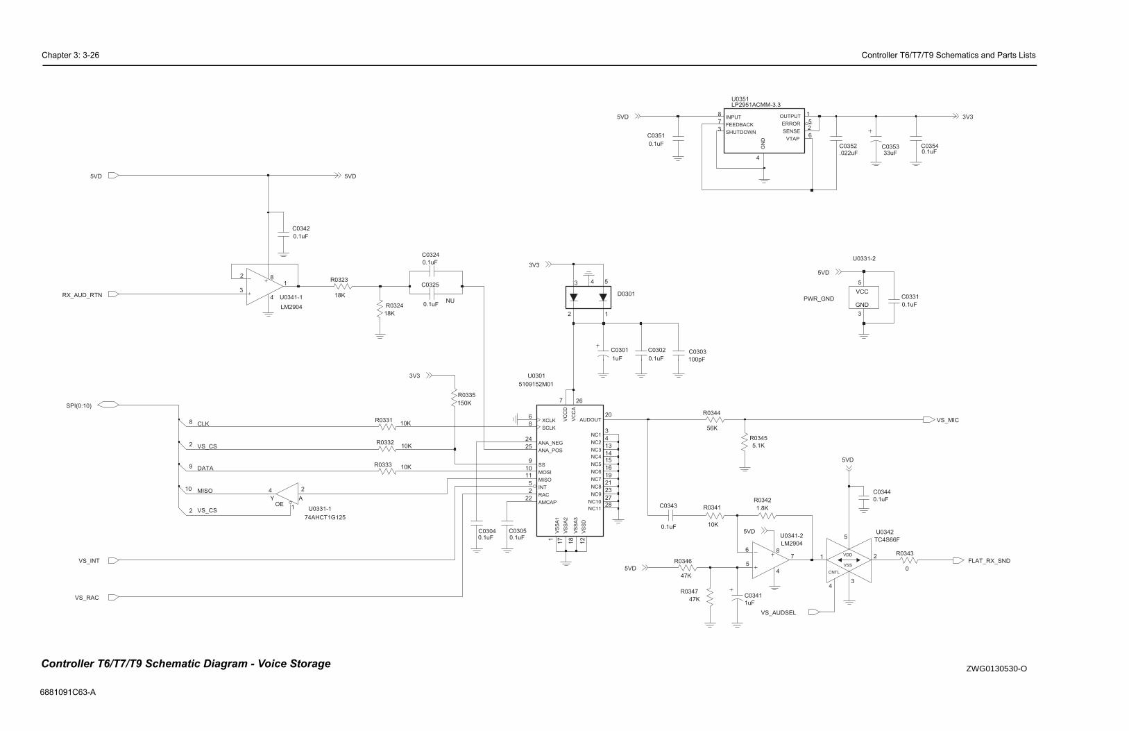
Chapter 3: 3-26 Controller T6/T7/T9 Schematics and Parts Lists
6881091
C0331
0.1uF
U0331-2
PWR_GND
3
GND
5
VCC
C03540.1uF
U0341-2
LM29046
5
78
4
2
5
VDD
3
VSS
6
R0343
0
RX
5VD
FLAT_RX_SND
S
C0303
100pF
U0351LP2951ACMM-3.3
33uFC0353
.022uFC0352
10K
R0341
U0342
TC4S66F
4
CNTL
1
K
6
47K
347
1uF
C0341
C0344
0.1uF
56K
R0344
5.1K
R0345
1.8K
R0342
ERROR 5FEEDBACK
7
GN
D
4
INPUT8 OUTPUT 1
SENSE2
SHUTDOWN3
VTAP
VS_MIC
3V3
5VD
5VD
VS_AUDSEL
Contr ZWG0130530-O
C63-A
9
C0325
0.1uFNU
10KR0332
2
C0342
18K
0.1uF
C0302
10
_AUD_RTN
3V3
PI(0:10)
R0324
0.1uFC0305
0.1uF
C0343
0.1uF
1uF
C0324
2
C0351
0.1uF
74AHCT1G125
U0331-1
2
A
1OE
4
Y
10KR0333 SS9
VC
CA
26
VC
CD
7
VS
SA
1
1
VS
SA
21
7
VS
SA
31
8
VS
SD
12
XCLK6
D0301
53
12
48
4
47
R034
R0
0.1uFC0304
LM2904
U0341-1
2
31
8
0.1uF
C0301
CLK
DATA
5109152M01
VS_CS
MISO
VS_CS
R0335
150K
NC414
NC515
NC616
NC719
NC821
NC923
RAC2
SCLK8
INT
MISO11
MOSI10
NC13
NC1027
NC1128
NC24
NC313
U0301
22AMCAP
ANA_NEG24
ANA_POS25
AUDOUT20
5
10KR0331
18K
R0323
VS_RAC
3V3
5VD
5VD5VD
VS_INT
5VD
oller T6/T7/T9 Schematic Diagram - Voice Storage

C Chapter 3: 3-27
6881091C63-A
C
70 pF 10%70 pF 10%70 pF 10%70 pF 10%70pF 50V70 pF 10%70 pF 10%70 pF 10%70 pF 10%70 pF 10%70 pF 10%70 pF 10%70 pF 10%70 pF 10%70 pF 10%70 pF 10%70 pF 10%70 pF 10%0nF 50V70pF 10% (CNTRL T6)70pF 50V (CNTRL T7)70pF 10% (CNTRL T6)70pF 50V (CNTRL T7)70pF 50V70pF 10% (CNTRL T6)70pF 50V (CNTRL T7)70pF 10% (CNTRL T6)70pF 50V (CNTRL T7)70pF 10% (CNTRL T6)70pF 50V (CNTRL T7)70pF 10% (CNTRL T6)70pF 50V (CNTRL T7)70pF 50V70pF 10% (CNTRL T6)70pF 50V (CNTRL T7)70pF 10% (CNTRL T6)70pF 50V (CNTRL T7)70pF 50V70pF 10% (CNTRL T6)70pF 50V (CNTRL T7)70pF 10% (CNTRL T6)70pF 50V (CNTRL T7)0nF 50V2.0 pF 5%70pF 10% (CNTRL T6)70pF 50V (CNTRL T7)70nF 10% 25V7uF 20% 10V00nF 16V00nF 16V.1uF, 0662057B47, 0 Kohm esistor for LS+ models
Description
C0601 2113741F17 470pF 50VC0603 2380090M24 LYT 10uF 50V 20%C0611 2311049C06 CP 22uF 20% 35VC0612 2113743E20 100nF 16VC0622 2311049A99 CP 47uF 20%C0641 2113741F17 470pF 50VC0644 2311049A97 CHIP 33 uFC0645 2113743E20 100nF 16VDC0652 2311049A97 CHIP 33 uF 16C0654 2311049A57 CP 10uF 10% 16VC0655 2113743E20 100nF 16VC0661 2311049C05 CP 47uF 10% 16VC0662 2113741F49 10nF 50VC0663 2113743E20 100nF 16VC0671 2113743E20 100nF 16VC0681 2113743E20 100nF 16VD0101 4880236E05 CHIP SCHOTTKYD0151 4813833C02 DUAL SOT MMBD6100D0179 4813833C02 DUAL SOT MMBD6100D0301 4802245J47 SCHOTTKY BARRIER
(RB471E) Voice storage only
D0621 4813833C02 DUAL SOT MMBD6100D0651 4813833C02 DUAL SOT MMBD6100D0660 4813833C02 DUAL SOT MMBD6100D0661 4813833C02 DUAL SOT MMBD6100E0271 2484657R01 Ferrite BeadE0272 2484657R01 Ferrite BeadE0631 2484657R01 Ferrite BeadF0401 6580542Z01 3A 24VJ0401 0902636Y02 CONN FLEX 12 PINJ0451 0902636Y01 CONN FLEX SIDE ENTRYJ0501 0986105B01 CONN SMD 20 PINJ0551 0905505Y04 CONN ZIF HORIZONTALJ0552 0905505Y03 CONN ZIF 18PINJ0601 0986165B01 DC PWR CONNQ0110 4880048M01 NPN DIG 47k/47kQ0151 4880048M01 NPN DIG 47k/47kQ0171 4880048M01 NPN DIG 47k/47kQ0173 4880052M01 NPN DRLNGTN MXTAQ0177 4880048M01 NPN DIG 47k/47kQ0181 4880048M01 NPN DIG 47k/47kQ0183 4880048M01 NPN DIG 47k/47kQ0185 4880048M01 NPN DIG 47k/47kQ0271 4813824A10 NPN 40V .2AQ0641 4880048M01 NPN DIG 47k/47kQ0661 4805921T02 DUAL ROHM FMC2 RHQ0662 4813824A10 NPN 40V .2A B=50-150Q0663 4880048M01 NPN DIG 47k/47kQ0681 4880052M01 NPN DRLNGTN MXTAR0101 0662057A73 10k 1/16W 5%R0102 0662057A65 4700 1/16W 5%
Circuit Ref
Motorola Part No. Description
ontroller T6/T7/T9 Schematics and Parts Lists
ontroller T6/7 Parts List
Circuit Ref
Motorola Part No. Description
C0101 2113740F51 100pF 5% 50VC0107 2113741F25 1nF 50VC0112 2113743E20 100nF 16VC0121 2113743E20 100nF 16VC0122 2113743E20 100nF 16VC0131 2113740F35 22pF 5% 50VC0132 2113740F35 22pF 5% 50VC0141 2113743E20 100nF 16VC0151 2113741F49 10nF 50VC0201 2311049A57 10uF 10% 16VC0202 2311049A57 10uF 10% 16VC0204 2113743E20 100nF 16VC0212 2311049A57 10uF 10% 16VC0221 2113743E20 100nF 16VC0222 2113743E20 100nF 16VC0223 2113743E20 0.1uF, 0662057B47, 0 Kohm
resistor for LS+ modelsC0224 2113740F51 100pF 5% 50VC0225 2113743E20 100nF 16VC0226 2113743E20 100nF 16VC0228 2311049A56 4.7uF 10% 16VC0231 2113743B29 1 uF 10% 16VC0232 2113743E20 100nF 16VC0234 2113743E20 100nF 16VC0235 2113743E07 22nF 16V C0236 2113743E10 .033uF 10%C0241 2113743E20 100nF 16VC0243 2113740F51 100pF 5% 50VC0244 2113743E20 100nF 16VC0245 2113743E20 100nF 16VC0246 2113741F49 10nF 50VC0251Used in
2113743E20 100nF 16V CNTRL T7 only
C0252 2311049A07 1uF 10% 16VC0254 2113743E20 100nF 16VC0255 2113743E20 100nF 16VC0256 2113740F51 100pF 5% 50VC0261 2113743E20 100nF 16VC0262 2113740F49 82pF 5% 50V NP0C0265 2113743E20 100nF 16VC0267 2113741F49 10nF 50VC0271 2113741F49 10nF 50VC0272 2113743E20 100nF 16VC0273 2113741F37 3.3nF 50VC0275 2311049A99 47uF 20% 10VC0276 2113741F25 1nF 50V X7RC0277 2113741F25 1nF 50V X7RC0290 2311049C01 10uF (only Low Band)C0291 2311049C01 10uF (only Low Band)C0292 2311049C01 10uF (only Low Band)
C0293 2311049C01 10uF (only Low Band)C0301 2311049A07 1uF 10% 16V
Voice storage onlyC0302 2113743E20 100nF 16V
Voice storage onlyC0303 2113740F51 100pF 5% 50V
Voice storage onlyC0304 2113743E20 100nF 16V
Voice storage onlyC0305 2113743E20 100nF 16V
Voice storage onlyC0324 2113743E20 100nF 16V
Voice storage onlyC0331 2113743E20 100nF 16V
Voice storage onlyC0341 2311049A07 TANT CP 1uF 10% 16V
Voice storage onlyC0342 2113743E20 100nF 16V
Voice storage onlyC0343 2113743E20 100nF 16V
Voice storage onlyC0344 2113743E20 100nF 16V
Voice storage onlyC0351 2113743E20 100nF 16V
Voice storage onlyC0352 2113743E07 22nF 16V
Voice storage onlyC0353 2311049A97 TANT CHIP 33 uF 16
Voice storage onlyC0354 2113743E20 100nF 16V
Voice storage onlyC0421 2113743N48 82.0 pF 5%C0422 2113741F17 470pF 50VC0423 2113741F17 470pF 50VC0426 2113743L09 470 pF 10%C0427 2113743L09 470 pF 10%C0428 2113743N48 82.0 pF 5% C0429 2113743L09 470 pF 10%C0430 2113741F17 470pF 50VC0431 2113741F17 470pF 50VC0441 2113743L09 470 pF 10%C0442 2113743L09 470 pF 10%C0445 2113743L09 470 pF 10%C0446 2113743L09 470 pF 10%C0447 2113743L09 470 pF 10%C0448 2113743L09 470 pF 10%C0449 2113743L09 470 pF 10%C0470 2113743L09 470 pF 10%C0471 2113743N48 82.0 pF 5%C0472 2113743N48 82.0 pF 5%C0473 2113743N48 82.0 pF 5%C0474 2113743L09 470 pF 10%C0476 2113743L09 470 pF 10%
Circuit Ref
Motorola Part No. Description
C0477 2113743L09 4C0478 2113743L09 4C0482 2113743L09 4C0483 2113743L09 4C0484 2113741F17 4C0485 2113743L09 4C0486 2113743L09 4C0487 2113743L09 4C0488 2113743L09 4C0490 2113743L09 4C0491 2113743L09 4C0492 2113743L09 4C0493 2113743L09 4C0494 2113743L09 4C0495 2113743L09 4C0496 2113743L09 4C0497 2113743L09 4C0499 2113743L09 4C0501 2113741F49 1C0502 2113743L09 4C0502 2113741F17 4C0503 2113743L09 4C0503 2113741F17 4C0504 2113741F17 4C0505 2113743L09 4C0505 2113741F17 4C0506 2113743L09 4C0506 2113741F17 4C0508 2113743L09 4C0508 2113741F17 4C0509 2113743L09 4C0509 2113741F17 4C0510 2113741F17 4C0511 2113743L09 4C0511 2113741F17 4C0512 2113743L09 4C0512 2113741F17 4C0513 2113741F17 4C0514 2113743L09 4C0514 2113741F17 4C0515 2113743L09 4C0515 2113741F17 4C0516 2113741F49 1C0517 2113743N48 8C0518 2113743L09 4C0518 2113741F17 4C0541 2311049A05 4C0542 2311049A99 4C0591 2113743E20 1C0592 2113743E20 1C0593 2113743E20 0
r
Circuit Ref
Motorola Part No.
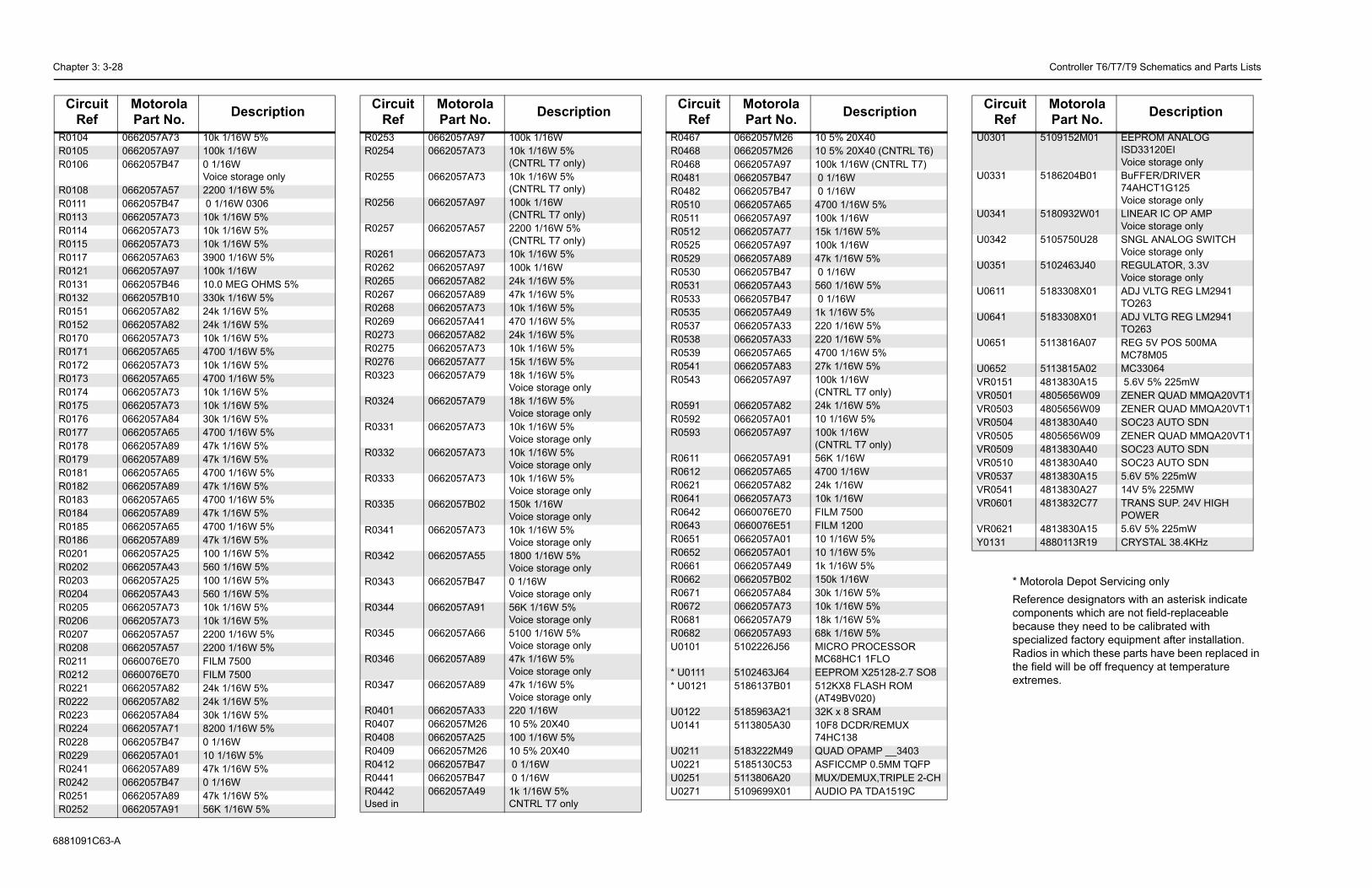
Chapter 3: 3-28 Controller T6/T7/T9 Schematics and Parts Lists
688109
* Motorola Depot Servicing onlyReference designators with an asterisk indicate components which are not field-replaceable because they need to be calibrated with specialized factory equipment after installation. Radios in which these parts have been replaced in the field will be off frequency at temperature extremes.
R0104R0105R0106
R0108R0111R0113R0114R0115R0117R0121R0131R0132R0151R0152R0170R0171R0172R0173R0174R0175R0176R0177R0178R0179R0181R0182R0183R0184R0185R0186R0201R0202R0203R0204R0205R0206R0207R0208R0211R0212R0221R0222R0223R0224R0228R0229R0241R0242R0251R0252
CircR
% 20X40% 20X40 (CNTRL T6) 1/16W (CNTRL T7)16W16W 1/16W 5% 1/16W/16W 5%
1/16W/16W 5%
16W1/16W 5%16W16W 5%1/16W 5%1/16W 5% 1/16W 5%/16W 5%
1/16WRL T7 only)/16W 5%
/16W 5% 1/16WRL T7 only)
1/16W 1/16W /16W/16W 7500 1200
/16W 5%/16W 5%16W 5% 1/16W/16W 5%/16W 5%/16W 5%/16W 5%O PROCESSOR
8HC1 1FLOROM X25128-2.7 SO8X8 FLASH ROM 9BV020)x 8 SRAM DCDR/REMUX 138
D OPAMP __3403ICCMP 0.5MM TQFP/DEMUX,TRIPLE 2-CHIO PA TDA1519C
Description
U0301 5109152M01 EEPROM ANALOG ISD33120EIVoice storage only
U0331 5186204B01 BuFFER/DRIVER 74AHCT1G125Voice storage only
U0341 5180932W01 LINEAR IC OP AMPVoice storage only
U0342 5105750U28 SNGL ANALOG SWITCHVoice storage only
U0351 5102463J40 REGULATOR, 3.3VVoice storage only
U0611 5183308X01 ADJ VLTG REG LM2941 TO263
U0641 5183308X01 ADJ VLTG REG LM2941 TO263
U0651 5113816A07 REG 5V POS 500MA MC78M05
U0652 5113815A02 MC33064VR0151 4813830A15 5.6V 5% 225mWVR0501 4805656W09 ZENER QUAD MMQA20VT1VR0503 4805656W09 ZENER QUAD MMQA20VT1VR0504 4813830A40 SOC23 AUTO SDNVR0505 4805656W09 ZENER QUAD MMQA20VT1VR0509 4813830A40 SOC23 AUTO SDNVR0510 4813830A40 SOC23 AUTO SDNVR0537 4813830A15 5.6V 5% 225mWVR0541 4813830A27 14V 5% 225MWVR0601 4813832C77 TRANS SUP. 24V HIGH
POWER VR0621 4813830A15 5.6V 5% 225mWY0131 4880113R19 CRYSTAL 38.4KHz
Circuit Ref
Motorola Part No. Description
1C63-A
0662057A73 10k 1/16W 5%0662057A97 100k 1/16W0662057B47 0 1/16W
Voice storage only0662057A57 2200 1/16W 5%0662057B47 0 1/16W 03060662057A73 10k 1/16W 5%0662057A73 10k 1/16W 5%0662057A73 10k 1/16W 5%0662057A63 3900 1/16W 5%0662057A97 100k 1/16W0662057B46 10.0 MEG OHMS 5%0662057B10 330k 1/16W 5%0662057A82 24k 1/16W 5%0662057A82 24k 1/16W 5%0662057A73 10k 1/16W 5%0662057A65 4700 1/16W 5%0662057A73 10k 1/16W 5%0662057A65 4700 1/16W 5%0662057A73 10k 1/16W 5%0662057A73 10k 1/16W 5%0662057A84 30k 1/16W 5%0662057A65 4700 1/16W 5%0662057A89 47k 1/16W 5%0662057A89 47k 1/16W 5%0662057A65 4700 1/16W 5%0662057A89 47k 1/16W 5%0662057A65 4700 1/16W 5%0662057A89 47k 1/16W 5%0662057A65 4700 1/16W 5%0662057A89 47k 1/16W 5%0662057A25 100 1/16W 5%0662057A43 560 1/16W 5%0662057A25 100 1/16W 5%0662057A43 560 1/16W 5%0662057A73 10k 1/16W 5%0662057A73 10k 1/16W 5%0662057A57 2200 1/16W 5%0662057A57 2200 1/16W 5%0660076E70 FILM 75000660076E70 FILM 75000662057A82 24k 1/16W 5%0662057A82 24k 1/16W 5%0662057A84 30k 1/16W 5%0662057A71 8200 1/16W 5%0662057B47 0 1/16W0662057A01 10 1/16W 5%0662057A89 47k 1/16W 5%0662057B47 0 1/16W0662057A89 47k 1/16W 5%0662057A91 56K 1/16W 5%
uit ef
Motorola Part No. Description
R0253 0662057A97 100k 1/16WR0254 0662057A73 10k 1/16W 5%
(CNTRL T7 only)R0255 0662057A73 10k 1/16W 5%
(CNTRL T7 only)R0256 0662057A97 100k 1/16W
(CNTRL T7 only)R0257 0662057A57 2200 1/16W 5%
(CNTRL T7 only)R0261 0662057A73 10k 1/16W 5%R0262 0662057A97 100k 1/16WR0265 0662057A82 24k 1/16W 5%R0267 0662057A89 47k 1/16W 5%R0268 0662057A73 10k 1/16W 5%R0269 0662057A41 470 1/16W 5%R0273 0662057A82 24k 1/16W 5%R0275 0662057A73 10k 1/16W 5%R0276 0662057A77 15k 1/16W 5%R0323 0662057A79 18k 1/16W 5%
Voice storage onlyR0324 0662057A79 18k 1/16W 5%
Voice storage onlyR0331 0662057A73 10k 1/16W 5%
Voice storage onlyR0332 0662057A73 10k 1/16W 5%
Voice storage onlyR0333 0662057A73 10k 1/16W 5%
Voice storage onlyR0335 0662057B02 150k 1/16W
Voice storage onlyR0341 0662057A73 10k 1/16W 5%
Voice storage onlyR0342 0662057A55 1800 1/16W 5%
Voice storage onlyR0343 0662057B47 0 1/16W
Voice storage onlyR0344 0662057A91 56K 1/16W 5%
Voice storage onlyR0345 0662057A66 5100 1/16W 5%
Voice storage onlyR0346 0662057A89 47k 1/16W 5%
Voice storage onlyR0347 0662057A89 47k 1/16W 5%
Voice storage onlyR0401 0662057A33 220 1/16WR0407 0662057M26 10 5% 20X40R0408 0662057A25 100 1/16W 5%R0409 0662057M26 10 5% 20X40R0412 0662057B47 0 1/16WR0441 0662057B47 0 1/16WR0442Used in
0662057A49 1k 1/16W 5%CNTRL T7 only
Circuit Ref
Motorola Part No. Description
R0467 0662057M26 10 5R0468 0662057M26 10 5R0468 0662057A97 100kR0481 0662057B47 0 1/R0482 0662057B47 0 1/R0510 0662057A65 4700R0511 0662057A97 100kR0512 0662057A77 15k 1R0525 0662057A97 100kR0529 0662057A89 47k 1R0530 0662057B47 0 1/R0531 0662057A43 560 R0533 0662057B47 0 1/R0535 0662057A49 1k 1/R0537 0662057A33 220 R0538 0662057A33 220 R0539 0662057A65 4700R0541 0662057A83 27k 1R0543 0662057A97 100k
(CNTR0591 0662057A82 24k 1R0592 0662057A01 10 1R0593 0662057A97 100k
(CNTR0611 0662057A91 56K R0612 0662057A65 4700R0621 0662057A82 24k 1R0641 0662057A73 10k 1R0642 0660076E70 FILMR0643 0660076E51 FILMR0651 0662057A01 10 1R0652 0662057A01 10 1R0661 0662057A49 1k 1/R0662 0662057B02 150kR0671 0662057A84 30k 1R0672 0662057A73 10k 1R0681 0662057A79 18k 1R0682 0662057A93 68k 1U0101 5102226J56 MICR
MC6* U0111 5102463J64 EEP* U0121 5186137B01 512K
(AT4U0122 5185963A21 32K U0141 5113805A30 10F8
74HCU0211 5183222M49 QUAU0221 5185130C53 ASFU0251 5113806A20 MUXU0271 5109699X01 AUD
Circuit Ref
Motorola Part No.
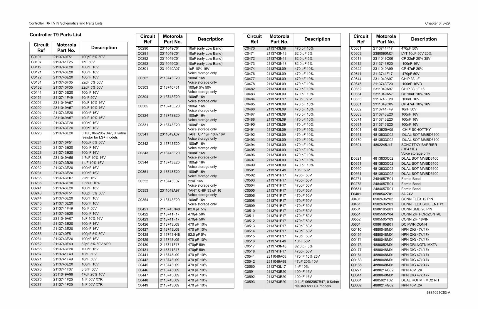
C Chapter 3: 3-29
6881091C63-A
C
470 pF 10%82.0 pF 5%82.0 pF 5%82.0 pF 5%470 pF 10%470 pF 10%470 pF 10%470 pF 10%470 pF 10%470 pF 10%470pF 50V470 pF 10%470 pF 10%470 pF 10%470 pF 10%470 pF 10%470 pF 10%470 pF 10%470 pF 10%470 pF 10%470 pF 10%470 pF 10%470 pF 10%470 pF 10%10nF 50V470pF 50V 470pF 50V 470pF 50V470pF 50V470pF 50V 470pF 50V 470pF 50V 470pF 50V470pF 50V 470pF 50V 470pF 50V470pF 50V 470pF 50V10nF 50V82.0 pF 5%470pF 50V 470nF 10% 25V47uF 20% 10V1nF 10%100nF 16V100nF 16V0.1uF, 0662057B47, 0 Kohm resistor for LS+ models
Description
C0601 2113741F17 470pF 50VC0603 2380090M24 LYT 10uF 50V 20%C0611 2311049C06 CP 22uF 20% 35VC0612 2113743E20 100nF 16VC0622 2311049A99 CP 47uF 20%C0641 2113741F17 470pF 50VC0644 2311049A97 CHIP 33 uFC0645 2113743E20 100nF 16VDC0652 2311049A97 CHIP 33 uF 16C0654 2311049A57 CP 10uF 10% 16VC0655 2113743E20 100nF 16VC0661 2311049C05 CP 47uF 10% 16VC0662 2113741F49 10nF 50VC0663 2113743E20 100nF 16VC0671 2113743E20 100nF 16VC0681 2113743E20 100nF 16VD0101 4813825A05 CHIP SCHOTTKYD0151 4813833C02 DUAL SOT MMBD6100D0179 4813833C02 DUAL SOT MMBD6100D0301 4802245J47 SCHOTTKY BARRIER
(RB471E) Voice storage only
D0621 4813833C02 DUAL SOT MMBD6100D0651 4813833C02 DUAL SOT MMBD6100D0660 4813833C02 DUAL SOT MMBD6100D0661 4813833C02 DUAL SOT MMBD6100E0271 2484657R01 Ferrite BeadE0272 2484657R01 Ferrite BeadE0631 2484657R01 Ferrite BeadF0401 6580542Z01 3A 24VJ0401 0902636Y02 CONN FLEX 12 PINJ0451 0902636Y01 CONN FLEX SIDE ENTRYJ0501 0986105B01 CONN SMD 20 PINJ0551 0905505Y04 CONN ZIF HORIZONTALJ0552 0905505Y03 CONN ZIF 18PINJ0601 0986165B01 DC PWR CONNQ0110 4880048M01 NPN DIG 47k/47kQ0151 4880048M01 NPN DIG 47k/47kQ0171 4880048M01 NPN DIG 47k/47kQ0173 4880052M01 NPN DRLNGTN MXTAQ0177 4880048M01 NPN DIG 47k/47kQ0181 4880048M01 NPN DIG 47k/47kQ0183 4880048M01 NPN DIG 47k/47kQ0185 4880048M01 NPN DIG 47k/47kQ0271 4880214G02 NPN 40V .2AQ0641 4880048M01 NPN DIG 47k/47kQ0661 4805921T02 DUAL ROHM FMC2 RHQ0662 4880214G02 NPN 40V .2A
Circuit Ref
Motorola Part No. Description
ontroller T6/T7/T9 Schematics and Parts Lists
ontroller T9 Parts List
Circuit Ref
Motorola Part No. Description
C0101 2113740F51 100pF 5% 50VC0107 2113741F25 1nF 50VC0112 2113743E20 100nF 16VC0121 2113743E20 100nF 16VC0122 2113743E20 100nF 16VC0131 2113740F35 22pF 5% 50VC0132 2113740F35 22pF 5% 50VC0141 2113743E20 100nF 16VC0151 2113741F49 10nF 50VC0201 2311049A57 10uF 10% 16VC0202 2311049A57 10uF 10% 16VC0204 2113743E20 100nF 16VC0212 2311049A57 10uF 10% 16VC0221 2113743E20 100nF 16VC0222 2113743E20 100nF 16VC0223 2113743E20 0.1uF, 0662057B47, 0 Kohm
resistor for LS+ modelsC0224 2113740F51 100pF 5% 50VC0225 2113743E20 100nF 16VC0226 2113743E20 100nF 16VC0228 2311049A56 4.7uF 10% 16VC0231 2113743B29 1 uF 10% 16VC0232 2113743E20 100nF 16VC0234 2113743E20 100nF 16VC0235 2113743E07 22nF 16V C0236 2113743E10 .033uF 10%C0241 2113743E20 100nF 16VC0243 2113740F51 100pF 5% 50VC0244 2113743E20 100nF 16VC0245 2113743E20 100nF 16VC0246 2113741F49 10nF 50VC0251 2113743E20 100nF 16V C0252 2311049A07 1uF 10% 16VC0254 2113743E20 100nF 16VC0255 2113743E20 100nF 16VC0256 2113740F51 100pF 5% 50VC0261 2113743E20 100nF 16VC0262 2113740F49 82pF 5% 50V NP0C0265 2113743E20 100nF 16VC0267 2113741F49 10nF 50VC0271 2113741F49 10nF 50VC0272 2113743E20 100nF 16VC0273 2113741F37 3.3nF 50VC0275 2311049A99 47uF 20% 10VC0276 2113741F25 1nF 50V X7RC0277 2113741F25 1nF 50V X7R
C0290 2311049C01 10uF (only Low Band)C0291 2311049C01 10uF (only Low Band)C0292 2311049C01 10uF (only Low Band)C0293 2311049C01 10uF (only Low Band)C0301 2311049A07 1uF 10% 16V
Voice storage onlyC0302 2113743E20 100nF 16V
Voice storage onlyC0303 2113740F51 100pF 5% 50V
Voice storage onlyC0304 2113743E20 100nF 16V
Voice storage onlyC0305 2113743E20 100nF 16V
Voice storage onlyC0324 2113743E20 100nF 16V
Voice storage onlyC0331 2113743E20 100nF 16V
Voice storage onlyC0341 2311049A07 TANT CP 1uF 10% 16V
Voice storage onlyC0342 2113743E20 100nF 16V
Voice storage onlyC0343 2113743E20 100nF 16V
Voice storage onlyC0344 2113743E20 100nF 16V
Voice storage onlyC0351 2113743E20 100nF 16V
Voice storage onlyC0352 2113743E07 22nF 16V
Voice storage onlyC0353 2311049A97 TANT CHIP 33 uF 16
Voice storage onlyC0354 2113743E20 100nF 16V
Voice storage onlyC0421 2113743N48 82.0 pF 5%C0422 2113741F17 470pF 50VC0423 2113741F17 470pF 50VC0426 2113743L09 470 pF 10%C0427 2113743L09 470 pF 10%C0428 2113743N48 82.0 pF 5% C0429 2113743L09 470 pF 10%C0430 2113741F17 470pF 50VC0431 2113741F17 470pF 50VC0441 2113743L09 470 pF 10%C0442 2113743L09 470 pF 10%C0445 2113743L09 470 pF 10%C0446 2113743L09 470 pF 10%C0447 2113743L09 470 pF 10%C0448 2113743L09 470 pF 10%C0449 2113743L09 470 pF 10%
Circuit Ref
Motorola Part No. Description
C0470 2113743L09C0471 2113743N48C0472 2113743N48C0473 2113743N48C0474 2113743L09C0476 2113743L09C0477 2113743L09C0478 2113743L09C0482 2113743L09C0483 2113743L09C0484 2113741F17C0485 2113743L09C0486 2113743L09C0487 2113743L09C0488 2113743L09C0490 2113743L09C0491 2113743L09C0492 2113743L09C0493 2113743L09C0494 2113743L09C0495 2113743L09C0496 2113743L09C0497 2113743L09C0499 2113743L09C0501 2113741F49C0502 2113741F17C0503 2113741F17C0504 2113741F17C0505 2113741F17C0506 2113741F17C0508 2113741F17C0509 2113741F17C0510 2113741F17C0511 2113741F17C0512 2113741F17C0513 2113741F17C0514 2113741F17C0515 2113741F17C0516 2113741F49C0517 2113743N48C0518 2113741F17C0541 2311049A05C0542 2311049A99C0560 2113743L17C0591 2113743E20C0592 2113743E20C0593 2113743E20
Circuit Ref
Motorola Part No.
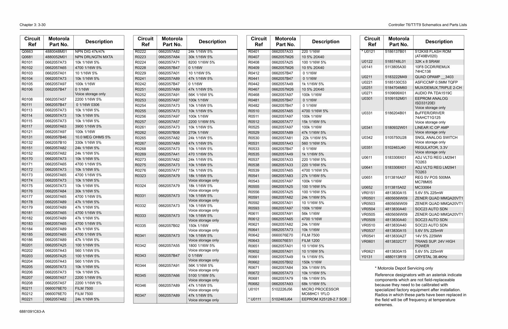
Chapter 3: 3-30 Controller T6/T7/T9 Schematics and Parts Lists
688109
* Motorola Depot Servicing onlyReference designators with an asterisk indicate components which are not field-replaceable because they need to be calibrated with specialized factory equipment after installation. Radios in which these parts have been replaced in the field will be off frequency at temperature extremes.
Q0663Q0681R0101R0102R0103R0104R0105R0106
R0108R0111R0113R0114R0115R0117R0121R0131R0132R0151R0152R0170R0171R0172R0173R0174R0175R0176R0177R0178R0179R0181R0182R0183R0184R0185R0186R0201R0202R0203R0204R0205R0206R0207R0208R0211R0212R0221
CircR
16W 20X4016W 5% 20X40WW
6W 5% 20X40/16WWW/16W 5%/16W
16W 5%/16W
16W 5%/16W 5%16W 5%W
6W 5%16W 5%16W 5%/16W 5%
16W 5%/16W16W 5%16W 5%16W 5%6W 5%/16W
16W/16W
16W16W 500200
6W 5%6W 5%6W 5%/16W
16W 5%16W 5%16W 5%16W 5%
PROCESSOR HC1 1FLOOM X25128-2.7 SO8
Description
* U0121 5186137B01 512KX8 FLASH ROM (AT49BV020)
U0122 5185748L01 32K x 8 SRAMU0141 5113805A30 10F8 DCDR/REMUX
74HC138U0211 5183222M49 QUAD OPAMP __3403U0221 5185130C53 ASFICCMP 0.5MM TQFPU0251 5184704M60 MUX/DEMUX,TRIPLE 2-CHU0271 5109699X01 AUDIO PA TDA1519CU0301 5109152M01 EEPROM ANALOG
ISD33120EIVoice storage only
U0331 5186204B01 BuFFER/DRIVER 74AHCT1G125Voice storage only
U0341 5180932W01 LINEAR IC OP AMPVoice storage only
U0342 5105750U28 SNGL ANALOG SWITCHVoice storage only
U0351 5102463J40 REGULATOR, 3.3VVoice storage only
U0611 5183308X01 ADJ VLTG REG LM2941 TO263
U0641 5183308X01 ADJ VLTG REG LM2941 TO263
U0651 5113816A07 REG 5V POS 500MA MC78M05
U0652 5113815A02 MC33064VR0151 4813830A15 5.6V 5% 225mWVR0501 4805656W09 ZENER QUAD MMQA20VT1VR0503 4805656W09 ZENER QUAD MMQA20VT1VR0504 4813830A40 SOC23 AUTO SDNVR0505 4805656W09 ZENER QUAD MMQA20VT1VR0509 4813830A40 SOC23 AUTO SDNVR0510 4813830A40 SOC23 AUTO SDNVR0537 4813830A15 5.6V 5% 225mWVR0541 4813830A27 14V 5% 225MWVR0601 4813832C77 TRANS SUP. 24V HIGH
POWER VR0621 4813830A15 5.6V 5% 225mWY0131 4880113R19 CRYSTAL 38.4KHz
Circuit Ref
Motorola Part No. Description
1C63-A
4880048M01 NPN DIG 47k/47k4880052M01 NPN DRLNGTN MXTA0662057A73 10k 1/16W 5%0662057A65 4700 1/16W 5%0662057A01 10 1/16W 5%0662057A73 10k 1/16W 5%0662057A97 100k 1/16W0662057B47 0 1/16W
Voice storage only0662057A57 2200 1/16W 5%0662057B47 0 1/16W 03060662057A73 10k 1/16W 5%0662057A73 10k 1/16W 5%0662057A73 10k 1/16W 5%0662057A63 3900 1/16W 5%0662057A97 100k 1/16W0662057B46 10.0 MEG OHMS 5%0662057B10 330k 1/16W 5%0662057A82 24k 1/16W 5%0662057A82 24k 1/16W 5%0662057A73 10k 1/16W 5%0662057A65 4700 1/16W 5%0662057A73 10k 1/16W 5%0662057A65 4700 1/16W 5%0662057A73 10k 1/16W 5%0662057A73 10k 1/16W 5%0662057A84 30k 1/16W 5%0662057A65 4700 1/16W 5%0662057A89 47k 1/16W 5%0662057A89 47k 1/16W 5%0662057A65 4700 1/16W 5%0662057A89 47k 1/16W 5%0662057A65 4700 1/16W 5%0662057A89 47k 1/16W 5%0662057A65 4700 1/16W 5%0662057A89 47k 1/16W 5%0662057A25 100 1/16W 5%0662057A43 560 1/16W 5%0662057A25 100 1/16W 5%0662057A43 560 1/16W 5%0662057A73 10k 1/16W 5%0662057A73 10k 1/16W 5%0662057A57 2200 1/16W 5%0662057A57 2200 1/16W 5%0660076E70 FILM 75000660076E70 FILM 75000662057A82 24k 1/16W 5%
uit ef
Motorola Part No. Description
R0222 0662057A82 24k 1/16W 5%R0223 0662057A84 30k 1/16W 5%R0224 0662057A71 8200 1/16W 5%R0228 0662057B47 0 1/16WR0229 0662057A01 10 1/16W 5%R0241 0662057A89 47k 1/16W 5%R0242 0662057B47 0 1/16WR0251 0662057A89 47k 1/16W 5%R0252 0662057A91 56K 1/16W 5%R0253 0662057A97 100k 1/16WR0254 0662057A73 10k 1/16W 5%R0255 0662057A73 10k 1/16W 5%R0256 0662057A97 100k 1/16WR0257 0662057A57 2200 1/16W 5%R0261 0662057A73 10k 1/16W 5%R0262 0662057B08 270k 1/16WR0265 0662057A82 24k 1/16W 5%R0267 0662057A89 47k 1/16W 5%R0268 0662057A73 10k 1/16W 5%R0269 0662057A41 470 1/16W 5%R0273 0662057A82 24k 1/16W 5%R0275 0662057A73 10k 1/16W 5%R0276 0662057A77 15k 1/16W 5%R0323 0662057A79 18k 1/16W 5%
Voice storage onlyR0324 0662057A79 18k 1/16W 5%
Voice storage onlyR0331 0662057A73 10k 1/16W 5%
Voice storage onlyR0332 0662057A73 10k 1/16W 5%
Voice storage onlyR0333 0662057A73 10k 1/16W 5%
Voice storage onlyR0335 0662057B02 150k 1/16W
Voice storage onlyR0341 0662057A73 10k 1/16W 5%
Voice storage onlyR0342 0662057A55 1800 1/16W 5%
Voice storage onlyR0343 0662057B47 0 1/16W
Voice storage onlyR0344 0662057A91 56K 1/16W 5%
Voice storage onlyR0345 0662057A66 5100 1/16W 5%
Voice storage onlyR0346 0662057A89 47k 1/16W 5%
Voice storage onlyR0347 0662057A89 47k 1/16W 5%
Voice storage only
Circuit Ref
Motorola Part No. Description
R0401 0662057A33 220 1/R0407 0662057M26 10 5%R0408 0662057A25 100 1/R0409 0662057M26 10 5%R0412 0662057B47 0 1/16R0441 0662057B47 0 1/16R0442 0662057A49 1k 1/1R0467 0662057M26 10 5%R0468 0662057A97 100k 1R0481 0662057B47 0 1/16R0482 0662057B47 0 1/16R0510 0662057A65 4700 1R0511 0662057A97 100k 1R0512 0662057A77 15k 1/R0525 0662057A97 100k 1R0529 0662057A89 47k 1/R0530 0662057A81 22k 1R0531 0662057A43 560 1/R0533 0662057B47 0 1/16R0535 0662057A49 1k 1/1R0537 0662057A33 220 1/R0538 0662057A33 220 1/R0539 0662057A65 4700 1R0541 0662057A83 27k 1/R0543 0662057A97 100k 1R0555 0662057A25 100 1/R0556 0662057A25 100 1/R0591 0662057A82 24k 1/R0592 0662057A01 10 1/1R0593 0662057A97 100k 1R0611 0662057A91 56k 1/R0612 0662057A65 4700 1R0621 0662057A82 24k 1/R0641 0662057A73 10k 1/R0642 0660076E70 FILM 7R0643 0660076E51 FILM 1R0651 0662057A01 10 1/1R0652 0662057A01 10 1/1R0661 0662057A49 1k 1/1R0662 0662057B02 150k 1R0671 0662057A84 30k 1/R0672 0662057A73 10k 1/R0681 0662057A79 18k 1/R0682 0662057A93 68k 1/U0101 5102226J56 MICRO
MC68* U0111 5102463J64 EEPR
Circuit Ref
Motorola Part No.

Controller T11 Schematics and Parts Lists Chapter 3: 3-31
6881091C63-A
5
C065233uF
R067130K
10KR0672
C0671
0.1uF
D0621
RESET
RESET
1
VR0621
GN
DG
ND
4
INPUT2
2NP
NC1
3
NC25
NC36
NC478
NC5
U0652MC33064
2
GN
D
1IN OUT
3
MC78M05U0651
0.1uF
C0651 C0655
NU0.1uF
470pFNU
C0621
47uFC0622
VR0671NU
Q0681
R068268K
R068118K
0.1uFC0681
R0621
24K
MC33464N-45ATRU0653
NU
10uF
9V3
FLT_A+
IN_5V_RF_REG
RESET
5VD
C0654
BATTERY_VOLTAGE
EXT_SWB+
INT_SWB+
PASUPVLTG
VSTBY
FL0830679O
Controller T11 Schematic Diagram - Supply Voltage
.0 Controller T11 Schematics and Parts Lists
10
22uF
C0611
R0651
R06124.7K
D0661
Q0662
VIN4
VOUT5
LM2941
U0611
ADJ1
GN
D1
3
GN
D2
6
2ON_OFF
10K
47K
47K
R0641
J0601-1
.01uFC0662
R0662150K Q0663
47K
47K
C0603
R0661
1K
10uF
TP0661
C06630.1uF
R06431.2K
0.1uF
C0645
VR0601
4 VIN 5VOUT
U0641
LM2941
1ADJ
GN
D1
3
GN
D2
6
ON_OFF2
Q0661
R061156K
57R01E0631
470pFC0601
47uFC0661
R06427.5K470pF
C0641C0644
33uF
D0651
J0601-2
C0612
0.1uF
J0601-3
D0660
R0652
10Q0641
DC_POWER_ON
IGNITION_CONTROL
EMERGENCY_CONTROL
ON_OFF_CONTROL
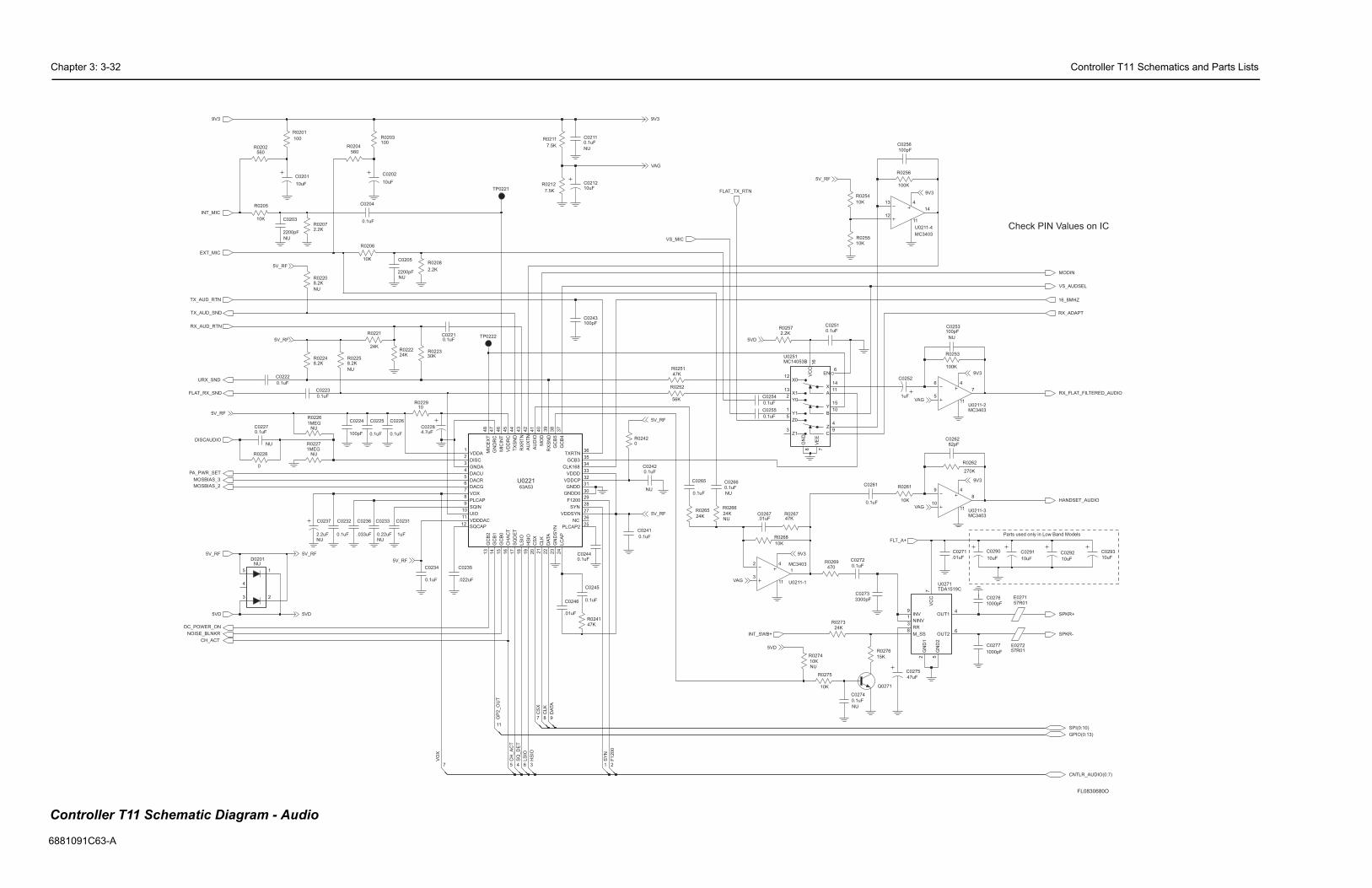
Chapter 3: 3-32 Controller T11 Schematics and Parts Lists
6881091
Check PIN Values on IC
F1
6
5
7
4
11U0211-2MC3403
4
5
1
0
C0275
47uF
4K0273
12
14
4
11
U0211-4
MC3403
13
C0271
.01uF
100pF
C0256
R0256
100K
10K
R0254
10K
R0255
57R01E0272
15K
1000pF
R0276
7V
CC C0276
GN
D1
GN
D2
5
9INV
8M_SS
1NINV
4OUT1
6OUT2
RR3
TDA1519CU0271
2
10K
R0261
0.1uF
C0274
NU
9
10
8
4
11 U0211-3MC3403
100K
R0253
100pFC0253
NU
1uF
C0252
C0291
10uF
C0290
10uF 10uFC0292
10uF
C0293
0.1uF
C0261
C0273
3300pF
Q0271
C0272
0.1uF
C026282pF
9
270K
R0262
C0277
1000pF
57R01E0271
RX_ADAPT
9V3
9V3
MODIN
16_8MHZ
SPKR-
FLT_A+
SPKR+
9V3
VS_AUDSEL
SPI(0:10)
GPIO(0:13)
CNTLR_AUDIO(0:7)
VAG
VAG
HANDSET_AUDIO
RX_FLAT_FILTERED_AUDIO
Parts used only in Low Band Models
FL0830680O
Contr
C63-A
LS
IO
F1200
SY
N
CL
K
GP
2_O
UT
CS
X
DA
TA
VO
X
CH
_A
CT
HS
IO
SQ
_D
ET
4
0.1uC025
C0255
0.1uF
1
1
VDDCP32
VDDD33
VDDDAC
SQCAP
11
12
VD
DR
C45
VDDSYN27
VOX7
SQ
DE
T17
SQIN9
SYN28
TXRTN36T
XS
ND
44
UIO10
VDDA
LS
IO18
MIC
EX
T48
MIC
INT
46
MO
D40
NC26
PLCAP8
PLCAP225
GC
B5
RX
SN
D
AU
XT
N
RX
RT
N
38
39
GNDA3
GNDD
GNDD0
31
30G
ND
RC
47
GN
DS
YN
23
HS
IO19
24
LC
AP
DA
TA
22
DISC2
F120029
GC
B0
15
GC
B1
14
GC
B2
13
GCB335
37
GC
B4
CH
AC
T16
CL
K21
CLK16834
CS
X20
DACG6
DACR5
4DACU
63A53
U0221
AU
DIO
41
42
43
R0206
10K C0205
2200pFNU
0.1uFC0266
NU
C0267
C0231
1uF
.01uF
11
Y11
Z4
Z05
3Z1
GN
D8
VC
C16
VE
E7
X1
X012
X113
Y1
Y02
U0251
1A
B1
C9
EN6
R0208
2.2K
6
MC14053B
NU
C02110.1uF
NU
9
R0266
24K
C0224
100pF
C0237
2.2uFNU
47KR0267
10K
R0268
10uF
C0202
10uF C0212
0.1uF
C0225
2R
10uF
C0201
23
8
NU
8.2KR0225
8.2KR0224
100pFC0243
R0242
0.1uF
NU
0
C0242
560
C0244
R0204
C0235
0.1uF
.022uF
47KR0241
.01uF
C0246
0.1uF
C0241
TP0221
8.2KR0220
NU
C0245
0.1uF
100R0203
C0233
0.22uFNU
C0232
0.1uF
R02271MEG
NU
5
0.1uF
C0222
7
NU
R02072.2K
R0226
1MEG
0.1uF
NU
C0227
C0221
0.1uF
0.1uF
R0252C0223
56K
30KR0223
R0212
R0211
7.5K
C0236
7.5K
.033uF
R0265
24K
C0265
0.1uF
NU
5
3
1
2
4
D0201
0.1uF
C0254
C0234
7
0.1uF
TP0222
47K
R0251
2.2KR0257
C02284.7uF
10K
R0275
R0228
0
560R0202
R022224K
0.1uF
C0226
470
NU
R026
2200pF
C0203
10R0229
0.1uF
C0204
R0221
24K
U0211-1
MC34032
3
1
4
11
R0274
NU10K
R0201
R0205
100
5V_RF5V_RF
TX_AUD_RTN
5V_RF
TX_AUD_SND
5V_RF
DISCAUDIO
5V_RF
5V_RF
FLAT_TX_RTN
10K
INT_SWB+
CH_ACT
VAG
9V3 9V3
9V3
VS_MIC
MOSBIAS_3
VAG
EXT_MIC
5V_RF
5V_RF
5VD5VD
5V_RF
RX_AUD_RTN
INT_MIC
URX_SND
FLAT_RX_SND
DC_POWER_ON
5VD
5VD
PA_PWR_SET
MOSBIAS_2
NOISE_BLNKR
oller T11 Schematic Diagram - Audio

Controller T11 Schematics and Parts Lists Chapter 3: 3-33
6881091C63-A
DIG_IN_OUT_4
9
18
GM300
SPEAKER-
13
J0501
DIG_IN_6 WITH WAKEUP (IGNITION)FLAT/FILTERED_RX_AUDIO
1
PCB
8
34
11
DIG_IN1
DIG_IN_OUT_8SWB+
14
2
10
6
15 17
6
RSSI
NC
BOOT_CNTRL
20
TO/FROM RF
3
ACCESSORY
12
20
REAR VIEW
15
16
7
DIG_OUT2 (EXTERNAL_ALARM)
1110
SPEAKER+BUS+
NC
17
GROUND
14
4
5
13DIG_IN_OUT_7
2 8
5
16
DIG_IN_3
DIG_IN_5 WITH WAKEUP (EMERGENCY)
1
20-PIN CONNECTOR
FLAT_TX_AUDIO
7
9
12
19
18
19WARI S
TO/FROM RF
EXT_MIC_AUDIO
PA_PWR_SET
PASUPVLTG
_1
J0501-16
MODIN
J0501-3
J0501-20
J0501-17
16_8MHZ_CNTLR_1
J0501-5
C0495470pF
DISCAUDIO
1
J0501-4
J0501-14
PA_PWR_SET_1_CNTLR_1
NOISE_BLNKR_CNTLR_1
470pFC0497
DISCAUDIO_CNTLR_1
MODIN_CNTLR_1
J0501-2
J0501-11
J0501-12
DATA
J0501-15
470pFC0494
CLK
MOSBIAS_2_CNTLR_1
IN_5V_RF_REG_CNTLR_1
TEMPSENSE
RESET
5V
IN_5V_RF_REG
J0501-8
J0501-1
5V_CNTLR_1
MOSBIAS_3
C0493470pF
DATA
CSX
J0501-13
CLK
J0501-9
470pF
CNTLVLTG
C0491_1
J0501-6
TP0492 TP0497
INT_SWB
LOCK
RSSI
MOSBIAS_3_CNTLR_1MOSBIAS_2
J0501-10
C0490
9V3
470pFC0492470pF
J0501-19
C0496470pF 470pF
C0499
NOISE_BLNKR
INT_SWB_CNTLR_1
J0501-7
J0501-18
16_8MHZ
CSX
T_ACC8
Q
N
GP6_IN_ACC10GP6_IN_ACC10
10
3
DISCAUDIO
MODIN
INT_MIC INT_MIC
SPKR+SPKR+DISCAUDIO ISCAUDIO
HANDSET_AUDIO
RSSI RSSI
IN_5V_RF_REG
GP1_IN_ACC3 GP1_IN_ACC3
INT_SWB+
EXP_BD_REQEXP_BD_REQ
CH_ACT CH_ACT
RDYRDY
OPT_PTTOPT_PTT
NOISE_BLNKR
MOSBIAS_2
PA_PWR_SET
FLAT_TX_RTN FLAT_TX_RTN
GP4_IN_OUT_ACC8 GP4_IN_OUT_ACC8
MOSBIAS_3
VS_MIC VS_MIC
BUS+ BUS+RESETRESET
ON_OFF_CONTROL ON_OFF_CONTROL
16_8MHZ
5V_RF
5VD5VDFLT_A+
EXT_MICEXT_MIC
SPKR-SPKR-FLT_A+
HANDSET_AUDIO
ZWG0131050-O
Controller T11 Schematic Diagram - I/O
R/W*
SPI_MOSI
NC
NC
7
CLK
9
Fuse P/N6580542Z01
CS*
24
DISCAUDIO
NC
BUS+10
9V3
VS_MIC
13
2GND
5
DATA
CLK
30
J0451
1514
16
23
21
SPI_CLK
35
OFF_BATT_DATA_OUTVS_GAINSEL
Gnd
DB2
3
EXP1_CS
56
SPEAKER-
Rdy/Req
GROUND
19
9
VS_CS
RDY
EXT_BD_REQEXT_BD_CS
12
2
6
NC
1
121314
15
40
18-PIN CONNECTORRS232 INTERFACE BOARD
GND
BUS+
5
NC
GND
J0552
NC
GROUNDGROUND
GROUND
DB1
22
GP4_IN_OUT
DATA
SCK_Snd
FAST_SQ
EXT_BD_PTT
GND
EXP_BD_REQ
NC
NC
DB6
16
DB3
MISO
NC
910111213
EXT_BD_PTT
12
Rx_Aud_Rtn
31
4
12
18-PIN CONNECTOR
7
17
1
HANSET_AUDIO
Opt_Bd_En
6
11
17
NC
15161718
34
INTERNAL OPTION BOARD
3938
9
21
NC
CLK
4
11
J0551
28
FLT_A+
Key_Col
EXP2_CS
SPI_MISO
5VD
EXP2_CS
CONTROL HEADJ0401
5VD9V3
5VD
EXT_BD_PTT
13
Flat_Tx_Rtn
NC
12
SrD_Snd
11
10
11
1
14151617
4
NC
33
7
9
18
SrD_Rtn
NC
10
OPT_CS
VS_RAC
8
RST*
78
INT_EXT_Vdd
EXT_BD_PTT
Det_Aud_Snd
18
40-PIN CONNECTOR
DB5
EXP_BD_PTTGND
37
LED_EN
DATA
DIG_IN_6 WITHWAKEUP
CLK
Tx_Aud_Rtn
4
EXPANSION BOARD
OPT_PTT
20
SCI_TX
INT_MIC
Tx_Aud_Snd
Rx_Aud_SndON
VS_INT
5
Key_Row
Key_Intrp
3NC
NC
3
ON_OFF_CONTROL
3
OPT_CS
12-PIN CONNECTOR
DB7
RESET
FLT_A]
DISCAUDIOCH_ACT
DIG_IN_OUT_4
DATA
EXP1_CS
VS_AUDSEL
26
FLAT_TX_RTN
8
6
CSX29MISO
2
56
18
8
36
DB0
PTT
8
Vddd
25
32
EXT_BD_PTT
27
7
10
A04
VS_CS
DB4
EXP_BD_PTT
SPEAKER+
14
3
470pFC0513
TEMPSENSE_CNTLR
10
C0505470pF
J0551-8
VR0505
CLK_CNTLR_1
C0518470pF
VR0509
C0487470pF
C0431470pF
470pFC0423
470pFC0514
C05601000pF
J0401-11J0451-11
220R0401
J0551-11
C0488470pF
3A
F0401
470pF
47K
C0484
NU
R0542
VR0537
J0401-1
82pFC0517
CNTLVLTG_CNTLR_
9
J0551-3
J0551-10
470pFC0510
0.47uFC0541
J0551-40
10R0592
J0451-5
3
J0551-20
R0525100K
J0551-25
220R0538
VR0501
J0551-4
J0551-14
C0542
47uF
R0533
J0551-23
0
J0551-18
R0511100K
CSX_CNTLR_1
J0551-37
R0529
47K
J0551-19
J0551-41
J0451-1
J0551-36
J0551-32
R0530
22K
J0401-10
J0401-7
RSSI_CNTLR_1
R04410
470pF
NU470pFC0575
C0477
DATA_CNTLR_1
LOCK_CNTLR_1
0R0412
C0447470pF
J0551-22
J0451-10
470pFC0509
J0451-17
C047282pF
J0451-6
1
100KR0543
J0451-12
VR0510
J0401-5
NU470pF
C0559
470pFC0429
R051215K
C0426470pF
C0501.01uF
C0421
J0451-16
82pF
82pFC0473
J0401-4
J0551-21
J0401-9
J0401-3
J0401-8
J0451-18
8CLK_CNTLR_2
0.1uFC0591
C0516.01uF
J0451-4
R059124K
J0551-31
470pFC0512
J0551-42
470pFC0442
C0485
J0401-12
J0551-13
470pFC0483
9
470pF
J0551-27
VR0541
470pFC0441
80.1uFC0592
R0407
560
10
R0531
J0551-12
2
L0482
J0451-7
NU390nH
C0478470pF
J0551-15
R0408100
470pFC0511
7
R0539
J0551-29
4.7K
J0551-39
R05104.7K
NU
L0481390nH
C0506470pF
C0449470pF
1KR0442
4
TP0530
J0551-26
J0401-6
J0551-6
J0451-8
J0551-34
470pF
82pFC0471
C0422
0.1uFC0593
R0482 0
R0481 0
R0468100K
C0443470pF
J0551-17
NU
J0551-30
C0474470pF
J0451-9
100KR0593
VR0504
J0451-13
C0515470pF
DATA_CNTLR_2
C0503470pF
PASUPVLTG_CNTRL
J0401-2
VR0503
R0537220
J0451-15
470pFNU
C0558
10R0409
J0451-2
470pFC0508
J0551-35
J0451-14
J0551-1
J0551-28
R05351K
470pF
J0551-5
C0430
470pFC0486
RESET_CNTLR_1
CSX_CNTLR_2
C0476470pF
J0551-33
C0482470pF
NU
C0576470pF
9
9V3_CNTLR_1
C0554
J0451-3
NU0.1uF
J0551-24
10R0467
J0551-9
470pFC0427
J0551-2
J0551-16
C0470470pF
R054127K
470pFC0502
470pFC0504
0
R0509
470
R0508
J0551-7
J0551-38
8
C042882pF
C0448470pF
C0445470pF470pF
C0446
GP4_IN_OUOPT_CSRDYOPT_PTT
EXP2_CS
EXP_BD_RE
5VD
SPKR-SPKR+
ON_OFF_CONTROL
BUS+
BUS+
GP6_IN_ACC10
GP5_IN_ACC9
GP2_OUT_ACC4
GP7_IN_OUT_ACC12
GP8_IN_OUT_ACC14
SPKR+
GP3_IN_ACC6GP4_IN_OUT_ACC8
EXP2_CS
FLAT_TX_RT
FLAT_TX_RTN
GP6_IN_ACC
GP1_IN_ACC3
FLT_A+
CH_ACT
GP1_IN_ACCSPI_DATASPI_MISOSPI_CLK
EXP1_CS
9V3
SPI_MISO
CH_ACT
5VD9V3
5VDSPI_MISO
RESET
FLT_A+
DISCAUDIO
GP4_IN_OUT_ACC8EXP1_CS
EXP_BD_REQGP1_IN_ACC3
SPI_CLKSPI_DATA
SPKR-EXT_MIC
GP1_IN_ACC3
INT_MIC
HANDSET_AUDIO
BOOT_CNTRL
5VD
BUS+
GP4_IN_OUT_ACC8EXP1_CS
EXP_BD_REQGP1_IN_ACC3
CH_ACTDISCAUDIO
FLT_A+
SCI_TX
RX_FLAT_FILTERED_AUDIO
EMERGENCY_CONTROL
RSSI
EXT_SWB+
RDY
OPT_PTT
EXP1_CS
9V3
DISCAUDIO
SPI(0:10)
FLAT_TX_RTN
5VD
FLT_A+
SPI_DATA
SPI_CLK
SPI_MISO
VS_CS
OPT_CSRESET
RESET
PASUPVLTG
BUS+
TEMPSENSE
CNTLVLTG
RSSI
LOCK
OPT_CS
SPI_DATA
TX_AUD_RTN
VS_CSVS_MIC
SPI_CLK
FLAT_RX_SNDRX_AUD_RTN
URX_SND
TX_AUD_SND
VS_INT
5VDVS_AUDSEL
VS_GAINSELSPI_MISO
VS_RAC
IGNITION_CONTROL
FLT_A+
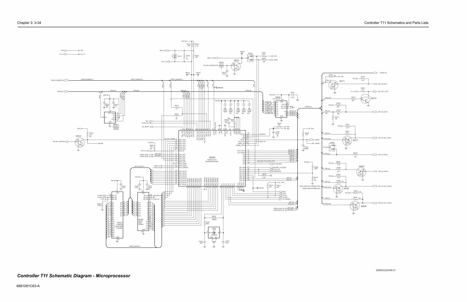
Chapter 3: 3-34 Controller T11 Schematics and Parts Lists
6881091
GP3_IN
GP8_IN
PE6
GP5_IN
HC138_A 2
HC138_A1
GP2_OUT
GP5_IN
HC138_A 1
R0105 USED IN STANDARD ONLY
GP8_OUT
HC138_A1
R0106 USED IN PRIME ONLY
NU
GP8_IN
GP4_IN
HC138_A0
GP3_IN
GP6_IN
GP6_IN
GP4_OUTGP7_OUT
HC138_A 0
GP1_IN
GP4_IN
GP8_OUTGP7_IN
GP1_IN
GP7_IN
GP4_OUT
GP7_OUT
4.7K
R0181
0R0106
Q0183
5
2
Q0171
47K
Q0177
R0186
R0176
5
30K
13
9
R0182
47K
R0105100K
R017847K
2
4.7K
R0171
R0183
4.7K8
D0179
2.2KR0108
R0177
4.7K
7
83
13
0
4.7K
12
R0173
6
4
3
6
47KR0184
R0174
10K
Q0185
R0179
47K
Q0173
1
7
0
12
6
S24
S35
A01
A12
A23
CS1
A
4.7KR0185
C01071000pF
Q0181
9
11
R017010K
4
10
C0141
0.1uF
R017210K
R0175
10K
10
1
5VD
GP1_IN_ACC3
GP6_IN_ACC10
GP2_OUT_ACC4
5VDIRQ
_RAC_INT
GP4_IN_OUT_ACC8
GP3_IN_ACC6
5VD
RESET
RESET
5VD
GP5_IN_ACC9
GPIO(0:13)
GPIO(0:13)
5VD
5VD
FLT_A+
_GAINSEL
SI
5VD
CK
GP7_IN_OUT_ACC12
GP8_IN_OUT_ACC14
5VD
5VD
5VD
5VD
GE
ZWG0131049-O
Contr
C63-A
LVZIF_CS
ON_OFF_SENSE
GP4_OUT
VS_CSEXP1_CS
SY
N
LSIO
MICROPROCESSOR
CLK CS
X
OPT_CS
32kx8bit
GP7_OUT
SQ
_DE
T
FLASH ROM
EE
_CS
HS
IO
EE_CS
512kx8bit
RAM
HS
IO
DA
TA
EEPROM
REF_CS
MIS
O
EXP2_CS
DA
TA
MIS
O
F12
00
VO
X
LSIO
CLK
CH
AC
T
16Kx8bit
(EXT_BD_PTT & DATA_PTT)
0
R0112
NU
0.1uFNU
8
10C0108
NU
R0103
C0111100pF
4.7KR0102
100pFNU
C0103
15
C013122pF
VR0151
14
9
7
0
2
1514 14
13
4
7
5
0.1uFC0112
100KR0121
0
3
10
6
13
4
0
0
6
1
2
NC3
NC1
4OUT
1IN
XTALY0131
38.40KHz
Q0110 NU
4
3
18
R011010K
16
5
4
R0131
10MEG
C0105100pFNU
4
D0101
16
5
R0117
3.9K
5
2
1
C0123100pFNU
11
R011310K
Q0151
IO 628
IO 729
8
VCC
2
EN_WE7
24
GND
21IO 0IO 1
22
IO 223
IO 325
IO 426
IO 527
A41615
A514
A6A7
13
A83
A92
EN_CE30
EN_OE32
4A13A14
511
A15A16
10
A176
A189
A218
A317
A020
A119
A1031
A111
A1212
23
3
U0121AT49F040
6
17
9
10K
5
7
R0101
3
8
TP0101
47KNU
6
R0107
1
4
1
17
7
109 9
C01220.1uF TP0103
3
11 1
103
2
1
0
CS1
HOLD7
SCK6
SI5
SO2
VCC
8
VSS
4
WP3
U0111X25128-2.7
12
24KR0151
12
013
4
D0151
3
1
2
8
2
6
10
65
1
87
TP0151
C0121
C0102
NU
0.1uF
100pF 100pFC0104
NU
18
22pFC0132
7
4
C0151.01uF
C0106
NU
100pF
12
Y411
Y510
Y69
Y77
3
EN_CEN_C
GND
8
VCC
16
Y015
Y114
Y213
Y3
EN_
65
12
U0141MC74HC138
10
TP0102
6
80
12IO 2
13IO 3
15IO 4
16IO 5
17IO 6
18IO 7
19IO 8
28
VCC
3A7
25A8
24A9
20EN_CS
22EN_OE
27EN_WE
GND
14
11IO 1
2A12
26A13
1A14
8A2
7A3
6A4A5
54
A6
63A21U0122
10A0
9A1
A102123
A11
11
10KR0114
R010410K
13V
SS
40V
SS
L
87V
SS
R
XF
C93
48XIRQ
91X
TA
L
PJ678
PJ7
94RESET
12V
DD
39V
DD
L
88V
DD
R
92V
DD
SY
N
69V
RH
68V
RL
PI6
49P
I7
71PJ0_CSGP3
72PJ1_CSGP4
73PJ2
74PJ3
75PJ4
76PJ5
77
PH6_CSGP238
PH7_CSPROG
56P
I0
55P
I1
54P
I2
53P
I3
52P
I4
51P
I5
50
4PG7_R_W
47PH0_PW1
46PH1_PW2
45PH2_PW3
44PH3_PW4
43PH4_CSIO
42PH5_CSGP1
41
PF
7_A
DD
R7
29P
FO
_AD
DR
0
6PG0_XA13
16PG1_XA14
20PG2_XA15
19PG3_XA16
17PG4_XA17
18PG5_XA18
5PG6_AS
PE7_AN760
28P
F1_
AD
DR
1
27P
F2_
AD
DR
2
26P
F3_
AD
DR
3
25P
F4_
AD
DR
4
24P
F5_
AD
DR
5
23P
F6_
AD
DR
6
22
PD
5_S
SP
D6_
LVIN
3
PE0_AN067
PE1_AN166
PE2_AN265
PE3_AN364
PE4_AN463
PE5_AN562
PE6_AN661
36PC6_DATA6
37PC7_DATA7
97P
D0_
RX
D
98P
D1_
TX
D
99P
D2_
MIS
O
100
PD
3_M
OS
I
1P
D4_
SC
K
2
PB
6_A
DD
R14
7P
B7_
AD
DR
15
14P
BO
_AD
DR
8
30PC0_DATA0
31PC1_DATA1
32PC2_DATA2
33PC3_DATA3
34PC4_DATA4
35PC5_DATA5
85P
A6_
OC
2_O
C1
86P
A7_
PA
1_O
C1
10P
B1_
AD
DR
9
11P
B2_
AD
DR
10
9P
B3_
AD
DR
11
21P
B4_
AD
DR
12
15P
B5_
AD
DR
13
8
95
58MODA_LIR
57MODB_VSTBY
79P
A0_
IC3
80P
A1_
IC2
81P
A2_
IC1
82P
A3_
IC4_
OC
5_O
C1
83P
A4_
OC
4_O
C1
84P
A5_
OC
3_O
C1
59A
VD
D
70A
VS
S
89ECLK
90E
XT
AL
96IRO
LVO
UT
U0101MC68HC11FL0
0
5
NU
R01160
24K
R0152
330KR0132
6
2
7
R011510K
R0111
0
7
C0101100pF
RAM_CS
BUS+
CNTLVLTG
SCI_TX
R_W
FLASH_CEFLASH_OE
IRQ
ADDR_BUS(0:18 )
DATA_BUS(0:7)
5VD
9
FROM_U0101_47
VS
5VD
VS
5VDBOOT_CNTRL
ON_OFF_CONTROL
R_W
5VD
5VD
5VD
OPT_PTT
5VD
SPI(0:10)SPI(0:10) SPI(0:10) SPI(0:10) SPI(0:10)
CNTLR_AUDIO(0:7) CNTLR_AUDIO(0:7)CNTLR_AUDIO(0:7)CNTLR_AUDIO(0:7)
FROM_U0101_47FROM_U0101_46
FROM_U0101_46
TEMPSENSE
RAM_CS
5VD
VS
EXT_BD_REQ
RS
RX_ADAPT
5VD
5VD5VD
FLT_A+ FLT_A+
FLASH_OE
NC
_XT
AL
ECLK
NC
NC
LO
RDY
ON_OFF_CONTROL
NC
FLASH_CE
R_W
VSTBY
5VD
BATTERY_VOLTA
oller T11 Schematic Diagram - Microprocessor

C Chapter 3: 3-35
6881091C63-A
C
CAP, 470pFCAP, 470pFCAP, 470pFCAP, .01uFCAP, 470pFCAP, 470pFCAP, 470pFCAP, 470pFCAP, 470pFCAP, 470pFCAP, 470pFCAP, 470pFCAP, 470pFCAP, 470pFCAP, 470pFCAP, 470pFCAP, 470pFCAP, .01uFCAP, 82pFCAP, 470pFCAP, 0.47uFCAP, 47uFCAP, 1000pFCAP, 0.1uFCAP, 0.1uFCAP, 0.1uFCAP, 470pFCAP, 10uFCAP, 22uFCAP, 0.1uFCAP, 47uFCAP, 470pFCAP, 33uFCAP, 0.1uFCAP, 33uFCAP, 10uFCAP, 0.1uFCAP, 47uFCAP, .01uFCAP, 0.1uFCAP, 0.1uFCAP, 0.1uFMMBD301MMBD6100
Description
D0179 4813833C02 MMBD6100D0621 4813833C02 MMBD6100D0651 4813833C02 MMBD6100D0660 4813833C02 MMBD6100D0661 4813833C02 MMBD6100E0271 2484657R01 FERRITE BEADE0272 2484657R01 FERRITE BEADE0631 2484657R01 FERRITE BEADF0401 6580542Z01 FUSEJ0401 0902636Y02 CONN, 12-PIN, CON-
TROL HEADJ0451 0902636Y01 CONN, 18-PIN, EXPAN-
SION BOARDJ0501 0986105B01 CONN, 20-PIN, ACCES-
SORYJ0551 0905505Y04 CONN, 40-PIN, INTER-
NAL OPTIONJ0552 0905505Y03 CONN, 18-PIN, RS232J0601 0986165B01 DC POWER CONNEC-
TORQ0110 4880048M01 DTC144EKAQ0151 4880048M01 DTC144EKAQ0171 4880048M01 DTC144EKAQ0173 4880052M01 RXT-A28Q0177 4880048M01 DTC144EKAQ0181 4880048M01 DTC144EKAQ0183 4880048M01 DTC144EKAQ0185 4880048M01 DTC144EKAQ0271 4880214G02 MMBT3904Q0641 4880048M01 DTC144EKAQ0661 4805921T02 FMC2AQ0662 4880214G02 MMBT3904Q0663 4880048M01 DTC144EKAQ0681 4880052M01 RXT-A28R0101 0662057A73 RES, 10KR0102 0662057A65 RES, 4.7KR0103 0662057A01 RES, 10R0104 0662057A73 RES, 10KR0105 0662057A97 RES, 100KR0108 0662057A57 RES, 2.2KR0111 0662057B47 RES, 0R0113 0662057A73 RES, 10KR0114 0662057A73 RES, 10KR0115 0662057A73 RES, 10K
Circuit Ref
Motorola Part No. Description
ontroller T11 Schematics and Parts Lists
ontroller T11 Parts List
Circuit Ref
Motorola Part No. Description
C0101 2113740F51 CAP, 100pFC0107 2113741F25 CAP, 1000pFC0112 2113743E20 CAP, 0.1uFC0121 2113743E20 CAP, 0.1uFC0122 2113743E20 CAP, 0.1uFC0131 2113740F35 CAP, 22pFC0132 2113740F35 CAP, 22pFC0141 2113743E20 CAP, 0.1uFC0151 2113741F49 CAP, .01uFC0201 2311049A57 CAP, 10uFC0202 2311049A57 CAP, 10uFC0204 2113743E20 CAP, 0.1uFC0212 2311049A57 CAP, 10uFC0221 2113743E20 CAP, 0.1uFC0222 2113743E20 CAP, 0.1uFC0223 2113743E20 CAP, 0.1uFC0224 2113740F51 CAP, 100pFC0225 2113743E20 CAP, 0.1uFC0226 2113743E20 CAP, 0.1uFC0228 2311049A56 CAP, 4.7uFC0231 2113743B29 CAP, 1uFC0232 2113743E20 CAP, 0.1uFC0234 2113743E20 CAP, 0.1uFC0235 2113743E07 CAP, .022uFC0236 2113743E10 CAP, .033uFC0241 2113743E20 CAP, 0.1uFC0243 2113740F51 CAP, 100pFC0244 2113743E20 CAP, 0.1uFC0245 2113743E20 CAP, 0.1uFC0246 2113741F49 CAP, .01uFC0251 2113743E20 CAP, 0.1uFC0252 2311049A07 CAP, 1uFC0254 2113743E20 CAP, 0.1uFC0255 2113743E20 CAP, 0.1uFC0256 2113740F51 CAP, 100pFC0261 2113743E20 CAP, 0.1uFC0262 2113740F49 CAP, 82pFC0265 2113743E20 CAP, 0.1uFC0267 2113741F49 CAP, .01uFC0271 2113741F49 CAP, .01uFC0272 2113743E20 CAP, 0.1uFC0273 2113741F37 CAP, 3300pF
C0275 2311049A99 CAP, 47uFC0276 2113741F25 CAP, 1000pFC0277 2113741F25 CAP, 1000pFC0290 2311049C01 CAP, 10uF (only Low Band)C0291 2311049C01 CAP, 10uF (only Low Band)C0292 2311049C01 CAP, 10uF (only Low Band)C0293 2311049C01 CAP, 10uF (only Low Band)C0421 2113743N48 CAP, 82pFC0422 2113741F17 CAP, 470pFC0423 2113741F17 CAP, 470pFC0426 2113743L09 CAP, 470pFC0427 2113743L09 CAP, 470pFC0428 2113743N48 CAP, 82pFC0429 2113743L09 CAP, 470pFC0430 2113741F17 CAP, 470pFC0431 2113741F17 CAP, 470pFC0441 2113743L09 CAP, 470pFC0442 2113743L09 CAP, 470pFC0445 2113743L09 CAP, 470pFC0446 2113743L09 CAP, 470pFC0447 2113743L09 CAP, 470pFC0448 2113743L09 CAP, 470pFC0449 2113743L09 CAP, 470pFC0470 2113743L09 CAP, 470pFC0471 2113743N48 CAP, 82pFC0472 2113743N48 CAP, 82pFC0473 2113743N48 CAP, 82pFC0474 2113743L09 CAP, 470pFC0476 2113743L09 CAP, 470pFC0477 2113743L09 CAP, 470pFC0478 2113743L09 CAP, 470pFC0482 2113743L09 CAP, 470pFC0483 2113743L09 CAP, 470pFC0484 2113741F17 CAP, 470pFC0485 2113743L09 CAP, 470pFC0486 2113743L09 CAP, 470pFC0487 2113743L09 CAP, 470pFC0488 2113743L09 CAP, 470pFC0490 2113743L09 CAP, 470pFC0491 2113743L09 CAP, 470pFC0492 2113743L09 CAP, 470pFC0493 2113743L09 CAP, 470pFC0494 2113743L09 CAP, 470pFC0495 2113743L09 CAP, 470pF
Circuit Ref
Motorola Part No. Description
C0496 2113743L09C0497 2113743L09C0499 2113743L09C0501 2113741F49C0502 2113741F17C0503 2113741F17C0504 2113741F17C0505 2113741F17C0506 2113741F17C0508 2113741F17C0509 2113741F17C0510 2113741F17C0511 2113741F17C0512 2113741F17C0513 2113741F17C0514 2113741F17C0515 2113741F17C0516 2113741F49C0517 2113743N48C0518 2113741F17C0541 2311049A05C0542 2311049A99C0560 2113741F25C0591 2113743E20C0592 2113743E20C0593 2113741B69C0601 2113741F17C0603 2380090M24C0611 2311049C06C0612 2113743E20C0622 2311049A99C0641 2113741F17C0644 2311049A97C0645 2113743E20C0652 2311049A97C0654 2311049A57C0655 2113743E20C0661 2311049C05C0662 2113741F49C0663 2113743E20C0671 2113743E20C0681 2113743E20D0101 4813825A05D0151 4813833C02
Circuit Ref
Motorola Part No.
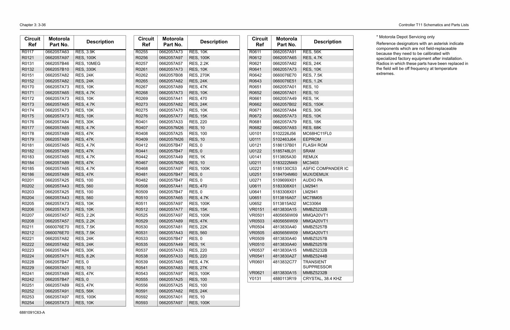
Chapter 3: 3-36 Controller T11 Schematics and Parts Lists
688109
* Motorola Depot Servicing onlyReference designators with an asterisk indicate components which are not field-replaceable because they need to be calibrated with specialized factory equipment after installation. Radios in which these parts have been replaced in the field will be off frequency at temperature extremes.
R0117R012R013R013R015R015R017R017R017R017R017R017R017R017R017R017R018R018R018R018R018R018R020R020R020R020R020R020R020R020R0211R021R022R022R022R022R022R022R024R024R025R025R025R025
CircR
, 56K, 4.7K, 24K, 10K, 7.5K, 1.2K, 10, 10, 1K, 150K, 30K, 10K, 18K, 68K8HC11FL0ROMSH ROMMUX403IC COMPANDER IC/DEMUXIO PA9419418M053064Z5232BA20VT1A20VT1Z5257BA20VT1Z5257BZ5257BZ5232BZ5244B
NSIENT PRESSORZ5232BSTAL, 38.4 KHZ
Description
1C63-A
0662057A63 RES, 3.9K1 0662057A97 RES, 100K1 0662057B46 RES, 10MEG2 0662057B10 RES, 330K1 0662057A82 RES, 24K2 0662057A82 RES, 24K0 0662057A73 RES, 10K1 0662057A65 RES, 4.7K2 0662057A73 RES, 10K3 0662057A65 RES, 4.7K4 0662057A73 RES, 10K5 0662057A73 RES, 10K6 0662057A84 RES, 30K7 0662057A65 RES, 4.7K8 0662057A89 RES, 47K9 0662057A89 RES, 47K1 0662057A65 RES, 4.7K2 0662057A89 RES, 47K3 0662057A65 RES, 4.7K4 0662057A89 RES, 47K5 0662057A65 RES, 4.7K6 0662057A89 RES, 47K1 0662057A25 RES, 1002 0662057A43 RES, 5603 0662057A25 RES, 1004 0662057A43 RES, 5605 0662057A73 RES, 10K6 0662057A73 RES, 10K7 0662057A57 RES, 2.2K8 0662057A57 RES, 2.2K
0660076E70 RES, 7.5K2 0660076E70 RES, 7.5K1 0662057A82 RES, 24K2 0662057A82 RES, 24K3 0662057A84 RES, 30K4 0662057A71 RES, 8.2K8 0662057B47 RES, 09 0662057A01 RES, 101 0662057A89 RES, 47K2 0662057B47 RES, 01 0662057A89 RES, 47K2 0662057A91 RES, 56K3 0662057A97 RES, 100K4 0662057A73 RES, 10K
uit ef
Motorola Part No. Description
R0255 0662057A73 RES, 10KR0256 0662057A97 RES, 100KR0257 0662057A57 RES, 2.2KR0261 0662057A73 RES, 10KR0262 0662057B08 RES, 270KR0265 0662057A82 RES, 24KR0267 0662057A89 RES, 47KR0268 0662057A73 RES, 10KR0269 0662057A41 RES, 470R0273 0662057A82 RES, 24KR0275 0662057A73 RES, 10KR0276 0662057A77 RES, 15KR0401 0662057A33 RES, 220R0407 0662057M26 RES, 10R0408 0662057A25 RES, 100R0409 0662057M26 RES, 10R0412 0662057B47 RES, 0R0441 0662057B47 RES, 0R0442 0662057A49 RES, 1KR0467 0662057M26 RES, 10R0468 0662057A97 RES, 100KR0481 0662057B47 RES, 0R0482 0662057B47 RES, 0R0508 0662057A41 RES, 470R0509 0662057B47 RES, 0R0510 0662057A65 RES, 4.7KR0511 0662057A97 RES, 100KR0512 0662057A77 RES, 15KR0525 0662057A97 RES, 100KR0529 0662057A89 RES, 47KR0530 0662057A81 RES, 22KR0531 0662057A43 RES, 560R0533 0662057B47 RES, 0R0535 0662057A49 RES, 1KR0537 0662057A33 RES, 220R0538 0662057A33 RES, 220R0539 0662057A65 RES, 4.7KR0541 0662057A83 RES, 27KR0543 0662057A97 RES, 100KR0555 0662057A25 RES, 100R0556 0662057A25 RES, 100R0591 0662057A82 RES, 24KR0592 0662057A01 RES, 10R0593 0662057A97 RES, 100K
Circuit Ref
Motorola Part No. Description
R0611 0662057A91 RESR0612 0662057A65 RESR0621 0662057A82 RESR0641 0662057A73 RESR0642 0660076E70 RESR0643 0660076E51 RESR0651 0662057A01 RESR0652 0662057A01 RESR0661 0662057A49 RESR0662 0662057B02 RESR0671 0662057A84 RESR0672 0662057A73 RESR0681 0662057A79 RESR0682 0662057A93 RESU0101 5102226J56 MC6U0111 5102463J64 EEPU0121 5186137B01 FLAU0122 5185748L01 SRAU0141 5113805A30 REMU0211 5183222M49 MC3U0221 5185130C53 ASFU0251 5184704M60 MUXU0271 5109699X01 AUDU0611 5183308X01 LM2U0641 5183308X01 LM2U0651 5113816A07 MC7U0652 5113815A02 MC3VR0151 4813830A15 MMBVR0501 4805656W09 MMQVR0503 4805656W09 MMQVR0504 4813830A40 MMBVR0505 4805656W09 MMQVR0509 4813830A40 MMBVR0510 4813830A40 MMBVR0537 4813830A15 MMBVR0541 4813830A27 MMBVR0601 4813832C77 TRA
SUPVR0621 4813830A15 MMBY0131 4880113R19 CRY
Circuit Ref
Motorola Part No.
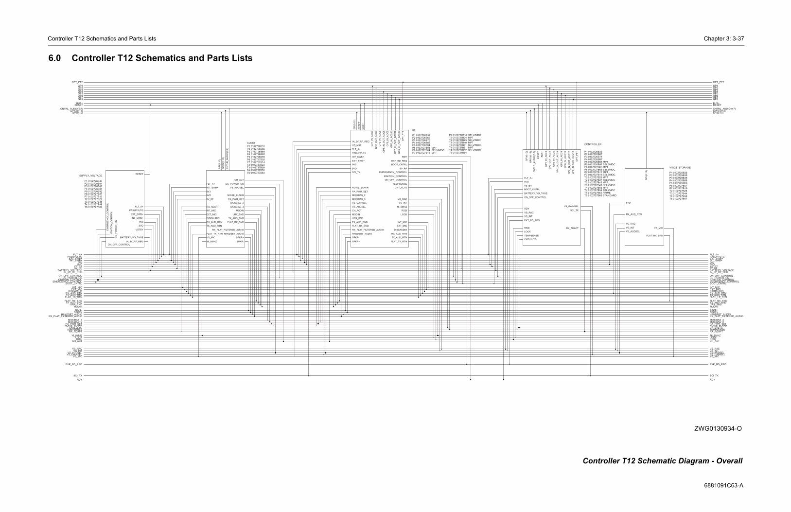
Controller T12 Schematics and Parts Lists Chapter 3: 3-37
6881091C63-A
6
T4 0102727B54 SEL5/MDCT4 0102727B53 MPT
P6 0102727B05 MPT
P4 0102726B87
P1 0102726B35
T6 0102727B66 STANDARDT6 0102727B65 PRIME
P6 0102727B06 SEL5/MDC
P5 0102726B97 SEL5/MDC
P5 0102726B96
P5 0102726B95 MPT
T2 0102727B26 MPT
T2 0102727B28P7 0102727B19
T3 0102727B43 SEL5/MDC
P7 0102727B17 MPTP7 0102727B18 SEL5/MDC
P6 0102727B07
P3 0102726B35P2 0102726B35
P4 0102726B88T2 0102727B27 SEL5/MDCT3 0102727B42 MPT
T3 0102727B44T4 0102727B55
P2 0102726B67P3 0102726B71
T6 0102727B67
P1 0102726B33
VSTBY
VS_GAINSEL
VS_INT
VS_RAC
VOICE_STORAGE
5VD
FLAT_RX_SND
RX_AUD_RTN
SP
I(0
:10
)
VS_AUDSEL
VS_INT VS_MIC
VS_RAC
GP
4_IN
_O
UT
_A
CC
8
GP
5_
IN_
AC
C9
GP
6_IN
_A
CC
10
GP
7_IN
_O
UT
_A
CC
12
GP
8_IN
_O
UT
_A
CC
14
GP
IO(0
:13)
LOCK
ON_OFF_CONTROL
OP
T_P
TT
RDY
RE
SE
T
RSSI RX_ADAPT
SCI_TX
SP
I(0:1
0)
TEMPSENSE
CONTROLLER
5VD
BATTERY_VOLTAGE
BOOT_CNTRL
BU
S+
CN
TL
R_
AU
DIO
(0:7
)
CNTLVLTG
EXT_BD_REQ
FLT_A+
GP
1_
IN_
AC
C3
GP
2_O
UT
_A
CC
4
GP
3_
IN_
AC
C6
PASUPVLTGFLT_A+
RX_ADAPT
CH_ACT
URX_SND
VS_GAINSEL
MOSBIAS_3
INT_SWB+
EXT_MIC
IN_5V_RF_REG
SCI_TX
VS_MIC
5VD9V3
EXT_SWB+
SPKR+SPKR-
EMERGENCY_CONTROLIGNITION_CONTROLDC_POWER_ONON_OFF_CONTROL
BATTERY_VOLTAGE
VSTBY
RDY
OPT_PTT
MODIN
TX_AUD_SNDFLAT_RX_SND
16_8MHZ
TX_AUD_RTNFLAT_TX_RTN
RX_AUD_RTNDISCAUDIO
INT_MIC
5V_RF
RX_FLAT_FILTERED_AUDIORHANDSET_AUDIO
GP1
EXP_BD_REQ
BOOT_CNTRL
VS_AUDSEL
TEMPSENSECNTLVLTG
VS_RACVS_INT
RSSILOCK
NOISE_BLNKRPA_PWR_SETMOSBIAS_2
CNTRL_AUDIO(0:7)GPIO(0:13)SPI(0:10)
BUS+RESET
GP8GP7GP6GP5GP4GP3GP2
ZWG0130934-O
Controller T12 Schematic Diagram - Overall
.0 Controller T12 Schematics and Parts Lists
T4 0102727B51 MPTT4 0102727B52 SELV/MDC
T4 0102727B50
P1 0102726B31
P2 0102726B64
T6 0102727B64
P6 0102727B01
P3 0102726B68
P2 0102726B65
P1 0102726B30
T6 0102727B63
P5 0102726B94
P5 0102726B93
- - - - -
T3 0102727B41 SELV/MDCP4 0102726B86
P4 0102726B85
P7 0102727B14
P4 0102726B84
T2 0102727B22
P6 0102727B02
P5 0102726B92
T2 0102727B25 SELV/MDC
T2 0102727B23
T2 0102727B24 MPT
T3 0102727B38
T6 0102727B62
X X- - -
T4 0102727B49
P7 0102727B16 SELV/MDC
P7 0102727B15 MPT
X
X
X X
P2 0102726B66P3 0102726B70
P3 0102726B69
X
X X
X
X
X X
X
- -
-
---
-
SPKR-
TX_AUD_RTN
TX_AUD_SND
URX_SND
VS_AUDSEL
VS_MIC
T3 0102727B39
T3 0102727B40 MPT
P7 0102727B13
P6 0102727B04 SELV/MDCP6 0102727B03 MPT
P1 0102726B32
Suppl.Vltg.
Audio
I/O
CNTLR
Voice Stor.
T4 T5 T6 T7 T8 T9
Controller Module Vesions Changes
X
FLAT_TX_RTN
FLT_A+
GP
IO(0
:13)
HANDSET_AUDIO
INT_MIC
INT_SWB+
MODIN
MOSBIAS_2
MOSBIAS_3
NOISE_BLNKR
PA_PWR_SET
RX_ADAPT
RX_AUD_RTN
RX_FLAT_FILTERED_AUDIO
SP
I(0:1
0)
SPKR+
VS_AUDSEL
VS_GAINSEL VS_INT
VS_MIC
VS_RAC
AUDIO
16_8MHZ
5VD
5V_RF
9V3
CH_ACT
CN
TL
R_
AU
DIO
(0:7
)
DC_POWER_ON
DISCAUDIO
EXT_MIC
FLAT_RX_SND
OP
T_P
TT
PASUPVLTG
PA_PWR_SET
RDY
RE
SE
T
RSSI
RX_AUD_RTN
RX_FLAT_FILTERED_AUDIO
SCI_TX
SP
I(0:1
0)
SPKR+
SPKR-
TEMPSENSE
TX_AUD_RTN
TX_AUD_SND
URX_SND
GP
4_IN
_O
UT
_A
CC
8
GP
5_
IN_
AC
C9
GP
6_IN
_A
CC
10
GP
7_IN
_O
UT
_A
CC
12
GP
8_IN
_O
UT
_A
CC
14
HANDSET_AUDIO
IGNITION_CONTROL
INT_MIC
INT_SWB+
IN_5V_RF_REG
LOCKMODIN
MOSBIAS_2
MOSBIAS_3
NOISE_BLNKR
ON_OFF_CONTROL
9V3 BOOT_CNTRL
BU
S+
CH_ACT
CNTLVLTG
DISCAUDIO
EMERGENCY_CONTROL
EXP_BD_REQ
EXT_MIC
EXT_SWB+
FLAT_RX_SND
FLAT_TX_RTN
FLT_A+
GP
1_
IN_
AC
C3
GP
2_O
UT
_A
CC
4
GP
3_
IN_
AC
C6 IO
16_8MHZ
5VD 5V_RF
IN_5V_RF_REG
ON_OFF_CONTROL
PASUPVLTG
RESET
VSTBY
PASUPVLTGFLT_A+
RX_ADAPT
SUPPLY_VOLTAGE
5VD
9V3
BATTERY_VOLTAGEDC
_P
OW
ER
_O
N
EM
ER
GE
NC
Y_C
ON
TR
OL
EXT_SWB+
FLT_A+
IGN
ITIO
N_C
ON
TR
OL
INT_SWB+
CH_ACT
URX_SND
VS_GAINSEL
MOSBIAS_3
INT_SWB+
EXT_MIC
IN_5V_RF_REG
SCI_TX
VS_MIC
5VD9V3
EXT_SWB+
SPKR+SPKR-
EMERGENCY_CONTROLIGNITION_CONTROL
DC_POWER_ONON_OFF_CONTROL
BATTERY_VOLTAGE
VSTBY
RDY
OPT_PTT
MODIN
TX_AUD_SNDFLAT_RX_SND
16_8MHZ
TX_AUD_RTNFLAT_TX_RTN
RX_AUD_RTNDISCAUDIO
INT_MIC
5V_RF
X_FLAT_FILTERED_AUDIOHANDSET_AUDIO
GP1
EXP_BD_REQ
BOOT_CNTRL
VS_AUDSEL
TEMPSENSECNTLVLTG
VS_RACVS_INT
RSSILOCK
NOISE_BLNKRPA_PWR_SET
MOSBIAS_2
CNTRL_AUDIO(0:7)GPIO(0:13)
SPI(0:10)
BUS+RESET
GP8GP7GP6GP5GP4GP3GP2
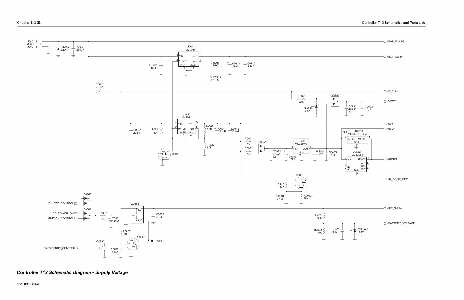
Chapter 3: 3-38 Controller T12 Schematics and Parts Lists
6881091
J0
VR06715.6VNU
Q0681
R068268K
1K
33uFC0652
R067130K
R067210K
C06710.1uF
J0
D0621
RESET1
VR06215.6V
GND
4
INPUT2
NC13
NC25
NC3 6NC4 7
8NC5
U0652MC330642
GND
1IN OUT
3MC78M05
U0651
C06550.1uF
C0621470pFNU
47uFC0622
R0621
24K
2INPUT
1RESET_
NUMC33464N-45ATR
U0653
3
GND
C065410uF
1F
J0
9V3
FLT_A+
IN_5V_RF_REG
RESET
5VD
BATTERY_VOLTAGE
EXT_SWB+
INT_SWB+
PASUPVLTG
VSTBY
Contro
C63-A
47K
47K
47K
47K
R0641
10K
601-1
.01uFC0662
150KR0662
Q0661
R061156K
R06818
57R01E0631
C0611
R0651
10
22uF
R06124.7K
D0661
Q0662
GND1
3
GND2
6
2 ON_OFF
VIN4VOUT 5
LM2941
U0611
ADJ1
601-3
Q0663
C0603
1K
10uF
R0661
TP0661
C06630.1uF
1.2KR0643
0.1uFC0651
C0645
NU
0.1uF
VR060124V
ADJ
GND1
3
GND2
6
ON_OFF2
4VIN
5VOUT
U0641LM2941
1
D0660
R0652
10Q0641
470pFC0601
C066147uF
R06427.5K
470pFC0641
33uFC0644
D0651
C0680.1u
601-2
0.1uFC0612
DC_POWER_ON
IGNITION_CONTROL
EMERGENCY_CONTROL
ON_OFF_CONTROL
ller T12 Schematic Diagram - Supply Voltage
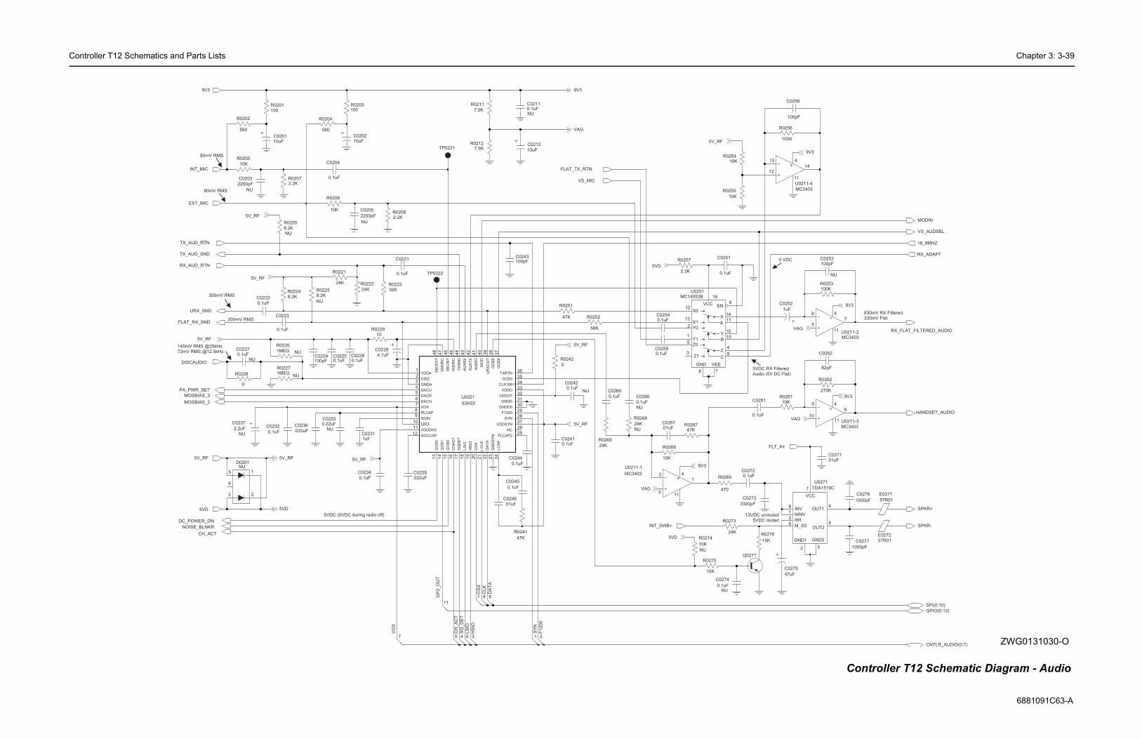
Controller T12 Schematics and Parts Lists Chapter 3: 3-39
6881091C63-A
ZWG0131030-O
U0211-2
6
5
7
4
11
MC3403
3300pF
C0273
0.1uFNU
C0274
10K
NU
R0274
MC3403
U0211-3
9
10
8
4
11
NU
C0253100pF
C0252
1uF
R0275
10K
Q0271
R0253100K
E0272
57R01
OUT26
3 RR
VCC
7
E0271
57R01
TDA1519C
GND1
2 5
GND2
INV9
M_SS8
NINV1
OUT14
U0271
7
C0262
82pF
C0275
24K
47uF
R0273
R0276
15K
C02720.1uFR0269
470
C0261
0.1uF
C0251
0.1uF
C0271.01uF
R0256
100K
0
1
15Y
0
1
4Z
0
1
A11
10B
9C
6EN
8
GND
16
VCC
7
VEE
14X
25153B
R0261
10K
1000pF
C0277
13
1214
4
11
MC3403
U0211-4
R0262
270K
C0256
100pF
C0276
1000pF
10K
R0255
10KR0254
5V_RF
RX_ADAPT
9V3
9V3
MODIN
9V3
16_8MHZ
SPKR-
FLT_A+
SPKR+
9V3
VS_AUDSEL
SPI(0:10)
GPIO(0:13)
CNTLR_AUDIO(0:7)
VAG
VAG
HANDSET_AUDIO
RX_FLAT_FILTERED_AUDIO
13VDC unmuted5VDC muted
0 VDC
630mV RX Filtered330mV Flat
5VDC RX FilteredAudio (0V DC Flat)
Controller T12 Schematic Diagram - Audio
F1
20
0
HS
IO
LS
IO
CL
K
SQ
_D
ET
VO
X
CH
_A
CT
GP
2_
OU
T
CS
X
SY
N
DA
TA
4
R02127.5K
7.5K
7
R0211
C0212
10uF
NU1MEG
R0226
R0241
47K
.01uF
C0246
5
C0232
0.1uF
R022910
C0227
NU0.1uF
C0223
56K0.1uF
R0252
NU1MEGR0227
2
C0236
.033uF
560
R0204
2.2KR0207
MC3403
U0211-1
2
3
1
4
11
100
10K
R0201
8
R0205
10uFC0201
NU
C0266
0.1uF
24K
R0266
NU
0.1uFC0225
NU
2.2uF
C0237 R02647K
C0245
0.1uF
C02410.1uF
TP0221
R0257
2.2K
8.2K
NU
R0225R02248.2K
C0244
0.1uF
.022uF
1uFC0231
C0235
R0228
0
C02260.1uF
4
0.1uF
C0265
D0201
5
3
1
2
R0251
47K
NU
7
3
0.1uFC0255
11
12X
13X
2 Y
1Y
5Z
Z3
U0MC140
C0267.01uF
6
2.2KR0208
C0203
2200pF
C0204
0.1uF
NU
R0202
560
0.1uF
9
C0222
R0220
8.2K
39
UR
XO
UT
1VDDA
32VDDCP
33VDDD
11VDDDAC
45
VD
DR
C
27VDDSYN
7VOX
NU
8PLCAP
25PLCAP2
17
SQ
DE
T
9SQIN
28SYN
36TXRTN
44
TX
SN
D
10UIO
23
GN
DS
YN
19
HS
IO
LC
AP
24
18
LS
IO
48
MIC
EX
T
46
MIC
INT
40
MO
D
26NC
13
GC
B2
35GCB3
GC
B4
37
38
GC
B5
3GNDA
31GNDD
30GNDD0
47
GN
DR
C
6DACG
5DACR
DACU4
22
DA
TA
2DISC
29F1200
15
GC
B0
14
GC
B1
12AGCCAP
41
AU
DIO
AU
XR
X4
3
42
AU
XT
X
16
CH
AC
T
21
CL
K
34CLK168
20
CS
X
U0221
63A53
C0242
NU0.1uF
R0221
24K
C0224 4.7uF
C0228
100pF
10K
R0265
R026824K
C02540.1uF
C0234
0.1uF
R0206
10K
NU
2200pF
C0205
0.22uFC0233
NU
C0243100pF
R0242
0
10uFC0202
R0203100
24K
R0222
C0221
0.1uF
1
NU0.1uFC0211
R0223
30K
5V_RF5V_RF
TX_AUD_RTN
5V_RF
TX_AUD_SND
5V_RF
DISCAUDIO
5V_RF
FLAT_TX_RTN
TP0222
INT_SWB+
CH_ACT
VAG
9V3 9V3
VS_MIC
MOSBIAS_3
VAG
EXT_MIC
5V_RF
5V_RF
5VD5VD
5V_RF
RX_AUD_RTN
INT_MIC
URX_SND
FLAT_RX_SND
DC_POWER_ON
5VD
5VD
PA_PWR_SET
MOSBIAS_2
NOISE_BLNKR
5VDC (0VDC during radio off)
145mV RMS @25kHz72mV RMS @12.5kHz
200mV RMS
300mV RMS
80mV RMS
80mV RMS
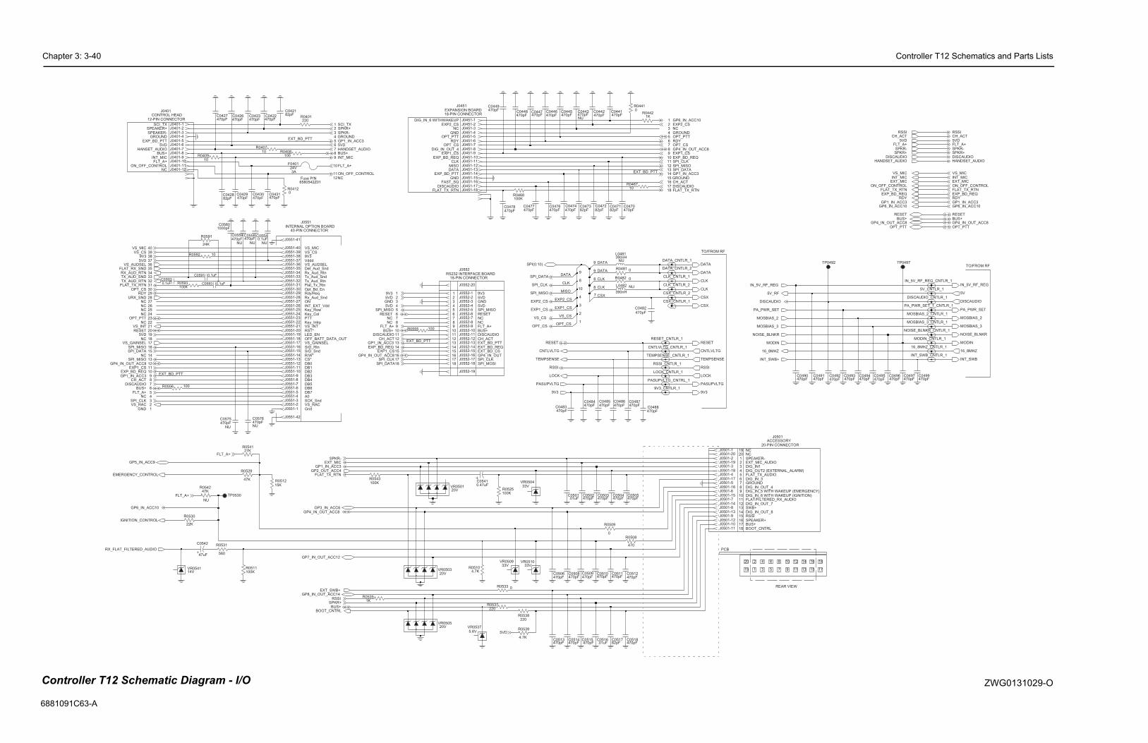
Chapter 3: 3-40 Controller T12 Schematics and Parts Lists
6881091
2
10
11
DIG_IN_OUT_4
15 17
6
GM300
SPEAKER-
1
PCB
NC
BOOT_CNTRL
20
13
J0501
3
1412
DIG_IN_6 WITH WAKEUP (IGNITION)
9
7
TO/FROM RF
34
DIG_IN1
NC
18
6
DIG_IN_OUT_7
2
DIG_OUT2 (EXTERNAL_ALARM)
8
8
5
ACCESSORY
DIG_IN_OUT_8SWB+
SPEAKER+BUS+
20-PIN CONNECTOR
20
REAR VIEW
15
16
FLAT/FILTERED_RX_AUDIO
RSSI
5
1213
1110
DIG_IN_5 WITH WAKEUP (EMERGENCY)
EXT_MIC_AUDIO1
17
GROUND
14
4
FLAT_TX_AUDIO
9
18
16
DIG_IN_3
19
WARIS
TO/FROM RF
19
7
J0501-4
J0501-14
PA_PWR_SET
16_8MHZ_CNTLR_1
PASUPVLTG
DISCAUDIO
J0501-16
MODIN
J0501-20
J0501-11
J0501-12
J0501-17
DATA
J0501-3
PA_PWR_SET_1_CNTLR_1
MOSBIAS_2_CNTLR_1
NOISE_BLNKR_CNTLR_1
J0501-5
470pFC0495
IN_5V_RF_REG
470pFC0497
J0501-8
RESET
5V_CNTLR_1
470pF
CSX
C0493
DISCAUDIO_CNTLR_1
MODIN_CNTLR_1
MOSBIAS_2
J0501-10
J0501-2
IN_5V_RF_REG_CNTLR_1
470pFC0491
TEMPSENSE
MOSBIAS_3
J0501-15
470pFC0499
J0501-6
TP0492
CLK
C0494470pF470pF
C0490
CLK
9V3
J0501-1
5V
DATA
J0501-13
INT_SWB_CNTLR_1
LOCK
J0501-9
CNTLVLTG
J0501-18
TP0497
INT_SWB
J0501-7
C0496470pF
16_8MHZ
CSX
J0501-19
NOISE_BLNKR
RSSI
MOSBIAS_3_CNTLR_1
C0492470pF
ACC8
GP6_IN_ACC10GP6_IN_ACC10
0
DISCAUDIO
MODIN
OPT_PTTOPT_PTT
INT_MIC INT_MIC
SPKR+SPKR+DISCAUDIO DISCAUDIO
HANDSET_AUDIOHANDSET_AUDIO
RSSI RSSI
IN_5V_RF_REG
GP1_IN_ACC3 GP1_IN_ACC3
INT_SWB+
EXP_BD_REQEXP_BD_REQ
CH_ACT CH_ACT
RDYRDY
NOISE_BLNKR
MOSBIAS_2
PA_PWR_SET
FLAT_TX_RTN FLAT_TX_RTN
GP4_IN_OUT_ACC8 GP4_IN_OUT_ACC8
MOSBIAS_3
VS_MIC VS_MIC
BUS+ BUS+RESETRESET
ON_OFF_CONTROL ON_OFF_CONTROL
16_8MHZ
5V_RF
5VD5VDFLT_A+FLT_A+
EXT_MICEXT_MIC
SPKR-SPKR-
Contr ZWG0131029-O
C63-A
35
22
GP4_IN_OUTSPI_CLK
9
Gnd
NC
1
9V3
VS_MIC
15
17
12
NC
BUS+
13
CLK
NC
23
GROUND
30
EXT_BD_REQEXT_BD_CS
21
SCK_Snd
NC
NC
7
EXP_BD_REQ
NC
NC
VS_GAINSEL
6580542Z01
CLK
Rdy/Req
EXT_BD_PTT
GROUND
Rx_Aud_Rtn
31
4
CS*
24
DISCAUDIO
7
Opt_Bd_En
6
11
2GND
5
151617
19
9
VS_CS
RDY
DATA
R/W*
16
GND
J0552
1
GROUND
CLK
4
11
GROUND
DB1
FLT_A+
Key_Col
SPI_MOSI
SPI_MISO
5VD
EXP2_CS
OFF_BATT_DATA_OUT
5VD9V3
5VD
DB2
3
EXP1_CS
Fuse P/N
6
1213
11
12
11
1
14
12
18-PIN CONNECTOR
17
4
1
7
9
18
121314
NC
10
OPT_CS
40
18-PIN CONNECTORRS232 INTERFACE BOARD
J0451
BUS+
6
1514
9
2
18
NC
DB5
EXP_BD_PTTGND
J0551
28
DATA
FAST_SQ
EXT_BD_PTT
GND4
DB6
16
DB3
5
NC
10
5
Key_Row
Key_Intrp
3
1516
NC
3
NC
23
7
17
NC
RESET
FLT_A+
DISCAUDIO
18
GND
INTERNAL OPTION BOARD
NC
Det_Aud_Snd
6
40-PIN CONNECTOR
29MISO
2
37
18
8
LED_EN
DATA
36
CONTROL HEADJ0401
EXT_BD_PTT
13
Flat_Tx_Rtn
MISO
1
SPEAKER-
1011
ON
VS_INT
2
A04NC
EXP_BD_PTT
SPEAKER+
14
HANSET_AUDIO
ON_OFF_CONTROL
EXT_BD_PTT
27
10
33
OPT_CS
SrD_Rtn
VS_RAC
8
RST*
7
34
5
3938
8
26
EXT_BD_PTT
12-PIN CONNECTOR
DB7
56
CLK
Tx_Aud_Rtn
PTT
EXP2_CS
CSX
10
8
EXPANSION BOARD
OPT_PTT
20
NC
INT_MIC
9
SrD_Snd
DB0
SCI_TX
Tx_Aud_Snd
Rx_Aud_Snd
VS_CS
DB4
3
32
Vddd
25
CH_ACT
DIG_IN_OUT_4
DATA
8 EXP1_CS
VS_AUDSEL
INT_EXT_Vdd
FLAT_TX_RTN
DIG_IN_6 WITHWAKEUP
J0551-41
J0451-1J0401-1
9
CNTLVLTG_CNTLR_1
470pFC0510
470pFC0487
R0525100K
J0401-11
470pFC0488
C0509
J0451-10
470pF
470pF
47K
NU
C0484
R0542
5.6VVR0537
J0551-25
220R0538
10
C0542
47uF
0R0533
220R0401
J0451-11
0
470
R0509
R0508
470pF
J0551-37
C0505
3A24V
F0401
J0551-8
C0426
.01uF
470pF
J0451-16
C0501
82pFC0421
20VVR0505
CLK_CNTLR_1
J0401-10
J0401-7
C0518470pF
NU
33VVR0509
470pFC0575
470pFC0423
R04120
J0552-19
J0552-18
R0555 100
100R0556
J0451-4
R0591
24K
J0551-23
J0551-18
NU470pFC0559
R0529
47K
470pF
8
C0513
J0552-9J0552-8
TEMPSENSE_CNTLR_1
J0401-9
J0551-3
J0551-10
C0477470pF
C0431470pF
10R0592
J0451-5
J0552-16J0552-17
470pFC0514
J0551-15
R0408100
C05601000pF
J0551-42
470pFC0442
VR050120V
J0551-4
J0551-14
470pFC0485
J0551-11
J0551-27
470pFC0429
J0551-32
J0551-36
82pFC0517
10R0407
R0531
560
RSSI_CNTLR_1
0R0441
2
C0541
CLK_CNTLR_2
0.47uF
J0551-40
NU
DATA_CNTLR_1
390nH
L0482
J0551-20
3
R0482 0
R0481 0
R0468100K
C0443470pFNU
J0451-17
7
J0451-6
1
100KR0543
R05104.7K
J0551-13
C0483470pF
R0511100K
CSX_CNTLR_1
J0401-5
J0552-3
470pFC0506
VR054114V
J0551-19
DATA_CNTLR_2
J0552-1
C0503470pF
82pFC0473
R0530
22K
4
J0401-3
TP0530
J0401-6
J0401-8
J0551-6
LOCK_CNTLR_1
C0591
470pF
0.1uF
C0471
C0422
82pF
470pF
J0551-22
C0447
C0508470pF
J0551-31
C047282pF
J0551-30
J0401-12
33VVR0510
9
J0451-12
C0449470pF
R051215K
C0486470pF
CSX_CNTLR_2
C05920.1uF
J0551-21
J0401-4
VR050320V
J0551-12
R0537220
J0451-18
8
J0451-15
J0451-7
10R0409
J0451-2
C0516.01uF
J0551-2
J0551-16
C0511470pF
C0512470pF
J0551-29
4.7K
R0539
J0551-39
J0551-28
J0451-9
C0430470pF
33V
100KR0593
VR0504
C0441470pF
J0552-5J0552-4
J0552-7J0552-6
J0551-33
C0482470pF
J0551-26
470pFNU
C0558
J0551-34
J0551-24
J0552-12
C0478470pF
470pFC0427
J0551-17
C0470470pF
R054127K
C0474470pF
390nHNU
L0481
C0504470pF
J0551-5
1KR0442
J0552-11J0552-10
470pFC0446 C0445470pF
0.1uFC0554
NU
J0451-3
J0451-8
R046710
J0551-9
C0593
J0552-15
0.1uF
J0552-2
J0551-7
C0476470pF
J0551-35
J0451-14
J0551-1
J0551-38
C042882pF
1KR0535
8
470pFC0448
J0451-13
470pF
RESET_CNTLR_1
C0515
PASUPVLTG_CNTRL_1
NU
J0401-2
C0576470pF
9
9V3_CNTLR_1
J0552-13J0552-14
470pFC0502
SPI_DATASPI_MISOSPI_CLK
EXP1_CSGP4_IN_OUT_OPT_CSRDYOPT_PTT
EXP2_CS
EXP_BD_REQ
5VD
SPKR-SPKR+
ON_OFF_CONTROL
BUS+
BUS+
GP6_IN_ACC10
J0552-20
SPKR-EXT_MIC
GP1_IN_ACC3GP2_OUT_ACC4
GP5_IN_ACC9
GP7_IN_OUT_ACC12
GP8_IN_OUT_ACC14
SPKR+
GP3_IN_ACC6GP4_IN_OUT_ACC8
EXP2_CS
FLAT_TX_RTN
FLAT_TX_RTN
GP6_IN_ACC1
GP1_IN_ACC3
FLT_A+
CH_ACT
GP1_IN_ACC3
9V3
SPI_MISO
CH_ACT
5VD9V3
5VDSPI_MISO
RESET
FLT_A+
DISCAUDIO
GP4_IN_OUT_ACC8EXP1_CS
EXP_BD_REQGP1_IN_ACC3
SPI_CLKSPI_DATA
OPT_PTT
INT_MIC
HANDSET_AUDIO
BOOT_CNTRL
5VD
BUS+
FLAT_TX_RTN
5VD
GP4_IN_OUT_ACC8EXP1_CS
EXP_BD_REQGP1_IN_ACC3
CH_ACTDISCAUDIO
FLT_A+
SCI_TX
RX_FLAT_FILTERED_AUDIO
EMERGENCY_CONTROL
RSSI
EXT_SWB+
RDY
EXP1_CS
9V3
DISCAUDIO
SPI(0:10)
FLT_A+
SPI_DATA
SPI_CLK
SPI_MISO
VS_CS
OPT_CS
RESET
RESET
PASUPVLTG
BUS+
TEMPSENSE
CNTLVLTG
RSSI
LOCK
OPT_CS
SPI_DATA
TX_AUD_RTN
VS_CSVS_MIC
SPI_CLK
FLAT_RX_SNDRX_AUD_RTN
URX_SND
TX_AUD_SND
VS_INT
5VDVS_AUDSEL
VS_GAINSELSPI_MISO
VS_RAC
IGNITION_CONTROL
FLT_A+
oller T12 Schematic Diagram - I/O

Controller T12 Schematics and Parts Lists Chapter 3: 3-41
6881091C63-A
GP7_OUT
T & DATA_PTT)
E_CS
HC138_A0
GP3_IN
GP8_IN
HC138_A2
GP2_OUT
GP4_IN
GP7_IN
HC138_A0EF_CS
XP2_CS
S_CS
XP1_CS
GP1_IN
GP5_IN
R0105 USED INSTANDARD ONLY
GP5_IN
GP7_IN
GP4_OUT
GP3_IN
GP8_IN
PE6VZIF_CS
GP6_IN
GP4_OUT
GP7_OUT
HC138_A2
GP6_IN
GP4_IN
GP8_OUT
HC138_A1
PT_CS
GP1_IN
GP8_OUT
HC138_A1
R0106 USED INPRIME ONLY
R0181
4.7K
0R0106
NU
Q0183
2
5
Q0171
Q0177
R018647K
30K
R0176
13
5
9
47K
R0182
R0105
100K
R017847K
2
R0171
4.7K
4.7K
R0183
8
D0179
2.2K
R0108
7
R0177
4.7K
83
13
0
4.7K
12
4
R0173
3
6
R018447K
10K
R0174
Q0185
47K
R0179
Q0173
1
7
NU100pF
C0106
Y411
Y510
Y69
Y77
12
0
EN_CS24
EN_CS35
GND
8
VCC
16
Y015
Y114
Y213
Y312
A0 1
A1 2
A2 3
EN_CS16
U0141
MC74HC138A
4.7KR0185
6
R0114
10K
Q0181
9
R0104
10K
11
R0170
10K
4
10
0.1uF
C0141
10K
R0172
10K
R0175
1
10
C01071000pF
CNTLVLTG
5VD
GP1_IN_ACC3
GP6_IN_ACC10
GP2_OUT_ACC4
5VD
IRQ
FROM_U0101_47
VS_RAC
5VD
VS_INT
GP4_IN_OUT_ACC8
5VD
GP3_IN_ACC6
5VD
RESET
RESET
5VD
GP5_IN_ACC9
GPIO(0:13)
GPIO(0:13)
FROM_U0101_46
5VD
5VD
FLT_A+
TEMPSENSE
VS_GAINSEL
EXT_BD_REQ
RSSI
5VD
5VD
LOCK
GP7_IN_OUT_ACC12
GP8_IN_OUT_ACC14
5VD
5VD
5VD
5VD
VSTBY
BATTERY_VOLTAGE
ZWG0130935-O
Controller T12 Schematic Diagram - Microprocessor
(EXT_BD_PT
E
SY
N
LS
IO
MICROPROCESSOR
DA
TA
MIS
O
F1200
VO
X
LS
IO
R
MIS
O
E
GP4_OUT
V
E
CLK
CS
X
GP7_OUT
CL
K
CH
AC
T
16Kx8bit
HS
IO
L
512kx8bit
RAM
DA
TA
EEPROM
HS
IO
ON_OFF_SENSE
O
32kx8bit
SQ
_D
ET
FLASH ROM
EE
_C
S
8
NU
C01080.1uF R0103
10
C0111
100pF
4.7K
R0102
NU
NU
C0103100pF
15
C0131
22pF
5.6VVR0151
14
9
7
2
TP0104
7
15
14
4
C0112
5
0.1uF
3
100K
R0121
0
10
0
6
13
4
4OUT
1IN
0
1
XTAL
Y0131
38.40KHz
2
NC
3
NC1
R0112
NU0
18
4
3
16
NU
R0110
10K
5
R0131
10MEG
4
NU
C0105100pF
D0101
4
R0117
3.9K
5
14
13
16
100pF
1
11
NU
C0123
R0113
10K
Q0151
8
VCC
2
GND
21IO0
IO122
IO223
IO325
IO426
IO527
IO628
IO729
A514
A6
A713
A83
A92
EN_CE30
EN_OE32
EN_WE7
24
11A15
A1610
A176
A189
A218
A317
A416
15
A020
A119
A1031
A111
A1212
4A13
A145
3
U0121
AT49F040
2
3
6
17
9
10K
5
7
R0101
TP0101
Q0110
47K
6
NU
R0107
9
1
4
1
17
7
10
9
C0122
0.1uF
3
2
TP0103
3
11 1
10
VSS
4
WP3
1
2
CS1
HOLD7
SCK6
SI5
SO2
VCC
8
12
U0111
X25128-2.7
R0151
24K
12
0
13
D0151
3
8
8
1
8
6
10
65
7
TP0151
0.1uFC0121
100pF
C0102
100pFC0104
NU
18
NU
C013222pF
0
7
4
C0151
.01uF
3
6
5
12
10
TP0102
6
8
2
12IO2
13IO3
15IO4
16IO5
17IO6
18IO7
19IO8
28
VCC
3A7
25A8
24A9
20EN_CS
22EN_OE
27EN_WE
GND
14
11IO1
2A12
26A13
1A14
8A2
7A3
6A4
A55
4A6
63A21U0122
10A0
9A1
A1021
23A11
11
69
VR
H
68
VR
L
13
VS
S
40
VS
SL
87
VS
SR
XF
C9
3
48XIRQ
91
XT
AL
76PJ5
77PJ6
78PJ7
94RESET
12
VD
D
39
VD
DL
88
VD
DR
92
VD
DS
YN
51
PI5
50
PI6
49
PI7
71PJ0_CSGP3
72PJ1_CSGP4
73PJ2
74PJ3
75PJ4
42PH5_CSGP1
41PH6_CSGP2
38PH7_CSPROG
56
PI0
55
PI1
54
PI2
53
PI3
52
PI4
18 PG5_XA185
PG6_AS
4PG7_R_W
47PH0_PW1
46PH1_PW2
45PH2_PW3
44PH3_PW4
43PH4_CSIO
23
PF
6_A
DD
R6
22
PF
7_A
DD
R7
29
PF
O_A
DD
R0
6PG0_XA13
16PG1_XA14
20PG2_XA15
19PG3_XA16
17PG4_XA17
PE5_AN562
PE6_AN661
PE7_AN760
28
PF
1_A
DD
R1
27
PF
2_A
DD
R2
26
PF
3_A
DD
R3
25
PF
4_A
DD
R4
24
PF
5_A
DD
R5
1P
D4_S
CK
2P
D5_S
S
PD
6_LV
IN3
PE0_AN067
PE1_AN166
PE2_AN265
PE3_AN364
PE4_AN463
34PC4_DATA4
35PC5_DATA5
36PC6_DATA6
37PC7_DATA7
97
PD
0_
RX
D
98
PD
1_T
XD
99
PD
2_M
ISO
100
PD
3_M
OS
I
15
PB
5_A
DD
R13
8P
B6_A
DD
R14
7P
B7_A
DD
R15
14
PB
O_A
DD
R8
30PC0_DATA0
31PC1_DATA1
32PC2_DATA2
33PC3_DATA3
83
PA
4_O
C4_O
C1
84
PA
5_O
C3_O
C1
85
PA
6_O
C2_O
C1
86
PA
7_P
A1_O
C1
10
PB
1_A
DD
R9
11
PB
2_A
DD
R10
9P
B3_A
DD
R11
21
PB
4_A
DD
R12
96IRQ
LV
OU
T9
5
58MODA_LIR
57MODB_VSTBY
79
PA
0_IC
3
80
PA
1_IC
2
81
PA
2_IC
1
82
PA
3_IC
4_O
C5_O
C1
59
AV
DD
70
AV
SS
89ECLK
90
EX
TA
L
U0101
MC68HC11FL0
5
0
NU
R0116
0
24K
R0152
330K
R0132
6
2
10K
7
R0115
R0111
0
9
C0101
100pF
RAM_CS
BUS+
SCI_TX
R_W
FLASH_CE
FLASH_OE
IRQ
ADDR_BUS(0:18)
DATA_BUS(0:7)
5VD
0
BOOT_CNTRL
ON_OFF_CONTROL
R_W
5VD
5VD
5VD
OPT_PTT
5VD
SPI(0:10)SPI(0:10) SPI(0:10) SPI(0:10) SPI(0:10)
CNTLR_AUDIO(0:7) CNTLR_AUDIO(0:7)CNTLR_AUDIO(0:7)CNTLR_AUDIO(0:7)
FROM_U0101_47
FROM_U0101_46
RAM_CS
5VD
RX_ADAPT
5VD5VD
FLT_A+ FLT_A+
FLASH_OE
NC
_X
TA
L
ECLK
NC
NC
RDY
ON_OFF_CONTROL
NC
FLASH_CE
R_W
5VD
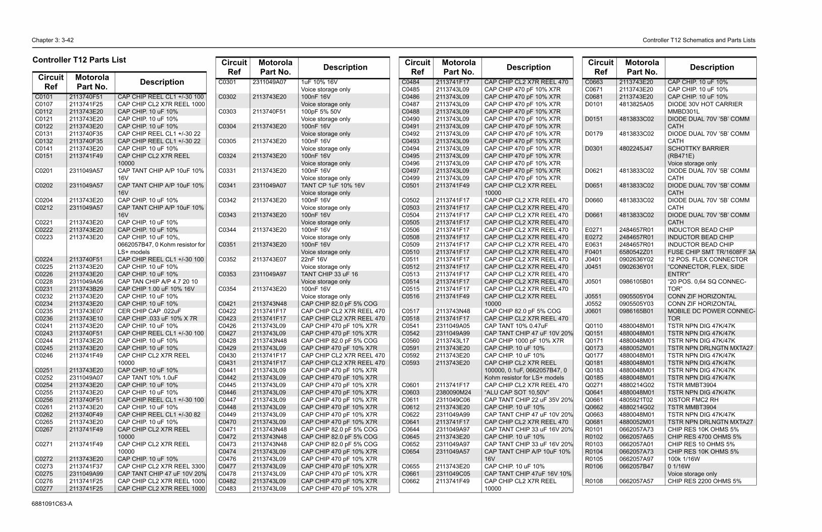
Chapter 3: 3-42 Controller T12 Schematics and Parts Lists
688109
Contr
CircRe
C0101C0107C0112C0121C0122C0131C0132C0141C0151
C0201
C0202
C0204C0212
C0221C0222C0223
C0224C0225C0226C0228C0231C0232C0234C0235C0236C0241C0243C0244C0245C0246
C0251C0252C0254C0255C0256C0261C0262C0265C0267
C0271
C0272C0273C0275C0276C0277
HIP CL2 X7R REEL 470HIP 470 pF 10% X7RHIP 470 pF 10% X7RHIP 470 pF 10% X7RHIP 470 pF 10% X7RHIP 470 pF 10% X7RHIP 470 pF 10% X7RHIP 470 pF 10% X7RHIP 470 pF 10% X7RHIP 470 pF 10% X7RHIP 470 pF 10% X7RHIP 470 pF 10% X7RHIP 470 pF 10% X7RHIP 470 pF 10% X7RHIP CL2 X7R REEL
HIP CL2 X7R REEL 470HIP CL2 X7R REEL 470HIP CL2 X7R REEL 470HIP CL2 X7R REEL 470HIP CL2 X7R REEL 470HIP CL2 X7R REEL 470HIP CL2 X7R REEL 470HIP CL2 X7R REEL 470HIP CL2 X7R REEL 470HIP CL2 X7R REEL 470HIP CL2 X7R REEL 470HIP CL2 X7R REEL 470HIP CL2 X7R REEL 470HIP CL2 X7R REEL
HIP 82.0 pF 5% COGHIP CL2 X7R REEL 470ANT 10% 0.47uFANT CHIP 47 uF 10V 20%HIP 1000 pF 10% X7RHIP. 10 uF 10%HIP. 10 uF 10%HIP CL2 X7R REEL
0, 0.1uF, 0662057B47, 0 resistor for LS+ modelsHIP CL2 X7R REEL 470AP SOT 10,50V”
ANT CHIP 22 uF 35V 20%HIP. 10 uF 10%ANT CHIP 47 uF 10V 20%HIP CL2 X7R REEL 470ANT CHIP 33 uF 16V 20%HIP. 10 uF 10%ANT CHIP 33 uF 16V 20%ANT CHIP A/P 10uF 10%
HIP. 10 uF 10%ANT CHIP 47uF 16V 10%HIP CL2 X7R REEL
DescriptionC0663 2113743E20 CAP CHIP. 10 uF 10%C0671 2113743E20 CAP CHIP. 10 uF 10%C0681 2113743E20 CAP CHIP. 10 uF 10%D0101 4813825A05 DIODE 30V HOT CARRIER
MMBD301LD0151 4813833C02 DIODE DUAL 70V ’5B’ COMM
CATHD0179 4813833C02 DIODE DUAL 70V ’5B’ COMM
CATHD0301 4802245J47 SCHOTTKY BARRIER
(RB471E) Voice storage only
D0621 4813833C02 DIODE DUAL 70V ’5B’ COMM CATH
D0651 4813833C02 DIODE DUAL 70V ’5B’ COMM CATH
D0660 4813833C02 DIODE DUAL 70V ’5B’ COMM CATH
D0661 4813833C02 DIODE DUAL 70V ’5B’ COMM CATH
E0271 2484657R01 INDUCTOR BEAD CHIPE0272 2484657R01 INDUCTOR BEAD CHIPE0631 2484657R01 INDUCTOR BEAD CHIPF0401 6580542Z01 FUSE CHIP SMT TR/1608FF 3AJ0401 0902636Y02 12 POS. FLEX CONNECTORJ0451 0902636Y01 “CONNECTOR, FLEX, SIDE
ENTRY”J0501 0986105B01 “20 POS. 0,64 SQ CONNEC-
TOR”J0551 0905505Y04 CONN ZIF HORIZONTALJ0552 0905505Y03 CONN ZIF HORIZONTALJ0601 0986165B01 MOBILE DC POWER CONNEC-
TORQ0110 4880048M01 TSTR NPN DIG 47K/47KQ0151 4880048M01 TSTR NPN DIG 47K/47KQ0171 4880048M01 TSTR NPN DIG 47K/47KQ0173 4880052M01 TSTR NPN DRLNGTN MXTA27Q0177 4880048M01 TSTR NPN DIG 47K/47KQ0181 4880048M01 TSTR NPN DIG 47K/47KQ0183 4880048M01 TSTR NPN DIG 47K/47KQ0185 4880048M01 TSTR NPN DIG 47K/47KQ0271 4880214G02 TSTR MMBT3904Q0641 4880048M01 TSTR NPN DIG 47K/47KQ0661 4805921T02 XISTOR FMC2 RHQ0662 4880214G02 TSTR MMBT3904Q0663 4880048M01 TSTR NPN DIG 47K/47KQ0681 4880052M01 TSTR NPN DRLNGTN MXTA27R0101 0662057A73 CHIP RES 10K OHMS 5%R0102 0662057A65 CHIP RES 4700 OHMS 5%R0103 0662057A01 CHIP RES 10 OHMS 5%R0104 0662057A73 CHIP RES 10K OHMS 5%R0105 0662057A97 100k 1/16WR0106 0662057B47 0 1/16W
Voice storage onlyR0108 0662057A57 CHIP RES 2200 OHMS 5%
Circuit Ref
Motorola Part No. Description
1C63-A
oller T12 Parts List
uit f
Motorola Part No. Description
2113740F51 CAP CHIP REEL CL1 +/-30 1002113741F25 CAP CHIP CL2 X7R REEL 10002113743E20 CAP CHIP. 10 uF 10%2113743E20 CAP CHIP. 10 uF 10%2113743E20 CAP CHIP. 10 uF 10%2113740F35 CAP CHIP REEL CL1 +/-30 222113740F35 CAP CHIP REEL CL1 +/-30 222113743E20 CAP CHIP. 10 uF 10%2113741F49 CAP CHIP CL2 X7R REEL
100002311049A57 CAP TANT CHIP A/P 10uF 10%
16V2311049A57 CAP TANT CHIP A/P 10uF 10%
16V2113743E20 CAP CHIP. 10 uF 10%2311049A57 CAP TANT CHIP A/P 10uF 10%
16V2113743E20 CAP CHIP. 10 uF 10%2113743E20 CAP CHIP. 10 uF 10%2113743E20 CAP CHIP. 10 uF 10%,
0662057B47, 0 Kohm resistor for LS+ models
2113740F51 CAP CHIP REEL CL1 +/-30 1002113743E20 CAP CHIP. 10 uF 10%2113743E20 CAP CHIP. 10 uF 10%2311049A56 CAP TAN CHIP A/P 4.7 20 102113743B29 CAP CHIP 1.00 uF 10% 16V2113743E20 CAP CHIP. 10 uF 10%2113743E20 CAP CHIP. 10 uF 10%2113743E07 CER CHIP CAP .022uF2113743E10 CAP CHIP .033 uF 10% X 7R2113743E20 CAP CHIP. 10 uF 10%2113740F51 CAP CHIP REEL CL1 +/-30 1002113743E20 CAP CHIP. 10 uF 10%2113743E20 CAP CHIP. 10 uF 10%2113741F49 CAP CHIP CL2 X7R REEL
100002113743E20 CAP CHIP. 10 uF 10%2311049A07 CAP TANT 10% 1.0uF2113743E20 CAP CHIP. 10 uF 10%2113743E20 CAP CHIP. 10 uF 10%2113740F51 CAP CHIP REEL CL1 +/-30 1002113743E20 CAP CHIP. 10 uF 10%2113740F49 CAP CHIP REEL CL1 +/-30 822113743E20 CAP CHIP. 10 uF 10%2113741F49 CAP CHIP CL2 X7R REEL
100002113741F49 CAP CHIP CL2 X7R REEL
100002113743E20 CAP CHIP. 10 uF 10%2113741F37 CAP CHIP CL2 X7R REEL 33002311049A99 CAP TANT CHIP 47 uF 10V 20%2113741F25 CAP CHIP CL2 X7R REEL 10002113741F25 CAP CHIP CL2 X7R REEL 1000
C0301 2311049A07 1uF 10% 16V Voice storage only
C0302 2113743E20 100nF 16VVoice storage only
C0303 2113740F51 100pF 5% 50VVoice storage only
C0304 2113743E20 100nF 16VVoice storage only
C0305 2113743E20 100nF 16VVoice storage only
C0324 2113743E20 100nF 16VVoice storage only
C0331 2113743E20 100nF 16VVoice storage only
C0341 2311049A07 TANT CP 1uF 10% 16VVoice storage only
C0342 2113743E20 100nF 16VVoice storage only
C0343 2113743E20 100nF 16VVoice storage only
C0344 2113743E20 100nF 16VVoice storage only
C0351 2113743E20 100nF 16VVoice storage only
C0352 2113743E07 22nF 16VVoice storage only
C0353 2311049A97 TANT CHIP 33 uF 16Voice storage only
C0354 2113743E20 100nF 16VVoice storage only
C0421 2113743N48 CAP CHIP 82.0 pF 5% COGC0422 2113741F17 CAP CHIP CL2 X7R REEL 470C0423 2113741F17 CAP CHIP CL2 X7R REEL 470C0426 2113743L09 CAP CHIP 470 pF 10% X7RC0427 2113743L09 CAP CHIP 470 pF 10% X7RC0428 2113743N48 CAP CHIP 82.0 pF 5% COGC0429 2113743L09 CAP CHIP 470 pF 10% X7RC0430 2113741F17 CAP CHIP CL2 X7R REEL 470C0431 2113741F17 CAP CHIP CL2 X7R REEL 470C0441 2113743L09 CAP CHIP 470 pF 10% X7RC0442 2113743L09 CAP CHIP 470 pF 10% X7RC0445 2113743L09 CAP CHIP 470 pF 10% X7RC0446 2113743L09 CAP CHIP 470 pF 10% X7RC0447 2113743L09 CAP CHIP 470 pF 10% X7RC0448 2113743L09 CAP CHIP 470 pF 10% X7RC0449 2113743L09 CAP CHIP 470 pF 10% X7RC0470 2113743L09 CAP CHIP 470 pF 10% X7RC0471 2113743N48 CAP CHIP 82.0 pF 5% COGC0472 2113743N48 CAP CHIP 82.0 pF 5% COGC0473 2113743N48 CAP CHIP 82.0 pF 5% COGC0474 2113743L09 CAP CHIP 470 pF 10% X7RC0476 2113743L09 CAP CHIP 470 pF 10% X7RC0477 2113743L09 CAP CHIP 470 pF 10% X7RC0478 2113743L09 CAP CHIP 470 pF 10% X7RC0482 2113743L09 CAP CHIP 470 pF 10% X7RC0483 2113743L09 CAP CHIP 470 pF 10% X7R
Circuit Ref
Motorola Part No. Description
C0484 2113741F17 CAP CC0485 2113743L09 CAP CC0486 2113743L09 CAP CC0487 2113743L09 CAP CC0488 2113743L09 CAP CC0490 2113743L09 CAP CC0491 2113743L09 CAP CC0492 2113743L09 CAP CC0493 2113743L09 CAP CC0494 2113743L09 CAP CC0495 2113743L09 CAP CC0496 2113743L09 CAP CC0497 2113743L09 CAP CC0499 2113743L09 CAP CC0501 2113741F49 CAP C
10000C0502 2113741F17 CAP CC0503 2113741F17 CAP CC0504 2113741F17 CAP CC0505 2113741F17 CAP CC0506 2113741F17 CAP CC0508 2113741F17 CAP CC0509 2113741F17 CAP CC0510 2113741F17 CAP CC0511 2113741F17 CAP CC0512 2113741F17 CAP CC0513 2113741F17 CAP CC0514 2113741F17 CAP CC0515 2113741F17 CAP CC0516 2113741F49 CAP C
10000C0517 2113743N48 CAP CC0518 2113741F17 CAP CC0541 2311049A05 CAP TC0542 2311049A99 CAP TC0560 2113743L17 CAP CC0591 2113743E20 CAP CC0592 2113743E20 CAP CC0593 2113743E20 CAP C
10000Kohm
C0601 2113741F17 CAP CC0603 2380090M24 “ALU CC0611 2311049C06 CAP TC0612 2113743E20 CAP CC0622 2311049A99 CAP TC0641 2113741F17 CAP CC0644 2311049A97 CAP TC0645 2113743E20 CAP CC0652 2311049A97 CAP TC0654 2311049A57 CAP T
16VC0655 2113743E20 CAP CC0661 2311049C05 CAP TC0662 2113741F49 CAP C
10000
Circuit Ref
Motorola Part No.
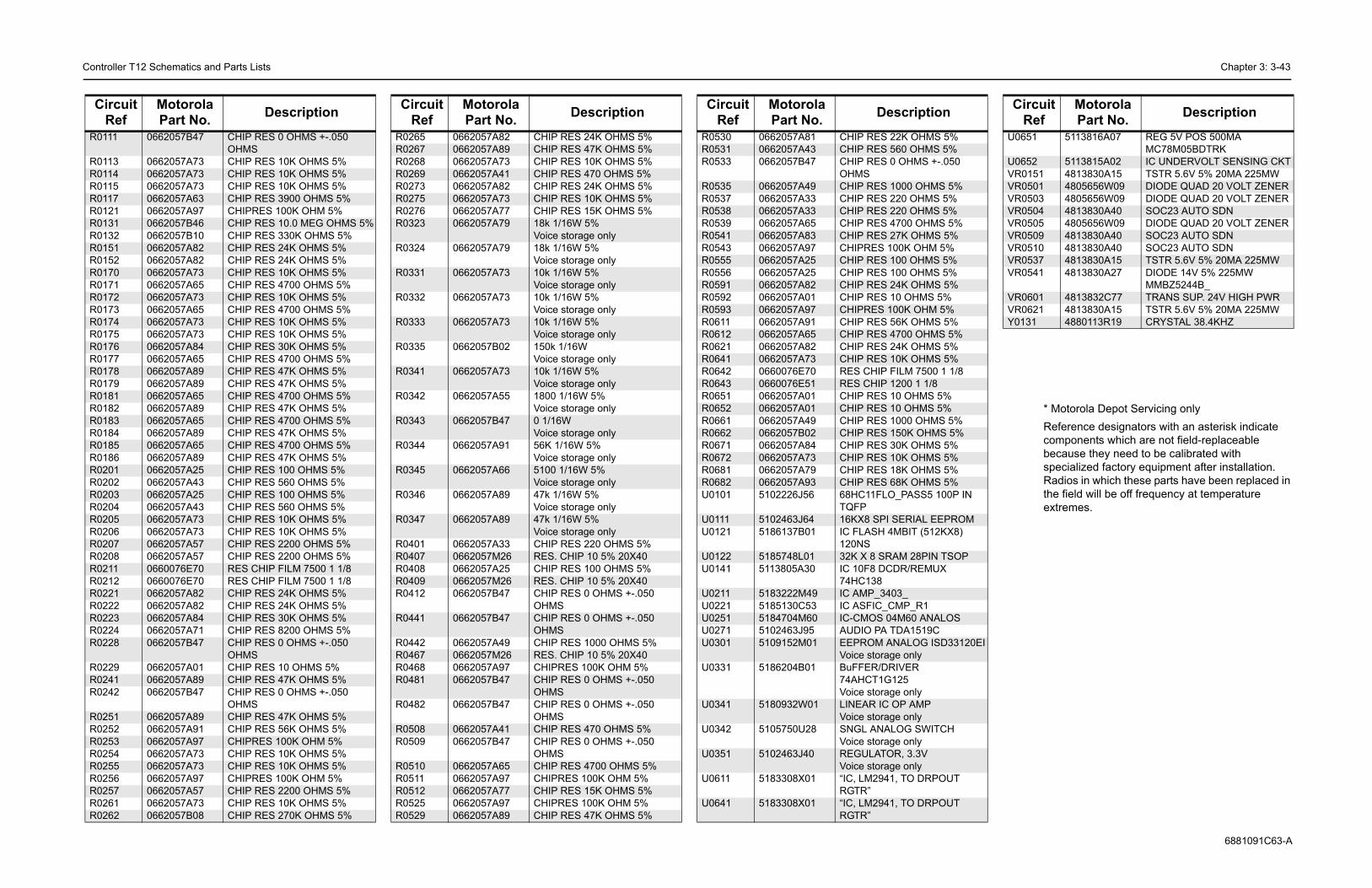
C Chapter 3: 3-43
6881091C63-A
* Motorola Depot Servicing onlyReference designators with an asterisk indicate components which are not field-replaceable because they need to be calibrated with specialized factory equipment after installation. Radios in which these parts have been replaced in the field will be off frequency at temperature extremes.
CHIP RES 22K OHMS 5%CHIP RES 560 OHMS 5%CHIP RES 0 OHMS +-.050 OHMSCHIP RES 1000 OHMS 5%CHIP RES 220 OHMS 5%CHIP RES 220 OHMS 5%CHIP RES 4700 OHMS 5%CHIP RES 27K OHMS 5%CHIPRES 100K OHM 5%CHIP RES 100 OHMS 5%CHIP RES 100 OHMS 5%CHIP RES 24K OHMS 5%CHIP RES 10 OHMS 5%CHIPRES 100K OHM 5%CHIP RES 56K OHMS 5%CHIP RES 4700 OHMS 5%CHIP RES 24K OHMS 5%CHIP RES 10K OHMS 5%RES CHIP FILM 7500 1 1/8RES CHIP 1200 1 1/8CHIP RES 10 OHMS 5%CHIP RES 10 OHMS 5%CHIP RES 1000 OHMS 5%CHIP RES 150K OHMS 5%CHIP RES 30K OHMS 5%CHIP RES 10K OHMS 5%CHIP RES 18K OHMS 5%CHIP RES 68K OHMS 5%68HC11FLO_PASS5 100P IN TQFP16KX8 SPI SERIAL EEPROMIC FLASH 4MBIT (512KX8) 120NS32K X 8 SRAM 28PIN TSOPIC 10F8 DCDR/REMUX 74HC138IC AMP_3403_IC ASFIC_CMP_R1IC-CMOS 04M60 ANALOSAUDIO PA TDA1519CEEPROM ANALOG ISD33120EIVoice storage onlyBuFFER/DRIVER 74AHCT1G125Voice storage onlyLINEAR IC OP AMPVoice storage onlySNGL ANALOG SWITCHVoice storage onlyREGULATOR, 3.3VVoice storage only“IC, LM2941, TO DRPOUT RGTR”“IC, LM2941, TO DRPOUT RGTR”
DescriptionU0651 5113816A07 REG 5V POS 500MA
MC78M05BDTRKU0652 5113815A02 IC UNDERVOLT SENSING CKTVR0151 4813830A15 TSTR 5.6V 5% 20MA 225MWVR0501 4805656W09 DIODE QUAD 20 VOLT ZENERVR0503 4805656W09 DIODE QUAD 20 VOLT ZENERVR0504 4813830A40 SOC23 AUTO SDNVR0505 4805656W09 DIODE QUAD 20 VOLT ZENERVR0509 4813830A40 SOC23 AUTO SDNVR0510 4813830A40 SOC23 AUTO SDNVR0537 4813830A15 TSTR 5.6V 5% 20MA 225MWVR0541 4813830A27 DIODE 14V 5% 225MW
MMBZ5244B_VR0601 4813832C77 TRANS SUP. 24V HIGH PWRVR0621 4813830A15 TSTR 5.6V 5% 20MA 225MWY0131 4880113R19 CRYSTAL 38.4KHZ
Circuit Ref
Motorola Part No. Description
ontroller T12 Schematics and Parts Lists
R0111 0662057B47 CHIP RES 0 OHMS +-.050 OHMS
R0113 0662057A73 CHIP RES 10K OHMS 5%R0114 0662057A73 CHIP RES 10K OHMS 5%R0115 0662057A73 CHIP RES 10K OHMS 5%R0117 0662057A63 CHIP RES 3900 OHMS 5%R0121 0662057A97 CHIPRES 100K OHM 5%R0131 0662057B46 CHIP RES 10.0 MEG OHMS 5%R0132 0662057B10 CHIP RES 330K OHMS 5%R0151 0662057A82 CHIP RES 24K OHMS 5%R0152 0662057A82 CHIP RES 24K OHMS 5%R0170 0662057A73 CHIP RES 10K OHMS 5%R0171 0662057A65 CHIP RES 4700 OHMS 5%R0172 0662057A73 CHIP RES 10K OHMS 5%R0173 0662057A65 CHIP RES 4700 OHMS 5%R0174 0662057A73 CHIP RES 10K OHMS 5%R0175 0662057A73 CHIP RES 10K OHMS 5%R0176 0662057A84 CHIP RES 30K OHMS 5%R0177 0662057A65 CHIP RES 4700 OHMS 5%R0178 0662057A89 CHIP RES 47K OHMS 5%R0179 0662057A89 CHIP RES 47K OHMS 5%R0181 0662057A65 CHIP RES 4700 OHMS 5%R0182 0662057A89 CHIP RES 47K OHMS 5%R0183 0662057A65 CHIP RES 4700 OHMS 5%R0184 0662057A89 CHIP RES 47K OHMS 5%R0185 0662057A65 CHIP RES 4700 OHMS 5%R0186 0662057A89 CHIP RES 47K OHMS 5%R0201 0662057A25 CHIP RES 100 OHMS 5%R0202 0662057A43 CHIP RES 560 OHMS 5%R0203 0662057A25 CHIP RES 100 OHMS 5%R0204 0662057A43 CHIP RES 560 OHMS 5%R0205 0662057A73 CHIP RES 10K OHMS 5%R0206 0662057A73 CHIP RES 10K OHMS 5%R0207 0662057A57 CHIP RES 2200 OHMS 5%R0208 0662057A57 CHIP RES 2200 OHMS 5%R0211 0660076E70 RES CHIP FILM 7500 1 1/8R0212 0660076E70 RES CHIP FILM 7500 1 1/8R0221 0662057A82 CHIP RES 24K OHMS 5%R0222 0662057A82 CHIP RES 24K OHMS 5%R0223 0662057A84 CHIP RES 30K OHMS 5%R0224 0662057A71 CHIP RES 8200 OHMS 5%R0228 0662057B47 CHIP RES 0 OHMS +-.050
OHMSR0229 0662057A01 CHIP RES 10 OHMS 5%R0241 0662057A89 CHIP RES 47K OHMS 5%R0242 0662057B47 CHIP RES 0 OHMS +-.050
OHMSR0251 0662057A89 CHIP RES 47K OHMS 5%R0252 0662057A91 CHIP RES 56K OHMS 5%R0253 0662057A97 CHIPRES 100K OHM 5%R0254 0662057A73 CHIP RES 10K OHMS 5%R0255 0662057A73 CHIP RES 10K OHMS 5%R0256 0662057A97 CHIPRES 100K OHM 5%R0257 0662057A57 CHIP RES 2200 OHMS 5%R0261 0662057A73 CHIP RES 10K OHMS 5%R0262 0662057B08 CHIP RES 270K OHMS 5%
Circuit Ref
Motorola Part No. Description
R0265 0662057A82 CHIP RES 24K OHMS 5%R0267 0662057A89 CHIP RES 47K OHMS 5%R0268 0662057A73 CHIP RES 10K OHMS 5%R0269 0662057A41 CHIP RES 470 OHMS 5%R0273 0662057A82 CHIP RES 24K OHMS 5%R0275 0662057A73 CHIP RES 10K OHMS 5%R0276 0662057A77 CHIP RES 15K OHMS 5%R0323 0662057A79 18k 1/16W 5%
Voice storage onlyR0324 0662057A79 18k 1/16W 5%
Voice storage onlyR0331 0662057A73 10k 1/16W 5%
Voice storage onlyR0332 0662057A73 10k 1/16W 5%
Voice storage onlyR0333 0662057A73 10k 1/16W 5%
Voice storage onlyR0335 0662057B02 150k 1/16W
Voice storage onlyR0341 0662057A73 10k 1/16W 5%
Voice storage onlyR0342 0662057A55 1800 1/16W 5%
Voice storage onlyR0343 0662057B47 0 1/16W
Voice storage onlyR0344 0662057A91 56K 1/16W 5%
Voice storage onlyR0345 0662057A66 5100 1/16W 5%
Voice storage onlyR0346 0662057A89 47k 1/16W 5%
Voice storage onlyR0347 0662057A89 47k 1/16W 5%
Voice storage onlyR0401 0662057A33 CHIP RES 220 OHMS 5%R0407 0662057M26 RES. CHIP 10 5% 20X40R0408 0662057A25 CHIP RES 100 OHMS 5%R0409 0662057M26 RES. CHIP 10 5% 20X40R0412 0662057B47 CHIP RES 0 OHMS +-.050
OHMSR0441 0662057B47 CHIP RES 0 OHMS +-.050
OHMSR0442 0662057A49 CHIP RES 1000 OHMS 5%R0467 0662057M26 RES. CHIP 10 5% 20X40R0468 0662057A97 CHIPRES 100K OHM 5%R0481 0662057B47 CHIP RES 0 OHMS +-.050
OHMSR0482 0662057B47 CHIP RES 0 OHMS +-.050
OHMSR0508 0662057A41 CHIP RES 470 OHMS 5%R0509 0662057B47 CHIP RES 0 OHMS +-.050
OHMSR0510 0662057A65 CHIP RES 4700 OHMS 5%R0511 0662057A97 CHIPRES 100K OHM 5%R0512 0662057A77 CHIP RES 15K OHMS 5%R0525 0662057A97 CHIPRES 100K OHM 5%R0529 0662057A89 CHIP RES 47K OHMS 5%
Circuit Ref
Motorola Part No. Description
R0530 0662057A81R0531 0662057A43R0533 0662057B47
R0535 0662057A49R0537 0662057A33R0538 0662057A33R0539 0662057A65R0541 0662057A83R0543 0662057A97R0555 0662057A25R0556 0662057A25R0591 0662057A82R0592 0662057A01R0593 0662057A97R0611 0662057A91R0612 0662057A65R0621 0662057A82R0641 0662057A73R0642 0660076E70R0643 0660076E51R0651 0662057A01R0652 0662057A01R0661 0662057A49R0662 0662057B02R0671 0662057A84R0672 0662057A73R0681 0662057A79R0682 0662057A93U0101 5102226J56
U0111 5102463J64U0121 5186137B01
U0122 5185748L01U0141 5113805A30
U0211 5183222M49U0221 5185130C53U0251 5184704M60U0271 5102463J95U0301 5109152M01
U0331 5186204B01
U0341 5180932W01
U0342 5105750U28
U0351 5102463J40
U0611 5183308X01
U0641 5183308X01
Circuit Ref
Motorola Part No.
Chapter 3: 3-44 Controller T12 Schematics and Parts Lists
6881091
Notes
C63-A

Chapter 4: i
Chapter 4: VHF (136-174 MHz) 1-25W Service InformationTable of Contents
Section 1 Model Charts and Technical Specifications
1.0 VHF (136-174 MHz) 1-25W Model Charts........................................................4:1-11.1 CDM Series Model Chart ............................................................................4:1-11.2 PRO Series Model Chart.............................................................................4:1-2
2.0 Technical Specifications ...................................................................................4:1-2
Section 2 Theory of Operation
1.0 Introduction .......................................................................................................4:2-12.0 VHF (136-174 MHz) 1-25W Receiver Front-End..............................................4:2-1
2.1 Receiver Front-End .....................................................................................4:2-12.2 Front-End Bandpass Filters and Pre-Amplifier............................................4:2-22.3 First Mixer and High Intermediate Frequency (IF).......................................4:2-22.4 Low Intermediate Frequency (IF) and Receiver Back-End .........................4:2-2
3.0 VHF (136-174 MHz) 1-25W Transmitter Power Amplifier (PA) 25W ................4:2-33.1 First Power Controlled Stage ......................................................................4:2-33.2 Power Controlled Driver Stage....................................................................4:2-43.3 Final Stage ..................................................................................................4:2-43.4 Directional Coupler......................................................................................4:2-43.5 Antenna Switch ...........................................................................................4:2-53.6 Harmonic Filter ............................................................................................4:2-53.7 Power Control..............................................................................................4:2-5
4.0 VHF (136-174 MHz) 1-25W Frequency Synthesis ...........................................4:2-54.1 Reference Oscillator....................................................................................4:2-64.2 Fractional-N Synthesizer .............................................................................4:2-64.3 Voltage Controlled Oscillator (VCO)............................................................4:2-74.4 Synthesizer Operation.................................................................................4:2-8
Section 3 Troubleshooting Charts
1.0 Troubleshooting Flow Chart for Receiver .........................................................4:3-12.0 Troubleshooting Flow Chart for 25W Transmitter.............................................4:3-33.0 Troubleshooting Flow Chart for Synthesizer.....................................................4:3-64.0 Troubleshooting Flow Chart for VCO................................................................4:3-7
6881091C63-A
Chapter 4: ii
Section 4 VHF (136-174 MHz) 1-25W PCBs, Schematics, andParts Lists
1.0 Allocation of Schematics and Circuit Boards ................................................... 4:4-11.1 Controller Circuits ....................................................................................... 4:4-1
2.0 VHF (136-174 MHz) 1-25W PCB 8486172B04, Schematics, and Parts Lists.................................................................................................................. 4:4-3
3.0 VHF (136-174 MHz) 1-25W PCB 8486172B06, Schematics, and Parts Lists................................................................................................................ 4:4-13
4.0 VHF (136-174 MHz) 1-25W PCB 8486172B07, Schematics, and Parts Lists................................................................................................................ 4:4-23
5.0 VHF (136-174 MHz) 1-25W PCB 8486172B08, Schematics, and Parts Lists................................................................................................................ 4:4-30
6881091C63-A

Chapter 4: 1-1
Section 1MODEL CHARTS AND TECHNICAL SPECIFICATIONS
1.0 VHF (136-174 MHz) 1-25W Model Charts
1.1 CDM Series Model Chart
CDM Series, VHF (136-174 MHz) 1-25WModel Description
AAM25KHC9AA1AN CDM750, 136-174 MHz, 1-25W, 12.5/20/25 kHzAAM25KHD9AA2AN CDM1250, 136-174 MHz, 1-25W, 12.5/20/25 kHz
AAM25KHF9AA5AN CDM1550, 136-174 MHz, 1-25W, 12.5/20/25 kHz
Item Description
X GCN6112 Control Head, CDM750X GCN6113 Control Head, CDM1250
X GCN6114 Control Head, CDM1550X X X IMUD6014 Tanapa, VHF 136-174 MHz, 1-25W, 12.5/20/25 kHzX X X IMUD6014_S Replacement Board, VHF 136-174 MHz, 1-25W, 12.5/20/25 kHzX X X HAD4006 Antenna, 136-144 MHz, 1/4 Wave Roof Mount (Mini U)X X X HAD4007 Antenna, 146-150.8 MHz, 1/4 Wave Roof Mount (Mini U)X X X HAD4008 Antenna, 150.8-162 MHz, 1/4 Wave Roof Mount (Mini U)X X X HAD4009 Antenna, 162-174 MHz, 1/4 Wave Roof Mount (Mini U)X X X HAD4014 Antenna, 146-172 MHz, 3dB Gain Roof Mount (Mini U)X 6881091C54 User Guide, CDM750
X 6881091C55 User Guide, CDM1250X 6881091C56 User Guide, CDM1550
6881091C63-A

Chapter 4: 1-2 Technical Specifications
1.2 PRO Series Model Chart
2.0 Technical SpecificationsData is specified for +25°C unless otherwise stated.
PRO Series, VHF (136-174 MHz) 1-25WModel Description
LAM25KHC9AA1AN PRO3100, 136-174 MHz, 1-25W, 12.5/20/25 kHz Ch SpLAM25KHD9AA2AN PRO5100, 136-174 MHz, 1-25W, 12.5/20/25 kHz Ch Sp
LAM25KHF9AA5AN PRO7100, 136-174 MHz, 1-25W, 12.5/20/25 kHz Ch Sp
Item Description
X GCN6112 Control Head, PRO3100X GCN6113 Control Head, PRO5100
X GCN6114 Control Head, PRO7100X X X IMUD6014 Tanapa, VHF 136-174 MHz, 1-25W, 12.5/20/25 kHzX X X IMUD6014_S Replacement Board, VHF 136-174 MHz, 1-25W, 12.5/20/25 kHzX X X HAD4006 Antenna, 136-144 MHz, 1/4 Wave Roof Mount (Mini U)X X X HAD4007 Antenna, 146-150.8 MHz, 1/4 Wave Roof Mount (Mini U)X X X HAD4008 Antenna, 150.8-162 MHz, 1/4 Wave Roof Mount (Mini U)X X X HAD4009 Antenna, 162-174 MHz, 1/4 Wave Roof Mount (Mini U)X X X HAD4014 Antenna, 146-172 MHz, 3dB Gain Roof Mount (Mini U)X 6881091C57 User Guide, PRO3100
X 6881091C58 User Guide, PRO5100X 6881091C59 User Guide, PRO7100
General SpecificationsChannel Capacity
CDM750/PRO3100CDM1250/PRO5100CDM1550/PRO7100
464128
Power Supply 13.2Vdc (10.8 - 15.6Vdc)Dimensions: H x W x D (in./mm)
CDM750/PRO3100CDM1250/PRO5100 andCDM1550/PRO7100
Depth excludes knobs
1 - 25W:2.2 in. x 6.93 in. x 6.97 in. (56 mm x 176 mm x 177 mm)
2.34 in. x 7.05 in. x 7.32 in. (59 mm x 179 mm x 186 mm)
Add 0.35 in. (9mm) for Volume KnobWeight (All CDM and PRO models) 3.15 lb. (1430 g)Sealing: Withstands rain testing per
MIL STD 810 C/D /E and IP54Shock and Vibration: Protection provided via impact
resistant housing exceeding MIL STD 810-C/D /EDust, Salt & Fog Protection provided via environment resistant housing exceeding
MIL STD 810 C/D /E
6881091C63-A

Technical Specifications Chapter 4: 1-3
*Availability subject to the laws and regulations of individual countries.
Transmitter VHF*Frequencies - Full Bandsplit VHF 136-174 MHzChannel Spacing 12.5/20/25 kHzFrequency Stability(-30°C to +60°C, +25° Ref.)
±2.0 ppm
Power 1-25W Modulation Limiting ±2.5 @ 12.5 kHz
±4.0 @ 20 kHz±5.0 @ 25 kHz
FM Hum & Noise -40 dB @ 12.5 kHz-45 dB @ 20/25 kHz
Conducted/Radiated Emission -36 dBm <1 GHz-30 dBm >1 GHz
Adjacent Channel Power -60 dB @ 12.5 kHz-70 dB @ 25 kHz
Audio Response(300 - 3000Hz @ 20/25 kHz)(300 - 2550Hz @12.5 kHz)
+1 to -3 dB TIA/EIA box
Audio Distortion@1000Hz, 60%Rated Maximum Deviation
<3% typical
Receiver VHF*Frequencies - Full Bandsplit VHF 136-174 MHzChannel Spacing 12.5/20/25 kHzSensitivity (12 dB SINAD) 0.30 µV (0.22 µV typical)Intermodulation >65 dB (ETS)
75 dB @ 12.5 kHz (TIA)78 dB @ 25 kHz (TIA)Base Mode: >70dB (1-25W model only)
Adjacent Channel Selectivity 65 dB @ 12.5 kHz 75 dB @ 20 kHz80 dB @ 25 kHz
Spurious Rejection 75 dB @ 12.5 kHz80 dB @ 20/25 kHz
Rated Audio 3W Internal7.5W External13W External
Audio Distortion @ Rated Audio <3% typicalHum & Noise -40 dB @ 12.5 kHz
-45 dB @ 20/25 kHzAudio Response(300 - 3000Hz @ 20/25 kHz)(300 - 2550Hz @12.5 kHz)
+1 to -3 dB TIA/EIA box
Conducted Spurious Emission -57 dBm <1 GHz-47 dBm >1 GHz
6881091C63-A
Chapter 4: 1-4 Technical Specifications
Notes
6881091C63-A

Chapter 4: 2-1
Section 2THEORY OF OPERATION
1.0 IntroductionThis chapter provides a detailed theory of operation for the VHF circuits in the radio. For details of the theory of operation and troubleshooting for the associated controller circuits refer to the controller section of this manual.
2.0 VHF (136-174 MHz) 1-25W Receiver Front-End2.1 Receiver Front-End
The receiver is able to cover the VHF range from 136 to 174 MHz. It consists of four major blocks: front-end bandpass filters and pre-amplifier, first mixer, high-IF, low-IF and receiver back-end. Two varactor-tuned bandpass filters perform antenna signal pre-selection. A passive double-balanced mixer converts the signal to the first IF of 44.85 MHz. High-side first injection is used.
Figure 4-1 VHF Receiver Block Diagram
Demodulator
1. Crystal Filter
MixerVaractor Tuned FilterRF AmpVaractor
Tuned Filter
Antenna
Control Voltagefrom PCIC First LO
from FGU
Recovered Audio
RSSI
IF
Second LO
2. Crystal Filter
455kHz Filter(25kHz)
455kHz Filter(25kHz)
455kHz Filter(12.5kHz)
455kHz Filter(12.5kHz)
Switc
h
Switc
h
Switc
h
Switc
h
Limiter
1. IF Amp
2. IF Amp
Filter Bank Selectionfrom Synthesizer IC
Pin Diode Antenna SwitchRF Jack
Harmonic Filter
6881091C63-A
Chapter 4: 2-2 VHF (136-174 MHz) 1-25W Receiver Front-End
There are two 2-pole 44.85 MHz crystal filters in the high-IF section and 2 pairs of 455 kHz ceramic filters in the low-IF section to provide the required adjacent channel selectivity. The correct pair of ceramic filters for 12.5 or 25kHz channel spacing is selected via control line BWSELECT. The second IF at 455 kHz is mixed, amplified and demodulated in the IF IC. The processing of the demodulated audio signal is performed by an audio processing IC located in the controller section.
2.2 Front-End Bandpass Filters and Pre-Amplifier
The received signal from the radio’s antenna connector is first routed through the harmonic filter and antenna switch, which are part of the RF power amplifier circuitry, before being applied to the receiver pre-selector filter (C3001, C3002, D3001 and associated components). The 2-pole pre-selector filter tuned by the dual varactor diode D3001 pre-selects the incoming signal (RXIN) from the antenna switch to reduce spurious effects to following stages. The tuning voltage (FECNTL_1) ranging from 2 volts to 8 volts is controlled by pin 20 of PCIC (U3501) in the Transmitter section. A dual hot carrier diode (D3003) limits any inband signal to 0 dBm to prevent damage to the pre-amplifier.
The RF pre-amplifier is an SMD device (Q3001) with collector-base feedback to stabilize gain, impedance, and intermodulation. Transistor Q3002 compares the voltage drop across resistor R3002 with a fixed base voltage from divider R3011, R3000 and R3012, and adjusts the base current of Q3001 as necessary to maintain its collector current constant at approximately 15-20 mA. Operating voltage is from the regulated 9.3V supply (9V3). During transmit, 9.1 volts (K9V1) turns off both transistors Q3002 and Q3001. This protects the RF pre-amplifier from excessive dissipation during transmit mode. A switchable 3dB pad (R3022, R3024, R3016 and R3018) controlled via Line FECNTL_2 and Q3021 stabilizes the output impedance and intermodulation performance.
A second 2-pole varactor tuned bandpass filter provides additional filtering of the amplified signal. The dual varactor diode D3004 is controlled by the same signal FECNTL_1, which controls the pre-selector filter.
2.3 First Mixer and High Intermediate Frequency (IF)
The signal coming from the front-end is converted to the high-IF frequency of 44.85 MHz using a passive double-balanced mixer (D3031). Its ports are matched for incoming RF signal conversion to the 44.85 MHz IF using high side injection. The high-side injection signal (RXINJ) from the frequency synthesizer circuitry has a level of approximately 13 dBm and is injected via matching transformer T3002.
The mixer IF output signal (IF) from transformer T3001 pin 2 is fed to the first two pole crystal filter FL3101. The filter output in turn is matched to the following IF amplifier.
The IF amplifier Q3101 is actively biased by a collector base feedback (R3101, R3106) to a current drain of approximately 5 mA drawn from the voltage 5V. Its output impedance is matched to the second two pole crystal filter FL3102. The signal is further amplified by a pre-amplifier (Q3102) before going into pin 1 of IFIC (U3101).
A dual hot carrier diode (D3101) limits the filter output voltage swing to reduce overdrive effects at RF input levels above -27 dBm.
2.4 Low Intermediate Frequency (IF) and Receiver Back-End
The 44.85 MHz high-IF signal from the second IF amplifier feeds the IF IC (U3101) at pin 1. Within the IF IC, the 44.85 MHz high IF signal mixes with the 44.395 MHz second local oscillator (2nd LO) to produce the low-IF signal at 455 kHz. The 2nd LO frequency is determined by crystal Y3101. The low IF signal is amplified and filtered by an external pair of 455 kHz ceramic filters FL3112, FL3114
6881091C63-A
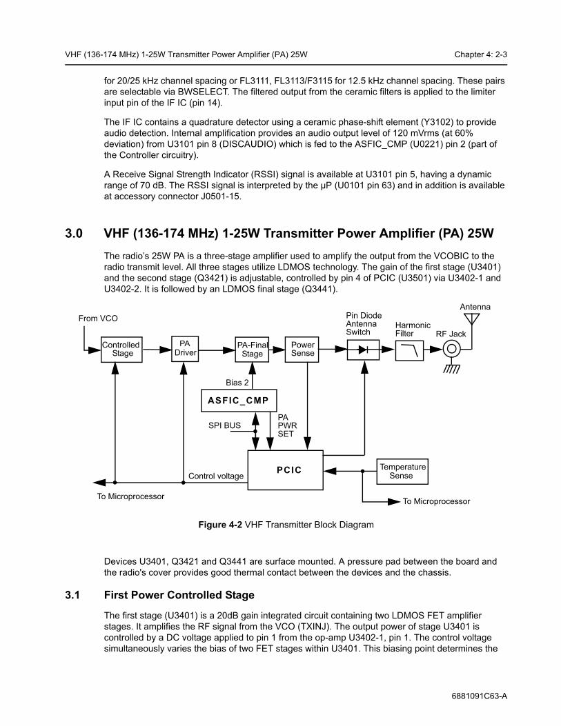
VHF (136-174 MHz) 1-25W Transmitter Power Amplifier (PA) 25W Chapter 4: 2-3
for 20/25 kHz channel spacing or FL3111, FL3113/F3115 for 12.5 kHz channel spacing. These pairs are selectable via BWSELECT. The filtered output from the ceramic filters is applied to the limiter input pin of the IF IC (pin 14).
The IF IC contains a quadrature detector using a ceramic phase-shift element (Y3102) to provide audio detection. Internal amplification provides an audio output level of 120 mVrms (at 60% deviation) from U3101 pin 8 (DISCAUDIO) which is fed to the ASFIC_CMP (U0221) pin 2 (part of the Controller circuitry).
A Receive Signal Strength Indicator (RSSI) signal is available at U3101 pin 5, having a dynamic range of 70 dB. The RSSI signal is interpreted by the µP (U0101 pin 63) and in addition is available at accessory connector J0501-15.
3.0 VHF (136-174 MHz) 1-25W Transmitter Power Amplifier (PA) 25WThe radio’s 25W PA is a three-stage amplifier used to amplify the output from the VCOBIC to the radio transmit level. All three stages utilize LDMOS technology. The gain of the first stage (U3401) and the second stage (Q3421) is adjustable, controlled by pin 4 of PCIC (U3501) via U3402-1 and U3402-2. It is followed by an LDMOS final stage (Q3441).
Figure 4-2 VHF Transmitter Block Diagram
Devices U3401, Q3421 and Q3441 are surface mounted. A pressure pad between the board and the radio's cover provides good thermal contact between the devices and the chassis.
3.1 First Power Controlled Stage
The first stage (U3401) is a 20dB gain integrated circuit containing two LDMOS FET amplifier stages. It amplifies the RF signal from the VCO (TXINJ). The output power of stage U3401 is controlled by a DC voltage applied to pin 1 from the op-amp U3402-1, pin 1. The control voltage simultaneously varies the bias of two FET stages within U3401. This biasing point determines the
PCIC
Pin Diode Antenna Switch RF Jack
Antenna
Harmonic Filter
PowerSense
PA-FinalStage
From VCO
ControlledStage
Control voltage
Bias 2
To Microprocessor
TemperatureSense
SPI BUS
ASFIC_CMP
PAPWRSET
To Microprocessor
PADriver
6881091C63-A
Chapter 4: 2-4 VHF (136-174 MHz) 1-25W Transmitter Power Amplifier (PA)
overall gain of U3401 and therefore its output drive level to Q3421, which in turn controls the output power of the PA.
Op-amp U3402-1 monitors the drain current of U3401 via resistor R3444 and adjusts the bias voltage of U3401 so that the current remains constant. The PCIC (U3501) provides a DC output voltage at pin 4 (INT) which sets the reference voltage of the current control loop. A rising power output causes the DC voltage from the PCIC to fall, and U3402-1 adjusts the bias voltage for a lower drain current to lower the gain of the stage.
In receive mode the DC voltage from PCIC pin 23 (RX) turns on Q3442, which in turn switches off the biasing voltage to U3401.
Switch S3440 is a pressure pad with a conductive strip which connects two conductive areas on the board when the radio’s cover is properly screwed to the chassis. When the cover is removed, S3440 opens and the resulting high voltage level at the inverting inputs of the current control op-amps U3402-1 & 2 switches off the biasing of U3401 and Q3421. This prevents transmitter key up while the devices do not have proper thermal contact to the chassis.
3.2 Power Controlled Driver Stage
The next stage is an LDMOS device (Q3421) providing a gain of 12dB. This device requires a positive gate bias and a quiescent current flow for proper operation. The bias is set during transmit mode by the drain current control op-amp U3402-2, and fed to the gate of Q3421 via the resistive network R3429, R3418, R3415 and R3416.
Op-amp U3402-2 monitors the drain current of U3421 via resistors R3424-27 and adjusts the bias voltage of Q3421 so that the current remains constant. The PCIC (U3501) provides a DC output voltage at pin 4 (INT) which sets the reference voltage of the current control loop. A rising power output causes the DC voltage from the PCIC to fall, and U3402-2 adjusts the bias voltage for a lower drain current to lower the gain of the stage.
In receive mode the DC voltage from PCIC pin 23 (RX) turns on Q3422, which in turn switches off the biasing voltage to Q3421.
3.3 Final Stage
The final stage is an LDMOS device (Q3441) providing a gain of 12dB. This device also requires a positive gate bias and a quiescent current flow for proper operation. The voltage of the line MOSBIAS_2 is set in transmit mode by the ASFIC and fed to the gate of Q3441 via the resistive network R3404, R3406, and R3431-5. This bias voltage is tuned in the factory. If the transistor is replaced, the bias voltage must be tuned using the Customer Programming Software (CPS). Care must be taken not to damage the device by exceeding the maximum allowed bias voltage. In receive mode U3402-2 pulls the bias voltage to low via D3401. The device’s drain current is drawn directly from the radio’s DC supply voltage input, PASUPVLTG, via L3436 and L3437.
A matching network consisting of C3441-49, L3443, and two striplines, transforms the impedance to 50 ohms and feeds the directional coupler.
3.4 Directional Coupler
The directional coupler is a microstrip printed circuit, which couples a small amount of the forward power delivered by Q3441. The coupled signal is rectified by D3451. The DC voltage is proportional to the RF output power and feeds the RFIN port of the PCIC (U3501 pin 1). The PCIC controls the gain of stage U3401 and Q3421 as necessary to hold this voltage constant, thus ensuring the forward power out of the radio to be held to a constant value.
6881091C63-A

VHF (136-174 MHz) 1-25W Frequency Synthesis Chapter 4: 2-5
3.5 Antenna Switch
The antenna switch consists of two PIN diodes, D3471 and D3472. In the receive mode, both diodes are off. Signals applied at the antenna jack J3401 are routed, via the harmonic filter, through network L3472, C3474 and C3475, to the receiver input. In the transmit mode, K9V1 turns on Q3471 which enables current sink Q3472, set to 96 mA by R3473 and VR3471. This completes a DC path from PASUPVLTG, through L3437, D3471, L3472, D3472, L3471, R3474 and the current sink, to ground. Both diodes are forward biased into conduction. The transmitter RF from the directional coupler is routed via D3471 to the harmonic filter and antenna jack. D3472 also conducts, shunting RF power and preventing it from reaching the receiver port (RXIN). L3472 is selected to appear as a lambda / 4 wave transmission line, making the short circuit presented by D3472 appear as an open circuit at the junction of D3472 and the receiver path.
3.6 Harmonic Filter
Components L3491-L3493 and L3472, C3491-C3499 form a Chebychev low-pass filter to attenuate harmonic energy of the transmitter to specifications level. R3491 is used to drain electrostatic charge that might otherwise build up on the antenna. The harmonic filter also prevents high level RF signals above the receiver passband from reaching the receiver circuits, improving spurious response rejection.
3.7 Power Control
The transmitter uses the Power Control IC (PCIC, U3501) to control the power output of the radio. A portion of the forward RF power from the transmitter is sampled by the directional coupler and rectified, to provide a DC voltage to the RFIN port of the PCIC (pin 1) which is proportional to the sampled RF power.
The ASFIC (U0221) has internal digital-to-analog converters (DACs) which provide a reference voltage of the control loop to the PCIC via R3505. The reference voltage level is programmable through the SPI line of the PCIC. This reference voltage is proportional to the desired power setting of the transmitter, and is factory programmed at several points across the frequency range of the transmitter to offset frequency response variations of the transmitter’s power detector circuit.The PCIC provides a DC output voltage at pin 4 (INT) which sets the drain current of the first (U3401) and second (Q3421) transmitter stage via current control op-amps U3402-1 and U3402-2. This adjusts the transmitter power output to the intended value. Variations in forward transmitter power cause the DC voltage at pin 1 to change, and the PCIC adjusts the control voltage above or below its nominal value to raise or lower output power. Capacitors C3502-4, in conjunction with resistors and integrators within the PCIC, control the transmitter power-rise (key-up) and power-decay (de-key) characteristic to minimize splatter into adjacent channels. U3502 is a temperature-sensing device, which monitors the circuit board temperature in the vicinity of the transmitter driver and final devices, and provides a DC voltage to the PCIC (TEMP, pin 30) proportional to temperature. If the DC voltage produced exceeds the set threshold in the PCIC, the transmitter output power will be reduced so as to reduce the transmitter temperature.
4.0 VHF (136-174 MHz) 1-25W Frequency SynthesisThe frequency synthesizer subsystem consists of the reference oscillator (Y3261 or Y3263), the Low Voltage Fractional-N synthesizer (LVFRAC-N, U3201), and the voltage-controlled oscillators and buffer amplifiers (U3301, Q3301-2 and associated circuitry).
6881091C63-A
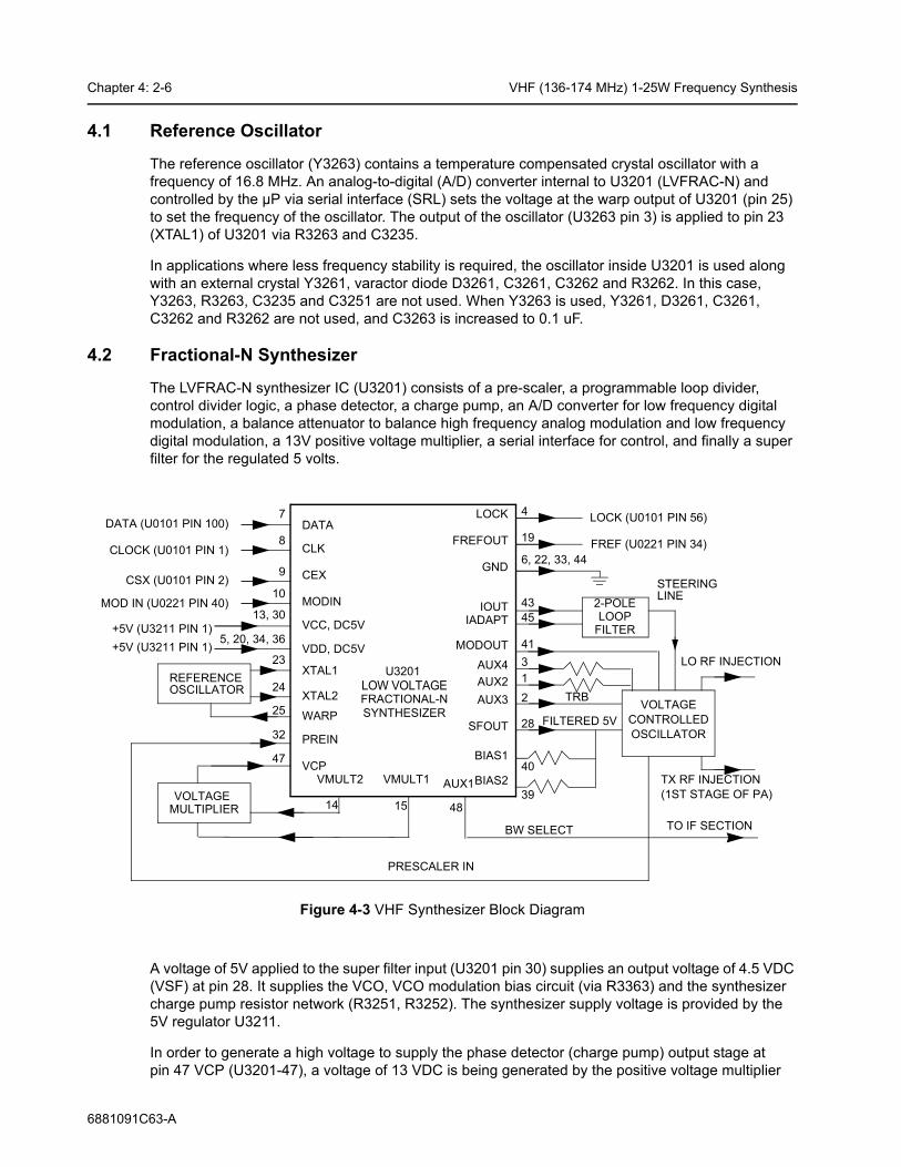
Chapter 4: 2-6 VHF (136-174 MHz) 1-25W Frequency Synthesis
4.1 Reference Oscillator
The reference oscillator (Y3263) contains a temperature compensated crystal oscillator with a frequency of 16.8 MHz. An analog-to-digital (A/D) converter internal to U3201 (LVFRAC-N) and controlled by the µP via serial interface (SRL) sets the voltage at the warp output of U3201 (pin 25) to set the frequency of the oscillator. The output of the oscillator (U3263 pin 3) is applied to pin 23 (XTAL1) of U3201 via R3263 and C3235.
In applications where less frequency stability is required, the oscillator inside U3201 is used along with an external crystal Y3261, varactor diode D3261, C3261, C3262 and R3262. In this case, Y3263, R3263, C3235 and C3251 are not used. When Y3263 is used, Y3261, D3261, C3261, C3262 and R3262 are not used, and C3263 is increased to 0.1 uF.
4.2 Fractional-N Synthesizer
The LVFRAC-N synthesizer IC (U3201) consists of a pre-scaler, a programmable loop divider, control divider logic, a phase detector, a charge pump, an A/D converter for low frequency digital modulation, a balance attenuator to balance high frequency analog modulation and low frequency digital modulation, a 13V positive voltage multiplier, a serial interface for control, and finally a super filter for the regulated 5 volts.
Figure 4-3 VHF Synthesizer Block Diagram
A voltage of 5V applied to the super filter input (U3201 pin 30) supplies an output voltage of 4.5 VDC (VSF) at pin 28. It supplies the VCO, VCO modulation bias circuit (via R3363) and the synthesizer charge pump resistor network (R3251, R3252). The synthesizer supply voltage is provided by the 5V regulator U3211.
In order to generate a high voltage to supply the phase detector (charge pump) output stage at pin 47 VCP (U3201-47), a voltage of 13 VDC is being generated by the positive voltage multiplier
DATA
CLK
CEX
MODIN
VCC, DC5V
XTAL1
XTAL2
WARP
PREIN
VCP
REFERENCEOSCILLATOR
VOLTAGEMULTIPLIER
DATA (U0101 PIN 100)
CLOCK (U0101 PIN 1)
CSX (U0101 PIN 2)
MOD IN (U0221 PIN 40)
+5V (U3211 PIN 1)
7
8
9
10
13, 30
23
24
25
32
47
VMULT2 VMULT1
BIAS1
SFOUT
AUX3
AUX4
IADAPTIOUT
GND
FREFOUT
LOCK 4
19
6, 22, 33, 44
4345
3
2
28
14 15
40
FILTERED 5V
STEERING
LOCK (U0101 PIN 56)
PRESCALER IN
FREF (U0221 PIN 34)
39BIAS2
41
48
5, 20, 34, 36+5V (U3211 PIN 1)
AUX1
VDD, DC5V MODOUT
U3201 LOW VOLTAGEFRACTIONAL-NSYNTHESIZER
AUX2
BW SELECT
TX RF INJECTION(1ST STAGE OF PA)
LO RF INJECTION
VOLTAGE CONTROLLED OSCILLATOR
LINE2-POLELOOP
FILTER
1TRB
TO IF SECTION
6881091C63-A
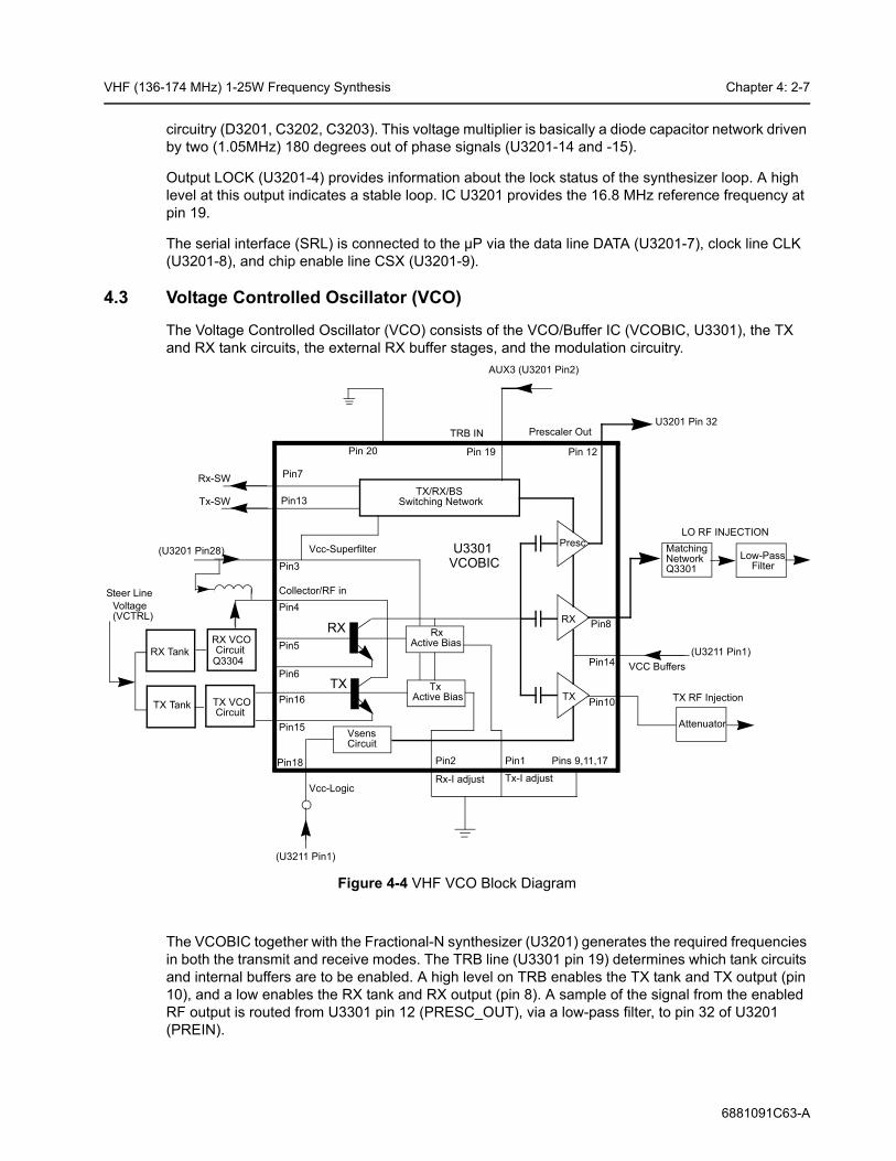
VHF (136-174 MHz) 1-25W Frequency Synthesis Chapter 4: 2-7
circuitry (D3201, C3202, C3203). This voltage multiplier is basically a diode capacitor network driven by two (1.05MHz) 180 degrees out of phase signals (U3201-14 and -15).
Output LOCK (U3201-4) provides information about the lock status of the synthesizer loop. A high level at this output indicates a stable loop. IC U3201 provides the 16.8 MHz reference frequency at pin 19.
The serial interface (SRL) is connected to the µP via the data line DATA (U3201-7), clock line CLK (U3201-8), and chip enable line CSX (U3201-9).
4.3 Voltage Controlled Oscillator (VCO)
The Voltage Controlled Oscillator (VCO) consists of the VCO/Buffer IC (VCOBIC, U3301), the TX and RX tank circuits, the external RX buffer stages, and the modulation circuitry.
Figure 4-4 VHF VCO Block Diagram
The VCOBIC together with the Fractional-N synthesizer (U3201) generates the required frequencies in both the transmit and receive modes. The TRB line (U3301 pin 19) determines which tank circuits and internal buffers are to be enabled. A high level on TRB enables the TX tank and TX output (pin 10), and a low enables the RX tank and RX output (pin 8). A sample of the signal from the enabled RF output is routed from U3301 pin 12 (PRESC_OUT), via a low-pass filter, to pin 32 of U3201 (PREIN).
Presc
RX
TX
MatchingNetwork Low-Pass
Filter
Attenuator
Pin8
Pin14
Pin10
(U3211 Pin1)VCC Buffers
TX RF Injection
U3201 Pin 32
AUX3 (U3201 Pin2)
Prescaler Out
Pin 12Pin 19Pin 20
TX/RX/BSSwitching Network
U3301VCOBIC
RxActive Bias
TxActive Bias
Pin2
Rx-I adjust
Pin1
Tx-I adjust
Pins 9,11,17Pin18
VsensCircuit
Pin15
Pin16
RX VCO Circuit
TX VCO Circuit
RX Tank
TX Tank
Pin7
Vcc-Superfilter
Collector/RF inPin4
Pin5
Pin6
RX
TX
(U3201 Pin28)
Rx-SW
Tx-SW
Vcc-Logic
(U3211 Pin1)
Steer Line Voltage (VCTRL)
Pin13
Pin3
TRB IN
LO RF INJECTION
Q3304
Q3301
6881091C63-A

Chapter 4: 2-8 VHF (136-174 MHz) 1-25W Frequency Synthesis
A steering line voltage (VCTRL) between 2.5V and 11V at varactor diode D3361 will tune the full TX frequency range (TXINJ) from 136 MHz to 174 MHz, and at varactor diode D3341 will tune the full RX frequency range (RXINJ) from 181 MHz to 219 MHz. The RX tank circuit uses a Hartley configuration for wider bandwidth. For the RX tank circuit, an external transistor Q3304 is used for better side-band noise.
The external RX buffers (Q3301 and Q3302) are enabled by a high at U3301 pin 7 (RX_SWITCH) via transistor switch Q3303. In the TX mode, the modulation signal (VCOMOD) from the LVFRAC-N synthesizer IC (U3201 pin 41) is applied to varactor diode D3362, which modulates the TX VCO frequency via capacitor C3362. Varactor D3362 is biased for linearity from VSF.
4.4 Synthesizer Operation
The complete synthesizer subsystem consists of the low voltage FRAC-N (LVFRACN), the reference oscillator (a crystal oscillator with temperature compensation), charge pump circuitry, loop filter circuitry and a DC supply. The output signal PRESC from the VCOBIC (U3301 pin 12) is fed to U3201 pin 32 (PREIN) via a low-pass filter (C3318, L3318 and C3226) which attenuates harmonics and provides the correct level to close the synthesizer loop.
The pre-scaler in the synthesizer (U3201) is a dual modulus type with selectable divider ratios. The divider ratio of the pre-scaler is controlled by the loop divider, which in turn receives its inputs via the SRL. The output of the pre-scaler is applied to the loop divider. The output of the loop divider is connected to the phase detector, which compares the loop divider’s output signal with the reference signal. The reference signal is generated by dividing down the signal of the reference oscillator (Y3261 or Y3263).
The output signal of the phase detector is a pulsed DC signal which is routed to the charge pump. The charge pump outputs a current at U3201 pin 43 (IOUT). The loop filter (which consists of R3221-R3223 and C3221-C3224) transforms this current into a voltage that is applied to the varactor diodes (D3361 for transmit, D3341 for receive) to alter the output frequency of the appropriate VCO. The current can be set to a value fixed within the LVFRAC-N IC, or to a value determined by the currents flowing into BIAS 1 (U3201-40) or BIAS 2 (U3201-39). The currents are set by the value of R3251 and R3252 respectively. The selection of the three different bias sources is done by software programming.
To reduce synthesizer lock time when new frequency data has been loaded into the synthesizer, the magnitude of the loop current is increased by enabling the IADAPT pin (U3201-45) for a certain software programmable time (adapt mode). The adapt mode timer is started by a low to high transition of the CSX line. When the synthesizer is within the lock range, the current is determined only by the resistors connected to BIAS 1 and BIAS 2, or by the internal current source. A settled synthesizer loop is indicated by a high level signal at U3201-4 (LOCK).
The LOCK signal is routed to one of the µP’s ADC inputs (U0101-56). From the measured voltage, the µP determines whether LOCK is active.
In order to modulate the PLL, the two spot modulation method is utilized. Via U3201 pin 10 (MODIN), the audio signal is applied to both the A/D converter (low frequency path) as well as the balance attenuator (high frequency path). The A/D converter changes the low frequency analog modulating signal into a digital code that is applied to the loop divider, thereby causing the carrier to deviate. The balance attenuator is used to adjust the VCO’s deviation sensitivity to high frequency modulating signals. The output of the balance attenuator is present at the MODOUT port (U3201-41) and connected to the VCO modulation diode D3362 via R3364.
6881091C63-A
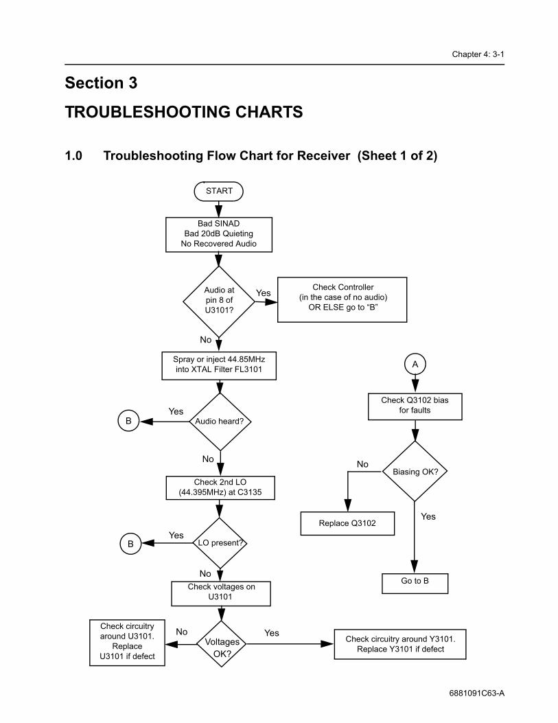
Chapter 4: 3-1
Section 3TROUBLESHOOTING CHARTS
1.0 Troubleshooting Flow Chart for Receiver (Sheet 1 of 2)
Bad SINADBad 20dB Quieting
No Recovered Audio
START
Audio at pin 8 of U3101?
Check Controller(in the case of no audio)
OR ELSE go to “B” Yes
No
Spray or inject 44.85MHz into XTAL Filter FL3101
Audio heard?BYes
No
Check 2nd LO (44.395MHz) at C3135
LO present?BYes
Check voltages on U3101
Biasing OK?
No
No
A
Yes
Check Q3102 bias for faults
Replace Q3102
Go to B
Yes
No
Check circuitry around U3101.
Replace U3101 if defect
Check circuitry around Y3101. Replace Y3101 if defect
Voltages OK?
6881091C63-A

Chapter 4: 3-2 Troubleshooting Flow Chart for Receiver
1.1 Troubleshooting Flow Chart for Receiver (Sheet 2 of 2)
IF Signal at C3035?
No
RF Signal at T3001?
RF Signal at C3012?
No
RF Signal at C3008?
No
RF Signal at C3474?
No or
Check Harmonic Filter J3401 and
Antenna Switch D3471,D3472,L3472
Check filter between C3474 & C3008. Check tuning
voltage at R3019
Inject RF into J3401
Is tuning voltage OK?
No
Yes
Check RF amp (Q3001) Stage
Check filter between C3012 & T3001
Yes
Check T3001, T3002, D3031, R3030-R3034,
L3032, C3034 and C3035Yes
1st LO level OK?
Locked?
YesCheck FGU
Yes
Trace IF signal from C3035 to Q3101.
Check for bad XTAL filter
No
YesIF signal at Q3102
collector?
Before replacing U3101, check
U3101 voltages
Yes
Check for 5VDC
Is 9.3V present?
Check Supply Voltage circuitry. Check Q0681,
U3211 and U0641
No
No
No
Check U3501
Check varactor filter
No
Yes
Yes
Yes
A
A
B
weak RF
6881091C63-A
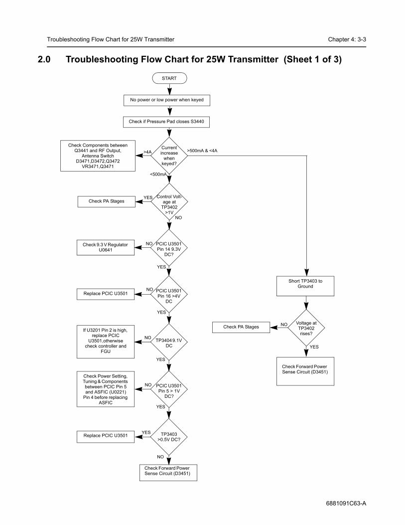
Troubleshooting Flow Chart for 25W Transmitter Chapter 4: 3-3
2.0 Troubleshooting Flow Chart for 25W Transmitter (Sheet 1 of 3)
Current increase
when keyed?
NO
YES
START
Check if Pressure Pad closes S3440
Check Components between Q3441 and RF Output,
Antenna Switch D3471,D3472,Q3472
VR3471,Q3471
>500mA & <4A>4A
<500mA
Check PA StagesControl Volt-
age at TP3402
>1V
Short TP3403 to Ground
NO
YES
Voltage at TP3402 rises?
Check PA Stages NO
YES
PCIC U3501 Pin 14 9.3V
DC?
Check 9.3 V Regulator U0641
NO
YES
PCIC U3501 Pin 16 >4V
DC
Replace PCIC U3501
NO
YES
TP3404 9.1V DC
If U3201 Pin 2 is high, replace PCIC
U3501,otherwise check controller and
FGU
YES
NO
TP3403 >0.5V DC?
Replace PCIC U3501
Check Forward Power Sense Circuit (D3451)
Check Forward Power Sense Circuit (D3451)
NO
YES
PCIC U3501 Pin 5 > 1V
DC?
Check Power Setting, Tuning & Components between PCIC Pin 5 and ASFIC (U0221)
Pin 4 before replacing ASFIC
No power or low power when keyed
6881091C63-A

Chapter 4: 3-4 Troubleshooting Flow Chart for 25W Transmitter
2.1 Troubleshooting Flow Chart for 25W Transmitter (Sheet 2 of 3)
Check PA Stages
No power or low power when keyed
Measure DC Voltage at Pin 2 & 3 of U3401
>6
YES
DC Voltage at U3501
Pin 23 =0?
2-6
DC Voltage at U3402-1
Pin 1?
YES
Pin 2 Volt-age 0.62 * Voltage at
Pin 1?
If U3201 Pin 2 is high, replace PCIC
NOReplace U3401
YES
NODC
Voltage at U3402-1 Pin
3 = 8.8V?
Check S3440, R3442 and R3443
YES
Pin 3 Volt-age 0.51 * Voltage at
Pin 1?
NOReplace U3401
<2V DC Voltage at U3402-2
Pin 7?
>6VCheck Components
between U3402-2 Pin 7 and Q3421. Check
Resistive Network at Pins 5 & 6 before replacing Q3421
YES
DC Voltage at U3402-2
Pin 5 <8.8V?
Check Components between U3402-2 Pin 7
and Q3421. Check Resis-tive Network at Pins 5 & 6 before replacing Q3421
NO
Check Q3422
NO
Check Final PA Stage
2-6V
<2VCheck Resistive Net-work at Pins 2 & 3 of
U3402-1 before replac-ing U3401
Check Q3442 and Resistive Network at
U3402-1 Pin 3 before replacing
U3401
6881091C63-A

Troubleshooting Flow Chart for 25W Transmitter Chapter 4: 3-5
2.2 Troubleshooting Flow Chart for 25W Transmitter (Sheet 3 of 3)
Check Final PA Stage
NO
0V
1-4V
Bias 2 DC Voltage at TP3406?
YES
RF Voltage at TP3401 >100mV?
YES
RF Voltage U3401 Pin 6
>3V?
Supply
Replace Q3441
Check FGU (U3301)
NO Check Components between TP3401 &
C3417
NO
YES ASFIC U0221 Pin 6
1-4V DC?
Check Bias Tuning before replacing ASFIC
U0221
Check Components between ASFIC and
Q3441 before replacing Q3441
YES
RF Voltage Q3421 Gate
>1V?
NO Check Components between C3417 &
Q3421
YES
RF Voltage Q3441 Gate
>4V?
NO Check Components between Q3421 &
Q3441
Check Components between Q3441 &
Antenna Connector
Voltage
6881091C63-A
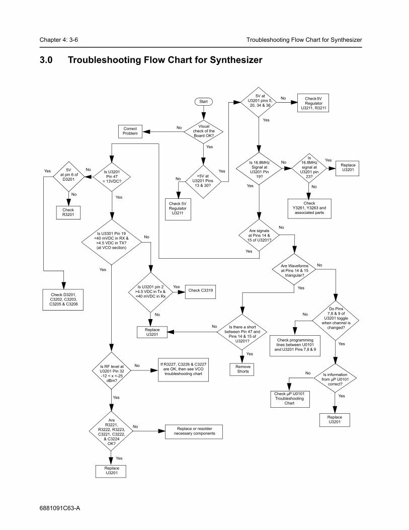
Chapter 4: 3-6 Troubleshooting Flow Chart for Synthesizer
3.0 Troubleshooting Flow Chart for Synthesizer
+5V at U3201 Pins
13 & 30?
5V at pin 6 of
D3201
Is informationfrom µP U0101
correct?
Is U3201 Pin 47
= 13VDC?
Is U3301 Pin 19<40 mVDC in RX &>4.5 VDC in TX? (at VCO section)
Start
Visual check of the Board OK?
CorrectProblem
Check 5VRegulator
U3211
Is 16.8MHzSignal at
U3201 Pin 19?
CheckY3261, Y3263 and associated parts
Are signalsat Pins 14 &
15 of U3201?
Check R3201
Check C3319Is U3201 pin 2
>4.5 VDC in Tx & <40 mVDC in Rx
Replace U3201
RemoveShorts
Is there a shortbetween Pin 47 and
Pins 14 & 15 ofU3201?
Replace or resoldernecessary components
Is RF level atU3201 Pin 32 -12 < x <-25
dBm?
Are R3221,
R3222, R3223, C3221, C3222,
& C3224 OK?
Replace U3201
If R3227, C3226 & C3227are OK, then see VCOtroubleshooting chart
Are Waveformsat Pins 14 & 15
triangular?
Do Pins 7,8 & 9 of
U3201 togglewhen channel is
changed?
Check programminglines between U0101
and U3201 Pins 7,8 & 9
Replace U3201
Check µP U0101Troubleshooting
Chart
No
Yes
No
Yes
No
Yes
No
No
No
Yes
Yes
No
Yes
Yes
No
Yes
Yes
Yes
No
No
No
No
Yes
No
Yes
Yes
Check D3201, C3202, C3203, C3205 & C3206
5V at U3201 pins 5, 20, 34 & 36
Check 5V Regulator
U3211, R3211
Is 16.8MHz signal at
U3201 pin 23?
Replace U3201
Yes
No
No
Yes
No
Yes
6881091C63-A
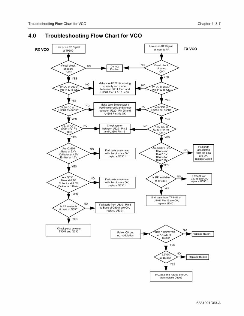
Troubleshooting Flow Chart for VCO Chapter 4: 3-7
4.0 Troubleshooting Flow Chart for VCO
Are Q3301Base at 0.7V
Collector at 4.5V Emitter at 110mV
Are Q3304Base at 2.4V
Collector at 4.5V Emitter at 1.7V
Are U3301 Pins13 at 4.4V15 at 1.1V10 at 4.5V16 at 1.9V
Low or no RF Signalat TP3001
Visual checkof board
OK?
35mV DC atU3301 Pin 19
NO
YES
at base of Q3301
NO
NO
NO
NO
NO
YES
YES
YES
YES
YES
Low or no RF Signalat input to PA
5V DC at U3301Pin 14 & 18 OK?
4.8V DC atU3301 Pin 19
Is RF available at TP3401
YES
YES
YES
YES
YES
NO
NO
NO
NO
NO
Audio =180mVrmsat “-” side of
D3362
2.5VDCat D3362
If C3362 and R3363 are OK, then replace D3362
Replace R3363
Replace R3364
NO
NO
YES
YES
If R3402 and C3315 are OK,replace U3301
TX VCORX VCO
CorrectProblem
Visual checkof board
OK?
Make sure U3211 is working correctly and runner
between U3211 Pin 1 and U3301 Pin 14 & 18 is OK
Check runner between U3201 Pin 2
and U3301 Pin 19
Is RF available If all parts from U3301 Pin 8to Base of Q3301 are OK,
replace U3301
If all parts associated with the pins are OK,
replace Q3301
Check parts between T3001 and Q3301 Power OK but
no modulation
If all parts from TP3401 of U3401 Pin 16 are OK,
replace U3401
If all parts associated
with the pins are OK,
replace U3301
4.5V DC atU3301 Pin 3 OK?
YES
NO 4.5V DC atU3301 Pin 3 OK?
YES
NOMake sure Synthesizer is
working correctly and runner between U3201 Pin 28 and
U4301 Pin 3 is OK
5V DC at U3301Pin 14 & 18 OK?
OK? OK?
If all parts associated with the pins are OK,
replace Q3301
6881091C63-A
Chapter 4: 3-8 Troubleshooting Flow Chart for VCO
Notes
6881091C63-A
Chapter 4: 4-1
Section 4VHF (136-174 MHZ) 1-25W PCBS, SCHEMATICS, ANDPARTS LISTS
1.0 Allocation of Schematics and Circuit Boards1.1 Controller Circuits
The VHF circuits are contained on the printed circuit board (PCB) which also contains the controller circuits. This chapter shows the schematics for the VHF circuits only. Refer to the controller section for details of the related controller circuits. The PCB component layouts and the parts lists in this chapter show both the controller and VHF circuit components. The VHF schematics and the related PCB and parts list are shown in the tables below.
Table 4-1 VHF 1-25W PCB 8486172B04 Diagrams and Parts ListsPCB 8486172B04:Main Board Top SideMain Board Bottom Side
Page: 4: 4-34: 4-4
SCHEMATICSPower Amplifier 1 - 25WFRACN SynthesizerVoltage Controlled OscillatorReceiver Front-EndIF
4: 4-54: 4-64: 4-74: 4-84: 4-9
Parts List 4: 4-10Controller version is T2
Table 4-2 VHF 1-25W PCB 8486172B06 Diagrams and Parts ListsPCB 8486172B06:Main Board Top SideMain Board Bottom Side
Page: 4: 4-134: 4-14
SCHEMATICSPower Amplifier 1 - 25WFRACN SynthesizerVoltage Controlled OscillatorReceiver Front-EndIF
4: 4-154: 4-164: 4-174: 4-184: 4-19
Parts List 4: 4-20Controller version is T5
6881091C63-A
Chapter 4: 4-2 Allocation of Schematics and Circuit Boards
Table 4-3 VHF 1-25W PCB 8486172B07 Diagrams and Parts ListsPCB 8486172B07:Main Board Top SideMain Board Bottom Side
Page: 4: 4-234: 4-24
SCHEMATICSPower Amplifier 1 - 25WFRACN SynthesizerVoltage Controlled OscillatorReceiver Front-EndIF
4: 4-154: 4-254: 4-174: 4-184: 4-26
Parts List 4: 4-27Controller version is T7
Table 4-4 VHF 1-25W PCB 8486172B08 Diagrams and Parts ListsPCB 8486172B08:Main Board Top SideMain Board Bottom Side
Page: 4: 4-304: 4-31
SCHEMATICSPower Amplifier 1 - 25WFRACN SynthesizerVoltage Controlled OscillatorReceiver Front-EndIF
4: 4-324: 4-254: 4-174: 4-184: 4-33
Parts List 4: 4-34Controller version is T9
6881091C63-A

VHF (136-174 MHz) 1-25W PCB 8486172B04, Schematics, and Parts Lists Chapter 4: 4-3
6881091C63-A
2
C3002
C3
00
4
C3
00
5
C3
00
6
C3007
C3008
C3009
C3010
C3
011
C3012
C3013
C3014
C3
01
5
C3
01
6
C3
01
7
C3
01
8
C3019C3020
C3027
C3
02
8
C3034
C3
10
0C
31
01
C3
10
2
C3
10
3
C3114
C3115
C3131
C3
13
2
C3133
C3
13
4
C3135
C3
13
6C
31
37
C3
13
9
C3
14
0C
31
41
C3
14
2
C3143 C3144
C3
14
5
C3444
C3446
C3
44
7
C3472
C3473
C3474
C3497
D3001
D3003
D3004
D3
47
1
D3
47
2
23
45
6
FL3101
23
45
6
FL3102
4
3 2
FL3112
FL3114
2 3
J3401
L3
00
2
L3031
L3032
L3100
L3
10
1
L3443
L3471
L3472
L3493
Q3001
Q3
02
1
R3001
R3002
R3003
R3
00
4
R3
00
5
R3009
R3013
R3014
R3015
R3016
R3024
R3025
R3031
R3
10
1
R3
10
6
R3111
R3117
R3130
R3
13
2
R3144
R3
14
5
R3491
11
120
10
U3101
8 7
114
U3111
8 7
114
U31152
Y3102
3
1
WA
RIS
VH
F R
F 1
-25
W
To
p s
ide
84
86
17
2B
04
-P4
CH
EC
KO
NE
O.K
. A
S IS
O.K
. A
S M
AR
KE
D
( )
( )
ISS
.R
EV
ISIO
NR
LS
E.
CO
RR
EC
TE
DA
SM
AR
KE
D
ILLU
ST
RA
TO
RD
AT
EE
NG
INE
ER
DA
TE
PR
OG
RA
MD
ISK
RL
SE
.
DW
G. N
O.
LE
TT
ER
ING
SIZ
E:
RE
QU
IRE
S:
ED
ITO
RD
AT
EC
HE
CK
ER
DA
TE
Illu
str
ato
rR
K7. O
ct 1999
ZW
G0
13
03
97
P4
ZWG0130397-P4
VHF (136-174 MHz) 1-25W PCB 8486172B04 Top Side
ZWG0130397-P4
.0 VHF (136-174 MHz) 1-25W PCB 8486172B04, Schematics, and Parts Lists
C0101 C0102
C0104
C0
10
5
C0
10
6
C0107
C0
12
1
C0131
C0132
C0
211
C0212
C0
22
1
C0
22
2
C0223
C0
22
4
C0
22
5
C0226
C0227
C0
23
1
C0232
C0
23
3
C0234
C0235
C0236
C0
23
7
C0241
C0242
C0243
C0244
C0245
C0246
C0251
C0252
C0253
C0
25
5
C0261
C0262
C0267
C0
42
1
C0
44
1
C0
44
2
C0
44
3
C0
44
4
C0
44
5
C0
44
6
C0
44
7
C0
44
8
C0
44
9
C0
45
1
C0
45
2
C0
45
3
C0
45
4
C0
45
5
C0
45
6
C0
45
7
C0
45
8
C0
45
9
C0
46
0
C0
46
1
C0
46
2
C0
46
3
C0
46
4
C0
46
6
C0
46
7
C0
46
8
C0
47
0
C0
47
1
C0
47
2
C0
47
3
C0
47
4
C0
47
6
C0
47
7
C0
47
8
C0
48
2
C0
48
3
C0484
C0
48
6
C0
48
7
C0
48
8
C0
49
0
C0
49
3
C0
49
4
C0
49
5
C0496
C0
50
1
C0
50
2
C0
50
3
C0
50
4
C0
50
5
C0
50
6
C0
50
8
C0
50
9
C0
51
0
C0
511
C0
51
2
C0
51
3
C0
51
4
C0
51
5
C0
51
6
C0
51
7
C0
51
8
C0
51
9
C0
52
0
C0
52
1
C0
52
2
C0
52
3
C0
52
4
C0
52
5
C0
52
6
C0
52
7
C0
52
8
C0
53
0
C0531
C0
53
2
C0
53
3
C0
53
4
C0
53
5
C0
53
6
C0
53
7
C0538
C0
53
9
C0
54
0
C0542
C0601
C0603
C0612
C0651
C0652
C0654C0655
C0681
C3021
C3032
C3209
C3210
C3211
C3213
C3214C3215
C3221C3222
C3223 C3224
C3226
C3
22
7 C3229
C3231
C3
23
2
C3
23
3C
32
34
C3
23
5
C3242
C3243
C3244
C3245
C3246
C3
25
2
C3
25
3C
32
54
C3255
C3324
C3336
C3337
C3341
C3
34
2
C3344
C3
34
5
C3346 C3347
C3357
C3361
C3362C3363
C3364
C3365
C3400
C3401
C3403C3404
C3410
C3411
C3412
C3417
C3418
C3
41
9
C3420
C3422
C3423
C3
42
4
C3425
C3
42
6
C3428
C3
43
1
C3432
C3433
C3
43
4
C3
43
5
C3441C3442
C3443
C3445
C3448
C3449
C3453
C3
50
7
C3
50
8
C3509
D0201
D0
65
1
D3031
D3221
D3
34
1
D3361
D3362
D3401
1 18
J0451
2011
10
J0501
J0601
L0481
L0482
L3
03
4
L3201 L3232
L3333
L3341
L3343 L3344
L3346
L3361
L3362
L3363
L3364
L3401
L3403
L3411
L3412L
34
13
L3
41
4
L3422
M3421
Q0110
Q0177Q0181Q0185
Q0681
Q3221
Q3304
Q3411
Q3422
2
3
4
5
6
7
8
Q3441
Q3
44
2
Q3471Q3472
R0101
R0102
R0
10
4
R0105
R0106
R0
10
8
R0
10
9
R0110
R0114
R0
11
5
R0116
R0128
R0131
R0132
R0170
R0181
R0182
R0185
R0186
R0211
R0212
R0
22
0
R0
22
1
R0
22
2
R0223
R0224
R0225
R0226
R0
22
7
R0241
R0242
R0251
R0252
R0253
R0
26
1
R0
26
2
R0267
R0
26
8
R0269
R0510
R0522
R0524
R0528
R0533R0535
R0538
R0539
R0611
R0
61
2
R0651
R0652
R0681
R0
68
2
R3211
R3221
R3222R3223
R3224
R3225
R3227
R3242
R3
25
1
R3
25
2
R3
26
3
R3335
R3
33
6
R3341R3
34
2
R3361
R3362
R3
36
3R3364
R3
40
0
R3401
R3402
R3403
R3
40
4
R3405
R3406
R3414
R3415
R3
41
6
R3
42
4
R3
42
5
R3
42
6
R3
42
7
R3431R3432
R3433
R3434
R3435
R3471
R3473
R3505
R3506
R3507
R3508
R3509
SH3301
3
4 6
12
T3001
3
46
12
T3002
TP3401
1
7651
26
U0101
3217
161
U0121
87
1 14
U0211
1 37
2513
U0221
161
8 9
U0251
9
U0271
1
6
5
U0611
1
6
5
U0641
3
2
1
U0651
45
8
U3211
1
16
8
9
U3401
U3502
VR
05
01
VR0503VR0505
VR0510
2 3
4
Y0131
1
1
48
1
100
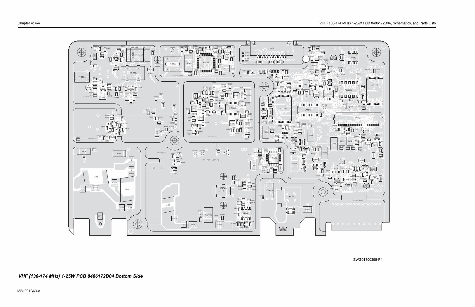
Chapter 4: 4-4 VHF (136-174 MHz) 1-25W PCB 8486172B04, Schematics, and Parts Lists
6881091
C0103
C0111
C0112
C0122C0123
C0125
C0141
C0151
C0201
C0203C 0204
C0205
C0254C0265
C0266
C0271C0272
C0273
C0274
C0275
C0276 C0277
C03
41
C0342
43
C0344
C0541
C0554
C0558
C0559C0560 C0575
C0576
C0591
C0592
C0593
C0621
C0622
C0641
C0644
C0645
C0661
C0662
C0663
C0671
D01
01
D0151
D0179
D06
21
D06
60D
0661
E0271 E0272
E0631
140
J0551
Q01
51
Q0171
Q0173 Q0183
Q0271
Q0641
Q06
61
Q0662Q0663
R0107
R0111
R0112
R0113R0117
R0121
R0124
R0125R0126
R0127
R0151R0152
R0171R0172R0173
R0174
R0175
R0176R0177
R0178
R0179
R0183
R0184
R0201
R0202
R0204
R 0205
R0206
R0207
R0208
R0265
R0266
R0273
R0274R0275
R0276
23
R0333
R0341
R0342
344R0345
R0346 R0347
R0401
R0408
R0511
R0512
R0521
R0523 R0525
R0527
R0529
R0530
R0531R0537
R0541
R0542
R0591
R0592
R0621
R0641
R0642R0643
R0661
R0662 R0671 R0672
TP0101
TP0102
TP0103
TP0151
TP0221
TP0222
TP0481
14
5 8
U0111
22
21 8
71
U0122
1 14
1528
U0125
16
18
9
U0141
15
14
1
4 5
8
U0341
U0342
1 4
58
U0652
U06
53
VR
0151
VR0504 VR0509
VR0521
VR0522
VR
0537
VR0541
R0601
VR
0621
VR0671
CNTL-REV-T2
ZWG0130398-P4
VHF (
ZWG01300398-P4
C63-A
C03
01
C0302
C0303
C0304C0305
C0324 C0325
C03
C0351
C0352
C0353
C0354
C04
01
C04
02
C04
03
C04
06
C04
07
C04
08
C04
09
C04
10
C04
11
C04
22
C04
23
C04
26
C04
27
C04
28
C04
29 C0430 C0431C0485
C0491
C0492
C0497
C0498
C0499
C0611
C3000
C3001
C3003C3022
C3023
C3024
C3025
C3026
C3029
C3031
C3033
C3035
C3104
C3110C3111
C3112
C3113
C3116
C3121
C3122C 3123
C31
38
C3146
C3147
C3151
C3152
C3155
C3202C 3203
C3205C3206
C3207
C3208 C3212
C3225
C3228
C3241
C3251
C3261
C 3
262
C3263
C 3301
C3302
C3303
C3304
C3305
C3306 C3311
C3312
C33
13
C3314
C3315
C3316
C3317
C3318
C3319
C3331
C3332
C3333C3334
C3335
C3348
C3351
C3352
C3355
C3356
C3402
C3405C3406
C3413
C3414C3415
C3416
C3421
C3427
C3436C3437
C3438
C3439
C3440
C3451
C3452
C3471
C3475
C34
91C
3492
C3493
C3494
C3495C3496
C3498
C3499
C 3501
C3502
C3503
C3504
C35
05
C3506
C3510
D03
01
D3000
D30
11
D3101
D3201
D3261
D3451
4 3
2
FL3111
FL3
113
4 3
2
FL3115 12
J0401
L302
5
L3111L3112
L3231
L3301
L3302
L331
1
L3317
L3318
L3331
L3332
L3345
L3351
L3402
L3421
L3436
L3437
L3491
L3492
Q0331
Q30
02
Q3101Q3102
Q3151
Q3152
Q3155
Q3301
Q3302
4 3
Q3303
1 23
Q3421
R03
R0324
R0331 R0332
R0334
R0
R0407 R0409 R0410
R0467
R0468
R0481
R0482
R3000
R3006
R3010
R3011
R3012
R3018
R3019
R3020R3021
R3022
R3023
R3030
R3032
R3033
R3034
R3035
R3036
R3102R3104R3105
R3107R3108
R3112
R3113
R3114
R 3115
R 3116R3118
R3133
R3134
R3135
R3146
R3147
R3151
R3152
R3153
R3154
R3155
R 3201R3203
R3204
R3206
R3226
R3228
R 3
241
R3261
R 3
262
R3301
R3302
R3303R3304
R 3305
R3306R3307
R3308
R3311
R3312
R3313
R3314
R33
15
R3316
R3317
R3318
R33
19
R3321
R3323
R3331
R3343
R3351
R3352
R3353R3354
R3355
R3356
R3411
R3412
R3413
R3417
R3418
R3421
R3422R3423
R3428
R3429
R3441
R3442R3443
R3444
R3445
R3446R3452
R3454
R3455
R3457R3474
R3475
R3501
R3502 R3504
TP3201TP3202
TP3402
TP3403TP3404TP3405
TP3406
28
1
U0301
4
58U0351
137
25 13
U3201
11
1
20
10
U3301
14
5 8
U3402
1
17
9
25
U3501
V
VR
3471
43
2Y3101
Y3261
2
3 4
Y3263
1
1
48
15
11
32
1
1
8486172B04_P4
C99
PA-REV-P4
VCO-REV-T1
IF-REV-T3
FE-REV-T3
FRAC-REV-P7
136-174 MHz) 1-25W PCB 8486172B04 Bottom Side
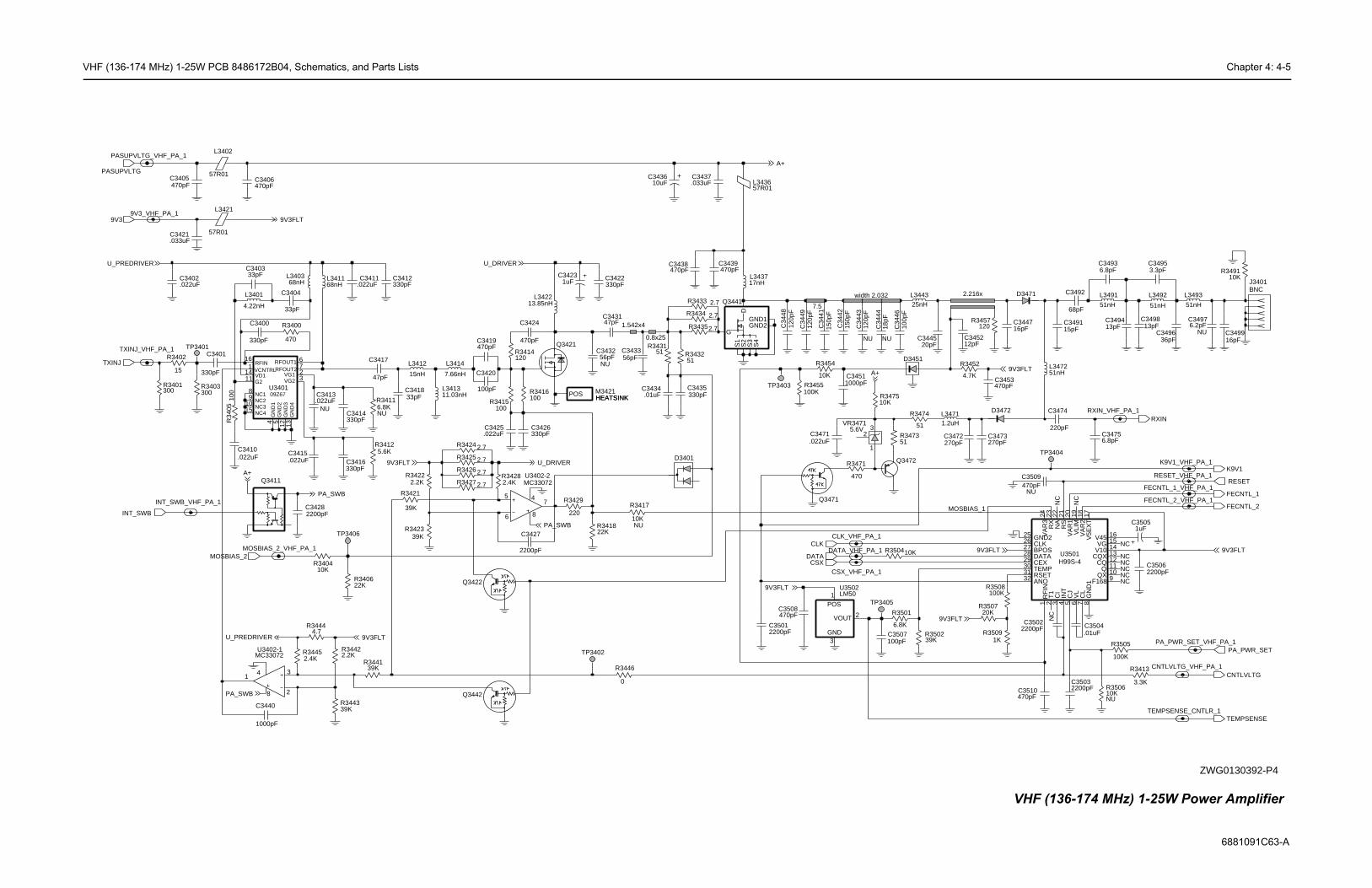
VHF (136-174 MHz) 1-25W PCB 8486172B04, Schematics, and Parts Lists Chapter 4: 4-5
6881091C63-A
J3401BNC
2.216xwidth 2.032
C35022200pF
.01uFC3504
2200pFC3503
RESET
RXIN_VHF_PA_1
R349110K
100pFC3507
RESET_VHF_PA_1
270pFC3473 C3475
6.8pF
C34
4418
pF
NU
C34
4312
0pF
NU
U3502
D
S
2OUT
LM50
C3492
68pF
C34936.8pF
Q3472
C35062200pF
C35051uF
39KR3502
R3501
6.8K
RXIN
120R3457
V5E
XT
20V
AR
1
18V
AR
2
24V
AR
3
VG 15
6V
L19
VLI
M
RF
IN
21R
S
31 RSET
23R
X2
T1
30 TEMP
14V10
16V45
17
DATA
9F168
8G
ND
1
25 GND2
4IN
T22
NA
11Q 10QX
1
BPOS29 CEX
3C
I
5C
J
7C
L
26 CLK
12CQCQX 1328
H99S-4U3501
32 ANO
27
LK_VHF_PA_1
L3443
25nH
R350410K
220pF
C3474
R3506
1.2uH
NU10K
L3471
TEMPSENSETEMPSENSE_CNTLR_1
20KR3507
R3509
PA_PWR_SET
1K
FECNTL_2
1000pFC3451
SX_VHF_PA_1
TA_VHF_PA_1
20pFC3445
R347510K
K9V1_VHF_PA_1K9V1
3.3pFC3495
R3471
470
C349636pF
C3497
NU6.2pF
51R3473
C349115pF
D3471
NU470pFC3509
R3508100K
R3505
100K
TP3405
FECNTL_1
CNTLVLTGR3413
3.3K
13pFC3499
C3498
16pF
FECNTL_1_VHF_PA_1
FECNTL_2_VHF_PA_1
13pFC3494
D3472
C34
4610
0pF
D3451
51nH
L3493
R3474
515.6V
23
1
VR3471
470pFC3510
CNTLVLTG_VHF_PA_1
PA_PWR_SET_VHF_PA_1
R3452
4.7K
C3472270pF
C3453470pF
TP3404
51nH
L3492L3491
51nH
L347251nH
C345212pF
16pFC3447
150p
FC
3442
1
9V3FLT
9V3FLTA+
NC
9V3FLT 9V3FLT
MOSBIAS_1
NC
NC
NC
NCNCNCNCNC
ZWG0130392-P4
VHF (136-174 MHz) 1-25W Power Amplifier
7.5
0.8x25
1.542x4
R343251
.033uFC3437
57R01L3436
C3419470pF
C34282200pF
2.7R3427
R3426 2.7
2.7R3425
2.4KR3428
C3427
2200pF
2.4K
MOSBIAS_2_VHF_PA_1
R3445
15nH
L3412
C3406470pF
300R3401
POSHEATSINKM3421HEATSINK
Q3421
330pFC3416
330pF
C3400 R3400
470
C3404
33pF
C3410.022uF
PASUPVLTG_VHF_PA_1
100R3415
33pFC3403
TP3403
TP3402
C3421.033uF
C3435330pF
R343151
CLK
2.7R3435
C3425.022uF
C343256pFNU
3GN
PO1
V
R3417
39K
NU10K
R3443
R344139K
R34422.2K
.01uFC3434
10KR3404
47pF
MOSBIAS_2
C3431
DATA
39K
R3421
R341822K
8
4
C3440
1000pF
U3402-1MC33072
2
31
2.7R3434
TXINJ
C
C34
4912
0pF
R3414120
C3426330pF
57R01
L3402
C
DA
C341833pF
C3422330pF
R34444.7
R3402
15
39KR3423
2.2KR3422
6
57
8
4
MC33072U3402-2
220
R3429
2.7R3433
C3508470pF
2200pFC3501
INT_SWB_VHF_PA_1
9V3
D3401
INT_SWB
TP3401
13.85nH
470pF
L3422
C3424 C34
4812
0pF
17nHL3437
.022uFC3471
C3411.022uF
R3403300
C3405470pF
22KR3406
L341311.03nH
5.6KR3412
NU6.8K
100
R3411
R34
05
2.7R3424
RFOUT1 6RFOUT2 7
VCNTRL1VD1
14 2VG1VG2 3
GN
D2
5G
ND
312
GN
D4
13
NC18NC29NC310NC415
RFIN16
U3401G211
GN
D1
4
330pF
09Z67
C3401C3417
47pF
C34
41
PASUPVLTG
150p
F
R3416100
68nHL3403
TXINJ_VHF_PA_1
9V3_VHF_PA_1
330pFC3412
4.22nH
L3401
470pFC3439
L341168nH
C3438470pF
R3454
10K
L3414
7.66nH
NU.022uFC3413
C34231uF
S3
S4
D
G
GND1GND2
S1
S2
Q3441
C3415.022uF
100pF
.022uF
C3420
C3402
R3455100K
C343610uF
56pFC3433
57R01
C3414
L3421
330pF
Q3411
TP3406
Q3422
Q3442
0
R3446
CSX
PA_SWB
A+
Q347
U_DRIVER
9V3FLT
PA_SWB
U_DRIVER9V3FLT
9V3FLT
A+
U_PREDRIVER
PA_SWB
9V3FLT
U_PREDRIVER
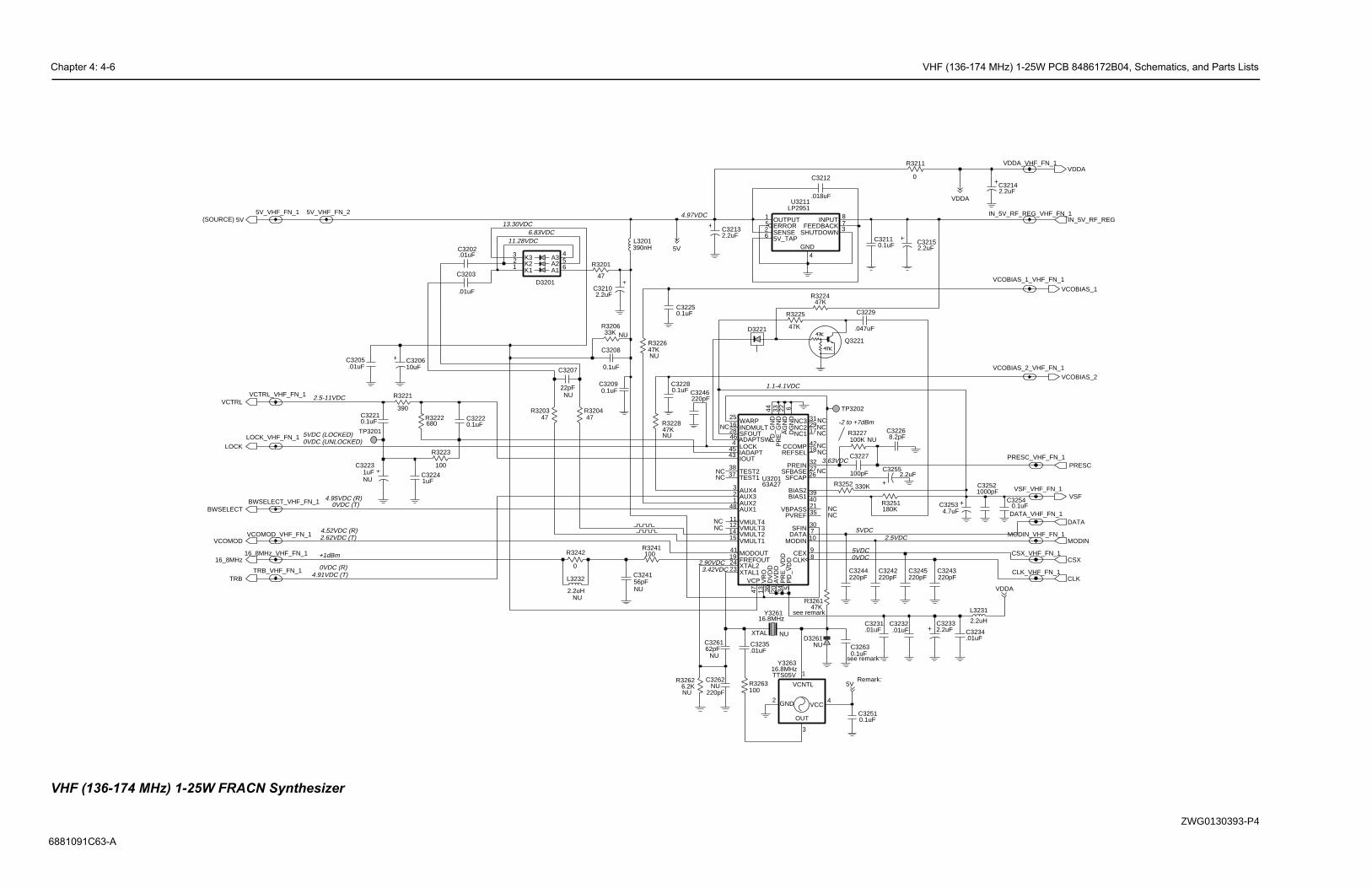
Chapter 4: 4-6 VHF (136-174 MHz) 1-25W PCB 8486172B04, Schematics, and Parts Lists
6881091
Remark:
If Y3261 is placed then C3263 2113740F07 1.5pF
If Y3263 is placed then C3263 2113743E20 100nFRxxx 0662057B02 150k
R3261 0662057A89 47k
see remark
C3245220pF
378
2.2uFC3255
C32521000pF
DATA
2.2uFC3233
MODIN_VHF_FN_1
IN_5V_RF_REG
.01uFC3234
C3244220pF
2.2uFC3215
100pF
C3227
CSX
MODIN
0.1uFC3263
VSF
VCOBIAS_1
C32510.1uF
TP3202
220pFC3243
VCOBIAS_2_VHF_FN_1
C3253
VCOBIAS_2
4.7uF
C32268.2pF
CLK
PRESC_VHF_FN_1
CSX_VHF_FN_1
VSF_VHF_FN_1
R3227
C3254
NU100K
0.1uFDATA_VHF_FN_1
VDDAVDDA_VHF_FN_1
C3214
PRESC
2.2uF
220pFC3242
3252
VCOBIAS_1_VHF_FN_1
330K
R3211
0
0.1uFC3211
L3231
2.2uH
IN_5V_RF_REG_VHF_FN_1
.01uFC3232
CLK_VHF_FN_1
C3231.01uF
.047uF
C3229
Q3221
R3251
5V
180K
VDDA
VDDA
ZWG0130393-P4
5VDC
-2 to +7dBm
2.5VDC
DC
0VDC5VDC
VHF (
ZWG0130393-P4
C63-A
see remark
(SOURCE)
C3212
16_8MHz
.018uF
390nHL3201
C3202
OUTPUT1
SENSE2 SHUTDOWN
.01uF
LP2951U3211
5V_TAP6
ERROR5 FEEDBACK
4GND
INPUT
.01uFC3205
0
R3242R3241100
C3241
R3261
NU56pF
47K
BWSELECT_VHF_FN_1
.01uF
C3203
R3263100
VCTRL_VHF_FN_1
2.2uFC3213
47
1 K1
2 K23 K3
R3203
D3201
A1 6A2 5A34
VCTRL
TRB
VCNTL
TTS05V
2 GND
3
OUT
4VCC
1
R3222
16.8MHzY3263
680
1uFC3224
VMULT312 VMULT411
13V
RO
WARP25
XTAL12324 XTAL2
SFIN 30
SFOUT
TEST137 TEST238
VBPASS 21
VCP
47
15 VMULT1VMULT214
5P
D_V
DD
32PREIN
PR
E_G
ND
33P
RE
_VD
D34
PVREF 35
REFSEL 18
SFBASE 27SFCAP 26
IOUT
LOCK
MODIN 10
MODOUT41
NC1 17NC2 29NC3 31
PD
_GN
D44
42
CEX 9
CLK 8
DATA 7
6D
GN
D
DV
DD
36
FREFOUT19
IADAPT
INDMULT16
AUX148 AUX21 AUX32 AUX43
AV
DD
20
BIAS1 40BIAS2 39
CCOMP
U320163A27
ADAPTSW
AG
ND
22
C3223
C3221
NU1uF
C3206
0.1uF
10uF
R3206
5V_VHF_FN_2
NU33K
TRB_VHF_FN_1
NU220pF
C3262
47
R3201
C32102.2uF
R3223
NU
100
D3261
LOCK
5V
NU62pFC3261
C32460.1uFC3209
220pF
NUXTAL
Y326116.8MHz
TP3201
.01uFC3235
C3207
NU22pF
R320447
5V_VHF_FN_1
LOCK_VHF_FN_1
16_8MHz_VHF_FN_1
VCOMOD_VHF_FN_1
NU6.2K
R3262
0.1uF
C3208
R
C32220.1uF
VCOMOD
NU47KR3226
390
R3221
C32280.1uF
NU47KR3228
2.2uHNU
L3232
C3225
BWSELECT
0.1uF
47KR3224
R3225
D3221 47K
5V
NCNC
NCNC
NC
NCNC
NCNCNC
NCNC
NC
28
4543
446
13.30VDC6.83VDC
4.52VDC (R)
+1dBm
0VDC (R)
4.95VDC (R)
2.90VDC3.42VDC
1.1-4.1VDC
0VDC (T)
2.62VDC (T)
4.91VDC (T)
11.28VDC
4.97VDC
2.5-11VDC
5VDC (LOCKED)0VDC (UNLOCKED)
3.63V
136-174 MHz) 1-25W FRACN Synthesizer

VHF (136-174 MHz) 1-25W PCB 8486172B04, Schematics, and Parts Lists Chapter 4: 4-7
6881091C63-A
C3364
18pF
L33418nH
1uH
C33423pF
L3344
VSF
D3362
1000pF
2.2K
C3365
R3364
R3341
220
VCOBIAS_1
VCTRL_VHF_VCO_1
R3353
100K
35.5nH
.01uFC3324
C3341
L33461000pF
3337.1uF
D3341
C3346.01uF15K
R3336
L336268nH
L3351
1uH
.022uFC3352
9V3_VHF_VCO_2
56nHL3361
VCOBIAS_1_VHF_VCO_1
.01uF
VCOMOD
VCTRL
C3347
62
pF62
VCOBIAS_2
20pF
C3345
R3354
VCOMOD_VHF_VCO_1
150K
68pFC3363
3
VDDA
9V39V3_VHF_VCO_1
100
R3343
35612K
1uH
L3333
VCOBIAS_2_VHF_VCO_1
D3361
39
R3342
1.8pFC3344
L336356nH
L3343180nH
.022uF
9V3_VHF_VCO_3
C3356
VDDA_VHF_VCO_1
45
VSF_VHF_VCO_1
C3357
1uH
7.5pF
L3364
3522K
0VDC (R)1.92VDC (T)
4.52VDC (R)2.62VDC (T)
2.5 - 11VDC
4.54VDC
4.97VDC
0VDC (T)2VDC (R)
VHF (136-174 MHz) 1-25W Voltage Controlled Oscillator
ZWG0130394-P4
TXINJ_VHF_VCO_1
5.6pFC3318
R3314
NU10
C3335.01uF
5.1pFC3306 C3301
15pFNU
PRESC_VHF_VCO_1
C0
R3307220NU
UMC5N
2
4
1
3
Q3303
68nHL3331
C333110pFNU
100nH
.022uF
L3318
C331133
R3335
C33163.3pF
0R3308
1K
R3323
R33
PRESC
47
330pFNU
C3304
.01uFC3315
C3303
15pF
5.6C33
RXINJ_VHF_VCO_1
L3332100nH
100nHR3303
L3302
2.2K
RXINJ
R330175
C3302
39K
6.8pF
R3355
R336
20K
5.6pFNU
C3305
R3
C3334.022uF
.01uF
C3355
NUQ3302
C3314
TXINJ
6.8pF
22NU
R3316
R3306
0L3301
18nH
20KR3351
47KNU BFQ67W
Q3304R3319
C33330.1uF
C33320.1uF
100NU
R3312
C33120.1uF
NU
100nHNU
15TX_EMITTER
1TX_IADJ10TX_OUT
13TX_SW
14
VCC_BUFFERS
18
VCC_LOGIC
L3311
5RX_BASE6RX_EMITTER
2RX_IADJ8RX_OUT
7RX_SW
3SUPER_FLTR
TRB_IN19
16TX_BASE
4COLL_RFIN
20FLIP_IN
11
GN
D_B
UF
FE
RS
9
GN
D_F
LAG
GN
D_L
OG
IC
17
12 PRESC_OUT
U3301VCO IC
1KR3304
R3302
NU
100
R3305220
R3311
100
10KNU
R3317
22
R3315220NU
R3318
C3361
1000pF
220
R3361
Q3301
10K
NU1K
R3321
R3313
.01uFC3336
C3348
L331uH
.01uF
TRB
C3313330pF
NU
47
1000pF
R3331
C3319
33nHL3317C3317
33pF
TRB_VHF_VCO_1
C3351
R3.01uF
VSF
1
VSF
VSF
5
7.44VDC (R)0VDC (T)
9.14VDC (R)0VDC (T)
3.83VDC (R)0VDC (T)
9.12VDC
2.18VDC (R)0VDC (T)
1.49VDC (R)0VDC (T)
0VDC (R)4.91VDC (T)
0VDC (R)4.52VDC (T)
4.52VDC (R)0VDC (T)
4.40VDC
1.53VDC (R)0VDC (T)
0.92VDC (R)0VDC (T)
4.78VDC (R)4.22VDC (T)
4.78VDC (R)4.27VDC (T)
2.56VDC (R)2.66VDC (T)0 - 5dBm (T)
- 2 to 7dBm (T)
1.4
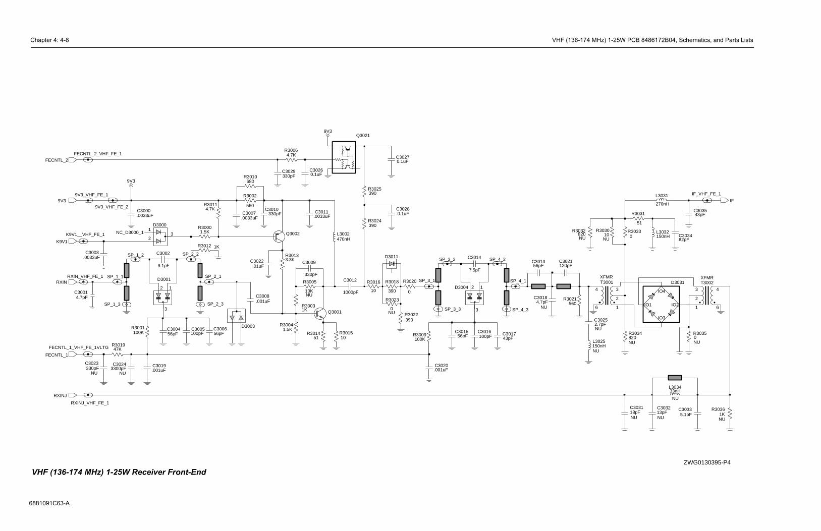
Chapter 4: 4-8 VHF (136-174 MHz) 1-25W PCB 8486172B04, Schematics, and Parts Lists
6881091
43pFC3035
FE
120pFC3021
56pFC3013
C301743pF
150nHL3032
NU4.7pF
C3018
NU820
R3032
IF_VHF_FE_1
2.7pFNU
270nH
C3025
L3031
5.1pFC3033
IO1 IO2
IO3
IO4
D3031
4
6
3
1
2
XFMRT3001
NU0R3035
R30330
SP_4_1
C3032
NU13pF
XFMRT3002
4
6
3
1
2
NU
33nHL3034
51
R3031
R3021560
SP_4_3
R3034
NU820
_2
10NU
R3030
L3025150nHNU
F
R3036
NU1K
82pFC3034
18pFC3031
NU
IF
FE
VHF (ZWG0130395-P4
C63-A
56pFC3006
Q3001
NU330pFC3023
47KR3019
RXINJ_VHF_FE_1
9.1pF
CNTL_2
C3015
C3002
56pF
.0033uFC3011
9V3
C30014.7pF
Q3002
R3010680
1000pF
C3012
R3002
560
FECNTL_2_VHF_FE_1
SP_2_3
SP_2_1
SP_2_2
100KR3001
470nHL3002
56pFC3004
RXIN_VHF_FE_1
9V3_VHF_FE_1
R30041.5K
D3003
.0033uFC3000
R3014
12
3
51
C3005
D3001
100pF10
R3015
.001uFC3008
1
23
SP_4
D3000
SP_3_3
100KR3009
9V3_VHF_FE_2
R3003
C3020
1K
.001uF
100pFC3016
R30001.5K
C3024
NU3300pF
R3023
0NU
390R3024
0
SP_1_3
R3020
390
R3018
R3022390
C3014
10
7.5pF
SP_1_2
R3016
R3012 1K
D3011
C30270.1uF
C30260.1uF
Q3021
RXIN
K9V1__VHF_FE_1
.0033uFC3007
ECNTL_1_VHF_FE_1VLTG
.001uFC3019
4.7KR3006
C30280.1uF
390R3025
3.3KR3013
SP_3_2.0033uFC3003
4.7KR3011
330pF
C3009
R3005
NU10K
330pFC3010
SP_1_1
.01uFC3022
12
3
D3004
RXINJ
CNTL_1
SP_3_1
C3029
K9V1
9V3330pF
NC_D3000_1
9V3
136-174 MHz) 1-25W Receiver Front-End

VHF (136-174 MHz) 1-25W PCB 8486172B04, Schematics, and Parts Lists Chapter 4: 4-9
6881091C63-A
CFUCJ455FNU
GND
3
IN1 OUT 2
FL3113
10K
R3152
QU
AD
IN
10
IFA
MP
_DE
C1
19
IFA
MP
_DE
C2
17
LIM
_DE
C1
LIM
_DE
C2
12
GN
D 15
IFA
MP
IN
18
IFA
MP
OU
T
16
Q3152
C31390.1uF C3141
0.1uF
RSSI_VHF_IF_1
14
VDD
7
VSS
U3115-4MC74HC4066
12
CNTL
11 10
C3143120pF
C31400.1uF
C31440.1uF
1.2K Y310245B01455KHz2
1R3135
S
7
C31420.1uF
74HC4066
9D
DISCAUDIO_VHF_IF_1
U3111-3
CFUCJ455D
GND
3
IN1 OUT 2
RSSI
FL3114
C3152.01uF
.01uFC3151
R315310K
14
VDD
7
VSS
U3115-1MC74HC4066
13
CNTL
12
0.1uFC31453.3K
R3145
BWSELECT_VHF_IF_1
DISCAUDIO
3
GN
D1
GN
D2
4
1 IN 2OUT
BWSELECT
CFWC455FFL3115
74HC4066
10D
7
S
5
43 VDD
14
VSS
7
U3111-4
U3115-2MC74HC4066
CNTL
C31470.1uF
C31464700pF
R31442.4K
C3155.01uF
Q3155NU
10K
R3155
R3151
1.2KNU
10KR3154
R3147
12K
Q3151
CNTL
6
8 9VDD
14
VSS
7
U3115-3MC74HC4066
680
R3146
9V3
9V3
9V3
FIC
12.5kHz 0VDC20/25kHz 5VDC
VHF (136-174 MHz) 1-25W IF
ZWG0130396-P4
C313630pF
R310210
C31139.1pFNU
100NU
100
R3104
R3105
R3107
6.8K
OS
CO
UT
3
RF
IN
1
RF
IN_D
EC
2
RS
SIO
UT
5
RS
SI_
FE
ED
9
VC
C6
LIM
IN
14
LIM
OU
T
1113
MIX
OU
T
20
OS
CIN
4
AU
DIO
OU
T
8
AU
DIO
_FE
ED
7
U3101
18pFC3114
0.1u
FC
3134
OUT 2
FL3112CFWC455D
GN
D1
3 4
GN
D2
IN1
33pF
C3135
R3115
GN
D2
2G
ND
34 5
GN
D4
3IN 6OUT
390
12R17FL3102
1G
ND
1
GN
D1
1 2G
ND
24
GN
D3
GN
D4
5
IN3
OUT6
R3117
12R1612R16FL3101
27K
Q3102
R31338.2K
R3134
10K
10R3112
5V
C3115
620nH
22pF
L3100
VS
MC
CNTL
6
8 VD
14
Q3101
.039uFC3137
C3104
0.1uF
D3101
C3122
.039uF
9V3
C31110.1uF
R3114
NU100
1pFNU
C3131
L3101620nH
2.2pF
CFWC455G
GN
D1
3 4
GN
D2
IN1 OUT 2
C3101
FL3111
C3103
33pF
C313310uFC3132
0.1uF
MC
12
CNTL
11
14
VD
VS
C31382.2uF
15KR3132
C3123.039uF
6.8K
R3118
12KR3111
5V_VHF_IF_1
R3130
13
CNTL
12
14
VDD
7
VSS
51
VDD
14
VSS
7
U3111-1
MC74HC4066
MC74HC4066
MC74HC4066
CNTL
5
43
U3111-2
R310627K
GND2
GND1
4
OUT3
IN1
Y310112R17
44.395MHz
9V3_VHF_IF_2
IFIN_VHF_IF_1
IF
0.1uF
C3116
330R3116
L3112
9V3_VHF_IF_1
620nH
620nH
620
L3111
C3121R3108
0.1uF
C3110
27pF
12KR3101
15pFC3102
82pF
9V3
C3112
5V
5V
9V3
9V3
5V
9V3
I
C3100
18pF
1KR3113
NU
3.9VDC
3VDC
0.75VDC0.75VDC
3VDC
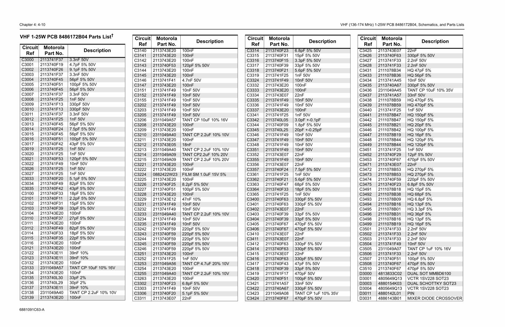
Chapter 4: 4-10 VHF (136-174 MHz) 1-25W PCB 8486172B04, Schematics, and Parts Lists
688109
VHF 1 †
CircRe
C300C300C300C300C300C300C300C300C300C300C301C3011C301C301C301C301C301C301C301C302C302C302C302C302C303C303C303C310C310C310C310C310C3110C3111C3112C3114C3115C3116C312C312C312C313C313C313C313C313C313C313C313
% 50V% 50V% 50V
% 50V% 50V
V0V
0V0V
V-0.1pF% 50V-0.25pF0V0V0V0V
0V
% 50VV% 50V
% 50V% 50VV5% 50V5% 50V
% 50V% 50V5% 50V5% 50V
5% 50V5% 50V
5% 50V% 50V% 50V50V5% 50V0V5% 50VP 1uF 10% 35V
5% 50V
Description
C3425 2113743E07 22nFC3426 2113740F63 330pF 5% 50VC3427 2113741F33 2.2nF 50VC3428 2113741F33 2.2nF 50VC3431 2111078B34 HQ 47pF 5%C3433 2111078B36 HQ 56pF 5%C3434 2113741A45 10nF 50VC3435 2113740A67 330pF 5% 50VC3436 2311049A45 TANT CP 10uF 10% 35VC3437 2113741A57 33nF 50VC3438 2111078B59 HQ 470pF 5%C3439 2111078B59 HQ 470pF 5%C3440 2113741F25 1nF 50VC3441 2111078B47 HQ 150pF 5%C3442 2111078B47 HQ 150pF 5%C3445 2111078B21 HQ 20pF 5%C3446 2111078B42 HQ 100pF 5%C3447 2111078B19 HQ 16pF 5%C3448 2111078B44 HQ 120pF 5%C3449 2111078B44 HQ 120pF 5%C3451 2113741F25 1nF 50VC3452 2113740F29 12pF 5% 50VC3453 2113740F67 470pF 5% 50VC3471 2113743E07 22nFC3472 2111078B53 HQ 270pF 5%C3473 2111078B53 HQ 270pF 5%C3474 2113740F59 220pF 5% 50VC3475 2113740F23 6.8pF 5% 50VC3491 2111078B18 HQ 15pF 5%C3492 2111078B38 HQ 68pF 5%C3493 2111078B09 HQ 6.8pF 5%C3494 2111078B16 HQ 13pF 5%C3495 2111078B01 HQ 3.3pF 5%C3496 2111078B31 HQ 36pF 5%C3498 2111078B16 HQ 13pF 5%C3499 2111078B19 HQ 16pF 5%C3501 2113741F33 2.2nF 50VC3502 2113741F33 2.2nF 50VC3503 2113741F33 2.2nF 50VC3504 2113741F49 10nF 50VC3505 2311049A07 TANT CP 1uF 10% 16VC3506 2113741F33 2.2nF 50VC3507 2113740F51 100pF 5% 50VC3508 2113740F67 470pF 5% 50VC3510 2113740F67 470pF 5% 50VD3000 4813833C02 DUAL SOT MMBD6100D3001 4805649Q13 VCTR 1SV228 SOT23D3003 4880154K03 DUAL SCHOTTKY SOT23D3004 4805649Q13 VCTR 1SV228 SOT23D3011 4880142L01 PIND3031 4886143B01 MIXER DIODE CROSSOVER
Circuit Ref
Motorola Part No. Description
1C63-A
-25W PCB 8486172B04 Parts List
uit f
Motorola Part No. Description
0 2113741F37 3.3nF 50V1 2113740F19 4.7pF 5% 50V2 2113740F26 9.1pF 5% 50V3 2113741F37 3.3nF 50V4 2113740F45 56pF 5% 50V5 2113740F51 100pF 5% 50V6 2113740F45 56pF 5% 50V7 2113741F37 3.3nF 50V8 2113741F25 1nF 50V9 2113741F13 330pF 50V0 2113741F13 330pF 50V
2113741F37 3.3nF 50V2 2113741F25 1nF 50V3 2113740F45 56pF 5% 50V4 2113740F24 7.5pF 5% 50V5 2113740F45 56pF 5% 50V6 2113740F51 100pF 5% 50V7 2113740F42 43pF 5% 50V9 2113741F25 1nF 50V0 2113741F25 1nF 50V1 2113740F53 120pF 5% 50V2 2113741F49 10nF 50V6 2113741F25 1nF 50V7 2113741F25 1nF 50V3 2113740F20 5.1pF 5% 50V4 2113740F49 82pF 5% 50V5 2113740F42 43pF 5% 50V0 2113740F33 18pF 5% 50V1 2113740F11 2.2pF 5% 50V2 2113740F31 15pF 5% 50V3 2113740F39 33pF 5% 50V4 2113743E20 100nF
2113740F37 27pF 5% 50V2113743E20 100nF2113740F49 82pF 5% 50V2113740F33 18pF 5% 50V2113740F35 22pF 5% 50V2113743E20 100nF
1 2113743E20 100nF2 2113743E11 39nF 10%3 2113743E11 39nF 10%2 2113743E20 100nF3 2311049A57 TANT CP 10uF 10% 16V4 2113743E20 100nF5 2113740L30 33pF 2%6 2113740L29 30pF 2%7 2113743E11 39nF 10%8 2311049A40 TANT CP 2.2uF 10% 10V9 2113743E20 100nF
C3140 2113743E20 100nFC3141 2113743E20 100nFC3142 2113743E20 100nFC3143 2113740F53 120pF 5% 50VC3144 2113743E20 100nFC3145 2113743E20 100nFC3146 2113741F41 4.7nF 50VC3147 2113743E20 100nFC3151 2113741F49 10nF 50VC3152 2113741F49 10nF 50VC3155 2113741F49 10nF 50VC3202 2113741F49 10nF 50VC3203 2113741F49 10nF 50VC3205 2113741F49 10nF 50VC3206 2311049A57 TANT CP 10uF 10% 16VC3208 2113743E20 100nFC3209 2113743E20 100nFC3210 2311049A40 TANT CP 2.2uF 10% 10VC3211 2113743E20 100nFC3212 2113743E05 18nFC3213 2311049A40 TANT CP 2.2uF 10% 10VC3214 2311049A09 TANT CP2.2uF 10% 20VC3215 2311049A09 TANT CP 2.2uF 10% 20VC3221 2113743E20 100nFC3222 2113743E20 100nFC3224 0882422W23 FILM SM 1.0uF 15V 5%C3225 2113743E20 100nFC3226 2113740F25 8.2pF 5% 50VC3227 2113740F51 100pF 5% 50VC3228 2113743E20 100nFC3229 2113743E12 47nF 10%C3231 2113741F49 10nF 50VC3232 2113741F49 10nF 50VC3233 2311049A40 TANT CP 2.2uF 10% 10VC3234 2113741F49 10nF 50VC3235 2113741F49 10nF 50VC3242 2113740F59 220pF 5% 50VC3243 2113740F59 220pF 5% 50VC3244 2113740F59 220pF 5% 50VC3245 2113740F59 220pF 5% 50VC3246 2113740F59 220pF 5% 50VC3251 2113743E20 100nFC3252 2113741F25 1nF 50VC3253 2311049A56 TANT CP 4.7uF 20% 10VC3254 2113743E20 100nFC3255 2311049A40 TANT CP 2.2uF 10% 10VC3263 2113743E20 100nFC3302 2113740F23 6.8pF 5% 50VC3303 2113741F49 10nF 50VC3306 2113740F20 5.1pF 5% 50VC3311 2113743E07 22nF
Circuit Ref
Motorola Part No. Description
C3314 2113740F23 6.8pF 5C3315 2113740F31 15pF 5C3316 2113740F15 3.3pF 5C3317 2113740F39 33pF 5C3318 2113740F21 5.6pF 5C3319 2113741F25 1nF 50C3324 2113741F49 10nF 5C3332 2113743E20 100nFC3333 2113743E20 100nFC3334 2113743E07 22nFC3335 2113741F49 10nF 5C3336 2113741F49 10nF 5C3337 2113743E20 100nFC3341 2113741F25 1nF 50C3342 2113740L05 3.0pF +C3344 2113740F09 1.8pF 5C3345 2113740L25 20pF +C3346 2113741F49 10nF 5C3347 2113741F49 10nF 5C3348 2113741F49 10nF 5C3351 2113741F49 10nF 5C3352 2113743E07 22nFC3355 2113741F49 10nF 5C3356 2113743E07 22nFC3357 2113740F24 7.5pF 5C3361 2113741F25 1nF 50C3362 2113740F21 5.6pF 5C3363 2113740F47 68pF 5C3364 2113740F33 18pF 5C3365 2113741F25 1nF 50C3400 2113740F63 330pF C3401 2113740F63 330pF C3402 2113743E07 22nFC3403 2113740F39 33pF 5C3404 2113740F39 33pF 5C3405 2113740F67 470pF C3406 2113740F67 470pF C3410 2113743E07 22nFC3411 2113743E07 22nFC3412 2113740F63 330pF C3414 2113740F63 330pF C3415 2113743E07 22nFC3416 2113740F63 330pF C3417 2113740F43 47pF 5C3418 2113740F39 33pF 5C3419 2113741F17 470pF C3420 2113740F51 100pF C3421 2113741A57 33nF 5C3422 2113740A67 330pF C3423 2311049A08 TANT CC3424 2113740F67 470pF
Circuit Ref
Motorola Part No.
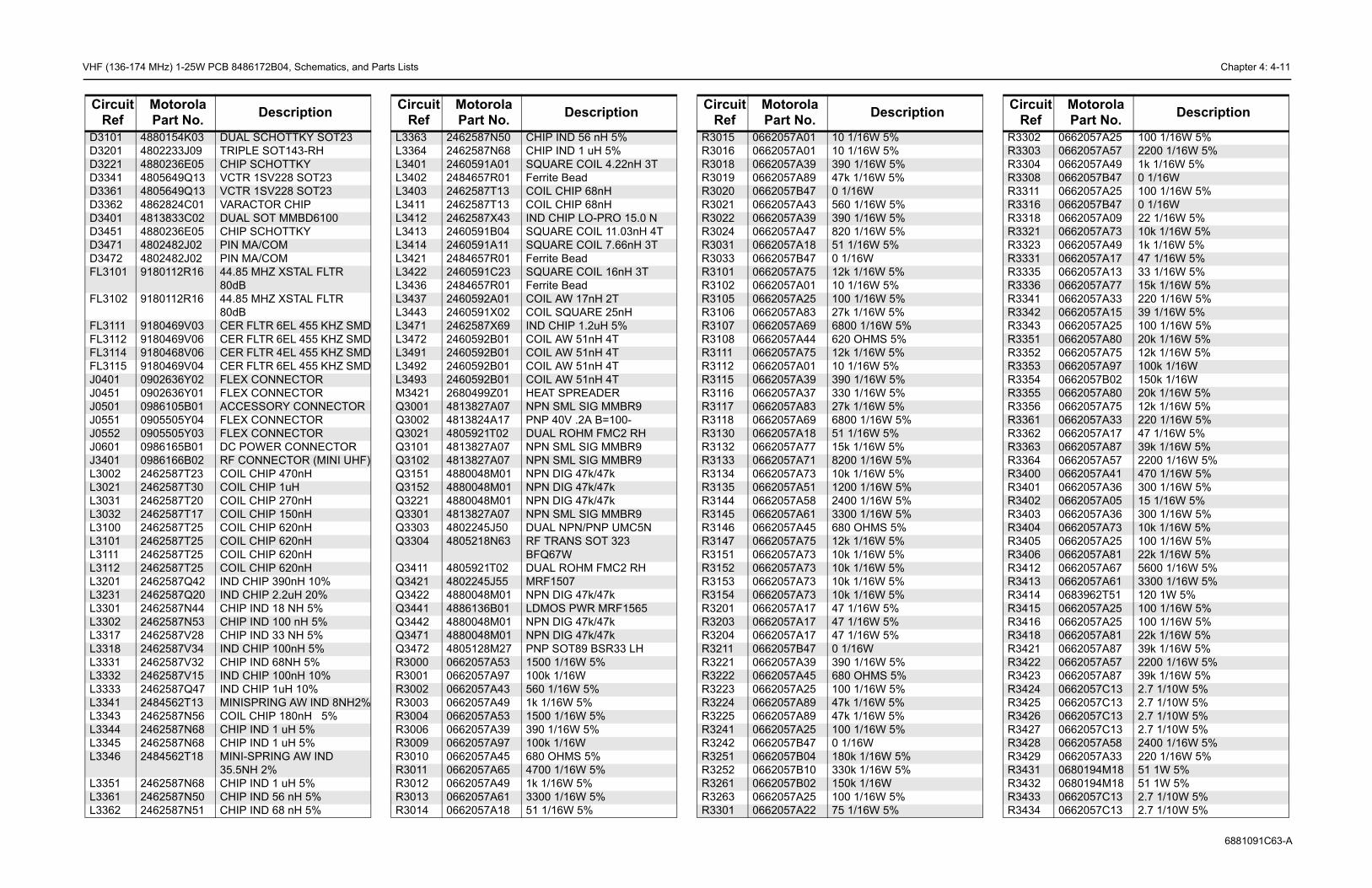
V Chapter 4: 4-11
6881091C63-A
0 1/16W 5%0 1/16W 5%90 1/16W 5%7k 1/16W 5% 1/16W60 1/16W 5%90 1/16W 5%20 1/16W 5%1 1/16W 5% 1/16W2k 1/16W 5%0 1/16W 5%00 1/16W 5%7k 1/16W 5%800 1/16W 5%20 OHMS 5%2k 1/16W 5%0 1/16W 5%90 1/16W 5%30 1/16W 5%7k 1/16W 5%800 1/16W 5%1 1/16W 5%5k 1/16W 5%200 1/16W 5%0k 1/16W 5%200 1/16W 5%400 1/16W 5%300 1/16W 5%80 OHMS 5%2k 1/16W 5%0k 1/16W 5%0k 1/16W 5%0k 1/16W 5%0k 1/16W 5%7 1/16W 5%7 1/16W 5%7 1/16W 5% 1/16W90 1/16W 5%80 OHMS 5%00 1/16W 5%7k 1/16W 5%7k 1/16W 5%00 1/16W 5% 1/16W80k 1/16W 5%30k 1/16W 5%50k 1/16W00 1/16W 5%5 1/16W 5%
Description
R3302 0662057A25 100 1/16W 5%R3303 0662057A57 2200 1/16W 5%R3304 0662057A49 1k 1/16W 5%R3308 0662057B47 0 1/16WR3311 0662057A25 100 1/16W 5%R3316 0662057B47 0 1/16WR3318 0662057A09 22 1/16W 5%R3321 0662057A73 10k 1/16W 5%R3323 0662057A49 1k 1/16W 5%R3331 0662057A17 47 1/16W 5%R3335 0662057A13 33 1/16W 5%R3336 0662057A77 15k 1/16W 5%R3341 0662057A33 220 1/16W 5%R3342 0662057A15 39 1/16W 5%R3343 0662057A25 100 1/16W 5%R3351 0662057A80 20k 1/16W 5%R3352 0662057A75 12k 1/16W 5%R3353 0662057A97 100k 1/16WR3354 0662057B02 150k 1/16WR3355 0662057A80 20k 1/16W 5%R3356 0662057A75 12k 1/16W 5%R3361 0662057A33 220 1/16W 5%R3362 0662057A17 47 1/16W 5%R3363 0662057A87 39k 1/16W 5%R3364 0662057A57 2200 1/16W 5%R3400 0662057A41 470 1/16W 5%R3401 0662057A36 300 1/16W 5%R3402 0662057A05 15 1/16W 5%R3403 0662057A36 300 1/16W 5%R3404 0662057A73 10k 1/16W 5%R3405 0662057A25 100 1/16W 5%R3406 0662057A81 22k 1/16W 5%R3412 0662057A67 5600 1/16W 5%R3413 0662057A61 3300 1/16W 5%R3414 0683962T51 120 1W 5%R3415 0662057A25 100 1/16W 5%R3416 0662057A25 100 1/16W 5%R3418 0662057A81 22k 1/16W 5%R3421 0662057A87 39k 1/16W 5%R3422 0662057A57 2200 1/16W 5%R3423 0662057A87 39k 1/16W 5%R3424 0662057C13 2.7 1/10W 5%R3425 0662057C13 2.7 1/10W 5%R3426 0662057C13 2.7 1/10W 5%R3427 0662057C13 2.7 1/10W 5%R3428 0662057A58 2400 1/16W 5%R3429 0662057A33 220 1/16W 5%R3431 0680194M18 51 1W 5%R3432 0680194M18 51 1W 5%R3433 0662057C13 2.7 1/10W 5%R3434 0662057C13 2.7 1/10W 5%
Circuit Ref
Motorola Part No. Description
HF (136-174 MHz) 1-25W PCB 8486172B04, Schematics, and Parts Lists
D3101 4880154K03 DUAL SCHOTTKY SOT23D3201 4802233J09 TRIPLE SOT143-RHD3221 4880236E05 CHIP SCHOTTKYD3341 4805649Q13 VCTR 1SV228 SOT23D3361 4805649Q13 VCTR 1SV228 SOT23D3362 4862824C01 VARACTOR CHIPD3401 4813833C02 DUAL SOT MMBD6100D3451 4880236E05 CHIP SCHOTTKYD3471 4802482J02 PIN MA/COMD3472 4802482J02 PIN MA/COMFL3101 9180112R16 44.85 MHZ XSTAL FLTR
80dBFL3102 9180112R16 44.85 MHZ XSTAL FLTR
80dBFL3111 9180469V03 CER FLTR 6EL 455 KHZ SMDFL3112 9180469V06 CER FLTR 6EL 455 KHZ SMDFL3114 9180468V06 CER FLTR 4EL 455 KHZ SMDFL3115 9180469V04 CER FLTR 6EL 455 KHZ SMDJ0401 0902636Y02 FLEX CONNECTORJ0451 0902636Y01 FLEX CONNECTORJ0501 0986105B01 ACCESSORY CONNECTORJ0551 0905505Y04 FLEX CONNECTORJ0552 0905505Y03 FLEX CONNECTORJ0601 0986165B01 DC POWER CONNECTORJ3401 0986166B02 RF CONNECTOR (MINI UHF)L3002 2462587T23 COIL CHIP 470nHL3021 2462587T30 COIL CHIP 1uHL3031 2462587T20 COIL CHIP 270nHL3032 2462587T17 COIL CHIP 150nHL3100 2462587T25 COIL CHIP 620nHL3101 2462587T25 COIL CHIP 620nHL3111 2462587T25 COIL CHIP 620nHL3112 2462587T25 COIL CHIP 620nHL3201 2462587Q42 IND CHIP 390nH 10%L3231 2462587Q20 IND CHIP 2.2uH 20%L3301 2462587N44 CHIP IND 18 NH 5%L3302 2462587N53 CHIP IND 100 nH 5%L3317 2462587V28 CHIP IND 33 NH 5%L3318 2462587V34 IND CHIP 100nH 5%L3331 2462587V32 CHIP IND 68NH 5%L3332 2462587V15 IND CHIP 100nH 10%L3333 2462587Q47 IND CHIP 1uH 10%L3341 2484562T13 MINISPRING AW IND 8NH2%L3343 2462587N56 COIL CHIP 180nH 5%L3344 2462587N68 CHIP IND 1 uH 5%L3345 2462587N68 CHIP IND 1 uH 5%L3346 2484562T18 MINI-SPRING AW IND
35.5NH 2%L3351 2462587N68 CHIP IND 1 uH 5%L3361 2462587N50 CHIP IND 56 nH 5%L3362 2462587N51 CHIP IND 68 nH 5%
Circuit Ref
Motorola Part No. Description
L3363 2462587N50 CHIP IND 56 nH 5%L3364 2462587N68 CHIP IND 1 uH 5%L3401 2460591A01 SQUARE COIL 4.22nH 3TL3402 2484657R01 Ferrite BeadL3403 2462587T13 COIL CHIP 68nHL3411 2462587T13 COIL CHIP 68nHL3412 2462587X43 IND CHIP LO-PRO 15.0 NL3413 2460591B04 SQUARE COIL 11.03nH 4TL3414 2460591A11 SQUARE COIL 7.66nH 3TL3421 2484657R01 Ferrite BeadL3422 2460591C23 SQUARE COIL 16nH 3TL3436 2484657R01 Ferrite BeadL3437 2460592A01 COIL AW 17nH 2TL3443 2460591X02 COIL SQUARE 25nHL3471 2462587X69 IND CHIP 1.2uH 5%L3472 2460592B01 COIL AW 51nH 4TL3491 2460592B01 COIL AW 51nH 4TL3492 2460592B01 COIL AW 51nH 4TL3493 2460592B01 COIL AW 51nH 4TM3421 2680499Z01 HEAT SPREADERQ3001 4813827A07 NPN SML SIG MMBR9Q3002 4813824A17 PNP 40V .2A B=100-Q3021 4805921T02 DUAL ROHM FMC2 RHQ3101 4813827A07 NPN SML SIG MMBR9Q3102 4813827A07 NPN SML SIG MMBR9Q3151 4880048M01 NPN DIG 47k/47kQ3152 4880048M01 NPN DIG 47k/47kQ3221 4880048M01 NPN DIG 47k/47kQ3301 4813827A07 NPN SML SIG MMBR9Q3303 4802245J50 DUAL NPN/PNP UMC5NQ3304 4805218N63 RF TRANS SOT 323
BFQ67WQ3411 4805921T02 DUAL ROHM FMC2 RHQ3421 4802245J55 MRF1507Q3422 4880048M01 NPN DIG 47k/47kQ3441 4886136B01 LDMOS PWR MRF1565Q3442 4880048M01 NPN DIG 47k/47kQ3471 4880048M01 NPN DIG 47k/47kQ3472 4805128M27 PNP SOT89 BSR33 LHR3000 0662057A53 1500 1/16W 5%R3001 0662057A97 100k 1/16WR3002 0662057A43 560 1/16W 5%R3003 0662057A49 1k 1/16W 5%R3004 0662057A53 1500 1/16W 5%R3006 0662057A39 390 1/16W 5%R3009 0662057A97 100k 1/16WR3010 0662057A45 680 OHMS 5%R3011 0662057A65 4700 1/16W 5%R3012 0662057A49 1k 1/16W 5%R3013 0662057A61 3300 1/16W 5%R3014 0662057A18 51 1/16W 5%
Circuit Ref
Motorola Part No. Description
R3015 0662057A01 1R3016 0662057A01 1R3018 0662057A39 3R3019 0662057A89 4R3020 0662057B47 0R3021 0662057A43 5R3022 0662057A39 3R3024 0662057A47 8R3031 0662057A18 5R3033 0662057B47 0R3101 0662057A75 1R3102 0662057A01 1R3105 0662057A25 1R3106 0662057A83 2R3107 0662057A69 6R3108 0662057A44 6R3111 0662057A75 1R3112 0662057A01 1R3115 0662057A39 3R3116 0662057A37 3R3117 0662057A83 2R3118 0662057A69 6R3130 0662057A18 5R3132 0662057A77 1R3133 0662057A71 8R3134 0662057A73 1R3135 0662057A51 1R3144 0662057A58 2R3145 0662057A61 3R3146 0662057A45 6R3147 0662057A75 1R3151 0662057A73 1R3152 0662057A73 1R3153 0662057A73 1R3154 0662057A73 1R3201 0662057A17 4R3203 0662057A17 4R3204 0662057A17 4R3211 0662057B47 0R3221 0662057A39 3R3222 0662057A45 6R3223 0662057A25 1R3224 0662057A89 4R3225 0662057A89 4R3241 0662057A25 1R3242 0662057B47 0R3251 0662057B04 1R3252 0662057B10 3R3261 0662057B02 1R3263 0662057A25 1R3301 0662057A22 7
Circuit Ref
Motorola Part No.

Chapter 4: 4-12 VHF (136-174 MHz) 1-25W PCB 8486172B04, Schematics, and Parts Lists
688109
R343R344R344R344R344R344R344R345R345R345R345R347R347R347R347R349R350R350R350R350R350R350R350T3001T3002U310U3111
U3115
U320
U3211U330U340U340U350U350Y3101Y3102
Y3263
* Y32
CircRe
1C63-A
* Motorola Depot Servicing onlyReference designators with an asterisk indicate components which are not field-replaceable because they need to be calibrated with specialized factory equipment after installation. Radios in which these parts have been replaced in the field will be off frequency at temperature extremes.
† Replacement boards must be ordered from CCSD (formerly AAD) using the number shown in the model charts in Section 1. Boards are not orderable using the 84-prefixed number.
5 0662057C13 2.7 1/10W 5%1 0662057A87 39k 1/16W 5%2 0662057A57 2200 1/16W 5%3 0662057A87 39k 1/16W 5%4 0662057C19 4.7 1/10W 5%5 0662057A58 2400 1/16W 5%6 0662057B47 0 1/16W2 0662057A65 4700 1/16W 5%4 0662057A73 10k 1/16W 5%5 0662057A97 100k 1/16W7 0683962T51 120 1W 5%1 0662057A41 470 1/16W 5%3 0680194M18 51 1W 5%4 0680194M18 51 1W 5%5 0662057A73 10k 1/16W 5%1 0662057A73 10k 1/16W 5%1 0662057A69 6800 1/16W 5%2 0662057A87 39k 1/16W 5%4 0662057A73 10k 1/16W 5%5 0662057A97 100k 1/16W7 0662057A80 20k 1/16W 5%8 0662057A97 100k 1/16W9 0662057A49 1k 1/16W 5%
2508396X02 TRANSFORMER2508397X02 TRANSFORMER
1 5186144B01 FM IF IC SA6165113805A86 IC QUAD ANALOG MUX/
DEMUX5113805A86 IC QUAD ANALOG MUX/
DEMUX1 5185963A27 IC TESTED AT25016 48 PIN
GFP5185963A33 VLTG REG LP2951 SO8
1 5105750U54 VCO BUFFER PKG DIE1 5105109Z67 LDMOS DRIVER VHF/UHF2 5113818A03 IC HIGH PERFORMANCE SI1 5185765B01 IC POWER CONTROL2 5185963A15 TEMP SENSOR 1M5
4880606B09 CRYSTAL 44.395 MHZ9186145B02 44.85 MHZ XSTAL FLTR
60dB4886182B01 VCTCXO 16.8MHz 2ppm
TTSO5V61 Not Used 16.8MHz 75Z04
uit f
Motorola Part No. Description
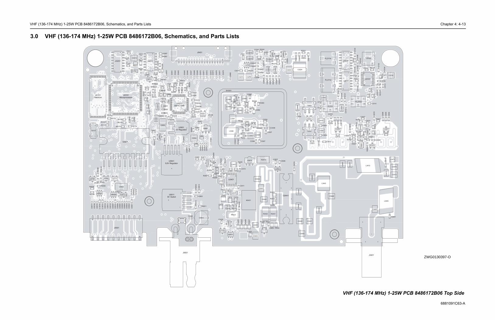
VHF (136-174 MHz) 1-25W PCB 8486172B06, Schematics, and Parts Lists Chapter 4: 4-13
6881091C63-A
3
ZWG0130397-O
C3002
C3
00
4
C3
00
5
C3
00
6
C3007
C3008
C3
00
9
C3010
C3011
C3
01
2
C3013
C3014
C3
01
5
C3
01
6
C3
01
7
C3
01
8
C3
01
9
C3020
C3021
C3027C3028C3034
C3100
C3101
C3
10
2
C3
10
3
C3114
C3
11
5
C3
13
1
C3
13
2
C3133
C3
13
4
C3135
C3136
C3
13
7
C3
13
9
C3140
C3141
C3
14
2
C3143
C3
14
5
C3
14
8
C3
22
1
4
C34412
443
C3
44
4
C3
44
5
C3446
C3
44
7
C3472
C3473
C3
47
4
C3497
D3001
D3003
D3004
D3031
D3
47
1
D3
47
2
23
45
6
FL3101
23
45
6
FL3102
4
3 2
FL3112
FL3114
2 3
J3401
L3
00
2
L3031
L3032
L3100
L31
01
L3443
L3471
L3472
L3493
Q3
00
1
Q3
02
1
R3001R3002
R3003
R3
00
4
R3009
R3013
R3
01
4R
30
15
R3
01
6
R3024
R3025R3026
R3027
R3028
R3031
R3
10
1
R3
10
6
R3
111
R3
11
7
R3
13
0
R3
13
2
R3135
R3
14
2
R3
14
4R
31
45
R3221
R3223
R3491
3
4 6
12
T3001
3
46
1 2
T3002
11
120
10
U3101
8 7
114
U3111
8 7
114
U31152
Y3102
1
1
1
1
1
45
ZW
G0130397-O
VHF (136-174 MHz) 1-25W PCB 8486172B06 Top Side
.0 VHF (136-174 MHz) 1-25W PCB 8486172B06, Schematics, and Parts Lists
C0
10
1
C0
10
2
C0
10
4C
01
06
C0
10
7
C0131
C0132
C0211
C0212
C0
22
1
C0
22
2
C0223
C0
22
4
C0225
C0226
C0227
C0
22
8
C0
23
1
C0232
C0233
C0234
C0235
C0236
C0
23
7
C0241
C0242
C0243
C0244
C0245
C0246
C0251
C0252
C0253
C0
26
1
C0262
C0267
C0
42
1
C0
44
1
C0
44
2
C0
44
3
C0
44
5
C0
44
6
C0
44
7
C0
44
8
C0
44
9
C0
47
0
C0
47
1
C0
47
2
C0
47
3
C0
47
4
C0
47
6
C0
47
7
C0
47
8
C0
48
2
C0
48
3
C0484
C0
48
6
C0
48
7
C0
48
8
C0
49
0
C0
49
3
C0
49
4
C0
49
5
C0496
C0
50
1
C0
50
2
C0
50
3
C0
50
4
C0
50
5
C0
50
6
C0
50
8
C0
50
9
C0
51
0
C0
511
C0
51
2
C 0
51
3
C0
51
4
C0
51
5
C 0
51
6
C0
51
7
C0
51
8
C0542
C0601
C0603
C0
61
2
C0
65
1
C0652
C0654
C0
65
5
C0681
C3032
C3210
C3211
C3213
C3214C3215
C3
22
2
C3223 C322
C3226
C3227
C3
22
9
C3
23
1
C3
23
2
C3
23
3C
32
34
C3240
C3242
C3243
C3244
C3245
C3246
C3
25
2
C3
25
3C
32
54
C3255
C3324
C3336
C3337
C3341
C3
34
2
C3344
C3345
C3346 C3347
C3357 C3361
C3362C3363
C3364
C3365
C3400
C3401C3403C3404
C3410
C3411C3412
C3417C3418
C3419
C3420
C3422
C3423
C3
42
4
C3425
C3426
C3428
C3431
C3432
C3433
C3434C3435
C344
C3
C3
44
8C
34
49
C3
45
3
C3507C3508
C3509
D0201
D0
65
1
D3
22
1
D3
34
1
D3
36
1
D3362
D3401
181
J0451
2011
10
J0501
J0601
L0481
L0482
L3
03
4
L3201
L3232
L3333
L3341
L3343L3344
L3346
L3361
L3362
L3363
L3364
L3401
L3403
L3411
L3412
L3413
L3414
L3422
M3421
Q0110
Q0177Q0181Q0185
Q0681
Q3
22
1
Q3304
Q3411
Q3422
2
3
4
5
6
7
8
Q3441
Q3
44
2
Q3
47
1
Q3472
R0
10
1
R0102
R0
10
4
R0105
R0106
R0
10
8
R0110
R0114
R0115
R0116
R0131
R0132
R0170
R0181
R0
18
2
R0185
R0
18
6
R0211
R0212
R0220
R0221
R0222
R0
22
3
R0
22
4
R0225
R0226
R0227
R0
22
8 R0229
R0241
R0242
R0251
R0252
R0253
R0261
R0
26
2
R0267
R0
26
8
R0
26
9
R0510
R0
53
3
R0535
R0538
R0539
R0611
R0
61
2
R0651
R0
65
2
R0681
R0
68
2
R3211
R3
22
2
R3224
R3
22
5R3227
R3242
R3
25
1
R3
25
2
R3335
R3
33
6
R3341
R3342
R3361
R3362
R3363R3364
R3400
R3401
R3
40
2
R3403
R3404
R3405
R3406
R3414
R3415
R3416
R3
42
4
R3
42
5
R3
42
6
R3
42
7
R3431R3432
R3433
R3434
R3435
R3471
R3473
R3
50
5
R3506
R3507
R3508
R3509
SH3301
TP
34
01
1
7651
26
3217
16 1
87
1 14
U0211
1 37
2513
161
8 9
U0251
9
U0271
1
6
5
1
6
5
3
2
1
U3211
1
16
8
9
U3401
U3502
VR
05
01
VR0503VR0505
VR0510
2 3
4
Y0131
1
1
100
U0101Microprocessor
U0121Flashrom
U0221ASFIC CMP
U0611B+ Switch
U06419,6V Regulator
U06515V Regulator
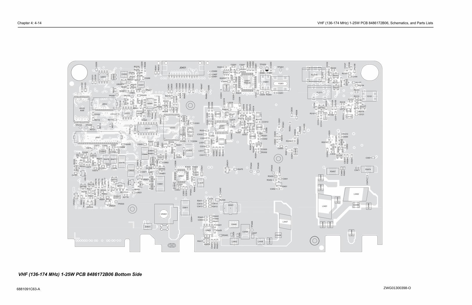
Chapter 4: 4-14 VHF (136-174 MHz) 1-25W PCB 8486172B06, Schematics, and Parts Lists
6881091
C3000
C3001
C3
02
2
C3
02
5
C3
02
6
C3
02
9
C3030
C3033
C3
03
5
C3
03
6
C3
10
4
C3
11
0 C3111
C3112
C3
11
3
C3116
C3121
C3122 C3123
C3144
C3
14
6
C3
14
7
C3
15
1C
31
52
C3
45
0 C3471
C3
47
5C3
49
1C
34
92
C3
49
3
C3
49
4
C3495
C3
49
6
C3
49
8
C3
49
9
D3000
D3
011
D3101
43
2
FL3111
FL
311
3
FL3115
L3
02
5
L3111
L3112
L3491
L3492
Q3
00
2
Q3101
Q3102
Q3
14
1
Q3151
Q3152
R3000
R3
00
6
R3010
R3
011
R3
01
2
R3018
R3
02
3
R3030
R3
03
2
R3033
3034
R3
03
5
R3
03
6
R3
10
2
R3
10
4
R3
10
5
R3107R3108
R3
11
2
R3113
R3114
R3115
R3116R3118
R3133
R3134
R3141
R3
14
6
R3147
R3
15
1
R3152
R3153
R3
15
4
R3
45
0R3457R3474
4 3
2
Y3101
1
1
43
2 1
VHF (
ZWG01300398-O
C63-AC0103
C0
10
5
C0111
C0
11
2
C0
12
1
C0
12
2
C0
12
3
C0
14
1
C0151
C0201
C0202
C0203
C0204
C0
20
5
C0254
C0
25
5
C0265
C0266
C0271C0272
C0273
C0
27
4
C0275
C0276
C0277
C0301
C0
30
2
C0303
C0
30
4
C0
30
5
C0
32
4
C0
32
5
C0331
C0
34
1
C0
34
2
C0343
C0
34
4
C0351
C0352
C0353
C0354
C0
42
2
C0
42
3
C0
42
6
C0
42
7
C0
42
8
C0
42
9
C0
43
0
C0
43
1
C0
48
5
C0491
C0492
C0497
C0
49
9
C0541
C0554
C0558
C0
55
9
C0560C0575
C0576
C0591
C0592C0593
C0611
C0621
C0622
C0641
C0644
C0645
C0661
C0662
C0
66
3
C0671
C3003
C3
02
3C
30
24
C3031
C3
20
2
C3203
C3
20
5
C3
20
6
C3
20
7
C3
20
8
C3209
C3
22
5
C3
22
8
C3235
C3241
C3251
C3
26
1
C3
26
2
C3
26
3
C3301
C3302
C3303
C3
30
4
C3
30
5
C3
30
6
C3311
C3312
C3313
C3314
C3315
C3316
C3317
C3
31
8C
33
19
C3331
C3332
C3333
C3
33
4
C3
33
5
C3
34
8
C3
35
1C
33
52
C3
35
5
C3
35
6
C3
40
2
C3
40
5
C3
40
6
C3413
C3414 C3415
C3416
C3
42
1
C3
42
7
C3436C3437
C3438
C3
43
9
C3440
C3451
C3452
C3501
C3
50
2
C3503
C3504
C3
50
5C
35
06
C3
51
0
D0101
D0151
D0179D
0301
D0
62
1
D0
66
0D
06
61
D3201 D3261
D3451
E0271E0272
E0631
12
J0401
1 40
J0551
1 18
J0552
L3
23
1
L3301
L3302
L3
311
L3317
L3318
L3331
L3332
L3
34
5
L3351
L3402
L3421
L3436
L3437
Q0
15
1
Q0171
Q0173Q0183
Q0271Q0641
Q0661
Q0662 Q0663
Q3301
Q3302
43
Q3303
12 3
Q3421
R0
10
7
R0111R0112
R0
11
3
R0
11
7
R0121
R0151
R0
15
2
R0
17
1
R0
17
2
R0173
R0174
R0
17
5
R0
17
6
R0
17
7
R0
17
8
R0
17
9
R0183
R0
18
4
R0201
R0202
R0203
R0204
R0205
R0206
R0207
R0208
R0265
R0
26
6
R0273R0274
R0275
R0
27
6
R0323
R0
32
4
R0331
R0
33
2
R0333
R0
33
5
R0
34
1
R0
34
2
R0343
R0344
R0345
R0
34
6
R0
34
7R0401
R0
40
7
R0408
R0
40
9
R0410
R0
41
2
R0
44
1
R0
46
7
R0
46
8
R0
48
1
R0482
R0511
R0
51
2
R0525
R0
52
9
R0530
R0531
R0
53
7 R0541
R0542
R0
59
1
R0592
R0621
R0641
R0642
R0
64
3
R0661
R0662R0
67
1
R0
67
2
R3
01
9
R3
02
1
R
R3201R3203
R3204
R3206
R3226
R3
22
8
R3
24
1
R3261
R3
26
2
R3263
R3301
R3302
R3303
R3
30
4
R3305
R3
30
6
R3307
R3
30
8
R3
311
R3
31
2
R3313
R3
31
4
R3
31
5
R3316
R3
31
7
R3318
R3
31
9
R3321
R3323
R3331
R3343
R3
35
1R
33
52
R3
35
3
R3
35
4
R3
35
5
R3
35
6
R3411
R3412
R3
41
3
R3417
R3418
R3421
R3
42
2
R3
42
3
R3428
R3429
R3440
R3441
R3442R3443
R3444
R3445
R3
44
6
R3452
R3
45
4
R3455
R3475
R3501
R3502R3504
S3440
TP
0101
TP0102
TP0103
TP
01
04
TP0151
TP0221
TP0222
TP0481
TP0492
TP
04
97
TP0530
TP0661
TP
3001
TP3201
TP3202
TP
34
02
TP
3403
TP
34
04
TP
34
05
TP
34
06
1 4
58
U0111
22
218
7 1
16
1 8
9
U0141
2815
14 1
U0301
U0331
1
45
8
U0341
U0342
4
5 8
U0351
14
5 8
U0652
U0
65
3
137
2513
11
1
20
10
1 4
58
U3402
1
17
9
25
U3501
VR
01
51
VR0504VR0509
VR
05
37
VR0541
VR0601
VR
06
21 VR0671
VR
34
71
6
4 3
1
Y3261
2
34
Y3263
1
1
48
U0122RAM
U3201FRACN
U3301VCOIC
1 5
136-174 MHz) 1-25W PCB 8486172B06 Bottom Side

VHF (136-174 MHz) 1-25W PCB 8486172B06, Schematics, and Parts Lists Chapter 4: 4-15
6881091C63-A
ZWG0130392-A
RXIN_VHF_PA_1
NU
NU
NUNU
NU
R3506
10K
C3443
120pF
C3444
6.2pF
C3509
width 2.032 2.216xJ3401
C3506
2200pF
R3502
39K
C3473
270pF
10KR3491
100pF
C3507
RESET_VHF_PA_1
C3504.01uF
470pF
C3503
FECNTL_2
C3502
2200pF
25nH
L3443
10K
R3504
470
R3471 Q3472
RESET
U35023
GND
POS
1
2VOUT
C3492
68pF
LM50
C34936.8pF
ATA_VHF_PA_1
20pF
C3445
1
5.6V
VR3471
2
3
C3505
1uF
6.8pF
C3475
TEMPSENSE
TEMPSENSE_CNTLR_1
1K
R3507
20K
PA_PWR_SET
R3509
C3451
1000pF
F
1
C3495
C3497
3.3pF
C3474
220pF
18
pF
R3413
3.3K
FECNTL_2_VHF_PA_1
SX_VHF_PA_1
D3472
C3446
100pF
D3451
51nH
L3493
R3474
51
R3473
51
C3491
15pF
D3471
L3471
1.2uH
51nH
R3508
100K
L3491
R3505
300K
270pF
C3472
150pF
C3496
C3442
36pF
C3510
CNTLVLTG_VHF_PA_1
470pF
PA_PWR_SET_VHF_PA_1
470pFC3453
R3501
L3492
51nH
6.8K
RXIN
13pF
C3494
20
VA
R1
18
VA
R2
24
VA
R3
VG15
6V
L19
VLIM
21
RS
31RSET
23
RX
2T
1
30TEMP
14V10
16V45
17
V5E
XT
9F168
8G
ND
1
25GND2
4IN
T
22
NA
11Q
10QX
1R
FIN
29CEX
3C
I
5C
J
7C
L
26CLK
12CQ
CQX1328
DATA
H99S-4U3501
32ANO
27BPOS
FECNTL_1_VHF_PA_1
16pF
C3447
LK_VHF_PA_1
470pF
R3452
12K
C3498
13pF
CNTLVLTG
16pF
C3499
470pF
C3450470
R3450
TP3405
10KR3475
R3457
120
51nH
L3472
12pF
C3452
K9V1
K9V1_VHF_PA_1
TP3404
FECNTL_1
9V3FLT
NC
9V3FLTA+
NC
9V3FLT 9V3FLT
MOSBIAS_1 NC
NC
NC
NCNC
NC
NC
NC
74 MHz) 1-25W Power Amplifier for PCBs 8486172B06 and 8486172B07
47K
47K
47K
47K
47K
47K
NU
NU
17nH
L3437
NU
0
R3440
C3427
56pF
39K
10K
6.8K
R3411NU
C3508
1uF
C3423
0.8x25
1.542x4
7.5
R3427
R3426
2.7
2.7
2.7R3428
R3425
2.4K
120
R3414
2.4K
MOSBIAS_2_VHF_PA_1
R3445
L3412
C3432
15nH
C3404
33pF
2200pF
C3410
.022uF
PASUPVLTG_VHF_PA_1
R3415
100
330pF
C3426
Q3421
R3417
39K
R3443
R3441
C3416
330pF
330pF
C3400 R3400
470
51R3432
.033uFC3437
L3436
57R01
470pFC3419
TP3402
TP3403
57R01
L3402
C3406
470pF
R3401300
C3428
C3435
2200pF
C3449
330pF
120pF
C3434
.01uF
MOSBIAS_2
47K
R3404
47pF
C3431
C3421
.033uF
CLK
51R3431
R34352.7
INT_SWB
C3425
.022uF
D
2.2KR3442
C3422
330pF
R3444
4.7
39K
R3421
DATA
33pF
C3403
.022u
C347
CSX
6
5
7
8
4
TXINJ_VHF_PA_1
LM2904U3402-2
470pF
9V3
C3501
2200pF
INT_SWB_VHF_PA_1
D3401
C
33pF
C3418
L3411
68nH .022uF
C3411
R3403
300
470pF
C3405
100K
R3406
11.03nH
5.6KR3412
L3413
120pF
C3448
2.7R3424
47pF
C3417
C3439
470pF
0
R3446
R3455100K
10uF
C3436
R3429
220
R3433 2.7
C3433
56pF
22K
R3418
2
3
1
8
4
C3440
1000pF
U3402-1
LM2904
TXINJ
Q3442
R3402
15
39K
R3423
Q3411
TP3406 C
TP3401
L3422
13.85nH
470pF
470pF
C3424
30K
C3438
R3454
R3405100
330pF
C3401
RFIN
16
RFOUT16
RFOUT27
VCNTRL1
VD114 2
VG1
VG23
GN
D1
4
GN
D2
5
GN
D3
12
GN
D4
13
NC18
NC29
NC310
NC415
09Z67
U3401
G211
PASUPVLTG
100
L3403
R3416
Q3422
68nH 330pF
9V3_VHF_PA_1
C3412
SWITCH
S3440
7.66nH
L3414
C3413
.022uF
C3441
150pF
R34342.7
R3422
2.2K
Q3471
57R01
L3421
330pF
C3414
D
G
GND1
GND2
S1
S2
S3
S4
Q3441
.022uF
C3415
100pF
C3420
C3402
.022uF
NC
PA_SWB
A+
L3401
4.22nH
U_DRIVER
9V3FLT
PA_SWB
U_DRIVER9V3FLT
9V3FLT
A+
U_PREDRIVER
NC
PA_SWB
9V3FLT
U_PREDRIVER
2
NU
VHF (136-1
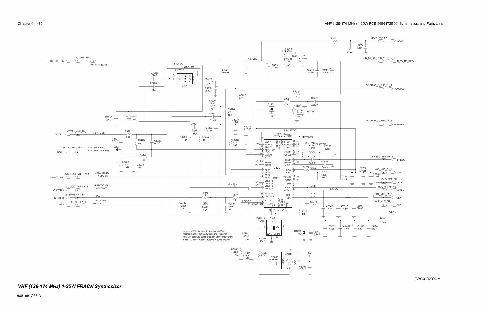
Chapter 4: 4-16 VHF (136-174 MHz) 1-25W PCB 8486172B06, Schematics, and Parts Lists
6881091
47K
47K
3.6
3V
DC
C3231.01uF
C3229
0.1uF
.047uF
CLK
C3251
VCOBIAS_2
C32268.2pF
MODIN_VHF_FN_1
R3252
VCOBIAS_1_VHF_FN_1
330K
PRESC_VHF_FN_1
VSF_VHF_FN_1
DATA
CSX_VHF_FN_1
100pF
C3227
CSX
IN_5V_RF_REG_VHF_FN_1
100KR3227
0.1uFC3254
.01uF
C3232
PRESC
C32142.2uF
C32630.1uF
76
0
1
1
2
5
8
0
79
9
2
0
VCOBIAS_1
VSF
0
R3211
L3231
0.1uF
C3211
TP32021
2.2uH
C3243220pF
VDDA
VDDA_VHF_FN_1
VCOBIAS_2_VHF_FN_1
Q3221
R3251180K
220pFC3245
C3215
3224
47K
2.2uF
1
D
5IN
3
SD
VC
C 4
MODIN
C3255
DATA_VHF_FN_1
220pFC3242
2.2uF
R326147K
2.2uFC3233
CLK_VHF_FN_1
C32521000pF
.01uFC3234
C32534.7uF
NU
IN_5V_RF_REG
D3261
C3244220pF
5V
NC
NC
NC
NC
NC
VDDA
VDDA
NC
NC
NC
5VDC
-2 to +7dBm
2.5VDC
C
3.63VDC
0VDC
5VDC
ZWG0130393-A
VHF (
C63-A
(SOURCE)
R3203
A1
5A2
4A3
K11
K22
K33
47
D3201
6
47KNU
TRBL3232
2.2uH
NU
R3228
C3225
L3201
390nH
0.1uF
C3202.01uF
100
R3223
D3221
C3207
22pF
NU
47K
R3225
TP3201
16_8MHz_VHF_FN_1R3242
0
100
R3241
VCOMOD_VHF_FN_1
22pF
NU
C3240
NU
1
GND
4
GND1
3OUT6IN
16.8MHz
75Z04
Y3261
C3208
0.1uF
NU
47K
R3226
C32210.1uF
1uF
C3224
VMULT11514 VMULT212 VMULT311 VMULT4
VR
O1
3
25
WARP
23 XTAL1
XTAL224
2SFBASE
2SFCAP
3SFIN
28SFOUT
37TEST1
38TEST2
2VBPASS
47
VC
P
3NC3
44
PD
_G
ND
PD
_V
DD
5
PREIN3
33
PR
E_
GN
D3
4P
RE
_V
DD
3PVREF
1REFSEL
45IADAPT
16INDMULT
43IOUT
LOCK4
1MODIN
41 MODOUT
1NC1
2NC2
3BIAS2
4CCOMP
9CEX8
CLK
7DATA
DG
ND
636
DV
DD
19 FREFOUT
46ADAPTSW
22
AG
ND
48AUX1
1AUX2
2AUX3
3AUX4
20
AV
DD
4BIAS1
63A27
U3201
47
R3201
C32220.1uF
16_8MHz
0.1uF
C3209C3246220pF
NU
C320610uF
5V_VHF_FN_2
33KR3206
.01uF
C32280.1uF
C3235
2.2uFC3210
VCTRL_VHF_FN_1
R3204
LOCK_VHF_FN_1
47
1uFC3223
NU
R3262
NU
BWSELECT
6.2K
R
C3213
GN
2NR
4 OUT
2.2uF
VCNTL
1
ADP3300U3211
6
ERR
Y326316.8MHz
GN
D2
OUT
3
VCTRL
5V_VHF_FN_1
.01uF
R3222
680
TRB_VHF_FN_1
C3205
C3262330pF
NU
NU
VCOMOD
C3241
56pF
R3221
390
5V
C3261
NU
LOCK
39pF
BWSELECT_VHF_FN_1
C3203
4,7k
.01uF
NC
5V
R3263
NC
NC
NC
NC
NC
In case Y3261 is used instead of Y3263,
replacement of the following parts requires
new temperature compensation of the frequency:
Y3261, U3201, R3261, R3262, C3262, D3261
13.30VDC
6.83VDC
4.52VDC (R)
+1dBm
0VDC (R)
4.95VDC (R)
2.90VDC3.42VDC
1.1-4.1VD
0VDC (T)
2.62VDC (T)
4.91VDC (T)
11.28VDC
4.97VDC
2.5-11VDC
5VDC (LOCKED)
0VDC (UNLOCKED)
136-174 MHz) 1-25W FRACN Synthesizer

VHF (136-174 MHz) 1-25W PCB 8486172B06, Schematics, and Parts Lists Chapter 4: 4-17
6881091C63-A
ZWG0130394-O
0VDC (R)
1.92VDC (T)
4.52VDC (R)
2.62VDC (T)
1.42VDC (R)
0VDC (T)
4.97VDC
(R)
T)
)
)
2.5-11VDC
4.54VDC
L3333
R335612K
VCOBIAS_2_VHF_VCO_1
1uH
D3361
9V3_VHF_VCO_2VDDA_VHF_VCO_1
35.5nH
15K
L3346
R3336
R3362
47
R3354
150K
VCOMOD_VHF_VCO_1
C336368pF
C33577.5pF
1uH
L3351
L3344
1uH
C33625.6pF
C3344
1.8pF
56nH
L3361
1uH
L3364
12KR3352
VCOMOD
VCOBIAS_1_VHF_VCO_1
VCTRL
C3347
.01uF
C33370.1uF
D3341
VCOBIAS_1
100K
R3353
C3324.01uF
VCOBIAS_2
C3345
20pF
L3362
68nH
15pF
C3364
8nHL3341
56nHL3363
.022uF
C3352
VDDA
100
R3343
VSF_VHF_VCO_1
VSF
C3342
3pF
D3362
R3341
220
3355K
NU
R3363
39K
9V3_VHF_VCO_1
9V3
VCTRL_VHF_VCO_1
C3346
C3341
.01uF
1000pF
39
R3342
9V3_VHF_VCO_3
61
C3356
.022uF
0pF
180nH
L3343
C33651000pF
R3364
47K
1uHL3345
ntrolled Oscillator for PCBs 8486172B06, 8486172B07 and 8486172B08
47
K
47
K4
7K
10
K
4.2
2V
DC
(T
)
4.52VDC (R)
0VDC (T)
4.40VDC
1.53VDC
0VDC (
0.92VDC (R
0VDC (T
0VDC (R)
0-5dBm (T)
7.44VDC (R)
9.14VDC (R)
0VDC (T)
0VDC (T)
11-14dBm (R)
-2 to 7dBm
0VDC (T)
2.18VDC (R)
0VDC (T)
1.49VDC (R)
2.5
6V
DC
(R
)
0VDC (R)
0VDC (T)
4.7
8V
DC
(R
)
2.6
6V
DC
(T
)
4.52VDC (T)
WARISMOBILE VHF_VCO
4.7
8V
DC
(R
)
4.2
7V
DC
(T
)
4.91VDC (T)
9.21VDC
3.83VDC (R)
R3335
33
220
R3361
C3331
10K
NU
10pF
R3321
L3331
68nH
100nH
NU
C33120.1uF
10TX_OUT
13TX_SWITCH
14
VCC_BUFFERS
18
VCC_LOGIC
NU
L3311
2RX_IADJ
8RX_OUT
7RX_SWITCH
3SUPER_FLTR
TRB_IN19
16TX_BASE
15TX_EMITTER
1TX_IADJ
4COLL_RFIN
20FLIP_IN
11
GN
D_
BU
FF
ER
S
9G
ND
_F
LA
G
GN
D_
LO
GIC
17
12PRESC_OUT
5RX_BASE
6RX_EMITTER
U330150U54
NU
330pF
C3304RXINJ
L3317
33nH33pF
C3317
100
R3311
10KR3317
22
R3318
NU
100nHL3332
22
R3306
0R3316
NU
18nH
L3301
Q3301
L3318
100nH
C3311
.022uF
6.8pF
C3314
C3315
.01uFC3303
15pF
20KR3351
Q3304BFQ67W
NU47K
R3319
3.3pFC3316
0R3308
TRB_VHF_VCO_1
C3351
.01uF
PRESC
R3323
1K
NU
R3307220
RXINJ_VHF_VCO_1
L3302
100nH
2.2KR3303
C33330.1uF
100
0.1uFC3332
NU
R3312
C3305
NU
5.6pF
TRB
C3334.022uF
.01uF
C3355
1KR3313
C3336.01uF
NU
C3335.01uF
R20
PRESC_VHF_VCO_1
75
6.8pF
R3301
C3302
C33065.1pF
NU
15pF
C3301
NU
330pF
C3313
47
R3331
3
C3319
1000pF
UMC5N
2
4
1
Q3303
NU
Q3302
TXINJ_VHF_VCO_1
TXINJ
5.6pF
C3318
220R3315
NU
C33100
1K
R3304
R3302
220
100
NU
R3305
R3314
NU10
C3348
.01uF
VSF
VSF
VSF
NC
NC
NC
VHF (136-174 MHz) 1-25W Voltage Co

Chapter 4: 4-18 VHF (136-174 MHz) 1-25W PCB 8486172B06, Schematics, and Parts Lists
6881091
ZWG0130395-A
120pF
C3021
RXINJ
FECNTL_1
F
6
4_2
IF_VHF_FE_1
4
6
3
1
2
XFMR
T3002RXIN
K
NU
R3030
10
SP_4_3
NU
150nH
L3025
820
R3034
NUFECNTL
13pF
C3032
NU
FECNTL
R3031
51
SP_4_1
9V3
C3013
56pF
18pF
R3032
C3035
NU
820
NU
4.7pF
C3018
560nH
L3031
NU33nH
L3034
NU0
R3035
0
R3033K9V1
1K
R3036
NU
82pF
C3034
NU
18pF
C3031
IO3
IO4
5.1pF
C3033
D3031
IO1 IO2560
R3021
C3017
150nH
L3032
43pF
IF
2.7pF
NU
C3025
TP3001
4
6
3
1
2
R XFMR
T3001
VHF (
C63-A
3
D3004
12
SP_3_1
1000pF
C3020
100p
C301
1.5K
R3000
SP_
D3003
12
3
SP_3_2 C3014
D3001
7.5pF
R3016
10
1000pF
C3036
3300pF
C3003
4.7K
R3011
9V1__VHF_FE_1
D3000
1
23
1000pF
C3019
_1_VHF_FE_1VLTG
C3006
3300pF
C3000
56pF
1.5K
R3025
220
RXINJ_VHF_FE_1
R3018
3300pF
C3011
_2
330pF
C3009
C3001
4.7pF
Q3002
SP_3_3
100K
R3009
9V3_VHF_FE_2
R3002
1K
R3003
560
C3024
NU
3300pF
NU
R3023
0
C3005
100pF
C3030
1000pF
NU
330pF
C3023
C3027
.01uF
R3028
390
56pF
C3004
SP_1_2
R30121K
Q3021
1.5KR3004
3300pF
C3007
330pF
C3029
390
R3024
NU
.01uF
C3028
10K
R3006
R3026
SP_2_2
10K
R3014
SP_2_1
51
C3015
C3002
9.1pF
56pF10
R3015
1000pF
C3008
SP_1_1 .01uF
C3022
680R3010
1000pF
FECNTL_2_VHF_FE_1
Q3001
SP_1_3 SP_2_3
R3013
R3027
3.3K
47K
R3019
10K
L3002
470nH
100K
R3001
C3026
D3011
0.1uF
XIN_VHF_FE_1
9V3_VHF_FE_1
9V3
330pFC3010
NC
NC_D3011_2
9V3
3.0-7.5V
3.6
VD
C
C3012
136-174 MHz) 1-25W Receiver Front-End for PCBs 8486172B06, 8486172B07 and 8486172B08

VHF (136-174 MHz) 1-25W PCB 8486172B06, Schematics, and Parts Lists Chapter 4: 4-19
6881091C63-A
GN
D2
IN OUT
GN
D1
GN
D2
IN OUT
GN
D1
47K
47K
47K
47K
12
.5kH
z
0V
DC
20
/25
kH
z
5V
DC
9180469V04
9180468v04
9180468V06
R3135
1.2K
Q3151
680
R3146
U3115-1
CNTL
13
12 VDD
14
VSS
7
DISCAUDIO_VHF_IF_1
0.1uFC3144
120pFC3143
C3139
C31410.1uF
0.1uF
Q3141
3
1 2
FL3113
0.1uFC3142
DISCAUDIO
R3151
C3140
0.1uF
10K
11 10VDD
14
VSS
7
3
14
VDD
7
VSS
U3111-4
CNTL
12
U3115-2
5
CNTL
4
Q3152C3152.01uF
.01uFC3151
4700pF
C3146
390R3141
1.8KR3142
R3154
10K
OS
CIN
10
QU
AD
IN
1R
FIN
5R
SS
IOU
T
15
18
IFA
MP
IN16
IFA
MP
OU
T
19
IFA
MP
_D
EC
1
17
IFA
MP
_D
EC
2
14
LIM
IN
11
LIM
OU
T13
LIM
_D
EC
112
LIM
_D
EC
2
SA616U3101
8A
UD
IOO
UT
7A
UD
IO_F
EE
D
GND
R3147
12K
455KHz
3
2
1
BWSELECT_VHF_IF_1
BWSELECT
45B02
Y3102
10K
R3152
U3115-3
6
CNTL
8 9
14
VDD
7
VSS
RSSI_VHF_IF_1
2.4KR3144
3.3K
R3145
C3145
C3147
0.1uF
0.1uF220pF
C3148
NU
10VDD
14
VSS
7U3115-4
CNTL
12
11
FL3115
3 4
12
NU
3111-3
6
CNTL
8 9
14
VDD
7
VSS
3
GND
1 IN 2OUT
RSSI
FL3114
R315310K
9V3
9V3
9V3
5V
VHF (136-174 MHz) 1-25W IF
GND
2
GN
D1
9180469V03
3.9VDC
0.75VDC 0.75VDC
3V
DC
9180469V06
3VDC6.8K
R3107
9V3
390
1G
ND
1
GN
D2
2
GN
D3
4 5G
ND
4
3IN
6OUT
R3115
FL310112R16
R311727K
Q3102
620nHL3111
620
R3108
R3118
6.8K
R311112K
C3101
5V_VHF_IF_1 GN
D2
4
1 IN 2OUT
NU
2.2pF
FL3111
3
GN
D1
15K
R3132
13
12 VDD
14
VSS
7
U3111-1
CNTL
R3116330
10
9V3_VHF_IF_2
R3102
C3110
27pF
9.1pF
IFIN_VHF_IF_1
100R3104
NU
C3113
1 2G
ND
24
GN
D3
GN
D4
5
IN3
OUT6
NU
12R16FL3102
GN
D1
1000pF
C3100
R3133
8.2K
27KR3106
C3112
82pF
10R3112
C3122
.039uF
Q3101
6VCC
330R3113
20
MIX
OU
T4
3O
SC
OU
T
2R
FIN
_D
EC
9R
SS
I_F
EE
D
51
44.395MHz
12R17
Y3101 2
GN
D
4
GN
D1
3OUT
1IN
R3130
C3136
30pF
C3135
33pF
12K
R3101
C313310uF
C3115
100
R3105
22pF
620nH
L3100
0.1uF
NU
C3137
.039uF
C3134
C3103
33pF
C31320.1uF
0.1uFC3111
18pFC3114
L3112
620nH
9V3_VHF_IF_1
5V
D3101
OUT
.039uF
C3123
FL3112
3 4
1 IN 2
R3114100
R3134
10K
NU
U3111-2
5
CNTL
43
14
VDD
7
VSS
620nHL3101
NU
1pFC3131
C31210.1uF
15pFC3102
U
C3116
0.1uF0.1uF
C3104
5V
5V
9V3
9V3
9V3
5V
9V3
ZWG0130396-O
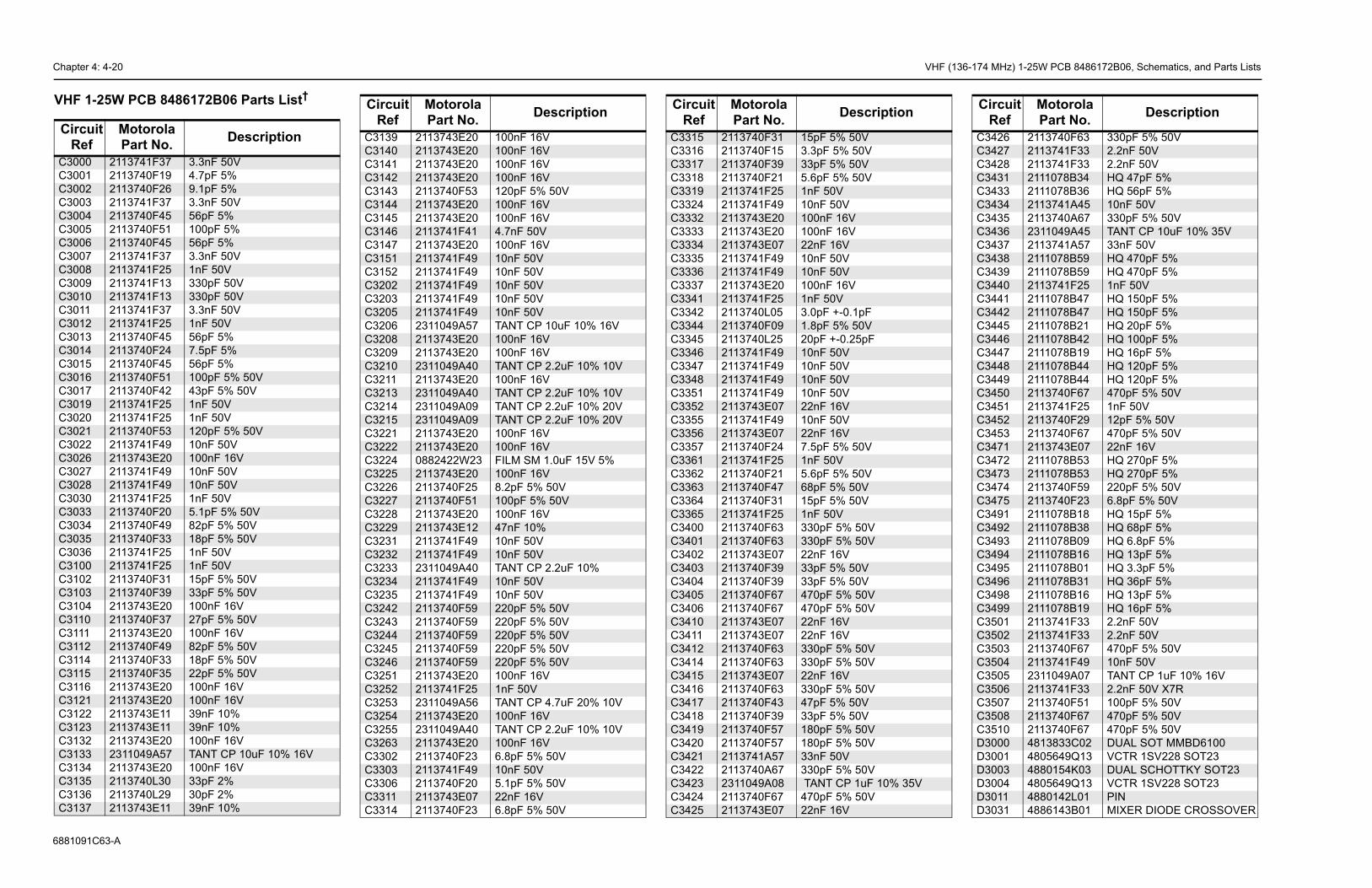
Chapter 4: 4-20 VHF (136-174 MHz) 1-25W PCB 8486172B06, Schematics, and Parts Lists
688109
VHF 1 †
CircRe
C300C300C300C300C300C300C300C300C300C300C301C3011C301C301C301C301C301C301C301C302C302C302C302C302C302C303C303C303C303C303C310C310C310C310C3110C3111C3112C3114C3115C3116C312C312C312C313C313C313C313C313C313
% 50V% 50V
% 50V% 50V
V0V16V16V6V0V0V16VV-0.1pF% 50V-0.25pF0V0V0V0V6V0V6V% 50V
V% 50V
% 50V% 50VV5% 50V5% 50V6V% 50V% 50V5% 50V5% 50V6V6V5% 50V5% 50V6V5% 50V% 50V% 50V5% 50V5% 50V0V5% 50VCP 1uF 10% 35V5% 50V6V
Description
C3426 2113740F63 330pF 5% 50VC3427 2113741F33 2.2nF 50VC3428 2113741F33 2.2nF 50VC3431 2111078B34 HQ 47pF 5%C3433 2111078B36 HQ 56pF 5%C3434 2113741A45 10nF 50VC3435 2113740A67 330pF 5% 50VC3436 2311049A45 TANT CP 10uF 10% 35VC3437 2113741A57 33nF 50VC3438 2111078B59 HQ 470pF 5%C3439 2111078B59 HQ 470pF 5%C3440 2113741F25 1nF 50VC3441 2111078B47 HQ 150pF 5%C3442 2111078B47 HQ 150pF 5%C3445 2111078B21 HQ 20pF 5%C3446 2111078B42 HQ 100pF 5%C3447 2111078B19 HQ 16pF 5%C3448 2111078B44 HQ 120pF 5%C3449 2111078B44 HQ 120pF 5%C3450 2113740F67 470pF 5% 50VC3451 2113741F25 1nF 50VC3452 2113740F29 12pF 5% 50VC3453 2113740F67 470pF 5% 50VC3471 2113743E07 22nF 16VC3472 2111078B53 HQ 270pF 5%C3473 2111078B53 HQ 270pF 5%C3474 2113740F59 220pF 5% 50VC3475 2113740F23 6.8pF 5% 50VC3491 2111078B18 HQ 15pF 5%C3492 2111078B38 HQ 68pF 5%C3493 2111078B09 HQ 6.8pF 5%C3494 2111078B16 HQ 13pF 5%C3495 2111078B01 HQ 3.3pF 5%C3496 2111078B31 HQ 36pF 5%C3498 2111078B16 HQ 13pF 5%C3499 2111078B19 HQ 16pF 5%C3501 2113741F33 2.2nF 50VC3502 2113741F33 2.2nF 50VC3503 2113740F67 470pF 5% 50VC3504 2113741F49 10nF 50VC3505 2311049A07 TANT CP 1uF 10% 16VC3506 2113741F33 2.2nF 50V X7RC3507 2113740F51 100pF 5% 50VC3508 2113740F67 470pF 5% 50VC3510 2113740F67 470pF 5% 50VD3000 4813833C02 DUAL SOT MMBD6100D3001 4805649Q13 VCTR 1SV228 SOT23D3003 4880154K03 DUAL SCHOTTKY SOT23D3004 4805649Q13 VCTR 1SV228 SOT23D3011 4880142L01 PIND3031 4886143B01 MIXER DIODE CROSSOVER
Circuit Ref
Motorola Part No. Description
1C63-A
-25W PCB 8486172B06 Parts List
uit f
Motorola Part No. Description
0 2113741F37 3.3nF 50V1 2113740F19 4.7pF 5%2 2113740F26 9.1pF 5%3 2113741F37 3.3nF 50V4 2113740F45 56pF 5%5 2113740F51 100pF 5%6 2113740F45 56pF 5%7 2113741F37 3.3nF 50V8 2113741F25 1nF 50V9 2113741F13 330pF 50V0 2113741F13 330pF 50V
2113741F37 3.3nF 50V2 2113741F25 1nF 50V3 2113740F45 56pF 5%4 2113740F24 7.5pF 5%5 2113740F45 56pF 5%6 2113740F51 100pF 5% 50V7 2113740F42 43pF 5% 50V9 2113741F25 1nF 50V0 2113741F25 1nF 50V1 2113740F53 120pF 5% 50V2 2113741F49 10nF 50V6 2113743E20 100nF 16V7 2113741F49 10nF 50V8 2113741F49 10nF 50V0 2113741F25 1nF 50V3 2113740F20 5.1pF 5% 50V4 2113740F49 82pF 5% 50V5 2113740F33 18pF 5% 50V6 2113741F25 1nF 50V0 2113741F25 1nF 50V2 2113740F31 15pF 5% 50V3 2113740F39 33pF 5% 50V4 2113743E20 100nF 16V
2113740F37 27pF 5% 50V2113743E20 100nF 16V2113740F49 82pF 5% 50V2113740F33 18pF 5% 50V2113740F35 22pF 5% 50V2113743E20 100nF 16V
1 2113743E20 100nF 16V2 2113743E11 39nF 10%3 2113743E11 39nF 10%2 2113743E20 100nF 16V3 2311049A57 TANT CP 10uF 10% 16V4 2113743E20 100nF 16V5 2113740L30 33pF 2%6 2113740L29 30pF 2%7 2113743E11 39nF 10%
C3139 2113743E20 100nF 16VC3140 2113743E20 100nF 16VC3141 2113743E20 100nF 16VC3142 2113743E20 100nF 16VC3143 2113740F53 120pF 5% 50VC3144 2113743E20 100nF 16VC3145 2113743E20 100nF 16VC3146 2113741F41 4.7nF 50VC3147 2113743E20 100nF 16VC3151 2113741F49 10nF 50VC3152 2113741F49 10nF 50VC3202 2113741F49 10nF 50VC3203 2113741F49 10nF 50VC3205 2113741F49 10nF 50VC3206 2311049A57 TANT CP 10uF 10% 16VC3208 2113743E20 100nF 16VC3209 2113743E20 100nF 16VC3210 2311049A40 TANT CP 2.2uF 10% 10VC3211 2113743E20 100nF 16VC3213 2311049A40 TANT CP 2.2uF 10% 10VC3214 2311049A09 TANT CP 2.2uF 10% 20VC3215 2311049A09 TANT CP 2.2uF 10% 20VC3221 2113743E20 100nF 16VC3222 2113743E20 100nF 16VC3224 0882422W23 FILM SM 1.0uF 15V 5%C3225 2113743E20 100nF 16VC3226 2113740F25 8.2pF 5% 50VC3227 2113740F51 100pF 5% 50VC3228 2113743E20 100nF 16VC3229 2113743E12 47nF 10%C3231 2113741F49 10nF 50VC3232 2113741F49 10nF 50VC3233 2311049A40 TANT CP 2.2uF 10%C3234 2113741F49 10nF 50VC3235 2113741F49 10nF 50VC3242 2113740F59 220pF 5% 50VC3243 2113740F59 220pF 5% 50VC3244 2113740F59 220pF 5% 50VC3245 2113740F59 220pF 5% 50VC3246 2113740F59 220pF 5% 50VC3251 2113743E20 100nF 16VC3252 2113741F25 1nF 50VC3253 2311049A56 TANT CP 4.7uF 20% 10VC3254 2113743E20 100nF 16VC3255 2311049A40 TANT CP 2.2uF 10% 10VC3263 2113743E20 100nF 16VC3302 2113740F23 6.8pF 5% 50VC3303 2113741F49 10nF 50VC3306 2113740F20 5.1pF 5% 50VC3311 2113743E07 22nF 16VC3314 2113740F23 6.8pF 5% 50V
Circuit Ref
Motorola Part No. Description
C3315 2113740F31 15pF 5C3316 2113740F15 3.3pF 5C3317 2113740F39 33pF 5C3318 2113740F21 5.6pF 5C3319 2113741F25 1nF 50C3324 2113741F49 10nF 5C3332 2113743E20 100nF C3333 2113743E20 100nF C3334 2113743E07 22nF 1C3335 2113741F49 10nF 5C3336 2113741F49 10nF 5C3337 2113743E20 100nF C3341 2113741F25 1nF 50C3342 2113740L05 3.0pF +C3344 2113740F09 1.8pF 5C3345 2113740L25 20pF +C3346 2113741F49 10nF 5C3347 2113741F49 10nF 5C3348 2113741F49 10nF 5C3351 2113741F49 10nF 5C3352 2113743E07 22nF 1C3355 2113741F49 10nF 5C3356 2113743E07 22nF 1C3357 2113740F24 7.5pF 5C3361 2113741F25 1nF 50C3362 2113740F21 5.6pF 5C3363 2113740F47 68pF 5C3364 2113740F31 15pF 5C3365 2113741F25 1nF 50C3400 2113740F63 330pF C3401 2113740F63 330pF C3402 2113743E07 22nF 1C3403 2113740F39 33pF 5C3404 2113740F39 33pF 5C3405 2113740F67 470pF C3406 2113740F67 470pF C3410 2113743E07 22nF 1C3411 2113743E07 22nF 1C3412 2113740F63 330pF C3414 2113740F63 330pF C3415 2113743E07 22nF 1C3416 2113740F63 330pF C3417 2113740F43 47pF 5C3418 2113740F39 33pF 5C3419 2113740F57 180pF C3420 2113740F57 180pF C3421 2113741A57 33nF 5C3422 2113740A67 330pF C3423 2311049A08 TANT C3424 2113740F67 470pF C3425 2113743E07 22nF 1
Circuit Ref
Motorola Part No.

V Chapter 4: 4-21
6881091C63-A
0 1/16W 5%0 1/16W 5%20 1/16W 5%7k 1/16W 5%60 1/16W 5%90 1/16W 5%500 1/16W 5%0k 1/16W 5%0k 1/16W 5%90 1/16W 5%1 1/16W 5% 1/16W 2k 1/16W 5%0 1/16W 5%00 1/16W 5%7k 1/16W 5%800 1/16W 5%20 OHMS 5%2k 1/16W 5% 0 1/16W 5%30 1/16W 5%90 1/16W 5%30 1/16W 5%7k 1/16W 5%800 1/16W 5%1 1/16W 5%5k 1/16W 5%200 1/16W 5%0k 1/16W 5%200 1/16W 5%90 1/16W 5%800 1/16W 5%400 1/16W 5%300 1/16W 5%80 OHMS 5%2k 1/16W 5%0k 1/16W 5%0k 1/16W 5%0k 1/16W 5%0k 1/16W 5%7 1/16W 5%7 1/16W 5%7 1/16W 5% 1/16W90 1/16W 5%HIP RES 680 OHMS 5%00 1/16W 5%7k 1/16W 5%7k 1/16W 5%00k 1/16W00 1/16W 5%
Description
R3242 0662057B47 0 1/16WR3251 0662057B04 180k 1/16W 5%R3252 0662057B10 330k 1/16W 5%R3261 0662057A89 47k 1/16W 5%R3263 0662057A65 4700 1/16W 5%R3301 0662057A22 75 1/16W 5%R3302 0662057A25 100 1/16W 5%R3303 0662057A57 2200 1/16W 5%R3304 0662057A49 1k 1/16W 5%R3308 0662057B47 0 1/16WR3311 0662057A25 100 1/16W 5%R3316 0662057B47 0 1/16WR3318 0662057A09 22 1/16W 5%R3321 0662057A73 10k 1/16W 5%R3323 0662057A49 1k 1/16W 5%R3331 0662057A17 47 1/16W 5%R3335 0662057A13 33 1/16W 5%R3336 0662057A77 15k 1/16W 5%R3341 0662057A33 220 1/16W 5%R3342 0662057A15 39 1/16W 5%R3343 0662057A25 100 1/16W 5%R3351 0662057A80 20k 1/16W 5%R3352 0662057A75 12k 1/16W 5%R3353 0662057A97 100k 1/16WR3354 0662057B02 150k 1/16WR3355 0662057A80 20k 1/16W 5%R3356 0662057A75 12k 1/16W 5%R3361 0662057A33 220 1/16W 5%R3362 0662057A17 47 1/16W 5%R3364 0662057A89 47k 1/16W 5%R3400 0662057A41 470 1/16W 5%R3401 0662057A36 300 1/16W 5%R3402 0662057A05 15 1/16W 5%R3403 0662057A36 300 1/16W 5%R3404 0662057A89 47k 1/16W 5%R3405 0662057A25 100 1/16W 5%R3406 0662057A97 100k 1/16WR3412 0662057A67 5600 1/16W 5%R3413 0662057A61 3300 1/16W 5%R3414 0683962T51 120 1W 5%R3415 0662057A25 100 1/16W 5%R3416 0662057A25 100 1/16W 5%R3418 0662057A81 22k 1/16W 5%R3421 0662057A87 39k 1/16W 5%R3422 0662057A57 2200 1/16W 5%R3423 0662057A87 39k 1/16W 5%R3424 0662057C13 2.7 1/10W 5%R3425 0662057C13 2.7 1/10W 5%R3426 0662057C13 2.7 1/10W 5%R3427 0662057C13 2.7 1/10W 5%R3428 0662057A58 2400 1/16W 5%
Circuit Ref
Motorola Part No. Description
HF (136-174 MHz) 1-25W PCB 8486172B06, Schematics, and Parts Lists
D3101 4880154K03 DIODE DUAL SCHOTTKYD3201 4802233J09 TRIPLE SOT143-RHD3221 4880236E05 CHIP SCHOTTKYD3341 4805649Q13 VCTR 1SV228 SOT23D3361 4805649Q13 VCTR 1SV228 SOT23D3362 4862824C01 VARACTOR CHIPD3401 4813833C02 DUAL SOT MMBD6100D3451 4880236E05 CHIP SCHOTTKYD3471 4802482J02 PIN MA/COMD3472 4802482J02 PIN MA/COMFL3101 9180112R16 44.85 MHZ XTAL FLTR 80dBFL3102 9180112R16 44.85 MHZ XTAL FLTR 80dBFL3111 9180469V03 CER FLTR 6EL 455 KHZ SMDFL3112 9180469V06 CER FLTR 6EL 455 KHZ SMDFL3113 9180468V04 CER FLTR 4EL 455 KHZ SMDFL3114 9180468V06 CER FLTR 4EL 455 KHZ SMDJ0401 0902636Y02 FLEX CONNECTORJ0451 0902636Y01 FLEX CONNECTORJ0501 0986105B01 ACCESSORY CONNECTORJ0551 0905505Y04 FLEX CONNECTORJ0552 0905505Y03 FLEX CONNECTORJ0601 0986165B01 DC POWER CONNECTORJ3401 0986166B02 RF CONN MINI UHFL3002 2462587T23 COIL CHIP 470nHL3031 2462587T24 COIL CHIP 560nHL3032 2462587T17 COIL CHIP 150nHL3101 2462587T25 COIL CHIP 620nHL3111 2462587T25 COIL CHIP 620nHL3112 2462587T25 COIL CHIP 620nHL3201 2462587Q42 IND CHIP 390nH 10%L3231 2462587Q20 IND CHIP 2.2uH 20%L3301 2462587N44 CHIP IND 18 NH 5%L3302 2462587N53 CHIP IND 100 nH 5%L3317 2462587V28 CHIP IND 33 NH 5%L3318 2462587V34 IND CHIP 100nH 5%L3331 2462587V32 CHIP IND 68NH 5%L3332 2462587V15 IND CHIP 100nH 10%L3333 2462587Q47 IND CHIP 1uH 10%L3341 2484562T13 MINI-SPRING AW IND
8NH 2%L3343 2462587N56 COIL CHIP 180nH 5%L3344 2462587N68 CHIP IND 1 uH 5%L3345 2462587N68 CHIP IND 1 uH 5%L3346 2484562T18 MINI-SPRING AW IND
35.5NH 2%L3351 2462587N68 CHIP IND 1 uH 5%L3361 2462587N50 CHIP IND 56 nH 5%L3362 2462587N51 CHIP IND 68 nH 5%L3363 2462587N50 CHIP IND 56 nH 5%L3364 2462587N68 CHIP IND 1 uH 5%L3401 2460591A01 SQUARE COIL 4.22nH 3T
Circuit Ref
Motorola Part No. Description
L3402 2484657R01 Ferrite BeadL3403 2462587T13 COIL CHIP 68nHL3411 2462587T13 COIL CHIP 68nHL3412 2462587X43 IND CHIP LO-PRO 15.0L3413 2460591B04 SQUARE COIL 11.03nH 4TL3414 2460591A11 SQUARE COIL 7.66nH 3TL3421 2484657R01 Ferrite BeadL3422 2460591C23 SQUARE COIL 16nH 3TL3436 2484657R01 Ferrite BeadL3437 2460592A01 COIL AW 17nH 2TL3443 2460591X02 COIL SQUARE 25nHL3471 2462587X69 IND CHIP 1.2uH 5%L3472 2460592B01 COIL AW 51nH 4TL3491 2460592B01 COIL AW 51nH 4TL3492 2460592B01 COIL AW 51nH 4TL3493 2460592B01 COIL AW 51nH 4TM3421 2686201B01 HEAT SPREADERQ3001 4813827A07 TSTR NPN SML SIG MMBR9Q3002 4813824A17 TSTR PNP 40V .2A B=100-Q3021 4805921T02 TSTR DUAL ROHM FMC2Q3101 4813827A07 TSTR NPN SML SIG MMBR9Q3102 4813827A07 TSTR NPN SML SIG MMBR9Q3141 4813824A10 TSTR NPN 40V .2A B=50-150Q3151 4880048M01 TSTR NPN DIG 47k/47kQ3152 4880048M01 TSTR NPN DIG 47k/47kQ3221 4880048M01 TSTR NPN DIG 47k/47kQ3301 4813827A07 TSTR NPN SML SIG MMBR9Q3303 4802245J50 TSTR DUAL NPN/PNP
UMC5NQ3304 4805218N63 RF TRANS SOT 323
BFQ67WQ3411 4805921T02 DUAL ROHM FMC2 RHQ3421 4802245J55 MRF1507Q3422 4880048M01 NPN DIG 47k/47kQ3441 4886136B01 LDMOS PWR TSTR
MRF1565 MRF1550Q3442 4880048M01 NPN DIG 47k/47kQ3471 4880048M01 NPN DIG 47k/47kQ3472 4805128M27 PNP SOT89 BSR33 LHR3000 0662057A53 1500 1/16W 5%R3001 0662057A97 100k 1/16WR3002 0662057A43 560 1/16W 5%R3003 0662057A49 1k 1/16W 5%R3004 0662057A53 1500 1/16W 5%R3006 0662057A73 10k 1/16W 5%R3009 0662057A97 100k 1/16WR3010 0662057A45 680 OHMS 5%R3011 0662057A65 4700 1/16W 5%R3012 0662057A49 1k 1/16W 5%R3013 0662057A61 3300 1/16W 5%R3014 0662057A18 51 1/16W 5%
Circuit Ref
Motorola Part No. Description
R3015 0662057A01 1R3016 0662057A01 1R3018 0662057A33 2R3019 0662057A89 4R3021 0662057A43 5R3024 0662057A39 3R3025 0662057A53 1R3026 0662057A73 1R3027 0662057A73 1R3028 0662057A39 3R3031 0662057A18 5R3033 0662057B47 0R3101 0662057A75 1R3102 0662057A01 1R3105 0662057A25 1R3106 0662057A83 2R3107 0662057A69 6R3108 0662057A44 6R3111 0662057A75 1R3112 0662057A01 1R3113 0662057A37 3R3115 0662057A39 3R3116 0662057A37 3R3117 0662057A83 2R3118 0662057A69 6R3130 0662057A18 5R3132 0662057A77 1R3133 0662057A71 8R3134 0662057A73 1R3135 0662057A51 1R3141 0662057A39 3R3142 0662057A55 1R3144 0662057A58 2R3145 0662057A61 3R3146 0662057A45 6R3147 0662057A75 1R3151 0662057A73 1R3152 0662057A73 1R3153 0662057A73 1R3154 0662057A73 1R3201 0662057A17 4R3203 0662057A17 4R3204 0662057A17 4R3211 0662057B47 0R3221 0662057A39 3R3222 0662057A45 CR3223 0662057A25 1R3224 0662057A89 4R3225 0662057A89 4R3227 0662057A97 1R3241 0662057A25 1
Circuit Ref
Motorola Part No.
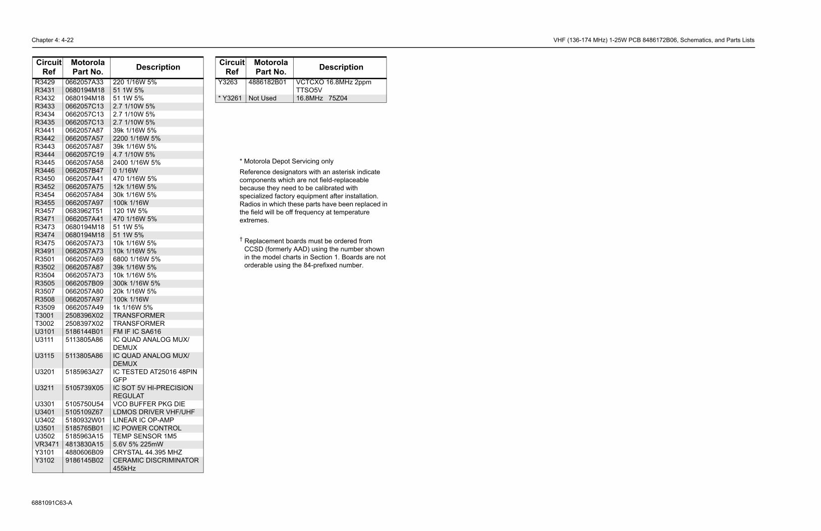
Chapter 4: 4-22 VHF (136-174 MHz) 1-25W PCB 8486172B06, Schematics, and Parts Lists
688109
R342R343R343R343R343R343R344R344R344R344R344R344R345R345R345R345R345R347R347R347R347R349R350R350R350R350R350R350R350T3001T3002U310U3111
U3115
U320
U3211
U330U340U340U350U350VR34Y3101Y3102
CircRe
1C63-A
* Motorola Depot Servicing onlyReference designators with an asterisk indicate components which are not field-replaceable because they need to be calibrated with specialized factory equipment after installation. Radios in which these parts have been replaced in the field will be off frequency at temperature extremes.
† Replacement boards must be ordered from CCSD (formerly AAD) using the number shown in the model charts in Section 1. Boards are not orderable using the 84-prefixed number.
9 0662057A33 220 1/16W 5%1 0680194M18 51 1W 5%2 0680194M18 51 1W 5%3 0662057C13 2.7 1/10W 5%4 0662057C13 2.7 1/10W 5%5 0662057C13 2.7 1/10W 5%1 0662057A87 39k 1/16W 5%2 0662057A57 2200 1/16W 5%3 0662057A87 39k 1/16W 5%4 0662057C19 4.7 1/10W 5%5 0662057A58 2400 1/16W 5%6 0662057B47 0 1/16W0 0662057A41 470 1/16W 5%2 0662057A75 12k 1/16W 5%4 0662057A84 30k 1/16W 5%5 0662057A97 100k 1/16W7 0683962T51 120 1W 5%1 0662057A41 470 1/16W 5%3 0680194M18 51 1W 5%4 0680194M18 51 1W 5%5 0662057A73 10k 1/16W 5%1 0662057A73 10k 1/16W 5%1 0662057A69 6800 1/16W 5%2 0662057A87 39k 1/16W 5%4 0662057A73 10k 1/16W 5%5 0662057B09 300k 1/16W 5%7 0662057A80 20k 1/16W 5%8 0662057A97 100k 1/16W9 0662057A49 1k 1/16W 5%
2508396X02 TRANSFORMER2508397X02 TRANSFORMER
1 5186144B01 FM IF IC SA6165113805A86 IC QUAD ANALOG MUX/
DEMUX5113805A86 IC QUAD ANALOG MUX/
DEMUX1 5185963A27 IC TESTED AT25016 48PIN
GFP5105739X05 IC SOT 5V HI-PRECISION
REGULAT1 5105750U54 VCO BUFFER PKG DIE1 5105109Z67 LDMOS DRIVER VHF/UHF2 5180932W01 LINEAR IC OP-AMP1 5185765B01 IC POWER CONTROL2 5185963A15 TEMP SENSOR 1M571 4813830A15 5.6V 5% 225mW
4880606B09 CRYSTAL 44.395 MHZ9186145B02 CERAMIC DISCRIMINATOR
455kHz
uit f
Motorola Part No. Description
Y3263 4886182B01 VCTCXO 16.8MHz 2ppm TTSO5V
* Y3261 Not Used 16.8MHz 75Z04
Circuit Ref
Motorola Part No. Description
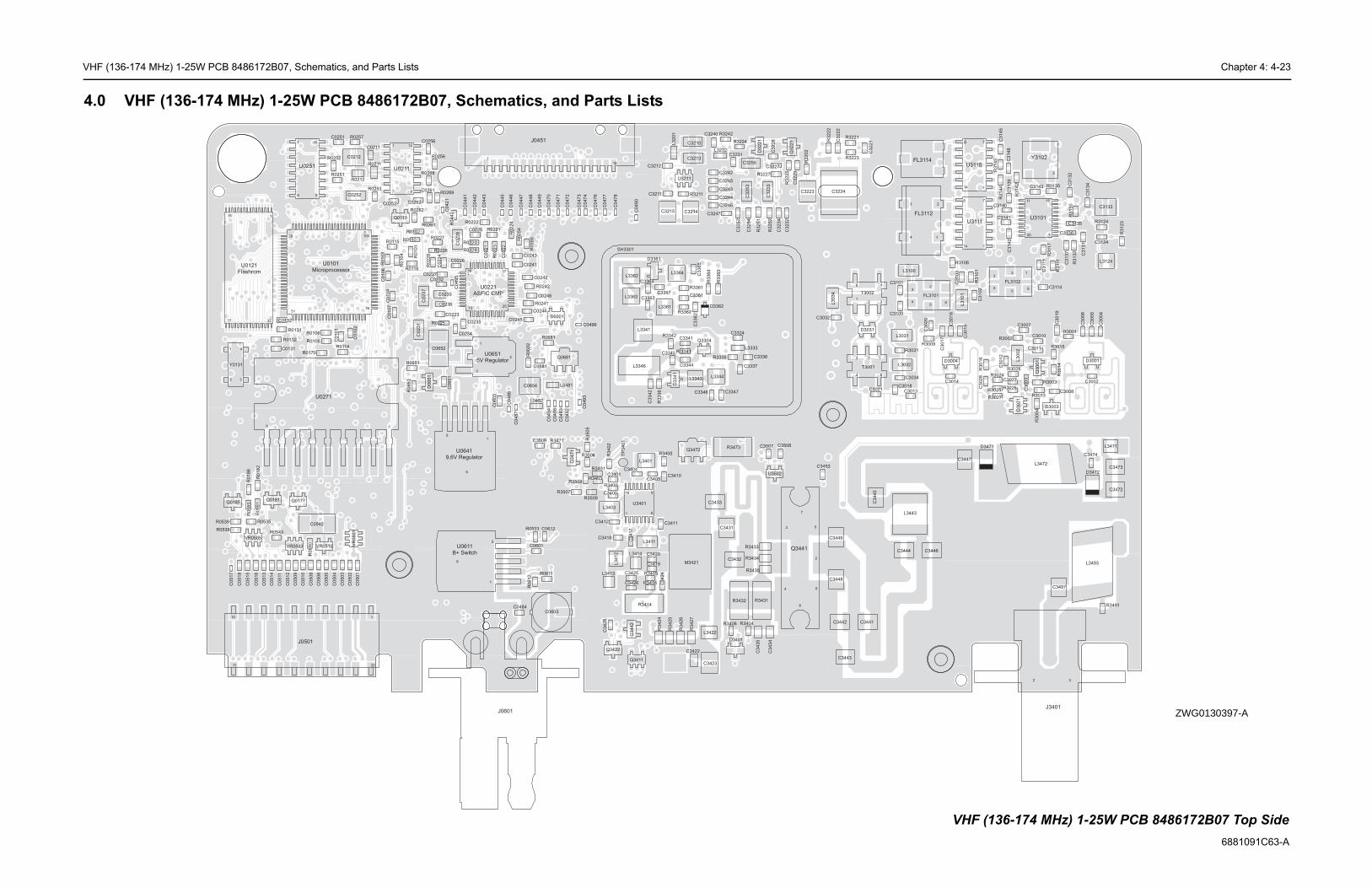
VHF (136-174 MHz) 1-25W PCB 8486172B07, Schematics, and Parts Lists Chapter 4: 4-23
6881091C63-A
4
ZWG0130397-A
C3002
C3
00
4
C3
00
5
C3
00
6
C3007
C3008C3
00
9
C3010
C3011
C3
01
2
C3013
C3014
C3
01
5C3
01
6
C3
01
7
C3018
C3
01
9
C3
02
0
C3021
C3027
C3
02
8C3034
C3100
C3101
C3
10
2
C3
10
3
C3114
C3
11
5
C3124
C3
13
1
C3
13
2
C3133
C3
13
4
C3135
C3136
C3
13
7
C3
13
9
C3140
C3141
C3
14
2
C3143
C3
14
5
C3
14
8
C3
22
1C3
22
2
3224
C34413442
C3443
C3444
C3
44
5
C3446
C3447
448
449
C3472
C3473
C3474
C3497
D3001
D3003
D3004
D3031
D3471
D3472
23
45
6
FL3101
23
45
6
FL3102
4
3 2
FL3112
FL3114
2 3
J3401
L3
00
2
L3031
L3032
L3
03
4
L3100
L3101
L3124
L3443
L3471
L3472
L3493
Q3001
Q3
02
1
R3001
R3002
R3003
R3
00
4
R3009
R3013
R3
01
4
R3015
R3
01
6
R3024
R3025R3026
R3027
R3028
R3031
R3
10
1
R3106
R3
111
R3
11
7
R3
12
3R3124
R3
13
0R
31
32
R3135
R3
14
2
R3
14
4R
31
45
R3221
R3223
R3491
3
4 6
12
T3001
3
46
12
T3002
11
120
10
U3101
8 7
114
U3111
8 7
114
U3115
2
Y3102
1
1
ZW
G0
13
03
97
-A
VHF (136-174 MHz) 1-25W PCB 8486172B07 Top Side
.0 VHF (136-174 MHz) 1-25W PCB 8486172B07, Schematics, and Parts Lists
C0101
C0
10
2
C0
10
4C
01
06
C0
10
7
C0131
C0132
C0211
C0212
C0
22
1
C0222
C0223
C0
22
4
C0225
C0226
C0227
C0
22
8
C0
23
1
C0232
C0233
C0234
C0235
C0236
C0
23
7
C0241
C0242
C0243
C0244
C0245
C0246
C0251
C0252
C0253
C0256
C0261
C0262
C0
42
1
C0
44
1
C0
44
2
C0
44
3
C0
44
5
C0
44
6
C0
44
7
C0
44
8
C0
44
9
C0
47
0
C0
47
1
C0
47
2
C0
47
3
C0
47
4
C0
47
6
C0
47
7
C0
47
8
C0
48
2
C0
48
3
C0484
C0
48
6
C0
48
7
C0
48
8
C0
49
0
C0
49
3
C0
49
4
C0
49
5
C0496
C0
50
1
C0
50
2
C0
50
3
C0
50
4
C0
50
5
C0
50
6
C0
50
8
C0
50
9
C0
51
0
C0
511
C0
51
2
C0
51
3
C0
51
4
C0
51
5
C0
51
6
C0
51
7
C0
51
8
C0542
C0601
C0603
C0612
C0
65
1
C0652
C0654
C0
65
5
C0681
C3032
C3210
C3211
C3212
C3213
C3215
C3223 C
C3
22
6
C3227
C3
22
9
C3231
C3
23
2
C3
23
3
C3
23
4
C3240
C3242
C3243
C3244
C3245
C3246
C3247
C3
25
2
C3
25
3C
32
54
C3255
C3324
C3336
C3337
C3341
C3
34
2
C3344
C3345
C3346 C3347
C3357C3361
C3
36
2
C3363
C3364
C3
36
5
C3400
C3401C3403
C3404
C3410
C3411C3412
C3
41
7
C3418
C3419
C3420
C3422
C3423C
34
24C3425
C3426
C3
42
8
C3431
C3432
C3433
C3
43
4
C3
43
5
C
C3
C3
C3453
C3507 C3508C3509
D0201
D0
65
1
D3
22
1
D3
34
1
D3361
D3362
D3401
18
1
2011
10
J0601
L0481
L0482
L3
20
1
L3232
L3333
L3341
L3343 L3344
L3346
L3361
L3362
L3363
L3364
L3401
L3403
L3411
L3
41
2
L3413
L3414
L3422
M3421
Q0110
Q0177Q0181Q0185
Q0681
Q3
22
1
Q3304
Q3411
Q3422
2
3
4
5
6
7
8
Q3441
Q3
44
2
Q3
47
1 Q3472
R0101
R0102
R0
10
4
R0105
R0106
R0
10
8
R0110
R0114
R0115
R0116
R0131
R0132
R0170
R0
18
1R
01
82
R0
18
5R
01
86
R0211
R0212
R0220
R0221
R0222
R0
22
3
R0
22
4
R0225
R0226
R0227
R0
22
8
R0229
R0241
R0242
R0251
R0252
R0253
R0
25
4
R0
25
5
R0256
R0257
R0261
R0262
R0268
R0269
R0
44
2
R0
51
0
R0533
R0535
R0538
R0539
R0543
R0611
R0
61
2
R0651
R0
65
2
R0681
R0
68
2
R3
20
2
R3211
R3222
R3224
R3
22
5
R3227
R3242
R3
25
1
R3
25
2
R3335
R3
33
6
R 3341
R3342
R3361
R3362
R3
36
3
R3
36
4
R3400
R3401
R3
40
2
R3403
R3404
R3405
R3406
R3414
R3415
R3416
R3
42
4
R3
42
5
R3
42
6
R3
42
7
R3431R3432
R3433
R3434
R3435
R3471
R3473
R3
50
5
R3506
R3507
R3508
R3509
SH3301
TP
3401
1
7651
26
3217
16 1
87
1 14
U0211
137
2513
161
8 9
9
1
6
5
1
6
5
3
2
1
U3211
1
16
8
9
U3401
U3502
VR
0501
VR0503
VR0505
VR0510
2 3
4
Y0131
1
1
100
1
C3214
48
J0451
J0501
U0251
U0271
U0101Microprocessor
U0121Flashrom
U0221ASFIC CMP
U0611B+ Switch
U06419,6V Regulator
U06515V Regulator
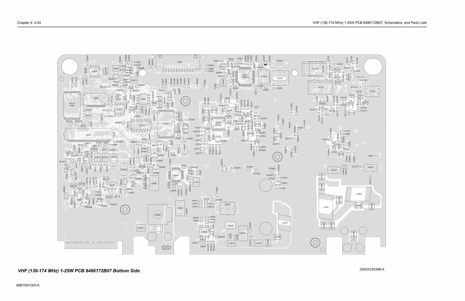
Chapter 4: 4-24 VHF (136-174 MHz) 1-25W PCB 8486172B07, Schematics, and Parts Lists
6881091
C3000
C3001
C3
02
2
C3
02
5
C3
02
6
C3
02
9
C3030
C3033
C3
03
5
C3
03
6
C3
10
4C
311
0 C3111
C3112
C3
11
3
C3116
C3121
C3122 C3123
C3144
C3
14
6
C3
14
7
C3
15
1C
31
52
C3
45
0
3451
52
C3471
C3
47
5C3
49
1C
34
92
C3
49
3
C3
49
4
C3495
C3
49
6
C3
49
8
C3
49
9
D3000
D3
011
D3101
3451
43
2
FL3111
FL
311
3
43
2
FL3115
L3
02
5
L3111
L3112
3437
L3491
L3492
Q3002
Q3101 Q3102
Q3
14
1
Q3151
Q3152
R3000
R3
00
6
R3010
R3
011
R3012
R3018
R3
02
1
R3
02
3
R3030
R3032
R3033
R3034
R3
03
5
R3
03
6
R3
10
2
R3
10
4
R3
10
5
R3107R3108
R3
11
2
R3113
R3114
R3115
R3116R3118
R3133
R3134
R3141
R3
14
6
R3147
R3
15
1
R3152
R3153
R3
15
4
R3
45
0R3457
R3474
TP
3001
4 3
2
Y3101
2
3
1
1
1
VHF ( ZWG0130398-A
C63-A
C0103
C0
10
5
C0111
C0
11
2
C0
12
1
C0
12
2
C0
12
3
C0
14
1
C0
15
1
C0201
C0202
C0203
C0204
C0
20
5
C0254
C0
25
5
C0265
C0
26
6
C0267
C0
27
1
C0
27
2
C0
27
3
C0
27
4
C0275
C0
27
6
C0
27
7
C0301
C0302
C0303
C0
30
4
C0
30
5
C0
32
4
C0
32
5
C0331
C0
34
1
C0
34
2
C0343
C0
34
4
C0351
C0352
C0
35
3
C0354
C0
42
2
C0
42
3
C0
42
6
C0
42
7
C0
42
8
C0
42
9
C0
43
0
C0
43
1
C0
48
5
C0491
C0492
C0497
C0
49
9
C0541
C0
55
4 C0558C0559
C0560
C0575C0576
C0591
C0592C0593
C0611
C0621
C0622
C0641
C0
64
4
C0645
C0661
C0662
C0
66
3
C0671
C3003
C3
02
3C
30
24
C3031
C3
20
2
C3203
C3
20
5 C3
20
6
C3
20
7
C3
20
8
C3209
C3
22
5
C3
22
8
C3235
C3241
C3251
C3
26
1
C3
26
2
C3
26
3
C3301
C3302
C3303
C3304
C3
30
5
C3
30
6
C3311
C3312
C3313
C3314
C3315
C3316
C3317
C3
31
8C
33
19
C3331
C3332
C3333
C3
33
4
C3
33
5
C3
34
8
C3
35
1C
33
52
C3
35
5
C3
35
6
C3
40
2
C3
40
5
C3
40
6
C3413
C3414 C3415
C3416C
34
21
C3
42
7
C3436
C3
43
7
C3438
C3
43
9
C3440
C
C34
C3501
C3
50
2C3503
C3504
C3
50
5C
35
06
C3
51
0
D0101
D0151
D0179
D0301
D0
62
1
D0
66
0D
06
61
D3201
D3
26
1
D
E0271E0272
E0631
12
J0401
1 40
J0551
1 18
J0552
L3
23
1
L3301
L3302
L3311
L3317
L3318
L3331
L3332
L3345
L3351
L3402
L3421
L3436
L
Q0
15
1
Q0171
Q0173Q0183
Q0
27
1
Q0641
Q0661
Q0662 Q0663
Q3301
Q3302
43
Q3303
12 3
Q3421
R0107
R0111R0112
R0
11
3
R0
11
7
R0121
R0
15
1
R0152
R0
17
1
R0
17
2
R0
17
3
R0174
R0
17
5
R0
17
6
R0
17
7
R0
17
8
R0
17
9
R0
18
3R
01
84
R0201
R0202
R0203
R0204
R0205
R0206
R0207
R0
20
8
R0
26
5
R0266
R0267
R0
27
3
R0274
R0
27
5
R0
27
6
R0323
R0
32
4
R0331
R0
33
2
R0333
R0
33
5
R0
34
1
R0
34
2
R0343
R0344
R0345
R0
34
6
R0
34
7
R0
40
1
R0
40
7
R0408
R0
40
9
R0410
R0
41
2
R0
44
1
R0
46
7
R0
46
8
R0
48
1
R0482
R0511
R0
51
2 R0525R0
52
9
R0530
R0531
R0
53
7
R0
54
1
R0542
R0591
R0592
R0
59
3
R0621
R0641
R0642 R0
64
3
R0661 R0
66
2
R0
67
1
R0
67
2
R3
01
9
R3201
R3203
R3204
R3206
R3226
R3
22
8
R3
24
1
R3261
R3
26
2
R3263
R3301
R3302
R3303
R3
30
4
R3305
R3
30
6
R3307
R3
30
8
R3
311 R
33
12
R3313
R3
31
4
R3
31
5
R3316
R3
31
7
R3318
R3
31
9
R3321
R3323
R3331
R3343
R3
35
1R
33
52
R3
35
3
R3
35
4
R3
35
5
R3
35
6
R3411
R3412
R3
41
3
R3417
R3418
R3
42
1
R3
42
2
R3
42
3R
34
28
R3429
R3440
R3441
R3442R3443
R3444
R3445
R3
44
6
R3452
R3
45
4
R3455
R3475
R3501
R3502R3504
S3440
TP0101
TP0102
TP0103
TP
0104
TP0151
TP0221
TP0222
TP0492 TP
04
97
TP0530
TP0661
TP3201TP
32
02
TP
34
02
TP3403TP3404
TP3405
TP
34
06
1 4
58
U0111
22
218
7 1
16
1 8
9
U0141
2815
14 1
U0301
U0331
1
45
8
U0341
U0342
4
5 8
U0351
14
5 8
U0652
U0
65
3
137
2513
11
1
20
10
1 458
U3402
1
17
9
25
U3501
VR
01
51
VR0504VR0509
VR
05
37
VR0541
VR0601
VR
06
21 VR0671
VR
34
71
6
4 3
1
Y3261
4
Y3263
48
1
U0122RAM
U3201FRACN
U3301VCOIC
136-174 MHz) 1-25W PCB 8486172B07 Bottom Side
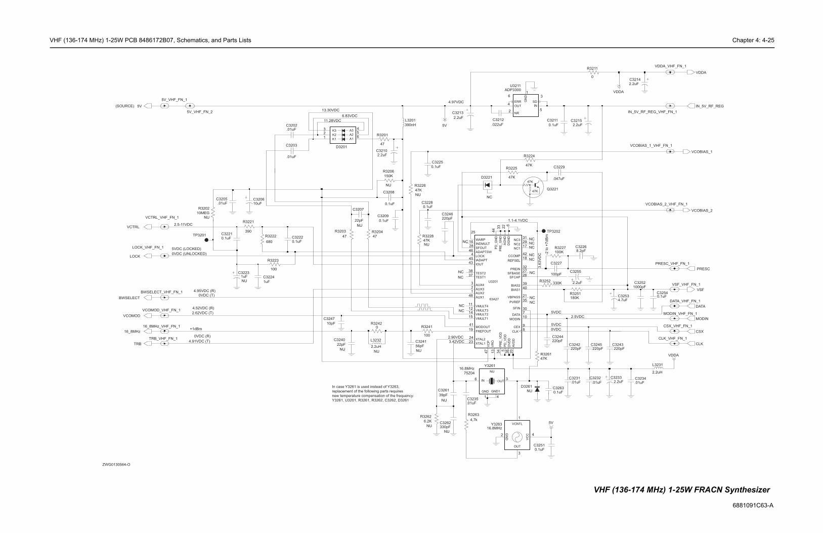
VHF (136-174 MHz) 1-25W PCB 8486172B07, Schematics, and Parts Lists Chapter 4: 4-25
6881091C63-A
47K
47K
0VDC
5VDC
5VDC
-2 to +
7dB
m
3.6
3V
DC
2.5VDC
1.1-4.1VDC
C3231.01uF
C3229
0.1uF
.047uF
CLK
C3251
47K
VCOBIAS_2
R3225
C32268.2pF
MODIN_VHF_FN_1
R3252
VCOBIAS_1_VHF_FN_1
330K
PRESC_VHF_FN_1
VSF_VHF_FN_1
DATA
CSX_VHF_FN_1
100pF
C3227
CSX
IN_5V_RF_REG_VHF_FN_1
3T
100KR3227
0.1uFC3254
.01uF
C3232
PRESC
C32142.2uF
C32630.1uF
27SFBASE
26SFCAP
30SFIN
21VBPASS
31NC3
PD
_V
DD
5
PREIN32
PR
E_
GN
DP
RE
_V
DD
35PVREF
18REFSEL
10MODIN
17NC1
29NC2
39BIAS2
42CCOMP
9CEX8
CLK
7DATA
DG
ND
63
6D
VD
D
22
AG
ND
20
AV
DD
40BIAS1
VCOBIAS_1
VSF
0
R3211
L3231
0.1uF
C3211
TP3202
2.2uH
C3243220pF
VDDA
VDDA_VHF_FN_1
VCOBIAS_2_VHF_FN_1
Q3221
R3251180K
220pFC3245
C3215
R3224
47K
2.2uF
1
GN
D
5IN
2NR
4OUT
3
SD
VC
C 4
VCNTL
1
ADP3300U3211
6
ERR
GN
D
2
OUT
3
MODIN
C3255
DATA_VHF_FN_1
220pFC3242
2.2uF
R326147K
2.2uFC3233
CLK_VHF_FN_1
C32521000pF
.01uFC3234
C32534.7uF
NU
IN_5V_RF_REG
D3261
C3244220pF
5V
NC
NC
NC
NC
NC
VDDA
VDDA
NCNCNC
F
2
VHF (136-174 MHz) 1-25W FRACN Synthesizer
(SOURCE)13.30VDC
6.83VDC
4.52VDC (R)
+1dBm
0VDC (R)
4.95VDC (R)
2.90VDC
3.42VDC
0VDC (T)
2.62VDC (T)
4.91VDC (T)
11.28VDC
4.97VDC
2.5-11VDC
5VDC (LOCKED)
0VDC (UNLOCKED)
R3203
A1
5A2
4A3
K11
K22
K33
47
D3201
6
47KNU
TRBL3232
2.2uH
NU
R3228
C3225
L3201
390nH
0.1uF
C3202.01uF
100
R3223
D3221
C3207
22pF
NU
TP3201
16_8MHz_VHF_FN_1R3242
0
100
R3241
VCOMOD_VHF_FN_1
22pF
NU
C3240
NU
1
GND
4
GND1
OU6 IN
16.8MHz
75Z04
Y3261
C3208
0.1uF
NU
47K
R3226
C32210.1uF
1uF
C3224
VMULT11514
VMULT2
12VMULT3
11VMULT4
VR
O1
3
25
WARP
23XTAL1
XTAL224
28SFOUT
37TEST1
38TEST2
47
VC
P
44
PD
_G
ND
33
34
45 IADAPT
16INDMULT
43 IOUT
LOCK4
41MODOUT
19FREFOUT
46 ADAPTSW
48AUX1
1AUX2
2AUX3
3AUX4
63A27
U3201
47
R3201
C32220.1uF
16_8MHz
0.1uF
C3209C3246220pF
NU
C320610uF
5V_VHF_FN_2
150K
R3206
.01uF
C32280.1uF
C3235
2.2uFC3210
VCTRL_VHF_FN_1
R3204
LOCK_VHF_FN_1
47
1uFC3223
NU
R3262
NU
BWSELECT
6.2K
C3213
2.2uF
Y326316.8MHz
VCTRL
5V_VHF_FN_1
.01uF
R3222
680
TRB_VHF_FN_1
C3205
C3262330pF
NU
NU
VCOMOD
C3241
56pF
R3221
390
5V
C3261
NU
LOCK
39pF
BWSELECT_VHF_FN_1
C3203
4,7k
.01uF
NC
5V
R3263
NC
NC
NC
NC
NC
.022u
C321
R3202
10MEG
NU
10pF
C3247
In case Y3261 is used instead of Y3263,
replacement of the following parts requires
new temperature compensation of the frequency:
Y3261, U3201, R3261, R3262, C3262, D3261
ZWG0130564-O
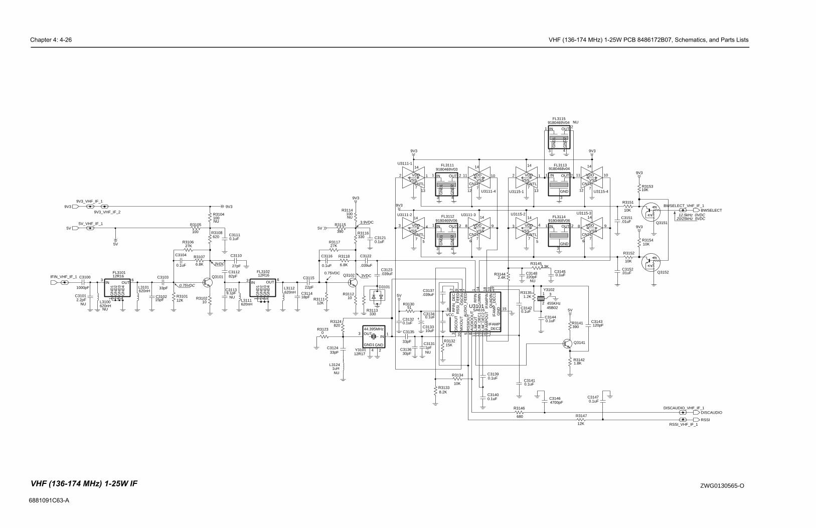
Chapter 4: 4-26 VHF (136-174 MHz) 1-25W PCB 8486172B07, Schematics, and Parts Lists
6881091
12.5kHz 0VDC20/25kHz 5VDC
9180469V04
9180468v04
9180468V06
R31351.2K
Q3151
680
R3146
U3115-1
CNTL
13
12 VDD
14
VSS
7
DISCAUDIO_VHF_IF_1
0.1uFC3144
120pFC3143
9
C31410.1uF
Q3141
3
GND
1 IN 2OUT
FL3113
0.1uFC3142
I
DISCAUDIO
R3151
0
10K
3
14
VDD
7
VSS
U3115-2
5
CNTL
4
Q3152C3152.01uF
.01uFC3151
4700pFC3146
390R3141
1.8KR3142
R315410K
15
P2
GN
D
R3147
12K
455KHz
3
2
1
BWSELECT_VHF_IF_1BWSELECT
45B02
Y3102
10K
R3152
U3115-3
6
CNTL
8 9
14
VDD
7
VSS
RSSI_VHF_IF_1
2.4K3144
3.3KR3145
C3145
C31470.1uF
0.1uF220pFC3148
NU
10VDD
14
VSS
7U3115-4
CNTL
12
11
FL3115
GN
D1
3 4
GN
D2
IN1 OUT 2NU
3GND
1 IN 2OUT
RSSI
FL3114
R315310K
9V3
9V3
9V3
5V
VHF ( ZWG0130565-O
C63-A
9180469V03
3.9VDC
0.75VDC
0.75VDC3VDC
9180469V06
3VDC6.8K
R3107
9V3
390
1G
ND
1G
ND
22
GN
D3
4 5G
ND
4
3IN
6OUT
R3115
FL310112R16
R311727K
Q3102
620nHL3111
620R3108
R3118
6.8K
R311112K
C3101
5V_VHF_IF_1
GN
D2
4
1 IN 2OUT
NU2.2pF
FL3111
3
GN
D1
15KR3132
C3130.1uF
13
12 VDD
14
VSS
7
U3111-1
CNTL
R3116330
10
9V3_VHF_IF_2
R3102
C3110
27pF
9.1pF
FIN_VHF_IF_1
100R3104
NU
C3113
1 2G
ND
24
GN
D3
GN
D4
5
IN3 OUT6
NU
12R16FL3102
GN
D11000pF
C3100
C3140.1uF
11 10VDD
14
VSS
7U3111-4
CNTL
12
R31338.2K
27KR3106
C311282pF
10R3112
C3122
.039uF
Q3101
6
VCC330R3113
20M
IXO
UT
4O
SC
IN
3O
SC
OU
T
10Q
UA
DIN
1R
FIN
2R
FIN
_DE
C
5R
SS
IOU
T
9R
SS
I_F
EE
D
18IF
AM
PIN
16IF
AM
PO
UT
19IF
AM
P_D
EC
1
17
IFAM_DEC
14LI
MIN
11LI
MO
UT
13LI
M_D
EC
112
LIM
_DE
C2
SA616U3101
8A
UD
IOO
UT
7A
UD
IO_F
EE
D
51
44.395MHz
12R17Y3101 2
GND4
GND1
3 OUT 1IN
R3130
C313630pF
C3135
33pF
12KR3101
C313310uF
C3115
100
R3105
22pF
620nHL3100
0.1uF
NU
C3137.039uF
C3134
C3103
33pF
C31320.1uF
0.1uFC3111
18pFC3114
L3112620nH
9V3_VHF_IF_1
5V
D3101
OUT
.039uFC3123
FL3112
3
GN
D1
GN
D2
4
1 IN 2
R3114100
R3134
10K
NU
R
U3111-2
5
CNTL
43
14
VDD
7
VSS
620nHL3101
NU1pF
C3131
C31210.1uF
15pFC3102
U3111-3
6
CNTL
8 9
14
VDD
7
VSS
C3116
0.1uF 0.1uF
C3104
5V
5V
9V3
9V39V3
5V
9V3
0R3123
1uHNU
L3124
33pFC3124
820R3124
136-174 MHz) 1-25W IF
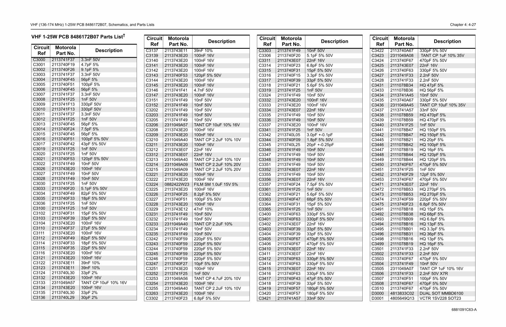
V Chapter 4: 4-27
6881091C63-A
V
0nF 50V.1pF 5% 50V2nF 16V.8pF 5% 50V5pF 5% 50V.3pF 5% 50V3pF 5% 50V.6pF 5% 50VnF 50V0nF 50V00nF 16V00nF 16V2nF 16V0nF 50V0nF 50V00nF 16VnF 50V.0pF +-0.1pF.8pF 5% 50V0pF +-0.25pF0nF 50V0nF 50V0nF 50V0nF 50V2nF 16V0nF 50V2nF 16V.5pF 5% 50VnF 50V.6pF 5% 50V8pF 5% 50V5pF 5% 50VnF 50V30pF 5% 50V30pF 5% 50V2nF 16V3pF 5% 50V3pF 5% 50V70pF 5% 50V70pF 5% 50V2nF 16V2nF 16V30pF 5% 50V30pF 5% 50V2nF 16V30pF 5% 50V7pF 5% 50V3pF 5% 50V80pF 5% 50V80pF 5% 50V3nF 50V
Description
C3422 2113740A67 330pF 5% 50VC3423 2311049A08 TANT CP 1uF 10% 35VC3424 2113740F67 470pF 5% 50VC3425 2113743E07 22nF 16VC3426 2113740F63 330pF 5% 50VC3427 2113741F33 2.2nF 50VC3428 2113741F33 2.2nF 50VC3431 2111078B34 HQ 47pF 5%C3433 2111078B36 HQ 56pF 5%C3434 2113741A45 10nF 50VC3435 2113740A67 330pF 5% 50VC3436 2311049A45 TANT CP 10uF 10% 35VC3437 2113741A57 33nF 50VC3438 2111078B59 HQ 470pF 5%C3439 2111078B59 HQ 470pF 5%C3440 2113741F25 1nF 50VC3441 2111078B47 HQ 150pF 5%C3442 2111078B47 HQ 150pF 5%C3445 2111078B21 HQ 20pF 5%C3446 2111078B42 HQ 100pF 5%C3447 2111078B19 HQ 16pF 5%C3448 2111078B44 HQ 120pF 5%C3449 2111078B44 HQ 120pF 5%C3450 2113740F67 470pF 5% 50VC3451 2113741F25 1nF 50VC3452 2113740F29 12pF 5% 50VC3453 2113740F67 470pF 5% 50VC3471 2113743E07 22nF 16VC3472 2111078B53 HQ 270pF 5%C3473 2111078B53 HQ 270pF 5%C3474 2113740F59 220pF 5% 50VC3475 2113740F23 6.8pF 5% 50VC3491 2111078B18 HQ 15pF 5%C3492 2111078B38 HQ 68pF 5%C3493 2111078B09 HQ 6.8pF 5%C3494 2111078B16 HQ 13pF 5%C3495 2111078B01 HQ 3.3pF 5%C3496 2111078B31 HQ 36pF 5%C3498 2111078B16 HQ 13pF 5%C3499 2111078B19 HQ 16pF 5%C3501 2113741F33 2.2nF 50VC3502 2113741F33 2.2nF 50VC3503 2113740F67 470pF 5% 50VC3504 2113741F49 10nF 50VC3505 2311049A07 TANT CP 1uF 10% 16VC3506 2113741F33 2.2nF 50V X7RC3507 2113740F51 100pF 5% 50VC3508 2113740F67 470pF 5% 50VC3510 2113740F67 470pF 5% 50VD3000 4813833C02 DUAL SOT MMBD6100D3001 4805649Q13 VCTR 1SV228 SOT23
Circuit Ref
Motorola Part No. Description
HF (136-174 MHz) 1-25W PCB 8486172B07, Schematics, and Parts Lists
HF 1-25W PCB 8486172B07 Parts List†
Circuit Ref
Motorola Part No. Description
C3000 2113741F37 3.3nF 50VC3001 2113740F19 4.7pF 5%C3002 2113740F26 9.1pF 5%C3003 2113741F37 3.3nF 50VC3004 2113740F45 56pF 5%C3005 2113740F51 100pF 5%C3006 2113740F45 56pF 5%C3007 2113741F37 3.3nF 50VC3008 2113741F25 1nF 50VC3009 2113741F13 330pF 50VC3010 2113741F13 330pF 50VC3011 2113741F37 3.3nF 50VC3012 2113741F25 1nF 50VC3013 2113740F45 56pF 5%C3014 2113740F24 7.5pF 5%C3015 2113740F45 56pF 5%C3016 2113740F51 100pF 5% 50VC3017 2113740F42 43pF 5% 50VC3019 2113741F25 1nF 50VC3020 2113741F25 1nF 50VC3021 2113740F53 120pF 5% 50VC3022 2113741F49 10nF 50VC3026 2113743E20 100nF 16VC3027 2113741F49 10nF 50VC3028 2113741F49 10nF 50VC3030 2113741F25 1nF 50VC3033 2113740F20 5.1pF 5% 50VC3034 2113740F49 82pF 5% 50VC3035 2113740F33 18pF 5% 50VC3036 2113741F25 1nF 50VC3100 2113741F25 1nF 50VC3102 2113740F31 15pF 5% 50VC3103 2113740F39 33pF 5% 50VC3104 2113743E20 100nF 16VC3110 2113740F37 27pF 5% 50VC3111 2113743E20 100nF 16VC3112 2113740F49 82pF 5% 50VC3114 2113740F33 18pF 5% 50VC3115 2113740F35 22pF 5% 50VC3116 2113743E20 100nF 16VC3121 2113743E20 100nF 16VC3122 2113743E11 39nF 10%C3123 2113743E11 39nF 10%C3124 2113740L30 33pF 2%C3132 2113743E20 100nF 16VC3133 2311049A57 TANT CP 10uF 10% 16VC3134 2113743E20 100nF 16VC3135 2113740L30 33pF 2%C3136 2113740L29 30pF 2%
C3137 2113743E11 39nF 10%C3139 2113743E20 100nF 16VC3140 2113743E20 100nF 16VC3141 2113743E20 100nF 16VC3142 2113743E20 100nF 16VC3143 2113740F53 120pF 5% 50VC3144 2113743E20 100nF 16VC3145 2113743E20 100nF 16VC3146 2113741F41 4.7nF 50VC3147 2113743E20 100nF 16VC3151 2113741F49 10nF 50VC3152 2113741F49 10nF 50VC3202 2113741F49 10nF 50VC3203 2113741F49 10nF 50VC3205 2113741F49 10nF 50VC3206 2311049A57 TANT CP 10uF 10% 16VC3208 2113743E20 100nF 16VC3209 2113743E20 100nF 16VC3210 2311049A40 TANT CP 2.2uF 10% 10VC3211 2113743E20 100nF 16VC3212 2113743E07 22nF 16VC3312 2113743E07 22nF 16VC3213 2311049A40 TANT CP 2.2uF 10% 10VC3214 2311049A09 TANT CP 2.2uF 10% 20VC3215 2311049A09 TANT CP 2.2uF 10% 20VC3221 2113743E20 100nF 16VC3222 2113743E20 100nF 16VC3224 0882422W23 FILM SM 1.0uF 15V 5%C3225 2113743E20 100nF 16VC3226 2113740F25 8.2pF 5% 50VC3227 2113740F51 100pF 5% 50VC3228 2113743E20 100nF 16VC3229 2113743E12 47nF 10%C3231 2113741F49 10nF 50VC3232 2113741F49 10nF 50VC3233 2311049A40 TANT CP 2.2uF 10%C3234 2113741F49 10nF 50VC3235 2113741F49 10nF 50VC3242 2113740F59 220pF 5% 50VC3243 2113740F59 220pF 5% 50VC3244 2113740F59 220pF 5% 50VC3245 2113740F59 220pF 5% 50VC3246 2113740F59 220pF 5% 50VC3247 2113740F27 10pF 5% 50VC3251 2113743E20 100nF 16VC3252 2113741F25 1nF 50VC3253 2311049A56 TANT CP 4.7uF 20% 10VC3254 2113743E20 100nF 16VC3255 2311049A40 TANT CP 2.2uF 10% 10VC3263 2113743E20 100nF 16VC3302 2113740F23 6.8pF 5% 50V
Circuit Ref
Motorola Part No. Description
C3303 2113741F49 1C3306 2113740F20 5C3311 2113743E07 2C3314 2113740F23 6C3315 2113740F31 1C3316 2113740F15 3C3317 2113740F39 3C3318 2113740F21 5C3319 2113741F25 1C3324 2113741F49 1C3332 2113743E20 1C3333 2113743E20 1C3334 2113743E07 2C3335 2113741F49 1C3336 2113741F49 1C3337 2113743E20 1C3341 2113741F25 1C3342 2113740L05 3C3344 2113740F09 1C3345 2113740L25 2C3346 2113741F49 1C3347 2113741F49 1C3348 2113741F49 1C3351 2113741F49 1C3352 2113743E07 2C3355 2113741F49 1C3356 2113743E07 2C3357 2113740F24 7C3361 2113741F25 1C3362 2113740F21 5C3363 2113740F47 6C3364 2113740F31 1C3365 2113741F25 1C3400 2113740F63 3C3401 2113740F63 3C3402 2113743E07 2C3403 2113740F39 3C3404 2113740F39 3C3405 2113740F67 4C3406 2113740F67 4C3410 2113743E07 2C3411 2113743E07 2C3412 2113740F63 3C3414 2113740F63 3C3415 2113743E07 2C3416 2113740F63 3C3417 2113740F43 4C3418 2113740F39 3C3419 2113740F57 1C3420 2113740F57 1C3421 2113741A57 3
Circuit Ref
Motorola Part No.

Chapter 4: 4-28 VHF (136-174 MHz) 1-25W PCB 8486172B07, Schematics, and Parts Lists
688109
D300D300D3011D303D310D320D322D334D336D336D340D345D347D347FL310
FL310
FL311FL311FL311FL311J0401J0451J0501J0551J0552J0601J3401L3002L3031L3032L3101L3111L3112L3124L3201L3231L3301L3302L3317L3318L3331L3332L3333L3341
L3343L3344L3345
CircRe
/16W 5%6W 5%
/16WMS 5%
/16W 5%W 5%/16W 5%W 5%W 5%W 5%6W 5%6W 5%6W 5%6W 5%
/16W 5%6W 5%6W 5%6W 5%W 5%
6W 5%W 5%6W 5%6W 5%/16W 5%MS 5%6W 5% W 5%6W 5%6W 5%6W 5%6W 5%/16W 5%
6W W 5%6W 5%/16W 5%6W 5%/16W 5%6W 5%
/16W 5%/16W 5%/16W 5%MS 5%6W 5%6W 5%6W 5%6W 5%6W 5%W 5%
Description
R3202 0662057B46 10MEGR3203 0662057A17 47 1/16W 5%R3204 0662057A17 47 1/16W 5%R3206 0662057B02 150k 1/16WR3211 0662057B47 0 1/16WR3221 0662057A39 390 1/16W 5%R3222 0662057A45 680 OHMS 5%R3223 0662057A25 100 1/16W 5%R3224 0662057A89 47k 1/16W 5%R3225 0662057A89 47k 1/16W 5%R3227 0662057A97 100k 1/16WR3241 0662057A25 100 1/16W 5%R3242 0662057B47 0 1/16WR3251 0662057B04 180k 1/16W 5%R3252 0662057B10 330k 1/16W 5%R3261 0662057A89 47k 1/16W 5%R3263 0662057A65 4700 1/16W 5%R3301 0662057A22 75 1/16W 5%R3302 0662057A25 100 1/16W 5%R3303 0662057A57 2200 1/16W 5%R3304 0662057A49 1k 1/16W 5%R3308 0662057B47 0 1/16WR3311 0662057A25 100 1/16W 5%R3316 0662057B47 0 1/16WR3318 0662057A09 22 1/16W 5%R3321 0662057A73 10k 1/16W 5%R3323 0662057A49 1k 1/16W 5%R3331 0662057A17 47 1/16W 5%R3335 0662057A13 33 1/16W 5%R3336 0662057A77 15k 1/16W 5%R3341 0662057A33 220 1/16W 5%R3342 0662057A15 39 1/16W 5%R3343 0662057A25 100 1/16W 5%R3351 0662057A80 20k 1/16W 5%R3352 0662057A75 12k 1/16W 5%R3353 0662057A97 100k 1/16WR3354 0662057B02 150k 1/16WR3355 0662057A80 20k 1/16W 5%R3356 0662057A75 12k 1/16W 5%R3361 0662057A33 220 1/16W 5%R3362 0662057A17 47 1/16W 5%R3364 0662057A89 47k 1/16W 5%R3400 0662057A41 470 1/16W 5%R3401 0662057A36 300 1/16W 5%R3402 0662057A05 15 1/16W 5%R3403 0662057A36 300 1/16W 5%R3404 0662057A89 47k 1/16W 5%R3405 0662057A25 100 1/16W 5%R3406 0662057A97 100k 1/16WR3412 0662057A67 5600 1/16W 5%R3413 0662057A61 3300 1/16W 5%
Circuit Ref
Motorola Part No. Description
1C63-A
3 4880154K03 DUAL SCHOTTKY SOT234 4805649Q13 VCTR 1SV228 SOT23
4880142L01 PIN1 4886143B01 MIXER DIODE CROSSOVER1 4880154K03 DIODE DUAL SCHOTTKY1 4802233J09 TRIPLE SOT143-RH1 4880236E05 CHIP SCHOTTKY1 4805649Q13 VCTR 1SV228 SOT231 4805649Q13 VCTR 1SV228 SOT232 4862824C01 VARACTOR CHIP1 4813833C02 DUAL SOT MMBD61001 4880236E05 CHIP SCHOTTKY1 4802482J02 PIN MA/COM2 4802482J02 PIN MA/COM1 9180112R16 44.85MHZ CRYSTAL FLTR
80dB2 9180112R16 44.85 MHZ CRYSTAL FLTR
80dB1 9180469V03 CER FLTR 6EL 455 KHZ SMD2 9180469V06 CER FLTR 6EL 455 KHZ SMD3 9180468V04 CER FLTR 4EL 455 KHZ SMD4 9180468V06 CER FLTR 4EL 455 KHZ SMD
0902636Y02 FLEX CONNECTOR0902636Y01 FLEX CONNECTOR0986105B01 ACCESSORY CONNECTOR0905505Y04 FLEX CONNECTOR0905505Y03 FLEX CONNECTOR0986165B01 DC POWER CONNECTOR0986166B02 RF CONN MINI UHF2462587T23 COIL CHIP 470nH2462587T24 COIL CHIP 560nH2462587T17 COIL CHIP 150nH2462587T25 COIL CHIP 620nH2462587T25 COIL CHIP 620nH2462587T25 COIL CHIP 620nH2462587N68 1uH2462587Q42 IND CHIP 390nH 10%2462587Q20 IND CHIP 2.2uH 20%2462587N44 CHIP IND 18 NH 5%2462587N53 CHIP IND 100 nH 5%2462587V28 CHIP IND 33 NH 5%2462587V34 IND CHIP 100nH 5%2462587V32 CHIP IND 68NH 5%2462587V15 IND CHIP 100nH 10%2462587Q47 IND CHIP 1uH 10%2484562T13 MINI-SPRING AW IND
8NH 2%2462587N56 COIL CHIP 180nH 5%2462587N68 CHIP IND 1 uH 5%2462587N68 CHIP IND 1 uH 5%
uit f
Motorola Part No. Description
L3346 2484562T18 MINI-SPRING AW IND 35.5NH 2%
L3351 2462587N68 CHIP IND 1 uH 5%L3361 2462587N50 CHIP IND 56 nH 5%L3362 2462587N51 CHIP IND 68 nH 5%L3363 2462587N50 CHIP IND 56 nH 5%L3364 2462587N68 CHIP IND 1 uH 5%L3401 2460591A01 SQUARE COIL 4.22nH 3TL3402 2484657R01 Ferrite BeadL3403 2462587T13 COIL CHIP 68nHL3411 2462587T13 COIL CHIP 68nHL3412 2462587X43 IND CHIP LO-PRO 15.0L3413 2460591B04 SQUARE COIL 11.03nH 4TL3414 2460591A11 SQUARE COIL 7.66nH 3TL3421 2484657R01 Ferrite BeadL3422 2460591C23 SQUARE COIL 16nH 3TL3436 2484657R01 Ferrite BeadL3437 2460592A01 COIL AW 17nH 2TL3443 2460591X02 COIL SQUARE 25nHL3471 2462587X69 IND CHIP 1.2uH 5%L3472 2460592B01 COIL AW 51nH 4TL3491 2460592B01 COIL AW 51nH 4TL3492 2460592B01 COIL AW 51nH 4TL3493 2460592B01 COIL AW 51nH 4TM3421 2686201B01 HEAT SPREADERQ3001 4813827A07 TSTR NPN SML SIG MMBR9Q3002 4813824A17 TSTR PNP 40V .2A B=100-Q3021 4805921T02 TSTR DUAL ROHM FMC2Q3101 4813827A07 TSTR NPN SML SIG MMBR9Q3102 4813827A07 TSTR NPN SML SIG MMBR9Q3141 4813824A10 TSTR NPN 40V .2A B=50-150Q3151 4880048M01 TSTR NPN DIG 47k/47kQ3152 4880048M01 TSTR NPN DIG 47k/47kQ3221 4880048M01 TSTR NPN DIG 47k/47kQ3301 4813827A07 TSTR NPN SML SIG MMBR9Q3303 4802245J50 TSTR DUAL NPN/PNP
UMC5NQ3304 4805218N63 RF TRANS SOT 323
BFQ67WQ3411 4805921T02 DUAL ROHM FMC2 RHQ3421 4802245J55 MRF1507Q3422 4880048M01 NPN DIG 47k/47kQ3441 4886136B01 LDMOS PWR TSTR
MRF1565 MRF1550Q3442 4880048M01 NPN DIG 47k/47kQ3471 4880048M01 NPN DIG 47k/47kQ3472 4805128M27 PNP SOT89 BSR33 LHR3000 0662057A53 1500 1/16W 5%R3001 0662057A97 100k 1/16WR3002 0662057A43 560 1/16W 5%R3003 0662057A49 1k 1/16W 5%
Circuit Ref
Motorola Part No. Description
R3004 0662057A53 1500 1R3006 0662057A73 10k 1/1R3009 0662057A97 100k 1R3010 0662057A45 680 OHR3011 0662057A65 4700 1R3012 0662057A49 1k 1/16R3013 0662057A61 3300 1R3014 0662057A18 51 1/16R3015 0662057A01 10 1/16R3016 0662057A01 10 1/16R3018 0662057A33 220 1/1R3019 0662057A89 47k 1/1R3021 0662057A43 560 1/1R3024 0662057A39 390 1/1R3025 0662057A53 1500 1R3026 0662057A73 10k 1/1R3027 0662057A73 10k 1/1R3028 0662057A39 390 1/1R3031 0662057A18 51 1/16R3033 0662057B47 0 1/16WR3101 0662057A75 12k 1/1R3102 0662057A01 10 1/16R3105 0662057A25 100 1/1R3106 0662057A83 27k 1/1R3107 0662057A69 6800 1R3108 0662057A44 620 OHR3111 0662057A75 12k 1/1R3112 0662057A01 10 1/16R3113 0662057A37 330 1/1R3115 0662057A39 390 1/1R3116 0662057A37 330 1/1R3117 0662057A83 27k 1/1R3118 0662057A69 6800 1R3123 0662057B47 0 1/16WR3124 0662057A47 820 1/1R3130 0662057A18 51 1/16R3132 0662057A77 15k 1/1R3133 0662057A71 8200 1R3134 0662057A73 10k 1/1R3135 0662057A51 1200 1R3141 0662057A39 390 1/1R3142 0662057A55 1800 1R3144 0662057A58 2400 1R3145 0662057A61 3300 1R3146 0662057A45 680 OHR3147 0662057A75 12k 1/1R3151 0662057A73 10k 1/1R3152 0662057A73 10k 1/1R3153 0662057A73 10k 1/1R3154 0662057A73 10k 1/1R3201 0662057A17 47 1/16
Circuit Ref
Motorola Part No.
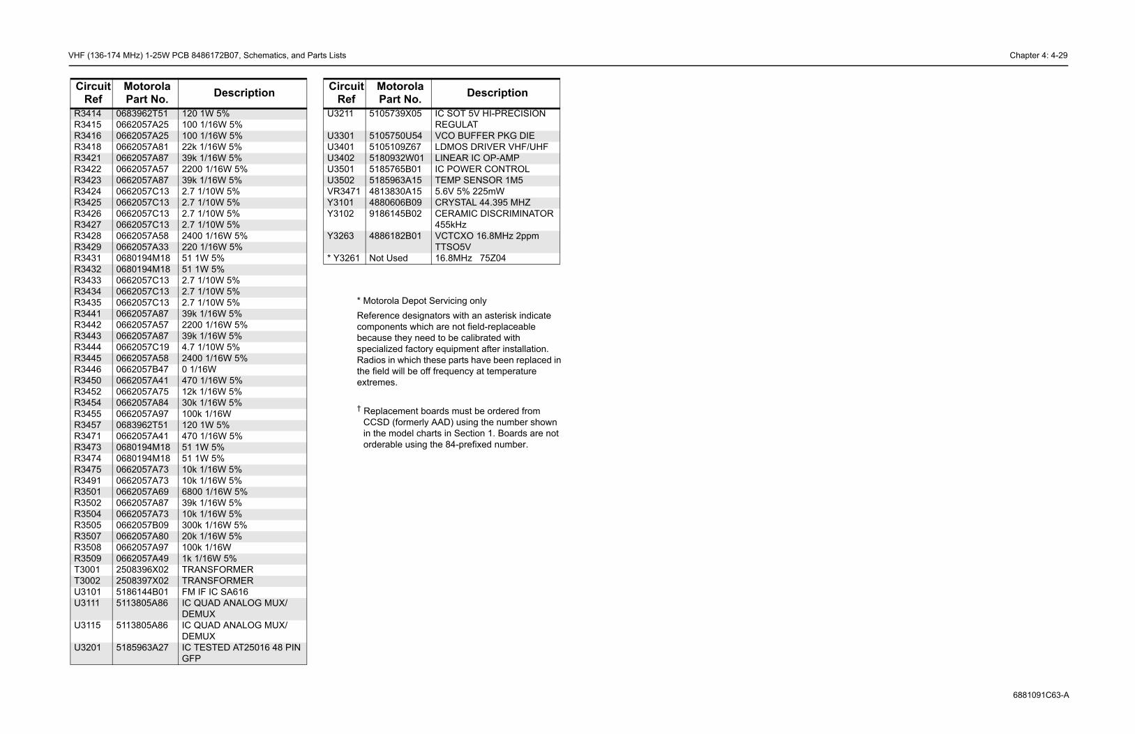
V Chapter 4: 4-29
6881091C63-A
HF (136-174 MHz) 1-25W PCB 8486172B07, Schematics, and Parts Lists
* Motorola Depot Servicing onlyReference designators with an asterisk indicate components which are not field-replaceable because they need to be calibrated with specialized factory equipment after installation. Radios in which these parts have been replaced in the field will be off frequency at temperature extremes.
† Replacement boards must be ordered from CCSD (formerly AAD) using the number shown in the model charts in Section 1. Boards are not orderable using the 84-prefixed number.
R3414 0683962T51 120 1W 5%R3415 0662057A25 100 1/16W 5%R3416 0662057A25 100 1/16W 5%R3418 0662057A81 22k 1/16W 5%R3421 0662057A87 39k 1/16W 5%R3422 0662057A57 2200 1/16W 5%R3423 0662057A87 39k 1/16W 5%R3424 0662057C13 2.7 1/10W 5%R3425 0662057C13 2.7 1/10W 5%R3426 0662057C13 2.7 1/10W 5%R3427 0662057C13 2.7 1/10W 5%R3428 0662057A58 2400 1/16W 5%R3429 0662057A33 220 1/16W 5%R3431 0680194M18 51 1W 5%R3432 0680194M18 51 1W 5%R3433 0662057C13 2.7 1/10W 5%R3434 0662057C13 2.7 1/10W 5%R3435 0662057C13 2.7 1/10W 5%R3441 0662057A87 39k 1/16W 5%R3442 0662057A57 2200 1/16W 5%R3443 0662057A87 39k 1/16W 5%R3444 0662057C19 4.7 1/10W 5%R3445 0662057A58 2400 1/16W 5%R3446 0662057B47 0 1/16WR3450 0662057A41 470 1/16W 5%R3452 0662057A75 12k 1/16W 5%R3454 0662057A84 30k 1/16W 5%R3455 0662057A97 100k 1/16WR3457 0683962T51 120 1W 5%R3471 0662057A41 470 1/16W 5%R3473 0680194M18 51 1W 5%R3474 0680194M18 51 1W 5%R3475 0662057A73 10k 1/16W 5%R3491 0662057A73 10k 1/16W 5%R3501 0662057A69 6800 1/16W 5%R3502 0662057A87 39k 1/16W 5%R3504 0662057A73 10k 1/16W 5%R3505 0662057B09 300k 1/16W 5%R3507 0662057A80 20k 1/16W 5%R3508 0662057A97 100k 1/16WR3509 0662057A49 1k 1/16W 5%T3001 2508396X02 TRANSFORMERT3002 2508397X02 TRANSFORMERU3101 5186144B01 FM IF IC SA616U3111 5113805A86 IC QUAD ANALOG MUX/
DEMUXU3115 5113805A86 IC QUAD ANALOG MUX/
DEMUXU3201 5185963A27 IC TESTED AT25016 48 PIN
GFP
Circuit Ref
Motorola Part No. Description
U3211 5105739X05 IC SOT 5V HI-PRECISION REGULAT
U3301 5105750U54 VCO BUFFER PKG DIEU3401 5105109Z67 LDMOS DRIVER VHF/UHFU3402 5180932W01 LINEAR IC OP-AMPU3501 5185765B01 IC POWER CONTROLU3502 5185963A15 TEMP SENSOR 1M5VR3471 4813830A15 5.6V 5% 225mWY3101 4880606B09 CRYSTAL 44.395 MHZY3102 9186145B02 CERAMIC DISCRIMINATOR
455kHzY3263 4886182B01 VCTCXO 16.8MHz 2ppm
TTSO5V* Y3261 Not Used 16.8MHz 75Z04
Circuit Ref
Motorola Part No. Description

Chapter 4: 4-30 VHF (136-174 MHz) 1-25W PCB 8486172B08, Schematics, and Parts Lists
6881091
5.0
C3002
C3
00
4
C3
00
5
C3
00
6
C3007
C3008
C3
00
9
C3010
C3011
C3
01
2
13
C3014
C3
01
5
C3
01
6
C3
01
7
C3
01
9
C3
02
0
C3027
C3
02
8
034
C3
10
2
C3
10
3
C3114
C3
11
5
C3124
C3
13
1
C3
13
2
C3133
C3
13
4
C3135
C3136
C3
13
7
C3
13
9
C3140
C3
14
1
C3
14
2
C3143
C3
14
5
C3
14
8
C3446
C3
44
7
C3472
C3473
C3
47
4
C3
49
7
D3001
D3003
D3004
D3
47
1
D3
47
2
2
56
FL3101
23
45
6
FL3102
2
FL3112
FL3114
2 3
J3401
L3
00
2
0
L3
10
1
L3
12
4L
34
71
L3472
L3493
Q3001
Q3
02
1
R3001R3002
R3003
R3
00
4
R3009
R3013
R3014
R3
01
5
R3
01
6
R3
02
4
R3025R3026
R3027
R3028
031
R3101
R3
10
6
R3
111
R3
11
7
R3
12
3
R3124
R3
13
0R
31
32
R3135
R3
14
2
R3144
R3
14
5
R3491
11
120
10
U3101
8 7
114
U3111
8 7
114
U31152
Y3102
1
1
1
WA
RIS
VH
F R
F B
oard
1-2
5W84
8617
2B08
-A T
OP
SID
EC
HE
CK
ON
E
O.K
. AS
IS
O.K
. AS
MA
RK
ED
(
)
(
)
ISS
.R
EV
ISIO
NR
LSE
.
CO
RR
EC
TE
DA
SM
AR
KE
D
ILLUSTRATOR
DATE
ENGINEER
DATE
PR
OG
RA
MD
ISK
RLS
E.
DW
G. N
O.
LET
TE
RIN
G S
IZE
:R
EQ
UIR
ES
:
EDITOR
DATE
CHECKER
DATE
Illus
trat
orR
K28
. Sep
. 200
0
ZW
G01
3059
1
O
ZW
G01
3059
1-O
VHF ZWG0130591-O
C63-A
VHF (136-174 MHz) 1-25W PCB 8486172B08, Schematics, and Parts Lists
C0101
C0
10
2
C0
10
4
C0
10
6
C0
10
7
C0
10
8
C0131
C0
13
2
C0
211
C0212
C0
22
1
C0
22
2
C0223
C0224
C0225
C0226
C0227
C0
22
8
C0
23
1
C0232
C0233
C0
23
4
C0235
C0236C0
23
7
C0241
C0242
C0243
C0244
C0245
C0246
C0251
C0252C0253
C0
25
6C
02
61
C0262
C0
42
1
C0
44
1
C0
44
2
C0
44
3
C0
44
5
C0
44
6
C0
44
7
C0
44
8
C0
44
9
C0
47
0
C0
47
1
C0
47
2
C0
47
3
C0
47
4
C0
47
6
C0
47
7
C0
47
8
C0
48
2
C0
48
3
C0484
C0
48
6
C0
48
7
C0
48
8
C0
49
0
C0
49
3
C0
49
4
C0
49
5
C0496
C0
50
1
C0
50
2
C0
50
3
C0
50
4
C0
50
5
C0
50
6
C0
50
8
C0
50
9
C0
51
0
C0
511
C0
51
2
C0
51
3
C0
51
4
C0
51
5
C0
51
6
C0
51
7
C0
51
8
C0542
C0601
C0603
C0
61
2
C0
65
1
C0
65
2
C0654
C0
65
5
C0681
C30
C3
01
8
C3021
C3032
C3
C3100
C3
10
1
C3210
C3211
C3212
C3213
C3
21
4
C3
21
5
C3
22
1
C3
22
2
C3
22
3
C3224
C3226
C3227
C3
22
9
C3231
C3
23
2
C3
23
3
C3
23
4
C3
24
0
C3242
C3243
C3244
C3245
C3246
C3247
C3
25
2
C3
25
3C
32
54
C3255
C3324
C3336
C3
33
7
C3341
C3
34
2
C3344
C3
34
5
C3
34
6
C3
34
7
C3357
C3361
C3
36
2
C3
36
3C
33
64
C3
36
5
C3400
C3401C3403
C3
40
4
C3
41
0
C3411C3412
C3417
C3418
C3419
C3420
C3
42
2 C3
42
3
C3
42
4
C3425
C3426
C3
42
8
C3
43
1
C3432
C3433
C3
43
4
C3
43
5
C3441C3442
C3443
C3444
C3
44
5
C3
44
8C
34
49
C3
45
3
C3
50
7
C3
50
8
C3509
D0201
D0
65
1
D3031
D3
22
1
D3
34
1
D3
36
1
D3
36
2
D3
40
1
3
4
4
3
181
J0451
2011
10
J0501
J0601
L0481
L0482
L3031
L3032
L3
03
4
L310
L3
20
1
L3232
L3333
L3341
L3343L3344
L3346
L3361
L3
36
2L
33
63
L3364
L3401
L3403
L3411L
34
12
L3413
L3414
L3422
L3
44
3
M3421
Q0110
Q0177Q0181
Q0185
Q0681
Q3
22
1
Q3304
Q3411
Q3422
2
3
4
5
6
7
8
Q3441Q
34
42
Q3
47
1
Q3472
R0101
R0102
R0
10
3
R0
10
4
R0105
R0106
R0
10
8
R0110
R0114
R0115
R0116
R0131
R0132
R0170
R0
18
1R
01
82
R0
18
5R
01
86
R0
211
R0212
R0220
R0221
R0222
R0
22
3
R0224
R0225
R0226
R0227
R0228
R0229
R0241
R0242
R0251
R0
25
2
R0
25
3
R0254
R0255
R0
25
6
R0257
R0261
R0
26
2R
02
68
R0
26
9
R0
44
2
R0510
R0
53
3
R0535
R0538
R0539
R0611R0
61
2
R0651
R0
65
2R0681
R0
68
2
R3
R3
20
2
R3211
R3221
R3
22
2
R3223
R3224
R3
22
5R3227
R3242
R3
25
1
R3
25
2
R3
33
5
R3
33
6
R3341
R3
34
2
R3361
R3362
R3
36
3
R3
36
4
R3400
R3401
R3
40
2
R3403
R3
40
4
R3
40
5
R3
40
6
R3414
R3415
R3416R
34
24
R3
42
5
R3
42
6
R3
42
7
R3
43
1
R3
43
2
R3433
R3434
R3435
R3471R3473
R3
50
5
R3
50
6
R3507
R3508
R3509
SH3301
3
4 6
12
T3001
3
46
1 2
T3002
TP
3401
1
7651
26
3217
16 1
87
1 14
U0211
1 37
2513
161
8 9
U0251
9
U0271
1
6
5
1
6
5
3
2
1
U3211
9
8
16
1
U3401
U3502
VR
05
01
VR0503
VR0505
VR0510
2 3
4
Y0
13
1
1
1
1
U0121Flashrom
U0101Microprocessor
U0221ASFIC CMP
U06515V Regulator
U06419,6V Regulator
U0611B+ Switch
(136-174 MHz) 1-25W PCB 8486172B08 Top Side
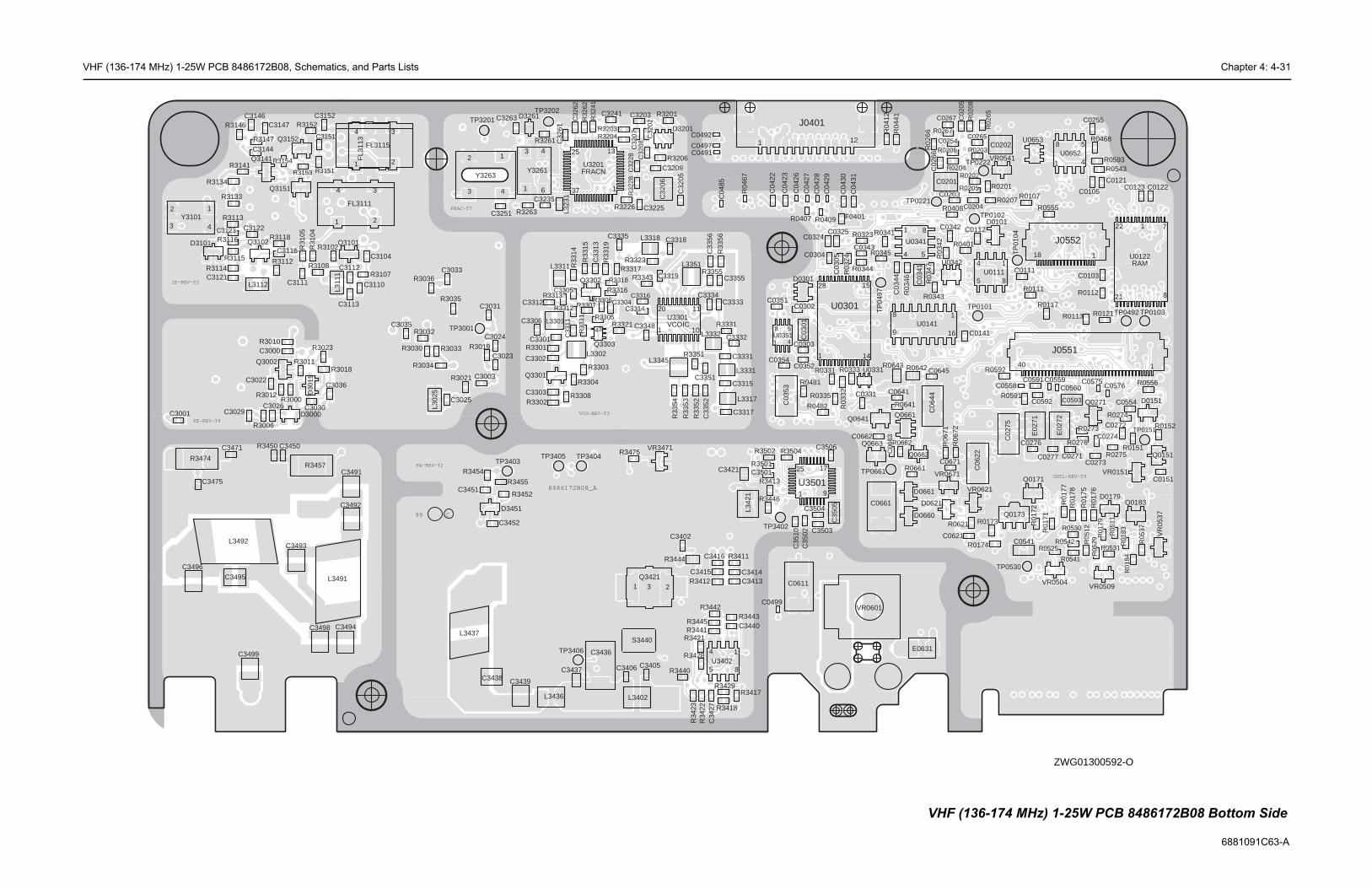
VHF (136-174 MHz) 1-25W PCB 8486172B08, Schematics, and Parts Lists Chapter 4: 4-31
6881091C63-A
C0103
C0105
C0111
C0112
C0121C0122C0123
C0141
C0151
C0201
C0202
C0203
C0204
C02
05
C0254
C0255
C0265
C02
66
C0267
C0271
C0272
C0273
C0274C02
75
C0276
C0277
C03
05
325
C0331
C03
41
C0342
C0343
C03
44
C04
30C
0431
C0541
C0554
C0558C0559
C0560C0575
C0576C0591
C0592 C0593
C0621
C06
22
C0641
C06
44
C0645
C0661
C0662
C06
63
C0671
C35
05
D0101
D0151
D0179D0621
D0660
D0661
E02
71
E02
72
E0631
F0401
12
140
J0551
118
J0552
Q0151
Q0171
Q0173
Q0183
Q0271
Q0641 Q0661
Q0662
Q0663
R0107
R0111 R0112
R0113
R0117R0121
R0151
R0152
R01
71
R01
72
R0173
R0174
R01
75R
0176
R01
77R
0178
R01
79
R01
83R
0184
R0201
R0202
R0203
R0204
R0205
R0206
R0207
R02
08
R02
65
R02
66
R0267
R0273
R0274
R0275
R0276
R0323
R03
24R
0332
R0333
R0341
R03
42
R0343
R0344
R0345
R03
46 R03
47
R0401
R0408
R04
12R
0441
R0468
R05
11
R05
12
R0525
R05
29
R0530
R0531
R05
37
R0541
R0542
R0543
R0555
R0556
R0591
R0592
R0593
R0621
R0641
R0642R0643
R0661
R0662 R06
71R
0672
TP0101
TP0102
TP0103
TP
0104
TP0151
TP0221
TP0222
TP0492TP
0497
TP0530
TP0661
14
5 8U0111
22
21 8
71
16
18
9U0141
15
14
0301
U0331
1
4 5
8
U0341
U0342
1 4
58U0652
U0653
VR0151
VR0504VR0509
VR
0537
VR0541
VR0601
VR0621
VR0671
U0122RAM
CNTL-REV-T9
ZWG01300592-O
VHF (136-174 MHz) 1-25W PCB 8486172B08 Bottom Side
C0301
C0302
C0303
C0304
C0324C0
C0351
C0352
C03
53
C0354
C04
22
C04
23
C04
26
C04
27C
0428
C04
29
C04
85
C0491
C0492
C0497
C0499
C0611
C3000
C3001
C3003C3022
C3023
C3024
C3025C3026
C3029C3030
C3031
C3033
C3035
C3036
C3104
C3110C3111
C3112
C3113
C3116
C3121
C3122C3123
C3144
C3146C3147
C3151
C3152
C32
02
C3203
C32
05
C32
06
C32
07C
3208
C3209
C3225
C32
28
C3235
C3241
C3251
C32
61
C32
62
C3263
C3301
C3302
C3303
C3304
C3305
C3306
C33
11
C3312
C33
13
C3314
C3315
C3316
C3317
C3318
C3319
C3331
C3332
C3333C3334
C3335
C3348
C3351
C33
52
C3355
C33
56
C3402
C3405C3406
C3413C3414C3415
C3416
C3421
C34
27
C3436
C3437C3438 C3439
C3440
C3450
C3451
C3452
C3471
C3475C3491
C3492
C3493
C3494
C3495
C3496
C3498
C3499
C3501
C35
02 C3503
C3504
C3506
C35
10
D0301
D3000
D30
11
D3101
D3201
D3261
D3451
4 3
2
FL3111
FL3
113
4 3
2
FL3115
J0401
L302
5
L311
1
L3112
L323
1
L3301
L3302
L3311
L3317
L3318
L3331
L3332
L3345
L3351
L3402
L342
1
L3436
L3437
L3491
L3492
Q3002
Q3101Q3102
Q3141
Q3151
Q3152
Q3301
Q3302
43
Q3303
1 23Q3421
R0331
R0335
R0407 R0409
R04
67
R0481
R0482R3000
R3006
R3010
R3011
R3012
R3018
R3019
R3021
R3023 R3030
R3032
R3033
R3034
R3035
R3036
R3102R31
04R
3105
R3107R3108
R3112
R3113
R3114
R3115
R3116 R3118
R3133
R3134
R3141
R3146
R3147
R3151
R3152
R3153
R3154
R3201
R3203R3204
R3206
R3226
R32
28
R32
41
R3261
R32
62
R3263
R3301
R3302
R3303
R3304
R3305
R3306R3307
R3308
R33
11
R3312
R3313
R33
14
R33
15
R3316
R3317
R3318
R33
19
R3321
R3323
R3331
R3343
R3351
R33
52
R33
53
R33
54
R3355
R33
56
R3411
R3412
R3413
R3417
R3418
R3421
R34
22R
3423
R3428
R3429
R3440
R3441
R3442R3443
R3444
R3445
R3446
R3450
R3452
R3454
R3455
R3457R3474
R3475
R3501
R3502 R3504
S3440
TP3001
TP3201TP3202
TP3402
TP3403TP3404TP3405
TP3406
28
1
U
4
58U0351
137
25 13
11
1
20
10
14
5 8U3402
1
17
9
25
U3501
VR3471
43
2Y3101
6
43
1
Y3261
2
3 4
Y3263
1
1
1
1
1
U3201FRACN
U3301VCOIC
8486172B08_A
C99
PA-REV-T2
VCO-REV-T3
IF-REV-T5
FE-REV-T4
FRAC-T7
1
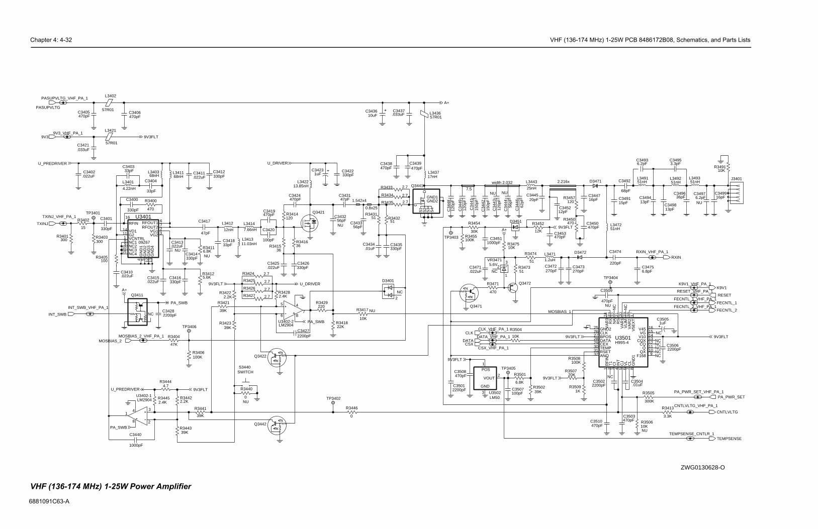
Chapter 4: 4-32 VHF (136-174 MHz) 1-25W PCB 8486172B08, Schematics, and Parts Lists
6881091
ZWG0130628-O
RXIN_VHF_PA_1
NU
NU
NU
NU
R350610K
120p
F
C34
44
6.2pF
C3509
th 2.032 2.216xJ3401
C35062200pF
R350239K
PASU
C3473270pF
10KR3491
100pFC3507
RESET_VHF_PA_1
C3504.01uF
470pFC3503
FECNTL_2
C35022200pF
25nH
L3443
10K
R3504
Q3472
RESET
IN
2
2
C3492
68pF
0
C34936.2pF
_PA_1
20pFC3445
1
13
C35051uF
6.8pFC3475
TEMPSENSETEMPSENSE_CNTLR_1
1K
R350720K
PA_PWR_SET
R3509
1F
C3495
C3497
3.3pF
C3474
220pF
TXIN
56pF
R3413
3.3K
9V3
FECNTL_2_VHF_PA_1
PA_1
D3472
C34
4662
pF
D3451
51nHL3493
R3474
51
R347351
C349115pF
D3471
L3471
1.2uH
51nH
R3508100K
L3491
R3505
300K
270pFC3472
C349636pF
C3510
CNTLVLTG_VHF_PA_1
470pF
PA_PWR_SET_VHF_PA_1
470pFC3453
R3501
L349251nH
6.8K
RXIN
13pFC3494
20V
AR
1
18V
AR
2
24V
AR
3
VG 15
6V
L19
VLI
M
TXINJ
21R
S
31 RSET
23R
X2
T1
30 TEMP
14V10
16V45
17V
5EX
T
9F168
8G
ND
1
25 GND2
4IN
T22
NA
11Q10QX
1R
FIN
29 CEX
3C
I
5C
J
7C
L
26 CLK
12CQCQX 1328 DATA H99S-4
U3501
32 ANO
27 BPOS
FECNTL_1_VHF_PA_1
16pFC3447
PA_1
470pF
R3452
12K
C349813pF
CNTLVLTG
16pFC3499
470pFC3450470
R3450
TP3405
PASUPV
10KR3475
R3457120
51nHL3472
12pFC3452
K9V1K9V1_VHF_PA_1
TP3404
FECNTL_1
9V3FLT
9V3FLTA+
NC
U_PRE
9V3FLT 9V3FLT
MOSBIAS_1
NC
NC
NC
NCNCNCNCNC
VHF (
C63-A
NU
NU
17nHL3437
NU
0
R3440
C3427
56pF
39K
10K
NU
6.8KR3411
NU
C3508
C34
43
1uFC3423
0.8x25
wid
1.542x4
7.5
R3427
R3426
2.7
2.7
2.7R3428
R3425
2.4K
120R3414
2.4K
MOSBIAS_2_VHF_PA_1
R3445
L3412
C3432
12nH
C3404
33pF
2200pF
C3410.022uF
PVLTG_VHF_PA_1
R341536
330pFC3426
Q3421
R3417
39K
R3443
R3441
C3416330pF
330pF
C3400 R3400
470
51R3432
.033uFC3437
L343657R01
470pFC3419
TP3402
TP3403
57R01
L3402
C3406470pF
R3401300
C3428
C3435
2200pF
C34
49
330pF
120p
F
470
R3471
C3434.01uF
MOSBIAS_247K
R3404
47pFC3431
C3421.033uF
CLK
51R3431
R3435 2.7
T_SWB
C3425.022uF
U3503
GND
POS1
VOUT
LM5
DATA_VHF
2.2KR3442
C3422330pF
R34444.7
5.6VVR347
2
39K
R3421
DATA
33pFC3403
C3451000p
.022uFC3471
CSX
6
5
78
4
J_VHF_PA_1
LM2904U3402-2
470pF
C35012200pF
INT_SWB_VHF_PA_1
D3401
CSX_VHF_
33pFC3418
L341168nH .022uF
C3411
R3403300
470pFC3405
100KR3406
11.03nH
5.6KR3412
L3413
120p
FC
3448
2.7R3424
47pF
C3417
C3439470pF
0
R3446
150p
FC
3442
R3455100K
10uFC3436
R3429220
R3433 2.7
C343356pF
22KR3418
2
31
8
4
C3440
1000pF
U3402-1LM2904
Q3442
R3402
15
39KR3423
Q3411
TP3406CLK_VHF_
TP3401
L342213.85nH
470pF
470pFC3424
30K
C3438
R3454
R3405100
330pF
C3401RFIN
16RFOUT1 6
RFOUT2 7
VCNTRL1
VD114 2VG1VG2 3
GN
D1
4
GN
D2
5
GN
D3
12G
ND
413
NC18NC29
NC310
NC415
09Z67
U3401
G211
LTG
36
L3403
R3416
Q3422
68nH 330pF
9V3_VHF_PA_1
C3412
SWITCHS3440
7.66nH
L3414
C3413.022uF
C34
4115
0pF
R3434 2.7
R34222.2K
Q3471
57R01
L3421
330pFC3414
D
G
GND1GND2
S1
S2
S3
S4
Q3441
.022uFC3415
100pF
C3420
C3402.022uF
NC
PA_SWB
A+
L3401
4.22nH
NC
U_DRIVER
9V3FLT
PA_SWB
U_DRIVER9V3FLT
9V3FLT
A+
U_PREDRIVER
NC
PA_SWB
9V3FLT
DRIVER
2
NU
136-174 MHz) 1-25W Power Amplifier

V Chapter 4: 4-33
6881091C63-A
9
G
G
G
20/25kHz 5VDC 12.5kHz 0VDC
9180469V04
9180468v04
9180468V06
0.1uFC3139
Q3141
1.8KR3142
R315410K
0.1uFC3142
0.1uFC3144
120pFC3143
14
VDD
7
VSS
U3115-2
5
CNTL
43
R31351.2K
BWSELECT_VHF_IF_1
10K
R3152
Q3152
C3152.01uF
Q3151
680
R3146
10K
R3151
VSS
7
C31400.1uF
MC
74
HC
40
66
U3111-4
TL
10VDD
14
5G
C31410.1uF
4700pFC3146
R3141390
2.4KR3144
FL3113CFUCJ455F
3
GN
D
1 IN 2OUT
CNTL
13
12 VDD
14
VSS
7
DISCAUDIO_VHF_IF_1
MC
74
HC
40
66
U3115-1
R3147
12K
455KHz3
BWSELECT
45B02
Y3102
MC
74
HC
40
66
6
CNTL
14
VDD
7
VSS
U3115-3
DISCAUDIO
3.3K
R3145
C31470.1uF
0.1uFC3145
RSSI_VHF_IF_1
C3151.01uF
14
VDD
7
VSS
RSSI
U3111-3
MC
74
HC
40
66
TL
FL3114CFUCJ455D
3G
ND
1 IN 2OUT
CNTL
12
11 10VDD
14
VSS
7
MC
74
HC
40
66
U3115-4
11
LIM
OU
T1
3L
IM_
DE
C1
12
LIM
_D
EC
2
10
QU
AD
IN
AU
DIO
OU
TA
UD
IO_
FE
ED
GND15
18
IFA
MP
IN1
6IF
AM
PO
UT
19
IFA
MP
_D
EC
11
7IF
AM
P_
DE
C2
14
LIM
IN
10KR3153
220pFC3148
NU
D
OUT 2
CFWC455FFL3115
GN
D1
3 4G
ND
2
IN1NU
9V3
9V3
9V3
5V
1
2
9 8
VHF (136-174 MHz) 1-25W IF
ZWG0130565-B
HF (136-174 MHz) 1-25W PCB 8486172B08, Schematics, and Parts Lists
G
G
G
4802245J84
NOTPLACED 2113740L30 33pF
L3124
9180469V03
0.75VDC 0.75VDC
3VDC
NOTPLACED
2113740F35 22pF
Y3101 4880606B09
3.9VDC
fundamental xtal 3rd overtone xtal
R3123 0662057B47 0 NOTPLACED
R3124 NOTPLACED 0662057A49 1K
C3124
2462587N68 1uH
C3136 2113740L29 30pF
9180469V06
3VDC
VDD
14
VSS
7
MC
74
HC
40
66
U3111-1
CNTL
13
12
R3116330
82pFC3112
10R3112
C3110
27pF
15KR3132
390
GN
D2
2
GN
D3
4 5G
ND
4
3IN
6OUT
R3115
FL310112R16
1G
ND
1
R3117
27K
IF
Q3102IFIN_VHF_IF_1
R3104
NU
C31139.1pF
NU100
620nHL3111
620R3108
6.8K
R3107
C3103
33pF
C31320.1uF
R3118
6.8K
R311112K
5V_VHF_IF_1
CN
12
11
C3101
3G
ND
1
GN
D2
4
1 IN 2OUT
NU2.2pF
FL3111CFWC45
R31338.2K
R3106
27K
VDD
7
VSS
U3111-2
MC
74
HC
40
66
5
CNTL
43
14
1pFC3131
C3122
.039uF
NU
R310210
9V3_VHF_IF_2
12KR3101
C313310uF
R3105
22pF
C3115
L3100
100
0.1uF
9V3
NU620nH
C3137.039uF
C3134
5V
D3101
0.1uFC3111
GN
D3
GN
D4
5
IN3
OUT6
12R16FL3102
GN
D1
1 2G
ND
24
C3100
1000pF620nHL3101
C3123.039uF
2G
ND
4G
ND
1
3OUT
1IN
R3130
51
44.395MHz
45J84Y3101
33pF
C3136
C3135
6
CN
0.1uF
C3116
0.1uFC3121
Q3101
2R
FIN
_D
EC
5R
SS
IOU
T9
RS
SI_
FE
ED
6VCC
330R3113
20
MIX
OU
T
4O
SC
IN3
OS
CO
UT
1R
FIN
87
SA616U3101
C3104
0.1uF
620nH
9V3_VHF_IF_1
L3112
R3123
L3124
C3124
*R3124
C311418pF
4
1 IN 2OUT
FL3112CFWC455
3G
ND
1
GN
D2
NU
R3114100
R3134
10K
15pFC3102 5V
5V
9V3
9V39V3
5V
9V3
8
*
*
*
*
*
*
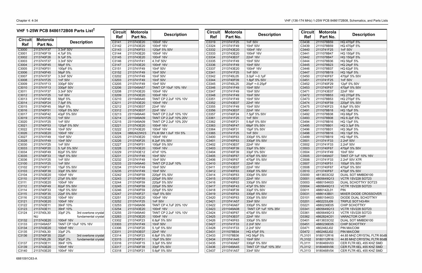
Chapter 4: 4-34 VHF (136-174 MHz) 1-25W PCB 8486172B08, Schematics, and Parts Lists
688109
VHF 1 †
CircRe
C3000C3001C3002C3003C3004C3005C3006C3007C3008C3009C3010C3011C3012C3013C3014C3015C3016C3017C3019C3020C3021C3022C3026C3027C3028C3030C3033C3034C3035C3036C3100C3102C3103C3104C3110C3111C3112C3114C3115C3116C3121C3122C3123C3124
C3132C3133C3134C3135C3136
C3137C3139C3140
V6V6VVVV6V
-0.1pF% 50V0.25pFVVVVVVV
% 50V
% 50V 50V 50V
% 50V% 50VV 50V 50V
% 50V% 50VVV% 50V% 50VV% 50V 50V 50V
% 50V% 50VV% 50VP 1uF 10% 35V% 50VV% 50V
0V0VF 5%F 5%V% 50VP 10uF 10% 35VV
DescriptionC3438 2111078B59 HQ 470pF 5%C3439 2111078B59 HQ 470pF 5%C3440 2113741F25 1nF 50VC3441 2111078B47 HQ 150pF 5%C3442 2111078B47 HQ 150pF 5%C3444 2111078B36 HQ 56pF 5%C3445 2111078B23 HQ 24pF 5%C3446 2111078B37 HQ 62pF 5%C3447 2111078B19 HQ 16pF 5%C3450 2113740F67 470pF 5% 50VC3451 2113741F25 1nF 50VC3452 2113740F29 12pF 5% 50VC3453 2113740F67 470pF 5% 50VC3471 2113743E07 22nF 16VC3472 2111078B53 HQ 270pF 5%C3473 2111078B53 HQ 270pF 5%C3474 2113740F59 220pF 5% 50VC3475 2113740F23 6.8pF 5% 50VC3491 2111078B18 HQ 15pF 5%C3492 2111078B38 HQ 68pF 5%C3493 2111078B08 HQ 6.2pF 5%C3494 2111078B16 HQ 13pF 5%C3495 2111078B01 HQ 3.3pF 5%C3496 2111078B31 HQ 36pF 5%C3498 2111078B16 HQ 13pF 5%C3499 2111078B19 HQ 16pF 5%C3501 2113741F33 2.2nF 50VC3502 2113741F33 2.2nF 50VC3503 2113740F67 470pF 5% 50VC3504 2113741F49 10nF 50VC3505 2311049A07 TANT CP 1uF 10% 16VC3506 2113741F33 2.2nF 50V X7RC3507 2113740F51 100pF 5% 50VC3508 2113740F67 470pF 5% 50VC3510 2113740F67 470pF 5% 50VD3000 4813833C02 DUAL SOT MMBD6100D3001 4805649Q13 VCTR 1SV228 SOT23D3003 4880154K03 DUAL SCHOTTKY SOT23D3004 4805649Q13 VCTR 1SV228 SOT23D3011 4880142L01 PIND3031 4886143B01 MIXER DIODE CROSSOVERD3101 4880154K03 DIODE DUAL SCHOTTKYD3201 4802233J09 TRIPLE SOT143-RHD3221 4880236E05 CHIP SCHOTTKYD3341 4805649Q13 VCTR 1SV228 SOT23D3361 4805649Q13 VCTR 1SV228 SOT23D3362 4862824C01 VARACTOR CHIPD3401 4813833C02 DUAL SOT MMBD6100D3451 4880236E05 CHIP SCHOTTKYD3471 4802482J02 PIN MA/COMD3472 4802482J02 PIN MA/COMFL3101 9180112R16 44.85 MHZ CRYSTAL FLTR 80dBFL3102 9180112R16 44.85 MHZ CRYSTAL FLTR 80dBFL3111 9180469V03 CER FLTR 6EL 455 KHZ SMDFL3112 9180469V06 CER FLTR 6EL 455 KHZ SMDFL3113 9180468V04 CER FLTR 4EL 455 KHZ SMD
Circuit Ref
Motorola Part No. Description
1C63-A
-25W PCB 8486172B08 Parts List
uit f
Motorola Part No. Description
2113741F37 3.3nF 50V2113740F19 4.7pF 5%2113740F26 9.1pF 5%2113741F37 3.3nF 50V2113740F45 56pF 5%2113740F51 100pF 5%2113740F45 56pF 5%2113741F37 3.3nF 50V2113741F25 1nF 50V2113741F13 330pF 50V2113741F13 330pF 50V2113741F37 3.3nF 50V2113741F25 1nF 50V2113740F45 56pF 5%2113740F24 7.5pF 5%2113740F45 56pF 5%2113740F51 100pF 5% 50V2113740F42 43pF 5% 50V2113741F25 1nF 50V2113741F25 1nF 50V2113740F53 120pF 5% 50V2113741F49 10nF 50V2113743E20 100nF 16V2113741F49 10nF 50V2113741F49 10nF 50V2113741F25 1nF 50V2113740F20 5.1pF 5% 50V2113740F49 82pF 5% 50V2113740F33 18pF 5% 50V2113741F25 1nF 50V2113741F25 1nF 50V2113740F31 15pF 5% 50V2113740F39 33pF 5% 50V2113743E20 100nF 16V2113740F37 27pF 5% 50V2113743E20 100nF 16V2113740F49 82pF 5% 50V2113740F33 18pF 5% 50V2113740F35 22pF 5% 50V2113743E20 100nF 16V2113743E20 100nF 16V2113743E11 39nF 10%2113743E11 39nF 10%2113740L30NU
33pF 2% 3rd overtone crystalfundamental crystal
2113743E20 100nF 16V2311049A57 TANT CP 10uF 10% 16V2113743E20 100nF 16V2113740L30 33pF 2%2113740F352113740L29
22pF 3rd overtone crystal30pF 2% fundamental crystal
2113743E11 39nF 10%2113743E20 100nF 16V2113743E20 100nF 16V
C3141 2113743E20 100nF 16VC3142 2113743E20 100nF 16VC3143 2113740F53 120pF 5% 50VC3144 2113743E20 100nF 16VC3145 2113743E20 100nF 16VC3146 2113741F41 4.7nF 50VC3147 2113743E20 100nF 16VC3151 2113741F49 10nF 50VC3152 2113741F49 10nF 50VC3202 2113741F49 10nF 50VC3203 2113741F49 10nF 50VC3205 2113741F49 10nF 50VC3206 2311049A57 TANT CP 10uF 10% 16VC3208 2113743E20 100nF 16VC3209 2113743E20 100nF 16VC3210 2311049A40 TANT CP 2.2uF 10% 10VC3211 2113743E20 100nF 16VC3212 2113743E07 22nF 16VC3312 2113743E07 22nF 16VC3213 2311049A40 TANT CP 2.2uF 10% 10VC3214 2311049A09 TANT CP 2.2uF 10% 20VC3215 2311049A09 TANT CP 2.2uF 10% 20VC3221 2113743E20 100nF 16VC3222 2113743E20 100nF 16VC3224 0882422W23 FILM SM 1.0uF 15V 5%C3225 2113743E20 100nF 16VC3226 2113740F25 8.2pF 5% 50VC3227 2113740F51 100pF 5% 50VC3228 2113743E20 100nF 16VC3229 2113743E12 47nF 10%C3231 2113741F49 10nF 50VC3232 2113741F49 10nF 50VC3233 2311049A40 TANT CP 2.2uF 10%C3234 2113741F49 10nF 50VC3235 2113741F49 10nF 50VC3242 2113740F59 220pF 5% 50VC3243 2113740F59 220pF 5% 50VC3244 2113740F59 220pF 5% 50VC3245 2113740F59 220pF 5% 50VC3246 2113740F59 220pF 5% 50VC3247 2113740F27 10pF 5% 50VC3251 2113743E20 100nF 16VC3252 2113741F25 1nF 50VC3253 2311049A56 TANT CP 4.7uF 20% 10VC3254 2113743E20 100nF 16VC3255 2311049A40 TANT CP 2.2uF 10% 10VC3263 2113743E20 100nF 16VC3302 2113740F23 6.8pF 5% 50VC3303 2113741F49 10nF 50VC3306 2113740F20 5.1pF 5% 50VC3311 2113743E07 22nF 16VC3314 2113740F23 6.8pF 5% 50VC3315 2113740F31 15pF 5% 50VC3316 2113740F15 3.3pF 5% 50VC3317 2113740F39 33pF 5% 50VC3318 2113740F21 5.6pF 5% 50V
Circuit Ref
Motorola Part No. Description
C3319 2113741F25 1nF 50VC3324 2113741F49 10nF 50C3332 2113743E20 100nF 1C3333 2113743E20 100nF 1C3334 2113743E07 22nF 16C3335 2113741F49 10nF 50C3336 2113741F49 10nF 50C3337 2113743E20 100nF 1C3341 2113741F25 1nF 50VC3342 2113740L05 3.0pF +C3344 2113740F09 1.8pF 5C3345 2113740L25 20pF +-C3346 2113741F49 10nF 50C3347 2113741F49 10nF 50C3348 2113741F49 10nF 50C3351 2113741F49 10nF 50C3352 2113743E07 22nF 16C3355 2113741F49 10nF 50C3356 2113743E07 22nF 16C3357 2113740F24 7.5pF 5C3361 2113741F25 1nF 50VC3362 2113740F21 5.6pF 5C3363 2113740F47 68pF 5%C3364 2113740F31 15pF 5%C3365 2113741F25 1nF 50VC3400 2113740F63 330pF 5C3401 2113740F63 330pF 5C3402 2113743E07 22nF 16C3403 2113740F39 33pF 5%C3404 2113740F39 33pF 5%C3405 2113740F67 470pF 5C3406 2113740F67 470pF 5C3410 2113743E07 22nF 16C3411 2113743E07 22nF 16C3412 2113740F63 330pF 5C3414 2113740F63 330pF 5C3415 2113743E07 22nF 16C3416 2113740F63 330pF 5C3417 2113740F43 47pF 5%C3418 2113740F39 33pF 5%C3419 2113740F63 330pF 5C3420 2113740F63 330pF 5C3421 2113741A57 33nF 50C3422 2113740A67 330pF 5C3423 2311049A08 TANT CC3424 2113740F67 470pF 5C3425 2113743E07 22nF 16C3426 2113740F63 330pF 5C3427 2113741F33 2.2nF 5C3428 2113741F33 2.2nF 5C3431 2111078B34 HQ 47pC3433 2111078B36 HQ 56pC3434 2113741A45 10nF 50C3435 2113740A67 330pF 5C3436 2311049A45 TANT CC3437 2113741A57 33nF 50
Circuit Ref
Motorola Part No.
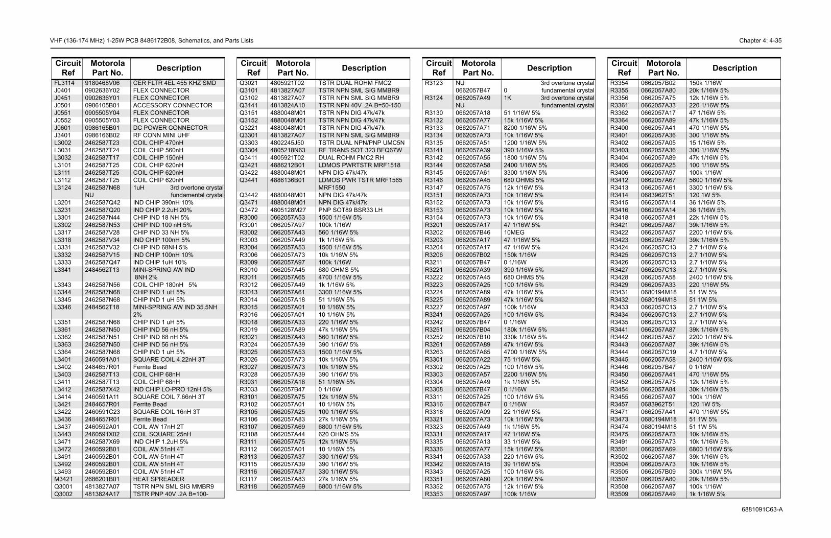
V Chapter 4: 4-35
6881091C63-A
3rd overtone crystalfundamental crystal
K 3rd overtone crystalfundamental crystal
1 1/16W 5%5k 1/16W 5%200 1/16W 5%0k 1/16W 5%200 1/16W 5%90 1/16W 5%800 1/16W 5%400 1/16W 5%300 1/16W 5%80 OHMS 5%2k 1/16W 5%0k 1/16W 5%0k 1/16W 5%0k 1/16W 5%0k 1/16W 5%7 1/16W 5%0MEG7 1/16W 5%7 1/16W 5%50k 1/16W 1/16W90 1/16W 5%80 OHMS 5%00 1/16W 5%7k 1/16W 5%7k 1/16W 5%00k 1/16W00 1/16W 5% 1/16W80k 1/16W 5%30k 1/16W 5%7k 1/16W 5%700 1/16W 5%5 1/16W 5%00 1/16W 5%200 1/16W 5%k 1/16W 5% 1/16W00 1/16W 5% 1/16W2 1/16W 5%0k 1/16W 5%k 1/16W 5%7 1/16W 5%3 1/16W 5%5k 1/16W 5%20 1/16W 5%9 1/16W 5%00 1/16W 5%0k 1/16W 5%2k 1/16W 5%00k 1/16W
DescriptionR3354 0662057B02 150k 1/16WR3355 0662057A80 20k 1/16W 5%R3356 0662057A75 12k 1/16W 5%R3361 0662057A33 220 1/16W 5%R3362 0662057A17 47 1/16W 5%R3364 0662057A89 47k 1/16W 5%R3400 0662057A41 470 1/16W 5%R3401 0662057A36 300 1/16W 5%R3402 0662057A05 15 1/16W 5%R3403 0662057A36 300 1/16W 5%R3404 0662057A89 47k 1/16W 5%R3405 0662057A25 100 1/16W 5%R3406 0662057A97 100k 1/16WR3412 0662057A67 5600 1/16W 5%R3413 0662057A61 3300 1/16W 5%R3414 0683962T51 120 1W 5%R3415 0662057A14 36 1/16W 5%R3416 0662057A14 36 1/16W 5%R3418 0662057A81 22k 1/16W 5%R3421 0662057A87 39k 1/16W 5%R3422 0662057A57 2200 1/16W 5%R3423 0662057A87 39k 1/16W 5%R3424 0662057C13 2.7 1/10W 5%R3425 0662057C13 2.7 1/10W 5%R3426 0662057C13 2.7 1/10W 5%R3427 0662057C13 2.7 1/10W 5%R3428 0662057A58 2400 1/16W 5%R3429 0662057A33 220 1/16W 5%R3431 0680194M18 51 1W 5%R3432 0680194M18 51 1W 5%R3433 0662057C13 2.7 1/10W 5%R3434 0662057C13 2.7 1/10W 5%R3435 0662057C13 2.7 1/10W 5%R3441 0662057A87 39k 1/16W 5%R3442 0662057A57 2200 1/16W 5%R3443 0662057A87 39k 1/16W 5%R3444 0662057C19 4.7 1/10W 5%R3445 0662057A58 2400 1/16W 5%R3446 0662057B47 0 1/16WR3450 0662057A41 470 1/16W 5%R3452 0662057A75 12k 1/16W 5%R3454 0662057A84 30k 1/16W 5%R3455 0662057A97 100k 1/16WR3457 0683962T51 120 1W 5%R3471 0662057A41 470 1/16W 5%R3473 0680194M18 51 1W 5%R3474 0680194M18 51 1W 5%R3475 0662057A73 10k 1/16W 5%R3491 0662057A73 10k 1/16W 5%R3501 0662057A69 6800 1/16W 5%R3502 0662057A87 39k 1/16W 5%R3504 0662057A73 10k 1/16W 5%R3505 0662057B09 300k 1/16W 5%R3507 0662057A80 20k 1/16W 5%R3508 0662057A97 100k 1/16WR3509 0662057A49 1k 1/16W 5%
Circuit Ref
Motorola Part No. Description
HF (136-174 MHz) 1-25W PCB 8486172B08, Schematics, and Parts Lists
FL3114 9180468V06 CER FLTR 4EL 455 KHZ SMDJ0401 0902636Y02 FLEX CONNECTORJ0451 0902636Y01 FLEX CONNECTORJ0501 0986105B01 ACCESSORY CONNECTORJ0551 0905505Y04 FLEX CONNECTORJ0552 0905505Y03 FLEX CONNECTORJ0601 0986165B01 DC POWER CONNECTORJ3401 0986166B02 RF CONN MINI UHFL3002 2462587T23 COIL CHIP 470nHL3031 2462587T24 COIL CHIP 560nHL3032 2462587T17 COIL CHIP 150nHL3101 2462587T25 COIL CHIP 620nHL3111 2462587T25 COIL CHIP 620nHL3112 2462587T25 COIL CHIP 620nHL3124 2462587N68
NU1uH 3rd overtone crystal
fundamental crystalL3201 2462587Q42 IND CHIP 390nH 10%L3231 2462587Q20 IND CHIP 2.2uH 20%L3301 2462587N44 CHIP IND 18 NH 5%L3302 2462587N53 CHIP IND 100 nH 5%L3317 2462587V28 CHIP IND 33 NH 5%L3318 2462587V34 IND CHIP 100nH 5%L3331 2462587V32 CHIP IND 68NH 5%L3332 2462587V15 IND CHIP 100nH 10%L3333 2462587Q47 IND CHIP 1uH 10%L3341 2484562T13 MINI-SPRING AW IND
8NH 2%L3343 2462587N56 COIL CHIP 180nH 5%L3344 2462587N68 CHIP IND 1 uH 5%L3345 2462587N68 CHIP IND 1 uH 5%L3346 2484562T18 MINI-SPRING AW IND 35.5NH
2%L3351 2462587N68 CHIP IND 1 uH 5%L3361 2462587N50 CHIP IND 56 nH 5%L3362 2462587N51 CHIP IND 68 nH 5%L3363 2462587N50 CHIP IND 56 nH 5%L3364 2462587N68 CHIP IND 1 uH 5%L3401 2460591A01 SQUARE COIL 4.22nH 3TL3402 2484657R01 Ferrite BeadL3403 2462587T13 COIL CHIP 68nHL3411 2462587T13 COIL CHIP 68nHL3412 2462587X42 IND CHIP LO-PRO 12nH 5%L3414 2460591A11 SQUARE COIL 7.66nH 3TL3421 2484657R01 Ferrite BeadL3422 2460591C23 SQUARE COIL 16nH 3TL3436 2484657R01 Ferrite BeadL3437 2460592A01 COIL AW 17nH 2TL3443 2460591X02 COIL SQUARE 25nHL3471 2462587X69 IND CHIP 1.2uH 5%L3472 2460592B01 COIL AW 51nH 4TL3491 2460592B01 COIL AW 51nH 4TL3492 2460592B01 COIL AW 51nH 4TL3493 2460592B01 COIL AW 51nH 4TM3421 2686201B01 HEAT SPREADERQ3001 4813827A07 TSTR NPN SML SIG MMBR9Q3002 4813824A17 TSTR PNP 40V .2A B=100-
Circuit Ref
Motorola Part No. Description
Q3021 4805921T02 TSTR DUAL ROHM FMC2Q3101 4813827A07 TSTR NPN SML SIG MMBR9Q3102 4813827A07 TSTR NPN SML SIG MMBR9Q3141 4813824A10 TSTR NPN 40V .2A B=50-150Q3151 4880048M01 TSTR NPN DIG 47k/47kQ3152 4880048M01 TSTR NPN DIG 47k/47kQ3221 4880048M01 TSTR NPN DIG 47k/47kQ3301 4813827A07 TSTR NPN SML SIG MMBR9Q3303 4802245J50 TSTR DUAL NPN/PNP UMC5NQ3304 4805218N63 RF TRANS SOT 323 BFQ67WQ3411 4805921T02 DUAL ROHM FMC2 RHQ3421 4886212B01 LDMOS PWRTSTR MRF1518Q3422 4880048M01 NPN DIG 47k/47kQ3441 4886136B01 LDMOS PWR TSTR MRF1565
MRF1550Q3442 4880048M01 NPN DIG 47k/47kQ3471 4880048M01 NPN DIG 47k/47kQ3472 4805128M27 PNP SOT89 BSR33 LHR3000 0662057A53 1500 1/16W 5%R3001 0662057A97 100k 1/16WR3002 0662057A43 560 1/16W 5%R3003 0662057A49 1k 1/16W 5%R3004 0662057A53 1500 1/16W 5%R3006 0662057A73 10k 1/16W 5%R3009 0662057A97 100k 1/16WR3010 0662057A45 680 OHMS 5%R3011 0662057A65 4700 1/16W 5%R3012 0662057A49 1k 1/16W 5%R3013 0662057A61 3300 1/16W 5%R3014 0662057A18 51 1/16W 5%R3015 0662057A01 10 1/16W 5%R3016 0662057A01 10 1/16W 5%R3018 0662057A33 220 1/16W 5%R3019 0662057A89 47k 1/16W 5%R3021 0662057A43 560 1/16W 5%R3024 0662057A39 390 1/16W 5%R3025 0662057A53 1500 1/16W 5%R3026 0662057A73 10k 1/16W 5%R3027 0662057A73 10k 1/16W 5%R3028 0662057A39 390 1/16W 5%R3031 0662057A18 51 1/16W 5%R3033 0662057B47 0 1/16W R3101 0662057A75 12k 1/16W 5%R3102 0662057A01 10 1/16W 5%R3105 0662057A25 100 1/16W 5%R3106 0662057A83 27k 1/16W 5%R3107 0662057A69 6800 1/16W 5%R3108 0662057A44 620 OHMS 5%R3111 0662057A75 12k 1/16W 5% R3112 0662057A01 10 1/16W 5%R3113 0662057A37 330 1/16W 5%R3115 0662057A39 390 1/16W 5%R3116 0662057A37 330 1/16W 5%R3117 0662057A83 27k 1/16W 5%R3118 0662057A69 6800 1/16W 5%
Circuit Ref
Motorola Part No. Description
R3123 NU0662057B47 0
R3124 0662057A49NU
1
R3130 0662057A18 5R3132 0662057A77 1R3133 0662057A71 8R3134 0662057A73 1R3135 0662057A51 1R3141 0662057A39 3R3142 0662057A55 1R3144 0662057A58 2R3145 0662057A61 3R3146 0662057A45 6R3147 0662057A75 1R3151 0662057A73 1R3152 0662057A73 1R3153 0662057A73 1R3154 0662057A73 1R3201 0662057A17 4R3202 0662057B46 1R3203 0662057A17 4R3204 0662057A17 4R3206 0662057B02 1R3211 0662057B47 0R3221 0662057A39 3R3222 0662057A45 6R3223 0662057A25 1R3224 0662057A89 4R3225 0662057A89 4R3227 0662057A97 1R3241 0662057A25 1R3242 0662057B47 0R3251 0662057B04 1R3252 0662057B10 3R3261 0662057A89 4R3263 0662057A65 4R3301 0662057A22 7R3302 0662057A25 1R3303 0662057A57 2R3304 0662057A49 1R3308 0662057B47 0R3311 0662057A25 1R3316 0662057B47 0R3318 0662057A09 2R3321 0662057A73 1R3323 0662057A49 1R3331 0662057A17 4R3335 0662057A13 3R3336 0662057A77 1R3341 0662057A33 2R3342 0662057A15 3R3343 0662057A25 1R3351 0662057A80 2R3352 0662057A75 1R3353 0662057A97 1
Circuit Ref
Motorola Part No.

Chapter 4: 4-36 VHF (136-174 MHz) 1-25W PCB 8486172B08, Schematics, and Parts Lists
688109
T3001T3002U3101U3111U3115U3201
U3211
U3301U3401
U3402U3501U3502VR347Y3101
Y3102
Y3263
* Y326
CircRe
1C63-A
* Motorola Depot Servicing onlyReference designators with an asterisk indicate components which are not field-replaceable because they need to be calibrated with specialized factory equipment after installation. Radios in which these parts have been replaced in the field will be off frequency at temperature extremes.
† Replacement boards must be ordered from CCSD (formerly AAD) using the number shown in the model charts in Section 1. Boards are not orderable using the 84-prefixed number.
2508396X02 TRANSFORMER2508397X02 TRANSFORMER5186144B01 FM IF IC SA6165113805A86 IC QUAD ANALOG MUX/DEMUX5113805A86 IC QUAD ANALOG MUX/DEMUX5185963A27 IC TESTED AT25016 48 PIN
GFP5105739X05 IC SOT 5V HI-PRECISION REG-
ULAT5105750U54 VCO BUFFER PKG DIE5185130C65 LDMOS DRIVER VHF/UHF/
800MHz5180932W01 LINEAR IC OP-AMP5185765B01 IC POWER CONTROL5185963A15 TEMP SENSOR 1M5
1 4813830A15 5.6V 5% 225mW
4802245J844880606B09
2ND OSC XTAL 44.395 MHZ3rd overtone crystalfundamental crystal
9186145B02 CERAMIC DISCRIMINATOR 455kHz
4886182B01 VCTCXO 16.8MHz 2ppm TTSO5V
1 Not Used 16.8MHz 75Z04
uit f
Motorola Part No. Description