
Availability Performance of LCLS X-Ray FEL at SLAC William Colocho for the LCLS team.
Project Title: FLORA: A 3D-Integrated CMOS Detector for Imaging Experiments at LCLS-II
Applicants/Institutions: SLAC National Accelerator Laboratory, FermilabPrincipal Investigators: Gabriella Carini, Grzegorz Deptuch, Farah Fahim
Project Summary
The SLAC Linac Coherent Light Source (LCLS) is the world’s first hard X-ray free electron laser. It opened the door to revolutionary experiments in atomic and molecular dynamics. A major upgrade (LCLS-II) is now underway. A 4 GeV superconducting electron linear accelerator will be installed in the LCLS tunnel. An increase in the repetition rate from 120 to 1 million pulses per second will be enabled.In order to take advantage of the new capabilities of LCLS-II, a new generation of photon imaging detectors needs to be developed. Currently available detectors for soft X-ray imaging are still scientific CCDs, with limited dynamic range and frame readout rate. We propose to develop a novel detector, FLORA (Fermilab-LCLS CMOS 3D-integRated detector with Autogain), with very low noise, high dynamic range and fast readout suitable for imaging experiments at the upcoming LCLS-II. Specifically:
Small pixel size (~50 m x 50 m pixels) Frame readout > 10 kfps (with path towards higher effective readout speed) Possessing built-in adaptive gain, leading to handling up to 1,000 photons
per pixel per frame with a single photon resolution High quantum efficiency in the energy range between 250 eV and 2 keV Tileable to cover large areas (solid angle).
This major leap in detector and readout electronics we envision is based on recent advances in CMOS sensors and 3D integration. The concept here presented can be implemented in detectors for various photon energies, however the priority, set by the upcoming LCLS-II, is given to the soft x-ray range.
During the R&D phase, here proposed, we will have to tackle several aspects in parallel such as CMOS sensor, readout ASIC, 3D assembly, testing, etc.
One of the key components of the project is the CMOS sensor: although several parts have been separately demonstrated elsewhere, they have never been implemented all together in a single sensor. For this challenging part we plan to take advantage of our industry liaison. The readout ASIC and 3D assembly will leverage the unique expertise of the team. Testing will be performed with lab x-ray sources and at SLAC users facilities.
Budget Justification
This budget was developed for a 2-year period of performance starting on 07/01/2016 and ending on 06/30/2018. Inflation is estimated at 2.5% for materials and services. The activities in this proposal will be performed at SLAC National Accelerator Laboratory which is funded by the Department of Energy (DOE) through a Management and Operating (M&O) contract with Stanford University. Under the M&O contract, SLAC is required to follow the DOE policies and guidance on direct and indirect cost allocation.
This proposal does not include funding for SLAC labor. Any required support will be provided by SLAC LCLS Directorate.
Materials & Supplies:The total unburdened cost of M&S is $540,995, which is comprised of $213,200 in FY17 and $327,795 in FY18, and covers the fabrication of test structures and small sensor prototypes in CMOS sensor in “opto” process. The estimate is based on experience with similar work and information from the CMOS effort ongoing in the high-energy community. It also covers the service for the soft x-ray entrance window.
Consultant Services:We are including costs associated with external consulting services of $123,778 of direct cost performed across 24 months. The estimate is based on typical foundry charges for non-recurring engineering (NRE) consultation required in case of new technology development.
Summary of Direct Costs, including inflation:Total Direct Cost is $ 664,773: $15,000 in FY16, $274,700 in FY17, $375,073 in FY18.
Indirect Costs:SLAC's indirect cost rates are established on an annual basis in accordance to SLAC’s Cost Accounting Standards. The rates are applied monthly to the direct costs incurred. SLAC overhead rates for procurement are 12.77%.Total Indirect Cost is $84,895: $1,916 in FY16, $35,081 in FY17, $47,899 in FY18.
Total Direct & Indirect Costs:Total Cost (with inflation and fully burdened) is $749,669: $16,916 in FY16, $309,781 in FY17, $422,972 in FY18.
2

Project Narrative
Table of contents
1. Introduction Page 42. Research plan Page 5
2.1 Camera Concept2.2 R&D Activities
3. Future development Page 134. Management plan Page 145. References Page 15
AppendicesAppendix 1: Biographical Sketches Page 16Appendix 2: Current and Pending Support Page 22Appendix 3: Facilities, Other Resources, and Equipment Page 23Appendix 4: Data Management Plan Page 26
3
1. Introduction
The LCLS facility has been operational since 2009, and has had a dramatic effect on a broad cross-section of scientific fields, ranging from atomic and molecular science, to ultrafast chemistry and catalysis, fluid dynamics, clean energy systems, structural biology, high energy-density science, photon science, and advanced materials [i, ii].
LCLS can provide ultrashort pulses (from a few-fs to >100 fs), at high brightness 1, over an energy range from ~250 to ~12,800 eV, at 120 Hz. More recently, it has demonstrated the ability to provide dual-pulses with relatively arbitrary separation in time, with the option of dual color (typically 1% separation), and variable linear/circular polarization [iii].
To maintain a world-leading capability for advanced research in energy, materials, biology and chemistry, the US Department of Energy recently initiated the LCLS-II Project [iv]. This upgrade to the LCLS facility is due to come online at around the turn of the decade. LCLS-II will provide a major jump in capability that will enable researchers to perform experiments in a wide range of fields that are now impossible.
One of the main characteristics of the new facility will be the increased repetition rate from 120 pulses per second to ~1 million per second. It will be the world’s only X-ray free-electron laser capable of supplying a uniformly-spaced train of pulses with programmable repetition rate.
The capabilities of LCLS-II will substantially expand the X-ray science opportunities in the areas of coherent scattering, imaging and diffraction of non-periodic nanoscale structures with important applications in AMO science, biology, hard and soft condensed matter.
To fulfill the requirements of experimental techniques such as fluctuation small-angle X-ray scattering (fSAXS), X-ray photon correlation spectroscopy, low-resolution X-ray crystallography, and coherent diffractive imaging with phase retrieval, large area photon imaging detectors will be needed.
Detector design goals are:
50 m × 50 m pixel size Low noise ~ 10 e- r.m.s.
o Built-in adaptive gain1 Typically 1031 to 1034 ph/s/mm2/mrad2/0.1% BW
4
o Single photon resolution (in the whole energy range of interest from 0.25-2.0 keV)
Large dynamic range ~104
o Maximum signal ~500 ke-/pixel/pulse Fast frame readout
o >10 kHz with path towards higher effective frame rate High quantum efficiency in the soft X-ray range (0.25-2.0 keV)
o The concept can be extended to higher photon energies. Large, up to 10 × 10 cm2, area (tileable) with central hole High vacuum compatible
Comprehensive analysis of state-of-art detectors and technology has been the subject of the LCLS detector strategy document, which has been reviewed by the LCLS Detector Advisory Committee and issued to the DOE-BES, LCLS Scientific Advisory Committee, etc. [v].The proposed development is been stimulated by the needs herein identified and endorsed by the broader scientific community.
2. Research plan
2.1 Camera concept
The set of design goals, listed above, emphasizes sensitivity to single 250 eV photons and extends the range of signal to be measured to up to 4 orders of magnitude. The 4 order of magnitude of the dynamic range translates to the capability of “consuming” up to 2 MeV equivalent X-ray photon energy, translating to 0.55 Me- and 70 e- as the maximum and minimum charge, respectively. This cannot be satisfied by any 2D imaging X-ray detector existing so far. Thus, it is proposed to develop a new detector that, on the one hand, would be dependably based on the demonstrated achievements of the 3D-integration technology in applications to pixel detectors and drawing on the current developments of cameras underway within the authoring group, like VIPIC-Large [vi] and FASPAX [vii], on the other hand would seek for the new sensor technology. The latter statement brings the CMOS imager technology with built-in adaptive gain into consideration as a sensing medium.
CMOS sensors have entirely dominated the market of consumer cameras. The foundries have been accepting orders for fabrication of the designs on specialized, so called opto-versions of the CMOS processes for building also scientific instruments and for realization of non-standard concepts. This includes also building the imagers on high resistivity substrates [viii] and implementing adapted charge sensing elements.
Traditional CMOS imaging sensors have to share the pixel area with the circuitry required for shutter, signal amplification and readout address logic. In the concept
5

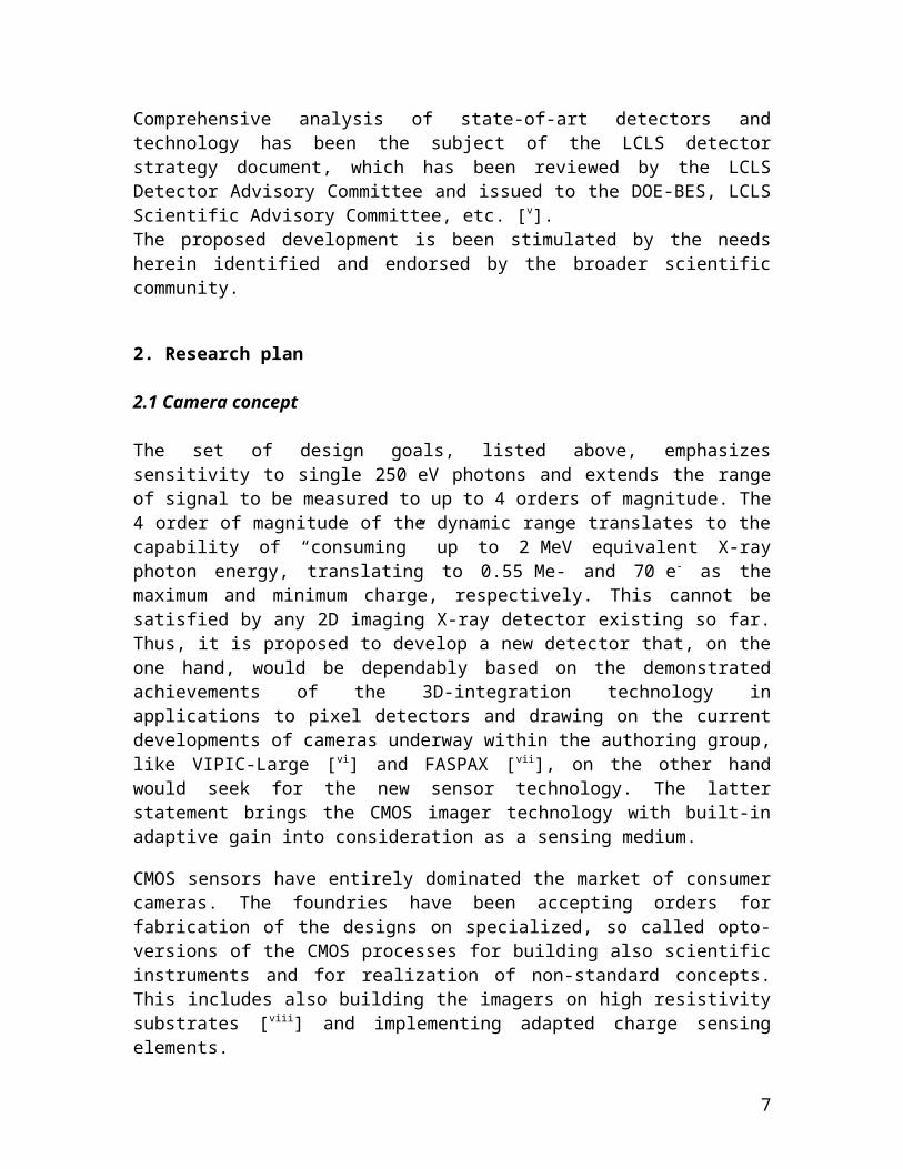
of the proposed camera, called 3D-integrated CMOS detector, as shown in Fig. 1, the CMOS imaging sensor is augmented by an additional layer of dedicated high-performance electronics, 3D integrated at the pixel level. The pixel in the CMOS sensor contains only minimal circuitry for the conversion of the charge packet into voltage or current right at the source of the signal; most functionality is located in the additional electronics layer. The charge conversion takes place with a very low parasitic capacitance, resulting in a high conversion factor, allowing very low noise performance. This feature is present for the smallest signals. The voltage or current signals, either for small or large signals, can then be processed in the electronics layer (readout ASICs) 3D integrated with the sensor.
Fig. 1. CMOS-based 3D integrated imager; multiple readout ASICs attached to a large size CMOS detectors using, for example, the low-temperature direct bonding or classical small pitch bump bonding technique and providing seamless coverage thanks to the pitch rerouting using metal layers of the CMOS sensor
The sensing part is a large-area, composed of multiple stitched reticles, CMOS imager. Therefore the CMOS imager is produced as a monolithic large area device, and in traditional CMOS integrated circuits this would lead to manufacturing yield reduction. In our concept, the much reduced circuit complexity on the CMOS sensor itself will be key for a reasonable manufacturing yield.
It is thinned to about 100 m, which is sufficient to stop X-rays in the energy range of (0.25-2 keV), to provide good detection efficiency, and simultaneously, thanks to the illumination from the backside, it yields sufficient shielding of its opposite side and components mounted there from being damaged by radiation.
The readout ASIC is segmented in a similar manner as the CMOS sensor, however pixel pitches are not the same on both components. By making the pixel pitch of the sensor larger than the pixel pitch of the readout ASIC and using routing metal layers that are usually available in the sufficient number in the CMOS process of the sensor, the pitches can be virtually tapered by adequate rerouting. By doing so, empty spaces can be gained between the readout ASICs, which on the one hand can be used for routing all the signals, power supplies and biases on the CMOS sensor slab,
6
making it a genuine support for the camera, and on the other hand, individual readout ASICs can be mounted on the sensor with greatly relaxed tolerances for their dimensions after dicing. Pitch adaptation also yields large area device with no seams in sensitivity visible.
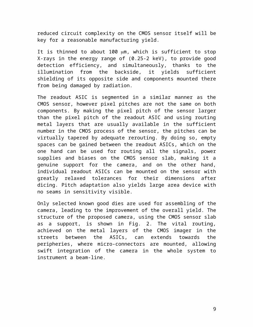
Only selected known good dies are used for assembling of the camera, leading to the improvement of the overall yield. The structure of the proposed camera, using the CMOS sensor slab as a support, is shown in Fig. 2. The vital routing, achieved on the metal layers of the CMOS imager in the streets between the ASICs, can extends towards the peripheries, where micro-connectors are mounted, allowing swift integration of the camera in the whole system to instrument a beam-line.
Fig. 2. Top view of the 3D-integrated CMOS detector with readout ASICs attached and vital routing achieved on the metal layers of the CMOS imager in the streets between the ASICs
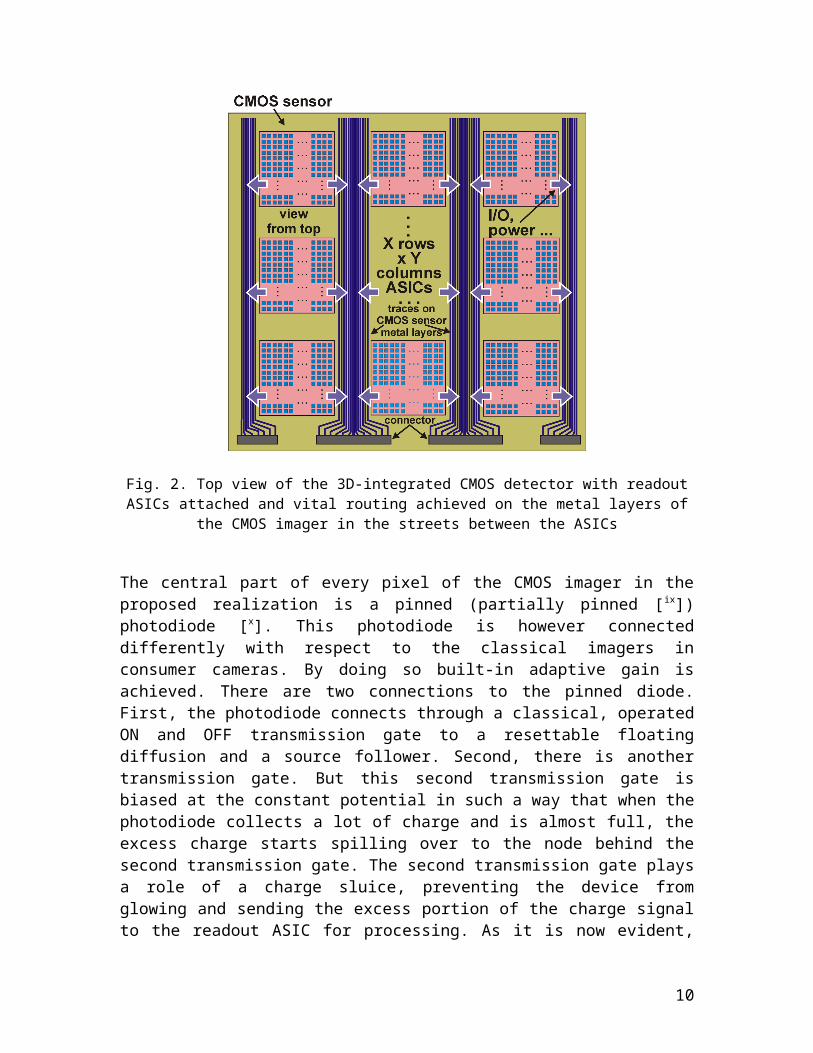
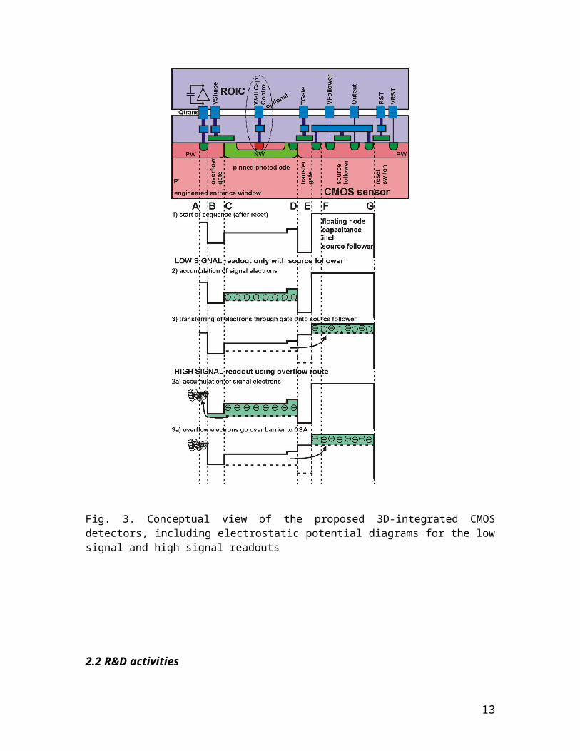
The central part of every pixel of the CMOS imager in the proposed realization is a pinned (partially pinned [ix]) photodiode [x]. This photodiode is however connected differently with respect to the classical imagers in consumer cameras. By doing so built-in adaptive gain is achieved. There are two connections to the pinned diode. First, the photodiode connects through a classical, operated ON and OFF transmission gate to a resettable floating diffusion and a source follower. Second, there is another transmission gate. But this second transmission gate is biased at the constant potential in such a way that when the photodiode collects a lot of charge and is almost full, the excess charge starts spilling over to the node behind the
7

second transmission gate. The second transmission gate plays a role of a charge sluice, preventing the device from glowing and sending the excess portion of the charge signal to the readout ASIC for processing. As it is now evident, the first transmission gate is a path for processing of small signals and the second transmission gate is a path for large signals.
A conceptual view of the proposed 3D-integrated CMOS detectors, including electrostatic potential diagrams for the low signal and high signal readouts, is shown in Fig. 3. The solution resembles another, proposed in the past, however that was realized in a fully customized way, which also postulated collection and transfer of electric charge within the same pixel, in the manner similar to the operation of Charge Coupled Devices, to a node performing the conversion to the voltage or current signal [xi].
The low signal path of the ASIC has a form of a classical processing with correlated double sampling for achieving the low noise performance. The required control signals, i.e. for reset of the floating diffusion node and for transfer of the charge from the photodiode to the floating diffusion are provided by the readout ASIC through the vertical connections. Also the output voltage of the source follower is sent to the readout ASIC through another vertical connection.
The large signal path of the ASIC is composed of a charge integrating amplifier located on the readout ASIC. The amplifier features virtual ground on its input and is capable of consuming charge flowing over the sluice in the CMOS imager.
The first diagram in Fig. 3 shows a distribution of the electrostatic potential after resetting of the floating diffusion and closing the transmission gate before any charge collection. The potential well of the pinned photodiode is empty there. The second diagram shows the case when a small portion of charge has been, first, collected by the pinned diode and then, after closing the transmission gate, this charge flows to the floating diffusion and can be sensed through the source follower. The small dimension of the floating diffusion provides the high conversion factor despite of the large side of the photodiode. The third diagram shows the case when during collection of charge, the pinned diode well potential fills above the limit at which the sluice activates and excess charge flows to the diffusion kept at the virtual ground potential by the charge integrating amplifier. Thus, one portion of the charge for large signals is measured by the charge integrating amplifier continuously during the charge collection process and the second portion of the charge is processed analogously to the small charge. The ratio between the portions processed through the two paths depends on the dimensions of the structure and the applied biases. Also the pinned diode can be implemented in such a way that the potential of its pinning layer can be additionally defined in order to control the full well capacity of the photodiode [xii] or it can be left floating in case the full well capacity does not need to be controlled.
8
The device is operated with back-side illumination. Its thickness, on the one hand, is chosen to get high detection efficiency for photons in the targeted energy range, and, on the other hand, shielding of the electronic components.
Fig. 3. Conceptual view of the proposed 3D-integrated CMOS detectors, including electrostatic potential diagrams for the low signal and high signal readouts
9
2.2 R&D activities
The R&D phase will have several components that would need to be tackled in parallel, but may require different levels of resources and time. These components can be listed as:
CMOS sensor Readout ASIC Assembly Testing
The decisive component for success of the project is the CMOS sensor. It is also an unknown as its structure is proposed for the first time despite of compiling several solutions separately demonstrated elsewhere. The proposed structure of the CMOS sensor, as it is presented in the previous paragraph, is only indicative, and, in order to achieve the postulated functionality, significant effort will have to be directed to:
Performing crude (using general technology data) TCAD CMOS sensor simulations [xiii,xiv] of the proposed structure to set the targets for further detailed device development; emphasis in simulation needs to be on making sure that good signal storage, complete transfer and complete clearing of charge can be achieved in every cycle. Also the maximum signal range achievable has to be studied in detail.
Engaging in discussions with foundries in order to establish a platform for reviewing process options offered by the foundries on their opto-process versions and implementing the required features; recently more foundries have offered access to processes with opto-features through MPW services and engineering runs; also some foundries offer flexibility of accepting adjustments to their standard process flows to accommodate, for example fabrication on high resistivity substrates and add other process features; a need for the latter may result from the first TCAD simulation steps; many of those are already involved in the development of naming available options, several companies can be listed, as for instance Tower Semiconductors - Jazz, that is already involved in pixels detectors for HEP such as the Internal Tracker System for the ALICE experiment at the LHC.
Developing our existing industry links to increase expertise levels, facilitate contact with the industry and gain collaborative support.
Designing and fabricating test structures to evaluate the implementation of a few design options in the chosen technology.
Designing and fabricating a first prototype of a simple structure that will allow testing of the proposed functionality; due to the nature of the CMOS process used for building this device, no need of attaching it to any readout ASIC will be required for testing (a simple readout scheme can share the same substrate – although this will not be substitutive for the target approach).
10
Start designing a real scale device to be implemented in full wafers for further development steps.
Leveraging capabilities available in other laboratories (e.g. LBNL, MIT-LL) or industry for thinning CMOS sensor wafers and engineering the entrance window to obtain sensitivity to 250 eV X-ray photons under back-side illumination.
The design of a readout ASIC will depend on the final form of the CMOS sensors. It will have to be tailored to multiple factors, like the required electrical levels of control signals, biases and power supplies that need to be provided on the CMOS sensor side by the readout ASIC, on the number of connections passing from the readout ASIC to the CMOS sensor and on the bonding technology. Thus, the design work can be started, first, focusing the attention on general aspects, and only then, to achieving matching with the sensor.
In response to the impinging X-rays the sensor will produce two types of signal, i.e. a signal in the voltage domain and another signal in the current domain. These two signals form a natural ranging of gains: for a small number of photons only the signal in the voltage domain will be significant, while the signal in the charge domain will be relevant for a large number of photons.
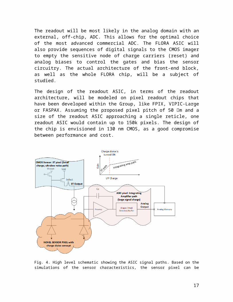
Therefore the front-end block of the pixel in the FLORA ASIC will have two paths (Fig. 4). The first path will buffer and filter the voltage response only. This will be the high sensitivity path, with the lowest input referred noise level, allowing detection of single photons of the lowest energy (250 eV). The second path will provide charge integration, buffering of the resulting voltage signal, and filtering. Actual implementation of this path will require more detailed studies for the choice of the integration technology.
Basically two approaches for an integrator can be considered. The first one is a system with an integration capacitance connected in a feedback path of a high negative gain amplifier. The second one can be seen as a passive integrator, with an integration capacitor buffered by a current conveyor, and the input current transferred from the input node to the node with the connected capacitance. The second solution may use a bipolar or MOS transistor in the common base or common source configuration, respectively, similarly to the FASPAX recently developed by the Fermilab ASIC Group for the APS.
As the voltage path will work up to about ten 250 eV X-ray photons and the integration path will have to cover the remaining more than three orders of magnitude, further splitting of the sensitivity of the integration path into more ranges, e.g. two with different gains, may be necessary to cover the desired dynamic range. This splitting of the sensitivity can be obtained by switching (adaptively to the acquired signal) capacitances in the feedback path or by two or more current conveyors, with different gains, working simultaneously. The front-end block will
11
have to select on which range should be read out. The result of every integration will be sampled and stored for the readout.
The readout will be most likely in the analog domain with an external, off-chip, ADC. This allows for the optimal choice of the most advanced commercial ADC. The FLORA ASIC will also provide sequences of digital signals to the CMOS imager to empty the sensitive node of charge carriers (reset) and analog biases to control the gates and bias the sensor circuitry. The actual architecture of the front-end block, as well as the whole FLORA chip, will be a subject of studied.
The design of the readout ASIC, in terms of the readout architecture, will be modeled on pixel readout chips that have been developed within the Group, like FPIX, VIPIC-Large or FASPAX. Assuming the proposed pixel pitch of 50 m and a size of the readout ASIC approaching a single reticle, one readout ASIC would contain up to 150k pixels. The design of the chip is envisioned in 130 nm CMOS, as a good compromise between performance and cost.
Fig. 4. High level schematic showing the ASIC signal paths. Based on the simulations of the sensor characteristics, the sensor pixel can be comprised of the charge sluice and a standard 3 transistor (3T) low signal path for small charges, this would be an ultra-low noise path to meet the design specification of < 10e-rms at the low end of the dynamic range. The ASIC pixel provides the alternate charge integrating amplifier path would be used when the charge sluice is turned ON. Additionally the ASIC would also provide all the biasing and control signals to the 3T CMOS sensor. The 3T output and/or the Analog output will be stored in memory. To enable fast frame readouts with effective speeds >10 kHz, multiple parallel outputs can be provided to enable
12
simultaneous readout of multiple pixels as shown in figure. This is also subject of study for other developments (e.g. FASPAX).
The next item on the list is the bonding technology. Since up to 10 connections per pixel between the readout ASIC and the CMOS sensor may be required, bump bonding may not be up to the task. However, very dynamic development of the low-temperature direct bonding technology that was also successfully demonstrated on the chip-to-wafer basis, will probably be the choice for the proposed project. In this R&D phase features required for the 3D bonding will be included in the design of the CMOS sensor and ASIC. Some functionalities of the prototype ASIC will also be contained in the peripheral part of the sensor where the chip will be bonded for the purpose of testing a full system-like prototype.
The last item on the list is testing of the prototype devices. Extensive tests of the prototype are planned both with lab x-ray sources and at SLAC users facilities. Several aspects of the design will have to be investigated: charge collection efficiency, gain, linearity, readout speed, uniformity, quantum efficiency, etc. Both SLAC and Fermilab have radioactive sources available for lab tests, and beamtime at SSRL and LCLS is available for LCLS detector characterization and calibration.
An overview of the schedule is shown in Figure 5.
3. Future development
After successful completion of the R&D phase we plan to move forward with the development of a full size camera. This will require full size CMOS sensors and ASIC, and the implementation of the 3D bonding, not covered by the present effort. Suitable schemes with associated electrical and mechanical design for tiling the modules over a large area (~ 10 cm x 10 cm) have to be developed. Integration in the LCLS DAQ system and development of data handling schemes will exploit the advantages of such a type of detector over CCDs (e.g. Region of Interest).Once the full camera performance will be demonstrated, transfer to mass production mode will be facilitated by the intrinsic nature of our detector, i.e. commercially available technology used for the CMOS sensor. Although the detector will be developed to meet the requirements of the new instruments currently being designed for NEH 1.1 and NEH 2.2 at LCLS, other light sources will benefit of the achieved advancement in performance. Electrical and material sensitivity fulfill the need not only for photon but also electron detection (e.g. TEM). The basic concept of the detector can be implemented also for hard x-rays extending the range of application for such type of detector.
13
Fig. 5. Schedule overview.
4. Management plan
Gabriella Carini and Grzegorz Deptuch will be responsible to DOE for the management and execution of the scope of this work. SLAC and Fermilab will form an Institutional Agreement defining the collaboration. Both labs will report progress to DOE on a regular basis and track adherence to the proposed schedule.
The scope of work will be contained in a resource-loaded schedule managed by SLAC and Fermilab. For scope and requirements modifications, a Change Control Process will be jointly implemented by SLAC and Fermilab. The schedule will make clear the institutional responsibilities and interfaces for the work described above. SLAC and Fermilab will jointly review progress and update the schedule on a monthly basis. At each major design stage, SLAC and Fermilab will jointly review the proposed designs, for technical completeness, risks and risk mitigations. To guarantee a good level of communication and coordination bi-weekly teleconferences for technical discussion and development are planned for the whole duration of the project. In person meetings are expected twice per year.
SLAC and Fermilab will share design documents, such as layout, schematics and mechanical designs, on a joint website. Co-developed firmware and software will be version-controlled with a shared repository.
14

The FLORA project will be a standing agenda item reviewed by the LCLS Detector Advisory Committee (LDAC). The LDAC will advise the management team on issues relating to the development of the FLORA detector.
5. References
15
i https://portal.slac.stanford.edu/sites/lcls_public/Pages/Default.aspxii White W, Robert A and Dunne M, Journal of Synchrotron Radiation (2015) 22, 472 and references thereiniii https://portal.slac.stanford.edu/sites/lcls_public/Lists/machine_faq/FAQ.aspx iv https://portal.slac.stanford.edu/sites/lcls_public/lcls_ii/Pages/default.aspxv Carini G., “LCLS Detector Development Strategy”, Sep 2015.vi Deptuch G W, et al., DOI 10.1109/TED.2015.2448671vii Bradford R, ANL Users’ meeting communicationsviii https://indico.cern.ch/event/309449/overviewix Lee T H, et al., US Patent 5,903,021x Fossum E R, Hondogwa D B, IEEE J. of the Electron Devices Society, Vol. 2, No. 3, 2014, 33xi Carini G A, et al., Nucl. Instr. And Method, A 649, 2011, 75-77xii Y. Hagiwara, Japanese Patent JP,52-058414,Axiii Yiqiang L, et al., Journal of Semiconductors, Vol. 33, No. 12, 2012, 124004-1-124004-6xiv Yiqiang L, et al., Journal of Semiconductors, Vol. 32, No. 12, 2011, 124008-1-124008-4
Appendix 1: Biographical Sketches
Gabriella Carini 2575 Sand Hill Rd – MS 10Staff Scientist, Menlo Park, 94025 CA
LCLS, SLAC National Accelerator Laboratory [email protected]
Professional PreparationUniversity of Palermo, Italy M. Sc. 2001 Electrical EngineeringUniversity of Palermo, Italy Ph. D. 2006 Electrical EngineeringBrookhaven National Laboratory, NY Post-Doc 2008 Applied Physics
AppointmentsNational Synchrotron Light Source, BNL 2008-2010 Assistant Physicist
National Synchrotron Light Source, BNL 2010-2011 Associate PhysicistSLAC National Accelerator Laboratory 2011- to date Staff ScientistLCLS, Detector Department, SLAC 2015- to date Department Head
Publications closely related to the project
1. G.W. Deptuch, G. Carini, P. Enquist, P. Gryboś, S. Holm, R. Lipton, P. Maj, R. Patti, D.P. Siddons, R. Szczygieł, R. Yarema, “Fully 3D-integrated Pixel Detectors for X-Rays“, IEEE Transaction on Electron Devices, vol. 63, no. 1, (2016), pp. 205-214
2. G. Blaj, P. Caragiulo, G. A. Carini, S. Carron, a. Dragone, D. Freytag, G. Haller, P. Hart, J. Hasi, R. Herbst, S. Herrmann, C. Kenney, B. Markovic, K. Nishimura, S. Oiser, J. Pines, B. Reese, J. Segal, A. Tomada, M. Weaver, “X-ray detectors at the Linac Coherent Light Source”, J. Synchrotron Rad. (2015), 22, 577-583.
3. G. A. Carini, P. Rehak, W. Chen, D. P. Siddons, “Charge-Pump Detector for X-ray Correlation Spectroscopy“, Nucl. Instr. Meth. A, 649 (2011) 75–77.
4. G. A. Carini, W. Chen, A. Dragone, J. Fried, J. Jakoncic, A. Kuczweski, Z. Li, J. Mead, R. Mitcha, J.-F. Pratte, P. Rehak and D. P. Siddons, “Tests of small X-ray Active Matrix Pixel Sensor prototypes at the National Synchrotron Light Source”, 2009 JINST 4 P03014.
5. G. A. Carini, W. Chen, G. De Geronimo, J. A. Gaskin, J. W. Keister, Z. Li, B. D. Ramsey, P. Rehak, D. P. Siddons, “Performance of a Thin-Window Silicon Drift Detector X-ray Fluorescence Spectrometer”, IEEE Trans. Nucl. Sci., vol. 56 (5), 2843 (2009).
Synergistic activities
2016 Co-organizer, International Forum on Detectors for Photon Science, Mount Fuji, Japan.
2014, 2015, Topic convener, ‘Synchrotron radiation and FEL instrumentation’,2016 IEEE Nuclear Science Symposium.2014, 2015, Co-chair, ‘Synchrotron radiation and FEL instrumentation’ session, IEEE Nuclear
Science Symposium.2014 Topic convener, “Photodetectors’, TIPP 2014, Amsterdam (NL).2013, 2014 Chair, ‘Detector workshop’, SSRL-LCLS users’ meeting, SLAC2013 Co-chair, Detectors workshop’, 17th Pan-American Synchrotron Radiation
Instrumentation Conference.2013 Co-editor, Report of the DOE-BES sponsored workshop on ‘Photon and Neutron
Detectors’.2012 Co-organizer and co-chair, DOE-BES sponsored workshop on ‘Photon and Neutron
Detectors’.2008, 2012, Co-chair, ‘New Concepts in Solid-State Detectors’ session, IEEE 2013 Nuclear Science Symposium2005 - to dateReviewer for premier journals and DOE-NP SBIR, DOE-BES SBIR, DOE-BES EC, user
facilities and other international proposals.2003 - to date IEEE member
Collaborators and other affiliationsCollaborators and co-editors (collaborators currently at SLAC are not listed).

Chen, Wei (BNL); Chuang, Hui-Fang (NSRRC); De Geronimo, Gianluigi (BNL); Denes, Peter (LBNL); Deptuch, Grzegorz (Fermilab); Fahim, Farah (Fermilab); Fajardo, Pablo (ESRF), Erlbacher, Tobias (IISB-Fraunhofer); Gaskin, Jessica (NASA-MSFC); Graafsma, Heinz (DESY), Gruner, Sol (Cornell); Hatsui, Takaki (Riken/SPring8), Jakoncic, Jean (BNL); Kierster, Jeff (BNL); Kirkham, Robin (CSIRO); Menk, Ralf (Elettra); O’Connor, Paul (BNL); Pratte, Jean-Francois (U. Sherbrooke); Ramsey, Bryan (NASA-MSFC; Rumaiz, Abdul (BNL); Ryan, Chris (CSIRO); Siddons, Peter (BNL); Smith, Graham (BNL); Wiest, Florian (Ketek), C. B. Wunderer (DESY)
Graduate/Post-doc advisorsGraduate advisors: Prof. Claudio Arnone (University of Palermo), Dr. Ralph James (Brookhaven National Laboratory)Post-doctoral advisor: Dr. D. Peter Siddons (Brookhaven National Laboratory)
Graduate students/post-doc advised (2): Dr. Jinghui Wang (Stanford University)
Grzegorz W. DeptuchEngineer IV PO BOX 500 MS 222PPD/EED ASIC Development Group Batavia IL 60510
Fermi National Accelerator Laboratory [email protected]
a. Professional Preparation
Institution Location Major Degree & YearAGH - University of Science Kraków, Poland Electrical Engineering M.Sc. 1991–96and Technology ElectronicsUniversité Strasbourg I and Strasbourg, France Physics/Electronics
Ph.D. 1999–2002 AGH - University of Science Kraków, Polandand TechnologyLaboratoire d'Electronique Strasbourg, France Post-Doc 2002-2004et de Physique des SystèmesInstrumentaux (LEPSI/ULP/IN2P3)AGH - University of Science Kraków, Poland Electronics D.Sc. 2014and Technology b. Appointments:
2007 – current Fermi National Accelerator Laboratory (Fermilab), Batavia, IL, ASIC Engineer
2011 – current Engineer IV (Senior Principal), Head of the ASIC Development Group
2010 – 2011 Engineer IV (Senior Principal), Deputy Head of the ASIC Dev. Group2008 –2010 Engineer IV, Assistant Group Leader2008 –2008 Engineer III, Assistant Group Leader2007 –2008 Engineer III
2015 – current AGH - University of Science and Technology, Poland; Adjunct Professor 2005 – 2007 Brookhaven National Laboratory (BNL), Instrumentation Division – Assistant Physicist
2002 – 2005 AGH - University of Science and Technology, Poland; Assistant Professor1996 –2002 AGH - University of Science and Technology, Poland; Research Assistant
c. Publications closely related to the project:6. G.W.Deptuch, G.Carini, P.Enquist, P.Gryboś, S.Holm, R.Lipton, P.Maj, R.Patti, D.P.Siddons,
R.Szczygieł, R.Yarema, “Fully 3D-integrated Pixel Detectors for X-Rays“, IEEE Transaction on Electron Devices, vol. 63, no. 1, (2016), pp. 205-214
7. G.Deptuch, M.Demarteau, J.Hoff, R.Lipton, A.Shenai, M.Trimpl, R.Yarema, T.Zimmerman, “Vertically Integrated Circuits at Fermilab“, IEEE Trans Nucl Sci, vol. 57, no. 4, (2010), 2178-2186
8. G.Deptuch, “Monolithic Pixel Detectors in a Deep Submicron SoI Process“,Nucl. Instr. and Meth., A623, (2010), pp.183-185.
9. G.Deptuch, A.Besson, P.Rehak, M.Szelezniak, J.Wall, M.Winter, Y.Zhu, “Direct Electron Imaging in Electron Microscopy with Monolithic Active Pixel Sensors“, Ultramicroscopy, 107, (2007), pp.674-684
10. G.Deptuch, W.Dulinski, M.Caccia, M.Winter, “High Resolution, Back-Side Illuminated Monolithic Active Pixel Sensor for Low Energy Electron Imaging”, IEEE Transaction on Nuclear Science, vol. 52, no. 5, (2005), pp. 1745-1754
d. Synergistic Activities
1. Author and co-author of more than 100 journal and conference papers, including about 80 papers in journals from Thomson ISI Master Journal List, more than 850 citations excluding self-citation, Hirsch index equal to 17.
2. Presenter of numerous talks to international conferences, workshops, discussion forums and several invited international contributions.
3. Peer reviewer (more than 40 reviews accomplished) of papers for journals like: Nuclear Instruments and Methods A, IEEE Transaction on Nuclear Science, IEEE Transaction on Circuits and Systems I, IEEE Sensors Journal, SISSA and IOP Journal on Instrumentation, MDPI Sensors.
4. Reviewer for: Department of Energy (DoE) SBIR grant proposals (about 10 reviews accomplished), the Polish Science Foundation and development projects of new detectors, PhD defence board at the Universite de Strasbourg I, ULP, Strasbourg, France and AGH-UST, Krakow, Poland.
5. Member: IEEE since 1998 (senior member since 2007), Electron Devices and Circuits and Systems Societies.

e. Collaborators and other affiliations:
F.Fahim (Fermilab); J.Hoff (Fermilab); A.Shenai (Fermilab); T.Zimmerman (Fermilab); R.Yarema (Fermilab); S.Holm (Fermilab); D.Christian (Fermilab); R.Lipton (Fermilab); M.Demarteau (Argonne); M.Trimpl (KLA-Tencor); Q. Zhang (Argonne); E. Dufresne (Argonne); S.Narayanan (Argonne); A.Sandy (Argonne); R. Bradford (Argonne), J. Weizeorick (Argonne); T. Madden (Argonne); P.Siddons (BNL); A. Rumaiz (BNL); J.Mead (BNL); G. Carini (SLAC); P. Grybos (AGH-UST); P. Maj (AGH-UST); R. Szczygiel (AGH-UST); P. Gui (SMU). G. Wu (SMU);
f. Graduate Advisors and Post-Doctoral Sponsors (3 Total)
PhD Thesis Advisor(s): Stanislaw Kuta from AGH-UST, Krakow, Poland and Ulrich Goerlach from ULP, Strasbourg I, France. Post-doc Advisor(s): Wojciech Dulinski from LEPSI/ULP/IN2P3 Strasbourg France, Marc Winter from IReS/IN2P3, Massimo Caccia from University of Como, Como, Italy
g. Thesis Advisor and Post-Graduate Scholar SponsorCurrently Aleksandra Krzyzanowska AGH-UST, Krakow Poland
Farah Fahim PO Box 500 – MS 222Engineer III, Batavia, 65010 ILPPD, Fermi National Accelerator Laboratory [email protected]
Professional PreparationUniversity of Limerick, Ireland B.Tech 2003 IT & TUniversity of Limerick, Ireland M.Tech 2009 Analog IC DesignNorthwestern University PhD current Electrical Engineering
AppointmentsRutherford Appleton Laboratory, UK 2005-2006 Graduate EngineerRutherford Appleton Laboratory, UK 2006-2009 EngineerFermi National Accelerator Laboratory 2009-2014 Engineer IIFermi National Accelerator Laboratory 2014- current Engineer III
Publications closely related to the project
Farah Fahim ; Grzegorz W. Deptuch ; James R. Hoff and Hooman Mohseni" Design methodology: edgeless 3D ASICs with complex in-pixel processing for pixel detectors ", Proc. SPIE 9555, Optical Sensing, Imaging, and Photon Counting: Nanostructured Devices and Applications, 95550M (August 28, 2015); doi:10.1117/12.2188153; http://dx.doi.org/10.1117/12.2188153
Farah Fahim ; Grzegorz W. Deptuch ; James R. Hoff and Hooman Mohseni" Modeling and analysis of hybrid pixel detector deficiencies for scientific applications ", Proc. SPIE 9555, Optical Sensing, Imaging, and Photon Counting: Nanostructured Devices and Applications, 955517 (August 28, 2015); doi:10.1117/12.2188128; http://dx.doi.org/10.1117/12.2188128
Synergistic activitiesDevelopment of FASPAX Interposer with CVI, Inc.Design and development of VIPIC Digital ASIC
Collaborators FASPAX: Argonne National Laboratory, CVI Inc VIPIC-L: Argonne National Laboratory, Brookhaven National Laboratory, AGH-UST Krakow
Graduate advisorsGraduate advisors: Prof. Hooman Mohseni (Northwestren University), Dr. Grzegorz Deptuch (Fermi National Accelerator Laboratory)
Appendix 2: Current and Pending Support

Gabriella Carini
01/16 - 09/17 Co-PI, DOE-BES “Very Fast Charge Coupled Device (CCD) for Soft X-ray Experiments at LCLS-II”, Co-PI Peter Denes, LBNL, Berkeley, CA.
07/15 – 06/17 Co-Investigator, NIH-R21 PR637354 ‘Charge Cloud Tracker : A High-Resolution, High-DQE, Photon-Counting Energy Discriminating X-ray Detector’, PI Norbert J Pelc, Department of Bioengineering, Stanford University, Menlo Park, CA.
04/15 - 03/17 Co-PI, Coulter Translational Research Project Award SPO120187 ‘Charge Could Tracker: A High-Res Photon-Counting X-Ray Detector’, Co-PI Norbert J Pelc, Department of Bioengineering, Stanford University, Menlo Park, CA.
04/14 - 09/16 PI, SLAC LDRD ‘cPix2: multi-gate area detector for MHz repetition rate pump-probe experiments’
Grzegorz Deptuch (PI/co-PI):
a. “1 Megapixel Detector for X-ray correlation Spectroscopy” (FWP FNAL 14-16),
b. 2013 U Chicago Strategic Collaborative Initiative Award "An Advanced, five orders of magnitude dynamic range, wafer scale pixel system for X-ray science”, (R6C613)
c. “Development of Application Specific Integrated Circuits (ASICs) for Synchrotron X-ray Detectors” (R3A124)
Appendix 3: Facilities, Other Resources, and Equipment
SLACAn extensive collection of equipment, computing resources, on-site machining and fabrication shops are available for use on this project as well as access to the Stanford Nanofabrication Facility, Stanford Nano-Center and Stanford Nanocharacterization Laboratory on the Stanford campus.In addition to the resources in SLAC campus, the LCLS detector group is establishing two working areas in the metrology cleanroom and in a dedicated laboratory with a variety of tools for inspection, power supplies, oscilloscope, vacuum pump, stages and chillers. Radioactive sources
and fast optical lasers are available for test and characterization as well as beamtime at SLAC users facilities, i.e. SSRL and LCLS.
Stanford NanofacilitiesThe Stanford Nanofacilities are shared resources in Stanford Campus serving academic, industrial, and governmental researchers across the U.S. and around the globe. A series of cleanrooms with a full suite of tools supporting device fabrication, advanced characterization and analysis is available 24 hours a day, 7 days a week.
SSRL experimental station 13-1The experimental station 13-1 at SSRL provides a chamber designed to accommodate a wide range of setups. Table 4 summarizes its primary characteristics. This is the primary location for testing our prototypes during SSRL AP mode. Other endstations may be used for in air tests at higher energies.
Table 4: Characteristics of the SSRL - experimental station 13-1
Source characteristics Elliptically polarized undulator
Energy range 250 eV- 1250 keV (monochromatic)
Monochromator 3 water-cooled interchangeable
Flux 10^11 photons/sec in 1 mm x 1 mm
Resolving power (E/ E)Δ 5000
LCLS SXR Instrument.The SXR instrument is the soft X-ray monochromatic beamline at the LCLS. SXR is designed to accommodate a wide range of experimental end stations and is the primary location where the prototype detectors will be tested under FEL conditions. Table 5 summarizes the primary SXR characteristics.
Table 5: Characteristics of the LCLS SXR instrument.

Source characteristics Bend magnet
Energy range 250 eV- 2 keV (monochromatic)
Monochromator Varied Line Spacing Plane Grating
Flux (150 pC, 120 Hz, 50 fs) ~1 x 10¹³ photons/s/3x10-4BW
(~1x10¹¹ photons/pulse/3x10-4BW)
Resolving power (E/ E)Δ 3000
Fermilab
Fermilab ASIC Development Group currently creates a core of 6 ASIC designers - including 3 PhDs. Two designers are at the senior-leader position, one is currently pursuing the PhD degree. The Group is currently in the process of hiring two more designers, i.e. one at the senior and one at the junior level in order to meet the needs of the projects. This level of stuffing makes the Fermilab ASIC Development Group the biggest ASIC-oriented team among the National Laboratories System and the US Universities. The ASIC Development Group ASIC also provides testing, where the resources are as follows: one engineering physicist with PhD, one test engineer, one engineering associate, one technician and one PCB drafter. The ASIC Development Group provides internally resources for maintenance of CAD/EDA tools, licenses, scripts, etc. and occasionally receives support from other members of the Fermilab Particle Physics Division, Computing Division and other departments at Fermilab. The role of the ASIC Development Group consists in providing integrated circuits for detectors to run experiments and to convey R&D on detectors for future applications. Design projects are acquired by the Group through several avenues, where the most popular is bringing projects directly to the group by/from physicists involved in experiments. Also, new projects are started internally or in response to external requests based upon the reputation of the group and portfolio of explored technologies. The Group also responds to project calls if such calls are aligned with the Group activities and interests and if involvement in such new projects is beneficial for the Group, e.g. if it allows gaining new experiences and growing the project portfolio. The area of operation of the ASIC Group is primarily instrumentation for HEP, however, secondarily, the Group efforts are also applied, where synergies are possible, and where allocation of thee Group resources is appropriate. The ASIC Group developed extensive collaboration network and works through these collaborations, both, domestically (ANL, BNL Southern Methodist University, UPenn) and internationally (CERN, AGH-UST Krakow Poland, U. of Bergamo Italy). The presence of the Fermilab ASIC Group maintains core competences for niche designs in extreme environments (cold, radiation) and is a platform for projects that are challenging and have potential of changing the field. The presence of the Group guarantees also maintaining legacy projects and provides long term expertise on thee chips designed in the past. The Group also provides a base for collaboration with Universities.

The portfolio of projects that have been recently active for 1 year includes the following chips: QIE10 in AMS 0.35 BiCMOS – PMT readout, 4m of cable Zin=50 production for CMS, QIE11 in AMS 0.35 BiCMOS – SiPM readout, adjustable gain 10× production for CMS, QIE12 in AMS 0.35 BiCMOS – like QIE11 but 1.5 fC/LSB tested OK for ATLAS waiting for the decision, VIPRAM3D, VIPRAML1CMS in GF 130 CMOS and 3D – 3D integrated pattern recognition processors for HL-LHC hardware tracker, FCP130 / IFCP65 in GF 130 CMOS and in TSMC 65 CMOS – fast, synchronous front-end, integrated with 2-3 bit resolution ADC as pixel front-end prototypes for HL-LHC within the RD53 activities, COLDATA in TSMC 65 CMOS - 8×200Mbs translation to 2×1.25Gbps over 25 m cables from lAr cryostat to the warm side in DUNE and control of FE and ADC chips, VIPIC-Large in GF 130 CMOS and 3D – 3D integrated pixel detector for XPCS experiments in photon science >120M transistors in a single chip, FASPAX in GF 130 BiCMOS – semi-3D integrated, seamless pixel detector for the APS upgrade allowing DR=105. The ASIC Group also maintains ASIC test lab spaces, where major components are: an ESD controlled “clean room” with semi-automatic probe stations /one capable of 8” wafers/ and measurement instruments (LCR meter, DC-3GHz spectrum analyzer, static parameter analyzer, Logic analyzers, network analyzer, V/I sources, pA meters, digital oscilloscopes, etc.), four PXI/PXIe FlexRIO National Instruments digital and analog (ADC, DIO LVDS, DIO CMOS, DAC, SMU, DMM, power, etc.) systems based on LabView/Labview FPGA and RT – to fulfill hardware needs for testing of chips, typical laboratory radioactive sources, a robotic chip testing station, two manual bonding stations and a fully equipped PCB components mounting lab. The level of expertise and the facility, both, allow realization of the proposed R&D project on the 3D-integrated CMOS pixel detector for detection of low energy X-rays.
Appendix 4: Data Management Plan
1. Expected dataDuring this project data concerning detector R&D, i.e., technology and methodologies, will be produced. LCLS and Fermilab will follow the practices described below for management of data concerning the development of this detector. The primary intellectual output of this effort will be shared with the scientific community at conferences and through publications in journals and proceedings. Data taken during tests at LCLS will follow the LCLS Data Retention Policy available at: https://confluence.slac.stanford.edu/display/PCDS/Data+Retention+Policy.
2. Data and metadata formatDatasets will be stored as electronic files and backed up at Fermilab and SLAC. LCLS data typically comes in the form of x-ray detector data along with metadata describing the experimental conditions at the instrument as well as for the entire LCLS machine. The data is initially store in a binary format called xtc which includes all user-selected data and metadata. The data is saved to disk and available for use by the user groups via authentication. The users granted access to the data are selected by the PI of the particular experiment. More information

is available here https://confluence.slac.stanford.edu/display/PCDS/Computing. Data is stored to disk for some time and then moved to tapes for archiving in a manner consistent with the LCLS Data Retention Policy.Experimenters are provided access to an online logbook to store comments and lab notes related to their experimental data. This elog is accessible via authentication of users approved by the PI of the given experiment here: https://pswww.slac.stanford.edu/.
3. Policies and practices for access and sharingData posted to journals and conference will be fully available to the public. We will also share high-level schematics. However it is common practice in design and fabrication of CMOS sensors and ASICs that foundries and providers of software development tools consider proprietary specific data files that can only be accessed after signing nondisclosure agreement (NDA).
4. Policies and provisions for re-use, re-distributionIn case other groups would like to use our data, we will make them available, when possible without NDA infringement, and consider case-by-case if our contribution may warrant co-authorship or simple reference to our work.
5. Plans for archiving and preservation of accessData will be backed in the Fermilab and SLAC servers and managed according to the labs standards.


![LLRF System for LCLS-II at SLAC - KEK · 2013. 6. 4. · April 8, 2011, Chapter 6, Accelerator [2] Z. Geng, LCLS-II Injector LLRF System-MicroTCA Based Design , SLAC, June, 4, 2012,](https://static.fdocuments.in/doc/165x107/60e42a9b7f183a545b3171d0/llrf-system-for-lcls-ii-at-slac-kek-2013-6-4-april-8-2011-chapter-6-accelerator.jpg)


