


CDB5461AU CDB5461AU Evaluation Board & Softwarecontroller and a USB interface. Additionally,...
36
Copyright © Cirrus Logic, Inc. 2006 (All Rights Reserved) http://www.cirrus.com CS5461A C8051F320 +2.5V reference USB Reset Circuirty SERIAL EERPOM RESET BUTTON CS SDI SDO SCLK INT RESET E1 E2 E3 MODE VIN+ VIN- IIN+ IIN- REF +5V GND VD+_EXT Vu+_EXT IN OUT VREF 4.096MHz Crystal \ CDB5461AU CDB5461AU Evaluation Board & Software Features Voltage and Current Interface USB communication with PC On-board C8051F320 microcontroller On-board Voltage Reference Lab Windows ® / CVI™ Evaluation Software – Register Setup & Chip Control – FFT Analysis – Time Domain Analysis – Noise Histogram Analysis "Auto-boot" Demo with serial EEPROM – Collected by On-board Microcontroller – Available on External Header General Description The CDB5461AU is an inexpensive tool designed to evaluate the functionality and performance of the CS5461A. The evaluation board includes an LT1019 voltage reference, a C8051F320 microcontroller with a USB interface, and firmware. The microcontroller controls the serial communication between the evalu- ation board and the PC via the firmware, enabling quick and easy access to all of the CS5461A's regis- ters and functions. The CDB5461A includes software for Data Capture, Time Domain Analysis, Histogram Analysis, and Fre- quency Domain Analysis. ORDERING INFORMATION CDB5461AU Evaluation Board DEC ‘06 DS661DB1
Transcript of CDB5461AU CDB5461AU Evaluation Board & Softwarecontroller and a USB interface. Additionally,...

Copyright © Cirrus L(All Rights Rehttp://www.cirrus.com
CS5461A
+2.5V reference
E
CS
SDI
SDOSCLK
INT
RESET
E1
E2
E3
MODE
VIN+
VIN-
IIN+
IIN-
REF
+5V GND VD+_EXT
IN OUTVREF
4.096MHz Crystal
\
CDB5461AU
CDB5461AU Evaluation Board & Software
FeaturesVoltage and Current Interface
USB communication with PC
On-board C8051F320 microcontroller
On-board Voltage Reference
Lab Windows® / CVI™ Evaluation Software– Register Setup & Chip Control– FFT Analysis– Time Domain Analysis– Noise Histogram Analysis
"Auto-boot" Demo with serial EEPROM– Collected by On-board Microcontroller– Available on External Header
General DescriptionThe CDB5461AU is an inexpensive tool designed toevaluate the functionality and performance of theCS5461A. The evaluation board includes an LT1019voltage reference, a C8051F320 microcontroller witha USB interface, and firmware. The microcontrollercontrols the serial communication between the evalu-ation board and the PC via the firmware, enablingquick and easy access to all of the CS5461A's regis-ters and functions.
The CDB5461A includes software for Data Capture,Time Domain Analysis, Histogram Analysis, and Fre-quency Domain Analysis.
ORDERING INFORMATIONCDB5461AU Evaluation Board
ogic, Inc. 2006served)
C8051F320
USB
Reset Circuirty
SERIALERPOM
RESET BUTTON
Vu+_EXT
DEC ‘06DS661DB1
CDB5461AU
TABLE OF CONTENTS– TABLE OF CONTENTS ............................................................................................................. 2– LIST OF FIGURES ..................................................................................................................... 3– LIST OF TABLES ...................................................................................................................... 31. HARDWARE ............................................................................................................................. 4
1.1 Introduction ........................................................................................................................ 41.2 Evaluation Board Overview ................................................................................................ 4
1.2.1 Analog Section ...................................................................................................... 51.2.2 Digital Section ....................................................................................................... 61.2.3 Power Supply Section ........................................................................................... 7
1.3 Auto-boot Mode ................................................................................................................. 82. SOFTWARE .............................................................................................................................. 9
2.1 Installation Procedure ........................................................................................................ 92.2 Using the Software ............................................................................................................. 92.3 Start-Up Window ................................................................................................................ 9
2.3.1 Setup ................................................................................................................... 102.3.2 Quit ...................................................................................................................... 112.3.3 Menu ................................................................................................................... 12
2.4 Setup Window .................................................................................................................. 122.4.1 Refresh Screen Button ........................................................................................ 132.4.2 Reset DUT Button ............................................................................................... 132.4.3 CS5461A Crystal Frequency ............................................................................... 132.4.4 Configuration Register Panel .............................................................................. 142.4.5 Mask Register/Status Register Panel ................................................................. 142.4.6 Cycle Count / PulseRateE / PulseWidth / VSAGlevel / VSAGduration Registers 142.4.7 Control Register .................................................................................................. 14
2.5 Calibration Window .......................................................................................................... 152.5.1 Offset & Gain Registers ...................................................................................... 152.5.2 Performing Calibrations ....................................................................................... 15
2.6 Conversion Window ......................................................................................................... 172.6.1 Single Conversion Button .................................................................................... 172.6.2 Continuous Conversion Button ........................................................................... 172.6.3 Standby & Sleep Mode Buttons .......................................................................... 172.6.4 Power Up Button ................................................................................................. 182.6.5 Temperature Settings Window ............................................................................ 182.6.6 Write Data to File Window ................................................................................... 18
2.7 Pulse Rate Window .......................................................................................................... 182.7.1 Integration Seconds Field ................................................................................... 182.7.2 Periods to Average Field ..................................................................................... 182.7.3 Start Button ......................................................................................................... 19
2.8 Data Collection Window ................................................................................................... 192.8.1 Time Domain / FFT / Histogram Pull-down ......................................................... 192.8.2 Config Button ...................................................................................................... 192.8.3 Collect Button ...................................................................................................... 202.8.4 Output Button ...................................................................................................... 202.8.5 Zoom Button ........................................................................................................ 202.8.6 Channel Select Button ........................................................................................ 202.8.7 Config Window .................................................................................................... 202.8.8 Collecting Data Sets ............................................................................................ 212.8.9 Retrieving Saved Data from a File ...................................................................... 212.8.10 Analyzing Data .................................................................................................. 212.8.11 Histogram Information ....................................................................................... 222.8.12 Frequency Domain Information ......................................................................... 24
2 DS661DB1

CDB5461AU
2.8.13 Time Domain Information .................................................................................. 252.9 EEPROM Window ........................................................................................................... 26
2.9.1 Read EEPROM ................................................................................................... 262.9.2 Write EEPROM ................................................................................................... 262.9.3 Debug Window .................................................................................................... 26
3. SCHEMATICS ....................................................................................................................... 284. LAYOUT ............................................................................................................................... 32
LIST OF FIGURESFigure 1. CDB5461AU Assembly Drawing...................................................................................... 4Figure 2. CDB5461AU Start-up Window......................................................................................... 9Figure 3. Establishing a USB Connection ..................................................................................... 10Figure 4. USB Error Message ....................................................................................................... 10Figure 5. Selecting a Data File for Further Analysis...................................................................... 11Figure 6. Quit Window................................................................................................................... 11Figure 7. Menu Pull-down Options................................................................................................ 12Figure 8. Setup Window................................................................................................................ 13Figure 9. Calibration Window........................................................................................................ 15Figure 10. Conversion Window..................................................................................................... 17Figure 11. Pulse Rate Output Window.......................................................................................... 18Figure 12. Data Collection Window............................................................................................... 19Figure 13. Histogram Analysis ...................................................................................................... 22Figure 14. FFT Analysis ................................................................................................................ 24Figure 15. Time Domain Analysis ................................................................................................ 25Figure 16. EEPROM Window........................................................................................................ 26Figure 17. Debug Window............................................................................................................. 27Figure 18. Analog Inputs ............................................................................................................... 28Figure 19. CS546x and Socket ..................................................................................................... 29Figure 20. Microcontroller and USB Interface ............................................................................... 30Figure 21. Power Supplies ............................................................................................................ 31Figure 22. Top Silk Screen............................................................................................................ 32Figure 23. Topside Layer .............................................................................................................. 33Figure 24. Bottomside Layer ......................................................................................................... 34Figure 25. Bottom Silk Screen ...................................................................................................... 35
LIST OF TABLESTable 1. Internal Voltage Reference Selection for VREF................................................................ 5Table 2. External Voltage Reference Selection for VREF............................................................... 5Table 3. Voltage and Current Channel Input Signal Selection........................................................ 6Table 4. Power Supply Connections ............................................................................................... 7
DS661DB1 3

CDB5461AU
1. HARDWARE1.1 IntroductionThe CDB5461AU evaluation board provides a quick means of evaluating the CS5461A Power Meter IC. TheCDB5461AU evaluation board operates from a single +5 V power supply. The evaluation board interfaces theCS5461A to a PC via an USB interface. To accomplish this, the board comes equipped with a C8051F320 micro-controller and a USB interface. Additionally, CDB5461AU GUI software provides easy access to the internalregisters of the CS5461A, and provides a means to display the performance in the time domain or frequency domain.
1.2 Evaluation Board Overview
The board is partitioned into two main sections: analog and digital. The analog section consists of the CS5461A anda precision voltage reference. The digital section consists of the C8051F320 microcontroller, EEPROM, the hard-ware test switches, the reset circuitry, and the USB interface. The board also has a user friendly power supply con-nection.
Figure 1. CDB5461AU Assembly Drawing
CDB5461AU REV X
JTAG USB
J2J6
Vu+_EXTVD+_EXTGND+5VJ5J4J3
VIN+
VIN-
TP9
TP11
IIN+
IIN-
TP12
TP13JP6
GND
GNDVREFVIN+VIN-
VREFGND
GNDVREFIIN+IIN-
VREFGND
GND
IIN+
IIN-
GND
GND
VIN+
VIN-
GND
REF+
GND
JP3
GND
J17
J22
J24
J26
J12LT1019
REF+
J8
VD+_EXT+5V
J9+3.3V
VD+Vu+_EXT
+5VVD+
8051_REGIN
JP1
GND
JP2
GND
TP25
TP26
TP24TP23
TP27
TP1
J101
J131
J151
J161
LED_EN
LED_EN
LED_EN
LED_EN
E1
E2
E3
MODE
J40E1E2E3
INTRESET
GND
JP5
TP10CPUCLK
XU6
Y1
J25
VREF
VREF
INVR
EFOU
T
VA+GND VD+GND
J14
J23
J27
GND
VD+
5461
A
RESETS1
4.096MHz
TP7 TP8XOUT XIN
U3
8051
U4
U5
J1
TP2
TP30PFMON
MODEEECS
CSSCLKMISOMOSI
1 2
21 22
ERROR
EVENT
J181
AUTO-BOOTENABLEU9
U11
U8
U2U10
TP22TP21
TP20
JP4
GND
U1
D1
U6
CDB5460A_61A_63
4 DS661DB1

CDB5461AU
1.2.1 Analog Section
The CDB5461AU evaluation board provides screw-type terminals (J23, J27) to connect input signals to the voltageand current channels. The screw terminals are labels as VIN+, VIN1, IIN+, and IIN-. A simple R-C network at eachchannel input provides a simple anti-alias filter.
The evaluation board provides three voltage reference options for VREFIN to the CS5461A. The three voltage ref-erence options include: VREFOUT from CS5461A, the on-board +2.5V reference, and external REF+ (screw termi-nal J14). Table 1 and Table 2 illustrate the options available for VREFIN. With a jumper on J25 in the position labeledVREFOUT, the reference is supplied by the on-chip voltage reference. With a jumper on J25 in the position labeledVREF, the reference is supplied by an off-chip voltage reference.
Table 2 illustrates the options available for VREF. With a jumper on J12 in position LT1019, the LT1019 provides a+2.5V reference (the LT1019 was chosen for its low drift - typically 5ppm/°C). By setting the jumper on J12 to positionREF+, an external voltage reference is supplied via screw terminal J14's REF+ input.
The three input signal options for the voltage (VIN±) and current (IIN±) channel input include: an external signal(screw terminals J23 and J27), GND or VREF. Table 3 illustrates the options available. By installing jumpers on J17to position VIN+, J22 to position VIN-, J24 to position IIN+ and J26 to position IIN-, the input voltage signal is suppliedfrom the screw terminals J23 and J27. With a jumper on J17, J22, J24 and J26 in the GND position, the inputs areconnected to analog ground (AGND). With a jumper on J17, J22, J24 and J26 in position VREF, the inputs are con-nected to the reference voltage selected on J12.
Reference Description J25
VREFOUT Selects on-ChipReference (25ppm/°C)
VREF Selects External or LT1019 Reference(J12)
Table 1. Internal Voltage Reference Selection for VREF
Reference Description J12
LT1019Selects on-Board LT1019 Reference
(5ppm/°C)
REF+Selects External
Reference Source (J6)
Table 2. External Voltage Reference Selection for VREF
O O
VREF VREFIN VREFOUT (Default)
O O
VREF VREFIN VREFOUT
O VREFO O VREF
LT1019 REF+
O VREFO O VREF
LT1019 REF+
(Default)
DS661DB1 5

CDB5461AU
1.2.2 Digital Section
The digital section contains the microcontroller, USB interface, JTAG header, reset circuitry, and an external inter-face header (J40). The microcontroller interfaces the SPI of CS5461A with the USB connection to the PC, enablingGUI software to access all the CS5461A registers and functions. Interface header, J40, is provided to allow theCDB5461AU to be connected to an external energy registration device or an external microcontroller. To connectthe CS5461A to an external microcontroller, R59, R60, R61, and R62 must be removed from the board. The energyoutput pins E1, E2, and E3 are routed to LEDs which provide a simple visual check of the energy output pulses. TheMode pin is also routed to an LED to indicate whether the CS5461A is in auto-boot mode. Jumpers J10, J13, J15,and J16 are equipped at the factory with jumpers to enable the LEDs.
INPUT Description J17 J22 J24 J26
VIN± or IIN± Selects ExternalSignal
VIN± or IIN± Selects ExternalSignal
GND Selects Grounding the Input
VREFIN Selects Reference Source
Table 3. Voltage and Current Channel Input Signal Selection
O VIN+O O VIN+O O VIN+
GND VREF VIN+ (Default)
O VIN-O O VIN-O O VIN-
VIN- VREF GND (Default)
O IIN+O O IIN+O O IIN+
GND VREF IIN+ (Default)
O IIN-O O IIN-O O IIN-
IIN- VREF GND (Default)
O VIN+O O VIN+O O VIN+
GND VREF VIN+
O VIN-O O VIN-O O VIN-
VIN- VREF GND
O IIN+O O IIN+O O IIN+
GND VREF IIN+
O IIN-O O IIN-O O IIN-
IIN- VREF GND
O VIN+O O VIN+O O VIN+
GND VREF VIN+
O VIN-O O VIN-O O VIN-
VIN- VREF GND
O IIN+O O IIN+O O IIN+
GND VREF IIN+
O IIN-O O IIN-O O IIN-
IIN- VREF GND
O VIN+O O VIN+O O VIN+
GND VREF VIN+
O VIN-O O VIN-O O VIN-
VIN- VREF GND
O IIN+O O IIN+O O IIN+
GND VREF IIN+
O IIN-O O IIN-O O IIN-
IIN- VREF GND
6 DS661DB1

CDB5461AU
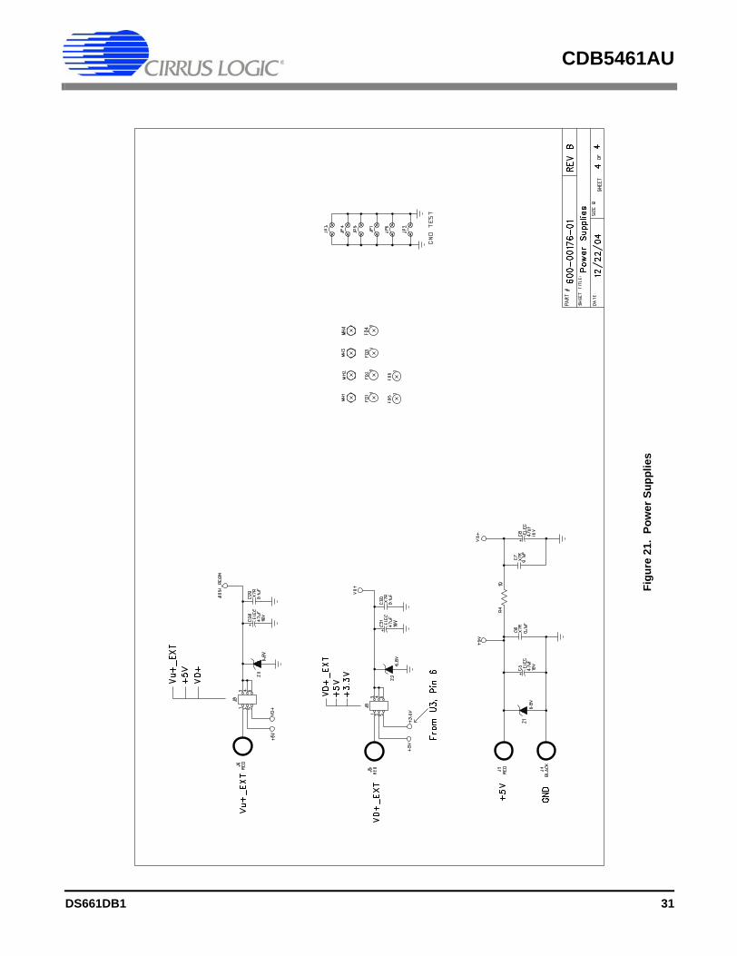
1.2.3 Power Supply Section
Table 4 illustrates the power supply connections to the evaluation board. The +5 binding post (J3) supplies the pos-itive analog (VA+) for the CS5461A and the +2.5V reference. The VD+_EXT binding post (J5) supplies the digitalsection of the CS5461A (VD+) and level shifters. Jumper J8 allows the VD+ supply to be sourced from the VD+_EXTbinding post (J5), the +5V binding post (J3), or the regulated 3.3V supply derived from the microcontroller. TheVu+_EXT (J6) binding post supplies the positive supply for the 8051 microcontroller (8051_REGIN). Jumper J9 al-lows the 8051_REGIN supply to be sourced from either the Vu+_EXT binding post (J6), +5V binding post (J3) orVD+_EXT binding post (J5).
Power Supplies Power Post Connections VD+ 8051-REGINAnalog (VA+) Digital (VD+) 8051 (Vu+) +5V GND VD+EXT VU+EXT J8 J9
+5 +5 +5 +5 0
NC
NC
+5
NC
+5
NC
+5
NC
+5 +3.3 +5 +5 0
NC
NC
+5
+3.3
NC
+5
Table 4. Power Supply Connections
O VD+O O VD+O O VD+
VD+_EXT +5 +3.3 (Default)
O 8051O O 8051O O 8051
Vu+_EXT +5 VD+ (Default)
O VD+O O VD+O O VD+
VD+_EXT +5 +3.3
O 8051O O 8051O O 8051
Vu+_EXT +5 VD+
O VD+O O VD+O O VD+
VD+_EXT +5 +3.3
O 8051O O 8051O O 8051
Vu+_EXT +5 VD+
O VD+O O VD+O O VD+
VD+_EXT +5 +3.3
O 8051O O 8051O O 8051
Vu+_EXT +5 VD+
O VD+O O VD+O O VD+
VD+_EXT +5 +3.3
O 8051O O 8051O O 8051
Vu+_EXT +5 VD+
O VD+O O VD+O O VD+
VD+_EXT +5 +3.3
O 8051O O 8051O O 8051
Vu+_EXT +5 VD+
O VD+O O VD+O O VD+
VD+_EXT +5 +3.3
O 8051O O 8051O O 8051
Vu+_EXT +5 VD+
O VD+O O VD+O O VD+
VD+_EXT +5 +3.3
O 8051O O 8051O O 8051
Vu+_EXT +5 VD+
O VD+O O VD+O O VD+
VD+_EXT +5 +3.3
O 8051O O 8051O O 8051
Vu+_EXT +5 VD+
O VD+O O VD+O O VD+
VD+_EXT +5 +3.3
O 8051O O 8051O O 8051
Vu+_EXT +5 VD+
DS661DB1 7
CDB5461AU
1.3 Auto-boot ModeWith a jumper connection on J18 (AUTO-BOOT ENABLE), the CS5461A operates in auto-boot mode and theCDB5461AU board operates in a stand-alone manner without connecting to a PC. When in auto-boot mode, a hard-ware reset (pressing on S1) will cause the CS5461A to boot up using the serial data from the serial EEPROM onthe board (U10). When the CS5461A is in auto-boot mode, the SPI connections between the microcontroller andthe CS5461A are removed and GUI software can not access the CS5461A registers and functions. The EEPROM must be programmed prior to the auto-boot sequence. When the CDB5461AU Evaluation Board issent from the factory, the EEPROM is programmed with the following CS5461A command/data sequence:
– 40 00 00 61– Set configuration Register, turn high-pass filters on, set K = 1;– 4C 00 7D 00– Set PulseRateE1,2 Register to 1000 Hz;– 74 00 00 04– Unmask bit #2 (LSD) in the Mask Register– E8– Start continuous conversion– 78 00 01 00– Write to the STOP bit in the Control Register, to terminate auto-boot sequence.
This sequence programs the CS5461A for continuous conversion mode. If voltage and current signals are appliedto the inputs, the CS5461A will issue pulses on the /E1, /E2 and /E3 pins. See the CS5460A data sheet for moredetails on auto-boot.
8 DS661DB1

CDB5461AU
2. SOFTWAREThe evaluation board comes with software and an USB cable to link the evaluation board to the PC. The evaluationsoftware was developed with Lab Windows®/CVI™, a software development package from national Instruments.The evaluation software is available for download on the Cirrus Logic web site at http://www.cirrus.com/industrial-software and was designed to run under Windows 2000™ or Windows XP®.
2.1 Installation ProcedureTo install the software, go to the Cirrus Logic web site at http://www.cirrus.com/industrialsoftware and refer to appli-cation note AN278.
2.2 Using the SoftwareBefore launching the software, check all jumper settings on the CDB5461AU evaluation board as described in sec-tion 1, and connect the board to an open USB port on the PC using the provided cable. Once the board is poweredon, the software program can be launched.
2.3 Start-Up Window
When the software is launched, the Start-Up window will appear. This window contains information concerning thesoftware’s title, revision number, copyright date, etc. See Figure 2.
Figure 2. CDB5461AU Start-up Window
At the top of the screen is a menu bar which displays user options. The menu bar has three items: Menu, Setup, andQuit. Initially Menu is disabled. After establishing a link to a data source the Menu item will become available.
DS661DB1 9

CDB5461AU
2.3.1 Setup
Setup allows user to establish a USB communication connection with CDB5461AU board or select a pre-saved datafile for further analysis.
If the USB is selected, the evaluation software will poll the CDB5461AU, verifying the serial communication link isready. At this point USB is checked indicating that the PC has successfully communicated with CDB5461AU eval-uation board, and device and micro-code version information are read from the board and displayed on the screen.See Figure 3.
Figure 3. Establishing a USB Connection
If the evaluation software is unable to establish a communication link with CDB5461AU an error message will ap-pear, indicating that the initial communication has failed. See Figure 6.
Figure 4. USB Error Message
Check to verify that the USB cable is connected properly and the power supply is on and connected properly to theCDB5461U. Reset the board (press the RESET button on the board) and try to setup USB again.
If Data from Disk is selected, a file selection window will appear as shown in Figure 5. The user can select a pre-saved data file for further analysis using time domain, FFT, and histogram plots in the Data Collection window of thesoftware.
10 DS661DB1

CDB5461AU
Figure 5. Selecting a Data File for Further Analysis
2.3.2 Quit
Quit allows the user to exit the evaluation software. Upon selecting Quit, a message windows appears that verifieswhether exiting the evaluation software is desired. See Figure 6.
Figure 6. Quit Window
DS661DB1 11

CDB5461AU
2.3.3 Menu
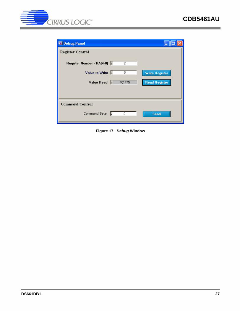
Except for the Start-up window, Menu allows 7 selection options, Setup window, Calibration window, Conversionwindow, Pulse Rate window, Data Collection window, EEPROM window and Debug window. Each window providesa means to evaluate the different functionalities and performances of the CS5461A. See Figure 7.
Figure 7. Menu Pull-down Options
2.4 Setup Window
The evaluation software provides access to the CS5461A's internal registers in the Setup window (Figure 8). Theuser can enter the Setup window by pulling down Menu and selecting the Setup Window menu item, or by pressing<F2> on the keyboard.
In the Setup window, all of the CS5461A's registers are displayed in hexadecimal notation, and also decoded to pro-vide easier readability. Refer to the CS5461A data sheet for information on register functionality and descriptions.
12 DS661DB1
CDB5461AU
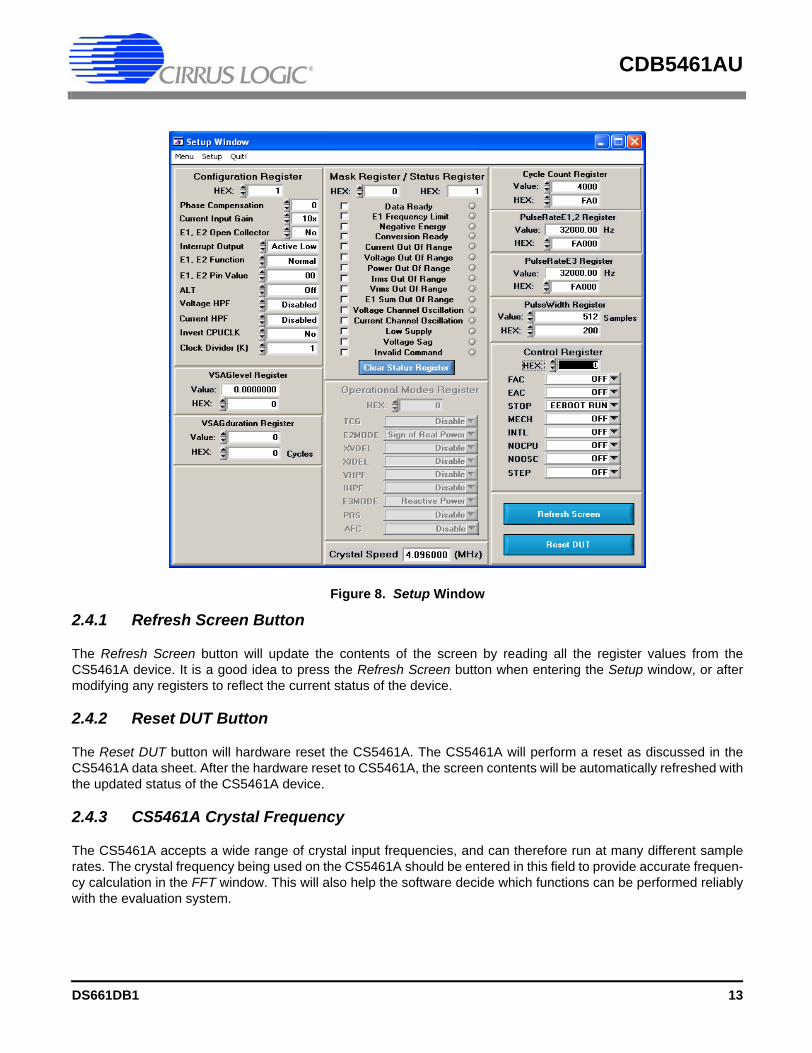
Figure 8. Setup Window
2.4.1 Refresh Screen Button
The Refresh Screen button will update the contents of the screen by reading all the register values from theCS5461A device. It is a good idea to press the Refresh Screen button when entering the Setup window, or aftermodifying any registers to reflect the current status of the device.
2.4.2 Reset DUT Button
The Reset DUT button will hardware reset the CS5461A. The CS5461A will perform a reset as discussed in theCS5461A data sheet. After the hardware reset to CS5461A, the screen contents will be automatically refreshed withthe updated status of the CS5461A device.
2.4.3 CS5461A Crystal Frequency
The CS5461A accepts a wide range of crystal input frequencies, and can therefore run at many different samplerates. The crystal frequency being used on the CS5461A should be entered in this field to provide accurate frequen-cy calculation in the FFT window. This will also help the software decide which functions can be performed reliablywith the evaluation system.
DS661DB1 13
CDB5461AU
2.4.4 Configuration Register Panel
In the Configuration Register panel, the contents of the Configuration register can be modified by typing a hexadec-imal value in the HEX: field, or by changing any of the values below the HEX: field to the desired settings. Althoughthe CDB5461AU software allows the user to modify any of the bits in the Configuration register, changing certainbits may cause the software and board to behave erratically. For the evaluation system to function properly, the In-terrupt Output field should be set to the default, Active Low setting, and E1, E2 Function field should be set to thedefault Normal. This applies only to the CDB5461AU evaluation system, and not to the CS5461A chip itself.
2.4.5 Mask Register/Status Register Panel
The Mask and Status registers are displayed in hexadecimal and decoded in this box to indicate each bit's function.The Mask register can be modified by typing a value in the HEX: field, or by checking the appropriate check boxesfor the bits that are to be masked. The Status register cannot be directly modified. It can only be reset by pressingthe Clear Status Register button. The HEX: field for this register, and the associated “lamps” are for display only. Alamp that is on means that the corresponding bit in the Status Register is set (except the Invalid Command bit, whichis inverted). The value present in the Mask register may be changed by the software during certain operations toprovide correct functionality of the CDB5461AU board.
2.4.6 Cycle Count / PulseRateE / PulseWidth / VSAGlevel / VSAGduration Registers
These fields display the values of the corresponding register in both hexadecimal and decimal format. Each registercan be modified by typing a value in the corresponding Value: or HEX: field.
2.4.7 Control Register
The Control register contains various bits used to activate or terminate various features of the CS5461A. Refer tothe CS5461A data sheet for descriptions of these bits. The user is able to set or clear each bit individually. The valueof the Control register is displayed in the HEX: field. Most of the Control register bits are reserved or unused. Onlythe usable bits are displayed in the Setup window.
14 DS661DB1

CDB5461AU
2.5 Calibration Window
The Calibration window is used to display and write to the CS5461A Offset and Gain calibration registers. The useris also able to initiate the CS5461A's calibration sequences that are used to set the calibration values. Both AC andDC calibrations can be run for offset and gain, for either the voltage channel or the current channel, or both simul-taneously. The user should refer to the CS5461A data sheet for more details on calibration.
The Refresh Screen button will update the contents of the window by reading all the register values from theCS5461A device. It is a good idea to press the Refresh Screen button when entering the Calibration window, or aftermodifying any registers to reflect the current status of the device.
Figure 9. Calibration Window
2.5.1 Offset & Gain Registers
In the Offset and Gain register panels, the offset and gain registers for both channels are displayed in hexadecimaland decimal. These registers can all be modified directly by typing the desired value in the hexadecimal displayfields. There are two types of offset registers: DC Offset and AC Offset. The AC Offset register only affects the RMSregister values. The DC and AC offset register values are two's complement numbers whose values ranges from -1 to +1.
2.5.2 Performing Calibrations
Offset and gain calibrations can be performed on both the voltage and current channels of the CS5461A. It is gen-erally a good idea to software reset the CS5461A before running calibrations because the values in the calibrationregisters will affect the results of the calibration. A software reset will reset these registers back to the default valuesof zero offset and unity gain. Offset calibration should be performed before gain calibration to ensure accurate re-sults.
DS661DB1 15

CDB5461AU
2.5.2.1 Offset Calibrations
1. Ground the channel(s) you want to calibrate directly at the channel header(s). J17 and J22 for thevoltage channel, and J24 and J26 for the current channel. The channel(s) could also be groundeddirectly at the screw terminals.
2. Press the corresponding AC or DC offset calibrate button(s) (Cal V, Cal I, or Cal Both) in the Offsetpanel.
3. The calibration value(s) will automatically update when the calibration is completed.
2.5.2.2 Gain Calibrations
1. Attach an AC or DC calibration signal to the screw terminals, and make sure the corresponding chan-nel headers (J17, J22, J24, and J26) are set to the Input position.
2. Press the corresponding AC or DC gain calibrate button(s) (Cal V, Cal I, or Cal Both) in the GainPanel.
3. The calibration value(s) will automatically update when the calibration is completed.
The Calibration window also contains the Power Offset register display and adjustment fields. The user can readand write the value in the Power Offset register.
16 DS661DB1

CDB5461AU
2.6 Conversion Window
The Conversion window shown in Figure 10 allows the user to see the results of single and continuous conversions,perform data averaging, utilize the power-saving modes of the CS5461A, and reset the CS5461A's serial port. TheConversion window can be accessed by pulling down the Menu option, and selecting Conversion Window, or bypressing <F4>.
Figure 10. Conversion Window
2.6.1 Single Conversion Button
By pressing this button, single conversions will be performed. After a single conversion is complete, the Result datacolumn will be updated with the values present in each data register.
2.6.2 Continuous Conversion Button
By pressing this button, continuous conversions will be performed until the user presses the Stop button. After eachconversion is complete, the Result data column will be updated with the values present in each data register. TheMean and Standard Deviation columns will be updated every N cycles, where N is the number in the Samples toAverage: box. It may take many collection cycles after pressing the Stop button before the data actually stops beingcollected.
2.6.3 Standby & Sleep Mode Buttons
When these buttons are pressed, the CS5461A device will enter either Standby or Sleep power-saving mode. Toreturn to normal mode, press the Power Up button.
DS661DB1 17

CDB5461AU
2.6.4 Power Up Button
This button is used to send the Power-up/Halt command to the CS5461A. The device will return to normal operatingmode and halt any conversions that are being performed at the time.
2.6.5 Temperature Settings Window
The Temperature Settings window is used to adjust the CS5461A’s Temperature Offset register (Toffset) and Tem-perature Gain register (Tgain) to convert the Temperature Register (T) from a Celsius scale (°C) to a Fahrenheit scale(°F) and to improve temperature measurement accuracy. Refer to the CS5461A data sheet for the details of the On-chip Temperature Sensor.
2.6.6 Write Data to File Window
This window provides a means to write the conversion result data to a .txt file for later analysis or print out. The filepath and name will be shown in Filename field. The Open File button is used to open a new or existing .txt file forwriting data. Each time the Write Data button is pressed, the result data is written to the file and the Number of LinesWritten field will be incremented by 1.
2.7 Pulse Rate Window
The CS5461A features a pulse-rate energy output. The CDB5461AU has the capability to demonstrate the function-ality of this output in the Pulse Rate Output window shown in Figure 11. The Pulse Rate Output window can be ac-cessed by pressing <F5>, or by pulling down Menu, and selecting Pulse Rate Window.
Figure 11. Pulse Rate Output Window
2.7.1 Integration Seconds Field
This box allows the user to select the length of time over which pulses will be collected.
2.7.2 Periods to Average Field
This box allows the user to average a number of integration periods.
18 DS661DB1

CDB5461AU
2.7.3 Start Button
When the Start button is pressed, the CDB5461AU will capture pulse rate data according to the values in the Inte-gration Seconds and Periods to Average fields. After each integration period, the Pulse Count and Frequency col-umns will be updated. The Average Freq. and Standard Deviation columns will only be updated after all theintegrations have been collected. The software stops collecting data when the user presses the Stop button, or whenthe data collection is complete. Due to speed limitations of the on-board microcontroller, some higher pulse ratescannot be accurately collected.
2.8 Data Collection Window
The Data Collection window (Figure 12, Figure 13, and Figure 14) allows the user to collect sample sets of data fromthe CS5461A and analyze them using time domain, FFT, and histogram plots. The Data Collection window is ac-cessible through the Menu pull-down, or by pressing <F6>.
Figure 12. Data Collection Window
2.8.1 Time Domain / FFT / Histogram Pull-down
This pull-down selects the type of data processing to perform on the collected data and display in the plot area. Referto the section on Analyzing Data for more information.
2.8.2 Config Button
This button will bring up the Configuration window, in which the user can modify the data collection specifications.See the discussion of the Config window in this document.
DS661DB1 19
CDB5461AU
2.8.3 Collect Button
This button will collect data from the CS5461A device to be analyzed in the plot area. See the section on CollectingData Sets for more information.
2.8.4 Output Button
This button will bring up a window in which the user can output the data to a file for later use, print out a plot, or printout the entire screen. When saving data, only the data channel being displayed on the plot will be saved to a file.
2.8.5 Zoom Button
This button allows the user to zoom in on the plot by selecting two points in the plot area. Press the Restore buttonto return to the normal data plot, or press the Zoom button again to zoom in even further.
2.8.6 Channel Select Button
After data collection, Current and Voltage channel select buttons will appear below the graph, allowing the user tochoose the appropriate channel for display. In the Time Domain mode, an additional Overlay button will be present,to allow the user to display all the channels on the same plot.
2.8.7 Config Window
The Config window allows the user to set up the data collection and analysis parameters.
2.8.7.1 Number of Samples
This field allows the user to select the number of samples to collect – between 16 and 32768.
2.8.7.2 Average
When doing FFT processing, this field will determine the number of FFTs to average. FFTs will be collected andaveraged when the Collect button is pressed.
2.8.7.3 FFT Window
This field allows the user to select the type of windowing algorithm for FFT processing. Windowing algorithms in-clude the Blackman, Blackman-Harris, Hanning, 5-term Hodie, and 7-term Hodie. The 5-term Hodie and 7-term Hod-ie are windowing algorithms developed at Crystal Semiconductor.
2.8.7.4 Histogram Bin Width
This field allows for a variable bin width when plotting histograms of the collected data. Each vertical bar in the his-togram plot will contain the number of output codes contained in this field. Increasing this number allows the user toview histograms with larger input ranges.
2.8.7.5 Data to Collect
These 3 check boxes allow the user to select the data types that will be collected and returned to the PC for pro-cessing.
20 DS661DB1

CDB5461AU
2.8.7.6 Cycle Count
The value in Cycle Count field will be written to the CS5461A’s Cycle Count register. Cycle Count determines thelength of one computation cycle. Cycle Count should be selected appropriately according to the Data to Collect se-lection. For example, if the Data to Collect is instantaneous Current, Voltage, or Power, it is better to set Cycle Countto 1. If the data to collect is RMS Current, RMS Voltage, or Average Power, Cycle Count should be set to a valuethat makes one computation cycle to be a even multiple of the line frequency.
2.8.7.7 Accept Button
When this button is pressed, the current settings will be saved, and the user will return to the Data Collection window.
2.8.8 Collecting Data Sets
To collect a sample data set:
1. In the Data Collection Window, press the Config button to bring up the Configuration Window andview the current settings.
2. Select the appropriate settings from the available options (see the section on the Configuration Win-dow) and press the Accept button.
3. The Data Collection Window should still be visible. Press the Collect button to begin collecting data.
4. Once the data has been collected, it can be analyzed, printed, or saved to disk.
2.8.9 Retrieving Saved Data from a File
The CDB5461AU software allows the user to save data to a file, and retrieve it later when needed. To load a previ-ously saved file:
1. Pull down the Setup option and select Disk. A file menu will appear.
2. Find the data file in the list and select it. Press the select button to return.
3. Go to the Data Collection Window, and press the Collect button.
4. The data from the file should appear on the screen. To select a different file, repeat the procedure.
2.8.10 Analyzing Data
The evaluation software provides three types of analysis tests: Time Domain, Frequency Domain, and Histogram.The Time Domain analysis process acquires conversions to produce a plot of magnitude versus conversion samplenumber. The Frequency Domain analysis process acquires conversions to produce a plot of magnitude versus fre-quency using the Fast-Fourier Transform (results up to Fs/2 are calculated and plotted). Also statistical noise calcu-lations are calculated and displayed. The Histogram analysis test process acquires conversions to produce ahistogram plot. Statistical noise calculations are also calculated and displayed.
DS661DB1 21

CDB5461AU
2.8.11 Histogram Information
The following is a description of the indicators associated with Histogram analysis. Histograms can be plotted in theData Collection window by setting the Time Domain / FFT / Histogram selector to Histogram (Figure 13).
Figure 13. Histogram Analysis
2.8.11.1 Bin
Displays the x-axis value of the cursor on the Histogram.
2.8.11.2 Magnitude
Displays the y-axis value of the cursor on the Histogram.
2.8.11.3 Mean
Indicator for the mean of the data sample set. The mean is calculated using the following formula:
Mean
Xii 0=
n 1–
∑n
----------------=
22 DS661DB1

CDB5461AU
2.8.11.4 STD_DEV
Indicator for the standard deviation of the collected data set. The standard deviation is calculated using the followingformula:
2.8.11.5 Variance
Indicator for the variance of the current data set. The variance is calculated using the following formula:
2.8.11.6 Maximum
Indicator for the maximum value of the collected data set.
2.8.11.7 Minimum
Indicator for the minimum value of the collected data set.
StdDev
Xi Mean–( )2
i 0=
n 1–
∑n
---------------------------------------------=
Var
Xi Mean–( )2
i 0=
n 1–
∑n
---------------------------------------------=
DS661DB1 23

CDB5461AU
2.8.12 Frequency Domain Information
The following describe the indicators associated with FFT (Fast Fourier Transform) analysis. FFT data can be plot-ted in the Data Collection window by setting the Time Domain / FFT / Histogram selector to FFT (Figure 14).
Figure 14. FFT Analysis
2.8.12.1 Frequency
Displays the x-axis value of the cursor on the FFT display.
2.8.12.2 Magnitude
Displays the y-axis value of the cursor on the FFT display.
2.8.12.3 S/PN
Indicator for the signal-to-peak noise ratio (decibels).
2.8.12.4 SINAD
Indicator for the signal-plus-noise-plus-distortion to noise-plus-distortion ratio (decibels).
2.8.12.5 S/D
Indicator for the signal-to-distortion ratio, 4 harmonics are used in the calculations (decibels).
24 DS661DB1

CDB5461AU
2.8.12.6 SNR
Indicator for the signal-to-noise ratio, first 4 harmonics are not included (decibels).
2.8.12.7 Fs-Pdb
Indicator for the full-scale to signal ratio (decibels).
2.8.13 Time Domain Information
The following controls and indicators are associated with Time Domain analysis. Time Domain data can be plottedin the Data Collection window by setting the Time Domain / FFT / Histogram selector to Time Domain (Figure 15).
Figure 15. Time Domain Analysis
2.8.13.1 Count
Displays current x-position of the cursor on the time domain display.
2.8.13.2 Magnitude
Displays current y-position of the cursor on the time domain display.
2.8.13.3 Maximum
Indicator for the maximum value of the collected data set.
DS661DB1 25

CDB5461AU
2.8.13.4 Minimum
Indicator for the minimum value of the collected data set.
2.9 EEPROM Window
CDB5461AU has an “Auto-boot” Demo feature for the serial EEPROM, which means CDB5461AU can operate in-dependently without connecting to a PC. The CDB5461AU GUI software also provides an EEPROM window forreading/writing the serial EEPROM (Figure 16).
Figure 16. EEPROM Window
The Bytes to Read/Write field allows the user to define the number of bytes to be read or written.
2.9.1 Read EEPROM
After pressing the Read button, the number of bytes indicated in the Bytes to Read/Write field, starting from address0x00 will be read from EEPROM and displayed in the EEPROM table in Hexadecimal format.
2.9.2 Write EEPROM
Starting from address 0x00, enter into the EEPROM table the bytes to be written. Pressing the Write button, thebytes in the EEPROM table will be written to the EEPROM.
2.9.3 Debug Window
The Debug window provides the user a way to access the CS5461A registers and send commands to the devicedirectly (Figure 17). Refer to the CS5461A data sheet for more details.
26 DS661DB1

CDB5461AU
Contacting Cirrus Logic SupportFor all product questions and inquiries contact a Cirrus Logic Sales Representative. To find one nearest you go to www.cirrus.comIMPORTANT NOTICECirrus Logic, Inc. and its subsidiaries ("Cirrus") believe that the information contained in this document is accurate and reliable. However, the information is subjectto change without notice and is provided "AS IS" without warranty of any kind (express or implied). Customers are advised to obtain the latest version of relevantinformation to verify, before placing orders, that information being relied on is current and complete. All products are sold subject to the terms and conditions of salesupplied at the time of order acknowledgment, including those pertaining to warranty, indemnification, and limitation of liability. No responsibility is assumed by Cirrusfor the use of this information, including use of this information as the basis for manufacture or sale of any items, or for infringement of patents or other rights of thirdparties. This document is the property of Cirrus and by furnishing this information, Cirrus grants no license, express or implied under any patents, mask work rights,copyrights, trademarks, trade secrets or other intellectual property rights. Cirrus owns the copyrights associated with the information contained herein and gives con-sent for copies to be made of the information only for use within your organization with respect to Cirrus integrated circuits or other products of Cirrus. This consentdoes not extend to other copying such as copying for general distribution, advertising or promotional purposes, or for creating any work for resale.
CERTAIN APPLICATIONS USING SEMICONDUCTOR PRODUCTS MAY INVOLVE POTENTIAL RISKS OF DEATH, PERSONAL INJURY, OR SEVERE PROP-ERTY OR ENVIRONMENTAL DAMAGE ("CRITICAL APPLICATIONS"). CIRRUS PRODUCTS ARE NOT DESIGNED, AUTHORIZED OR WARRANTED FOR USEIN AIRCRAFT SYSTEMS, MILITARY APPLICATIONS, PRODUCTS SURGICALLY IMPLANTED INTO THE BODY, AUTOMOTIVE SAFETY OR SECURITY DE-VICES, LIFE SUPPORT PRODUCTS OR OTHER CRITICAL APPLICATIONS. INCLUSION OF CIRRUS PRODUCTS IN SUCH APPLICATIONS IS UNDERSTOODTO BE FULLY AT THE CUSTOMER'S RISK AND CIRRUS DISCLAIMS AND MAKES NO WARRANTY, EXPRESS, STATUTORY OR IMPLIED, INCLUDING THEIMPLIED WARRANTIES OF MERCHANTABILITY AND FITNESS FOR PARTICULAR PURPOSE, WITH REGARD TO ANY CIRRUS PRODUCT THAT IS USEDIN SUCH A MANNER. IF THE CUSTOMER OR CUSTOMER'S CUSTOMER USES OR PERMITS THE USE OF CIRRUS PRODUCTS IN CRITICAL APPLICA-TIONS, CUSTOMER AGREES, BY SUCH USE, TO FULLY INDEMNIFY CIRRUS, ITS OFFICERS, DIRECTORS, EMPLOYEES, DISTRIBUTORS AND OTHERAGENTS FROM ANY AND ALL LIABILITY, INCLUDING ATTORNEYS' FEES AND COSTS, THAT MAY RESULT FROM OR ARISE IN CONNECTION WITHTHESE USES.
Cirrus Logic, Cirrus, and the Cirrus Logic logo designs are trademarks of Cirrus Logic, Inc. All other brand and product names in this document may be trademarksor service marks of their respective owners.Windows, Windows 2000, and Windows XP are registered trademarks of Microsoft Corporation.SPI is a trademark of Motorola, Inc.CVI is a trademark of National Instruments Corporation.
36 DS661DB1