Carbon Nanotubes and Silver Grids Hybrid Solution ... · Solution-Processed Flexible Transparent...
14
1 Supporting Information Solution-Processed Flexible Transparent Conductors Based on Carbon Nanotubes and Silver Grids Hybrid Jing Wang, Jintao Zhang, Ashok Kumar Sundramoorthy, Peng Chen*, Mary B. Chan-Park* Experimental section Materials The Ag-PET films were obtained from Cima NanoTech and used as received. The P2- SWNTs were purchased from Carbon Solutions and used as received. All other chemicals were purchased from Sigma and used as received. Deionized water (D. I. water) was used in all experiments. Fabrication of SWNT-Ag-PET hybrid electrodes 10 mg P2-SWNTs were mixed with 10 mL of 1 mgmL -1 sodium cholate (SC) aqueous solution. The mixture was ultrasonicated using a 130-Watt Ultrasonic Processor (VCX130, Sonics & Materials, Inc., USA) for 1 hr (60% amplitude). The suspension was then centrifuged at 50,000 g for 1 hr. The top 80% supernatant was carefully removed and diluted 10-fold with 1% SC solution. The diluted solution was bath-sonicated for 10 min before use. The as-received Cima Ag-PET film was covered with sacrificial thin PET layers, front (the side with Ag grid) and back (the side without Ag grid). The front sacrificial PET layer was removed before any surface treatment of the Ag network side of the film, while the back layer was kept in place during all processing steps to avoid any contamination to the back side. The back sacrificial layer was removed before characterization or use. The front sacrificial plain PET layer on the Ag-PET was removed, and the Ag-PET films were exposed to Ar plasma for 60 s at 100W power. Then the films were immersed in 0.5 vol.% of (3-Aminopropyl)triethoxysilane (APTES) solution in ethanol for 45 min. The excess Electronic Supplementary Material (ESI) for Nanoscale. This journal is © The Royal Society of Chemistry 2014
Transcript of Carbon Nanotubes and Silver Grids Hybrid Solution ... · Solution-Processed Flexible Transparent...

1
Supporting Information
Solution-Processed Flexible Transparent Conductors Based on Carbon Nanotubes and Silver Grids Hybrid
Jing Wang, Jintao Zhang, Ashok Kumar Sundramoorthy, Peng Chen*, Mary B. Chan-Park*
Experimental section
Materials
The Ag-PET films were obtained from Cima NanoTech and used as received. The P2-
SWNTs were purchased from Carbon Solutions and used as received. All other chemicals
were purchased from Sigma and used as received. Deionized water (D. I. water) was used in
all experiments.
Fabrication of SWNT-Ag-PET hybrid electrodes
10 mg P2-SWNTs were mixed with 10 mL of 1 mgmL-1 sodium cholate (SC) aqueous
solution. The mixture was ultrasonicated using a 130-Watt Ultrasonic Processor (VCX130,
Sonics & Materials, Inc., USA) for 1 hr (60% amplitude). The suspension was then
centrifuged at 50,000 g for 1 hr. The top 80% supernatant was carefully removed and diluted
10-fold with 1% SC solution. The diluted solution was bath-sonicated for 10 min before use.
The as-received Cima Ag-PET film was covered with sacrificial thin PET layers, front (the
side with Ag grid) and back (the side without Ag grid). The front sacrificial PET layer was
removed before any surface treatment of the Ag network side of the film, while the back layer
was kept in place during all processing steps to avoid any contamination to the back side. The
back sacrificial layer was removed before characterization or use.
The front sacrificial plain PET layer on the Ag-PET was removed, and the Ag-PET films
were exposed to Ar plasma for 60 s at 100W power. Then the films were immersed in 0.5
vol.% of (3-Aminopropyl)triethoxysilane (APTES) solution in ethanol for 45 min. The excess
Electronic Supplementary Material (ESI) for Nanoscale.This journal is © The Royal Society of Chemistry 2014

2
APTES was rinsed away with ethanol. The films were rinsed with D.I. water and blown dry
with compressed air. Then the APTES-treated Ag-PET films were immersed in the diluted
SWNT dispersion for 1 h. After immersion, the hybrid films were rinsed with D.I. water and
blown dry. The films were dried at 70oC overnight before characterization. The preparation of
the control SWNT-PET samples followed the same procedure except that the plain PET film
was purchased from Higashiyama Film (Singapore).
Fabrication of graphene-Ag-PET hybrid electrodes
Graphene was synthesized via an optimized atmospheric chemical vapor deposition (CVD)
method. Copper foil (99.8%, 25 µm thick) was purchased from Alfa Aesar and cut into pieces
of the desired size. The copper foil pieces were carefully rolled and transferred into a quartz
tube with inner diameter of 22 mm. The tube was purged with 500 sccm Ar for 20 min, and
then heated to 925 oC in a split tube furnace. 60 sccm H2 was introduced during the heating
process. The system was kept at 925oC for several minutes to reduce the surface oxidation of
copper foils. Ar was cut off and 5 sccm CH4 was introduced for 5 min while H2 was kept at 60
sccm. After 5 min, during which graphene was grown, the CH4 was cut off and Ar was
introduced again in the cooling stage.
The synthesized graphene was transferred by an improved wet transfer process. While still
on the copper foils, the graphene was protected by application of a sacrificial poly(methyl
methacrylate) (PMMA) layer. The copper foils were then etched away with Fe(NO3)3
solution. After removal of the copper, the graphene films were rinsed with D.I. water several
times and transferred onto Ag-PET films. The film (with its PMMA sacrifice layer) was
exposed under UV light for 10 min to degrade the PMMA into methyl methacrylate
monomers which were then removed with acetone.

3
Fabrication of met-SWNT-Ag-PET hybrid electrodes
99% met-SWNTs solution was purchased from NanoIntegris and diluted with D.I. water.
The diluted solution was bath-sonicated for 10 min and vacuum filtered through 0.2 µm pore
size PTFE membrane (diameter 47 mm). The met-SWNTs film on PTFE membrane was then
washed with D.I. water and directly transferred onto Ag- PET film with a laminator at 130 oC.
Electrochemical deposition of ZnO
ZnO nanosheets were electrodeposited on a PET/Ag/CNT substrate (1 cm × 2 cm) in a
three-electrode cell with the PET/Ag/CNT as working electrode, a Pt plate as counter
electrode, and a Ag/AgCl (sat. KCl) electrode as reference electrode. The electrolyte
contained 50 mL of 0.05 M ZnCl2 and 0.5 M KCl. The deposition was performed at –1.0 V
for 1 h at room temperature.
Measurement of photocurrent
The photocurrent was measured on an electrochemical workstation (CHI660c, CH
Instruments) with a three-electrode configuration. The as-prepared sample, Pt-wire electrode,
and Ag/AgCl electrode were employed as the working, counter, and reference electrodes,
respectively. The samples were illuminated by a Xenon-lamp light source (100 mW cm-2) at
the open circuit potential. 0.5 M Na2SO4 solution was used as the electrolyte.
Characterizations
The sheet resistance was measured with a Keithlink four-point probe station (probe spacing
1.6 mm, probe pin diameter 40.6µm.). Scanning electron microscopy (SEM) was performed
using LEO 1550 Gemini field-emission scanning electron microanalyzer at an accelerating
voltage of 5 kV. The ZnO-SWNT-Ag-PET sample was coated with Pt for 10 seconds under
acurrent of 10 mA. All the other samples were scanned directly, without Pt coating. Raman
spectroscopy was conducted using a Renishaw inVia Raman microscope with 514.5 nm (2.41

4
eV) laser wavelength in a backscattering configuration. UV-vis-NIR absorption spectra were
measured using a Varian Cary 5000 UV-vis-NIR spectrophotometer. The substrate absorption
for background subtraction was measured using a blank PET substrate. X-ray diffraction
(XRD) patterns were recorded on a Bruker AXS D8 Advance, equipped with a Cu Kα photon
source (40 kV, 20 mA, λ=0.15406 nm) scanned at the rate of 1.0o min-1 over the range 32o-80o
(2θ).

5
Figure S1. A) SEM image of SWNT network thin film on Ag-PET. B) High magnification
SEM image of the SWNT network thin film in the empty area, marked with red square in A).

6
Figure S2. Gross visual appearance and transparency of SWNT-Ag-PET film (16cm ×12cm
sample).The red arrows show the boundary between the regions with (left) / without (right)
SWNT network thin film.

7
Figure S3. A) Schematic of the four-point probe configuration (not to scale).The probe
spacing is 1.6 mm and the probe pin diameter is 40.6µm. B) Optical microscope image of the
Ag-PET film. Some branches of the Ag-grids are highlighted in red circles.

8
1000 2000 3000
2D
Inte
nsity
(a.u
.)
Raman Shift (cm-1)
G
B
500nm
DGraphene-Ag-PET
Ag-PET
C
A
Graphenewrinkle
Figure S4. A) Visual appearance of graphene-Ag-PET hybrid film (9.5 cm × 5 cm sample).
The blue arrows show the boundary between the regions with (bottom) /without (top)
graphene. B) Raman spectrum of graphene used in this work. C) Optical microscope image of
a graphene-Ag-PET film. Graphene covers the top part of the image, indicated by the white
dashed line. D) SEM image of graphene-Ag-PET film in the red square of C).
9
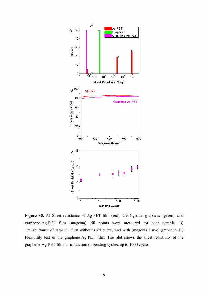
Figure S5. A) Sheet resistance of Ag-PET film (red), CVD-grown graphene (green), and
graphene-Ag-PET film (magenta). 50 points were measured for each sample. B)
Transmittance of Ag-PET film without (red curve) and with (magenta curve) graphene. C)
Flexibility test of the graphene-Ag-PET film. The plot shows the sheet resistivity of the
graphene-Ag-PET film, as a function of bending cycles, up to 1000 cycles.

10
Figure S6. A) Optical microscopy image of Ag-PET with (top) and without (bottom) thin
film of met-SWNTs network. B)A SEM image of met-SWNTs-Ag-PET hybrid film in the red
square of A). C) Visual appearance of a met-SWNTs-Ag-PET film. The met-SWNTs film
was prepared by vacuum filtration on PTFE membrane (47 mm diameter) and then transferred
onto the Ag-PET film.

11
Figure S7. A) Sheet resistance of Ag-PET film (red), met-SWNTs network (green) and met-
SWNTs-Ag-PET film (dark cyan). 50 points were measured for each sample. B)
Transmittance of Ag-PET film without (red curve) and with (dark cyan curve) met-SWNT
network thin film. The absorbance peak between ~600-800 nm is attributed to the M11
transitions of met-SWNTs. C) Flexibility test of the met-SWNT-Ag-PET film. The plot shows
the sheet resistivity of the met-SWNT-Ag-PET film, as a function of bending cycles, up to
1000 cycles.

12
Figure S8. A) SEM image of SWNT-Ag-PET hybrid film before bendability test. B)* High
magnification SEM image of pre-bending SWNT-Ag-PET hybrid film, marked with red
square in A). C) SEM image of SWNT-Ag-PET hybrid film after bendability test (1000
cycles), showing no machenical degradation of Ag nanoparticles or thin film of SWNT
network after 1000 cycles of bendability test. D) High magnification SEM image of pre-
bending SWNT-Ag-PET hybrid film, marked with red square in C). * Figure S8-B is the same figure as Figure 1F.

13
Table S1. Sheet resistance and transmittance of SWNT-Ag hybrid hybrid electrode (No. 1)
graphene-Ag hybrid electrode (No. 2) and met-SWNT-Ag hybrid (No. 3) compared to
commercial transparent electrode materials and previous research results (No. 4-18).
No. Product Substrate Sheet Resistance (Transmittance)a) σDC/σOp
1 SWNT-Ag hybrid (this work) PET 5.8±1.1 Ω sq-1 (83.7%) 349
2 graphene-Ag hybrid (this work) PET 5.6±0.6 Ω sq-1 (82.3%) 329
3 met-SWNT-Ag hybrid (this work) PET 6.1±0.4 Ω sq-1 (82.0%) 296
4 ITO glass 30-80 Ω sq-1 (90%) 44-116
5 PEDOT/PSS[1] glass/PET 100 Ω sq-1 (91%) 39
6 SWNTs[2] PET 60 Ω sq-1 (90%) 58
7 graphene[3] glass 350 Ω sq-1 (90%) 10
8 graphene/SWNTs[4] glass 280 Ω sq-1 (86%) 9
9 Cu nanofibers[5]b) glass 12 Ω sq-1 (80%) 133
10 Ag nanowires[6] PET 13 Ω sq-1 (85%) 171
11 graphene[7] (doped by AuCl3) glass 150 Ω sq-1 (87%) 17
12 graphene[8] (doped by AuCl3) PET 54 Ω sq-1 (85%) 41
13 graphene[9] (doped by HNO3) PET 30 Ω sq-1 (90%) 116
14 Cu grid-Ni thin film hybrid[10] fused silica 6.5 Ω sq-1 (75%) 187
15 Cu-Ti bilayer thin film[11] fused silica 16 Ω sq-1 (86%)c) 150
16 graphene-Au gridd) hybrid[12] glass 4±1 Ω sq-1 (79%) / 20±4 Ω sq-1 (91%) 377/195
17 graphene-Al gride) hybrid[12] PET 18±9 Ω sq-1 (79%) / 60±15 Ω sq-1 (91%) 84/65
18 graphene-Cu gride) hybrid[12] PET 8±3 Ω sq-1 (79%) / 30±6 Ω sq-1 (91%) 188/130
a)Transmittance of all the electrodes (except No. 15c)) was measured at 550 nm (substrate
absorption substracted). b)Copper nanofibers were prepared by electrospinning. c)Transmittance at 630 nm. d)The metal grids were prepared by sputtering. e)The metal grids
were prepared by thermal evaporation.

14
References
[1] A. Elschner, W. Lovenich, MRS Bull.2011, 36, 794.[2] D. S. Hecht, A. M. Heintz, R. Lee, L. B. Hu, B. Moore, C. Cucksey, S. Risser, Nanotechnology2011, 22, 075201.[3] X. S. Li, Y. W. Zhu, W. W. Cai, M. Borysiak, B. Y. Han, D. Chen, R. D. Piner, L. Colombo, R. S. Ruoff, Nano Lett.2009, 9, 4359.[4] V. C. Tung, L. M. Chen, M. J. Allen, J. K. Wassei, K. Nelson, R. B. Kaner, Y. Yang, Nano Lett.2009, 9, 1949.[5] H. Wu, L. B. Hu, M. W. Rowell, D. S. Kong, J. J. Cha, J. R. McDonough, J. Zhu, Y. A. Yang, M. D. McGehee, Y. Cui, Nano Lett.2010, 10, 4242.[6] S. De, T. M. Higgins, P. E. Lyons, E. M. Doherty, P. N. Nirmalraj, W. J. Blau, J. J. Boland, J. N. Coleman, ACS Nano2009, 3, 1767.[7] K. K. Kim, A. Reina, Y. M. Shi, H. Park, L. J. Li, Y. H. Lee, J. Kong, Nanotechnology2010, 21, 285205.[8] F. Gunes, H. J. Shin, C. Biswas, G. H. Han, E. S. Kim, S. J. Chae, J. Y. Choi, Y. H. Lee, ACS Nano2010, 4, 4595.[9] S. Bae, H. Kim, Y. Lee, X. F. Xu, J. S. Park, Y. Zheng, J. Balakrishnan, T. Lei, H. R. Kim, Y. I. Song, Y. J. Kim, K. S. Kim, B. Ozyilmaz, J. H. Ahn, B. H. Hong, S. Iijima, Nat. Nanotechnol.2010, 5, 574.[10] D. S. Ghosh, T. L. Chen, V. Pruneri, Appl. Phys. Lett.2010, 96, 041109.[11] D. S. Ghosh, T. L. Chen, V. Pruneri, Appl. Phys. Lett.2010, 96, 091106.[12] Y. Zhu, Z. Z. Sun, Z. Yan, Z. Jin, J. M. Tour, ACS Nano2011, 5, 6472.