Camera System Design
67
Camera System Design Examensarbete utfört i Elektroniksystem av Robert Risberg LiTH-ISY-EX-3129-2003 Linköping 2003
Transcript of Camera System Design
Camera System Design
Examensarbete utfört i Elektroniksystem av
Robert Risberg
LiTH-ISY-EX-3129-2003 Linköping 2003

Camera System Design
M.Sc. Thesis performed for the Division of Electronics System at Linköping Institute of Technology
Robert Risberg
Reg nr: LiTH-ISY-EX-3129-2003
Supervisor: Jan Svensson
Examiner:
Kent Palmkvist
Linköping, November 17th 2003

Avdelning, Institution Division, Department
Institutionen för Systemteknik 581 83 LINKÖPING
Datum Date 2003-11-17
Språk Language
Rapporttyp Report category
ISBN
Svenska/Swedish X Engelska/English
Licentiatavhandling X Examensarbete
ISRN LITH-ISY-EX-3129-2003
C-uppsats D-uppsats
Serietitel och serienummer Title of series, numbering
ISSN
Övrig rapport ____
URL för elektronisk version http://www.ep.liu.se/exjobb/isy/2003/3129/
Titel Title
Camera System Design
Författare Author
Robert Risberg
Sammanfattning Abstract Devices have become increasingly more interconnected to their surroundings over the last few years. The introduction of Bluetooth is likely to further accelerate this trend. With Bluetooth’s bandwidth and expected low price, many devices will likely be fitted with Bluetooth chips and thus enable more devices to exchange data. This master thesis aims at connecting a Personal Digital Assistant to an ARM Thumb microcontroller over Bluetooth. To the ARM Thumb shall an image capturing device be interfaced and the captured images shall be sent over Bluetooth to the Personal Digital Assistant which shall display them.
Nyckelord Keyword Image sensor, hardware implementation, software implementation, run-length compression

Abstract i
Abstract
Devices have become increasingly more interconnected to their surroundings over the last few years. The introduction of Bluetooth is likely to further accelerate this trend. With Bluetooth’s bandwidth and expected low price, many devices will likely be fitted with Bluetooth chips and thus enable more devices to exchange data. This master thesis aims at connecting a Personal Digital Assistant to an ARM Thumb microcontroller over Bluetooth. To the ARM Thumb shall an image capturing device be interfaced and the captured images shall be sent over Bluetooth to the Personal Digital Assistant which shall display them.

ii Abstract
Preface iii
Preface
This thesis presents the design and implementation of a camera system performed at, and for, TietoEnator Embedded Tech AB, Gothenburg, during the summer and fall of 2000.
Emphasis is put on describing the path followed through the project, why certain solutions were preferred over others and how they were implemented rather than sidetracks and alternative solutions investigated. Practical problems experienced will not be discussed in the thesis nor work which did not directly have an impact on the end product. Acknowledgments
The work this thesis is derived from was facilitated by help and contributions from the following people; Stefan Bryne, Lars Pensjö, Rikard Johansson. Many helpful suggestions regarding the language in this thesis was provided by Lisa George-Svahn. Numerous comments regarding the content of the thesis was provided by Björn Olsson. This thesis was produced with LaTeX and Microsoft Word. All figures have been drawn with xfig and charts have been plotted with gnuplot.

iv Preface
Notation v
Notation
All abbreviations are written out either in brackets or in a footnote the first time they are being used. Trademark, Copyright and All Rights Reserved symbols are only written out the first time their corresponding names are used. In the report PDA [Personal Digital Assistant] will be used interchangeably with handheld device or simply handheld and greyscales will denote shades of grey.
Abbreviations
bps bits per second CPU Central Processing Unit DCE Data Communication Equipment DTE Data Terminal Equipment EBI External Bus Interface EBSK Ericsson Bluetooth Starter Kit fps frames per second GUI Graphical User Interface HCI Host Controller Interface ICE In Circuit Emulation I/O Input/Output JVM Java Virtual Machine LZW Lempel-Ziv-Welsh MOPS Millions of Operations Per Second nop no operation OS Operating System PCB Printed Circuit Board PDA Personal Digital Assistent RAM Random Access Memory RGB Red Green Blue RISC Reduced Instruction Set Computer RT Real-Time RTOS Real-Time Operating System SCCB Serial Camera Control Bus USART Universal Synchronous/Asynchronous Receiver/Transmitter USB Universal Serial Bus

vi Notation
Contents vii
Contents
1 Introduction ..............................................................................................................1 1.1 Problem Specification.......................................................................................1 1.2 Objectives .........................................................................................................1 1.3 Limitations........................................................................................................1 1.4 Methods ............................................................................................................1 1.5 Reader’s Guide .................................................................................................1 1.6 Thesis Outline...................................................................................................2
2 Background ..............................................................................................................3 2.1 Start of Project ..................................................................................................3
3 Problem Analysis .....................................................................................................5 3.1 Throughput .......................................................................................................5
3.1.1 Bluetooth Modules ....................................................................................5 3.1.2 Serial Ports ................................................................................................5 3.1.3 Compression..............................................................................................5 3.1.4 Compression Tradeoffs .............................................................................6
3.2 Budget...............................................................................................................7 3.3 Information .......................................................................................................7
4 Hardware ..................................................................................................................9 4.1 Atmel’s evaluation board..................................................................................9 4.2 Ericsson Bluetooth Modules.............................................................................9 4.3 Colour ...............................................................................................................9 4.4 Resolution .......................................................................................................10 4.5 Choosing PDA................................................................................................11 4.6 Image Capturing Device .................................................................................12
4.6.1 Photobit PB-0100 / PB-0101 Image Sensor............................................13 4.7 Bluetooth to PDA Interface ............................................................................14 4.8 Image Sensor to Evaluation Board Interface ..................................................15
4.8.1 Trigger Signal..........................................................................................15 4.8.2 Clocking ..................................................................................................17 4.8.3 Bus Interface ...........................................................................................17 4.8.4 I2C interface ............................................................................................17 4.8.5 Power Supply ..........................................................................................18 4.8.6 PB-0101...................................................................................................18
5 Software .................................................................................................................19 5.1 Reading the Input............................................................................................19 5.2 Storing the Data ..............................................................................................20 5.3 Checking the Frame Integrity .........................................................................21 5.4 Processing the Image Data..............................................................................21 5.5 Compressing the Image Data..........................................................................23 5.6 Program Structure - Image Sensor Side..........................................................24 5.7 Displaying Graphics .......................................................................................25 5.8 Decompressing the Image Data ......................................................................25 5.9 Program Structure - PDA Side .......................................................................27
6 Communication ......................................................................................................29 6.1 The Grey Boxes - Serial Communication.......................................................29
6.1.1 Verification .............................................................................................29
viii Contents
6.2 The Grey Boxes - Bluetooth Communication ................................................30 7 Results ....................................................................................................................33
7.1 Serial Link Results..........................................................................................33 7.2 Bluetooth Results............................................................................................34
8 Discussion ..............................................................................................................35 8.1 The Project in General ....................................................................................35 8.2 Tools ...............................................................................................................35 8.3 PDA ................................................................................................................35 8.4 Bluetooth.........................................................................................................35 8.5 Compression Algorithm..................................................................................35 8.6 Image sensor ...................................................................................................36 8.7 Conclusions.....................................................................................................36
References....................................................................................................................37 Appendix A: Lena......................................................................................................39 Appendix B: Schematics ...........................................................................................41 Appendix C: Importance of compression algorithm .................................................43 Appendix D: I2C ........................................................................................................47 Appendix E: Run-length compression ......................................................................49
Contents ix
List of Figures
Figure 3.1. Throughput increased by compression........................................................6 Figure 4.1. The renowned greyscale image Lena. .......................................................10 Figure 4.2. DCE side behind a D-Sub 9 female connector..........................................14 Figure 4.3. Image sensor output...................................................................................16 Figure 4.4. Relationship between pixel output, pixel clock and line valid signals ......16 Figure 4.5. Relationship between frame valid and line valid signals ..........................16 Figure 4.6. JK flip-flops signals...................................................................................17 Figure 5.1. Problem with sampling on uneven intervals .............................................20 Figure 5.2. Output from the image sensor and the sampled data.................................21 Figure 5.3. Image sensor output data ...........................................................................22 Figure 5.4. Greyscale conversion difficulties ..............................................................22 Figure 5.5. Byte usage in run-length compression ......................................................24 Figure 5.6. Program flow on image sensor side...........................................................25 Figure 5.7. Program structure on PDA side.................................................................28 Figure 6.1. Modified stop-and-wait protocol ...............................................................30 Figure 6.2. Bluetooth stack ..........................................................................................31 Figure 7.1. Captured scene 1........................................................................................33 Figure 7.2. Captured scene 2........................................................................................34 Figure C.1 The relationship between IA, B and RA.......................................................44 Figure C.2 The relationship between IA and RA at 57,600 bps.....................................44 List of Tables
Table 4.1. Handheld candidates ...................................................................................12 Table 4.2. Image sensor candidates .............................................................................13 Table 4.3. DCE to DCE converter ...............................................................................15 Table 5.1. Critical code for reading and storing pixel values ......................................20 Table 5.2. Source code for colour to greyscale conversion .........................................23 Table 5.3. Source code for run-length compression ....................................................24 Table 5.4. Source code for Palm Vx run-length decompression .................................27

x Contents
1 Introduction 1
1 Introduction
Devices have become increasingly more interconnected to their surroundings over the last few years. With the introduction of Bluetooth® this trend is likely to further increase the level of interconnectivity between new devices, thus will pose new requirements on the designs to enable connectivity to various wireless networks. This thesis was based on a project which aimed at connecting a PDA [Personal Digital Assistant] to an ARM® Thumb® microcontroller over Bluetooth and interface necessary hardware to build a wireless camera system.
1.1 Problem Specification
To capture video or still images from a camera or an image sensor, transmit the data over Bluetooth to a PDA and to finally display the images on the PDA. The image capturing hardware should be interfaced to an ARM Thumb microcontroller on an Atmel® evaluation board.
1.2 Objectives
Three objectives would set the design guidelines: 1. To design and build a visually impressive system using a minimal amount of
hardware. 2. To maximize throughput over the Bluetooth link. 3. To design the ARM Thumb side software for running under a RTOS [Real-
Time Operating System].
1.3 Limitations
The thesis only describes the path to the final product. Which decisions were made and why will be discussed but alternative solutions and sidetracks followed will be excluded. Work done by others on which the final application relied upon will be described to such extent that major functionality is covered whereas inner workings will not be included.
1.4 Methods
Literature has been read to support design decisions but the final results has been reached through practical work, multiple implementations, various system tests and optimisations to see which alternatives were feasible and which were not.
1.5 Reader’s Guide
The different problems encountered during the implementation of the system are described in this thesis as well as how they were solved. During the project many different areas were worked on simultaneously in order to minimize time lost due to delays from third parties. In this thesis, however, the design process have been structured into different sections for readability reasons. What is not included is full source code or PCB [Printed Circuit Board] layout since the purpose of this paper is
2 1 Introduction
not to constitute a blueprint for a wireless camera application, but rather serve as a documentation of the work performed.
1.6 Thesis Outline
The thesis comprise five different sections: Background, what was the purpose of the project. Problem analysis, what problems could be encountered in the project. Hardware, what solutions were employed and why. Software, what solutions were employed and why. Final results and discussion, achieved results and criticism.
2 Background 3
2 Background
TietoEnator Embedded Tech AB has traditionally focused on embedded RT [Real-Time] systems. To broaden and demonstrate their competence in Bluetooth, the company set up three different master thesis projects which together would create a wireless demonstration application.
The first project’s goal was to port a Bluetooth stack to the ARM Thumb microcontroller and get the same stack to work under Linux®. The project also included hardware design to interface electric engines and sensors, available from Lego® MindstormsTM, to the ARM Thumb microcontroller.
The aim of the second project was to get WxWorks®’ RTOS [Real-Time Operating System] Tornado® to run on the Atmel evaluation board along with WxWorks’ JVM [Java Virtual Machine]. This would in the end enable a user to, through a front-end such as a web page, download programs and/or send commands over Bluetooth to the ARM Thumb microcontroller.
The third project’s goal, this project, was according to the problem specifications in section 1.1 to interface an image capturing device to the ARM Thumb microcontroller, send information over Bluetooth to a PDA and provide a demonstration application. The Bluetooth stack, from the first project, should be ported to the PDA and interfaced with the existing TCP/IP implementation in the PDA’s OS.
The final product would be a wireless lego car fitted with sensors and a camera which would broadcast the camera’s field of view to a PDA and/or a website. The car would be controlled from the PDA or have pre-programmed instructions downloaded from the web. When the different projects had merged the hardware could be redesigned, omitting unnecessary components, and shrunk to minimize the car. This was also the reason for the three different project to work on the same evaluation boards, for the software to be adapted to a RTOS environment and for minimizing the hardware used.
2.1 Start of Project
No specifications on performance were given at the start of the project and no development software were set up nor decided upon. Bluetooth modules from EBSK [Ericsson Bluetooth Starter Kit] and Atmel’s evaluation board had been purchased but the other hardware would be chosen after a problem analysis. There were ideas about using Nintendo®’s Game Boy® camera for capturing images and to use a handheld device from PalmTM as PDA since developer tools for Palm OS® were already available.

4 2 Background
3 Problem Analysis 5
3 Problem Analysis
A problem analysis was undertaken in order to determine the theoretical limitations of the system. The problem analysis would also serve as a pre-study of attainable capacities in the system.
3.1 Throughput
In the data path, from camera lens to PDA, many potential problems could arise which had to be taken into consideration when designing the system. The most serious aspect was the existence of bottlenecks in the data path, which would ultimately set the throughput.
3.1.1 Bluetooth Modules
The Bluetooth modules from EBSK were, with the original firmware and hardware, limited to bitrates of 56,700 bps. According to the v1.0 Bluetooth specifications [1] the Bluetooth chip would reach throughputs of 723,200 bps and thus the bottleneck would be eliminated in time.
3.1.2 Serial Ports
The Bluetooth modules were fitted with both a RS-232 serial port and an USB [Universal Serial Bus] port. The evaluation board from Atmel [2] only supported RS-232 serial ports. The RS-232 controller chip on the Atmel evaluation board was estimated to be able to handle a minimum of 115,200 bps in its serial communication. PDAs were assumed to support the same bitrates since their intended serial hosts are PCs which are capable of serial communication at 115,200 bps and possibly more. The maximum attainable data rate was thus assumed to be anywhere from 115,200 bps to Bluetooth’s maximum of 723,200 bps. The system design was made with this in mind although calculation in this thesis uses the lower bandwidth of 115,200 bps.
3.1.3 Compression
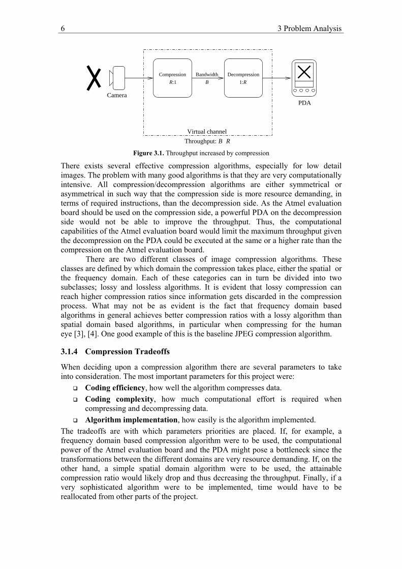
The throughput could however be increased with the use of compression. By compressing the data before sending it through the bottleneck and decompressing it when through the bottlenecks, the throughput could in theory be increased to the product of the bandwidth, B, and the achieved image compression ratio, R, as shown in Figure 3.1.
6 3 Problem Analysis
RBThroughput:
CameraPDA
Virtual channel
Compression
:1R
Decompression
1:R
Bandwidth
B
Figure 3.1. Throughput increased by compression
There exists several effective compression algorithms, especially for low detail images. The problem with many good algorithms is that they are very computationally intensive. All compression/decompression algorithms are either symmetrical or asymmetrical in such way that the compression side is more resource demanding, in terms of required instructions, than the decompression side. As the Atmel evaluation board should be used on the compression side, a powerful PDA on the decompression side would not be able to improve the throughput. Thus, the computational capabilities of the Atmel evaluation board would limit the maximum throughput given the decompression on the PDA could be executed at the same or a higher rate than the compression on the Atmel evaluation board.
There are two different classes of image compression algorithms. These classes are defined by which domain the compression takes place, either the spatial or the frequency domain. Each of these categories can in turn be divided into two subclasses; lossy and lossless algorithms. It is evident that lossy compression can reach higher compression ratios since information gets discarded in the compression process. What may not be as evident is the fact that frequency domain based algorithms in general achieves better compression ratios with a lossy algorithm than spatial domain based algorithms, in particular when compressing for the human eye [3], [4]. One good example of this is the baseline JPEG compression algorithm.
3.1.4 Compression Tradeoffs
When deciding upon a compression algorithm there are several parameters to take into consideration. The most important parameters for this project were:
Coding efficiency, how well the algorithm compresses data. Coding complexity, how much computational effort is required when
compressing and decompressing data. Algorithm implementation, how easily is the algorithm implemented.
The tradeoffs are with which parameters priorities are placed. If, for example, a frequency domain based compression algorithm were to be used, the computational power of the Atmel evaluation board and the PDA might pose a bottleneck since the transformations between the different domains are very resource demanding. If, on the other hand, a simple spatial domain algorithm were to be used, the attainable compression ratio would likely drop and thus decreasing the throughput. Finally, if a very sophisticated algorithm were to be implemented, time would have to be reallocated from other parts of the project.
3 Problem Analysis 7
3.2 Budget
The project had a small budget, therefore costs had to be kept to a minimum. This could reflect on development systems, both hardware and software, and hardware components which ultimately results in longer development times.
3.3 Information
Other problems related to the implementation of the system, but not directly affecting its properties, could be obtaining technical datasheets, application notes and technical support for new hardware. The difficulties for software could be the obtaining of development system’s documentation, standards, and documentation to closed source software interfaces.

8 3 Problem Analysis
4 Hardware 9
4 Hardware
At the beginning of the project the microcontroller to be used, along with the Bluetooth modules, had already been decided upon. In order to choose and interface the remaining hardware for the system the capabilities and limitations of the pre-chosen hardware had to be investigated.
4.1 Atmel’s evaluation board
The AT91EB01 evaluation board is built up around the Atmel AT91M40400 microcontroller, running at 32.768 MHz, which incorporates the ARM Thumb core ARM7TDMITM [5]. The ARM7TDMI is a high-performance 32-bit RISC [Reduced Instruction Set Computer] architecture with both a 32-bit and a high-density 16-bit instruction set. The AT91M40400 operates on 2.7V to 3.6V (3.3V on the evaluation board) and has the following features [6]:
2 USARTs [Universal Synchronous/Asynchronous Receiver/Transmitters] Programmable EBI [External Bus Interface] Interrupts, external and internal Timers 4K Bytes internal RAM [Random Access Memory] Programmable I/O [Input/Output] lines Low power consumption Embedded ICE [In Circuit Emulation]
What should be noted is that although the ARM7TDMI core allegedly has a RISC architecture, it does not comply with the RISC characteristic [7] of executing one instruction every clock cycle.
4.2 Ericsson Bluetooth Modules
The Bluetooth modules from Ericsson’s starter kit were in early development, i.e. they did not fully meet the v1.0 Bluetooth specifications. Therefore the bandwidth was limited to only 57,600 bps on these development modules. The project should interface a Bluetooth module to a PDA so the interface was of concern. Fortunately the Bluetooth modules were fitted with both a RS-232 and a USB port so no external hardware would have to be built. As it turned out the USB software was not yet implemented in the modules which left only the RS-232 port for interfacing. The serial communication would handle transfer rates of 115,200 bps, according to the estimate in 3.1.2, and possibly more. But since the Bluetooth chips itself could not transfer data at a higher rate than 57,600 bps this was of no importance at the beginning of the project.
4.3 Colour
According to the findings in the pre-study, the serial communication would likely set the ceiling for the data rate while the compression ratio, limited by the processing power of the evaluation board, would set the maximum throughput. In order to calculate the different systems’ maximum achievable performance, some minimum
10 4 Hardware
requirements had to be specified. The bandwidth, B, required by the system was given by:
yxFcB ⋅⋅⋅= )log(2 [bps] (4.1)
where c denotes the number of colours, F the number of fps [frames per second], x the number of pixels horizontally and y the number of pixels vertically.
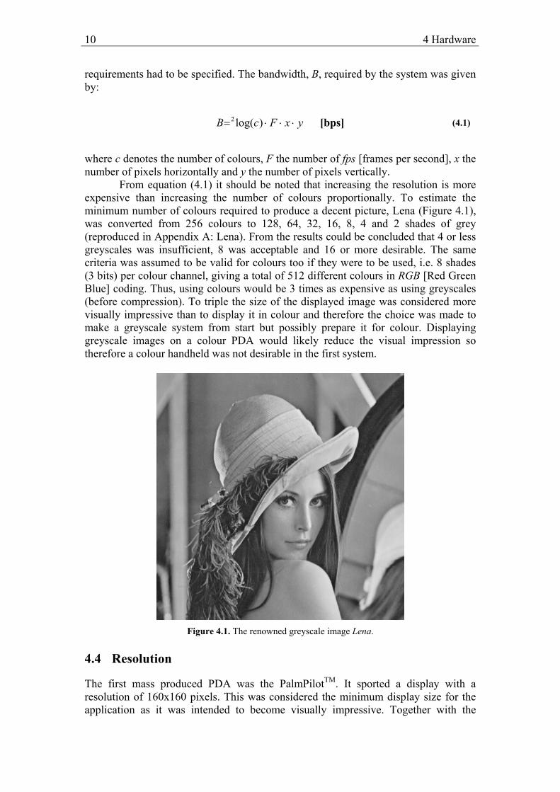
From equation (4.1) it should be noted that increasing the resolution is more expensive than increasing the number of colours proportionally. To estimate the minimum number of colours required to produce a decent picture, Lena (Figure 4.1), was converted from 256 colours to 128, 64, 32, 16, 8, 4 and 2 shades of grey (reproduced in Appendix A: Lena). From the results could be concluded that 4 or less greyscales was insufficient, 8 was acceptable and 16 or more desirable. The same criteria was assumed to be valid for colours too if they were to be used, i.e. 8 shades (3 bits) per colour channel, giving a total of 512 different colours in RGB [Red Green Blue] coding. Thus, using colours would be 3 times as expensive as using greyscales (before compression). To triple the size of the displayed image was considered more visually impressive than to display it in colour and therefore the choice was made to make a greyscale system from start but possibly prepare it for colour. Displaying greyscale images on a colour PDA would likely reduce the visual impression so therefore a colour handheld was not desirable in the first system.
Figure 4.1. The renowned greyscale image Lena.
4.4 Resolution
The first mass produced PDA was the PalmPilotTM. It sported a display with a resolution of 160x160 pixels. This was considered the minimum display size for the application as it was intended to become visually impressive. Together with the
4 Hardware 11
limitations on the data rate, imposed by the serial communication capabilities, and the number of greyscales set to 8, the framerate would in theory reach F fps.
5.1160160)8log(
200,1152 =
⋅⋅=F [fps] (4.2)
To increase the number of colours to the desirable 16 greyscales would lower the framerate to:
125.1160160)16log(
200,1152 =
⋅⋅=F [fps] (4.3)
The 115,200 bps data rate would never be fully reached in practice since the calculations assume data can be transceived at all times. In reality, system resources would be used to sample an image, process and compress it before transmitting it on the ARM side. A portion of the theoretical bandwidth would also be used for header information and similar data, sent with every Bluetooth data packet. The PDA side, upon reception, would also need time to decompress, process and display the image.
It was evident from the framerates in formula (4.2) and (4.3) that increasing the resolution would have a devastating effect on the framerate. Therefore, when choosing PDA, a resolution greater than 160x160 would result in a visually less impressive application since only parts of the display would be filled with relevant content. In order for the handheld device to be able to use its full resolution, the camera side had to capture images at a resolution greater or equal to the PDA’s screen display.
4.5 Choosing PDA
With the findings in the pre-study, the conclusion from section 4.3 and 4.4 together with the objectives specified in section 1.2, both the PDA and the camera could be chosen.
Apart from the guidelines regarding colour and resolution, other considerations had to be taken into account when choosing PDA. The OS [Operating System] running on the handheld device should be easily programmed and well documented. The handheld’s processing power could only be used up to the level of the ARM Thumb processor as noted in section 3.1.3. The handheld’s interface should preferably be compatible with the interface of a Bluetooth module or plug-in. Finally, there should be affordable development tools for the PDA and its OS.
At the time, there were two types of handhelds on the market. High-end, portable computers replicas, and low-end, pocket calendar replacements, PDAs.
The former were fitted with a high resolution display and were usually ARM or StrongARM® powered, with clock frequencies well over the ARM Thumb on the Atmel evaluation board. These high-end machines often run WindowsCE® or PocketPC® as their native OS. WindowsCE, notorious for its stability problems was not an alternative for quick development, neither PocketPC due to the lack of documentation and development tools. Psion’s handhelds where running the EPOC® OS but these machine had too big a resolution to display 160x160 images impressively.
12 4 Hardware
With these ARM or StrongARM powered PDA, the compression limitation would be set by the ARM Thumb processor. The used resolution, however, would have to be increased to better match the PDA’s display. Ultimately, the visual improvements may not be noticeable on either a video or a still image application and much time would have been lost on implementing an excessively powerful compression algorithm.
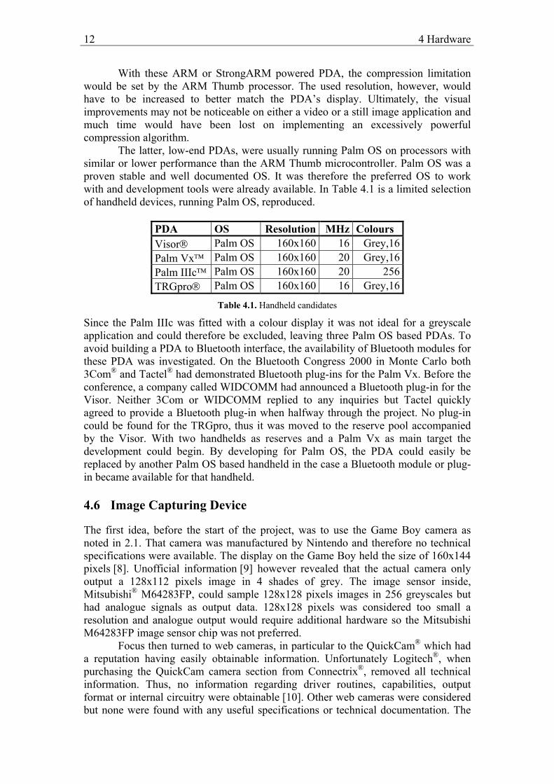
The latter, low-end PDAs, were usually running Palm OS on processors with similar or lower performance than the ARM Thumb microcontroller. Palm OS was a proven stable and well documented OS. It was therefore the preferred OS to work with and development tools were already available. In Table 4.1 is a limited selection of handheld devices, running Palm OS, reproduced.
PDA OS Resolution MHz Colours Visor Palm OS 160x160 16 Grey,16 Palm Vx Palm OS 160x160 20 Grey,16 Palm IIIc Palm OS 160x160 20 256 TRGpro Palm OS 160x160 16 Grey,16
Table 4.1. Handheld candidates
Since the Palm IIIc was fitted with a colour display it was not ideal for a greyscale application and could therefore be excluded, leaving three Palm OS based PDAs. To avoid building a PDA to Bluetooth interface, the availability of Bluetooth modules for these PDA was investigated. On the Bluetooth Congress 2000 in Monte Carlo both 3Com® and Tactel® had demonstrated Bluetooth plug-ins for the Palm Vx. Before the conference, a company called WIDCOMM had announced a Bluetooth plug-in for the Visor. Neither 3Com or WIDCOMM replied to any inquiries but Tactel quickly agreed to provide a Bluetooth plug-in when halfway through the project. No plug-in could be found for the TRGpro, thus it was moved to the reserve pool accompanied by the Visor. With two handhelds as reserves and a Palm Vx as main target the development could begin. By developing for Palm OS, the PDA could easily be replaced by another Palm OS based handheld in the case a Bluetooth module or plug-in became available for that handheld.
4.6 Image Capturing Device
The first idea, before the start of the project, was to use the Game Boy camera as noted in 2.1. That camera was manufactured by Nintendo and therefore no technical specifications were available. The display on the Game Boy held the size of 160x144 pixels [8]. Unofficial information [9] however revealed that the actual camera only output a 128x112 pixels image in 4 shades of grey. The image sensor inside, Mitsubishi® M64283FP, could sample 128x128 pixels images in 256 greyscales but had analogue signals as output data. 128x128 pixels was considered too small a resolution and analogue output would require additional hardware so the Mitsubishi M64283FP image sensor chip was not preferred.
Focus then turned to web cameras, in particular to the QuickCam® which had a reputation having easily obtainable information. Unfortunately Logitech®, when purchasing the QuickCam camera section from Connectrix®, removed all technical information. Thus, no information regarding driver routines, capabilities, output format or internal circuitry were obtainable [10]. Other web cameras were considered but none were found with any useful specifications or technical documentation. The
4 Hardware 13
exception being the Axis® 2100 network camera, which unfortunately was a stand-alone camera and therefore overqualified and too expensive.
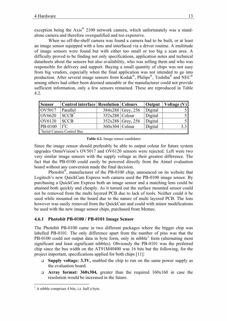
When no off-the-shelf camera was found a camera had to be built, or at least an image sensor equipped with a lens and interfaced via a driver routine. A multitude of image sensors were found but with either too small or too big a scan area. A difficulty proved to be finding not only specifications, application notes and technical datasheets about the sensors but also availability, who was selling them and who was responsible for delivery and support. Buying a small quantity of chips was not easy from big vendors, especially when the final application was not intended to go into production. After several image sensors from Kodak®, Philips®, Toshiba® and NEC® among others had either been deemed unusable or the manufacturer could not provide sufficient information, only a few sensors remained. These are reproduced in Table 4.2.
Sensor Control interface Resolution Colours Output Voltage (V) OV5017 Parallel 384x288 Grey, 256 Digital 5 OV6620 SCCB* 352x288 Colour Digital 5 OV6120 SCCB 352x288 Grey, 256 Digital 5 PB-0100 I2C 360x304 Colour Digital 3.3 *Serial Camera Control Bus
Table 4.2. Image sensor candidates
Since the image sensor should preferably be able to output colour for future system upgrades OmniVision’s OV5017 and OV6120 sensors were rejected. Left were two very similar image sensors with the supply voltage as their greatest difference. The fact that the PB-0100 could easily be powered directly from the Atmel evaluation board without any conversion made the final decision.
Photobit®, manufacturer of the PB-0100 chip, announced on its website that Logitech’s new QuickCam Express web camera used the PB-0100 image sensor. By purchasing a QuickCam Express both an image sensor and a matching lens could be attained both quickly and cheaply. As it turned out the surface mounted sensor could not be removed from the multi layered PCB due to lack of tools. Neither could it be used while mounted on the board due to the nature of multi layered PCB. The lens however was easily removed from the QuickCam and could with minor modifications be used with the new image sensor chips, purchased from Memec.
4.6.1 Photobit PB-0100 / PB-0101 Image Sensor
The Photobit PB-0100 came in two different packages where the bigger chip was labelled PB-0101. The only difference apart from the number of pins was that the PB-0100 could not output data in byte form, only in nibble1 form (alternating most significant and least significant nibbles). Obviously the PB-0101 was the preferred chip since the bus width on the AT91M40400 was 16 bits but the following, for the project important, specifications applied for both chips [11]:
Supply voltage: 3.3V, enabled the chip to run on the same power supply as the evaluation board.
Array format: 360x304, greater than the required 160x160 in case the resolution would be increased in the future.
1 A nibble comprises 4 bits, i.e. half a byte.
14 4 Hardware
Output: digital 8-bit colour (Standard RGB), synchronization signals, facilitated the sampling of the image.
I2C control bus, provided a simple interface for reading from and writing to the chip. Appendix D: I2C describes the I2C standard.
Auto exposure, enabled the system to adopt to different illuminated environments automatically.
Highly programmable/configurable, the sensor could be easily interfaced to the rest of the system.
Clock speed up to 24 MHz, the sensor could not be clocked with the 32.768 MHz masterclock from the evaluation board.
Low power consumption, was desirable in the wireless system.
4.7 Bluetooth to PDA Interface
Tactel unfortunately encountered various problems with their Bluetooth plug-in which postponed the delivery, thus forcing the use of a module from the EBSK instead. The workaround would however be temporary so the simplest solutions were employed when interfacing the Bluetooth module.
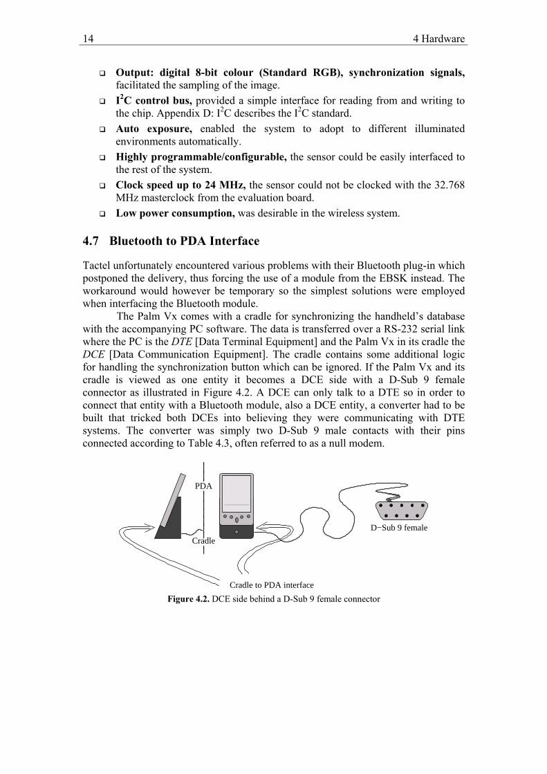
The Palm Vx comes with a cradle for synchronizing the handheld’s database with the accompanying PC software. The data is transferred over a RS-232 serial link where the PC is the DTE [Data Terminal Equipment] and the Palm Vx in its cradle the DCE [Data Communication Equipment]. The cradle contains some additional logic for handling the synchronization button which can be ignored. If the Palm Vx and its cradle is viewed as one entity it becomes a DCE side with a D-Sub 9 female connector as illustrated in Figure 4.2. A DCE can only talk to a DTE so in order to connect that entity with a Bluetooth module, also a DCE entity, a converter had to be built that tricked both DCEs into believing they were communicating with DTE systems. The converter was simply two D-Sub 9 male contacts with their pins connected according to Table 4.3, often referred to as a null modem.
Cradle to PDA interface
D−Sub 9 female
PDA
Cradle
Figure 4.2. DCE side behind a D-Sub 9 female connector
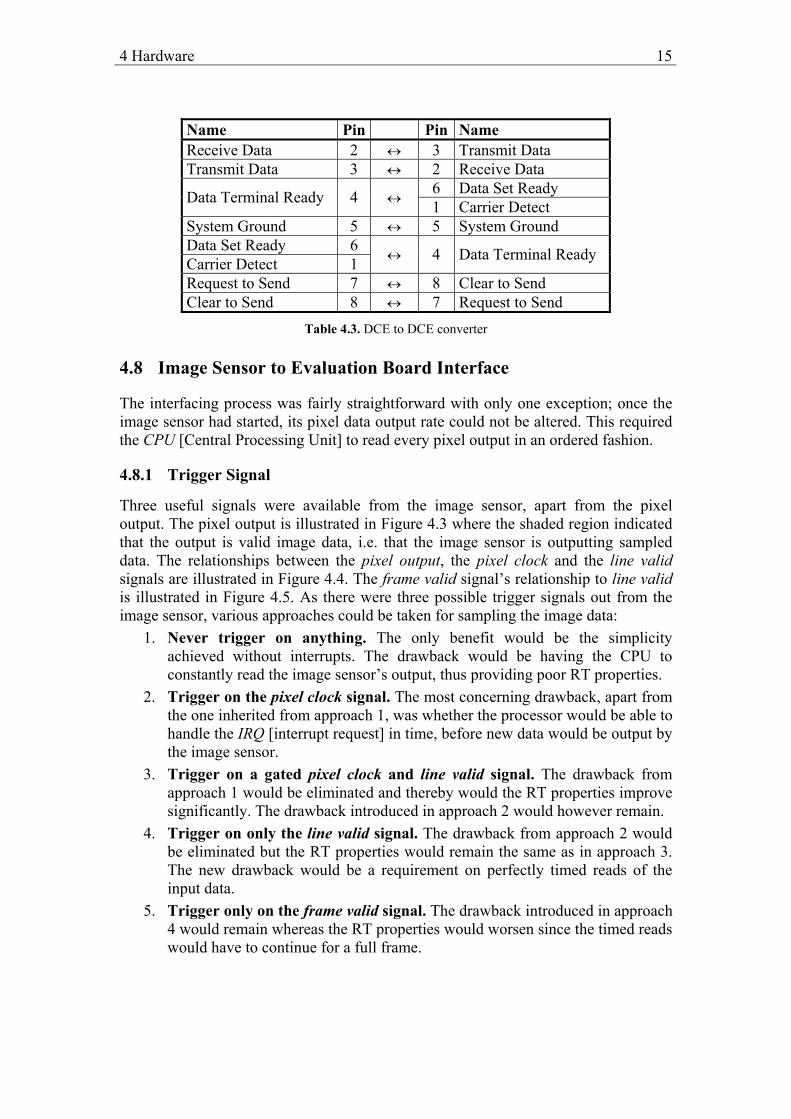
4 Hardware 15
Name Pin Pin Name Receive Data 2 ↔ 3 Transmit Data Transmit Data 3 ↔ 2 Receive Data
6 Data Set Ready Data Terminal Ready 4 ↔ 1 Carrier Detect System Ground 5 ↔ 5 System Ground Data Set Ready 6 Carrier Detect 1 ↔ 4 Data Terminal Ready
Request to Send 7 ↔ 8 Clear to Send Clear to Send 8 ↔ 7 Request to Send
Table 4.3. DCE to DCE converter
4.8 Image Sensor to Evaluation Board Interface
The interfacing process was fairly straightforward with only one exception; once the image sensor had started, its pixel data output rate could not be altered. This required the CPU [Central Processing Unit] to read every pixel output in an ordered fashion.
4.8.1 Trigger Signal
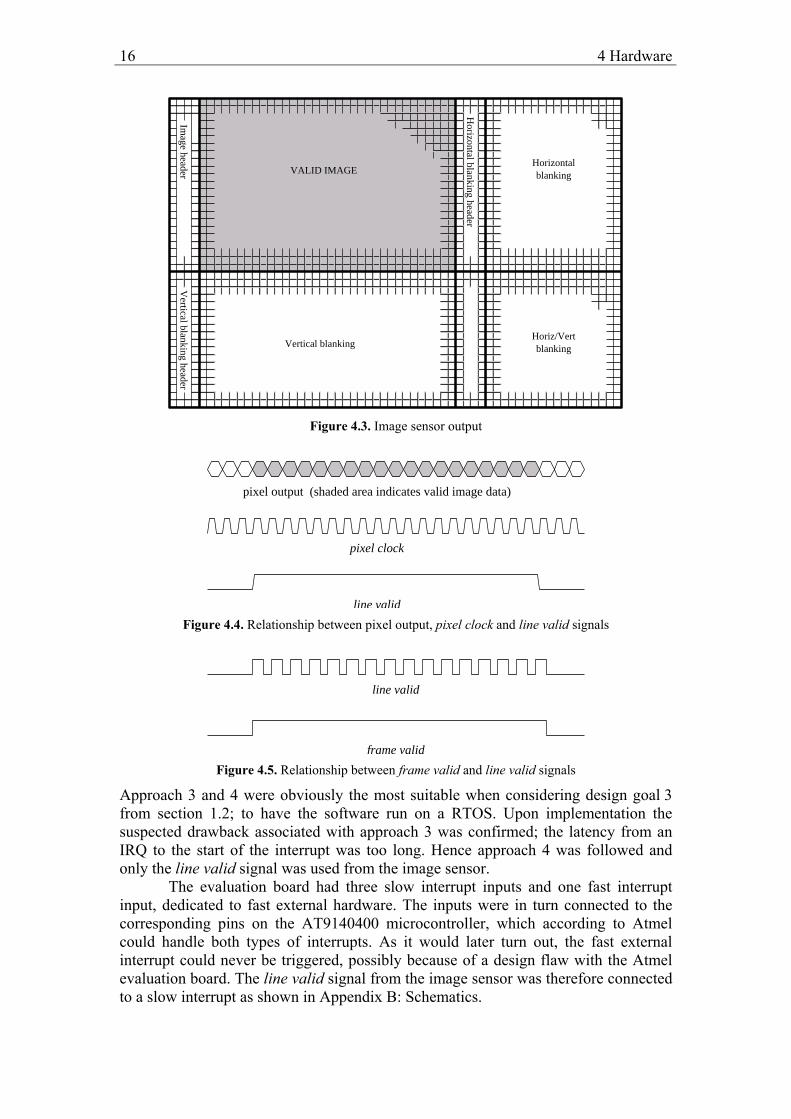
Three useful signals were available from the image sensor, apart from the pixel output. The pixel output is illustrated in Figure 4.3 where the shaded region indicated that the output is valid image data, i.e. that the image sensor is outputting sampled data. The relationships between the pixel output, the pixel clock and the line valid signals are illustrated in Figure 4.4. The frame valid signal’s relationship to line valid is illustrated in Figure 4.5. As there were three possible trigger signals out from the image sensor, various approaches could be taken for sampling the image data:
1. Never trigger on anything. The only benefit would be the simplicity achieved without interrupts. The drawback would be having the CPU to constantly read the image sensor’s output, thus providing poor RT properties.
2. Trigger on the pixel clock signal. The most concerning drawback, apart from the one inherited from approach 1, was whether the processor would be able to handle the IRQ [interrupt request] in time, before new data would be output by the image sensor.
3. Trigger on a gated pixel clock and line valid signal. The drawback from approach 1 would be eliminated and thereby would the RT properties improve significantly. The drawback introduced in approach 2 would however remain.
4. Trigger on only the line valid signal. The drawback from approach 2 would be eliminated but the RT properties would remain the same as in approach 3. The new drawback would be a requirement on perfectly timed reads of the input data.
5. Trigger only on the frame valid signal. The drawback introduced in approach 4 would remain whereas the RT properties would worsen since the timed reads would have to continue for a full frame.
16 4 Hardware
Horizontalblanking
Horiz/Vertblanking
Vertical blanking header
Horizontal blanking header
Image header
Vertical blanking
VALID IMAGE
Figure 4.3. Image sensor output
pixel output (shaded area indicates valid image data)
pixel clock
line valid Figure 4.4. Relationship between pixel output, pixel clock and line valid signals
frame valid
line valid
Figure 4.5. Relationship between frame valid and line valid signals
Approach 3 and 4 were obviously the most suitable when considering design goal 3 from section 1.2; to have the software run on a RTOS. Upon implementation the suspected drawback associated with approach 3 was confirmed; the latency from an IRQ to the start of the interrupt was too long. Hence approach 4 was followed and only the line valid signal was used from the image sensor.
The evaluation board had three slow interrupt inputs and one fast interrupt input, dedicated to fast external hardware. The inputs were in turn connected to the corresponding pins on the AT9140400 microcontroller, which according to Atmel could handle both types of interrupts. As it would later turn out, the fast external interrupt could never be triggered, possibly because of a design flaw with the Atmel evaluation board. The line valid signal from the image sensor was therefore connected to a slow interrupt as shown in Appendix B: Schematics.
4 Hardware 17
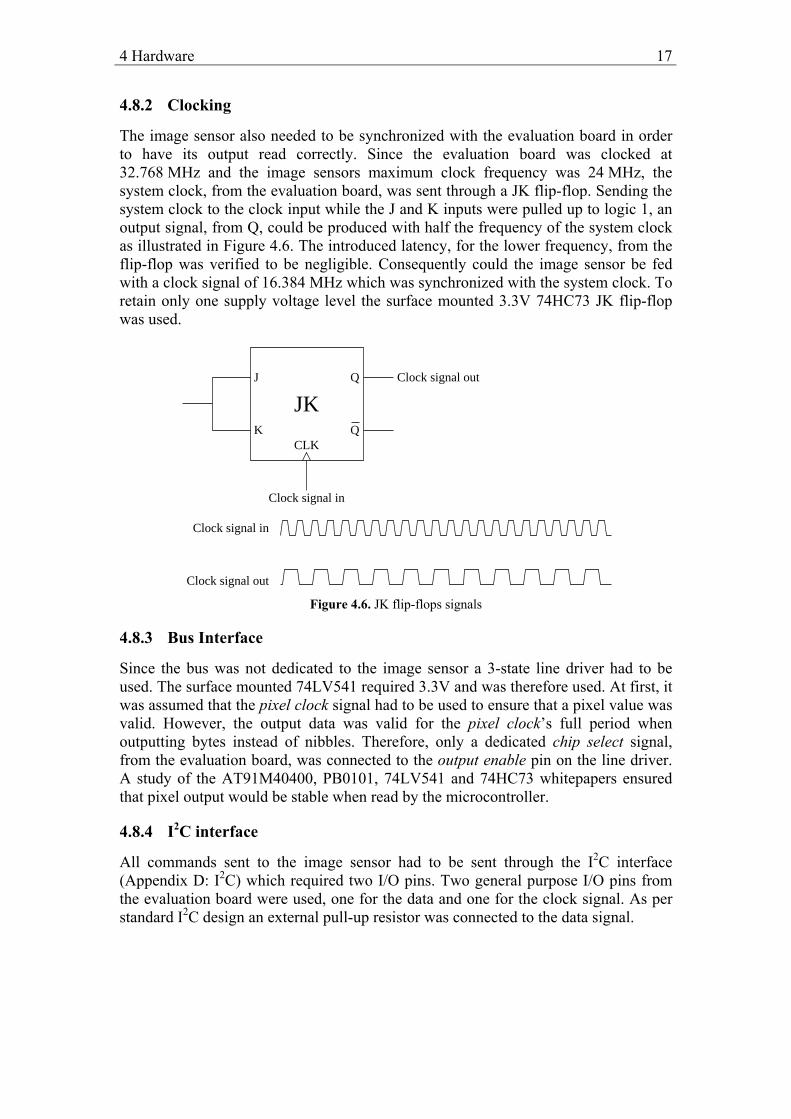
4.8.2 Clocking
The image sensor also needed to be synchronized with the evaluation board in order to have its output read correctly. Since the evaluation board was clocked at 32.768 MHz and the image sensors maximum clock frequency was 24 MHz, the system clock, from the evaluation board, was sent through a JK flip-flop. Sending the system clock to the clock input while the J and K inputs were pulled up to logic 1, an output signal, from Q, could be produced with half the frequency of the system clock as illustrated in Figure 4.6. The introduced latency, for the lower frequency, from the flip-flop was verified to be negligible. Consequently could the image sensor be fed with a clock signal of 16.384 MHz which was synchronized with the system clock. To retain only one supply voltage level the surface mounted 3.3V 74HC73 JK flip-flop was used.
Clock signal in
Clock signal out
CLKQ
QJ
K
1
Clock signal out
Clock signal in
JK
Figure 4.6. JK flip-flops signals
4.8.3 Bus Interface
Since the bus was not dedicated to the image sensor a 3-state line driver had to be used. The surface mounted 74LV541 required 3.3V and was therefore used. At first, it was assumed that the pixel clock signal had to be used to ensure that a pixel value was valid. However, the output data was valid for the pixel clock’s full period when outputting bytes instead of nibbles. Therefore, only a dedicated chip select signal, from the evaluation board, was connected to the output enable pin on the line driver. A study of the AT91M40400, PB0101, 74LV541 and 74HC73 whitepapers ensured that pixel output would be stable when read by the microcontroller.
4.8.4 I2C interface
All commands sent to the image sensor had to be sent through the I2C interface (Appendix D: I2C) which required two I/O pins. Two general purpose I/O pins from the evaluation board were used, one for the data and one for the clock signal. As per standard I2C design an external pull-up resistor was connected to the data signal.
18 4 Hardware
4.8.5 Power Supply
VDD and GND was taken from the evaluation board’s buses (connectors J0 and J1). All the power supply pins had adjacent decoupling capacitors placed with them to guarantee a sufficient current supply.
4.8.6 PB-0101
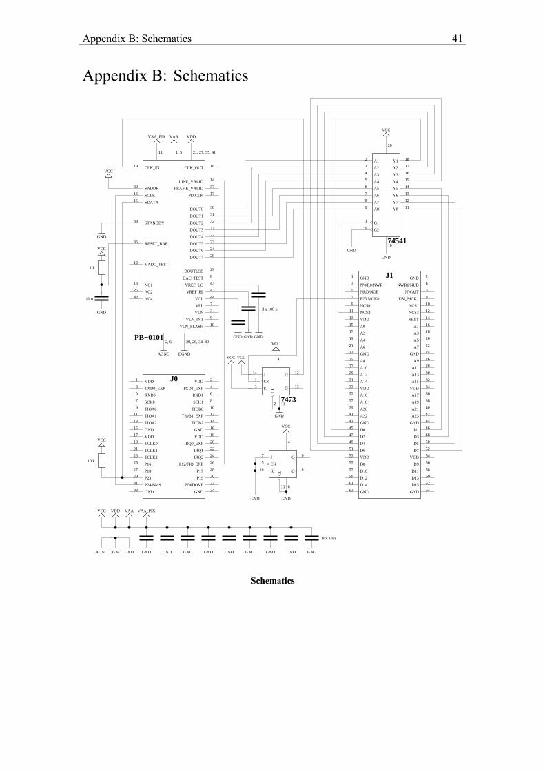
To ensure full functionality from the PB-0101, the design guidelines concerning passive components in [12] were followed. Full schematics of all components and connections are included in Appendix B: Schematics.
5 Software 19
5 Software
The full software on the image sensor side should be able to handle both reading and storing of pixel values, checking the image integrity, processing and compressing the image data before transmitting it. Distinguishing between driver routines and post driver routines is difficult when they are tightly coupled. No attempt of doing so is therefore made here but instead is each piece of software described individually, followed by a description of how the different routines are linked together. At the end of this section is the PDA software, which handles the decompression and displaying of the image data, described.
5.1 Reading the Input
The most suitable model for reading the image sensor output was according to section 4.8.1 approach 4: trigger on the line valid signal and read all following outputs with perfect timing. To achieve perfect timing, each set of read and store operations had to take exactly as long time as the time between the starts of two subsequent outputs and preferably be as short a time as possible for the RT properties. Neither the required precision or the optimisation possibilities could be reached in the C programming language so assembly had to be used.
The ARM Thumb ARM7TDMI microcontroller supports two assembler modes, 16-bit and 32-bit mode. The main advantage with the 16-bit mode is that instructions are faster fetched from memory since the bus width is only 16 bits. However, due to the heritage from the ARM architecture, when entering an interrupt the microcontroller automatically switches to 32-bit mode so the interrupt routine itself has to switch back to 16-bit mode to utilize the speed advantage over the default 32-bit mode. The fastest set of read (load) and store operations in 16 bits ARM assembly takes in total 11 clock cycles and are: ldrb rx,[ry,d5] strb rx,[ry,d5] where rx and ry denotes registers and d5 a five bits signed integer. If an index counter or a pointer were to be increased, the command: add rx,ry,d3 would take the minimum of 2 clock cycles, (the same as the nop [no operation] instruction). d3 denotes a signed three bit integer. The total number of clock cycles to match was given by the image sensor output rate:
42 ⋅⋅= Ir [clock cycles] (5.1)
where I denotes an internal multiplier in the sensor which can be set to 1, 3/2 or 2. The factor 2 comes from the clock frequency being feed through the JK flip-flop and the factor 4 from internal circuitry in the image sensor. The ARM Thumb processor could evidently not read and store all outputs if the internal multiplier was to be set to 1. With the multiplier set to 2, processing power would be wasted waiting 4 extra clock cycles per pixel output in comparison to having the multiplier set to 3/2 and
20 5 Software
increasing the pointer every other sample. With consideration taken to the RT demands the multiplier was set to 3/2, giving an output rate, r, of 1 sample every 12 clock cycles. The critical code for a few sets of read and store with an average execution time of 12 clock cycles per set is reproduced in Table 5.1.
16 bits assembly code: read and store ldrb r0,[r1,0] ; set 1 strb r0,[r2,0] ; set 1, 11 clock cycles used ldrb r0,[r1,0] ; set 2 strb r0,[r2,1] ; set 2 add r2,r2,2 ; set 2 ; 24 used clock cycles ldrb r0,[r1,0] ; set 3 strb r0,[r2,0] ; set 3, 35 clock cycles used ldrb r0,[r1,0] ; set 4 strb r0,[r2,1] ; set 4 add r2,r2,2 ; set 4 ; 48 used clock cycles ...
Table 5.1. Critical code for reading and storing pixel values
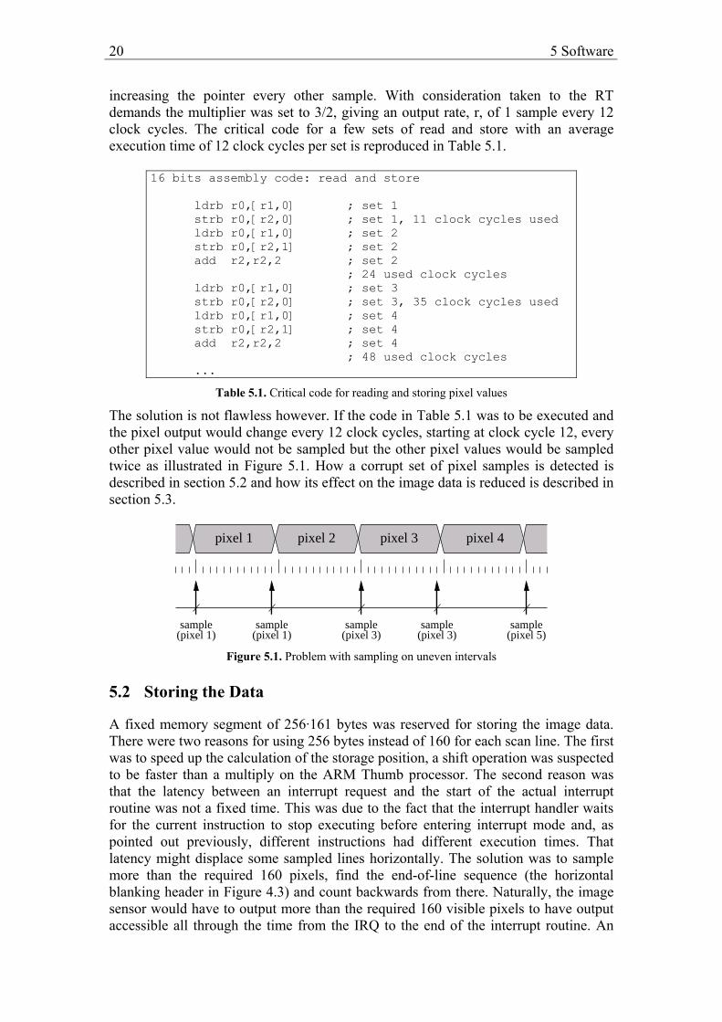
The solution is not flawless however. If the code in Table 5.1 was to be executed and the pixel output would change every 12 clock cycles, starting at clock cycle 12, every other pixel value would not be sampled but the other pixel values would be sampled twice as illustrated in Figure 5.1. How a corrupt set of pixel samples is detected is described in section 5.2 and how its effect on the image data is reduced is described in section 5.3.
sample sample sample sample sample(pixel 1) (pixel 3)(pixel 1) (pixel 3) (pixel 5)
pixel 1 pixel 2 pixel 3 pixel 4
Figure 5.1. Problem with sampling on uneven intervals
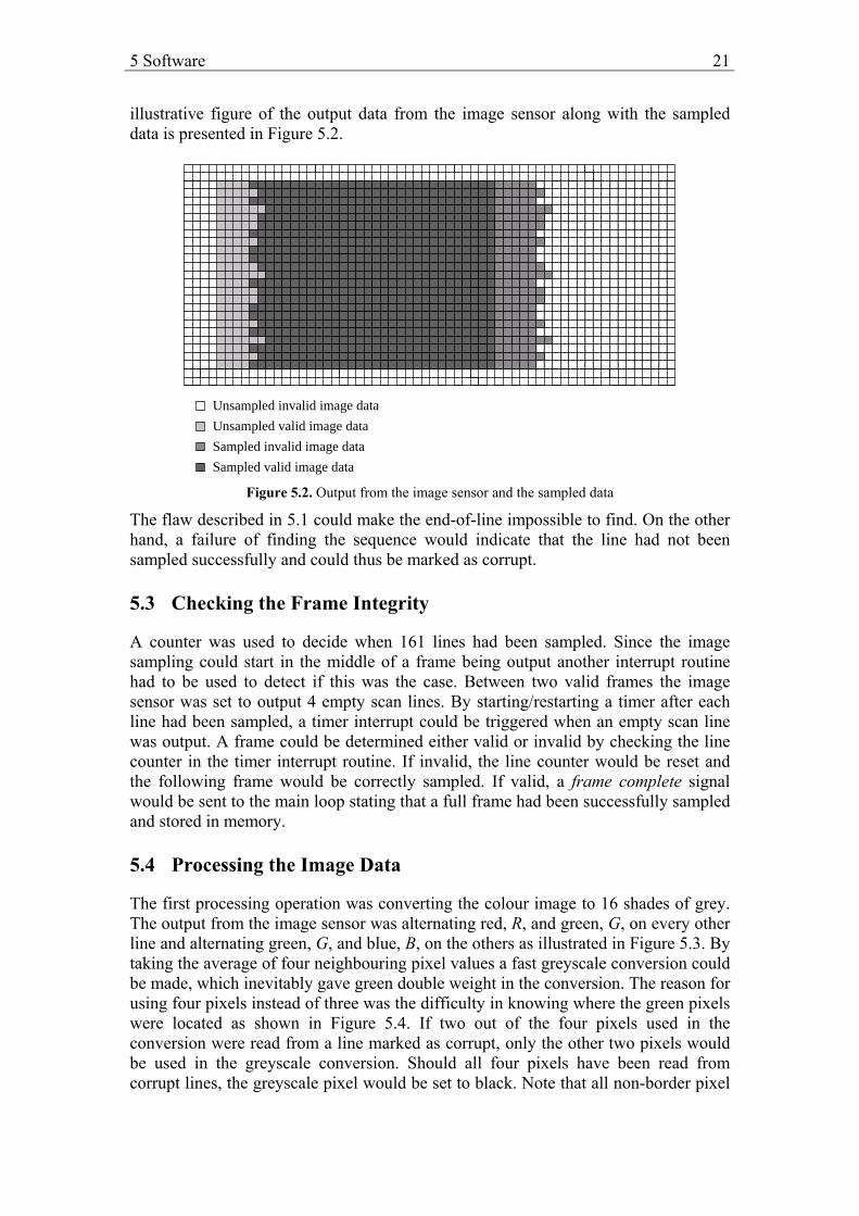
5.2 Storing the Data
A fixed memory segment of 256·161 bytes was reserved for storing the image data. There were two reasons for using 256 bytes instead of 160 for each scan line. The first was to speed up the calculation of the storage position, a shift operation was suspected to be faster than a multiply on the ARM Thumb processor. The second reason was that the latency between an interrupt request and the start of the actual interrupt routine was not a fixed time. This was due to the fact that the interrupt handler waits for the current instruction to stop executing before entering interrupt mode and, as pointed out previously, different instructions had different execution times. That latency might displace some sampled lines horizontally. The solution was to sample more than the required 160 pixels, find the end-of-line sequence (the horizontal blanking header in Figure 4.3) and count backwards from there. Naturally, the image sensor would have to output more than the required 160 visible pixels to have output accessible all through the time from the IRQ to the end of the interrupt routine. An
5 Software 21
illustrative figure of the output data from the image sensor along with the sampled data is presented in Figure 5.2.
Unsampled valid image data
Sampled invalid image data
Sampled valid image data
Unsampled invalid image data
Figure 5.2. Output from the image sensor and the sampled data
The flaw described in 5.1 could make the end-of-line impossible to find. On the other hand, a failure of finding the sequence would indicate that the line had not been sampled successfully and could thus be marked as corrupt.
5.3 Checking the Frame Integrity
A counter was used to decide when 161 lines had been sampled. Since the image sampling could start in the middle of a frame being output another interrupt routine had to be used to detect if this was the case. Between two valid frames the image sensor was set to output 4 empty scan lines. By starting/restarting a timer after each line had been sampled, a timer interrupt could be triggered when an empty scan line was output. A frame could be determined either valid or invalid by checking the line counter in the timer interrupt routine. If invalid, the line counter would be reset and the following frame would be correctly sampled. If valid, a frame complete signal would be sent to the main loop stating that a full frame had been successfully sampled and stored in memory.
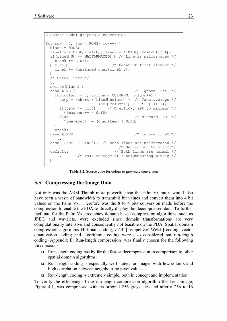
5.4 Processing the Image Data
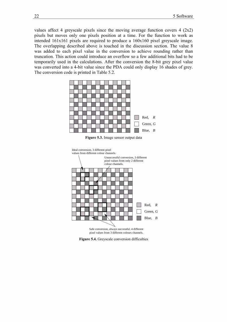
The first processing operation was converting the colour image to 16 shades of grey. The output from the image sensor was alternating red, R, and green, G, on every other line and alternating green, G, and blue, B, on the others as illustrated in Figure 5.3. By taking the average of four neighbouring pixel values a fast greyscale conversion could be made, which inevitably gave green double weight in the conversion. The reason for using four pixels instead of three was the difficulty in knowing where the green pixels were located as shown in Figure 5.4. If two out of the four pixels used in the conversion were read from a line marked as corrupt, only the other two pixels would be used in the greyscale conversion. Should all four pixels have been read from corrupt lines, the greyscale pixel would be set to black. Note that all non-border pixel
22 5 Software
values affect 4 greyscale pixels since the moving average function covers 4 (2x2) pixels but moves only one pixels position at a time. For the function to work as intended 161x161 pixels are required to produce a 160x160 pixel greyscale image. The overlapping described above is touched in the discussion section. The value 8 was added to each pixel value in the conversion to achieve rounding rather than truncation. This action could introduce an overflow so a few additional bits had to be temporarily used in the calculations. After the conversion the 8-bit grey pixel value was converted into a 4-bit value since the PDA could only display 16 shades of grey. The conversion code is printed in Table 5.2.
Red,
Green,
Blue,
G
B
R
Figure 5.3. Image sensor output data
R
G
B
Safe conversion, always successful. 4 different
Ideal conversion, 3 different pixelvalues from different colour channels.
Unsuccessful conversion, 3 differentpixel values from only 2 differentcolour channels.
pixel values from 3 different colours channels.
Red,
Green,
Blue,
Figure 5.4. Greyscale conversion difficulties
5 Software 23
C source code: greyscale conversion for(row = 0; row < ROWS; row++) { black = NONE; line1 = &IMAGE[row<<8]; line2 = &IMAGE[(row<<8)+256]; if(line1[0] == MALFORMATED) { /* Line is malformated */ black += LINE1; } else { /* Point at first element */ line1 += (unsigned char)line1[0]; } /* Check line2 */ ... switch(black) { case LINE1: /* Ignore line1 */ for(column = 0; column < COLUMNS; column++) { temp = (short)((line2[column] + /* Take average */ line2[column+1] + 2 * 8) << 1); if(temp >= 0xff) /* Overflow, set to maximum */ *imageout++ = 0xf0; else /* discard LSB */ *imageout++ = (char)temp & 0xf0; } break; case LINE2: /* Ignore line2 */ ... case (LINE1 + LINE2): /* Both lines are malformated */ ... /* Set output to black */ default: /* Both lines are normal */ ... /* Take average of 4 neighbouring pixels */ } }
Table 5.2. Source code for colour to greyscale conversion
5.5 Compressing the Image Data
Not only was the ARM Thumb more powerful than the Palm Vx but it would also have been a waste of bandwidth to transmit 8 bit values and convert them into 4 bit values on the Palm Vx. Therefore was the 8 to 4 bits conversion made before the compression to enable the PDA to directly display the decompressed data. To further facilitate for the Palm Vx, frequency domain based compression algorithms, such as JPEG and wavelets, were excluded since domain transformations are very computationally intensive and consequently not feasible on the PDA. Spatial domain compression algorithms Huffman coding, LZW [Lempel-Ziv-Welsh] coding, vector quantization coding and algorithmic coding were also considered but run-length coding (Appendix E: Run-length compression) was finally chosen for the following three reasons:
Run-length coding has by far the fastest decompression in comparison to other spatial domain algorithms.
Run-length coding is especially well suited for images with few colours and high correlation between neighbouring pixel values.
Run-length coding is extremely simple, both in concept and implementation. To verify the efficiency of the run-length compression algorithm the Lena image, Figure 4.1, was compressed with its original 256 greyscales and after a 256 to 16
24 5 Software
greyscales conversion. The compression for the former became 1.1:1 and for the latter 2.9:1. It was estimated that if the latter could be compressed with such a ratio should simpler scenes be possible to compress with ratios of more than 4:1.
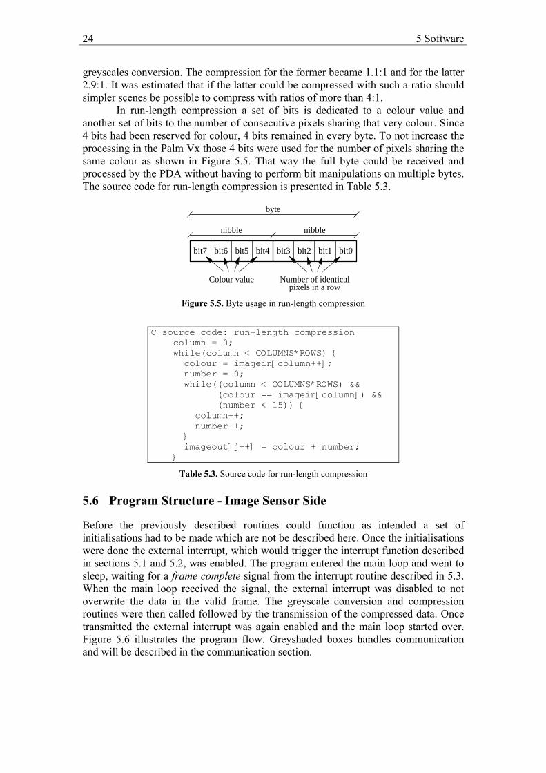
In run-length compression a set of bits is dedicated to a colour value and another set of bits to the number of consecutive pixels sharing that very colour. Since 4 bits had been reserved for colour, 4 bits remained in every byte. To not increase the processing in the Palm Vx those 4 bits were used for the number of pixels sharing the same colour as shown in Figure 5.5. That way the full byte could be received and processed by the PDA without having to perform bit manipulations on multiple bytes. The source code for run-length compression is presented in Table 5.3.
Colour value Number of identical
nibble nibble
byte
pixels in a row
bit7 bit6 bit5 bit4 bit3 bit2 bit1 bit0
Figure 5.5. Byte usage in run-length compression
C source code: run-length compression column = 0; while(column < COLUMNS*ROWS) { colour = imagein[column++]; number = 0; while((column < COLUMNS*ROWS) && (colour == imagein[column]) && (number < 15)) { column++; number++; } imageout[j++] = colour + number; }
Table 5.3. Source code for run-length compression
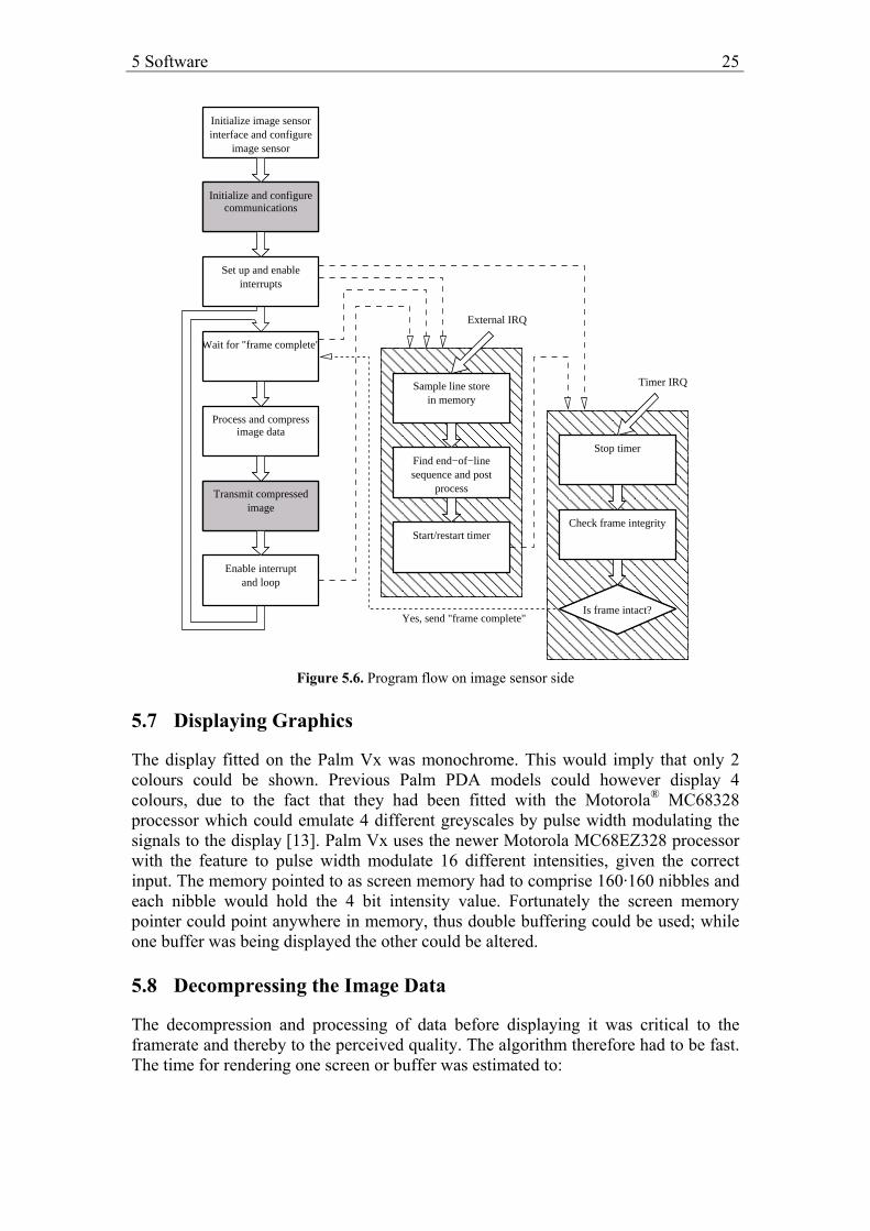
5.6 Program Structure - Image Sensor Side
Before the previously described routines could function as intended a set of initialisations had to be made which are not be described here. Once the initialisations were done the external interrupt, which would trigger the interrupt function described in sections 5.1 and 5.2, was enabled. The program entered the main loop and went to sleep, waiting for a frame complete signal from the interrupt routine described in 5.3. When the main loop received the signal, the external interrupt was disabled to not overwrite the data in the valid frame. The greyscale conversion and compression routines were then called followed by the transmission of the compressed data. Once transmitted the external interrupt was again enabled and the main loop started over. Figure 5.6 illustrates the program flow. Greyshaded boxes handles communication and will be described in the communication section.
5 Software 25
������������������������������������������������������������������������������������������������
������������������������������������������������������������������������������������������������
������������������������������������������������������������������������������������������������
������������������������������������������������������������������������������������������������
Initialize image sensorinterface and configure
image sensor
Initialize and configurecommunications
Set up and enableinterrupts
Process and compressimage data
Transmit compressedimage
in memorySample line store
Find end−of−linesequence and post
process
Start/restart timer
Enable interruptand loop
Stop timer
Check frame integrity
Timer IRQ
Is frame intact?
External IRQ
Yes, send "frame complete"
Wait for "frame complete"
Figure 5.6. Program flow on image sensor side
5.7 Displaying Graphics
The display fitted on the Palm Vx was monochrome. This would imply that only 2 colours could be shown. Previous Palm PDA models could however display 4 colours, due to the fact that they had been fitted with the Motorola® MC68328 processor which could emulate 4 different greyscales by pulse width modulating the signals to the display [13]. Palm Vx uses the newer Motorola MC68EZ328 processor with the feature to pulse width modulate 16 different intensities, given the correct input. The memory pointed to as screen memory had to comprise 160·160 nibbles and each nibble would hold the 4 bit intensity value. Fortunately the screen memory pointer could point anywhere in memory, thus double buffering could be used; while one buffer was being displayed the other could be altered.
5.8 Decompressing the Image Data
The decompression and processing of data before displaying it was critical to the framerate and thereby to the perceived quality. The algorithm therefore had to be fast. The time for rendering one screen or buffer was estimated to:
26 5 Software
610160160
⋅⋅=
EfAt [s] (5.2)
where A denotes the average number of operations required to decode and process one pixel and fE denotes the performance of the processor in MOPS [Millions of Operations Per Second]. According to the specifications [14] the MC68EZ328 reached 3.1 MOPS when running on 20 MHz. Here are only the results for run-length decompression presented but the choice of compression algorithm is explained in Appendix C: Importance of compression algorithm. If the source code in Table 5.4 is rewritten in 68k assembler, it can be calculated that if image data have been compressed with a ration of 4:1, an average, A, of 8 simple assembler instructions are needed per pixel to decompress and render it on screen. The time taken to render a full screen or buffer therefore became:
066.0101.3
8160160 6 ≈⋅
⋅=t [s] (5.3)
Finally, it should be noted that it is possible to boost Palm Vx’s clock frequency to 32 MHz in a software hack but this is not taken into consideration here.
5 Software 27
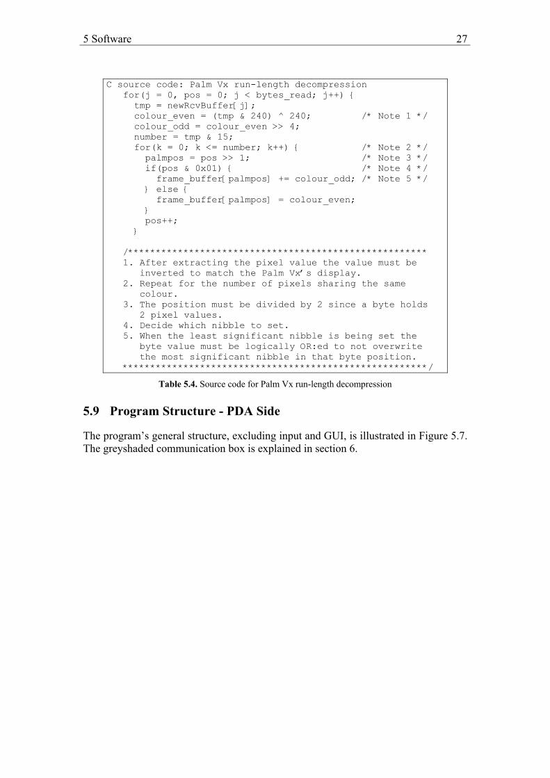
C source code: Palm Vx run-length decompression for(j = 0, pos = 0; j < bytes_read; j++) { tmp = newRcvBuffer[j]; colour_even = (tmp & 240) ^ 240; /* Note 1 */ colour_odd = colour_even >> 4; number = tmp & 15; for(k = 0; k <= number; k++) { /* Note 2 */ palmpos = pos >> 1; /* Note 3 */ if(pos & 0x01) { /* Note 4 */ frame_buffer[palmpos] += colour_odd; /* Note 5 */ } else { frame_buffer[palmpos] = colour_even; } pos++; } /****************************************************** 1. After extracting the pixel value the value must be inverted to match the Palm Vx’s display. 2. Repeat for the number of pixels sharing the same colour. 3. The position must be divided by 2 since a byte holds 2 pixel values. 4. Decide which nibble to set. 5. When the least significant nibble is being set the byte value must be logically OR:ed to not overwrite the most significant nibble in that byte position. *******************************************************/
Table 5.4. Source code for Palm Vx run-length decompression
5.9 Program Structure - PDA Side
The program’s general structure, excluding input and GUI, is illustrated in Figure 5.7. The greyshaded communication box is explained in section 6.
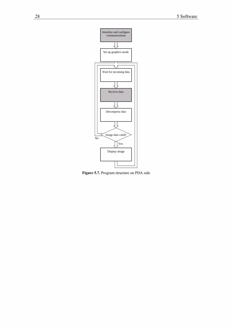
28 5 Software
Image data valid?No
Yes
Set up graphics mode
Initialize and configurecommunications
Wait for incoming data
Receive data
Decompress data
Display image
Figure 5.7. Program structure on PDA side
6 Communication 29
6 Communication
According to the specifications in section 1.1, the communication was supposed to be taking place over a Bluetooth connection. However, as noted in the background section, the evaluation board to Bluetooth interface was to be provided by another master thesis project. Since that project did not deliver on time a temporary solution was employed to test, verify and evaluate the rest of the system. At the time of the implementation it also became evident that the master thesis project which was supposed to provide a RTOS and a TCP stack, also described in the background section, had failed and neither would be provided.
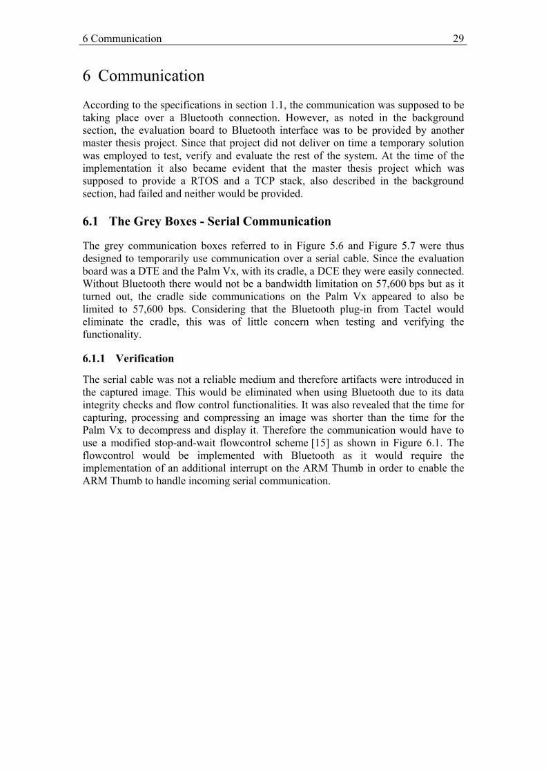
6.1 The Grey Boxes - Serial Communication
The grey communication boxes referred to in Figure 5.6 and Figure 5.7 were thus designed to temporarily use communication over a serial cable. Since the evaluation board was a DTE and the Palm Vx, with its cradle, a DCE they were easily connected. Without Bluetooth there would not be a bandwidth limitation on 57,600 bps but as it turned out, the cradle side communications on the Palm Vx appeared to also be limited to 57,600 bps. Considering that the Bluetooth plug-in from Tactel would eliminate the cradle, this was of little concern when testing and verifying the functionality.
6.1.1 Verification
The serial cable was not a reliable medium and therefore artifacts were introduced in the captured image. This would be eliminated when using Bluetooth due to its data integrity checks and flow control functionalities. It was also revealed that the time for capturing, processing and compressing an image was shorter than the time for the Palm Vx to decompress and display it. Therefore the communication would have to use a modified stop-and-wait flowcontrol scheme [15] as shown in Figure 6.1. The flowcontrol would be implemented with Bluetooth as it would require the implementation of an additional interrupt on the ARM Thumb in order to enable the ARM Thumb to handle incoming serial communication.
30 6 Communication
Lost packet
Image data
Request image data
Request image data
Request image data
Image data
Timeout
Acknowledge,Start timer
Acknowledge,Start timer
Start,Start timer
Stop timer
Send image data
Send image data
Time Time
Image capturing side PDA side
Figure 6.1. Modified stop-and-wait protocol
6.2 The Grey Boxes - Bluetooth Communication
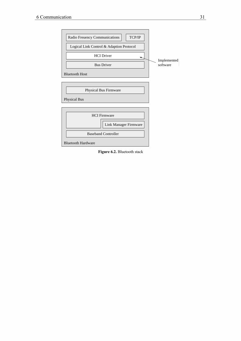
When the Bluetooth software eventually ran on the ARM Thumb the same software was ported to the Palm Vx up to the HCI [Host Controller Interface] layer. Figure 6.2 shows the layers of the Bluetooth stack of which the software layers had been implemented on the ARM Thumb in project 1, described in the background section. The reason for not porting more layers was that it was time consuming and served no purpose when TCP was not to be used anymore. The difference in the grey boxes was that data was sent to Bluetooth modules and therefore had to be encapsulated in packets first. Another difference was that during the initialisations a connection also had to be established or the Bluetooth units would have nowhere to send its data. The results of the Bluetooth implementation is discussed in section 7.2.
6 Communication 31
Physical Bus Firmware
Link Manager Firmware
HCI Firmware
Baseband Controller
Bluetooth Host
Physical Bus
Bluetooth Hardware
Radio Freuency Communications TCP/IP
Bus Driver softwareImplemented
HCI Driver
Logical Link Control & Adaption Protocol
Figure 6.2. Bluetooth stack

32 6 Communication
7 Results 33
7 Results
This results section is divided into two different parts. The first presents the results achieved with the serial link described in 6.1 and the second is concerned with the Bluetooth implementation described in 6.2.
7.1 Serial Link Results
As previously noted in 6.1, the link only reached transmission rates of 57,600 bps and no flowcontrol mechanisms were implemented. Therefore the framerate could not be accurately measured. However, a fair estimate could be calculated. The time taken for decompressing and rendering a full screen is given by equation (5.3). The time required to transfer a full frame is, from Appendix C:, given by:
B
Rt XXTRANS
8160160,
⋅⋅= [s] (7.1)
where the compression ratio, RX, is set to 4 (4:1) and the bandwidth, B, to 57,600 bps. The total time for transferring and decompressing one frame thus becomes:
1066.0889.0 ≈+≈+= DECOMPTRANSTOT ttt [s] (7.2)
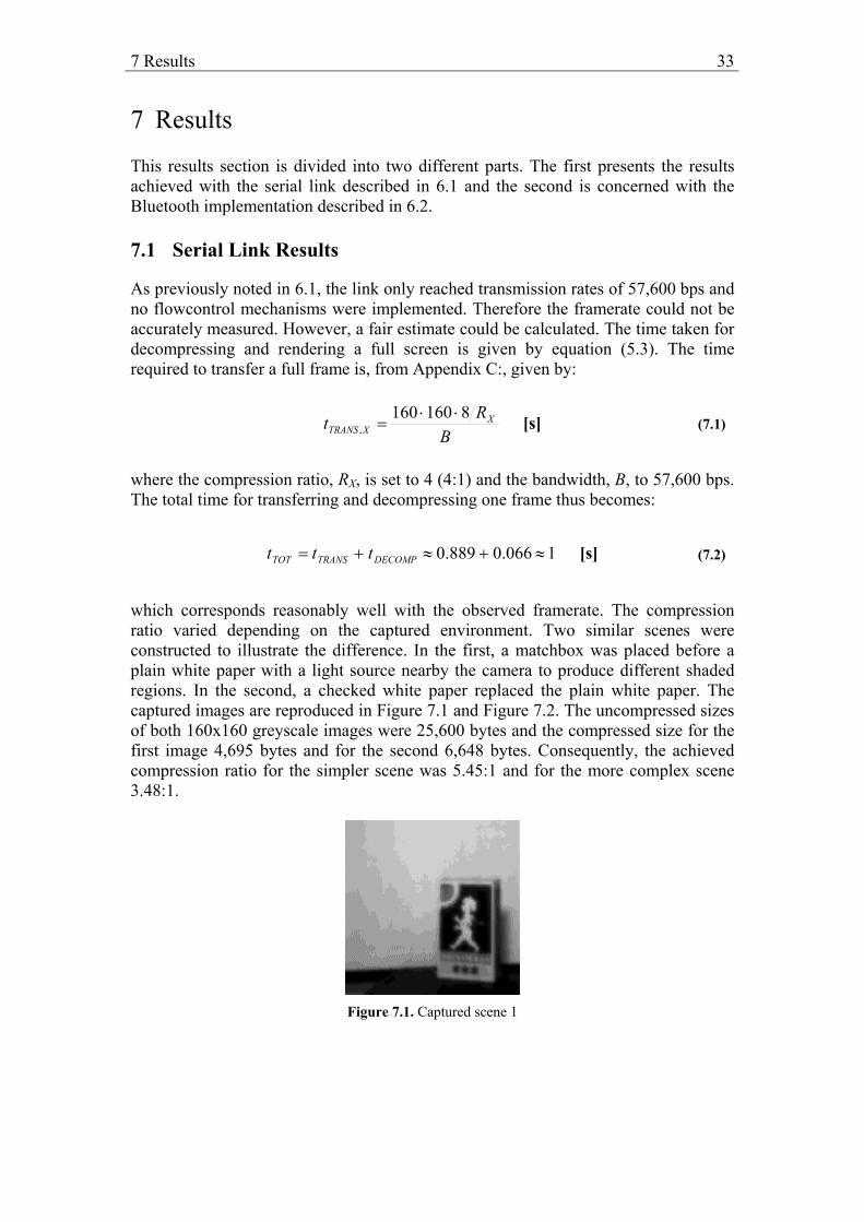
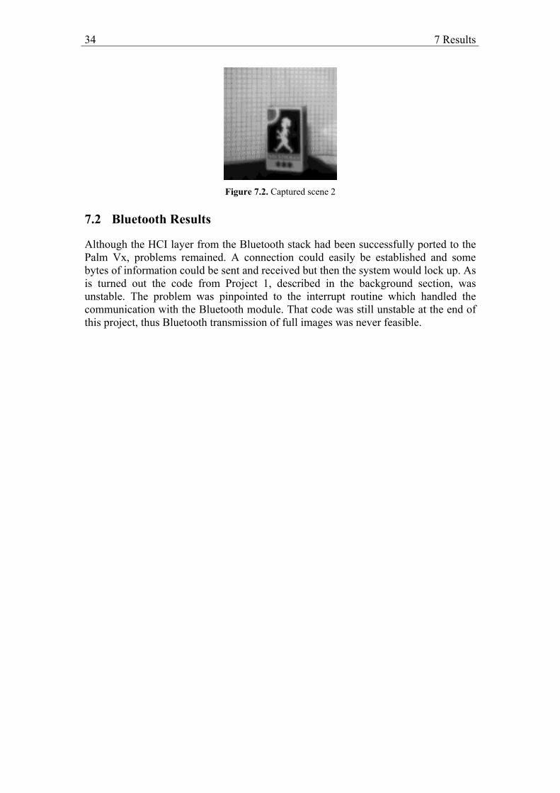
which corresponds reasonably well with the observed framerate. The compression ratio varied depending on the captured environment. Two similar scenes were constructed to illustrate the difference. In the first, a matchbox was placed before a plain white paper with a light source nearby the camera to produce different shaded regions. In the second, a checked white paper replaced the plain white paper. The captured images are reproduced in Figure 7.1 and Figure 7.2. The uncompressed sizes of both 160x160 greyscale images were 25,600 bytes and the compressed size for the first image 4,695 bytes and for the second 6,648 bytes. Consequently, the achieved compression ratio for the simpler scene was 5.45:1 and for the more complex scene 3.48:1.
Figure 7.1. Captured scene 1
34 7 Results
Figure 7.2. Captured scene 2
7.2 Bluetooth Results
Although the HCI layer from the Bluetooth stack had been successfully ported to the Palm Vx, problems remained. A connection could easily be established and some bytes of information could be sent and received but then the system would lock up. As is turned out the code from Project 1, described in the background section, was unstable. The problem was pinpointed to the interrupt routine which handled the communication with the Bluetooth module. That code was still unstable at the end of this project, thus Bluetooth transmission of full images was never feasible.
8 Discussion 35
8 Discussion
8.1 The Project in General
If the project had not been limited to a small budget or if development systems and tools, especially for hardware, had been available, much time could have been saved. By intending to merge the three different projects without a feasible time frame or a more thorough plan severe stalls were invited. The concept could have worked better and would likely have introduced less delays if more time had been invested before and during the projects for planning, guidance and follow ups.
8.2 Tools
Programming interrupt on a new processor without having the ability to emulate, stop or step code is difficult. The development tools used for the Atmel evaluation board were unstable, with time-limited evaluation versions which did not support emulation of interrupts. The interface between the PC and the evaluation board was unstable and interrupt driven which made it impossible to debug interrupt driven software on the evaluation board. As noted in section 4.1 the microcontroller on the evaluation board was fitted with ICE to facilitate debugging of advanced software such as interrupts. If the hardware been available to make use of this system, development times could have been cut by several weeks. Also, if a working development environment had been used, parts of the software could have been emulated before being tested in the system, which would also have decreased development times.
8.3 PDA
Although the Palm Vx fulfilled its purpose a few other considerations should have been taken into account. The 3.1 MOPS were nowhere near the capacity of the ARM Thumb microcontroller so in retrospect a more powerful PDA could have boosted the throughput, especially when the bandwidth never reached higher than 57,600 bps (likely due to the PDA’s cradle). On the other hand, implementing another algorithm could have taken more time from the other parts of the project. An unused option is to increase the clock frequency of the Palm Vx from 20 MHz to 32 MHz in a software hack as noted in section 5.8 and thereby improving the performance.
8.4 Bluetooth
If the postponements of all Bluetooth chips, modules and plug-ins had been foreseen this project would not have ported parts of the Bluetooth stack to Palm OS and maximizing performance for some other form of transmission would have been prioritised.
8.5 Compression Algorithm
The choice of algorithm may not be optimal for the final system. If more time been available, other algorithms could have been implemented and compared to the run-length algorithm. It should be noted that the estimated 4:1 compression ration for run-length encoding was pessimistic and the estimate of 3.25 instructions for
36 8 Discussion
decompressing a pixel therefore also pessimistic. Intended scenes for the camera were simpler than the scene in Figure 7.1 so a more accurate average compression ration was measured to roughly 6:1. The assembler instructions used in run-length decompression were simple and fast instructions whereas the MOPS measurement includes slow operations such as division and multiplication. For this reason was also the 3.1 MOPS measurement pessimistic to use.
8.6 Image sensor
As can be seen in Figure 7.1 and Figure 7.2 not much detail is preserved. This is due to the colour to grey conversion, where a moving average algorithm is used. In retrospect, the image sensor should have output more than 320x320 pixels to enable a mapping from 4 unique pixels to 1 grey pixel, without any overlapping.
8.7 Conclusions
The project met two out of the three objectives stated in section 1.2. The reason it did not meet all the objectives was its dependency on another master thesis, which was not completed on time. Better resource allocation and defined time frames for all three project could have improved the end result. The three projects never merged as intended, which resulted in certain functionality were needlessly implemented. In conclusion, the inter-project dependency created requirements that led to a less than optimal solution.
References 37
References
[1] Bluetooth SIG, Specification of the Bluetooth System: Core, Version 1.0, 1999.
[2] Atmel Corporation, AT91 Third Party Development Tools, Document number 1307A-7/99/12M, 1999.
[3] James D. Murray, William Vanryper, Encyclopedia of Graphics File Formats, O’Reilly & Associates, 2nd edition, June 1996. ASIN: 1565921612.
[4] V. Bhaskaran and K. Konstantinides, Image and Video Compression Standards, Kluwer Academic Publishers, 2nd edition, 1997. ISBN 0-7923-9952-8.
[5] Advanced RISC Machined Ltd (ARM), ARM7TDMI Datasheet, Document number ARM DDI 0029E, August 1995.
[6] Atmel corporation, AT91M40400, Revision 0768C-10/99. [7] W. Stallings, Computer Organization and Architecture, Prentice Hall, 5th
edition, 2000. ISBN 0-13-081294-3. [8] Pan of ATX, Everything you always wanted to know about GAMEBOY,
http://www.programmersheaven.com/zone8/cat38/887.htm [9] Liquid Horizon, Artificial Retina FAQ,
http://www.lh.co.nz/resources/ar/faq.htm [10] Hanno Mueller, Patrick Reynolds, The Connectrix Quickcam Technical FAQ
(Proposal), http://www.cs.duke.edu/~reynolds/quickcam/ [11] Photobit Corporation, PB-0100/PB-0101 Product Specification, Version 3.0,
March 2000. [12] Sten Benda, Störningsfri Elektronik - Konstruktion och Användning,
Studentliteratur, 2nd edition, 1990. ISBN 91-44-28811-5. [13] Edward Keves, Hacking the Pilot: Bypassing the Palm OS. PDA Developers,
pages 900-912, Creative Digital Publishing Inc, Nov/Dec 1996. [14] Motorola Inc, Product Brief MC68EZ328 Dragonball-EZ, MC68EZ328/H,
Rev 1.1 [15] William Stallings, Data & Computer Communications, Prentice Hall, 6th
edition, November 2, 1999, ISBN: 0130843709.

38 References
Appendix A: Lena 39
Appendix A: Lena
Lena 256 greyscales
Lena 128 greyscales
Lena 64 greyscales
Lena 32 greyscales
Lena 16 greyscales
Lena 8 greyscales
Lena 4 greyscales
Lena 2 greyscales

40 Appendix A: Lena
Appendix B: Schematics 41
Appendix B: Schematics
19
12
36
38
15
16
39
25
13
42
18
10
9
3
7
44
4
43
8
29
28
24
23
22
33
32
31
30
17
37
14
CLK_IN
STANDBY
RESET_BAR
SDATA
SCLK
SADDR
VADC_TEST
NC4
NC2
NC1
2
19
1
9
8
7
5
4
3
6
Y1A1
Y8
Y7
Y6
Y5
Y4
Y3
Y2
G2
G1
A8
A7
A6
A5
A4
A3
A2
18
11
12
13
14
15
16
17
10
20
GND
VCC
74541
1
33
31
29
27
25
23
21
19
17
15
13
11
9
7
5
3
2
32
30
28
26
24
22
20
18
16
14
12
10
8
6
4
34GND
VDD
RXD1
SCK1
TIOB0
TIOB2
GND
VDD
IRQ1
IRQ2
P17
P19
NWDOVF
TCD1_EXP
TIOB1_EXP
IRQ0_EXP
P12/FIQ_EXP
VDD
RXD0
SCK0
TIOA0
TIOA1
TIOA2
GND
VDD
TCLK0
TCLK1
TCLK2
P16
P18
P23
P24/BMS
GND
TXD0_EXP
J0
GND
J
K
CL Q
Q
CK
J
K
CL Q
Q
CK
1
3
5
7
9
11
13
15
17
19
21
23
25
27
29
31
33
35
37
39
41
43
47
45
49
51
53
55
57
59
61
63 64
62
60
58
56
54
52
50
48
46
44
42
40
38
36
34
32
30
28
26
24
22
20
18
16
14
12
10
8
6
4
2
GND
D14
D12
D10
D8
VDD
D6
D4
D2
D0
GND
A22
A20
A18
A16
VDD
A14
A12
A10
A8
GND
A6
A4
A2
A0
VDD
NCS2
NCS0
P25/MCK0
GND
NWR0/NWR
NRD/NOE
EBI_MCK1
NWAIT
NWR1/NUB
GND
D15
D13
D11
D9
VDD
D7
D5
D3
D1
GND
A23
A21
A19
A17
VDD
A15
A13
A11
A9
GND
A7
A5
A3
A1
NRST
NCS3
NCS1
GNDJ1
VCC
CLK_OUT
VLN_FLASH
VLN_INT
VLN
VPL
VCL
VREF_HI
VREF_LO
DAC_TEST
DOUTLSB
DOUT7
DOUT6
DOUT5
DOUT4
DOUT3
DOUT2
DOUT1
DOUT0
PIXCLK
LINE_VALID
FRAME_VALID
VCC
GND
VCC
GND
AGND DGND
2, 6 20, 26, 34, 40
VAA_PIX VDD
11
VAA
1, 5 21, 27, 35, 41
1 k
10 k
PB−0101
GND
7
5
10
GND
VCC
8
9
GND
VCC
11
4
14
3 13
12
7473
1
2
11 6
4
10 u
VAA_PIXVAAVDDVCC
AGND DGND GND GND GND GND GND GND GND GNDGND GND
8 x 10 n
GND GND GND
3 x 100 n
VCC VCC
Schematics

42 Appendix B: Schematics
Appendix C: Importance of compression algorithm 43
Appendix C: Importance of compression algorithm
The time, tTRANS,X, taken for a frame to be transmitted is given by:
B
Rt XXTRANS
/8160160,
⋅⋅= [s] (C.1)
where B denotes the bandwidth and RX the compression ratio for algorithm X. For the run-length decompression, as noted in section 5.8, 8 instructions were required to decompress and render a pixel on the screen at the compression ratio of 4:1. It can with some effort be read out from Table 5.4 that only 3.25 of these 8 instructions are involved with decompressing the data, the rest is used for rendering the screen. Thus, the time taken, tD,X, to decompress and render a full screen is given by:
6, 10)(160160
⋅+⋅⋅
=E
XRENDERXD f
IIt [s] (C.2)
where fE denotes the hardware performance in MOPS, IRENDER denotes the number of instructions for rendering one pixel and IX denotes the average number of instructions for decompressing one pixel with algorithm X.
To compare an algorithm (A) with the run-length algorithm (RL) the framerate must be kept constant. This is ensured with the following two equations:
ADATRANSRLDRLTRANS tttt ,,,, +=+ (C.3)
RLDRLTRANSAD ttt ,,, +< (C.4)
Solving equations (C.1), (C.2) and (C.3) for RA yields:
BIIRf
fR
ARLRL
E
EA
⋅−+⋅⋅
⋅⋅=
)(108108
6
6
(C.5)
and solving equations (C.1), (C.2) and (C.4) for IA gives:
BR
fIIRL
ERLA ⋅
⋅⋅+<
6108 (C.6)
The minimum number of instructions per decompressed pixel, IA,MIN, is nought when no compression is used. The maximum, IA,MAX, is given by equation (C.6). The plot in Figure C.1 shows RA as a function of IA from IA,MIN to IA,MAX and B from 57,600 bps to 723,200 bps when fE is fixed to the Palm Vx’s 3.1 MOPS. Figure C.2 plots RA as a function of IA where B is fixed at 57,600 bps.
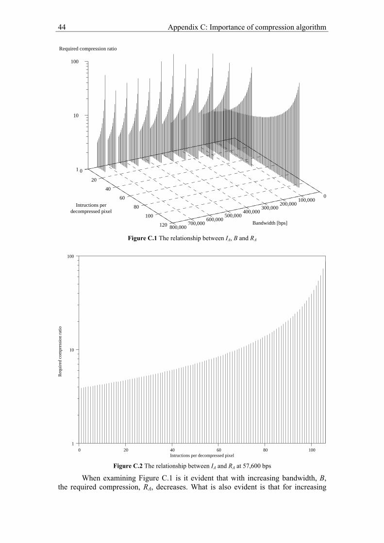
44 Appendix C: Importance of compression algorithm
0
20
40
60
80
100
120
0
Bandwidth [bps]
1
10
100
Required compression ratio
Intructions perdecompressed pixel
800,000 700,000
600,000 500,000
400,000 300,000
200,000 100,000
Figure C.1 The relationship between IA, B and RA
1
10
100
0 20 40 60 80 100
Req
uire
d co
mpr
essi
on r
atio
Intructions per decompressed pixel Figure C.2 The relationship between IA and RA at 57,600 bps
When examining Figure C.1 is it evident that with increasing bandwidth, B, the required compression, RA, decreases. What is also evident is that for increasing
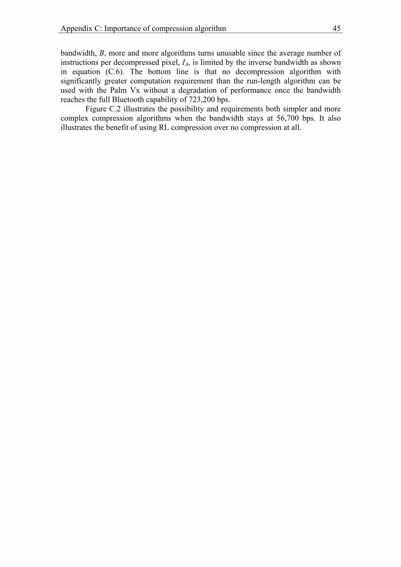
Appendix C: Importance of compression algorithm 45
bandwidth, B, more and more algorithms turns unusable since the average number of instructions per decompressed pixel, IA, is limited by the inverse bandwidth as shown in equation (C.6). The bottom line is that no decompression algorithm with significantly greater computation requirement than the run-length algorithm can be used with the Palm Vx without a degradation of performance once the bandwidth reaches the full Bluetooth capability of 723,200 bps.
Figure C.2 illustrates the possibility and requirements both simpler and more complex compression algorithms when the bandwidth stays at 56,700 bps. It also illustrates the benefit of using RL compression over no compression at all.

Appendix D: I2C 47
Appendix D: I2C
In the I2C standard one master device communicates with one or more slave devices. Each slave has two addresses: one for writing data to it and one for reading data from it. In the I2C standard there are two signal lines, SCLK and SDATA, to which the master and all the slaves are connected. SCLK is controlled by the master and listened to by the slaves. SDATA is listened to by both the master and the slaves. A protocol defines who can signal and when they should do so. The SDATA signal is by default pulled up to logic 1 and is thus only pulled down during the signalling.
The protocol
The I2C bus defines the following different transmission codes which together forms the communication protocol.
A start bit: SDATA is pulled low while SCLK remains high. A slave device’s 8-bit address: SDATA’s state on SCLK’s positive flank
defines the logic value. Most significant bit is transferred first. An acknowledge bit: The receiving device pulls the SDATA low while the
transmitting device releases the SDATA signal for a SCLK clock pulse. If the SDATA is not pulled down during the SCLK clock pulse is a no-acknowledge signal generated.
An 8-bit message: SDATA’s state on SCLK’s positive flank defines the logic value. Most significant bit is transferred first.
A stop bit: SDATA transition from low to high while SCLK remains high. Bus idle: both SCLK and SDATA remain high after a stop bit.
Communication is always initiated by the master sending a start bit. If the master wishes to write to a slave it sends the slave’s 8-bit writing address. When the slave recognizes its address, it signals an acknowledge bit. The master then sends an 8-bit message which contains the register the master is concerned with and the slave responds with an acknowledge bit. The master then writes 8-bit messages and the slave acknowledges until the master sends a stop bit or a new start bit. For each acknowledged 8-bit message is the slave’s register address automatically incremented.
If the master wishes to read from a slave it transmits the slave’s 8-bit writing address followed by the register of interest as in the normal writing case. When both sets of data have been acknowledged by the slave the master sends the slave’s 8-bit reading address. The slave acknowledges and starts outputting the content of the previously selected register. While the master acknowledges the slave continues sending the content of successive registers. The read is terminated by the master if no acknowledge bit is sent or either a stop or a new start bit is sent.

48 Appendix D: I2C
Appendix E: Run-length compression 49
Appendix E: Run-length compression
Run length compression is a simple, fix width compression algorithms. It is particularly well suited for repetitive data. In the code, each entry contain n bits of which d bits are used the replicate the original datablock. The remaining k bits describe how many identical datablocks immediately follow the original datablock. The maximum attainable compression ratio thus becomes:
kd
dRk
MAX +⋅
=2 (E.1)
More important, however, is the achieved compression ratio which is largely dependent on the original data and the chosen values for k and d.

50 Appendix E: Run-length compression
På svenska
Detta dokument hålls tillgängligt på Internet – eller dess framtida ersättare –under en längre tid från publiceringsdatum under förutsättning att inga extra-ordinära omständigheter uppstår.
Tillgång till dokumentet innebär tillstånd för var och en att läsa, ladda ner,skriva ut enstaka kopior för enskilt bruk och att använda det oförändrat för ick-ekommersiell forskning och för undervisning. Överföring av upphovsrätten viden senare tidpunkt kan inte upphäva detta tillstånd. All annan användning avdokumentet kräver upphovsmannens medgivande. För att garantera äktheten,säkerheten och tillgängligheten finns det lösningar av teknisk och administrativart.Upphovsmannens ideella rätt innefattar rätt att bli nämnd som upphovsman i denomfattning som god sed kräver vid användning av dokumentet på ovan beskrivnasätt samt skydd mot att dokumentet ändras eller presenteras i sådan form eller isådant sammanhang som är kränkande för upphovsmannens litterära eller konst-närliga anseende eller egenart.
För ytterligare information om Linköping University Electronic Press se för-lagets hemsidahttp://www.ep.liu.se/
In English
The publishers will keep this document online on the Internet - or its possiblereplacement - for a considerable time from the date of publication barring excep-tional circumstances.
The online availability of the document implies a permanent permission foranyone to read, to download, to print out single copies for your own use and touse it unchanged for any non-commercial research and educational purpose. Sub-sequent transfers of copyright cannot revoke this permission. All other uses ofthe document are conditional on the consent of the copyright owner. The pub-lisher has taken technical and administrative measures to assure authenticity,security and accessibility.
According to intellectual property law the author has the right to be men-tioned when his/her work is accessed as described above and to be protectedagainst infringement.
For additional information about the Linköping University Electronic Pressand its procedures for publication and for assurance of document integrity, pleaserefer to its WWW home page:http://www.ep.liu.se/
© Robert Risberg