Caller Line Identification
26
1 DEPARTMENT OF ELECTRONICS AND COMMUNICATIONS MAR ATHANASIUS COLLEGE OF ENGINEERING KOTHAMANGALAM MINI PROJECT REPORT-2010 CALLER LINE IDENTIFICATION GUIDED BY SUBMITTED BY Mr. AJI JOY (LECTURER IN ECE) ANGELO KURIAN DEPT OF REG NO: 50363 ELECTRONICS & COMMUNICATION
-
Upload
angelo-kurian -
Category
Documents
-
view
232 -
download
0
Transcript of Caller Line Identification

8/6/2019 Caller Line Identification
http://slidepdf.com/reader/full/caller-line-identification 1/261
DEPARTMENT OF ELECTRONICS AND COMMUNICATIONS
MAR ATHANASIUS COLLEGE OF
ENGINEERING
KOTHAMANGALAM
MINI PROJECT REPORT-2010
CALLER LINE IDENTIFICATION
GUIDED BY SUBMITTED BY
Mr. AJI JOY (LECTURER IN ECE) ANGELO KURIAN
DEPT OF REG NO: 50363
ELECTRONICS & COMMUNICATION
8/6/2019 Caller Line Identification
http://slidepdf.com/reader/full/caller-line-identification 2/262
MAR ATHANASIUS COLLEGE OF
ENGINEERING
KOTHAMANGALAM
CALLER LINE IDENTIFICATION
Bonafide Record of Mini Project done by
ANGELO KURIAN
Reg No: 50363
Dissertation submitted in partial fulfillment of the
Requirements for the degree of
BACHELOR OF TECHNOLOGY
Branch: ELECTRONICS AND COMMUNICATION
Of M.G. University
April-May 2010
Date:…………….
EXTERNAL EXAMINER FACULTY GUIDE

8/6/2019 Caller Line Identification
http://slidepdf.com/reader/full/caller-line-identification 3/263
ACKNOWLEDGEMENT
First and foremost, I would like to express my sincere gratitude to my
project guide, Mr.Aji Joy. I was privileged to experience a sustained
enthusiastic and involved interest from his side.
I would also like to thank my seniors who were ready with a positive
comment all the time, whether it was an off-hand comment to encourage
us or a constructive piece of criticism and a special thank to Mr.Jiss Paul
who helped us to clear our various doubts regarding the project.
I thank our HOD Prof.Thomas George providing all the facilities which
helped us to successfully complete the project.
I also thank Ms.Surekha M ,HOD of the CS Department and also Ms.Jiso
George of the CS Dept for providing their lab for the demonstration of
our project
Last but not least, I would like to thank the Electronics and
communication department and the institute, in general, for extending a
helping hand at every juncture of need.
8/6/2019 Caller Line Identification
http://slidepdf.com/reader/full/caller-line-identification 4/264
CONTENTS
1. Introduction 5
2. Working Principle 6
3. Block Diagram 8
4. Circuit Diagram 9
5. Circuit Explanation 10
6. Program Section 13
7. PCB Layout 21
8. Components Used 23
9. Softwares Used 24
10. Conclusion 25
11. Reference 26
12. Datasheets 27

8/6/2019 Caller Line Identification
http://slidepdf.com/reader/full/caller-line-identification 5/265
INTRODUCTION
Caller ID (caller identification, CID), also called calling line
identification (CLID) or calling number identification (CNID), is a
telephone service, available in analog and digital phone systems and most
Voice over Internet Protocol (VoIP) applications, that transmits a caller's
number to the called party's telephone equipment during the ringing
signal, or when the call is being set up but before the call is answered.
This feature can be useful for example for storing numbers of the people
who have tried to call you when you were not home. This feature is
nowadays activated so that the caller number is transferred always to the
telephone central near called person. If the called person wants to get that
information, he/she must order this service from Telephone Company.
Where available, caller ID can also provide a name associated with the
calling telephone number. The information made available to the called
party may be displayed on a telephone's display or on a separately
attached device.
Caller ID may be used to track down or limit the impact of telemarketers,
prank calls, and other intrusions. However, it can also impede
communication by enabling users to become evasive. The concept behind
caller ID is the value of informed consent
It has enhanced the sense of privacy enjoyed by persons in their homes,
and has also greatly reduced the number of prank calls, as well as calls
made with threatening or criminal intent.
8/6/2019 Caller Line Identification
http://slidepdf.com/reader/full/caller-line-identification 6/266
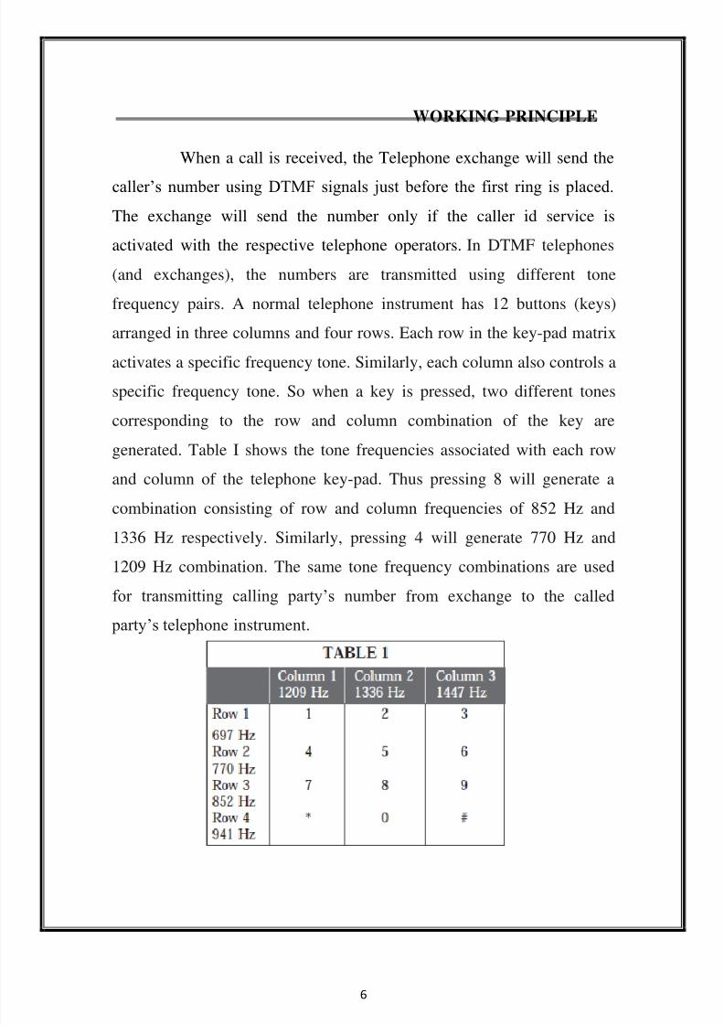
WORKING PRINCIPLE
When a call is received, the Telephone exchange will send the
caller’s number using DTMF signals just before the first ring is placed.
The exchange will send the number only if the caller id service is
activated with the respective telephone operators. In DTMF telephones
(and exchanges), the numbers are transmitted using different tone
frequency pairs. A normal telephone instrument has 12 buttons (keys)
arranged in three columns and four rows. Each row in the key-pad matrix
activates a specific frequency tone. Similarly, each column also controls a
specific frequency tone. So when a key is pressed, two different tones
corresponding to the row and column combination of the key are
generated. Table I shows the tone frequencies associated with each row
and column of the telephone key-pad. Thus pressing 8 will generate a
combination consisting of row and column frequencies of 852 Hz and
1336 Hz respectively. Similarly, pressing 4 will generate 770 Hz and
1209 Hz combination. The same tone frequency combinations are used
for transmitting calling party’s number from exchange to the called
party’s telephone instrument.
8/6/2019 Caller Line Identification
http://slidepdf.com/reader/full/caller-line-identification 7/267
The DTMF decoder decodes each set of frequency pairs representing the
number and the number is available as binary at the output pins of the
decoder when the TOE pin is made high. After decoding each pair of DTMF frequencies the StD pin of the decoder goes high and interrupts
the microcontroller. The output pins of the DTMF decoder are connected
to the port A of the microcontroller. After each interrupt the decoded
number is stored in a register in the microcontroller, once all the numbers
are received, the number is displayed on the LCD. After displaying the
caller’s number on the LCD the number is stored in the internal
EEPROM of the Microcontroller, so that the received number can be
reviewed later. By Pressing RB4 display mode can accessed, By pressing
RB5 you can cycle through the received calls, Pressing RB4 again exits
the display mode.By Pressing RB6 Previous entries can be cleared.When
the memory is full newly received number automatically replaces the
oldest entry in the memory.
8/6/2019 Caller Line Identification
http://slidepdf.com/reader/full/caller-line-identification 8/268
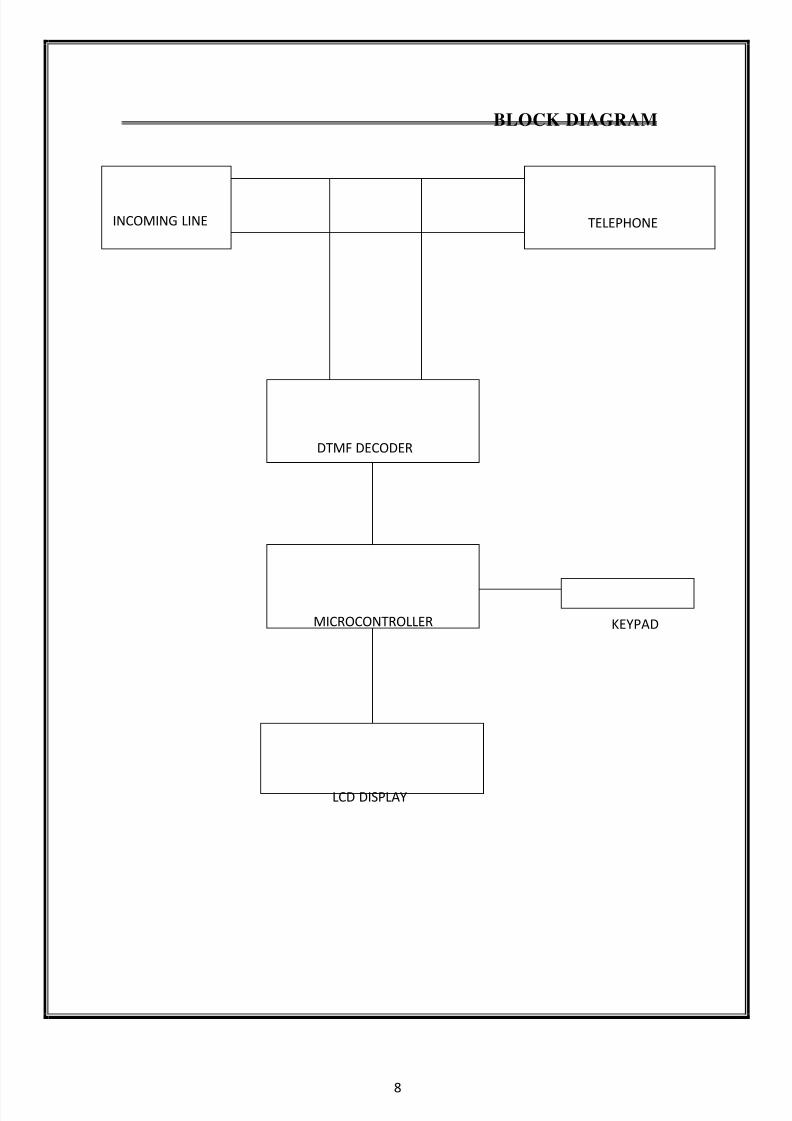
BLOCK DIAGRAM
TELEPHONE
DTMF DECODER
MICROCONTROLLER KEYPAD
LCD DISPLAY
INCOMING LINE
8/6/2019 Caller Line Identification
http://slidepdf.com/reader/full/caller-line-identification 9/269
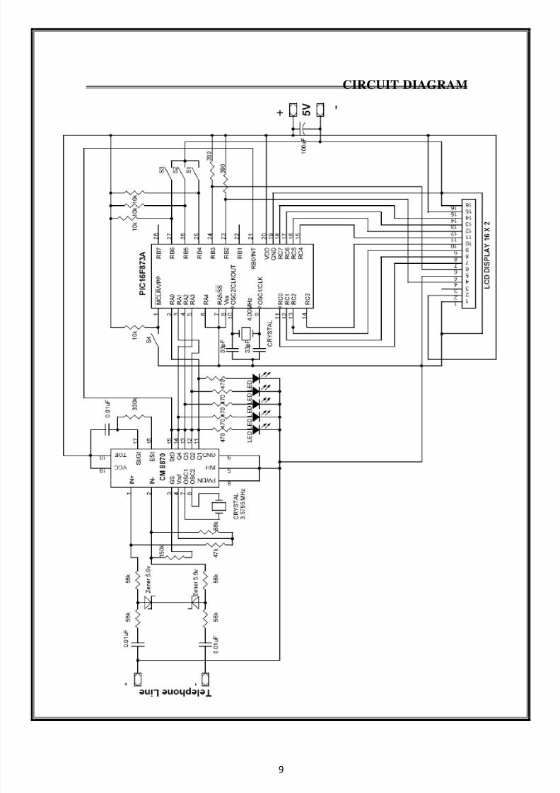
CIRCUIT DIAGRAM
8/6/2019 Caller Line Identification
http://slidepdf.com/reader/full/caller-line-identification 10/2610
CIRCUIT EXPLANATION
POWER SUPPLY
The power is supplied using a 5V DC adapter
DTMF DECODER SECTION
It consists of the CM8870 DTMF Decoder.DTMF decoder CM8870 is
AC coupled to telephone lines and keeps on sensing tone frequencies.
The circuit is configured in balanced line mode. To reject common-mode
noise signals, a balanced differential amplifier input is used. The circuit
also provides an excellent bridging interface across a properly terminated
telephone line. Transient protection may be achieved by splitting the
input resistors and inserting zener diodes (ZD1 and ZD2) to achieve
voltage clamping. This allows the transient energy to be dissipated in the
resistors and diodes, and limits the maximum voltage that may appear at
the inputs. As soon as a valid DTMF digit is detected, it sets StD pin (Pin
15) high and interrupts the micro-controller. DTMF decoder also requires
a Micro-controller which then reads the digital number on four data lines
(D4-D7).The output of the DTMF Decoder can be viewed on the LED’s
Connected to the output pins.
8/6/2019 Caller Line Identification
http://slidepdf.com/reader/full/caller-line-identification 11/2611
MICROCONTROLLER SECTION
It Consists of the PIC 16F873A Microcontroller. The First pin of the
Microcontroller is connected to the Vcc through a resistor and to the
ground through a switch. The switch acts a reset switch which resets the
microcontroller. The Microcontroller has three ports, Port A is connected
to the output pins of the DTMF decoder (RA0 to RA3). Three switches
are connected to PORT B , the switches are for reviewing the numbers of
the previously received calls. The control pins of the LCD are also
connected to PORT B (RS, R/W, and EN). The output of the pins
connected to the switches S1 to S3 are pulled high using pull-up resistors.
The StD pin of the DTMF decoder which is used to interrupt the
microcontroller is connected to RB0/INT pin (pin 21). The Port C is
connected to the data lines of the LCD.
DISPLAY SECTION
The Display Section Uses a 16 X 2 LCD Display Unit to display and
review the received numbers
LCD display unit: LCD display is a Double-line, 16-character unit.Interface with microcontroller is accomplished via eight data lines D7-D0
and two control lines RS and E. Using these six lines, micro-controller
displays all messages and telephone numbers.
LCD controller is a flexible controller and can be used with 8-bit or 4-bit
micro-controller. In 4-bit mode, only D4-D7 is used, leaving D0-D3
open. In our circuit, we have connected R/W pin to ground as we areusing it for write operation only. Reading back of the module’s status,

8/6/2019 Caller Line Identification
http://slidepdf.com/reader/full/caller-line-identification 12/2612
which is required to see if LCD module is busy, is not possible. To avoid
problems, extra delays in software are provided after every write
command so that before writing another command/data, LCD module
should be ready (not busy). Here the LCD is used in 8 bit mode.
8/6/2019 Caller Line Identification
http://slidepdf.com/reader/full/caller-line-identification 13/2613
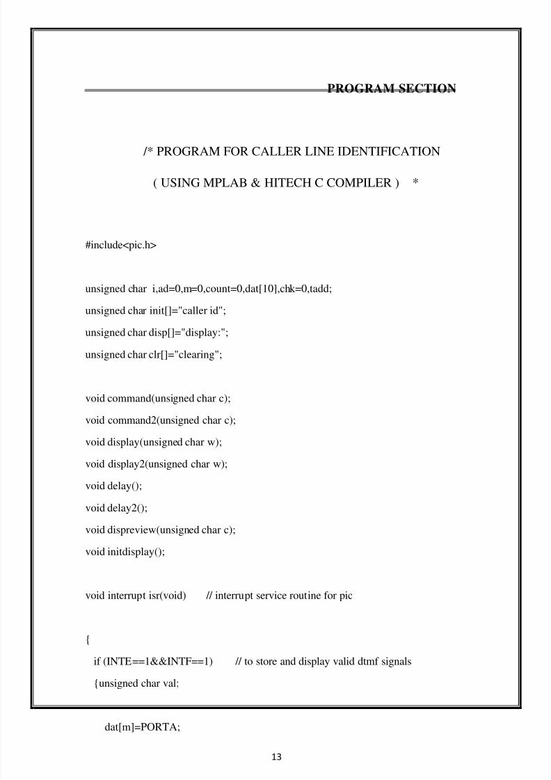
PROGRAM SECTION
/* PROGRAM FOR CALLER LINE IDENTIFICATION
( USING MPLAB & HITECH C COMPILER ) *
#include<pic.h>
unsigned char i,ad=0,m=0,count=0,dat[10],chk=0,tadd;
unsigned char init[]="caller id";
unsigned char disp[]="display:";
unsigned char clr[]="clearing";
void command(unsigned char c);
void command2(unsigned char c);
void display(unsigned char w);
void display2(unsigned char w);
void delay();
void delay2();
void dispreview(unsigned char c);
void initdisplay();
void interrupt isr(void) // interrupt service routine for pic
{
if (INTE==1&&INTF==1) // to store and display valid dtmf signals
{unsigned char val;
dat[m]=PORTA;
8/6/2019 Caller Line Identification
http://slidepdf.com/reader/full/caller-line-identification 14/2614
m++;
if(m==11) // to check whether full number is received
{command(0x01);
delay();
for(i=0;i<m;i++) // displaying number on lcd
{val=dat[i]&0x0F;
if(val==0x0A)
{
val=0x30;
}
else
{
val=val|0x30;
}
display(val);
delay();
}
ad=eeprom_read(EEPROM_SIZE-1); /* current memory location in eeprom is
stored in last location of eeprrom */
for(i=0;i<m;i++) // storing number in eeprom
{ val=dat[i]&0x0F;
if(val==0x0A)
{
val=0x30;
}
else

8/6/2019 Caller Line Identification
http://slidepdf.com/reader/full/caller-line-identification 15/2615
{
val=val|0x30;
}
eeprom_write(ad,val);
ad++;
if(i==(m-1))
eeprom_write((EEPROM_SIZE-1),ad); // updating stored memory location
}
if(ad>=0x6F)
eeprom_write((EEPROM_SIZE-1),0x00); // for resetting on overflow
m=0;
}
INTF=0;
}
if( RBIF==1&&RBIE==1 ) // PORTB interrupt used for displaying previous no.s
{
if( RB4==0 )
{ chk++;
if( chk>1 )
{chk=0;
initdisplay();
}
tadd=(eeprom_read(EEPROM_SIZE-1));
if( chk==1 )
8/6/2019 Caller Line Identification
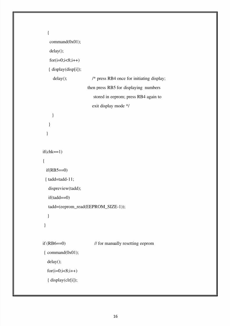
http://slidepdf.com/reader/full/caller-line-identification 16/2616
{
command(0x01);
delay();
for(i=0;i<8;i++)
{ display(disp[i]);
delay(); /* press RB4 once for initiating display;
then press RB5 for displaying numbers
stored in eeprom; press RB4 again to
exit display mode */
}
}
}
if(chk==1)
{
if(RB5==0)
{ tadd=tadd-11;
dispreview(tadd);
if(tadd==0)
tadd=(eeprom_read(EEPROM_SIZE-1));
}
}
if (RB6==0) // for manually resetting eeprom
{ command(0x01);
delay();
for(i=0;i<8;i++)
{ display(clr[i]);
8/6/2019 Caller Line Identification
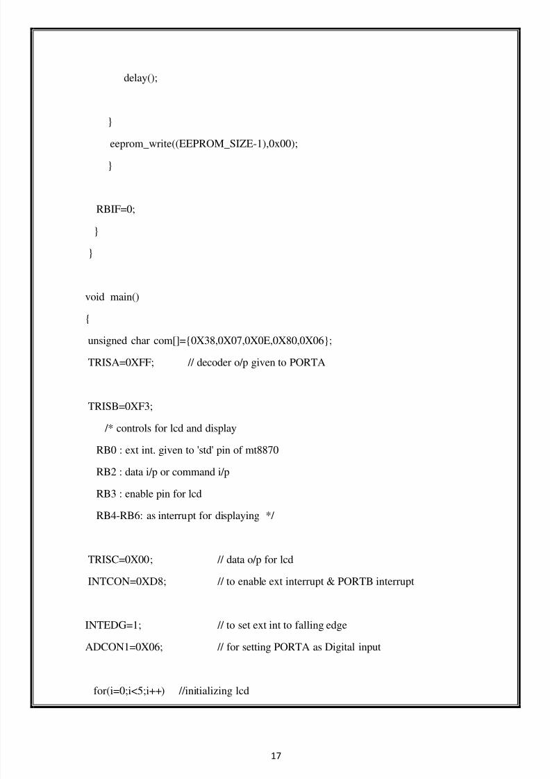
http://slidepdf.com/reader/full/caller-line-identification 17/2617
delay();
}
eeprom_write((EEPROM_SIZE-1),0x00);
}
RBIF=0;
}
}
void main()
{
unsigned char com[]={0X38,0X07,0X0E,0X80,0X06};
TRISA=0XFF; // decoder o/p given to PORTA
TRISB=0XF3;
/* controls for lcd and display
RB0 : ext int. given to 'std' pin of mt8870
RB2 : data i/p or command i/p
RB3 : enable pin for lcd
RB4-RB6: as interrupt for displaying */
TRISC=0X00; // data o/p for lcd
INTCON=0XD8; // to enable ext interrupt & PORTB interrupt
INTEDG=1; // to set ext int to falling edge
ADCON1=0X06; // for setting PORTA as Digital input
for(i=0;i<5;i++) //initializing lcd
8/6/2019 Caller Line Identification
http://slidepdf.com/reader/full/caller-line-identification 18/2618
{command2(com[i]);
delay2();
}
command2(0x01);
delay2();
for(i=0;i<9;i++)
{display2(init[i]);
delay2();
}
while(1) // infinite loop
{
delay2();
}
}
void command(unsigned char a) // for giving commands to lcd
{
RB2=0;
PORTC=a;
RB3=1;
RB3=0;
}
void command2(unsigned char a) // for giving commands to lcd
{
RB2=0;
PORTC=a;
RB3=1;
8/6/2019 Caller Line Identification
http://slidepdf.com/reader/full/caller-line-identification 19/2619
RB3=0;
}
void delay() // delay reqiured for writing into lcd
{
unsigned char b,c;
for(b=0;b<255;b++)
for(c=0;c<255;c++);
}
void delay2() // delay reqiured for writing into lcd
{
unsigned char b,c;
for(b=0;b<255;b++)
for(c=0;c<255;c++);
}
void display(unsigned char a) // to display the argument in lcd
{
RB2=1;
PORTC=a;
RB3=1;
RB3=0;
}
void display2(unsigned char a) // to display the argument in lcd
{
RB2=1;
PORTC=a;
8/6/2019 Caller Line Identification
http://slidepdf.com/reader/full/caller-line-identification 20/2620
RB3=1;
RB3=0;
}
void dispreview(unsigned char c) // to display numbers from eeprom
{ unsigned char y;
command(0x01);
delay();
for(y=0;y<11;y++)
{display(eeprom_read(c+y));
delay();
}
}
void initdisplay() // to display "caller id" on lcd
{unsigned char e;
command(0x01);
delay();
for(e=0;e<9;e++)
{display(init[e]);
delay();
}
}
8/6/2019 Caller Line Identification
http://slidepdf.com/reader/full/caller-line-identification 21/2621
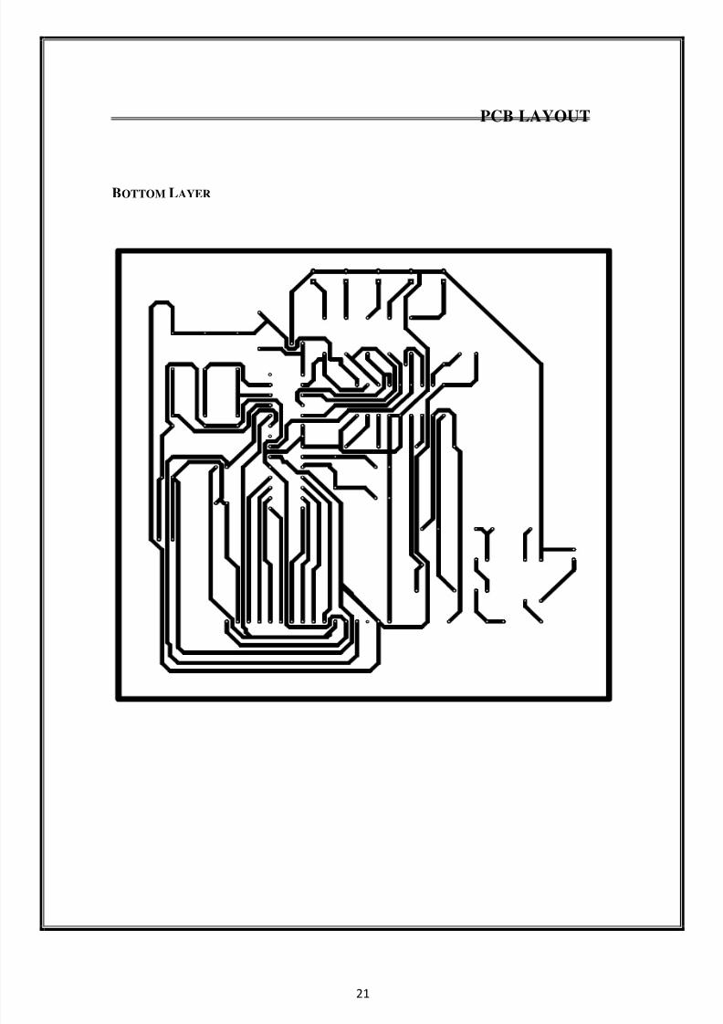
PCB LAYOUT
BOTTOM LAYER

8/6/2019 Caller Line Identification
http://slidepdf.com/reader/full/caller-line-identification 22/2622
TOP LAYER
8/6/2019 Caller Line Identification
http://slidepdf.com/reader/full/caller-line-identification 23/2623
COMPONENTS USED
1.PIC 16F873A Microcontroller
2.CM8870 DTMF Decoder
3.16 X 2 LCD Module
4.Crystal
5.Zener Diodes
6.LED’s
7.Resistors
8.Capacitors
9.Push Switches

8/6/2019 Caller Line Identification
http://slidepdf.com/reader/full/caller-line-identification 24/2624
SOFTWARES USED
1. Microchip MPLAB
2. Orcad Capture
3. Orcad Layout Plus
4. Pic Simulator
8/6/2019 Caller Line Identification
http://slidepdf.com/reader/full/caller-line-identification 25/2625
CONCLUSION
The project entitled “CALLER LINE IDENTIFICATION” has been
designed and developed successfully. The PCB layout is also
created. The project was completed successfully within the
stipulated time, tested and verified.
8/6/2019 Caller Line Identification
http://slidepdf.com/reader/full/caller-line-identification 26/26
REFERENCES
1. www.microchip.com
2. www.calmicro.com
3. www.picbasic.nl
4. www.epanorama.net
5. www.efy.com