Call for Paper 2 0 0 5 SOLID STATE DEVICES AND · PDF fileon Solid State Devices and Materials...
24
S OLID S TATE D EVICES AND M ATERIALS INTERNATIONAL CONFERENCE ON 2005 International Conference on Solid State Devices and Materials (SSDM 2005) Web Site : http://www.ssdm.jp 2 0 0 5 Call for Paper Conference Short Course Place September 13-15, 2005 September 12, 2005 International Conference Center Kobe (Hyogo, Japan) Paper Deadline May 12, 2005 Late News Paper Deadline July 29, 2005 Sponsored by THE JAPAN SOCIETY OF APPLIED PHYSICS Technical-Cosponsored by IEEE Electron Devices Society in cooperation with The Electrochemical Society of Japan IEEE EDS Japan Chapter IEEE Japan Council The Institute of Electrical Engineers of Japan The Institute of Electronics, Information and Communication Engineers The Institute of Image Information and Television Engineers Japan Institute of Electronics Packaging 2005 SECRETARIAT c/o Inter Group Corp. Toranomon Takagi Bldg., 1-7-2, Nishishinbashi, Minato-ku, Tokyo 105-0003 Japan TEL:+81-3-3597-1108 FAX:+81-3-3597-1097 E-mail: [email protected] Online submission through the conference website is now available.
Transcript of Call for Paper 2 0 0 5 SOLID STATE DEVICES AND · PDF fileon Solid State Devices and Materials...

SOLID STATEDEVICES AND MATERIALS
INTERNATIONAL CONFERENCE ON
2005 International Conference on Solid State Devices and Materials (SSDM 2005)
Web Site : http://www.ssdm.jp
2 0 0 5
Call for Paper
Conference
Short Course
Place
September 13-15, 2005September 12, 2005International Conference Center Kobe(Hyogo, Japan)
Paper Deadline May 12, 2005
Late News Paper Deadline July 29, 2005Sponsored byTHE JAPAN SOCIETY OF APPLIED PHYSICSTechnical-Cosponsored byIEEE Electron Devices Societyin cooperation withThe Electrochemical Society of JapanIEEE EDS Japan ChapterIEEE Japan CouncilThe Institute of Electrical Engineers of JapanThe Institute of Electronics, Information and Communication EngineersThe Institute of Image Information and Television EngineersJapan Institute of Electronics Packaging
2005
SECRETARIAT c/o Inter Group Corp. Toranomon Takagi Bldg., 1-7-2, Nishishinbashi, �Minato-ku, Tokyo 105-0003 JapanTEL:+81-3-3597-1108FAX:+81-3-3597-1097E-mail: [email protected] Online submission through the conference website
is now available.

Call for Papers
2005 INTERNATIONAL CONFERENCE ONSOLID STATE DEVICES AND MATERIALS
Conference: September 13-15, 2005Short Course (in Japanese): September 12, 2005
The 2005 International Conference on Solid State Devicesand Materials (SSDM 2005) will be held from September13 to September 15, 2005 at International ConferenceCenter Kobe (Hyogo, Japan). Since 1969, the conferencehas provided an excellent opportunity to discuss keyaspects of solid-state devices and materials. For the 2005conference, 11 program subcommittees have beenorganized covering circuits and systems, as well asdevices and materials. A one-day short course is alsoscheduled prior to the conference, offering tutoriallectures on important aspects of the technology.
Original, unpublished papers will be accepted after reviewby the Program Committee. Several invited speakers willcover topics of current interest. An Advance Program willappear in July. More information about SSDM 2005 isavailable online at:
http://www. ssdm.jp
— 1 —

PLENARY SESSIONSPlenary Speakers:“Development of Clinical Chips for Home MedicalDiagnostics” (tentative)
Y. Horiike (NIMS, Japan)“Carbon Nanotube Electrical & Optical Devices”
P. Avouris (IBM, USA)
SCOPE OF CONFERENCEThe conference aims at providing a forum for synergisticinteractions among research scientists and engineersworking in the fields related to solid state devices andmaterials and encouraging them to discuss problems to besolved in these fields, new findings, new phenomena, andstate-of-the-art technologies related to devices andmaterials. The conference also aims to facilitate mutualunderstanding among people in the device and materialfields and those in the circuit, system and packagingfields. For the 2005 conference, eleven programsubcommittees have been organized in order to realizeselection of higher quality papers and strengthen specifictechnology areas. The scope of each subcommittee islisted below.
Area 1Advanced Gate Stack/Si Processing Science
(Chair: Y. Nara, Selete)This subcommittee covers all the innovative front-end-of-line process technologies for advanced silicon-based LSIdevices. Papers are solicited in the following areas (butare not limited to these areas): (1) advanced gate stacktechnologies, such as a SiON gate insulator, high-k gateinsulator, and metal gate technologies, including deviceintegration technology; (2) front-end-of-line processtechnologies that break through the scaling limit, such as alow-temperature process, shallow junction formation,novel diffusion/oxidation, and high-precision etching; (3)reliability physics and analysis; and (4) characterizationand modeling of a Si process.
Invited speakers:“Advanced Gate Stack Technology –Present Status andChallenges–” (tentative)
M. Niwa (Matsushita Electric, Japan)
— 2 —

“Current Status and Forecast toward hp45nm Node inCMOS Technology” (tentative)
T. Sugii (Fujitsu, Japan)“Material and Process Characterization for Future CMOSTechnology” (tentative)
S. Zaima (Nagoya Univ., Japan)
Area 2Characterization and Materials Engineering for DeviceIntegration
(Chair: S. Ogawa, Matsushita Electric)In this session, technologies and sciences that cover a Siback-end-of-line process are discussed, including packagetechnology. Low-k materials have been in practical use;however, they brought new, difficult issues withdecreasing in size, especially in reliability and packageareas, and these areas require different ideas fromconventional interconnect in characterization, material,and process/structure technologies. Papers are solicited inthe following areas (but are not limited to these areas): (1)characterization methodology for materials, mechanicaland electrical properties in small geometry, and yieldimprovement; (2) materials and process technologies foradvanced Cu/Low-k interconnect, including new dielectricand metal formation, planarization, and etching; (3)reliability phenomena and physics, such as EM, SIV,TDDB, and modeling/prediction; (5) packaging forCu/Low-k chips; (4) new concepts and materials for futureinterconnects, such as a 3-D structure, a CNTinterconnect, and wireless applications.
Invited speakers:“Integration Challenges for Carbon Nanotubes”
F. Kreupl (Infineon, Germany)“Cu/Low-k Process Integration for 65nm and 45nm SoCDevices”
N. Matsunaga (Toshiba, Japan)“Nm-Order Structures of Porous Low-k Film and its Impacton Cu/Low-k Process”
M. Shimada (Selete, Japan)
Area 3CMOS Devices/Device Physics
(Chair: K. Shibahara, Hiroshima Univ.)The aim of this area is to discuss advanced silicon device
— 3 —

technologies and physics. Papers are solicited in thefollowing areas: (1) sub-100-nm silicon CMOS devicesand their integration technologies; (2) performanceenhancement technologies, such as a strained-siliconchannel and SiGe and Ge channels; (3) post-bulk-planarsilicon device structures, including planar SOI, FinFET,and double gate FET; (4) device physics of advancedCMOS, including simulation and modeling on carriertransport and reliability; and (5) manufacturing and yieldscience.
Invited speakers:“Perspective on Emerging CMOS Devices and theirImpact on Scaling Technologies” (tentative)
S. Biesemans (IMEC, Belgium)“45nm Conventional Bulk and Bulk+ Architectures forLow Cost GP/LP Applications” (tentative)
F. Boeuf (ST Microelectronics, France)“Investigation of NBTI in Ultra-Thin Oxide p-MOSFETs”(tentative)
S. Mahapatra (IIT Bombay, India)
Area 4Advanced Memory Technology
(Chair: A. Nitayama, Toshiba)Advanced memory technologies are very much expectedto explosively evolve SoC devices and digital informationtechnologies toward “high speed and high density,broadband and mobile.” Papers are solicited in the area ofall advanced volatile or nonvolatile memory devices, suchas DRAM, flash (including SONOS and nanocrystaldevices), FeRAM, MRAM, phase change RAM,resistance RAM, one time programming memory, 3-Dmemory, and others. Topics include cell device physicsand characterization, process integration and materials,tunneling dielectrics, ferroelectric and ferromagneticmaterials, reliability, failure analysis, quality assuranceand testing, modeling and simulation, process control andyield enhancement, integrated circuits, new conceptmemories, and new applications and systems (solid statedisks, memory cards, programmable logic, etc.).
Invited speakers:“Overview and Future Challenges of MONOSTechnologies”
T. Ishimaru (Hitachi, Japan)
— 4 —

“Current Development Status and Future Challenge ofFeRAM Technologies” (tentative)
S. Y. Lee (Samsung Electronics, Korea)“Physical and Microscopic Understanding of DataRetention Time of DRAM”
K. Okonogi (Elpida, Japan)“Overview and Future Challenge of MRAM Technologies”
S. Tehrani (Freescale, USA)
Area 5Advanced Circuits and Systems
(Chair: H. Kobayashi, Gunma Univ.)Original papers bridging the gap between materials,devices, circuits, and systems in Si-ULSI, including SiGe,are solicited in subject areas that include, but not limitedto the following: (1) advanced digital, analog, mixed-signal circuits as well as memory; (2) high-speed andhigh-frequency circuits; (3) wireless, wireline, and opticalcommunication; (4) power management technology; (5)interconnection design for communication inside a chip aswell as among chips; (6) technologies for systems on achip (SoC) and system in a package (SiP); and (7) LSItesting technology.
Invited speakers:“Design and Architecture Exploration for Image andVideo Coding Systems”
L.-G. Chen (National Taiwan Univ., Taiwan)“Issues of Mixed-Signal Circuit Design in 90nm CMOSLSI Technology”
T. Iida (Toshiba, Japan)“The High Voltage Anti-Trend”
C. Mangelsdorf (Analog Devices Inc., Japan)
Area 6Compound Semiconductor Circuits, Electron Devicesand Device Physics
(Chair: M. Kuzuhara, Univ. of Fukui) This session covers all aspects of advanced electrondevice and IC technologies based on compoundsemiconductors, including III-V, III-N, SiC, and othermaterials. Papers are solicited in the following areas: (1)FETs, HFETs, HBTs, and other novel device structures;(2) high-voltage or high-temperature electron devices andcircuits; (3) microwave and millimeter-wave amplifiers,
— 5 —

oscillators, switches, and other ICs; (4) high-speed digitalICs and mixed-signal ICs; (5) theory and physics ofelectron devices; (6) characterization techniques fordevices and ICs; (7) innovative device processing andpackaging; (8) reliability issues; and (9) novel applicationsutilizing compound semiconductor devices and circuits.Contributions related to other interesting topics are alsowelcome.
Invited speakers:“Insulated and Recessed Gate A1N/GaN/InN-basedHEMTs on Different Substrates”
M. Shur (Rensselaer Polytechnic Inst., USA)“Circuit Design for Super-Scaled InP HBTs” (tentative)
J. F. Jensen (Hughes Res. Labs., USA)“Simulation of AlGaN/GaN Heterostructure Field EffectTransistors”
R. Mickevicius (Integrated Systems Engineering Inc.,USA)
“Power Device Application of AlGaN/GaN HFETs on aSi Substrate”
T. Egawa (Nagoya Inst. of Tech., Japan)
Area 7Photonic Devices and Device Physics
(Chair: M. Sugawara, Univ. of Tokyo)The scope of this subcommittee covers all aspects ofemerging technologies in active, passive, and integratedoptoelectronic and photonic devices as well as devicephysics, which include: (1) laser diodes, LEDs,photodetectors, SOAs, and OEICs; (2) quantumnanostructure optical devices including quantum wells,quantum wires, or quantum dots; (3) photonic crystalmaterials and novel functional devices; (4) opticalswitches, modulators, and MEMS; (5) optical wavelengthconverters, nonlinear optical devices, and all-opticalswitches; (6) waveguide components, PLCs and integratedphotonic circuits; (7) material and device processing andcharacterization techniques; (8) hybrid and monolithicintegration, packaging and moduling; (9) opticalcommunication, interconnection and signal processingapplications of optoelectronic and photonic devices; (10)linear and nonlinear optical properties, electronic bandstructures, and the relaxation mechanism of quantumnanostructures; and (11) novel phenomena and
— 6 —

applications including slow light, fast light, opticalmemory, and optoelectronic tweezers, etc.
Invited speakers:“Recent Trend in High-Speed/Low-Power-ConsumptionLight Sources for MAN/Ethernet Applications”
M. Aoki (Hitachi, Japan)“Slow Light Using Semiconductor Quantum Wells andQuantum Dots for Future Optical Networks”
S. L. Chuang (Univ. of Illinois at Urbana-Champaign,USA)
“Exciton-Photon Interactions in a Quantum DotMicrocavity”
A. Forchel (Univ. of Wüerzburg, Germany)
Area 8Advanced Material Synthesis and Crystal GrowthTechnology
(Chair: H. Yamaguchi, NTT)The scope of this subcommittee covers all kinds ofsynthesis, growth, and fabrication techniques of not onlysemiconducting but also novel functional materials andstructures, including spintronic materials, nitridecompounds, CNT, nanowires and nanoparticles, etc. Theprinciple idea is to enhance mutual communication amongpeople in different committees to share knowledge ofcommonly important key technologies in fabricationprocesses. Specific scopes are, but not limited to, thefollowing: (1) novel material systems and structures; (2)materials and structures for spintronics; (3) nitride-relatedcompound semiconductors; (4) novel synthesis, growth,and fabrication techniques; (5) carbon nanotubes; (6)nanowires and nanoparticles; (7) microscale- andnanoscale 3-D structures and mechanical systems; (8)characterization of fundamental properties.
Invited speakers:“Revolution in Carbon Nanotube Synthesis –SuperGrowth–”
D. Futaba (AIST, Japan)“Quantum Dots, Quantum Dot Molecules, and QuantumDot Crystals”
O.G. Schmidt (Max-Planck-Inst., Germany)“Spintronics Based on ZnO Thin Films”
H. Tabata (Osaka Univ., Japan)
— 7 —

“To be announced”Z. K. Tang (Hong Kong Univ. of Sci. & Tech., China)
Area 9Physics and Applications of Novel Functional Materialsand Devices
(Chair: Y. Takahashi, Hokkaido Univ.) This session covers applications and physics of novelfunctional devices and quantum nanostructures that aremade mainly by using nanofabrication technology or self-organized phenomena. Papers are solicited in thefollowing areas (but are not limited to these areas): (1)quantum phenomena in nanostructures; (2) quantum dotsand single-electron devices; (3) solid-state quantumcomputing and communications; (4) spintronics; (5)carbon nanotube devices; (6) nanometer-scalecharacterization, such as SPM and SNOM, other noveldevices, such as small superconducting devices, andresonant tunneling devices in nanoscale.
Invited speakers:“Manipulation and Storage of Charge and Spin inQuantum Dot Devices”
G. Abstreiter (Walter Schottky Inst., Germany)“Fabrication and Demonstration of Quantum-Dot CellularAutomata Systems”
G. H. Bernstein (Univ. of Notre Dame, USA)“Optical Spin-Detection of Quasi-2D Charge Carriers:Experimental Evidence of the Spin Hall Effect”
J. Wunderlich (Hitachi Cambridge Lab., UK)
Area 10Organic Materials Science, Device Physics, andApplications
(Chair: K. Kudo, Chiba Univ.)This field covers organic materials, device physics,characterization, and applications to organic devices.Papers are solicited in the following areas (but are notlimited to these areas): (1) organic transistors and circuits;(2) organic light emitting devices; (3) organic diodes,photodetectors, and photovoltaic devices; (4) chemicalsensors and gas sensors; (5) molecular electronics; (6)fabrication and characterization of organic thin films; (7)electrical and optical properties of organic thin film andmaterials; (8) organic-inorganic hybrid systems; and (9)
— 8 —

interfacial phenomena, LC devices, etc.
Invited speakers:“Organic Semiconductor Field-Effect Transistors andCircuits” (tentative)
J. Kanicki (Univ. of Michigan, USA)“Recent Progresses of Organic Transistor IntegratedCircuits for Large-Area Sensor Applications” (tentative)
T. Someya (Univ. of Tokyo, Japan)“Organic Thin-Film Transistors Based on n-ChannelOrganic Semiconductors” (tentative)
S. Tokito (NHK, Japan)
Area 11Micro/Nano Electromechanical and Bio-Systems
(Chair: H. Tabata, Osaka Univ.) This session focuses on micro/nano electrnomechanicalsystems (MEMS/NEMS) and their applications, such asbiosensors. Bio-M/NEMS devices are widely applied tobiochemical, medical, and environmental fields in whichmany devices are studied, such as biochips, micro-TAS,lab on a chip, etc. Interdisciplinary research ofmicroelectronic devices with materials and technique inthe chemical, biological, and medical fields is expected toopen the door to new scientific and business fields.Papers are solicited in the following areas (but are notlimited to these areas): (1) micro/nano electromechanicalsystems (M/NEMS) for RF, optical, power andbiomaterial fields, and others; (2) micro-TAS and lab on achip; (3) various biochips and sensors; (4) fabricationtechnologies and surface/interface modificationtechniques, such as SAM for micro-TAS and/or biochips;and (5) new integrated micro/nanosystems forbiochemical and medical applications.
Invited speakers:“Bionanotechnology with Membrane Proteins: Mechanicsand Electronics”
S. A. Contera (Univ. of Oxford, UK)“Integrated Microfluidic Systems for Cell and TissueEngineering”
T. Fujii (Univ. of Tokyo, Japan)“Computational 3-D Microfabrication for MEMS”
O. Tabata (Kyoto Univ., Japan)
— 9 —

RUMP SESSIONS Following two Rump Sessions have been organized onSeptember 14 (Wednesday).
Session A“Beyond the Scaling Limit—Innovative Devices andMaterials—”Organizer/Moderator :
Y. Hirayama (NTT, Japan)K. Masu (Tokyo Tech., Japan)
H. Tabata (Osaka Univ., Japan)S. Zaima (Nagoya Univ., Japan)
Within 10 years, device sizes will surely reach less than10 nm and we will then face a problem called the scalinglimit. As we approach or go beyond the scaling limit, weneed innovative concepts in signal transfer andprocessing. We will also have to take into accountquantum effects in addition to classical effects even atroom temperature. In this rump session, we would like todiscuss what will happen in this situation fromtechnological and physical viewpoints and what will benecessary to overcome this near-future problem.Innovative device designs, process technologies andintegration methods will be played up in this rumpsession. The introduction of innovative materials will be akey issue for future devices. Our discussions will not belimited to conventional silicon devices; they will extend tocompound semiconductors and non-silicon basedmaterials, i.e. oxides, carbon based compounds andmolecules, as well. It is our hope that this rump sessionwill get everyone thinking about the scaling-limit and thatthe discussions in this session become a starting point fornew scaling concepts.
Session B“Flexible Electronics –Is it Real?”Organizer:
H. Matsuoka (Hitachi, Japan)Moderator:
To be announced
Special attention has been paid to flexible electronicsbecause of the remarkable progress of device technologiessuch as organic thin-film transistor and semiconductor
— 10 —

nanowire. Recently, many interesting applications havebeen proposed, such as wearable computers, flexibleimage scanners, flexible displays, etc. Flexible electronicshas the potential to offer advantages over existingtechnologies and to open a new market. In this rumpsession, we would like to discuss the following issues;(1) What kind of future does flexible electronics bring
about?(2) When will it become real? (3) What features are required for a device technology?
What are the candidates?(4) What are the technical hurdles to overcome? Where
are we now?We hope you will gain an understanding of the presentstatus and join in the discussion on the future prospects forthis fascinating technology.
SHORT COURSE Short Course entitled “Organic Semiconductor Deviceswith Attractive and Possible Properties” will be held onMonday, September 12. All lectures are given in Japanese.
SUBMISSION OF PAPERSProspective authors must submit a two-page camera-readypaper with all figures and tables to the conference web siteat http://www.ssdm.jp.Please note that submissions by post will NOTbe accepted.
The two-page paper must be prepared in English in 8.5-×11-inch or A4-format and submitted as a PDF file of lessthan 1 megabyte. The first page must include the title ofthe paper, author(s), affiliation(s), address, telephonenumber, fax number, e-mail address, and article text. Thesecond page should be used to indicate figures, tables andphotographs. Detailed format information will be postedon the conference web site. Two-byte characters such asJapanese, Chinese, Korean, etc. fonts cannot be used foreither figures or texts. The paper should report original,previously unpublished work, including specific results.Papers to be presented at the conference will be selectedby each subcommittee on the basis of suggested areas andcontent.
Deadline for Submission is May 12, 2005.
— 11 —

Authors of accepted papers will be notified by e-mailbefore mid-July and requested to give either a 15- to 20-minute oral presentation or a poster presentation.
EXTENDED ABSTRACTS AND PUBLICATIONAccepted papers will be printed, without opportunity forfurther revision, in the extended abstracts that which willbe distributed to conference participants during theconference.
Authors of papers accepted for presentation at SSDM2005 are encouraged to submit the original to the SpecialIssue of the Japanese Journal of Applied Physics, whichwill be published in April, 2006.
AGREEMENT NOT TO PRE-PUBLISH ABSTRACTSBy submitting an abstract to the committee for review, theauthor(s) agrees that the work will not be published priorto presentation at the conference. Papers found to be inbreach of this agreement will be withdrawn by theconference committee.
LATE NEWS PAPERSLate news papers describing important new developmentsmay be submitted through the conference web site. A two-page paper must be sent in the same camera-ready formatas regular papers. Accepted papers will be included in theextended abstracts.
Notices of acceptance will be e-mailed by mid-August.
CONFERENCE FORMATThe conference has been organized to provide as muchinteraction and discussion among the participants aspossible. The program will include a plenary session,along with technical sessions comprising solicited papersand those submitted for oral or poster presentations.
AWARDS“SSDM Awards” will be given to outstanding paperspresented at previous conferences.
Late News Paper Deadline is July 29, 2005.
— 12 —

SSDM AwardGiven for an outstanding contribution to the field of solidstate devices and materials, among papers presented priorto 1999.SSDM Paper AwardGiven for the best paper presented at the previous year'sconference.SSDM Young Researcher AwardGiven for outstanding papers authored by youngresearchers and presented at the previous year'sconference.
FINANCIAL SUPPORTLimited financial support is available for presentations byfull-time students. Student presenters who are interested insupport should contact the secretariat directly (e-mail:[email protected]) prior to the end of August afterreceiving their acceptance letter. A copy of their studentID should be submitted at application.
TRAVEL GRANTA travel grant is available for young researchers under 35years old from overseas universities or public researchinstitutes. The grant is available only to those whoseabstracts are accepted.An application form for the Marubun Grant will be sent toeligible authors. The grant is authorized by MarubunResearch Promotion Foundation (MRPF).
BANQUETThe conference banquet will be held on the evening ofTuesday, September 13. The banquet fee (Regular:¥7,000, Student/Accompanied person: ¥4,000) is NOTincluded in the Registration fee. Participants who wish toattend the banquet are requested to order the banquetticket through the on-line registration. Banquet ticketsmay also be purchased at the on-site registration desk.
— 13 —
VISA REQUIREMENTAll foreign participants must have a valid passport.Participants from countries where a visa is required toenter Japan are advised to apply at the nearest JapaneseEmbassy or Consulate as soon as possible.Concerning visa applications, generally, in applying for avisa each applicant is requested to submit the documentslisted below:(1) an invitation letter (an optional document written in
English)(2) a letter of guarantee (written in Japanese)(3) documents certifying the purpose of the visit (written
in Japanese)(4) the applicant's schedule in Japan (written in Japanese)
Please ask the nearest Japanese Embassy to make surewhat documents are required to obtain a visa first, andthen contact the SSDM Secretariat. The Secretariat willsend the Reply Form for Visa Application in order toobtain the required documents. Please complete the ReplyForm for Visa Application and submit it to the secretariat.We will send you all the requested documents as soon aswe receive the Reply Form.
LOCATIONSSDM 2005 will be held at International ConferenceCenter Kobe.
6-9-1 Minatojima-Nakamachi, Chuo-ku, Kobe 650-0046, JAPAN
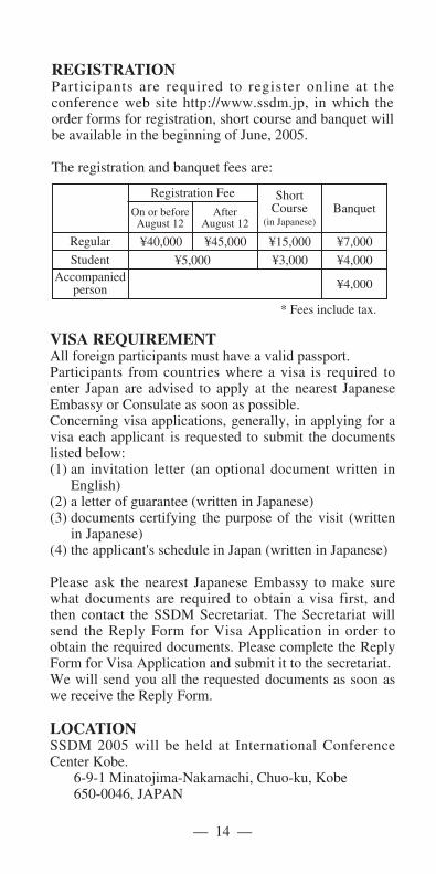
Registration Fee
On or beforeAugust 12
AfterAugust 12
BanquetShort
Course(in Japanese)
Regular ¥40,000
¥5,000
¥4,000
¥45,000 ¥15,000 ¥7,000
¥3,000 ¥4,000Student
* Fees include tax.
Accompaniedperson
— 14 —
REGISTRATIONParticipants are required to register online at theconference web site http://www.ssdm.jp, in which theorder forms for registration, short course and banquet willbe available in the beginning of June, 2005.
The registration and banquet fees are:

— 15 —
Phone: +81-78-302-5200Fax: +81-78-302-6485
International Conference Center Kobe opened in 1981.Conveniently situated on Port Island, it effectivelyfunctions as the core of Kobe’s well developedconvention facilities.A Limousine bus takes you from Kansai InternationalAirport (KIX) to Kobe in 80 minutes. InternationalConference Center Kobe is only 10 minutes from thecenter of downtown Kobe by Port Liner.For further information, see http://www.kcva.or.jp/kcc/icck/e-index.html
OFFICIAL TRAVEL AGENTJTB Corp.
Yokohama Group Tours Office6F, 3-29-1 Tsuruya-cho, Kanagawa-ku,Yokohama 221-0835, Japan
Fax: +81-45-316-5701Phone: +81-45-316-4602E-mail: [email protected]
AccommodationsJTB has blocked rooms at the following hotels in Kobefor the conference period. Reservations can be madethrough the conference website beginning in April. If thehotel of your first choice is fully booked, your secondchoice or a hotel of the same grade will be reserved.
Application and paymentParticipants wishing to reserve hotels should access theAccommodation page of the conference website. Thepage will open early in April and reservations should bemade by no later than August 19, 2005. (Confirmationsheet will be sent by JTB.)Application should be accompanied by a remittancecovering the total accommodation fee plus handling fee(¥525) due JTB.
No reservation will be confirmed in the absence of thispayment. All payment must be in Japanese yen. If theremitter's name is different from the participant's name, orif the amount covers more than one person, please informus of the details for the payment.

— 16 —
Hotel Name
Room Rates
Check-in/out
Address
Phone
Access to Hotel
To Conference site
Kobe Portopia Hotel Single: ¥9,450 Twin: ¥16,800 (per room, per night)Single Use of Twin or Double Room: ¥12,600
Check-in:13:00/Check-out:12:00
6-10-1, Minatojima Nakamachi, Chuo-ku, Kobe, 650-0046, Japan
+81-78-302-1111
2 min. walk from Port Liner Shimin-Hiroba Sta.
next to the site
Hotel Name
Room Rates
Check-in/out
Address
Phone
Access to Hotel
To Conference site
Hotel Pearl City Kobe
Single: ¥9,975 Twin: ¥17,850 (per room, per night)
Check-in:14:00/Check-out:11:00
7-5-1, Minatojima Nakamachi, Chuo-ku, Kobe, 650-0046, Japan
+81-78-303-0100
2 min. walk from Port Liner Nakafutou Sta.
5 min. walk to the site
Hotel Name
Room Rates
Check-in/out
Address
Phone
Access to Hotel
To Conference site
Quality Hotel Kobe
Single: ¥7,500 Twin: ¥17,000 (per room, per night)
Check-in:15:00/Check-out:10:00
6-1, Minatojima Nakamachi, Chuo-ku, Kobe, 650-0046, Japan
+81-78-303-5555
5 min. walk from Port Liner Shimin Hiroba Sta.
5 min. walk to the site
Hotel Name
Room Rates
Check-in/out
Address
PhoneAccess to Hotel
To Conference site
Sannomiya Terminal Hotel
Single: ¥8,820 Twin: ¥17,220 (per room, per night)
Check-in:13:00/Check-out:11:00
8-1-2, Kumoi-dori, Chuo-ku, Kobe, 651-0096, Japan
+81-78-291-0001Connecting to JR Sannomiya Sta.
15 min. by Port Liner & walk to the site
Hotel Name
Room Rates
Check-in/out
Address
Phone
Access to Hotel
To Conference site
Note: Room rates include tax and service charge. No meals are included.
Sanside Hotel
Single: ¥6,090 Twin: not availableCheck-in:15:00/Check-out:10:00
4-1-3, Kumoi-dori, Chuo-ku, Kobe, 651-0096, Japan
+81-78-232-3331
5 min. walk from JR Sannomiya Sta.
20 min. by Port Liner & walk to the site

— 17 —
Payment should be in the form of:- One of the following credit cards:
1. VISA 2. MasterCard 3. Diners Club 4. AMEX - A bank transfer to JTB Corp. (Message: SSDM)
Account at the Bank of Tokyo Mitsubishi, YokohamaBranch #480, 3-27-1 Honcho, Naka-ku, Yokohama-shi, Kanagawa 231-0005, Japan (Account number:0043079)
Cancellation policy for accommodationsIn the event of cancellation, written notification should besent to JTB. Do not contact hotels directly.The following cancellation fees will be deducted beforerefunding.Hotels: Up to 21 days before the arrival date -------------
¥5252 to 20 days before ----------------------------------
20% of daily room charge (minimum ¥525)1 day before ------------------------------------------
80% of daily room chargeOn the day of arrival or no notice given ----------
100% of daily room charge
INSURANCEThe organizer cannot accept responsibility for accidentsthat may occur during a delegate's stay. Delegates aretherefore encouraged to obtain travel insurance (medical,personal accident, and luggage) in their home countriesprior to departure.
CLIMATEKobe is warm and sometimes humid in September. Thetemperature range is 18-30˚C.
ELECTRICAL APPLIANCESJapan operates on 100 volts for electrical appliances. Thefrequency is 50 Hz in eastern Japan including Tokyo, and60 Hz in western Japan including Kyoto and Osaka.

STEERING COMMITTEE Chair: M. Morita (Osaka Univ.)Vice-Chair: T. Hiramoto (Univ. of Tokyo)Secretary: Y. Fujiwara (Osaka Univ.)Members: K. Eriguchi (Matsushita Electric)
Y. Kamakura (Osaka Univ.)S. Maekawa (Renesas)M. Nagata (Kobe Univ.)A. Sakai (Nagoya Univ.)Y. Setsuhara (Osaka Univ.)H. Tabata (Osaka Univ.)
— 18 —
Members:Y. Aoyagi (Tokyo Tech.)T. Asano (Kyusyu Inst. of Tech.)M. Fukuma (NEC)H. Hasegawa (Hokkaido Univ.)T. Hattori (Sony)S. Hiraki (Toshiba)M. Hirose (AIST)Y. Horiike (NIMS)S. Hosaka (Tokyo Electron)A. Ibaraki (Sanyo Electric)F. Ichikawa (Oki Electric)T. Ikoma (Hitotsubashi Univ.)H. Ishiwara (Tokyo Tech.)T. Kamiya (National Inst. for
Academic Degrees and Univ. Evaluation)
T. Kanayama (AIST)M. Kanazawa (ASET)A. Morino (Selete)
M. Nakamura (Hitachi)K. Natori (Univ. of Tsukuba)T. Nishimura (Renesas)M. Ogura (Matsushita Electric)T. Ohmi (Tohoku Univ.)F. Sato (NHK)Y. Shiraki (Musashi Inst. of Tech.)T. Suga (Univ. of Tokyo)K. Tada (Kanazawa Inst. of Tech.)H. Takasu (ROHM)H. Takayanagi (NTT)E. Takeda (Hitachi)M. Taneya (Sharp)K. Tsubouchi (Tohoku Univ.)H. Tsuchikawa (Fujitsu Labs.)J. Ueda (Semiconductor Industry
Res. Inst. Japan)H. Watanabe (NEC)Y. Yasuda (Kochi Univ. of Tech.)
ORGANIZING COMMITTEEChair: K. Taniguchi (Osaka Univ.)Vice-Chair: H. Sakaki (Univ. of Tokyo)
INTERNATIONAL ADVISORY COMMITTEEG. Baccarani (Univ. of Bologna)C.Y. Chang (National Chiao
Tung Univ.)C.H. Chung (Yonsei Univ.)L. Eaves (Univ. of Nottingham)L. Esaki (Shibaura Inst. of Tech.)Z.J. Li (Tsinghua Univ.)
S. Namba (Nagasaki Inst. of Applied Science)
Y. Nishi (Stanford Univ.)K.H. Ploog (Paul-Drude-Inst.)T. Sugano (Toyo Univ.)K. Takahashi (Teikyo Univ. of
Sci. & Tech.)S. Tanaka (SRL)

— 19 —
T. Takahashi (Univ. of Tokyo)Y. Uraoka (NAIST)
PROGRAM COMMITTEEChair: A. Toriumi (Univ. of Tokyo)Vice-Chair: Y. Hirayama (NTT)
K. Kim (Samsung Electronics)H. Matsuoka (Hitachi)
Secretary: T. Ichiki (Univ. of Tokyo)
Subcommittee Members:[1] Advanced Gate Stack / Si Processing ScienceChair: Y. Nara (Selete)Members: T. Aoyama (Fujitsu Labs.)
H. Hwang (Gwangju Inst. of Sci. & Tech.)S. Miyazaki (Hiroshima Univ.)B. Mizuno (UJT Lab.)A. Sakai (Nagoya Univ.)H. Satake (ASET)K. Shiraishi (Univ. of Tsukuba)Y. Tsunashima (Toshiba)R. M. Wallace (Univ. of Texas at Dallas)J. Yugami (Renesas)
[2] Characterization and Materials Engineering for Device IntegrationChair: S. Ogawa (Matsushita Electric)Members: K. Char (Seoul National Univ.)
S. C. Chen (TSMC)N. Hata (AIST)M. Kodera (Ebara)M. Matsuura (Renesas)F. Mizuno (Meisei Univ.)M. Nihei (Fujitsu Labs.)T. Tatsumi (Sony)K. Ueno (NEC)T. Yoda (Toshiba)
[3] CMOS Devices / Device PhysicsChair: K. Shibahara (Hiroshima Univ.)Members: D. Hisamoto (Hitachi)
K. Kurimoto (Matsushita Electric)H. C. Lin (National Chiao Tung Univ.)Y. Momiyama (Fujitsu)H. Oda (Renesas)M. Ogawa (Kobe Univ.)K. Ohuchi (Toshiba)

— 20 —
K. Takeuchi (NEC)J. C. S. Woo (UCLA)C. C. Wu (TSMC)
[4] Advanced Memory TechnologyChair: A. Nitayama (Toshiba)Members: I. Asano (Elpida)
T. Eshita (Fujitsu)C. Hsu (eMemory Tech.)N. Ishiwata (NEC)H. S. Jeong (Samsung Electronics)T. Kobayashi (Hitachi)Y. Ohji (Renesas)Y. Yamauchi (Sharp)
[5] Advanced Circuits and SystemsChair: H. Kobayashi (Gunma Univ.)Members: R. Fujimoto (Toshiba)
T. Hamasaki (Texas Instruments Japan)W. H. Ki (Hong Kong Univ. of Sci. & Tech.)T. Komuro (Agilent Technologies International Japan)K. Masu (Tokyo Tech.)M. Mizuno (NEC)H. Yamauchi (Sanyo Electric)
[6] Compound Semiconductor Circuits, Electron Devices and Device Physics
Chair: M. Kuzuhara (Univ. of Fukui)Members: Y.-J. Chan (National Central Univ.)
T. Enoki (NTT)T. Hashizume (Hokkaido Univ.)R. Hattori (Ion Engineering Research Inst.) S. Kuroda (Eudina Devices)K. Maezawa (Nagoya Univ.)A. Nakagawa (New Japan Radio)Y. Ohno (Univ. of Tokushima)S. Tanaka (NEC)T. Tanaka (Matsushita Electric)
[7] Photonic Devices and Device PhysicsChair: M. Sugawara (Univ. of Tokyo)Members: C. Chang-Hasnain (Univ. of California)
M. Ezaki (Toshiba)T. Hatta (Mitsubishi Electric)K. Komori (AIST)Y. Lee (Hitachi)

— 21 —
S. Noda (Kyoto Univ.)M. Tokushima (NEC)O. Wada (Kobe Univ.)
[8] Advanced Material Synthesis and Crystal Growth TechnologyChair: H. Yamaguchi (NTT)Members: H. Asahi (Osaka Univ.)
Y. Awano (Fujitsu)T. Fukui (Hokkaido Univ.)Y. Nanishi (Ritsumeikan Univ.)R. Nötzel (Eindhoven Univ. of Tech.)Y. Ochiai (NEC)S. Shimomura (Osaka Univ.)M. Tanaka (Univ. of Tokyo)K. Yamaguchi (Univ. of Electro-Communications)
[9] Physics and Applications of Novel Functional Materials and DevicesChair: Y. Takahashi (Hokkaido Univ.)Members: T. Fujisawa (NTT)
K. Ishibashi (RIKEN)K. Matsumoto (Osaka Univ.)H. Mizuta (Tokyo Tech.)J. Motohisa (Hokkaido Univ.)Y. Nakamura (NEC)Y. Ohno (Tohoku Univ.)B. G. Park (Seoul National Univ.)M. Tabe (Shizuoka Univ.)T. Usuki (Fujitsu)
[10] Organic Materials Science, Device Physics, and ApplicationsChair: K. Kudo (Chiba Univ.)Members: M. Iwamoto (Tokyo Tech.)
T. Kamata (AIST)K. Kato (Niigata Univ.)Y. Ohmori (Osaka Univ.)Y. W. Park (Seoul National Univ.)T. Sano (Sanyo Electric)A. Sugimura (Osaka Sangyo Univ.)H. Usui (Tokyo Univ. of Agri. & Tech.)
[11] Micro / Nano Electromechanical and Bio-SystemsChair: H. Tabata (Osaka Univ.)Members: S. A. Contera (Univ. of Oxford)
T. Nishimoto (Shimadzu)H. Oana (Univ. of Tokyo)T. Ono (Tohoku Univ.)

— 22 —
K. Sawada (Toyohashi Univ. of Tech.)H. Sugihara (Matsushita Electric)Y. Takamura (JAIST)Y. Yoshino (Murata Mfg.)
Persons in charge of online paper submission and registration:M. Nagata (Kobe Univ.)Y. Kamakura (Osaka Univ.)
SECRETARIAT c/o Inter Group Corp.Toranomon Takagi Bldg., 1-7-2, Nishishinbashi, Minato-ku,Tokyo 105-0003, JapanTEL: +81-3-3597-1108FAX: +81-3-3597-1097E-mail: [email protected]

— 23 —
International Conference Center Kobe
Transportation to the Venue of SSDM 2005
Airport Limousine Bus65 min.
(KATE AirportLimousine)1,800 yen
Subway 2 min.200 yen
Walk 3 min.
CAUTION
Port Liner10 min.240 yen
Kansai International Airport
Sannomiya Station
JR Tokyo Station
JR Shin-Kobe Station
INTERNATIONALCONFERENCE CENTER KOBE
A taxi from Kansai International Airport direct to International Conference Center Kobe would cost you more than 20,000 yen.
JR Shinkansen173 min.
14,670 yen
Shimin-Hiroba Station
ACCESS TO INTERNATIONAL CONFERENCE CENTER KOBE