CALIBRATION ENHANCEMENT OF NON- LINEAR …orca.cf.ac.uk/100407/1/2017AldoumaniASPhD.pdf · systems,...
192
CALIBRATION ENHANCEMENT OF NON- LINEAR VNA SYSTEM A thesis Submitted to Cardiff University in candidature for the degree of Doctor of Philosophy By Anoor Shuaib Aldoumani, BSc, MSc. Division of Electronic Engineering School of Engineering Cardiff University United Kingdom
Transcript of CALIBRATION ENHANCEMENT OF NON- LINEAR …orca.cf.ac.uk/100407/1/2017AldoumaniASPhD.pdf · systems,...

CALIBRATION
ENHANCEMENT OF NON-LINEAR VNA SYSTEM
A thesis Submitted to Cardiff University
in candidature for the degree of
Doctor of Philosophy
By
Anoor Shuaib Aldoumani, BSc, MSc.
Division of Electronic Engineering
School of Engineering
Cardiff University
United Kingdom

Anoor Aldoumani Declaration
I
DECLARATION
This work has not previously been accepted in substance for any degree and is not concurrently submitted in candidature for any degree.
Signed ……………………………………………………… (Candidate)
Date …………………………………………………………
STATEMENT 1
This thesis is being submitted in partial fulfilment of the requirements for the degree of PhD.
Signed ……………………………………………………… (Candidate)
Date …………………………………………………………
STATEMENT 2
This thesis is the result of my own independent work/investigation, except
where otherwise stated. Other sources are acknowledged by explicit
references.
Signed ……………………………………………………… (Candidate)
Date …………………………………………………………
STATEMENT 3
I hereby give consent for my thesis, if accepted, to be available for photocopying and for inter-library loan, and for the title and summary to be made available to outside organisations.
Signed ……………………………………………………… (Candidate)
Date …………………………………………………………
STATEMENT 4
I hereby give consent for my thesis, if accepted, to be available for photocopying and for inter-library loans after expiry of a bar on access approved by the Graduate Development Committee.
Signed ……………………………………………………… (Candidate)
Date …………………………………………………………

Anoor Aldoumani Acknowledgements
II
ACKNOWLEDGEMENTS
First and foremost I would like to thank my supervisors Prof. Paul Tasker and Dr Jonny
Lees for their inspiration, support and guidance throughout the duration of the PhD, and
for giving me the opportunity to study for this degree, albeit in rather unique
circumstances.
I’d like to thank my industrial supervisor; Dr. Tudor Williams for his involvement, help
and supervision in the initial stages of my PhD, and for knowing exactly how to deal
with just about any problem. The enthusiasm and commitment in the lab to high quality
research is infectious and inspiring.
I would like to thank Engineering and Physical Sciences Research Council (EPSRC),
Mesuro Ltd and Cardiff University for sponsoring this work and for the technical
support during the course of the PhD, and preparation of the thesis.
I would also like to thank other academics of Cardiff University, especially Dr Richard
Perks and Prof Adrian Porch.
I owe a debt of gratitude to my parents and my family who have always encouraged me
to do my best in life.
I would like to thank colleagues and friends that I had the pleasure to work with at the
Centre for High Frequency Engineering at Cardiff University. Dr Friday Lawrence
Ogboi, Dr James Bell, David Loescher, Zulhazmi Mokhti, Syalwani Kamarudin,
Minghao Koh, Dr. Akmal Chaudhry, Dr R. Saini and Dr Timothy Canning.

Anoor Aldoumani Abstract
III
ABSTRACT
Communication systems are generally found wherever data is to be transmitted from
point-to-point or from a point to many points. It is impossible to imagine modern life
without communication systems such as radio, telephone, TV, Satellite and etc.
The transmission of information from one place to another requires an operation or
other alteration to be sent through an electrical signal; the same principle applies for the
receiving terminal.
Modern life requires that efficient wireless communication systems for long range
transmission be built, therefore, base-stations must use high power transistors almost
exclusively. Furthermore, modern cellular communication systems also need to transmit
across long distances, hence, to achieve this aim successfully, a radio frequency (RF)
power amplifier is employed. That is considered to be a key element of any wireless
communication system. Efficient communication systems must have minimum spectral
re-growth, interference and employ linear.
Signal amplification is one of the core circuit functions in modern microwave and RF
systems. The Power Amplifier (PA) is a key element in the construction of all wireless
communication systems. The PA uses the most current because it is the last stage in the
transmission chain.
In modern PA design, the RFPA designer must have accurate S-parameter data for the
DUT, thereby allowing the creation of an accurate system model and to reduce the re-
design and rework effort. The ultimate aim of the research work presented in this thesis
is to achieve improvement in the accuracy of a waveform measurement system by
increasing the accuracy of the small-signal calibration used. This involved removing the
phase reference from the NVNA during calibration and operation, which in turn
removes the bandwidth and frequency limitations that the phase reference imposes, as
well as reducing the complexity of the overall system.
Essential contributions to this research work concentrated in two areas; firstly,
developments that allow for Enhanced Vector Calibration of Load-pull measurement
systems, especially near the edge of the Smith Chart, and secondly, the operation and

Anoor Aldoumani Abstract
IV
calibration of a VNA-based large-signal RF I-V waveform measurement system without
using a harmonic phase reference standard.
The first research area described in this thesis involved investigating the prospect of
improving vector measurement accuracy, especially near the edge of the Smith Chart,
by using load pull technology. Increased measurement error near the edge of the Smith
chart was observed during calibration. To help correct this, the realisation of novel
optimization that increases the accuracy of all the raw data which was collected during
calibration process and therefore increases the accuracy of calibration at reflection
coefficients close to unity. This research work focuses on taking advantage of the load-
pull capability during calibration, this reduces the effect of measurement errors on the
raw data when measuring the calibration standards before being applied in traditional
LRL/TRL calibration algorithms. Leading to time proved measurement accuracy and
eliminates the requirement to use complex optimisation algorithms post calibration.
The second concept developed simplifies the NVNA architecture and removes the
complexities and bandwidth limitations introduced when employing a harmonic phase
reference generator. A key capability of the Rohde and Schwarz ZVA-67 VNA is that it
incorporates internal signal and local oscillator sources and employs direct digital
synthesis was exploited to advantage allows the Vector Network Analyzer to be
operated as a NVNA without the need for a harmonic phase reference generator. This is
due to such a Vector Network Analyzer based NVNA configuration provided a system
with both coherent receivers and sources. This feature combined with a modified
calibration procedure, means that during calibration only the internal signal sources and
an external phase meter are required during measurement. All the internal signal sources
and receiver port are available to measure, also now since no phase reference required,
bandwidth and functionality issues and avoided.

Anoor Aldoumani List Of Publications
V
LIST OF PUBLICATION
First-author papers
1- A. Aldoumani, P. J. Tasker, R. S. Saini, J. W. Bell, T. Williams and J. Lees, "Operation and calibration of VNA-based large signal RF I-V waveform measurements system without using a harmonic phase reference standard," Microwave Measurement Conference (ARFTG), 2013 81st ARFTG, Seattle, WA, 2013, pp. 1-4.doi: 10.1109/ARFTG.2013.6579055. URL:http://ieeexplore.ieee.org/stamp/stamp.jsp?tp=&arnumber=6579055&isnumber=6579016
2- A. Aldoumani, T. Williams, J. Lees and P. J. Tasker, "Enhanced vector calibration of load-pull measurement systems," Microwave Measurement Conference (ARFTG), 2014 83rd ARFTG, Tampa, FL, 2014, pp. 1-4. doi: 10.1109/ARFTG.2014.6899508. URL:http://ieeexplore.ieee.org/stamp/stamp.jsp?tp=&arnumber=6899508&isnumber=6899500
Additional papers
1- N. Aldoumani, T. Meydan, C. M. Dillingham and J. T. Erichsen, "Enhanced tracking system based on micro inertial measurements unit to track sensorimotor responses in pigeons," SENSORS, 2015 IEEE, Busan, 2015, pp. 1-4.doi: 10.1109/ICSENS.2015.7370309 URL: http://ieeexplore.ieee.org/stamp/stamp.jsp?tp=&arnumber=7370309&isnumber=7370096
End

Anoor Aldoumani Content
VI
TABLE CONTENTS
CONTENTS DECLARATION ............................................................................................................... I
Acknowledgements .......................................................................................................... II
Abstract ........................................................................................................................... III
List of publication ............................................................................................................ V
Table Contents ................................................................................................................ VI
Abbreviations .................................................................................................................. IX
1. Chapter 1 .............................................................................................................. 12
1.1 Background ...................................................................................................... 12
1.2 Motivation ........................................................................................................ 15
1.3 Objectives and Structure of The Thesis ........................................................... 18
1.4 Chapter Synopsis .............................................................................................. 19
1.5 Reference .......................................................................................................... 20
2. Chapter 2 .............................................................................................................. 22
2.1 Introduction ...................................................................................................... 22
2.2 RF Waveform Measurement ............................................................................ 22
2.2.1 DC Measurement ...................................................................................... 24
2.2.2 RF Measurements(S-Parameter) ............................................................... 24
2.2.2.1 Sources and Types of Errors .............................................................. 28
2.2.2.2 Small Signal Calibration .................................................................... 29
2.2.2.3 Error Model for VNA ........................................................................ 32
2.3 Calibration Methods ......................................................................................... 41
2.3.1 Short-Open-Load-Thru (SOLT) ................................................................ 44
2.3.1.1 Open Standards .................................................................................. 47
2.3.1.2 Short standards ................................................................................... 47
2.3.1.3 Load Standard .................................................................................... 48
2.3.1.4 Calibration Producer .......................................................................... 48
2.3.2 Line-Reflect-Line (LRL), (TRL) and (TRM) ........................................... 53
2.3.2.1 Thru- Line- Reflect (TRL) ................................................................. 54
2.3.2.2 Thru Standard .................................................................................... 56

Anoor Aldoumani Abstract
VII
2.3.2.3 Line Standard ..................................................................................... 58
2.3.2.4 Reflection Standard............................................................................ 61
2.4 Uncertainty calibration ..................................................................................... 69
2.4.1 Uncertainty in Reflection .......................................................................... 69
2.4.2 Uncertainty in Source Power .................................................................... 70
2.4.3 Uncertainty in Power Meter ...................................................................... 70
2.4.4 Uncertainty in Transmission ..................................................................... 71
2.5 Conclusions ...................................................................................................... 72
2.6 Reference .......................................................................................................... 73
3. Chapter 3 .............................................................................................................. 77
3.1 Calibration TRL ............................................................................................... 77
3.2 Introduction to Enhanced Calibration .............................................................. 77
3.2.1 Traditional calibration ............................................................................... 78
3.2.2 Validity of Traditional calibration ............................................................ 90
3.2.3 Enhanced Calibration (New Method) ....................................................... 98
3.3 Quality of Raw Data affects in Calibration Accuracy .................................... 115
3.4 Relation between 𝜞𝒍𝒐𝒂𝒅and accuracy ........................................................... 115
3.5 Summary ........................................................................................................ 123
3.6 Reference ........................................................................................................ 124
4. Chapter 4 ............................................................................................................ 126
4.1 Introduction .................................................................................................... 126
4.2 Nonlinear Measurement system ..................................................................... 127
4.2.1 Types of LSNA ....................................................................................... 129
4.2.1.1 Sampling-based (Oscilloscopes) ...................................................... 129
4.2.1.1.1 Calibration (Oscilloscopes).............................................................. 130
4.2.1.2 Sub-sampling-based ......................................................................... 131
4.2.1.2.1 Microwave Transition Analyser (MTA) ....................................... 133
4.2.1.2.2 Calibration .................................................................................... 134
4.2.1.3 Mix-Mixer-based ............................................................................. 136
4.2.1.3.1 Calibration .................................................................................... 139
4.3 Summery Nonlinear ....................................................................................... 142
4.4 Reference ........................................................................................................ 143
5 Chapter 5 ............................................................................................................ 147

Anoor Aldoumani Abstract
VIII
5.1 Introduction .................................................................................................... 147
5.2 Motivation ...................................................................................................... 148
5.3 Phase Coherence ............................................................................................. 149
5.4 Direct Digital Synthesis .................................................................................. 150
5.5 Operation VNA without Phase Reference ...................................................... 152
5.5.1 Phase Coherence of VNA (ZVA-67) ...................................................... 156
5.5.1.1 Phase reference trigger..................................................................... 156
5.5.1.2 Receiver ........................................................................................... 161
5.5.1.4 Phase Calibration ............................................................................. 171
5.5.2 Calibration ............................................................................................... 172
5.5.3 Calibration Validation ............................................................................. 177
5.6 Summary ........................................................................................................ 185
5.7 Reference ........................................................................................................ 186
6 Chapter 6 ............................................................................................................ 188
6.1 Conclusions .................................................................................................... 188
6.2 Future Work ................................................................................................... 190
6.3 Reference ........................................................................................................ 191
End Contai

Anoor Aldoumani Abbreviations
IX
ABBREVIATIONS
A Amperes
AC Alternate Current
ADC Analog to Digital Converter
ADS Advanced Design System
ALG Algorithm
𝐴𝑛 Incident voltage travelling wave, where n is the port number
ARFTG Automatic Radio Frequency Techniques Group
𝐵𝑛 Voltage travelling wave, where n is the port number
BW Bandwidth
C Capacitance
CAD Computer-Aided Design
CW Continuous Wave
dB Decibels
𝑑𝐵𝑚 Decibels (reference to 1mW)
DC Direct Current
DCIV DC measurement of the device’s output current/voltage plane
DSO Digital Sampling Oscilloscope
DE Drain Efficiency
DSP Digital Signal Processing
DUT Device Under Test
ESG Electronic Signal Generator
F Farads
FEC Forward Error Correction

Anoor Aldoumani Abstract
X
FET Field Effect Transistor
FFT Fast Fourier Transform
𝑓0 Fundamental Tone of a signal
Hz Hertz
I Current
𝐼𝐷𝐶 DC drain bias current
IF Intermediate Frequency
IFFT Inverse Fast Fourier Transform
I-V Current-Voltage
L Inductance
LSNA Large Signal Network Analyser
m Meter
MTA Microwave Transition Analyser
NVNA Non-Linear Vector Network Analyser
P Power
PA Power Amplifier
R Resistance
RF Radio Frequency
RFPA Radio Frequency Power Amplifier
S-parameters Scattering Parameters
𝑡 Time
V Voltage
𝑉𝐷𝐶 DC drain bias voltage
𝑉𝐷𝑆 Drain-Source Voltage
𝑉𝐺𝐷 Gate-Drain Voltage
𝑉𝐺𝑆 Gate-Source Voltage

Anoor Aldoumani Abstract
XI
VNA Vector Network Analyser
VSA Vector Signal Analyser
W Watts
X Reactance
Z Impedance
𝑍𝑙𝑜𝑎𝑑 Load Impedance
Г Reflection Coefficient
Ω Ohm, unit of Impedance
η Efficiency
λ Wavelength
π Pi
ω Radian Frequency, ω =2 π f
∞ Infinity
| | Magnitude
˂ Angle
Degree
End Abber

Anoor Aldoumani Chapter 1
12
1. CHAPTER 1
INTRODUCTION
1.1 BACKGROUND
The reason behind the consideration of RFPA as a key element is due to the presence of
a trade-off between power per cost vs. efficiency and linearity [1].
Digital communication requires more peak power for the same bit error rate,
transmitters must be more linear to minimise spectral re-growth, interferences, higher
power and broader bandwidth to clear modulation scheme. There are two behaviour
regions for the operation of PA, linear and non-linear [1].
Devices are considered to be a linear response only if the number of harmonics in input
equals the numbers of harmonics in output, whereas non-linear devices generate more
harmonics in the output. Many components that exhibit linear behaviour in normal
cases, if driven with large enough input signal, will exhibit non-linear behaviour [2].
RFPA designers require information in order to make correct decisions throughout all
stages of the design process, They need to be informed on stability analysis, DC
network analysis, harmonic balanced analysis, convolution analysis, transient analysis,
3D EM analysis, modulation envelop analysis, smith tool utility and load pull analysis.
Normally, PA designers start designing in the linear region depending on S-parameter.
This provides insight into the characteristics of behaviour of the linear two-port device,
𝑆21 =forward transmission coefficient (gain or loss), 𝑆12 =reverse transmission
coefficient (isolation), S21=forward reflection coefficient (input match), S22=reverse
reflection coefficient (output match) [2].

Anoor Aldoumani Chapter 1
13
𝒃𝟏𝒃𝟐 = 𝑺𝟏𝟏 𝑺𝟏𝟐
𝑺𝟐𝟏 𝑺𝟐𝟐 .
𝒂𝟏𝒂𝟐 EQUATION 1-1
Measurement: Within the context of this thesis, measurement involves applying a
sequence of stimuli to the DUT and measuring its response to these stimuli. During this
process, the order of the various tests must be considered, along with other testing
conditions and other aspects of the stimulus [3]. RF measurement can be considered in
two general groups, with sometimes overlapping categories:-
1. Signal Measurements:-“observation and determination of the absolute
characteristics of waves and waveforms. This includes frequency and time
characteristics that are intentionally imparted into or onto a signal such as
modulation by information or unintentional signal perturbations including phase
and amplitude noise”[4].
2. Network Measurements: “determines the relative terminal and signal transfer
characteristics of devices and systems with any number of ports. Networks such
as modulators and communication paths are sometimes characterized as linear
time variant paths requiring both signal and network measurements for
characterization”[4].
In RFPA design, a first-pass methodology and elimination of the need for post-
production tuning requirements and rework is desirable. If there is an absence of reliable
non-linear models, this goal can only be fully accomplished by undertaking all relevant
measurements of the device to be used in the RFPA design. As a result, continuous
waveform measurements are considered a very important step in the RFPA design
procedure, especially for nonlinear devices and circuits [5].
All new systems are built based on these aforementioned measurement requirements.
To further expand the boundaries future systems are pushing towards multi-tone
excitation. The driving factors are a demand for faster CW device characterisation and
the ability to build measurement systems that can perform ultra-rapid CW
characterisation. These enhanced measurement systems allow the users to more rapidly
generate models and in turn provide faster time-to-market for products [6].
AS the nonlinear measurements are used to generate a model for DUT, the precision of
these models is clearly dependent on the density of measured information. This density

Anoor Aldoumani Chapter 1
14
can be dramatically increased by using a modulated impedance environment and
modulated stimuli. The second demand comes from the dramatic growth in the
complexity of modulation schemes, predominantly operating over wide bandwidths [7].
The relationship between traditional CW measurements and the eventual simulation the
device or circuit encounters in the final application is a concern. To address these
problems, further measurements need to be performed under more simulation stimuli,
allowing the performance of the device in the measurement system to be directly linked
to the final application [6-8].
b3RAW a3RAwa0RAW b0RAW
DUTPort 2CouplerPort 1Coupler
Microwave Source Trigger
Port 2Port 1
Non-Linear Network analyser
RCVR
Switch
a1RAW a2RAW
b1RAW b2RAW
RCVR RCVRRCVR
DCinput
DCinput
FIGURE 1-1 NON LINEAR NETWORK ANALYSER.

Anoor Aldoumani Chapter 1
15
1.2 MOTIVATION
According to recent market research [5], firm insight research Corp, the total revenue
for telecommunications industry for 2015 is set to reach $2.1 trillion and expected
industry revenue will grow up at an average annual rate of 5.3% to $2.7 trillion in 2017.
Growing revenue combined with a requirement for new end products that not only
provide added functionality, but also offer continually improving performance, poses
major challenges, pushing the industry to evolve and change. The demand for high
spectral efficiency and high data rates inevitably results in new modulation schemes and
increased design complexity. In order to meet these growing requirements for
performance a more flexible, faster and accurate design and realisation approach for RF
devices, circuits and systems is required [7]. Generating, testing and validation of robust
computer aided design (CAD) models opens the door to design, test and optimisation of
devices and circuits being linked within simulation environments [8].
Appropriate measurement data should be used to generate CAD models. The use of
CAD tools is becoming fundamental in PA design to obtaining 1st pass design success,
but this depends heavily on the accuracy of the models for the DUT. A non-accurate
measurement system, leads to a poor model which means at the simulation stage the
design is not optimised correctly. This will give unsatisfactory results increased design
costs and fabrication processes, moreover leading to increased time expenditure. This in
turn means the accurate extraction and validation for DUT models is an important factor
that determines the success of the design [9- 11].
For linear design, the desired measurement data are S-parameters. S-parameter
measurements are carried out under small signal conditions by using vector network
analysis (VNA) as shown below in Figure 1-2.

Anoor Aldoumani Chapter 1
16
4-Channel Receiver
a0Raw b0Raw
a1Corr
b1Corr
a2Corr
b2Corr
b3Raw a3Raw
DUT
FIGURE 1-2 A GENERIC TWO PORT LSNA RF ARCHITECTURE WITH INTEGRATED ACTIVE LOAD-PULL.
Only the perfect instrument would not need correction, however measurement
instruments have imperfections and thereby do not provide the ideal measurement
required by PA designers. Therefore all measurement results include some measurement
uncertainty. The sources of uncertainty (error in VNA measurements) are essentially the
result of systematic, random, and drift errors. Systematic error can be removed by using
the equation 1-2 which is representing the general calibration formula. Random and
drift measurement errors vary randomly as a function of time, this type of error, cannot
be completely removed but random errors could be reduced by averaging, and drift
errors limited by controlling the environment [11, 12].
𝒃𝟏𝒂𝟏𝒃𝟐𝒂𝟐
=
⎣⎢⎢⎢⎢⎢⎡
𝟏𝒆𝟎𝟏𝒆𝟏𝟎
−𝒆𝟎𝟎𝒆𝟎𝟏𝒆𝟏𝟎
𝒆𝟏𝟏𝒆𝟎𝟏𝒆𝟏𝟎
(𝒆𝟎𝟏𝒆𝟏𝟎−𝒆𝟎𝟎𝒆𝟏𝟏)𝒆𝟏𝟎𝒆𝟎𝟏
𝟎 𝟎𝟎 𝟎
𝟎 𝟎𝟎 𝟎
𝟏𝒆𝟑𝟐𝒆𝟏𝟎
− 𝒆𝟑𝟑𝒆𝟑𝟐𝒆𝟏𝟎
𝒆𝟐𝟐𝒆𝟑𝟐𝒆𝟏𝟎
(𝒆𝟑𝟐𝒆𝟐𝟑−𝒆𝟑𝟑𝒆𝟐𝟐)𝒆𝟑𝟐𝒆𝟏𝟎 ⎦
⎥⎥⎥⎥⎥⎤
.
𝒃𝟎𝒂𝟎𝒃𝟑𝒂𝟑
EQUATION 1-2
Spectrum analysers, power meters, oscilloscopes and vector network analyzer (VNA)
are used to acquire and analyse RF signals. Operating the transistor nearer to its
compression region is due to increased demand for enhanced performance from the
transistor devices [13].

Anoor Aldoumani Chapter 1
17
Nonlinear vector network analyzer (NVNA) is an instrument that depends on VNA
measurements with extended capabilities. It must be used with large signal RF
measurements to truly characterise the nonlinear devices. A historical overview of the
development of the LSNA, by M. Sipila was published in 1988 a first prototype of a
LSNA, The aim was to build a measurement system that could perform accurate
measurement of the voltage and current waveforms at the gate and drain of a HF
transistor. The measurements are performed in the time domain using a broadband
sampling oscilloscope and Fourier transforms into the frequency domain. After error
correction, the results are transformed back into the time domain [14].
All previous measurement systems have the ability to observe and quantify the time
varying voltage 𝑉𝑛(𝑡)and current 𝐼𝑛(𝑡) present at all terminals of the Device Under Test
(DUT): thus involves all frequencies including DC, IF and RF because this type of
measurement system has fixed impedance which is lead for a limited insight into the
non-linear behaviour of semiconductor devices [15].
The PA designers require more information about the DUT to improve power amplifier
efficiency. It is worth mentioning that significant design effort is devoted to developing
microwave transistors and high-performance RF thereby an accurate and repeatable
characterisation tool is required to estimate the performance of the transistor for this
“Waveform-Engineering” necessary to obtain these aims [16].
Waveform-engineering is defined as: The ability to modify in a quantified manner the
time varying voltage 𝑉𝑛(𝑡)and current 𝐼𝑛(𝑡)present at the terminals of the Device under
Test (DUT): thus involves all frequencies including DC, IF and RF [16, 17].
The waveform engineering technique is suitable for use in the investigation, design and
evaluation loop of RF power amplifiers. Use of the waveform engineering technique in
RF power amplifier design facilitates an intelligent new design process and eliminates
the black box design process [18].
Theoretical waveform analysis supports power amplifier design by improving
computer-aided design (CAD) accessible behavioural or the accuracy of nonlinear
transistor models or behavioural model parameter datasets [18].

Anoor Aldoumani Chapter 1
18
1.3 OBJECTIVES AND STRUCTURE OF THE THESIS
The research work present in this thesis focuses on improving the calibration of a non-
linear RF measurements system and so increases the capability and accuracy of such
measurements systems.
The main objective of this thesis is to advance the operation and calibration of VNA-
based large signal RF I-V waveform measurements systems. Targeting the elimination
of the harmonic phase reference standard and improving the vector measurement
accuracy, especially near the edge of the smith chart, is very important in load-pull
measurement systems. The ultimate aim for improving the operation and calibration of
emerging VNA based NVNA measurement systems is to reduce restrictions on the
frequency grid and bandwidth. Importantly, as no dedicated channel is required for
triggering during waveform measurements, all four VNA ports are available for DUT
characterisation, eliminating the need for multiplexing measurement signals, and
allowing a simple and rapid measurement approach.

Anoor Aldoumani Chapter 1
19
1.4 CHAPTER SYNOPSIS
Chapter 2: presents a literature review of the waveform measurement techniques that
have been employed starting from DC to RF. Specifically mentioned and discussed are:
S-parameters, error models, small signal calibration and large signal calibration. Two-
port calibration techniques are also discussed in detail.
Chapter 3: shows the enhancement calibration that can be achieved by varying the
output reflection coefficient around a Smith chart by using a Load-pull system in
combination with a TRL calibration technique. Also described is the use of the load pull
system with TRL calibration algorithm to achieve more accurate calibration results. The
quality of raw data collected during calibration process and its effect on calibration
accuracy is discussed, as well as changes to the reflection coefficient and its impact on
the quality of raw data.
Chapter 4: contains a review of the various Nonlinear Measurement systems in use
today, including sample-based and mixer based approaches. Also presented is an
overview of the different architectures of several Non-linear measurement systems and
calibration techniques that are used to make these measurements is acceptable.
Chapter 5: investigates a new approach that allows a Vector Network Analyzer to be
operated as a Large Signal Network Analyzer without the need for a harmonic phase
reference generator. Extensive verification shows how certain VNAs have coherent
sources. Investigations of calibration and operation of VNAs based on LSNAs are now
possible through the use of a phase meter to calibrate the measured phase of the VNA
during the calibration process and allow to alignment and to improve bandwidth and
thus improve measurement system utilisation efficiency.
Chapter 6: is a conclusion to the thesis that presents a discussions on future developments of the measurement system that can benefit from this work.

Anoor Aldoumani Chapter 1
20
1.5 REFERENCE
1- White, J.F., High Frequency Techniques: An Introduction to RF and
Microwave Engineering. 2003: Wiley.
2- González, G., Microwave transistor amplifiers: analysis and design.
1984: Prentice-Hall.
3- Dunsmore, J.P., Handbook of Microwave Component
Measurements: with Advanced VNA Techniques. 2012: Wiley.
4- Golio, M. and J. Golio, RF and Microwave Circuits, Measurements,
and Modeling. 2007: Taylor & Francis.
5- Cripps, S.C., RF Power Amplifiers for Wireless Communications.
2006: Artech House.
6- McGenn, W., RF IV Waveform Engineering Applied to VSWR
Sweeps and RF Stress Testing. 2013.
7- Epstein, Z. Global telecommunications industry revenue to reach
$2.1 trillion in 2012. 2012 [cited 2014 1/12]; Available from:
http://bgr.com/2012/01/05/global-telecommunications-industry-
revenue-to-reach-2-1-trillion-in-2012/.
8- Collin, R.E., Foundations for Microwave Engineering. 2001: Wiley.
9- Golio, M. and J. Golio, RF and Microwave Passive and Active
Technologies. 2007: Taylor & Francis.
10- Agilent, Network Analyzer Basics. 2010, Agilent Technologies.
11- Agilent. S-Parameter Design Application Note Agilent AN 154.
USA.
12- Sasaoka, H., Mobile Communications. 2000: Ohmsha Limited.
13- Agilent, AN 1287-3 Applying Error Correction to Network
Analyzer Measurements. 2002.

Anoor Aldoumani Chapter 1
21
14- Sipila, M., K. Lehtinen, and V. Porra, High-frequency periodic
time-domain waveform measurement system. Microwave Theory
and Techniques, IEEE Transactions on, 1988. 36(10): p. 1397-1405.
15- Tasker, P.J., Practical waveform engineering. Microwave
Magazine, IEEE, 2009. 10(7): p. 65-76.
16- Tasker, P.J. RF Waveform Measurement and Engineering. in
Compound Semiconductor Integrated Circuit Symposium, 2009.
CISC 2009. Annual IEEE. 2009.
17- Tasker, P.J., et al. Wideband PA Design: The "Continuous" Mode
of Operation. in Compound Semiconductor Integrated Circuit
Symposium (CSICS), 2012 IEEE. 2012.
18- El-deeb, W.S., et al., Small-signal, complex distortion and
waveform measurement system for multiport microwave devices.
Instrumentation & Measurement Magazine, IEEE, 2011. 14(3): p.
28-33. chapter1

Anoor Aldoumani Chapter 2
22
2. CHAPTER 2
CALIBRATION AND OPERATION OF A NON-LINEAR MEASUREMENT SYSTEM:
LINEAR CALIBRATION
1.6 INTRODUCTION
The literature review of existing linear RF measurement systems, architectures and
calibration methods used to calibrate the measurements systems. The different
measurement architectures will be discussed along with the advantages and the high-
lighting the problems of each of the measurement techniques.
1.7 RF WAVEFORM MEASUREMENT
Waveform measurement can be defined as “the ability to observe and quantify the time
varying voltage 𝑉𝑛(𝑡) and current 𝐼𝑛(𝑡) present at all terminals of a device under test
(DUT): this involves all frequencies including DC, IF and RF”[1]. In general the
frequency domain is normal for standard microwave measurement tools. For more than
30 years, the vector network analyzer (VNA) has been a key-tool in any RF and
microwave laboratory, specifically for measuring the S-parameters of a system [2].

Anoor Aldoumani Chapter 2
23
FIGURE 2-1WAVEFORM ENGINEERING.
The technique that is used to measure current and voltage (I-V) waveforms depends
largely upon the relation between the length of the conductor and the wavelength of the
signal. For example, a normal wire is used as a probe at low frequencies (when the
length of the cables in the system are much smaller than the wavelength of the signals).
At high frequencies (in practice, all frequencies higher than 10MHz are considered to be
a high frequency) a different technique needs to be implemented to measure I-V
waveforms. This technique is implemented because the length of conductors involved in
the system is much larger than the wavelength of signals and the impossibility to control
low or high impedances across the entire bandwidth, ruling out the use of simple current
and voltage probes [3].
This will lead to connection mismatch problems among the DUT, signal source, and
data acquisition samplers, therefore a transmission line is necessary for efficient power
transmission. There are many obstacles in measuring high-frequency I-V waveforms.
The main issue arises from common technological limitations that are generic at high
frequencies. From the above problem, we can understand the inability of standard
oscilloscopes to measure all the harmonic components, because of the restriction in
bandwidth of the scopes. Obtaining I-V waveforms at high frequencies, can be achieved
by measuring the incident, reflected and transmitted travelling waves travelling along
the transmission line [2, 3]. The incident (𝑎𝑛ℎ) and reflected (𝑏𝑛ℎ) components at the
terminals of the DUT consist of fundamental and harmonic waves. These can then be
used to calculate the periodic current and voltage waveforms at the terminals of the
device, where h refers to the harmonic number and n the DUT port number [4].

Anoor Aldoumani Chapter 2
24
1.7.1 DC MEASUREMENT
DC measurement is considered to be an important initial step used by both RFPA
designers and device manufacturers. There are many different methods to characterise
the DC electrical properties of an RF transistor, but all typically involve varying input
and output bias voltages, and observing the resultant drain current. This data is then
plotted as output current vs. input voltage, and output current vs. output voltage, output
characteristics [5].
FIGURE 2-2 DCIV MEASUREMENT OF AN FET DEVICE.
1.7.2 RF MEASUREMENTS(S-PARAMETER)
Scattering- (or S-) parameters are important in microwave design, and are considered as
the mathematical regime for representing linear networks at higher frequencies, being
considered the optimal tool for simulation and design since the 1960s. S-parameters
describe the magnitude and phase relationships between incident and reflected travelling
waves, and as result are able to accurately characterise and analyse the electrical
behaviour of linear time invariant systems. S-parameters are based on the super position
principle, and therefore, can be used only with linear systems. S-parameters have many

Anoor Aldoumani Chapter 2
25
advantages over other parameters which is related to familiar measurements (gain, loss,
reflection coefficient etc) [5].
S-parameters represent the ratios between incident ( 𝑎(𝑓)𝑛) and reflect ( 𝑏(𝑓)𝑛 )
travelling waves for each port(n) as a function of frequency(f), which are related to a
constant measurement impedance environment of 50Ω, as shown in equation 2-1.
Where (j) refers to the receiver port and (i) refers to sender port [5].
𝑺(𝒇)𝒋𝒊 = 𝒃(𝒇)𝒋𝒂(𝒇)𝒊
EQUATION 2-1
DUT
Signal Separation
Receiver/Detector
Processor/Display
Incident Wave Reflected Wave Reflected Wave Incident Wave
a1 b1 a2 b2
RF Test Set
RF Section
Digital Section
Reference plane
Port 1 Port 2
FIGURE 2-3 SIMPLIFIED BLOCK SCHEMATIC OF TWO-PORT VNA.
𝑁2 An N-port device is defined by 𝑁2 S-parameters represent. By using equation 2-1,
can lead to obtain equation 2-2 to represent the network which consists of N-ports in an
S-parameter matrix.
𝒃𝟏⋮𝒃𝒏 =
𝑺𝟏𝟏 ⋯ 𝑺𝟏𝒎⋮ ⋱ ⋮𝑺𝒏𝟏 ⋯ 𝑺𝒏𝒎
∙ 𝒂𝟏⋮𝒂𝒎
EQUATION 2-2

Anoor Aldoumani Chapter 2
26
The periodic voltage and current waveforms at higher frequencies can be calculated at
the terminal of device under test from the measured travelling waves as shown in
equation 2-3 and 2-4. The periodic voltage and current waveforms consist of
fundamental and harmonic waves (𝑎𝑛𝑖 ) and (𝑏𝑛𝑖 ), where (𝑛) represent the number of
ports and (𝑖)represent harmonic number.
𝑽𝒏(𝒊) = 𝒁𝒐𝒂𝒏
(𝒊) + 𝒃𝒏(𝒊) EQUATION 2-3
𝑰𝒏(𝒊) = 𝟏/𝒁𝒐𝒂𝒏
(𝒊) − 𝒃𝒏(𝒊) EQUATION 2-4
Where 𝑍𝑜is 50 Ω for all harmonics, 𝑽𝒏(𝒊) and 𝑰𝒏
(𝒊) are the (i)th Fourier coefficients [3,6].
S-parameter data describes the behaviour of a device under test when undergoing
various situations. This is achieved by measuring the incident and reflected travelling
waves at the input and output of DUT. Determination of S-parameters is the principle
measurement capability of vector network analyzers (VNA). Characterisation of most
types of microwave components is carried out using a classic vector network analyzer
(VNA) to measure the S-parameters. S-parameter data obtained from the measurement
stage can be imported directly into the designers CAD environment, where the
simulated device behaviour precisely copies the measured device behaviour. Highly
efficient design can be achieved, by using VNA to provide a consistency check between
the mathematical abstraction that resides inside the simulator and the actual physical
device [7, 8].
Vector network analyzers (VNA) are an essential tool in measuring and characterising
power amplifiers (PAs), components and circuits. A VNA is usually applied to measure
small signal or linear characteristics of multi-port networks, at frequencies ranging from
RF to beyond 100 GHz, it compares the incident wave to reflected wave. The S-
parameter for represent the relationship between scattered waves (𝑎, 𝑏) and the S-
parameter values will be complex liner power quantities. The definitions of the S-
parameter for two port device are shown in Equation 2-5 [8].

Anoor Aldoumani Chapter 2
27
b1
b2
=S11 S12
S21 S22
.a1
a2
Reflection Waves
Incident Waves
Port where measurement in
made
Port where Stimulus in made
EQUATION 2-5
ABOVE DIAGRAM STIMULS IS MADE NOT IN MADE
The S-parameter terms for the two-port device will be:-
𝑆11= Forward reflection coefficient (input match),
𝑆22= Reverse reflection coefficient (output match).
𝑆21= Forward transmission coefficient (gain or loss).
𝑆12= Reverse transmission coefficient (isolation).
The VNA can perform many types of measurements such as reflection coefficients (𝑆11,
𝑆22), Impedance (r+jx), Return loss (dB),Reflection coefficients vs. Distance (Fourier
Transform), VSWR, gain (dB), insertion phase (degrees) and insertion loss (dB) usually
used to measure small signal or linear characteristics of multi-port networks. The VNA
architecture is limited for waveform engineering because the VNA is capable of
measuring only a single frequency at a time. As result the VNA is not able to measure
relative phase between different frequency components. Additionally, typical VNA
measurements ignore non-linear effects due to memory effects and distortions generated
by mixing. This means the systems are able to capture S-parameter with linear analysis
because S-parameter uses the superposition principle therefore this type of system has
no ability to measure, for example, energy transfer from the stimulus to other harmonic
frequencies. This leads to the conclusion that the data obtained from this system has
limitations for use in large signal device models [9].

Anoor Aldoumani Chapter 2
28
A VNA made to precisely characterize the behaviour of a DUT by measuring the
magnitude and phase of reflected (b) and incident (a) waves. By measuring the waves,
VNA is able to give the characteristics of a DUT. The increased accuracy has lead to
improvements in the design of RFPA. The cost involved prohibits the development of
perfect VNA hardware that is perfect, in the sense that the need for error correction is
totally eliminated.
Vector error correction is an effective method for obtaining improved in performance of
system measurement. The relation between VNA hardware performance, system
performance and cost, should be balanced across these elements. Vector error correction
cannot amend errors due to poor VNA performance, on other hand good VNA that will
not make up for inherent calibration in accuracies. Calibrating the VNA will lead to the
eliminate the largest contributor to measurement uncertainty systematic errors [2, 9].
2.2.2.1 SOURCES AND TYPES OF ERRORS
It is useful for the designer to have accurate S-parameters of the DUT, thereby allowing
creation of accurate system models for reduce design effort and rework. Only the
perfect instrument would not need correction. Measurement instruments have
imperfections, thereby leading to less than ideal measurements that are required by PA
designers. Therefore, all measurement results obtained are liable to measurement
uncertainty, and we can generally distinguish the source of uncertainty (error in VNA
measurements) as being essentially the result of systematic, random, and drift errors
[10].
Random and drift measurement errors vary randomly as a function of time. These types
of errors cause measurement uncertainties that cannot easily be removed since they are
unpredictable. Systematic measurement errors that cause measurement uncertainties due
to imperfections in the VNA and test setup. During the measurement process,
systematic errors can be removed through calibration and computational techniques,
provided these errors are invariant with time. Signal leakage, signal reflections, and
frequency response, are considered the source of systematic errors [11].

Anoor Aldoumani Chapter 2
29
It is difficult to make the full correction of results because of superimposed random
fluctuations in the measurement results. Both the measured (raw data) and the errors
quantity (error terms) must be known to be able to correct systematic measurement
errors as fully as possible; otherwise you will be unable to do this type of analysis.
Calibration of VNA is therefore necessary in order to determine the error terms before
starting measurement is required for the designer to obtain accurate S-parameter [11].
However, the calibration of a VNA (Small Signal) is not able to calculate all of the error
terms. The calibration of one port will be able to find 3 from 4 terms, and 2 ports will be
able to find 7 from 8 terms. In both cases one element is missing (𝑒10). This missing
element can be found by adding more steps for calibration, but this will call large signal
calibration procedure on one hand, but on the other hand, the complexity for system will
be increased [2,3,12].
2.2.2.2 SMALL SIGNAL CALIBRATION
The need for reliable RF and microwave measurements appeared during the late 1950s
and throughout the 1960s. Significant work was undertaken to develop coaxial
connectors to achieve repeatable and reproducible measurements at microwave
frequencies. Committees were established to organise and focus efforts for producing
standards for these precision connectors [13].
For all network analysis measurement systems, errors can be separated into three
categories, drift errors, random errors and systematic errors. The main factors that
causes the random errors are instrument noise (the IF noise floor and sampler noise),
connector repeatability and switch repeatability [11, 13].
When using network analysers, noise errors can usually be decreased by increasing
source power, by using trace averaging over multiple sweeps, or narrowing the IF
bandwidth. The thermal drift which is the main cause for drift error should be monitored
even if the instrument has good thermal stability; these are basically caused by deviation
in temperature and can be removed by controlling the environment. Any errors not
invariant with time are considered to be systematic errors and can be removed through a
calibration process. Systematic errors consists of six types, Source and load impedance
mismatches relating to reflections, crosstalk and directivity errors relating to signal

Anoor Aldoumani Chapter 2
30
leakage and frequency response errors caused by reflection and transmission tracking
within the test receivers[13].
Error correction is used to correct the raw data collected during the measurement
process. The error correction methods can be categorised into two groups: response
calibration, and vector error correction. In general, response calibration is used widely
used in calibration measurement system because of its limited ability to correct all error
terms and this is due to response calibration allows correction of limited number of
terms (reflection and transmission tracking). Open/short averaging is a term used to
indicate the most advanced type of response calibration for reflection measurements. All
systematic errors can be addressed by vector error correction which is a more thorough
method of removing systematic errors. This method for correction requires a network
analyzer that is capable of measuring phase and magnitude and an appropriate
calibration kit with known standards [2, 13].
Calibration a procedure of steps to determine the errors terms (error models) of the
VNA, which represent systematic errors under specified conditions. To obtain the error
terms the relationship between the incident and reflected waves of measurement system
needs to be calculated for set calibration measurements [2, 3, 14].
To recap, the measurement errors for two groups were classified as either no error
correction (random and adrift) and corrected (systematic) by calibration. The first
group of errors are unpredictable, but it is possible to improve them by signal to noise
distance, compression of the receiver and stability of test setup and instrument.
Systematic errors occur as a result of the internal and external test set, which can be
corrected by system error correction and drift corrected by re-calibration. Systematic
errors can be measured and removed mathematically. VNA calibration can be classified
in to two different categories. The first type is a VNA hardware calibration. VNA
hardware calibration is done by sending the VNA to the manufacturer which typically
depends on time schedule obtained from factory, examples of this type of calibration are
receiver accuracy and source power [10].
The 2nd type is the “local type”. The aim of this form of calibration is to remove
systematic errors from the measurement system as well as remove the effect of the
connecting cables and probes with front panel of VNA. This type of calibration is used

Anoor Aldoumani Chapter 2
31
every time a measurement set up is built to remove the systematic errors and effect of
cables and probes. This is performed by connecting a device of known characteristics
(Cal kits) to the end of cable, which is able to measure the cable effect on the signal
[14].
Assuming measuring the impedance of an open circuit, the cal kit (open) is connected to
the VNA through a cable. The impedance for the open circuit will be infinite and
reflection (Г=1) because the open circuit has the same magnitude and phase as the
incident wave and reflect wave as shown below in Figure 2-4.
Γ=0ZL=Zo
Γ=1ZL=0
180Short
Γ=1ZL=
0Open
∠ ∠∞
FIGURE 2-4 SMITH CHART.
The VNA measures the reflection of the open circuit which is affected by the length of
cable between the open circuit and VNA port. The length of cable will affect the phase
of the reflected waves. Assuming the port of the VNA is lossless, the delay due to the
length of cable will obtain (𝑎∼) as a result for the incident wave of (a). The reflection
will be calculated from ,equations 2-6, 2-7 and 2-8 as shown below:-
𝒂∼ = 𝒆−𝒋𝟐𝝅𝒇𝝉.𝒂 EQUATION 2-6
𝒃 = 𝒆−𝒋𝟐𝝅𝒇𝝉.𝒃~ EQUATION 2-7

Anoor Aldoumani Chapter 2
32
The incident and reflected waves affected by the test port cable as shown in equations 2-
8.
𝚪 = 𝒃 𝒂 = 𝒆−𝒋𝟒𝝅𝒇𝝉. 𝒃~
𝒂~ = 𝒆−𝒋𝟒𝝅𝝉.𝚪𝑫𝑼𝑻 EQUATION 2-8
The measured mismatch as result of effect the test port cable on waves, and it is this
type of calibration that will be discussed in this thesis .These facts lead to the
conclusion that VNA requires calibration to obtain accurate measurements. Can defined
calibration as a technical procedure for removing the systematic errors from VNA, the
essential requirement for removing systematic errors in VNA involves creating a model
for the VNA systematic errors [2, 7, 12, 13].
VNA DUTa a’
b b’
FIGURE 2-5 EFFECT OF TEST PORT CABLE ON DUT.
2.2.2.3 ERROR MODEL FOR VNA
An error model is a mathematical description of the relationship between measured data
and physically present quantities. The error-model represent the systematic errors of the
VNA system up to the reference plane. All error coefficients are determined at the end
of the calibration process [2, 12].
At the end of the 1960s the first error models which is 12 term errors model were
introduced for use in S-parameter error correction, followed by 16 and 8 term models.

Anoor Aldoumani Chapter 2
33
The system error model, we developed provided insight into all possible signal paths
including the main desired signals and match errors, losses, and leakage errors of the
network analyzer along with the connectors, probes and cables that connect to DUT
[12].
The error model was created to explain accurately how the calibration process is used to
remove systematic error in the VNA. Figure 2-6 below shows the application in one
port for VNA [15-18].
Error Adapter DUT
a0 b0
a0
b0
a1
b1
FIGURE 2-6 BASIC ERROR MODEL OF VNA.
A signal flow chart outlining a common error model (error adapter model) for one-port
VNA is shown in Figure 2-7.
Error Adapter
1
Es ED
ERT
S11A S11M
RF in
FIGURE 2-7 ONE PORT ERROR MODEL.

Anoor Aldoumani Chapter 2
34
The error model is described using S-parameters, included in the power signal flow
paths. The flow graph for the VNA one port error adapter consists of three types of
errors. Directivity errors (𝐸𝐷 𝑜𝑟 𝑒00) can be defined as errors caused by directivity in
the measured reflected signal, because the signal leakage paths bring about other signal
components and the in directivity of the coupler. Source error 𝐸𝑆𝑜𝑟 𝑒11 is a result of
source matching which is obtained during measurement of the impedance in the
reference plane and reflection of the tracking. Error 𝐸𝑅𝑇 𝑜𝑟 𝑒10𝑒10 is used for showing
frequency tracking imperfections by comparing the reference and test channels and S
measured 𝑆11𝑀 and S actual 𝑆11𝐴 [15].
In case of two port measurements the 12 term model represents the ability of a
measurement system to measure a DUT which has two ports. This model is developed
from the one-port error model. Error adapter of each port could be represented by the S-
parameter model, which consists of the terms𝑆11, 𝑆12, 𝑆21 ,𝑆22 for each port (error
adapter). This model is used mathematically to describe the relationship between
corrected data and raw data (measured at the reference plane) which in turn is very
useful for the calibration process and affect the accuracy of calibration results.
The 16-term error model is the ideal model for old version VNA (not used at present) to
represent the measurement system using an error adapter between the actual
measurements and the DUT. This error adapter represented all imaginable linear and
stationary errors that are generated by the measurement system as shown in Figure 2-8
and Figure 2-9.

Anoor Aldoumani Chapter 2
35
ErrorAdapter DUT
a0 b0
a0
a3
a3 b3
b0 b1
b2b3
Reflectometers
a2
a1
16 Error Term
FIGURE 2-8 TERM ERROR MODEL.
S11
S12 S21
S22
DUT
a1a0
b0 b1
a3 a2
b3 b2
a2
b1 a1
b2
b3
a3
b0
a0
e00
e10
e01
e11e20 e13
e31 e02e33
e23
e32
e22
e30 e03 e21 e12
e00, e33 Directivitye11, e22 Port Matche10, e01,e32, e23 Trackinge30, e03 Primary Leakage
FIGURE 2-9 SMPLIFIED 16-TERM ERROR MODEL.
This model consists of 16 terms, of which 8 are critical. These 8 cover the tracking
errors, port match and directivity, and the second 8 represent the leakage terms. The 8

Anoor Aldoumani Chapter 2
36
terms model is obtained from the 16-term model by assuming that the leakage terms are
all zero.
The two port error model consists of two modes a forward mode, which is a RF signal
applied to Port 1 and, a reverse mode, which is a RF signal applied to Port 2 to find the
12 error term values for the two-port error model. The flow graph in Figure 2-10 shows
the 12 term two port error model, which is often simplified, as shown in
Figure 2-11.The flow graph in Figure 2-11 is made up of individual error adapters for
Port1 and Port2.
ErrorAdapter DUT
a0 b0
a0
a3
a3 b3
b0 b1
b2b3
Reflectometers
a2
a1
FIGURE 2-10 TWO-PORT ERROR MODEL FORMULATION.

Anoor Aldoumani Chapter 2
37
ErrorAdapter
DUT
a0 b0
a0
a3
a3 b3
b0 b1
b2b3
Reflectometers
a2
a1
ErrorAdapter
FIGURE 2-11 SIMPLIFIED TWO-PORT ERROR MODEL.
The error-adapter for the two port measurement system is simplified to one error
adapter for each port, as shown in Figure 2-11. Neglect Leakage Terms: reduce to two
one-port error adapter model as shown in Figure 2-12.
e00
e01
e10
e11
a0
b0
b3
a3
e32
e33
e23
e22
S21
S22S11
S12
a1
b1
b2
a2Γ S
Port 1 DUT Port 2
FIGURE 2-12 SIMPLIFIED TWO-PORT ERROR MODEL.
The error model for two ports consist of two directions modes: forward and reverse, to
find the error terms value for two port error model. As a result, for the ability of the

Anoor Aldoumani Chapter 2
38
VNA to measure only three waves at a time, five terms can be found in forward mode
and the sixth term added to represent the leakage 𝑒30 , directivity 𝑒00 ,reflection 𝑒10𝑒01,
Port 1 forward mismatch error 𝑒11 ,transmission 𝑒10𝑒32′ and Port 2 forward mismatch
error 𝑒22, . The forward flow graph for two port error model assumes 𝑎3 = 0 as shown
in Figure 2-13 and simplified in Figure 2-14 or Figure 2-15.
e00
e01
e10
e11
a0
b0
b3
a3
e32
e33
e23
e22
S21A
S22AS11A
S12A
a1
b1
b2
a2Γ S
Forward (a3 ≠ 0)
Γ 3
FIGURE 2-13 FORWARD TWO-PORT ERROR MODEL.
a0
b0
a1
b1
1
e00 DUT e'22
b2
a2
b3
Forward Error Model
e10e01
e11
e10e'32
FIGURE 2-14 SIMPLIFY FLOW GRAPH.

Anoor Aldoumani Chapter 2
39
e00
e01
e10
e11
a0
b0
b3e32
e23
eˑ22
S21
S22S11
S12
a1
b1
b2
a2Γ S
Port 1 DUT Port 2
e10eˑ32
FIGURE 2-15 SIMPLIFY FLOW GRAPH.
Where
𝒆𝟐𝟐′ = 𝒆𝟐𝟐 + 𝒆𝟑𝟐𝒆𝟐𝟑𝜞𝟑𝟏−𝒆𝟑𝟑𝜞𝟑
EQUATION 2-9
𝒆𝟑𝟐′ = 𝒆𝟑𝟐𝟏−𝒆𝟑𝟑𝜞𝟑
EQUATION 2-10
And other six error terms obtained from reverse error direction directivity 𝑒33 ,
reflection𝑒23𝑒32 , Port 2 forward mismatch error𝑒22 , transmission 𝑒23𝑒01′ and Port 1
forward mismatch error 𝑒11, . The reverse flow graph for the two-port error model
assume 𝑎0 = 0 as shown in Figure 2-16 and simplified in Figure 2-17.
e00
e01
e10
e11
a0
b0
b3
a3
e32
e33
e23
e22
S21A
S22AS11A
S12A
a1
b1
b2
a2Γ S
Reverse (a0 ≠ 0)
Γ 0

Anoor Aldoumani Chapter 2
40
FIGURE 2-16 REVERSE TWO-PORT ERROR MODEL.
a0
b0
a1
b11
e22DUT
Reverse Error Model
e23e32
e33e'11
b1
a1
b0 e23e'01
FIGURE 2-17 SIMPLIFY FLOW GRAPH.
The correction flow graph of the two-port (8 term model) is shown in Figure 2-18, and
displays four error-terms for each port. The error model for the two-port model consists
of 8 error-terms, as could be seen the neglected leakage terms (or crosstalk terms) for 8
term model but later will be added to the 16-term model, one for forward mode and one
for reverse mode as result the number of error terms will be increased to ten terms. This
model consists of 8 terms the directivity errors (𝑒00, 𝑒33), reflection tracking (𝑒10𝑒01),
transmission tracking𝑒10𝑒32, port mismatch errors (𝑒11, 𝑒22) , tracking error (𝑒23𝑒32)
and tracking errors (𝑒23𝑒01).

Anoor Aldoumani Chapter 2
41
a0
S
Error Model Port 1 DUT
Error Model Port 2
e00
e10
e11
e01
e32
e33e22
e23S12
S11
S21
S22
b0
a0 a1
b1 a2
b2 b3
a3
e00 e33 =Directivity Errors
e10e01 =Reflection
e23e32 =Tracking Errors
e11 e22 =Port Mismatch Errors
e10e32 =Transmission
e23e01 =Tracking Errors
FIGURE 2-18 TERM ERROR MODEL.
The 12 error terms and 8 error terms both of them represent the error model for two port
error model, there are ability to convert from 12 terms to 8 terms or vice versa.
The vector error correction method involves a process of characterising systematic error
terms which is achieved by measuring known standards to remove effects from
subsequent measurements. Calibration requires several standards to determine error
coefficients. The type of algorithm used in calibration determines the choose of the
calibration standards. There are many type of calibration algorithms such as SLOT, TRL,
TRM, LRL, LRM, TXYZ, LXYZ, TOSL, LRRM, and UXYZ [2, 15-18].
2.3 CALIBRATION METHODS
The calibration process requires connecting a set of known calibration standards
(collectively known as the calibration cal kit) to a suitable reference plane. "Reference
plane" often refers to the following three locations as shown in Figure 2-19:-
1- Reference for calibration plane,

Anoor Aldoumani Chapter 2
42
2-Reference for package plane.
3-Reference of generator plane.
In this thesis the term "reference plane" refer to reference for calibration plane. The
reference plane is the location at which the calibration standard is connected during the
calibration process to measure the magnitude and phase relationship of incident and
reflected waves by VNA. The data obtained from incident and reflected waves is then
used to find impedance attached to the reference plane [19].

Anoor Aldoumani Chapter 2
43
ea00 ea11
ea10
ea01
eb10
eb00 eb11
ea01
S21
S12
S22S11
eb32
eb23
eb22 eb33
eb32
eb23
eb22 eb33
DUTTest Board
port2Test Board
port1Measurement System port1
Measurement System port2
a0
b0 a3
b3
2-Channel Microwave Sub-Sampler
Port2Port1
FIGURE 2-19 EMBEDDED MEASUREMENT SYSTEMS.

Anoor Aldoumani Chapter 2
44
Actually, there are many Vector network analyzer calibration methods, each of which
have unique mathematical concepts and different implementation processes. There are
many types for VNA calibration methods, used in this thesis the most popular methods
will be discussed [20]:-
2.3.1 SHORT-OPEN-LOAD-THRU (SOLT)
As mentioned previously TOSM (Through-Open-Short-Match) or SOLT (Short-Open-
Load-Through) term use to refer to calibration algorithms and initially implemented in
coaxial systems .This type of calibration was the first developed for use in a modern
VNA. Definition of calibration standards significantly affected the accuracy of this
calibration and also in the calibration uncertainty; in other words calibration standards
accuracy has strong effect in the uncertainty of calibration accuracy. The coaxial
calibration standard supplier characterises every standard and creates a model which is
transformed into polynomial coefficients that are ordinarily entered into the VNA.
SLOT (Short-Open-Load-Through) calibration is not the most suitable for on-wafer
calibration because of this requirement.
Generally, Short, Load and Open (SLOT) measures have been applied in calibration.
Particularly, calibrating VNA in a coaxial medium is more accurate and repeatable
compared with on wafer. The characteristic for cal kits should be known, the refection
coefficient for standard short (cal kit short) negative one, the reflection for standard
open plus one and zero in load case, these values represent 𝑆11𝐴 (reflection coefficient
of standard cal kits) at reference plane.
As previously mentioned several standards must be used in determination of the error
coefficients, and the selection of which standards to use is not necessarily unique. It is
obvious that any three reflections can be applied for one port calibration. Commonly,
Open, Short, Load and Thru (SOLT) are preferred as they give back pretty separation of
unique S-parameter matrix, particularly in a coaxial medium that smoothens their
accurate and repeatable fabrication [13, 15, 20].

Anoor Aldoumani Chapter 2
45
ShortS=-1
-1
0
0
OpenS=1
1
0
0
S=0
0
0
0
S=0
0
1
1Port1
Referenceplane
Port 2Reference
plane
Load
Thru
Z0 Z0
FIGURE 2-20 IDEAL SOLT STANDARDS ELECTRICAL DEFINITIONS.
Figure 2-20 shows the SOLT (Short-Open-Load-Through) standards electrical
definitions for ideal and lossless (with respect to Port 1 and 2 reference planes). Clearly,
it is impossible to fabricate cal kits such that they are lossless and exhibit the defined
transmission and reflection coefficients at these reference planes for Port 1 and Port 2,
particularly for the Load and Open ones. Moreover, the behaviour of these standards is
not constant and changes with frequency. Figure 2-21 shows that physical constants and
fabrications that dictate non-zero length of transmission line should be related. To
complement the characteristics of the transmission line should be known, and the
parameters of each standard must be defined. To overcome this problem there are

Anoor Aldoumani Chapter 2
46
number of electrical models were developed and included in the VNA firmware to
characterise the response vs. frequency of the cal kits [2, 13].
Reference plane
Reference plane
Reference plane
Reference plane
Reference plane
α ,β
Short
α ,β
α ,β α ,β
LShort
Open
Copen
RL
LoadLoad Thru
FIGURE 2-21 NON IDEAL SOLT STANDARDS ELECTRICAL DEFINITIONS.
Can described waveform propagation in free space by this equation:
𝑽(𝒛) = 𝑨𝒆−𝜸𝒛 + 𝑩𝒆𝜸𝒛 EQUATION 2-11
Where 𝛾 is the propagation constant, defined as 𝛾 = 𝛼 + 𝑗𝛽. The polynomial fitting is a
good solution to represent standards calibration, as the network consists of a parameter
which is acquired as a polynomial fitting of the frequency response. These behaviours
models for a calibration standard are supplied by all manufacturers [2, 16, 20, 21].

Anoor Aldoumani Chapter 2
47
2.3.1.1 OPEN STANDARDS
There is now as an ideal open standard, all opens contain fringing capacitance and
practically all opens having several offset lengths as shown below in Figure 2-22 [2, 4,30
,33].
Zc
Delay loss
Open jBc=2π(C0+C1f+C2f^2+C3f^3)R
FIGURE 2-22 NON IDEAL OPEN STANDARD.
2.3.1.2 SHORT STANDARDS
Short standards follow the same principle, but are more ideal than Open standards. A
short circuit has an inductance model which contains inductance versus frequency as
shown in Figure 2-23. All inductance terms are considered as zero in the old RF model.
With the newer model, they remain small, but are essential for accurate calibration
indeed but still small what we have in open standard [2, 4, 30, 33].
Zc
Delay loss
ShortjXL=2π(L0+L1f+L2f^2+L3f^3)
R
FIGURE 2-23 NON IDEAL SHORT STANDARD.

Anoor Aldoumani Chapter 2
48
2.3.1.3 LOAD STANDARD
In general, Load standard is more difficult to manufacture, and the rate of error
increases with frequency. The ideal model for load standard consists of a resistance and
delay line. The practical model for load standard is series with R-L as shown in
Figure 2-24 [2, 4,30 ,33].
Zc
Delay loss
LoadL
R
FIGURE 2-24 NON IDEAL LOAD STANDARD.
2.3.1.4 CALIBRATION PROCEDURE
Figure 2-25 shows the difference between 𝑆11𝑀 and 𝑆11𝐴 ,whereas 𝑆11𝑀 represents the
data measure by VNA, and 𝑆11𝐴 represent the actual measurement. The circuit is
simplified to a flow graph with load in Figure 2-26. From the flow graph we can
calculate the relationship between 𝑆11𝑀 and 𝑆11𝐴 [2-19].
ErrorAdapter
(Network)
a0
b0 b1
S11A
=
a1
S11Ab1
a1=S11M
b0
a0
Figure 2-25 ONE-PORT ERROR ADAPTER.

Anoor Aldoumani Chapter 2
49
e00
e01
e10
e11
a0
b0
a1
b1 Γ S
S11A
FIGURE 2-26 CORRECTION FLOW GRAPH.
𝑺𝟏𝟏𝑴 = 𝒃𝟎𝒂𝟎
= 𝒆𝟎𝟎 + 𝑺𝟏𝟏𝑨 −𝒆𝟎𝟎𝒆𝟏𝟏(𝑺𝟏𝟏𝑨−𝒆𝟎𝟎)+ 𝒆𝟏𝟎𝒆𝟎𝟏
MEASURED EQUATION 2-12
𝑺𝟏𝟏𝑨 = 𝒃𝟏𝒂𝟏
= 𝑺𝟏𝟏𝑴−𝒆𝟎𝟎𝒆𝟏𝟏(𝑺𝟏𝟏𝑴−𝒆𝟎𝟎)+(𝒆𝟏𝟎𝒆𝟎𝟏)
ACTUAL EQUATION 2-13
𝒂𝟏 = 𝒆𝟏𝟎𝒂𝟎 + 𝒆𝟏𝟏𝒃𝟏 EQUATION 2-14
𝒃𝟎 = 𝒆𝟎𝟎𝒂𝟎 + 𝒆𝟎𝟏𝒃𝟏 EQUATION 2-15
𝒃𝟏 = −𝒆𝟎𝟎𝒆𝟎𝟏
𝒂𝟎 + 𝟏𝒆𝟎𝟏
𝒃𝟎 EQUATION 2-16
𝒂𝟏 = 𝒆𝟏𝟎𝒂𝟎 + −𝒆𝟎𝟎𝒆𝟏𝟏𝒆𝟎𝟏
𝒂𝟎 + 𝒆𝟏𝟏𝒆𝟎𝟏
𝒃𝟎 = 𝒆𝟎𝟏𝒆𝟏𝟎−𝒆𝟎𝟎𝒆𝟏𝟏𝒆𝟎𝟏
𝒂𝟎 + 𝒆𝟏𝟏𝒆𝟎𝟏
𝒃𝟎 EQUATION 2-17
These equations are used to remove systematic error terms by measuring reflection
coefficient for three standard (Open, Short and Load) at the reference plane. These

Anoor Aldoumani Chapter 2
50
measurements provide three simultaneous equations with three unknowns, as shown in
below in equations 2-18, 1-19 and 2-20 [2-19].
𝒆𝟎𝟎 + 𝜞𝟏𝜞𝑴𝑶𝒆𝟏𝟏 − 𝜞𝒛𝟏𝜟𝒆 = 𝜞𝑴𝑶 EQUATION 2-18
𝒆𝟎𝟎 + 𝜞𝟐𝜞𝑴𝑺𝒆𝟏𝟏 − 𝜞𝟐𝜟𝒆 = 𝜞𝑴𝑺 EQUATION 2-19
𝒆𝟎𝟎 + 𝜞𝟑𝜞𝑴𝑴𝒆𝟏𝟏 − 𝜞𝟑𝜟𝒆 = 𝜞𝑴𝑴 EQUATION 2-20
Where:
𝜟𝒆 = 𝒆𝟎𝟎𝒆𝟏𝟏 − (𝒆𝟏𝟎𝒆𝟎𝟏) EQUATION 2-21
𝜞𝟏 = 𝑶𝒑𝒆𝒏 = 𝟏 EQUATION 2-22
𝜞𝟐 = 𝑺𝒉𝒐𝒓𝒕 = −𝟏 EQUATION 2-23
𝜞𝟑 = 𝑴𝒂𝒕𝒄𝒉 = 𝟎 EQUATION 2-24
At the end of this process we obtain three errors 𝑒00, 𝑒11 and 𝑒01𝑒10 which are used to
correct measurement data. This process is called One Port Small Signal calibration.
𝒃𝟏𝒂𝟏 = 𝟏
𝒆𝟏𝟎. 𝟏 −𝒆𝟎𝟎𝒆𝟏𝟏 (𝒆𝟎𝟏𝒆𝟏𝟎 − 𝒆𝟎𝟎𝒆𝟏𝟏) . 𝒃𝟎𝒂𝟎
EQUATION 2-25
Assume 𝑒10 = 1
Calibration of a two-port system is similar to calibration of a one port system, but in this
case an extra standard know as Thru is utilised to find the delay between the two ports,
as required. Calibration of a two-port system begins by calibrating Port1 with standards
(Open, Short and Load) to obtain the error terms for port1𝑒00, 𝑒11 and 𝑒01𝑒10 and
calibrating Port2 using (Open, Short and Load) to obtain error terms for Port2
𝑒33, 𝑒22 and 𝑒32𝑒23 , connect Port1 directly with Port 2 through the Thru standard to
calculated the delay between two port and two error terms 𝑒10𝑒32 and 𝑒01𝑒23,Thru has
zero electrical length[2-19].

Anoor Aldoumani Chapter 2
51
There are two calibration modes using Thru forward and reverse, for forward mode
𝑎3 = 0 as shown in Figure 2-27, by using signal-flow graph transformations in
Figure 2-27, can derive the equations for 𝑆11𝑚𝐹 and 𝑆21𝑀𝐹 as shown equations (2-26 and
2-27) below:-
e00
e01
e10
e11
a0
b0
b3e32
e23
eˑ22
S21
S22S11
S12
a1
b1
b2
a2Γ S
Port 1 DUT Port 2
e10eˑ32
e30
FIGURE 2-27 SIMPLIFY FLOW GRAPH (LEAKAGE TERM ADDED FOR COMPLETENESS).
𝒆𝟐𝟐 = 𝒃𝟏𝑭
𝒂𝟏𝑭 = 𝑺𝟏𝟏𝑴
𝑭 −𝒆𝟎𝟎𝒆𝟏𝟏𝑺𝟏𝟏𝑴
𝑭 −𝒆𝟎𝟎+(𝒆𝟏𝟎𝒆𝟎𝟏) EQUATION 2-26
𝒆𝟏𝟎𝒆𝟑𝟐 = 𝒃𝟑𝑭(𝟏−𝒆𝟏𝟏𝒆𝟐𝟐)
𝒂𝟎𝑭 EQUATION 2-27
For reverse mode 𝑎0 = 0 as shown in Figure 2-28, using signal-flow graph
transformations, as shown in Figure 2-28, can derive the equations for 𝑆22𝑚𝑅 and 𝑆12𝑀𝑅 in
equation 2-28 and 2-29as shown below:-

Anoor Aldoumani Chapter 2
52
e’11
e23e’01b0
b3
a3
e32
e33
e23
e22
S21
S22S11
S12
a1
b1
b2
a2Γ S
Port 1 DUT Port 2
FIGURE 2-28 SIMPLIFY FLOW GRAPH (LEAKAGE TERM ADDED FOR COMPLETENESS).
𝒆𝟏𝟏 = 𝒃𝟏𝑹
𝒂𝟏𝑹 = 𝑺𝟐𝟐𝑴
𝑹 −𝒆𝟑𝟑𝒆𝟐𝟐𝑺𝟐𝟐𝑴
𝑹 −𝒆𝟑𝟑+(𝒆𝟑𝟐𝒆𝟐𝟑) EQUATION 2-28
𝒆𝟎𝟏𝒆𝟐𝟑 = 𝒃𝟎𝑹(𝟏−𝒆𝟏𝟏𝒆𝟐𝟐)
𝒂𝟎𝟑𝑹 EQUATION 2-29
This process we will term Small Signal calibration and results in the determination of 7
error terms. Small signal calibration does not include the power and phase correction
term 𝑒10 . Small Signal calibration case will assume 𝑒10 or 𝐾(𝑓) is unity and the
corrected data can be calculated using Equation 2-30, which is considered as the
correction algorithm due to its ability to link raw data and correct data by using error
models and shown in Figure 2-29 [2-19].
𝒃𝟏𝒂𝟏𝒃𝟐𝒂𝟐
=
⎣⎢⎢⎢⎢⎢⎡
𝟏𝒆𝟎𝟏𝒆𝟏𝟎
−𝒆𝟎𝟎𝒆𝟎𝟏𝒆𝟏𝟎
𝒆𝟏𝟏𝒆𝟎𝟏𝒆𝟏𝟎
(𝒆𝟎𝟏𝒆𝟏𝟎−𝒆𝟎𝟎𝒆𝟏𝟏)𝒆𝟏𝟎𝒆𝟎𝟏
𝟎 𝟎𝟎 𝟎
𝟎 𝟎𝟎 𝟎
𝟏𝒆𝟑𝟐𝒆𝟏𝟎
− 𝒆𝟑𝟑𝒆𝟑𝟐𝒆𝟏𝟎
𝒆𝟐𝟐𝒆𝟑𝟐𝒆𝟏𝟎
(𝒆𝟑𝟐𝒆𝟐𝟑−𝒆𝟑𝟑𝒆𝟐𝟐)𝒆𝟑𝟐𝒆𝟏𝟎 ⎦
⎥⎥⎥⎥⎥⎤
.
𝒃𝟎𝒂𝟎𝒃𝟑𝒂𝟑
EQUATION 2-30

Anoor Aldoumani Chapter 2
53
Where 𝑒10 = 1
e00
e01e10
e11
a0
b0
b3
a3
e32
e33
e23
e22
S21
S22S11
S12
a1
b1
b2
a2Γ S
Port 1 Port 2
DUT
1
e10
e10
FIGURE 2-29 FLOW GRAPH OF THE EIGHT-TERM ERROR CORRECTION.
At this point the measurement system is calibrated under 7 error terms using the SLOT
calibration method and four calibration standards (Short, Load, Open and Thru), as
shown in Equation (2-30). This type of calibration is classified as small signal
calibration [1-19].
.
2.3.2 LINE-REFLECT-LINE (LRL), (TRL) AND (TRM)
The TRL/TRM calibration method has a major advantage over the SLOT/LOST
calibration method in that it does not depend on known standard loads. Hence the
performed calibration method is often used for on wafer measurements are in-fixture
measurements. TRL calibration is considered the second most popular calibration
technique.
As it is impractical or impossible to obtain highly accurate calibration standards
especially on wafer level, TRL/TRM calibration has been used to calibrate on wafer in
order to obtain more accurate results. The TRL calibration method depends on
mathematical process to characterise the error box, which is not on model created by
default from manufacturer that can be affected by many factors.

Anoor Aldoumani Chapter 2
54
The TRL calibration method requires the user to create their own in-circuit calibration
standards. The measurement fixture and calibration standards should be compatible with
each other. The operation of the TRL calibration technique uses three types of
connections to allow the error boxes to be characterised completely. LRL consists of
three standards Line1, Reflect (Open, Offset Open, Short, Offset Short) and Line2. The
TRL consists of Line1, with an electrical length zero called Thru, Reflect (Open, Offset
Open, Short, Offset Short), and a normal Line. TRM is derived from TRL, which is part
of the LRL family. TRM calibration consists of three standards Line, Reflection (Open,
Offset Open, Short, and Offset Short) and Match, This type of calibration is easiest to
carry out than to the TRL calibration. The precision of this calibration procedure
depends on Match standard quality and Thru standard impedance [19-24].
2.3.2.1 THRU- LINE- REFLECT (TRL)
In 1979 Engen and Hoer developed the TRL Calibration. The TRL (Thru-Reflect-Line)
calibration, regarded as the most accurate form of calibration for on-wafer devices, is
used to obtain a full two port calibration using three standards: a Thru, a Reflect (open
circuit or short circuit), and a defined Line. Connecting these standards to the two ports
of a VNA yields the 7 error terms for forward and reverse [22].
The LRL (Line, Reflect, Line) series of standards, The TRL (Thru, Reflect, Line) is
case from LRL calibration standard which has become very poplar and LRM (Line,
Reflect, Match) case from LRL. In fact, LRL became TRL when Thru was replaced
with Line and TRL became TRM when Line was replaced with Match. The full
electrical characterisation of each reflect is not necessary for these calibration methods
[19].
TRL calibration is usually utilised for on wafer and in-fixture measurements. With the
TRL technique it is necessary to create in-circuit calibration standards that suitably
match a microstrip measurement fixture on wafer probes. Every calibration standard is
presupposed to exhibit certain electrical criteria, depending on this, the Thru is
essentially a zero-length microstrip which is means fabricating a physical dimensions
close to zero length at the frequencies required. The reflect standard in general short or
open circuit, in general the phase for Reflection standard is not defined. The Line

Anoor Aldoumani Chapter 2
55
standard is similar to the Thru standard, but the Line standard has a non-zero length and
must pay attention to defining the reference impedance of the measurement determined
by the characteristic impedance of the Line standard. Its length is important. Lengths
should be proportional to the length of the Thru, in other words the length should
approach 0𝜊 or multiples of 180𝜊 . There should be no difference between the delay
Line and the zero reference Thru should be seen. The three-calibration standard is
shown in Figure 2-30.
Thru
Reference plane
Reflect
Reference plane
Line
Reference plane
FIGURE 2-30 TRL CALIBRATION STANDARDS.
The TRL calibration process for the two ports measurement system consists of
connecting Thru and the Line standards between Port1 and Port2 to measure forward
and reverse raw data for each frequency at the defined frequency grid, and terminating
Port 1 and Port 2 using a reflect standard (Open or Short) at the same reference plane. to
modelling the calibration standards and used this raw data after converting from S-
parameter to ABCD matrix in produces two error boxes, one for Port 1 and another for
Port 2, as shown in Figure 3-31 [2, 14, 22].
DUTError BoxA
Error BoxB
a1
b1 a2
b2
Device Plane
FIGURE 2-31 BLOCK DIAGRAM OF A NETWORK ANALYZER MEASUREMENT OF A TWO-PORT DEVICE.

Anoor Aldoumani Chapter 2
56
The calibration technique requires four measurements for calibration standard:-
1- Thru standard (4 S-parameter).
2- Line standard (4 S-parameter).
3- Refection connects with port 1(1 S-parameter).
4- Refection connects with port 2(1 S-parameter).
2.3.2.2 THRU STANDARD
The calibration procedure begins by connecting the Thru standard between Port 1 and
Port 2 to modelling Thru standard or obtained for raw S-parameter for the system. The
ideal response for Thru during measurement 𝑆11𝑎𝑛𝑑 𝑆22 should be equal to zero, and
𝑆21 = 𝑆12should be equal to 1, as shown in Figure 2-32.
Through
1
1
0 0
FIGURE 2-32 FLOW GRAPHS OF TRL (THROUGH) STANDARDS.
The four raw S-parameter for Thru standard were obtained from forward and reverse
measurement, 𝑆21𝐹𝑜𝑟𝑤𝑜𝑟𝑑 and 𝑆11𝐹𝑜𝑟𝑤𝑜𝑟𝑑 were obtained during forward measurement
and 𝑆12 𝑅𝑒𝑣𝑒𝑟𝑠𝑒 and 𝑆22 𝑅𝑒𝑣𝑒𝑟𝑠𝑒 obtained during reverse measurement, this process
sometime called switch terms. The VNA measure the 𝑏1𝑇 , 𝑏2𝑇 𝑎𝑛𝑑 𝑎1𝑇 when 𝑎2equal
zero as shown in equations 2-31, 2-32 and Figure 2-33.
𝑺𝟐𝟏𝑭𝒐𝒓𝒘𝒐𝒓𝒅𝑻 = 𝒃𝟐𝑻𝒂𝟏𝑻𝒂𝟐𝑻=𝟎
EQUATION 2-31
𝑺𝟏𝟏𝑭𝒐𝒓𝒘𝒐𝒓𝒅𝑻 = 𝒃𝟏𝑻𝒂𝟏𝑻𝒂𝟐𝑻=𝟎
EQUATION 2-32

Anoor Aldoumani Chapter 2
57
VNA measure the 𝑏1𝑇 , 𝑏2𝑇 𝑎𝑛𝑑 𝑎2𝑇 when 𝑎1𝑇equal zero as shown in Equations 2-33, 2-34
and Figure 2-33.
𝑺𝟏𝟐𝑹𝒆𝒗𝒆𝒓𝒔𝒆𝑻 = 𝒃𝟏𝑻𝒂𝟐𝑻𝒂𝟏𝑻=𝟎
EQUATION 2-33
𝑺𝟐𝟐 𝑹𝒆𝒗𝒆𝒓𝒔𝒆𝑻 = 𝒃𝟐𝑻
𝒂𝟐𝑻𝒂𝟏𝑻=𝟎
EQUATION 2-34
1
1
S21A
S11A
S12A
S22A
S12B
S22BS11B
S22B
a2T
b2T
b1T
a1T
bT1
aT1 aT
2=0bT
2
aT1 aT
2=0bT
2
aT2 aT
1=0bT
1
aT2 aT
1=0
FIGURE 2-33 SIGNAL FLOW GRAPH FOR THE THRU CONNECTION.
The four raw S-parameter for Thru standard, as shown in Equation 2-35:-
𝑺𝑻𝒉𝒓𝒖 = 𝑺𝟏𝟏 𝑺𝟏𝟐𝑺𝟐𝟏 𝑺𝟐𝟐
EQUATION 2-35
Several common matrices are used by microwave engineers, of which matrices the most
suitable for our aims is the T-parameter. In order to facilitate mathematical calculations,
the S-parameter must be converted to T-parameter. This is due to the T-parameter being
more useful when cascading a series of two port networks. This method provides a
simple way for matrix multiplication to be applied with the characteristic blocks of two-
port networks [2, 25-31].
The general mathematical relationship between S-parameters and T-parameters is
shown in equation 2-36.
.

Anoor Aldoumani Chapter 2
58
𝑻𝟏𝟏 𝑻𝟏𝟐𝑻𝟐𝟏 𝑻𝟐𝟐
= − 𝑺𝟏𝟏𝑺𝟐𝟐−𝑺𝟏𝟐𝑺𝟐𝟏
𝑺𝟐𝟏
𝑺𝟏𝟏𝑺𝟐𝟏
− 𝑺𝟐𝟐𝑺𝟐𝟏
𝟏𝑺𝟐𝟏
EQUATION 2-36
𝑇𝑀𝑇ℎ𝑟𝑢 represents the value obtained during measurement Thru calibration standard.
.
𝑻𝑴𝑻𝒉𝒓𝒖𝟏𝟏 = −𝑺𝟏𝟏𝑻 𝑺𝟐𝟐
𝑻 −𝑺𝟏𝟐𝑻 𝑺𝟐𝟏
𝑻
𝑺𝟐𝟏𝑻 EQUATION 2-37
𝑻𝑴𝑻𝒉𝒓𝒖𝟏𝟐 = 𝑺𝟏𝟏𝑻
𝑺𝟐𝟏𝑻 EQUATION 2-38
𝑻𝑴𝑻𝒉𝒓𝒖𝟐𝟏 = −𝑺𝟐𝟐𝑻
𝑺𝟐𝟏𝑻 EQUATION 2-39
𝑻𝑴𝑻𝒉𝒓𝒖𝟐𝟏 = 𝟏𝑺𝟐𝟏𝑻 EQUATION 2-40
The 𝑇𝐼𝑑𝑒𝑎𝑙𝑇ℎ𝑟𝑢 shows in matrix below:-
𝑻𝑰𝒅𝒆𝒂𝒍𝑻𝒉𝒓𝒖 = 𝟏 𝟎𝟎 𝟏 EQUATION 2-41
2.3.2.3 LINE STANDARD
The Line standard is a key element of accurate calibration. The quality of calibration
depends on the quality of the impedance of the Line standard. The Line standard length
must different from the length of the Thru. The length of the Line standard is the critical
factor not should provide phase different between Thru and Line of at least 20 𝜊and not
more than160𝜊 ,with the best result obtained between 60𝑜 and 120𝑜. It is difficult to
obtain unambiguous raw S-parameters to represent result obtained from measures of
each standard during the calibration process, which is necessary in obtaining good
calibration. If the Line standard were to be exactly 180𝜊 , the raw data obtained during

Anoor Aldoumani Chapter 2
59
both calibration processes will be same, therefore Inability to determine the error terms
This is due the raw data obtained considered insufficient independent
measurements[31].
In most cases, it is assumed that the Line impedance is the same as the system
impedance, hence the errors in the Line standard will become residual errors in
directivity, source match and tracking. The main advantage of the TRL calibration
algorithm is that it is designed to use the Line’s actual impedance instead of the system
impedance in determining the error terms [31].
The Line standard measurements start by connecting Line standard between Port 1 and
Part 2 to modelling Line standard or to obtain for raw S-parameter for represent Line
standard. The ideal response for Line during measurement 𝑆11𝑎𝑛𝑑 𝑆22 should be equal
zero and 𝑆21 = 𝑆12should be equal to 𝑒−𝑗𝛾𝜄, as shown in Figure 2-34 [31].
Line
e
0 0
-jƖγ
e -jƖγ
FIGURE 2-34 FLOW GRAPHS OF TRL (LINE) STANDARDS.
The four raw S-parameters for the Line standard obtained through switch terms were,
𝑆21𝐹𝑜𝑟𝑤𝑜𝑟𝑑𝐿 and 𝑆11𝐹𝑜𝑟𝑤𝑜𝑟𝑑𝐿 obtained during forward measurement and 𝑆12𝑅𝑒𝑣𝑒𝑟𝑠𝑒𝐿 and
𝑆22 𝑅𝑒𝑣𝑒𝑟𝑠𝑒𝐿 obtained during reverse measurement. The VNA measure the 𝑏1𝐿, 𝑏2𝐿 𝑎𝑛𝑑 𝑎1𝐿
when 𝑎2𝐿 equal zero as shown equation 2-42, 2-43 and Figure 2-35.
𝑺𝟐𝟏𝑭𝒐𝒓𝒘𝒐𝒓𝒅𝑳 = 𝒃𝟐𝑳𝒂𝟏𝑳𝒂𝟐𝑳=𝟎
EQUATION 2-42
𝑺𝟏𝟏𝑭𝒐𝒓𝒘𝒐𝒓𝒅𝑳 = 𝒃𝟏𝑳𝒂𝟏𝑳𝒂𝟐𝑳=𝟎
EQUATION 2-43

Anoor Aldoumani Chapter 2
60
VNA measure the 𝑏1𝐿, 𝑏2𝐿 𝑎𝑛𝑑 𝑎2𝐿 when 𝑎1𝐿equal zero as shown in equation 2-44, 2-45
and Figure 2-35.
𝑺𝟏𝟐𝑹𝒆𝒗𝒆𝒓𝒔𝒆𝑳 = 𝒃𝟏𝑳𝒂𝟐𝑳𝒂𝟏𝑳=𝟎
EQUATION 2-44
𝑺𝟐𝟐 𝑹𝒆𝒗𝒆𝒓𝒔𝒆𝑳 = 𝒃𝟐𝑳
𝒂𝟐𝑳𝒂𝟏𝑳=𝟎
EQUATION 2-45
S21A
S11A
S12A
S22A
S12B
S22BS11B
S22B
a2L
b2L
b1L
a1L
-ɩ β e
e-ɩ β
bL1
aL1 aL
2=0bL
2
aL1 aL
2=0bL
2
aL2 aL
1=0bL
1
aL2 aL
1=0
FIGURE 2-35 SIGNAL FLOW GRAPH FOR THE LINE CONNECTION.
𝑇𝑀𝐿𝑖𝑛𝑒 represent the value obtained during Line calibration standard measurement [2,
25-31].
𝑻𝑴𝑳𝒊𝒏𝒆𝟏𝟏 = −𝑺𝟏𝟏𝑳 𝑺𝟐𝟐
𝑳 −𝑺𝟏𝟐𝑳 𝑺𝟐𝟏
𝑳
𝑺𝟐𝟏𝑳 EQUATION 2-46
𝑻𝑴𝑳𝒊𝒏𝒆𝟏𝟐 = 𝑺𝟏𝟏𝑳
𝑺𝟐𝟏𝑳 EQUATION 2-47
𝑻𝑴𝑳𝒊𝒏𝒆𝟐𝟏 = −𝑺𝟐𝟐𝑳
𝑺𝟐𝟏𝑳 EQUATION 2-48
𝑻𝑴𝑳𝒊𝒏𝒆𝟐𝟏 = 𝟏𝑺𝟐𝟏𝑳 EQUATION 2-49

Anoor Aldoumani Chapter 2
61
The 𝑇𝐼𝑑𝑒𝑎𝑙𝑙𝑖𝑛𝑒 is shown in the matrix below
𝑻𝑰𝒅𝒆𝒂𝒍𝑻𝒉𝒓𝒖 = 𝒆−𝒋𝜽 𝟎𝟎 𝒆𝒋𝜽
EQUATION 2-50
2.3.2.4 REFLECTION STANDARD
The final and most simple standards used in TRL calibration is the Reflect standard.
This standard considered is the simplest standard. There is only one condition for this
standard, non-zero reflection should be provided equally at Port 1 and Port 2 or the
same reflection given at each of the ports. The point being that this reflection should be
same at both ports, of whether regardless the reflect standards are known or not. The
reference plane of the ports is set using the reflector standard. VNA is calibration
commonly equip for choice of using the centre of the Reflect standard to adjust
reference plane [29].
The measurements of Reflect standard measurements begin by connecting the Reflect
standard on Port 1 and Port 2 to model the Reflect standard or to obtain a raw S-
parameter for represent the Reflect standard. The ideal response for Reflect during
measurement 𝑆11𝑎𝑛𝑑 𝑆22 should be same and equal Γ, 𝑆21 = 𝑆12should equal 𝑧𝑒𝑟𝑜 as
shown in Figure 2-36 [29].
Reflect0
Γ Γ
0
FIGURE 2-36 FLOW GRAPHS OF TRL (REFLECT) STANDARDS.

Anoor Aldoumani Chapter 2
62
The two raw S-parameter for the Reflect standard obtained from measurement. The 𝑆11𝑅
and 𝑆22𝑅 obtained during forward measurement The VNA measure the 𝑏1𝑅 ,𝑎1𝑅 𝑎𝑛𝑑 𝑏2𝑅 ,𝑎2𝑅
as shown in equation (2-51, 2-52) and Figure 2-37[29].
𝑺𝟏𝟏𝑹 = 𝒃𝟏𝑹𝒂𝟏𝑹𝒂𝟐𝑹=𝟎
EQUATION 2-51
𝑺𝟐𝟐𝑹 = 𝒃𝟐𝑹𝒂𝟐𝑹𝒂𝟏𝑹=𝟎
EQUATION 2-52
S21A
S11A
S12A
S22A
S12B
S22BS11B
S22B
a2R
b2R
b1R
a1R
Γ Γ RR
bR1
aR1 aR
2=0bR
2
aR2 aR
1= 0
FIGURE 2-37 SIGNAL FLOW GRAPH FOR THE REFLECT CONNECTION.
After this point we are going to determine the parameters for the port 1 and port 2 error
boxes.
The measurement matrix( 𝑇𝑀𝐷𝑈𝑇) is the product of the unknown DUT and the matrix
of the error boxes as shown in Equation 2-53 or in Equation 2-54.
𝑻𝑴𝑫𝑼𝑻 = 𝑻𝑨𝑻𝑫𝑼𝑻𝑻𝑩 EQUATION 2-53
OR
𝑻𝑫𝑼𝑻 = 𝑻𝑨−𝟏𝑻𝑴𝑫𝑼𝑻 𝑻𝑩−𝟏 EQUATION 2-54
Where
𝑻𝑨 = 𝑻𝟏𝟏𝑨 𝑻𝟏𝟐𝑨
𝑻𝟐𝟏𝑨 𝑻𝟐𝟐𝑨 = 𝟏/𝑭 𝑩
𝑨/𝑭 𝟏 EQUATION 2-55

Anoor Aldoumani Chapter 2
63
And
𝑻𝑩 = 𝑻𝟏𝟏𝑩 𝑻𝟏𝟐𝑩
𝑻𝟐𝟏𝑩 𝑻𝟐𝟐𝑩 = 𝑬 𝟏/𝑮 𝑪
𝑫/𝑮 𝟏 EQUATION 2-56
To determine the performance of device (𝑇𝐷𝑈𝑇), it is necessary to find the values of
A,B,C,F,D,G and E to substituted in A and B boxes as shown in equation 2-54.
𝑇𝑀𝐿𝑖𝑛𝑒for the measured Line standard and 𝑇𝑀𝑇ℎ𝑟𝑢 for the measured Thru standard.
Therefore
𝑻𝑴𝑻𝒉𝒓𝒖 = 𝑻𝑨𝑻𝑻𝒉𝒓𝒖𝑻𝑩 = 𝑻𝑨𝑻𝑩 EQUATION 2-57
The Thru T-matrix is an identity matrix and the Line standard equation can be
represented as:
𝑻𝑴𝑳𝒊𝒏𝒆 = 𝑻𝑨𝑻𝑳𝒊𝒏𝒆𝑻𝑩 EQUATION 2-58
The aim determines the elements of box A and box B
𝑻𝑨 = 𝑻𝟏𝟏𝑨 𝑻𝟏𝟐𝑨
𝑻𝟐𝟏𝑨 𝑻𝟐𝟐𝑨 EQUATION 2-59
And
𝑻𝑩 = 𝑻𝟏𝟏𝑩 𝑻𝟏𝟐𝑩
𝑻𝟐𝟏𝑩 𝑻𝟐𝟐𝑩 EQUATION 2-60
Stage One

Anoor Aldoumani Chapter 2
64
Equation 2-57 can be written as shown in Equation 2-61:
𝑻𝑩 = 𝑻𝑻𝒉𝒓𝒖−𝟏 𝑻𝑨−𝟏𝑻𝑴𝑻𝒉𝒓𝒖 EQUATION 2-61
And for Line can write it
𝑻𝑩 = 𝑻𝑳𝒊𝒏𝒆−𝟏 𝑻𝑨−𝟏𝑻𝑴𝑳𝒊𝒏𝒆 EQUATION 2-62
𝑻𝑴𝑳𝒊𝒏𝒆 = 𝑻𝑨𝑻𝑳𝒊𝒏𝒆𝑻𝑻𝒉𝒓𝒖−𝟏 𝑻𝑨−𝟏𝑻𝑴𝒕𝒉𝒓𝒖 EQUATION 2-63
∵ 𝑇𝑇ℎ𝑟𝑢 = 1
𝑻𝑴𝑳𝒊𝒏𝒆𝑻𝑴𝑻𝒉𝒓𝒖−𝟏 = 𝑻𝑨𝑻𝑳𝒊𝒏𝒆𝑻𝑨−𝟏 EQUATION 2-64
Where 𝑋 = 𝑇𝑀𝐿𝑖𝑛𝑒𝑇𝑀𝑇ℎ𝑟𝑢−1
𝑿 𝑻𝑨 = 𝑻𝑨𝑻𝑳𝒊𝒏𝒆 EQUATION 2-65
By solving Equation 2-65 can obtain Equations 2-66, 2-67, 2-68 and 2-69
𝑿𝟏𝟏 + 𝑿𝟏𝟐𝑨 = 𝑳 EQUATION 2-66
𝑿𝟐𝟏 + 𝑿𝟐𝟐𝑨 = 𝑨𝑳 EQUATION 2-67
𝑿𝟏𝟏𝑩 + 𝑿𝟏𝟐 = 𝑩/𝑳 EQUATION 2-68
𝑿𝟐𝟏𝑩 + 𝑿𝟐𝟐 = 𝟏/𝑳 EQUATION 2-69
Where 𝐴 = 𝑇21𝐴 /𝑇11𝐴 and 𝐵 = 𝑇12𝐴 /𝑇22𝐴
Stage Two

Anoor Aldoumani Chapter 2
65
𝑻𝑴𝑻𝒉𝒓𝒖 = 𝑻𝑨 𝑻𝑩 EQUATION 2-70
𝑻𝑩=𝑻𝑨−𝟏𝑻𝑻𝒉𝒓𝒖 EQUATION 2-71
By solving equation 2-72:
𝑪 = 𝑻𝟏𝟐𝑩 /𝑻𝟏𝟏𝑩 EQUATION 2-72
And
𝑪 = 𝑻𝟏𝟐𝑴𝑻𝒉𝒓𝒖−𝑩 𝑻𝟐𝟐𝑴𝑻𝒉𝒓𝒖𝑻𝟏𝟏𝑴𝑻𝒉𝒓𝒖−𝑩 𝑻𝟐𝟏𝑴𝑻𝒉𝒓𝒉𝒖
EQUATION 2-73
And
𝑫 = 𝑻𝟐𝟏𝑩
𝑻𝟏𝟏𝑩 = 𝑻𝟐𝟏𝑴𝑻𝒉𝒓𝒖−𝑨 𝑻𝟏𝟏𝑴𝑻𝒉𝒓𝒖
𝑻𝟐𝟐𝑴𝑻𝒉𝒓𝒖−𝑨 𝑻𝟐𝟏𝑴𝑻𝒉𝒓𝒖 EQUATION 2-74
To find other parameters it is necessary need to use reflection coefficient 𝑆11𝑀𝑅𝑒𝑓𝑙𝑒𝑐𝑡
and𝑆22𝑀𝑅𝑒𝑓𝑙𝑒𝑐𝑡. Using reflection coefficient for two ports can determine the value of R
through two equations:-
𝑹 = 𝑻𝟐𝟐𝑨
𝑻𝟏𝟏𝑨
𝑺𝟏𝟏𝑴𝑹𝒆𝒇𝒆𝒍𝒄𝒕− 𝑩𝟏−𝑨 𝑺𝟏𝟏𝑴𝑹𝒆𝒇𝒍𝒆𝒄𝒕
EQUATION 2-75
Where 𝐹 = 𝑇22𝐴
𝑇11𝐴
𝑹 = 𝑭 𝑺𝟏𝟏𝑴𝑹𝒆𝒇𝒆𝒍𝒄𝒕− 𝑩𝟏−𝑨 𝑺𝟏𝟏𝑴𝑹𝒆𝒇𝒍𝒆𝒄𝒕
EQUATION 2-76
And R can determinate it by Equation 2-78
𝑹 = 𝑻𝟐𝟐𝑩
𝑻𝟏𝟏𝑩 𝑫+𝑺𝟐𝟐𝑴𝑹𝒆𝒇𝒍𝒆𝒄𝒕
𝟏+𝑪 𝑺𝟐𝟐𝑴𝑹𝒆𝒇𝒍𝒆𝒄𝒕 EQUATION 2-77

Anoor Aldoumani Chapter 2
66
Where = 𝑇22𝐵
𝑇11𝐵 :
𝑹 = 𝑮 𝑫+𝑺𝟐𝟐𝑴𝑹𝒆𝒇𝒍𝒆𝒄𝒕𝟏+𝑪 𝑺𝟐𝟐𝑴𝑹𝒆𝒇𝒍𝒆𝒄𝒕
EQUATION 2-78
Equation (2-76) and (2-78) can obtain (2-79)
𝑭𝑮
= 𝑫+𝑺𝟐𝟐𝑴𝑹𝒆𝒇𝒍𝒆𝒄𝒕𝟏+𝑪 𝑺𝟐𝟐𝑴𝑹𝒆𝒇𝒍𝒆𝒄𝒕
. 𝟏−𝑨 𝑺𝟏𝟏𝑴𝑹𝒆𝒇𝒍𝒆𝒄𝒕𝑺𝟏𝟏𝑴𝑹𝒆𝒇𝒆𝒍𝒄𝒕− 𝑩
EQUATION 2-79
To determine the values of F and G, it is necessary to use equation 2-80
𝑻𝑴𝑻𝒉𝒓𝒖 = 𝑻𝑨𝑻𝑩 EQUATION 2-80
By solving Equation (2-80) will obtain
𝑭𝑮 = 𝑻𝟐𝟐𝑴𝑻𝒉𝒓𝒖−𝑨 𝑻𝟏𝟐𝑴𝑻𝒉𝒓𝒖𝑻𝟏𝟏𝑴𝑻𝒉𝒓𝒖−𝑩 𝑻𝟐𝟏𝑴𝑻𝒉𝒓𝒖
EQUATION 2-81
Multiplying F/G by F.G will obtain 𝐹2, Substituting F in Equation 2-76 or in Equation
2-77 can determine the G value.
AND 𝑻𝟐𝟐𝑨 𝑻𝟐𝟐𝑩 = 𝑬 = 𝑻𝟐𝟏𝑴𝑻𝒉𝒓𝒖 𝑭
𝑭+𝑨𝑪 EQUATION 2-82
All elements for Box A founded as shown in Equation 2-83
𝑻𝑨 =
⎣⎢⎢⎡𝟏𝑭 𝑩
𝑨𝑭 𝟏
⎦⎥⎥⎤ EQUATION 2-83
All elements for Box A founded as shown in Equation 2-84:

Anoor Aldoumani Chapter 2
67
𝑻𝑩 = 𝑬
⎣⎢⎢⎡𝟏𝑮 𝑪
𝑫𝑮 𝟏
⎦⎥⎥⎤ EQUATION 2-84
At this point, the measurement system has calibrated the 7 error terms determined by
the TRL calibration method using three calibration standards (Thru, Reflect and Line),
as shown in equation 2-83 and 2-84. This type of calibration is classified as small signal
calibration.
𝑻𝑴𝑫𝑼𝑻 = 𝑻𝑨𝑻𝑫𝑼𝑻𝑻𝑩 EQUATION 2-85
With the input and output ports in T-parameters form, Box A and Box B can be
converted to S-parameter for Port 1 and Port 2, the S-parameter for the input port
representing the error box for the input port and same for Port 2. This data will use real
time measurements to remove error effects [28-31].
Calibration was carried out using the TRL method, which offers 7 error terms. Full
calibration( large signal) , will require for power and phase calibration [28-31].
TRL calibration is that it can only be used over a relatively frequency band, which is
considered one of the essential limitations of TRL calibration , in addition to is the
determination of the calibration Line lengths which was regard as the other serious issue
associated with TRL calibration. Many publications have dealt with the determination
of the calibration Line lengths for TRL, a recap of is given below [28-31].
Electrical length for Line standard is causing a phase shift in signal therefore the length
should only be known for phase information, as mentioned before this lead for
limitations of frequency ranges, frequency band depend on length of the LINE and
calibration just in frequency bands. The frequency grid used in calibration or
frequencies that can used in calibration process is defined by the length of the Line
according to equation 2-86 [28-31].

Anoor Aldoumani Chapter 2
68
𝒍𝒍𝒆𝒏𝒈𝒕𝒉 ≠ 𝒏. 𝝀𝟐 WITH 𝝀 = 𝒗𝒑
𝒇𝟎 AND 𝒗𝒑 = 𝒄
√𝜺𝒓 EQUATION 2-86
Assuming the linear relation between transmission media and phase equation (2-86) can
determine Line with 1/4 wavelength length at the required centre frequency. In order to
cover the whole frequency range, Equation 2-87 and 2-88 should be used to determine
the Line standard for each band, as shown in Figure 2-38 [28-31].
𝒇𝒔𝒕𝒂𝒓𝒕 = 𝟏𝟑𝟔𝟎
∗ 𝒄𝒍𝑳𝒊𝒏𝒆
(𝟐𝟎𝒐 + 𝒏 ∗ 𝟏𝟖𝟎𝒐) EQUATION 2-87
𝒇𝒔𝒕𝒐𝒑 = 𝟏𝟑𝟔𝟎
∗ 𝒄𝒍𝑳𝒊𝒏𝒆
(𝟏𝟔𝟎𝒐 + 𝒏 ∗ 𝟏𝟖𝟎𝒐) EQUATION 2-88
F=?
Matchfstart
Line1fstart fstop
Line2fstart fstop
∑ fstart fstop
M L1 L2
FIGURE 2-38 TRL CAL KITS (MULTILINES).

Anoor Aldoumani Chapter 2
69
Practical at certain frequencies, the Line standard behaves in a similar way to Thru
standard behaves, raw data obtained at these frequencies should not be used in the
calibration process because error coefficients which are obtained would not be
meaningful. As a mentioned before, the frequency range is framed by a 20° to 160°
region and the Line must meeting the conditions of the acceptable insertion phase
which is a 8:1 frequency span, harmonic frequencies bandwidth as shown in Equation
2-89.
𝑷𝒉𝒂𝒔𝒆 = 𝟑𝟔𝟎𝒐 ∗ 𝒇 ∗ 𝜺𝒓𝒄
EQUATION 2-89
The grid frequency for calibration system cover over than an 8:1 frequency span,
multiple Lines should used [2,25-31].
2.4 UNCERTAINTY CALIBRATION
It is crucial when making RF measurements to recognise the precision of the
measurements that are being made. First of all, can any uncertainty in measurements be
determined? It is necessary to understand that these errors include all RF measurements,
and where they are on a VNA, source, power meter or spectrum analyser. Error
correction is not able to remove the effect of load match and source match in the
measurement. Therefore, raw match term will control the uncertainty value of the
obtained measurement. The phase and magnitude as result of the interaction for the
signals to be measured and the errors will affect on errors obtained from load match and
source match and the VNA measure the result phase [8,31].
2.4.1 UNCERTAINTY IN REFLECTION
Reflection uncertainty is defined as the difference between the true value and the
reading value. An upper limit for measurement can be obtained by adding measurement

Anoor Aldoumani Chapter 2
70
to the reflection uncertainty, and a lower limit can be obtained by subtracting
measurement from reflection uncertainty. Compare the s11 correct with the actual error
terms driving to that correct with the estimated error terms to determine the uncertainty
of reflection measure, as shown in Equation 2-90 [8, 31].
𝑺𝟏𝟏𝑨 − 𝑺𝟏𝟏_𝑷𝒐𝒓𝒕𝑪𝒂𝒍 = 𝑺𝟏𝟏𝑨 −(𝑺𝟏𝟏𝑴−𝒆𝟎𝟎)
[𝒆𝟏𝟎𝒆𝟎𝟏+(𝑺𝟏𝟏𝑴−𝒆𝟎𝟎).(𝒆𝟏𝟏)] EQUATION 2-90
2.4.2 UNCERTAINTY IN SOURCE POWER
Uncertainty of source power can found in any source, such as a receiver from a vector
signal generator or driving a power amplifier from a VNA. Three errors are considered
sources for uncertainty of source power: the source match, source tracking error, and the
efficiency input match [8,31].
𝚫𝑺𝒐𝒖𝒓𝒄𝒆𝑷𝒐𝒘𝒆𝒓 = 𝟐𝟎 𝐥𝐨𝐠𝟏𝟎 𝒂𝟏𝑨𝒂𝟏𝑺 EQUATION 2-91
Where 𝑎1𝑆 is the source power setting and 𝑎1𝐴 the actual source power.
2.4.3 UNCERTAINTY IN POWER METER
Similar to source uncertainty, receiver uncertainty account applies just as to all kinds of
receivers comprehensive VNA receiver, power meter and spectrum analyser. The
uncertainty in power reading depends upon the raw input match of the measuring
receivers, the raw output match of the DUT,Γ2 receiver tracking, forward load match
and BTF. It should be noted that this is relevant to all types of receivers except VNA
receivers [8,31-32].
𝚫𝑹𝒄𝒗𝒓𝑷𝒐𝒘𝒆𝒓 = 𝟐𝟎 𝐥𝐨𝐠𝟏𝟎 𝒃𝟐𝑨𝒃𝟐𝑴
EQUATION 2-92
Where 𝑏2𝐴 is the actual power at the receiver and 𝑏2𝑀 measure power.

Anoor Aldoumani Chapter 2
71
2.4.4 UNCERTAINTY IN TRANSMISSION
There are many sources for transmission uncertainty: the load and source, residual, raw of the measurement system. The uncertainty value for 𝑆21 can be obtained through Equation 2-93.
𝚫𝒔𝟐𝟏 = 𝟐𝟎 𝐥𝐨𝐠𝟏𝟎 𝑺𝟐𝟏𝑴𝑺𝟐𝟏𝑨
. 𝒃𝟐𝑪𝒂𝒍𝒃𝟐𝑴
.𝑹𝑫𝑨 EQUATION 2-93
Where 𝑏2𝐶𝑎𝑙is the power level at the test receiver during calibration,𝑏2𝑀 the power level at the test receiver during measurement and 𝑅𝐷𝐴 the dynamic receiver [8, 31-32].

Anoor Aldoumani Chapter 2
72
2.5 CONCLUSION
In modern days, the characterisation of linear and non-linear devices has become
crucial, residual uncertainty in calibration has strongly affected the measurement
accuracy, especially in devices having high output and input reflection coefficients[
33,34].
Normally, uncertainty consists of:- VNA measurement repeatability, connection
repeatability, power level uncertainty, and residual uncertainty due to the calibration,
which involves uncertainty in the standard definition and measurement repeatability. In
order to reduce such error in measurements, further research is required to improve
vector error correction to procedure more accurate error terms to improve and increase
the accuracy of measurement systems which reflects on the overall communication
systems a This will, in turn, lead to the design of effective and high performance
components for future wireless systems.
The importance of major uncertainty components applicable LSNA measurements with
source/load impedances near the edge of the Smith Chart have been studied [35, 36,
37,38, 39]. The LSNA must be vector error corrected using an error model to achieve
accurate measurements[40].

Anoor Aldoumani Chapter 2
73
2.6 REFERENCE
1- Tasker, P.J., Practical waveform engineering. Microwave Magazine,
IEEE, 2009. 10(7): p. 65-76.
2- Golio, M. and J. Golio, RF and Microwave Circuits, Measurements,
and Modeling. 2007: Taylor & Francis.
3- Agilent, Network Analyzer Basics. 2010, Agilent Technologies.
4- Rohde & Schwarz USA, I., Fundamentals of Vector Network Analysis
Primer. Version 1.1.
5- Comany, A.T., DC Electrical Characterizationof RF Power
Amplifiers. 2013(Application NoteSeries).
6- Ghannouchi, F.M. and M.S. Hashmi, Load-Pull Techniques with
Applications to Power Amplifier Design. 2012: Springer.
7- Instirment, N., Introduction to Network Analyzer Measurements
Fundamentals and Background. 2013, National Insturments
8- Dunsmore, J.P., Handbook of Microwave Component Measurements:
with Advanced VNA Techniques. 2012: Wiley.
9- Anritsu, Understanding Vector Network Analysis 2009.
10- HP, S-Parameter Techniques. 1997.
11- Agilent, Network Analyzer Basics. 2010.
12- Agilent, Specifying Calibration Standards and Kits for Agilent Vector
Network Analyzers Application Note 1287-11. 2011.
13- Agilent, AN 1287-3 Applying Error Correction to Network Analyzer
Measurements. 2002.
14- Rumiantsev, A. and N. Ridler, VNA calibration. Microwave
Magazine, IEEE, 2008. 9(3): p. 86-99.
15- Pozar, D.M., Microwave Engineering, 4th Edition. 2011: Wiley
Global Education.

Anoor Aldoumani Chapter 2
74
16- Henze, A., et al. Incomplete 2-port vector network analyzer
calibration methods. in Biennial Congress of Argentina
(ARGENCON), 2014 IEEE. 2014.
17- Williams, D., Traveling Waves and Power Waves: Building a Solid
Foundation for Microwave Circuit Theory. Microwave Magazine,
IEEE, 2013. 14(7): p. 38-45.
18- Rytting, D., Network Analyzer Error Models and Calibration
Methods.
19- Rytting, D. ARFTG 50 year network analyzer history. in Microwave
Symposium Digest, 2008 IEEE MTT-S International. 2008.
20- Williams, D.F., C.M. Wang, and U. Arz. An optimal multiline TRL
calibration algorithm. in Microwave Symposium Digest, 2003 IEEE
MTT-S International. 2003.
21- Dottorato, T.d., Measurement Techniques for Radio Frequency and
Microwave Applications. 2009.
22- Marks, R.B. and D.F. Williams, Characteristic impedance
determination using propagation constant measurement. Microwave
and Guided Wave Letters, IEEE, 1991. 1(6): p. 141-143.
23- Engen, G.F. and C.A. Hoer, Thru-Reflect-Line: An Improved
Technique for Calibrating the Dual Six-Port Automatic Network
Analyzer. Microwave Theory and Techniques, IEEE Transactions on,
1979. 27(12): p. 987-993.
24- Williams, D.F. and R.B. Marks, Transmission line capacitance
measurement. Microwave and Guided Wave Letters, IEEE, 1991.
1(9): p. 243-245.
25- Hoer, C.A., Choosing Line Lengths for Calibrating Network
Analyzers. Microwave Theory and Techniques, IEEE Transactions on,
1983. 31(1): p. 76-78.

Anoor Aldoumani Chapter 2
75
26- Huebschman, B.D., Calibration and Verification Procedures at ARL
for the Focus Microwaves Load Pull System. ARL-TR-3985, 2006.
ARL-TR-3985(Army Reserch Laboratory).
27- Schutt-Aine, J.E., ECE 451 Automated Microwave Measurements
TRL Calibration. (Electrical & Computer Engineering University of
Illinois).
28- Agilent, Network Analysis Applying the 8510 TRL Calibration for
Non-Coaxial Measurements Product Note 8510-8A. 2001.
29- Laboratories, C.E., AN1041 Designing And Characterizing TRL
fixture calibration standards for device modeling. 2003.
30- Wang Shuai, L.K., Jiang Yibo, Cong Mifang,Du Huan, and Han
Zhengsheng, A thru-reflect-line calibration for measuring the
characteristics of high power LDMOS transistors.
31- Ferrero, A., Multiport Vector Network Analyzers.
32- Sandia, R.D.M., Determination of the Uncertainties of Reflection
Coefficient Measurements of a Microwave Network Analyzer.
33- Rytting, D.K., An analysis of vector measurement accuracy
enhancement techniques 1982.
34- Rehnmark, S., On the Calibration Process of Automatic Network
Analyzer Systems (Short Papers). Microwave Theory and Techniques,
IEEE Transactions on, 1974. 22(4): p. 457-458.
35- Matthee, C.F. The determination of the uncertainty associated with
measurements performed using a vector network analyser. in Africon,
1999 IEEE. 1999.
36- Nazoa, N., calibration and measurement uncertainty (National
Physical Laboratory Teddington, UK).
37- Bednorz, T., Measurement Uncertainties for Vector Network
Analysis. 1996.
Anoor Aldoumani Chapter 2
76
38- Application note 11410-00464. Calculating VNA measurement
accuracy. 2008(Anritsu).
39- Teppati, V., et al., Accuracy Improvement of Real-Time Load-Pull
Measurements. IEEE Transactions on Instrumentation and
Measurement, 2007. 56(2): p. 610-613.
40- Bonino, S., V. Teppati, and A. Ferrero, Further Improvements in Real-
Time Load-Pull Measurement Accuracy. IEEE Microwave and
Wireless Components Letters, 2010. 20(2): p. 121-123.
End chapter2

Anoor Aldoumani Chapter 3
77
3. CHAPTER 3
ENHANCED TRL CALIBRATION
2.1 CALIBRATION TRL
NVNA calibration has significantly enhanced the measurement accuracy of microwave
instruments. Various algorithms have been proposed throughout the last 60 years [1].
In this thesis, real time measurement systems are addressed. This chapter presents an
alternative approach to improving vector measurement accuracy, especially near the
edge of the Smith Chart. This is very important in load-pull measurement systems. The
first task of the presented work was to improve system measurement accuracy by
increasing the accuracy of the 7-term error model [1].
To improve the calibration accuracy of RF engineering waveform measurement
systems, the new procedure is based on varying the load around the Smith Chart using a
load pull system. The calibration accuracy strongly affects the RF engineering
waveform measurement accuracy especially near the edge of the Smith Chart. Improved
measurement accuracy, after vector calibration, is achieved by utilisation of the load-
pull capability during calibration to minimise the impact of measurement errors on the
raw data of the calibration standards before it is utilised in the traditionally implemented
LRL/TRL calibration algorithm [1, 2].
2.2 INTRODUCTION TO ENHANCED CALIBRATION
Since the appearance of TRL calibration, many research publications have explored the
quality of TRL/LRL calibration techniques. These publications have dealt with the
problem of increasing the calibration precision using orthogonal distance regression

Anoor Aldoumani Chapter 3
78
algorithms to improve the calibration quality or by use multiple redundant Line
standards to reduce random errors. As mentioned before, this chapter presents an
alternative approach to improve the vector measurement accuracy, especially near the
edge of the Smith Chart, of load-pull measurement systems. Improved measurement
accuracy, after vector calibration, is achieved by exploiting the load-pull capability
during calibration to minimise the impact of measurement errors on the raw data of the
calibration standards before it is utilised in the traditionally implemented LRL/TRL
calibration algorithm. This approach eliminates the need to utilize complex optimisation
algorithms post calibration.
To demonstrate the improved accuracy, NVNA is first calibrated by traditional means,
and calibrated again using the new method. The results are compared [2, 3].
2.2.1 TRADITIONAL CALIBRATION
Waveform engineering measurement systems used in this thesis consist of a vector
measurement component, a Nonlinear Vector Network analyser (NVNA), integrated
with source/load-pull capability, as conceptually shown in Figure 3-1.
4-Channel Receiver
a0Raw b0Raw
a1Corr
b1Corr
a2Corr
b2Corr
b3Raw a3Raw
DUT
FIGURE 3-1 A GENERIC TWO PORT LSNA RF ARCHITECTURE WITH INTEGRATED ACTIVE LOAD-PULL.
The NVNA measurement component is typically either sampler based or Vector
Network Analyzed (VNA) based, having a minimum of four channels. The source/load-

Anoor Aldoumani Chapter 3
79
pull component can be either passive, mechanical tuners, or active, employing phase
locked RF sources. Its main purpose is to vary, or engineer, the source and load
impedance environment presented to the device during large signal operation [2, 3].
To achieve accurate measurements, the NVNA must be vector error corrected using an
error model. Vector calibration and determination of the error model coefficients,
involves the measurement of a set of calibration standards [3].
The LSNA error model has two elements: (linear 𝑒(𝑓), and non-liner 𝐾(𝑓)), as shown
in Equation 3-1.
𝒂𝟏(𝒇)𝒃𝟏(𝒇)𝒂𝟐(𝒇)𝒃𝟐(𝒇)
= 𝑲(𝒇)
𝟏 𝜷𝟏(𝒇)𝜸𝟏(𝒇) 𝜹𝟏(𝒇)
𝟎 𝟎𝟎 𝟎
𝟎 𝟎𝟎 𝟎
𝜶𝟐(𝒇) 𝜷𝟐 (𝒇)𝜸𝟐(𝒇) 𝜹𝟐 (𝒇)
.
𝒂𝟎𝑹𝒂𝒘𝒃𝟎𝑹𝒂𝒘𝒂𝟑𝑹𝒂𝒘𝒃𝟑𝑹𝒂𝒘
EQUATION 3-1
One is identical to that used to vector correct VNA systems already discussed in the 7-
term error model 𝛼1(𝑓),𝛽1,2(𝑓),𝛾1,2(𝑓)𝑎𝑛𝑑 𝛿1,2(𝑓), and it ensures that the system
can perform vector corrected ratio, S-parameter, measurements. The other component,
𝑘(𝑓), scales all the measurements to allow for the measurement of power flow and
phase aligns the harmonics to allow for the measurement of waveforms at the DUT
terminal. The coefficients of the 7-term error model are determined from a set of un-
corrected S-parameters measured on a set of calibration standards. In this case, we will
use the Line Reflect-Line (LRL)/Thru-Reflect-Line (TRL) calibration procedure. It is
the determination of these error coefficients that is the focus of this chapter [2-6].

Anoor Aldoumani Chapter 3
80
In general, the new calibration flow consists of three stages, as shown in Figure 3-2.
Collect & Process data of a set standards
Calibration Math
Error Model Terms
FIGURE 3-2 STAGES OF THE CALIBRATION MEASURMENT SYSTEM.
The first stage collects and processes a set of data by connecting the standards to the
measurement system.
Thru standard, un-corrected measurement system is used to compute the S-parameters,
hence T-parameters, of Thru by performing a forward and reverse measurement for
each frequency on the defined frequency and grid points when a Thru is connected
between Port 1 and Port 2 as shown in Figure 3-3 and Figure 3-4[6-8].

Anoor Aldoumani Chapter 3
81
1
1
S21A
S11A
S12A
S22A
S12B
S22BS11B
S22B
a2T
b2T
b1T
a1T
a2T= 0a1Tb1T When
a2T=a1Tb2T When 0
a1T=a2Tb2T When 0
a1T=a2Tb1T0When
4 Measurement
FIGURE 3-3 SIGNAL FLOW GRAPH FOR THE THRU CONNECTION.
4-Channel Receiver
a0Raw b0Raw b3Raw a3Raw
Thru
FIGURE 3-4 BLOCK DIAGRAM FOR THE THRU CONNECTION.
Line standard, the 2nd standard, un-corrected measurement system, is used to compute
S-parameters, hence T-parameters, of Line by performing a forward and reverse
measurement for each frequency at the defined frequency and grid points when a Line
is connected between Port 1 and Port 2 as shown in Figure 3-5and Figure 3-6.

Anoor Aldoumani Chapter 3
82
e
e
S21A
S11A
S12A
S22A
S12B
S22BS11B
S22B
a2T
b2T
b1T
a1T
a2T= 0a1Tb1T When
a2T=a1Tb2T When 0
a1T=a2Tb2T When 0
a1T=a2Tb1T0When
4 Measurements
-ɩ β
-ɩ β
FIGURE 3-5 SIGNAL FLOW GRAPH FOR THE LINE CONNECTION.
4-Channel Receiver
a0Raw b0Raw b3Raw a3Raw
Line
FIGURE 3-6 BLOCK DIAGRAM FOR THE LINE CONNECTION.
The last step in the measurement system calibration consists of terminated Port 1 and
Port 2 by reflection (Short) and using the un-corrected measurement system to compute
S-parameters and reflection coefficient as shown in Figure 3-7,Figure 3-8 and
Figure 3-9.

Anoor Aldoumani Chapter 3
83
S21A
S11A
S12A
S22A
S12B
S22BS11B
S22B
a2R
b2R
b1R
a1R
Γ Γ RR
2 Measurements
0a1R When
a2R When 0
b1R
b2R
a2R=
a1R=
FIGURE 3-7 SIGNAL FLOW GRAPH FOR THE REFLECT CONNECTION.
4-Channel Receiver
a0Raw b0Raw b3Raw a3Raw
Reflection
FIGURE 3-8 BLOCK DIAGRAM FOR THE REFLECT CONNECTION.

Anoor Aldoumani Chapter 3
84
4-Channel Receiver
a0Raw b0Raw b3Raw a3Raw
Reflection
FIGURE 3-9 BLOCK DIAGRAM FOR THE REFLECT CONNECTION.
Raw data collected from these 3 calibration standard measurements, is now processed
by the calibration algorithm which was presented in Chapter 2. This information is
sufficient to determine the 7-term error model coefficients, the reflection coefficient of
the unknown reflect standard and the transmission coefficient of the Line standard and
line Thru standard [6-9].
To recap the collected raw data from measuring calibration standard, is 4 terms from
Thru standard at each frequency in frequency grid, 4 terms from Line standard at each
frequency in frequency grid, and 2 terms from Reflection standard for each step in
frequency grid. These 10 terms passing TRL algorithm to determine the 7-terms, 𝛽 and
𝜄 for each step in frequency grid, whereby 𝛽 represent the propagation constant of delay
Line and 𝜄 physical length [6-9].
The source/load pull measurement system used in this look consists of a VNA, which is
a ZVA 67 GHz R&S with M150 load pull system from Mesuro. The measurement
system was calibrated on a frequency grid starting at 2 GHz and ending at 8 GHz, with
2 GHz steps, as shown in Figure 3-10.

Anoor Aldoumani Chapter 3
85
Mesuro High Power Test-Set
DUT
System Amplifier
ZVA 67GHz
System Amplifier
FIGURE 3-10 MESURO SYSTEM (LOAD PULL SYSTEM).
After calibration is accomplished, it is required to regularly check and validate the
quality of the calibrated measurements. Checking the data quality can be achieved by
computing the consistency of the measured raw, un-corrected S-parameter data of the
Thru and Line standards for use in the LRL/TRL calibration algorithm. This can be
quantified by introduction the following figure of matrix X, computed from the un-
corrected S-parameter data of the Thru and Line standards.

Anoor Aldoumani Chapter 3
86
𝑿 = 𝑻𝑴𝑳𝒊𝒏𝒆 ∗ 𝑻𝑴𝑻𝒉𝒓𝒖−𝟏 EQUATION 3-2
𝑇𝑀𝐿𝑖𝑛𝑒 for the measured Line standard, and 𝑇𝑀𝑇ℎ𝑟𝑢 for the measured Thru standard.
Therefore:
𝑻𝑴𝑻𝒉𝒓𝒖 = 𝑻𝑨𝑻𝑻𝒉𝒓𝒖𝑻𝑩 = 𝑻𝑨𝑻𝑩 EQUATION 3-3
The Thru T-matrix is identity matrix and Line standard equation can be represented as:
𝑻𝑴𝑳𝒊𝒏𝒆 = 𝑻𝑨𝑻𝑳𝒊𝒏𝒆𝑻𝑩 EQUATION 3-4
Stage One
Equation 3-3 can write it as shown in Equation 3-5:-
𝑻𝑩 = 𝑻𝑻𝒉𝒓𝒖−𝟏 𝑻𝑨−𝟏𝑻𝑴𝑻𝒉𝒓𝒖 EQUATION 3-5
And Line can write it
𝑻𝑩 = 𝑻𝑳𝒊𝒏𝒆−𝟏 𝑻𝑨−𝟏𝑻𝑴𝑳𝒊𝒏𝒆 EQUATION 3-6
𝑻𝑴𝑳𝒊𝒏𝒆 = 𝑻𝑨𝑻𝑳𝒊𝒏𝒆𝑻𝑻𝒉𝒓𝒖−𝟏 𝑻𝑨−𝟏𝑻𝑴𝒕𝒉𝒓𝒖 EQUATION 3-7
Equation 2-41can obtain 𝑇𝑇ℎ𝑟𝑢 = 1.
∵ 𝑇𝑇ℎ𝑟𝑢 = 1
𝑻𝑴𝑳𝒊𝒏𝒆𝑻𝑴𝑻𝒉𝒓𝒖−𝟏 = 𝑻𝑨𝑻𝑳𝒊𝒏𝒆𝑻𝑨−𝟏 EQUATION 3-8
Where 𝑋 = 𝑇𝑀𝐿𝑖𝑛𝑒𝑇𝑀𝑇ℎ𝑟𝑢−1
𝑿 𝑻𝑨 = 𝑻𝑨𝑻𝑳𝒊𝒏𝒆 EQUATION 3-9
Solving Equation 3-9 can obtain equations 3-10, 3-11, 3-12 and 3-13

Anoor Aldoumani Chapter 3
87
𝑿𝟏𝟏 + 𝑿𝟏𝟐𝑨 = 𝑳 EQUATION 3-10
𝑿𝟐𝟏 + 𝑿𝟐𝟐𝑨 = 𝑨𝑳 EQUATION 3-11
𝑿𝟏𝟏𝑩 + 𝑿𝟏𝟐 = 𝑩/𝑳 EQUATION 3-12
𝑿𝟐𝟏𝑩 + 𝑿𝟐𝟐 = 𝟏/𝑳 EQUATION 3-13
Where 𝐴 = 𝑇21𝐴 /𝑇11𝐴 and 𝐵 = 𝑇12𝐴 /𝑇22𝐴
(𝑿𝟏𝟏 + 𝑿𝟏𝟐𝑨)(𝑿𝟐𝟐 + 𝑿𝟐𝟏𝑩) = 𝟏 EQUATION 3-14
(𝑿𝟐𝟏 + 𝑿𝟐𝟐𝑨)(𝑿𝟏𝟐 + 𝑿𝟏𝟏𝑩) = 𝟏 EQUATION 3-15
By solving equations 3-14 and 3-15
(𝑿𝟏𝟏𝑿𝟐𝟐 − 𝑿𝟐𝟏𝑿𝟏𝟐)(𝟏 − 𝑨𝑩) = 𝟏 − 𝑨𝑩 EQUATION 3-16
By dividing both part (1 − 𝐴𝐵) and𝐴𝐵 ≠ 1.
It can be shown that the determinate of the figure of the next matrix Δ(X) should be equal to one.
𝑿𝟏𝟏𝑿𝟐𝟐 − 𝑿𝟏𝟐𝑿𝟐𝟏 = 𝟏 EQUATION 3-17

Anoor Aldoumani Chapter 3
88
It should be noted that the accuracy of the determined error model coefficients is
directly related to the accuracy of the measured uncorrected S-parameters. The error
terms obtained from the calibration process are not necessarily perfect (analysis shows
that Thru /Line data is not consistent) as shown in Table (3-1) so inaccuracy in the
acquisition of the error terms will cause errors in the measurements [10,11].
Data Extracted at 2 GHz
S-parameter of Reflection
S11 -0.52367-j0.50861 0+j0 S21
S12 0+j0 0.061814+j0.645351 S22
S-parameter of Thru
S11 0.054986+j0.037029 0.629729-j0.24699 S21
S12 0.627202-j0.33811 -0.01758+j0.07304 S22
S-parameter of Line
S11 0.052842+j0.025703 0.507919-j0.44618 S21
S12 0.461344-j0.54202 0.014314+j0.0674 S22
Analysis show Thru/Line data not consistent
TABLE 3-1 ANALYSIS SHOWS THRU/LINE DATA IS NOT CONSISTENT.
For the un-corrected S-parameter data obtained from the forward/reverse measured
Δ(X) = 1.00227+0.02143i.

Anoor Aldoumani Chapter 3
89
Traditional measurement system calibration as shown in Figure 3-11.
Data Collect
Data Process
TRL Math
Error Model
Thru
Forward/Reverse
Line
Forward/Reverse
Reflection
Forward/Reverse
Thru Line Reflection
S[T] [T]T-matrix S[L] [L]T-matrix
[T]=4Thru Line Reflect
[L]=3 [R]=2The result for this step 7 error terms , βɩ and Γ
Error Model
e00, e11, e10e01, e22, e33, e32e23 and e10e32
S[R] [R]T-matrix
FIGURE 3-11 MATH REPORT ON THE TRL CALIBRATION PROCESS BY ENHANCED VECTOR CALIBRATION.

Anoor Aldoumani Chapter 3
90
2.2.2 VALIDITY OF TRADITIONAL CALIBRATION
Re-measuring the Calibration-Standards is a simple way to check the calibration
quality. Re-measuring the Calibration-Standards will provide information regarding the
repeatability and noise in the measurement system to the operator. Usually, uncertainty
contributions include VNA measurement repeatability, connection repeatability, power
level uncertainty and residual uncertainty due to calibration, which involves uncertainty
in the standard definition and measurement repeatability [10-13].
In this case the active load-pull system was used to perform this investigation.
Typically, a verification process is used to investigate the quality of the corrected S-
parameters determined after vector correcting raw measurement data. The corrected
S-parameters of the Thru and Line standards were measured into different load
impedance for one of the frequencies in the measurement grid (Note that during
calibration the load is set to the nominal reference value of 50 ohms). A typical set of
load impedances is shown in Figure 3-12 [10-13]. NO LOAD IMPEDANCES ARE
SHOWN BELOW IN FIGURE 3.12

Anoor Aldoumani Chapter 3
91
4-Channel Receiver
a0Raw b0Raw b3Raw a3RawThru OR Linea1 a2
b1 b2
FIGURE 3-12 CALIBRATION ACCURACY IS VERIFIED BY MEASURING THE THRU AND LINE CALIBRATION STANDARDS UNDER DIFFERENT LOAD
CONDITIONS.
The calibration accuracy of the system in Figure 3-12 is verified by measuring (output
power𝑃𝑜𝑢𝑡 , input power𝑃𝑖𝑛 , Gain 𝐺 and PAE ) . The behaviour under different load
conditions is shown below in equations 3-18, 3-19 and 3-20 and Figure 3-13 [10].
.
𝑷𝒊𝒏 = |𝒂𝟏|𝟐 − |𝒃𝟏|𝟐 EQUATION 3-18
𝑷𝒐𝒖𝒕 = |𝒃𝟐|𝟐 − |𝒂𝟐|𝟐 EQUATION 3-19
𝑮𝒊𝒂𝒏 = 𝑷𝒐𝒖𝒕𝑷𝒊𝒏
= |𝒃𝟐|𝟐𝟏−|𝜞𝑳|𝟐|𝒂𝟐|𝟐(𝟏−|𝜞𝑳|𝟐)
EQUATION 3-20

Anoor Aldoumani Chapter 3
92
FIGURE 3-13 SMITH CHART WITH DIFFERENT LOAD CONDITIONS.
The zero-gain obtained from measuring Thru standard in ideal case only (by definition),
since it has no loss or delay, where 𝑎1 = 𝑏2, 𝑏1 = 𝑎2 and 𝑃𝑖𝑛 = 𝑃𝑜𝑢𝑡 . Gain must be
equals to 0 dB in an ideal case. Similarly for a Line the gain obtained should also be
zero since it has no loss. If gain is calculated by the Equation 3-214, for If Γ𝐿 =
Γ𝑖𝑛 = 1, Then gain is undefined. Alternatively gain can be defined as in Equation 3-
21.
𝑮𝒂𝒊𝒏 = 𝟐𝟎 𝐥𝐨𝐠 𝒃𝟐𝒂𝟏
OR 𝟐𝟎 𝐥𝐨𝐠 𝒃𝟏𝒂𝟐
EQUATION 3-21
a2b1
a1 b2
FIGURE 3-14 IDEAL CASE FOR THRU AND LINE STANDARDS.

Anoor Aldoumani Chapter 3
93
Figure 3-14 is showing an ideal case for Thru and Line standards. The error for forward
and revered should be zero as shown in equations 3-22 and 3-23.
𝑬𝒓𝒓𝒐𝒓𝑭𝒐𝒓 = |𝒃𝟐|𝟐 − |𝒂𝟏|𝟐 EQUATION 3-22
𝑬𝒓𝒓𝒐𝒓𝑹𝒆𝒗 = |𝒃𝟏|𝟐 − |𝒂𝟐|𝟐 EQUATION 3-23
Also the error factor should be one in an ideal case, as shown below in Equation 3-24.
𝑬𝒓𝒓𝒐𝒓 𝑭𝒂𝒄𝒕𝒐𝒓 =𝒂𝟐
𝒃𝟐𝒃𝟏 𝒂𝟏
= 𝒂𝟐𝒂𝟏𝒃𝟏𝒃𝟐
= 𝟏 EQUATION 3-24
Setup the measurement system by connecting the Thru standard between Port 1 and Port 2 to verify the calibration accuracy, as shown in Figure 3-15. Note that during calibration the load is set to the nominal reference value (50 ohms).
4-Channel Receiver
a0Raw b0Raw b3Raw a3Raw
Thru
TRIPEXER
a1 a2
b1 b2
FIGURE 3-15 THE CALIBRATION ACCURACY IS VERIFIED BY MEASURING THE THRU CALIBRATION STANDARDS UNDER DIFFERENT LOAD CONDITIONS.

Anoor Aldoumani Chapter 3
94
Through
1
1
0 0
FIGURE 3-16 FLOW GRAPHS OF TRL(THRU) STANDARDS.
Figure 3-17 is showing the results obtained from the measurement of the gain when connecting Thru standards between Port 1 and Port 2.
FIGURE 3-17 GAIN (B2/A1) OBTAINED FROM MEASURING THRU USING LOAD PULL SYSTEM WITH TRADITIONAL CALIBRATION METHOD.

Anoor Aldoumani Chapter 3
95
The same result can be represented as contours in a Smith Chart, as shown in Figure 3-18.
FIGURE 3-18 GAIN (B2/A1) OBTAINED FROM MEASURING THRU USING A LOAD PULL SYSTEM WITH TRADITIONAL CALIBRATION METHOD REPERSENTED
IN A SMITH CHART.
In the case Line standard, setup the measurement system by connecting the Line
standard between Port 1 and Port 2 to verify the calibration accuracy as shown in
Figure 3-19. Note that during calibration the load is set to the nominal reference value
(50 ohms).

Anoor Aldoumani Chapter 3
96
4-Channel Receiver
a0Raw b0Raw b3Raw a3Raw
Line
TRIPEXER
a1 a2
b1 b2
FIGURE 3-19 THE CALIBRATION ACCURACY IS VERIFIED BY MEASURING THE LINE CALIBRATION STANDARDS UNDER DIFFERENT LOAD CONDITIONS.
Figure 3-20 shows the results obtained from the measurement of the gain when connecting Line standard between Port 1 and Port 2.
FIGURE 3-20 GAIN (B2/A1) OBTAINED FROM MEASURING LINE USING LOAD PULL SYSTEM WITH THE TRADITIONAL CALIBRATION METHOD.

Anoor Aldoumani Chapter 3
97
The same result can be represented as contours in a Smith Chart, as shown in Figure 3-21.
FIGURE 3-21 GAIN (B2/A1) OBTAINED FROM MEASURING LINE USING LOAD PULL SYSTEM WITH THE TRADITIONAL CALIBRATION METHOD.
Irrespective of the load impedance the measured corrected S-parameters of Thru or Line
should be invariant. For example, the ratio 20 log 𝑏2𝑎1
should be invariant and equals to
zero. Figure 3-17 and Figure 3-20 show, as contours, the results achieved on the Thru
and Line standards, respectively. They indicate a variation of around 0.06 dB, which
results from inaccuracies in the determined error model coefficients. This error,
increases for load impedances near the edge of the Smith Chart.
The above can be summarised as follows:
• The measurement systems accuracy during this process will, unfortunately,
limit the quality of the determined error coefficients; hence the accuracy of all
subsequent error corrected S-parameter measurements. This investigation,
consistent with previous research has shown that this effect is most noticeable

Anoor Aldoumani Chapter 3
98
when performing measurements with source/load impedances near the edge of
the Smith Chart.
• To improve the accuracy of the measurement system, Thru /Line measurements
need to be taken at impedance other than the normal (50 Ohm) during
calibration.
• Increased numbers of measurements will multiple standards cause random
errors to increase due to connector repeatability.
• The load pull system allows us to avoid this type of error, providing for an
increased number of measurements allowing TRL calibration without the need
for multiple standards.
2.2.3 ENHANCED CALIBRATION (NEW METHOD)
In this part of the chapter, an alternative, more systematic, approach is used to improve
the accuracy of the determined error coefficients and so yield an improved measurement
system accuracy. To achieve this aim, load-pull measurements are used during the
calibration process (new approach). The goal is to use the increased number of
measurements performed on the Thru and Line standards to pre-process the data, hence
minimise the impact of measurement uncertainties and random error, during
determination of un-correct S-parameters before executing the standard LRM/TRM
calibration algorithm.
The traditional method for TRL calibration requires 4 measurements to compute the raw
Thru standard S-parameter, 4 measurements to compute the raw Line standard S-
parameter, and 2 measurements to compute the raw Reflection standard S-parameter at
Port 1 and Port 2. All these raw S-parameters will be processed by the TRL calibration
to produce the 7 error coefficients. The enhancement calibration method requires N set
of 4 measurements to compute the raw Thru standard S-parameter, N sets of 4
measurements to compute the raw Line standard S-parameter, and 2 of the same
measurements to compute the raw Reflection standard S-parameter at Port 1 and Port 2.
These improved raw standard S-parameters will now pass to same TRL calibration to
again produce the 7 error coefficients. Figure 3-22 shows the proposed calibration
procedure.

Anoor Aldoumani Chapter 3
99
System calibrated
Measure Thru at N points using load pull system – determine raw s-parameters of Thru
Measure reflection using load pull system
Measure Line at N points using load pull system – determine raw s-parameters of Line
d
Pass raw s-parameter for processing – TRL Calibration Maths
Apply error terms in measurements
FIGURE 3-22 PROCEDURE FOR THE NEW CALIBRATION METHOD.
The new procedure key steps can be summarised as follows:-
1. Replace the two measurements (forward and reverse) to determine the un-correct
S-parameters of Thru and Line with multiple measurements at different load
impedances (target the complete coverage of the Smith Chart)

Anoor Aldoumani Chapter 3
100
2. Utilise a least squares minimisation technique to process the Thru and Line
multiple measurements (raw data without any correction) to determine a more
accurate measure of their, raw, un-corrected S-parameters respectively.
3. These Thru and Line un-corrected S-parameters along with the Reflection
standard measurements, can be used directly, without modification, by the
standard LRM/TRM calibration algorithm to obtain 7-term error model
coefficients.
This process should be repeated for each frequency in the frequency grid or just at
selected frequencies where the need for improved accuracy is essential. At other
frequencies, the un-corrected S-parameters determined from the forward and reverse
measurements can be used as normal.
The enhancement calibration process is as follows:-
The first step in the measurement system (Load pull system) calibration consists of
terminated Port 1 and Port 2 by reflection (Short) to measure the raw S-parameters of
reflection as shown in Figure 3-23 and Figure 3-24, for each required frequency or for
each frequency in the frequency step.
4-Channel Receiver
a0Raw b0Raw b3Raw a3Raw
Reflection
FIGURE 3-23 BLOCK DIAGRAM FOR THE REFLECT CONNECTION.

Anoor Aldoumani Chapter 3
101
4-Channel Receiver
a0Raw b0Raw b3Raw a3Raw
Reflection
FIGURE 3-24 BLOCK DIAGRAM FOR THE REFLECT CONNECTION.
The 2nd step starts by setting up the measurement system as shown in Figure 3-25 to
compute raw S-parameters, hence T -parameters of Thru by N forward measurement
use a load pull system when a Thru is connected between Port 1 and Port 2, after the
system is connected, measure (𝑎0𝑅𝑎𝑤 , 𝑏0𝑅𝑎𝑤 , 𝑎3𝑅𝑎𝑤 and 𝑏3𝑅𝑎𝑤 ) for each load then
calculate the raw S-parameter of the Thru. Calculate NMSE of the system to check the
maximum accuracy that can be achieved.
.

Anoor Aldoumani Chapter 3
102
4-Channel Receiver
a0Raw b0Raw b3Raw a3Raw
Thru
TRIPEXER
a1 a2
b1 b2
FIGURE 3-25 CALIBRATION BY MEASURING THE THRU STANDARDS UNDER DIFFERENT LOAD CONDITIONS. NOTE THAT DURING STANDARD
CALIBRATION THE LOAD IS SET TO THE NOMINAL REFERENCE VALUE (50 OHMS).
The 3rd step consists of setting up the measurement system as shown in Figure 3-26 to
compute raw S-parameters, hence T-parameters of Line by measuring N points using
the load pull system when a Line is connected between Port 1 and Port 2. After
connecting the system, start measuring (𝑎0𝑅𝑎𝑤, 𝑏0𝑅𝑎𝑤, 𝑎3𝑅𝑎𝑤 and 𝑏3𝑅𝑎𝑤) for each load
then compute the raw S-parameter for followed by calculating the NMSE of the system
to check for the maximum accuracy that can be achieved.

Anoor Aldoumani Chapter 3
103
4-Channel Receiver
a0Raw b0Raw b3Raw a3Raw
Line
TRIPEXER
a1 a2
b1 b2
FIGURE 3-26 CALIBRATION BY MEASURING THE LINE STANDARDS UNDER DIFFERENT LOAD CONDITIONS. NOTE THAT DURING STANDARD
CALIBRATION THE LOAD IS SET TO THE NOMINAL REFERENCE VALUE (50 OHMS).
The traditional method uses a single forward and reverse measurements to determine the
raw S-parameter of the calibration standard for use in TRL math (the minimum
necessary to measure 4 S-parameters). The enhanced calibration method uses multiple
N-forward measurements, to compute each standard raw S-parameter (Line and Thru
standards). Before using the result to determine the error coefficients the validity of the
raw data, collected by the load pull system, should be first investigated. This is achieved
determining to the validity and accuracy of determining of the un-corrected S-
parameters of the Thru and Line standards using multiple measurements at different
load impedances.
Since the device under test is invariant during these measurements they can all be
described by Equation 3-25:-
𝒃𝟏𝟏 ⋯ 𝒃𝟏𝒏⋮ ⋱ ⋮𝒃𝟐𝟏 ⋯ 𝒃𝟐𝒏
= [𝑺𝑹𝒂𝒘]. 𝒂𝟏𝟏 ⋯ 𝒂𝒏𝟏⋮ ⋱ ⋮𝒂𝟐𝟏 ⋯ 𝒂𝟐𝒏
EQUATION 3-25

Anoor Aldoumani Chapter 3
104
The Load pull system provides a number of independent measurements which can be
used to compute the 𝑆𝑅𝑎𝑤 required by the calibration process. The 𝑆𝑅𝑎𝑤 can be
determined by substituting the measured 𝑏 values and a values in Equation 3-25.
S-parameters can be computed directly using raw data results of measurements using Equation 3-26.
[𝑩𝑴𝒆𝒂𝒔] = [𝑺𝑹𝒂𝒘]. [𝑨𝑴𝒆𝒂𝒔] EQUATION 3-26
[𝑺𝑹𝒂𝒘] = [𝑩𝑴𝒆𝒂𝒔]. 𝑨𝑴𝒆𝒂𝒔𝑻 [𝑨𝑴𝒆𝒂𝒔 𝑨𝑴𝒆𝒂𝒔−𝟏 ] EQUATION 3-27
The validity and accuracy can be investigated by re-computing the b-waves using
equation 3-28.
𝑩𝟏(𝒇)𝑪𝒂𝒍(𝑴𝒐𝒅𝒆𝒍)
⋮𝑩𝑵(𝒇)𝑪𝒂𝒍(𝑴𝒐𝒅𝒆𝒍)
= 𝑺𝟏𝟏(𝒇)𝑹𝒂𝒘 𝑺𝟏𝟐(𝒇)𝑹𝒂𝒘𝑺𝟐𝟏(𝒇)𝑹𝒂𝒘 𝑺𝟐𝟐(𝒇)𝑹𝒂𝒘
. 𝑨𝟏(𝒇)𝑴𝒆𝒂𝒔
⋮𝑨𝑵(𝒇)𝑴𝒆𝒂𝒔
EQUATION 3-28
This is successfully demonstrated in Figure 3-27 and Figure 3-28.
FIGURE 3-27 COMPARISON BETWEEN MEASURED AND MODELLED, USING THE DETERMINED RAW S-PARAMETERS, OF THE VALUES OF B0^I IN THIS
CASE THE DUT IS THE THRU.

Anoor Aldoumani Chapter 3
105
FIGURE 3-28 COMPARISON BETWEEN MEASURED AND MODELLED, USING THE DETERMINED RAW S-PARAMETERS, OF THE VALUES OF B3^I IN THIS
CASE THE DUT IS THE THRU.
It is important to evaluate the quality of this fitting process in order to understand the
level of accuracy that can be achieved. This can be quantified by computing the
normalized mean square error (𝑁𝑀𝑆𝐸) for both 𝑏0,3 waves [14].
𝑵𝑴𝑺𝑬𝟎,𝟑 =∑𝒃𝟎,𝟑
𝒎𝒆𝒂𝒔−𝒃𝟎,𝟑𝒎𝒐𝒅
𝟐
∑𝒃𝟎,𝟑𝒎𝒆𝒂𝒔𝟐
EQUATION 3-29
This was investigated as a function of the number of load impedance points used and
the area of the Smith Chart covered. It was observed, see Figure 3-29 that the accuracy
improved if higher reflection coefficient load impedances were used, In fact values
greater than unity can be used in the case of an active load-pull system. Also, as shown
in Figure 2-29, greater than 40 points were required to minimise the impact of
measurement uncertainties and random error, on the computed, raw un-corrected S-
parameters.
.

Anoor Aldoumani Chapter 3
106
FIGURE 3-29 SENSITIVITY OF THE CALCULATED NMSE TO THE MAXIMUM REFLECTION COEFFICIENT OF LOAD-PULL POINTS.
Alternatively the error obtained from subtracted the 𝑏model from the 𝑏measured and
distribution on the Smith Chart is shown Figure 3-30 and Figure 3-31. The random
nature of the error in the raw data which was collected from the load-pull system can be
observed in these plots.
𝒆𝒓𝒓𝒐𝒓 = 𝒃𝟑𝒎𝒆𝒂𝒔 − 𝒃𝟑𝒎𝒐𝒅 EQUATION 3-30

Anoor Aldoumani Chapter 3
107
FIGURE 3-30 A SMITH CHART SHOWS THE DIFFERENCE BETWEEN B3 MEASURED AND B3 MODELLED FOR THRU. SOME RANDOM ERROR CAN STILL BE SEEN IN THE RAW DATA WHICH WAS COLLECTED FROM THE
LOAD-PULL SYSTEM.
The above Smith Chart shows the difference between b3 measured and b3 modelled in
Thru.

Anoor Aldoumani Chapter 3
108
FIGURE 3-31 A SMITH CHART SHOWS THE DIFFERENCE BETWEEN B3 MEASURED AND B3 MODELLED FOR LINE. SOME RANDOM ERROR CAN STILL BE SEEN IN THE RAW DATA WHICH WAS COLLECTED FROM THE LOAD-PULL
SYSTEM.
Figure 3-30 and Figure 3-31 show difference between b3 measured and b3 modelled,
for Thru and Line respectively, at each measurement point. These measurement are used
to check the capability of the new method to remove all errors from raw data which is
collect by the from measurement system. The nature of this random error can still be
seen in Figure 3-30 and Figure 3-31.
The ability of the 7-term error model coefficients computed using the more accurate
raw, un-corrected S-parameters, of the Thru and the Line to provide more accurate
measurements is demonstrated using the previously discussed verification approach.
Set the measurement system as shown in Figure 3-32 to evaluate the calibration quality
by measuring the calibration standards (Line and Thru) again. Note the measured value
of ratio 𝑏2/𝑎1 (in dB) as a function of load which should ideally be 0 dB.

Anoor Aldoumani Chapter 3
109
4-Channel Receiver
a0Raw b0Raw b3Raw a3Raw
TRIPEXER
a1 a2
b1 b2
LineAnd Thru
FIGURE 3-32 CALIBRATION OF THE SYSTEM BY CONNECTED LINE OR THRU STANDARDS BETWEEN PORT1 AND PORT 2 UNDER DIFFERENT LOAD
CONDITIONS BY USING THE LOADPULL SYSTEM.

Anoor Aldoumani Chapter 3
110
The results obtained in this Line case are shown in Figure 3-33 as, contours of gain
variation computed as a function of load impedance from the corrected S-parameters.
a) Gain 20log(b2/a1) variations observed on the
corrected S-parameters obtained from measuring
the Line while varying the load impedance after
performing a standard TRL calibration procedure.
b) Gain 20log(b2/a1) variations observed on the
corrected S-parameters obtained from measuring)
the Line while varying the load impedance after
performing a enhanced TRL calibration procedure.
FIGURE 3-33 COMPARISON BETWEEN THE TRADITIONAL METHOD AND THE ENHANCEMENT METHOD FOR CALIBRATION MEASUREMENT SYSTEM
(LINE).

Anoor Aldoumani Chapter 3
111
The results obtained in this Thru case are shown in Figure 3-34 as, contours of gain
variation computed as a function of load impedance from the corrected S-parameters.
b) Gain 20log(b2/a1) variations observed on the
corrected S-parameters obtained from measuring
the Thru while varying the load impedance after
performing a standard TRL calibration procedure.
b) Gain 20log(b2/a1) variations observed on
the corrected S-parameters obtained from
measuring) the Thru while varying the load
impedance after performing an enhanced
TRL calibration procedure.
FIGURE 3-34 COMPARISON BETWEEN TRADITIONAL METHOD AND ENHANCEMENT METHOD FOR CALIBRATION MEASUREMENT SYSTEM.

Anoor Aldoumani Chapter 3
112
In this calibration a variation of around 0.006 dB, an order of magnitude improvement,
is observed. This accuracy is maintained up to the edge of the Smith Chart, as shown in
Figure 3-34. This is also highlighted in Figure 3-35 and Figure 3-36. The higher point
numbers correspond to higher reflection coefficient magnitudes.
FIGURE 3-35COMPARISON BETWEEN GAIN CALCULATED BY USING NORMAL METHOD AND GAIN CALCULATED BY USING LOAD PULL SYSTEM FOR LINE.
(RATIO B2/A1 (IN DB))

Anoor Aldoumani Chapter 3
113
FIGURE 3-36 COMPARISON BETWEEN GAIN CALCULATED BY USING NORMAL METHOD AND GAIN CALCULATED BY USING LOAD PULL SYSTEM FOR THRU.
(RATIO B2/A1 (IN DB))
Note:-ratio b2/a1 (in db comparison obtained from measuring Thru by using new and old method.
Figure 3-37 summarises the enhance calibration process. From the initial collection the
raw data Thru determine a term of the 7 error coefficients and number for measurement
which is used in modelling each standard and total measurement number for obtain
error models.

Anoor Aldoumani Chapter 3
114
Data Collect
Data Process
TRL Math
Error Model
Thru
Forward/Reverse
Line
Forward/Reverse
Reflection
Forward/Reverse
Thru Line Reflection
S[T] [T]T-matrix S[L] [L]T-matrix
[T]=312Thru Line Reflect
[L]=312 [R]=2The result for this step 7 error terms , βɩ and Γ
Error Model
e00, e11, e10e01, e22, e33, e32e23 and e10e32
S[R] [R]T-matrix
Number of point 78
Total number of point will be 626
FIGURE 3-37 MATH REPORT ON THE TRL CALIBRATION PROCESS BY ENHANCED VECTOR CALIBRATION.

Anoor Aldoumani Chapter 3
115
Improved quality of TRL (or TRM) calibration if load-pull capability is exploited
during calibration is achieved by combining multiple forward measurements when the
load is varied around the Smith Chart. This method is able to combine all measurements
around Smith Chart in one matrix for Thru or Line, which minimises the errors and
increases the accuracy of the system with no change in the type or number of calibration
standards. Accuracy is maximised by ensuring full coverage of the Smith Chart.
2.3 QUALITY OF RAW DATA EFFECTS ON CALIBRATION
ACCURACY
As mentioned before, the effect of raw data quality on accuracy of error terms will
obtain in the calibration process. Equation 3-17 can check the quality of raw data for
both cases. In the first case (traditional calibration) the un-corrected S-parameter data is
obtained from the forward/reverse measure Δ(X) = 1.00227+0.02143i while for the
second case the un-corrected S-parameter data is obtained from the multiple load-pull
measurements Δ(X) = 1.00014-0.00405i. By comparing the results of both cases, Can
be notified Δ(X) in the second case is closer to 1than the first case. The calibration
validity is improved because we are now using higher quality raw data.
2.4 RELATION BETWEEN 𝜞𝒍𝒐𝒂𝒅AND ACCURACY
This experiment attempted to discover the effect (relation between) of load impedance
on accuracy of the error coefficient which is obtained during the calibration process.
These error coefficients are produced by changing the reflection coefficient for load and
using this to correct data obtained when measuring the Thru and Line standards with
calculation of the gain for each state (each refection coefficient).
This test was conducted using a load pull system to change the reflection coefficient
with each circle and a fixed number of measurement points for each circle (which is 11
points for each circle) as shown in Table 3-2:

Anoor Aldoumani Chapter 3
116
A
Refection
In centre of
Smith chart
Circle1
Г=0.15
Circle2
Г=0.3
Circle3
Г=0.45
Circle 4
Г=0.6
Circle 5
Г=0.75
Circle 6
Г=0.9
Circle 7
Г=1.0 Total Less Than1
𝐺𝑎𝑖𝑛 = 20 log𝑏2𝑎1
1.376584 0.385329 0.284703 0.324481 0.334004 0.332863 0.357176 0.336752 0.317035 0.316458
Number of points 1 point 11 points 11 points 11 points 11 points 11 points 11 points 11 points all points78 44Points
TABLE 3-2 EFFECT OF THE REFLECTION COFFICIENT ON ACCOURCY OF CALIBRATION.
A

Anoor Aldoumani Chapter 3
117
The table shows how the reflection coefficient of load effects the accuracy of errors
coefficient which is obtained from the calibration process. This result leads to the
reflection coefficient of load effect on the accuracy of the calibration process, which is
lead in accuracy of measurement system. The gain in this table is calculated using
Equation 3-21.
The ideal value of the gain is zero, as mentioned previously. The first value is obtained
after calibration of the measurement system using the conventional method (load at 50
ohm and 1 measurement for each standard), and gain is calculated by measuring a and
b (should mentioned the Thru standard connect between two ports). The gain was 1.37
dB. The 2nd value was obtained using the load pull system and fixing the refection
coefficient at 0.15 and taken 11 points around the original point in Smith Chart and
produce new error terms to calibrate the measurement system, the gain obtained in this
case was 0.38 dB. By changing the reflection coefficient to 0.3 and repeating the same
scenario in the 2nd case, the gain in the 3rd case was 0.28dB.The same scenario was
implemented in other cases until the refection coefficient has arrived to unite. In the last
stage, 78 points used (first point in centre Smith Chart and 77 points collect from
around the centre point in Smith Chart with various the reflection coefficient, as shown
in table) .
The accuracy improved when increasing the reflection coefficient during the calibration
process. This is due to the VNA having a greater ability to accurately achieve the
position of points with a high reflection coefficient than points with a small reflection
coefficient.
The distance between two points in the Smith Chart which have the same reflection
coefficient will increase with a higher reflection coefficient. This in turn gives the VNA
the ability to achieve the point’s position which has high reflection more accurately than
small reflection coefficient. All these elements work to increase the accuracy of VNA
calibration around the Smith Chart rather than just at the centre of the Smith Chart. This
is due to the signal near Smith Chart edge having an increased amplitude, hence a
reduction in uncertainty as this signal is far from the instrument noise floor.
Figure 3-38 shows comparison of data corrected using error coefficients obtained
through both conventional and new methods. It also, presents a comparison with data

Anoor Aldoumani Chapter 3
118
corrected by the new method a with different reflection coefficient magnitude.
Figure 3-38 clearly shows a reduction in (gain from Thru measure) errors with an
increased reflection coefficient magnitude.
Reflection Coefficient
Gai
n in
dB Reflection Coefficient
Gai
n in
dB
FIGURE 3-38 COMPARISON BETWEEN TWO REFLECTION COEFFICIENTS AND HOW EFFECT ON ACCURACY OF CALIBRATION.
As mentioned previously in this chapter the quality of raw data affects the accuracy of
error coefficient during the calibration process. The quality of the raw data improves the
accuracy of the error coefficients hence error corrected measurements.
The quality of raw data improves when the reflection coefficient magnitude is closer to
1 as shown Figure 3-39 and Figure 3-40.
This circle represents the ability of the VNA to achieve points around Smith Chart. The
increase in reflection coefficient leads to an increase in accuracy of error terms, which
reduces measurement error in measurement data during measurement process.
Figure 3-39 and Figure 3-40 show the improved ability to achieve the position of points
more accurately with an increase of the reflection coefficient (around the edge of the
Smith Chart). This is due to the signal generated at the edge of the Smith Chart being

Anoor Aldoumani Chapter 3
119
larger than the signal at the centre point (the amplitude of signal) and the arc (distance)
between two fallow points in same circle increased with increased the reflection
coefficient as shown in Figure 3-41. All these reasons give more space for VNA (signal
generator in side VNA) to achieve its aim more accurately, and leads to better
calibration and measurement results.
FIGURE 3-39 S22 OBTAINED FROM CORRECTION DATA FOR 0.15 REFLECTION COEFFICIENT.
First circle S22 after correction using the new method.

Anoor Aldoumani Chapter 3
120
FIGURE 3-40 S22 OBTAINED FROM CORRECTION DATA FOR 1 REFELCTION COEFFICIENT.
FIGURE 3-41 COMPARISON BETWEEN THE DISTANCE BETWEEN TWO POINTS WITH DIFFERENT REFLECTION COEFFICIENT.

Anoor Aldoumani Chapter 3
121
7th circle S22 after correction using the new method. A accuracy will also increase
outside the Smith Chart due to an increase in reflection coefficient as shown in
Figure 3-41and Figure 3-42.
FIGURE 3-42 GAIN OBTAINED FROM MEASURING THRU USING THE LOAD PULL SYSTEM AFTER CALIBRATION USING THE NORMAL METHOD.

Anoor Aldoumani Chapter 3
122
FIGURE 3-43 GAIN OBTAINED FROM MEASURING THRU BY USING THE LOAD PULL SYSTEM AFTER CALIBRATION USING THE NEW METHOD.
In summary, the quality of raw data collected for the calibration process affects the
accuracy of the computed magnitude error coefficient. The quality of raw data is
improved by using a load-pull with an increased reflection coefficient (around the edge
of the Smith Chart). This is due to the signal near the Smith Chart edge having an
increased amplitude hence being far from the instrument noise floor father up the
distance between two fallow points in same circle increased with increased the
reflection.

Anoor Aldoumani Chapter 3
123
2.5 SUMMARY
An alternative, systematic, approach for enhancing the calibration accuracy of LSNA
(and VNA) systems exploiting load-pull has been developed and demonstrated. Since
this approach is based on the pre-processing of multiple measurements it does not
require any modification of the LRM/TRM calibration algorithm. A key feature of this
approach is that calibration of the measurement system is achieved by using a load pull
system to increase the number of measurements points without the need to increase the
number of physical connections.
An order of magnitude improvement in the quality of the corrected S-parameters was
demonstrated as shown in Figure 3-35 and Figure 3-36. This improvement can be
quantified directly during calibration using a derived figure of merit which measures the
consistency of the measured raw, un-corrected S-parameter data of the Thru and Line
standards to satisfy a mathematical constraint implicit in the LRL/TRL algorithm.

Anoor Aldoumani Chapter 3
124
2.6 REFERENCE
1- Carrubba, V., Novel Highly Efficient Broadband Continuous Power
Amplifier Modes. 2012.
2- Benedikt, J., et al., High-power time-domain measurement system
with active harmonic load-pull for high-efficiency base-station
amplifier design. Microwave Theory and Techniques, IEEE
Transactions on, 2000. 48(12): p. 2617-2624.
3- Tasker, P.J., Practical waveform engineering. Microwave Magazine,
IEEE, 2009. 10(7): p. 65-76.
4- Verspecht, J., Calibration of a Measurement System for High
Frequency Nonlinear Devices. 1995, Vrije Universiteit Brussel.
5- Benedikt, J., Novel high frequency power amplifier design system, in
High Frequency Center. 2002, Cardiff University: Cardiff,UK.
6- Verspecht, J., Large-signal network analysis. Microwave Magazine,
IEEE, 2005. 6(4): p. 82-92.
7- Teppati, V., A. Ferrero, and M. Sayed, Modern RF and Microwave
Measurement Techniques. 2013: Cambridge University Press.
8- Pozar, D.M., Microwave Engineering, 4th Edition. 2011: Wiley
Global Education.
9- Huebschman, B.D., Calibration and Verification Procedures at ARL
for the Focus Microwaves Load Pull System. ARL-TR-3985, 2006.
ARL-TR-3985(Army Reserch Laboratory).
10- Bonino, S., V. Teppati, and A. Ferrero, Further Improvements in Real-
Time Load-Pull Measurement Accuracy. IEEE Microwave and
Wireless Components Letters, 2010. 20(2): p. 121-123.
11- Teppati, V., et al., Accuracy Improvement of Real-Time Load-Pull
Measurements. IEEE Transactions on Instrumentation and
Measurement, 2007. 56(2): p. 610-613.

Anoor Aldoumani Chapter 3
125
12- Teppati, V., et al. An unconventional VNA-based time-domain
waveform load-pull test bench. in Microwave Conference Proceedings
(APMC), 2010 Asia-Pacific. 2010.
13- Golio, M. and J. Golio, RF and Microwave Circuits, Measurements,
and Modeling. 2007: Taylor & Francis.
14- Bevilacqua, A., D. Bollini, and R. Campanini, A New Approach to
Image Reconstruction in Positron Emission Tomography Using
Artificial Neural Networks.
EndChapter3

Anoor Aldoumani Chapter 4
126
4. CHAPTER 4
NON-LINEAR (ABSOLUTE) CALIBRATION
3.1 INTRODUCTION
Waveform measurement can be defined as “the ability to observe and quantify the
time varying voltage 𝑉𝑛(𝑡) and current 𝐼𝑛(𝑡)present at all terminals of the device
under test (DUT) and thus involves all frequencies including DC, IF , RF [1].
Cur
rent
(mA
)
Voltage
Time(ns)
FIGURE 4-1 INGENERAL WAVEFORM ENGINEERING VARYING WITH TIME CLASS F (SMUILATED BY ADS).
The purpose of the wavemeter or LSNA technology is to build an instrument that allows
capturing the whole wave spectrum in a single take. This tool has the capability to
measure the absolute magnitude of the waves and the absolute phase relations between
the harmonics as well as the ability to measure the impedance at all steps in the
frequency grid. In other words, the LSNA measures the impedance at the fundamental
and all harmonics frequencies. LSNA from a mathematical viewpoint can be

Anoor Aldoumani Chapter 4
127
represented as an absolute fast Fourier transform (FFT) analyzer for microwaves. LSNA
technology is a result from first recognizing a real situation faced by microwave
designers and then designing a suitable solution for it. The real problem is the gap
between results obtained from those that can be measured with current microwave
instrumentation and those that can be generated via computer-aided design (CAD) tools
[2, 3].
4-Channel Receiver (Oscilloscope, VNA, PXI)
a0Raw b0Raw
a1Corr
b1Corr
a2Corr
b2Corr
b3Raw a3Raw
DUT
FIGURE 4-2 WAVEFORM METER.
3.2 NONLINEAR MEASUREMENT SYSTEM
LSNA technology allows the combination of two mathematical transformations. The
first mathematical operation is to transfer between the frequency domain and the time
domain. The second one is the transformation between a voltage-current representation
and travelling voltage wave formalism. Technology is not capable combining of both
transformations in one box [3-5].
LSNA technology offered two solutions for characterization of the devices: the first
technology which is called LSNA (Oscilloscopes and MTA) uses a time-domain
solution which measures the terminal voltage and current waveforms directly in
terminals of DUT; the second technology which is called NVNA(Non-linear Vector

Anoor Aldoumani Chapter 4
128
Network Analyzer) uses a frequency-domain solution which measure their vector
spectral components [6, 7].
The LSNA gives the capability for designers to study the device in frequency domain
and time domain. LSNA has the capability to capture the spectral components of the A
and B waves, the incident and reflection waves contain harmonics and inter-modulation
distortion (IMD) products plus fundamental frequency. However, if the only amplitude
of all spectral components and the cross-frequency phase relationship between the
spectral components are measured, the LSNA is able to perform transformation between
the time and the frequency domain. This means that LSNA needs phase relationship
between the all spectral components like the phase relation between fundamental (𝑓0)
and harmonics (2𝑓0, 3𝑓0,……..𝑁𝑓0) [8-12].
The LSNA gives more ability for designers because the LSNA has the capability to
offer information about the measurement of time domain waveforms at the same time as
the resulting characterisation; The RFPA designers are not capable of determining the
class of operation of a PA in the absence of waveforms, such as the class E power
amplifier . There are six different names that have been given to this new measurement
technology: Large-Signal Network Analyzer (LSNA), Nonlinear Network Measurement
System (NNMS), Nonlinear Network Analyzer (NLNA), Vector Nonlinear Network
Analyzer (VNLNA), Nonlinear Vector Network Analyzer (NVNA) and Nonlinear
Network Analyzer System (NNAS) [1,13].
To generate accurate time domain waveforms all nonlinear measurement systems needs
for calibration, in the general calibration nonlinear system consists of :-
1- Vector measurement calibration: Relative Magnitude & Phase(S-parameters) at
each individual frequency.
2- Absolute Magnitude Measurement calibration: Magnitude (Power) at each
individual frequency.
3- Relative Time “measurement” calibration: (Relative Phase) between frequencies
[5, 6].

Anoor Aldoumani Chapter 4
129
3.2.1 TYPES OF LSNA
In general, LSNA has been classified into three groups depending on the type of test
used in the measurement process:-
• Sampling-based,
• Sub-sampling-based,
• Mixer-based systems [3, 5, 6].
4.2.1.1 SAMPLING-BASED (OSCILLOSCOPES)
The prototype for the oscilloscopes-based LSNA is shown in Figure 4-3. The
oscilloscopes can either be sampling (equivalent-time) or real time oscilloscopes [1, 4,
12-15].
b3Raw a3Rawa0Raw b0Raw
DUTPort 2CouplerPort 1Coupler
Microwave Source Trigger
Port 2Port 1
4-Channel Microwave Sampler
RCVR
Switch
a1Raw a2Raw
b1Raw b2Raw
RCVR RCVRRCVR
DCinput
DCinput
FIGURE 4-3 BASIC SCHEMATIC OF A SINGLE-TONE CONTINUOUS WAVE TIME-DOMAIN-BASED RF I-V WAVEFORM MEASUREMENT SYSTEM.

Anoor Aldoumani Chapter 4
130
Real-time oscilloscopes work on the basis of repeated sample of the waveform under a
high rate, stoting the measurements in a circular memory buffer. The user sets the
trigger events to determine which section of the waveform to view. The main aim of
real-time oscilloscopes is to measure voltages inside operating electrical circuits in real
time because it has high input impedance. These types of oscilloscopes have limitations
in bandwidth to about 500 MHz due to parasites in the input circuitry for oscilloscopes
[1, 12-15].
Real-time oscilloscopes capture an entire waveform on each trigger event by using an
interleaved analogue-to digital converter which should be significantly faster than the
frequency of the incoming waveform. The present system is able to achieve sampling
rates as high as 80 Gsamples/s and bandwidths currently extend to 63 GHz. These types
of oscilloscopes are capable of acquiring hundreds of millions of samples to analyse the
waveform and inform users about information of various properties of the signal which
were captured, such as microwave modulation and jitter [15, 16].
Sampling oscilloscopes, which will be the focus of the remainder of this thesis, are
designed to measure the instantaneous amplitude of the waveform at a sampling instant.
To achieve useful bandwidths as high as 100 GHz the sampling oscilloscope need to use
an equivalent-time sampling strategy to give it the ability for greater accuracy than is
possible in real-time oscilloscopes. These oscilloscopes have excellent dynamic ranges,
normally having 50 ohm input impedance, a large number of samplers and the ability to
measure repetitive input signals. To measure the voltage at the input of the oscilloscope,
a clean the trigger source is required in order to operate sampling oscilloscope and both
trigger source and signal source need to be synchronous in order to obtain correct
results or the oscilloscope can obtain trigger from an external clock source [17].
4.2.1.1.1 CALIBRATION (OSCILLOSCOPES)
Full vector calibration is necessary to obtain a fully functional I-V waveform
measurement system and providing the user data-corrected time-varying voltage and
current waveforms present a reference plane. The aim of calibration now is to determine
all 8 error terms of the error model defined. To calculate the incident and reflection
waveform at a reference plane requires use of the equations 4-1, 4-2.4-3 and 4-4 [1, 2,
18].

Anoor Aldoumani Chapter 4
131
𝒃𝟏 = (𝒃𝟎 − 𝜺𝟎𝟎.𝒂𝟎)/𝜺𝟎𝟏 EQUATION 4-1
𝒂𝟏 = (𝜺𝟎𝟏.𝜺𝟏𝟎−𝜺𝟎𝟎.𝜺𝟏𝟏).𝒂𝟎+𝜺𝟏𝟏.𝒃𝟎𝜺𝟎𝟏
EQUATION 4-2
𝒃𝟐 = (𝒃𝟑 − 𝜺𝟑𝟑.𝒂𝟑)/𝜺𝟑𝟐 EQUATION 4-3
𝒂𝟐 = (𝜺𝟑𝟐.𝜺𝟐𝟑−𝜺𝟑𝟑.𝜺𝟐𝟐).𝒂𝟑+𝜺𝟐𝟐.𝒃𝟑𝜺𝟑𝟐
EQUATION 4-4
Calibration of the measurement system consists of two main parts. The first part is
called relative calibration (small signal calibration) as previously discussed, duration
this type of calibration 7 error terms of the 8 determine the last one being set to unity.
This calibration step provided the following individual error term values 𝑒00, 𝑒11, 𝑒22
and 𝑒33. The other error terms are determined as products 𝑒01𝑒23, 𝑒01𝑒10, 𝑒23𝑒32 and
𝑒10𝑒32. This is because to correct raw ratio data obtained from measurement system, all
the error terms do not necessarily have to be individually determined [1, 2, 18].
The second part, called absolute calibration, will now be addressed; this step involves
the determination of magnitude and phase of 𝑒10if Port1 is the reference Port or a 𝑒32 if
Port2 is reference Port. The 𝑒10 magnitude can be determined by attaching a power
meter to Port1 and performing a comparison measurement with a calibrated power
meter to Port1. The 𝑒10 phase is determined by attaching a phase meter to or a calibrated
the phase source. In this thesis the phase meter approach is used and developed. The
phase of 𝑒10 is measured by attaching an oscilloscope by Port1 directly [1, 2, 18, 19].
The pros for this type of measurement approach, are that all spectra of the incident (𝑎𝑛)
and reflected ( 𝑏𝑛 ) waves are measured at once, thereby the phase coherent
measurements are achieved and the phase synchronization problems between the
spectral components do not exist. The cons of this system are that this system is not
optimal for small-signal characterization but designed large-signal characterization, and
have a low dynamic range, the signal-to-noise ratio (SNR) of the NVNA being 100 db
which is bigger than LSNA (60 db) [6].
4.2.1.2 SUB-SAMPLING-BASED
Oscilloscopes suffer from problems in the presence of the timebase errors. The
problems of the timebase are twofold: absence of coherence between the signal source

Anoor Aldoumani Chapter 4
132
and the timebase risk the measurement quality and stability of the trigger source. To
evade these, it is better to use a sampling clock instead of a timebase [20, 21].
The sampling-clock-generator offers an instrument that generates a similarly separated
sampling grid that is phase coherent with the signal source by construction. By
replacing a timebase with a sampling clock, it offers the RF engineer an effective
instrument that enables them to measure more quickly and more accurately by reduction
of the A\D conversion speed, thereby this affecting the digital signal processing which
reduces the leakage problems. Reduced leakage problems lead to increased
measurement resolution and a reduction in digitization time (discrete time) signal to
zero, Figure 4-4 shows a generic block diagram for a simple LSNA based on sampling
down-converters [3, 6, 20, 21].
b3Rawa3Raw
a0Raw
b0Raw
DUTPort 2CouplerPort 1Coupler
Microwave Source
Port 2Port 1
Switch
a1Raw a2Raw
b1Raw b2Raw
DCinput
DCinput
Computer
Filter
Filter
Filter
Filter A/D
A/D
A/D
A/D
Sampling clock
FIGURE 4-4 BLOCK DIAGRAM OF A GENERIC SAMPLING DOWN-CONVERTER BASED LSNA.
The sub-sampling technique works in both frequency and time domains. The down-
conversion process is the core operation for instruments that uses as sub-sampling

Anoor Aldoumani Chapter 4
133
technique. The instruments use down-conversion to digitise the high frequency periodic
signals through the transfer of the RF signal to an IF frequency [3, 6, 20- 21].
4.2.1.2.1 MICROWAVE TRANSITION ANALYSER (MTA)
The microwave Transition Analyser (MTA 70820A) is good example of the sub-sample
system. MTA has a dual channel sampling scope, which gives the ability to measure
both parts for the waveform signal (the magnitude and phase of signals) for a range
between DC and 40 GHz. The significant preference of MTA over customary
oscilloscope instruments is that its sampling rate is synthesized from a typical clock-
generator, which permits this dual channel two mode MTA to perform phase relation
analysis between Channel A and Channel B.
The time-domain sampling technique is used for digitised signals, where Channel A and
Channel B are sampled simultaneously within 10 ps. These features allow for accurate
phase measurements between both channels. The RF signals captured by using a down
conversion process based on the harmonic mixing principle. Down converted for RF
signal to an intermediate frequency (IF) between 10MHz and 20MHz is received in both
channels. Figure 4-5 shows the rearranged operation of the MTA.
S
S
Memory DSP
Trigger
Memory DSP
Display
IF GainAmp
IF GainAmp
LO
10-20 MHz
CH 1
CH 2
ADC
FIGURE 4-5 BLOCK DIGRAM OF MICROWAVE TRANSITION ANALYSER.
MTA down-converts all signals captured between DC and 40GHz, where they are
digitised between 10MHz and 20MHz using one of three techniques. MTA has the
capability for work in dual mode, which are the time domain (waveform measurement)
and frequency domain (S-parameter measurement). This gives MTA the ability to

Anoor Aldoumani Chapter 4
134
measure the S-parameter in the frequency domain and is quite useful as it allows the
calibration of the measurement system by calculation of the error terms
𝑒00 , 𝑒11, 𝑒10𝑒01, 𝑒22, 𝑒33 , 𝑒23𝑒32 𝑎𝑛𝑑 𝑒10𝑒32 during the measurement process. To
measure the voltage and current waveforms in the time domain at reference plane for
DUT, the system does not require the phase reference during the measurement process
where the MTA measure in the time domain as mentioned regard to in oscilloscopes [3,
6, 20-21].
4.2.1.2.2 CALIBRATION
Once the error coefficients for the measurement system have been calculated by using
the S-parameter model for MTA, an extra calibration procedure is needed to find out
𝐾(𝑓)which means the absolute power(magnitude of 𝐾(𝑓)) and phase of the travelling
waves(phase of 𝐾(𝑓)). This is done by scaling the 𝐾(𝑓)factor for the S-parameters, by
directly measuring the travelling waves at the reference port using the oscilloscope for
the low frequencies and the MTA for high frequencies [22].
Use the sampling converter technique in MTA leads to free from the time base
problems and consecutive spectral leakage problems affecting the oscilloscope time
base. This type of system is suitable to measure sine waves and modulated signals (low
bandwidth) but in wideband modulation need to determine the origin of the measured
spectral lines [22].

Anoor Aldoumani Chapter 4
135
b3Raw a3Rawa0Raw b0Raw
DUTPort 2CouplerPort 1Coupler
Microwave Source
Port 2Port 1
2-Channel Microwave Sub-Sampler
Port1
Switch
a1Raw a2Raw
b1Raw b2Raw
Port2
DCinput
DCinput
FIGURE 4-6 TIME- DOMAIN WAVEFORM MEASURMENT SYSTEM BASE ON MTA.

Anoor Aldoumani Chapter 4
136
4.2.1.3 MIX-MIXER-BASED
Until now, all the previous measurement systems measuring directly in the time domain
or the synonymous to time domain, leads us to conclude that the LSNA is able to
measure the whole wave spectrum in one single take. The essential advantage of this
type of working lies in the fact that the varied lines are synchronized by construction of
the measurement. Alternatively, the NVNA can be considered as a frequency-domain
acquisition system [11].
The NVNA uses mixers for the down conversion process instead of using samplers to
down convert the RF signals to an IF spectrum. The core of the acquisition system for
NVNA is based on the mixer concept. This type of acquisition system is able to
measures only one frequency component at a time as shown below in Figure 4-7 [6, 11,
12].
4-Channel Receiver (Oscilloscope, VNA, PXI)
a0Raw b0Raw
a1Corr
b1Corr
a2Corr
b2Corr
b3Raw a3Raw
DUT
PhaseReference
fiF
Reference plane
Coupler Coupler
FIGURE 4-7 SIMPLIFIED BLOCK SCHEMATIC OF A TWO-PORT NVNA.
The NVNA is based on VNA which is considered as a frequency-domain acquisition
device. The VNA is able to capture four waves incident and reflected (𝑎0,𝑎3, 𝑏0, 𝑏3)
waves at each port of the two-port device simultaneously. VNA is able to measure one

Anoor Aldoumani Chapter 4
137
frequency from the frequency grid at a time, and this conduct leads to the fact that all
spectral lines captured by the NVNA must be down converted separately. This is
because the VNA is able to measures only one frequency from the frequency grid and,
hence, the phase relation among the frequency grid is lost. The signals captured by the
NVNA request two stages: the first stage down-convert the signals by using mixers
driven by a local oscillator; the second stage finds the phase relation among frequencies
in the frequency grid. This is the roll of the harmonic phase reference in the NVNA
measurement system. This harmonic phase reference must be measured with of the fifth
mixer of the NVNA, this is very important step allowing for the reconstruction the time
waveform at the reference plane for the device under test [23- 25].
Since the measurement system depends on the phase reference to find the relative phase
between frequency components its ability to measure is restricted to RF signals that
must be on the same frequency as the phase reference or one of the harmonic phase
reference and on a known the frequency grid. This system has the further requirement
that the frequency step inside frequency grid should be one of harmonics phase
reference which means that the frequency grid must be harmonics for the fundamental
frequency to give the ability for the system to find the relative phase for the
reconstruction wave in the time domain. Additional to that the comb generator and
signal generator should be frequency locked to each other. For a two port device
measurements this operation is achieved via the following mathematical transformation:
⎣⎢⎢⎢⎡𝒂𝟏,𝑪𝑶𝑹(𝝎)𝒃𝟏,𝑪𝑶𝑹(𝝎)𝒂𝟐,𝑪𝑶𝑹(𝝎)𝒃𝟐,𝑪𝑶𝑹(𝝎)⎦
⎥⎥⎥⎤
= 𝒌(𝝎)[𝒆(𝝎)]
⎣⎢⎢⎢⎡𝒂𝟏,𝑹𝑨𝑾(𝝎)𝒃𝟏,𝑹𝑨𝑾(𝝎)𝒂𝟐,𝑹𝑨𝑾(𝝎)𝒃𝟐,𝑹𝑨𝑾(𝝎)⎦
⎥⎥⎥⎤ EQUATION 4-5
Where [𝑒(𝜔)] are 7 errors terms and 𝑘(𝜔) represented the magnitude and the phase of
error term 𝑒10. At every frequency to be measured, the local oscillator is tuned to down-
convert over that frequency to an intermediate frequency (IF) and then pass through
filtered, digitized, and read into the PC. This type of measurement system can control
the magnitude and phase of the local oscillator and can also control the relative

Anoor Aldoumani Chapter 4
138
magnitudes and phases of the down-converted signals. Each time the local oscillator is
tuned to a new frequency, the magnitude of the local oscillator can be controlled but the
phase is randomly changed, thereby each time measuring a new frequency, the phase
has a random offset from all prior measurements. Repeating the measurement for the
same frequency many times will not change the random phase for each time, which
means that the phase changes randomly from measurement to measurement. By using a
fifth mixer it can measure a comb generator to get around this. The harmonic phase
reference generator is intended to create a full spectrum signal with a component at each
of the frequencies to be measured with an exceptionally stable stage phase offset
between these different frequencies in the frequency grid. So long as this phase change
cannot be controlled, the phases of the incident and reflected (𝑎1, 𝑏1,𝑎2 𝑎𝑛𝑑 𝑏2) waves
are referenced to the phase of the harmonic phase reference generator. Therefore a fixed
phase relationship between frequencies is accomplished. Using a mixer-based front-end
VNA we can exploit a narrowband measurement principle, achieving a higher dynamic
range. However, because the VNA can only measure one frequency at each time, this
can lead to an increased measurement time and a slower system in general. During a
measurement sweep it is very important that the synchronizer, the local oscillator and
the mixers remain very stable and phase coherent to correctly reconstruct the time
signals at the reference plane of the DUT. The NVNA (mixer-based approach) offers a
high dynamic range compared with sampler approach which is considered one of the
main advantages of the mixer-based approach, and can be used for small signal (S-
parameter) and large signal. Phase calibration is used to find the phase relation between
the measured harmonic, thus the NVNA is able to reconstruct the waveforms in time-
domain perfectly. The minimum grid space in phase calibration that can be achieved is
625kHz for CW waves and in modulation case minimal tone spacing between calibrated
modulation tones is 625 kHz to avoid interpolation algorithms, Compared to the
sampler approach the a NVNA has better noise floor, although we should consider the
linearity of the NVNA when measuring the nonlinear behaviour of a DUT.
The NVNA has some disadvantages which affect the system by the increased
complexity of the system and in the measurement process, to reconstruct phase
coherence which should offer for system external phase reference which affects the
complexity of the system. The NVNA is able to measure a single frequency per time

Anoor Aldoumani Chapter 4
139
that will increase the measurement time which is affected by the IF bandwidth [6, 7, 11,
14, 17, 24, 25].
4.2.1.3.1 CALIBRATION
The first stage in calibrating any measurement system starts by determining the error
model for this system. Figure 4-8 shows the NVNA measurement system of which the
mathematical description is shown in equation 4-6 [26].
LSNA Acquisition
a0Raw b0Raw
a2
b2
b3Raw a3Raw
Coupler Couplera1
b1
DUT
50 Ohm
10MHz
FIGURE 4-8 NVNA ARCHITECTURE.
EQUATION 4-6
It can be assumed that there is a linear relationship between the raw data measured and
correct data at reference planes for each port for DUT, which is described by the
equation 4-6 normalizing the spectral line. There are three steps for calibrating the
NVNA system [27]:-
( )( )( )( )
( )
( )( ) ( )
( ) ( )( ) ( )
( )( )( )( )
=
fbfafbfa
ffff
fff
fK
fbfafbfa
R
R
R
R
D
D
D
D
2
2
1
1
22
22
11
1
2
2
1
1
0000
00001
δγβα
δγβ

Anoor Aldoumani Chapter 4
140
1- Vector Measurements: S-parameter calibration
this stage to obtain the 7 error terms(S-parameter) for the system , starts by
acquiring the values of(e00,e11,e10e01) for each port by using (Open,
Short, and Load) standards as shown in Figure 4-9 and reference all
measurements to reference port by using a Thru standard to obtain e10e32
or e01e23 as shown in Figure 4-10. The result of this stage is a 7 error term.
LSNA Acquisition
a0Raw b0Raw
a2
b2
b3Raw a3Raw
Coupler Coupler
Load L
oad
a1
b1T1
Loa
d
a1
b1
a0
b0
T2
Load
a2
b2
a3
b3
Open, Short, Load(50) Ohm
10MHz 10MHz
FIGURE 4-9 RELATIVE CALIBRATION ( LOAD, OPEN, SHORT).
LSNA Acquisition
a0Raw b0Raw
a2
b2
b3Raw a3Raw
Coupler Couplera1
b1T1
a1
b1
a0
b0
a3
Thru 50 Ohm
10MHz
T2
b2
a2 b3
=
=
FIGURE 4-10 RELATIVE CALIBRATION (THRU).
2- Absolute Magnitude Measurements: Magnitude (Power)
This stage is to find the absolute value for |𝐾(𝑓)| or (|𝑒10|) by connecting
the power meter directly to the reference port. In this example Port1 is the
reference port, by connecting the power meter to port1 directly and by using
the equation 4-7.
|𝒌(𝒇)| = |𝒂𝑷𝒐𝒘𝒆𝒓(𝒇)|
𝒆𝟐𝟏(𝒇)𝒂𝟏,𝑹𝑨𝑾(𝒇)+𝒆𝟐𝟐(𝒇)𝒃𝟏,𝑹𝑨𝑾(𝒇) EQUATION 4-7

Anoor Aldoumani Chapter 4
141
Power M
eterLSNA Acquisition
a0Raw b0Raw
Coupler Couplera1
b1T1
a1
b1
a0
b0
10 MHz
Power meter
FIGURE 4-11 ABSOLUTE CALIBRATION (POWER).
3- Measurements: Relative Phase.
As mentioned before, VNA is able to measure one spectral line at time and,
therefore, the phase reference (phase calibration) required to find the relation
between spectral lines is measured by VNA, hence reconstruction allow of
waveform in time domain. Phase calibration finds the phase the < 𝑒10 terms,
as shown in Figure 4-12.
LSNA Acquisition
a0Raw b0Raw
Coupler Coupler
HPRa1
b1T1
a1
b1
a0
b0
10MHz
50 Ohm
FIGURE 4-12 ABSOLUTE CALIBRATION HARMONIC PHASE CALIBRATIONS.
The system is now fully calibrated and ready to measure the full nonlinear behaviour of
microwave devices. The full characterization for large-signal measurement system is
done, [6,7, 11, 14, 17, 24-27].

Anoor Aldoumani Chapter 4
142
4.3 SUMMERY NONLINEAR
Nonlinear measurement systems are classified into three types which are the sampling
base, sub sampling base and mixer-based systems each of which has advantages and
disadvantages
1. Sampling base and sub sampling base:- both types are measured in the time
domain. There is no need to phase reference (com generator ) due to phase
coherent measurement by nature but they needed for triggers, these kinds of
measurement system being able to capture all spectral components measured in
one shot measurements. This has the, ability to over-ranging detection at
receiver front-end, and this kind of measurement system achieved good results
in linearity of the receivers and medium to high power handling capability but
also suffering from spurious signals, low down-converted, low dynamic and not
optimal for small-signal characterization [12, 17, 19].
2. Mixer-based system:- this kind of nonlinear measurement system has good
dynamic range, the system can be used for small signal plus large signal but the
mixer based needs to phase reference which leads to the NVNA has some
disadvantages which affect the system by the increased complexity of the
system and in the measurement process. Therefore, we need to allow a Vector
Network Analyzer to be operated as a Large Signal Network Analyzer without
the need for a harmonic phase reference generator, for many reasons, including
reducing complexity, offering more port free which be use for other reasons, and
reducing cost by reducing the number of instruments used in measurement
system [12, 17, 19].
The next chapter will discuss calibration and operation VNA without phase reference
which will give us the ability to building a NVNA measurement system which has the
capability to calibrate and operate with no phase standard, no bandwidth limitations and
no frequency restrictions [12, 17, 19].

Anoor Aldoumani Chapter 4
143
4.4 REFERENCE
1- Tasker, P.J., Practical waveform engineering. Microwave Magazine,
IEEE, 2009. 10(7): p. 65-76.
2- Tasker, P.J. RF Waveform Measurement and Engineering. in
Compound Semiconductor Integrated Circuit Symposium, 2009. CISC
2009. Annual IEEE. 2009.
3- Golio, M. and J. Golio, RF and Microwave Circuits, Measurements,
and Modeling. 2007: Taylor & Francis.
4- Sipila, M., K. Lehtinen, and V. Porra, High-frequency periodic time-
domain waveform measurement system. Microwave Theory and
Techniques, IEEE Transactions on, 1988. 36(10): p. 1397-1405.
5- Teppati, V., A. Ferrero, and M. Sayed, Modern RF and Microwave
Measurement Techniques. 2013: Cambridge University Press.
6- Roblin, P., Nonlinear RF Circuits and Nonlinear Vector Network
Analyzers: Interactive Measurement and Design Techniques. 2011:
Cambridge University Press.
7- Verspecht, J., Large-signal network analysis. Microwave Magazine,
IEEE, 2005. 6(4): p. 82-92.
8- Verspecht, J., Calibration of a Measurement System for High
Frequency Nonlinear Devices. 1995, Vrije Universiteit Brussel.
9- Ghannouchi, F.M. and M.S. Hashmi, Load-Pull Techniques with
Applications to Power Amplifier Design. 2012: Springer.
10- Instirment, N., Introduction to Network Analyzer Measurements
Fundamentals and Background. 2013, National Insturments

Anoor Aldoumani Chapter 4
144
11- Lott, U., Measurement of magnitude and phase of harmonics
generated in nonlinear microwave two-ports. Microwave Theory and
Techniques, IEEE Transactions on, 1989. 37(10): p. 1506-1511.
12- Van Moer, W. and Y. Rolain, A large-signal network analyzer: Why
is it needed? Microwave Magazine, IEEE, 2006. 7(6): p. 46-62.
13- Remley, K.A. Practical applications of nonlinear measurements. in
Microwave Measurement Conference, 2009 73rd ARFTG. 2009.
14- Verbeyst, F. and E. Vandamme. Large-Signal Network Analysis.
Overview of the measurement capabilities of a Large-Signal Network
Analyzer. in ARFTG Conference Digest-Fall, 58th. 2001.
15- Williams, D., P. Hale, and K.A. Remley, The Sampling Oscilloscope
as a Microwave Instrument. Microwave Magazine, IEEE, 2007. 8(4):
p. 59-68.
16- Williams, D.F. and K.A. Remley, Analytic sampling-circuit model.
Microwave Theory and Techniques, IEEE Transactions on, 2001.
49(6): p. 1013-1019.
17- Pailloncy, G., et al., Large-Signal Network Analysis Including the
Baseband. Microwave Magazine, IEEE, 2011. 12(2): p. 77-86.
18- Benedikt, J., et al., High-power time-domain measurement system
with active harmonic load-pull for high-efficiency base-station
amplifier design. Microwave Theory and Techniques, IEEE
Transactions on, 2000. 48(12): p. 2617-2624.
19- Van Moer, W. and L. Gomme, NVNA versus LSNA: enemies or
friends? Microwave Magazine, IEEE, 2010. 11(1): p. 97-103.
20- Williams, T.V., A Large-Signal Multi-tone Time Domain Waveform
Measurement System with Broadband Active Load Impedance
Control, in School of Engineering 2007, Cardiff University Cardiff.

Anoor Aldoumani Chapter 4
145
21- Gaddi, R., On the characterisation and Modelling of Silicon RF
LDMOS Transistors, in School of Engineering. 2002, Cardiff
University.
22- Williams, D.J., Non-Linear Measurement System and Techniques for
RF Power Amplifier Design, in Division of Electrical and Electronic
Engineering. 2003, Cardiff University,UK: Cardiff University.
23- Lott, U. A method for measuring magnitude and phase of harmonics
generated in nonlinear microwave two-ports. in Microwave
Symposium Digest, 1988., IEEE MTT-S International. 1988.
24- Barataud, D., et al., Measurements of time-domain voltage/current
waveforms at RF and microwave frequencies based on the use of a
vector network analyzer for the characterization of nonlinear devices-
application to high-efficiency power amplifiers and frequency-
multipliers optimization. Instrumentation and Measurement, IEEE
Transactions on, 1998. 47(5): p. 1259-1264.
25- Blockley, P., D. Gunyan, and J.B. Scott. Mixer-based, vector-
corrected, vector signal/network analyzer offering 300kHz-20GHz
bandwidth and traceable phase response. in Microwave Symposium
Digest, 2005 IEEE MTT-S International. 2005.
26- Vandenplas, S., et al. Calibration issues for the large signal network
analyzer (LSNA). in ARFTG Conference Digest, Fall 2002. 60th.
2002.
27- Verspecht, J., et al. Accurate on wafer measurement of phase and
amplitude of the spectral components of incident and scattered voltage
waves at the signal ports of a nonlinear microwave device. in
Microwave Symposium Digest, 1995., IEEE MTT-S International.
1995.

Anoor Aldoumani Chapter 4
146
EndChapter4

Anoor Aldoumani Chapter 5
147
5 CHAPTER 5
OPERATION AND CALIBRATION
NONLINEAR MEASUREMENT SYSTEM WITHOUT PHASE REFERENCE
Large Signal Network Analyzer system is wave meter tools designed to detect and
specify the time varying current 𝐼𝑛(𝑡) and voltage 𝑉𝑛(𝑡) present at all terminals of the
transistor or circuit, are primary for investigating the operation of DUT under large
signal operating conditions and so go beyond linear S-parameters. In order to give the
user the ability to analysis efficiently and accurately dot behaviour under realistic
operating conditions [1].
Microwave engineer by employing LSNA will able to perform precise characterization
of active devices in nonlinear mode of operation such waveform measurements also can
be amassed utilizing a frequency-domain based receiver such as a vector network
analyser (VNA) or a time-domain based receiver such as sampling a oscilloscope, which
is offers robust insight into the nonlinear behaviour of your (DUT) under real operation
and large signal operating conditions [1-4].
4.1 INTRODUCTION
As mentioned in last chapter there are various architectures for large signal
measurement systems. Targeting for good dynamic range with rapid measurement time
the NVNA (Mixer-Base) would be the system of choice. But typically suffer from
random phase changes when the Local Oscillator (LO) is tuned to a new frequency.
This leads to a loss of knowledge of the relative phase between harmonics, therefore a

Anoor Aldoumani Chapter 5
148
loss of the ability to reconstruction the waveform in time domain. This problem has
typically been addressed by using a harmonic phase reference (comb generator) [4].
So to use a vector network analysers (VNA) for waveform measurement harmonic
phase reference (HPR) devices are need for both triggering and relative phase (to set an
absolute phase reference) calibration. This solution (harmonic phase reference) however
has restrictions, 1) the measurement frequency grid of is set by the harmonic phase
reference generator which rather than the NVNA often limited performance and 2)
leads to increased system cost and complexity because of the needs for an extra
receiver. For example, the large signal measurement system able to measure all
harmonics within the frequency grid and the frequency grid must be equal to the output
of the RF the harmonic phase reference or might force limitations on harmonic spacing
in multi-harmonics measurements for NVNA based on a 4-ports VNA and using
harmonic phase reference in NVNA to characterising memory behaviour for RF
nonlinear circuits lead to severe limitation during characterization process, the harmonic
phase reference solution can make certain measurements e.g. modulated measurements
exceedingly challenging for that can recap using HPR is difficult and complicated
process. Therefore in this chapter alternative approach will be presented using the
unique properties of ZVA-67 based LSNA, that does not required HPR will be
investigated in this chapter. Thus removing the increased complexity during large
signal measurements and eliminate the restriction that resulted from the use of RF the
harmonic phase reference solution [3-6].
4.2 MOTIVATION
In this chapter an approached that is allows a Vector Network Analyzer to be operated
as a Non-linear Network Analyzer without the use for a harmonic phase reference when
measuring the voltage and current in terminal of DUT in time domain is presented. The
mode of operation developed exploits the architecture of a Rohde and Schwarz ZVA67,
which including local oscillator sources and internal signal sources based on direct
digital synthesis. Thus it has a unique capability to provide for a Vector Network
Analyzer based Large Signal Network Analyzer configuration that has time coherent
receivers and sources [7, 8].

Anoor Aldoumani Chapter 5
149
This advantage in ZVA-67 signal acquisition has allow of for a modified calibration
procedure to be developed. By using its internal signal sources and an external phase
meter (oscilloscope DSA8200) eliminating any requirement of a HPR. This
achievement leads to reduced system cost and simplifies architecture, including
removing the requirement for an additional receiver. In addition, further hardware
development of the phase reference generators is not required each time the bandwidth
of the VNA is advanced [7-9].
4.3 PHASE COHERENCE
Phase coherence is defined as when two or more RF signals have fixed relative phase
to each other ( stable phase relationship) ,over given time as shown in Figure 5-1 for
two waves with same frequency or Figure 5-2 for two waves with a different frequency
[10-12] .
φ
RF1
RF2
∆φ ∆φ
FIGURE 5-1 TWO SIGNALS WITH CONSTANT PHASE DIFFERENT.
Could be used same interpreted for waves of different frequencies as shown in
Figure 5-2 .

Anoor Aldoumani Chapter 5
150
FIGURE 5-2 WO SIGNALS WITH RANDOM PHASE DIFFERENT.
Figure 5-2 Signals are at a specified phase relationship every N cycles.
4.4 DIRECT DIGITAL SYNTHESIS
Direct digital synthesis (DDS) technology is used in signal generators to generate
precise frequencies through a unique clocking mechanism and memory access as shown
Figure 5-3 [10-12].

Anoor Aldoumani Chapter 5
151
Generated Signal
Waveform Memory
Sample Clock
FIGURE 5-3 INSIGHT ABOUT IN DDS CAPABLE HARDWARE.
To implement technology of DDS requires three essential hardware building blocks
• Phase accumulator,
• Sample clock,
• Lookup table.
Which is executed of in a programmable ROM [10-12]. By using the DDS
technology in the architecture of a Rohde and Schwarz ZVA-67 provide a VNA
with both time (phase) coherent sources and receivers. Therefore, eliminating the

Anoor Aldoumani Chapter 5
152
need for using HPR generator trigger to allow the VNA to measure waveform in
time domain. Also, allowing the use relative phase meter to be perform relative
phase calibration such as a broadband sampling oscilloscope. Thus, avoiding, the
requirement for a HPR generator completely. The operation and relative phase
calibration, of a ZVA-67 based LSNA is investigated, in this chapter the following
issues can addressed [10-12]:-
• Validating the ZVA-67 can provide the necessary time coherent receiver
functionality will be verified during this chapter.
• Demonstrate the calibrate the ZVA67 (VNA) using only its internal signal
sources and an external relative phase meter (oscilloscope).
• Verifying the operation of the ZVA-67 as a fully functional LSNA, without a
HPR generator.
4.5 OPERATION VNA WITHOUT PHASE REFERENCE
Figure 5-4 reviews shows a generic block diagram for NVNA. The dual directional
couplers are employed to separate the time varying signals incident wave 𝐴𝑛(𝑡) and
reflect wave 𝐵𝑛(𝑡),and direct 𝐴𝑛(𝑡) and 𝐵𝑛(𝑡) to pairs of receivers. An NVNA is
designed to measure 𝐴𝑛 (𝑡) and 𝐵𝑛 (𝑡) present at each port of the DUT in either the
frequency domain or time domain [6, 13].
4-Channel Receiver
a0Raw b0Raw
a1Corr
b1Corr
a2Corr
b2Corr
b3Raw a3Raw
DUT
FIGURE 5-4 TWO SIGNALS WITH RANDOM PHASE DIFFERENT 2 PORTS.

Anoor Aldoumani Chapter 5
153
The incident and reflect signals are directly time sampled. If the receivers operate in the
time domain this is due to these measurement system is thus able to captures all spectral
components at the same time, of course with reference to a common time trigger as
shown in Figure 5-5 shown signal measured in time domain as example about captures
all spectral components at the same time [13-15].
FIGURE 5-5 WAVEFORM OBTAINED FROM COMPAINED THREE TONES WITH COMMAN TRIGGER.
Alternatively, VNA measures the Fourier coefficients A(𝜔) and 𝐵(𝜔) of a two-port
device simultaneously, but a one frequency at a time. These measurements, that are
happened at different harmonics, are may not know affixed time trigger. This lead to the
relative phase of the waveforms frequency being unknown. Hence simple addition of
each component does not generate the correct time domain waveform, as shown in
Figure 5-6 [2, 13-15].

Anoor Aldoumani Chapter 5
154
Assume τ1 Assume τ2
Simple addition does not generate correct waveform
FIGURE 5-6 SIMPLE ADDITION DOES NOT GENERATE CORRECT WAVEFORM.
Almost the theory of design RFPA works in time domain waveform therefore
transformation of these Fourier coefficients a(𝜔) and b(𝜔) which is obtained from VNA
back into the time domain, this aim achieved by using common time reference during
the swept frequency VNA measurements. The Figure 5-7 shows that to determine the
correct waveforms the correct time alignment (phase adjust) is required. Traditionally
the was the roll of measuring a known signal HPR, with an additional receiver. The
harmonic waveforms are the correct waveform will be determined corrected time align
(Phase adjust) [2, 12-15].

Anoor Aldoumani Chapter 5
155
τ1 τ2
Need to time align (Relative “Phase” adjust) before addition
FIGURE 5-7 NEED TO TIME ALIGN PHASE ADJUST BEFORE ADDITION.
Since time a VNA performs a frequency sweep the relative phase between harmonics
various. The VNA uses mixers with one internal local oscillator (LO) to down
converted all four waves ensuring phase stability at each frequency, however the phase
of the LO signal is unknown and can vary, this mean each sweeping of frequency will
lead to a different waveform [13].
As long as the phase of LO is not controlled, it is not possible directly measure and/or
calibrate the relative phase between the different frequency components. To overcome
this issue involved incorporating a HPR generator measurement. By attaching the HPR
generator to an additional receiver provides the measurement system a calibration using
another HPR can then be performed common time trigger to freeze alignment the phase
for harmonics [13-16].
By using HPR generator in measurement system (the VNA with HPR generator to
construction VNA) gives ability for measurement system to reconstruction the signal in
time domain but will increases both the cost and complexity with respect to the time
sampling alternative. In addition, the operational functionality of the measurement
system is completely dependent of the availability and quality of an appropriate HPR

Anoor Aldoumani Chapter 5
156
generator. Even with these limitation, the VNA based NVNA systems are becoming, the
best solution, this is due to their significantly improved dynamic range [13-16].
4.5.1 PHASE COHERENCE OF VNA (ZVA-67)
This part of thesis focus on functionality of measurement system especially on the
limitation of VNA based systems is that they need harmonic phase reference (HPR)
generators for both triggering and relative phase calibration to reducing the complexity
by modified the phase calibration process. This part presents a solution that allows a
VNA to operate as a LSNA without requiring a HPR generator, either for triggering or
calibration. this approach to operation and relative phase calibration, using a ZVA-67
based LSNA that is investigated in this chapter. At first the ability of the ZVA-67 to
provide the necessary time coherent receiver functionality will be verified. Following
this, a calibration procedure using only the internal signal sources and an external
relative phase meter will be presented and demonstrated. Finally measurements
verifying the operation of the ZVA-67 as a fully functional LSNA, without a HPR
generator will be shown.
5.5.1.1 PHASE REFERENCE TRIGGER
As mentioned before, in order to enable the VNA to measure the signal in frequency
domain and reconstruction the signal correctly in time domain, Should be calibrating the
phase of measurement system by setting the system as shown in Figure 5-8.
LSNA Acquisition
a0Raw b0Raw
Coupler Coupler
HPRa1
b1
50 Ohm
HPR Generator for Triggering
HPR Generator
Trigger 10Mhz
FIGURE 5-8 PHASE CALIBRATION FOR LSNA.

Anoor Aldoumani Chapter 5
157
Figure 5-8 is shown VNA is triggered by the harmonic phase reference (HPR)
generators trigger which is necessary for given the VNA an ability to capture the correct
phase of the phase reference during the calibration which is used to correct the raw data
obtain during measurement process. Correct operation is achieved by:-
[1]-A HPR is connected to a port on the VNA that is not in use (an additional
receiver) to take measurements. The HPR has been previously characterised and
so is generating a known waveform. This can then be used as a reference to
correct future measurements. It relative phase is fixed so a time invariant
waveform is know measured.
[2]-T The additional HPR is connected to the measurement port that is being
calibrated. The signal measured on this port is then compared to the
measurement on the unused port to generate error coefficients.
The following investigations were then undertaken firstly to investigate the time
coherent (also known stability) of the sources in ZVA-67. This was a one by combining
two signals from two internal sources of ZVA-67 and using DSA8200 sampling
oscilloscope to capture the signal. DSA8200 oscilloscope is triggered at the common
fundamental frequency for sources 1 and 2, using other source of the ZVA67, as shown
in Figure 5-9.
nf0
R&S ZVA-67GHzf0
a1
b1
Trigger
“Time” MeterS2
S1
mf0
S4
DSA8200 Digital Sampling Oscilloscope
FIGURE 5-9 ZVA RF SOURCES UTILIZE DIGITAL SYNTHESISERS.

Anoor Aldoumani Chapter 5
158
In this experiment, The first source in ZVA-67 set to 1 GHz, second source in ZVA-67
set for 2GHz and third source set to common fundamental frequency which is 1 GHz in
these case and the used as for trigger for the DSA8200 sampling oscilloscope. The
waveform was observed over a 48hrs period. Initial waveform, waveform after 24 hrs
and then after 48hrs are shown in Figure 5-10.

Anoor Aldoumani Chapter 5
159
A
After 24 Hours
1 GHz & 2 GHz Signal
Compare
1 GHz & 2 GHz Signal
FIGURE 5-10 COMPARISON BETWEEN SAME SIGNAL AFTER 48 HOURS.
A
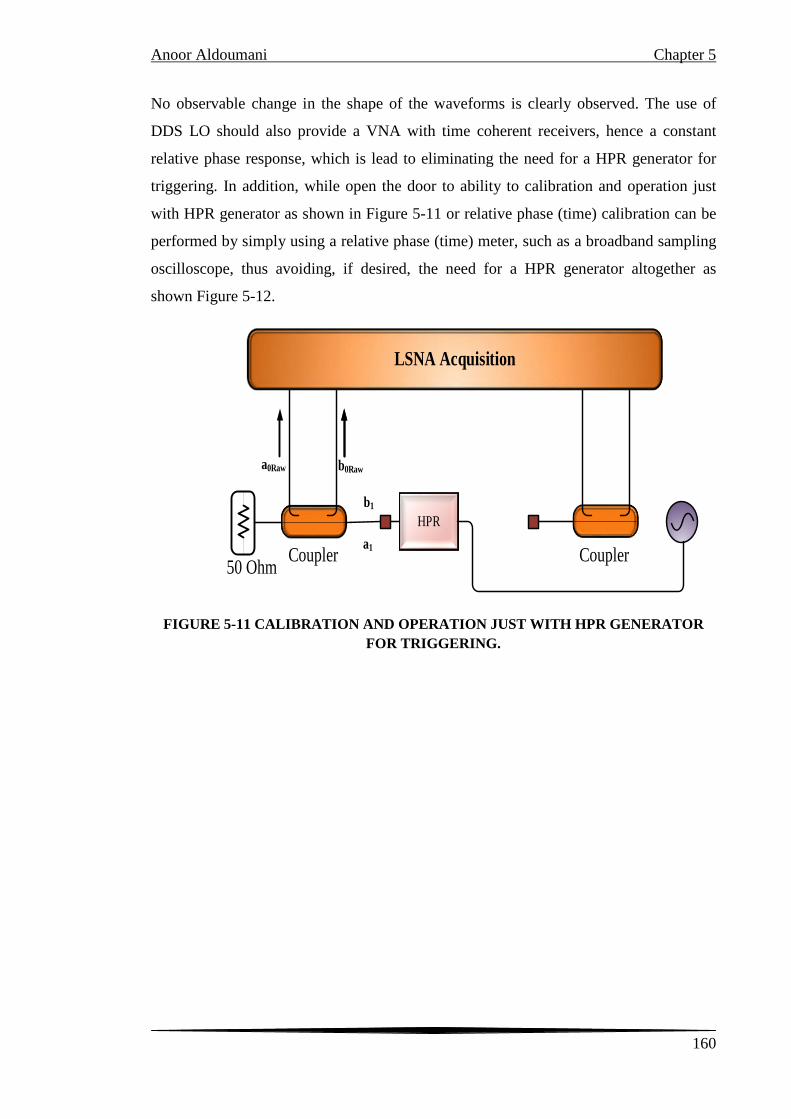
Anoor Aldoumani Chapter 5
160
No observable change in the shape of the waveforms is clearly observed. The use of
DDS LO should also provide a VNA with time coherent receivers, hence a constant
relative phase response, which is lead to eliminating the need for a HPR generator for
triggering. In addition, while open the door to ability to calibration and operation just
with HPR generator as shown in Figure 5-11 or relative phase (time) calibration can be
performed by simply using a relative phase (time) meter, such as a broadband sampling
oscilloscope, thus avoiding, if desired, the need for a HPR generator altogether as
shown Figure 5-12.
LSNA Acquisition
a0Raw b0Raw
Coupler Coupler
HPRa1
b1
50 Ohm
FIGURE 5-11 CALIBRATION AND OPERATION JUST WITH HPR GENERATOR FOR TRIGGERING.

Anoor Aldoumani Chapter 5
161
LSNA Acquisition
a0Raw b0Raw
Coupler Couplera1
b1
10MHz
4-Channel Microwave Sampler
RCVR RCVR RCVRRCVR
SamplerHead
Trigger
f0-nf0f0
FIGURE 5-12 CALIBRATION AND OPERATION WITH PHASE METER.
5.5.1.2 RECEIVER
Consider now a VNA based LSNA system using the Rohde and Schwarz ZVA-67, in
this case the phase of the LO while not known, when sweeping the frequency, should no
longer vary and be repeatable between measurements. This should happen since the
ZVA-67 integrates multiple internal DDS signal sources, for both the local oscillator
and the device excitation as result all the internal sources should be time coherence,
hence also any IF down converted signal.
In this case the VNA (ZVA-67) should has ability to following a relative phase
calibration therefore, the VNA (ZVA-67) will able to do directly measure the Fourier
coefficients 𝑛(𝜔)and 𝐵𝑛(𝜔)with respect to a common time trigger as well as ability to
do accurately measure 𝐴𝑛(𝑡) and 𝐵𝑛(𝑡)without the requirement of attaching a HPR
generator to an additional receiver. this advantage give an ability to correct the phase
during measurement by two ways, the first method by using HPR generator or relative
phase meter a broadband sampling oscilloscope. This stage consist of practical
investigating for the possibility of utilized the “time coherence” of the ZVA in mode of
the measurement operation.

Anoor Aldoumani Chapter 5
162
LO
R&S ZVA 67GHz
b‘0a‘0
S2a0 b0
f0
f0±ψψ ψ
FIGURE 5-13 ZVA LO SOURCES UTILIZE DIGITAL SYNTHESISERS.
The next investigation involves testing the time coherence of the receivers in the VNA
(ZVA-67). These involve measuring the phase jitter which is observed over time. It can
be described as a variation in phase with time for 𝑎1,𝑅𝐴𝑊(𝜔) and 𝑏1,𝑅𝐴𝑊(𝜔) as a
function of frequency. Figure 5-13 shows the hardware configuration of ZVA, the
ZVA67 was configured to perform swept frequency measurements on a 1 GHz grid
from 1 GHz to 50 GHz. A subroutine was written to collect a dataset sequence; the raw
ZVA data from port 1, the measured frequency response 𝑎1,𝑅𝐴𝑊(𝜔) and 𝑏1,𝑅𝐴𝑊(𝜔), for
each one minute interval during the first hour followed by 30 minutes intervals for the
next 24 hrs.

Anoor Aldoumani Chapter 5
163
FIGURE 5-14 14MEASURED PHASE JITTER OBSERVED OVER A 24 HR PERIOD FOR 𝒃𝒓𝒂𝒘~ AS FUNCTION OF FREQUENCY.
FIGURE 5-15 MEASURED PHASE JITTER OBSERVED OVER A 24 HR PERIOD FOR 𝒂𝒓𝒂𝒘~ AS FUNCTION OF FREQUENCY.
The Figure 5-14 and Figure 5-15 show (𝑏0𝑅𝑎𝑤 and 𝑎0𝑅𝑎𝑤 ) which is obtained as results
for measuring relative phase for 24 hours. The plots show the relative phase variation
over this period as a dot for each frequency at each sample time, these dots then show
the total variation for each frequency over this time. It is seen that while the measured
phase of each signal is not constant and varies randomly, the two receivers are tracking
each other. This indicates that the source of the variation is not in the receivers but the
source (LO), which is common to both receivers. This means for each frequency the
phase of the LO changes by a constant amount, and so can be calibrated out. As
conclusion: the measured relative phase is not randomized anymore, this means for each
sweeping of frequency to change the phase for LO by an known amount. Since these
travelling wave signals have common internal excitation and LO sources.

Anoor Aldoumani Chapter 5
164
Of critical interest is the variation in the measured relative phase response Δ𝜙 over time
of the multiple sources, Δ𝜙 consist of (Δ𝑡𝑃 ) due to the variation in source and
(Δ𝑡𝐿𝑂)due to variation in local oscillator, time, normalized to first measurement dataset.
The measured dataset at the 𝑖th time interval is thus given by;
𝒂𝟏,𝑹𝑨𝑾𝒊 (𝝎) = 𝒂𝟏,𝑹𝑨𝑾
𝟎 (𝝎)𝒆𝒋𝚫𝝓 = 𝒂𝟏,𝑹𝑨𝑾𝟎 (𝝎)𝒆𝒋𝝎(𝚫𝒕𝑷+𝚫𝒕𝑳𝑶) EQUATION 5-1
𝒃𝟏,𝑹𝑨𝑾𝒊 (𝝎) = 𝒃𝟏,𝑹𝑨𝑾
𝟎 (𝝎)𝒆𝒋𝚫𝝓 = 𝒃𝟏,𝑹𝑨𝑾𝟎 (𝝎)𝒆𝒋𝝎(𝚫𝒕𝑷+𝚫𝒕𝑳𝑶) EQUATION 5-2
Figure 5-16and Figure 5-17 shown the normalization 𝑎0𝑅𝑎𝑤 and 𝑏0𝑅𝑎𝑤 normalized to
first measurement in dataset, which is obtained during 24 hours to fundamental
frequency as function for frequency. These figures shown there is a considerable scatter
observed for 𝑎0𝑅𝑎𝑤 and 𝑏0𝑅𝑎𝑤 and difference in relative phase between fundamental
and each harmonics. However, ratio measurement found the phase drift 0.01 deg and
maximum phase uncertainty +/-0.16 deg.
FIGURE 5-16 MEASURED PHASE JITTER OBSERVED OVER A 24 HR PERIOD FOR RAW 𝒂𝟎, AS A FUNCTION OF FREQUENCY. AVERAGE VALUES IS ALSO
IDENTIFIED WITH DOT.

Anoor Aldoumani Chapter 5
165
FIGURE 5-17 MEASURED PHASE JITTER OBSERVED OVER A 24HR PERIOD FOR RAW 𝒃𝟎, AS A FUNCTION OF FREQUENCY. AVERAGE VALUES IS ALSO
IDENTIFIED WITH DOT.
From Figure 5-16 and Figure 5-17 can observe the 𝑎0𝑅𝑎𝑤 and 𝑏0𝑅𝑎𝑤 have same (same
scatter is just because coherence a common LO which is lead to the pattern of LO and
source phase ) distribution scattering as function for frequency during period 24 hours
this due to DDS technology used in sources and receivers of ZVA-67 as shown in
equation 5-3 and 5-4.
𝒂𝟎′𝒊 = 𝒂𝟎𝒆𝒋𝝎∆𝒇(𝒕−(𝝉𝒔−𝝉𝑳𝑶)) EQUATION 5-3
𝒃𝟎′𝒊 = 𝒃𝟎𝒆𝒋𝝎∆𝒇(𝒕−(𝝉𝒔−𝝉𝑳𝑶)) EQUATION 5-4
For that the scatter should not be observed in the ratio 𝑏1,𝑅𝐴𝑊𝑖 (𝜔)
𝑎1,𝑅𝐴𝑊𝑖 (𝜔)
𝑆11𝑅𝑎𝑤as shown in
Figure 5-18, this due to these travelling wave signals have common LO sources and
internal excitation as mentioned before.

Anoor Aldoumani Chapter 5
166
FIGURE 5-18 MEASURED PHASE JITTER OBSERVED OVER A 24HR PERIOD FOR RAW S11, AS A FUNCTION OF FREQUENCY. AVERAGE VALUES IS ALSO
IDENTIFIED WITH DOT.
By observing the time jitter as function of frequency for over a 24 hours period for
𝑏1,𝑅𝐴𝑊` (𝜔) and 𝑎1,𝑅𝐴𝑊
` (ω) they are identical, this is shown in Figures 5-19 and 5-20.
This verifies the results shown by the previous measurements in Figures 5-14 and 5-15,
that the apparent increase of this relative phase scatters with frequency is consistent
with the source being related to frequency independent timing jitter. This effect has now
been shown in both the time in Figures 5-19 and 5-20, in the DDS internal signal
generators; the LO signal generator and/or phase jitter 𝜔𝑡𝐿𝑂 , port signal generator,
phase jitter 𝜔∆𝑡𝐿𝑂. By focusing across frequency see that thus phase drift is simply an
associated to as common time jitter for all frequencies.

Anoor Aldoumani Chapter 5
167
FIGURE 5-19 MEASURED TIME JITTER OBSERVED OVER A 24HR PERIOD FOR 𝒂𝟎,𝑹𝑨𝑾
~ (𝝎) (Ω) AS A FUNCTION OF FREQUENCY.
FIGURE 5-20 MEASURED TIME JITTER OBSERVED OVER A 24HR PERIOD FOR 𝒃𝟎,𝑹𝑨𝑾
~ (𝝎)AS A FUNCTION OF FREQUENCY.
In any case, A closer inspection for result obtained from measured the time jitter for
𝑎0𝑅𝑎𝑤 and 𝑏0𝑅𝑎𝑤 that not all this time jitter, +/- 1.6 spec, is random and that a major
component is in reality a time drift term that is identical (coherent) across the measured
50 GHz bandwidth, as clearly shown in Figure 5-21 A and 24 hours as shown in
Figure 5-21B for 𝑎0𝑅𝑎𝑤 as a function of observation time at selected frequencies as well
as Figure 5-22 A and Figure 5-22 B obtained as result for measured time jitter observed
over for 1 hour and 24 hours for 𝑏0𝑅𝑎𝑤 as a function of observation time at selected
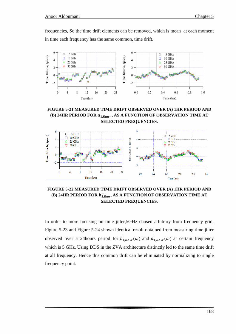
Anoor Aldoumani Chapter 5
168
frequencies, So the time drift elements can be removed, which is mean at each moment
in time each frequency has the same common, time drift.
FIGURE 5-21 MEASURED TIME DRIFT OBSERVED OVER (A) 1HR PERIOD AND (B) 24HR PERIOD FOR 𝒂𝟏,𝑹𝒂𝒘
~ , , AS A FUNCTION OF OBSERVATION TIME AT SELECTED FREQUENCIES.
FIGURE 5-22 MEASURED TIME DRIFT OBSERVED OVER (A) 1HR PERIOD AND (B) 24HR PERIOD FOR 𝒃𝟏,𝑹𝒂𝒘
~ , AS A FUNCTION OF OBSERVATION TIME AT SELECTED FREQUENCIES.
In order to more focusing on time jitter,5GHz chosen arbitrary from frequency grid,
Figure 5-23 and Figure 5-24 shown identical result obtained from measuring time jitter
observed over a 24hours period for 𝑏1,𝑅𝐴𝑊` (𝜔) and 𝑎1,𝑅𝐴𝑊
` (𝜔) at certain frequency
which is 5 GHz. Using DDS in the ZVA architecture distinctly led to the same time drift
at all frequency. Hence this common drift can be eliminated by normalizing to single
frequency point.

Anoor Aldoumani Chapter 5
169
FIGURE 5-23 MEASURED TIME JITTER OBSERVED OVER A 24HR PERIOD FOR 𝒂𝟏,𝑹𝒂𝒘
~ AT A 5 GHZ.
FIGURE 5-24 MEASURED TIME JITTER OBSERVED OVER A 24HR PERIOD FOR 𝒃𝟏,𝑹𝒂𝒘
~ AT A 5 GHZ.
Critically, can understand from above the process of determine time varying signals
𝑎𝑛(𝑡) & 𝑏𝑛(𝑡) which is obtained from compute the measured Fourier coefficients
𝑎𝑛~(𝑤) and 𝑏𝑛~(𝑤) will not effect by the coherent time drift or could say the coherent
time drift has no influence on the determined time varying signals 𝑎𝑛(𝑡)& 𝑏𝑛(𝑡)this

Anoor Aldoumani Chapter 5
170
happen when time aligning the individually computed spectral components since it is
common for all.
As shown in Figure 5-25 the ZVA-67 has residual measured LO time (phase) jitter after
disarmament of the coherent drift component is observed to be below +/- 0.3 psec. The
above investigations prove that the ZVA-67 is a “time coherent” system, which, after
relative phase (time) calibration should be able to perform accurate measurement of
time varying signals 𝑎𝑛(𝑡) & 𝑏𝑛(𝑡) without requiring a HPR generator connected to an
occupying an additional channel.
FIGURE 5-25 MEASURED RESIDUAL TIME JITTER OBSERVED OVER A 24HR PERIOD FOR 𝒂𝟏,𝑹𝒂𝒘
~ , AS A FUNCTION OF FREQUENCY AFTER REMOVAL OF THE COHERENT DRIFT COMPONENT (DETERMINED IN THIS CASE AT 5 GHZ).
AN IDENTICAL RESULT IS ACHIEVED FOR 𝒃𝟏,𝑹𝒂𝒘~ .

Anoor Aldoumani Chapter 5
171
5.5.1.4 PHASE CALIBRATION
The ZVA-67 is a “time coherent” system able to perform accurate measurement of time
varying signals 𝑎𝑛(𝑡) & 𝑏𝑛(𝑡)with or without requiring a HPR generator .This led to
ability correct the phase by traditional method (using HPR generator) or without by
using phase meter determine the phase of 𝑎𝑛(𝑡) & 𝑏𝑛(𝑡)as shown in Figure 5-26 and
Figure 5-27.
LSNA Acquisition
a0Raw b0Raw
Coupler Couplera1
b1
10MHz
4-Channel Microwave Sampler
RCVR RCVR RCVRRCVR
SamplerHead
Trigger
f0-nf0f0
FIGURE 5-26 GENERIC LSNA CONFIGURATION FOR ZVA RELATIVE PHASE CALIBRATION.

Anoor Aldoumani Chapter 5
172
R&S ZVA- 67GHz
Trigger “Time” Meter
bTM
f0
LO
b´0a´0
a0 b0
nf0
a1
b1
DSA8200 Digital Sampling Oscilloscope
S1
S4
FIGURE 5-27 HARDWARE CONFIGURATION FOR ZVA RELATIVE PHASE CALIBRATION.
4.5.2 CALIBRATION
No measurement system is perfect, therefore the LSNA performs un-calibrated or ‘raw’
measurements by other words the LSNA measurements contain errors resulting from
systematic, random and drift components as mentioned in pervious chapter, therefore
full calibration is necessary to minimized systematic errors [1-4].
This section deal with full calibration for NVNA (ZVA-67GHz) after approved ZVA-67
phase coherent, calibration is technical process used to characterizing the measurement
system so that systematic errors can be minimized from the measurement result and
transfer the reference planes for measurement system from ports reference planes to
desired DUT reference planes by calculate the 8 coefficients of the error model defined
in frequency domain [6-8, 13-16].
Before proceeding with the calibration aspects, it is valuable to consider the equipment
schematic of a NVNA's this is due to the fact that there are three types of (LSNA)
systems and ZVA 67-GHz considered is Mixer-based vector (NVNAs). The outline of
the calibration measurement consists of three stages which should be performed for
every single measured frequency:-

Anoor Aldoumani Chapter 5
173
1. Relative calibration(Small Signal calibration),
2. Phase calibration,
3. Power calibration.
The Figure 5-28 shown three stages of full calibration for NVNA.
FIGURE 5-28 STEPS NECESSARY FOR CALIBRATION NVNA.
For a two-port device measurements this operation is achieved via the following
mathematical transformation;
⎣⎢⎢⎢⎡𝒂𝟏,𝑪𝑶𝑹(𝝎)𝒃𝟏,𝑪𝑶𝑹(𝝎)𝒂𝟐,𝑪𝑶𝑹(𝝎)𝒃𝟐,𝑪𝑶𝑹(𝝎)⎦
⎥⎥⎥⎤
= 𝒌(𝝎)[𝒆(𝝎)]
⎣⎢⎢⎢⎡𝒂𝟏,𝑹𝑨𝑾(𝝎)𝒃𝟏,𝑹𝑨𝑾(𝝎)𝒂𝟐,𝑹𝑨𝑾(𝝎)𝒃𝟐,𝑹𝑨𝑾(𝝎)⎦
⎥⎥⎥⎤ EQUATION 5-5
Where
[𝒆(𝝎)] =
𝟏 𝒆𝟏𝟐(𝝎) 𝟎 𝟎𝒆𝟐𝟏(𝝎) 𝒆𝟐𝟐(𝝎) 𝟎 𝟎𝟎 𝟎 𝒆𝟑𝟑(𝝎) 𝒆𝟑𝟒(𝝎)𝟎 𝟎 𝒆𝟒𝟑(𝝎) 𝒆𝟒𝟒(𝝎)
EQUATION 5-6
The error model [𝑒⟨𝑤⟩] generated by calibration process, is used to describes the raw
data and reference plane data.

Anoor Aldoumani Chapter 5
174
The linear calibration (small signal calibration or relative calibration) in reality is
exactly the same as for a VNA calibration and is performed by using a classical VNA
calibration on a selected frequency grid, the calibration procedures executed for instance
be obtained by a Short-Open-Load-Thru (SOLT), Thru-Reflect-Load (TRL), Load-
Reflect-Match (LRM), or other calibration standards. The relative calibration provides
the following individual error coefficient values: for port 1 𝑒00 , 𝑒11 and 𝑒10𝑒01 and for
port 2 𝑒22 , 𝑒33 and 𝑒32𝑒23 , the other products: 𝑒10𝑒32 and 𝑒01𝑒23 obtained from
connected Thru standard between port 1 and port 2. The error matrix [𝑒(𝜔)] represents
all error terms obtained during small signal calibration, should be mentioned S-
parameters are a ratio measure [13-20].
At the end of this stage the relative calibration ended, the ZVA-67 GHz can be used as a
normal VNA to measure S-parameter for DUT but S-parameter do not have ability to
characterize nonlinear system, therefore the determination of the additional vector error
term 𝑘(𝜔) is considered necessary step for LSNA calibration and operation. This
usually includes a two-step process where the magnitude and relative period of 𝑘(𝜔)
are determined independent [13-20].
The aim from power calibration is to determine the magnitude of 𝑘(𝑤) which is mean
absolute power. During this stage a power meter is connected to the reference port
directly, in this case it is connected to port 1 in order to enable the power meter from
reading the absolute value of flowing power into the DUT which, in this case, is the
magnitude of | 𝑎1,𝐶𝑂𝑅 (𝜔)| . It is equal 𝑡𝑜 |𝑎 𝑃𝑜𝑤𝑒𝑟 (𝜔)| the magnitude of |𝑘(𝜔)| is
computed as follows;
|𝒌(𝝎)| = |𝒂𝑷𝒐𝒘𝒆𝒓(𝝎)|
𝒆𝟐𝟏(𝝎)𝒂𝟏,𝑹𝑨𝑾(𝝎)+𝒆𝟐𝟐(𝝎)𝒃𝟏,𝑹𝑨𝑾(𝝎) EQUATION 5-7
It is worth to mention, if a CW frequency stimulus signal is applied and can be stepped-
thru the calibrated frequency grid [13-20].
The final step was determines the relative phase which is achieved by connecting a HPR
generator a known harmonically rich stimulus, in this case port 1. Calibration NVNA

Anoor Aldoumani Chapter 5
175
can only be achieved if the HPR generator is able to generate a stimulus that has
frequency components covering the desired frequency grid. As the requirement for a
triggering HPR generator standard during the measurement step has been removed, its
complete elimination from the phase calibration step would further simplify the system
architecture.
Consider instead an alternative approach to relative phase calibration: To determine the
relative phase, a phase meter is connected to the reference port which is in this case port
1. In this demonstration, a Tektronix DSA 8200 sampling scope with high frequency
(67GHz) sampling head is used as the relative phase meter. To ensure a common time
reference for the relative phase measurements, the Tektronix sampling scope is
triggered using one of the spare internal ZVA-67 DDS signal sources, as shown in
Figure 5-29, which in this case is set to an appropriate reference frequency of 1 GHz.
R&S ZVA- 67GHz
Trigger “Time” Meter
bTM
f0
LO
b´0a´0
a0 b0
nf0
a1
b1
DSA8200 Digital Sampling Oscilloscope
S1
S4
FIGURE 5-29 HARDWARE CONFIGURATION FOR ZVA RELATIVE PHASE CALIBRATION USING A PHASE METER.
A stepped frequency CW stimulus signal is then applied to the reference port (Perform a
sequence of simultaneous ZVA-67 and scope measurements 𝑓𝑜 ,2𝑓𝑜 ,3𝑓𝑜 ... 𝑛𝑓𝑜 ), and
since the angle ∠𝑎1,𝐶𝑂𝑅(𝜔) is now directly measured, it is equal to ∠𝑎𝑃ℎ𝑎𝑠𝑒(𝜔) (the
phase component of the Fourier transformed sampling scope measured waveform), the
relative phase ∠𝑘(𝜔) is computed as follows;

Anoor Aldoumani Chapter 5
176
∠𝒌(𝝎) = ∠𝒂𝑷𝒉𝒂𝒔𝒆(𝝎)− ∠𝒆𝟐𝟏(𝝎)𝒂𝟏,𝑹𝑨𝑾(𝝎) + 𝒆𝟐𝟐(𝝎)𝒃𝟏,𝑹𝑨𝑾(𝝎) EQUATION 5-8
In this case, a simple, easily generated, single frequency signal of appropriate power
level is all that is required for phase calibration.
Using the internal ZVA-67 sources ensures that LSNA operation can be achieved over
its full bandwidth of 67GHz. At this point, the ZVA-67 LSNA system is fully calibrated
and ready to perform coherent measurements of time varying signals 𝐴𝑛(𝑡) and 𝐵𝑛(𝑡) at
all four ports. This is now possible as the fourth port is no longer required as a
reference receiver to measure the HPR.
The LSNA system is now fully calibrated, at the verification can be performed by
comparing the ZVA-67 and scope to measure a waveform at the reference port, which
in this case port1. Both instruments should have same result as shown in Figure 5-30.
FIGURE 5-30 SYNTHESIZED POWER AMPLIFIER TYPE TIME VARYING SIGNAL AT 1 GHZ.
Typical results achieved are shown in Figure 5-30, both ZVA -67 and scope measure
the same waveform.

Anoor Aldoumani Chapter 5
177
4.5.3 CALIBRATION VALIDATION
This section is to verify the functionality of the calibrated ZVA-67 based on LSNA
system. To achieve this measurement were performed using the experimental setup
shown in Figure 5-31.
LO
nf0
R&S ZVA 67GHz
f0
a1
b1
b´0a´0
Trigger
“Time” Meter
bTM
S2
S1
a0 b0mf0
S4
DSA8200 Digital Sampling Oscilloscope
FIGURE 5-31 EXPERIMENTAL SETUP USED FOR ZVA WAVEFORM MEASUREMENT VERIFICATION.
Figure 5-31 shown two of the ZVA’s internal DDS sources set to different frequencies,
power levels and phases, are combined in order to synthesize complex time varying
signals at one of the calibrated port (in this case port 1). Both the ZVA-67 and the
Tektronix sampling scope measure these signals simultaneously.
Figure 5-32 shown waveform measured by using Scope and ZVA-67 before phase
correction and Figure 5-33 shown waveform measured by Scope and ZVA-67 after
phase correction by phase meter. In this case the internal source for ZVA-67 S1 set in
this case to 1 GHz and S2 to 2 GHz and Scope trigger S4 to 1GHz (fundamental
frequency).

Anoor Aldoumani Chapter 5
178
FIGURE 5-32 RF WAVEFORM MEASURED BY ZVA AND SCOPE BEFORE CORRECT THE PHASE BY PHASE METER. (AT 1GHZ AND 2GHZ)
FIGURE 5-33 RF WAVEFORM MEASURED BY ZVA AND SCOPE AFTER CORRECT THE PHASE BY PHASE METER. (AT 1 GHZ AND 2GHZ)
Figure 5-34 shown and their example for waveform measured by using Scope and
ZVA-67 before phase correction and Figure 5-35 shown waveform measured by Scope
and ZVA-67 after phase correction by phase meter.
In this case the internal source for ZVA-67 S1 set in this case to 1 GHz and S2 to 3 GHz
and scope trigger S4 at 1GHz (fundamental frequency).

Anoor Aldoumani Chapter 5
179
FIGURE 5-34 RF WAVEFORM MEASURED BY ZVA AND SCOPE UNCORRECTED THE PHASE BY PHASE METER.(AT 1 GHZ AND 3 GHZ)
FIGURE 5-35 RF WAVEFORM MEASURED BY ZVA AND SCOPE AFTER CORRECTED THE PHASE BY PHASE METER.(AT 1 GHZ AND 3 GHZ)
Figure 5-36 shown another example for waveform measured by using Scope and ZVA-
67 before phase correction and Figure 5-37 shown waveform measured by Scope and
ZVA-67 after phase correction by phase meter. In this case the internal source for ZVA-
67 S1 set in this case to 1 GHz and S2 to 4 GHz and Scope trigger by S4 at 1GHz
(fundamental frequency).

Anoor Aldoumani Chapter 5
180
FIGURE 5-36 RF WAVEFORM MEASURED BY ZVA AND SCOPE BEFORE UNCORRECTED THE PHASE BY PHASE METER.(AT 1 GHZ AND 4 GHZ)
FIGURE 5-37 RF WAVEFORM MEASURED BY ZVA AND SCOPE BEFORE CORRECTED THE PHASE BY PHASE METER. (AT 1 GHZ AND 4 GHZ).
The Figure 5-38 shown other example for waveform measured by using Scope and
ZVA-67 before phase correction and Figure 5-39 shown waveform measured by Scope
and ZVA-67 after phase correction by phase meter, which is match the result in both
system. It is useful to mention the internal source for ZVA-67 S1 set in this case to 2
GHz and S2 to 5 GHz and trigger the Scope by S4 at 1GHz (frequency).

Anoor Aldoumani Chapter 5
181
FIGURE 5-38 RF WAVEFORM MEASURED BY ZVA AND SCOPE BEFORE UNCORRECTED THE PHASE BY PHASE METER. (AT 2GHZ AND 5 GHZ)
FIGURE 5-39 RF WAVEFORM MEASURED BY ZVA AND SCOPE AFTER CORRECTED THE PHASE BY PHASE METER. (AT 2GHZ AND 5 GHZ)
More tests lead to typical results achieved are shown in Figure 5-40,
Figure 5-41,Figure 5-42 and, indicating that the displayed ZVA DDS
waveforms𝐴1,𝐶𝑂𝑅𝑅(𝑡), computed from vector error correct measurements performed in
the frequency domain, 1,𝐶𝑂𝑅(𝜔) and 𝐵2,𝐶𝑂𝑅(𝜔) , are identical to those measured
directly in the time domain with the Tektronix Sampling Scope 𝐴𝑠𝑐𝑜𝑝𝑒(𝑡). The results

Anoor Aldoumani Chapter 5
182
confirm that the calibrated ZVA LSNA system is fully functional and can perform
waveform measurements over its full bandwidth. The relative phase uncertainly
observed in these measurements is again consistent with the previously observed value
of +/- 0.3 psec.
FIGURE 5-40 SYNTHESIZED POWER AMPLIFIER TYPE TIME VARYING SIGNAL CONTAINING FREQUENCY COMPONENTS AT 10 (FUNDAMENTAL
FREQUENCY) GHZ AND 20,30 AND 40 GHZ HARMONICS.

Anoor Aldoumani Chapter 5
183
FIGURE 5-41 SYNTHESIZED POWER AMPLIFIER TYPE TIME VARYING SIGNAL CONTAINING FREQUENCY COMPONENTS AT 20 GHZ AND 40 GHZ.
FIGURE 5-42 SYNTHESIZED MIXER TYPE SIGNALS CONTAINING FREQUENCY COMPONENTS AT DIFFERENT FREQUENCIES.

Anoor Aldoumani Chapter 5
184
FIGURE 5-43 SYNTHESIZED MIXER TYPE SIGNALS CONTAINING FREQUENCY COMPONENTS AT DIFFERENT FREQUENCIES.
Calibration is done using internal sources and a phase meter. No phase standard
required, no bandwidth limitations and no frequency restrictions. VNA systems with
digital sources, both RF stimulus and LO, can after calibration provide for RF I-V
waveform measurements.

Anoor Aldoumani Chapter 5
185
4.6 SUMMARY
A new approach for operating and calibrating emerging VNA systems use in LSNA
measurement systems has been developed, implemented and verified. A key feature of
this approach is that both the operation and calibration of the VNA based LSNA system
is achieved without the requirement of a harmonic phase reference HPR generator.
The implementation exploits the fact that emerging VNA architectures, e.g. the Rohde
and Schwarz ZVA-67 incorporate internal signal and local oscillator (LO) sources based
on Direct Digital Synthesis. The use of such DDS components provides a VNA
receiver that is both repeatable and coherent in terms of relative phase over its full
frequency bandwidth, in this case to within +/- 0.3 psec. DDS based sources remove the
need for a phase reference during measurement, frees up one of the sources allowing 1-
in-3 out operation with no additional sources. Also opens potential for full 4 port
measurements with time domain information. No phase drift between drive signal and
load-pull signals means convergence is faster, and makes very high frequency load-pull
possible. Can also revisit past known impedance states (could be very useful for
production testing) The calibration approach developed uses a relative phase (time) meter, i.e. a sampling
oscilloscope to perform the relative phase (time) calibration. Since calibration in this
case is carried out using the VNA internal sources and a broadband sampling scope,
there are reduced restrictions on the frequency grid and bandwidth. Importantly, as no
dedicated channel is required for triggering during waveform measurements, all four
VNA ports are available for DUT characterization, eliminating the need for
multiplexing measurement signals, and allowing a simple and rapid measurement
approach.

Anoor Aldoumani Chapter 5
186
4.7 REFERENCE
1- Tasker, P.J., Practical waveform engineering. Microwave Magazine,
IEEE, 2009. 10(7): p. 65-76.
2- Golio, M. and J. Golio, RF and Microwave Circuits, Measurements,
and Modeling. 2007: Taylor & Francis.
3- Pailloncy, G., et al., Large-Signal Network Analysis Including the
Baseband. Microwave Magazine, IEEE, 2011. 12(2): p. 77-86.
4- Benedikt, J., et al., High-power time-domain measurement system
with active harmonic load-pull for high-efficiency base-station
amplifier design. Microwave Theory and Techniques, IEEE
Transactions on, 2000. 48(12): p. 2617-2624.
5- Blockley, P., D. Gunyan, and J.B. Scott. Mixer-based, vector-
corrected, vector signal/network analyzer offering 300kHz-20GHz
bandwidth and traceable phase response. in Microwave Symposium
Digest, 2005 IEEE MTT-S International. 2005.
6- Verspecht, J., Large-signal network analysis. Microwave Magazine,
IEEE, 2005. 6(4): p. 82-92.
7- Rohde & Schwarz USA, I., R&S ® ZVA Vector Network Analyzer
High performance up to 110GHz with up to four test ports.
8- Broeck, T.V.d. and J. Verspecht. Calibrated vectorial nonlinear-
network analyzers. in Microwave Symposium Digest, 1994., IEEE
MTT-S International. 1994.
9- Williams, D., P. Hale, and K.A. Remley, The Sampling Oscilloscope
as a Microwave Instrument. Microwave Magazine, IEEE, 2007. 8(4):
p. 59-68.
10- NI. Understanding Direct Digital Synthesis (DDS). [cited 2015 Oct
10, 2015]; Available from: www.ni.com.
11- Agilent, Agilent U9391C/F/G Comb Generators.

Anoor Aldoumani Chapter 5
187
12- Systems, S.R. Direct Digital Synthesis Application Note #5. Available
from: www.thinkSRS.com.
13- Roblin, P., Nonlinear RF Circuits and Nonlinear Vector Network
Analyzers: Interactive Measurement and Design Techniques. 2011:
Cambridge University Press.
14- Van Moer, W. and Y. Rolain. An improved broadband conversion
scheme for the large signal network analyzer. in Microwave
Symposium Digest, 2005 IEEE MTT-S International. 2005.
15- Van Moer, W. and L. Gomme, NVNA versus LSNA: enemies or
friends? Microwave Magazine, IEEE, 2010. 11(1): p. 97-103.
16- Verspecht, J., Calibration of a Measurement System for High
Frequency Nonlinear Devices. 1995, Vrije Universiteit Brussel.
17- Jarndal, A. and G. Kompa, Large-Signal Model for AlGaN/GaN
HEMTs Accurately Predicts Trapping- and Self-Heating-Induced
Dispersion and Intermodulation Distortion. Electron Devices, IEEE
Transactions on, 2007. 54(11): p. 2830-2836.
18- Agilent, High Power Amplifier Measurements Using Agilent’s
Nonlinear Vector Network Analyzer Application Note 1408-19. 2010.
19- Scott, J.B., P.S. Blockley, and A.E. Parker. A new instrument
architecture for millimetre-wave time-domain signal analysis. in
ARFTG Conference Digest Spring, 2004. 63rd. 2004.
20- Verspecht, J., F. Verbeyst, and M. Vanden Bossche. Network
Analysis Beyond S-parameters: Characterizing and Modeling
Component Behaviour under Modulated Large-Signal Operating
Conditions. in ARFTG Conference Digest-Fall, 56th. 2000.
End Chapter

Anoor Aldoumani Chapter 6
188
6 CHAPTER 6
CONCLUSIONS AND FUTURE WORK
The objective of this research was to improve the calibration and functionality of
waveform measurement systems. The focus of this research has been split into two main
sections:-
1) Enhancement vector calibration of any VNA measurement system to increase the S-
parameter calibrated accuracy, especially at the edge of the Smith Chart and 2)
operation and calibration of VNA based on large signal network analyzer systems
without using phase reference. This thesis discussed the development of error models
for measurement system, calibration algorithms, calibration kits, architecture of
nonlinear measurement systems, and calibration of each type of non-linear measurement
system.
The common focus in both of these areas has been utilising the RF IV waveform
measurement system reading to increase the accuracy of error terms which in turn
increased the accuracy of the measurement system and calibration and operation VNA
base on LSNA without required to phase standard to obtain system not suffering from
bandwidth limitations and frequency restrictions with high accuracy.
5.1 CONCLUSIONS
Two main concepts are investigated in this thesis. The first concept emerged in Chapter
2 with a literature review for a theoretical analysis of S-parameter starting by error
model for 1 Port networks, 2 Ports networks, calibration algorithm for SLOT and TRL,
calibration tools kits and small overview about uncertainty in small signal calibration.

Anoor Aldoumani Chapter 6
189
Chapter 3 introduce the new approach to improving vector measurement accuracy
developed in this work, especially near the edge of the Smith Chart, very important in
load-pull measurement systems. Improved measurement accuracy after vector
calibration, is achieved by exploiting the load-pull capability during calibration to
minimise the impact of measurement errors on the raw calibration standards data before
it is utilised in the traditionally implemented LRL/TRL calibration algorithm. This new
approach eliminates the need to utilise complex optimisation algorithms post
calibration. The proposed method has been tested and applied to actual measurement
data, as well as in investigating the relationship between reflection coefficient and
quality of raw data obtained during calibration using a load pull system.
The second part of this thesis addresses augmentations about wave meter and it’s aimed
to more develop in the non-linear measurement efficiency of the large signal network
analyzer systems, which lead to the development of its applicability for use in helping
design RFPA. Chapter 4 extended the review and insight about existing large signal
network analyser measurement systems and briefly discussed the architecture and
advantages and disadvantages of each type. A new approach to calibration is
introduction in Chapter 5. The present LSNA measurement systems provide
measurement capabilities to perform full error correction in frequency domain and
present the result in voltage and current waveform in time domain measurements using
a harmonic phase reference generator which limits bandwidth and frequency restrictions
during measurement. Therefore a new approach is presented in Chapter 5 that allows a
Vector Network Analyzer to be operated as a Large Signal Network Analyzer without
the need for a harmonic phase reference generator. This mode of operation exploits the
architecture of the Rohde and Schwarz ZVA-67, which incorporates internal signal and
local oscillator sources based on direct digital synthesis. This unique capability leads to
a Vector Network Analyzer based Large Signal Network Analyzer configuration that
incorporates time coherent sources and receivers. This feature combined with a
modified calibration procedure, allows the instrument, to provide error corrected RF
current and voltage waveform measurements, requiring only internal signal sources and
an external phase meter. This approach simplifies the Large Signal Network Analyzer
architecture and removes the complexities and bandwidth limitations introduced when
employing a harmonic phase reference generator. Further development of the LSNA
was achieved to improve the measurement system, particularly this technical make all

Anoor Aldoumani Chapter 6
190
four VNA ports are available for DUT characterization, eliminating the need for
multiplexing measurement signals, and allowing a simple and rapid measurement
approach. This method can provide a full calibration for N ports VNAs and be used in
LSNA allowing capable systems to provide mixer and antenna measurements.
5.2 FUTURE WORK
The main development of the measurement throughout this work has certainly been
achieved with respect to improving the vector measurement accuracy and the
functionality of large signal network analyzer-systems. However, there is still a lot that
can be done to support previous efforts as well as the developments contained in this
thesis. The LSNA has been developed to the stage where architecture has been
implemented to measure waveform without using a harmonic phase reference standard
for continuous signals and modulation signals. A drawback of this approach is that
coherent phase will be lost after harmonic 15 due to a +/- 1.6 time jitter of the
oscilloscope used to collect the phase of the calibration wave signal. This problem can
be overcome the problem by using new technique for phase alignment and real time
oscilloscope.
Accurate predictions of the vector measurement, especially near the edge of the Smith
Chart, of load-pull measurement systems, have been shown to improved when using the
load-pull capability during calibration to minimise the impact of measurement errors on
the raw data of the calibration standards before it is utilised in the traditionally
implemented LRL/TRL calibration algorithm. This method implemented for 2 ports
DUT which can be extended for calibration n ports but need modified the algorithm for
TRL.

Anoor Aldoumani Chapter 6
191
5.3 REFERENCE
1- Tasker, P.J., Practical waveform engineering. Microwave Magazine,
IEEE, 2009. 10(7): p. 65-76.
2- Tasker, P.J. RF Waveform Measurement and Engineering. in
Compound Semiconductor Integrated Circuit Symposium, 2009. CISC
2009. Annual IEEE. 2009.
3- Golio, M. and J. Golio, RF and Microwave Circuits, Measurements,
and Modeling. 2007: Taylor & Francis.