Cadence Power Integrity Solutions For PCBs and IC · PDF fileCadence Power Integrity...
54
Cadence Power Integrity Solutions For PCBs and IC Packages May 2013
Transcript of Cadence Power Integrity Solutions For PCBs and IC · PDF fileCadence Power Integrity...

Cadence Power Integrity Solutions For PCBs and IC Packages
May 2013

2 © 2012 Cadence Design Systems, Inc. All rights reserved.
Simultaneous Switching Noise (SSN) A Power Integrity Issue
Non-ideal PDN
Power-aware SI simulation
significant SSN effect
Ideal PDN
classical SI simulation
minimal SSN effect
Design with decaps intentionally
removed to demonstrate how
poor PI performance dramatically
affects SI performance.

3 © 2012 Cadence Design Systems, Inc. All rights reserved.
Differences in S-parameters for ideal vs. actual return paths
Complex EM interaction in 3D structure
is fully captured by Sigrity
Capturing complex EM interaction in 3D structure is absolutely necessary

4 © 2012 Cadence Design Systems, Inc. All rights reserved.
Components require precise control of temperature at each via/ball/pin
• Electrical / thermal co-design is the only way to meet such requirement.
• IPC guidelines provide a
manual procedure to estimate
localized temperature but
using such a crude method can
lead to un-safe or costly
designs

5 © 2012 Cadence Design Systems, Inc. All rights reserved.
Power Integrity vs. Power-Aware SI
PI and SI comprise “Power-Aware SI” but …
PI is unique from SI
− DC requirements are critical and not part of SI
− Best to consider PI early in design flow
− Stack-up definition must consider both DC and AC requirements
− PDN cap selection must be reflected in BOM and schematic
− Decap placement best performed pre-route
− Post-layout verification of PI
− Changes made during physical design implementation often impact PI
performance for impedance and emissions
PI and SI together are too complex to not be first
considered individually

6 © 2012 Cadence Design Systems, Inc. All rights reserved.
Power Integrity Design Tasks
Feasibility studies and noise budgets for the PDN − Driving stack-up requirements
DC / low frequency − VRM selection and implementation
− bulk cap selection
− IR Drop
− Current Constraints (both planes and vias)
− Sense line placement
− Thermal verification
AC / high frequency − Decap (and EMIcap) selection
− Cap placement
− Impedance and/or noise requirement checking
− PDN model extraction for subsequent simulation
− Emissions verification

7 © 2012 Cadence Design Systems, Inc. All rights reserved.
Sigrity Products Overview
Power Integrity
− PowerDC
− PowerSI
− OptimizePI
Power Aware SI
− SPEED2000
− SystemSI
− Broadband SPICE
− T2B
− PowerSI 3D-FEM
Package
Design/Assesment
− UPD
− XtractIM
CO-design / Co-
analysis
− OrbitIO
− XcitePI

8 © 2012 Cadence Design Systems, Inc. All rights reserved.
PowerDC
PowerDC is an
efficient DC sign-off
solution for IC
package and PCB
designs with electrical
/ thermal co-
simulation to
maximize accuracy.
IR drop and current
hot-spots are quickly
pinpointed. Best
remote sense
locations are
automatically found.

9 © 2012 Cadence Design Systems, Inc. All rights reserved.
PowerDC Electrical, Thermal and Co-simulation
1. Table based IR Drop and Current Constraint results
2. Plots of voltage, current, power, temperature, etc.
3. HTML sign-off report

10 © 2012 Cadence Design Systems, Inc. All rights reserved.
Power DC Electrical / Thermal Co-simulation
U1 U2
Flash1
Flash2
Flash3
VRM
• Temperature dependent material (both metal and dielectric) properties significantly
affect current flow and temperature distributions.
• Analyzing best case (25C) and worst case (80C) uniform ambient temperature
distributions provides only a too-broad lower/upper bound and inaccurate IR drop
results.
IR Drop (mV)
17% 10%
Why you should care!
11 © 2012 Cadence Design Systems, Inc. All rights reserved.
Power DC Measurement Correlation
COIL1 : 66.5 oC/68.2oC
CS9 : 64.4 oC/63.6oC
CS10/CS12 : 62.7 oC/63.5oC
L3/CS2 : 59.1 oC/59.9oC
Q18-21 : 63.8 oC/64.4oC
Q23 : 59.5 oC/59.2oC
Q24 : 58.9 oC/58.8oC
Q51 : 52.8 oC/58.6oC
Q52 : 59.1 oC/59.2oC
U9 : 67.3 oC/66.5oC
U10 : 94.2 oC/96.3oC
U15 : 71.9 oC/72.6oC
U19 : 62.8 oC/63.1oC
U20 : 64.6 oC/61.5oC
Measurement
Electro-Thermal
PowerDC Simulation
U10
L3/CS2
U9 CS9 CS10
CS12
Q18-21
U20
Q23-24
U15 Q51-52
Coil1
U20

12 © 2012 Cadence Design Systems, Inc. All rights reserved.
Current Density Plot
Via Current Plot
Current Density Plot (current vector)
Power Loss Plot Power Density Plot
PowerDC Distribution Plots
12
Voltage Distribution Plot

13 © 2012 Cadence Design Systems, Inc. All rights reserved.
Temperature Plot
Pin IR drop Plot
PowerDC Distribution Plots
Pin Resistance Plot

14 © 2012 Cadence Design Systems, Inc. All rights reserved. 14
PowerDC SignOff Reports
15 © 2012 Cadence Design Systems, Inc. All rights reserved.
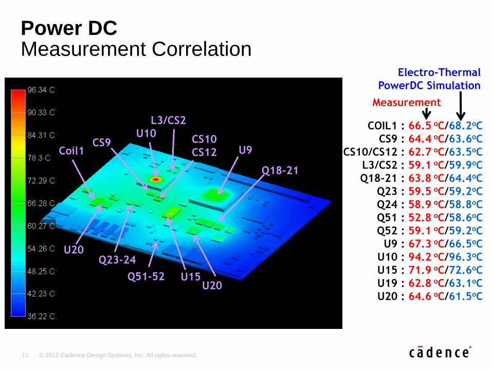
PowerDC Primary Advantages
The first and only integrated and automated electrical and thermal co-simulation for PCBs and packages
Patented time saving automation for remote sense line positioning
Fastest and most accurate IR drop solution
Broad range of visualization options for rapid design improvement
Unique block diagram results visualization supporting what-if updating
Power DC block diagram view
Current density & temperature

16 © 2012 Cadence Design Systems, Inc. All rights reserved.
PowerSI
PowerSI is an
advanced signal
integrity, power
integrity and design-
stage EMI solution.
Supports S-parameter
model extraction and
provides robust
frequency domain
simulation for entire
IC package and PCB
designs.

17 © 2012 Cadence Design Systems, Inc. All rights reserved.
PowerSI Virtual Network Analyzer Extracts N-port Impedance and S-parameters
Edward Chan et al, “High Speed DDR Performance in 4 vs 6 Layer FCBGA Package Design,” ECTC 2004
PowerSI

18 © 2012 Cadence Design Systems, Inc. All rights reserved.
Power SI Correlation of Simulated & Measured PDN
• Memory DIMM PCB
• Bare board w/ decaps
• PDN impedance measured PDS Simulation
Measurement
Log Scale
Linear Scale
red = vcc
green = ground
19 © 2012 Cadence Design Systems, Inc. All rights reserved.
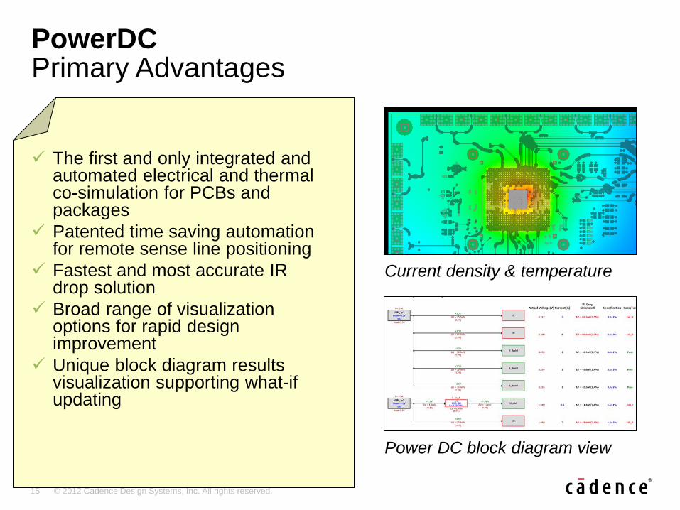
Power SI Broadband Model PI/SI Extraction
Only pwr/gnd may be
extracted or signals may also
be included.
Here, the S-parameters are
extracted for eight differential
pairs, plus their associated
pwr/gnd nets, from die-side
to BGA- side of a package.

20 © 2012 Cadence Design Systems, Inc. All rights reserved.
Power SI Source-free and Driven PDN Resonances are characterized
PDN Impedance Profile point-n-click probed at cursor location
3D display
2D display

21 © 2012 Cadence Design Systems, Inc. All rights reserved.
Measurements Hybrid Analysis
Power SI Near and Far fields through Postprocessing results after analysis Far Fields
FCC
Near Fields
Hot Spots
22 © 2012 Cadence Design Systems, Inc. All rights reserved.
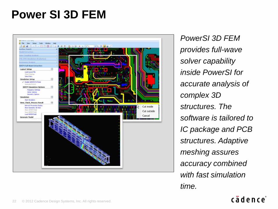
Power SI 3D FEM
PowerSI 3D FEM
provides full-wave
solver capability
inside PowerSI for
accurate analysis of
complex 3D
structures. The
software is tailored to
IC package and PCB
structures. Adaptive
meshing assures
accuracy combined
with fast simulation
time.
23 © 2012 Cadence Design Systems, Inc. All rights reserved.
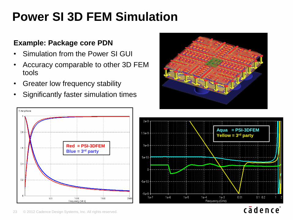
Power SI 3D FEM Simulation
Example: Package core PDN
• Simulation from the Power SI GUI
• Accuracy comparable to other 3D FEM tools
• Greater low frequency stability
• Significantly faster simulation times
Red = PSI-3DFEM
Blue = 3rd party
Aqua = PSI-3DFEM
Yellow = 3rd party
24 © 2012 Cadence Design Systems, Inc. All rights reserved.
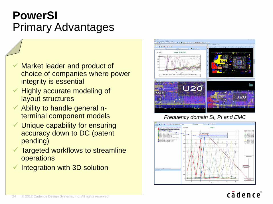
PowerSI Primary Advantages
Market leader and product of choice of companies where power integrity is essential
Highly accurate modeling of layout structures
Ability to handle general n-terminal component models
Unique capability for ensuring accuracy down to DC (patent pending)
Targeted workflows to streamline operations
Integration with 3D solution
Frequency domain SI, PI and EMC

25 © 2012 Cadence Design Systems, Inc. All rights reserved.
Optimize PI
OptimizePI is a highly
automated board and
IC Package AC
frequency analysis
solution. Supports
pre- and post-layout
decap studies and
identifies impedance
issues. Decap
implementations are
optimized for
performance and
cost

26 © 2012 Cadence Design Systems, Inc. All rights reserved.
• Device/VRM location and mounting
layer
• Locations and mounting layers of
decaps (top/bottom/under)
• Fanout from decaps
• Stackup and plane separation
• Voids on power and GND plane
VRM Device Device
Device
Device
VRM
U1
Optimize PI Explore design tradeoffs quickly

27 © 2012 Cadence Design Systems, Inc. All rights reserved.
Optimize PI Pre-route and Post-route optimization results for BOM and placement
Setup: 10 minutes
Simulation: 1 minute
Decap optimization: 6 minutes
Total pre-layout analysis time: 17 minutes
Optimization Objective:
Number of Decaps
39 decaps
$0.55
1st Optimization
Optimization Objective:
Cost
44 decaps
$0.42
2nd Optimization

28 © 2012 Cadence Design Systems, Inc. All rights reserved.
Optimize PI Example
Before
After
Decaps

29 © 2012 Cadence Design Systems, Inc. All rights reserved.
Optimize PI Validation of improved performance at lower cost in both time and frequency domain
Optimized Design
Original Design

30 © 2012 Cadence Design Systems, Inc. All rights reserved.
Optimize PI Quickly identify ineffective Decap locations with loop inductance analysis
Low Loop Inductance
High Loop
Inductance
Low Loop Inductance
31 © 2012 Cadence Design Systems, Inc. All rights reserved.
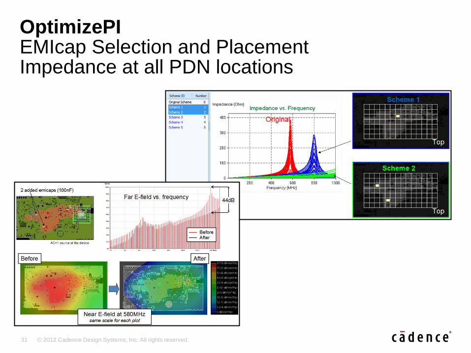
OptimizePI EMIcap Selection and Placement Impedance at all PDN locations

32 © 2012 Cadence Design Systems, Inc. All rights reserved.
OptimizePI Primary Advantages
Automated decap optimization and verification features
Clear presentation of economic benefits from decap optimization
Flexibility in meeting targeted objectives (performance, cost, area …)
Easy-to-use AC analysis environment.
Unique device impedance and EMI resonance checking
Support for early-stage studies and post-post layout verification
Automated positioning of EMI
decaps
33 © 2012 Cadence Design Systems, Inc. All rights reserved.
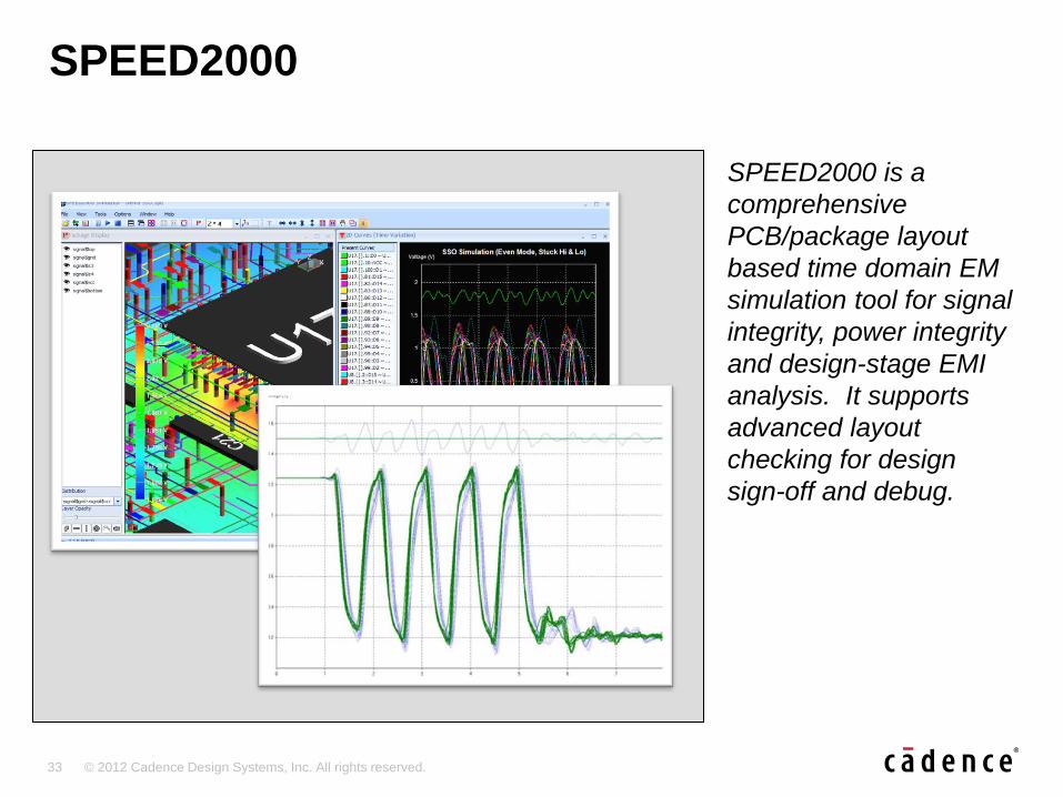
SPEED2000
SPEED2000 is a
comprehensive
PCB/package layout
based time domain EM
simulation tool for signal
integrity, power integrity
and design-stage EMI
analysis. It supports
advanced layout
checking for design
sign-off and debug.

34 © 2012 Cadence Design Systems, Inc. All rights reserved.
SPEED2000 Primary advantages
Unique animation of transient field propagation across PCBs and packages
Exceptional layout based signal integrity simulation including non-ideal power and ground systems
Only solution for EMC simulation with non-linear drivers and receivers
Customized workflows for layout electrical performance checks
Streamlined layout based DDR SSO simulation support
Trace coupling check
(initial and expanded views)
35 © 2012 Cadence Design Systems, Inc. All rights reserved.
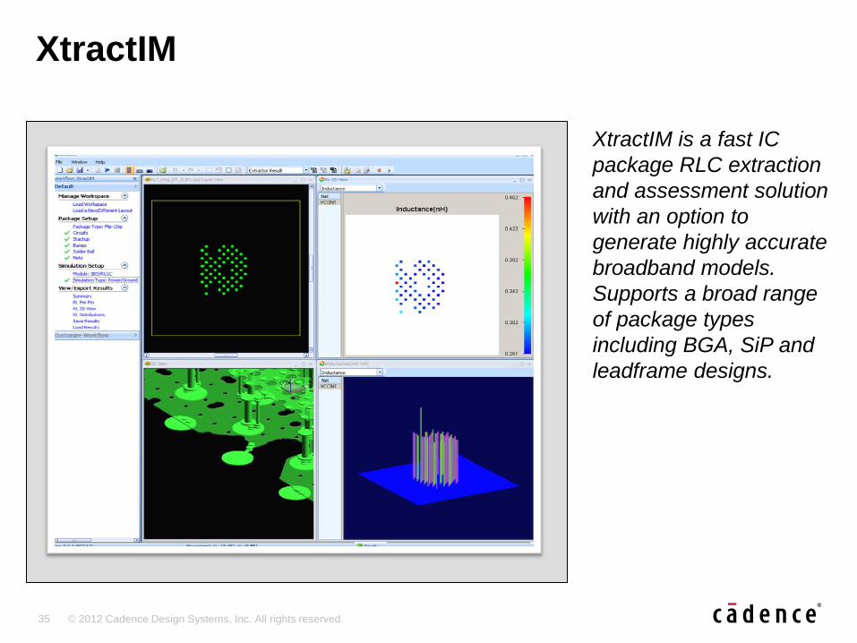
XtractIM
XtractIM is a fast IC
package RLC extraction
and assessment solution
with an option to
generate highly accurate
broadband models.
Supports a broad range
of package types
including BGA, SiP and
leadframe designs.

36 © 2012 Cadence Design Systems, Inc. All rights reserved.
XtractIM Primary Advantages
Built in package assessment rapidly identifies potential package defects
Unsurpassed extraction speed and ease of use
Able to address the broadest range of packages (single die & multi-die; flip chip, wirebond & leadframe)
Users control model extraction precision (RLCG to broadband accurate)
Easy to learn for occasional users and layout designers
HTML reports that can be readily shared with partners
Red curve shows impact off Per-pin self loop inductance

37 © 2012 Cadence Design Systems, Inc. All rights reserved.
Cadence Sigrity Products End-To-End System Level Analysis
SystemSI Modules for:
Serial Link Analysis and
Parallel Bus Analysis
Task focused signal
integrity solutions
primarily focused on
end-to-end interface
analysis (ex. DDR,
SerDes).
“Brocade became an early adopter of Cadence Sigrity’s SystemSI – Parallel Bus Analysis software,
which we use to perform rapid DDR3 simulations that accurately incorporate crucial power delivery
system impacts to ensure we can meet our tight timing margins.”
Shahriar Mokhatarzad
Brocade
June 1, 2011
System level analysis:
Die-to-Die high speed channels and buses

38 © 2012 Cadence Design Systems, Inc. All rights reserved.
SystemSI
SystemSI is a
comprehensive and
automated signal
integrity environment for
the accurate
assessment of high-
speed chip-to-chip
system designs.
Ensures robust parallel
bus and serial link
interface
implementations.
SystemSI – Serial Link Analysis
SystemSI – Parallel Bus Analysis

39 © 2012 Cadence Design Systems, Inc. All rights reserved.
SystemSI Primary Advantages
Fastest, most advanced channel simulation engine
Simplified model connections with Model Connection Protocol (MCP) and block-wise editor
Highly automated measurement and reporting capabilities
Unique AMI IP library for model generation
Clear linkage between schematic model and physical layout
Early studies supported with accurate 3D FEM based Via Wizard
Above = DDR / Below = Serial Link
40 © 2012 Cadence Design Systems, Inc. All rights reserved.
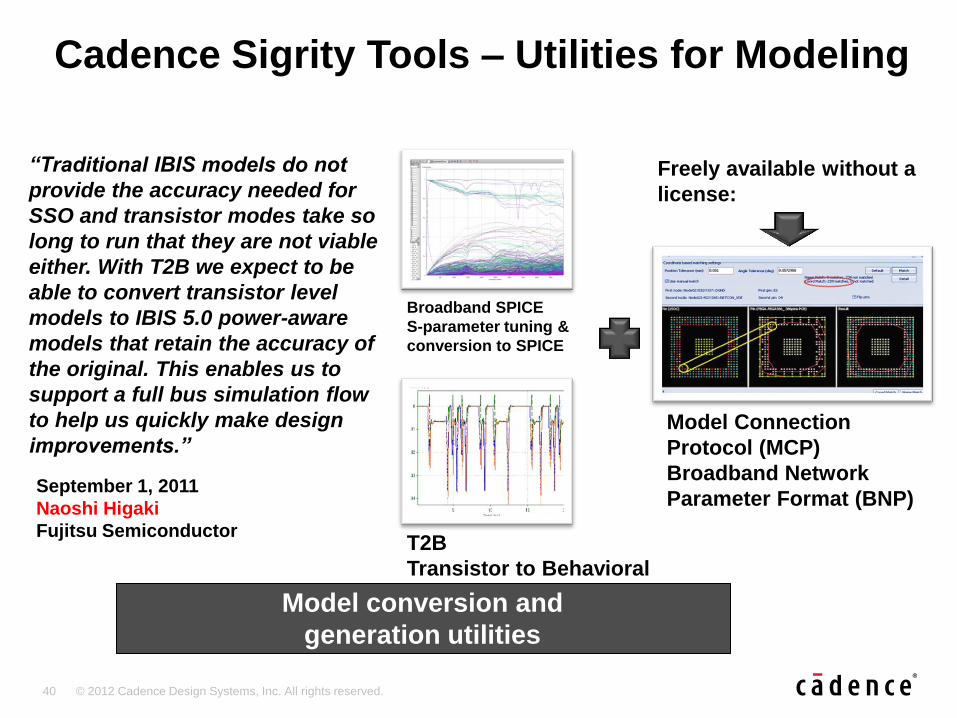
Cadence Sigrity Tools – Utilities for Modeling
Model Utilities
Freely available without a
license:
T2B
Transistor to Behavioral
Conversion
Broadband SPICE
S-parameter tuning &
conversion to SPICE
Model Connection
Protocol (MCP)
Broadband Network
Parameter Format (BNP)
“Traditional IBIS models do not
provide the accuracy needed for
SSO and transistor modes take so
long to run that they are not viable
either. With T2B we expect to be
able to convert transistor level
models to IBIS 5.0 power-aware
models that retain the accuracy of
the original. This enables us to
support a full bus simulation flow
to help us quickly make design
improvements.”
September 1, 2011
Naoshi Higaki
Fujitsu Semiconductor
Model conversion and
generation utilities

41 © 2012 Cadence Design Systems, Inc. All rights reserved.
Broadband SPICE
Broadband SPICE offers
a combination of S-
parameter checking,
tuning and extraction
capability to convert N-
port network parameters
to efficient SPICE
compatible circuits that
can be used in time
domain simulations.

42 © 2012 Cadence Design Systems, Inc. All rights reserved.
Broadband SPICE Primary Advantages
Market leader for micro-model extraction
Extensive checking functions for S-parameter model tuning and improvement
Automated adaptive port reference impedance technique to enhance model accuracy (patent pending)
Enables faster S-parameter simulations
Integration with PowerSI and SystemSI for streamlined design flows
Red curve shows impact off
S-parameter tuning

43 © 2012 Cadence Design Systems, Inc. All rights reserved.
T2B
Transistor to Behavioral
Model Conversion (T2B)
provides an efficient way
to create accurate
models for SSO and
other simulations.
These models run an
order of magnitude
faster than the original
transistor models.

44 © 2012 Cadence Design Systems, Inc. All rights reserved.
T2B Primary Advantages
Industry’s most advanced tool for converting transistor models to IBIS
Provides IBIS v5.0 power-aware model support
Cadence Sigrity’s IBIS plus model provides even more accuracy
Convenient GUI verifies conversion accuracy
Makes full bus simulations practical that would take weeks otherwise
Exceptional field support worldwide
Impact of pre-driver current
Built-in simulation check
compares transistor to IBIS
power-aware model

45 © 2012 Cadence Design Systems, Inc. All rights reserved.
MCP
Model Connection
Protocol (MCP)
simplifies time
consuming model
connections to support
multi-structure
simulations. Tedious
and error prone
operations are
streamlined to make
complex simulations
practical.
46 © 2012 Cadence Design Systems, Inc. All rights reserved.
MCP Primary Advantages
Open format, available from
Cadence Sigrity without charge
Simplifies connections to enable
multi-structure simulations
Reduces error-prone connection
tasks
Makes in practical to predict
localized behavior by enabling
per-pin connections
Used by Cadence Sigrity,
Synopsys and others
Simplified model connections

47 © 2012 Cadence Design Systems, Inc. All rights reserved.
Chip
analysis:
Power / IO
Cadence Sigrity Products Chip Level Analysis
XcitePI Modules for:
Planning
Extraction (Core / IO)
Co-simulation (FD / TD)
Chip model
extraction and
analysis.
“Cadence Sigrity’s electromagnetic analysis tool suite offers excellent accuracy and the company’s
expertise is especially valuable in tackling challenges associated with 2.5D and 3D IC designs.”
Suk Lee
TSMC, June 1, 2011

48 © 2012 Cadence Design Systems, Inc. All rights reserved.
XcitePI
XcitePI is a full-chip
power integrity
solution targeting on
chip / system co-
design applications. It
supports early chip
power planning, IO
and core model
extraction, and
simulation in both the
time and frequency
domains.

49 © 2012 Cadence Design Systems, Inc. All rights reserved.
XcitePI Primary Advantages
Performs both transient and frequency domain analysis of on-die PDN including packaging effects
Easy what-if analysis of decoupling capacitor placement, and power grid and bump design changes
Generates full-chip PDN models with high pin resolution and compact circuit size
Quickly checks IO power/ground and signal electrical performance to identify potential design defects
Generates IO power/ground and signal interconnect models for system-level analysis of high-speed channels and buses
Supports early stage studies and post-layout verification
Power net self loop inductance at each IO cell
Power net impedance
(L = power net only / R = power net plus on-die circuit

50 © 2012 Cadence Design Systems, Inc. All rights reserved.
Sigrity Analysis Tool Bundles
• SIGR201 PowerDC
• SIGR301 PowerSI
• SIGR311 3D-EM
• SIGR051 OptimizePI
• SIGR031 CAD Translators
Power Integrity
Note: Each bundle is a single user license. Only one of the products listed in each bundle can be run at a time.
• SIGR556 SystemSI – PBA
• SIGR301 PowerSI
• SIGR311 3D-EM
• SIGR400 SPEED2000
• SIGR021 T2B
• SIGR011 Broadband SPICE
• SIGR031 CAD Translators
Power-Aware SI
• SIGR506 SystemSI – SLA
• SIGR301 PowerSI
• SIGR311 3D-EM
• SIGR021 T2B
• SIGR011 Broadband SPICE
• SIGR031 CAD Translators
Serial Link SI
• SIGR801 XtractIM
• SIGR201 PowerDC
• SIGR311 3D-EM
• SIGR031 CAD Translators
Package Extraction

51 © 2012 Cadence Design Systems, Inc. All rights reserved.
Allegro Sigrity SI Base product enables constraint-driven design
− Options for detailed analysis, compliance and assessment
Allegro Sigrity SI – Base + Options
Allegro Sigrity SI (Base) Layout floorplanning/editing, schematic-level topology exploration and TD SI simulation,
constraint development/capture, analysis model library management, design translators … SI related ERCs
Packag
e A
ss
ess
men
t
an
d E
xtr
acti
on
Op
tio
n
Seri
al
Lin
k A
naly
sis
Op
tio
n
Po
wer-
Aw
are
SI O
pti
on
Allegro Sigrity SI
Base + Options
availability occurred
early Q1 2013

52 © 2012 Cadence Design Systems, Inc. All rights reserved.
Sig
no
ff A
naly
sis
an
d
Op
tim
izati
on
Op
tio
n
• Allegro Sigrity PI Base product
• enables basic DC Analysis and decap selection/placement guidance with “in-design” access
• Power Integrity analysis option – Signoff and Optimization option provides detailed verification of DC and AC
PDN performance and optimization of decap values and placement
Futu
re O
ptions …
Allegro Sigrity PI (Base)
Layout floorplanning/editing, analysis model library management, design translators,
PI related ERCs (screening) and first order(fast) AC/DC PI analysis
Pack
ag
e A
ssessm
en
t
an
d E
xtr
ac
tio
n O
pti
on
Allegro Sigrity PI
Base + Options
availability planned
late Q3 2013
Allegro Sigrity PI – Base + Options

53 © 2012 Cadence Design Systems, Inc. All rights reserved.
Summary
Cadence and Sigrity
− best-in-class stand-alone solutions, even better together
− ASI integration progressing quickly
Sigrity PI tools bundle addresses all DC and AC PI analysis needs
− upgrade path to ASI Base + Options
ASI PI Base + Options solution
− will provide the industry’s first constraint-driven PI flow
− enables design engineers to put the right decaps into the schematic, associated with the right ICs
− enables layout designers to address IR drop issues in-design
− enables PI engineer to move their value-add upstream in the design process (and sign off on much higher quality PDN designs)

54 © 2012 Cadence Design Systems, Inc. All rights reserved.


![SECURITIES AND EXCHANGE COMMISSION Integrity Life ... · SECURITIES AND EXCHANGE COMMISSION [Release Number IC-27677; File No. 812-13321] Integrity Life Insurance Company, et al.](https://static.fdocuments.in/doc/165x107/5f0a9ae47e708231d42c73e1/securities-and-exchange-commission-integrity-life-securities-and-exchange-commission.jpg)