
CACTI 5 - About HP Labs · CACTI 5.1 Shyamkumar Thoziyoor, Naveen Muralimanohar, Jung Ho Ahn, and...
75
CACTI 5.1 Shyamkumar Thoziyoor, Naveen Muralimanohar, Jung Ho Ahn, and Norman P. Jouppi HP Laboratories, Palo Alto HPL-2008-20 April 2, 2008* cache, memory, area, power, access time, DRAM CACTI 5.1 is a version of CACTI 5 fixing a number of small bugs in CACTI 5.0. CACTI 5 is the latest major revision of the CACTI tool for modeling the dynamic power, access time, area, and leakage power of caches and other memories. CACTI 5 includes a number of major improvements over CACTI 4. First, as fabrication technologies enter the deep-submicron era, device and process parameter scaling has become non-linear. To better model this, the base technology modeling in CACTI 5 has been changed from simple linear scaling of the original CACTI 0.8 micron technology to models based on the ITRS roadmap. Second, embedded DRAM technology has become available from some vendors, and there is interest in 3D stacking of commodity DRAM with modern chip multiprocessors. As another major enhancement, CACTI 5 adds modeling support of DRAM memories. Third, to support the significant technology modeling changes above and to enable fair comparisons of SRAM and DRAM technology, the CACTI code base has been extensively rewritten to become more modular. At the same time, various circuit assumptions have been updated to be more relevant to modern design practice. Finally, numerous bug fixes and small feature additions have been made. For example, the cache organization assumed by CACTI is now output graphically to assist users in understanding the output generated by CACTI. Internal Accession Date Only Approved for External Publication © Copyright 2008 Hewlett-Packard Development Company, L.P.
Transcript of CACTI 5 - About HP Labs · CACTI 5.1 Shyamkumar Thoziyoor, Naveen Muralimanohar, Jung Ho Ahn, and...

CACTI 5.1
Shyamkumar Thoziyoor, Naveen Muralimanohar, Jung Ho Ahn, and Norman P. Jouppi HP Laboratories, Palo Alto HPL-2008-20 April 2, 2008* cache, memory, area, power, access time, DRAM
CACTI 5.1 is a version of CACTI 5 fixing a number of small bugs in CACTI 5.0. CACTI 5 is the latest major revision of the CACTI tool for modeling the dynamic power, access time, area, and leakage power of caches and other memories. CACTI 5 includes a number of major improvements over CACTI 4. First, as fabrication technologies enter the deep-submicron era, device and process parameter scaling has become non-linear. To better model this, the base technology modeling in CACTI 5 has been changed from simple linear scaling of the original CACTI 0.8 micron technology to models based on the ITRS roadmap. Second, embedded DRAM technology has become available from some vendors, and there is interest in 3D stacking of commodity DRAM with modern chip multiprocessors. As another major enhancement, CACTI 5 adds modeling support of DRAM memories. Third, to support the significant technology modeling changes above and to enable fair comparisons of SRAM and DRAM technology, the CACTI code base has been extensively rewritten to become more modular. At the same time, various circuit assumptions have been updated to be more relevant to modern design practice. Finally, numerous bug fixes and small feature additions have been made. For example, the cache organization assumed by CACTI is now output graphically to assist users in understanding the output generated by CACTI.
Internal Accession Date Only Approved for External Publication
© Copyright 2008 Hewlett-Packard Development Company, L.P.

CACTI 5.1
Shyamkumar Thoziyoor, Naveen Muralimanohar, Jung Ho Ahn, and Norman P. [email protected], [email protected], [email protected], [email protected]
April 1, 2008
Abstract
CACTI 5.1 is a version of CACTI 5 fixing a number of small bugs inCACTI 5.0. CACTI 5 is the latest majorrevision of the CACTI tool for modeling the dynamic power, access time, area, and leakage power of caches and othermemories. CACTI 5 includes a number of major improvements over CACTI 4. First, as fabrication technologiesenter the deep-submicron era, device and process parameterscaling has become non-linear. To better model this, thebase technology modeling in CACTI 5 has been changed from simple linear scaling of the original CACTI 0.8 microntechnology to models based on the ITRS roadmap. Second, embedded DRAM technology has become available fromsome vendors, and there is interest in 3D stacking of commodity DRAM with modern chip multiprocessors. As anothermajor enhancement, CACTI 5 adds modeling support of DRAM memories. Third, to support the significant technologymodeling changes above and to enable fair comparisons of SRAM and DRAM technology, the CACTI code base hasbeen extensively rewritten to become more modular. At the same time, various circuit assumptions have been updatedto be more relevant to modern design practice. Finally, numerous bug fixes and small feature additions have been made.For example, the cache organization assumed by CACTI is now output graphically to assist users in understanding theoutput generated by CACTI.
1

Contents
1 Introduction 5
2 Changes and Enhancements in Version 5 52.1 Organizational Changes . . . . . . . . . . . . . . . . . . . . . . . . . . .. . . . . . . . . . . . . . . . 52.2 Circuit and Sizing Changes . . . . . . . . . . . . . . . . . . . . . . . . .. . . . . . . . . . . . . . . . 52.3 Technology Changes . . . . . . . . . . . . . . . . . . . . . . . . . . . . . . .. . . . . . . . . . . . . 62.4 DRAM Modeling . . . . . . . . . . . . . . . . . . . . . . . . . . . . . . . . . . . .. . . . . . . . . . 72.5 Miscellaneous Changes . . . . . . . . . . . . . . . . . . . . . . . . . . . .. . . . . . . . . . . . . . . 8
2.5.1 Optimization Function Change . . . . . . . . . . . . . . . . . . . .. . . . . . . . . . . . . . . 82.5.2 New Gate Area Model . . . . . . . . . . . . . . . . . . . . . . . . . . . . . .. . . . . . . . . 82.5.3 Wire Model . . . . . . . . . . . . . . . . . . . . . . . . . . . . . . . . . . . . .. . . . . . . . 82.5.4 ECC and Redundancy . . . . . . . . . . . . . . . . . . . . . . . . . . . . . .. . . . . . . . . 82.5.5 Display Changes . . . . . . . . . . . . . . . . . . . . . . . . . . . . . . . .. . . . . . . . . . 9
3 Data Array Organization 93.1 Mat Organization . . . . . . . . . . . . . . . . . . . . . . . . . . . . . . . . .. . . . . . . . . . . . . 103.2 Routing to Mats . . . . . . . . . . . . . . . . . . . . . . . . . . . . . . . . . . .. . . . . . . . . . . . 113.3 Organizational Parameters of a Data Array . . . . . . . . . . . .. . . . . . . . . . . . . . . . . . . . . 133.4 Comments about Organization of Data Array . . . . . . . . . . . .. . . . . . . . . . . . . . . . . . . 14
4 Circuit Models and Sizing 164.1 Wire Modeling . . . . . . . . . . . . . . . . . . . . . . . . . . . . . . . . . . . .. . . . . . . . . . . 164.2 Sizing Philosophy . . . . . . . . . . . . . . . . . . . . . . . . . . . . . . . .. . . . . . . . . . . . . . 174.3 Sizing of Mat Circuits . . . . . . . . . . . . . . . . . . . . . . . . . . . . .. . . . . . . . . . . . . . . 17
4.3.1 Predecoder and Decoder . . . . . . . . . . . . . . . . . . . . . . . . . .. . . . . . . . . . . . 174.3.2 Bitline Peripheral Circuitry . . . . . . . . . . . . . . . . . . . .. . . . . . . . . . . . . . . . . 19
4.4 Sense Amplifier Circuit Model . . . . . . . . . . . . . . . . . . . . . . .. . . . . . . . . . . . . . . . 214.5 Routing Networks . . . . . . . . . . . . . . . . . . . . . . . . . . . . . . . . .. . . . . . . . . . . . . 22
4.5.1 Array Edge to Bank Edge H-tree . . . . . . . . . . . . . . . . . . . . .. . . . . . . . . . . . . 224.5.2 Bank Edge to Mat H-tree . . . . . . . . . . . . . . . . . . . . . . . . . . .. . . . . . . . . . . 22
5 Area Modeling 235.1 Gate Area Model . . . . . . . . . . . . . . . . . . . . . . . . . . . . . . . . . . .. . . . . . . . . . . 245.2 Area Model Equations . . . . . . . . . . . . . . . . . . . . . . . . . . . . . .. . . . . . . . . . . . . 25
6 Delay Modeling 296.1 Access Time Equations . . . . . . . . . . . . . . . . . . . . . . . . . . . . .. . . . . . . . . . . . . . 306.2 Random Cycle Time Equations . . . . . . . . . . . . . . . . . . . . . . . .. . . . . . . . . . . . . . . 30
7 Power Modeling 317.1 Calculation of Dynamic Energy . . . . . . . . . . . . . . . . . . . . . .. . . . . . . . . . . . . . . . 31
7.1.1 Dynamic Energy Calculation Example for a CMOS Gate Stage . . . . . . . . . . . . . . . . . 317.1.2 Dynamic Energy Equations . . . . . . . . . . . . . . . . . . . . . . . .. . . . . . . . . . . . 32
7.2 Calculation of Leakage Power . . . . . . . . . . . . . . . . . . . . . . .. . . . . . . . . . . . . . . . 337.2.1 Leakage Power Calculation for CMOS gates . . . . . . . . . . .. . . . . . . . . . . . . . . . 337.2.2 Leakage Power Equations . . . . . . . . . . . . . . . . . . . . . . . . .. . . . . . . . . . . . 34
2

8 Technology Modeling 358.1 Devices . . . . . . . . . . . . . . . . . . . . . . . . . . . . . . . . . . . . . . . . .. . . . . . . . . . 358.2 Wires . . . . . . . . . . . . . . . . . . . . . . . . . . . . . . . . . . . . . . . . . . .. . . . . . . . . 378.3 Technology Exploration . . . . . . . . . . . . . . . . . . . . . . . . . . .. . . . . . . . . . . . . . . . 38
9 Embedded DRAM Modeling 389.1 Embedded DRAM Modeling Philosophy . . . . . . . . . . . . . . . . . .. . . . . . . . . . . . . . . . 38
9.1.1 Cell . . . . . . . . . . . . . . . . . . . . . . . . . . . . . . . . . . . . . . . . . .. . . . . . . 399.1.2 Destructive Readout and Writeback . . . . . . . . . . . . . . . .. . . . . . . . . . . . . . . . 399.1.3 Sense Amplifier Input Signal . . . . . . . . . . . . . . . . . . . . . .. . . . . . . . . . . . . . 399.1.4 Refresh . . . . . . . . . . . . . . . . . . . . . . . . . . . . . . . . . . . . . . .. . . . . . . . 399.1.5 Wordline Boosting . . . . . . . . . . . . . . . . . . . . . . . . . . . . . .. . . . . . . . . . . 39
9.2 DRAM Array Organization and Layout . . . . . . . . . . . . . . . . . .. . . . . . . . . . . . . . . . 409.2.1 Bitline Multiplexing . . . . . . . . . . . . . . . . . . . . . . . . . . .. . . . . . . . . . . . . 409.2.2 Reference Cells forVDD Precharge . . . . . . . . . . . . . . . . . . . . . . . . . . . . . . . . . 40
9.3 DRAM Timing Model . . . . . . . . . . . . . . . . . . . . . . . . . . . . . . . . .. . . . . . . . . . 409.3.1 Bitline Model . . . . . . . . . . . . . . . . . . . . . . . . . . . . . . . . . .. . . . . . . . . . 409.3.2 Multisubbank Interleave Cycle Time . . . . . . . . . . . . . . .. . . . . . . . . . . . . . . . . 429.3.3 Retention Time and Refresh Period . . . . . . . . . . . . . . . . .. . . . . . . . . . . . . . . 42
9.4 DRAM Power Model . . . . . . . . . . . . . . . . . . . . . . . . . . . . . . . . . .. . . . . . . . . . 439.4.1 Refresh Power . . . . . . . . . . . . . . . . . . . . . . . . . . . . . . . . . .. . . . . . . . . 43
9.5 DRAM Area Model . . . . . . . . . . . . . . . . . . . . . . . . . . . . . . . . . . .. . . . . . . . . . 439.5.1 Area of Reference Cells . . . . . . . . . . . . . . . . . . . . . . . . . .. . . . . . . . . . . . 439.5.2 Area of Refresh Circuitry . . . . . . . . . . . . . . . . . . . . . . . .. . . . . . . . . . . . . . 43
9.6 DRAM Technology Modeling . . . . . . . . . . . . . . . . . . . . . . . . . .. . . . . . . . . . . . . 449.6.1 Cell Characteristics . . . . . . . . . . . . . . . . . . . . . . . . . . .. . . . . . . . . . . . . . 44
10 Cache Modeling 4510.1 Organization . . . . . . . . . . . . . . . . . . . . . . . . . . . . . . . . . . .. . . . . . . . . . . . . . 4510.2 Delay Model . . . . . . . . . . . . . . . . . . . . . . . . . . . . . . . . . . . . .. . . . . . . . . . . 4610.3 Area Model . . . . . . . . . . . . . . . . . . . . . . . . . . . . . . . . . . . . . .. . . . . . . . . . . 4710.4 Power Model . . . . . . . . . . . . . . . . . . . . . . . . . . . . . . . . . . . . .. . . . . . . . . . . 47
11 Quantitative Evaluation 4711.1 Evaluation of New CACTI 5 Features . . . . . . . . . . . . . . . . . .. . . . . . . . . . . . . . . . . 47
11.1.1 Impact of New CACTI Solution Optimization . . . . . . . . .. . . . . . . . . . . . . . . . . . 4811.1.2 Impact of Device Technology . . . . . . . . . . . . . . . . . . . . .. . . . . . . . . . . . . . 4911.1.3 Impact of Interconnect Technology . . . . . . . . . . . . . . .. . . . . . . . . . . . . . . . . 5211.1.4 Impact of RAM Cell Technology . . . . . . . . . . . . . . . . . . . .. . . . . . . . . . . . . 53
11.2 Version 4.2 vs Version 5.1 Comparisons . . . . . . . . . . . . . .. . . . . . . . . . . . . . . . . . . . 55
12 Validation 6112.1 Sun SPARC 90nm L2 cache . . . . . . . . . . . . . . . . . . . . . . . . . . . .. . . . . . . . . . . . 6112.2 Intel Xeon 65nm L3 cache . . . . . . . . . . . . . . . . . . . . . . . . . . .. . . . . . . . . . . . . . 61
13 Commodity DRAM Technology and Main Memory Chip Modeling 65
14 Future Work 66
15 Conclusions 67
A Additional CACTI Validation Results for 90nm SPARC L2 68
3

B Additional CACTI Validation Results for 65 nm Xeon L3 71
4

1 Introduction
CACTI 5 is the latest major revision of the CACTI tool [30, 38,40, 47] for modeling the dynamic power, access time,area, and leakage power of caches and other memories. CACTI 5.1 is a version of CACTI 5 fixing a number of smallbugs in CACTI 5.0. CACTI has become widely used by computer architects, both directly and indirectly through othertools such as Wattch.
CACTI 5 includes a number of major improvements over CACTI 4.0. First, as fabrication technologies enter thedeep-submicron era, device and process parameter scaling has become non-linear. To better model this, the base technol-ogy modeling in CACTI 5 has been changed from simple linear scaling of the original 0.8 micron technology to modelsbased on the ITRS roadmap. Second, embedded DRAM technologyhas become available from some vendors, and thereis interest in 3D stacking of commodity DRAM with modern chipmultiprocessors. As another major enhancement,CACTI 5 adds modeling support of DRAM memories. Third, to support the significant technology modeling changesabove and to enable fair comparisons of SRAM and DRAM technology, the CACTI code base has been extensivelyrewritten to become more modular. At the same time, various circuit assumptions have been updated to be more rel-evant to modern design practice. Finally, numerous bug fixesand small feature improvements have been made. Forexample, the cache organization assumed by CACTI is now output graphically by the web-based server, to assist usersin understanding the output generated by CACTI.
The following section gives an overview of these changes, after which they are discussed in detail in subsequentsections.
2 Changes and Enhancements in Version 5
2.1 Organizational Changes
Earlier versions of CACTI (up to version 3.2) made use of a single row predecoder at the center of a memory bank withthe row predecoded signals being driven to the subarrays fordecoding. In version 4.0, this centralized decoding logicwas implicitly replaced with distributed decoding logic. Using H-tree distribution, the address bits were transmitted tothe distributed sinks where the decoding took place. However, because of some inconsistencies in the modeling, it wasnot clear at what granularity the distributed decoding tookplace - whether there was one sink per subarray or 2 or 4subarrays. There were some other problems with the CACTI code such as the following:
• The area model was not updated after version 3.2, so the impact on area of moving from centralized to distributeddecoding was not captured. Also, the leakage model did not account for the multiple distributed sinks. The impactof cache access type (normal/sequential/fast) [40] on areawas also not captured;
• Number of address bits routed to the subarrays was being computed incorrectly;
• Gate load seen by NAND gate in the 3-8 decode block was being computed incorrectly; and
• There were problems with the logic computing the degree of muxing at the tristate subarray output drivers.
In version 5, we resolve these issues, redefine and clarify what the organizational assumptions of memory are andremove ambiguity from the modeling. Details about the organization of memory can be found in Section 3.
2.2 Circuit and Sizing Changes
Earlier versions of CACTI made use of row decoding logic withtwo stages - the first stage was composed of 3-8predecode blocks (composed of NAND3 gates) followed by a NORdecode gate and wordline driver. The number ofgates in the row decoding path was kept fixed and the gates werethen sized using the method of logical effort [39] foran effective fanout of 3 per stage. In version 5, in addition to the row decoding logic, we also model the bitline muxdecoding logic and the sense-amplifier mux decoding logic. We use the same circuit structures to model all decodinglogic and we base the modeling on the effort described in [3].We use the sizing heuristic described in [3] that has beenshown to be good from an energy-delay perspective. With the new circuit structures and modeling that we use, the limit
5

on maximum number of signals that can be decoded is increasedfrom 4096 (in version 4.2) to 262144 (in version 5).While we do not expect the number of signals that are decoded to be very high, extending the limit from 4096 helpswith exploring area/delay/power tradeoffs in a more thorough manner for large memories, especially for large DRAMs.Details of the modeling of decoding logic are described in Section 4.
There are certain problems with the modeling of the H-tree distribution network in version 4.2. An inverter-driveris placed at branches of the address, datain, and dataout H-tree. However, the dataout H-tree does not model tristatedrivers. The output data bits may come from a few subarrays and so the address needs to be distributed to a fewsubarrays, however, dynamic power spent in transmitting address is computed as if all the data comes from a singlesubarray. The leakage in the drivers of the datain H-tree is not modeled.
In version 5, we model the H-tree distribution network more rigorously. For the dataout H-tree we model tristatebuffers at each branch. For the address and datain H-trees, instead of assuming inverters at the branches of the H-tree weassume the use of buffers that may be gated to allow or disallow the passage of signals and thereby control the dynamicpower. We size these drivers based on the methodology described in [3] which takes the resistance and capacitance ofintermediate wires into account during sizing. We also model the use of repeaters in the H-tree distribution networkwhich are sized according to equations from [11].
2.3 Technology Changes
Earlier versions of CACTI relied on a complicated way of obtaining device data for the input technology-node. Com-putation of access/cycle time and dynamic power were based off device data of a 0.8-micron process that was scaled tothe given technology-node using simple linear scaling principles. Leakage power calculation, however, made use of Ioff(subthreshold leakage current) values that were based off device data obtained through BSIM3 parameter extractions.In version 4.2, BSIM3 extraction was carried out for a few select technology nodes (130/100/70nm); as a result leakagepower estimation was available only for these select technology nodes.
There are several problems with the above approach of obtaining device data. Using two sets of parameters, onefor computation of access/cycle time/dynamic power and another for leakage power, is a convoluted approach and ishard to maintain. Also, the approach of basing device parameter values off a 0.8-micron process is not a good onebecause of several reasons. Device scaling has become quitenon-linear in the deep-submicron era. Device performancetargets can no longer be achieved through simple linear scaling of device parameters. Moreover, it is well-known thatphysical gate-lengths (according to the ITRS, physical gate-length is the final, as-etched length of the bottom of the gateelectrode) have scaled much more aggressively [4, 35] than what would be projected by simple linear scaling from the0.8 micron process.
In version 5, we adopt a simpler, more evolvable approach of obtaining device data. We use device data that theITRS [35] uses to make its projections. The ITRS makes use of the MASTAR software tool (Model for Assessmentof CMOS Technologies and Roadmaps) [36] for computation of device characteristics of current and future technologynodes. Using MASTAR, device parameters may be obtained for different technologies such as planar bulk, double gateand Silicon-On-Insulator. MASTAR includes device profile and result files of each year/technology-node for which theITRS makes projections and we incorporate the data from these files into CACTI. These device profiles are based offpublished industry process data and industry-consensus targets set by historical trends and system drivers. While it is notnecessary that these device numbers match or would match process numbers of various vendors in an exact manner, theydo come within the same ball-park as can be seen by looking at the Ion-Ioff cloud graphic within the MASTAR softwarewhich shows a scatter plot of various published vendor Ion-Ioff numbers and corresponding ITRS projections. Withthis approach of using device data from the ITRS, it also becomes possible to incorporate device data correspondingto different device types that the ITRS defines such as high performance (HP), LSTP (Low Standby Power), and LowOperating Power (LOP). More details about the device data used in CACTI can be found in Section 8.
There are some problems with interconnect modeling of version 4.2 also. Version 4.2 utilizes 2 types of wires in thedelay model, ‘local’ and ‘global’. The local type is used forwordlines and bitlines, while the global type is used for allother wires. The resistance per unit length and capacitanceper unit length for these two wire types are also calculated ina convoluted manner. For a given technology, the resistanceper unit length of the local wire is calculated by assumingideal scaling in all dimensions and using base data of a 0.8-micron process. The base resistance per unit length forthe 0.8-micron process is itself calculated by assuming copper wires in the base 0.8-micron process and readjusting the
6

sheet resistance value of version 3.2 which assumed aluminium wires. As the resistivity of copper is about 2/3rd that ofaluminium, the sheet resistance of copper was computed to be2/3rd that of aluminium. However, this implies that thethickness of metal assumed in versions 3.2 and 4.2 are the same which turns out to be not true. When we compute sheetresistance for the 0.8-micron process with the thickness oflocal wire assumed in version 4.2 and assuming a resistivityof 2.2 µohm-cm for copper, the value comes out to be a factor of 3.4 smaller than that used in version 3.2. In version4.2, resistance per unit length for the global wire type is calculated to be smaller than that of local wire type by a factorof 2.04. This factor of 2.04 is calculated based on RC delays and wire sizes of different wire types in the 2004 ITRSbut the underlying assumptions are not known. Another problem is that even though the delay model makes use of twotypes of wires, local and global, the area model makes use of just the local wire type and the pitch calculation of allwires (local type and global type) are based off the assumed width and spacing for the local wire type; this results in anunderestimation of pitch (and area) occupied by the global wires.
Capacitance per unit length calculation of version 4.2 alsosuffers from certain problems. The capacitance per unitlength values for local and global wire types are assumed to remain constant across technology nodes. The capacitanceper unit length value for local wire type was calculated for a65nm process as (2.9/3.6)*230 = 185 fF/m where 230 isthe published capacitance per unit length value for an Intel130nm process [42], 3.6 is the dielectric constant of the 130nm process and 2.9 is the dielectric constant of an Intel 65nmprocess [4]. Computing the value of capacitance per unitlength in this manner for a 65nm process ignores the fact thatthe fringing component of capacitance remains almostconstant across technology-nodes and scales very slowly [11, 31]. Also, assuming that the dielectric constant remainsfixed at 2.9 for future technology nodes ignores the possibility of use of lower-k dielectrics. Capacitance per unit lengthof the global type wire of version 4.2 is calculated to be smaller than that of local type wires by a factor of 1.4. Thisfactor of 1.4 is again calculated based on RC delays and wire sizes of different wire types in the 2004 ITRS but theunderlying assumptions again are not known.
In version 5, we remove the ambiguity from the interconnect modeling. We use the interconnect projections madein [11,13] which are based off well-documented simple models of resistance and capacitance. Because of the difficultyin projecting the values of interconnect properties in an exact manner at future technology nodes the approach employedin [11,13] was to come up with two sets of projections based onaggressive and conservative assumptions. The aggressiveprojections assume aggressive use of low-k dielectrics, insignificant resistance degradation due to dishing and scattering,and tall wire aspect ratios. The conservative projections assume limited use of low-k dielectrics, significant resistancedegradation due to dishing and scattering, and smaller wireaspect ratios. We incorporate both sets of projections intoCACTI. We also model 2 types of wires inside CACTI - semi-global and global with properties identical to that describedin [11, 13]. More details of the interconnect modeling are described in Section 8.2. Comparisons of area, delay, andpower of caches obtained using versions 4.2 and 5 are presented in Section 11.2.
2.4 DRAM Modeling
One of the major enhancements of version 5 is the incorporation of embedded DRAM models for a logic-based em-bedded DRAM fabrication process [19, 24, 27]. In the last fewyears, embedded DRAM has made its way into variousapplications. The IBM POWER4 made use of embedded DRAM in itsL3 cache [41]. The main compute chip insidethe Blue Gene/L supercomputer also makes use of embedded DRAM [14]. Embedded DRAM has also been used in thegraphics synthesizer unit of Sony’s PlayStation 2 [28].
In our modeling of embedded DRAM, we leverage the similaritythat exists in the global and peripheral circuitryof embedded SRAM and DRAM and model only their essential differences. We use the same array organization forembedded DRAM that we used for SRAM. By having a common framework that, in general, places embedded SRAMand DRAM on an equal footing and emphasizes only their essential differences, we are able to compare relative tradeoffsbetween embedded SRAM and DRAM. We describe the modeling of embedded DRAM in Section 9.
7

2.5 Miscellaneous Changes
2.5.1 Optimization Function Change
In version 5, we follow a different approach in finding the optimal solution with CACTI. Our new approach allows usersto exercise more control on area, delay, and power of the finalsolution. The optimization is carried out in the followingsteps: first, we find all solutions with area efficiency that iswithin a certain percentage (user-supplied value) of the areaefficiency of the solution with best area efficiency. We referto this area constraint asmax area constraint. Next,from this reduced set of solutions that satisfy themax area constraint, we find all solutions with access time that iswithin a certain percentage of the best access time solution(in the reduced set). We refer to this access time constraintasmax acc time constraint. To the subset of solutions that results after the application ofmax acc time constraint,we apply the following optimization function:
optimization-func =dynamic-energy
min-dynamic-energyflag-opt-for-dynamic-energy+
dynamic-powermin-dynamic-power
flag-opt-for-dynamic-power+
leak-powermin-leak-power
flag-opt-for-leak-power+
rand-cycle-timemin-rand-cycle-time
flag-opt-for-rand-cycle-time
where dynamic-energy, dynamic-power, leak-power, and rand-cycle-time are the dynamic energy, dynamic power,leakage power, and random cycle time of a solution respectively and min-dynamic-energy, min-dynamic-power, min-leak-power, and min-rand-cycle-time are their minimum (best) values in the subset of solutions being considered.flag-opt-for-dynamic-energy, flag-opt-for-dynamic-power, flag-opt-for-leak-power, and flag-opt-for-rand-cycle-time areuser-specified boolean variables. The new optimization process allows exploration of the solution space in a controlledmanner to arrive at a solution with user-desired characteristics.
2.5.2 New Gate Area Model
In version 5, we introduce a new analytical gate area model from [49]. With the new gate area model it becomes possibleto make the areas of gates sensitive to transistor sizing so that when transistor sizing changes, the areas also change. Withthe new gate area model, transistors may get folded when theyare subject to pitch-matching constraints and the areais calculated accordingly. This feature is useful in capturing differences in area caused due to different pitch-matchingconstraints that may have to be satisfied, particularly between SRAM and DRAM.
2.5.3 Wire Model
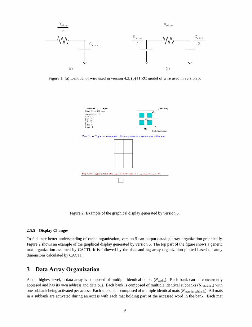
Version 4.2 models wires using the equivalent circuit modelshown in Figure 1(a). The Elmore delay of this model isRC/2, however this model underestimates the wire-to-gate component (RwireCgate) of delay. In version 5, we replace thismodel with theΠ RC model, shown in Figure 1(b), which has been used in more recent SRAM modeling efforts [2].
2.5.4 ECC and Redundancy
In order to be able to check and correct soft errors, most memories of today have support for ECC (Error CorrectionCode). In version 5, we capture the impact of ECC by incorporating a model that captures the ECC overhead in memorycell and data bus (datain and dataout) area. We incorporate avariable that specifies the number of data bits per ECC bit.By default, we fix the value of this variable to 8.
In order to improve yield, many memories of today incorporate redundant entities even at the subarray level. Forexample, the data array of the 16MB Intel Xeon L3 cache [7] which has 256 subarrays also incorporates 32 redundantsubarrays. In version 5, we incorporate a variable that specifies the number of mats per redundant mat. By default, wefix the value of this variable to 8.
8
Rwire
Cwire
2
(a)
Rwire
Cwire
Cwire
2 2
(b)
Figure 1: (a) L-model of wire used in version 4.2, (b)Π RC model of wire used in version 5.
Figure 2: Example of the graphical display generated by version 5.
2.5.5 Display Changes
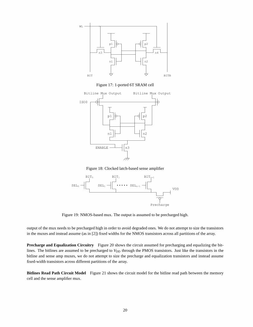
To facilitate better understanding of cache organization,version 5 can output data/tag array organization graphically.Figure 2 shows an example of the graphical display generatedby version 5. The top part of the figure shows a genericmat organization assumed by CACTI. It is followed by the dataand tag array organization plotted based on arraydimensions calculated by CACTI.
3 Data Array Organization
At the highest level, a data array is composed of multiple identical banks (Nbanks). Each bank can be concurrentlyaccessed and has its own address and data bus. Each bank is composed of multiple identical subbanks (Nsubbanks) withone subbank being activated per access. Each subbank is composed of multiple identical mats (Nmats-in-subbank). All matsin a subbank are activated during an access with each mat holding part of the accessed word in the bank. Each mat
9

BankSubbank
Mat
Array
Subarray
Figure 3: Layout of an example array with 4 banks. In this example each bank has 4 subbanks and each subbank has 4mats.
SubarraySubarray
Subarray Subarray
Predec
Logic
Figure 4: High-level composition of a mat.
itself is a self-contained memory structure composed of 4 identical subarrays and associated predecoding logic. Eachsubarray is a 2D matrix of memory cells and associated peripheral circuitry. Figure 3 shows the layout of an array with4 banks. In this example each bank is shown to have 4 subbanks and each subbbank is shown to have 4 mats. Not shownin Figure 3, address and data are assumed to be distributed tothe mats on H-tree distribution networks.
The rest of this section further describes details of the array organization assumed in CACTI. Section 3.1 describesthe organization of a mat. Section 3.2 describes the organization of the H-tree distribution networks. Section 3.3 presentsthe different organizational parameters associated with adata array.
3.1 Mat Organization
Figure 4 shows the high-level composition of all mats. A mat is always composed of 4 subarrays and associatedpredecoding/decoding logic which is located at the center of the mat. The predecoding/decoding logic is shared by all4 subarrays. The bottom subarrays are mirror images of the top subarrays and the left hand side subarrays are mirrorimages of the right hand side ones. Not shown in this figure, bydefault, address/datain/dataout signals are assumed toenter the mat in the middle through its sides; alternatively, under user-control, it may also be specified to assume thatthey traverse over the memory cells.
Figure 5 shows the high-level composition of a subarray. Thesubarray consists of a 2D matrix of the memory cellsand associated peripheral circuitry. Figure 6 shows the peripheral circuitry associated with bitlines of a subarray. Aftera wordline gets activated, memory cell data get transferredto bitlines. The bitline data may go through a level of bitlinemultiplexing before it is sensed by the sense amplifiers. Depending on the degree of bitline multiplexing, a single senseamplifier may be shared by multiple bitlines. The data is sensed by the sense amplifiers and then passed to tristate output
10

2D array
of memory cells
Sense Amplifier Mux
Subarray Output Drivers
Bitline Mux
Sense Amplifiers
Write Mux and Drivers
Precharge and Equalization
WordlineDrivers
Row Decode Gates
Figure 5: High-level composition of a subarray.
drivers which drive the dataout vertical H-tree (describedlater in this section). An additional level of multiplexingmaybe required at the outputs of the sense amplifiers in organizations in which the bitline multiplexing is not sufficient tocull out the output data or in set-associative caches in which the output word from the correct way needs to be selected.The select signals that control the multiplexing of the bitline mux and the sense amp mux are generated by the bitlinemux select signals decoder and the sense amp mux select signals decoder respectively. When the degree of multiplexingafter the outputs of the sense amplifiers is simply equal to the associativity of the cache, the sense amp mux select signaldecoder does not have to decode any address bits and instead simply buffers the input way-select signals that arrive fromthe tag array.
3.2 Routing to Mats
Address and data are routed to and from the mats on H-tree distribution networks. H-tree distribution networks are usedto route address and data and provide uniform access to all the mats in a large memory.1 Such a memory organizationis interconnect-centric and is well-suited for coping withthe trend of worsening wire delay with respect to device delay.Rather than shipping a bunch of predecoded address signals to the mats, it makes sense to ship the address bits anddecode them at the sinks (mats) [34]. Contemporary divided wordline architectures which make use of broadcast ofglobal signals suffer from increased wire delay as memory capacities get larger [2]. Details of a memory organizationsimilar to what we have assumed may also be found in [1]. For ease of pipelining multiple accesses in the array, separaterequest and reply networks are assumed. The request networkcarries address and datain from the edge of the array tothe mats while the reply network carries dataout from the mats to the edge of the array. The structure of the request andreply networks is similar; here we discuss the high-level organization of the request network.
The request H-tree network is divided into two networks:
1. The H-tree network from the edge of the array to the edge of abank; and,
2. The H-tree network from the edge of the bank to the mats.
Figure 7 shows the layout of the request H-tree network between the array edge and the banks. Address and datainare routed to each bank on this H-tree network and enter each bank at the middle from one of its sides. The H-tree
1Non-uniform cache architectures (NUCA) are currently beyond the scope of CACTI 5 but may be supported by future versionsof CACTI.
11

Bitline
Mux
Select
Signal
Decoder
Prechg
& Eq
SRAM
cell
SRAM
cell
SRAM
cell
Senseamp
Mux
Select
Signal
Decoder
Sense
Amplifier
Prechg
& Eq
SRAM
cell
SRAM
cell
SRAM
cell
Prechg
& Eq
SRAM
cell
SRAM
cell
SRAM
cell
Prechg
& Eq
SRAM
cell
SRAM
cell
SRAM
cell
Tristated
Subarray
Output Driver
Sense
Amplifier
Dataout Bit
Figure 6: Peripheral circuitry associated with bitlines. Not shown in this figure, but the outputs of the muxes are assumedto be precharged high.
Figure 7: Layout of edge of array to banks H-tree network.
network from the edge of the bank to the mats is further divided into two 1-dimensional horizontal and vertical H-treenetworks. Figure 8 shows the layout of the horizontal H-treewithin a bank which is located at the middle of the bankwhile Figure 9 shows the layout of the vertical H-trees within a bank. The leaves of the horizontal H-tree act as theparent nodes (marked as V0) of the vertical H-trees. In orderto understand the routing of signals on the H-tree networkswithin a bank, we use an illustrative example. Consider a bank with the following parameters: 1MB capacity, 256-bit
12

H1
H2
V0
H2
H0
V0V0 V0
Horizontal
H-tree
Figure 8: Layout of the horizontal H-tree within a bank.
output word, 4 subbanks, 4 mats in each subbank. Looked at together, Figures 8 and 9 can be considered to be thehorizontal and vertical H-trees within such a bank. The number of address bits required to address a word in this bankis 15. As there are 4 subbanks and because each mat in a subbankis activated during an access, the number of addressbits that need to be distributed to each mat is 13. Because each mat in a subbank produces 64 out of the 256 output bits,the number of datain signals that need to be distributed to each mat is 64. Thus 15 bits of address and 256 bits of datainenter the bank from the left side driven by the H0 node. At the H1 node, the 15 address signals are redriven such thateach of the two nodes H1 receive the 15 address signals. The datain signals split at node H1 and 128 datain signals goto the left H2 node and the other 128 go to the right H2 node. At each H2 node, the address signals are again redrivensuch that all of the 4 V0 nodes end up receiving the 15 address bits. The datain signals again split at each H2 node sothat each V0 node ends up receiving 64 datain bits. These 15 address bits and 64 datain bits then traverse to each matalong the 4 vertical H-trees. In the vertical H-trees, address and datain may either be assumed to be broadcast to all matsor alternatively, it may be assumed that these signals are appropriately gated so that they are routed to just the correctsubbank that contains the data; by default, we assume the latter scenario.
The reply network H-trees are similar in principle to the request network H-trees. In case of the reply networkvertical H-trees, dataout bits from each mat of a subbank travel on the vertical H-trees to the middle of the bank wherethey sink into the reply network horizontal H-tree, and are carried to the edge of the bank.
3.3 Organizational Parameters of a Data Array
In order to calculate the optimal organization based on a given objective function, like earlier versions of CACTI [30,38,40,47], each bank is associated with partitioning parametersNdwl, Ndbl andNspd, whereNdwl = number of segments in abank wordline,Ndbl = number of segments in a bank bitline, andNspd = number of sets mapped to each bank wordline.
Unlike earlier versions of CACTI, in CACTI 5Nspd can take on fractional values less than one. This is useful for
13

V1
V2
V2
V1
V0
V2
V2
V1
V2
V2
V1
V0
V2
V2
V1
V2
V2
V1
V0
V2
V2
V1
V2
V2
V1
V0
V2
V2
Figure 9: Layout of the vertical H-trees within a bank.
small highly-associative caches with large line sizes. Without values ofNspd less than one, memory mats with hugeaspect ratios with only a few word lines but hundreds of bits per word line would be created. For a pure scratchpadmemory (not a cache),Nspd is used to vary the aspect ratio of the memory bank.
NsubbanksandNmats-in-subbankare related toNdwl andNdbl as follows:
Nsubbanks =Ndbl
2(1)
Nmats-in-subbank =Ndwl
2(2)
Figure 10 shows different partitions of the same bank. The partitioning parameters are labeled alongside. Table 1lists various organizational parameters associated with adata array.
3.4 Comments about Organization of Data Array
The cache organization chosen in the CACTI model is a compromise between many possible different cache organiza-tions. For example, in some organizations all the data bits could be read out of a single mat. This could reduce dynamicpower but increase routing requirements. On the other hand,organizations exist where all mats are activated on a re-quest and each produces part of the bits required. This obviously burns a lot of dynamic power, but has the smallestrouting requirements. CACTI chooses a middle ground, whereall the bits for a read come from a single subbank, butmultiple mats. Other more complicated organizations, in which predecoders are shared by two subarrays instead of four,or in which sense amplifiers are shared between top and bottomsubarrays, are also possible, however we try to model asimple common case in CACTI.
14

Nmats-in-subbank
= 2
Nsubbanks
= 2
Nspd
= 1
Ndbl
= 4
Ndwl
= 4
Nmats-in-subbank
= 4
Nsubbanks
= 1
Nspd
= 2
Ndbl
= 2
Ndwl
= 8
Nmats-in-subbank
= 4
Nsubbanks
= 2
Nspd
= 1
Ndbl
= 4
Ndwl
= 8
Figure 10: Different partitions of a bank.
Parameter Name Meaning Parameter Type
Nbanks Number of banks User inputNdwl Number of divisions in a bank wordline Degree of freedomNdbl Number of divisions in a bank bitline Degree of freedomNspd Number of sets mapped to a bank wordline Degree of freedomDbitline-mux Degree of muxing at bitlines Degree of freedomDsenseamp-mux Degree of muxing at sense amp outputs Degree of freedomNsubbanks Number of subbanks CalculatedNmats-in-subbank Number of mats in a subbank CalculatedNsubarr-rows Number of rows in a subarray CalculatedNsubarr-cols Number of columns in a subarray CalculatedNsubarr-senseamps Number of sense amplifiers in a subarray CalculatedNsubarr-out-drivers Number of output drivers in a subarray CalculatedNbank-addr-bits Number of address bits to a bank CalculatedNbank-datain-bits Number of datain bits to a mat CalculatedNbank-dataout-bits Number of dataout bits from a mat CalculatedNmat-addr-bits Number of address bits to a mat CalculatedNmat-datain-bits Number of datain bits to a mat CalculatedNmat-dataout-bits Number of dataout bits from a mat CalculatedNmat-way-select Number of way-select bits to a mat (for data array of cache)Calculated
Table 1: Organizational parameters of a data array.
15

Rwire
Cwire
Cwire
2 2
Figure 11: One-sectionΠ RC model that we have assumed for non-ideal wires.
ground
ground
Cbot
Cright
Ctop
Cleft
Figure 12: Capacitance model from [11].
4 Circuit Models and Sizing
In Section 3, the high-level organization of an array was described. In this section, we delve deeper into logic and circuitdesign of the different entities. We also present the techniques adopted for sizing different circuits. The rest of thissection is organized as follows: First, in Section 4.1, we describe the circuit model that we have assumed for wires. Nextin Section 4.2, we describe the general philosophy that we have adopted for sizing circuits. Next in Section 4.3, wedescribe the circuit models and sizing techniques for the different circuits within a mat, and in Section 4.5, we describethem for the circuits used in the different H-tree networks.
4.1 Wire Modeling
Wires are considered to belong to one of two types: ideal or non-ideal. Ideal wires are assumed to have zero resistanceand capacitance. Non-ideal wires are assumed to have finite resistance and capacitance and are modeled using a one-sectionΠ RC model shown in Figure 11. In this figure,Rwire andCwire for a wire of lengthLwire are given by thefollowing equations:
Rwire = LwireRunit-length-wire (3)
Cwire = LwireCunit-length-wire (4)
For computation ofRunit-length-wire andCunit-length-wire wires, we use the equations presented in [11, 13] which arereproduced below. Figure 12 shows the accompanying picturefor the capacitance model from [11].
Runit-length-wire = αscatterρ
(thickness−barrier−dishing)(width−2∗barrier)(5)
Cunit-length-wire = ε0(2Mεhorizthicknessspacing
+2εvertwidth
ILDthick)+ fringe(εhoriz,εvert) (6)
16

4.2 Sizing Philosophy
In general the sizing of circuits depends on various optimization goals: circuits may be sized for minimum delay,minimum energy-delay product, etc. CACTI’s goal is to modelsimple representative circuit sizing applicable to a broadrange of common applications. As in earlier SRAM modeling efforts [2, 3, 20], we have made extensive use of themethod of logical effort [39] in sizing different circuit blocks. Explanation of the method of logical effort may be foundin [39].
4.3 Sizing of Mat Circuits
As described earlier in Section 3.1, a mat is composed of entities such as the predecoding/decoding logic, memory cellarray, and bitline peripheral circuitry. We present circuits, models, and sizing techniques for these entities.
4.3.1 Predecoder and Decoder
As discussed in Section 2, new circuit structures have been adopted for the decoding logic. The same decoding logiccircuit structures are utilized for producing the row-decode signals and the select signals of the bitline and sense amplifiermuxes. In the discussion here, we focus on the row-decoding logic. In order to describe the circuit structures assumedwithin the different entities of the row-decoding logic, weuse an illustrative example. Figure 13 shows the structureof the row-decoding logic for a subarray with 1024 rows. The row-decoding logic is composed of two row-predecodeblocks and the row-decode gates and drivers. The row-predecode blocks are responsible for predecoding the addressbits and generating predecoded signals. The row-decode gates and drivers are responsible for decoding the predecodedoutputs and driving the wordline load. Each row-predecode block can predecode a maximum of 9 bits and has a 2-levellogic structure. With 1024 rows, the number of address bits required for row-decoding is 10. Figure 14 shows thestructure of each row predecode block for a subarray with 1024 rows. Each row predecode block is responsible forpredecoding 5 address bits and each of them generates 32 predecoded output bits. Each predecode block has two levels.The first level is composed of one 2-4 decode unit and one 3-8 decode unit. At the second level, the 4 outputs from the2-4 decode unit and the 8 outputs from the 3-8 decode unit are combined together using 32 NAND2 gates in order toproduce the 32 predecoded outputs. The 32 predecoded outputs from each predecode block are combined together usingthe 1024 NAND2 gates to generate the row decode signals.
Figure 15 shows the circuit paths in the decoding logic for the subarray with 1024 rows. One of the paths containsthe NAND2 of the 2-4 decode unit and the other contains the NAND3 gate of the 3-8 decode unit. Each path has 3 stagesin its path. The branching efforts at the outputs of the first two stages are also shown in the figure. The predecode outputwire is treated as a non-ideal wire with itsRpredec-out-wireandCpredec-out-wirecomputed using the following equations:
Rpredec-output-wire = Lpredec-output-wireRunit-length-wire (7)
Cpredec-output-wire = Lpredec-output-wireCunit-length-wire (8)
whereLpredec-output-wireis the maximum length amongst lengths of predecode output wires.The sizing of gates in each circuit path is calculated using the method of logical effort. In each of the 3 stages of
each circuit path, minimum-size transistors are assumed atthe input of the stage and each stage is sized independent ofeach other using the method of logical effort. While this is not optimal from a delay point of view, it is simpler to modeland has been found to be a good sizing heuristic from an energy-delay point of view [3].
In this example that we considered for decoding logic of a subarray with 1024 rows, there were two different circuitpaths, one involving the NAND2 gate and another involving the NAND3 gate. In the general case, when each predecodeblock decodes different number of address bits, a maximum offour circuit paths may exist. When the degree of decodingis low, some of the circuit blocks shown in Figure 13 may not berequired. For example, Figure 16 shows the decodinglogic for a subarray with 8 rows. In this case, the decoding logic simply involves a 3-8 decode unit as shown.
As mentioned before, the same circuit structures used within the row-decoding logic are also used for generating theselect signals of the bitline and sense amplifier muxes. However, unlike the row-decoding logic in which the NAND2decode gates and drivers are assumed to be placed on the side of subarray, the NAND2 decode gates and drivers are
17

0
1
1023
Row predecode
block 22
1
0
3
4
0
1
31
Row predecode
block 12
1
0
3
4
0
1
31
Wordline driverRow decode
gate
Figure 13: Structure of the row decoding logic for a subarraywith 1024 rows.
0
1
31
2-4
decoder
3-8
decoder
0
1
2
3
2-4 decoder
Figure 14: Structure of the row predecode block for a subarray with 1024 rows.
assumed to be placed at the center of the mat near their corresponding predecode blocks. Also, the resistance/capacitanceof the wires between the predecode blocks and the decode gates are not modeled and are assumed to be zero.
18

gnand3
Wpredec-fl0
gnand2 gnand2
Wwl0
beffort = 4
Rwordline
Cwordline /2
Wwl1 Wwln-1
beffort = 32
Wpredec-fl1
Wpredec-fln-1
Wpredec-sl0
Wpredec-sl1
Wpredec-sln-1
Cwordline /2
Rpredec-out-wire
Cpredic-out-wire /2
Cpredic-out-wire /2
gnand2
Wpredec-fl0
gnand2 gnand2
Wwl0
beffort = 8
Rwordline
Cwordline /2
Wwl1 Wwln-1
beffort = 32
Wpredec-fl1
Wpredec-fln-1
Wpredec-sl0
Wpredec-sl1
Wpredec-sln-1
Cwordline /2
Rpredec-out-wire
Cpredic-out-wire /2
Cpredic-out-wire /2
Figure 15: Row decoding logic circuit paths for a subarray with 1024 rows. One of the circuit paths contains the NAND2gate of the 2-4 decode unit while the other contains the NAND3gate of the 3-8 decode unit.
3-8
decoder
Figure 16: Structure of the row-decoding logic for a subarray with 8 rows. The row-decoding logic is simply composedof 8 decode gates and drivers.
4.3.2 Bitline Peripheral Circuitry
Memory Cell Figure 17 shows the circuit assumed for a 1-ported SRAM cell.The transistors of the SRAM cell aresized based on the widths specified in [14] and are presented in Section 8.
Sense Amplifier Figure 18 shows the circuit assumed for a sense amplifier - it’s a clocked latch-based sense amplifier.When the ENABLE signal is not activated, there is no flow of current through the transistors of the latch. Whenthe ENABLE signal is activated the sensing begins. The isolation transistors are responsible for isolating the highcapacitance of the bitlines from the sense amplifier nodes during the sensing operation. The small-signal circuit modeland analysis of this latch-based sense amplifier is presented in Section 4.4.
Bitline and Sense Amplifier Muxes Figure 19 shows the circuit assumed for the bitline and senseamplifier muxes.We assume that the mux is implemented using NMOS pass transistors. The use of NMOS transistors implies that the
19
BITBBIT
WL
n3
p1
n1 n2
p2
n4
Figure 17: 1-ported 6T SRAM cell
Bitline Mux Output
ENABLE
ISO0
p1
n1 n2
p2
n3
Bitline Mux Output
Figure 18: Clocked latch-based sense amplifier
SEL0
BIT0
SEL1
BIT1
SELn-1
BITn-1
VDD
Precharge
Figure 19: NMOS-based mux. The output is assumed to be precharged high.
output of the mux needs to be precharged high in order to avoiddegraded ones. We do not attempt to size the transistorsin the muxes and instead assume (as in [2]) fixed widths for theNMOS transistors across all partitions of the array.
Precharge and Equalization Circuitry Figure 20 shows the circuit assumed for precharging and equalizing the bit-lines. The bitlines are assumed to be precharged toVDD through the PMOS transistors. Just like the transistors in thebitline and sense amp muxes, we do not attempt to size the precharge and equalization transistors and instead assumefixed-width transistors across different partitions of thearray.
Bitlines Read Path Circuit Model Figure 21 shows the circuit model for the bitline read path between the memorycell and the sense amplifier mux.
20

PRE PRE
VDD VDD
EQ
BIT0 BITB0
PRECHARGE PRE PRE
VDD VDD
EQ
BIT1 BITB1
PRE PRE
VDD VDD
EQ
BITn-1 BITBn-1
Figure 20: Bitline precharge and equalization circuitry.
Rbitline
Rcell-acc
Rcell-pull-down
Cbitline
2
Cbitline
2
Cdrain-bit-mux
Cdrain-bit-mux
Rbit-mux
Cdrain-iso
Cdrain-iso
Csense
Cdrain-senseamp-mux
Riso
Figure 21: Circuit model of the bitline read path between theSRAM cell and the sense amplifier input.
4.4 Sense Amplifier Circuit Model
Figure 18 showed the clocked latch-based sense amplifier that we have assumed. [10] presents analysis of this circuitand equations for sensing delay under different assumptions. Figure 22 shows one of the small-signal models presentedin [10]. Use of this small-signal model is based on two assumptions:
1. Current has been flowing in the circuit for a sufficiently long time; and
2. The equilibrating device can be modeled as an ideal switch.
For the small-signal model of Figure 22, it has been shown that the delay of the sensing operation is given by thefollowing equation:
21

M3
M1 M2
M4
Rgm1·v2
gm2·v1
gm3·v2 gm4·v1
v2v1v1
v2
R CC
Figure 22: Small-signal model of the latch-based sense amplifier [10].
Tsense =Csense
Gmln(
VDD
Vsense) (9)
Gm = gmn+gmp (10)
Use of Equation 9 for calculation of sense amplifier delay requires that the values ofgmn (NMOS transconductance)andgmp (PMOS transconductance) be known. We assume that the transistors in the sense amplifier latch exhibit short-channel effects. For a transistor that exhibits short-channel effect, we use the following typical current equation [29] forcomputation of saturation current:
Idsat =µeff
2Cox
WL
(VGS−VTH)Vdsat (11)
Differentiating the above equation with respect toVGS gives the equation forgm of the transistor. It can be seen thatbecause of short-channel effect,gm comes out to be independent ofVGS.
gm =µeff
2Cox
WL
Vdsat (12)
4.5 Routing Networks
As described earlier in Section 3.2, address and data are routed to and from the mats on H-tree distribution networks.First address/data are routed on an H-tree from array edge tobank edge and then on another H-tree from bank edge tothe mats.
4.5.1 Array Edge to Bank Edge H-tree
Figure 7 showed the layout of H-tree distribution of addressand data between the array edge and the banks. ThisH-tree network is assumed to be composed of inverter-based repeaters. The sizing of the repeaters and the separationdistance between them is determined based on the formulae given in [11]. In order to allow for energy-delay tradeoffsin the repeater design, we introduce an user-controlled variable “maximum percentage of delay away from best repeatersolution” ormax repeater delay constraint in short. Amax repeater delay constraint of zero results in thebest delay repeater solution. For amax repeater delay constraint of 10%, the delay of the path is allowed to getworse by a maximum of 10% with respect to the best delay repeater solution by reducing the sizing and increasingthe separation distance. Thus, with themax repeater delay constraint, limited energy savings are possible at theexpense of delay.
4.5.2 Bank Edge to Mat H-tree
Figures 8 and 9 showed layout examples of horizontal and vertical H-trees within a bank, each with 3 nodes. We assumethat drivers are placed at each of the nodes of these H-trees.Figure 23 shows the circuit path and driver circuit structure
22

W0 W1 Wn-1
Rw0 Cw0 Rwn-1 Cwn-1Rw1 Cw1
CLoad
CLoad
Figure 23: Circuit path of address/datain H-trees within a bank.
ENB
Rw0 Cw0
From Sense
amplifier
Subarray
output driver
EN
CLoad
ENB
ENB
Rw1 Cw1
ENB
ENB
ENB
ENBRwn-1 Cwn-1
ENB
ENB
Figure 24: Circuit path of vertical dataout H-trees.
of the address/datain H-trees, and Figure 24 shows the circuit path and driver circuit structure of the vertical dataoutH-tree. In order to allow for signal-gating in the address/datain H-trees we consider multi-stage buffers with a 2-inputNAND gate as the input stage. The sizing and number of gates ateach node of the H-trees is computed using themethodology described in [3] which takes into account the resistance and capacitance of the intermediate wires in theH-tree.
One problem with the circuit paths of Figures 23 and 24 is thatthey start experiencing increased wire delays asthe wire lengths between the drivers start to get long. This also limits the maximum random cycle time that can beachieved for the array. So, as an alternative to modeling drivers only at H-tree branching nodes, we also consideran alternative model in which the H-tree circuit paths within a bank are composed of buffers at regular intervals (i.e.repeaters). With repeaters, the delay through the H-tree paths within a bank can be reduced at the expense of increasedpower consumption. Figure 25 shows the different types of buffer circuits that have been modeled in the H-tree path. Atthe branches of the H-tree, we again assume buffers with a NAND gate in the input stage in order to allow for signal-gating whereas in the H-tree segments between two nodes, we model inverter-based buffers. We again size these buffersaccording to the buffer sizing formulae given in [11]. Themax repeater delay constraint that was described inSection 4.5.1 is also used here to decide the sizing of the buffers and their separation distance so that delay in theseH-trees also may be traded off for potential energy savings.
5 Area Modeling
In this section, we describe the area model of a data array. InSection 5.1, we describe the area model that we have usedto find the areas of simple gates. We then present the equations of the area model in Section 5.2.
23

ENEN
EN
EN
Figure 25: Different types of buffer circuit stages that have been modeled in the H-trees within a bank.
5.1 Gate Area Model
A new area model has been used to estimate the areas of transistors and gates such as inverter, NAND, and NORgates. This area model is based off a layout model from [49] which describes a fast technique to estimate standard cellcharacteristics before the cells are actually laid out. Figure 26 illustrates the layout model that has been used in [49].Table 2 shows the process/technology input parameters required by this gate area model. For a thorough description ofthe technique, please refer to [49]. Gates with stacked transistors are assumed to have a layout similar to that describedin [47]. When a transistor width exceeds a certain maximum value (Hn-diff for NMOS andHp-diff for PMOS in Table2), the transistor is assumed to be folded. This maximum value can either be process-specific or context-specific. Anexample of when a context-specific width would be used is in case of memory sense amplifiers which typically have tobe laid out at a certain pitch.
Given the width of an NMOS transistor,Wbefore-folding, the number of folded transistors may be calculated as follows:
Nfolded-transistors = ⌈Wbefore-folding
Hn-diff⌉ (13)
The equation for total diffusion width ofNstacked transistors when they are not folded is given by the followingequation:
24

VDD rail
GND railDiffusion gap height
Transistor region height
Minimum Poly-
to-Poly spacingP-type
diffusion
region
N-type
diffusion
region
Contact width
Minimum Poly-to-
Contact spacing
Figure 26: Layout model assumed for gates [49].
Parameter name Meaning
Hn-diff Maximum height of n diffusion of a transistorHp-diff Maximum height of p diffusion for a transistorHgap-bet-same-diffs Minimum gap between diffusions of the same typeHgap-bet-opp-diffs Minimum gap between n and p diffusionsHpower-rail Height ofVDD (GND) power railWp Minimum width of poly (poly half-pitch or process feature size)Sp-p Minimum poly-to-poly spacingWc Contact widthSp-c Minimum poly-to-contact spacing
Table 2: Process/technology input parameters required by the gate area model.
total-diff-width = 2(Wc +2Sp-c)+NstackedWp +(Nstacked−1)Sp-p (14)
The equation for total diffusion width ofNstackedtransistors when they are folded is given by the following equation:
total-diff-width = Nfolded-transistors(2(Wc +2Sp-c)+NstackedWp +(Nstacked−1)Sp-p) (15)
Note that Equation 15 is a generalized form of the equations used for calculating diffusion width (for computation ofdrain capacitance) in the original CACTI report [47]. Earlier versions of CACTI assumed at most two folded transistors;in version 5, we allow the degree of folding to be greater than2 and make the associated layout and area models moregeneral. Note that drain capacitance calculation in version 5 makes use of equations similar to 14 and 15 for computationof diffusion width.
The height of a gate is calculated using the following equation:
Hgate= Hn-diff +Hp-diff +Hgap-bet-opp-diffs+2Hpower-rail (16)
5.2 Area Model Equations
The area of the data array is estimated based on the area occupied by a single bank and the area spent in routing addressand data to the banks. It is assumed that the area spent in routing address and data to the bank is decided by the pitch ofthe routed wires. Figures 27 and 28 show two example arrays with 8 and 16 banks respectively; we present equationsfor the calculation of the areas of these arrays.
25

0.25Pall-wires
0.5Pall-wires
Pall-wires
Wbank
Hbank
Figure 27: Supporting figure for example area calculation ofarray with 8 banks.
0.125Pall-wires
0.25Pall-wires
Wbank
Hbank
0.5Pall-wires
Pall-wires
Figure 28: Supporting figure for example area calculation ofarray with 16 banks.
Adata-arr = Hdata-arrWdata-arr (17)
The pitch of wires routed to the banks is given by the following equation:
Pall-wires = PwireNwires-routed-to-banks (18)
For the data array of Figure 27 with 8 banks, the relevant equations are as follows:
Wdata-arr = 4Wbank+Pall-wires+2Pall-wires
4(19)
Hdata-arr = 2Hbank+Pall-wires
2(20)
Nwires-routed-to-banks = 8(Nbank-addr-bits+Nbank-datain-bits+Nbank-dataout-bits+
Nway-select-signals) (21)
26

For the data array of Figure 28 with 16 banks, the relevant equations are as follows:
Wdata-arr = 4Wbank+Pall-wires
2+2
Pall-wires
8(22)
Hdata-arr = 4Hbank+Pall-wires+2Pall-wires
4(23)
Nwires-routed-to-banks = 16(Nbank-addr-bits+Nbank-datain-bits+Nbank-dataout-bits+
Nway-select-signals) (24)
The banks in a data array are assumed to be placed in such a way that the number of banks in the horizontal directionis always either equal to or twice the number of banks in the vertical direction. The height and width of a bank iscalculated by computing the area occupied by the mats and thearea occupied by the routing resources of the horizontaland vertical H-tree networks within a bank. We again use an example to illustrate the calculations. Figures 8 and 9showed the layouts of horizontal and vertical H-trees within a bank. The horizontal and vertical H-trees were eachshown to have three branching nodes (H0, H1, and H2; V0, V1, and V2). Combined together, these horizontal andvertical H-trees may be considered as H-trees within a bank with 4 subbanks and 4 mats in each subbank. We presentarea model equations for such a bank.
Abank = HbankWbank (25)
In version 5, as described in Section 4.5, for the H-trees within a bank we assume that drivers are placed eitheronly at the branching nodes of the H-trees or that there are buffers at regular intervals in the H-tree segments. Whendrivers are present only at the branching nodes of the vertical H-trees within a bank, we consider two alternative modelsin accounting for area overhead of the vertical H-trees. In the first model, we consider that wires of the vertical H-trees may traverse over memory cell area; in this case, the area overhead caused by the vertical H-trees is in terms ofarea occupied by drivers which are placed between the mats. In the second model, we do not assume that the wirestraverse over the memory cell area and instead assume that they occupy area besides the mats. The second model isalso applicable when there are buffers at regular intervalsin the H-tree segments. The equations that we present next forarea calculation of a bank assume the second model i.e. the wires of the vertical H-trees are assumed to not pass overthe memory cell area. The equations for area calculation under the assumption that the vertical H-tree wires go over thememory cell area are quite similar. For our example bank with4 subbanks and 4 mats in each subbank, the height ofthe bank is calculated to be equal to the sum of heights of all subbanks plus the height of the routing resources of thehorizontal H-tree.
Hbank = 4Hmat+Hhor-htree (26)
The width of the bank is calculated to be equal to the sum of widths of all mats in a subbank plus the width of therouting resources of the vertical H-trees.
Wbank = 4(Wmat+Wver-htree) (27)
The height of the horizontal H-tree is calculated as the height of the area occupied by the wires in the H-tree. Thesewires include the address, way-select, datain, and dataoutsignals. Figure 29 illustrates the layout that we assume forthewires of the horizontal H-tree. We assume that the wires are laid out using a single layer of metal. The height of the areaoccupied by the wires can be calculated simply by finding the total pitch of all wires in the horizontal H-tree. Figure 30illustrates the layout style assumed for the vertical H-tree wires, and is similar to that assumed for the horizontal H-treewires. Again the width of the area occupied by a vertical H-tree can be calculated by finding the total pitch of all wiresin the vertical H-tree.
27

addr-mat + way-select-mat +
datain + dataout
2 2
addr-mat + way-select-mat +
datain + dataout
addr-mat + way-select-mat +
datain + dataout
4 4
Figure 29: Layout assumed for wires of the horizontal H-treewithin a bank.
addr-mat +
datain-mat +
dataout-mat
addr-mat +
datain-mat +
dataout-mat
addr-mat +
datain-mat +
dataout-mat
Figure 30: Layout assumed for wires of the vertical H-tree within a bank.
row-predecode-output
Subarray Subarray
Subarray Subarray
addr-mat + way-select-mat + datain + dataout +
2 2 2 2
bit-mux-sel + senseamp-mux-sel + write-mux-sel
Figure 31: Layout of a mat.
Hhor-htree = Phor-htree-wires (28)
Wver-htree = Pver-htree-wires (29)
The height and width of a mat are estimated using the following equations. Figure 31 shows the layout of a mat andillustrates the assumptions made in the following equations. We assume that half of the address, way-select, datain, anddataout signals enter the mat from its left and the other halfenter from the right.
28

Wmat =HmatWinitial-mat+Amat-center-circuitry
Winitial-mat(30)
Hmat = 2Hsubarr-mem-cell-area+Hmat-non-cell-area (31)
Winitial-mat = 2Wsubarr-mem-cell-area+Wmat-non-cell-area (32)
Amat-center-circuitry = Arow-predec-block-1+Arow-predec-block-2
+Abit-mux-predec-block-1+Abit-mux-predec-block-2
+Asenseamp-mux-predec-block-1+Asenseamp-mux-predec-block-2+
Abit-mux-dec-drivers+Asenseamp-mux-dec-drivers (33)
Hsubarr-mem-cell-area = Nsubarr-rowsHmem-cell (34)
Wsubarr-mem-cell-area = Nsubarr-colsWmem-cell+ ⌊Nsubarr-cols
Nmem-cells-per-wordline-stitch⌋Wwordline-stitch+
⌈Nsubarr-cols
Nbits-per-ecc-bit⌉Wmem-cell (35)
Hmat-non-cell-area = 2Hsubarr-bitline-peri-circ+Hhor-wires-within-mat (36)
Hhor-wires-within-mat = Hbit-mux-sel-wires+Hsenseamp-mux-sel-wires+Hwrite-mux-sel-wires+
Hnumber-mat-addr-bits
2+
Hnumber-way-select-signals
2+
Hnumber-mat-datain-bits
2+
Hnumber-mat-dataout-bits
2(37)
Wmat-non-cell-area = max(2Wsubarr-row-decoder,Wrow-predec-out-wires) (38)
Hsubarr-bitline-peri-cir = Hbit-mux+Hsenseamp-mux+Hbitline-pre-eq+Hwrite-driver+Hwrite-mux (39)
Note that the width of the mat is computed as in Equation 31 because we optimistically assume that the circuitrylaid out at the center of the mat does not lead to white space inthe mat. The areas of lower-level circuit blocks such asthe bitline and sense amplifier muxes and write drivers are calculated using the area model that was described in Section5.1 while taking into account pitch-matching constraints.
When redundancy in mats is also considered, the following area contribution due to redundant mats is added to thearea of the data array computed in Equation 17.
Aredundant-mats = Nredundant-matsAmat (40)
Nredundant-mats = ⌊Nbanks
NmatsNmats-per-redundant-mat⌋ (41)
whereNmats-per-redundant-matis the number of mats per redundant mat that and is set to 8 by default. The final heightof the data array is readjusted under the optimistic assumption that the redundant mats do not cause any white space inthe data array.
Hdata-arr =Adata-arr
Wdata-arr(42)
6 Delay Modeling
In this section we present equations used in CACTI to calculate access time and random cycle time of a memory array.
29

6.1 Access Time Equations
Taccess = Trequest-network+Tmat+Treply-network (43)
Trequest-network = Tarr-edge-to-bank-edge-htree+Tbank-addr-din-hor-htree+Tbank-addr-din-ver-htree (44)
Tmat = max(Trow-decoder-path,Tbit-mux-decoder-path,Tsenseamp-decoder-path) (45)
Treply-network = Tbank-dout-ver-htree+Tbank-dout-hor-htree+Tbank-edge-to-arr-edge (46)
The critical path in the mat usually involves the wordline and bitline access. However, Equation 45 also must includea max with the delays of the bitline mux decoder and sense amp mux decoder paths as these circuits operate in parallelwith the row decoding logic, and in general may act as the critical path for certain partitions of the data array. Usuallywhen that happens, the number of rows in the subarray would betoo few and the partitions would not get selected.
Trow-decoder-path = Trow-predec+Trow-dec-driver+Tbitline +Tsenseamp (47)
Tbit-mux-decoder-path = Tbit-mux-predec+Tbit-mux-dec-driver+Tsenseamp (48)
Tsenseamp-mux-decoder-path= Tsenseamp-mux-predec+Tsenseamp-mux-dec-driver (49)
Trow-predec = max(Trow-predec-blk-1-nand2-path,Trow-predec-blk-1-nand3-path,
Trow-predec-blk-2-nand2-path,Trow-predec-blk-2-nand3-path) (50)
Tbit-mux-sel-predec = max(Tbit-mux-sel-predec-blk-1-nand2-path,Tbit-mux-sel-predec-blk-1-nand3-path,
Tbit-mux-sel-predec-blk-2-nand2-path,Tbit-mux-sel-predec-blk-2-nand3-path) (51)
Tsenseamp-mux-sel-predec= max(Tsenseamp-mux-sel-predec-blk-1-nand2-path,Tsenseamp-mux-sel-predec-blk-1-nand3-path,
Tsenseamp-mux-sel-predec-blk-2-nand2-path,Tsenseamp-mux-sel-predec-blk-2-nand3-path) (52)
The calculation for bitline delay is based on the model described in [46]. The model considers the effect of thewordline rise time by considering the slope (m) of the wordline signal.
Tbitline =
√
2TstepVDD−Vth
m i f Tstep<= 0.5VDD−Vthm
Tstep+VDD−Vth
2m i f Tstep> 0.5VDD−Vthm
(53)
Tstep = (Rcell-pull-down+Rcell-acc)(Cbitline +2Cdrain-bit-mux+Ciso+Csenseamp+Cdrain-senseamp-mux)+
Rbitline(Cbitline
2+2Cdrain-bit-mux+Ciso+Csenseamp+Cdrain-senseamp-mux)+
Rbit-mux(Cdrain-bit-mux+Ciso+Csenseamp+Cdrain-senseamp-mux)+Riso(Ciso+Csenseamp+
Cdrain-senseamp-mux) (54)
The calculation of sense amplifier delay makes use of the model described in [10].
Tsenseamp = τln(VDD
Vsenseamp) (55)
τ =Csenseamp
Gm(56)
6.2 Random Cycle Time Equations
Typically, the random cycle time of an SRAM would be limited by wordline and bitline delays. In order to come upwith an equation for lower bound on random cycle time, we consider that the SRAM is potentially pipelineable withplacement of latches at appropriate locations.
30

Trandom-cycle = max(Trow-dec-driver+Tbitline+Tsenseamp+Twordline-reset+
max(Tbitline-precharge,Tbit-mux-out-precharge,Tsenseamp-mux-out-precharge),
Tbetween-buffers-bank-hor-htree,Tbetween-buffers-bank-ver-dataout-htree,Trow-predec-blk,
Tbit-mux-predec+Tbit-mux-dec-driver,
Tsenseamp-mux-predec+Tsenseamp-mux-dec-driver) (57)
We come up with an estimate for the wordline reset delay by assuming that the wordline discharges through theNMOS transistor of the final inverter in the wordline driver.
Twordline-reset = ln(VDD −0.1VDD
VDD)(Rfinal-inv-wordline-driverCwordline+
Rfinal-inv-wordline-driverCwordline
2)
Tbitline-precharge = ln(VDD −0.1Vbitline-swing
VDD −Vbitline-swing)(Rbit-preCbitline +
RbitlineCbitline
2) (58)
Tbit-mux-out-precharge = ln(VDD −0.1Vbitline-swing
VDD −Vbitline-swing)(Rbit-mux-preCbit-mux-out+
Rbit-mux-outCbit-mux-out
2) (59)
Tsenseamp-mux-out-precharge= ln(VDD −0.1Vbitline-swing
VDD −Vbitline-swing)(Rsenseamp-mux-preCsenseamp-mux-out+
Rsenseamp-mux-outCsenseamp-mux-out
2) (60)
7 Power Modeling
In this section, we present the equations used in CACTI to calculate dynamic energy and leakage power of a data array.We present equations for dynamic read energy; the equationsfor dynamic write energy are similar.
7.1 Calculation of Dynamic Energy
7.1.1 Dynamic Energy Calculation Example for a CMOS Gate Stage
We present a representative example to illustrate how we calculate the dynamic energy for a CMOS gate stage. Figure32 shows a CMOS gate stage composed of a NAND2 gate followed byan inverter which drives the load. The energyconsumption of this circuit is given by:
Edyn = Edyn-nand2+Edyn-inv (61)
Edyn-nand2 = 0.5(Cintrinsic-nand2+Cgate-inv)V2DD (62)
Edyn-inv = 0.5(Cintrinsic-inv+Cgate-load-next-stage+Cwire-load)V2DD (63)
Cinstrinsic-nand2 = draincap(nand2,Wnand-pmos,Wnand-nmos) (64)
Cgate-inv = gatecap(inv,Winv-pmos,Winv-nmos) (65)
Cdrain-inv = draincap(inv,Winv-pmos,Winv-nmos) (66)
The multiplicative factor of 0.5 in the equations ofEdyn-nand2andEdyn-inv assumes consecutive charging and dis-charging cycles for each gate. Energy is consumed only during the charging cycle of a gate when its output goes fromlow to high.
31

Cgate-load-next-stageCwire-load
Figure 32: A simple CMOS gate stage composed of a NAND2 followed by an inverter which is driving a load.
7.1.2 Dynamic Energy Equations
The dynamic energy per read access consumed in the data arrayis the sum of the dynamic energy consumed in the matsand that consumed in the request and reply networks during a read access.
Edyn-read = Edyn-read-request-network+Edyn-read-mats+Edyn-read-reply-network (67)
Edyn-read-mats = (Edyn-predec-blks+Edyn-decoder-drivers+Edyn-read-bitlines+
Esenseamps)Nmats-in-subbank (68)
Edyn-predec-blks = Edyn-row-predec-blks+Edyn-bit-mux-predec-blks+
Edyn-senseamp-mux-predec-blks (69)
Edyn-row-predec-blks = Edyn-row-predec-blk-1-nand2-path+Edyn-row-predec-blk-1-nand3-path+
Edyn-row-predec-blk-2-nand2-path+Edyn-row-predec-blk-2-nand3-path (70)
Edyn-bit-mux-predec-blks = Edyn-bit-mux-predec-blk-1-nand2-path+Edyn-bit-mux-predec-blk-1-nand3-path+
Edyn-bit-mux-predec-blk-2-nand2-path+Edyn-bit-mux-predec-blk-2-nand3-path (71)
Edyn-senseamp-mux-predec-blks= Edyn-senseamp-mux-predec-blk-1-nand2-path+
Edyn-senseamp-mux-predec-blk-1-nand3-path+
Edyn-senseamp-mux-predec-blk-2-nand2-path+
Edyn-senseamp-mux-predec-blk-2-nand3-path (72)
Edyn-decoder-drivers = Edyn-row-decoder-drivers+Edyn-bitmux-decoder-driver+
Edyn-senseamp-mux-decoder-driver (73)
Edyn-row-decoder-drivers = 4Edyn-mat-row-decoder-driver (74)
Edyn-read-bitlines = Nsubarr-colsEdyn-read-bitline (75)
Edyn-read-bitline = CbitlineVbitline-swingVDD (76)
Vbitline-swing = 2Vsenseamp (77)
Edyn-read-request-network = Edyn-read-arr-edge-to-bank-edge-request-htree+Edyn-read-bank-hor-request-htree+
Edyn-read-bank-ver-request-htree (78)
Edyn-read-reply-network = Edyn-read-bank-ver-reply-htree+Edyn-read-bank-hor-reply-htree+
Edyn-read-bank-edge-to-arr-edge-reply-htree (79)
Equation 78 assumes that the swing in the bitlines rises up totwice the signal that can be detected by the senseamplifier [2]. Edyn-read-request-networkandEdyn-read-reply-networkare calculated by determining the energy consumed in thewires/drivers/repeaters of the H-trees. The energy consumption in the horizontal and vertical H-trees of the requestnetwork within a bank for the example 1MB bank discussed in Section 4.5 with 4 subbanks and 4 mats in each subbankmay be written as follows (referring to Figures 8 and 9 in Section 3.2):
Edyn-read-bank-hor-request-htree= Edyn-read-req-network-H0-H1+Edyn-read-req-network-H1-H2+
Edyn-read-req-network-read-H2-V0 (80)
Edyn-read-bank-ver-request-htree= Edyn-read-req-network-V0-V1+Edyn-read-req-network-V1-V2 (81)
32

The energy consumed in the H-tree segments depends on the location of the segment in the H-tree and the numberof signals that are transmitted in each segment. In the request network, during a read access, between nodes H0 andH1, a total of 15 (address) signals are transmitted; betweennode H1 and both H2 nodes, a total of 30 (address) signalsare transmitted; between all H2 and V0 nodes, a total of 60 (address) signals are transmitted. In the vertical H-tree,we assume signal-gating so that the address bits are transmitted to the mats of a single subbank only; thus, between allV0 and V1 nodes, a total of 56 (address) signals are transmitted; between all V1 and V2 nodes, a total of 52 (address)signals are transmitted.
Edyn-read-req-network-H0-H1 = (15)EH0-H1-1-bit (82)
Edyn-read-req-network-H1-H2 = (30)EH1-H2-1-bit (83)
Edyn-read-req-network-H2-V0 = (60)EH2-V0-1-bit (84)
Edyn-read-req-network-V0-V1 = (56)EV0-V1-1-bit (85)
Edyn-read-req-network-V1-V2 = (52)EV1-V2-1-bit (86)
The equations for energy consumed in the H-trees of the replynetwork are similar in form to the above equations.Also, the equations for dynamic energy per write access are similar to the ones that have been presented here for readaccess. In case of write access, the datain bits are written into the memory cells at full swing of the bitlines.
7.2 Calculation of Leakage Power
We estimate the standby leakage power consumed in the array.Our leakage power estimation does not consider the useof any leakage control mechanism in the array. We make use of the methodology presented in [20,21] to simply providean estimate of the drain-to-source subthreshold leakage current for all transistors that are off withVDD applied acrosstheir drain and source.
7.2.1 Leakage Power Calculation for CMOS gates
We illustrate our methodology of calculation of leakage power for the CMOS gates that are used in our modeling.Figure 33 illustrates the leakage power calculation for an inverter. When the input is low and the output is high, thereis subthreshold leakage through the NMOS transistor whereas when the input is high and the output is low, there issubthreshold leakage current through the PMOS transistor.In order to simplify our modeling, we come up with a singleaverage leakage power number for each gate. Thus for the inverter, we calculate leakage as follows:
Pleak-inv =Winv-pmosIoff-pmos+Winv-nmosIoff-nmos
2VDD (87)
whereIoff-pmos is the subthreshold current per unit width for the PMOS transistor andIoff-nmos is the subthresholdcurrent per unit width for the NMOS transistor.
Figure 34 illustrates the leakage power calculation for a NAND2 gate. When both inputs are high, the output is lowand for this condition there is leakage through the PMOS transistors as shown. When either of the inputs is low, theoutput is high and there is leakage through the NMOS transistors. Because of the stacked NMOS transistors [20, 21],this leakage depends on which input(s) is low. The leakage isleast when both inputs are low. Under standby operatingconditions, for NAND2 and NAND3 gates in the decoding logic within the mats, we assume that the output of eachNAND is high (deactivated) with both of its inputs low. Thus we attribute a leakage number to the NAND gate based onthe leakage through its stacked NMOS transistors when both inputs are low. We consider the reduction in leakage dueto the effect of stacked transistors and calculate leakage for the NAND2 gate as follows:
Pleak-nand2 = Winv-nmosIoff-nmosSFnand2 (88)
whereSFnand2is the stacking fraction for reduction in leakage due to stacking.
33

n1
p1
10
Ileak-nmos n1
p1
01
Ileak-pmos
Figure 33: Leakage in an inverter.
1
Ileak-nmos1
p1 p2
n1
n2
0
0
1
Ileak-nmos2
p1 p2
n1
n2
0
1
1
Ileak-nmos3
p1 p2
n1
n2
1
0
0
Ileak-pmos
p1 p2
n1
n2
1
1
Figure 34: Leakage in a NAND2 gate.
7.2.2 Leakage Power Equations
Most of the leakage power equations are similar to the dynamic energy equations in form.
Pleak = Pleak-request-network+Pleak-mats+Pleak-reply-network (89)
Pleak-mats = (Pleak-mem-cells+Pleak-predec-blks+Pleak-decoder-drivers+
Pleak-senseamps)NbanksNsubbanksNmats-in-subbank (90)
Pleak-mem-cells = Nsubarr-rowsNsubarr-colsPmem-cell (91)
Pleak-decoder-drivers = Pleak-row-decoder-drivers+Pleak-bitmux-decoder-driver+
Pleak-senseamp-mux-decoder-driver (92)
Pleak-row-decoder-drivers = 4Nsubarr-rowsPleak-row-decoder-driver (93)
Pleak-request-network = Pleak-arr-edge-to-bank-edge-request-htree+Pleak-bank-hor-request-htree+
Pleak-bank-ver-request-htree (94)
Pleak-reply-network = Pdyn-ver-reply-htree+Pdyn-hor-reply-htree+Pdyn-bank-edge-to-arr-edge-reply-htree (95)
Figure 35 shows the subthreshold leakage paths in an SRAM cell when it is in idle/standby state [20, 21]. Theleakage power contributed by a single memory cell may be given by:
Pmem-cell = VDDImem-cell (96)
Imem-cell = Ip1+ In2+ In3 (97)
Ip1 = Wp1Ioff-pmos (98)
In2 = Wn2Ioff-nmos (99)
In3 = Wn2Ioff-nmos (100)
Figure 36 shows the subthreshold leakage paths in a sense amplifier during an idle/standby cycle [20,21].
34

BITBBIT
WL=0
n3
p1
n1 n2
p2
n40 1
Ileak-n2
Ileak-p1
Ileak-n3
Figure 35: Leakage paths in a memory cell in idle state. BIT and BITB are precharged toVDD.
SENSE_EN=0
ISO_EN1=0
sa_p1
sa_n1 sa_n2
sa_p2
1 1
Ileak-n3sa_n3
1
iso_bit0 iso_bit0b
iso_bit1 iso_bit1b
ISO_EN0=0
BIT0B
BIT0
BIT1
BIT1B
Figure 36: Leakage paths in a sense amplifier in idle state.
8 Technology Modeling
Version 5 makes use of technology projections from the ITRS [35] for device data and projections from [11,13] for wiredata. Currently we look at four ITRS technology nodes (we useMPU/ASIC metal 1 half-pitch to define the technologynode) – 90, 65, 45, and 32 nm – which cover years 2004 to 2013 in the ITRS. Section 8.1 gives more details about thedevice data and modeling and Section 8.2 gives more details about the wire data and modeling.
8.1 Devices
Table 3 shows the characteristics of transistors modeled bythe ITRS that are incorporated within CACTI. We includedata for the three device types that the ITRS defines - High Performance (HP), Low Standby Power (LSTP) and LowOperating Power (LOP). The HP transistors are state-of-the-art fast transistors with short gate lengths, thin gate oxides,low Vth, and lowVDD whose CV/I is targeted to improve by 17% every year. As a consequence of their high on-currents,these transistors tend to be very leaky. The LSTP transistors on the other hand are transistors with longer gate lengths,thicker gate oxides, higherVth, and higherVDD. The gate-lengths of the LSTP transistors lag the HP transistors by 4years. The LSTP transistors trade off high on-currents for maintenance of an almost constant low leakage of 10 pAacross the technology nodes. The LOP transistors have performance that lie in between the HP and LSTP transistors.
35

Parameter Meaning Units
VDD Voltage applied between drain and source, gate and sourceVLgate Physical length of the gate micronVth Saturation threshold voltage VMeff Effective mobility cm2/VsVdsat Drain saturation voltage VCox-elec Capacitance of gate-oxide in inversion F/µ2
Cgd-overlap Gate to drain overlap capacitance F/µCgd-fringe Gate to drain fringing capacitance F/µCj-bottom Bottom junction capacitance F/µ2
Cj-sidewall Sidewall junction capacitance F/µ2
Ion On-current (saturation) A/µIoff Channel leakage current (forVgate= 0 andVdrain = VDD) A/µ
Table 3: Technology characteristics of transistors used inthe model.
Technology-node 90nm 65nm 45nm 32nm
Lgate(nm) 37/75/53 25/45/32 18/28/22 13/20/16EOT (Equivalent oxide thickness) (nm) 1.2/2.2/1.5 1.1/1.9/1.2 0.65/1.4/0.9 0.5/1.1/0.8VDD (V) 1.2/1.2/0.9 1.1/1.2/0.8 1/1.1/0.7 0.9/1/0.7Vth (mV) 237/525/318 195/554/315 181/532/256 137/513/242Ion (µA/µ) 1077/465/550 1197/519/573 2047/666/749 2496/684/890Ioff (nA/µ) 32.4/0.008/2.0 196/0.009/4.9 280/0.01/4.0 1390/0.021/65Cox-elec(fF/µ2 ) 17.9/12.2/16.0 18.8/13.6/18.7 37.7/20.1/28.2 45.8/22.9/31.2τ (Intrinsic switching delay) (ps) 1.01/2.98/1.78 0.64/1.97/1.17 0.4/1.33/0.79 0.25/0.9/0.53FO1 delay (ps) 7.3/25.1/19.9 4.8/18.1/10.0 2.75/11.5/6.2 1.63/7.13/3.51
Table 4: Values of key technology metrics of HP, LSTP, and LOPNMOS transistors for four technology-nodes from the2005 ITRS [35].
They use the lowestVDD to control the operating power and their gate-lengths lag those of HP transistors by 2 years.The CV/I of the LSTP and LOP transistors improves by about 14%every year.
Table 4 shows values of key technology metrics of the HP, LSTP, and LOP NMOS transistors for four technologynodes. The data is obtained from MASTAR [36] files. Accordingto the 2003 ITRS2, the years 2004, 2007, 2010,and 2013 correspond to 90, 65, 45, and 32nm technology-nodes. Because the 2005 ITRS does not include device datafor the 90 nm technology-node (year 2004), we obtain this data using MASTAR and targeting the appropriate CV/I.Note that all values shown are for planar bulk devices. The ITRS actually makes the assumption that planar high-performance bulk devices reach their limits of practical scaling in 2012 and therefore includes multiple parallel paths ofscaling for SOI and multiple-gate MOS transistors such as FinFETs starting from the year 2008 which run in parallelwith conventional bulk CMOS scaling. We however use MASTAR to meet the target CV/I of the 32 nm node withplanar bulk devices. For all technology nodes, the overlap capacitance value has been assumed to be 20% of ideal(no overlap) gate capacitance. The bottom junction capacitance value for the planar bulk CMOS transistors has beenassumed to be 1fF/µ2, which is the value that MASTAR assumes. As MASTAR does not model sidewall capacitance,we compute values for sidewall capacitance in the followingmanner: we use process data provided at the MOSISwebsite [37] for TSMC and IBM 130/180/250nm processes and compute average of the ratios of sidewall-to-bottomjunction capacitances for these processes. We observe thataverage error in using this average value for projectingsidewall capacitance given bottom junction capacitance isless than 10%. We use this average value in projectingsidewall capacitances for the ITRS processes.
2Because of ambiguity associated with the “technology-node” term, the 2005 ITRS has discontinued the practice of using the term, however, forthe sake of convenience, we continue to use it in CACTI.
36

Parameter Value Reference
Asram-cell(Area of an SRAM cell) (µ2) 146F2 [14]Wsram-cell-acc(Width of SRAM cell access transistor) (µ) 1.31F [14]Wsram-cell-pd(Width of SRAM cell pull-down transistor) (µ) 1.23F [14]Wsram-cell-pu(Width of SRAM cell pull-up transistor) (µ) 2.08F [14]ARsram-cell(Aspect ratio of the cell) 1.46 [14]
Table 5: Technology data assumed for an SRAM cell.
We calculate the drive resistance of a transistor during switching as follows:
Ron =VDD
Ieff(101)
The effective drive current is calculated using the following formula described in [26] [48]:
Ieff =IH + IL
2(102)
whereIH = IDS (VGS = VDD, VDS = VDD2 ) andIL = IDS (VGS = VDD
2 , VDS = VDD).For PMOS transistors, we find the width of the transistor thatproduces the sameIoff as a unit-width NMOS transistor.
Using this width, we compute the PMOS effective drive current (Ieff-pmos) and the PMOS-to-NMOS sizing ratio that isused during the application of the method of logical effort:
Spmos-to-nmos-logical-effort =Ieff-nmos
Ieff-pmos(103)
Table 5 shows technology data that we have assumed for an SRAMcell.It may be useful to know that while currently we provide device data for just the three ITRS device types, it is not
difficult to incorporate device data from other sources intoCACTI. Thus, published data of various industrial fabricationprocesses or data from sources such as [50] may also be utilized. Also, by making use of MASTAR, it is possible toobtain device data for scaling models and assumptions that are different from those of the ITRS. As an example, whilethe ITRS device data for its High Performance device type is based on an improvement in device CV/I of 17 % everyyear, one may obtain alternative device data by targeting a different CV/I improvement and/orIoff. Another example isto start off with the ITRS High Performance device type and use MASTAR to come up with higher Vt or longer channelvariations of the base device.
8.2 Wires
Wire characteristics in CACTI are based on the projections made in [11, 13]. The approach followed in [11, 13] is toconsider both aggressive (optimistic) and conservative (pessimistic) assumptions regarding interconnect technology. Theaggressive projections assume aggressive use of low-k dielectrics, insignificant resistance degradation due to dishing andscattering, and tall wire aspect ratios. The conservative projections assume limited use of low-k dielectrics, significantresistance degradation due to dishing and scattering, and smaller wire aspect ratios. For these assumptions, [11,13] looksat two types of wires, semi-global and global. Wires of semi-global type have a pitch of 4F (F = Feature size) whereaswires of global type have a pitch of 8F . We incorporate the properties of both these wire types intoCACTI. The valuesof the semi-global and global wire characteristics under aggressive and conservative assumptions are presented in Table6 for 90/65/45/32 technology nodes. The resistance per unitlength and capacitance per unit length values are calculatedbased off Equations 5 and 6 respectively. For the capacitance per unit micron calculation, we assume a Miller factorof 1.5 as a “realistic worst-case” value [31]. For material strength, we assume that low-k dielectrics are not utilizedbetween wire layers as suggested in [31].
37

Technology-node 90nm 65nm 45nm 32nm
Common wire characteristics (aggressive/conservative)ρ(mΩ.µ) 0.022/0.022 0.018/0.022 0.018/0.022 0.018/0.022εr f orCc 2.709/3.038 2.303/2.734 1.958/2.46 1.664/2.214
Semi-global wire properties (aggressive/conservative)Pitch(nm) 360 280 180 128Aspect ratio 2.4/2.0 2.7/2.0 3.0/2.0 3.0/2.0Thickness (nm) 432/400 351/280 270/200 192/140ILD (nm) 480/480 405/405 315/315 210/210Miller factor 1.5/1.5 1.5/1.5 1.5/1.5 1.5/1.5Barrier (nm) 10/8 0/6 0/4 0/3Dishing (%) 0/0 0/0 0/0 0/0αscatter 1/1 1/1 1/1 1/1Resistance per unit length (Ω/µ) 0.33/0.38 0.34/0.73 0.74/1.52 1.46/3.03Capacitance per unit length (f F/µ) 0.314/0.302 0.302/0.282 0.291/0.265 0.269/0.254
Global wire properties (aggressive/conservative)Pitch(nm) 800 560 400 280Aspect ratio 2.7/2.2 2.8/2.2 3.0/2.2 3.0/2.2Thickness (nm) 1080/880 784/616 600/440 420/308ILD (nm) 960/1100 810/770 630/550 420/385Miller factor 1.5 1.5 1.5 1.5Barrier (nm) 10/8 0/6 0/4 0/3Dishing (%) 0/10 0/10 0/10 0/10αscatter 1/1 1/1 1/1 1/1Resistance per unit length (Ω/µ) 0.067/0.09 0.095/0.17 0.19/0.36 0.37/0.72Capacitance per unit length (f F/µ) 0.335/0.315 0.308/0.298 0.291/0.281 0.269/0.267
Table 6: Aggressive and conservation wire projections from[11].
8.3 Technology Exploration
As an additional feature in version 5, we allow the user to mapdifferent device and wire types to different parts of thearray. We divide the devices in the array into two parts: one,devices used in the memory cells and wordline drivers,and two, the rest of the peripheral and global circuitry. Different device types such as the ITRS HP, LSTP, LOP or otheruser-added device types may be mapped to the devices in the two parts of the array3. We divide the wires in the arrayalso into two parts, wires inside mats and wires outside mats. Different wire types such as the semi-global or global wiretypes or other user-defined wire types may be mapped to the wires inside and outside mats.
9 Embedded DRAM Modeling
In this section, we describe our modeling of embedded DRAM.
9.1 Embedded DRAM Modeling Philosophy
We model embedded DRAM and assume a logic-based embedded DRAM fabrication process [19,24,27]. A logic-basedembedded DRAM process typically means that DRAM has been embedded into the logic process without affecting thecharacteristics of the original process much [23]. In our modeling of embedded DRAM, we leverage the similarity that
3It is important to note that in reality, SRAM cell functionality and design does depend on device type [8, 12, 22], however, we do not modeldifferent SRAM cell designs for the different device types.
38

exists in the global and peripheral circuitry of embedded SRAM and DRAM and model only their essential differences.We also use the same array organization for embedded DRAM that we used for SRAM. By having a common frameworkthat, in general, places embedded SRAM and DRAM on an equal footing and emphasizes only their essential differences,we would be able to compare relative tradeoffs involving embedded SRAM and DRAM.
We capture the following essential differences between embedded DRAM and SRAM in our area, delay and powermodels:
9.1.1 Cell
The most essential difference between SRAM and DRAM is in their storage cell. While SRAM typically makes use ofa 6T cell and the principle of positive feedback to store data, DRAM typically makes use of a 1T-1C cell and relies onthe charge-storing capability of a capacitor. Because it makes use of only one transistor, a DRAM cell is usually laidout in a much smaller area compared to an SRAM cell. For instance the embedded DRAM cells presented in [45] forfour different technology nodes – 180/130/90/65nm have areas in the range of 19–26F2 whereF is the feature size ofthe process. In contrast, a typical SRAM cell would have an area of about 120–150F2.
9.1.2 Destructive Readout and Writeback
When data is read out from a DRAM cell, the charge stored in thecell gets destroyed because of charge redistributionbetween the cell and its capacitive bitline. Because of the destructive readout, there is a need for data to be written backinto the cell after every read access. This writeback takes time and increases the random cycle time of a DRAM array.In an SRAM there is no need for writeback because the data is not destroyed during a read.
9.1.3 Sense Amplifier Input Signal
In a DRAM, the maximum differential signal developed on the bitlines is limited by the amount of charge transferredbetween the DRAM cell and the bitline which in turn depends onthe capacitance of the DRAM cell and the bitline.The lower the differential signal, the greater the sense amplifier delay. In an SRAM, there is no charge-based limit onthe differential signal developed on the bitlines. In any case, in modern technologies the sense amplifiers of SRAMs orDRAMs are operating at signal level inputs of more or less thesame amplitude [23], so the delay of the sense amplifierin either SRAM or DRAM can come out to have similar values.
9.1.4 Refresh
In a DRAM cell, charge cannot be stored for an infinite time in the capacitor and the charge leaks out because of variousleakage components. If charge from a DRAM cell is allowed to leak out for a sufficient period of time, the differentialvoltage developed on the bitline pair becomes so small that the data stored in the cell can no longer be detected by thesense amplifier. Thus there is an upper bound on the time for which data may be retained in a DRAM cell without itbeing refreshed, and this time is known as the retention time. Because of a finite retention time, the DRAM cell needsto be refreshed periodically.
9.1.5 Wordline Boosting
In a DRAM cell, because the access takes place through an NMOSpass transistor, there is aVth drop during thewrite/writeback of a 1 into the cell. In order to prevent thisVth drop, DRAM wordlines are usually boosted to a voltage,VPP = VDD + Vth. In commodity DRAMs,Vth is relatively high (typically around 1V for 65nm) in order tomaintainthe high refresh period (64ms) that requires extremely low leakage. This means thatVPP is also high (typically around3.3V for 65nm) and forces the use of high voltage (thicker gate-oxide) slower transistors in the wordline driver. For theembedded DRAMs that we have modeled, however,Vth is not very high (0.44V for 65nm), consequentlyVPP is also notvery high (1.6V for 65nm).
39

WL0
WL1
WL2
WL3
Sense amp
D0
D0*
D1
D1*
Figure 37: Folded array architecture from [17].
9.2 DRAM Array Organization and Layout
For DRAM, we assume a folded array architecture [17] in the subarray, shown in Figure 37. In the folded array archi-tecture, the bitline being read (true bitline) and its complement are laid out next to each other, similar to the dual bitlinesof an SRAM cell. The difference here is that the true and complement bitlines connect to alternate rows of the array andnot to the same row as in SRAM. This has an impact on bitline capacitance calculation. Assuming drain contacts areshared, the bitline capacitance for DRAM may be given by the following equation:
Cbitline =Nsubarr-rows
2Cdrain-cap-acc-transistor+Nsubarr-rowsCbit-metal (104)
9.2.1 Bitline Multiplexing
In DRAM, the read access is destructive. This means that during a read access after data is read from a DRAM cell,it needs to be written back into the cell. This writeback is typically accomplished by using the sense amplifier whichdetects the data stored in the cell during a read. During a read access, because each cell connected to a wordline is readout through its associated bitline, this means that there needs to be a sense-amplifier associated with each cell connectedto a wordline. Hence bitline multiplexing, which is common is SRAMs to connect multiple bitlines to a single senseamplifier, is not feasible in DRAMs. Thus in DRAMs, there needs to be a sense amplifier associated with every bitlinethat can carry out the writeback. With respect to the bitlineperipheral circuitry shown in Figure 6 this means that DRAMarrays do not have a bitline mux between the bitlines and sense amplifiers.
9.2.2 Reference Cells forVDD Precharge
We assume that the bitlines are precharged toVDD (GND) just like the DRAM described in [5,27]. As in [5], we assumethe use of reference cells that storeVDD/2 and connect to the complement bitline during a read. Figure38 shows thebitline peripheral circuitry with the reference cells. Foreach subarray, we assume an extra two rows of reference cellsthat storeVDD/2. One of the rows with reference cells is activated during read of even-numbered rows in the subarrayand the other row is activated during read of odd-numbered rows in the subarray.
9.3 DRAM Timing Model
9.3.1 Bitline Model
In DRAM the differential voltage swing developed on a bitline pair that acts as input to the sense amplifier is limited bythe ratio of charge transferred between the bitline and DRAMcell, and given by the following equation:
40
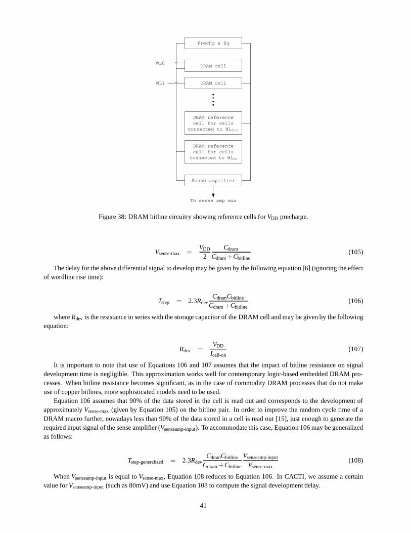
To sense amp mux
Prechg & Eq
DRAM cell
DRAM cell
DRAM reference
cell for cells
connected to WL2n-1
DRAM reference
cell for cells
connected to WL2n
Sense amplifier
WL0
WL1
Figure 38: DRAM bitline circuitry showing reference cells for VDD precharge.
Vsense-max =VDD
2Cdram
Cdram+Cbitline(105)
The delay for the above differential signal to develop may begiven by the following equation [6] (ignoring the effectof wordline rise time):
Tstep = 2.3RdevCdramCbitline
Cdram+Cbitline(106)
whereRdev is the resistance in series with the storage capacitor of theDRAM cell and may be given by the followingequation:
Rdev =VDD
Icell-on(107)
It is important to note that use of Equations 106 and 107 assumes that the impact of bitline resistance on signaldevelopment time is negligible. This approximation works well for contemporary logic-based embedded DRAM pro-cesses. When bitline resistance becomes significant, as in the case of commodity DRAM processes that do not makeuse of copper bitlines, more sophisticated models need to beused.
Equation 106 assumes that 90% of the data stored in the cell isread out and corresponds to the development ofapproximatelyVsense-max(given by Equation 105) on the bitline pair. In order to improve the random cycle time of aDRAM macro further, nowadays less than 90% of the data storedin a cell is read out [15], just enough to generate therequired input signal of the sense amplifier (Vsenseamp-input). To accommodate this case, Equation 106 may be generalizedas follows:
Tstep-generalized = 2.3RdevCdramCbitline
Cdram+Cbitline
Vsenseamp-input
Vsense-max(108)
WhenVsenseamp-inputis equal toVsense-max, Equation 108 reduces to Equation 106. In CACTI, we assume a certainvalue forVsenseamp-input(such as 80mV) and use Equation 108 to compute the signal development delay.
41

When rise time of the wordline is also considered, the bitline delay (Tbitline) of DRAM may be calculated using thesame methodology that was used for SRAM (Equation 53 in Section 6).
The time taken to write data back into a DRAM cell after a read depends on the time taken for the charge transfer totake place between the bitline and the DRAM and may be given bythe following equation:
Twriteback = Tstep (109)
9.3.2 Multisubbank Interleave Cycle Time
For a DRAM array, we consider three timing characteristics:random access time, random cycle time and multibankinterleave cycle time. Calculation of random access time makes use of the same equations that were used for calculationof random access time of an SRAM array (in Section 6). For a DRAM array, typically there are two kinds of cycle time:random cycle time and multibank interleave cycle time. Random cycle time has the same meaning as the random cycletime of an SRAM viz. it is the time interval between two successive random accesses. This time interval is typicallylimited by the time it takes to activate a wordline, sense thedata, write back the data, and then precharge the bitlines.Random cycle time can thus be calculated using the followingequation:
Trandom-cycle = Trow-dec-driver+Tbitline +Tsenseamp+Twriteback+Twordline-reset+ (110)
max(Tbitline-precharge,Tbit-mux-out-precharge,Tsenseamp-mux-out-precharge)
In order to improve the rate at which a DRAM array is accessed so that it is not limited by the random cycle time ofthe array, DRAM arrays usually employ the concept of multibank interleaving. Multibank interleaving takes advantageof the fact that while random access to a particular bank is limited by the random cycle time, accesses to other banksneed not be. With multibank interleaving, accesses to multiple DRAM banks that are on the same address/data bus areinterleaved at a rate defined by themultibank interleave cycle time. In our terminology, eachbankin an array has its ownaddress and data bus and may be concurrently accessed. For our array organization, the concept of multibank interleavedmode is relevant to subbank access and not bank access, so in the rest of this discussion we use the terminology ofmultisubbank interleave mode and multisubbank interleavecycle. Thus, the multisubbank interleave cycle time is therate at which accesses may be interleaved between differentsubbanks of a bank. The multisubbank interleave cycletime depends on the degree of pipelining employed in the request and reply networks of a subbank, and is limited bythe pipelining overhead. We assume minimum pipeline overhead and use the following simple equation to calculatemultisubbank-interleave cycle time:
Tmultisubbank-interleave = max(Trequest-network+Trow-predec,Treply-network) (111)
9.3.3 Retention Time and Refresh Period
An equation for the retention time of a DRAM array may be written as follows [16]:
Tretention =Cdram-cell∆Vcell-worst
Iworst-leak(112)
where∆Vcell-worst is the worst-case change in the voltage stored in a DRAM cell which leads to a read failure, andIcell-worst-leakis the worst-case leakage in a DRAM cell.
We assume that∆Vcell-worst is limited byVmin-sense, the minimum input signal that may be detected by the bitlinesense amplifier. Thus, for a given array organization,∆Vcell-worst may be calculated by solving the following equationfor ∆Vcell-worst:
Vmin-sense =Cdram-cell
Cdram-cell+Cbitline(VDD
2−∆Vcell-worst) (113)
42

If we assume that the differential voltage detected by the sense amplifier is independent of array organization, thenthis means that different array partitions would have different retention times depending on the charge transfer ratiobetween the DRAM cell and the bitlines. For each array organization, it’s thus possible to calculate the value for∆Vcell-worst using Equation 113, which may then be plugged into Equation 112 to find the retention time for that arrayorganization.
The upper bound on the refresh period of a DRAM cell would be equal to its retention time. We assume that a safetymargin of 10% with respect to the retention time is built intothe refresh period and thus calculate the refresh periodusing the following equation:
Trefresh = 0.9Tretention (114)
9.4 DRAM Power Model
During the read of a 0 from a DRAM cell, the true bitline is pulled down to GND during the writeback. Energy isthen consumed in restoring the bitline toVDD during the precharge operation. During the read of a 1 from a DRAMcell, because of our assumption ofVDD-precharge, the voltage of the true bitline does not change but the voltage of thecomplementary bitline gets pulled down to GND and needs to berestored toVDD. So for DRAM, the power consumedin a bitline during a read may be approximated by the following equation:
Edyn-read-bitline = CbitlineVDD2 (115)
9.4.1 Refresh Power
Refreshing the data in each cell of the array consumes power.In order to carry out refresh, every cell in the array needsto be accessed, its data read out, and then written back.
Prefresh =Erefresh
Trefresh(116)
Erefresh = Erefresh-predec-blks+Erefresh-row-dec-drivers+Erefresh-bitlines (117)
Erefresh-predec-blks = NbanksNsubbanksNmats-in-subbankEdyn-mat-predec-blks (118)
Erefresh-row-dec-drivers = 4NbanksNsubbanksNmats-in-subbankEdyn-mat-row-dec-drivers (119)
Erefresh-bitlines = 4NbanksNsubbanksNmats-in-subbankNsubarr-colsEdyn-read-bitline (120)
9.5 DRAM Area Model
9.5.1 Area of Reference Cells
As mentioned earlier in Section 9.2.2, the use ofVDD-precharge leads to the use of reference cells in the array [5]. Forour array organization, this means that there are two additional wordlines per subarray.
9.5.2 Area of Refresh Circuitry
In order to enable continued scaling of a logic-based embedded DRAM cell in terms of performance and cell area, [45]describes a new scalable embedded DRAM cell that makes use ofan access transistor with an intermediate gate-oxide ofmoderate thickness (2.2nm for 90/65nm). This transistor isa standard offering in the logic process which incorporatesthe embedded DRAM. Conventional cells [14] in earlier technologies made use of access transistors with much thickergate-oxides. An effect of the scalable embedded DRAM cell described in [45] is that it results in the cell having alower retention time and a lower refresh period (because of higher worst-case leakage - 10s of pAs compared to 1 fAfor commodity DRAM). The macro discussed in [18] that makes use of the cell described in [45] has a refresh period of64µscompared to conventional macros which have refresh period of 64 ms. This low refresh period required innovation
43

Parameter Meaning Unit
Cdram Storage capacitance of a DRAM cell FAdram-cell Area occupied by the DRAM cell mm2
ARdram-cell Aspect ratio of the DRAM cellVDDdram-cell Voltage representing a 1 in a DRAM cell VVth-dram-acc-transistor Threshold voltage of DRAM cell access transistor mVLdram-acc-transistor Length of DRAM cell access/wordline transistor nmWdram-acc-transistor Width of DRAM cell access transistor nmEOTdram-acc-transistor Equivalent oxide thickness of DRAM access transistors nmIon-dram-cell DRAM cell on-current under nominal conditions µAIoff-dram-cell DRAM cell off-current under nominal conditions pAIworst-off-dram-cell DRAM cell off-current under worst-case conditions A/µVPP Boosted wordline voltage applied to gate of access transistor VIon-dram-wordline-transistor On-current of wordline transistor µA/µ
Table 7: Characteristics of the DRAM cell and wordline driver.
Parameter 90nm 65nm
Cdram (F) 20 20Adram-cell (F - feature size) 20.7F2 25.6F2
VDDdram-cell 1.2 1.2Vth-dram-acc-transistor 350 350Ldram-acc-transistor(nm) 120 120Wdram-acc-transistor 140 90Ion-dram-cell(µA) 45 36Ioff-dram-cell (pA) 2 2VPP 1.5 1.5
Table 8: DRAM technology data for 90nm and 65nm from [18,45].
at the circuit level through the development of a concurrentrefresh scheme described in [18] in order to guarantee highavailability of the DRAM macro. This concurrent refresh scheme adds an extra bank select port to each bank (subbankin our terminology) thereby allowing for concurrent memoryaccess and bank refresh operations in different banks. Eachbank is equipped with a row address counter that contains theaddress of the row to be refreshed. A concurrent refreshscheduler composed of an up-shift-register and a down-shift-register is required in order to generate the bank selectsignals.
Because we loosely base the parameters of our logic-based embedded DRAM technology on information presentedin [5, 18, 45], we model the overhead of the concurrent refresh scheme on area. For our organization in which eachsubbank has multiple mats, we assume that each mat incurs overhead of a row address counter placed at the center ofthe mat. Because of the requirements of the design of the concurrent refresh scheme, for our organization, we assumeNsubbanks-in-matnumber of concurrent refresh schedulers per bank.
9.6 DRAM Technology Modeling
9.6.1 Cell Characteristics
Similar to the SRAM technology assumptions, we assume two types of transistors in the DRAM array. One transistortype is used in the DRAM cell and wordline driver, while the other is used in the rest of the peripheral and globalcircuitry. Table 3 showed a list of transistor characteristics used in CACTI. Table 7 shows characteristics of the DRAMcell and wordline driver that we consider in our model.
We obtain embedded DRAM technology data for four technologynodes – 90, 65, 45, and 32 nm – by using an
44

Parameter 90nm 65nm 45nm 32nm
Cdram (F) 20 20 20 20Adram-cell (F - Feature size) 20.7F2 25.6F2 30.4F2 30.6F2
VDDdram-cell (V) 1.2 1.2 1.1 1.1Vth-dram-acc-transistor(mV) 455 438 446 445Ldram-acc-transistor(nm) 120 120 78 56Wdram-acc-transistor(nm) 140 90 79 56Ion-dram-cell(µA) 45 36 36 36Ioff-dram-cell (pA) 2 2 2 2Iworst-off-dram-cell(pA) 21.1 19.6 19.5 18.9VPP (V) 1.6 1.6 1.5 1.5
Table 9: Characteristics of DRAM cell for the four technology nodes.
approach that makes use of published data, transistor characterization using MASTAR, and our own scaling projections.For 90 nm and 65 nm, we use technology data from [18,45]; Table8 shows this data. In order to obtain technology datafor the 45nm and 32nm technology nodes, we make the followingscaling assumptions:
1. Capacitance of the DRAM cell is assumed to remain fixed at 20fF;
2. The nominal off-current is assumed to remain fixed at 2pA for the cell;
3. Gate oxide thickness is scaled slowly in order to keep gateleakage low and subthreshold current as the dominantleakage current. It has a value of 2.1 nm for 45 nm and 2 nm for 32nm;
4. VDDdram-cell is scaled such that the electric field in the dielectric of theDRAM (VPP/EOTdram-acc-transistor) accesstransistor remains almost constant;
5. There is excellent correlation in the 180–130nm (for conventional thick-oxide device) and 90–65nm (for theintermediate-oxide device) scaling-factors for width andlength of the DRAM cell access transistor. We assumethat there would be good correlation in the 130–90nm and 65–45nm scaling-factors as well. For 32 nm, we assumethat the width and length are scaled in the same proportion asfeature size;
6. We calculate area of the DRAM cell using the equationAdram-cell = 10Wdram-acc-transistorLdram-acc-transistor. Thisequation has good correlation with the actual cell area of the 90 and 65 nm cells that made use of the intermediate-oxide based devices; and
7. We simply assume that nominal on-current of the cell can bemaintained at the 65 nm value. This would requireaggressive scaling of the series parasitic resistance of the transistor.
With these scaling assumptions, we use MASTAR to model the transistors. It is assumed that the resulting channeldoping concentrations calculated by MASTAR would be feasible. Table 9 summarizes the characteristics of the DRAMcell for the four technology nodes.
10 Cache Modeling
In this section we describe how a cache has been modeled in version 5. The modeling methodology is almost identicalto earlier versions of CACTI with a few changes that simplifythe code.
10.1 Organization
As described in [47], a cache has a tag array in addition to a data array. In earlier versions of CACTI the data and tagarrays were modeled separately with separate code functions even though the data and tag arrays are structurally very
45

Input tag bitsH1
H2
V0
H2
V0V0 V0
Way select signals to
data array
Stored tag bits
Tag input bits over
request H-tree
Tag match
outputs
Comparators
at mat
Sense amps
at mat
Comparators
at mat
Sense amps
at mat
Comparators
at mat
Sense amps
at mat
Comparators
at mat
Sense amps
at mat
Tag match outputs over
reply H-tree
Figure 39: Organization of a set-associative tag array.
similar. The essential difference between the tag array andthe data array is that the tag array includes comparators thatcompare the input tag bits with the stored tags and produce the tag match output bits. Apart from the comparators, therest of the peripheral/global circuitry and memory cells are identical for data and tag arrays. In version 5, we leveragethis similarity between the data and tag arrays and use the same set of functions for their modeling. For the tag array,we reuse the comparator area, delay, and power models.
Figure 39 illustrates the organization of a set-associative tag array. Each mat includes comparators at the outputs ofthe sense amplifiers. These comparators compare the stored tag bits with the input tag bits and produce the tag matchoutput bits. These tag match output signals are the way-select signals that serve as inputs to the data array. The way-select signals traverse over the vertical and horizontal H-trees of the tag array to get to the edge of the tag array fromwhere they are shipped to the data array. For a cache of normalaccess type, these way-select signals then enter the dataarray where, like the address and datain signals, they travel along the horizontal and vertical H-tree networks to get tomats in the accessed subbank. At the mats, these way-select signals are ‘anded’ with sense amplifier mux decode signals(if any) and the resultant signals serve as select signals for the sense amplifier mux which generates the output wordfrom the mat.
10.2 Delay Model
We present equations for access and cycle times of a cache. The access time of a cache depends on the type of cacheaccess (normal, sequential, or fast [40]).
The equation for access time of a normal cache which is set-associative is as follows:
Taccess-normal-set-associative= max(Ttag-arr-access+Tdata-arr-request-network+Tdata-arr-senseamp-mux-decode,
Tdata-arr-request-network+Tdata-arr-mat)+Tdata-arr-reply-network (121)
Ttag-arr-access = Ttag-arr-request-network+Ttag-arr-mat+Ttag-arr-reply-network (122)
In the above equation,Ttag-arr-access, the access time of the tag array, is calculated using the following equation.
46

Ttag-arr-access = Ttag-arr-request-network+Ttag-arr-mat+Ttag-arr-reply-network+Tcomparators (123)
The equation for access time of a normal cache which is direct-mapped is as follows:
Taccess-normal-direct-mapped= max(Ttag-arr-access,Tdata-arr-access) (124)
The equation for access time of a sequentially accessed (tagarray is accessed first before data array access begins)cache is as follows:
Taccess-sequential = Ttag-arr-access+Tdata-arr-access (125)
The equation for access time of a ‘fast’ cache (late way-select multiplexing) cache is as follows:
Taccess-fast = max(Ttag-arr-access,Tdata-arr-access)+Tway-select-mux (126)
whereTway-select-muxis the delay through the way-select mux. The way-select mux is assumed to be placed at theedge of the data array and selects the appropriate output word corresponding to the correct way (which is selected basedon the way-select signals from the tag array).
10.3 Area Model
Total area of the cache is calculated by simply adding the areas occupied by the tag and data arrays.
Acache = Adata-array+Atag-array (127)
Atag-arrayis calculated using the equations presented in Section 5 with the area of the comparators also added.
10.4 Power Model
The dynamic energy consumed in the cache and its standby leakage power are calculated by simply adding their valuesfor the data and tag arrays. For the tag array, the leakage in the comparators is also considered.
Edyn-energy-cache = Edyn-energy-data-array+Edyn-energy-tag-array (128)
Pleak-cache = Pleak-data-array+Pleak-tag-array (129)
11 Quantitative Evaluation
In this section we evaluate the impact of new CACTI 5 features. We also compare results from CACTI 5.1 with version4.2 in order to give users an idea of what to expect when upgrading to CACTI 5.1.
11.1 Evaluation of New CACTI 5 Features
Table 10 shows the default parameters that we have used whilecarrying out the evaluation of new CACTI 5 features.For this evaluation we use plain RAMs instead of caches. In Section 12, we show results for caches. For each study, wepresent charts that show the following metrics: access time, random cycle time, area, dynamic energy per read access,and standby leakage power.
47

Parameter Value
Capacity (MB) 16Output width (bits) 512Number of banks 1Number of read/write ports 1Number of exclusive read ports 0Number of exclusive write ports 0Technology-node (nm) 65DRAM Nomax area constraint 40max acc time constraint 10max repeater delay constraint 10Optimize for dynamic energy NoOptimize for dynamic power NoOptimize for leakage power NoOptimize for cycle time YesTemperature (K) 360SRAM cell/wordline technology flavor ITRS HPPeripheral/Global circuitry technology flavorITRS HPInterconnect projection type ConservativeWire type inside mat Semi-globalWire type outside mat Semi-global
Table 10: CACTI input parameters
11.1.1 Impact of New CACTI Solution Optimization
Figure 40 shows the impact of varyingmax area constraint (that was described in Section 2.5.1) for a 16MB SRAM.As max area constraint is increased, the number of subarrays in the SRAM is allowed to grow, and so the area growssteadily. As the number of subarrays increases, the components of delay within a mat decreases and the access timefalls up to a point after which it starts to increase again. The random cycle time keeps decreasing as the number ofsubarrays increases because the wordline and bitline delays keep getting smaller. The trend for dynamic read energy peraccess shows some up-and-down variation. For our assumed CACTI cache organization, an increase in Ndwl typicallyincreases the dynamic energy consumption because more wordlines are activated per read access, while an increase inNdbl typically decreases the dynamic energy consumption because of reduction in bitline power. The standby leakagepower keeps growing as the area of the RAM increases.
Figure 41 shows the impact of varyingmax acc time constraint. For the assumed set of SRAM parameters, itcan be seen that the solution with best access time (corresponding tomax acc time constraint of 0) also has the bestdynamic read energy per access. So further relaxation of themax acc time constraint does not lead to any energyreduction benefits in this case.
Figure 42 shows the impact of varyingmax repeater delay constraint. Themax repeater delay constraint
changes the separation distance and sizing of repeaters/buffers in the H-tree networks and is useful for trading off delayfor energy benefits. It can be seen here that varyingmax repeater delay constraint does not lead to energy savingsmuch unless the access time is allowed to degrade heavily. Initially, asmax repeater delay constraint is increasedfrom 0 to 20%, it can be seen that the access time does not change and there are no energy savings. This is because ofthe maximum limit that we have imposed on transistor size in CACTI. For values ofmax repeater delay constraint
between 0 and 20%, the sizing of the repeater comes out to be larger than the maximum allowed transistor size and istherefore being fixed at the maximum allowed transistor size(the maximum allowed transistor size was fixed at 100F(F = feature size) for NMOS transistors). For amax repeater delay constraint of 400% there is significant energysavings but with a disproportionate degradation of access time.
48

0
5
10
15
20
25
30
0 5 10 15 20 25 30 35 40 45 50
max_area_constraint (%)
Acc
ess
tim
e (n
s)
0
5
10
15
20
25
0 5 10 15 20 25 30 35 40 45 50
max_area_constraint (%)
Ran
do
m c
ycle
tim
e (n
s)
0
50
100
150
200
250
0 5 10 15 20 25 30 35 40 45 50
max_area_constraint (%)
Are
a (m
m2)
0
2
4
6
8
10
12
0 5 10 15 20 25 30 35 40 45 50
max_area_constraint (%)
Dyn
amic
rea
d e
ner
gy
per
acc
ess
(nJ)
0
5000
10000
15000
20000
25000
30000
35000
0 5 10 15 20 25 30 35 40 45 50
max_area_constraint (%)
Sta
nd
by
leak
age
po
wer
per
ban
k (m
W)
0
20
40
60
80
100
120
140
0 5 10 15 20 25 30 35 40 45 50
max_area_constraint (%)
Nd
wl,
Nd
bl a
nd
Nsp
d
Ndwl
Ndbl
Nspd
Figure 40: Access time, random cycle time, area, dynamic energy, and leakage power of a 16MB SRAM asmax area constraint is varied.
Figure 43 shows the impact of optimizing the solution generated by CACTI for a 16MB SRAM in different ways.Table 11 shows the different optimization scenarios targeting metrics of random cycle time, dynamic read energy peraccess, dynamic power, and standby leakage power. The percentage variation between the worst and best values foreach metric shown in Figure 43 is as follows: access time (4%), random cycle time (273%), area (28%), dynamic readenergy per access (38%), and standby leakage power (24%). These variations illustrate the dependence of RAM andcache performance estimation on the kind of optimization that is applied.
11.1.2 Impact of Device Technology
Figure 44 illustrates the tradeoffs associated with assuming different types of devices in the memory cells/wordlinedrivers and the rest of the peripheral/global circuitry. Three scenarios are considered:
1. ITRS HP only;
49

0
1
2
3
4
5
6
7
8
9
0 5 10 15 20 25 30 35 40 45 50
max_acc_time_constraint (%)
Acc
ess
tim
e (n
s)
0
0.2
0.4
0.6
0.8
1
1.2
0 5 10 15 20 25 30 35 40 45 50
max_acc_time_constraint (%)
Ran
do
m c
ycle
tim
e (n
s)
0
20
40
60
80
100
120
140
160
180
200
0 5 10 15 20 25 30 35 40 45 50
max_acc_time_constraint (%)
Are
a (m
m2)
0
1
2
3
4
5
6
0 5 10 15 20 25 30 35 40 45 50
max_acc_time_constraint (%)
Dyn
amic
rea
d e
ner
gy
per
acc
ess
(nJ)
0
5000
10000
15000
20000
25000
30000
0 5 10 15 20 25 30 35 40 45 50
max_acc_time_constraint (%)
Sta
nd
by
leak
age
po
wer
per
ban
k (m
W)
Figure 41: Access time, random cycle time, area, dynamic energy, and leakage power of a 16MB SRAM asmax acc time constraint is varied.
Optimization Optimize for Optimize for Optimize for Optimize forScenario random cycle time dynamic energy dynamic power leakage powerA Yes No No NoB Yes Yes No NoC No Yes No NoD No No Yes NoE No No No YesF Yes Yes Yes Yes
Table 11: Different solution optimization scenarios targeting metrics of random cycle time, dynamic read energy peraccess, dynamic power, and standby leakage power.
50

0
5
10
15
20
25
0 10 20 30 40 50 60 70 80 90 100 200 400 800
max_repeater_delay_constraint (%)
Acc
ess
tim
e (n
s)
0
0.5
1
1.5
2
2.5
3
3.5
0 10 20 30 40 50 60 70 80 90 100 200 400 800
max_repeater_delay_constraint (%)
Ran
do
m c
ycle
tim
e (n
s)
0
20
40
60
80
100
120
140
160
180
0 10 20 30 40 50 60 70 80 90 100 200 400 800
max_repeater_delay_constraint (%)
Are
a (m
m2)
0
0.5
1
1.5
2
2.5
3
3.5
4
4.5
5
0 10 20 30 40 50 60 70 80 90 100 200 400 800
max_repeater_delay_constraint (%)
Dyn
amic
rea
d e
ner
gy
per
acc
ess
(nJ)
0
5000
10000
15000
20000
25000
30000
0 10 20 30 40 50 60 70 80 90 100 200 400 800
max_repeater_delay_constraint (%)
Sta
nd
by
leak
age
po
wer
per
ban
k (m
W)
Figure 42: Access time, random cycle time, area, dynamic energy, and leakage power of a 16MB SRAM asmax repeater delay constraint is varied.
2. ITRS LSTP (memory cells/wordline drivers) + ITRS HP (peripheral/global circuitry);
3. ITRS LSTP only;
It can be seen that the areas of RAMs for the 3 considered scenarios remain more or less the same. With respect to“ITRS HP only”, on average over the considered capacities, “ITRS LSTP + ITRS HP” exhibits an improvement of 76%in the standby leakage power. This improvement comes at the cost of 11% worse access time and 39% worse randomcycle time. “ITRS LSTP only” shows an improvement of almost 100% in standby leakage power with respect to “ITRSHP only”, and this improvement comes at a cost of 159% worse access time and 246% worse random cycle time.
51

0
1
2
3
4
5
6
7
8
A B C D E F
Optimization scenarios
Acc
ess
tim
e (n
s)
0
0.5
1
1.5
2
2.5
A B C D E F
Optimization scenarios
Ran
do
m c
ycle
tim
e (n
s)
0
20
40
60
80
100
120
140
160
180
A B C D E F
Optimization scenarios
Are
a (m
m2)
0
0.5
1
1.5
2
2.5
3
3.5
4
A B C D E F
Optimization scenarios
Dyn
amic
rea
d e
ner
gy
per
acc
ess
(nJ)
0
5000
10000
15000
20000
25000
30000
A B C D E F
Optimization scenarios
Sta
nd
by
leak
age
po
wer
per
ban
k (m
W)
Figure 43: Access time, random cycle time, area, dynamic energy, and leakage power of a 16MB SRAM under differentoptimization function scenarios.
11.1.3 Impact of Interconnect Technology
Figure 45 illustrates the dependence of RAM/cache performance on interconnect technology assumptions. As describedin Section 8 on “Technology Modeling”, instead of assuming asingle set of scaling assumptions for interconnect tech-nology, we consider aggressive and conservative scaling projections as in [11, 13]. From Figure 45, it can be seen thatfor the SRAM capacities and technology (65nm) considered, the cache performance is not very different under eitherconservative or aggressive interconnect technology assumptions. The lower resistance per unit length of the aggressiveprojections leads to lowering of the access time by about 11%on an average. For smaller technologies, the impact ofinterconnect technology assumptions would be more.
Figure 46 shows the impact of wire type on cache performance.As described in Section 8 on “Technology Model-ing”, wires outside a mat can be of either ‘semi-global’ or ‘global’ type. With respect to semi-global type, global typewires outside mats lead to an improvement in access time of 22% on an average with about 3% increase in area. The
52
0
5
10
15
20
25
30
1 2 4 8 16 32
Capacity (MB)
Acc
ess
tim
e (n
s)
ITRS HP in mem cell and periph-global
ITRS LSTP in mem cell, ITRS HP in periph-global
ITRS LSTP in mem cell and periph-global
0
0.5
1
1.5
2
2.5
3
1 2 4 8 16 32
Capacity (MB)
Ran
do
m c
ycle
tim
e (n
s)
ITRS HP in mem cell and periph-global
ITRS LSTP in mem cell, ITRS HP in periph-global
ITRS LSTP in mem cell and periph-global
0
50
100
150
200
250
300
350
400
1 2 4 8 16 32
Capacity (MB)
Are
a (m
m2)
ITRS HP in mem cell and periph-global
ITRS LSTP in mem cell, ITRS HP in periph-global
ITRS LSTP in mem cell and periph-global
0
1
2
3
4
5
6
7
1 2 4 8 16 32
Capacity (MB)
Dyn
amic
rea
d e
ner
gy
per
acc
ess
(nJ)
ITRS HP in mem cell and periph-global
ITRS LSTP in mem cell, ITRS HP in periph-global
ITRS LSTP in mem cell and periph-global
1 2 4 8 16 32
0 5000
10000
15000
20000
25000
30000
35000
40000
45000
50000
Sta
nd
by
leak
age
po
wer
per
ban
k
(mW
)
Capacity (MB)
ITRS HP in mem cell and periph-global
ITRS LSTP in mem cell, ITRS HP in periph-global
ITRS LSTP in mem cell and periph-global
Figure 44: Access time, random cycle time, area, dynamic energy, and leakage power of SRAMs for different 65nmdevice technology assumptions.
global type wires take up greater area than the semi-global type wires, so the number of mats in the bank with globalwire type is fewer than that with semi-global wire type. Thisleads to increase in the random cycle time because ofgreater wordline and bitline delays.
11.1.4 Impact of RAM Cell Technology
Figure 47 illustrates the dependence of cache performance on the type of RAM cell technology – SRAM or logic-basedembedded DRAM. For each capacity, the properties of SRAMs and DRAMs shown in Figure 47 are for CACTI solutionswith the best access time amongst all solutions. It can be seen from this figure that up to about 2 MB capacity, the accesstime of SRAM is lower after which the access time of DRAM becomes lower. This is because of the decreased wiredelay experienced in DRAMs which occupy a much smaller area compared to the SRAMs. For the larger-capacityRAMs (≥ 1MB), on average over all capacities, the area of the DRAMs isabout a factor of 2.6 smaller than that of
53

0
2
4
6
8
10
12
1 2 4 8 16 32
Capacity (MB)
Acc
ess
tim
e (n
s)
Conservative interconnect projections
Aggressive interconnect projections
0
0.1
0.2
0.3
0.4
0.5
0.6
0.7
0.8
0.9
1
1 2 4 8 16 32
Capacity (MB)
Ran
do
m c
ycle
tim
e (n
s)
Conservative interconnect projections
Aggressive interconnect projections
0
50
100
150
200
250
300
350
400
1 2 4 8 16 32
Capacity (MB)
Are
a (m
m2)
Conservative interconnect projections
Aggressive interconnect projections
0
1
2
3
4
5
6
1 2 4 8 16 32
Capacity (MB)
Dyn
amic
rea
d e
ner
gy
per
acc
ess
(nJ)
Conservative interconnect projections
Aggressive interconnect projections
0
10000
20000
30000
40000
50000
60000
1 2 4 8 16 32
Capacity (MB)
Sta
nd
by
leak
age
po
wer
(m
W)
Conservative interconnect projections
Aggressive interconnect projections
Figure 45: Access time, random cycle time, area, dynamic energy, and leakage power of SRAMs under aggressive andconservative interconnect technology assumptions.
the SRAMs. Because of the destructive read out from a capacitor and the subsequent writeback, it can be seen that therandom cycle time of the DRAM is much higher than that of the SRAM. On an average over all capacities it is higherby a factor of about 2.2. However, it can be seen that the multisubbank interleave cycle time of the DRAMs can comeclose to the random cycle time of SRAMs up to about 4 MB. With further pipelining in the request and reply networks,the multisubbank interleave cycle time can be improved further.
The standby leakage power of the DRAM is much lower than that of the SRAMs because of the use of the low-leakage 1T cell. For the larger-capacity RAMs (≥ 1MB), on average the standby leakage power of DRAMs is lowerthan that of SRAMs by a factor of about 6. For the larger-capacity RAMs, on average the dynamic read energy peraccess of the DRAMs is more or less the same as that of the SRAMs. It is important to note that the comparisonspresented here were for SRAMs and DRAMs with the best access time amongst all solutions.
54

0
2
4
6
8
10
12
1 2 4 8 16 32
Capacity (MB)
Acc
ess
tim
e (n
s)
Semi-global type wires outside mat
Global type wires outside mat
0
0.1
0.2
0.3
0.4
0.5
0.6
0.7
0.8
0.9
1
1 2 4 8 16 32
Capacity (MB)
Ran
do
m c
ycle
tim
e (n
s)
Semi-global type wires outside mat
Global type wires outside mat
0
50
100
150
200
250
300
350
400
1 2 4 8 16 32
Capacity (MB)
Are
a (m
m2)
Semi-global type wires outside mat
Global type wires outside mat
0
1
2
3
4
5
6
1 2 4 8 16 32
Capacity (MB)
Dyn
amic
rea
d e
ner
gy
per
acc
ess
(nJ)
Semi-global type wires outside mat
Global type wires outside mat
0
10000
20000
30000
40000
50000
60000
1 2 4 8 16 32
Capacity (MB)
Sta
nd
by
leak
age
po
wer
(m
W)
Semi-global type wires outside mat
Global type wires outside mat
Figure 46: Access time, random cycle time, area, dynamic energy, and leakage power of SRAMs with “global” inter-connect type used for wires outside the mat.
11.2 Version 4.2 vs Version 5.1 Comparisons
We first present the differences in the technology metrics ofversions 4.2 and 5.1. Figure 48 shows FO4 delays forversions 4.2 and 5.1. For version 5, the FO4 delay has been shown for the ITRS HP device type. It can be seen that,surprisingly, there is good agreement between the FO4 delays of versions 4.2 and 5.1, particularly at the 65nm and 45nmnodes.
Figures 49, 50 and 51 shows the trends for resistance per unitmicron, capacitance per unit micron and unbuffereddelay for a wire of length 1-micron for versions 4.2 and 5.1. For version 4.2, trends are shown for both ‘local’ and‘global’ wire types which were discussed in Section 2.3. Forversion 5.1, trends are shown for both ‘semi-global’ and‘global’ wire types and for both aggressive and conservative assumptions of interconnect technology as discussed inSection 8.2. It can be seen that the unbuffered wire delay of the local wire type of version 4.2 is greater than that of thesemi-global wire type of version 5.1 by a factor of about 3.5.
55

Figure 52 compares results generated by CACTI version 4.2 and version 5.1. For version 5.1, we show three solutions– solutions with best access time, best area and best dynamicread energy per access. We also show results from amodified version of version 4.2. In the modified version, we increase the limits defined for Ndwl, Ndbl, Nspd, numberof subarrays, and number of segments allowed in the H-trees.Increasing these set limits allows a richer exploration ofthe search space of array partitions, particularly for large SRAMs. We call this version, version 4.2-limits-removed.
Because of significant modeling differences between versions 4.2 and 5.1, it is not easy to compare and analyze thebehavior of the two versions, but we make general observations and present high-level plausible reasons for the trends.Firstly, regarding area, we observe that the areas of solutions produced by version 5.1 are much greater than that ofthe version 4.2 solution. Version 5.1 has made a major updateto the area model and has introduced new features suchas inclusion of ECC and redundancy overheads which increasearea overhead. Also version 5.1 makes use of a biggerSRAM cell at 146F2 compared to the 120F2 cell used in version 4.2. For the 32 MB SRAM, the solution generated byversion 4.2-limits-removed has an area of 343 mm2 which is greater than the areas of all version 5.1 solutions.
Regarding access time, it can be seen that the access times for the best access time and best dynamic energy solutionsof version 5.1 are much lower and scale in a much better way compared to the version 4.2 solution. The access timeof the 32 MB SRAM gets better with version 4.2-limits-removed, however, it’s still much worse than the access timeof the version 5.1 best access time and best dynamic energy solutions. The main reason for the larger access times ofversion 4.2 is because of the high resistance per unit lengthof the local wires in version 4.2.
Regarding dynamic energy, it can be seen that the dynamic energy per read access of the version 5.1 best accesstime and best dynamic energy solutions are greater than thatof version 4.2 by a factor of about 5 on an average. Thisis mainly because of the organization that has been assumed in version 5.1 in which wordlines and bitlines in multiplemats are activated per access. Also, as described in Section2.2, bugs in version 4.2 with respect to dynamic energy ofrouting in the H-trees causes the dynamic energy per read access to be underestimated.
Leakage power is heavily dependent on the underlying technology data. The standby leakage of version 4.2 is greaterthan that of the best access time and best dynamic energy solutions of version 5.1 by a factor of about 3 on an average.
56

0
2
4
6
8
10
12
8K
16K
32K
64K
128K
256K
512K
1M
2M
4M
8M
16
M
32M
Capacity (bytes)
Acc
ess
tim
e (n
s)
SRAM
DRAM
0
0.5
1
1.5
2
2.5
3
8K
16K
32K
64K
128K
256K
512K
1M
2M
4M
8M
16M
32M
Capacity (bytes)
Cyc
le t
ime
(ns)
SRAM random
DRAM random
DRAM multisubbank interleave
0
0.5
1
1.5
2
2.5
3
3.5
4
8K 16K 32K 64K 128K 256K 512K
Capacity (bytes)
Are
a (m
m2)
SRAM
DRAM
0
50
100
150
200
250
300
1M 2M 4M 8M 16M 32M
Capacity (bytes)
Are
a (m
m2)
SRAM
DRAM
0
0.05
0.1
0.15
0.2
0.25
0.3
0.35
0.4
0.45
0.5
8K 16K 32K 64K 128K 256K 512K
Capacity (bytes)
Dyn
rea
d e
ner
gy
per
rea
d a
cces
s
(nJ)
SRAM
DRAM
0
1
2
3
4
5
6
1M 2M 4M 8M 16M 32M
Capacity (bytes)
Dyn
rea
d e
ner
gy
per
rea
d a
cces
s
(nJ)
SRAM
DRAM
0
100
200
300
400
500
600
700
800
8K 16K 32K 64K 128K 256K 512K
Capacity (bytes)
Sta
nd
by
leak
age
po
wer
(m
W) SRAM
DRAM
0
5000
10000
15000
20000
25000
30000
35000
40000
45000
50000
1M 2M 4M 8M 16M 32M
Capacity (bytes)
Sta
nd
by
leak
age
po
wer
(m
W) SRAM
DRAM
Figure 47: Access time, cycle time, area, dynamic read energy per access, and standby leakage power of SRAM andlogic-based embedded DRAM for 65nm technology. The area, dynamic read energy per access, and standby leakagepower trends are split up into two charts based on capacities.
57

0
5
10
15
20
25
90 65 45 32
Technology node (nm)
FO
4 d
elay
(p
s)
v4.2
v5.1
Figure 48: FO4 delays for various technology nodes in versions 4.2 and 5.1. The version 5.1 FO4 delays are for ITRShigh-performance device type.
0
2
4
6
8
10
12
14
16
18
90 65 45 32
Technology node (nm)
Res
ista
nce
per
un
it m
icro
n
(oh
m/m
icro
n)
v4.2 local
v4.2 global
v5.1 semi-global cons
v5.1 semi-global aggr
v5.1 global cons
v5.1 global aggr
Figure 49: Resistance per unit micron of wire at various technology nodes for versions 4.2 and 5.1.
58

0
0.05
0.1
0.15
0.2
0.25
0.3
0.35
0.4
90 65 45 32
Technology node (nm)
Cap
acit
ance
per
un
it m
icro
n
(fF
/mic
ron
)
v4.2 local
v4.2 global
v5.1 semi-global cons
v5.1 semi-global aggr
v5.1 global cons
v5.1 global aggr
Figure 50: Capacitance per unit micron of wire at various technology nodes for versions 4.2 and 5.1.
0
0.0002
0.0004
0.0006
0.0008
0.001
0.0012
0.0014
0.0016
90 65 45 32
Technology node (nm)
Un
bu
ffer
ed w
ire
del
ay f
or
1-m
icro
n
len
gth
wir
e (p
s)
v4.2 local
v4.2 global
v5.1 semi-global cons
v5.1 semi-global aggr
v5.1 global cons
v5.1 global aggr
Figure 51: Unbuffered delays through a wire of length 1-micron for various technology nodes in versions 4.2 and 5.1.The wire delays for version 5.1 are for both aggressive and conservative projections.
59

0
10
20
30
40
50
60
1 2 4 8 16 32
Capacity (MB)
Acc
ess
tim
e (n
s)
v4.2
v4.2-limits-removed
v5.1-best-acc-time
v5.1-best-area
v5.1-best-dyn-energy
0
10
20
30
40
50
60
1 2 4 8 16 32
Capacity (MB)
Ran
do
m c
ycle
tim
e (n
s)
v4.2
v4.2-limits-removed
v5.1-best-acc-time
v5.1-best-area
v5.1-best-dyn-energy
0
50
100
150
200
250
300
350
400
1 2 4 8 16 32
Capacity (MB)
Are
a (m
m2)
v4.2
v4.2-limits removed
v5.1-best-acc-time
v5.1-best-area
v5.1-best-dyn-energy
0
5
10
15
20
25
1 2 4 8 16 32
Capacity (MB)
Dyn
amic
rea
d e
ner
gy
per
acc
ess
(nJ)
v4.2
v4.2-limits removed
v5.1-best-acc-time
v5.1-best-area
v5.1-best-dyn-energy
0
20000
40000
60000
80000
100000
120000
1 2 4 8 16 32
Capacity (MB)
Sta
nd
by
leak
age
po
wer
(m
W)
v4.2
v4.2-limits removed
v5.1-best-acc-time
v5.1-best-area
v5.1-best-dyn-energy
Figure 52: Access time, random cycle time, area, dynamic energy, and leakage power obtained from versions 4.2 and5.1 for SRAMs in 70nm technology.
60

Parameter Value
Area (mm2) 128Access time (ns) 5Clock frequency (MHz) 800Total power (W) 8
Table 12: Characteristics of Sun’s SPARC 90nm L2 cache.
12 Validation
In this section, we compare the published values of area, delay, and power of real cache designs with the projections ofarea, delay, and power produced by CACTI. The area, delay, and power of a real cache or RAM design are influencedby various factors. The design process inherently makes certain area, delay, and power tradeoffs based on budgets andrequirements. Area, delay, and power are also influenced by design methodology, human bias and other practical consid-erations such as availability of IP from past designs etc. CACTI is based on generic assumptions of cache organization,circuits, design methodology, layout, design rules, and technology, whereas a real cache design is based on specificchoices of all these. With CACTI 5, however, as was shown in the previous section, we provide a number of knobs thatcan be turned in order to try to emulate a real cache design in abetter way. So it is interesting to see how the projectionsproduced by CACTI would compare with real designs.
We use information from real cache specifications to fix as many of the input parameters required by CACTI aspossible, such as capacity, associativity, line size, technology-node, etc. In order to understand and explore area/de-lay/power tradeoffs, we vary parameters such as “maximum percentage away from best area solution” and “maximumpercentage away from best access time solution” within reasonable bounds.
12.1 Sun SPARC 90nm L2 cache
[25] describes the implementation of a 90nm SPARC 4MB L2 cache. Table 12 shows the area, access time, randomcycle time, and power of the SPARC L2 cache. The clock frequency of the CPU core itself is 1.6 GHz but the L2 cachehas a throughput of two clock cycles, so we fix the random cycletime of the L2 cache as 800 MHz.
Table 13 presents the input parameters used with CACTI to model this cache. From the description of the cache, wecould not be sure whether the cache access mode is ‘normal’ or‘fast’, so we try out both scenarios. In order to explorea range of area/delay/power tradeoffs, we varymax area constraint between 0 and 50 andmax delay constraint
between 0 and 30. In order to meet the aggressive random cycletime of the cache, we optimize the solution for randomcycle time only. Because we do not have information about theinterconnect properties of the fabrication process, weconsider both aggressive and conservative projections forinterconnect. Also, for ‘wire type outside mat’, we try outboth ‘semi-global’ and ‘global’ wire types.
Figure 53 shows bubble charts showing access time, area, andpower of the SPARC L2 cache and the various solu-tions generated by CACTI. The charts shown in Figure 53 are for CACTI solutions with ‘fast’ access mode, ‘conserva-tive’ interconnect projections and ‘semi-global’ wire type outside mat. We believe that these values for the parametersare likely to be closest to the actual cache design. Results of the validation exercise with other configuration values arepresented in the appendix. As we do not know the operating conditions corresponding to the published value for powerof the SPARC L2, we compute dynamic power for the CACTI solutions for three activity factors – 0.1, 0.5, and 1.0.Also, we assume that the ratio of read to write accesses is 3. Note that the solutions shown in Figure 53 are the onesthat can meet the random cycle time of the SPARC L2. It can be seen that many solutions have access time, area, andpower that are quite similar to that of the L2 cache. Table 14 shows error percentages of prominent CACTI solutionswith respect to the SPARC L2.
12.2 Intel Xeon 65nm L3 cache
Table 15 shows the area, access time, dynamic power, and leakage power of an Intel Xeon L3 cache in a 65nm process.[9] mentions that the access time of the cache is less than 9 ns; we assume the access time to be 9 ns. The clock
61

Parameter Value
Capacity (MB) 4Line size (bytes) 32Associativity 4Number of read/write ports 1Number of exclusive ports 0Number of banks 1Technology-node (nm) 90Output width (bits) 256Specific tag YesTag width 34Access mode Normal/FastPure RAM No (cache)DRAM NoRepeaters in bank H-trees Yesmax area constraint 0 - 70max acc time constraint 0 - 30max repeater delay constraint 10Optimize for dynamic energy NoOptimize for dynamic power NoOptimize for leakage power NoOptimize for cycle time YesTemperature (K) 360SRAM cell/wordline technology flavor ITRS HPPeripheral/Global circuitry technology flavorITRS HPInterconnect projection type ConservativeWire type inside mat Semi-globalWire type outside mat Semi-global/Global
Table 13: CACTI input parameters used for modeling 90nm SPARC L2 cache
Solution % error in % error in % error in Avg of acc time, areaacc time area power and power % errors
Best % error in acc time 8/8/8 -31/-31/-31 -67/-52/-34 35/30/24Best % error in area 17/17/17 -33/-33/-33 -69/-52/-31 39/34/27Best % error in power 17/8/8 -33/-23/-23 -69/-54/-36 39/28/22Best average of area, acc time, and power % errors8/8/8 -23/-23/-23 -68/-54/-36 33/28/22Best average of area and acc time % errors 8/8/8 -23/-23/-23 -68/-54/-36 33/28/22Best average of acc time and power % errors 8/8/8 -31/-31/-31 -67/-52/-34 35/30/24Best acc time 8/8/8 -31/-31/-31 -67/-52/-34 35/30/24Best area 17/17/17 -33/-33/-33 -69/-52/-31 39/34/27Best power 17/8/8 -33/-23/-23 -69/-54/-36 39/28/22
Table 14: Error percentages of some prominent solutions generated by CACTI with respect to a 90nm SPARC L2 cache.The CACTI solutions assume ‘fast’ access mode, ‘conservative’ interconnect projections, and ‘semi-global’ wire typeoutside mat. We have used 3 activity factors of 0.1, 0.5, and 1, and so each entry in the table has 3 values.
frequency of the core itself is given to be 3.4 GHz and the clock frequency of the L3 is given to be half that of thecore [33]. Also, because the output bus width of the L3 is 256 bits, it would require two cycles to transmit a 64-byte
62

Activity factor for dynamic power = 0.1
0
1
2
3
4
5
6
7
8
0 5 10 15
Power (W)
Acc
ess
tim
e (n
s)
CACTI generated solutions
Target SPARC L2
Activity factor for dynamic power = 0.5
0
1
2
3
4
5
6
7
8
0 5 10 15
Power (W)
Acc
ess
tim
e (n
s)
CACTI generated solutions
Target SPARC L2
Activity factor for dynamic power = 1.0
0
1
2
3
4
5
6
7
8
0 5 10 15
Power (W)
Acc
ess
tim
e (n
s)
CACTI generated solutions
Target SPARC L2
Figure 53: Access time, area, and power of the 90nm SPARC L2 cache and of solutions generated by CACTI. TheCACTI solutions assume ‘fast’ access mode, ‘conservative’interconnect projections, and ‘semi-global’ wire type outsidemat. The 3 plots correspond to 3 activity factors assumed while computing dynamic power for the CACTI-generatedsolutions.
Area (mm2) 200 Measured from die photo [32]Access time (ns) 9 ns [9]Clock frequency (GHz) 850 MHz [33]Dynamic power (W) 1.7/5.4 [7,33,44]Leakage power (W) 6.6 [33,44]
Table 15: Characteristics of Intel Xeon’s 65nm L3 cache.
line, so we fix the random cycle frequency of the L3 to be one-fourth that of the CPU, i.e. 850 MHz. The dynamic powerof the cache comes out to be 5.4W based on information from [33, 44], however [7] mentions that the cache consumesabout 1.7W for “average applications”. We speculate that these differences in dynamic power numbers that have beenquoted are because of different activity factors in the cache caused due to measurements or simulations of applicationswith different characteristics. While carrying out comparisons of the area, delay, and power of the Intel cache with thoseof the solutions generated by CACTI, we use both values of power.
The 65nm process offers transistors with 35nm gate-lengths. The cache itself, however, makes use of longer-channeldevices with lengths that are about 10% longer than the nominal. The longer-channel devices have on-currents that areabout 10% less than the nominal devices but have leakage thatis lower by a factor of 3. The cache operates in a voltagedomain different from that of the cores. The cores can operate at 1.25V while the cache operates at 1.1V.
In order to control leakage in the cache, the Intel cache implements n and p sleep transistors at the level of ‘blocks’within subarrays (Each subarray within the Intel cache is composed of multiple ‘blocks’ with one block within a subarrayactivated per access. The ‘subarray’ of the Intel cache is not the same as that of CACTI). The impact of these sleeptransistors is that leakage power in all blocks that are not activated during an access is cut down by half.
63

Parameter Value
Capacity (MB) 16Line size (bytes) 64Associativity 16Number of read/write ports 1Number of exclusive ports 0Number of banks 2Technology-node (nm) 65Output width (bits) 512Specific tag NoAccess mode SerialPure RAM No (cache)DRAM Nomax area constraint 0 - 50max delay constraint 0 - 30max repeater delay constraint 10Optimize for dynamic energy NoOptimize for dynamic power NoOptimize for leakage power NoOptimize for cycle time YesTemperature (K) 360SRAM cell/wordline technology flavor ITRS HPPeripheral/Global circuitry technology flavorITRS HPInterconnect projection type ConservativeWire type inside mat Semi-globalWire type outside mat Semi-global/Global
Table 16: CACTI input parameters used for modeling 65nm Intel Xeon L3 cache.
Table 16 shows the input parameters used with CACTI to model the Intel L3 cache. In order to compare the powernumbers produced by CACTI with those of the Intel cache in a fair manner, we assume the use of leakage controlmechanisms within CACTI similar to that used in the Intel cache. To model the longer-channel devices that have beenused in the Intel cache which reduce leakage by a factor of 3, we also reduce the leakage of the CACTI 65 nm high-performance transistors by a factor of 3. Also, we assume theuse of sleep transistors that cut down the leakage of allmats that are not activated during an access by half.
Figure 54 shows bubble charts of access time, area, and powerof the Intel cache and the various solutions generatedby CACTI. The charts shown in Figure 54 are for CACTI solutions with ‘conservative’ interconnect projections and‘semi-global’ wire type outside mat as we believe that thesevalues for the parameters are likely to be closest to the actualcache design. Results of the validation exercise with otherconfiguration values are again presented in the appendix.Again, as we do not know the operating conditions corresponding to the published value for power, we compute dynamicpower for the CACTI solutions for three activity factors – 0.1, 0.5, and 1.0. Again, we assume that the ratio of read towrite accesses is 3. There are two targets for the Intel cachecorresponding to the two values of dynamic power shownin Table 15. It can be seen from Figure 54 that many CACTI solutions have area, access time and power that are quitesimilar to that of the Xeon L3. Tables 17 and 18 show error percentages of prominent CACTI solutions with respect tothe Xeon L3.
64

Activity factor for dynamic power = 0.1
0
2
4
6
8
10
12
14
0 5 10 15 20 25 30 Power (W)
Acc
ess
tim
e (n
s)
CACTI generated solutions
Target Intel L3; dyn pow = 1.7W
Target Intel L3; dyn pow = 5.4W
Activity factor for dynamic power = 0.5
0
2
4
6
8
10
12
14
0 5 10 15 20 25 30 Power (W)
Acc
ess
tim
e (n
s)
CACTI generated solutions
Target Intel L3; dyn pow = 1.7W
Target Intel L3; dyn pow = 5.4W
Activity factor for dynamic power = 1.0
0
2
4
6
8
10
12
14
0 5 10 15 20 25 30 Power (W)
Acc
ess
tim
e (n
s)
CACTI generated solutions
Target Intel L3; dyn pow = 1.7W
Target Intel L3; dyn pow = 5.4W
Figure 54: Access time, area, and power of the 65nm Xeon L3 cache and of solutions generated by CACTI. TheCACTI solutions assume ‘conservative’ interconnect projections and ‘semi-global’ wire type outside mat. The 3 plotscorrespond to 3 activity factors assumed while computing dynamic power for the CACTI-generated solutions.
Solution % error in % error in % error in Avg of acc time, areaacc time area power and power % errors
Best % error in acc time -7/-7/-7 -23/-23/-23 -39/-16/12 23/15/14Best % error in area 6/6/6 -25/-25/-25 -32/-3/35 21/11/22Best % error in power -2/-2/-2 -6/-6/-6 -39/-17/12 16/8/6Best average of area, acc time, and power % errors-2/14/-2 -6/2/-6 -39/-3/12 16/6/6Best average of area and acc time % errors -2/-2/-2 -6/-6/-6 -39/-17/12 16/8/6Best average of acc time and power % errors 6/6/-2 -25/-25/-6 -32/-3/12 21/11/6Best acc time -7/-7/-7 -23/-23/-23 -39/-16/12 23/15/14Best area 6/6/6 -25/-25/-25 -32/-3/35 21/11/22Best power -2/-2/-2 -6/-6/-6 -39/-17/12 16/8/6
Table 17: Error percentages of some prominent solutions generated by CACTI with respect to a 65nm Intel XeonL3 cache when we assume that the dynamic power consumed by thecache is 1.7W. The CACTI solutions assume‘conservative’ interconnect projections and ‘semi-global’ wire type outside mat. We have used 3 activity factors of 0.1,0.5, and 1, and so each entry in the table has 3 values.
13 Commodity DRAM Technology and Main Memory Chip Modeling
As an additional enhancement to CACTI we are adding support for modeling commodity DRAM technology and mainmemory chip organization and operation.
Commodity DRAM technology offers a cell that is much denser than that offered by logic process based DRAM
65
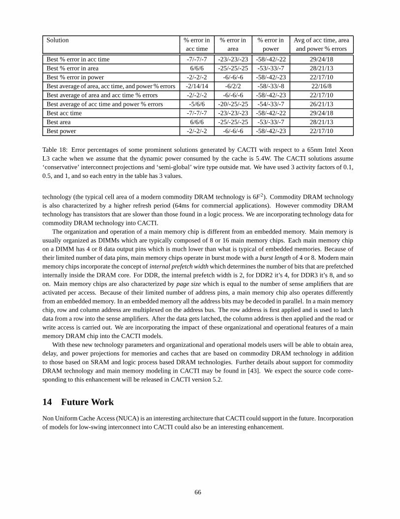
Solution % error in % error in % error in Avg of acc time, areaacc time area power and power % errors
Best % error in acc time -7/-7/-7 -23/-23/-23 -58/-42/-22 29/24/18Best % error in area 6/6/6 -25/-25/-25 -53/-33/-7 28/21/13Best % error in power -2/-2/-2 -6/-6/-6 -58/-42/-23 22/17/10Best average of area, acc time, and power % errors-2/14/14 -6/2/2 -58/-33/-8 22/16/8Best average of area and acc time % errors -2/-2/-2 -6/-6/-6 -58/-42/-23 22/17/10Best average of acc time and power % errors -5/6/6 -20/-25/-25 -54/-33/-7 26/21/13Best acc time -7/-7/-7 -23/-23/-23 -58/-42/-22 29/24/18Best area 6/6/6 -25/-25/-25 -53/-33/-7 28/21/13Best power -2/-2/-2 -6/-6/-6 -58/-42/-23 22/17/10
Table 18: Error percentages of some prominent solutions generated by CACTI with respect to a 65nm Intel XeonL3 cache when we assume that the dynamic power consumed by thecache is 5.4W. The CACTI solutions assume‘conservative’ interconnect projections and ‘semi-global’ wire type outside mat. We have used 3 activity factors of 0.1,0.5, and 1, and so each entry in the table has 3 values.
technology (the typical cell area of a modern commodity DRAMtechnology is 6F2). Commodity DRAM technologyis also characterized by a higher refresh period (64ms for commercial applications). However commodity DRAMtechnology has transistors that are slower than those foundin a logic process. We are incorporating technology data forcommodity DRAM technology into CACTI.
The organization and operation of a main memory chip is different from an embedded memory. Main memory isusually organized as DIMMs which are typically composed of 8or 16 main memory chips. Each main memory chipon a DIMM has 4 or 8 data output pins which is much lower than what is typical of embedded memories. Because oftheir limited number of data pins, main memory chips operatein burst mode with aburst lengthof 4 or 8. Modern mainmemory chips incorporate the concept ofinternal prefetch widthwhich determines the number of bits that are prefetchedinternally inside the DRAM core. For DDR, the internal prefetch width is 2, for DDR2 it’s 4, for DDR3 it’s 8, and soon. Main memory chips are also characterized bypage sizewhich is equal to the number of sense amplifiers that areactivated per access. Because of their limited number of address pins, a main memory chip also operates differentlyfrom an embedded memory. In an embedded memory all the address bits may be decoded in parallel. In a main memorychip, row and column address are multiplexed on the address bus. The row address is first applied and is used to latchdata from a row into the sense amplifiers. After the data gets latched, the column address is then applied and the read orwrite access is carried out. We are incorporating the impactof these organizational and operational features of a mainmemory DRAM chip into the CACTI models.
With these new technology parameters and organizational and operational models users will be able to obtain area,delay, and power projections for memories and caches that are based on commodity DRAM technology in additionto those based on SRAM and logic process based DRAM technologies. Further details about support for commodityDRAM technology and main memory modeling in CACTI may be found in [43]. We expect the source code corre-sponding to this enhancement will be released in CACTI version 5.2.
14 Future Work
Non Uniform Cache Access (NUCA) is an interesting architecture that CACTI could support in the future. Incorporationof models for low-swing interconnect into CACTI could also be an interesting enhancement.
66

15 Conclusions
In this technical report, we have described the various enhancements carried out in CACTI 5 while also providing acomprehensive overview of the CACTI area, access time and power modeling. CACTI 5 includes a number of majorimprovements over CACTI 4.0. The base technology modeling has been changed from simple linear scaling of theoriginal 0.8 micron technology to models based on the ITRS roadmap. Data for different ITRS device types has been in-corporated into CACTI. Interconnect technology data has also been updated so that it is now based off well-documentedmodels and data. CACTI 5 has also added support for modeling embedded DRAM in such a way that it now becomespossible to compare tradeoffs involving the use of embeddedSRAM or DRAM for identical input specifications. Thishas been achieved by an extensive rewrite of the CACTI code base. Various organizational and circuit assumptions havebeen clarified and updated. The modeling has also been restructured in such a way that it is now more modular andeasier to extend and evolve.
In the studies shown in this report, the impact of technologyassumptions on cache performance has been pointedout and emphasized. The importance of solution optimization techniques on memory and cache performance has alsobeen highlighted. Area, delay, and power results obtained from version 5.1 have been compared against published dataavailable for two prominent caches. Taking into account theextremely generic nature of CACTI, it was found that thereis reasonable agreement between the results produced by CACTI and the published data.
Finally, as in the original CACTI report, we would like to caution users against making too many conclusions basedon results shown in this report. It is important to know that CACTI is a simplified model for memories and caches withvarious limitations at the various levels of modeling, so appropriate caution and judgement needs to be exercised withits use. In general, it is best to use CACTI for studies that involve relative optimization.
Acknowledgments
We would like to thank the following people for many helpful discussions and comments: Al Davis from the Universityof Utah, and Jay Brockman and Christian Poellabauer from theUniversity of Notre Dame.
67

A Additional CACTI Validation Results for 90nm SPARC L2
Activity factor for dynamic power = 0.1
0
1
2
3
4
5
6
7
8
0 5 10 15
Power (W)
Acc
ess
tim
e (n
s)
CACTI generated solutions
Target SPARC L2
Activity factor for dynamic power = 0.5
0
1
2
3
4
5
6
7
8
0 5 10 15
Power (W)
Acc
ess
tim
e (n
s)
CACTI generated solutions
Target SPARC L2
Activity factor for dynamic power = 1.0
0
1
2
3
4
5
6
7
8
0 5 10 15
Power (W)
Acc
ess
tim
e (n
s)
CACTI generated solutions
Target SPARC L2
Figure 55: Access time, area and power of the 90nm SPARC L2 cache and of solutions generated by CACTI. TheCACTI solutions are for assumptions of ‘fast’ access mode, ‘conservative’ interconnect projections and ‘global’ wiretype outside mat. The 3 plots correspond to 3 activity factors assumed while computing dynamic power for the CACTI-generated solutions.
Solution % error in % error in % error in Avg of acc time, areaacc time area power and power % errors
Best % error in acc time -15/-15/-15 -13/-13/-13 -68/-54/-36 32/27/21Best % error in area -8/-8/-8 -16/-16/-16 -69/-54/-34 31/26/20Best % error in power -8/-15/-15 -16/1/1 -69/-56/-39 31/24/18Best average of area, acc time, and power % er-rors
-15/-15/-15 1/1/1 -69/-56/-39 28/24/18
Best average of area and acc time % errors -15/-15/-15 1/1/1 -69/-56/-39 28/24/18Best average of acc time and power % errors 6/6/6 26/26/26 -65/-48/-26 32/27/19Best acc time -15/-15/-15 -13/-13/-13 -68/-54/-36 32/27/21Best area -8/-8/-8 -16/-16/-16 -69/-54/-34 31/26/20Best power -8/-15/-15 -16/1/1 -69/-56/-39 31/24/18
Table 19: Error percentages of some prominent solutions generated by CACTI with respect to a 90nm SPARC L2 cacheunder assumptions of ‘fast’ access mode, ‘conservative’ interconnect projections and ‘global’ wire type outside mat.Wehave used 3 activity factors of 0.1, 0.5 and 1, and so each entry in the table has 3 values.
68

Activity factor for dynamic power = 0.1
0 1 2 3 4 5 6 7 8 9
10
0 5 10 15
Power (W)
Acc
ess
tim
e (n
s)
CACTI generated solutions
Target SPARC L2
Activity factor for dynamic power = 0.5
0 1 2 3 4 5 6 7 8 9
10
0 5 10 15
Power (W)
Acc
ess
tim
e (n
s)
CACTI generated solutions
Target SPARC L2
Activity factor for dynamic power = 1.0
0 1 2 3 4 5 6 7 8 9
10
0 5 10 15
Power (W)
Acc
ess
tim
e (n
s)
CACTI generated solutions
Target SPARC L2
Figure 56: Access time, area and power of the 90nm SPARC L2 cache and of solutions generated by CACTI. The CACTIsolutions are for assumptions of ‘normal’ access mode, ‘conservative’ interconnect projections and ‘semi-global’ wiretype outside mat. The 3 plots correspond to 3 activity factors assumed while computing dynamic power for the CACTI-generated solutions.
Solution % error in % error in % error in Avg of acc time, areaacc time area power and power % errors
Best % error in acc time 39/39/39 -39/-39/-39 -70/-64/-56 49/47/45Best % error in area 39/39/39 -39/-39/-39 -70/-64/-56 49/47/45Best % error in power 53/53/53 -37/-37/-37 -72/-66/-59 54/52/50Best average of area, acc time and power % errors39/39/39 -39/-39/-39 -70/-64/-56 49/47/45Best average of area and acc time % errors 39/39/39 -39/-39/-39 -70/-64/-56 49/47/45Best average of acc time and power % errors 39/39/39 -39/-39/-39 -70/-64/-56 49/47/45Best acc time 39/39/39 -39/-39/-39 -70/-64/-56 49/47/45Best area 39/39/39 -39/-39/-39 -70/-64/-56 49/47/45Best power 53/53/53 -37/-37/-37 -72/-66/-59 54/52/50
Table 20: Error percentages of some prominent solutions generated by CACTI with respect to a 90nm SPARC L2 cachefor a normal cache under assumptions of ‘normal’ access mode, ‘conservative’ interconnect projections and ‘semi-global’ wire type outside mat. The CACTI solutions and errors depends on the activity factor. We have used 3 activityfactors of 0.1, 0.5 and 1, and so each entry in the table has 3 values.
69

Activity factor for dynamic power = 0.1
0
1
2
3
4
5
6
7
8
0 5 10 15
Power (W)
Acc
ess
tim
e (n
s)
CACTI generated solutions
Target SPARC L2
Activity factor for dynamic power = 0.5
0
1
2
3
4
5
6
7
8
0 5 10 15
Power (W)
Acc
ess
tim
e (n
s)
CACTI generated solutions
Target SPARC L2
Activity factor for dynamic power = 1.0
0
1
2
3
4
5
6
7
8
0 5 10 15
Power (W)
Acc
ess
tim
e (n
s)
CACTI generated solutions
Target SPARC L2
Figure 57: Access time, area and power of the 90nm SPARC L2 cache and of solutions generated by CACTI. TheCACTI solutions are for assumptions of ‘normal’ access mode, ‘conservative’ interconnect projections and ‘global’wire type outside mat. The 3 plots correspond to 3 activity factors assumed while computing dynamic power for theCACTI-generated solutions.
Solution % error in % error in % error in Avg of acc time, areaacc time area power and power % errors
Best % error in acc time 12/12/12 -31/-31/-31 -70/-64/-56 38/36/33Best % error in area 23/23/23 -33/-33/-33 -72/-66/-57 43/41/38Best % error in power 23/22/22 -33/-27/-27 -72/-67/-60 43/39/37Best average of area, acc time and power % errors12/12/12 -31/-31/-31 -70/-64/-56 38/36/33Best average of area and acc time % errors 12/12/12 -31/-31/-31 -70/-64/-56 38/36/33Best average of acc time and power % errors 12/12/12 -31/-31/-31 -70/-64/-56 38/36/33Best acc time 12/12/12 -31/-31/-31 -70/-64/-56 38/36/33Best area 23/23/23 -33/-33/-33 -72/-66/-57 43/41/38Best power 23/22/22 -33/-27/-27 -72/-67/-60 43/39/37
Table 21: Error percentages of some prominent solutions generated by CACTI with respect to a 90nm SPARC L2 cachefor a normal cache under assumptions of ‘normal’ access mode, ‘conservative’ interconnect projections and ‘global’wire type outside mat. We have used 3 activity factors of 0.1,0.5 and 1, and so each entry in the table has 3 values.
70
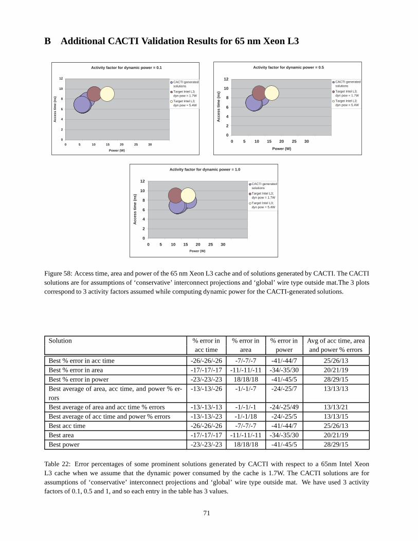
B Additional CACTI Validation Results for 65 nm Xeon L3
Activity factor for dynamic power = 0.1
0
2
4
6
8
10
12
0 5 10 15 20 25 30
Power (W)
Acc
ess
tim
e (n
s)
CACTI generated solutions
Target Intel L3; dyn pow = 1.7W
Target Intel L3; dyn pow = 5.4W
Activity factor for dynamic power = 0.5
0
2
4
6
8
10
12
0 5 10 15 20 25 30
Power (W)
Acc
ess
tim
e (n
s)
CACTI generated solutions
Target Intel L3; dyn pow = 1.7W
Target Intel L3; dyn pow = 5.4W
Activity factor for dynamic power = 1.0
0
2
4
6
8
10
12
0 5 10 15 20 25 30
Power (W)
Acc
ess
tim
e (n
s)
CACTI generated solutions
Target Intel L3; dyn pow = 1.7W
Target Intel L3; dyn pow = 5.4W
Figure 58: Access time, area and power of the 65 nm Xeon L3 cache and of solutions generated by CACTI. The CACTIsolutions are for assumptions of ‘conservative’ interconnect projections and ‘global’ wire type outside mat.The 3 plotscorrespond to 3 activity factors assumed while computing dynamic power for the CACTI-generated solutions.
Solution % error in % error in % error in Avg of acc time, areaacc time area power and power % errors
Best % error in acc time -26/-26/-26 -7/-7/-7 -41/-44/7 25/26/13Best % error in area -17/-17/-17 -11/-11/-11 -34/-35/30 20/21/19Best % error in power -23/-23/-23 18/18/18 -41/-45/5 28/29/15Best average of area, acc time, and power % er-rors
-13/-13/-26 -1/-1/-7 -24/-25/7 13/13/13
Best average of area and acc time % errors -13/-13/-13 -1/-1/-1 -24/-25/49 13/13/21Best average of acc time and power % errors -13/-13/-23 -1/-1/18 -24/-25/5 13/13/15Best acc time -26/-26/-26 -7/-7/-7 -41/-44/7 25/26/13Best area -17/-17/-17 -11/-11/-11 -34/-35/30 20/21/19Best power -23/-23/-23 18/18/18 -41/-45/5 28/29/15
Table 22: Error percentages of some prominent solutions generated by CACTI with respect to a 65nm Intel XeonL3 cache when we assume that the dynamic power consumed by thecache is 1.7W. The CACTI solutions are forassumptions of ‘conservative’ interconnect projections and ‘global’ wire type outside mat. We have used 3 activityfactors of 0.1, 0.5 and 1, and so each entry in the table has 3 values.
71

Solution % error in % error in % error in Avg of acc time, areaacc time area power and power % errors
Best % error in acc time -26/-26/-26 -7/-7/-7 -59/-44/-26 31/26/20Best % error in area -17/-17/-17 -11/-11/-11 -54/-35/-10 27/21/13Best % error in power -23/-23/-23 18/18/18 -60/-45/-27 34/29/23Best average of area, acc time and power % er-rors
-13/-13/-13 -1/-1/-1 -48/-25/3 21/13/6
Best average of area and acc time % errors -13/-13/-13 -1/-1/-1 -48/-25/3 21/13/6Best average of acc time and power % errors -13/-13/-13 -1/-1/-1 -48/-25/3 21/13/6Best acc time -26/-26/-26 -7/-7/-7 -59/-44/-26 31/26/20Best area -17/-17/-17 -11/-11/-11 -54/-35/-10 27/21/13Best power -23/-23/-23 18/18/18 -60/-45/-27 34/29/23
Table 23: Error percentages of some prominent solutions generated by CACTI with respect to a 65nm Intel XeonL3 cache when we assume that the dynamic power consumed by thecache is 5.4W. The CACTI solutions are forassumptions of ‘conservative’ interconnect projections and ‘global’ wire type outside mat. We have used 3 activityfactors of 0.1, 0.5 and 1, and so each entry in the table has 3 values.
72

References
[1] S. Alexenian, “Multi-level Semiconductor Memory Architecture and Method of Forming the Same,”US Patent 20050041513,Feb 2005.
[2] B. S. Amrutur and M. A. Horowitz, “Speed and Power Scalingof SRAM’s,” IEEE Journal of Solid-State Circuits, vol. 35, no. 2,pp. 175–185, Feb 2000.
[3] ——, “Fast Low Power Decoders for RAMs,”IEEE Journal of Solid-State Circuits, vol. 36, no. 10, pp. 1506–1515, Oct 2001.
[4] P. Bai,et al., “A 65nm Logic Technology Featuring 35nm Gate Lengths, Enhanced Channel Strain, 8 Cu Interconnect Layers,Low-k ILD and 0.57 micron2 SRAM cell,” in IEEE International Electron Devices Meeting, Dec 2004.
[5] J. Barth, J. Dreibelbis, E. Nelson, D. Anand, G. Pomichter, P. Jakobsem, M. Nelms, J. Leach, and G. Belansek, “EmbeddedDRAM design and architecture for the IBM 0.11-micron ASIC offering,” IBM Journal of Research and Development, vol. 46,no. 6, Nov 2002.
[6] J. Barth,et al., “A 500MHz random cycle 1.5ns-latency SOI embedded DRAM macro featuring a 3T micro sense amplifier,” inInternational Solid-State Circuits Conference, San Francisco, CA, Feb 2007.
[7] J. Chang,et al., “The 65-nm 16-MB Shared On-Die L3 Cache for the Dual-Core Intel Xeon Processor 7100 Series,”IEEEJournal of Solid-State Circuits, vol. 42, no. 4, Apr 2007.
[8] L. Chang,et al., “Stable SRAM cell design for the 32 nm node and beyond,” inSymposium on VLSI, 2005.
[9] J. Gilbert, S. Hunt, D. Gunadi, and G. Srinivasa, “TULSA,A Dual P4 Core Large Shared Cache Intel Xeon Processor for theMP Server Market Segment,” inHot Chips, Aug 2006.
[10] A. Hajimiri and R. Heald, “Design Issues in Cross-coupled Sense Amplifier,” inInternational Symposium on Circuits andSystems, May/Jun 1998, pp. 149–152.
[11] R. Ho, “On-chip Wires: Scaling and Efficiency,” Ph.D. dissertation, Stanford University, 2003.
[12] T. Hook, M. Breitwisch, J. Brown, P. Cottrell, D. Hoyniak, C. Lam, and R. Mann, “Noise margin and leakage in ultra-lowleakage SRAM cell design,”IEEE Transactions on Electron Devices, vol. 49, no. 8, Aug 2002.
[13] M. Horowitz, R. Ho, and K. Mai, “The Future of Wires,” In Invited Workshop Paper for SRC Conference., Tech. Rep., 1999.
[14] S. S. Iyer, J. J. E. Barth, P. C. Parries, J. P. Norum, J. P.Rice, L. R. Logan, and D. Hoyniak, “Embedded DRAM: Technologyplatform for the Blue Gene/L chip,”IBM Journal of Research and Development, vol. 49, no. 2/3, pp. 333–350, Mar/May 2005.
[15] J. J. Barth,et al., “A 500-MHz multi-banked compilable DRAM macro with directwrite and programmable pipelining,”IEEEJournal of Solid-State Circuits, vol. 40, no. 1, Jan 2005.
[16] S. Jin, J. Yi, J. Choi, D. Kang, Y. Park, and H. Min, “Prediction of data retention time distribution of DRAM by physics-basedstatistical simulation,”IEEE Transactions on Electron Devices, vol. 52, no. 11, Nov 2005.
[17] B. Keeth and R. Baker,DRAM Circuit Design: A Tutorial. IEEE Press, 2000.
[18] T. Kirihata, et al., “An 800-MHz embedded DRAM with a concurrent refresh mode,”IEEE Journal of Solid-State Circuits,vol. 40, no. 6, Jun 2005.
[19] V. Klee, et al., “A 0.13-micron logic-based embedded DRAM technology withelectrical fuses, Cu interconnect in SiLKTM,sub-7ns random access time and its extension to the 0.10-micron generation,” inIEEE International Electron Devices Meeting,2001.
[20] M. Mamidipaka and N. Dutt, “eCACTI: An Enhanced Power Estimation Model for On-chip Caches,” Center for EmbeddedComputer Systems (CECS), Tech. Rep. TR-04-28, 2004.
[21] M. Mamidipaka, K. Khouri, N. Dutt, and M. Abadir, “Analytical Models for Leakage Power Estimation of Memory ArrayStructures,” inProceedings of the 2nd IEEE/ACM/IFIP international conference on Hardware/software codesign and systemsynthesis, Sep 2004.
[22] R. Mann,et al., “Ultralow-power SRAM technology,”IBM Journal of Research and Development, vol. 47, no. 5/6, Sep/Nov2003.
[23] R. Matick and S. Schuster, “Logic-based eDRAM: Originsand rationale for use,”IBM Journal of Research and Development,vol. 49, no. 1, Jan 2005.
[24] Y. Matsubara,et al., “Fully integration of high density embedded DRAM with 65 nmCMOS technology (CMOS5),” inIEEEInternational Electron Devices Meeting, 2003.
73

[25] H. McIntyre, et al., “A 4-MB On-Chip L2 Cache for a 90-nm 1.6-GHz 64-bit Microprocessor,”IEEE Journal of Solid-StateCircuits, vol. 40, no. 1, Jan 2005.
[26] M. Na, E. Nowak, W. Haensch, and J. Cai, “The effective drive current of CMOS inverters,” inIEEE International ElectronDevices Meeting, Dec 2002.
[27] K. Noh, Y. Choi, J. Joo, M. Kim, J. Jung, J. Lim, C. Lee, G. Kim, and M. Kim, “A 130nm 1.1V 143 MHz SRAM-likeembedded DRAM compiler with dual asymmetric bit line sensing scheme and quiet unselected IO scheme,” inSymposium onVLSI Circuits, 2004.
[28] M. Oka and M. Suzuoki, “Designing and Programming the Emotion Engine,”IEEE Micro, vol. 19, no. 6, pp. 20–28, 1999.
[29] J. M. Rabaey, A. Chandrakasan, and B. Nikolic,Digital Integrated Circuits, 2nd ed. Prentice Hall, 2003.
[30] G. Reinman and N. P. Jouppi, “CACTI 2.0: An Integrated Cache Timing and Power Model,” DEC WRL, Tech. Rep. technicalreport number 2000/7, 2000.
[31] Ron Ho, “Tutorial: Dealing with issues in VLSI interconnect scaling.” inInternational Solid-State Circuits Conference, 2007.
[32] S. Rusu, S. Tam, H. Muljono, D. Ayers, and J. Chang, “A Dual-Core Multi-Threaded Xeon Processor with 16MB L3 Cache,”in International Solid-State Circuits Conference, San Francisco, CA, Feb. 2006.
[33] S. Rusu,et al., “A 65-nm Dual-Core Multithreaded Xeon Processor With 16-MB L3 Cache,” IEEE Journal of Solid-StateCircuits, vol. 42, no. 1, Jan 2007.
[34] P. Saxena, N. Menezes, P. Cocchini, and D. Kirkpatrick,“The scaling challenge: can correct-by-construction help?” in Interna-tional Symposium on Physical Design, Apr 2003.
[35] Semiconductor Industries Association, “International Technology Roadmap for Semiconductors,” 2005, http://www.itrs.net/.
[36] ——, “Model for Assessment of CMOS Technologies and Roadmaps (MASTAR),” 2005, http://www.itrs.net/models.html.
[37] T. M. Service, “http://www.mosis.org.”
[38] P. Shivakumar and N. P. Jouppi, “CACTI 3.0: An Integrated Cache Timing, Power, and Area Model,” Hewlett Packard Labora-tories, Tech. Rep. WRL-2001-2, 2001.
[39] I. E. Sutherland, R. F. Sproull, and D. Harris,Logical Effort:Designing Fast CMOS Circuits, 1st ed. San Mateo, CA: MorganKaufmann, 1999.
[40] D. Tarjan, S. Thoziyoor, and N. P. Jouppi, “CACTI 4.0,” HP Labs, Tech. Rep. HPL-2006-86, 2006.
[41] J. M. Tendler, J. S. Dodson, J. J. S. Fields, H. Le, and B. Sinharoy, “POWER4 system microarchitecture,”IBM Journal ofResearch and Development, vol. 46, no. 1, pp. 5–26, Jan. 2002.
[42] S. Thompson, M. Alavi, M. Hussein, P. Jacaob, C. Kenyon,P. Moon, M. Prince, S. Sivakumar, S. Tyagi, and M. Bohr, “130nmLogic Technology Featuring 60nm Transistors, Low-K Dielectrics, and Cu Interconnects,”Intel Technical Journal, vol. 6, no. 2,May 2002.
[43] S. Thoziyoor, Ph.D. dissertation, University of NotreDame, 2008.
[44] R. Varada, M. Sriram, K. Chou, and J. Guzzo, “Design and Integration Methods for a Multi-threaded Dual Core 65nm XeonProcessor,” inInternational Conference on Computer-Aided Design, Nov 2006.
[45] G. Wang, P. Parries, B. Khan, J. Liu, Y. Otani, J. Norum, N. Robson, T. Kirihata, and S. Iyer, “A 0.168/0.11 micron2 highlyscalable high performance embedded DRAM cell for 90/65 nm logic applications,” inSymposium on VLSI Circuits, 2004.
[46] S. Wilton and N. Jouppi, “CACTI: An enhanced cache access and cycle time model,”IEEE Journal of Solid-State Circuits,vol. 31, no. 5, pp. 677–688, May 1996.
[47] S. Wilton and N. P. Jouppi, “An Enhanced Access and CycleTime Model for On-Chip Caches,” DEC WRL, Tech. Rep. technicalreport number 93/5, 1994.
[48] P. Yeh, D. Nayak, and D. Gitlin, “Improved CV/I methodology to accurately predict CMOS technology performane,”IEEETransactions on Electron Devices, vol. 54, no. 7, Jul 2007.
[49] H. Yoshida, K. De, and V. Boppana, “Accurate pre-layoutestimation of standard cell characteristics,” inProceedings of the 41stannual conference on Design automation. New York, NY, USA: ACM Press, 2004, pp. 208–211.
[50] W. Zhao and Y. Cao, “New Generation of Predictive Technology Model for Sub-45nm Design Exploration,” inIEEE Interna-tional Symposium on Quality Electronic Design, Mar 2006.
74


![Highlands Cacti (Native Southwest Cacti).ppt [Read-Only]Many species of cacti and other succulents are quite cold hardy. • Though cacti are often thought of as low desert plants,](https://static.fdocuments.in/doc/165x107/5e6f715b08e7e57abf396376/highlands-cacti-native-southwest-cactippt-read-only-many-species-of-cacti-and.jpg)


