Ca Bling! Pacificon 2011 Norcal Buildathon Project
12
Ca Bling! Pacificon 2011 Norcal Buildathon Project by W1REX / QRPme 10/23/2011 ver 1.1 www.QRPme.com The Ca Bling! Kit is a small Picaxe micro controller development board designed by W1REX as a project board for the Norcal buildathon session as part of Pacificon 2011. The board got its name from the initial program that was developed to show off its features: microcontroller based smarts, opto-coupled input trigger, ultra-bright LED, speaker and relay. The demonstration application, the Ca Bling! program, is designed to output a short message in Morse Code when triggered by a switch. The intention was to feed the board power from the rear tail light or license plate circuit and trigger the message transmission by tapping the brake pedal. The ultra- bright LED would then send a coded message to the following vehicle. Of course, you can write any program you want to work with the resources on the circuit board.
Transcript of Ca Bling! Pacificon 2011 Norcal Buildathon Project

Ca Bling!Pacificon 2011
Norcal Buildathon Project
by W1REX / QRPme
10/23/2011 ver 1.1
www.QRPme.com
The Ca Bling! Kit is a small Picaxe micro controller development boarddesigned by W1REX as a project board for the Norcal buildathon session aspart of Pacificon 2011. The board got its name from the initial program thatwas developed to show off its features: microcontroller based smarts,opto-coupled input trigger, ultra-bright LED, speaker and relay. Thedemonstration application, the Ca Bling! program, is designed to output ashort message in Morse Code when triggered by a switch. The intention wasto feed the board power from the rear tail light or license plate circuit andtrigger the message transmission by tapping the brake pedal. The ultra-bright LED would then send a coded message to the following vehicle. Ofcourse, you can write any program you want to work with the resources onthe circuit board.

Sort out the parts for a smooth build..

Now you should familiarize yourself with the schematic diagram of the CaBling! Circuitry.........

To BREAK or not to BREAK...
Now comes the maine question: Are you intending to put the Ca Bling! boardin some tiny little place where you need the absolute minimal board size?
The CaB board is scored on both the top & bottom sides just about in themiddle of the board. The scoring allows the board to be snapped in half. Theactual Picaxe micro & bling! circuitry is on the right half (in the abovepicture) while the downloading circuit and extra general purposedevelopment goodies are on the left half. Swiss pins can be soldered intothe double row of pads bordering the score line so that the boards can betemporarily connected for development or downloading purposes yet partedto preserve the tiny footprint of the actual bling! function. If you don'tthink that you will ever require the minimal footprint, you can skip theSwiss pins and simply bridge the 6 sets of pads with clipped leads frompreviously installed components or use the zero ohm jumpers supplied withthe kit.... and don't snap the board in half!

I've found that it is easiest to install all the Swiss pins first...
So I separate the strips of Swiss pins into single pins and populate the padsalong the score line. I also use some of the extra pins out at the furthestpads to add stability...then place a spare piece of pcb stock over the top.
Turn the 'sandwich' over and place it on the bench. If you add a little downpressure with your finger while you solder the pins, they should all come outfairly straight and even. Just remember which pins you want to solder...andwhich pins you added to enable the sandwich to lay flat and even whilesoldering...
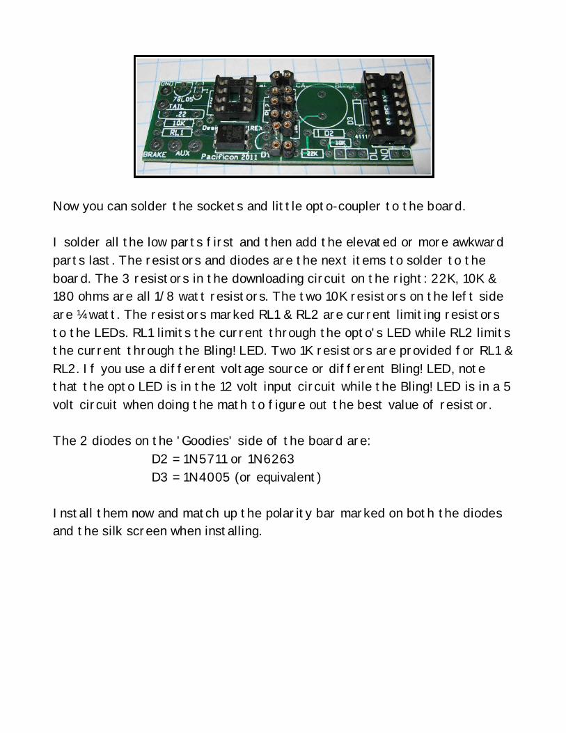
Now you can solder the sockets and little opto-coupler to the board.
I solder all the low parts first and then add the elevated or more awkwardparts last. The resistors and diodes are the next items to solder to theboard. The 3 resistors in the downloading circuit on the right: 22K, 10K &180 ohms are all 1/8 watt resistors. The two 10K resistors on the left sideare ¼ watt. The resistors marked RL1 & RL2 are current limiting resistorsto the LEDs. RL1 limits the current through the opto's LED while RL2 limitsthe current through the Bling! LED. Two 1K resistors are provided for RL1 &RL2. If you use a different voltage source or different Bling! LED, notethat the opto LED is in the 12 volt input circuit while the Bling! LED is in a 5volt circuit when doing the math to figure out the best value of resistor.
The 2 diodes on the 'Goodies' side of the board are:D2 = 1N5711 or 1N6263D3 = 1N4005 (or equivalent)
Install them now and match up the polarity bar marked on both the diodesand the silk screen when installing.

The 2 capacitors are next. You might have to re-bend the caps supplied inyour kit to fit the pad spacing. The initial stock of .1uf caps had .2” spacingfor .1” spaced pads so it should be re-bent like the left hand picture above.The .22uf cap has .1” spaced leads and needs to be widened for the .2”spaced pads. Bend it like the right hand picture. Install both caps.
The installation of the caps should look like the following pictures.

Now solder in the 78L05 voltage regulator.
Add the small round speaker to the 'goodies' side. The speaker has apolarity so solder the speaker in with the + marked pin nearest the centerof the pcb. The – pin is close to the edge of the board. You can tell the –pad on the bottom side of the pcb by its little 'star pattern' of tracesconnecting the pad to the ground plane. The 2 Molex style connectors (3 pinand 2 pin male headers) should now be installed. Now that most of thesoldering is done, you can install the micro and relay into their respectivesockets.
Your board should look like the picture above...
Solder in the ultra-bright LED to the pads marked D1. Note the polaritymarked on the pad with a flat side. Install the LED with flats matched.

Leave some height on the LED to allow jumpers to be installed/uninstalled.Basic Ca Bling! Operation only requires 3 jumpers to download new programsinto the micro but you might as well connect all 6 jumpers for testingpurposes.
The Ca Bling! Board requires 3 wires to operate. Ground comes into theboard at GND. The +12 volt supply comes into the board at TAIL while theCa Bling! trigger (switch) signal enters through BRAKE. Solder 3 wires tothose pads.

Unfortunately, the ground plane did not flow to well on the 'goodies' side ofthe board. A portion of the ground plane containing the speaker ground isisolated from the ground on the other half. Solder a short piece of hookupwire between the – speaker lead and the ground pin of the downloadingconnector as shown in the upper right picture.
I soldered a small computer front panel switch from my junk box to theAUX terminals to serve as an alternate switch for program development.
Your Ca Bling! Kit should now be ready to apply power to and download theCa Bling! Program. But you will need to make the downloading cable.

Here are the details for the cable:
The downloading cable can be made using an ‘old’ DB9F serial cable like theone pictured. Below. One end is cut off and 3 Molex pins are inserted on theTxd, Rxd and Ground (2,3 and 5) pins. Complete details for making bothSerial and USB downloading cables can be found at the Picaxe site:
< http://www.rev-ed.co.uk/docs/picaxe_manual3.pdf>
Use the link to the manual and go to Page 42 for cable info…
Green=groundRed & OrangeAre Tx & Rx
Mark the ground end to keep track when attaching to your project board.Mark the board ground too.

A homebrew download cable ready to go…
Check into the QRPme website:www.QRPme.com
OOPS! The following picture shows the Ca Bling! Board completed and readyfor some serious programming FUN....with 6 errors Can you spot them?