C70 Capacitor Bank Protection and Control System Instruction … · 2015-09-03 · GE Digital...
546
GE Digital Energy Instruction Manual Product version: 7.3x GE publication code: 1601-9015-AB2 (GEK-119614A) C70 Capacitor Bank Protection and Control System 1601-9015-AB2 LISTED 52TL IND.CONT. EQ. E83849
Transcript of C70 Capacitor Bank Protection and Control System Instruction … · 2015-09-03 · GE Digital...
GEDigital Energy
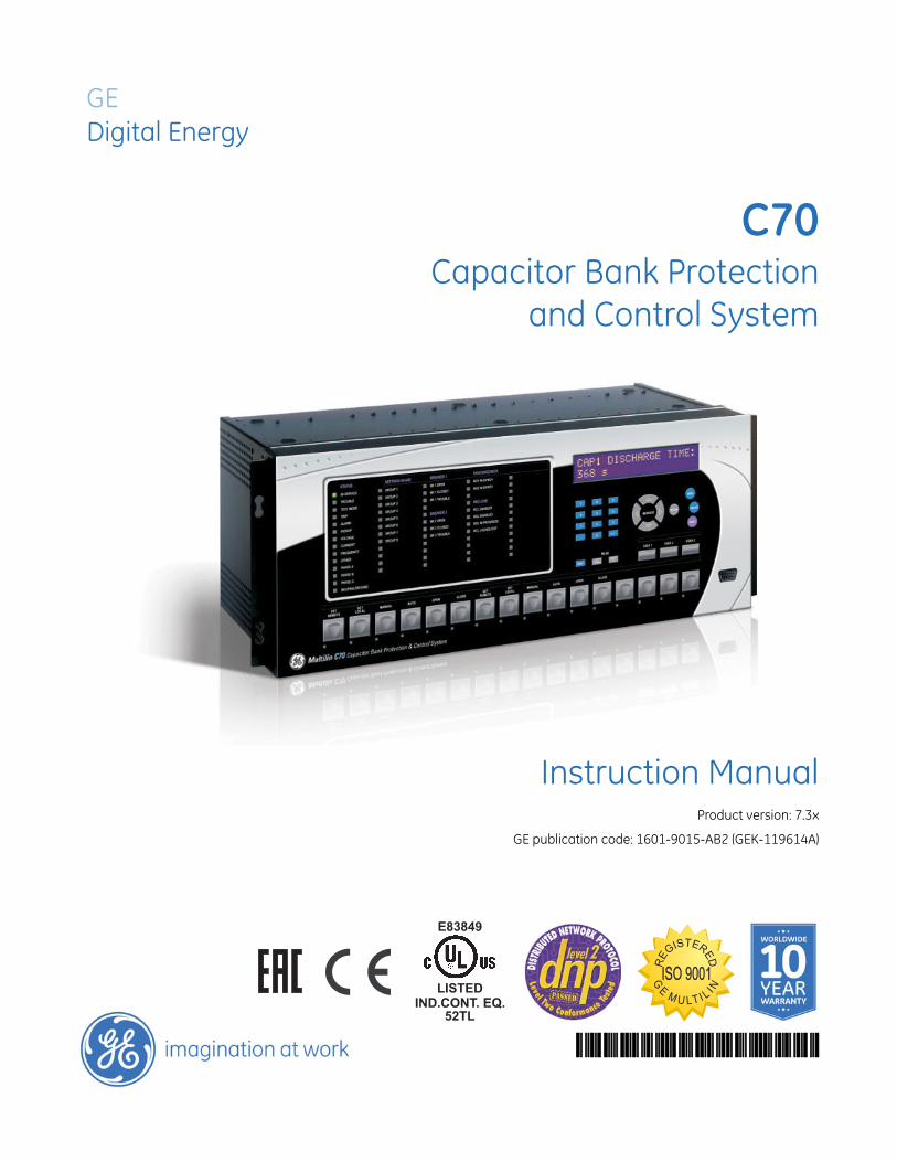
Instruction ManualProduct version: 7.3x
GE publication code: 1601-9015-AB2 (GEK-119614A)
C70Capacitor Bank Protection
and Control System
1601-9015-AB2
LISTED
52TL
IND.CONT. EQ.
E83849

Copyright © 2015 GE Multilin Inc. All rights reserved.
C70 Capacitor Bank Protection and Control System Instruction Manual for version 7.3x.
C70, FlexLogic, FlexElement, FlexCurve, FlexAnalog, FlexInteger, FlexState, EnerVista, CyberSentry, HardFiber, Digital Energy, Multilin, and GE Multilin are trademarks or registered trademarks of GE Multilin Inc.
The contents of this manual are the property of GE Multilin Inc. This documentation is furnished on license and may not be reproduced in whole or in part without the permission of GE Multilin. The content of this manual is for informational use only and is subject to change without notice.
Part number: 1601-9015-AB2 (September 2015)

C70 CAPACITOR BANK PROTECTION AND CONTROL SYSTEM – INSTRUCTION MANUAL iii
C70 Capacitor Bank Protection and Control System
Table of contents
1 INTRODUCTION 1.1 Safety symbols and definitions...................................................................... 1-11.1.1 General cautions and warnings ...................................................................................... 1-1
1.2 For further assistance ..................................................................................... 1-2
2 PRODUCT DESCRIPTION
2.1 Product description.......................................................................................... 2-12.2 Security .............................................................................................................. 2-32.3 Order codes ....................................................................................................... 2-7
2.3.1 Order codes with enhanced CT/VT modules............................................................. 2-82.3.2 Order codes with process bus modules ....................................................................2-102.3.3 Replacement modules.......................................................................................................2-12
2.4 Signal processing ...........................................................................................2-152.4.1 UR signal processing ..........................................................................................................2-15
2.5 Specifications ..................................................................................................2-172.5.1 Protection elements............................................................................................................2-172.5.2 User-programmable elements ......................................................................................2-222.5.3 Monitoring................................................................................................................................2-232.5.4 Metering....................................................................................................................................2-242.5.5 Inputs .........................................................................................................................................2-252.5.6 Power supply ..........................................................................................................................2-262.5.7 Outputs .....................................................................................................................................2-272.5.8 Communications ..................................................................................................................2-292.5.9 Inter-relay communications ...........................................................................................2-302.5.10 Environmental........................................................................................................................2-312.5.11 Type tests .................................................................................................................................2-322.5.12 Production tests ....................................................................................................................2-322.5.13 Approvals .................................................................................................................................2-332.5.14 Maintenance...........................................................................................................................2-33
3 INSTALLATION 3.1 Unpack and inspect ......................................................................................... 3-13.2 Panel cutouts .................................................................................................... 3-2
3.2.1 Horizontal units ....................................................................................................................... 3-23.2.2 Vertical units ............................................................................................................................. 3-33.2.3 Rear terminal layout ............................................................................................................. 3-8
3.3 Wiring ................................................................................................................. 3-9

iv C70 CAPACITOR BANK PROTECTION AND CONTROL SYSTEM – INSTRUCTION MANUAL
TABLE OF CONTENTS
3.3.1 Typical wiring............................................................................................................................3-93.3.2 Dielectric strength ...............................................................................................................3-103.3.3 Control power........................................................................................................................3-103.3.4 CT/VT modules ......................................................................................................................3-113.3.5 Process bus modules .........................................................................................................3-133.3.6 Contact inputs and outputs ............................................................................................3-133.3.7 Transducer inputs and outputs.....................................................................................3-203.3.8 RS232 faceplate port..........................................................................................................3-223.3.9 CPU communication ports ..............................................................................................3-223.3.10 IRIG-B.........................................................................................................................................3-24
3.4 Direct input and output communications .................................................3-253.4.1 Description..............................................................................................................................3-253.4.2 Fiber: LED and ELED transmitters.................................................................................3-273.4.3 G.703 interface......................................................................................................................3-273.4.4 RS422 interface.....................................................................................................................3-313.4.5 IEEE C37.94 interface .........................................................................................................3-33
3.5 Activate relay ..................................................................................................3-363.6 Install software ...............................................................................................3-37
3.6.1 EnerVista communication overview ...........................................................................3-373.6.2 System requirements.........................................................................................................3-383.6.3 Install software .....................................................................................................................3-38
3.7 Configure the C70 for software access ......................................................3-393.7.1 Configure serial communication ..................................................................................3-403.7.2 Configure Ethernet communication ...........................................................................3-413.7.3 Automatic discovery of UR devices.............................................................................3-42
3.8 Connect to the C70.........................................................................................3-423.8.1 Connect to the C70 in EnerVista ...................................................................................3-423.8.2 Use Quick Connect via the front panel RS232 port .............................................3-433.8.3 Use Quick Connect via a rear Ethernet port............................................................3-44
3.9 Set up CyberSentry and change default password..................................3-49
4 INTERFACES 4.1 EnerVista software interface.......................................................................... 4-14.1.1 Introduction...............................................................................................................................4-14.1.2 Settings files ..............................................................................................................................4-14.1.3 Event viewing............................................................................................................................4-24.1.4 File support ................................................................................................................................4-24.1.5 EnerVista main window .......................................................................................................4-24.1.6 Settings templates .................................................................................................................4-34.1.7 Secure and lock FlexLogic equations ............................................................................4-84.1.8 Settings file traceability.....................................................................................................4-10
4.2 Front panel interface .....................................................................................4-124.2.1 Front panel display..............................................................................................................4-124.2.2 Front panel keypad.............................................................................................................4-124.2.3 Menu navigation ..................................................................................................................4-134.2.4 Menu hierarchy.....................................................................................................................4-134.2.5 Changing settings................................................................................................................4-144.2.6 Faceplate .................................................................................................................................4-154.2.7 LED indicators........................................................................................................................4-174.2.8 Custom LED labeling ..........................................................................................................4-204.2.9 Breaker control .....................................................................................................................4-254.2.10 Change passwords .............................................................................................................4-264.2.11 Invalid password entry......................................................................................................4-27
4.3 Logic diagrams ...............................................................................................4-28
TABLE OF CONTENTS
C70 CAPACITOR BANK PROTECTION AND CONTROL SYSTEM – INSTRUCTION MANUAL v
5 SETTINGS 5.1 Settings menu ................................................................................................... 5-15.2 Overview ............................................................................................................ 5-4
5.2.1 Introduction to elements .................................................................................................... 5-45.2.2 Introduction to AC sources ................................................................................................ 5-5
5.3 Product setup.................................................................................................... 5-75.3.1 Security ....................................................................................................................................... 5-75.3.2 Display properties ................................................................................................................5-255.3.3 Clear relay records ..............................................................................................................5-275.3.4 Communications ..................................................................................................................5-275.3.5 Modbus user map ................................................................................................................5-825.3.6 Real-time clock......................................................................................................................5-825.3.7 User-programmable fault report..................................................................................5-865.3.8 Oscillography .........................................................................................................................5-875.3.9 Data logger .............................................................................................................................5-895.3.10 User-programmable LEDs ...............................................................................................5-905.3.11 User-programmable self tests .......................................................................................5-945.3.12 Control pushbuttons ...........................................................................................................5-945.3.13 User-programmable pushbuttons...............................................................................5-965.3.14 Flex state parameters .....................................................................................................5-1015.3.15 User-definable displays..................................................................................................5-1025.3.16 Direct inputs and outputs..............................................................................................5-1045.3.17 Installation............................................................................................................................5-111
5.4 Remote resources ........................................................................................5-1115.4.1 Remote resources configuration ...............................................................................5-111
5.5 System setup.................................................................................................5-1125.5.1 AC inputs ...............................................................................................................................5-1125.5.2 Power system......................................................................................................................5-1145.5.3 Signal sources.....................................................................................................................5-1145.5.4 Breakers.................................................................................................................................5-1175.5.5 Disconnect switches ........................................................................................................5-1225.5.6 FlexCurves ............................................................................................................................5-125
5.6 FlexLogic ........................................................................................................5-1325.6.1 FlexLogic operands ..........................................................................................................5-1325.6.2 FlexLogic rules ....................................................................................................................5-1455.6.3 FlexLogic evaluation ........................................................................................................5-1455.6.4 FlexLogic example ............................................................................................................5-1465.6.5 FlexLogic equation editor ..............................................................................................5-1515.6.6 FlexLogic timers .................................................................................................................5-1515.6.7 FlexElements .......................................................................................................................5-1515.6.8 Non-volatile latches .........................................................................................................5-155
5.7 Grouped elements........................................................................................5-1565.7.1 Overview................................................................................................................................5-1565.7.2 Setting group 1...................................................................................................................5-1565.7.3 Phase current......................................................................................................................5-1575.7.4 Neutral current...................................................................................................................5-1715.7.5 Ground current...................................................................................................................5-1835.7.6 Negative sequence current..........................................................................................5-1855.7.7 Breaker failure (ANSI 50BF) ...........................................................................................5-1915.7.8 Voltage elements...............................................................................................................5-200
5.8 Control elements ..........................................................................................5-2175.8.1 Overview................................................................................................................................5-2175.8.2 Trip bus...................................................................................................................................5-2175.8.3 Setting groups.....................................................................................................................5-2195.8.4 Selector switch ...................................................................................................................5-2205.8.5 Time of day timers ............................................................................................................5-227

vi C70 CAPACITOR BANK PROTECTION AND CONTROL SYSTEM – INSTRUCTION MANUAL
TABLE OF CONTENTS
5.8.6 Capacitor control .............................................................................................................. 5-2285.8.7 Automatic voltage regulator ....................................................................................... 5-2335.8.8 Digital elements................................................................................................................. 5-2375.8.9 Digital counters.................................................................................................................. 5-2405.8.10 Monitoring elements ....................................................................................................... 5-242
5.9 Inputs/outputs ..............................................................................................5-2545.9.1 Contact inputs .................................................................................................................... 5-2545.9.2 Virtual inputs ....................................................................................................................... 5-2565.9.3 Contact outputs................................................................................................................. 5-2575.9.4 Virtual outputs.................................................................................................................... 5-2605.9.5 Resetting ............................................................................................................................... 5-2605.9.6 Direct inputs and outputs ............................................................................................. 5-261
5.10 Transducer inputs/outputs.........................................................................5-2655.10.1 DCmA inputs ....................................................................................................................... 5-2655.10.2 RTD inputs ............................................................................................................................ 5-2665.10.3 DCmA outputs .................................................................................................................... 5-267
5.11 Testing ............................................................................................................5-2705.11.1 Test mode function .......................................................................................................... 5-2705.11.2 Test mode forcing............................................................................................................. 5-2715.11.3 Force contact inputs ....................................................................................................... 5-2725.11.4 Force contact outputs .................................................................................................... 5-272
6 ACTUAL VALUES 6.1 Actual values menu.......................................................................................... 6-16.2 Status.................................................................................................................. 6-3
6.2.1 Contact inputs ..........................................................................................................................6-36.2.2 Virtual inputs .............................................................................................................................6-36.2.3 RxGOOSE boolean inputs ....................................................................................................6-36.2.4 RxGOOSE DPS inputs.............................................................................................................6-46.2.5 Contact outputs.......................................................................................................................6-46.2.6 Virtual outputs..........................................................................................................................6-46.2.7 RxGOOSE status.......................................................................................................................6-46.2.8 RxGOOSE statistics.................................................................................................................6-56.2.9 Digital counters........................................................................................................................6-56.2.10 Selector switches ....................................................................................................................6-56.2.11 Time of day timers..................................................................................................................6-66.2.12 Flex States ..................................................................................................................................6-66.2.13 Ethernet.......................................................................................................................................6-66.2.14 Real time clock synchronizing ..........................................................................................6-66.2.15 Direct inputs ..............................................................................................................................6-76.2.16 Direct devices status .............................................................................................................6-86.2.17 Remaining connection status ...........................................................................................6-86.2.18 Parallel Redundancy Protocol (PRP) ...............................................................................6-9
6.3 Metering ............................................................................................................. 6-96.3.1 Metering conventions ...........................................................................................................6-96.3.2 Sources .....................................................................................................................................6-136.3.3 Capacitor control .................................................................................................................6-176.3.4 Capacitor bank......................................................................................................................6-186.3.5 Tracking frequency .............................................................................................................6-196.3.6 FlexElements ..........................................................................................................................6-196.3.7 RxGOOSE analogs................................................................................................................6-196.3.8 Transducer inputs/outputs..............................................................................................6-20
6.4 Records.............................................................................................................6-206.4.1 User-programmable fault reports ...............................................................................6-206.4.2 Event records.........................................................................................................................6-206.4.3 Oscillography .........................................................................................................................6-21
TABLE OF CONTENTS
C70 CAPACITOR BANK PROTECTION AND CONTROL SYSTEM – INSTRUCTION MANUAL vii
6.4.4 Data logger .............................................................................................................................6-216.5 Product information ......................................................................................6-22
6.5.1 Model information................................................................................................................6-226.5.2 Firmware revisions ..............................................................................................................6-22
7 COMMANDS AND TARGETS
7.1 Commands menu ............................................................................................. 7-17.1.1 Capacitor bank automatic setting ................................................................................. 7-27.1.2 Virtual inputs ............................................................................................................................ 7-67.1.3 Clear records ............................................................................................................................ 7-67.1.4 Set date and time................................................................................................................... 7-77.1.5 Relay maintenance................................................................................................................ 7-77.1.6 Security ....................................................................................................................................... 7-8
7.2 Targets menu .................................................................................................... 7-97.2.1 Target messages.................................................................................................................... 7-97.2.2 Relay self-tests ........................................................................................................................ 7-9
8 APPLICATION OF SETTINGS
8.1 Arrangement of shunt capacitor banks....................................................... 8-18.1.1 Overview..................................................................................................................................... 8-18.1.2 Externally fused capacitors ............................................................................................... 8-18.1.3 Internally fused capacitors ................................................................................................ 8-28.1.4 Fuseless capacitors............................................................................................................... 8-28.1.5 Unfused capacitors ............................................................................................................... 8-3
8.2 Connections of shunt capacitor banks......................................................... 8-38.2.1 Grounded wye-connected banks ................................................................................... 8-38.2.2 Ungrounded wye-connected banks.............................................................................. 8-38.2.3 Delta connected banks........................................................................................................ 8-48.2.4 H-configuration....................................................................................................................... 8-48.2.5 Tapped configuration........................................................................................................... 8-48.2.6 Summary.................................................................................................................................... 8-4
8.3 Protection methods for capacitor banks ..................................................... 8-58.3.1 Overview..................................................................................................................................... 8-58.3.2 Capacitor unbalance protection..................................................................................... 8-58.3.3 Protection for rack faults (arc-over within capacitor banks) ...........................8-108.3.4 Overvoltage.............................................................................................................................8-108.3.5 Overcurrent.............................................................................................................................8-118.3.6 Loss of bus voltage..............................................................................................................8-11
8.4 Settings example ............................................................................................8-118.4.1 Overview...................................................................................................................................8-118.4.2 VT and CT setup ....................................................................................................................8-128.4.3 Source assignment..............................................................................................................8-138.4.4 Bank unbalance calculations .........................................................................................8-148.4.5 Bank voltage differential settings.................................................................................8-168.4.6 Bank phase current unbalance settings ...................................................................8-188.4.7 Bank phase overvoltage settings .................................................................................8-198.4.8 Bank phase undervoltage settings ..............................................................................8-208.4.9 Bank overcurrent protection...........................................................................................8-21
9 THEORY OF OPERATION
9.1 Overview ............................................................................................................ 9-19.1.1 General operation.................................................................................................................. 9-19.1.2 Bank phase overvoltage (ANSI 59B) .............................................................................. 9-19.1.3 Voltage differential (ANSI 87V) ......................................................................................... 9-39.1.4 Compensated bank neutral voltage unbalance (ANSI 59NU) ........................... 9-79.1.5 Phase current unbalance (ANSI 60P)...........................................................................9-10

viii C70 CAPACITOR BANK PROTECTION AND CONTROL SYSTEM – INSTRUCTION MANUAL
TABLE OF CONTENTS
9.1.6 Neutral current unbalance (ANSI 60N).......................................................................9-13
10 MAINTENANCE 10.1 General maintenance ....................................................................................10-110.1.1 In-service maintenance....................................................................................................10-110.1.2 Out-of-service maintenance ..........................................................................................10-110.1.3 Unscheduled maintenance (system interruption) ................................................10-2
10.2 Back up and restore settings .......................................................................10-210.2.1 Back up settings ...................................................................................................................10-210.2.2 Restore settings....................................................................................................................10-3
10.3 Upgrade firmware ..........................................................................................10-410.4 Upgrade software...........................................................................................10-510.5 Replace module ..............................................................................................10-610.6 Battery..............................................................................................................10-7
10.6.1 Replace battery for RH/RL power supply .................................................................10-710.6.2 Replace battery for SH/SL power supply..................................................................10-810.6.3 Dispose of battery ...............................................................................................................10-9
10.7 Clear files and data after uninstall ...........................................................10-1210.8 Repairs............................................................................................................10-1310.9 Storage ...........................................................................................................10-1310.10Disposal..........................................................................................................10-13
A FLEXANALOG OPERANDS
A.1 FlexAnalog items .............................................................................................A-1
B RADIUS SERVER CONFIGURATION
B.1 RADIUS server configuration .........................................................................B-1
C MISCELLANEOUS C.1 Warranty ...........................................................................................................C-1C.2 Revision history ................................................................................................C-1
ABBREVIATIONS
INDEX

C70 CAPACITOR BANK PROTECTION AND CONTROL SYSTEM – INSTRUCTION MANUAL 1-1
C70 Capacitor Bank Protection and Control System
Chapter 1: Introduction
Introduction
This chapter outlines safety and technical support information.
1.1 Safety symbols and definitionsBefore attempting to install or use the device, review all safety indicators in this document to help prevent injury, equipment damage, or downtime.
The following safety and equipment symbols are used in this document.
1.1.1 General cautions and warningsThe following general safety precautions and warnings apply.
Follow the requirements of this manual, including adequate wiring size and type, terminal torque settings, voltage, current magnitudes applied, and adequate isolation/clearance in external wiring from high to low voltage circuits.Use the device only for its intended purpose and application.Ensure that all ground paths are uncompromised for safety purposes during device operation and service.Ensure that the control power applied to the device, the AC current, and voltage input match the ratings specified on the relay nameplate. Do not apply current or voltage in excess of the specified limits.
Indicates a hazardous situation which, if not avoided, will result in death or serious injury.
Indicates a hazardous situation which, if not avoided, could result in death or serious injury.
Indicates a hazardous situation which, if not avoided, could result in minor or moderate injury.
Indicates practices not related to personal injury.
Ensure that all connections to the product are correct so as to avoid accidental risk of shock and/or fire, for example such as can arise from high voltage connected to low voltage terminals.

1-2 C70 CAPACITOR BANK PROTECTION AND CONTROL SYSTEM – INSTRUCTION MANUAL
FOR FURTHER ASSISTANCE CHAPTER 1: INTRODUCTION
1Only qualified personnel are to operate the device. Such personnel must be thoroughly familiar with all safety cautions and warnings in this manual and with applicable country, regional, utility, and plant safety regulations.Hazardous voltages can exist in the power supply and at the device connection to current transformers, voltage transformers, control, and test circuit terminals. Make sure all sources of such voltages are isolated prior to attempting work on the device.Hazardous voltages can exist when opening the secondary circuits of live current transformers. Make sure that current transformer secondary circuits are shorted out before making or removing any connection to the current transformer (CT) input terminals of the device.For tests with secondary test equipment, ensure that no other sources of voltages or currents are connected to such equipment and that trip and close commands to the circuit breakers or other switching apparatus are isolated, unless this is required by the test procedure and is specified by appropriate utility/plant procedure.When the device is used to control primary equipment, such as circuit breakers, isolators, and other switching apparatus, all control circuits from the device to the primary equipment must be isolated while personnel are working on or around this primary equipment to prevent any inadvertent command from this device.Use an external disconnect to isolate the mains voltage supply.
1.2 For further assistanceFor product support, contact the information and call center as follows:
GE Digital Energy650 Markland StreetMarkham, OntarioCanada L6C 0M1Worldwide telephone: +1 905 927 7070Europe/Middle East/Africa telephone: +34 94 485 88 54North America toll-free: 1 800 547 8629Fax: +1 905 927 5098Worldwide e-mail: [email protected] e-mail: [email protected]: http://www.gedigitalenergy.com/multilin
LED transmitters are classified as IEC 60825-1 Accessible Emission Limit (AEL) Class 1M. Class 1M devices are considered safe to the unaided eye. Do not view directly with optical instruments.
This product is rated to Class A emissions levels and is to be used in Utility, Substation Industrial environments. Not to be used near electronic devices rated for Class B levels.
C70 CAPACITOR BANK PROTECTION AND CONTROL SYSTEM – INSTRUCTION MANUAL 2-1
C70 Capacitor Bank Protection and Control System
Chapter 2: Product description
Product description
This chapter outlines the product, order codes, and specifications.
2.1 Product descriptionThe C70 Capacitor Bank Protection and Control System is part of the Universal Relay (UR) series of products. It is a microprocessor-based relay for protection and control of small, medium, and large three-phase capacitor banks. The relay can be ordered with up to three current transformer/voltage transformer (CT/VT) modules, allowing for flexible application in variety of bank configurations.
The key protection functions cover grounded and ungrounded, single and parallel banks. Sensitive protection functions support compensation for both external (system) unbalance and inherent unbalance of the capacitor bank itself. Both voltage and current-based balance protection functions are available. Algorithms are developed to automatically select compensation settings after repairs or other alternations of the bank.
The relay supports a variety of bank configurations through flexible configurations of its AC inputs, installed voltage and current transformers, and resulting protection techniques.
The relay incorporates an automatic voltage regulator (AVR) responding to voltage, reactive power, or power factor. A separate timer function initiates controls on a pre-defined time/date basis. These on-off type controls are meant to automatically close or open the associated breaker. A supervisory function is provided to program the local/remote, auto/manual functionality, temporary inhibit closing after tripping, and other auxiliary functions, such as operation counters.
A capacitor control element provides remote/local and auto/manual control regulation, trip/close interlocking, and seal-in. A user-programmable time delay inhibits closing until after the bank discharges itself to a safe level.
Up to six contact input/output modules can be ordered. The relay can also equipped with a serial 64/128 kbps direct input/output module for fast and reliable peer-to-peer communication with other UR-series devices.
The C70 metering functions include true root mean square (RMS) and phasors for currents and voltages, current and voltage harmonics and total harmonic distortion (THD), symmetrical components, frequency, power, power factor.
Diagnostic features include an event recorder capable of storing 1024 time-tagged events, oscillography capable of storing up to 64 records with programmable trigger, content and sampling rate, and data logger acquisition of up to 16 channels, with programmable content and sampling rate. The internal clock used for time-tagging can be synchronized with an IRIG-B signal, using the Simple Network Time Protocol (SNTP) over the Ethernet port, or using the Precision Time Protocol (PTP). This precise time stamping allows the sequence of events to be determined throughout the system. Events can also be programmed (via FlexLogic™ equations) to trigger oscillography data capture that can be set to record the measured parameters before and after the event for viewing on a computer. These tools significantly reduce troubleshooting time and simplify report generation in the event of a system fault.
2-2 C70 CAPACITOR BANK PROTECTION AND CONTROL SYSTEM – INSTRUCTION MANUAL
PRODUCT DESCRIPTION CHAPTER 2: PRODUCT DESCRIPTION
2
Several options are available for communication. A faceplate RS232 port can be used to connect to a computer to program settings and monitor actual values. The rear RS485 port allows independent access by operating and engineering staff. It can be connected to system computers with baud rates up to 115.2 kbps. All serial ports use the Modbus RTU protocol. The IEC 60870-5-103 protocol is supported on the RS485 interface. Also only one of the DNP, IEC 60870-5-103, and IEC 60870-5-104 protocols can be enabled at any time on the relay. When the IEC 60870-5-103 protocol is chosen, the RS485 port has a fixed even parity and the baud rate can be either 9.6 kbps or 19.2 kbps. The 100Base-FX or 100Base-TX Ethernet interface provides fast, reliable communications in noisy environments. The Ethernet port supports IEC 61850, Modbus/TCP, TFTP, and PTP (according to IEEE Std. 1588-2008 or IEC 61588), and it allows access to the relay via any standard web browser (C70 web pages). The IEC 60870-5-104 protocol is supported on the Ethernet port. The Ethernet port also supports the Parallel Redundancy Protocol (PRP) of IEC 62439-3 (clause 4, 2012) when purchased as an option.
Settings and actual values can be accessed from the front panel or EnerVista software.
The C70 uses flash memory technology that allows field upgrading as new features are added. Firmware and software are upgradable.
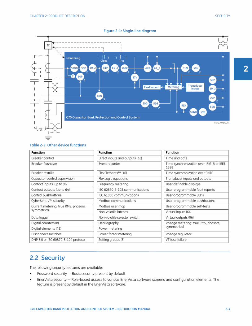
The following single-line diagram illustrates the relay functionality using American National Standards Institute (ANSI) device numbers.
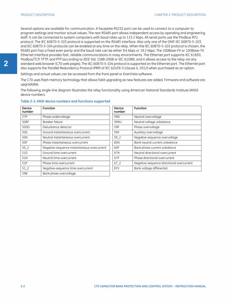
Table 2-1: ANSI device numbers and functions supported
Device number
Function Device number
Function
27P Phase undervoltage 59N Neutral overvoltage
50BF Breaker failure 59NU Neutral voltage unbalance
50DD Disturbance detector 59P Phase overvoltage
50G Ground instantaneous overcurrent 59X Auxiliary overvoltage
50N Neutral instantaneous overcurrent 59_2 Negative-sequence overvoltage
50P Phase instantaneous overcurrent 60N Bank neutral current unbalance
50_2 Negative-sequence instantaneous overcurrent 60P Bank phase current unbalance
51G Ground time overcurrent 67N Neutral directional overcurrent
51N Neutral time overcurrent 67P Phase directional overcurrent
51P Phase time overcurrent 67_2 Negative-sequence directional overcurrent
51_2 Negative-sequence time overcurrent 87V Bank voltage differential
59B Bank phase overvoltage
CHAPTER 2: PRODUCT DESCRIPTION SECURITY
C70 CAPACITOR BANK PROTECTION AND CONTROL SYSTEM – INSTRUCTION MANUAL 2-3
2
Figure 2-1: Single-line diagram
Table 2-2: Other device functions
2.2 SecurityThe following security features are available:
• Password security — Basic security present by default
• EnerVista security — Role-based access to various EnerVista software screens and configuration elements. The feature is present by default in the EnerVista software.
Function Function Function
Breaker control Direct inputs and outputs (32) Time and date
Breaker flashover Event recorder Time synchronization over IRIG-B or IEEE 1588
Breaker restrike FlexElements™ (16) Time synchronization over SNTP
Capacitor control supervision FlexLogic equations Transducer inputs and outputs
Contact inputs (up to 96) Frequency metering User-definable displays
Contact outputs (up to 64) IEC 60870-5-103 communications User-programmable fault reports
Control pushbuttons IEC 61850 communications User-programmable LEDs
CyberSentry™ security Modbus communications User-programmable pushbuttons
Current metering: true RMS, phasors, symmetrical
Modbus user map User-programmable self-tests
Non-volatile latches Virtual inputs (64)
Data logger Non-volatile selector switch Virtual outputs (96)
Digital counters (8) Oscillography Voltage metering: true RMS, phasors, symmetricalDigital elements (48) Power metering
Disconnect switches Power factor metering Voltage regulator
DNP 3.0 or IEC 60870-5-104 protocol Setting groups (6) VT fuse failure

2-4 C70 CAPACITOR BANK PROTECTION AND CONTROL SYSTEM – INSTRUCTION MANUAL
SECURITY CHAPTER 2: PRODUCT DESCRIPTION
2
• CyberSentry security — Advanced security available as a software option. When purchased, the options are automatically enabled, and the default Password security and EnerVista security are disabled.
2.2.0.1 EnerVista securityThe EnerVista security management system is a role-based access control (RBAC) system that allows an administrator to manage the privileges of multiple users. This allows for access control of UR devices by multiple personnel within a substation and conforms to the principles of RBAC as defined in ANSI INCITS 359-2004. The EnerVista security management system is disabled by default to allow the administrator direct access to the EnerVista software after installation. It is recommended that security be enabled before placing the device in service.
Basic password or enhanced CyberSentry security applies, depending on purchase.
2.2.0.2 Password securityPassword security is a basic security feature present by default.
Two levels of password security are provided: command and setting. Use of a password for each level controls whether users can enter commands and/or change settings.
The C70 supports password entry from a local or remote connection. Local access is defined as any access to settings or commands via the faceplate interface. This includes both keypad entry and the through the faceplate RS232 port. Remote access is defined as any access to settings or commands via any rear communications port. This includes both Ethernet and RS485 connections. Any changes to the local or remote passwords enables this functionality.
When entering a settings or command password via EnerVista or any serial interface, the user must enter the corresponding connection password. If the connection is to the back of the C70, the remote password must be used. If the connection is to the RS232 port of the faceplate, the local password applies.
Password access events are logged in the Event Recorder.
2.2.0.3 CyberSentry securityCyberSentry embedded security is a software option that provides advanced security services. When this option is purchased, the basic password security is disabled automatically.
CyberSentry provides security through the following features:
• An Authentication, Authorization, Accounting (AAA) Remote Authentication Dial-In User Service (RADIUS) client that is centrally managed, enables user attribution, provides accounting of all user activities, and uses secure standards-based strong cryptography for authentication and credential protection
• A Role-Based Access Control (RBAC) system that provides a permission model that allows access to UR device operations and configurations based on specific roles and individual user accounts configured on the AAA server (that is, Administrator, Supervisor, Engineer, Operator, Observer roles)
• Security event reporting through the Syslog protocol for supporting Security Information Event Management (SIEM) systems for centralized cybersecurity monitoring
• Strong encryption of all access and configuration network messages between the EnerVista software and UR devices using the Secure Shell (SSH) protocol, the Advanced Encryption Standard (AES), and 128-bit keys in Galois Counter Mode (GCM) as specified in the U.S. National Security Agency Suite B extension for SSH and approved by the National Institute of Standards and Technology (NIST) FIPS-140-2 standards for cryptographic systems
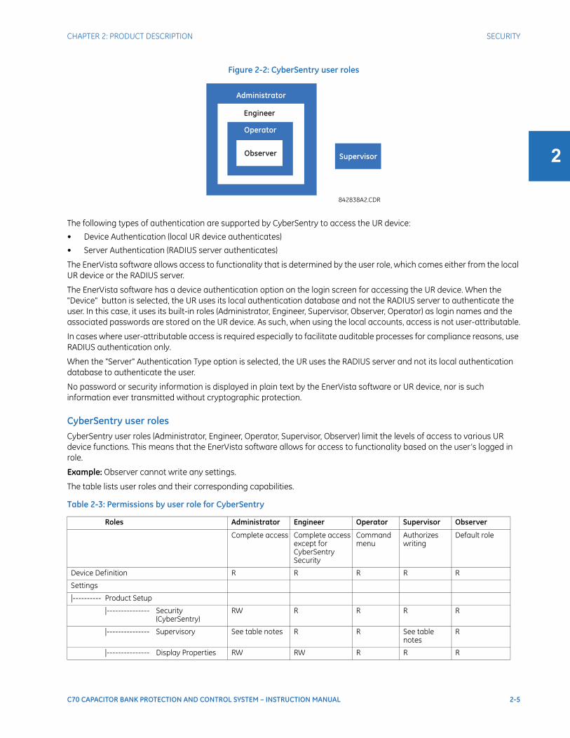
Example: Administrative functions can be segmented away from common operator functions, or engineering type access, all of which are defined by separate roles (see figure) so that access of UR devices by multiple personnel within a substation is allowed. Permissions for each role are outlined in the next section.
CHAPTER 2: PRODUCT DESCRIPTION SECURITY
C70 CAPACITOR BANK PROTECTION AND CONTROL SYSTEM – INSTRUCTION MANUAL 2-5
2
Figure 2-2: CyberSentry user roles
The following types of authentication are supported by CyberSentry to access the UR device:
• Device Authentication (local UR device authenticates)
• Server Authentication (RADIUS server authenticates)
The EnerVista software allows access to functionality that is determined by the user role, which comes either from the local UR device or the RADIUS server.
The EnerVista software has a device authentication option on the login screen for accessing the UR device. When the "Device" button is selected, the UR uses its local authentication database and not the RADIUS server to authenticate the user. In this case, it uses its built-in roles (Administrator, Engineer, Supervisor, Observer, Operator) as login names and the associated passwords are stored on the UR device. As such, when using the local accounts, access is not user-attributable.
In cases where user-attributable access is required especially to facilitate auditable processes for compliance reasons, use RADIUS authentication only.
When the "Server" Authentication Type option is selected, the UR uses the RADIUS server and not its local authentication database to authenticate the user.
No password or security information is displayed in plain text by the EnerVista software or UR device, nor is such information ever transmitted without cryptographic protection.
CyberSentry user rolesCyberSentry user roles (Administrator, Engineer, Operator, Supervisor, Observer) limit the levels of access to various UR device functions. This means that the EnerVista software allows for access to functionality based on the user’s logged in role.
Example: Observer cannot write any settings.
The table lists user roles and their corresponding capabilities.
Table 2-3: Permissions by user role for CyberSentry
Roles Administrator Engineer Operator Supervisor Observer
Complete access Complete access except forCyberSentry Security
Command menu
Authorizeswriting
Default role
Device Definition R R R R R
Settings
|---------- Product Setup
|--------------- Security (CyberSentry)
RW R R R R
|--------------- Supervisory See table notes R R See table notes
R
|--------------- Display Properties RW RW R R R

2-6 C70 CAPACITOR BANK PROTECTION AND CONTROL SYSTEM – INSTRUCTION MANUAL
SECURITY CHAPTER 2: PRODUCT DESCRIPTION
2
|--------------- Clear Relay Records (settings)
RW RW R R R
|--------------- Communications RW RW R R R
|--------------- Modbus User Map RW RW R R R
|--------------- Real Time Clock RW RW R R R
|--------------- Oscillography RW RW R R R
|--------------- Data Logger RW RW R R R
|--------------- Demand RW RW R R R
|--------------- User-Programmable LEDs
RW RW R R R
|--------------- User-Programmable Self Tests
RW RW R R R
|--------------- Control Pushbuttons RW RW R R R
|--------------- User-Programmable Pushbuttons
RW RW R R R
|--------------- Flex state Parameters
RW RW R R R
|--------------- User-Definable Displays
RW RW R R R
|--------------- Direct I/O RW RW R R R
|--------------- Teleprotection RW RW R R R
|--------------- Installation RW RW R R R
|---------- System Setup RW RW R R R
|---------- FlexLogic RW RW R R R
|---------- Grouped Elements RW RW R R R
|---------- Control Elements RW RW R R R
|---------- Inputs / Outputs RW RW R R R
|--------------- Contact Inputs RW RW R R R
|--------------- Contact Input threshold
RW RW R R R
|--------------- Virtual Inputs RW RW R R R
|--------------- Contact Outputs RW RW R R R
|--------------- Virtual Outputs RW RW R R R
|--------------- Resetting RW RW R R R
|--------------- Direct Inputs RW RW R R R
|--------------- Direct Outputs RW RW R R R
|--------------- Teleprotection RW RW R R R
|--------------- Direct Analogs RW RW R R R
|--------------- Direct Integers RW RW R R R
|---------- Transducer I/O RW RW R R R
|---------- Testing RW RW R R R
|---------- Front Panel Labels Designer NA NA NA NA NA
|---------- Protection Summary NA NA NA NA NA
Commands RW RW RW R R
|---------- Virtual Inputs RW RW RW R R
|---------- Clear Records RW RW RW R R
|---------- Set Date and Time RW RW RW R R
User Displays R R R R R
Targets R R R R R
Roles Administrator Engineer Operator Supervisor Observer

CHAPTER 2: PRODUCT DESCRIPTION ORDER CODES
C70 CAPACITOR BANK PROTECTION AND CONTROL SYSTEM – INSTRUCTION MANUAL 2-7
2
Table Notes:
RW = read and write access
R = read access
Supervisor = RW (default), Administrator = R (default), Administrator = RW (only if Supervisor role is disabled)
NA = the permission is not enforced by CyberSentry security
CyberSentry server authenticationThe UR has been designed to direct automatically the authentication requests based on user names. In this respect, local account names on the UR are considered as reserved and not used on a RADIUS server.
The UR detects automatically whether an authentication request is to be handled remotely or locally. As there are five local accounts possible on the UR, if the user ID credential does not match one of the five local accounts, the UR forwards automatically the request to a RADIUS server when one is provided.
If a RADIUS server is provided, but is unreachable over the network, server authentication requests are denied. In this situation, use local UR accounts to gain access to the UR system.
2.3 Order codesThe order code is on the product label and indicates the product options applicable.
The C70 is available as a 19-inch rack horizontal mount or reduced-size (¾) vertical unit and consists of the following modules: power supply, CPU, CT/VT, contact input and output, transducer input and output, and inter-relay communications. Module options are specified at the time of ordering.
Order codes are subject to change without notice. See the ordering page athttp://www.gedigitalenergy.com/multilin/order.htm for the latest options.
The order code depends on the mounting option (horizontal or vertical) and the type of CT/VT modules (enhanced diagnostic CT/VT modules or HardFiberTM process bus modules). The HardFiber process bus module provides an interface to HardFiber Bricks.
Actual Values R R R R R
|---------- Front panel labels designer R R R R R
|---------- Status R R R R R
|---------- Metering R R R R R
|---------- Transducer I/O R R R R R
|---------- Records R R R R R
|---------- Product Info R R R R R
Maintenance RW RW R R R
|---------- Modbus analyzer NA NA NA NA NA
|---------- Change front panel RW RW RW R R
|---------- Update firmware Yes No No No No
|---------- Retrieve file Yes No No No No
Roles Administrator Engineer Operator Supervisor Observer

2-8 C70 CAPACITOR BANK PROTECTION AND CONTROL SYSTEM – INSTRUCTION MANUAL
ORDER CODES CHAPTER 2: PRODUCT DESCRIPTION
2
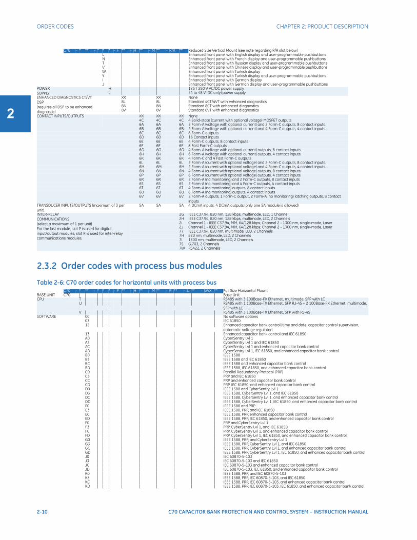
2.3.1 Order codes with enhanced CT/VT modules
Table 2-4: C70 order codes for horizontal unitsC70 - * ** - * * * - F ** - H ** - M ** - P ** - U ** - W/X ** Full Size Horizontal Mount
BASE UNIT C70 | | | | | | | | | | | Base UnitCPU T | | | | | | | | | | RS485 with 3 100Base-FX Ethernet, multimode, SFP with LC
U | | | | | | | | | | RS485 with 1 100Base-TX Ethernet, SFP RJ-45 + 2 100Base-FX Ethernet, multimode, SFP with LC
V | | | | | | | | | | RS485 with 3 100Base-TX Ethernet, SFP with RJ-45SOFTWARE 00 | | | | | | | | | No software options
03 | | | | | | | | | IEC 6185012 | | | | | | | | | Enhanced capacitor bank control (time and date, capacitor control supervision,
automatic voltage regulator)13 | | | | | | | | | Enhanced capacitor bank control and IEC 61850A0 | | | | | | | | | CyberSentry Lvl 1A3 | | | | | | | | | CyberSentry Lvl 1 and IEC 61850AC | | | | | | | | | CyberSentry Lvl 1 and enhanced capacitor bank controlAD | | | | | | | | | CyberSentry Lvl 1, IEC 61850, and enhanced capacitor bank controlB0 | | | | | | | | | IEEE 1588B3 | | | | | | | | | IEEE 1588 and IEC 61850BC | | | | | | | | | IEEE 1588 and enhanced capacitor bank controlBD | | | | | | | | | IEEE 1588, IEC 61850, and enhanced capacitor bank controlC0 | | | | | | | | | Parallel Redundancy Protocol (PRP)C3 | | | | | | | | | PRP and IEC 61850CC | | | | | | | | | PRP and Enhanced Capacitor Bank ControlCD | | | | | | | | | PRP, IEC 61850, and Enhanced Capacitor Bank ControlD0 | | | | | | | | | IEEE 1588 and CyberSentry Lvl 1D3 | | | | | | | | | IEEE 1588, CyberSentry Lvl 1, and IEC 61850DC | | | | | | | | | IEEE 1588, CyberSentry Lvl 1, and enhanced capacitor bank controlDD | | | | | | | | | IEEE 1588, CyberSentry Lvl 1, IEC 61850, and enhanced capacitor bank controlE0 | | | | | | | | | IEEE 1588 and PRPE3 | | | | | | | | | IEEE 1588, PRP, and IEC 61850EC | | | | | | | | | IEEE 1588, PRP, enhanced capacitor bank controlED | | | | | | | | | IEEE 1588, PRP, IEC 61850, and enhanced capacitor bank controlF0 | | | | | | | | | PRP and CyberSentry Lvl 1F3 | | | | | | | | | PRP, CyberSentry Lvl 1, and IEC 61850FC | | | | | | | | | PRP, CyberSentry Lvl 1, and enhanced capacitor bank controlFD | | | | | | | | | PRP, CyberSentry Lvl 1, IEC 61850, and enhanced capacitor bank controlG0 | | | | | | | | | IEEE 1588, PRP, and CyberSentry Lvl 1G3 | | | | | | | | | IEEE 1588, PRP, CyberSentry Lvl 1, and IEC 61850GC | | | | | | | | | IEEE 1588, PRP, CyberSentry Lvl 1, and enhanced capacitor bank controlGD | | | | | | | | | IEEE 1588, PRP, CyberSentry Lvl 1, IEC 61850, and enhanced capacitor bank controlJ0 | | | | | | | | | IEC 60870-5-103J3 | | | | | | | | | IEC 60870-5-103 and IEC 61850JC | | | | | | | | | IEC 60870-5-103 and enhanced capacitor bank controlJD | | | | | | | | | IEC 60870-5-103, IEC 61850, and enhanced capacitor bank controlK0 | | | | | | | | | IEEE 1588, PRP, and IEC 60870-5-103K3 | | | | | | | | | IEEE 1588, PRP, IEC 60870-5-103, and IEC 61850KC | | | | | | | | | IEEE 1588, PRP, IEC 60870-5-103, and enhanced capacitor bank controlKD | | | | | | | | | IEEE 1588, PRP, IEC 60870-5-103, IEC 61850, and enhanced capacitor bank controlL0 | | | | | | | | | IEC 60870-5-103, IEEE 1588, PRP, and CyberSentry Lvl 1L3 | | | | | | | | | IEC 60870-5-103, IEEE 1588, PRP, CyberSentry Lvl 1, and IEC 61850LC | | | | | | | | | IEC 60870-5-103, IEEE 1588, PRP, CyberSentry Lvl 1, and enhanced capacitor bank
controlLD | | | | | | | | | IEC 60870-5-103, IEEE 1588, PRP, CyberSentry Lvl 1, IEC 61850, and enhanced
capacitor bank controlMOUNT/COATING
H | | | | | | | | Horizontal (19” rack)A | | | | | | | | Horizontal (19” rack) with harsh-environment coating
FACEPLATE/ DISPLAY C | | | | | | | English displayP | | | | | | | English display with 4 small and 12 large programmable pushbuttonsD | | | | | | | French displayR | | | | | | | Russian displayA | | | | | | | Chinese displayK | | | | | | | Enhanced front panel with English displayM | | | | | | | Enhanced front panel with French displayQ | | | | | | | Enhanced front panel with Russian displayU | | | | | | | Enhanced front panel with Chinese displayL | | | | | | | Enhanced front panel with English display and user-programmable pushbuttonsN | | | | | | | Enhanced front panel with French display and user-programmable pushbuttonsT | | | | | | | Enhanced front panel with Russian display and user-programmable pushbuttonsV | | | | | | | Enhanced front panel with Chinese display and user-programmable pushbuttonsW | | | | | | | Enhanced front panel with Turkish display Y | | | | | | | Enhanced front panel with Turkish display and user-programmable pushbuttonsI | | | | | | | Enhanced front panel with German display J | | | | | | | Enhanced front panel with German display and user-programmable pushbuttons
CHAPTER 2: PRODUCT DESCRIPTION ORDER CODES
C70 CAPACITOR BANK PROTECTION AND CONTROL SYSTEM – INSTRUCTION MANUAL 2-9
2
Table 2-5: C70 order codes for reduced-size vertical units
POWER SUPPLY
H | | | | | | 125 / 250 V AC/DC power supplyL | | | | | | 24 to 48 V (DC only) power supply
ENHANCED DIAGNOSTICS CT/VT DSP(requires all DSP to be enhanced diagnostic)
| | XX | XX | None8L | 8L | 8L | Standard 4CT/4VT with enhanced diagnostics8N | 8N | 8N | Standard 8CT with enhanced diagnostics8V | 8V | 8V | Standard 8VT with enhanced diagnostics
CONTACT INPUTS/OUTPUTS
XX XX XX XX XX None4C 4C 4C 4C 4C 4 Solid-state (current with optional voltage) MOSFET outputs6A 6A 6A 6A 6A 2 Form-A (voltage with optional current) and 2 Form-C outputs, 8 contact inputs6B 6B 6B 6B 6B 2 Form-A (voltage with optional current) and 4 Form-C outputs, 4 contact inputs6C 6C 6C 6C 6C 8 Form-C outputs6D 6D 6D 6D 6D 16 Contact inputs6E 6E 6E 6E 6E 4 Form-C outputs, 8 contact inputs6F 6F 6F 6F 6F 8 Fast Form-C outputs6G 6G 6G 6G 6G 4 Form-A (voltage with optional current) outputs, 8 contact inputs6H 6H 6H 6H 6H 6 Form-A (voltage with optional current) outputs, 4 contact inputs6K 6K 6K 6K 6K 4 Form-C and 4 Fast Form-C outputs6L 6L 6L 6L 6L 2 Form-A (current with optional voltage) and 2 Form-C outputs, 8 contact inputs6M 6M 6M 6M 6M 2 Form-A (current with optional voltage) and 4 Form-C outputs, 4 contact inputs6N 6N 6N 6N 6N 4 Form-A (current with optional voltage) outputs, 8 contact inputs6P 6P 6P 6P 6P 6 Form-A (current with optional voltage) outputs, 4 contact inputs6R 6R 6R 6R 6R 2 Form-A (no monitoring) and 2 Form-C outputs, 8 contact inputs6S 6S 6S 6S 6S 2 Form-A (no monitoring) and 4 Form-C outputs, 4 contact inputs6T 6T 6T 6T 6T 4 Form-A (no monitoring) outputs, 8 contact inputs6U 6U 6U 6U 6U 6 Form-A (no monitoring) outputs, 4 contact inputs6V 6V 6V 6V 6V 2 Form-A outputs, 1 Form-C output, 2 Form-A (no monitoring) latching outputs, 8
contact inputsTRANSDUCER INPUTS/OUTPUTS (maximum of 3 per unit) 5A 5A 5A 5A 5A 4 DCmA inputs, 4 DCmA outputs (only one 5A module is allowed)INTER-RELAYCOMMUNICATIONS(select a maximum of 1 per unit)
2G IEEE C37.94, 820 nm, 128 kbps, multimode, LED, 1 Channel2H IEEE C37.94, 820 nm, 128 kbps, multimode, LED, 2 Channels2I Channel 1 - IEEE C37.94, MM, 64/128 kbps; Channel 2 - 1300 nm, single-mode, Laser2J Channel 1 - IEEE C37.94, MM, 64/128 kbps; Channel 2 - 1550 nm, single-mode, Laser77 IEEE C37.94, 820 nm, multimode, LED, 2 Channels7H 820 nm, multi-mode, LED, 2 Channels7I 1300 nm, multi-mode, LED, 2 Channels7S G.703, 2 Channels7W RS422, 2 Channels
C70 - * ** - * * * - F ** - H ** - M ** - P/R ** Reduced Size Vertical Mount (see note regarding P/R slot below)BASE UNIT C70 | | | | | | | | | Base UnitCPU T | | | | | | | | RS485 with 3 100Base-FX Ethernet, multimode, SFP with LC
U | | | | | | | | RS485 with 1 100Base-TX Ethernet, SFP RJ-45 + 2 100Base-FX Ethernet, multimode, SFP with LC
V | | | | | | | | RS485 with 3 100Base-TX Ethernet, SFP with RJ-45SOFTWARE 00 | | | | | | | No software options
03 | | | | | | | IEC 6185012 | | | | | | | Enhanced capacitor bank control (time and date, capacitor control supervision, automatic
voltage regulator)13 | | | | | | | Enhanced capacitor bank control and IEC 61850A0 | | | | | | | CyberSentry Lvl 1A3 | | | | | | | CyberSentry Lvl 1 and IEC 61850AC | | | | | | | CyberSentry Lvl 1 and enhanced capacitor bank controlAD | | | | | | | CyberSentry Lvl 1, IEC 61850, and enhanced capacitor bank controlB0 | | | | | | | IEEE 1588B3 | | | | | | | IEEE 1588 and IEC 61850BC | | | | | | | IEEE 1588 and enhanced capacitor bank controlBD | | | | | | | IEEE 1588, IEC 61850, and enhanced capacitor bank controlC0 | | | | | | | Parallel Redundancy Protocol (PRP)C3 | | | | | | | PRP and IEC 61850CC | | | | | | | PRP and enhanced capacitor bank controlCD | | | | | | | PRP, IEC 61850, and enhanced capacitor bank controlD0 | | | | | | | IEEE 1588 and CyberSentry Lvl 1D3 | | | | | | | IEEE 1588, CyberSentry Lvl 1, and IEC 61850DC | | | | | | | IEEE 1588, CyberSentry Lvl 1, and enhanced capacitor bank controlDD | | | | | | | IEEE 1588, CyberSentry Lvl 1, IEC 61850, and enhanced capacitor bank controlE0 | | | | | | | IEEE 1588 and PRPE3 | | | | | | | IEEE 1588, PRP, and IEC 61850EC | | | | | | | IEEE 1588, PRP, enhanced capacitor bank controlED | | | | | | | IEEE 1588, PRP, IEC 61850, and enhanced capacitor bank controlF0 | | | | | | | PRP and CyberSentry Lvl 1F3 | | | | | | | PRP, CyberSentry Lvl 1, and IEC 61850FC | | | | | | | PRP, CyberSentry Lvl 1, and enhanced capacitor bank controlFD | | | | | | | PRP, CyberSentry Lvl 1, IEC 61850, and enhanced capacitor bank controlG0 | | | | | | | IEEE 1588, PRP, and CyberSentry Lvl 1G3 | | | | | | | IEEE 1588, PRP, CyberSentry Lvl 1, and IEC 61850GC | | | | | | | IEEE 1588, PRP, CyberSentry Lvl 1, and enhanced capacitor bank controlGD | | | | | | | IEEE 1588, PRP, CyberSentry Lvl 1, IEC 61850, and enhanced capacitor bank controlJ0 | | | | | | | IEC 60870-5-103J3 | | | | | | | IEC 60870-5-103 and IEC 61850JC | | | | | | | IEC 60870-5-103 and enhanced capacitor bank controlJD | | | | | | | IEC 60870-5-103, IEC 61850, and enhanced capacitor bank controlK0 | | | | | | | IEEE 1588, PRP, and IEC 60870-5-103K3 | | | | | | | IEEE 1588, PRP, IEC 60870-5-103, and IEC 61850KC | | | | | | | IEEE 1588, PRP, IEC 60870-5-103, and enhanced capacitor bank controlKD | | | | | | | IEEE 1588, PRP, IEC 60870-5-103, IEC 61850, and enhanced capacitor bank controlL0 | | | | | | | IEC 60870-5-103, IEEE 1588, PRP, and CyberSentry Lvl 1L3 | | | | | | | IEC 60870-5-103, IEEE 1588, PRP, CyberSentry Lvl 1, and IEC 61850LC | | | | | | | IEC 60870-5-103, IEEE 1588, PRP, CyberSentry Lvl 1, and enhanced capacitor bank controlLD | | | | | | | IEC 60870-5-103, IEEE 1588, PRP, CyberSentry Lvl 1, IEC 61850, and enhanced capacitor bank
controlMOUNT/COATING
V | | | | | | Vertical (3/4 rack)B | | | | | | Vertical (3/4 rack) with harsh-environment coating
FACEPLATE/ DISPLAY F | | | | | English displayD | | | | | French displayR | | | | | Russian displayA | | | | | Chinese displayK | | | | | Enhanced front panel with English displayM | | | | | Enhanced front panel with French displayQ | | | | | Enhanced front panel with Russian displayU | | | | | Enhanced front panel with Chinese display
C70 - * ** - * * * - F ** - H ** - M ** - P ** - U ** - W/X ** Full Size Horizontal Mount
2-10 C70 CAPACITOR BANK PROTECTION AND CONTROL SYSTEM – INSTRUCTION MANUAL
ORDER CODES CHAPTER 2: PRODUCT DESCRIPTION
2
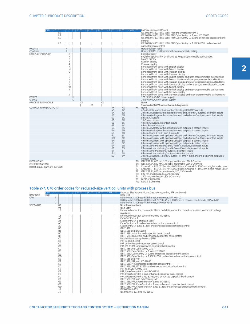
2.3.2 Order codes with process bus modules
Table 2-6: C70 order codes for horizontal units with process bus
L | | | | | Enhanced front panel with English display and user-programmable pushbuttonsN | | | | | Enhanced front panel with French display and user-programmable pushbuttonsT | | | | | Enhanced front panel with Russian display and user-programmable pushbuttonsV | | | | | Enhanced front panel with Chinese display and user-programmable pushbuttonsW | | | | | Enhanced front panel with Turkish displayY | | | | | Enhanced front panel with Turkish display and user-programmable pushbuttonsI | | | | | Enhanced front panel with German displayJ | | | | | Enhanced front panel with German display and user-programmable pushbuttons
POWER SUPPLY
H | | | | 125 / 250 V AC/DC power supplyL | | | | 24 to 48 V (DC only) power supply
ENHANCED DIAGNOSTICS CT/VT DSP(requires all DSP to be enhanced diagnostic)
XX | XX | None8L | 8L | Standard 4CT/4VT with enhanced diagnostics8N | 8N | Standard 8CT with enhanced diagnostics8V | 8V | Standard 8VT with enhanced diagnostics
CONTACT INPUTS/OUTPUTS XX XX XX None4C 4C 4C 4 Solid-state (current with optional voltage) MOSFET outputs6A 6A 6A 2 Form-A (voltage with optional current) and 2 Form-C outputs, 8 contact inputs6B 6B 6B 2 Form-A (voltage with optional current) and 4 Form-C outputs, 4 contact inputs6C 6C 6C 8 Form-C outputs6D 6D 6D 16 Contact inputs6E 6E 6E 4 Form-C outputs, 8 contact inputs6F 6F 6F 8 Fast Form-C outputs6G 6G 6G 4 Form-A (voltage with optional current) outputs, 8 contact inputs6H 6H 6H 6 Form-A (voltage with optional current) outputs, 4 contact inputs6K 6K 6K 4 Form-C and 4 Fast Form-C outputs6L 6L 6L 2 Form-A (current with optional voltage) and 2 Form-C outputs, 8 contact inputs6M 6M 6M 2 Form-A (current with optional voltage) and 4 Form-C outputs, 4 contact inputs6N 6N 6N 4 Form-A (current with optional voltage) outputs, 8 contact inputs6P 6P 6P 6 Form-A (current with optional voltage) outputs, 4 contact inputs6R 6R 6R 2 Form-A (no monitoring) and 2 Form-C outputs, 8 contact inputs6S 6S 6S 2 Form-A (no monitoring) and 4 Form-C outputs, 4 contact inputs6T 6T 6T 4 Form-A (no monitoring) outputs, 8 contact inputs6U 6U 6U 6 Form-A (no monitoring) outputs, 4 contact inputs6V 6V 6V 2 Form-A outputs, 1 Form-C output, 2 Form-A (no monitoring) latching outputs, 8 contact
inputsTRANSDUCER INPUTS/OUTPUTS (maximum of 3 per unit)
5A 5A 5A 4 DCmA inputs, 4 DCmA outputs (only one 5A module is allowed)
INTER-RELAYCOMMUNICATIONS(select a maximum of 1 per unit)For the last module, slot P is used for digital input/output modules; slot R is used for inter-relaycommunications modules.
2G IEEE C37.94, 820 nm, 128 kbps, multimode, LED, 1 Channel2H IEEE C37.94, 820 nm, 128 kbps, multimode, LED, 2 Channels2i Channel 1 - IEEE C37.94, MM, 64/128 kbps; Channel 2 - 1300 nm, single-mode, Laser2J Channel 1 - IEEE C37.94, MM, 64/128 kbps; Channel 2 - 1300 nm, single-mode, Laser77 IEEE C37.94, 820 nm, multimode, LED, 2 Channels7H 820 nm, multimode, LED, 2 Channels7I 1300 nm, multimode, LED, 2 Channels7S G.703, 2 Channels7W RS422, 2 Channels
C70 - * ** - * * * - F ** - H ** - M ** - P ** - U ** - W/X ** Full Size Horizontal MountBASE UNIT C70 | | | | | | | | | | | Base UnitCPU T | | | | | | | | | | RS485 with 3 100Base-FX Ethernet, multimode, SFP with LC
U | | | | | | | | | | RS485 with 1 100Base-TX Ethernet, SFP RJ-45 + 2 100Base-FX Ethernet, multimode, SFP with LC
V | | | | | | | | | | RS485 with 3 100Base-TX Ethernet, SFP with RJ-45SOFTWARE 00 | | | | | | | | | No software options
03 | | | | | | | | | IEC 6185012 | | | | | | | | | Enhanced capacitor bank control (time and date, capacitor control supervision,
automatic voltage regulator)13 | | | | | | | | | Enhanced capacitor bank control and IEC 61850A0 | | | | | | | | | CyberSentry Lvl 1A3 | | | | | | | | | CyberSentry Lvl 1 and IEC 61850AC | | | | | | | | | CyberSentry Lvl 1 and enhanced capacitor bank controlAD | | | | | | | | | CyberSentry Lvl 1, IEC 61850, and enhanced capacitor bank controlB0 | | | | | | | | | IEEE 1588B3 | | | | | | | | | IEEE 1588 and IEC 61850BC | | | | | | | | | IEEE 1588 and enhanced capacitor bank controlBD | | | | | | | | | IEEE 1588, IEC 61850, and enhanced capacitor bank controlC0 | | | | | | | | | Parallel Redundancy Protocol (PRP)C3 | | | | | | | | | PRP and IEC 61850CC | | | | | | | | | PRP and enhanced capacitor bank controlCD | | | | | | | | | PRP, IEC 61850, and enhanced capacitor bank controlD0 | | | | | | | | | IEEE 1588 and CyberSentry Lvl 1D3 | | | | | | | | | IEEE 1588, CyberSentry Lvl 1, and IEC 61850DC | | | | | | | | | IEEE 1588, CyberSentry Lvl 1, and enhanced capacitor bank controlDD | | | | | | | | | IEEE 1588, CyberSentry Lvl 1, IEC 61850, and enhanced capacitor bank controlE0 | | | | | | | | | IEEE 1588 and PRPE3 | | | | | | | | | IEEE 1588, PRP, and IEC 61850EC | | | | | | | | | IEEE 1588, PRP, enhanced capacitor bank controlED | | | | | | | | | IEEE 1588, PRP, IEC 61850, and enhanced capacitor bank controlF0 | | | | | | | | | PRP and CyberSentry Lvl 1F3 | | | | | | | | | PRP, CyberSentry Lvl 1, and IEC 61850FC | | | | | | | | | PRP, CyberSentry Lvl 1, and enhanced capacitor bank controlFD | | | | | | | | | PRP, CyberSentry Lvl 1, IEC 61850, and enhanced capacitor bank controlG0 | | | | | | | | | IEEE 1588, PRP, and CyberSentry Lvl 1G3 | | | | | | | | | IEEE 1588, PRP, CyberSentry Lvl 1, and IEC 61850GC | | | | | | | | | IEEE 1588, PRP, CyberSentry Lvl 1, and enhanced capacitor bank controlGD | | | | | | | | | IEEE 1588, PRP, CyberSentry Lvl 1, IEC 61850, and enhanced capacitor bank controlJ0 | | | | | | | | | IEC 60870-5-103J3 | | | | | | | | | IEC 60870-5-103 and IEC 61850JC | | | | | | | | | IEC 60870-5-103 and enhanced capacitor bank controlJD | | | | | | | | | IEC 60870-5-103, IEC 61850, and enhanced capacitor bank controlK0 | | | | | | | | | IEEE 1588, PRP, and IEC 60870-5-103K3 | | | | | | | | | IEEE 1588, PRP, IEC 60870-5-103, and IEC 61850KC | | | | | | | | | IEEE 1588, PRP, IEC 60870-5-103, and enhanced capacitor bank controlKD | | | | | | | | | IEEE 1588, PRP, IEC 60870-5-103, IEC 61850, and enhanced capacitor bank control
C70 - * ** - * * * - F ** - H ** - M ** - P/R ** Reduced Size Vertical Mount (see note regarding P/R slot below)
CHAPTER 2: PRODUCT DESCRIPTION ORDER CODES
C70 CAPACITOR BANK PROTECTION AND CONTROL SYSTEM – INSTRUCTION MANUAL 2-11
2
Table 2-7: C70 order codes for reduced-size vertical units with process bus
L0 | | | | | | | | | IEC 60870-5-103, IEEE 1588, PRP, and CyberSentry Lvl 1L3 | | | | | | | | | IEC 60870-5-103, IEEE 1588, PRP, CyberSentry Lvl 1, and IEC 61850LC | | | | | | | | | IEC 60870-5-103, IEEE 1588, PRP, CyberSentry Lvl 1, and enhanced capacitor bank
controlLD | | | | | | | | | IEC 60870-5-103, IEEE 1588, PRP, CyberSentry Lvl 1, IEC 61850, and enhanced
capacitor bank controlMOUNT/COATING
H | | | | | | | | Horizontal (19” rack)A | | | | | | | | Horizontal (19” rack) with harsh environmental coating
FACEPLATE/ DISPLAY C | | | | | | | English displayP | | | | | | | English display with 4 small and 12 large programmable pushbuttonsD | | | | | | | French displayR | | | | | | | Russian displayA | | | | | | | Chinese displayK | | | | | | | Enhanced front panel with English displayM | | | | | | | Enhanced front panel with French displayQ | | | | | | | Enhanced front panel with Russian displayU | | | | | | | Enhanced front panel with Chinese displayL | | | | | | | Enhanced front panel with English display and user-programmable pushbuttonsN | | | | | | | Enhanced front panel with French display and user-programmable pushbuttonsT | | | | | | | Enhanced front panel with Russian display and user-programmable pushbuttonsV | | | | | | | Enhanced front panel with Chinese display and user-programmable pushbuttonsW | | | | | | | Enhanced front panel with Turkish display Y | | | | | | | Enhanced front panel with Turkish display and user-programmable pushbuttonsI | | | | | | | Enhanced front panel with German display J | | | | | | | Enhanced front panel with German display and user-programmable pushbuttons
POWER SUPPLY
H | | | | | | 125 / 250 V AC/DC power supplyL | | | | | | 24 to 48 V (DC only) power supply
PROCESS BUS MODULE XX | XX | | | None| 81 | | | | Standard 4CT/4VT with enhanced diagnostics
CONTACT INPUTS/OUTPUTS XX XX XX None4C 4C | 4 Solid-state (current with optional voltage) MOSFET outputs6A 6A | 2 Form-A (voltage with optional current) and 2 Form-C outputs, 8 contact inputs6B 6B | 2 Form-A (voltage with optional current) and 4 Form-C outputs, 4 contact inputs6C 6C | 8 Form-C outputs6D 6D | 16 Contact inputs6E 6E | 4 Form-C outputs, 8 contact inputs6F 6F | 8 Fast Form-C outputs6G 6G | 4 Form-A (voltage with optional current) outputs, 8 contact inputs6H 6H | 6 Form-A (voltage with optional current) outputs, 4 contact inputs6K 6K | 4 Form-C and 4 Fast Form-C outputs6L 6L | 2 Form-A (current with optional voltage) and 2 Form-C outputs, 8 contact inputs6M 6M | 2 Form-A (current with optional voltage) and 4 Form-C outputs, 4 contact inputs6N 6N | 4 Form-A (current with optional voltage) outputs, 8 contact inputs6P 6P | 6 Form-A (current with optional voltage) outputs, 4 contact inputs6R 6R | 2 Form-A (no monitoring) and 2 Form-C outputs, 8 contact inputs6S 6S | 2 Form-A (no monitoring) and 4 Form-C outputs, 4 contact inputs6T 6T | 4 Form-A (no monitoring) outputs, 8 contact inputs6U 6U | 6 Form-A (no monitoring) outputs, 4 contact inputs6V 6V | 2 Form-A outputs, 1 Form-C output, 2 Form-A (no monitoring) latching outputs, 8
contact inputsINTER-RELAYCOMMUNICATIONS(select a maximum of 1 per unit)
2G IEEE C37.94, 820 nm, 128 kbps, multimode, LED, 1 Channel2H IEEE C37.94, 820 nm, 128 kbps, multimode, LED, 2 Channels2I Channel 1 - IEEE C37.94, MM, 64/128 kbps; Channel 2 - 1300 nm, single-mode, Laser2J Channel 1 - IEEE C37.94, MM, 64/128 kbps; Channel 2 - 1550 nm, single-mode, Laser77 IEEE C37.94, 820 nm, multimode, LED, 2 Channels7H 820 nm, multimode, LED, 2 Channels7I 1300 nm, multimode, LED, 2 Channels7S G.703, 2 Channels7W RS422, 2 Channels
C70 - * ** - * * * - F ** - H ** - M ** - P/R ** Reduced Size Vertical Mount (see note regarding P/R slot below)BASE UNIT C70 | | | | | | | | | Base UnitCPU T | | | | | | | | RS485 with 3 100Base-FX Ethernet, multimode, SFP with LC
U | | | | | | | | RS485 with 1 100Base-TX Ethernet, SFP RJ-45 + 2 100Base-FX Ethernet, multimode, SFP with LCV | | | | | | | | RS485 with 3 100Base-TX Ethernet, SFP with RJ-45
SOFTWARE 00 | | | | | | | No software options03 | | | | | | | IEC 6185012 | | | | | | | Enhanced capacitor bank control (time and date, capacitor control supervision, automatic voltage
regulator)13 | | | | | | | Enhanced capacitor bank control and IEC 61850A0 | | | | | | | CyberSentry Lvl 1A3 | | | | | | | CyberSentry Lvl 1 and IEC 61850AC | | | | | | | CyberSentry Lvl 1 and enhanced capacitor bank controlAD | | | | | | | CyberSentry Lvl 1, IEC 61850, and enhanced capacitor bank controlB0 | | | | | | | IEEE 1588B3 | | | | | | | IEEE 1588 and IEC 61850BC | | | | | | | IEEE 1588 and enhanced capacitor bank controlBD | | | | | | | IEEE 1588, IEC 61850, and enhanced capacitor bank controlC0 | | | | | | | Parallel Redundancy Protocol (PRP)C3 | | | | | | | PRP and IEC 61850CC | | | | | | | PRP and enhanced capacitor bank controlCD | | | | | | | PRP, IEC 61850, and enhanced capacitor bank controlD0 | | | | | | | IEEE 1588 and CyberSentry Lvl 1D3 | | | | | | | IEEE 1588, CyberSentry Lvl 1, and IEC 61850DC | | | | | | | IEEE 1588, CyberSentry Lvl 1, and enhanced capacitor bank controlDD | | | | | | | IEEE 1588, CyberSentry Lvl 1, IEC 61850, and enhanced capacitor bank controlE0 | | | | | | | IEEE 1588 and PRPE3 | | | | | | | IEEE 1588, PRP, and IEC 61850EC | | | | | | | IEEE 1588, PRP, enhanced capacitor bank controlED | | | | | | | IEEE 1588, PRP, IEC 61850, and enhanced capacitor bank controlF0 | | | | | | | PRP and CyberSentry Lvl 1F3 | | | | | | | PRP, CyberSentry Lvl 1, and IEC 61850FC | | | | | | | PRP, CyberSentry Lvl 1, and enhanced capacitor bank controlFD | | | | | | | PRP, CyberSentry Lvl 1, IEC 61850, and enhanced capacitor bank controlG0 | | | | | | | IEEE 1588, PRP, and CyberSentry Lvl 1G3 | | | | | | | IEEE 1588, PRP, CyberSentry Lvl 1, and IEC 61850GC | | | | | | | IEEE 1588, PRP, CyberSentry Lvl 1, and enhanced capacitor bank controlGD | | | | | | | IEEE 1588, PRP, CyberSentry Lvl 1, IEC 61850, and enhanced capacitor bank controlJ0 | | | | | | | IEC 60870-5-103J3 | | | | | | | IEC 60870-5-103 and IEC 61850
C70 - * ** - * * * - F ** - H ** - M ** - P ** - U ** - W/X ** Full Size Horizontal Mount

2-12 C70 CAPACITOR BANK PROTECTION AND CONTROL SYSTEM – INSTRUCTION MANUAL
ORDER CODES CHAPTER 2: PRODUCT DESCRIPTION
2
2.3.3 Replacement modulesReplacement modules can be ordered separately. When ordering a replacement CPU module or faceplate, provide the serial number of your existing unit.
Not all replacement modules apply to the C70 relay. The modules specified in the order codes for the C70 are available as replacement modules for the C70.
The order codes shown here are subject to change without notice. See the ordering page at http://www.gedigitalenergy.com/multilin/order.htm for the latest options.
JC | | | | | | | IEC 60870-5-103 and enhanced capacitor bank controlJD | | | | | | | IEC 60870-5-103, IEC 61850, and enhanced capacitor bank controlK0 | | | | | | | IEEE 1588, PRP, and IEC 60870-5-103K3 | | | | | | | IEEE 1588, PRP, IEC 60870-5-103, and IEC 61850KC | | | | | | | IEEE 1588, PRP, IEC 60870-5-103, and enhanced capacitor bank controlKD | | | | | | | IEEE 1588, PRP, IEC 60870-5-103, IEC 61850, and enhanced capacitor bank controlL0 | | | | | | | IEC 60870-5-103, IEEE 1588, PRP, and CyberSentry Lvl 1L3 | | | | | | | IEC 60870-5-103, IEEE 1588, PRP, CyberSentry Lvl 1, and IEC 61850LC | | | | | | | IEC 60870-5-103, IEEE 1588, PRP, CyberSentry Lvl 1, and enhanced capacitor bank controlLD | | | | | | | IEC 60870-5-103, IEEE 1588, PRP, CyberSentry Lvl 1, IEC 61850, and enhanced capacitor bank control
MOUNT/COATING
V | | | | | | Vertical (3/4 rack)B | | | | | | Vertical (3/4 rack) with harsh environmental coating
FACEPLATE/ DISPLAY F | | | | | English displayD | | | | | French displayR | | | | | Russian displayA | | | | | Chinese displayK | | | | | Enhanced front panel with English displayM | | | | | Enhanced front panel with French displayQ | | | | | Enhanced front panel with Russian displayU | | | | | Enhanced front panel with Chinese displayL | | | | | Enhanced front panel with English display and user-programmable pushbuttonsN | | | | | Enhanced front panel with French display and user-programmable pushbuttonsT | | | | | Enhanced front panel with Russian display and user-programmable pushbuttonsV | | | | | Enhanced front panel with Chinese display and user-programmable pushbuttonsW | | | | | Enhanced front panel with Turkish display Y | | | | | Enhanced front panel with Turkish display and user-programmable pushbuttonsI | | | | | Enhanced front panel with German display J | | | | | Enhanced front panel with German display and user-programmable pushbuttons
POWER SUPPLY
H | | | | 125 / 250 V AC/DC power supplyL | | | | 24 to 48 V (DC only) power supply
PROCESS BUS MODULE XX | XX | None| 81 | | Standard 4CT/4VT with enhanced diagnostics
CONTACT INPUTS/OUTPUTS XX None| 4 Solid-state (current with optional voltage) MOSFET outputs| 2 Form-A (voltage with optional current) and 2 Form-C outputs, 8 contact inputs| 2 Form-A (voltage with optional current) and 4 Form-C outputs, 4 contact inputs| 8 Form-C outputs| 16 Contact inputs| 4 Form-C outputs, 8 contact inputs| 8 Fast Form-C outputs| 4 Form-A (voltage with optional current) outputs, 8 contact inputs| 6 Form-A (voltage with optional current) outputs, 4 contact inputs| 4 Form-C and 4 Fast Form-C outputs| 2 Form-A (current with optional voltage) and 2 Form-C outputs, 8 contact inputs| 2 Form-A (current with optional voltage) and 4 Form-C outputs, 4 contact inputs| 4 Form-A (current with optional voltage) outputs, 8 contact inputs| 6 Form-A (current with optional voltage) outputs, 4 contact inputs| 2 Form-A (no monitoring) and 2 Form-C outputs, 8 contact inputs| 2 Form-A (no monitoring) and 4 Form-C outputs, 4 contact inputs| 4 Form-A (no monitoring) outputs, 8 contact inputs| 6 Form-A (no monitoring) outputs, 4 contact inputs| 2 Form-A outputs, 1 Form-C output, 2 Form-A (no monitoring) latching outputs, 8 contact inputs
INTER-RELAYCOMMUNICATIONS(select a maximum of 1 per unit)For the last module, slot P is used for digital and transducerinput/output modules; slot R is used for inter-relaycommunications modules.
2G IEEE C37.94, 820 nm, 128 kbps, multimode, LED, 1 Channel2H IEEE C37.94, 820 nm, 128 kbps, multimode, LED, 2 Channels2I Channel 1 - IEEE C37.94, MM, 64/128 kbps; Channel 2 - 1300 nm, single-mode, Laser2J Channel 1 - IEEE C37.94, MM, 64/128 kbps; Channel 2 - 1550 nm, single-mode, Laser77 IEEE C37.94, 820 nm, multimode, LED, 2 Channels7H 820 nm, multimode, LED, 2 Channels7I 1300 nm, multimode, LED, 2 Channels7S G.703, 2 Channels7W RS422, 2 Channels
C70 - * ** - * * * - F ** - H ** - M ** - P/R ** Reduced Size Vertical Mount (see note regarding P/R slot below)

CHAPTER 2: PRODUCT DESCRIPTION ORDER CODES
C70 CAPACITOR BANK PROTECTION AND CONTROL SYSTEM – INSTRUCTION MANUAL 2-13
2
Table 2-8: UR order codes for replacement modules, horizontal unitsUR - ** - *
POWER SUPPLY (redundant supply only available in horizontal units and must be same type as main supply) (for redundant supply, must swap both power supplies when switching from RH to SH)
| SH A | 125 / 300 V AC/DC| RL H | 24 to 48 V (DC only)
CPU | T | RS485 with 3 100Base-FX Ethernet, multimode, SFP with LC| U | RS485 with 1 100Base-TX Ethernet, SFP RJ-45 + 2 100Base-FX Ethernet, multimode, SFP with LC| V | RS485 with 3 100Base-TX Ethernet, SFP with RJ-45
FACEPLATE/DISPLAY | 3C | Horizontal faceplate with keypad and English display| 3D | Horizontal faceplate with keypad and French display| 3R | Horizontal faceplate with keypad and Russian display| 3A | Horizontal faceplate with keypad and Chinese display| 3P | Horizontal faceplate with keypad, user-programmable pushbuttons, and English display| 3G | Horizontal faceplate with keypad, user-programmable pushbuttons, and French display| 3S | Horizontal faceplate with keypad, user-programmable pushbuttons, and Russian display| 3B | Horizontal faceplate with keypad, user-programmable pushbuttons, and Chinese display| 3K | Enhanced front panel with English display| 3M | Enhanced front panel with French display| 3Q | Enhanced front panel with Russian display| 3U | Enhanced front panel with Chinese display| 3L | Enhanced front panel with English display and user-programmable pushbuttons| 3N | Enhanced front panel with French display and user-programmable pushbuttons| 3T | Enhanced front panel with Russian display and user-programmable pushbuttons| 3V | Enhanced front panel with Chinese display and user-programmable pushbuttons| 3I | Enhanced front panel with German display| 3J | Enhanced front panel with German display and user-programmable pushbuttons
CONTACT INPUTS AND OUTPUTS | 4A | 4 Solid-State (no monitoring) MOSFET outputs| 4B | 4 Solid-State (voltage with optional current) MOSFET outputs| 4C | 4 Solid-State (current with optional voltage) MOSFET outputs| 4D | 16 Contact inputs with Auto-Burnishing| 4L | 14 Form-A (no monitoring) Latching outputs| 67 | 8 Form-A (no monitoring) outputs| 6A | 2 Form-A (voltage with optional current) and 2 Form-C outputs, 8 contact inputs| 6B | 2 Form-A (voltage with optional current) and 4 Form-C outputs, 4 contact inputs| 6C | 8 Form-C outputs| 6D | 16 Contact inputs| 6E | 4 Form-C outputs, 8 contact inputs| 6F | 8 Fast Form-C outputs| 6G | 4 Form-A (voltage with optional current) outputs, 8 contact inputs| 6H | 6 Form-A (voltage with optional current) outputs, 4 contact inputs| 6K | 4 Form-C and 4 Fast Form-C outputs| 6L | 2 Form-A (current with optional voltage) and 2 Form-C outputs, 8 contact inputs| 6M | 2 Form-A (current with optional voltage) and 4 Form-C outputs, 4 contact inputs| 6N | 4 Form-A (current with optional voltage) outputs, 8 contact inputs| 6P | 6 Form-A (current with optional voltage) outputs, 4 contact inputs| 6R | 2 Form-A (no monitoring) and 2 Form-C outputs, 8 contact inputs| 6S | 2 Form-A (no monitoring) and 4 Form-C outputs, 4 contact inputs| 6T | 4 Form-A (no monitoring) outputs, 8 contact inputs| 6U | 6 Form-A (no monitoring) outputs, 4 contact inputs| 6V | 2 Form-A outputs, 1 Form-C output, 2 Form-A (no monitoring) latching outputs, 8 contact inputs
CT/VT MODULES(not available for the C30)
| 8L | Standard 4CT/4VT with enhanced diagnostics| 8N | Standard 8CT with enhanced diagnostics| 8M | Sensitive Ground 4CT/4VT with enhanced diagnostics| 8R | Sensitive Ground 8CT with enhanced diagnostics
INTER-RELAY COMMUNICATIONS | 2A | C37.94SM, 1300 nm single-mode, ELED, 1 channel single-mode| 2B | C37.94SM, 1300 nm single-mode, ELED, 2 channel single-mode| 2E | Bi-phase, single channel| 2F | Bi-phase, dual channel| 2G | IEEE C37.94, 820 nm, 128 kbps, multimode, LED, 1 Channel| 2H | IEEE C37.94, 820 nm, 128 kbps, multimode, LED, 2 Channels| 2I | Channel 1 - IEEE C37.94, multimode, 64/128 kbps; Channel 2 - 1300 nm, single-mode, Laser| 2J | Channel 1 - IEEE C37.94, multimode, 64/128 kbps; Channel 2 - 1550 nm, single-mode, Laser| 72 | 1550 nm, single-mode, Laser, 1 Channel| 73 | 1550 nm, single-mode, Laser, 2 Channel| 74 | Channel 1 - RS422; Channel 2 - 1550 nm, single-mode, Laser| 75 | Channel 1 - G.703; Channel 2 - 1550 nm, single-mode Laser| 76 | IEEE C37.94, 820 nm, multimode, LED, 1 Channel| 77 | IEEE C37.94, 820 nm, multimode, LED, 2 Channels| 7A | 820 nm, multimode, LED, 1 Channel| 7B | 1300 nm, multimode, LED, 1 Channel| 7C | 1300 nm, single-mode, ELED, 1 Channel| 7D | 1300 nm, single-mode, Laser, 1 Channel| 7E | Channel 1 - G.703; Channel 2 - 820 nm, multimode| 7F | Channel 1 - G.703; Channel 2 - 1300 nm, multimode| 7G | Channel 1 - G.703; Channel 2 - 1300 nm, single-mode ELED| 7H | 820 nm, multimode, LED, 2 Channels| 7I | 1300 nm, multimode, LED, 2 Channels| 7J | 1300 nm, single-mode, ELED, 2 Channels| 7K | 1300 nm, single-mode, Laser, 2 Channels| 7L | Channel 1 - RS422; Channel 2 - 820 nm, multimode, LED| 7M | Channel 1 - RS422; Channel 2 - 1300 nm, multimode, LED| 7N | Channel 1 - RS422; Channel 2 - 1300 nm, single-mode, ELED| 7P | Channel 1 - RS422; Channel 2 - 1300 nm, single-mode, Laser| 7Q | Channel 1 - G.703; Channel 2 - 1300 nm, single-mode Laser| 7R | G.703, 1 Channel| 7S | G.703, 2 Channels| 7T | RS422, 1 Channel| 7W | RS422, 2 Channels
TRANSDUCER INPUTS/OUTPUTS | 5A | 4 DCmA inputs, 4 DCmA outputs (only one 5A module is allowed)| 5C | 8 RTD inputs| 5D | 4 RTD inputs, 4 DCmA outputs (only one 5D module is allowed)| 5E | 4 DCmA inputs, 4 RTD inputs| 5F | 8 DCmA inputs
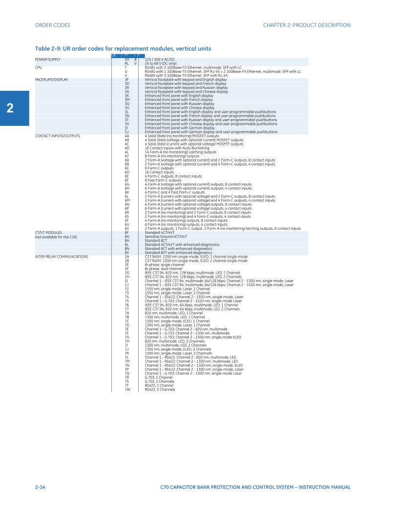
2-14 C70 CAPACITOR BANK PROTECTION AND CONTROL SYSTEM – INSTRUCTION MANUAL
ORDER CODES CHAPTER 2: PRODUCT DESCRIPTION
2
Table 2-9: UR order codes for replacement modules, vertical unitsUR - ** - *
POWER SUPPLY | SH B | 125 / 300 V AC/DC| RL V | 24 to 48 V (DC only)
CPU | T | RS485 with 3 100Base-FX Ethernet, multimode, SFP with LC| U | RS485 with 1 100Base-TX Ethernet, SFP RJ-45 + 2 100Base-FX Ethernet, multimode, SFP with LC| V | RS485 with 3 100Base-TX Ethernet, SFP with RJ-45
FACEPLATE/DISPLAY | 3F | Vertical faceplate with keypad and English display| 3D | Vertical faceplate with keypad and French display| 3R | Vertical faceplate with keypad and Russian display| 3A | Vertical faceplate with keypad and Chinese display| 3K | Enhanced front panel with English display| 3M | Enhanced front panel with French display| 3Q | Enhanced front panel with Russian display| 3U | Enhanced front panel with Chinese display| 3L | Enhanced front panel with English display and user-programmable pushbuttons| 3N | Enhanced front panel with French display and user-programmable pushbuttons| 3T | Enhanced front panel with Russian display and user-programmable pushbuttons| 3V | Enhanced front panel with Chinese display and user-programmable pushbuttons| 3I | Enhanced front panel with German display| 3J | Enhanced front panel with German display and user-programmable pushbuttons
CONTACT INPUTS/OUTPUTS | 4A | 4 Solid-State (no monitoring) MOSFET outputs| 4B | 4 Solid-State (voltage with optional current) MOSFET outputs| 4C | 4 Solid-State (current with optional voltage) MOSFET outputs| 4D | 16 Contact inputs with Auto-Burnishing| 4L | 14 Form-A (no monitoring) Latching outputs| 67 | 8 Form-A (no monitoring) outputs| 6A | 2 Form-A (voltage with optional current) and 2 Form-C outputs, 8 contact inputs| 6B | 2 Form-A (voltage with optional current) and 4 Form-C outputs, 4 contact inputs| 6C | 8 Form-C outputs| 6D | 16 Contact inputs| 6E | 4 Form-C outputs, 8 contact inputs| 6F | 8 Fast Form-C outputs| 6G | 4 Form-A (voltage with optional current) outputs, 8 contact inputs| 6H | 6 Form-A (voltage with optional current) outputs, 4 contact inputs| 6K | 4 Form-C and 4 Fast Form-C outputs| 6L | 2 Form-A (current with optional voltage) and 2 Form-C outputs, 8 contact inputs| 6M | 2 Form-A (current with optional voltage) and 4 Form-C outputs, 4 contact inputs| 6N | 4 Form-A (current with optional voltage) outputs, 8 contact inputs| 6P | 6 Form-A (current with optional voltage) outputs, 4 contact inputs| 6R | 2 Form-A (no monitoring) and 2 Form-C outputs, 8 contact inputs| 6S | 2 Form-A (no monitoring) and 4 Form-C outputs, 4 contact inputs| 6T | 4 Form-A (no monitoring) outputs, 8 contact inputs| 6U | 6 Form-A (no monitoring) outputs, 4 contact inputs| 6V | 2 Form-A outputs, 1 Form-C output, 2 Form-A (no monitoring) latching outputs, 8 contact inputs
CT/VT MODULES(not available for the C30)
| 8F | Standard 4CT/4VT| 8G | Sensitive Ground 4CT/4VT| 8H | Standard 8CT| 8L | Standard 4CT/4VT with enhanced diagnostics| 8N | Standard 8CT with enhanced diagnostics| 8V | Standard 8VT with enhanced diagnostics
INTER-RELAY COMMUNICATIONS | 2A | C37.94SM, 1300 nm single-mode, ELED, 1 channel single-mode| 2B | C37.94SM, 1300 nm single-mode, ELED, 2 channel single-mode| 2E | Bi-phase, single channel| 2F | Bi-phase, dual channel| 2G | IEEE C37.94, 820 nm, 128 kbps, multimode, LED, 1 Channel| 2H | IEEE C37.94, 820 nm, 128 kbps, multimode, LED, 2 Channels| 2I | Channel 1 - IEEE C37.94, multimode, 64/128 kbps; Channel 2 - 1300 nm, single-mode, Laser| 2J | Channel 1 - IEEE C37.94, multimode, 64/128 kbps; Channel 2 - 1550 nm, single-mode, Laser| 72 | 1550 nm, single-mode, Laser, 1 Channel| 73 | 1550 nm, single-mode, Laser, 2 Channel| 74 | Channel 1 - RS422; Channel 2 - 1550 nm, single-mode, Laser| 75 | Channel 1 - G.703; Channel 2 - 1550 nm, single-mode Laser| 76 | IEEE C37.94, 820 nm, 64 kbps, multimode, LED, 1 Channel| 77 | IEEE C37.94, 820 nm, 64 kbps, multimode, LED, 2 Channels| 7A | 820 nm, multimode, LED, 1 Channel| 7B | 1300 nm, multimode, LED, 1 Channel| 7C | 1300 nm, single-mode, ELED, 1 Channel| 7D | 1300 nm, single-mode, Laser, 1 Channel| 7E | Channel 1 - G.703; Channel 2 - 820 nm, multimode| 7F | Channel 1 - G.703; Channel 2 - 1300 nm, multimode| 7G | Channel 1 - G.703; Channel 2 - 1300 nm, single-mode ELED| 7H | 820 nm, multimode, LED, 2 Channels| 7I | 1300 nm, multimode, LED, 2 Channels| 7J | 1300 nm, single-mode, ELED, 2 Channels| 7K | 1300 nm, single-mode, Laser, 2 Channels| 7L | Channel 1 - RS422; Channel 2 - 820 nm, multimode, LED| 7M | Channel 1 - RS422; Channel 2 - 1300 nm, multimode, LED| 7N | Channel 1 - RS422; Channel 2 - 1300 nm, single-mode, ELED| 7P | Channel 1 - RS422; Channel 2 - 1300 nm, single-mode, Laser| 7Q | Channel 1 - G.703; Channel 2 - 1300 nm, single-mode Laser| 7R | G.703, 1 Channel| 7S | G.703, 2 Channels| 7T | RS422, 1 Channel| 7W | RS422, 2 Channels
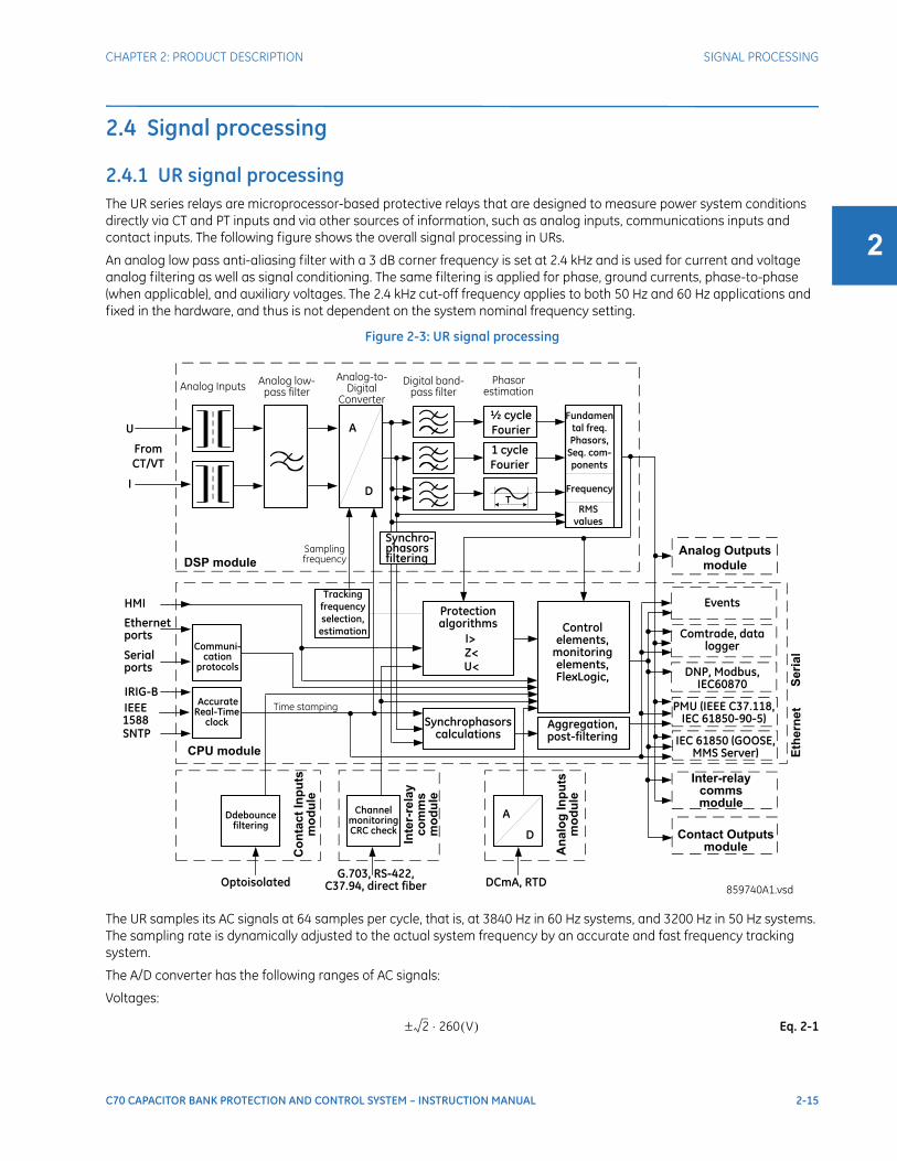
CHAPTER 2: PRODUCT DESCRIPTION SIGNAL PROCESSING
C70 CAPACITOR BANK PROTECTION AND CONTROL SYSTEM – INSTRUCTION MANUAL 2-15
2
2.4 Signal processing
2.4.1 UR signal processingThe UR series relays are microprocessor-based protective relays that are designed to measure power system conditions directly via CT and PT inputs and via other sources of information, such as analog inputs, communications inputs and contact inputs. The following figure shows the overall signal processing in URs.
An analog low pass anti-aliasing filter with a 3 dB corner frequency is set at 2.4 kHz and is used for current and voltage analog filtering as well as signal conditioning. The same filtering is applied for phase, ground currents, phase-to-phase (when applicable), and auxiliary voltages. The 2.4 kHz cut-off frequency applies to both 50 Hz and 60 Hz applications and fixed in the hardware, and thus is not dependent on the system nominal frequency setting.
Figure 2-3: UR signal processing
The UR samples its AC signals at 64 samples per cycle, that is, at 3840 Hz in 60 Hz systems, and 3200 Hz in 50 Hz systems. The sampling rate is dynamically adjusted to the actual system frequency by an accurate and fast frequency tracking system.
The A/D converter has the following ranges of AC signals:
Voltages:
Eq. 2-1
From CT/VT
U
I
Analog Inputs Analog low-pass filter
Analog-to-Digital
Converter
A
Digital band-pass filter
DSP module
Phasor estimation
½ cycle Fourier
1 cycle Fourier
RMS values
Fundamental freq. Phasors,
Seq. com-ponents
D
Sampling frequency
CPU module
I>Z<U<
Protection algorithms
IRIG-BIEEE 1588SNTP
Tracking frequency selection,
estimation
Accurate Real-Time
clock Synchrophasors calculations
Serial ports
Ethernet ports
Communi-cation
protocols
Control elements,
monitoring elements, FlexLogic,
Aggregation, post-filtering
Con
tact
Inpu
ts
mod
ule
HMI
Ddebounce filtering
Optoisolated
Ana
log
Inpu
ts
mod
ule
DCmA, RTD
A
DInte
r-re
lay
com
ms
mod
ule
Channel monitoring CRC check
G.703, RS-422, C37.94, direct fiber
Contact Outputs module
Ethe
rnet
Seria
l
PMU (IEEE C37.118,IEC 61850-90-5)
IEC 61850 (GOOSE, MMS Server)
DNP, Modbus, IEC60870
Comtrade, data logger
Events
Inter-relaycomms module
FrequencyT
Analog Outputs module
Time stamping
Synchro-phasors filtering
859740A1.vsd
2± 260 V( )⋅
2-16 C70 CAPACITOR BANK PROTECTION AND CONTROL SYSTEM – INSTRUCTION MANUAL
SIGNAL PROCESSING CHAPTER 2: PRODUCT DESCRIPTION
2
Currents:
Eq. 2-2
Current harmonics are estimated based on raw samples with the use of the full-cycle Fourier filter. Harmonics 2nd through 25th are estimated.
True RMS value for the current is calculated on a per-phase basis. The true RMS can be used for demand recording or as an input signal to Time Overcurrent function, if the latter is intended for thermal protection. The true RMS is calculated as per the widely accepted definition:
Eq. 2-3
RMS values include harmonics, inter-harmonics, DC components, and so on, along with fundamental frequency values. The true RMS value reflects thermal effects of the current and is used for the thermal related monitoring and protection functions.
Protection and control functions respond to phasors of the fundamental and/or harmonic frequency components (magnitudes and angles), with an exception for some functions that have an option for RMS or fundamental measurements, or some function responding to RMS only. This type of response is explained typically in each element's section in the instruction manual.
Currents are pre-filtered using a Finite Impulse Response (FIR) digital filter. The filter is designed to reject DC components and low-frequency distortions, without amplifying high-frequency noise. This filter is referred to as a modified MIMIC filter, which provides excellent filtering and overall balance between speed and accuracy of filtering. The filter is cascaded with the full-cycle Fourier filter for the current phasor estimation.
Voltages are pre-filtered using a patented Finite Impulse Response (FIR) digital filter. The filter has been optimized to reject voltage transformers specific distortions, such as Capacitive Voltage Transformer (CVT) noise and high-frequency oscillatory components. The filter is cascaded with the half-cycle Fourier filter for the voltage phasor estimation.
The URs measure power system frequency using the Clarke transformation by estimating the period of the waveform from two consecutive zero-crossings in the same direction (negative-to-positive). Voltage or current samples are pre-filtered using a Finite Impulse Response (FIR) digital filter to remove high frequency noise contained in the signal. The period is used after several security conditions are met, such as true RMS signal must be above 6% nominal for a certain time and others. If these security conditions are not met, the last valid measurement is used for a specific time after which the UR reverts to nominal system frequency.
Synchrophasors are calculated using a patented convolution integral algorithm. This algorithm allows use of the same time stamped samples, which are used for protection and taken at the same sampling frequency. This allows URs to use one sampling clock for both protection algorithms and synchrophasors.
Synchrophasors on firmware versions 7.23 and up have been tested and certified to meet IEEE C.37.118-2011 and C.37.118.1a-2014 standards for both metering and protection classes with outputs available up to 60 synchrophasors per second for the metering class and 120 synchrophasors per second for the protection class. Synchrophasors measurement are also available via IEC 61850-90-5 protocol.
Contact inputs threshold is settable in the firmware with 17, 33, 84, 166 VDC settings available. Inputs are scanned every 0.5 ms and can be conditioned for the critical applications, using debounce time timer, settable from 0.0 ms to 16.0 ms. Contact inputs with auto-burnishing are available as well, when external contacts are exposed to the contamination in a harsh industrial environment.
All measured values are available in the UR metering section on the front panel and via communications protocols. Measured analog values and binary signals can be captured in COMTRADE format with sampling rates from 8 to 64 samples per power cycle. Analog values can be captured with Data Logger, allowing much slower rates extended over long period of time.
Other advanced UR order code options are available to support IEC 61850 Ed2.0 (including fast GOOSE, MMS server, 61850 services, ICD/CID/IID files, and so on), IEEE 1588 (IEEE C37.238 power profile) based time synchronization, CyberSentry (advanced cyber security), the Parallel Redundancy Protocol (PRP), IEC 60870-5-103, and so on.
2± 46rated A( )⋅
IRMS t( )1T-- i2 t( ) td
t T–( )
t
=
CHAPTER 2: PRODUCT DESCRIPTION SPECIFICATIONS
C70 CAPACITOR BANK PROTECTION AND CONTROL SYSTEM – INSTRUCTION MANUAL 2-17
2
2.5 SpecificationsSpecifications are subject to change without notice.
2.5.1 Protection elementsThe operating times include the activation time of a trip rated form-A output contact unless otherwise indicated. FlexLogic operands of a given element are 4 ms faster. Take this into account when using FlexLogic to interconnect with other protection or control elements of the relay, building FlexLogic equations, or interfacing with other intelligent electronic devices (IEDs) or power system devices via communications or different output contacts. If not specified, the operate times given here are for a 60 Hz system at nominal system frequency. Operate times for a 50 Hz system are 1.2 times longer.
VOLTAGE DIFFERENTIALOperation: per phaseAuto-setting: on demand from keypad, per phaseNumber of elements: 1 per VT bank, maximum of 3Matching factor: 0.5000 to 2000.0000 in steps of 0.0001, per phaseNumber of trip/alarm stages: 4 per phase with individual timers per stagePickup threshold: 0.001 to 1.000 pu of bus voltage in steps of 0.001Pickup level accuracy: 0.003 puHysteresis: 3% or 0.0005 pu, whichever is greater Pickup delay: 0 to 600.00 s in steps of 0.01Timer accuracy: ±3% of operate time or ±35 ms, whichever is greaterOperate time: <35 ms at 60 Hz
CAPACITOR CONTROLFunctionality: contains remote/local and auto/manual non-volatile latches, collects trip, open and close input
requests and issues outputs to control tripping and closingClosing inhibit delay: 0 to 60 minutes in steps of 1 secondTrip and close seal-in timers: 0 to 60.000 s in steps of 0.001
AUTOMATIC VOLTAGE REGULATORNumber of elements: 1 per CT/VT module, maximum of 3Modes: voltage with load drop compensation or reactive power with power factor limitMinimum voltage supervision: 0.500 to 1.500 pu in steps of 0.001Close voltage level: 0.750 to 1.500 pu in steps of 0.001Open voltage level: 0.750 to 1.500 pu in steps of 0.001Voltage pickup accuracy: ±0.5% of setting from 10 to 208 VClose reactive power level: –1.50 to 1.50 pu in steps of 0.01Open reactive power level: –1.50 to 1.50 pu in steps of 0.01Power pickup accuracy: ±0.05 puPower factor limit 0.50 to 1.00 in steps of 0.01Power factor accuracy: ±0.05Hysteresis: 0.02 pu (voltage); 0.05 pu (vars)Close delay: 0 to 65.353 s in steps of 0.001Open delay: 0 to 65.353 s in steps of 0.001Timer accuracy: ±3% of operate time or ±20 ms, whichever is greaterOperate time: <80 ms at 60 Hz
PHASE/NEUTRAL/GROUND TOCCurrent: Phasor or RMSPickup level: 0.000 to 30.000 pu in steps of 0.001Dropout level: 97% to 98% of pickupLevel accuracy:
0.1 to 2.0 × CT: ±0.5% of reading or ±0.4% of rated (whichever is greater)> 2.0 × CT: ±1.5% of reading > 2.0 × CT rating

2-18 C70 CAPACITOR BANK PROTECTION AND CONTROL SYSTEM – INSTRUCTION MANUAL
SPECIFICATIONS CHAPTER 2: PRODUCT DESCRIPTION
2
Curve shapes: IEEE Moderately/Very/Extremely Inverse; IEC (and BS) A/B/C and Short Inverse; GE IAC Inverse, Short/Very/ Extremely Inverse; I2t; FlexCurves™ (programmable); Definite Time (0.01 s base curve)
Curve multiplier: Time Dial = 0.00 to 600.00 in steps of 0.01Reset type: Instantaneous/Timed (per IEEE)Curve timing accuracy at 1.03 to 20 x pickup:
±3.5% of operate time or ±½ cycle (whichever is greater) from pickup to operateVoltage restraint: Modifies pickup current for voltage in the range of 0.1 < V < 0.9 VT Nominal in a fixed linear rela-
tionship
PHASE/NEUTRAL/GROUND IOCPickup level: 0.000 to 30.000 pu in steps of 0.001Dropout level: 97 to 98% of pickupLevel accuracy:
0.1 to 2.0 × CT rating: ±0.5% of reading or ±0.4% of rated (whichever is greater)> 2.0 × CT rating: ±1.5% of reading
Overreach: <2%Pickup delay: 0.00 to 600.00 s in steps of 0.01Reset delay: 0.00 to 600.00 s in steps of 0.01Operate time: <16 ms at 3 × pickup at 60 Hz (Phase/Ground IOC)
<20 ms at 3 × pickup at 60 Hz (Neutral IOC)Timer accuracy: ±3% of operate time or ±1/4 cycle (whichever is greater)
NEGATIVE SEQUENCE TOCPickup level: 0.000 to 30.000 pu in steps of 0.001Dropout level: 97% to 98% of pickupLevel accuracy: ±0.5% of reading or ±0.4% of rated (whichever is greater)
from 0.1 to 2.0 x CT rating±1.5% of reading > 2.0 x CT rating
Curve shapes: IEEE Moderately/Very/Extremely Inverse; IEC (and BS) A/B/C and Short Inverse; GE IAC Inverse, Short/Very/ Extremely Inverse; I2t; FlexCurves™ (programmable); Definite Time (0.01 s base curve)
Curve multiplier (Time dial): 0.00 to 600.00 in steps of 0.01Reset type: Instantaneous/Timed (per IEEE) and LinearCurve timing accuracyat 1.03 to 20 x pickup: ±3.5% of operate time or ±½ cycle (whichever is greater) from pickup to operate
NEGATIVE SEQUENCE IOCPickup level: 0.000 to 30.000 pu in steps of 0.001Dropout level: 97 to 98% of pickupLevel accuracy: 0.1 to 2.0 × CT rating: ±0.5% of reading or ±0.4% of rated (whichever is greater); >2.0 × CT rating:
±1.5% of readingOverreach: <2%Pickup delay: 0.00 to 600.00 s in steps of 0.01Reset delay: 0.00 to 600.00 s in steps of 0.01Operate time: <20 ms at 3 × pickup at 60 HzTimer accuracy: ±3% of operate time or ±1/4 cycle (whichever is greater)
PHASE DIRECTIONAL OVERCURRENTRelay connection: 90° (quadrature)Quadrature voltage: ABC phase seq.: phase A (VBC), phase B (VCA), phase C (VAB); ACB phase seq.: phase A (VCB), phase
B (VAC), phase C (VBA)Polarizing voltage threshold: 0.000 to 3.000 pu in steps of 0.001Current sensitivity threshold: 0.05 puCharacteristic angle: 0 to 359° in steps of 1Angle accuracy: ±2°Operation time (FlexLogic operands):
Tripping (reverse load, forward fault): <12 ms, typically

CHAPTER 2: PRODUCT DESCRIPTION SPECIFICATIONS
C70 CAPACITOR BANK PROTECTION AND CONTROL SYSTEM – INSTRUCTION MANUAL 2-19
2
Blocking (forward load, reverse fault): <8 ms, typically
NEUTRAL DIRECTIONAL OVERCURRENTDirectionality: Co-existing forward and reversePolarizing: Voltage, Current, Dual, Dual-V, Dual-IPolarizing voltage: V_0 or VXPolarizing current: IGOperating current: I_0Level sensing: 3 × (|I_0| – K × |I_1|), IG
Independent for forward and reverseRestraint, K: 0.000 to 0.500 in steps of 0.001Characteristic angle: –90 to 90° in steps of 1Limit angle: 40 to 90° in steps of 1, independent for forward and reverseAngle accuracy: ±2°Offset impedance: 0.00 to 250.00 Ω in steps of 0.01Pickup level: 0.002 to 30.000 pu in steps of 0.01Dropout level: 97 to 98%Operation time: <16 ms at 3 × pickup at 60 Hz
NEGATIVE SEQUENCE DIRECTIONAL OCDirectionality: Co-existing forward and reversePolarizing: VoltagePolarizing voltage: V_2Operating current: I_2Level sensing:
Zero-sequence: |I_0| – K × |I_1|Negative-sequence: |I_2| – K × |I_1|
Restraint, K: 0.000 to 0.500 in steps of 0.001Characteristic angle: 0 to 90° in steps of 1Limit angle: 40 to 90° in steps of 1, independent for forward and reverseAngle accuracy: ±2°Offset impedance: 0.00 to 250.00 Ω in steps of 0.01Pickup level: 0.015 to 30.000 pu in steps of 0.01Dropout level: 97 to 98%Operation time: <16 ms at 3 × pickup at 60 Hz
PHASE CURRENT UNBALANCEOperation: per phaseAuto-setting: on demand from keypad, per phaseNumber of elements: 1 per CT bank, maximum of 3Inherent unbalance factor: –0.1000 to 0.1000 in steps of 0.0001, per phaseNumber of trip/alarm stages: 4 per phase with individual timers per stagePickup threshold: 0.001 to 5.000 pu of split-phase CT nominal in steps of 0.001Pickup level accuracy: 0.002 pu for <1 pu current and <20 CT mismatch between phase and differential CTHysteresis: 3% or 0.001 pu, whichever is greaterPickup delay: 0 to 600.00 s in steps of 0.01Timer accuracy: ±3% of operate time or ±35 ms, whichever is greaterOperate time: <35 ms at 60 Hz
NEUTRAL CURRENT UNBALANCEAuto-setting: on demand from keypadNumber of elements: 1 per CT bank, to a maximum of 3Inherent unbalance factor: magnitude of 0 to 0.1500 in steps of 0.0001, angle of 0 to 359° in steps of 1Number of trip/alarm stages: 4, with individual timers per stagePickup threshold: 0.001 to 5.000 pu of ground input CT in steps of 0.001Pickup level accuracy: 0.002 pu for <1 pu current and < 20 CT mismatch between phase and neutral CTHysteresis: 3% or 0.001 pu, whichever is greater
2-20 C70 CAPACITOR BANK PROTECTION AND CONTROL SYSTEM – INSTRUCTION MANUAL
SPECIFICATIONS CHAPTER 2: PRODUCT DESCRIPTION
2
Slope: 0.0 to 10.0% in steps of 0.1Pickup delay: 0 to 600.00 s in steps of 0.01Timer accuracy: ±3% of operate time or ±35 ms, whichever is greaterOperate time: <35 ms at 60 Hz
NEUTRAL VOLTAGE UNBALANCEOperation: compensated for inherent bank and system unbalanceAuto-setting: on demand from keypadNumber of elements: 1 per VT bank, maximum of 3Compensating factor: 0.7500 to 1.2500 in steps of 0.0001Number of trip/alarm stages: 4 with individual timersPickup threshold: 0.001 to 1.000 pu of nominal of the bank neutral point VT in steps of 0.001Slope: 0 to 10% in steps of 0.1Pickup level accuracy: 0.003 pu for <10 VT mismatch between phase and neutral VTHysteresis: 3% or 0.001 pu whichever is greaterPickup delay: 0 to 600.00 s in steps of 0.01Timer accuracy: ±3% of operate time or ±35 ms, whichever is greaterOperate time: <35 ms at 60 Hz
PHASE UNDERVOLTAGEPickup level: 0.000 to 3.000 pu in steps of 0.001Dropout level: 102 to 103% of pickupLevel accuracy: ±0.5% of reading from 10 to 208 VCurve shapes: GE IAV Inverse;
Definite Time (0.1s base curve)Curve multiplier: Time dial = 0.00 to 600.00 in steps of 0.01Curve timing accuracy at <0.90 x pickup:
±3.5% of operate time or ±1/2 cycle (whichever is greater) from pickup to operate
BANK OVERVOLTAGEOperation: per phase, 3 stages of definite-time, 1 stage of inverse-timeApplication: grounded and ungrounded banksNumber of elements: 1 per VT bank, maximum of 3Pickup threshold: 0.800 to 2.000 pu of bus voltage in steps of 0.001, per phasePickup level accuracy: 0.002 pu for operating voltage <70 VHysteresis: 0.02 puPickup delay: 0 to 600.00 s in steps of 0.01Curve: any user-programmable FlexCurveTimer accuracy: ±3% of operate time or ±35 ms, whichever is greaterOperate time: <35 ms at 60 Hz
PHASE OVERVOLTAGEVoltage: Phasor onlyPickup level: 0.000 to 3.000 pu in steps of 0.001Dropout level: 97 to 98% of pickupLevel accuracy: ±0.5% of reading from 10 to 208 VPickup delay: 0.00 to 600.00 in steps of 0.01 sOperate time: <30 ms at 1.10 × pickup at 60 HzTimer accuracy: ±3% of operate time or ±1/4 cycle (whichever is greater)
NEUTRAL OVERVOLTAGEPickup level: 0.000 to 3.000 pu in steps of 0.001Dropout level: 97 to 98% of pickupLevel accuracy: ±0.5% of reading from 10 to 208 VPickup delay: 0.00 to 600.00 s in steps of 0.01 (definite time) or user-defined curveReset delay: 0.00 to 600.00 s in steps of 0.01Curve timing accuracy at >1.1 pickup: ±3.5% of operate time or ±1 cycle (whichever is greater) from pickup to operateOperate time: <30 ms at 1.10 pickup at 60 Hz

CHAPTER 2: PRODUCT DESCRIPTION SPECIFICATIONS
C70 CAPACITOR BANK PROTECTION AND CONTROL SYSTEM – INSTRUCTION MANUAL 2-21
2
AUXILIARY OVERVOLTAGEPickup level: 0.000 to 3.000 pu in steps of 0.001Dropout level: 97 to 98% of pickupLevel accuracy: ±0.5% of reading from 10 to 208 VPickup delay: 0 to 600.00 s in steps of 0.01Reset delay: 0 to 600.00 s in steps of 0.01Timer accuracy: ±3% of operate time or ±1/4 cycle (whichever is greater)Operate time: <30 ms at 1.10 × pickup at 60 Hz
NEGATIVE SEQUENCE OVERVOLTAGEPickup level: 0.000 to 1.250 pu in steps of 0.001Dropout level: 97 to 98% of pickupLevel accuracy: ±0.5% of reading from 10 to 208 VPickup delay: 0 to 600.00 s in steps of 0.01Reset delay: 0 to 600.00 s in steps of 0.01Timer accuracy: ±3% of operate time or ±20 ms, whichever is greaterOperate time: <30 ms at 1.10 × pickup at 60 Hz
BREAKER FAILUREMode: 1-pole, 3-poleCurrent supervision: phase, neutral currentCurrent supv. pickup: 0.001 to 30.000 pu in steps of 0.001Current supv. dropout: 97 to 98% of pickupCurrent supv. accuracy:
0.1 to 2.0 × CT rating: ±0.75% of reading or ±2% of rated (whichever is greater)above 2 × CT rating: ±2.5% of reading
BREAKER FLASHOVEROperating quantity: phase current, voltage, and voltage differencePickup level voltage: 0 to 1.500 pu in steps of 0.001Dropout level voltage: 97 to 98% of pickupPickup level current: 0 to 1.500 pu in steps of 0.001Dropout level current: 97 to 98% of pickupLevel accuracy: ±0.5% or ±0.1% of rated, whichever is greaterPickup delay: 0 to 65.535 s in steps of 0.001Timer accuracy: ±3% of operate time or ±42 ms, whichever is greaterOperate time: <42 ms at 1.10 × pickup at 60 Hz
BREAKER RESTRIKEPrinciple: detection of high-frequency overcurrent condition ¼ cycle after breaker opensAvailability: one per CT/VT module (not including 8Z modules)Pickup level: 0.1 to 2.00 pu in steps of 0.01Reset delay: 0.000 to 65.535 s in steps of 0.001
THERMAL OVERLOAD PROTECTIONThermal overload curves: IEC 255-8 curveBase current: 0.20 to 3.00 pu in steps of 0.01Overload (k) factor: 1.00 to 1.20 pu in steps of 0.05Trip time constant: 0 to 1000 min. in steps of 1Reset time constant: 0 to 1000 min. in steps of 1Minimum reset time: 0 to 1000 min. in steps of 1Timer accuracy (cold curve): ±100 ms or 2%, whichever is greaterTimer accuracy (hot curve): ±500 ms or 2%, whichever is greater for Ip < 0.9 × k × Ib and I / (k × Ib) > 1.1
TRIP BUS (TRIP WITHOUT FLEXLOGIC)Number of elements: 6Number of inputs: 16Operate time: <2 ms at 60 Hz

2-22 C70 CAPACITOR BANK PROTECTION AND CONTROL SYSTEM – INSTRUCTION MANUAL
SPECIFICATIONS CHAPTER 2: PRODUCT DESCRIPTION
2
Timer accuracy: ±3% or 10 ms, whichever is greater
2.5.2 User-programmable elements
FLEXLOGICProgramming language: Reverse Polish Notation with graphical visualization (keypad programmable)Lines of code: 512Internal variables: 64Supported operations: NOT, XOR, OR (2 to 16 inputs), AND (2 to 16 inputs), NOR (2 to 16 inputs), NAND (2 to 16 inputs),
latch (reset-dominant), edge detectors, timersInputs: any logical variable, contact, or virtual inputNumber of timers: 32Pickup delay: 0 to 60000 (ms, sec., min.) in steps of 1Dropout delay: 0 to 60000 (ms, sec., min.) in steps of 1
FLEXCURVES™Number: 4 (A through D)Reset points: 40 (0 through 1 of pickup)Operate points: 80 (1 through 20 of pickup)Time delay: 0 to 65535 ms in steps of 1
FLEX STATESNumber: up to 256 logical variables grouped under 16 Modbus addressesProgrammability: any logical variable, contact, or virtual input
FLEXELEMENTS™Number of elements: 16Operating signal: any analog actual value, or two values in differential modeOperating signal mode: signed or absolute valueOperating mode: level, deltaComparator direction: over, underPickup Level: –90.000 to 90.000 pu in steps of 0.001Hysteresis: 0.1 to 50.0% in steps of 0.1Delta dt: 20 ms to 60 daysPickup and dropout delay: 0.000 to 65.535 s in steps of 0.001
NON-VOLATILE LATCHESType: set-dominant or reset-dominantNumber: 16 (individually programmed)Output: stored in non-volatile memoryExecution sequence: as input prior to protection, control, and FlexLogic
USER-PROGRAMMABLE LEDsNumber: 48 plus trip and alarmProgrammability: from any logical variable, contact, or virtual inputReset mode: self-reset or latched
LED TESTInitiation: from any contact input or user-programmable conditionNumber of tests: 3, interruptible at any timeDuration of full test: approximately 3 minutesTest sequence 1: all LEDs onTest sequence 2: all LEDs off, one LED at a time on for 1 sTest sequence 3: all LEDs on, one LED at a time off for 1 s
USER-DEFINABLE DISPLAYSNumber of displays: 16

CHAPTER 2: PRODUCT DESCRIPTION SPECIFICATIONS
C70 CAPACITOR BANK PROTECTION AND CONTROL SYSTEM – INSTRUCTION MANUAL 2-23
2
Lines of display: 2 × 20 alphanumeric charactersParameters: up to 5, any Modbus register addressesInvoking and scrolling: keypad, or any user-programmable condition, including pushbuttons
CONTROL PUSHBUTTONSNumber of pushbuttons: 7Operation: drive FlexLogic operands
USER-PROGRAMMABLE PUSHBUTTONS (OPTIONAL)Number of pushbuttons: 12 (standard faceplate);
16 (enhanced faceplate)Mode: self-reset, latchedDisplay message: 2 lines of 20 characters eachDrop-out timer: 0.00 to 60.00 s in steps of 0.05Autoreset timer: 0.2 to 600.0 s in steps of 0.1Hold timer: 0.0 to 10.0 s in steps of 0.1
SELECTOR SWITCHNumber of elements: 2Upper position limit: 1 to 7 in steps of 1Selecting mode: time-out or acknowledgeTime-out timer: 3.0 to 60.0 s in steps of 0.1Control inputs: step-up and 3-bitPower-up mode: restore from non-volatile memory or synchronize to a 3-bit control input or synch/restore mode
TIME OF DAY TIMERSNumber of timers: 5Setting resolution: 1 minute
DIGITAL ELEMENTSNumber of elements: 48Operating signal: any FlexLogic operandPickup delay: 0.000 to 999999.999 s in steps of 0.001Dropout delay: 0.000 to 999999.999 s in steps of 0.001Timing accuracy: ±3% or ±4 ms, whichever is greater
2.5.3 Monitoring
OSCILLOGRAPHYMaximum records: 64Sampling rate: 64 samples per power cycleTriggers: any element pickup, dropout, or operate; contact input change of state; contact output change
of state; FlexLogic equationData: AC input channels; element state; contact input state; contact output stateData storage: in non-volatile memory
EVENT RECORDERCapacity: 1024 eventsTime-tag: to 1 microsecondTriggers: any element pickup, dropout, or operate; contact input change of state; contact output change
of state; self-test eventsData storage: in non-volatile memory
USER-PROGRAMMABLE FAULT REPORTNumber of elements: 2Pre-fault trigger: any FlexLogic operandFault trigger: any FlexLogic operandRecorder quantities: 32 (any FlexAnalogTM value)

2-24 C70 CAPACITOR BANK PROTECTION AND CONTROL SYSTEM – INSTRUCTION MANUAL
SPECIFICATIONS CHAPTER 2: PRODUCT DESCRIPTION
2
DATA LOGGERNumber of channels: 1 to 16Parameters: any available analog actual valueSampling rate: 15 to 3600000 ms in steps of 1Trigger: any FlexLogic operandMode: continuous or triggeredStorage capacity: (NN is dependent on memory)
1-second rate:01 channel for NN days
16 channels for NN days↓
60-minute rate:01 channel for NN days16 channels for NN days
2.5.4 Metering
RMS CURRENT: PHASE, NEUTRAL, AND GROUNDAccuracy at
0.1 to 2.0 × CT rating: ±0.25% of reading or ±0.1% of rated (whichever is greater)> 2.0 × CT rating: ±1.0% of reading
RMS VOLTAGEAccuracy: ±0.5% of reading from 10 to 208 V
REAL POWER (WATTS)Accuracy at 0.1 to 1.5 x CT rating and 0.8 to 1.2 x VT rating:
±1.0% of reading at –1.0 ≤ PF < –0.8 and 0.8 < PF ≤ 10
REACTIVE POWER (VARS)Accuracy at 0.1 to 1.5 x CT rating and 0.8 to 1.2 x VT rating:
±1.0% of reading at –0.2 ≤ PF ≤ 0.2
APPARENT POWER (VA)Accuracy at 0.1 to 1.5 x CT rating and 0.8 to 1.2 x VT rating:
±1.0% of reading
CURRENT HARMONICSHarmonics: 2nd to 25th harmonic: per phase, displayed as a % of f1 (fundamental frequency phasor)
THD: per phase, displayed as a % of f1Accuracy:
HARMONICS: 1. f1 > 0.4pu: (0.20% + 0.035% / harmonic) of reading or 0.15% of 100%, whichever is greater2. f1 < 0.4pu: as above plus %error of f1
THD: 1. f1 > 0.4pu: (0.25% + 0.035% / harmonic) of reading or 0.20% of 100%, whichever is greater2. f1 < 0.4pu: as above plus %error of f1
VOLTAGE HARMONICSHarmonics: 2nd to 25th harmonic: per phase, displayed as a % of f1 (fundamental frequency phasor)
THD: per phase, displayed as a % of f1Accuracy:
HARMONICS: 1. f1 > 0.4pu: (0.20% + 0.035% / harmonic) of reading or 0.15% of 100%, whichever is greater2. f1 < 0.4pu: as above plus %error of f1
THD: 1. f1 > 0.4pu: (0.25% + 0.035% / harmonic) of reading or 0.20% of 100%, whichever is greater2. f1 < 0.4pu: as above plus %error of f1
FREQUENCYAccuracy at
V = 0.8 to 1.2 pu: ±0.01 Hz (when voltage signal is used for frequency measurement)
CHAPTER 2: PRODUCT DESCRIPTION SPECIFICATIONS
C70 CAPACITOR BANK PROTECTION AND CONTROL SYSTEM – INSTRUCTION MANUAL 2-25
2
I = 0.1 to 0.25 pu: ±0.05 HzI > 0.25 pu: ±0.02 Hz (when current signal is used for frequency measurement)
2.5.5 Inputs
AC CURRENTCT rated primary: 1 to 50000 ACT rated secondary: 1 A or 5 A by connectionRelay burden: < 0.2 VA at rated secondaryConversion range:
Standard CT: 0.02 to 46 × CT rating RMS symmetricalCurrent withstand: 20 ms at 250 times rated
1 sec at 100 times ratedcontinuous 4xInom
Short circuit rating: 150000 RMS symmetrical amperes, 250 V maximum (primary current to external CT)
AC VOLTAGEVT rated secondary: 50.0 to 240.0 VVT ratio: 1.00 to 24000.00Relay burden: < 0.25 VA at 120 VConversion range: 1 to 275 VVoltage withstand: continuous at 260 V to neutral
1 min/hr at 420 V to neutral
FREQUENCYNominal frequency setting: 25 to 60 HzSampling frequency: 64 samples per power cycleTracking frequency range: 20 to 70 Hz
CONTACT INPUTSDry contacts: 1000 Ω maximumWet contacts: 300 V DC maximumSelectable thresholds: 17 V, 33 V, 84 V, 166 VTolerance: ±10%Contacts per common return: 4Recognition time: < 1 msDebounce time: 0.0 to 16.0 ms in steps of 0.5Continuous current draw: 4 mA (when energized)
CONTACT INPUTS WITH AUTO-BURNISHINGDry contacts: 1000 Ω maximumWet contacts: 300 V DC maximumSelectable thresholds: 17 V, 33 V, 84 V, 166 VTolerance: ±10%Contacts per common return: 2Recognition time: < 1 msDebounce time: 0.0 to 16.0 ms in steps of 0.5Continuous current draw: 4 mA (when energized)Auto-burnish impulse current: 50 to 70 mADuration of auto-burnish impulse: 25 to 50 ms
DCMA INPUTSCurrent input (mA DC): 0 to –1, 0 to +1, –1 to +1, 0 to 5, 0 to 10, 0 to 20, 4 to 20 (programmable)Input impedance: 379 Ω ±10%Conversion range: –1 to + 20 mA DCAccuracy: ±0.2% of full scaleType: Passive

2-26 C70 CAPACITOR BANK PROTECTION AND CONTROL SYSTEM – INSTRUCTION MANUAL
SPECIFICATIONS CHAPTER 2: PRODUCT DESCRIPTION
2
IRIG-B INPUTAmplitude modulation: 1 to 10 V pk-pkDC shift: TTL–CompatibleInput impedance: 50 kΩIsolation: 2 kV
DIRECT INPUTSInput points: 32Remote devices: 16Default states on loss of comms.: On, Off, Latest/Off, Latest/OnRing configuration: Yes, NoData rate: 64 or 128 kbpsCRC: 32-bitCRC alarm:
Responding to: Rate of messages failing the CRCMonitoring message count: 10 to 10000 in steps of 1Alarm threshold: 1 to 1000 in steps of 1
Unreturned message alarm:Responding to: Rate of unreturned messages in the ring configurationMonitoring message count: 10 to 10000 in steps of 1Alarm threshold: 1 to 1000 in steps of 1
2.5.6 Power supply
LOW RANGENominal DC voltage: 24 to 48 VMinimum DC voltage: 20 VMaximum DC voltage: 60 V for RL power supply module, 75 V for SL power supply moduleVoltage loss hold-up: 200 ms duration at maximum loadNOTE: Low range is DC only.
HIGH RANGENominal DC voltage: 125 to 250 VMinimum DC voltage: 88 VMaximum DC voltage: 300 VNominal AC voltage: 100 to 240 V at 50/60 HzMinimum AC voltage: 88 V at 25 to 100 HzMaximum AC voltage: 265 V at 25 to 100 HzVoltage loss hold-up: 200 ms duration at maximum load
ALL RANGESVolt withstand: 2 × Highest Nominal Voltage for 10 msPower consumption: typical = 15 to 20 W/VA
maximum = 45 W/VAcontact factory for exact order code consumption
INTERNAL FUSERatings:
Low range power supply: 8 A / 250 VHigh range power supply: 4 A / 250 V
Interrupting capacity:AC: 100 000 A RMS symmetricalDC: 10 000 A

CHAPTER 2: PRODUCT DESCRIPTION SPECIFICATIONS
C70 CAPACITOR BANK PROTECTION AND CONTROL SYSTEM – INSTRUCTION MANUAL 2-27
2
2.5.7 Outputs
FORM-A RELAYMake and carry for 0.2 s: 30 A as per ANSI C37.90Carry continuous: 6 ABreak (DC inductive, L/R = 40 ms):
Operate time: < 4 msContact material: silver alloy
LATCHING RELAYMake and carry for 0.2 s: 30 A as per ANSI C37.90Carry continuous: 6 A as per IEEE C37.90Break (DC resistive as per IEC61810-1):
Operate time: < 4 msContact material: silver alloyControl: separate operate and reset inputsControl mode: operate-dominant or reset-dominant
FORM-A VOLTAGE MONITORApplicable voltage: approx. 15 to 250 V DCTrickle current: approx. 1 to 2.5 mA
FORM-A CURRENT MONITORThreshold current: approx. 80 to 100 mA
FORM-C AND CRITICAL FAILURE RELAYMake and carry for 0.2 s: 30 A as per ANSI C37.90Carry continuous: 8 ABreak (DC inductive, L/R = 40 ms):
Operate time: < 8 msContact material: silver alloy
FAST FORM-C RELAYMake and carry: 0.1 A max. (resistive load)
Voltage Current
24 V 1 A
48 V 0.5 A
125 V 0.3 A
250 V 0.2 A
Voltage Current
24 V 6 A
48 V 1.6 A
125 V 0.4 A
250 V 0.2 A
Voltage Current
24 V 1 A
48 V 0.5 A
125 V 0.3 A
250 V 0.2 A

2-28 C70 CAPACITOR BANK PROTECTION AND CONTROL SYSTEM – INSTRUCTION MANUAL
SPECIFICATIONS CHAPTER 2: PRODUCT DESCRIPTION
2
Minimum load impedance:
Operate time: < 0.6 msInternal Limiting Resistor: 100 Ω, 2 W
SOLID-STATE OUTPUT RELAYOperate and release time: <100 μsMaximum voltage: 265 V DCMaximum continuous current: 5 A at 45°C; 4 A at 65°CMake and carry:
for 0.2 s: 30 A as per ANSI C37.90for 0.03 s: 300 A
Breaking capacity:
CONTROL POWER EXTERNAL OUTPUT (FOR DRY CONTACT INPUT)Capacity: 100 mA DC at 48 V DCIsolation: ±300 Vpk
DIRECT OUTPUTSOutput points: 32
DCMA OUTPUTSRange: –1 to 1 mA, 0 to 1 mA, 4 to 20 mAMax. load resistance: 12 kΩ for –1 to 1 mA range
12 kΩ for 0 to 1 mA range600 Ω for 4 to 20 mA range
Accuracy: ±0.75% of full-scale for 0 to 1 mA range±0.5% of full-scale for –1 to 1 mA range±0.75% of full-scale for 0 to 20 mA range
99% Settling time to a step change: 100 msIsolation: 1.5 kVDriving signal: any FlexAnalog quantityUpper and lower limit for the driving signal: –90 to 90 pu in steps of 0.001
Input voltage Impedance
2 W Resistor 1 W Resistor
250 V DC 20 KΩ 50 KΩ120 V DC 5 KΩ 2 KΩ48 V DC 2 KΩ 2 KΩ24 V DC 2 KΩ 2 KΩNote: values for 24 V and 48 V are the same due to a required 95% voltage drop across the load impedance.
UL 508 Utility application(autoreclose scheme)
Industrial application
Operations/interval
5000 ops /1 s-On, 9 s-Off
5 ops /0.2 s-On, 0.2 s-Offwithin 1 minute
10000 ops /0.2 s-On, 30 s-Off
1000 ops /0.5 s-On, 0.5 s-Off
Break capability(0 to 250 V DC)
3.2 AL/R = 10 ms
10 AL/R = 40 ms
10 AL/R = 40 ms
1.6 AL/R = 20 ms
0.8 AL/R = 40 ms

CHAPTER 2: PRODUCT DESCRIPTION SPECIFICATIONS
C70 CAPACITOR BANK PROTECTION AND CONTROL SYSTEM – INSTRUCTION MANUAL 2-29
2
2.5.8 Communications
IEC 61850IEC 61850: Supports IEC 61850 Edition 2.0. See the UR Series Communications Guide and its conformance
statements.
RS232Front port: 19.2 or 115.2 kbps, Modbus RTU
RS4851 rear port: up to 115 kbps, Modbus RTU, DNP 3, IEC 60870-5-103Typical distance: 1200 mIsolation: 2 kV, isolated together at 36 Vpk
ETHERNET (FIBER)
ETHERNET (10/100 MB TWISTED PAIR)Modes: 10 Mb, 10/100 Mb (auto-detect)Connector: RJ45
SIMPLE NETWORK TIME PROTOCOL (SNTP)Clock synchronization error: <10 ms (typical)
PRECISION TIME PROTOCOL (PTP)PTP IEEE Std 1588 2008 (version 2)Power Profile (PP) per IEEE Standard PC37.238TM2011Slave-only ordinary clockPeer delay measurement mechanism
PARALLEL REDUNDANCY PROTOCOL (PRP) (IEC 62439-3 CLAUSE 4, 2012)Ethernet ports used: 2 and 3Networks supported: 10/100 Mb Ethernet
OTHERTFTP, SFTP, HTTP, IEC 60870-5-104, Ethernet Global Data (EGD), IEEE C37.118
Parameter Fiber type
100 Mb multimode
Wavelength 1310 nm
Connector ST
Transmit power –20 dBm
Receiver sensitivity –30 dBm
Power budget 10 dB
Maximum input power
–14 dBm
Typical distance 2 km
Duplex full/half
Redundancy yes
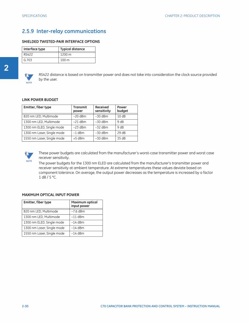
2-30 C70 CAPACITOR BANK PROTECTION AND CONTROL SYSTEM – INSTRUCTION MANUAL
SPECIFICATIONS CHAPTER 2: PRODUCT DESCRIPTION
2
2.5.9 Inter-relay communications
SHIELDED TWISTED-PAIR INTERFACE OPTIONS
LINK POWER BUDGET
MAXIMUM OPTICAL INPUT POWER
Interface type Typical distance
RS422 1200 m
G.703 100 m
NOTE
RS422 distance is based on transmitter power and does not take into consideration the clock source provided by the user.
Emitter, fiber type Transmit power
Received sensitivity
Power budget
820 nm LED, Multimode –20 dBm –30 dBm 10 dB
1300 nm LED, Multimode –21 dBm –30 dBm 9 dB
1300 nm ELED, Single mode –23 dBm –32 dBm 9 dB
1300 nm Laser, Single mode –1 dBm –30 dBm 29 dB
1550 nm Laser, Single mode +5 dBm –30 dBm 35 dB
NOTE
These power budgets are calculated from the manufacturer’s worst-case transmitter power and worst case receiver sensitivity.The power budgets for the 1300 nm ELED are calculated from the manufacturer's transmitter power and receiver sensitivity at ambient temperature. At extreme temperatures these values deviate based on component tolerance. On average, the output power decreases as the temperature is increased by a factor 1 dB / 5 °C.
Emitter, fiber type Maximum optical input power
820 nm LED, Multimode –7.6 dBm
1300 nm LED, Multimode –11 dBm
1300 nm ELED, Single mode –14 dBm
1300 nm Laser, Single mode –14 dBm
1550 nm Laser, Single mode –14 dBm

CHAPTER 2: PRODUCT DESCRIPTION SPECIFICATIONS
C70 CAPACITOR BANK PROTECTION AND CONTROL SYSTEM – INSTRUCTION MANUAL 2-31
2
TYPICAL LINK DISTANCE
Compensated difference in transmitting and receiving (channel asymmetry) channel delays using GPS satellite clock: 10 ms
2.5.10 Environmental
AMBIENT TEMPERATURESStorage temperature: –40 to 85°COperating temperature: –40 to 60°C; the LCD contrast can be impaired at temperatures less than –20°C
HUMIDITYHumidity: operating up to 95% (non-condensing) at 55°C (as per IEC60068-2-30 variant 1, 6 days)
OTHERAltitude: 2000 m (maximum)Pollution degree: IIOvervoltage category: IIIngress protection: IP20 front, IP10 backNoise: 0 dB
Emitter, fiber type Cable type Connector type
Typical distance
820 nm LED,multimode
62.5/125 μm ST 1.65 km
50/125 μm ST 1.65 km
1300 nm LED,multimode
62.5/125 μm ST 4 km
50/125 μm ST 4 km
NOTE
Typical distances listed are based on the following assumptions for system loss. As actual losses vary from one installation to another, the distance covered by your system can vary.
CONNECTOR LOSSES (TOTAL OF BOTH ENDS)ST connector: 2 dB
FIBER LOSSES820 nm multimode: 3 dB/km1300 nm multimode: 1 dB/km1300 nm single mode: 0.35 dB/kmSplice losses: one splice every 2 km at 0.05 dB loss per splice
SYSTEM MARGIN3 dB additional loss added to calculations to compensate for all other losses.

2-32 C70 CAPACITOR BANK PROTECTION AND CONTROL SYSTEM – INSTRUCTION MANUAL
SPECIFICATIONS CHAPTER 2: PRODUCT DESCRIPTION
2
2.5.11 Type tests
C70 TYPE TESTS
1 Not tested by third party.
2.5.12 Production tests
THERMALProducts go through an environmental test based upon an Accepted Quality Level (AQL) sampling process.
Test Reference standard Test level
Dielectric voltage withstand EN 60255-51 2.2 kV
Impulse voltage withstand EN 60255-51 5 kV
Damped oscillatory IEC 61000-4-18 / IEC 60255-22-1 2.5 kV CM, 1 kV DM
Electrostatic discharge EN 61000-4-2 / IEC 60255-22-2 Level 3
RF immunity EN 61000-4-3 / IEC 60255-22-3 Level 3
Fast transient disturbance EN 61000-4-4 / IEC 60255-22-4 Class A and B
Surge immunity EN 61000-4-5 / IEC 60255-22-5 Level 3 and 4
Conducted RF immunity EN 61000-4-6 / IEC 60255-22-6 Level 3
Power frequency immunity EN 61000-4-71 / IEC 60255-22-7 Class A and B
Voltage interruption and ripple DC IEC 60255-11 12% ripple, 200 ms interrupts
Radiated and conducted emissions CISPR11 / CISPR22 / IEC 60255-25 Class A
Sinusoidal vibration IEC 60255-21-1 Class 1
Shock and bump IEC 60255-21-2 Class 1
Seismic IEC 60255-21-3 Class 1
Power magnetic immunity IEC 61000-4-8 Level 5
Pulse magnetic immunity IEC 61000-4-9 Level 4
Damped magnetic immunity IEC 61000-4-10 Level 4
Voltage dip and interruption IEC 61000-4-11 0, 40, 70, 80% dips; 250 / 300 cycle interrupts
Damped oscillatory IEC 61000-4-121 2.5 kV CM, 1 kV DM
Conducted RF immunity, 0 to 150 kHz IEC 61000-4-16 Level 4
Voltage ripple IEC 61000-4-17 15% ripple
Ingress protection IEC 605291 IP40 front, IP10 back
Cold IEC 60068-2-1 –40°C for 16 hours
Hot IEC 60068-2-2 85°C for 16 hours
Humidity IEC 60068-2-30 6 days, variant 1
Damped oscillatory IEEE/ANSI C37.90.1 2.5 kV, 1 MHz
RF immunity IEEE/ANSI C37.90.2 20 V/m, 80 MHz to 1 GHz
Safety UL 5081 e83849 NKCR
Safety UL C22.2-141 e83849 NKCR7
Safety UL 10531 e83849 NKCR
Safety IEC 60255-27 Insulation: class 1, Pollution degree: 2, Over voltage cat II

CHAPTER 2: PRODUCT DESCRIPTION SPECIFICATIONS
C70 CAPACITOR BANK PROTECTION AND CONTROL SYSTEM – INSTRUCTION MANUAL 2-33
2
2.5.13 ApprovalsAPPROVALS
EACThe EAC Technical Regulations (TR) for Machines and Equipment apply to the Customs Union (CU) of the Russian Federation, Belarus, and Kazakhstan.
2.5.14 Maintenance
MOUNTINGAttach mounting brackets using 20 inch-pounds (±2 inch-pounds) of torque.
CLEANINGNormally, cleaning is not required. When dust has accumulated on the faceplate display, wipe with a dry cloth.
Compliance Applicable council directive According to
CE Low voltage directive EN 60255-5
EMC directive EN 60255-26 / EN 50263
EN 61000-6-5
C-UL-US --- UL 508
UL 1053
C22.2 No. 14
EAC Machines and Equipment TR CU 010/2011
Item Description
Country of origin Puerto Rico or Canada; see label on rear of UR
Date of manufacture See label on rear of UR
Declaration of Conformity and/or Certificate of Conformity
Available upon request
To avoid deterioration of electrolytic capacitors, power up units that are stored in a de-energized state once per year, for one hour continuously.

2-34 C70 CAPACITOR BANK PROTECTION AND CONTROL SYSTEM – INSTRUCTION MANUAL
SPECIFICATIONS CHAPTER 2: PRODUCT DESCRIPTION
2

C70 CAPACITOR BANK PROTECTION AND CONTROL SYSTEM – INSTRUCTION MANUAL 3-1
C70 Capacitor Bank Protection and Control System
Chapter 3: Installation
Installation
This chapter outlines installation of hardware and software. You unpack, check, mount, and wire the unit, then install the software and configure settings.
3.1 Unpack and inspectUse this procedure to unpack and inspect the unit.
1. Open the relay package and check that the following items have been delivered:
– C70
– Mounting screws
– GE EnerVista™ DVD (software and documentation)
– C70 Instruction Manual (soft copy on DVD; printed copy if ordered)
– UR Series Communications Guide (soft copy on DVD; printed copy if Instruction Manual ordered)
– Certificate of Calibration
– Test Report
– EC Declaration of Conformity
2. Inspect the unit for physical damage.
3. View the rear nameplate and verify that the correct model has been delivered. The model number is at the top right.
4. For any issues, contact GE Digital Energy as outlined in the For Further Assistance section in chapter 1.
5. Check that you have the latest copy of the C70 Instruction Manual and the UR Series Communications Guide, for the applicable firmware version, at http://gedigitalenergy.com/multilin/manuals/index.htm
The Instruction Manual outlines how to install, configure, and use the unit. The Communications Guide is for advanced use with communication protocols. The warranty is included at the end of this instruction manual and on the GE Digital Energy website.
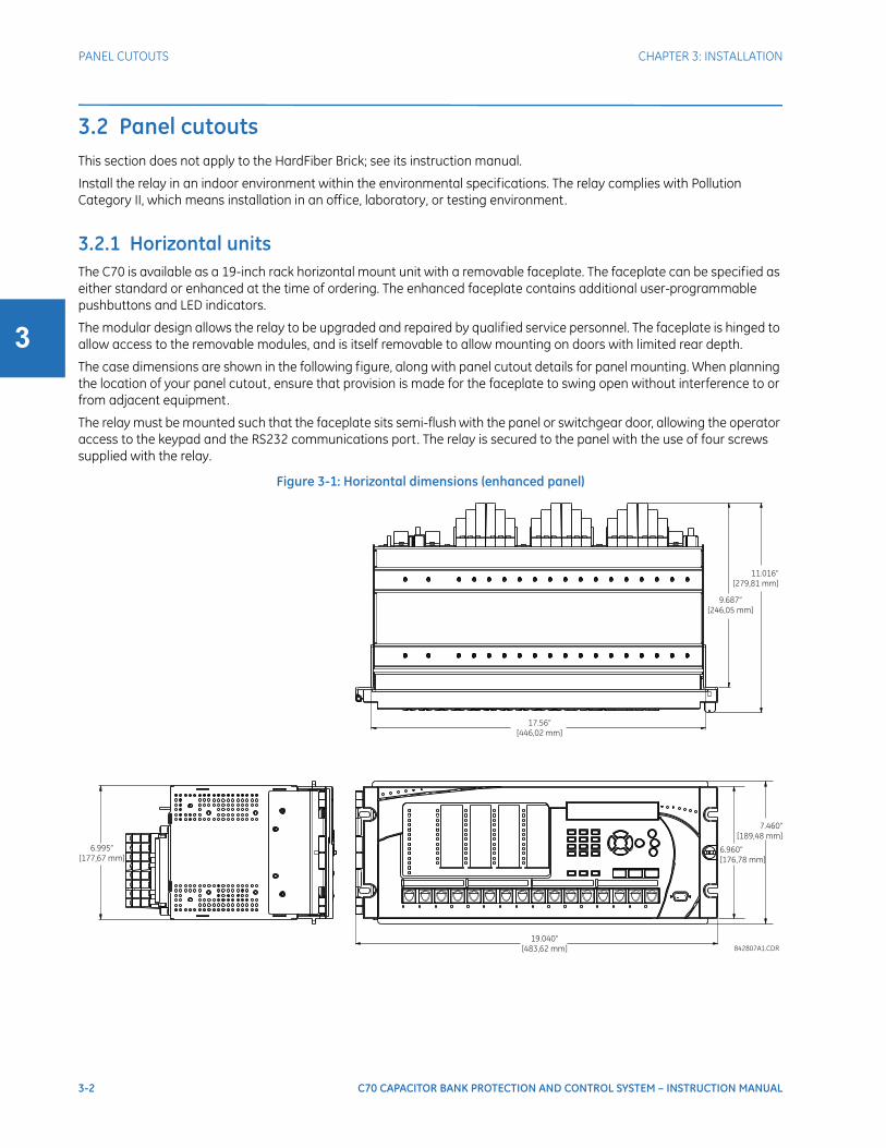
3-2 C70 CAPACITOR BANK PROTECTION AND CONTROL SYSTEM – INSTRUCTION MANUAL
PANEL CUTOUTS CHAPTER 3: INSTALLATION
3
3.2 Panel cutoutsThis section does not apply to the HardFiber Brick; see its instruction manual.
Install the relay in an indoor environment within the environmental specifications. The relay complies with Pollution Category II, which means installation in an office, laboratory, or testing environment.
3.2.1 Horizontal unitsThe C70 is available as a 19-inch rack horizontal mount unit with a removable faceplate. The faceplate can be specified as either standard or enhanced at the time of ordering. The enhanced faceplate contains additional user-programmable pushbuttons and LED indicators.
The modular design allows the relay to be upgraded and repaired by qualified service personnel. The faceplate is hinged to allow access to the removable modules, and is itself removable to allow mounting on doors with limited rear depth.
The case dimensions are shown in the following figure, along with panel cutout details for panel mounting. When planning the location of your panel cutout, ensure that provision is made for the faceplate to swing open without interference to or from adjacent equipment.
The relay must be mounted such that the faceplate sits semi-flush with the panel or switchgear door, allowing the operator access to the keypad and the RS232 communications port. The relay is secured to the panel with the use of four screws supplied with the relay.
Figure 3-1: Horizontal dimensions (enhanced panel)
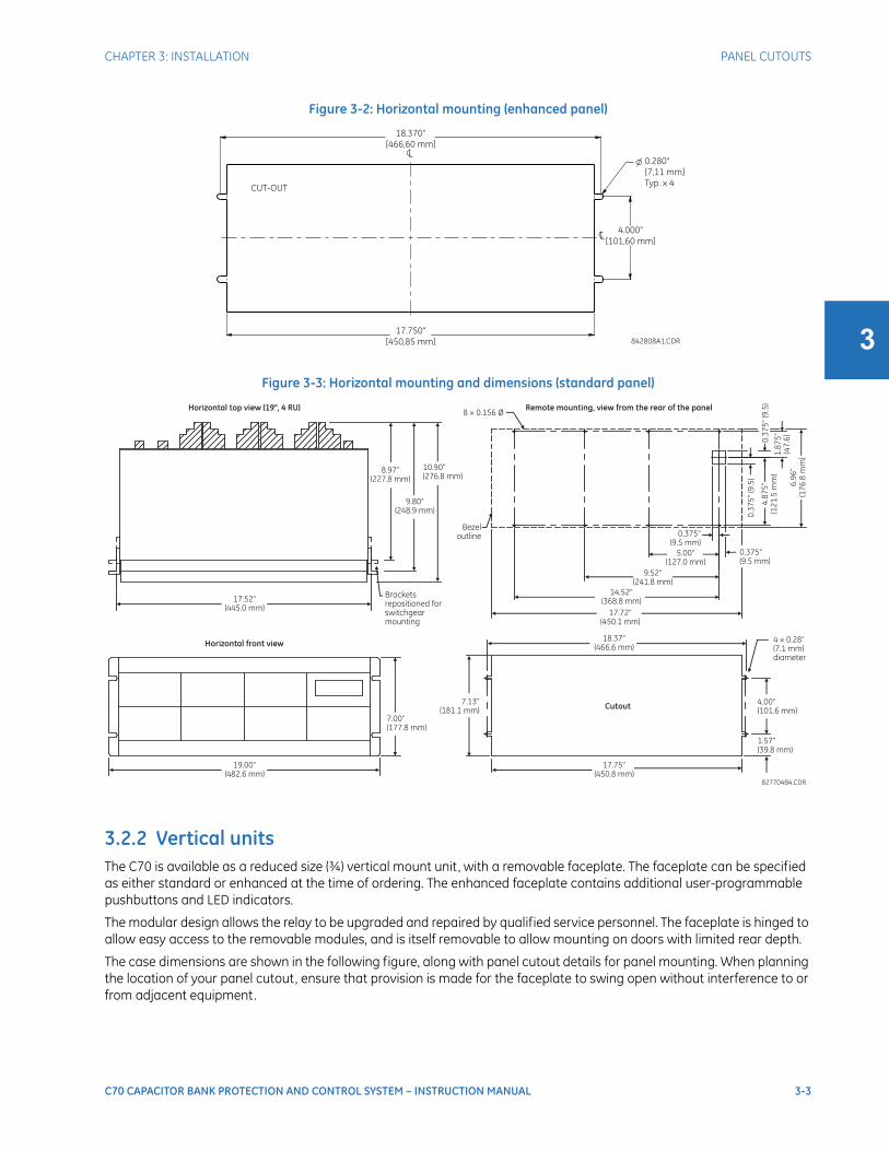
CHAPTER 3: INSTALLATION PANEL CUTOUTS
C70 CAPACITOR BANK PROTECTION AND CONTROL SYSTEM – INSTRUCTION MANUAL 3-3
3
Figure 3-2: Horizontal mounting (enhanced panel)
Figure 3-3: Horizontal mounting and dimensions (standard panel)
3.2.2 Vertical unitsThe C70 is available as a reduced size (¾) vertical mount unit, with a removable faceplate. The faceplate can be specified as either standard or enhanced at the time of ordering. The enhanced faceplate contains additional user-programmable pushbuttons and LED indicators.
The modular design allows the relay to be upgraded and repaired by qualified service personnel. The faceplate is hinged to allow easy access to the removable modules, and is itself removable to allow mounting on doors with limited rear depth.
The case dimensions are shown in the following figure, along with panel cutout details for panel mounting. When planning the location of your panel cutout, ensure that provision is made for the faceplate to swing open without interference to or from adjacent equipment.

3-4 C70 CAPACITOR BANK PROTECTION AND CONTROL SYSTEM – INSTRUCTION MANUAL
PANEL CUTOUTS CHAPTER 3: INSTALLATION
3
The relay must be mounted such that the faceplate sits semi-flush with the panel or switchgear door, allowing the operator access to the keypad and the RS232 communications port. The relay is secured to the panel with the use of four screws supplied with the relay.
Figure 3-4: Vertical dimensions (enhanced panel)
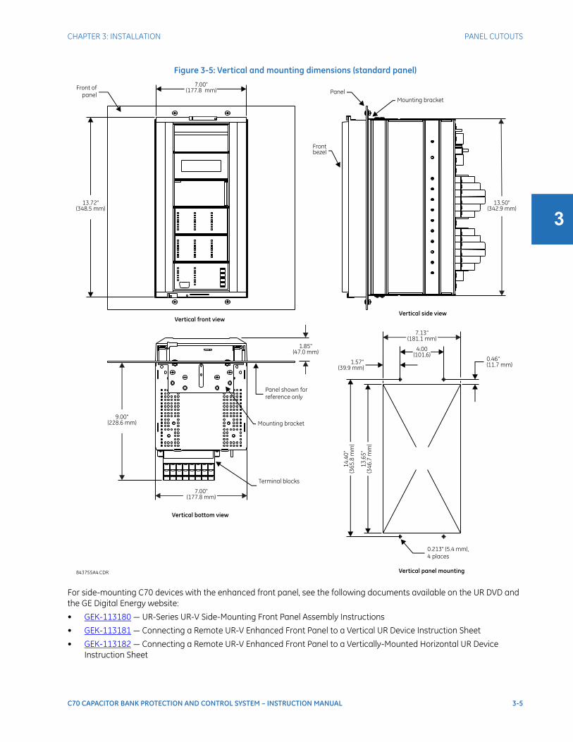
CHAPTER 3: INSTALLATION PANEL CUTOUTS
C70 CAPACITOR BANK PROTECTION AND CONTROL SYSTEM – INSTRUCTION MANUAL 3-5
3
Figure 3-5: Vertical and mounting dimensions (standard panel)
For side-mounting C70 devices with the enhanced front panel, see the following documents available on the UR DVD and the GE Digital Energy website:
• GEK-113180 — UR-Series UR-V Side-Mounting Front Panel Assembly Instructions
• GEK-113181 — Connecting a Remote UR-V Enhanced Front Panel to a Vertical UR Device Instruction Sheet
• GEK-113182 — Connecting a Remote UR-V Enhanced Front Panel to a Vertically-Mounted Horizontal UR Device Instruction Sheet

3-6 C70 CAPACITOR BANK PROTECTION AND CONTROL SYSTEM – INSTRUCTION MANUAL
PANEL CUTOUTS CHAPTER 3: INSTALLATION
3
For side-mounting C70 devices with the standard front panel, use the following figures.
Figure 3-6: Vertical side-mounting installation (standard panel)
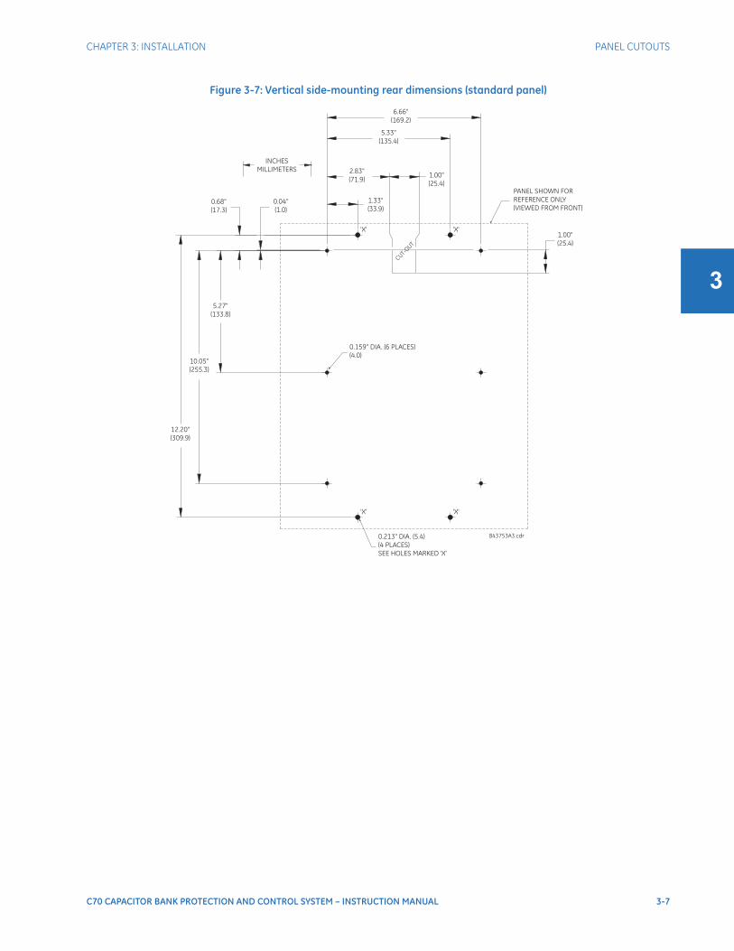
CHAPTER 3: INSTALLATION PANEL CUTOUTS
C70 CAPACITOR BANK PROTECTION AND CONTROL SYSTEM – INSTRUCTION MANUAL 3-7
3
Figure 3-7: Vertical side-mounting rear dimensions (standard panel)

3-8 C70 CAPACITOR BANK PROTECTION AND CONTROL SYSTEM – INSTRUCTION MANUAL
PANEL CUTOUTS CHAPTER 3: INSTALLATION
3
3.2.3 Rear terminal layout
The relay follows a convention with respect to terminal number assignments, which are three characters long and assigned by module slot position, row number, and column letter. Two-slot wide modules take their slot designation from the first slot position (nearest to CPU module), indicated by an arrow marker on the terminal block. The figure shows an example of rear terminal assignments.
Figure 3-8: Example of modules in F and H slots
Do not touch any rear terminals while the relay is energized, else death or serious injury can result from electrical shock.
The small form-factor pluggable ports (SFPs) are pluggable transceivers. Do not use non-validated transceivers or install validated transceivers in the wrong Ethernet slot, else damage can occur.
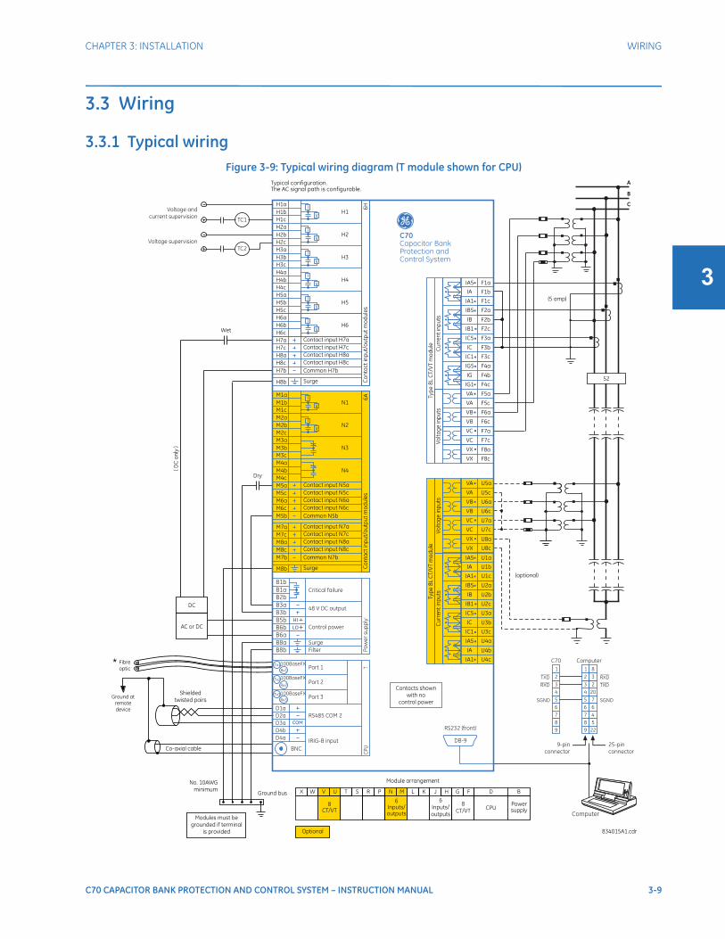
CHAPTER 3: INSTALLATION WIRING
C70 CAPACITOR BANK PROTECTION AND CONTROL SYSTEM – INSTRUCTION MANUAL 3-9
3
3.3 Wiring
3.3.1 Typical wiringFigure 3-9: Typical wiring diagram (T module shown for CPU)
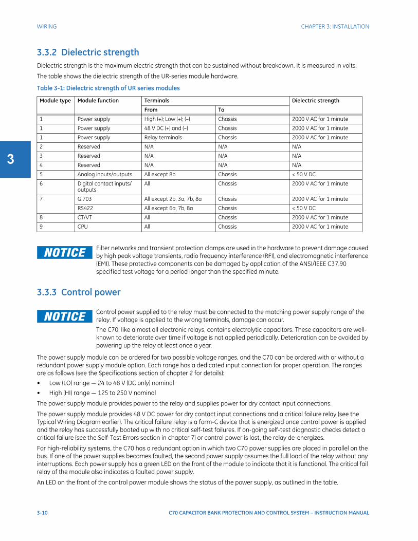
3-10 C70 CAPACITOR BANK PROTECTION AND CONTROL SYSTEM – INSTRUCTION MANUAL
WIRING CHAPTER 3: INSTALLATION
3
3.3.2 Dielectric strengthDielectric strength is the maximum electric strength that can be sustained without breakdown. It is measured in volts.
The table shows the dielectric strength of the UR-series module hardware.
Table 3-1: Dielectric strength of UR series modules
3.3.3 Control power
The power supply module can be ordered for two possible voltage ranges, and the C70 can be ordered with or without a redundant power supply module option. Each range has a dedicated input connection for proper operation. The ranges are as follows (see the Specifications section of chapter 2 for details):
• Low (LO) range — 24 to 48 V (DC only) nominal
• High (HI) range — 125 to 250 V nominal
The power supply module provides power to the relay and supplies power for dry contact input connections.
The power supply module provides 48 V DC power for dry contact input connections and a critical failure relay (see the Typical Wiring Diagram earlier). The critical failure relay is a form-C device that is energized once control power is applied and the relay has successfully booted up with no critical self-test failures. If on-going self-test diagnostic checks detect a critical failure (see the Self-Test Errors section in chapter 7) or control power is lost, the relay de-energizes.
For high-reliability systems, the C70 has a redundant option in which two C70 power supplies are placed in parallel on the bus. If one of the power supplies becomes faulted, the second power supply assumes the full load of the relay without any interruptions. Each power supply has a green LED on the front of the module to indicate that it is functional. The critical fail relay of the module also indicates a faulted power supply.
An LED on the front of the control power module shows the status of the power supply, as outlined in the table.
Module type Module function Terminals Dielectric strength
From To
1 Power supply High (+); Low (+); (–) Chassis 2000 V AC for 1 minute
1 Power supply 48 V DC (+) and (–) Chassis 2000 V AC for 1 minute
1 Power supply Relay terminals Chassis 2000 V AC for 1 minute
2 Reserved N/A N/A N/A
3 Reserved N/A N/A N/A
4 Reserved N/A N/A N/A
5 Analog inputs/outputs All except 8b Chassis < 50 V DC
6 Digital contact inputs/outputs
All Chassis 2000 V AC for 1 minute
7 G.703 All except 2b, 3a, 7b, 8a Chassis 2000 V AC for 1 minute
RS422 All except 6a, 7b, 8a Chassis < 50 V DC
8 CT/VT All Chassis 2000 V AC for 1 minute
9 CPU All Chassis 2000 V AC for 1 minute
Filter networks and transient protection clamps are used in the hardware to prevent damage caused by high peak voltage transients, radio frequency interference (RFI), and electromagnetic interference (EMI). These protective components can be damaged by application of the ANSI/IEEE C37.90 specified test voltage for a period longer than the specified minute.
Control power supplied to the relay must be connected to the matching power supply range of the relay. If voltage is applied to the wrong terminals, damage can occur.
The C70, like almost all electronic relays, contains electrolytic capacitors. These capacitors are well-known to deteriorate over time if voltage is not applied periodically. Deterioration can be avoided by powering up the relay at least once a year.

CHAPTER 3: INSTALLATION WIRING
C70 CAPACITOR BANK PROTECTION AND CONTROL SYSTEM – INSTRUCTION MANUAL 3-11
3
Table 3-2: Power supply LED on front panel
Figure 3-10: Control power connection
3.3.4 CT/VT modulesThe CT and VT inputs are analog current transformer and voltage transformer signals used to monitor AC power lines. The UR-series relays support 1 A and 5 A CTs.
A CT/VT module can have current or voltage inputs on channels 1 through 4 inclusive, or channels 5 through 8 inclusive. Channels 1 and 5 are intended for connection to phase A, and are labeled as such in the relay. Likewise, channels 2 and 6 are intended for connection to phase B, and channels 3 and 7 are intended for connection to phase C.
Channels 4 and 8 are intended for connection to a single-phase source. For voltage inputs, these channels are labeled as auxiliary voltage (VX). For current inputs, these channels are intended for connection to a CT between system neutral and ground, and are labelled as ground current (IG).
Verify that the connection made to the relay terminals for nominal current of 1 A or 5 A matches the secondary rating of the connected CTs. Unmatched CTs can result in equipment damage or inadequate protection.
To connect the module, size 12 American Wire Gauge (AWG) is used commonly; the maximum size is 10 AWG.
CT/VT modules can be ordered with a standard ground current input that is the same as the phase current input. Each AC current input has an isolating transformer and an automatic shorting mechanism that shorts the input when the module is withdrawn from the chassis. There are no internal ground connections on the current inputs. Current transformers with 1 to 50000 A primaries and 1 A or 5 A secondaries can be used.
These modules have enhanced diagnostics that can automatically detect CT/VT hardware failure and take the relay out of service.
CT connections for both ABC and ACB phase rotations are identical, as shown in the Typical Wiring Diagram.
The exact placement of a zero-sequence core balance CT to detect ground fault current is shown as follows. Twisted-pair cabling on the zero-sequence CT is recommended.
LED indication Power supply
Continuous on OK
On/off cycling Failure
Off Failure or no power

3-12 C70 CAPACITOR BANK PROTECTION AND CONTROL SYSTEM – INSTRUCTION MANUAL
WIRING CHAPTER 3: INSTALLATION
3
Figure 3-11: Zero-sequence core balance CT installation
The phase voltage channels are used for most metering and protection purposes. The auxiliary voltage channel is used as input for the synchrocheck and volts-per-hertz features, which are optional features available for some UR models.
Figure 3-12: CT/VT module wiring
NOTE
Substitute the tilde “~” symbol with the slot position of the module in the following figure.
842809A1.CDR
~ ~~~~~~~~~~~~~~~~~~~~~~~
1a
5a
1b
5b
1c
5c
2a
6a
2b
6b
2c
6c
3a
7a
4a
8a
3b
7b
4b
8b
3c
7c
4c
8c
Current inputs
IA IAIC ICIB IBIG IG
IA5
IA5
IC5
IC5
IB5
IB5
IG5
IG5
IA1
IA1
IC1
IC1
IB1
IB1
IG1
IG1
8H, 8J, 8N, and 8R modules (8 CTs)
~ ~~~~~~~~~~~~~~~~~~~
1a
1b
1c
2a
2b
2c
3a
4a
5a
6a
7a
8a
3b
4b
5c
6c
7c
8c
3c
4c
Current inputs
8F, 8G, 8L, and 8M modules (4 CTs and 4 VTs)
Voltage inputs
VA
VB
VC
VX
VA
VB
VC
VX
IA ICIB IG
IA5
IC5
IB5
IG5
IA1
IC1
IB1
IG1
~5
a
~6
a
~7
a
~8
a
~5
c
~6
c
~7
c
~8
c
8V modules (8 VTs)
VA
VB
VC
VX
VA
VB
VC
VX
~1
a
~2
a
~3
a
~4
a
~1
c
~2
c
~3
c
~4
c
VA
VB
VC
VX
VA
VB
VC
VX
Voltage inputs
~

CHAPTER 3: INSTALLATION WIRING
C70 CAPACITOR BANK PROTECTION AND CONTROL SYSTEM – INSTRUCTION MANUAL 3-13
3
3.3.5 Process bus modulesThe C70 can be ordered with a process bus interface module. The module interfaces with the HardFiber Process Bus System, or HardFiber Brick, allowing bidirectional IEC 61850 fiber optic communications with up to eight HardFiber Bricks. The HardFiber system integrates seamlessly with the existing UR-series applications, including protection functions, FlexLogic, metering, and communications.
This process bus system offers the following benefits:
• Reduces labor associated with design, installation, and testing of protection and control applications using the UR by reducing the number of individual copper terminations
• Integrates seamlessly with existing UR applications, since the IEC 61850 process bus interface module replaces the traditional CT/VT modules
• Communicates using open standard IEC 61850 messaging
For details on the HardFiber system, see its Instruction Manual.
3.3.6 Contact inputs and outputsEvery contact input/output module has 24 terminal connections. They are arranged as three terminals per row, with eight rows in total. A given row of three terminals can be used for the outputs of one relay. For example, for form-C relay outputs, the terminals connect to the normally open (NO), normally closed (NC), and common contacts of the relay. For a form-A output, there are options of using current or voltage detection for feature supervision, depending on the module ordered. The terminal configuration for contact inputs is different for the two applications.
The contact inputs are grouped with a common return. The C70 has two versions of grouping: four inputs per common return and two inputs per common return. When a contact input/output module is ordered, four inputs per common is used. If the inputs must be isolated per row, then two inputs per common return are selected (4D module).
The tables and diagrams on the following pages illustrate the module types (6A and so on) and contact arrangements that can be ordered for the relay. Since an entire row is used for a single contact output, the name is assigned using the module slot position and row number. However, since there are two contact inputs per row, these names are assigned by module slot position, row number, and column position.
Some form-A / solid-state relay outputs include circuits to monitor the DC voltage across the output contact when it is open, and the DC current through the output contact when it is closed. Each of the monitors contains a level detector whose output is set to logic “On = 1” when the current in the circuit is above the threshold setting. The voltage monitor is set to “On = 1” when there is a voltage across open contact (the detector allows a current of about 1 to 2.5 mA), and the current monitor is set to “On = 1” when the current flowing through the closed contact exceeds about 80 to 100 mA. The voltage monitor is intended to check the health of the overall trip circuit, and the current monitor can be used to seal-in the output contact until an external contact has interrupted current flow. If enabled, the current monitoring can be used as a seal-in signal to ensure that the form-A contact does not attempt to break the energized inductive coil circuit and weld the output contacts.
Block diagrams are shown as follows for form-A and solid-state relay outputs with optional voltage monitor, optional current monitor, and with no monitoring. The actual values shown for contact output 1 are the same for all contact outputs. Form-A contact output with or without a current or voltage monitoring option is not polarity sensitive. The polarity shown in the figure is required for solid-state contact output connection.
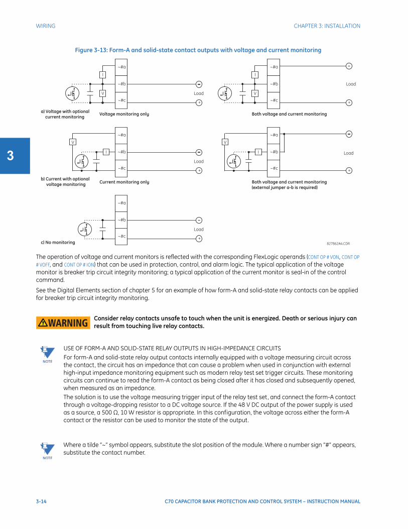
3-14 C70 CAPACITOR BANK PROTECTION AND CONTROL SYSTEM – INSTRUCTION MANUAL
WIRING CHAPTER 3: INSTALLATION
3
Figure 3-13: Form-A and solid-state contact outputs with voltage and current monitoring
The operation of voltage and current monitors is reflected with the corresponding FlexLogic operands (CONT OP # VON, CONT OP # VOFF, and CONT OP # ION) that can be used in protection, control, and alarm logic. The typical application of the voltage monitor is breaker trip circuit integrity monitoring; a typical application of the current monitor is seal-in of the control command.
See the Digital Elements section of chapter 5 for an example of how form-A and solid-state relay contacts can be applied for breaker trip circuit integrity monitoring.
Consider relay contacts unsafe to touch when the unit is energized. Death or serious injury can result from touching live relay contacts.
NOTE
USE OF FORM-A AND SOLID-STATE RELAY OUTPUTS IN HIGH-IMPEDANCE CIRCUITSFor form-A and solid-state relay output contacts internally equipped with a voltage measuring circuit across the contact, the circuit has an impedance that can cause a problem when used in conjunction with external high-input impedance monitoring equipment such as modern relay test set trigger circuits. These monitoring circuits can continue to read the form-A contact as being closed after it has closed and subsequently opened, when measured as an impedance.The solution is to use the voltage measuring trigger input of the relay test set, and connect the form-A contact through a voltage-dropping resistor to a DC voltage source. If the 48 V DC output of the power supply is used as a source, a 500 Ω, 10 W resistor is appropriate. In this configuration, the voltage across either the form-A contact or the resistor can be used to monitor the state of the output.
NOTE
Where a tilde “~” symbol appears, substitute the slot position of the module. Where a number sign “#” appears, substitute the contact number.
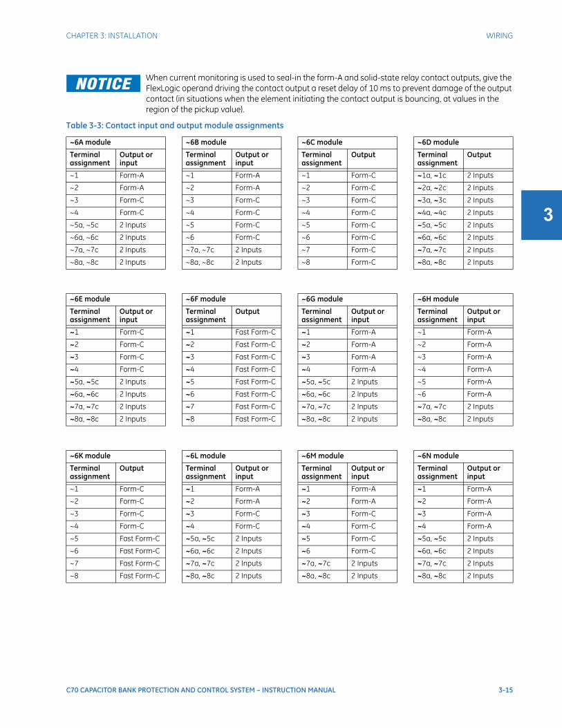
CHAPTER 3: INSTALLATION WIRING
C70 CAPACITOR BANK PROTECTION AND CONTROL SYSTEM – INSTRUCTION MANUAL 3-15
3
Table 3-3: Contact input and output module assignments
When current monitoring is used to seal-in the form-A and solid-state relay contact outputs, give the FlexLogic operand driving the contact output a reset delay of 10 ms to prevent damage of the output contact (in situations when the element initiating the contact output is bouncing, at values in the region of the pickup value).
~6A module ~6B module ~6C module ~6D module
Terminal assignment
Output or input
Terminal assignment
Output or input
Terminal assignment
Output Terminal assignment
Output
~1 Form-A ~1 Form-A ~1 Form-C ~1a, ~1c 2 Inputs
~2 Form-A ~2 Form-A ~2 Form-C ~2a, ~2c 2 Inputs
~3 Form-C ~3 Form-C ~3 Form-C ~3a, ~3c 2 Inputs
~4 Form-C ~4 Form-C ~4 Form-C ~4a, ~4c 2 Inputs
~5a, ~5c 2 Inputs ~5 Form-C ~5 Form-C ~5a, ~5c 2 Inputs
~6a, ~6c 2 Inputs ~6 Form-C ~6 Form-C ~6a, ~6c 2 Inputs
~7a, ~7c 2 Inputs ~7a, ~7c 2 Inputs ~7 Form-C ~7a, ~7c 2 Inputs
~8a, ~8c 2 Inputs ~8a, ~8c 2 Inputs ~8 Form-C ~8a, ~8c 2 Inputs
~6E module ~6F module ~6G module ~6H module
Terminal assignment
Output or input
Terminal assignment
Output Terminal assignment
Output or input
Terminal assignment
Output or input
~1 Form-C ~1 Fast Form-C ~1 Form-A ~1 Form-A
~2 Form-C ~2 Fast Form-C ~2 Form-A ~2 Form-A
~3 Form-C ~3 Fast Form-C ~3 Form-A ~3 Form-A
~4 Form-C ~4 Fast Form-C ~4 Form-A ~4 Form-A
~5a, ~5c 2 Inputs ~5 Fast Form-C ~5a, ~5c 2 Inputs ~5 Form-A
~6a, ~6c 2 Inputs ~6 Fast Form-C ~6a, ~6c 2 Inputs ~6 Form-A
~7a, ~7c 2 Inputs ~7 Fast Form-C ~7a, ~7c 2 Inputs ~7a, ~7c 2 Inputs
~8a, ~8c 2 Inputs ~8 Fast Form-C ~8a, ~8c 2 Inputs ~8a, ~8c 2 Inputs
~6K module ~6L module ~6M module ~6N module
Terminal assignment
Output Terminal assignment
Output or input
Terminal assignment
Output or input
Terminal assignment
Output or input
~1 Form-C ~1 Form-A ~1 Form-A ~1 Form-A
~2 Form-C ~2 Form-A ~2 Form-A ~2 Form-A
~3 Form-C ~3 Form-C ~3 Form-C ~3 Form-A
~4 Form-C ~4 Form-C ~4 Form-C ~4 Form-A
~5 Fast Form-C ~5a, ~5c 2 Inputs ~5 Form-C ~5a, ~5c 2 Inputs
~6 Fast Form-C ~6a, ~6c 2 Inputs ~6 Form-C ~6a, ~6c 2 Inputs
~7 Fast Form-C ~7a, ~7c 2 Inputs ~7a, ~7c 2 Inputs ~7a, ~7c 2 Inputs
~8 Fast Form-C ~8a, ~8c 2 Inputs ~8a, ~8c 2 Inputs ~8a, ~8c 2 Inputs
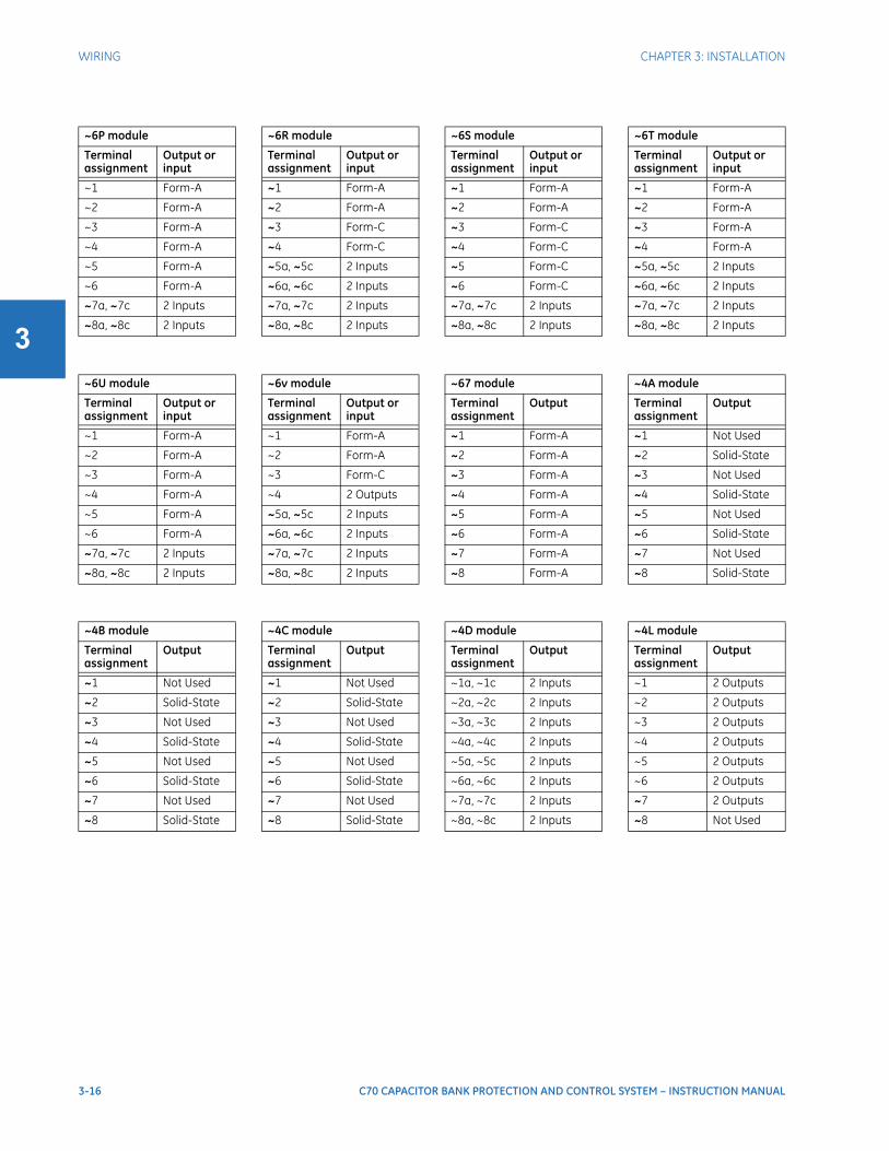
3-16 C70 CAPACITOR BANK PROTECTION AND CONTROL SYSTEM – INSTRUCTION MANUAL
WIRING CHAPTER 3: INSTALLATION
3
~6P module ~6R module ~6S module ~6T module
Terminal assignment
Output or input
Terminal assignment
Output or input
Terminal assignment
Output or input
Terminal assignment
Output or input
~1 Form-A ~1 Form-A ~1 Form-A ~1 Form-A
~2 Form-A ~2 Form-A ~2 Form-A ~2 Form-A
~3 Form-A ~3 Form-C ~3 Form-C ~3 Form-A
~4 Form-A ~4 Form-C ~4 Form-C ~4 Form-A
~5 Form-A ~5a, ~5c 2 Inputs ~5 Form-C ~5a, ~5c 2 Inputs
~6 Form-A ~6a, ~6c 2 Inputs ~6 Form-C ~6a, ~6c 2 Inputs
~7a, ~7c 2 Inputs ~7a, ~7c 2 Inputs ~7a, ~7c 2 Inputs ~7a, ~7c 2 Inputs
~8a, ~8c 2 Inputs ~8a, ~8c 2 Inputs ~8a, ~8c 2 Inputs ~8a, ~8c 2 Inputs
~6U module ~6v module ~67 module ~4A module
Terminal assignment
Output or input
Terminal assignment
Output or input
Terminal assignment
Output Terminal assignment
Output
~1 Form-A ~1 Form-A ~1 Form-A ~1 Not Used
~2 Form-A ~2 Form-A ~2 Form-A ~2 Solid-State
~3 Form-A ~3 Form-C ~3 Form-A ~3 Not Used
~4 Form-A ~4 2 Outputs ~4 Form-A ~4 Solid-State
~5 Form-A ~5a, ~5c 2 Inputs ~5 Form-A ~5 Not Used
~6 Form-A ~6a, ~6c 2 Inputs ~6 Form-A ~6 Solid-State
~7a, ~7c 2 Inputs ~7a, ~7c 2 Inputs ~7 Form-A ~7 Not Used
~8a, ~8c 2 Inputs ~8a, ~8c 2 Inputs ~8 Form-A ~8 Solid-State
~4B module ~4C module ~4D module ~4L module
Terminal assignment
Output Terminal assignment
Output Terminal assignment
Output Terminal assignment
Output
~1 Not Used ~1 Not Used ~1a, ~1c 2 Inputs ~1 2 Outputs
~2 Solid-State ~2 Solid-State ~2a, ~2c 2 Inputs ~2 2 Outputs
~3 Not Used ~3 Not Used ~3a, ~3c 2 Inputs ~3 2 Outputs
~4 Solid-State ~4 Solid-State ~4a, ~4c 2 Inputs ~4 2 Outputs
~5 Not Used ~5 Not Used ~5a, ~5c 2 Inputs ~5 2 Outputs
~6 Solid-State ~6 Solid-State ~6a, ~6c 2 Inputs ~6 2 Outputs
~7 Not Used ~7 Not Used ~7a, ~7c 2 Inputs ~7 2 Outputs
~8 Solid-State ~8 Solid-State ~8a, ~8c 2 Inputs ~8 Not Used
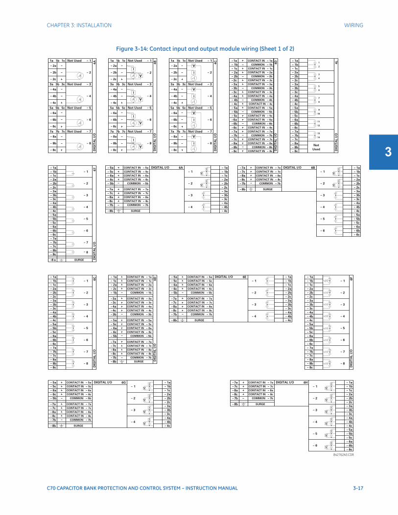
CHAPTER 3: INSTALLATION WIRING
C70 CAPACITOR BANK PROTECTION AND CONTROL SYSTEM – INSTRUCTION MANUAL 3-17
3
Figure 3-14: Contact input and output module wiring (Sheet 1 of 2)

3-18 C70 CAPACITOR BANK PROTECTION AND CONTROL SYSTEM – INSTRUCTION MANUAL
WIRING CHAPTER 3: INSTALLATION
3
Figure 3-15: Contact input and output module wiring (Sheet 2 of 2)
For proper functionality, observe the polarity shown in the figures for all contact input and output connections.

CHAPTER 3: INSTALLATION WIRING
C70 CAPACITOR BANK PROTECTION AND CONTROL SYSTEM – INSTRUCTION MANUAL 3-19
3
3.3.6.1 Contact inputsA dry contact has one side connected to terminal B3b. This is the positive 48 V DC voltage rail supplied by the power supply module. The other side of the dry contact is connected to the required contact input terminal. Each contact input group has its own common (negative) terminal that must be connected to the DC negative terminal (B3a) of the power supply module. When a dry contact closes, a current of 1 to 3 mA flows through the associated circuit.
A wet contact has one side connected to the positive terminal of an external DC power supply. The other side of this contact is connected to the required contact input terminal. If a wet contact is used, then the negative side of the external source must be connected to the relay common (negative) terminal of each contact group. The maximum external source voltage for this arrangement is 300 V DC.
The voltage threshold at which each group of four contact inputs detects a closed contact input is programmable as 17 V DC for 24 V sources, 33 V DC for 48 V sources, 84 V DC for 110 to 125 V sources, and 166 V DC for 250 V sources.
Figure 3-16: Dry and wet contact input connections
There is no provision in the relay to detect a DC ground fault on 48 V DC control power external output. We recommend using an external DC supply.
3.3.6.2 Use of contact inputs with auto-burnishingThe contact inputs sense a change of the state of the external device contact based on the measured current. When external devices are located in a harsh industrial environment (either outdoor or indoor), their contacts can be exposed to various types of contamination. Normally, there is a thin film of insulating sulfidation, oxidation, or contaminates on the surface of the contacts, sometimes making it difficult or impossible to detect a change of the state. This film must be removed to establish circuit continuity — an impulse of higher than normal current can accomplish this.
The contact inputs with auto-burnish create a high current impulse when the threshold is reached to burn off this oxidation layer as a maintenance to the contacts. Afterwards the contact input current is reduced to a steady-state current. The impulse has a five-second delay after a contact input changes state.
NOTE
Where a tilde “~” symbol appears, substitute the slot position of the module.
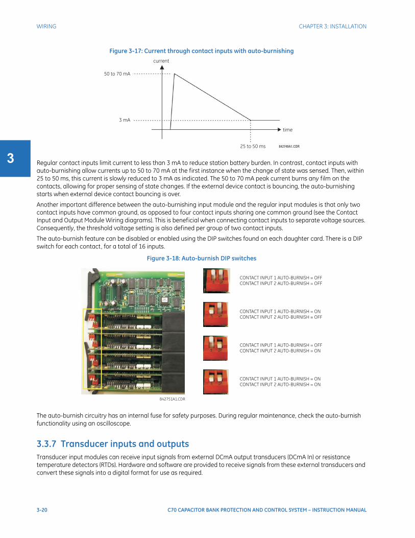
3-20 C70 CAPACITOR BANK PROTECTION AND CONTROL SYSTEM – INSTRUCTION MANUAL
WIRING CHAPTER 3: INSTALLATION
3
Figure 3-17: Current through contact inputs with auto-burnishing
Regular contact inputs limit current to less than 3 mA to reduce station battery burden. In contrast, contact inputs with auto-burnishing allow currents up to 50 to 70 mA at the first instance when the change of state was sensed. Then, within 25 to 50 ms, this current is slowly reduced to 3 mA as indicated. The 50 to 70 mA peak current burns any film on the contacts, allowing for proper sensing of state changes. If the external device contact is bouncing, the auto-burnishing starts when external device contact bouncing is over.
Another important difference between the auto-burnishing input module and the regular input modules is that only two contact inputs have common ground, as opposed to four contact inputs sharing one common ground (see the Contact Input and Output Module Wiring diagrams). This is beneficial when connecting contact inputs to separate voltage sources. Consequently, the threshold voltage setting is also defined per group of two contact inputs.
The auto-burnish feature can be disabled or enabled using the DIP switches found on each daughter card. There is a DIP switch for each contact, for a total of 16 inputs.
Figure 3-18: Auto-burnish DIP switches
The auto-burnish circuitry has an internal fuse for safety purposes. During regular maintenance, check the auto-burnish functionality using an oscilloscope.
3.3.7 Transducer inputs and outputsTransducer input modules can receive input signals from external DCmA output transducers (DCmA In) or resistance temperature detectors (RTDs). Hardware and software are provided to receive signals from these external transducers and convert these signals into a digital format for use as required.
842749A1.CDR
50 to 70 mA
3 mA
25 to 50 ms
current
time
CONTACT INPUT 1 AUTO-BURNISH = OFF= OFFCONTACT INPUT 2 AUTO-BURNISH
CONTACT INPUT 1 AUTO-BURNISHCONTACT INPUT 2 AUTO-BURNISH
= ON= OFF
CONTACT INPUT 1 AUTO-BURNISHCONTACT INPUT 2 AUTO-BURNISH
= OFF= ON
CONTACT INPUT 1 AUTO-BURNISHCONTACT INPUT 2 AUTO-BURNISH
= ON= ON
842751A1.CDR

CHAPTER 3: INSTALLATION WIRING
C70 CAPACITOR BANK PROTECTION AND CONTROL SYSTEM – INSTRUCTION MANUAL 3-21
3
Transducer output modules provide DC current outputs in several standard DCmA ranges. Software is provided to configure virtually any analog quantity used in the relay to drive the analog outputs.
Every transducer input/output module has a total of 24 terminal connections. These connections are arranged as three terminals per row with a total of eight rows. A given row can be used for either inputs or outputs, with terminals in column "a" having positive polarity and terminals in column "c" having negative polarity. Since an entire row is used for a single input/output channel, the name of the channel is assigned using the module slot position and row number.
Each module also requires that a connection from an external ground bus be made to terminal 8b. The current outputs require a twisted-pair shielded cable, where the shield is grounded at one end only. The following figure illustrates the transducer module types (5A, 5C, 5D, 5E, and 5F) and channel arrangements that can be ordered for the relay.
Figure 3-19: Transducer input/output module wiring
The following figure show how to connect RTDs.
NOTE
Where a tilde “~” symbol appears, substitute the slot position of the module.

3-22 C70 CAPACITOR BANK PROTECTION AND CONTROL SYSTEM – INSTRUCTION MANUAL
WIRING CHAPTER 3: INSTALLATION
3
Figure 3-20: RTD connections
3.3.8 RS232 faceplate portA nine-pin RS232C serial port is located on the faceplate for programming with a computer. All that is required to use this interface is a computer running the EnerVista UR Setup software provided with the relay. Cabling for the RS232 port is shown in the following figure for both 9-pin and 25-pin connectors.
The baud rate for this port can be set, with a default of 115200 bps.
Figure 3-21: RS232 faceplate port connection
3.3.9 CPU communication ports
3.3.9.1 OverviewIn addition to the faceplate RS232 port, there is a rear RS485 communication port.
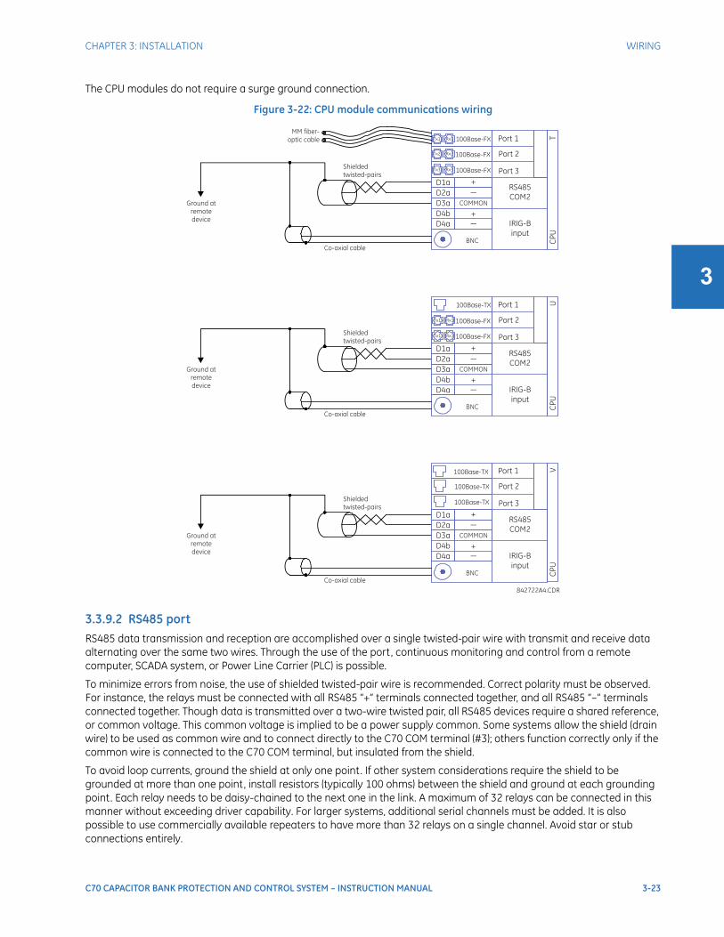
CHAPTER 3: INSTALLATION WIRING
C70 CAPACITOR BANK PROTECTION AND CONTROL SYSTEM – INSTRUCTION MANUAL 3-23
3
The CPU modules do not require a surge ground connection.
Figure 3-22: CPU module communications wiring
3.3.9.2 RS485 portRS485 data transmission and reception are accomplished over a single twisted-pair wire with transmit and receive data alternating over the same two wires. Through the use of the port, continuous monitoring and control from a remote computer, SCADA system, or Power Line Carrier (PLC) is possible.
To minimize errors from noise, the use of shielded twisted-pair wire is recommended. Correct polarity must be observed. For instance, the relays must be connected with all RS485 “+” terminals connected together, and all RS485 “–” terminals connected together. Though data is transmitted over a two-wire twisted pair, all RS485 devices require a shared reference, or common voltage. This common voltage is implied to be a power supply common. Some systems allow the shield (drain wire) to be used as common wire and to connect directly to the C70 COM terminal (#3); others function correctly only if the common wire is connected to the C70 COM terminal, but insulated from the shield.
To avoid loop currents, ground the shield at only one point. If other system considerations require the shield to be grounded at more than one point, install resistors (typically 100 ohms) between the shield and ground at each grounding point. Each relay needs to be daisy-chained to the next one in the link. A maximum of 32 relays can be connected in this manner without exceeding driver capability. For larger systems, additional serial channels must be added. It is also possible to use commercially available repeaters to have more than 32 relays on a single channel. Avoid star or stub connections entirely.
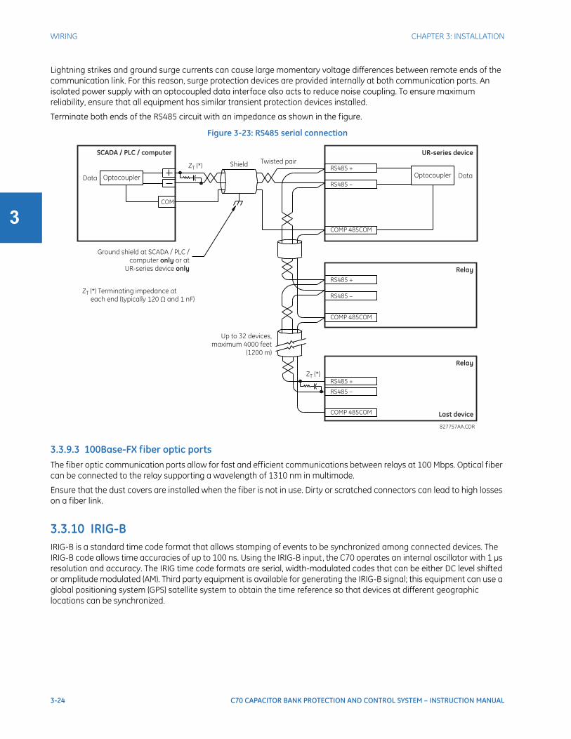
3-24 C70 CAPACITOR BANK PROTECTION AND CONTROL SYSTEM – INSTRUCTION MANUAL
WIRING CHAPTER 3: INSTALLATION
3
Lightning strikes and ground surge currents can cause large momentary voltage differences between remote ends of the communication link. For this reason, surge protection devices are provided internally at both communication ports. An isolated power supply with an optocoupled data interface also acts to reduce noise coupling. To ensure maximum reliability, ensure that all equipment has similar transient protection devices installed.
Terminate both ends of the RS485 circuit with an impedance as shown in the figure.
Figure 3-23: RS485 serial connection
3.3.9.3 100Base-FX fiber optic portsThe fiber optic communication ports allow for fast and efficient communications between relays at 100 Mbps. Optical fiber can be connected to the relay supporting a wavelength of 1310 nm in multimode.
Ensure that the dust covers are installed when the fiber is not in use. Dirty or scratched connectors can lead to high losses on a fiber link.
3.3.10 IRIG-BIRIG-B is a standard time code format that allows stamping of events to be synchronized among connected devices. The IRIG-B code allows time accuracies of up to 100 ns. Using the IRIG-B input, the C70 operates an internal oscillator with 1 µs resolution and accuracy. The IRIG time code formats are serial, width-modulated codes that can be either DC level shifted or amplitude modulated (AM). Third party equipment is available for generating the IRIG-B signal; this equipment can use a global positioning system (GPS) satellite system to obtain the time reference so that devices at different geographic locations can be synchronized.

CHAPTER 3: INSTALLATION DIRECT INPUT AND OUTPUT COMMUNICATIONS
C70 CAPACITOR BANK PROTECTION AND CONTROL SYSTEM – INSTRUCTION MANUAL 3-25
3
Figure 3-24: Options for the IRIG-B connection
3.4 Direct input and output communications
3.4.1 DescriptionThe direct inputs and outputs feature makes use of the type 7 series of communications modules and allows direct messaging between UR devices. The communications modules are outlined in the table later in this section.
The communications channels are normally connected in a ring configuration, as shown in the following figure. The transmitter of one module is connected to the receiver of the next module. The transmitter of this second module is then connected to the receiver of the next module in the ring. This is continued to form a communications ring. The figure illustrates a ring of four UR-series relays with the following connections: UR1-Tx to UR2-Rx, UR2-Tx to UR3-Rx, UR3-Tx to UR4-Rx, and UR4-Tx to UR1-Rx. A maximum of 16 UR-series relays can be connected in a single ring.
NOTE
Using an amplitude-modulated receiver causes errors up to 1 ms in event time-stamping.
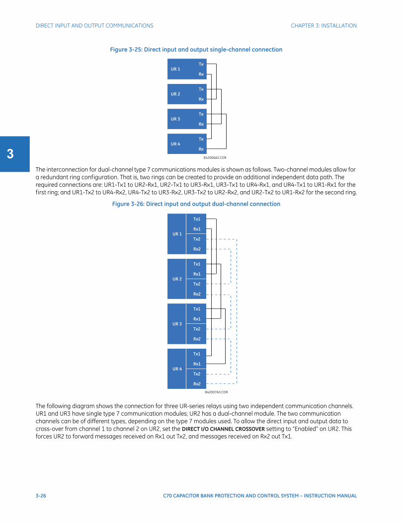
3-26 C70 CAPACITOR BANK PROTECTION AND CONTROL SYSTEM – INSTRUCTION MANUAL
DIRECT INPUT AND OUTPUT COMMUNICATIONS CHAPTER 3: INSTALLATION
3
Figure 3-25: Direct input and output single-channel connection
The interconnection for dual-channel type 7 communications modules is shown as follows. Two-channel modules allow for a redundant ring configuration. That is, two rings can be created to provide an additional independent data path. The required connections are: UR1-Tx1 to UR2-Rx1, UR2-Tx1 to UR3-Rx1, UR3-Tx1 to UR4-Rx1, and UR4-Tx1 to UR1-Rx1 for the first ring; and UR1-Tx2 to UR4-Rx2, UR4-Tx2 to UR3-Rx2, UR3-Tx2 to UR2-Rx2, and UR2-Tx2 to UR1-Rx2 for the second ring.
Figure 3-26: Direct input and output dual-channel connection
The following diagram shows the connection for three UR-series relays using two independent communication channels. UR1 and UR3 have single type 7 communication modules; UR2 has a dual-channel module. The two communication channels can be of different types, depending on the type 7 modules used. To allow the direct input and output data to cross-over from channel 1 to channel 2 on UR2, set the DIRECT I/O CHANNEL CROSSOVER setting to “Enabled” on UR2. This forces UR2 to forward messages received on Rx1 out Tx2, and messages received on Rx2 out Tx1.
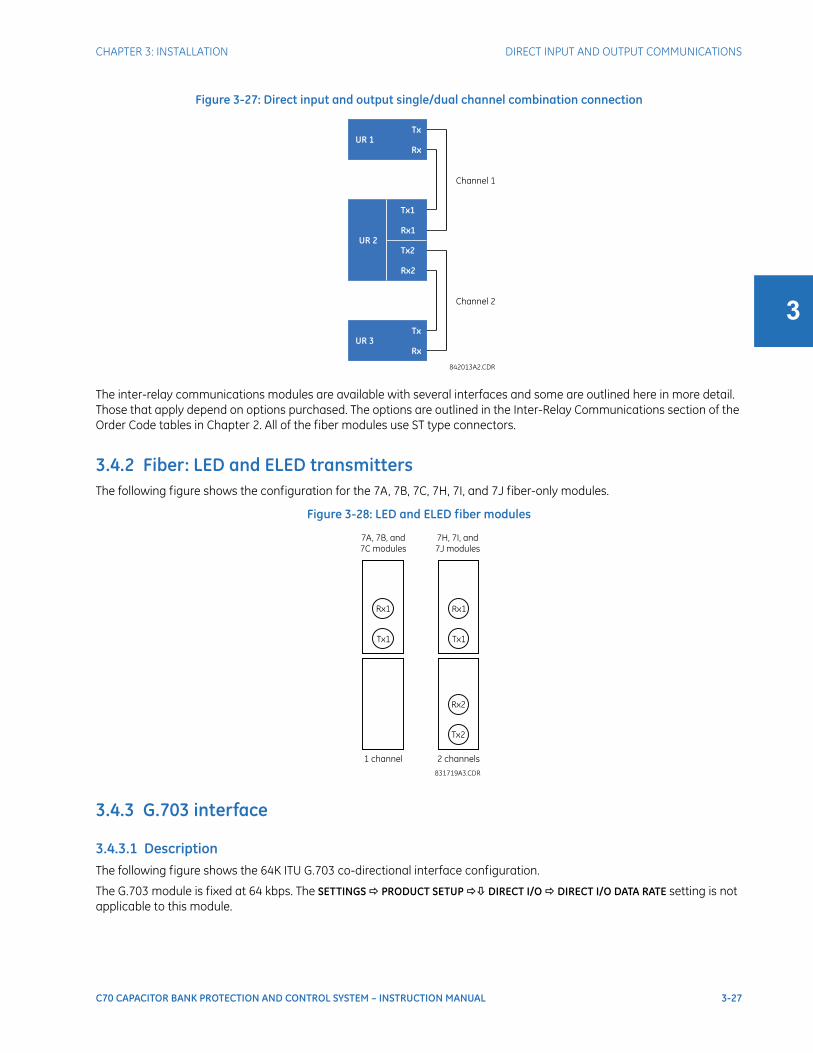
CHAPTER 3: INSTALLATION DIRECT INPUT AND OUTPUT COMMUNICATIONS
C70 CAPACITOR BANK PROTECTION AND CONTROL SYSTEM – INSTRUCTION MANUAL 3-27
3
Figure 3-27: Direct input and output single/dual channel combination connection
The inter-relay communications modules are available with several interfaces and some are outlined here in more detail. Those that apply depend on options purchased. The options are outlined in the Inter-Relay Communications section of the Order Code tables in Chapter 2. All of the fiber modules use ST type connectors.
3.4.2 Fiber: LED and ELED transmittersThe following figure shows the configuration for the 7A, 7B, 7C, 7H, 7I, and 7J fiber-only modules.
Figure 3-28: LED and ELED fiber modules
3.4.3 G.703 interface
3.4.3.1 DescriptionThe following figure shows the 64K ITU G.703 co-directional interface configuration.
The G.703 module is fixed at 64 kbps. The SETTINGS PRODUCT SETUP DIRECT I/O DIRECT I/O DATA RATE setting is not applicable to this module.
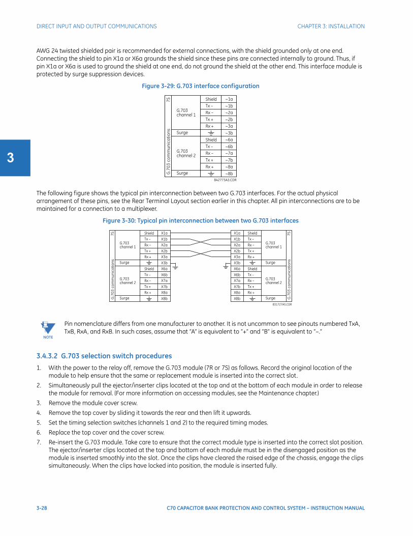
3-28 C70 CAPACITOR BANK PROTECTION AND CONTROL SYSTEM – INSTRUCTION MANUAL
DIRECT INPUT AND OUTPUT COMMUNICATIONS CHAPTER 3: INSTALLATION
3
AWG 24 twisted shielded pair is recommended for external connections, with the shield grounded only at one end. Connecting the shield to pin X1a or X6a grounds the shield since these pins are connected internally to ground. Thus, if pin X1a or X6a is used to ground the shield at one end, do not ground the shield at the other end. This interface module is protected by surge suppression devices.
Figure 3-29: G.703 interface configuration
The following figure shows the typical pin interconnection between two G.703 interfaces. For the actual physical arrangement of these pins, see the Rear Terminal Layout section earlier in this chapter. All pin interconnections are to be maintained for a connection to a multiplexer.
Figure 3-30: Typical pin interconnection between two G.703 interfaces
3.4.3.2 G.703 selection switch procedures
1. With the power to the relay off, remove the G.703 module (7R or 7S) as follows. Record the original location of the module to help ensure that the same or replacement module is inserted into the correct slot.
2. Simultaneously pull the ejector/inserter clips located at the top and at the bottom of each module in order to release the module for removal. (For more information on accessing modules, see the Maintenance chapter.)
3. Remove the module cover screw.
4. Remove the top cover by sliding it towards the rear and then lift it upwards.
5. Set the timing selection switches (channels 1 and 2) to the required timing modes.
6. Replace the top cover and the cover screw.
7. Re-insert the G.703 module. Take care to ensure that the correct module type is inserted into the correct slot position. The ejector/inserter clips located at the top and bottom of each module must be in the disengaged position as the module is inserted smoothly into the slot. Once the clips have cleared the raised edge of the chassis, engage the clips simultaneously. When the clips have locked into position, the module is inserted fully.
NOTE
Pin nomenclature differs from one manufacturer to another. It is not uncommon to see pinouts numbered TxA, TxB, RxA, and RxB. In such cases, assume that “A” is equivalent to “+” and “B” is equivalent to “–.”

CHAPTER 3: INSTALLATION DIRECT INPUT AND OUTPUT COMMUNICATIONS
C70 CAPACITOR BANK PROTECTION AND CONTROL SYSTEM – INSTRUCTION MANUAL 3-29
3
Figure 3-31: G.703 timing selection switch setting
Table 3-4: G.703 timing selections
3.4.3.3 G.703 octet timingIf octet timing is enabled (ON), this 8 kHz signal is asserted during the violation of bit 8 (LSB) necessary for connecting to higher order systems. When C70s are connected back-to-back, octet timing is disabled (OFF).
3.4.3.4 G.703 timing modesThere are two timing modes for the G.703 module: internal timing mode and loop timing mode (default).
• Internal Timing Mode — The system clock is generated internally. Therefore, set the G.703 timing selection to internal timing mode for back-to-back (UR-to-UR) connections. For back-to-back connections, set octet timing (S1 = OFF) and timing mode to internal timing (S5 = ON and S6 = OFF).
• Loop Timing Mode — The system clock is derived from the received line signal. Therefore, set the G.703 timing selection to loop timing mode for connections to higher order systems. For connection to a higher order system (UR-to-multiplexer, factory defaults), set to octet timing (S1 = ON) and set timing mode to loop timing (S5 = OFF and S6 = OFF).
The switch settings for the internal and loop timing modes are shown.
Switches Function
S1 OFF → octet timing disabledON → octet timing 8 kHz
S5 and S6 S5 = OFF and S6 = OFF → loop timing modeS5 = ON and S6 = OFF → internal timing modeS5 = OFF and S6 = ON → minimum remote loopback modeS5 = ON and S6 = ON → dual loopback mode
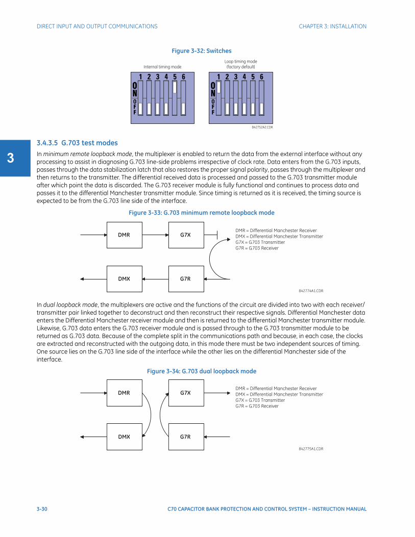
3-30 C70 CAPACITOR BANK PROTECTION AND CONTROL SYSTEM – INSTRUCTION MANUAL
DIRECT INPUT AND OUTPUT COMMUNICATIONS CHAPTER 3: INSTALLATION
3
Figure 3-32: Switches
3.4.3.5 G.703 test modesIn minimum remote loopback mode, the multiplexer is enabled to return the data from the external interface without any processing to assist in diagnosing G.703 line-side problems irrespective of clock rate. Data enters from the G.703 inputs, passes through the data stabilization latch that also restores the proper signal polarity, passes through the multiplexer and then returns to the transmitter. The differential received data is processed and passed to the G.703 transmitter module after which point the data is discarded. The G.703 receiver module is fully functional and continues to process data and passes it to the differential Manchester transmitter module. Since timing is returned as it is received, the timing source is expected to be from the G.703 line side of the interface.
Figure 3-33: G.703 minimum remote loopback mode
In dual loopback mode, the multiplexers are active and the functions of the circuit are divided into two with each receiver/transmitter pair linked together to deconstruct and then reconstruct their respective signals. Differential Manchester data enters the Differential Manchester receiver module and then is returned to the differential Manchester transmitter module. Likewise, G.703 data enters the G.703 receiver module and is passed through to the G.703 transmitter module to be returned as G.703 data. Because of the complete split in the communications path and because, in each case, the clocks are extracted and reconstructed with the outgoing data, in this mode there must be two independent sources of timing. One source lies on the G.703 line side of the interface while the other lies on the differential Manchester side of the interface.
Figure 3-34: G.703 dual loopback mode
DMR
DMX
G7X
G7R
DMR = Differential Manchester Receiver
DMX = Differential Manchester Transmitter
G7X = G.703 Transmitter
G7R = G.703 Receiver
842774A1.CDR
DMR
DMX
G7X
G7R
DMR = Differential Manchester Receiver
DMX = Differential Manchester Transmitter
G7X = G.703 Transmitter
G7R = G.703 Receiver
842775A1.CDR

CHAPTER 3: INSTALLATION DIRECT INPUT AND OUTPUT COMMUNICATIONS
C70 CAPACITOR BANK PROTECTION AND CONTROL SYSTEM – INSTRUCTION MANUAL 3-31
3
3.4.4 RS422 interface
3.4.4.1 DescriptionThere are two RS422 inter-relay communications modules available: single-channel RS422 (module 7T) and dual-channel RS422 (module 7W). The modules can be configured to run at 64 kbps or 128 kbps. AWG 20-24 twisted shielded pair cable is recommended for external connections. These modules are protected by optically-isolated surge suppression devices.
The shield pins (6a and 7b) are connected internally to the ground pin (8a). Proper shield termination is as follows:
• Site 1 — Terminate shield to pins 6a or 7b or both
• Site 2 — Terminate shield to COM pin 2b
Match the clock terminating impedance with the impedance of the line.
Figure 3-35: RS422 interface connections
The following figure shows the typical pin interconnection between two single-channel RS422 interfaces installed in slot W. All pin interconnections are to be maintained for a connection to a multiplexer.
Figure 3-36: Typical pin interconnect between two RS422 interfaces
3.4.4.2 Two-channel application via multiplexersThe RS422 interface can be used for single-channel or two-channel applications over SONET/SDH or multiplexed systems. When used in single-channel applications, the RS422 interface links to higher-order systems in a typical way, observing transmit (Tx), receive (Rx), and send timing (ST) connections. However, when used in two-channel applications, certain criteria must be followed since there is one clock input for the two RS422 channels. The system functions correctly when the following connections are observed and your data module has a terminal timing feature. Terminal timing is a common feature to most synchronous data units that allows the module to accept timing from an external source. Using the terminal timing feature, two-channel applications can be achieved if these connections are followed: the send timing outputs from the multiplexer (data module 1) connects to the clock inputs of the UR RS422 interface in the usual way. In addition, the send timing outputs of data module 1 are also paralleled to the terminal timing inputs of data module 2. By using this configuration, the timing for both data modules and both UR RS422 channels are derived from a single clock
~
~
~
~
~
~
~
~
~
~
~
~
~
~
Shield
Shield
COM
Tx +
Tx +
Tx –
Tx –
Rx –
Rx –
Rx +
Rx +
3b
5b
2a
4a
6a
7b
8bClock
RS422
channel 1
RS422
channel 2
Surge
3a
5a
4b
6b
7a
2b
8a Inte
r-re
lay
co
mm
un
ica
tio
ns
7W
842776A3.CDR
Dual-channel RS422 module
~
~
~
~
~
Shield
Tx +
Tx –
Rx –
Rx +
3b
2a
6a
RS422
3a
4b
~
~
~
~
COM
8bClock
Surge
7a
2b
8a Inte
r-re
lay
co
mm
s.
7T
Single-channel RS422 module
~ indicates the slot position

3-32 C70 CAPACITOR BANK PROTECTION AND CONTROL SYSTEM – INSTRUCTION MANUAL
DIRECT INPUT AND OUTPUT COMMUNICATIONS CHAPTER 3: INSTALLATION
3
source. As a result, data sampling for both of the UR RS422 channels is synchronized via the send timing leads on data module 1, shown as follows. If the terminal timing feature is not available or this type of connection is not wanted, the G.703 interface is a viable option that does not impose timing restrictions.
Figure 3-37: Timing configuration for RS422 two-channel, three-terminal application
Data module 1 provides timing to the C70 RS422 interface via the ST(A) and ST(B) outputs. Data module 1 also provides timing to data module 2 TT(A) and TT(B) inputs via the ST(A) and AT(B) outputs. The data module pin numbers have been omitted in the figure because they vary by manufacturer.
3.4.4.3 Transmit timingThe RS422 interface accepts one clock input for transmit timing. It is important that the rising edge of the 64 kHz transmit timing clock of the multiplexer interface is sampling the data in the center of the transmit data window. Therefore, it is important to confirm clock and data transitions to ensure proper system operation. For example, the following figure shows the positive edge of the Tx clock in the center of the Tx data bit.
Figure 3-38: Clock and data transitions
Data module 1
Data module 2
Signal name
Signal name
SD(A) - Send data
TT(A) - Terminal timing
TT(B) - Terminal timing
SD(B) - Send data
RD(A) - Received data
RD(A) - Received data
SD(A) - Send data
SD(B) - Send data
RD(B) - Received data
RD(B) - Received data
RS(A) - Request to send (RTS)
RS(A) - Request to send (RTS)
RT(A) - Receive timing
CS(A) - Clear To send
CS(A) - Clear To send
RT(B) - Receive timing
CS(B) - Clear To send
CS(B) - Clear To send
Local loopback
Local loopback
Remote loopback
Remote loopback
Signal ground
Signal ground
ST(A) - Send timing
ST(A) - Send timing
ST(B) - Send timing
ST(B) - Send timing
RS(B) - Request to send (RTS)
RS(B) - Request to send (RTS)
831022A3.CDR
W7a
W2b
W8a
7W
Shld.
Shld.
Tx1(+)
Tx2(+)
Tx1(-)
Tx2(-)
Rx1(+)
Rx2(+)
+
com
Rx1(-)
Rx2(-)
–
INT
ER
-R
EL
AY
CO
MM
UN
ICA
TIO
NS
W3a
W5b
W5a
W3b
W2a
W6a
W6b
W7b
W8b
W4b
W4a
RS422
CHANNEL 1
RS422
CHANNEL 2
CLOCK
SURGE
831733A1.CDR
Tx Clock
Tx Data

CHAPTER 3: INSTALLATION DIRECT INPUT AND OUTPUT COMMUNICATIONS
C70 CAPACITOR BANK PROTECTION AND CONTROL SYSTEM – INSTRUCTION MANUAL 3-33
3
3.4.4.4 Receive timingThe RS422 interface utilizes NRZI-MARK modulation code and therefore does not rely on an Rx clock to recapture data. NRZI-MARK is an edge-type, invertible, self-clocking code.
To recover the Rx clock from the data-stream, an integrated digital phase lock loop (DPLL) circuit is utilized. The DPLL is driven by an internal clock, which is 16-times over-sampled, and uses this clock along with the data-stream to generate a data clock that can be used as the serial communication controller (SCC) receive clock.
3.4.5 IEEE C37.94 interfaceThe UR-series IEEE C37.94 communication modules (module types 2I, 2J, 76, and 77) are designed to interface with IEEE C37.94 compliant digital multiplexers or an IEEE C37.94 compliant interface converter for use with direct input and output applications. The IEEE C37.94 standard defines a point-to-point optical link for synchronous data between a multiplexer and a teleprotection device. This data is typically 64 kbps, but the standard provides for speeds up to 64n kbps, where n = 1, 2,…, 12. The UR-series C37.94 communication modules are either 64 kbps (with n fixed at 1) for 128 kbps (with n fixed at 2). The frame is a valid International Telecommunications Union (ITU-T) recommended G.704 pattern from the standpoint of framing and data rate. The frame is 256 bits and is repeated at a frame rate of 8000 Hz, with a resultant bit rate of 2048 kbps.
The specifications for the module are as follows:
• IEEE standard — C37.94 for 2 × 64 kbps optical fiber interface (for 76 and 77 modules)
• Fiber optic cable type — 50 nm or 62.5 μm core diameter optical fiber
• Fiber optic mode — multimode
• Fiber optic cable length — up to 2 km
• Fiber optic connector — type ST
• Wavelength — 820 ±40 nm
• Connection — as per all fiber optic connections, a Tx to Rx connection is required
The UR-series C37.94 communication module can be connected directly to any compliant digital multiplexer that supports the IEEE C37.94 standard. The figure shows the concept.
Figure 3-39: IEEE C37.94 connection to compliant digital multiplexer
The UR-series C37.94 communication module can be connected to the electrical interface (G.703, RS422, or X.21) of a non-compliant digital multiplexer via an optical-to-electrical interface converter that supports the IEEE C37.94 standard. The following figure shows the concept.
Figure 3-40: IEEE C37.94 connection to non-compliant digital multiplexer

3-34 C70 CAPACITOR BANK PROTECTION AND CONTROL SYSTEM – INSTRUCTION MANUAL
DIRECT INPUT AND OUTPUT COMMUNICATIONS CHAPTER 3: INSTALLATION
3
In 2008, GE Digital Energy released revised modules 76 and 77 for C37.94 communication to enable multi-ended fault location functionality with firmware 5.60 release and higher. All modules 76 and 77 shipped since the change support this feature and are fully backward compatible with firmware releases below 5.60. For customers using firmware release 5.60 and higher, the module can be identified with "Rev D" printed on the module and is to be used on all ends of C70 communication for two and three terminal applications. Failure to use it at all ends results in intermittent communication alarms. For customers using firmware revisions below 5.60, it is not required to match the revision of the modules installed.
The UR-series C37.94 communication module has six switches to set the clock configuration. The following figure shows the functions of these control switches.
Figure 3-41: Switches
For the internal timing mode, the system clock is generated internally. Therefore, set the timing switch selection to internal timing for relay 1 and loop timed for relay 2. There must be only one timing source configured.
For the looped timing mode, the system clock is derived from the received line signal. Therefore, set the timing selection to loop timing mode for connections to higher order systems.
The IEEE C37.94 communications module cover removal procedure is as follows:
1. With power to the relay off, remove the IEEE C37.94 module (type 2I, 2J, 76, or 77 module) as follows. Record the original location of the module to help ensure that the same or replacement module is inserted into the correct slot.
2. Simultaneously pull the ejector/inserter clips located at the top and bottom of each module in order to release the module for removal.
3. Remove the module cover screw.
4. Remove the top cover by sliding it towards the rear and then lift it upwards.
5. Set the timing selection switches (channels 1 and 2) to the required timing modes (see description earlier).
6. Replace the top cover and the cover screw.
7. Re-insert the IEEE C37.94 module. Take care to ensure that the correct module type is inserted into the correct slot position. The ejector/inserter clips located at the top and at the bottom of each module must be in the disengaged position as the module is inserted smoothly into the slot. Once the clips have cleared the raised edge of the chassis, engage the clips simultaneously. When the clips have locked into position, the module is inserted fully.

CHAPTER 3: INSTALLATION DIRECT INPUT AND OUTPUT COMMUNICATIONS
C70 CAPACITOR BANK PROTECTION AND CONTROL SYSTEM – INSTRUCTION MANUAL 3-35
3
Figure 3-42: IEEE C37.94 timing selection switch setting
Modules shipped since January 2012 have status LEDs that indicate the status of the DIP switches, as shown in the following figure.
Figure 3-43: Status LEDs
The clock configuration LED status is as follows:
• Flashing green — loop timing mode while receiving a valid data packet

3-36 C70 CAPACITOR BANK PROTECTION AND CONTROL SYSTEM – INSTRUCTION MANUAL
ACTIVATE RELAY CHAPTER 3: INSTALLATION
3
• Flashing yellow — internal mode while receiving a valid data packet
• Solid red — (switch to) internal timing mode while not receiving a valid data packet
The link/activity LED status is as follows:
• Flashing green — FPGA is receiving a valid data packet
• Solid yellow — FPGA is receiving a "yellow bit" and remains yellow for each "yellow bit"
• Solid red — FPGA is not receiving a valid packet or the packet received is invalid
3.5 Activate relayThe relay is in the default “Not Programmed” state when it leaves the factory. When powered up successfully, the "Trouble" LED is on and the "In Service" LED is off. The relay in the “Not Programmed” state blocks signaling of any output relay. These conditions remain until the relay is explicitly put in the “Programmed” state.
The relay can be activated on the front panel or in the EnerVista software.
To activate the relay using the front panel:
1. Press the MENU key until the SETTINGS header flashes momentarily and the PRODUCT SETUP message displays.
2. Press the MESSAGE right arrow until the SECURITY message displays.
3. Press the MESSAGE down arrow until the INSTALLATION message displays.
4. Press the MESSAGE right arrow until the RELAY SETTINGS: Not Programmed message displays.
5. After the RELAY SETTINGS: Not Programmed message displays, press a VALUE key to change the selection to "Programmed."
6. Press the ENTER key to save the change.
7. When the "NEW SETTING HAS BEEN STORED" message appears, the relay is in "Programmed" state and the "In Service" LED turns on.
RELAY SETTINGS:Not Programmed
When the relay is powered up, the "Trouble LED" is on, the "In Service" LED is off, and this message displays, indicating that the relay is in the "Not Programmed" state and is safeguarding (output relays blocked) against the installation of a relay whose settings have not been entered. This message remains until the relay is explicitly put in the "Programmed" state.
SETTINGS
SETTINGS PRODUCT SETUP SECURITY
DISPLAY PROPERTIES
INSTALLATION RELAY SETTINGS:
Not Programmed
RELAY SETTINGS:Not Programmed
RELAY SETTINGS:Programmed
NEW SETTINGHAS BEEN STORED

CHAPTER 3: INSTALLATION INSTALL SOFTWARE
C70 CAPACITOR BANK PROTECTION AND CONTROL SYSTEM – INSTRUCTION MANUAL 3-37
3
To activate the relay using EnerVista software:
1. Navigate to Settings > Product Setup > Installation and change the Relay Settings field to "Programmed."
2. Save the change.
3.6 Install software
3.6.1 EnerVista communication overviewThe EnerVista UR Setup software communicates to the relay via the faceplate RS232 port or the rear panel RS485 / Ethernet ports.
To communicate via the faceplate RS232 port, use a standard straight-through serial cable. Connect the DB-9 male end to the relay and the DB-9 or DB-25 female end to the computer COM2 port as described in the CPU Communication Ports section earlier in this chapter.
Figure 3-44: Relay communication options
To communicate through the C70 rear RS485 port from a computer RS232 port, the GE Digital Energy RS232/RS485 converter box is required. This device (catalog number F485) connects to the computer using a straight-through serial cable. A shielded twisted-pair (20, 22, or 24 AWG) connects the F485 converter to the C70 rear communications port. The converter terminals (+, –, GND) are connected to the C70 communication module (+, –, COM) terminals. See the CPU Communication Ports section in chapter 3 for details. The line is terminated with an R-C network (that is, 120 Ω, 1 nF) as described in this chapter.

3-38 C70 CAPACITOR BANK PROTECTION AND CONTROL SYSTEM – INSTRUCTION MANUAL
INSTALL SOFTWARE CHAPTER 3: INSTALLATION
3
3.6.2 System requirementsThe relay front panel or the EnerVista UR Setup software can be used to communicate with the relay. The software interface is the preferred method to edit settings and view actual values because the computer monitor can display more information.
The minimum system requirements for the EnerVista software are as follows:
• Pentium 4 (Core Duo recommended)
• Windows XP with Service Pack 2 (Service Pack 3 recommended), Windows 7, or Windows Server 2008 Release 2 64-bit
• 1 GB of RAM (2 GB recommended)
• 500 MB free hard drive space (1 GB recommended)
• 1024 x 768 display (1280 x 800 recommended)
• Serial port
• Ethernet port of the same type as one of the UR CPU ports or a LAN connection to the UR
• Internet access or a DVD drive
The following qualified modems have been tested to be compatible with the C70 and the EnerVista software:
• US Robotics external 56K FaxModem 5686
• US Robotics external Sportster 56K X2
• PCTEL 2304WT V.92 MDC internal modem
3.6.3 Install softwareAfter ensuring that the requirements for using EnerVista UR Setup software are met, install the software from the DVD, or download EnerVista Launchpad software from http://www.gedigitalenergy.com/multilin and install it .
To install the UR EnerVista software from the DVD:
1. Insert the DVD into the DVD drive of your computer.
2. Click the Install Now button and follow the instructions.
3. When installation is complete, start the EnerVista Launchpad application.
4. Click the IED Setup section of the Launch Pad window.
Figure 3-45: Adding a UR device in Launchpad window
5. In the EnerVista Launch Pad window, click the Add Product button and select the appropriate product as follows. Select the Web option to ensure the most recent software release, or select CD if you do not have an Internet connection, then click the Add Now button to list software items for the product. EnerVista Launchpad obtains the software from the Internet or DVD and automatically starts the installation program.
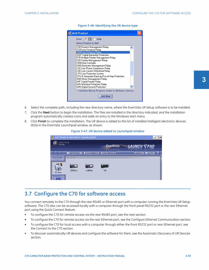
CHAPTER 3: INSTALLATION CONFIGURE THE C70 FOR SOFTWARE ACCESS
C70 CAPACITOR BANK PROTECTION AND CONTROL SYSTEM – INSTRUCTION MANUAL 3-39
3
Figure 3-46: Identifying the UR device type
6. Select the complete path, including the new directory name, where the EnerVista UR Setup software is to be installed.
7. Click the Next button to begin the installation. The files are installed in the directory indicated, and the installation program automatically creates icons and adds an entry to the Windows start menu.
8. Click Finish to complete the installation. The UR device is added to the list of installed intelligent electronic devices (IEDs) in the EnerVista Launchpad window, as shown.
Figure 3-47: UR device added to Launchpad window
3.7 Configure the C70 for software accessYou connect remotely to the C70 through the rear RS485 or Ethernet port with a computer running the EnerVista UR Setup software. The C70 also can be accessed locally with a computer through the front panel RS232 port or the rear Ethernet port using the Quick Connect feature.
• To configure the C70 for remote access via the rear RS485 port, see the next section.
• To configure the C70 for remote access via the rear Ethernet port, see the Configure Ethernet Communication section.
• To configure the C70 for local access with a computer through either the front RS232 port or rear Ethernet port, see the Connect to the C70 section.
• To discover automatically UR devices and configure the software for them, see the Automatic Discovery of UR Devices section.

3-40 C70 CAPACITOR BANK PROTECTION AND CONTROL SYSTEM – INSTRUCTION MANUAL
CONFIGURE THE C70 FOR SOFTWARE ACCESS CHAPTER 3: INSTALLATION
3
3.7.1 Configure serial communicationA computer with an RS232 port and a serial cable are required. To use the RS485 port at the back of the relay, a GE Digital Energy F485 converter (or compatible RS232-to-RS485 converter) is required. See the F485 instruction manual for details.
1. Connect the computer to the F485 and the F485 to the RS485 terminal on the back of the UR device, or connect directly the computer to the RS232 port on the front of the relay.
2. In the EnerVista Launchpad software on the computer, select the UR device to start the software.
3. Click the Device Setup button to open the Device Setup window, and click the Add Site button to define a new site.
4. Enter a site name in the Site Name field. Optionally add a short description of the site along with the display order of devices defined for the site. This example uses “Location 1” as the site name. When done, click the OK button. The new site appears in the upper-left list in the EnerVista UR Setup window.
5. Click the Device Setup button, then select the new site to re-open the Device Setup window.
6. Click the Add Device button to define the new device.
7. Enter a name in the Device Name field and a description (optional) of the site.
8. Select “Serial” from the Interface drop-down list. This displays a number of interface parameters that must be entered for serial communications.
Figure 3-48: Configuring serial communication
9. Enter the COM port used by the computer, the baud rate, and parity settings from the front panel SETTINGS PRODUCT SETUP COMMUNICATIONS SERIAL PORTS menu, and the relay slave address setting from the front panel SETTINGS PRODUCT SETUP COMMUNICATIONS MODBUS PROTOCOL MODBUS SLAVE ADDRESS menu in their respective fields.
10. Click the Read Order Code button to connect to the C70 and upload the order code to the software. If a communications error occurs, ensure that the EnerVista UR Setup serial communications values entered in the previous step correspond to the relay setting values.
11. Click the OK button when the relay order code has been received. The new device is added to the Site List window (or Online window) located in the top left corner of the main EnerVista UR Setup window.
The device has now been configured for RS232 communications. Proceed to the Connect to the C70 section to begin communication.
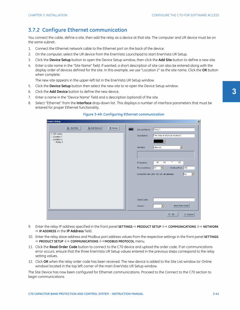
CHAPTER 3: INSTALLATION CONFIGURE THE C70 FOR SOFTWARE ACCESS
C70 CAPACITOR BANK PROTECTION AND CONTROL SYSTEM – INSTRUCTION MANUAL 3-41
3
3.7.2 Configure Ethernet communicationYou connect the cable, define a site, then add the relay as a device at that site. The computer and UR device must be on the same subnet.
1. Connect the Ethernet network cable to the Ethernet port on the back of the device.
2. On the computer, select the UR device from the EnerVista Launchpad to start EnerVista UR Setup.
3. Click the Device Setup button to open the Device Setup window, then click the Add Site button to define a new site.
4. Enter a site name in the “Site Name” field. If wanted, a short description of site can also be entered along with the display order of devices defined for the site. In this example, we use “Location 2” as the site name. Click the OK button when complete.
The new site appears in the upper-left list in the EnerVista UR Setup window.
5. Click the Device Setup button then select the new site to re-open the Device Setup window.
6. Click the Add Device button to define the new device.
7. Enter a name in the “Device Name” field and a description (optional) of the site.
8. Select “Ethernet” from the Interface drop-down list . This displays a number of interface parameters that must be entered for proper Ethernet functionality.
Figure 3-49: Configuring Ethernet communication
9. Enter the relay IP address specified in the front panel SETTINGS PRODUCT SETUP COMMUNICATIONS NETWORK IP ADDRESS in the IP Address field.
10. Enter the relay slave address and Modbus port address values from the respective settings in the front panel SETTINGS PRODUCT SETUP COMMUNICATIONS MODBUS PROTOCOL menu.
11. Click the Read Order Code button to connect to the C70 device and upload the order code. If an communications error occurs, ensure that the three EnerVista UR Setup values entered in the previous steps correspond to the relay setting values.
12. Click OK when the relay order code has been received. The new device is added to the Site List window (or Online window) located in the top left corner of the main EnerVista UR Setup window.
The Site Device has now been configured for Ethernet communications. Proceed to the Connect to the C70 section to begin communications.

3-42 C70 CAPACITOR BANK PROTECTION AND CONTROL SYSTEM – INSTRUCTION MANUAL
CONNECT TO THE C70 CHAPTER 3: INSTALLATION
3
3.7.3 Automatic discovery of UR devicesThe EnerVista UR Setup software can automatically discover and communicate to all UR-series IEDs located on an Ethernet network.
Using the Discover button in the Device Setup window, a single click of the mouse triggers the software to detect automatically any UR-series relays located on the network. The EnerVista UR Setup software then proceeds to configure all settings and order code options in the window. This feature allows the user to identify and interrogate all UR-series devices at a location.
To discover UR devices:
1. In EnerVista, click the Device Setup button.
2. In the window that opens, click the Discover button. If the required device is not found, add it manually as outlined earlier.
Figure 3-50: Discover button to detect UR devices in network
3.8 Connect to the C70There are four ways to the connect to the device, as follows:
• RS232 port (outlined here)
• RS485 port
• Ethernet port (outlined here)
• LAN
When unable to connect because of an "ACCESS VIOLATION," access Device Setup and refresh the order code for the device.
3.8.1 Connect to the C70 in EnerVistaFor information on using the EnerVista software, see the Interfaces chapter.
To access the relay in EnerVista:
1. Open the Settings > Product Setup > Display Properties window as shown. The window opens with a status indicator on the lower left of the EnerVista UR Setup window.

CHAPTER 3: INSTALLATION CONNECT TO THE C70
C70 CAPACITOR BANK PROTECTION AND CONTROL SYSTEM – INSTRUCTION MANUAL 3-43
3
Figure 3-51: EnerVista window
2. If the status indicator is red, verify that the Ethernet network cable is properly connected to the Ethernet port on the back of the relay and that the relay has been properly set up for communications (steps A and B earlier).
3. If a relay icon appears in place of the status indicator, then a report (such as an oscillography or event record) is open. Close the report to re-display the green status indicator.
4. The Display Properties settings can now be edited, printed, or changed.
3.8.1.1 Quick action hot linksThe EnerVista UR Setup software has several quick action buttons to provide instant access to several functions that are performed often when using URs. From the online window, users can select the relay to interrogate from a pull-down window, then click the button for the action to perform. The following quick action functions are available:
• View the event record
• View the last recorded oscillography record
• View the status of all C70 inputs and outputs
• View all of the C70 metering values
• View the C70 protection summary
• Generate a service report
3.8.2 Use Quick Connect via the front panel RS232 portTo connect to the UR from a computer using a serial cable:
1. Connect a nine-pin to nine-pin RS232 serial cable to the computer and the front panel RS232 port.
2. Verify that the latest version of the EnerVista UR Setup software is installed (available from the GE EnerVista DVD or online from http://www.gedigitalenergy.com/multilin). See the software installation section if not already installed.
3. Select the UR device from the EnerVista Launchpad to start EnerVista UR Setup.
4. Click the Quick Connect button to open the window.
842743A3.CDR
Communications status indicators:
Green = OK
Red = No communications
UR icon = report is open
Quick action hot links
Expand the site list by double-clicking
or selecting the +/– box.

3-44 C70 CAPACITOR BANK PROTECTION AND CONTROL SYSTEM – INSTRUCTION MANUAL
CONNECT TO THE C70 CHAPTER 3: INSTALLATION
3
Figure 3-52: Quick Connect window to access a device
5. Select the Serial interface and the correct COM Port, then click Connect .
6. The EnerVista UR Setup software creates a site named “Quick Connect” with a corresponding device also named “Quick Connect” and displays them on the left side of the screen. Expand the sections to view data directly from the C70 device. Use the Device Setup button to change the site names.
Each time that the EnerVista UR Setup software is initialized, click the Quick Connect button to establish direct communications to the C70. This ensures that configuration of the EnerVista UR Setup software matches the C70 model number.
3.8.3 Use Quick Connect via a rear Ethernet portTo use the Quick Connect feature to access the C70 from a computer through Ethernet, first assign an IP address to the relay using the front panel keyboard.
1. Press the MENU key until the Settings menu displays.
2. Navigate to Settings Product Setup Communications Network IP Address Setting.
3. Enter an IP address, for example “1.1.1.1,” and press the ENTER key to save the value.
4. In the same menu, select the Subnet IP Mask setting.
5. Enter a subnet IP address, for example “255.0.0.0,” and press the ENTER key to save the value.
Next, use an Ethernet cross-over cable to connect the computer to the rear Ethernet port. In case you need it , the following figure shows the pinout for an Ethernet cross-over cable.
Figure 3-53: Ethernet cross-over cable PIN layout
Now, assign the computer an IP address compatible with the relay’s IP address.
1. From the Windows desktop, right-click the My Network Places icon and select Properties to open the network
842799A1.CDR
END 1 END 2
Pin Wire color Diagram Pin Wire color Diagram
1 White/orange 1 White/green
2 Orange 2 Green
3 White/green 3 White/orange
4 Blue 4 Blue
5 White/blue 5 White/blue
6 Green 6 Orange
7 White/brown 7 White/brown
8 Brown 8 Brown
1
2
34 5
6
7
8

CHAPTER 3: INSTALLATION CONNECT TO THE C70
C70 CAPACITOR BANK PROTECTION AND CONTROL SYSTEM – INSTRUCTION MANUAL 3-45
3
connections window.
2. Right-click the Local Area Connection icon and select Properties.
3. Select the Internet Protocol (TCP/IP) item from the list, and click the Properties button.

3-46 C70 CAPACITOR BANK PROTECTION AND CONTROL SYSTEM – INSTRUCTION MANUAL
CONNECT TO THE C70 CHAPTER 3: INSTALLATION
3
4. Click the “Use the following IP address” box.
5. Enter an IP address with the first three numbers the same as the IP address of the C70 relay and the last number different (in this example, 1.1.1.2).
6. Enter a subnet mask equal to the one set in the C70 (in this example, 255.0.0.0).
7. Click the OK button to save the values.
Before continuing, test the Ethernet connection.
1. Open a Windows console window, for example by selecting Start > Run from the Windows Start menu and typing “cmd” or clicking the Start button and entering "cmd".
2. Type the following command, substituting the IP address of 1.1.1.1 with yours:C:\WINNT>ping 1.1.1.1
3. If the connection is successful, the system returns four replies similar to the following:Pinging 1.1.1.1 with 32 bytes of data:
Reply from 1.1.1.1: bytes=32 time<10ms TTL=255
Reply from 1.1.1.1: bytes=32 time<10ms TTL=255Reply from 1.1.1.1: bytes=32 time<10ms TTL=255
Reply from 1.1.1.1: bytes=32 time<10ms TTL=255
Ping statistics for 1.1.1.1:Packets: Sent = 4, Received = 4, Lost = 0 (0% loss),
Approximate round trip time in milliseconds:
Minimum = 0ms, Maximum = 0ms, Average = 0 ms
4. Note that the values for time and TTL vary depending on local network configuration.
5. If the following sequence of messages appears when entering the C:\WINNT>ping 1.1.1.1 command:Pinging 1.1.1.1 with 32 bytes of data:
Request timed out.Request timed out.
Request timed out.
Request timed out.Ping statistics for 1.1.1.1:
Packets: Sent = 4, Received = 0, Lost = 4 (100% loss),
Approximate round trip time in milliseconds:Minimum = 0ms, Maximum = 0ms, Average = 0 ms
Pinging 1.1.1.1 with 32 bytes of data:
verify the physical connection between the C70 and the computer, and double-check the programmed IP address in the Product Setup Communications Network IP Address setting, then repeat step 2.
6. If the following sequence of messages appears when entering the C:\WINNT>ping 1.1.1.1 command:Pinging 1.1.1.1 with 32 bytes of data:Hardware error.
Hardware error.
Hardware error.Hardware error.
Ping statistics for 1.1.1.1:
Packets: Sent = 4, Received = 0, Lost = 4 (100% loss),Approximate round trip time in milliseconds:
Minimum = 0ms, Maximum = 0ms, Average = 0 ms
Pinging 1.1.1.1 with 32 bytes of data:
verify the physical connection between the C70 and the computer, and double-check the programmed IP address in the PRODUCT SETUP COMMUNICATIONS NETWORK IP ADDRESS setting, then repeat step 2.
7. If the following sequence of messages appears when entering the C:\WINNT>ping 1.1.1.1 command:Pinging 1.1.1.1 with 32 bytes of data:
Destination host unreachable.
Destination host unreachable.Destination host unreachable.
Destination host unreachable.
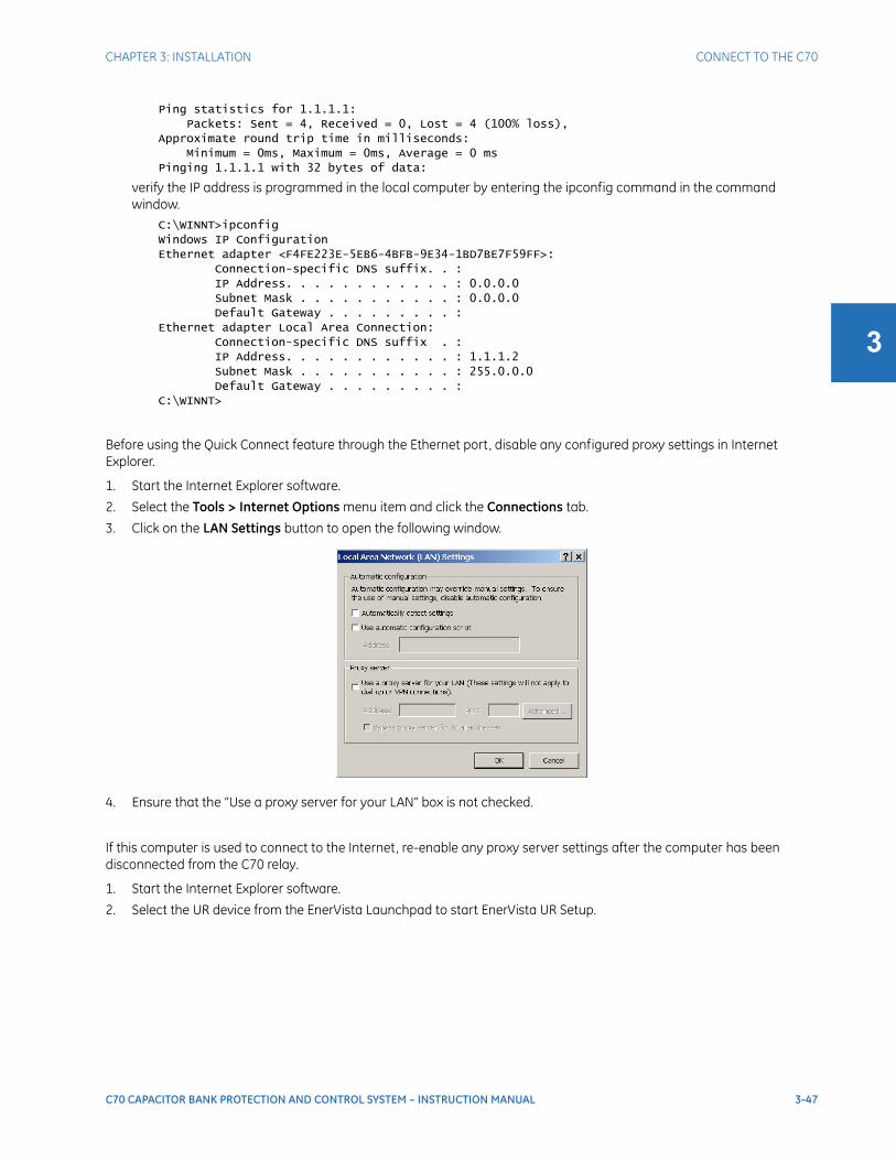
CHAPTER 3: INSTALLATION CONNECT TO THE C70
C70 CAPACITOR BANK PROTECTION AND CONTROL SYSTEM – INSTRUCTION MANUAL 3-47
3
Ping statistics for 1.1.1.1:Packets: Sent = 4, Received = 0, Lost = 4 (100% loss),
Approximate round trip time in milliseconds:
Minimum = 0ms, Maximum = 0ms, Average = 0 msPinging 1.1.1.1 with 32 bytes of data:
verify the IP address is programmed in the local computer by entering the ipconfig command in the command window.
C:\WINNT>ipconfig
Windows IP Configuration
Ethernet adapter <F4FE223E-5EB6-4BFB-9E34-1BD7BE7F59FF>:Connection-specific DNS suffix. . :
IP Address. . . . . . . . . . . . : 0.0.0.0
Subnet Mask . . . . . . . . . . . : 0.0.0.0Default Gateway . . . . . . . . . :
Ethernet adapter Local Area Connection:
Connection-specific DNS suffix . :IP Address. . . . . . . . . . . . : 1.1.1.2
Subnet Mask . . . . . . . . . . . : 255.0.0.0
Default Gateway . . . . . . . . . :C:\WINNT>
Before using the Quick Connect feature through the Ethernet port, disable any configured proxy settings in Internet Explorer.
1. Start the Internet Explorer software.
2. Select the Tools > Internet Options menu item and click the Connections tab.
3. Click on the LAN Settings button to open the following window.
4. Ensure that the “Use a proxy server for your LAN” box is not checked.
If this computer is used to connect to the Internet, re-enable any proxy server settings after the computer has been disconnected from the C70 relay.
1. Start the Internet Explorer software.
2. Select the UR device from the EnerVista Launchpad to start EnerVista UR Setup.

3-48 C70 CAPACITOR BANK PROTECTION AND CONTROL SYSTEM – INSTRUCTION MANUAL
CONNECT TO THE C70 CHAPTER 3: INSTALLATION
3
3. Click the Quick Connect button to open the window.
4. Select the Ethernet interface and enter the IP address assigned to the C70, then click the Connect button. The EnerVista UR Setup software creates a site named “Quick Connect” with a corresponding device also named “Quick Connect” and displays them on the left side of the screen.
5. Expand the sections to view data directly from the C70 device.
Each time that the EnerVista UR Setup software is initialized, click the Quick Connect button to establish direct communications to the C70. This ensures that configuration of the EnerVista UR Setup software matches the C70 model number.
When direct communications with the C70 via Ethernet is complete, make the following changes:
1. From the Windows desktop, right-click the My Network Places icon and select Properties to open the network connections window.
2. Right-click the Local Area Connection icon and select the Properties item.
3. Select the Internet Protocol (TCP/IP) item from the list provided and click the Properties button.
4. Set the computer to “Obtain a relay address automatically” as shown.
If the computer is used to connect to the Internet, re-enable any proxy server settings after the computer has been disconnected from the C70 relay.

CHAPTER 3: INSTALLATION SET UP CYBERSENTRY AND CHANGE DEFAULT PASSWORD
C70 CAPACITOR BANK PROTECTION AND CONTROL SYSTEM – INSTRUCTION MANUAL 3-49
3
3.9 Set up CyberSentry and change default passwordIf and when first using CyberSentry security, use the following procedure for set up.
1. Log in to the relay as Administrator by using the VALUE keys on the front panel or through EnerVista connected serially (so that no IP address is required). If logging in through EnerVista choose Device authentication. Enter the default password "ChangeMe1#". Note that the "Lock relay" setting needs to be disabled in the Security > Supervisory menu. When this setting is disabled, configuration and firmware upgrade are possible. By default, this setting is disabled.
2. Enable the Supervisor role if you have a need for it .
3. Make any required changes in configuration, such as setting a valid IP address for communication over Ethernet.
4. Log out of the Administrator account by choosing None.
Next, device or server authentication can be chosen on the login screen, but the choice is available only in EnerVista. Use device authentication to log in using the five pre-configured roles (Administrator, Supervisor, Engineer, Operator, Observer). When using a serial connection, only Device authentication is supported. When Server authentication is required, characteristics for communication with a RADIUS server must be configured on the UR. This is possible only through the EnerVista software. The RADIUS server itself also must be configured. At the end of this instruction manual, the appendix called RADIUS Server gives an example of how to setup a simple RADIUS server. Once both the RADIUS server and the parameters for connecting UR to the server have been configured, you can choose Server authentication on the login screen of EnerVista.
Figure 3-54: Login screen for CyberSentry
During the commissioning phase, you have the option to bypass the use of passwords. Do so by enabling the Bypass Access setting under Settings > Product Setup > Security > Supervisory. Be sure to disable this bypass setting after commissioning the device.
You can change the password for any role either from the front panel or through EnerVista.
If using EnerVista, navigate to Settings > Product Setup > Security. Change the Local Administrator Password, for example. It is strongly recommended that the password for the Administrator be changed from the default. Changing the passwords for the other three roles is optional.

3-50 C70 CAPACITOR BANK PROTECTION AND CONTROL SYSTEM – INSTRUCTION MANUAL
SET UP CYBERSENTRY AND CHANGE DEFAULT PASSWORD CHAPTER 3: INSTALLATION
3
Figure 3-55: Changing the default password
C70 CAPACITOR BANK PROTECTION AND CONTROL SYSTEM – INSTRUCTION MANUAL 4-1
C70 Capacitor Bank Protection and Control System
Chapter 4: Interfaces
Interfaces
This chapter explains the EnerVista software interface, the front panel interface, and logic diagrams.
4.1 EnerVista software interface
4.1.1 IntroductionThe EnerVista UR Setup software provides a single facility to configure, monitor, maintain, and troubleshoot relay functions, connected over local or wide area communication networks. It can be used while disconnected (offline) or connected (online) to a UR device. In offline mode, settings files can be created for eventual downloading to the device. In online mode, you communicate with the device in real-time.
The EnerVista UR Setup software is provided with every C70. This chapter outlines the EnerVista software interface features. The EnerVista UR Setup Help File also provides details for getting started and using the software interface.
4.1.2 Settings filesThe EnerVista software supports the following three ways of handling changes to relay settings:
• In offline mode (relay disconnected) to create or edit relay settings files for later download to relays
• While connected to a communicating relay to modify directly any relay settings via relay data view windows, and then save the settings to the relay
• Create/edit settings files and then write them to the relay while connected to the relay
Settings files are organized on the basis of file names assigned by the user. A settings file contains data pertaining to the following types of relay settings:
• Device definition
• Product setup
• System setup
• FlexLogic
• Grouped elements
• Control elements
• Inputs/outputs
• Remote resources
4-2 C70 CAPACITOR BANK PROTECTION AND CONTROL SYSTEM – INSTRUCTION MANUAL
ENERVISTA SOFTWARE INTERFACE CHAPTER 4: INTERFACES
4
• Testing
Factory default values are supplied and can be restored after any changes.
The following communications settings are not transferred to the C70 with settings files:Modbus Slave AddressModbus TCP Port NumberRS485 COM2 Baud RateRS485 COM2 ParityCOM2 Minimum Response TimeCOM2 SelectionRRTD Slave AddressRRTD Baud RateIP AddressIP Subnet MaskIP Routing
When a settings file is loaded to a C70 that is in-service, the following sequence occurs:
1. The C70 takes itself out of service.
2. The C70 issues a UNIT NOT PROGRAMMED major self-test error.
3. The C70 closes the critical fail contact.
The Maintenance chapter outlines how to use a settings file in the .urs format for backup and restore.
4.1.3 Event viewingWhile the interface is in either online or offline mode, you can view and analyze data generated by triggered parameters, via one of the following:
• Event recorder — The event recorder captures contextual data associated with the last 1024 events, listed in chronological order from most recent to oldest
• Oscillography — The oscillography waveform traces and digital states are used to provide a visual display of power system and relay operation data captured during specific triggered events
4.1.4 File supportThe following support applies, where the Settings List is at the bottom left and the Site List is at the top left of the EnerVista window:
• Execution — Any EnerVista UR Setup file that is opened launches the application or provides focus to the already opened application. If the file was a settings file (has a .urs extension) that had been removed from the Settings List navigation menu, it is added back to the menu.
• Drag and Drop — The Site List and Settings List control bar windows are each mutually a drag source and a drop target for device-order-code-compatible files or individual menu items. Also, the Settings List control bar window and any Windows Explorer directory folder are each mutually a file drag source and drop target.
New files that are dropped into the Settings List window are added to the tree, which is automatically sorted alphabetically with respect to settings file names. Files or individual menu items that are dropped in the selected device menu in the Site List window are automatically sent to the online communicating device.
4.1.5 EnerVista main windowThe EnerVista UR Setup software window has the following components:
1. Title bar that shows the pathname of the active data view or the name of the software
2. Main window menu bar
3. Main window tool bar
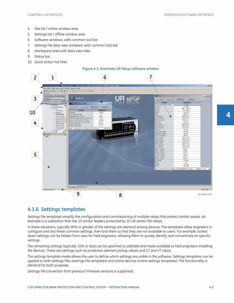
CHAPTER 4: INTERFACES ENERVISTA SOFTWARE INTERFACE
C70 CAPACITOR BANK PROTECTION AND CONTROL SYSTEM – INSTRUCTION MANUAL 4-3
4
4. Site list / online window area
5. Settings list / offline window area
6. Software windows, with common tool bar
7. Settings file data view windows, with common tool bar
8. Workspace area with data view tabs
9. Status bar
10. Quick action hot links
Figure 4-1: EnerVista UR Setup software window
4.1.6 Settings templatesSettings file templates simplify the configuration and commissioning of multiple relays that protect similar assets. An example is a substation that has 10 similar feeders protected by 10 UR-series F60 relays.
In these situations, typically 90% or greater of the settings are identical among devices. The templates allow engineers to configure and test these common settings, then lock them so that they are not available to users. For example, locked down settings can be hidden from view for field engineers, allowing them to quickly identify and concentrate on specific settings.
The remaining settings (typically 10% or less) can be specified as editable and made available to field engineers installing the devices. These are settings such as protection element pickup values and CT and VT ratios.
The settings template mode allows the user to define which settings are visible in the software. Settings templates can be applied to both settings files (settings file templates) and online devices (online settings templates). The functionality is identical for both purposes.
Settings file conversion from previous firmware versions is supported.
12
3
4
5
6 7
89 842786A2.CDR
10
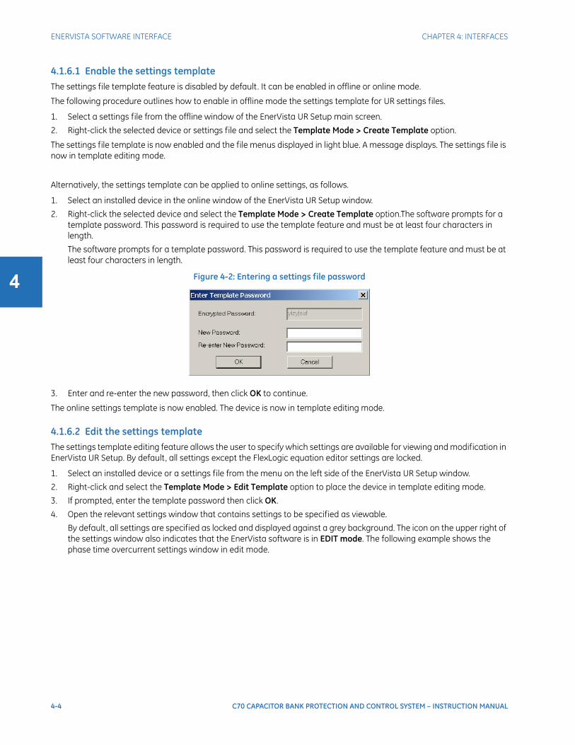
4-4 C70 CAPACITOR BANK PROTECTION AND CONTROL SYSTEM – INSTRUCTION MANUAL
ENERVISTA SOFTWARE INTERFACE CHAPTER 4: INTERFACES
4
4.1.6.1 Enable the settings templateThe settings file template feature is disabled by default. It can be enabled in offline or online mode.
The following procedure outlines how to enable in offline mode the settings template for UR settings files.
1. Select a settings file from the offline window of the EnerVista UR Setup main screen.
2. Right-click the selected device or settings file and select the Template Mode > Create Template option.
The settings file template is now enabled and the file menus displayed in light blue. A message displays. The settings file is now in template editing mode.
Alternatively, the settings template can be applied to online settings, as follows.
1. Select an installed device in the online window of the EnerVista UR Setup window.
2. Right-click the selected device and select the Template Mode > Create Template option.The software prompts for a template password. This password is required to use the template feature and must be at least four characters in length.
The software prompts for a template password. This password is required to use the template feature and must be at least four characters in length.
Figure 4-2: Entering a settings file password
3. Enter and re-enter the new password, then click OK to continue.
The online settings template is now enabled. The device is now in template editing mode.
4.1.6.2 Edit the settings templateThe settings template editing feature allows the user to specify which settings are available for viewing and modification in EnerVista UR Setup. By default, all settings except the FlexLogic equation editor settings are locked.
1. Select an installed device or a settings file from the menu on the left side of the EnerVista UR Setup window.
2. Right-click and select the Template Mode > Edit Template option to place the device in template editing mode.
3. If prompted, enter the template password then click OK.
4. Open the relevant settings window that contains settings to be specified as viewable.
By default, all settings are specified as locked and displayed against a grey background. The icon on the upper right of the settings window also indicates that the EnerVista software is in EDIT mode. The following example shows the phase time overcurrent settings window in edit mode.

CHAPTER 4: INTERFACES ENERVISTA SOFTWARE INTERFACE
C70 CAPACITOR BANK PROTECTION AND CONTROL SYSTEM – INSTRUCTION MANUAL 4-5
4
Figure 4-3: Settings template with all settings specified as locked
5. Specify the settings to make viewable by clicking them.
A setting available to view is displayed against a yellow background.
Figure 4-4: Settings template with two settings specified as editable
6. Click the Save button to save changes to the settings template.
7. Continue through any other settings window to specify all viewable settings.
4.1.6.3 Add password protection to a templateIt is highly recommended that templates be saved with password protection to maximize security.
The following procedure outlines how to add password protection to a settings file template.
1. Select a settings file from the offline window on the left of the EnerVista UR Setup window.
2. Select the Template Mode > Password Protect Template option.
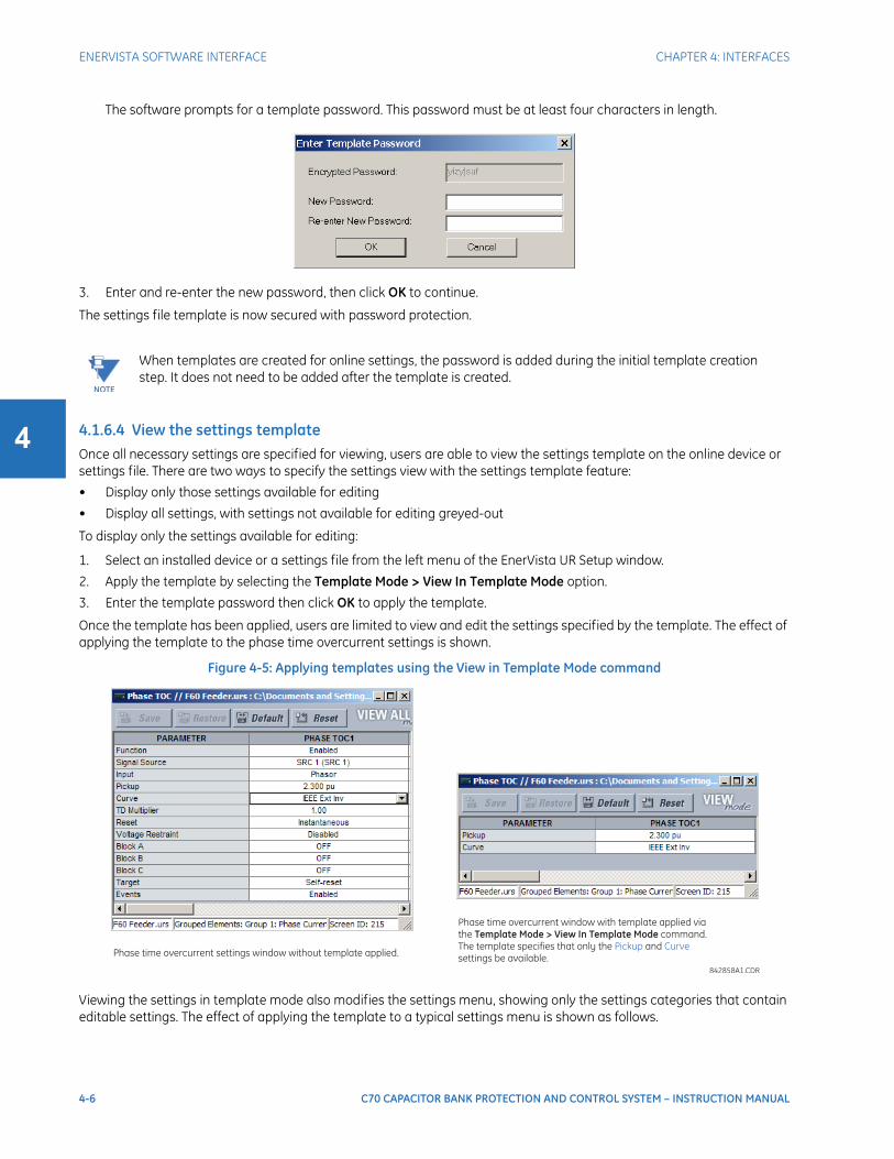
4-6 C70 CAPACITOR BANK PROTECTION AND CONTROL SYSTEM – INSTRUCTION MANUAL
ENERVISTA SOFTWARE INTERFACE CHAPTER 4: INTERFACES
4
The software prompts for a template password. This password must be at least four characters in length.
3. Enter and re-enter the new password, then click OK to continue.
The settings file template is now secured with password protection.
4.1.6.4 View the settings templateOnce all necessary settings are specified for viewing, users are able to view the settings template on the online device or settings file. There are two ways to specify the settings view with the settings template feature:
• Display only those settings available for editing
• Display all settings, with settings not available for editing greyed-out
To display only the settings available for editing:
1. Select an installed device or a settings file from the left menu of the EnerVista UR Setup window.
2. Apply the template by selecting the Template Mode > View In Template Mode option.
3. Enter the template password then click OK to apply the template.
Once the template has been applied, users are limited to view and edit the settings specified by the template. The effect of applying the template to the phase time overcurrent settings is shown.
Figure 4-5: Applying templates using the View in Template Mode command
Viewing the settings in template mode also modifies the settings menu, showing only the settings categories that contain editable settings. The effect of applying the template to a typical settings menu is shown as follows.
NOTE
When templates are created for online settings, the password is added during the initial template creation step. It does not need to be added after the template is created.
Phase time overcurrent settings window without template applied.
Phase time overcurrent window with template applied via
the command.
The template specifies that only the and
settings be available.
Template Mode > View In Template Mode
Pickup Curve
842858A1.CDR
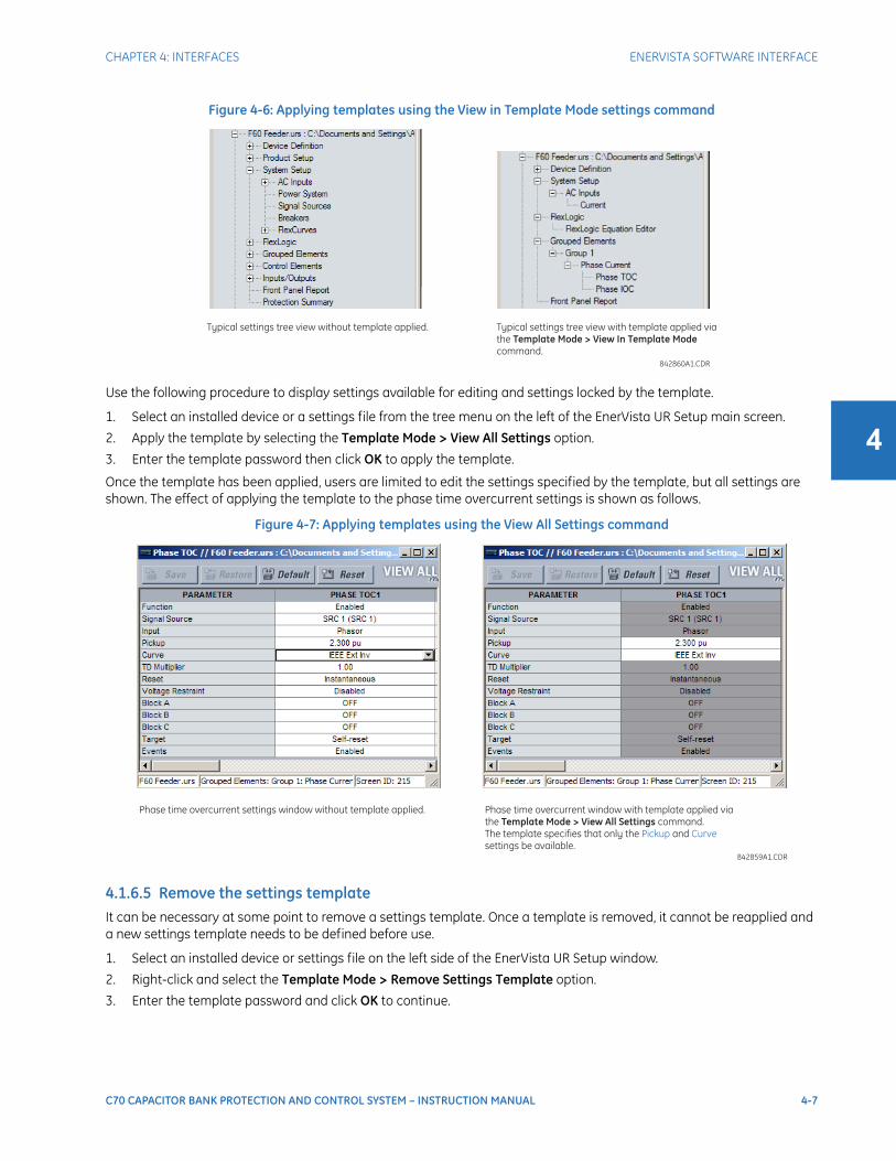
CHAPTER 4: INTERFACES ENERVISTA SOFTWARE INTERFACE
C70 CAPACITOR BANK PROTECTION AND CONTROL SYSTEM – INSTRUCTION MANUAL 4-7
4
Figure 4-6: Applying templates using the View in Template Mode settings command
Use the following procedure to display settings available for editing and settings locked by the template.
1. Select an installed device or a settings file from the tree menu on the left of the EnerVista UR Setup main screen.
2. Apply the template by selecting the Template Mode > View All Settings option.
3. Enter the template password then click OK to apply the template.
Once the template has been applied, users are limited to edit the settings specified by the template, but all settings are shown. The effect of applying the template to the phase time overcurrent settings is shown as follows.
Figure 4-7: Applying templates using the View All Settings command
4.1.6.5 Remove the settings templateIt can be necessary at some point to remove a settings template. Once a template is removed, it cannot be reapplied and a new settings template needs to be defined before use.
1. Select an installed device or settings file on the left side of the EnerVista UR Setup window.
2. Right-click and select the Template Mode > Remove Settings Template option.
3. Enter the template password and click OK to continue.
Typical settings tree view without template applied. Typical settings tree view with template applied via
the
command.
Template Mode > View In Template Mode
842860A1.CDR
Phase time overcurrent settings window without template applied. Phase time overcurrent window with template applied via
the command.
The template specifies that only the and
settings be available.
Template Mode > View All Settings
Pickup Curve
842859A1.CDR
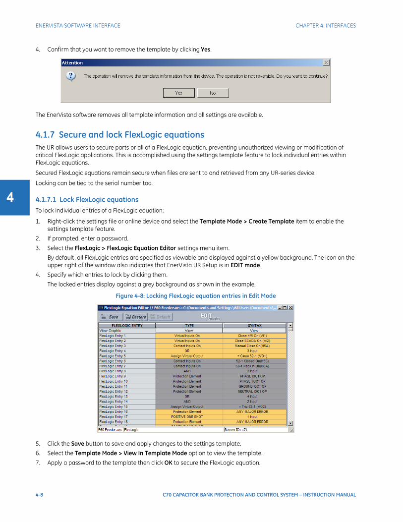
4-8 C70 CAPACITOR BANK PROTECTION AND CONTROL SYSTEM – INSTRUCTION MANUAL
ENERVISTA SOFTWARE INTERFACE CHAPTER 4: INTERFACES
4
4. Confirm that you want to remove the template by clicking Yes.
The EnerVista software removes all template information and all settings are available.
4.1.7 Secure and lock FlexLogic equationsThe UR allows users to secure parts or all of a FlexLogic equation, preventing unauthorized viewing or modification of critical FlexLogic applications. This is accomplished using the settings template feature to lock individual entries within FlexLogic equations.
Secured FlexLogic equations remain secure when files are sent to and retrieved from any UR-series device.
Locking can be tied to the serial number too.
4.1.7.1 Lock FlexLogic equationsTo lock individual entries of a FlexLogic equation:
1. Right-click the settings file or online device and select the Template Mode > Create Template item to enable the settings template feature.
2. If prompted, enter a password.
3. Select the FlexLogic > FlexLogic Equation Editor settings menu item.
By default, all FlexLogic entries are specified as viewable and displayed against a yellow background. The icon on the upper right of the window also indicates that EnerVista UR Setup is in EDIT mode.
4. Specify which entries to lock by clicking them.
The locked entries display against a grey background as shown in the example.
Figure 4-8: Locking FlexLogic equation entries in Edit Mode
5. Click the Save button to save and apply changes to the settings template.
6. Select the Template Mode > View In Template Mode option to view the template.
7. Apply a password to the template then click OK to secure the FlexLogic equation.

CHAPTER 4: INTERFACES ENERVISTA SOFTWARE INTERFACE
C70 CAPACITOR BANK PROTECTION AND CONTROL SYSTEM – INSTRUCTION MANUAL 4-9
4
Once the template has been applied, users are limited to view and edit the FlexLogic entries not locked by the template. The effect of applying the template to the FlexLogic entries is shown here.
Figure 4-9: Locking FlexLogic entries through settings templates
The FlexLogic entries are also shown as locked in the graphical view and on the front panel display.
Figure 4-10: Secured FlexLogic in graphical view
4.1.7.2 Lock FlexLogic equations to the serial numberA settings file and associated FlexLogic equations also can be locked to a UR serial number. Once FlexLogic entries in a settings file have been secured, use the following procedure to lock the settings file to a serial number.
1. Right-click the setting file in the offline window area and select the Edit Settings File Properties item. The window opens.
Typical FlexLogic™ entries without template applied. Typical locked with template via
the command.Template Mode > View In Template Mode
FlexLogic™ entries
842861A1.CDR

4-10 C70 CAPACITOR BANK PROTECTION AND CONTROL SYSTEM – INSTRUCTION MANUAL
ENERVISTA SOFTWARE INTERFACE CHAPTER 4: INTERFACES
4
Figure 4-11: Settings file properties window
2. Enter the serial number of the C70 device to lock to the settings file in the Serial # Lock field.
3. Click the OK button to apply the change.
The settings file and corresponding secure FlexLogic equations are now locked to the C70 device specified by the serial number.
4.1.8 Settings file traceabilityA traceability feature for settings files allows the user to quickly determine if the settings in a C70 device have been changed since the time of installation from a settings file. When a settings file is transferred to a C70 device, the date, time, and serial number of the C70 are sent back to EnerVista UR Setup and added to the settings file on the local computer. This information can be compared with the C70 actual values at any later date to determine if security has been compromised.
The traceability information is only included in the settings file if a complete settings file is either transferred to the C70 device or obtained from the C70 device. Any partial settings transfers by way of drag and drop do not add the traceability information to the settings file.
Figure 4-12: Settings file traceability

CHAPTER 4: INTERFACES ENERVISTA SOFTWARE INTERFACE
C70 CAPACITOR BANK PROTECTION AND CONTROL SYSTEM – INSTRUCTION MANUAL 4-11
4
With respect to the figure, the traceability feature is used as follows.
1. The transfer date of a settings file written to a C70 is logged in the relay and can be viewed in the EnerVista software or the front panel display. Likewise, the transfer date of a settings file saved to a local computer is logged in the EnerVista software.
2. Comparing the dates stored in the relay and on the settings file at any time in the future indicates if any changes have been made to the relay configuration since the settings file was saved.
4.1.8.1 Settings file traceability informationThe serial number and file transfer date are saved in the settings files when they are sent to a C70 device.
The C70 serial number and file transfer date are included in the settings file device definition within the EnerVista UR Setup offline window as shown in the example.
Figure 4-13: Device definition showing traceability data
This information is also available in printed settings file reports as shown in the example.
Figure 4-14: Settings file report showing traceability data
4.1.8.2 Online device traceability informationThe C70 serial number and file transfer date are available for an online device through the actual values. Select the Actual Values > Product Info > Model Information menu item within the EnerVista online window as shown in the example.
Traceability data in settings
file device definition
842863A1.CDR
Traceability data
in settings report
842862A1.CDR
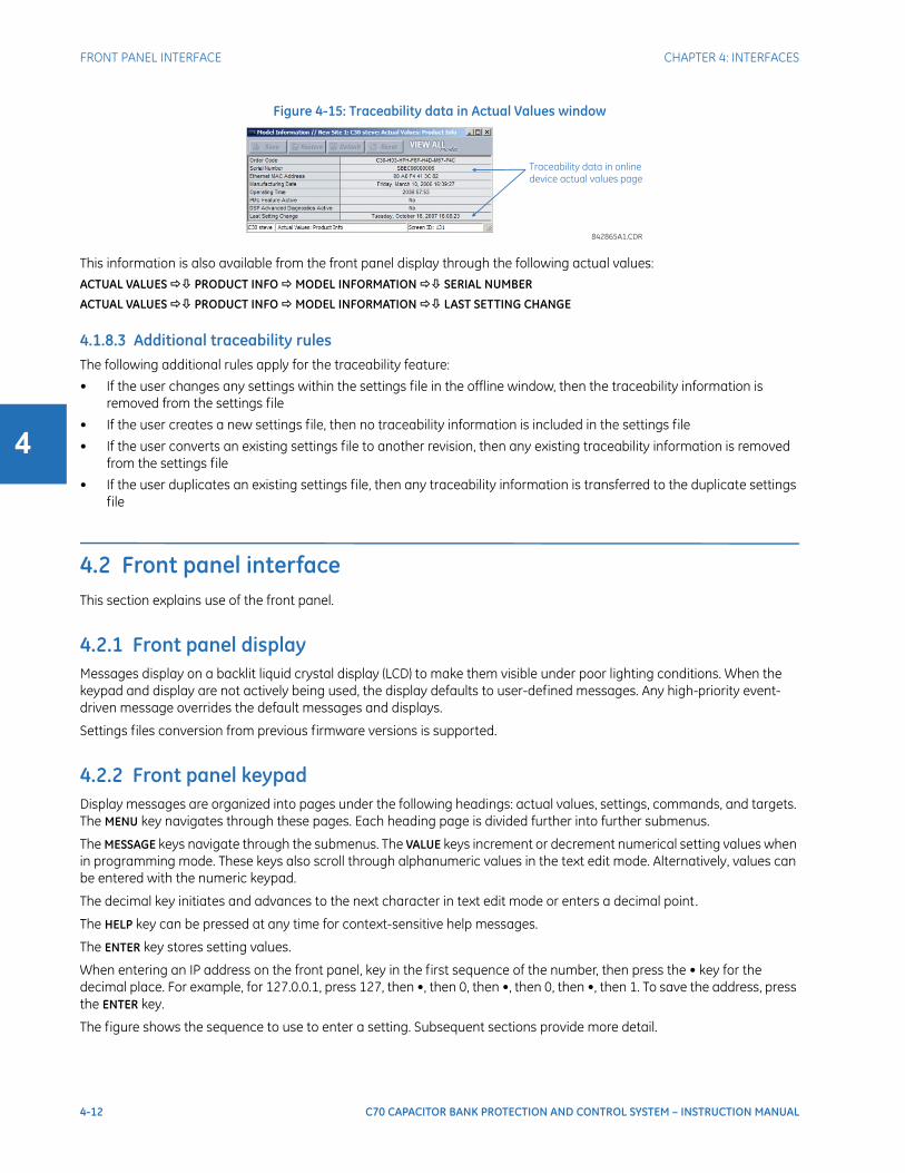
4-12 C70 CAPACITOR BANK PROTECTION AND CONTROL SYSTEM – INSTRUCTION MANUAL
FRONT PANEL INTERFACE CHAPTER 4: INTERFACES
4
Figure 4-15: Traceability data in Actual Values window
This information is also available from the front panel display through the following actual values:
ACTUAL VALUES PRODUCT INFO MODEL INFORMATION SERIAL NUMBER
ACTUAL VALUES PRODUCT INFO MODEL INFORMATION LAST SETTING CHANGE
4.1.8.3 Additional traceability rulesThe following additional rules apply for the traceability feature:
• If the user changes any settings within the settings file in the offline window, then the traceability information is removed from the settings file
• If the user creates a new settings file, then no traceability information is included in the settings file
• If the user converts an existing settings file to another revision, then any existing traceability information is removed from the settings file
• If the user duplicates an existing settings file, then any traceability information is transferred to the duplicate settings file
4.2 Front panel interfaceThis section explains use of the front panel.
4.2.1 Front panel displayMessages display on a backlit liquid crystal display (LCD) to make them visible under poor lighting conditions. When the keypad and display are not actively being used, the display defaults to user-defined messages. Any high-priority event-driven message overrides the default messages and displays.
Settings files conversion from previous firmware versions is supported.
4.2.2 Front panel keypadDisplay messages are organized into pages under the following headings: actual values, settings, commands, and targets. The MENU key navigates through these pages. Each heading page is divided further into further submenus.
The MESSAGE keys navigate through the submenus. The VALUE keys increment or decrement numerical setting values when in programming mode. These keys also scroll through alphanumeric values in the text edit mode. Alternatively, values can be entered with the numeric keypad.
The decimal key initiates and advances to the next character in text edit mode or enters a decimal point.
The HELP key can be pressed at any time for context-sensitive help messages.
The ENTER key stores setting values.
When entering an IP address on the front panel, key in the first sequence of the number, then press the • key for the decimal place. For example, for 127.0.0.1, press 127, then •, then 0, then •, then 0, then •, then 1. To save the address, press the ENTER key.
The figure shows the sequence to use to enter a setting. Subsequent sections provide more detail.
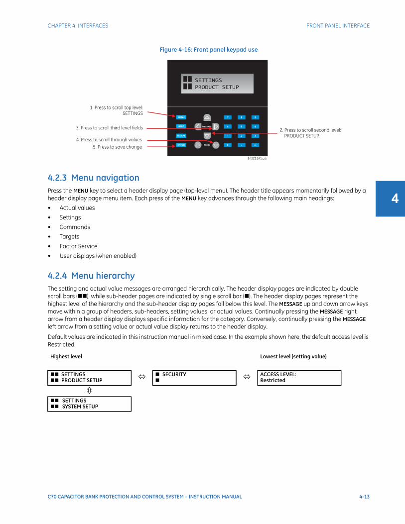
CHAPTER 4: INTERFACES FRONT PANEL INTERFACE
C70 CAPACITOR BANK PROTECTION AND CONTROL SYSTEM – INSTRUCTION MANUAL 4-13
4
Figure 4-16: Front panel keypad use
4.2.3 Menu navigationPress the MENU key to select a header display page (top-level menu). The header title appears momentarily followed by a header display page menu item. Each press of the MENU key advances through the following main headings:
• Actual values
• Settings
• Commands
• Targets
• Factor Service
• User displays (when enabled)
4.2.4 Menu hierarchyThe setting and actual value messages are arranged hierarchically. The header display pages are indicated by double scroll bars (), while sub-header pages are indicated by single scroll bar (). The header display pages represent the highest level of the hierarchy and the sub-header display pages fall below this level. The MESSAGE up and down arrow keys move within a group of headers, sub-headers, setting values, or actual values. Continually pressing the MESSAGE right arrow from a header display displays specific information for the category. Conversely, continually pressing the MESSAGE left arrow from a setting value or actual value display returns to the header display.
Default values are indicated in this instruction manual in mixed case. In the example shown here, the default access level is Restricted.
Highest level Lowest level (setting value)
SETTINGS PRODUCT SETUP SECURITY
ACCESS LEVEL:Restricted
SETTINGS SYSTEM SETUP
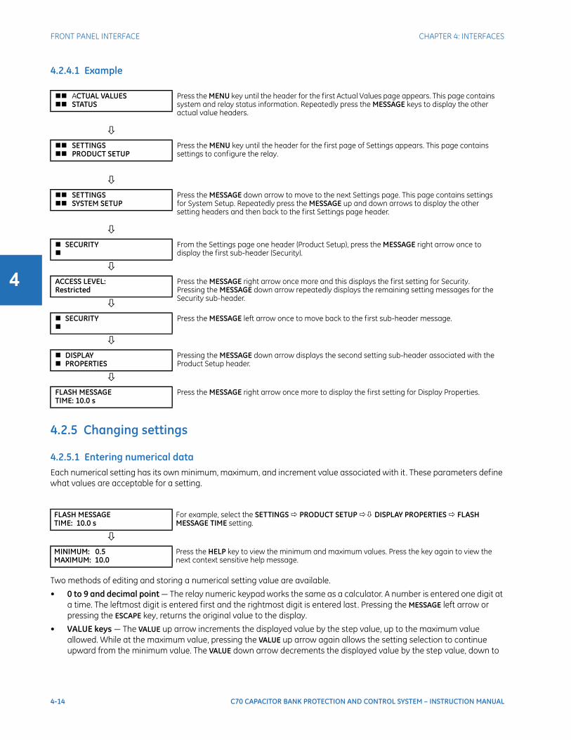
4-14 C70 CAPACITOR BANK PROTECTION AND CONTROL SYSTEM – INSTRUCTION MANUAL
FRONT PANEL INTERFACE CHAPTER 4: INTERFACES
4
4.2.4.1 Example
4.2.5 Changing settings
4.2.5.1 Entering numerical dataEach numerical setting has its own minimum, maximum, and increment value associated with it . These parameters define what values are acceptable for a setting.
Two methods of editing and storing a numerical setting value are available.
• 0 to 9 and decimal point — The relay numeric keypad works the same as a calculator. A number is entered one digit at a time. The leftmost digit is entered first and the rightmost digit is entered last. Pressing the MESSAGE left arrow or pressing the ESCAPE key, returns the original value to the display.
• VALUE keys — The VALUE up arrow increments the displayed value by the step value, up to the maximum value allowed. While at the maximum value, pressing the VALUE up arrow again allows the setting selection to continue upward from the minimum value. The VALUE down arrow decrements the displayed value by the step value, down to
ACTUAL VALUES STATUS
Press the MENU key until the header for the first Actual Values page appears. This page contains system and relay status information. Repeatedly press the MESSAGE keys to display the other actual value headers.
SETTINGS PRODUCT SETUP
Press the MENU key until the header for the first page of Settings appears. This page contains settings to configure the relay.
SETTINGS SYSTEM SETUP
Press the MESSAGE down arrow to move to the next Settings page. This page contains settings for System Setup. Repeatedly press the MESSAGE up and down arrows to display the other setting headers and then back to the first Settings page header.
SECURITY
From the Settings page one header (Product Setup), press the MESSAGE right arrow once to display the first sub-header (Security).
ACCESS LEVEL:Restricted
Press the MESSAGE right arrow once more and this displays the first setting for Security. Pressing the MESSAGE down arrow repeatedly displays the remaining setting messages for the Security sub-header.
SECURITY
Press the MESSAGE left arrow once to move back to the first sub-header message.
DISPLAY PROPERTIES
Pressing the MESSAGE down arrow displays the second setting sub-header associated with the Product Setup header.
FLASH MESSAGETIME: 10.0 s
Press the MESSAGE right arrow once more to display the first setting for Display Properties.
FLASH MESSAGETIME: 10.0 s
For example, select the SETTINGS PRODUCT SETUP DISPLAY PROPERTIES FLASH MESSAGE TIME setting.
MINIMUM: 0.5MAXIMUM: 10.0
Press the HELP key to view the minimum and maximum values. Press the key again to view the next context sensitive help message.

CHAPTER 4: INTERFACES FRONT PANEL INTERFACE
C70 CAPACITOR BANK PROTECTION AND CONTROL SYSTEM – INSTRUCTION MANUAL 4-15
4
the minimum value. While at the minimum value, pressing the VALUE down arrow again allows the setting selection to continue downward from the maximum value.
4.2.5.2 Entering enumeration dataEnumeration settings have data values that are part of a set, whose members are explicitly defined by a name. A set has two or more members.
Enumeration type values are changed using the VALUE keys. The VALUE up arrow displays the next selection while the VALUE down arrow displays the previous selection.
4.2.5.3 Entering alphanumeric textText settings have data values that are fixed in length, but user-defined in characters. They can be upper-case letters, lower-case letters, numerals, and a selection of special characters.
There are several places where text messages can be programmed to allow the relay to be customized for specific applications. One example is the Message Scratchpad. Use the following procedure to enter alphanumeric text messages.
For example, enter the text “Breaker #1”.
1. Press the decimal point to enter text edit mode.
2. Press the VALUE keys until the character 'B' appears; press the decimal key to advance the cursor to the next position.
3. Repeat step 2 for the remaining characters: r,e,a,k,e,r, ,#,1.
4. Press ENTER to store the text.
5. If you have any problem, press HELP to view context sensitive help. Flash messages appear sequentially for several seconds each. For the case of a text setting message, pressing HELP displays how to edit and store new values.
4.2.6 Faceplate
4.2.6.1 Enhanced faceplateThe front panel consists of LED panels, an RS232 port, keypad, LCD display, control pushbuttons, and optional user-programmable pushbuttons.
The faceplate is hinged to allow access to the removable modules.
FLASH MESSAGETIME: 2.5 s
As an example, set the flash message time setting to 2.5 seconds. Press the appropriate numeric keys in the sequence “2 . 5". The display message changes as the digits are being entered.
NEW SETTINGHAS BEEN STORED
Until ENTER is pressed, editing changes are not registered by the relay. Press ENTER to store the new value in memory. This flash message momentarily appears as confirmation of the storing process. Numerical values that contain decimal places are rounded-off if more decimal place digits are entered than specified by the step value.
ACCESS LEVEL:Restricted
For example, the selections available for ACCESS LEVEL are "Restricted," "Command," "Setting," and "Factory Service."
ACCESS LEVEL:Setting
If the ACCESS LEVEL needs to be "Setting," press the VALUE keys until the proper selection displays. Press HELP at any time for the context sensitive help messages.
NEW SETTINGHAS BEEN STORED
Changes are not registered by the relay until the ENTER key is pressed. Pressing ENTER stores the new value in memory. This flash message momentarily appears as confirmation.
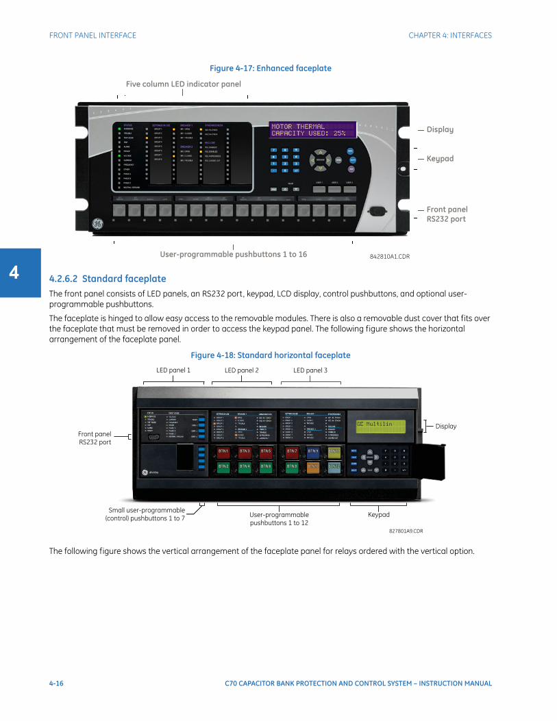
4-16 C70 CAPACITOR BANK PROTECTION AND CONTROL SYSTEM – INSTRUCTION MANUAL
FRONT PANEL INTERFACE CHAPTER 4: INTERFACES
4
Figure 4-17: Enhanced faceplate
4.2.6.2 Standard faceplateThe front panel consists of LED panels, an RS232 port, keypad, LCD display, control pushbuttons, and optional user-programmable pushbuttons.
The faceplate is hinged to allow easy access to the removable modules. There is also a removable dust cover that fits over the faceplate that must be removed in order to access the keypad panel. The following figure shows the horizontal arrangement of the faceplate panel.
Figure 4-18: Standard horizontal faceplate
The following figure shows the vertical arrangement of the faceplate panel for relays ordered with the vertical option.
Five column LED indicator panel
Display
User-programmable pushbuttons 1 to 16 842810A1.CDR
Keypad
Front panel
RS232 port

CHAPTER 4: INTERFACES FRONT PANEL INTERFACE
C70 CAPACITOR BANK PROTECTION AND CONTROL SYSTEM – INSTRUCTION MANUAL 4-17
4
Figure 4-19: Standard vertical faceplate
4.2.7 LED indicators
4.2.7.1 Enhanced faceplateThe enhanced front panel display provides five columns of LED indicators. The first column contains 14 status and event-cause LEDs. The next four columns contain the 48 user-programmable LEDs.
The RESET key is used to reset any latched LED indicator or target message, once the condition has been cleared (these latched conditions can also be reset via the SETTINGS INPUT/OUTPUTS RESETTING menu).
The USER keys are used by the breaker control feature.
Figure 4-20: Typical LED panel for enhanced faceplate
The status indicators in the first column are as follows:
842811A1.CDR
4-18 C70 CAPACITOR BANK PROTECTION AND CONTROL SYSTEM – INSTRUCTION MANUAL
FRONT PANEL INTERFACE CHAPTER 4: INTERFACES
4
• IN SERVICE — This LED indicates that control power is applied, all monitored inputs, outputs, and internal systems are OK, and that the device has been programmed
• TROUBLE — This LED indicates that the relay has detected an internal problem
• TEST MODE — This LED indicates that the relay is in test mode. For more information, see the Test Mode section in the Settings chapter.
• TRIP — This LED indicates that the FlexLogic operand serving as a trip switch has operated. This indicator always latches; as such, a reset command must be initiated to allow the latch to reset.
• ALARM — This LED indicates that the FlexLogic operand serving as an alarm switch has operated. This indicator is never latched.
• PICKUP — This LED indicates that an element is picked up. This indicator is never latched.
The event-cause indicators in the first column are as follows.
Event-cause LEDs are turned on or off by protection elements that have their respective target setting selected as either “Enabled” or “Latched.” If a protection element target setting is “Enabled,” then the corresponding event-cause LEDs remain on as long as the operate operand associated with the element remains asserted. If a protection element target setting is “Latched,” then the corresponding event-cause LEDs turn on when the operate operand associated with the element is asserted and remain on until the RESET button on the front panel is pressed after the operand is reset.
All elements that are able to discriminate faulted phases can independently turn off or on the phase A, B, or C LEDs. This includes phase instantaneous overcurrent, phase undervoltage, and so on. This means that the phase A, B, and C operate operands for individual protection elements are ORed to turn on or off the phase A, B, or C LEDs.
• VOLTAGE — This LED indicates voltage was involved
• CURRENT — This LED indicates current was involved
• FREQUENCY — This LED indicates frequency was involved
• OTHER — This LED indicates a composite function was involved
• PHASE A — This LED indicates phase A was involved
• PHASE B — This LED indicates phase B was involved
• PHASE C — This LED indicates phase C was involved
• NEUTRAL/GROUND — This LED indicates that neutral or ground was involved
The user-programmable LEDs consist of 48 amber LED indicators in four columns. The operation of these LEDs is user-defined. Support for applying a customized label beside every LED is provided. Default labels are shipped in the label package of every C70, together with custom templates. The default labels can be replaced by user-printed labels.
User customization of LED operation is of maximum benefit in installations where languages other than English are used to communicate with operators. See the User-Programmable LEDs section in chapter 5 for the settings used to program the operation of the LEDs on these panels.
4.2.7.2 Standard faceplateThe standard faceplate consists of three panels with LED indicators, keys, and a communications port. The RESET key is used to reset any latched LED indicator or target message, once the condition has been cleared (these latched conditions can also be reset via the SETTINGS INPUT/OUTPUTS RESETTING menu). The RS232 port is for connection to a computer.
The USER keys are used by the breaker control feature.

CHAPTER 4: INTERFACES FRONT PANEL INTERFACE
C70 CAPACITOR BANK PROTECTION AND CONTROL SYSTEM – INSTRUCTION MANUAL 4-19
4
Figure 4-21: LED panel 1
Status indicators• IN SERVICE — Indicates that control power is applied, all monitored inputs/outputs and internal systems are fine, the
relay has been programmed
• TROUBLE — Indicates that the relay has detected an internal problem
• TEST MODE — Indicates that the relay is in test mode. For more information, see the Test Mode section in the Settings chapter.
• TRIP — Indicates that the selected FlexLogic operand serving as a Trip switch has operated. This indicator always latches; the reset command must be initiated to allow the latch to be reset.
• ALARM — Indicates that the selected FlexLogic operand serving as an Alarm switch has operated. This indicator is never latched.
• PICKUP — Indicates that an element is picked up. This indicator is never latched.
Event-cause indicatorsEvent-cause LEDs are turned on or off by protection elements that have their respective target setting selected as either “Enabled” or “Latched.” If a protection element target setting is “Enabled,” then the corresponding event cause LEDs remain on as long as operate the operand associated with the element remains asserted. If a protection element target setting is “Latched,” then the corresponding event cause LEDs turn on when the operate operand associated with the element is asserted and remain on until the RESET button on the front panel is pressed after the operand is reset.
All elements that are able to discriminate faulted phases can independently turn off or on the phase A, B, or C LEDs. This includes phase instantaneous overcurrent, phase undervoltage, and so on. This means that the phase A, B, and C operate operands for individual protection elements are ORed to turn on or off the phase A, B, or C LEDs.
• VOLTAGE — Indicates voltage was involved
• CURRENT — Indicates current was involved
• FREQUENCY — Indicates frequency was involved
• OTHER — Indicates a composite function was involved
• PHASE A — Indicates phase A was involved
• PHASE B — Indicates phase B was involved
• PHASE C — Indicates phase C was involved
• NEUTRAL/GROUND — Indicates that neutral or ground was involved
User-programmable indicatorsThe second and third panels provide 48 amber LED indicators whose operation is controlled by the user. Support for applying a customized label beside every LED is provided.
User customization of LED operation is of maximum benefit in installations where languages other than English are used to communicate with operators. See the User-programmable LEDs section in chapter 5 for the settings used to program the operation of the LEDs on these panels.

4-20 C70 CAPACITOR BANK PROTECTION AND CONTROL SYSTEM – INSTRUCTION MANUAL
FRONT PANEL INTERFACE CHAPTER 4: INTERFACES
4
Figure 4-22: LED panels 2 and 3 (index template)
Default labels for LED panel 2The default labels are intended to represent the following:
• GROUP 1...6 — The illuminated GROUP is the active settings group
The relay is shipped with the default label for the LED panel 2. The LEDs, however, are not pre-programmed. To match the pre-printed label, the LED settings must be entered as shown in the User-programmable LEDs section of chapter 5. The LEDs are fully user-programmable. The default labels can be replaced by user-printed labels for both panels as explained in the next section.
Figure 4-23: LED panel 2 (default labels)
4.2.8 Custom LED labeling
4.2.8.1 Enhanced faceplateThe following procedure requires these pre-requisites:
• EnerVista UR Setup software is installed and operational
• The C70 settings have been saved to a settings file
• The UR front panel label cutout sheet (GE part number 1006-0047) has been downloaded from http://www.gedigitalenergy.com/products/support/ur/URLEDenhanced.doc and printed
• Small-bladed knife
To create custom LED labels for the enhanced front panel display:
1. Start the EnerVista UR Setup software.
2. Select the Front Panel Report item at the bottom of the navigation menu for the settings file. The front panel report window displays.
USER-PROGRAMMABLE LEDS USER-PROGRAMMABLE LEDS
842782A1.CDR

CHAPTER 4: INTERFACES FRONT PANEL INTERFACE
C70 CAPACITOR BANK PROTECTION AND CONTROL SYSTEM – INSTRUCTION MANUAL 4-21
4
Figure 4-24: Front panel report window
3. Enter the text to appear next to each LED and above each user-programmable pushbutton in the fields provided.
4. Feed the UR front panel label cutout sheet into a printer and press the Print button in the front panel report window.
5. When printing is complete, fold the sheet along the perforated lines and punch out the labels.
6. Remove the UR label insert tool from the package and bend the tabs as described in the following procedures. These tabs are used for removal of the default and custom LED labels.
The label package shipped with every C70 contains the three default labels, the custom label template sheet, and the label removal tool.
If the default labels are suitable for your application, insert them in the appropriate slots and program the LEDs to match them. If you require custom labels, use the following procedures to remove the original labels and insert the new ones.
To set up and use the label removal tool:
1. Bend the tabs at the left end of the tool upwards as shown.
NOTE
Use the tool EXACTLY as outlined as follows, with the printed side containing the GE part number facing the user.
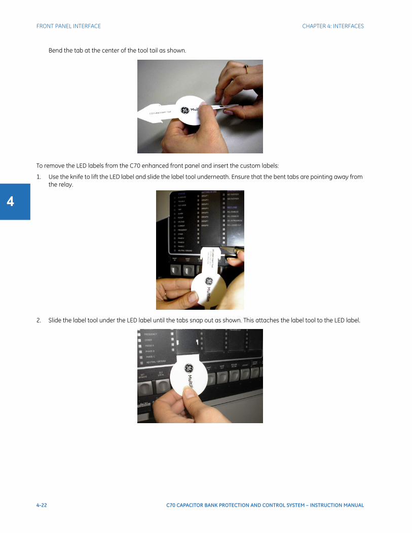
4-22 C70 CAPACITOR BANK PROTECTION AND CONTROL SYSTEM – INSTRUCTION MANUAL
FRONT PANEL INTERFACE CHAPTER 4: INTERFACES
4
Bend the tab at the center of the tool tail as shown.
To remove the LED labels from the C70 enhanced front panel and insert the custom labels:
1. Use the knife to lift the LED label and slide the label tool underneath. Ensure that the bent tabs are pointing away from the relay.
2. Slide the label tool under the LED label until the tabs snap out as shown. This attaches the label tool to the LED label.

CHAPTER 4: INTERFACES FRONT PANEL INTERFACE
C70 CAPACITOR BANK PROTECTION AND CONTROL SYSTEM – INSTRUCTION MANUAL 4-23
4
3. Remove the tool and attached LED label as shown.
4. Slide the new LED label inside the pocket until the text is properly aligned with the LEDs, as shown.
To remove the user-programmable pushbutton labels from the C70 enhanced front panel and insert the custom labels:
1. Use the knife to lift the pushbutton label and slide the tail of the label tool underneath, as shown. Ensure that the bent tab points away from the relay.
2. Slide the label tool under the user-programmable pushbutton label until the tabs snap out as shown. This attaches the

4-24 C70 CAPACITOR BANK PROTECTION AND CONTROL SYSTEM – INSTRUCTION MANUAL
FRONT PANEL INTERFACE CHAPTER 4: INTERFACES
4
label tool to the user-programmable pushbutton label.
3. Remove the tool and attached user-programmable pushbutton label.
4. Slide the new user-programmable pushbutton label inside the pocket until the text is properly aligned with the

CHAPTER 4: INTERFACES FRONT PANEL INTERFACE
C70 CAPACITOR BANK PROTECTION AND CONTROL SYSTEM – INSTRUCTION MANUAL 4-25
4
buttons.
4.2.9 Breaker controlThe C70 can interface with associated circuit breakers. In many cases the application monitors the state of the breaker, that can be presented on faceplate LEDs, along with a breaker trouble indication. Breaker operations can be manually initiated from the faceplate keypad or automatically initiated from a FlexLogic operand. A setting is provided to assign names to each breaker; this user-assigned name is for the display of related flash messages. These features are provided for two breakers; the user can use only those portions of the design relevant to a single breaker, which must be breaker 1.
It is assumed in the following discussion that the SETTINGS SYSTEM SETUP BREAKERS BREAKER 1(2) BREAKER FUNCTION setting is "Enabled" for each breaker.
4.2.9.1 Control mode selection and monitoringInstallations can require that a breaker be operated in the three-pole only mode (3-pole), or in the one and three-pole (1-pole) mode, selected by setting. If the mode is selected as three-pole, a single input tracks the breaker open or closed position. If the mode is selected as one-pole, all three breaker pole states must be input to the relay. These inputs must be in agreement to indicate the position of the breaker.
For the following discussion it is assumed that the SETTINGS SYSTEM SETUP BREAKERS BREAKER 1(2) BREAKER 1(2) PUSH BUTTON CONTROL setting is “Enabled” for each breaker.
4.2.9.2 Faceplate (user key) controlAfter the 30 minute interval during which command functions are permitted after a correct command password, the user cannot open or close a breaker via the keypad. The following discussions begin from the not-permitted state.
4.2.9.3 Control of two breakersFor the following setup example, the (Name) field represents the user-programmed variable name.
For this example, the relay is connected and programmed for both breaker 1 and breaker 2. The USER 1 key performs the selection of which breaker is to be operated by the USER 2 and USER 3 keys. The USER 2 key manually closes the breaker, and the USER 3 key manually opens the breaker.

4-26 C70 CAPACITOR BANK PROTECTION AND CONTROL SYSTEM – INSTRUCTION MANUAL
FRONT PANEL INTERFACE CHAPTER 4: INTERFACES
4
4.2.9.4 Control of one breakerFor this application, the relay is connected and programmed for breaker 1 only. Operation for this application is identical to that described in the previous section for two breakers.
4.2.10 Change passwordsThe information in this section refers to password security. For information on how to set the password for the first time or change CyberSentry passwords, see the previous chapter or the Settings > Product Setup > Security > CyberSentry section in the next chapter.
The C70 supports password entry from a local or remote connection.
Local access is defined as access to settings or commands via the faceplate. This includes both keypad entry and the RS232 port. Remote access is defined as access to settings or commands via any rear communications port. This includes both Ethernet and RS485 connections. Any change to the local or remote password enables this functionality.
When entering a settings or command password via EnerVista or any serial interface, the user must enter the corresponding connection password. If the connection is to the back of the C70, the remote password must be used. If the connection is to the RS232 port of the faceplate, the local password must be used.
There are two user security access levels, setting and command, for which you can set a password for each. Use of a password for each level controls whether users can enter commands or change settings. Another option is to specify setting and/or command access for individual user accounts.
• Setting — Allows the user to make any changes to any of the setting values:
– Changing any setting
– Test mode operation
• Command — Restricts the user from making any settings changes, but allows the user to perform the following operations:
– Changing the state of virtual inputs
– Clearing the event records
ENTER COMMANDPASSWORD
This message appears when the USER 1, USER 2, or USER 3 key is pressed and a COMMAND PASSWORD is required, that is, if COMMAND PASSWORD is enabled and no commands have been issued within the last 30 minutes.
Press USER 1To Select Breaker
This message appears if the correct password is entered or if none is required. This message displays for 30 seconds or until the USER 1 key is pressed again.
BKR1-(Name) SELECTEDUSER 2=CLS/USER 3=OP
This message displays after the USER 1 key is pressed for the second time. Three possible actions can be performed from this state within 30 seconds as per the following items (1), (2) and (3).
(1)
USER 2 OFF/ONTo Close BKR1-(Name)
If the USER 2 key is pressed, this message appears for 20 seconds. If the USER 2 key is pressed again within that time, a signal is created that can be programmed to operate an output relay to close breaker 1.
(2)
USER 3 OFF/ONTo Open BKR1-(Name)
If the USER 3 key is pressed, this message appears for 20 seconds. If the USER 3 key is pressed again within that time, a signal is created that can be programmed to operate an output relay to open breaker 1.
(3)
BKR2-(Name) SELECTEDUSER 2=CLS/USER 3=OP
If the USER 1 key is pressed at this step, this message appears showing that a different breaker is selected. Three possible actions can be performed from this state as per (1), (2) and (3). Repeatedly pressing the USER 1 key alternates between available breakers. Pressing keys other than USER 1, 2, or 3 at any time cancels the breaker control function.
CHAPTER 4: INTERFACES FRONT PANEL INTERFACE
C70 CAPACITOR BANK PROTECTION AND CONTROL SYSTEM – INSTRUCTION MANUAL 4-27
4
– Clearing the oscillography records
– Changing the date and time
– Clearing the data logger
– Clearing the user-programmable pushbutton states
To enter the initial setting or command password:
1. Press the MENU key until the SETTINGS header flashes momentarily and the PRODUCT SETUP message appears on the display.
2. Press the MESSAGE right arrow until the ACCESS LEVEL message appears on the display.
3. Press the MESSAGE down arrow until the CHANGE LOCAL PASSWORDS message appears on the display.
4. Press the MESSAGE right arrow until the CHANGE SETTING PASSWORD or CHANGE COMMAND PASSWORD message appears on the display.
5. After the CHANGE...PASSWORD message appears on the display, press the VALUE up or down arrow to change the selection to “Yes.”
6. Press the ENTER key and the display prompts you to ENTER NEW PASSWORD.
7. Type in a numerical password (up to 10 characters) and press the ENTER key.
8. When VERIFY NEW PASSWORD displays, re-type the password and press ENTER.
9. When the NEW PASSWORD HAS BEEN STORED message appears, your new Setting (or Command) password is active.
4.2.11 Invalid password entryBy default, when an incorrect Command or Setting password has been entered via the faceplate interface three times within five minutes, the LOCAL ACCESS DENIED FlexLogic operand is set to “On” and the C70 does not allow settings or command level access via the faceplate interface for five minutes.
By default, when an incorrect Command or Setting password has been entered via any external communications interface three times within five minutes, the REMOTE ACCESS DENIED FlexLogic operand is set to “On” and the C70 does not allow settings or command access via the any external communications interface for five minutes. The REMOTE ACCESS DENIED FlexLogic operand is set to “Off” after five minutes for a Command password or 30 minutes for a Settings password.
These default settings can be changed in EnerVista under Settings > Product Setup > Security.
SECURITY ACCESS LEVEL:
Restricted
CHANGE LOCAL PASSWORDS CHANGE COMMAND
PASSWORD: No
CHANGE SETTINGPASSWORD: No
ENCRYPTED COMMANDPASSWORD: ---------
ENCRYPTED SETTINGPASSWORD: ---------
CHANGE SETTINGPASSWORD: No
CHANGE SETTINGPASSWORD: Yes
ENTER NEWPASSWORD: ##########
VERIFY NEWPASSWORD: ##########
NEW PASSWORDHAS BEEN STORED

4-28 C70 CAPACITOR BANK PROTECTION AND CONTROL SYSTEM – INSTRUCTION MANUAL
LOGIC DIAGRAMS CHAPTER 4: INTERFACES
4
4.3 Logic diagramsLogic diagrams in this instruction manual provide an overview of function and settings. A logic diagram is based on
• Inputs-on the left side, which are setting and operands
• Logical gates, which is Boolean algebra to combine logical lines using AND, OR, NOT, and other gates to get a new logical state
• Logical operators, which are timers, one-shot operations, latches, and so on
• Outputs-on the right side, which are products of the manipulations with inputs, logical gates, and logical operators to produce new operands and define the output state of the element
True and false values are denoted by 1 and 0 respectively. A function usually is high/on/enabled when 1.
Reading from right to left in the following diagram, the TRIP BUS 1 OP and TRIP BUS 1 PKP FlexLogic operands on the right side are triggered when either the settings or reset latch in the middle of the diagram is triggered. When this applies, the TRIP BUS 1 OP operand is triggered after the delay set by the TRIP BUS 1 PICKUP DELAY or TRIP BUS 1 RESET DELAY setting, while the TRIP BUS 1 PKP operand initiates immediately. The settings or reset latch in the middle of the diagram is triggered as follows.
• For the reset, one of three conditions are required to meet the OR requirement shown at the bottom left. That is, the TRIP BUS 1 LATCHING setting must be 0=Disabled (which is negated by the NOT function to become 1=Enabled), output from the TRIP BUS 1 RESET FlexLogic operand must be 1, or output from the RESET OP FlexLogic operand must be 1.
• For the settings, one of 16 input conditions at the top left must be met for the OR, the TRIP BUS 1 FUNCTION must be Enabled, and the TRIP BUS 1 BLOCK output must output as 0, which is then negated/reversed by NOT to become 1.
Table 4-1: Logic diagram symbols
Figure 4-25: Logic diagram
Symbol Description
= Off Output from FlexLogic operand, so user-defined
= Enabled 1 = Enabled and 0 = Disabled
OR Any function input on the left side satisfies the condition
AND All functions input on the left side are required to satisfy the condition
Not. Negates/reverses the output, for example 0 becomes 1.
Connection
S, R Set, Reset
TPKP Timer pickup. Triggered by the settings latch in the diagram.
TRST Timer reset. Triggered by the reset latch in the diagram.
**
*
SETTINGS
= Off
TRIP BUS 1 INPUT 2
= Off
TRIP BUS 1 INPUT 1
= Off
TRIP BUS 1 INPUT 16
OR
SETTINGS
= Enabled
TRIP BUS 1
FUNCTION
= Off
TRIP BUS 1 BLOCK AND
AND
Latch
S
R
Non-volatile,
set-dominant
SETTINGS
= Enabled
TRIP BUS 1
LATCHING
= Off
TRIP BUS 1 RESET
FLEXLOGIC OPERAND
TRIP BUS 1 PKP
OR
SETTINGS
TRIP BUS 1 PICKUP
DELAY
TRIP BUS 1 RESET
DELAY
TPKP
TRST
FLEXLOGIC OPERAND
RESET OP
FLEXLOGIC OPERAND
TRIP BUS 1 OP
842023A1.CDR

CHAPTER 4: INTERFACES LOGIC DIAGRAMS
C70 CAPACITOR BANK PROTECTION AND CONTROL SYSTEM – INSTRUCTION MANUAL 4-29
4

4-30 C70 CAPACITOR BANK PROTECTION AND CONTROL SYSTEM – INSTRUCTION MANUAL
LOGIC DIAGRAMS CHAPTER 4: INTERFACES
4
C70 CAPACITOR BANK PROTECTION AND CONTROL SYSTEM – INSTRUCTION MANUAL 5-1
C70 Capacitor Bank Protection and Control System
Chapter 5: Settings
Settings
This chapter outlines front panel and/or software settings. The relay is not taken out of service when saving settings; the relay is taken out of service when a settings file is written to it .
5.1 Settings menu
SETTINGS PRODUCT SETUP SECURITY
See page 5-7
DISPLAY PROPERTIES
See page 5-25
CLEAR RELAY RECORDS
See page 5-27
COMMUNICATIONS
See page 5-27
MODBUS USER MAP
See page 5-82
REAL TIME CLOCK
See page 5-82
USER-PROGRAMMABLE FAULT REPORT
See page 5-86
OSCILLOGRAPHY
See page 5-87
DATA LOGGER
See page 5-89
USER-PROGRAMMABLE LEDS
See page 5-90
USER-PROGRAMMABLE SELF TESTS
See page 5-94
CONTROL PUSHBUTTONS
See page 5-94

5-2 C70 CAPACITOR BANK PROTECTION AND CONTROL SYSTEM – INSTRUCTION MANUAL
SETTINGS MENU CHAPTER 5: SETTINGS
5
USER-PROGRAMMABLE PUSHBUTTONS
See page 5-96
FLEX STATE PARAMETERS
See page 5-101
USER-DEFINABLE DISPLAYS
See page 5-102
DIRECT I/O
See page 5-104
INSTALLATION
See page 5-111
REMOTE RESOURCES
Access in EnerVistaSee page 5-111
SETTINGS SYSTEM SETUP AC INPUTS
See page 5-112
POWER SYSTEM
See page 5-114
SIGNAL SOURCES
See page 5-114
BREAKERS
See page 5-117
SWITCHES
See page 5-122
FLEXCURVES
See page 5-125
SETTINGS FLEXLOGIC FLEXLOGIC
EQUATION EDITORSee page 5-151
FLEXLOGIC TIMERS
See page 5-151
FLEXELEMENTS
See page 5-151
NON-VOLATILE LATCHES
See page 5-155
SETTINGS GROUPED ELEMENTS SETTING GROUP 1
See page 5-156
SETTING GROUP 2
SETTING GROUP 3
SETTING GROUP 4
SETTING GROUP 5
SETTING GROUP 6
SETTINGS CONTROL ELEMENTS TRIP BUS
See page 5-217
SETTING GROUPS
See page 5-219
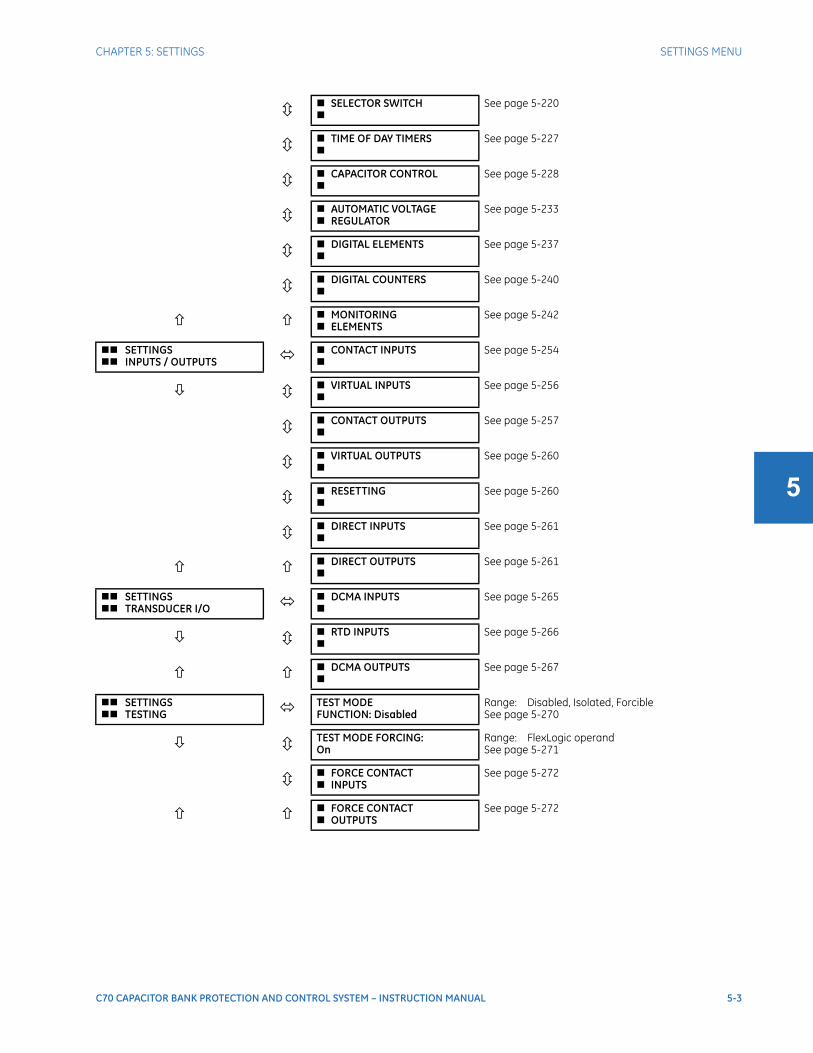
CHAPTER 5: SETTINGS SETTINGS MENU
C70 CAPACITOR BANK PROTECTION AND CONTROL SYSTEM – INSTRUCTION MANUAL 5-3
5
SELECTOR SWITCH
See page 5-220
TIME OF DAY TIMERS
See page 5-227
CAPACITOR CONTROL
See page 5-228
AUTOMATIC VOLTAGE REGULATOR
See page 5-233
DIGITAL ELEMENTS
See page 5-237
DIGITAL COUNTERS
See page 5-240
MONITORING ELEMENTS
See page 5-242
SETTINGS INPUTS / OUTPUTS CONTACT INPUTS
See page 5-254
VIRTUAL INPUTS
See page 5-256
CONTACT OUTPUTS
See page 5-257
VIRTUAL OUTPUTS
See page 5-260
RESETTING
See page 5-260
DIRECT INPUTS
See page 5-261
DIRECT OUTPUTS
See page 5-261
SETTINGS TRANSDUCER I/O DCMA INPUTS
See page 5-265
RTD INPUTS
See page 5-266
DCMA OUTPUTS
See page 5-267
SETTINGS TESTING TEST MODE
FUNCTION: DisabledRange: Disabled, Isolated, ForcibleSee page 5-270
TEST MODE FORCING:On
Range: FlexLogic operandSee page 5-271
FORCE CONTACT INPUTS
See page 5-272
FORCE CONTACT OUTPUTS
See page 5-272

5-4 C70 CAPACITOR BANK PROTECTION AND CONTROL SYSTEM – INSTRUCTION MANUAL
OVERVIEW CHAPTER 5: SETTINGS
5
5.2 Overview
5.2.1 Introduction to elementsFor URs, the term element is used to describe a feature that is based around a comparator. The comparator is provided with an input (or set of inputs) that is tested against a programmed setting (or group of settings) to determine if the input is within the defined range that sets the output to logic 1, also referred to as setting the flag. A single comparator can make multiple tests and provide multiple outputs. For example, the time overcurrent comparator sets a pickup flag when the current input is above the setting and sets an operate flag when the input current has been at a level above the pickup setting for the time specified by the time-current curve settings. All comparators use analog actual values as the input.
Elements are arranged into two classes, grouped and control. Each element classed as a grouped element is provided with six alternate sets of settings, in setting groups numbered 1 through 6. The performance of a grouped element is defined by the setting group that is active at a given time. The performance of a control element is independent of the selected active setting group.
The main characteristics of an element are shown on a logic diagram. This includes the inputs, settings, fixed logic, and the output operands generated. The previous chapter explains how to read a logic diagram, and the abbreviations used in a diagram are defined in the Abbreviations chapter.
Some settings are specified in per-unit (pu) calculated quantities:
pu quantity = (actual quantity) / (base quantity)
Where the current source is from a single current transformer (CT), the base quantity is the nominal secondary or primary current of the CT. Use the secondary current base to convert per-unit settings to/from a secondary current value, and use the primary current base to convert to/from a primary current value.
Where the current source is the sum of two or more CTs with different nominal primary current, the primary base quantity is the largest nominal primary current. For example, if CT1 = 300 / 5 A and CT2 = 100 / 1 A, then in order to sum these, CT2 is scaled to the CT1 ratio. In this case, the base quantity is 300 A primary, 5 A secondary for CT1, and 300/(100/1) = 3 A secondary for CT2.
For voltage elements, the primary base quantity is the nominal phase-to-phase primary voltage of the protected system provided that the VT ratio setting is set to the nominal ratio of the VTs and the secondary voltage setting is set to the phase-to-phase voltage seen by the relay when the voltage of the protected system in nominal. The UR uses the convention that nominal voltages in a three-phase system are phase-to-phase voltages.
For example, on a system with a 13.8 kV nominal primary voltage, the base quantity is 13800 V. With 14400:120 V delta-connected VTs, the secondary base quantity and secondary voltage setting is:
Eq. 5-1
For wye-connected VTs, the primary and secondary base quantities are as before, but the secondary voltage setting (herea phase-to-ground value) is:
Eq. 5-2
Many settings are common to most elements, outlined as follows:
• FUNCTION setting — This setting programs the element to operate when selected as “Enabled.” The factory default is “Disabled.” Once “Enabled,” any element associated with the function becomes active and all options become available.
• NAME setting — This setting is used to uniquely identify the element.
NOTE
An exception to this rule is digital elements, which use logic states as inputs.
1380014400-------------- 120× 115 V=
1380014400-------------- 120
3--------× 66.4 V=

CHAPTER 5: SETTINGS OVERVIEW
C70 CAPACITOR BANK PROTECTION AND CONTROL SYSTEM – INSTRUCTION MANUAL 5-5
5
• SOURCE setting — This setting is used to select the AC source to be monitored. See the Introduction to AC Sources section later.
• PICKUP setting — For simple elements, this setting is used to program the level of the measured parameter above or below which the pickup state is established. In more complex elements, a set of settings can be provided to define the range of the measured parameters that cause the element to pick up.
• PICKUP DELAY setting — This setting sets a time-delay-on-pickup, or on-delay, for the duration between the pickup and operate output states.
• RESET DELAY setting — This setting is used to set a time-delay-on-dropout, or off-delay, for the duration between the operate output state and the return to logic 0 after the input transits outside the defined pickup range.
• BLOCK setting — The default output operand state of all comparators is a logic 0 or “flag not set.” The comparator remains in this default state until a logic 1 is asserted at the RUN input, allowing the test to be performed. If the RUN input changes to logic 0 at any time, the comparator returns to the default state. The RUN input is used to supervise the comparator. The BLOCK input is used as one of the inputs to RUN control.
• TARGET setting — This setting is used to define the operation of an element target message. When set to "Disabled," no target message or illumination of a faceplate LED indicator is issued upon operation of the element. When set to “Self-Reset,” the target message and LED indication follow the operate state of the element and self-resets once the operate element condition clears. When set to “Latched,” the target message and LED indication remains visible after the element output returns to logic 0 until a RESET command is received by the relay.
• EVENTS setting — This setting is used to control whether the pickup, dropout, or operate states are recorded by the event recorder. When set to “Disabled,” element pickup, dropout, or operate are not recorded as events. When set to “Enabled,” events are created for
<Element> PKP (pickup)<Element> DPO (dropout)<Element> OP (operate)
The DPO event is created when the measure and decide comparator output transits from the pickup state (logic 1) to the dropout state (logic 0). This can happen when the element is in the operate state if the reset delay time is not zero.
Not every operand of a given element in a UR relay generates events, only the major output operands. Elements, asserting output per phase, log operating phase output only, without asserting the common three-phase operand event.
5.2.2 Introduction to AC sources
5.2.2.1 BackgroundA mechanism called a source configures the routing of CT and VT input channels to measurement sub-systems. Sources, in the context of UR series relays, refer to the logical grouping of current and voltage signals such that one source contains all the signals required to measure the load or fault in a particular power apparatus. A given source can contain all or some of the following signals: three-phase currents, single-phase ground current, three-phase voltages, and an auxiliary voltage from a single VT for checking for synchronism.
The basic idea of an AC source is to select a point on the power system where the voltages and currents are of interest. To illustrate the concept of sources, as applied to current inputs only, consider the breaker-and-a-half scheme that follows. In this application, the current flows as shown by the arrows. Some current flows through the upper bus bar to some other location or power equipment, and some current flows into transformer winding 1. The current into winding 1 is the phasor sum (or difference) of the currents in CT1 and CT2 (whether the sum or difference is used depends on the relative polarity of the CT connections). The same considerations apply to transformer winding 2. The protection elements require access to the net current for transformer protection, but some elements can need access to the individual currents from CT1 and CT2.
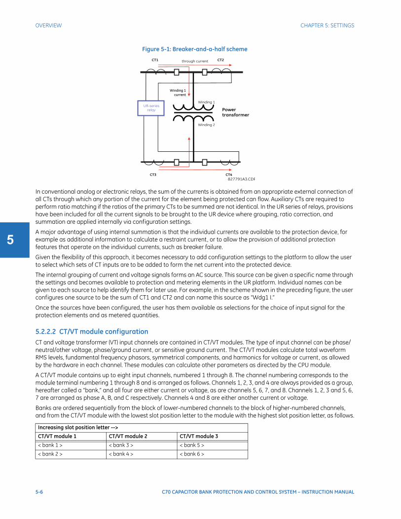
5-6 C70 CAPACITOR BANK PROTECTION AND CONTROL SYSTEM – INSTRUCTION MANUAL
OVERVIEW CHAPTER 5: SETTINGS
5
Figure 5-1: Breaker-and-a-half scheme
In conventional analog or electronic relays, the sum of the currents is obtained from an appropriate external connection of all CTs through which any portion of the current for the element being protected can flow. Auxiliary CTs are required to perform ratio matching if the ratios of the primary CTs to be summed are not identical. In the UR series of relays, provisions have been included for all the current signals to be brought to the UR device where grouping, ratio correction, and summation are applied internally via configuration settings.
A major advantage of using internal summation is that the individual currents are available to the protection device, for example as additional information to calculate a restraint current, or to allow the provision of additional protection features that operate on the individual currents, such as breaker failure.
Given the flexibility of this approach, it becomes necessary to add configuration settings to the platform to allow the user to select which sets of CT inputs are to be added to form the net current into the protected device.
The internal grouping of current and voltage signals forms an AC source. This source can be given a specific name through the settings and becomes available to protection and metering elements in the UR platform. Individual names can be given to each source to help identify them for later use. For example, in the scheme shown in the preceding figure, the user configures one source to be the sum of CT1 and CT2 and can name this source as “Wdg1 I.”
Once the sources have been configured, the user has them available as selections for the choice of input signal for the protection elements and as metered quantities.
5.2.2.2 CT/VT module configurationCT and voltage transformer (VT) input channels are contained in CT/VT modules. The type of input channel can be phase/neutral/other voltage, phase/ground current, or sensitive ground current. The CT/VT modules calculate total waveform RMS levels, fundamental frequency phasors, symmetrical components, and harmonics for voltage or current, as allowed by the hardware in each channel. These modules can calculate other parameters as directed by the CPU module.
A CT/VT module contains up to eight input channels, numbered 1 through 8. The channel numbering corresponds to the module terminal numbering 1 through 8 and is arranged as follows. Channels 1, 2, 3, and 4 are always provided as a group, hereafter called a “bank,” and all four are either current or voltage, as are channels 5, 6, 7, and 8. Channels 1, 2, 3 and 5, 6, 7 are arranged as phase A, B, and C respectively. Channels 4 and 8 are either another current or voltage.
Banks are ordered sequentially from the block of lower-numbered channels to the block of higher-numbered channels, and from the CT/VT module with the lowest slot position letter to the module with the highest slot position letter, as follows.
Increasing slot position letter -->
CT/VT module 1 CT/VT module 2 CT/VT module 3
< bank 1 > < bank 3 > < bank 5 >
< bank 2 > < bank 4 > < bank 6 >

CHAPTER 5: SETTINGS PRODUCT SETUP
C70 CAPACITOR BANK PROTECTION AND CONTROL SYSTEM – INSTRUCTION MANUAL 5-7
5
The UR platform allows for a maximum of six sets of three-phase voltages and six sets of three-phase currents. The result of these restrictions leads to the maximum number of CT/VT modules in a chassis to three. The maximum number of sources is six. A summary of CT/VT module configurations is as follows.
5.2.2.3 CT/VT input channel configurationUpon relay startup, configuration settings for every bank of current or voltage input channels in the relay are generated automatically from the order code. Within each bank, a channel identification label is assigned automatically to each bank of channels in a given product. The bank naming convention is based on the physical location of the channels, required by the user to know how to connect the relay to external circuits. Bank identification consists of the letter designation of the slot in which the CT/VT module is mounted as the first character, followed by numbers indicating the channel, either 1 or 5. See the HardFiber instruction manual for designations of HardFiber voltage and current banks.
For three-phase channel sets, the number of the lowest numbered channel identifies the set. For example, F1 represents the three-phase channel set of F1/F2/F3, where F is the slot letter and 1 is the first channel of the three channels.
Upon startup, the CPU configures the settings required to characterize the current and voltage inputs, and it displays them in the appropriate section in the sequence of the banks (as described earlier) as follows for a maximum configuration: F1, F5, M1, M5, U1, and U5.
5.3 Product setup
5.3.1 Security
5.3.1.1 Security overviewThe following security features are available:
• Password security — Basic security present by default
• EnerVista security — Role-based access to various EnerVista software screens and configuration elements. The feature is present by default in the EnerVista software.
• CyberSentry security — Advanced security available as a software option. When purchased, the options are automatically enabled, and the default Password security and EnerVista security are disabled.
Lost passwordIf all passwords are lost, recovery is possible by resetting the unit to default values. Note that the relay is reset to default values, not just the passwords.
To reset the unit after a lost password:
1. Email GE customer service at [email protected] with the serial number and using a recognizable corporate email account. Customer service provides a code to reset the relay to the factory defaults.
2. Enter the reset code on the front panel, under COMMANDS RELAY MAINTENANCE SERVICE COMMAND.
3. Change the default password of ChangeMe1# as outlined in the Set Up CyberSentry and Change Default Password section at the end of the Installation chapter.
Password requirementsA user account requires an alpha-numeric password that meets the following requirements:
• Password is case-sensitive
Item Maximum number
CT/VT Module 3
CT Bank (3 phase channels, 1 ground channel) 6
VT Bank (3 phase channels, 1 auxiliary channel) 6

5-8 C70 CAPACITOR BANK PROTECTION AND CONTROL SYSTEM – INSTRUCTION MANUAL
PRODUCT SETUP CHAPTER 5: SETTINGS
5
• Password cannot contain the user account name or parts of the user account that exceed two consecutive characters
• Password must be 6 to 20 characters in length
• Password must contain characters from three of the following four categories:
– English uppercase characters (A through Z)
– English lowercase characters (a through z)
– Base 10 digits (0 through 9)
– Non-alphabetic characters (for example, ~, !, @, #, $,%, &)
5.3.1.2 Password securitySETTINGS PRODUCT SETUP SECURITY
The C70 supports password entry from a local or remote connection.
Local access is defined as access to settings or commands via the faceplate. This includes both keypad entry and the RS232 port. Remote access is defined as access to settings or commands via any rear communications port. This includes both Ethernet and RS485 connections. Any change to the local or remote password enables this functionality.
ACCESS LEVEL — The "Restricted" option means that settings and commands can be accessed, but there is no access to factory configuration. Access automatically reverts to the Restricted level according to the access level timeout setting values. The access level is set to Restricted when control power is cycled.
The "Factory Service" level is not available and intended for factory use only.
There are two user security access levels, setting and command, for which you can set a password for each. Use of a password for each level controls whether users can enter commands or change settings. Another option is to specify setting and/or command access for individual user accounts.
• Setting — Allows the user to make any changes to any of the setting values:
– Changing any setting
– Test mode operation
• Command — Restricts the user from making any settings changes, but allows the user to perform the following operations:
– Changing the state of virtual inputs
– Clearing the event records
– Clearing the oscillography records
– Changing the date and time
– Clearing the data logger
– Clearing the user-programmable pushbutton states
SECURITY ACCESS LEVEL:
RestrictedRange: Restricted, Command, Setting,Factory Service (for factory use only)
CHANGE LOCAL PASSWORDS
See page 5-9
CHANGE REMOTE PASSWORDS
See page 5-10
AC CESS SUPERVISION
See page 5-10
DUAL PERMISSION SECURITY ACCESS
See page 5-11
PASSWORD ACCESS:EVENTS: Disabled
Range: Disabled, Enabled
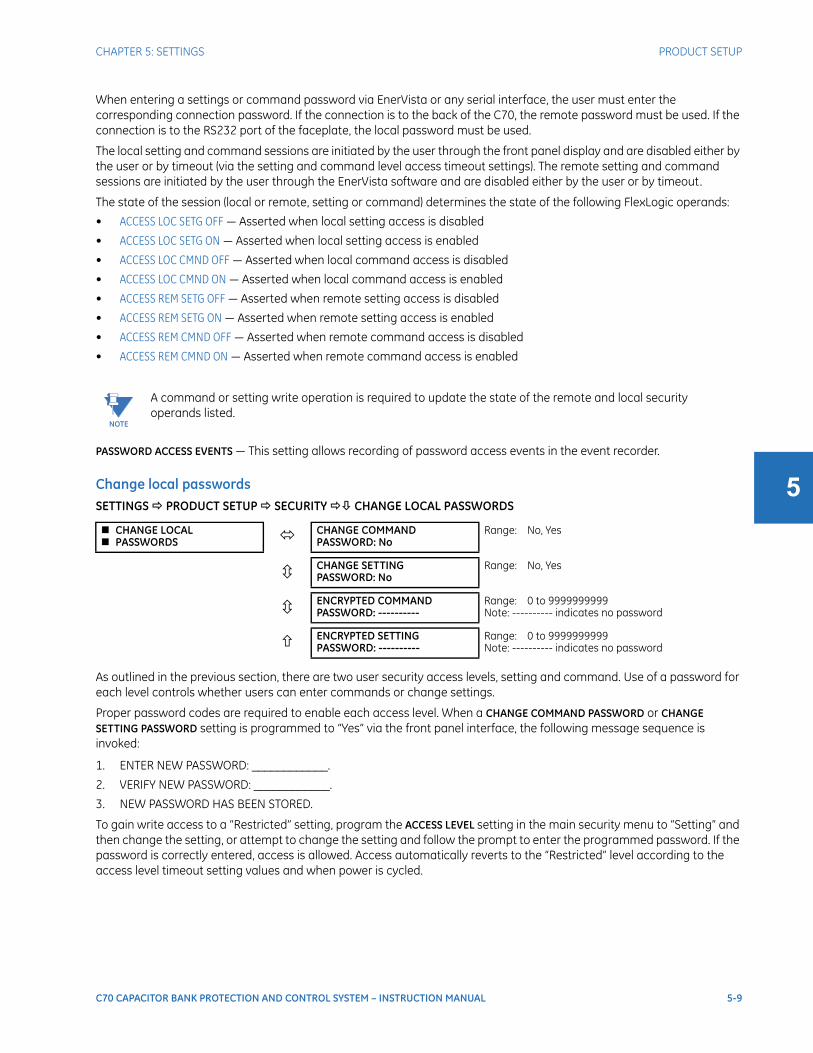
CHAPTER 5: SETTINGS PRODUCT SETUP
C70 CAPACITOR BANK PROTECTION AND CONTROL SYSTEM – INSTRUCTION MANUAL 5-9
5
When entering a settings or command password via EnerVista or any serial interface, the user must enter the corresponding connection password. If the connection is to the back of the C70, the remote password must be used. If the connection is to the RS232 port of the faceplate, the local password must be used.
The local setting and command sessions are initiated by the user through the front panel display and are disabled either by the user or by timeout (via the setting and command level access timeout settings). The remote setting and command sessions are initiated by the user through the EnerVista software and are disabled either by the user or by timeout.
The state of the session (local or remote, setting or command) determines the state of the following FlexLogic operands:
• ACCESS LOC SETG OFF — Asserted when local setting access is disabled
• ACCESS LOC SETG ON — Asserted when local setting access is enabled
• ACCESS LOC CMND OFF — Asserted when local command access is disabled
• ACCESS LOC CMND ON — Asserted when local command access is enabled
• ACCESS REM SETG OFF — Asserted when remote setting access is disabled
• ACCESS REM SETG ON — Asserted when remote setting access is enabled
• ACCESS REM CMND OFF — Asserted when remote command access is disabled
• ACCESS REM CMND ON — Asserted when remote command access is enabled
PASSWORD ACCESS EVENTS — This setting allows recording of password access events in the event recorder.
Change local passwordsSETTINGS PRODUCT SETUP SECURITY CHANGE LOCAL PASSWORDS
As outlined in the previous section, there are two user security access levels, setting and command. Use of a password for each level controls whether users can enter commands or change settings.
Proper password codes are required to enable each access level. When a CHANGE COMMAND PASSWORD or CHANGE SETTING PASSWORD setting is programmed to “Yes” via the front panel interface, the following message sequence is invoked:
1. ENTER NEW PASSWORD: ____________.
2. VERIFY NEW PASSWORD: ____________.
3. NEW PASSWORD HAS BEEN STORED.
To gain write access to a “Restricted” setting, program the ACCESS LEVEL setting in the main security menu to “Setting” and then change the setting, or attempt to change the setting and follow the prompt to enter the programmed password. If the password is correctly entered, access is allowed. Access automatically reverts to the “Restricted” level according to the access level timeout setting values and when power is cycled.
NOTE
A command or setting write operation is required to update the state of the remote and local security operands listed.
CHANGE LOCAL PASSWORDS CHANGE COMMAND
PASSWORD: NoRange: No, Yes
CHANGE SETTINGPASSWORD: No
Range: No, Yes
ENCRYPTED COMMANDPASSWORD: ----------
Range: 0 to 9999999999Note: ---------- indicates no password
ENCRYPTED SETTINGPASSWORD: ----------
Range: 0 to 9999999999Note: ---------- indicates no password

5-10 C70 CAPACITOR BANK PROTECTION AND CONTROL SYSTEM – INSTRUCTION MANUAL
PRODUCT SETUP CHAPTER 5: SETTINGS
5
Change remote passwordsProper passwords are required to enable each command or setting level access, which are explained in the previous section.
To set the command or setting password:
1. In the EnerVista software or from the front panel, navigate to Settings > Product Setup > Security menu item to open the remote password settings window.
2. Click the command or setting password Change button.
3. Enter the new password in the New Password field. Requirements are outlined in the Password Requirements section earlier in this chapter. When an original password has already been used, enter it in the Enter Password field and click the Send Password to Device button.
4. Re-enter the password in the Confirm Password field.
5. Click the OK button. The password is checked to ensure that it meets requirements.
Access supervisionSETTINGS PRODUCT SETUP SECURITY ACCESS SUPERVISION
The following access supervision settings are available.
INVALID ATTEMPTS BEFORE LOCKOUT — This setting specifies the number of times that an incorrect password can be entered within a three-minute time span before lockout occurs. When lockout occurs, the LOCAL ACCESS DENIED or REMOTE ACCESS DENIED FlexLogic operands are set to “On.” These operands are returned to the “Off” state upon expiration of the lockout.
PASSWORD LOCKOUT DURATION — This setting specifies the time that the C70 locks out password access after the number of invalid password entries specified by the INVALID ATTEMPTS BEFORE LOCKOUT setting has occurred.
NOTE
If the setting and command passwords are identical, then this one password allows access to both commands and settings.If a remote connection is established, local passcodes are not visible.
NOTE
If you establish a local (serial) connection to the relay, you cannot view remote passcodes.
ACCESS SUPERVISION ACCESS LEVEL
TIMEOUTSSee below
INVALID ATTEMPTSBEFORE LOCKOUT: 3
Range: 2 to 5 in steps of 1
PASSWORD LOCKOUTDURATION: 5 min
Range: 5 to 60 minutes in steps of 1

CHAPTER 5: SETTINGS PRODUCT SETUP
C70 CAPACITOR BANK PROTECTION AND CONTROL SYSTEM – INSTRUCTION MANUAL 5-11
5
The C70 provides a means to raise an alarm upon failed password entry. If password verification fails while accessing a password-protected level of the relay (either settings or commands), the UNAUTHORIZED ACCESS FlexLogic operand is asserted. The operand can be programmed to raise an alarm via contact outputs or communications. This feature can be used to protect against both unauthorized and accidental access attempts.
The UNAUTHORIZED ACCESS operand is reset with the COMMANDS CLEAR RECORDS RESET UNAUTHORIZED ALARMS command. Therefore, to apply this feature with security, password-protect the Command level. The operand does not generate events or targets.
If events or targets are required, the UNAUTHORIZED ACCESS operand can be assigned to a digital element programmed with event logs or targets enabled.
The following table outlines access level timeout settings.
SETTINGS PRODUCT SETUP SECURITY ACCESS SUPERVISION ACCESS LEVEL TIMEOUTS
These settings allow the user to specify the length of inactivity required before returning to the Restricted access level. Note that the access level is set to Restricted when control power is cycled.
COMMAND LEVEL ACCESS TIMEOUT — This setting specifies the length of inactivity (no local or remote access) required to return to Restricted access from the Command password level.
SETTING LEVEL ACCESS TIMEOUT — This setting specifies the length of inactivity (no local or remote access) required to return to Restricted access from the Command password level.
Dual-permission security accessSETTINGS PRODUCT SETUP SECURITY DUAL PERMISSION SECURITY ACCESS
This feature provides a mechanism to prevent unauthorized or unintended upload of settings to a relay through the local or remote interface.
The following settings are available through the local (front panel) interface only.
• LOCAL SETTING AUTH — This setting is used for local (front panel or RS232 interface) setting access supervision. Valid values for the FlexLogic operands are either “On” (default) or any physical “Contact Input ~~ On” value.
If this setting is “On,“ then local setting access functions as normal; that is, a local setting password is required. If this setting is any contact input on FlexLogic operand, then the operand must be asserted (on) prior to providing the local setting password to gain setting access.
If setting access is not authorized for local operation (front panel or RS232 interface) and the user attempts to obtain setting access, then the UNAUTHORIZED ACCESS message displays on the front panel.
If this setting is "Off," firmware upgrades are blocked. If this setting is "On," firmware upgrades are allowed.
• REMOTE SETTING AUTH — This setting is used for remote (Ethernet or RS485 interface) setting access supervision.
If this setting is “On” (the default setting), then remote setting access functions as normal; that is, a remote password is required. If this setting is “Off,” then remote setting access is blocked even if the correct remote setting password is provided. If this setting is any other FlexLogic operand, then the operand must be asserted (set as on) prior to providing the remote setting password to gain setting access.
If this setting is "Off," firmware upgrades are blocked. If this setting is "On," firmware upgrades are allowed.
ACCESS LEVEL TIMEOUTS COMMAND LEVEL ACCESS
TIMEOUT: 5 minRange: 5 to 480 minutes in steps of 1
SETTING LEVEL ACCESSTIMEOUT: 30 min
Range: 5 to 480 minutes in steps of 1
DUAL PERMISSION SECURITY ACCESS LOCAL SETTING AUTH:
OnRange: selected FlexLogic operands (see below)
REMOTE SETTING AUTH:On
Range: FlexLogic operand
ACCESS AUTHTIMEOUT: 30 min.
Range: 5 to 480 minutes in steps of 1

5-12 C70 CAPACITOR BANK PROTECTION AND CONTROL SYSTEM – INSTRUCTION MANUAL
PRODUCT SETUP CHAPTER 5: SETTINGS
5
• ACCESS AUTH TIMEOUT — This setting represents the timeout delay for local setting access. This setting is applicable when the LOCAL SETTING AUTH setting is programmed to any operand except “On.” The state of the FlexLogic operand is monitored continuously for an off-to-on transition. When this occurs, local access is permitted and the timer programmed with the ACCESS AUTH TIMEOUT setting value is started. When this timer expires, local setting access is immediately denied. If access is permitted and an off-to-on transition of the FlexLogic operand is detected, the timeout is restarted. The status of this timer updates every five seconds.
The following settings are available through the remote (EnerVista UR Setup) interface only. Select the Settings > Product Setup > Security menu item to display the security settings window.
The Remote Settings Authorized setting is used for remote (Ethernet or RS485 interface) setting access supervision. If this setting is “On” (the default setting), then remote setting access functions as normal; that is, a remote password is required). If this setting is “Off,” then remote setting access is blocked even if the correct remote setting password is provided. If this setting is any other FlexLogic operand, then the operand must be asserted (on) prior to providing the remote setting password to gain setting access.
The Access Authorized Timeout setting represents the timeout delay remote setting access. It applies when the Remote Settings Authorized setting is programmed to any operand except “On” or “Off.” The state of the FlexLogic operand is continuously monitored for an off-to-on transition. When this occurs, remote setting access is permitted, and the timer programmed with the Access Authorized Timeout setting value is started. When this timer expires, remote setting access is denied immediately. If access is permitted and an off-to-on transition of the FlexLogic operand is detected, the timeout is restarted. The status of this timer updates every five seconds.
5.3.1.3 EnerVista security
Enable the security management systemThe EnerVista security system allows an administrator to manage access privileges of multiple users of EnerVista.
It is disabled by default to allow access to the device immediately after installation. When security is disabled, all users have administrator access. GE recommends enabling the EnerVista security before placing the device in service.
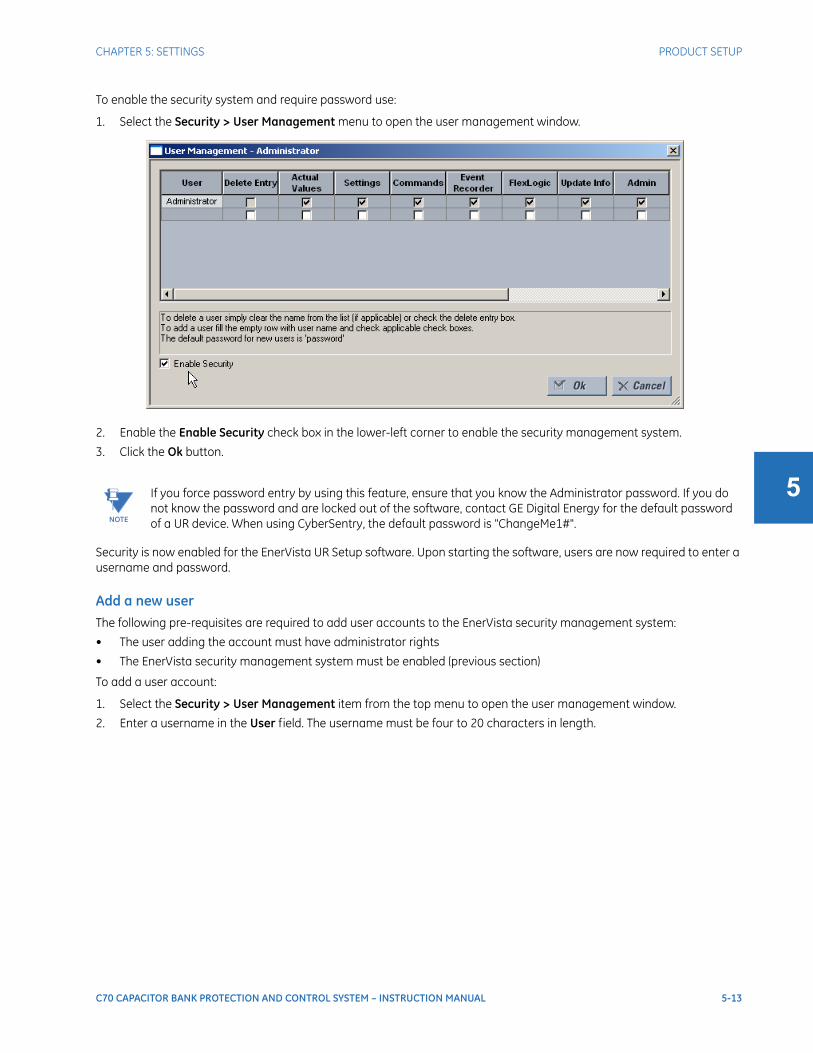
CHAPTER 5: SETTINGS PRODUCT SETUP
C70 CAPACITOR BANK PROTECTION AND CONTROL SYSTEM – INSTRUCTION MANUAL 5-13
5
To enable the security system and require password use:
1. Select the Security > User Management menu to open the user management window.
2. Enable the Enable Security check box in the lower-left corner to enable the security management system.
3. Click the Ok button.
Security is now enabled for the EnerVista UR Setup software. Upon starting the software, users are now required to enter a username and password.
Add a new userThe following pre-requisites are required to add user accounts to the EnerVista security management system:
• The user adding the account must have administrator rights
• The EnerVista security management system must be enabled (previous section)
To add a user account:
1. Select the Security > User Management item from the top menu to open the user management window.
2. Enter a username in the User field. The username must be four to 20 characters in length.
NOTE
If you force password entry by using this feature, ensure that you know the Administrator password. If you do not know the password and are locked out of the software, contact GE Digital Energy for the default password of a UR device. When using CyberSentry, the default password is "ChangeMe1#".
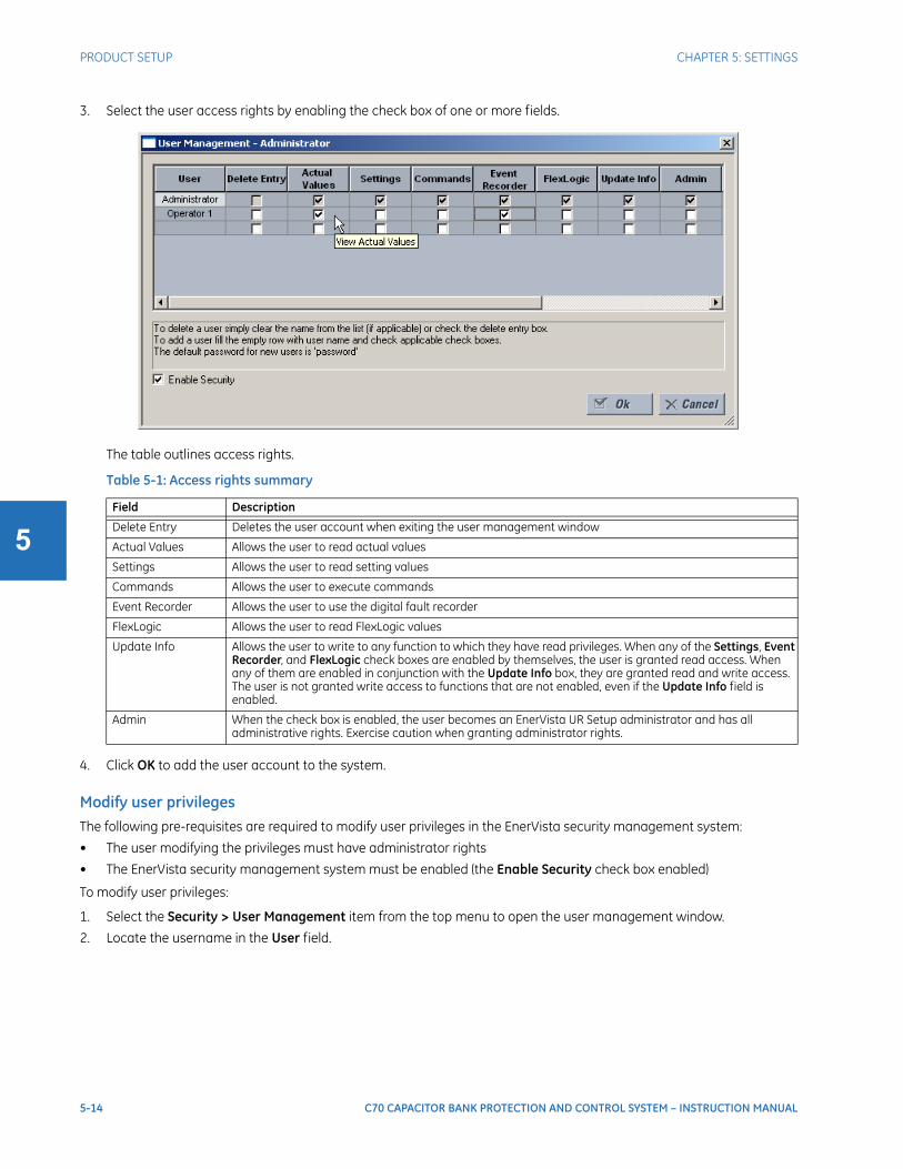
5-14 C70 CAPACITOR BANK PROTECTION AND CONTROL SYSTEM – INSTRUCTION MANUAL
PRODUCT SETUP CHAPTER 5: SETTINGS
5
3. Select the user access rights by enabling the check box of one or more fields.
The table outlines access rights.
Table 5-1: Access rights summary
4. Click OK to add the user account to the system.
Modify user privilegesThe following pre-requisites are required to modify user privileges in the EnerVista security management system:
• The user modifying the privileges must have administrator rights
• The EnerVista security management system must be enabled (the Enable Security check box enabled)
To modify user privileges:
1. Select the Security > User Management item from the top menu to open the user management window.
2. Locate the username in the User field.
Field Description
Delete Entry Deletes the user account when exiting the user management window
Actual Values Allows the user to read actual values
Settings Allows the user to read setting values
Commands Allows the user to execute commands
Event Recorder Allows the user to use the digital fault recorder
FlexLogic Allows the user to read FlexLogic values
Update Info Allows the user to write to any function to which they have read privileges. When any of the Settings, Event Recorder, and FlexLogic check boxes are enabled by themselves, the user is granted read access. When any of them are enabled in conjunction with the Update Info box, they are granted read and write access. The user is not granted write access to functions that are not enabled, even if the Update Info field is enabled.
Admin When the check box is enabled, the user becomes an EnerVista UR Setup administrator and has all administrative rights. Exercise caution when granting administrator rights.
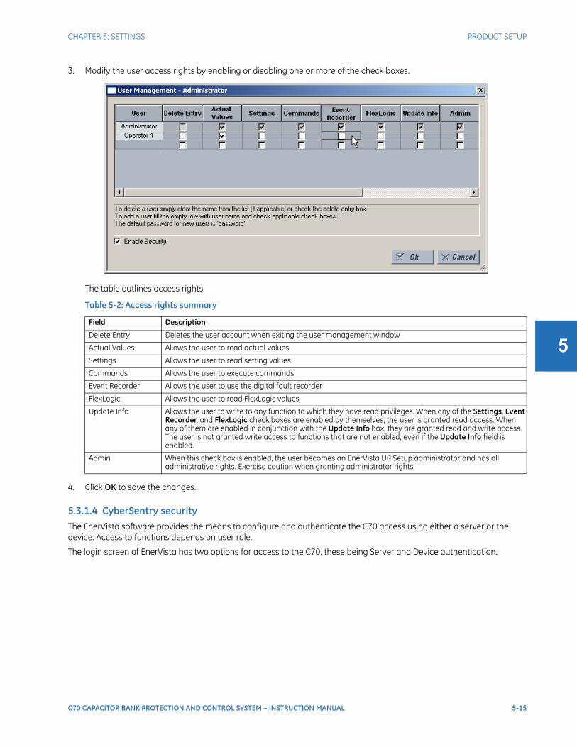
CHAPTER 5: SETTINGS PRODUCT SETUP
C70 CAPACITOR BANK PROTECTION AND CONTROL SYSTEM – INSTRUCTION MANUAL 5-15
5
3. Modify the user access rights by enabling or disabling one or more of the check boxes.
The table outlines access rights.
Table 5-2: Access rights summary
4. Click OK to save the changes.
5.3.1.4 CyberSentry securityThe EnerVista software provides the means to configure and authenticate the C70 access using either a server or the device. Access to functions depends on user role.
The login screen of EnerVista has two options for access to the C70, these being Server and Device authentication.
Field Description
Delete Entry Deletes the user account when exiting the user management window
Actual Values Allows the user to read actual values
Settings Allows the user to read setting values
Commands Allows the user to execute commands
Event Recorder Allows the user to use the digital fault recorder
FlexLogic Allows the user to read FlexLogic values
Update Info Allows the user to write to any function to which they have read privileges. When any of the Settings, Event Recorder, and FlexLogic check boxes are enabled by themselves, the user is granted read access. When any of them are enabled in conjunction with the Update Info box, they are granted read and write access. The user is not granted write access to functions that are not enabled, even if the Update Info field is enabled.
Admin When this check box is enabled, the user becomes an EnerVista UR Setup administrator and has all administrative rights. Exercise caution when granting administrator rights.
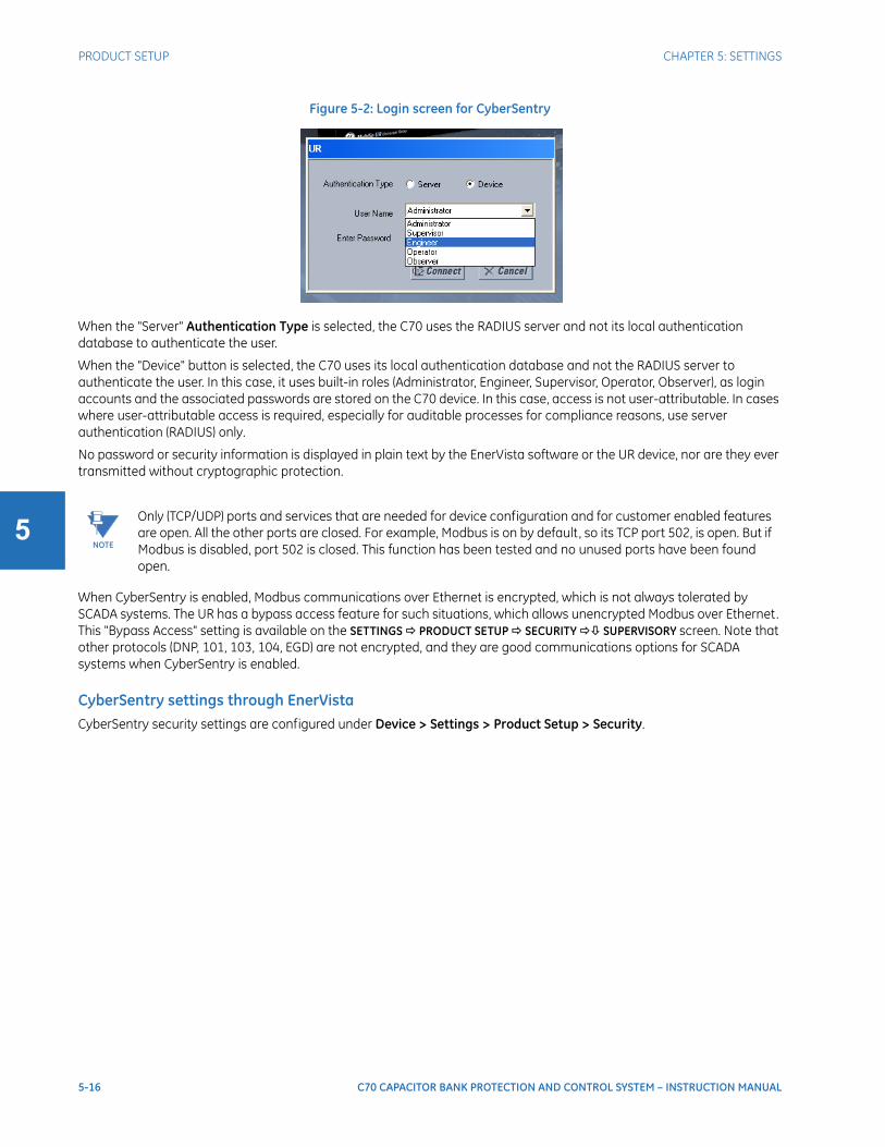
5-16 C70 CAPACITOR BANK PROTECTION AND CONTROL SYSTEM – INSTRUCTION MANUAL
PRODUCT SETUP CHAPTER 5: SETTINGS
5
Figure 5-2: Login screen for CyberSentry
When the "Server" Authentication Type is selected, the C70 uses the RADIUS server and not its local authentication database to authenticate the user.
When the "Device" button is selected, the C70 uses its local authentication database and not the RADIUS server to authenticate the user. In this case, it uses built-in roles (Administrator, Engineer, Supervisor, Operator, Observer), as login accounts and the associated passwords are stored on the C70 device. In this case, access is not user-attributable. In cases where user-attributable access is required, especially for auditable processes for compliance reasons, use server authentication (RADIUS) only.
No password or security information is displayed in plain text by the EnerVista software or the UR device, nor are they ever transmitted without cryptographic protection.
When CyberSentry is enabled, Modbus communications over Ethernet is encrypted, which is not always tolerated by SCADA systems. The UR has a bypass access feature for such situations, which allows unencrypted Modbus over Ethernet. This "Bypass Access" setting is available on the SETTINGS PRODUCT SETUP SECURITY SUPERVISORY screen. Note that other protocols (DNP, 101, 103, 104, EGD) are not encrypted, and they are good communications options for SCADA systems when CyberSentry is enabled.
CyberSentry settings through EnerVistaCyberSentry security settings are configured under Device > Settings > Product Setup > Security.
NOTE
Only (TCP/UDP) ports and services that are needed for device configuration and for customer enabled features are open. All the other ports are closed. For example, Modbus is on by default, so its TCP port 502, is open. But if Modbus is disabled, port 502 is closed. This function has been tested and no unused ports have been found open.
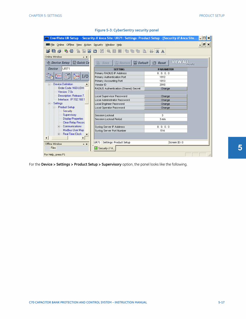
CHAPTER 5: SETTINGS PRODUCT SETUP
C70 CAPACITOR BANK PROTECTION AND CONTROL SYSTEM – INSTRUCTION MANUAL 5-17
5
Figure 5-3: CyberSentry security panel
For the Device > Settings > Product Setup > Supervisory option, the panel looks like the following.
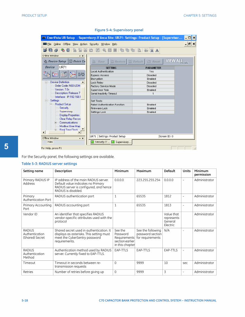
5-18 C70 CAPACITOR BANK PROTECTION AND CONTROL SYSTEM – INSTRUCTION MANUAL
PRODUCT SETUP CHAPTER 5: SETTINGS
5
Figure 5-4: Supervisory panel
For the Security panel, the following settings are available.
Table 5-3: RADIUS server settings
Setting name Description Minimum Maximum Default Units Minimum permission
Primary RADIUS IP Address
IP address of the main RADIUS server. Default value indicates no Primary RADIUS server is configured, and hence RADIUS is disabled.
0.0.0.0 223.255.255.254 0.0.0.0 - Administrator
Primary Authentication Port
RADIUS authentication port 1 65535 1812 - Administrator
Primary Accounting Port
RADIUS accounting port 1 65535 1813 - Administrator
Vendor ID An identifier that specifies RADIUS vendor-specific attributes used with the protocol
Value that represents General Electric
Administrator
RADIUS Authentication (Shared) Secret
Shared secret used in authentication. It displays as asterisks. This setting must meet the CyberSentry password requirements.
See the Password Requirements section earlier in this chapter
See the following password section for requirements
N/A - Administrator
RADIUS Authentication Method
Authentication method used by RADIUS server. Currently fixed to EAP-TTLS.
EAP-TTLS EAP-TTLS EAP-TTLS - Administrator
Timeout Timeout in seconds between re-transmission requests
0 9999 10 sec Administrator
Retries Number of retries before giving up 0 9999 3 - Administrator

CHAPTER 5: SETTINGS PRODUCT SETUP
C70 CAPACITOR BANK PROTECTION AND CONTROL SYSTEM – INSTRUCTION MANUAL 5-19
5
Table 5-4: General security settings
Confirm RADIUS Authentication (Shared) Secret
Confirmation of the shared secret. The entry displays as asterisks.
See the Password Requirements section
245 characters N/A - Administrator
Setting name Description Minimum Maximum Default Units Minimum permission
Session Lockout Number of failed authentications before the device blocks subsequent authentication attempts for the lockout period
0 (lockout disabled)
99 3 - Administrator
Session Lockout Period
The period in minutes that a user is prevented from logging in after being locked out
0 (no period) 9999 3 min Administrator
Syslog Server IP Address
The IP address of the target Syslog server to which all security events are transmitted
0.0.0.0 223.255.255.254
0.0.0.0 - Administrator
Syslog Server Port Number
The UDP port number of the target syslog server to which all security events are transmitted
1 65535 514 - Administrator
Device Authentication
When enabled, local Device authentication with roles is allowed. When disabled, the UR only authenticates to the AAA server (RADIUS).NOTE: Administrator and Supervisor (if still enabled) remain active even after Device authentication is disabled. The only permission for local Administrator is to re-enable Device authentication when Device authentication is disabled. To re-enable Device authentication, the Supervisor unlocks the device for setting changes, and then the Administrator can re-enable Device authentication.
Disabled Enabled Enabled - Administrator
Firmware Lock(via Lock Relay)
Indicates if the device receives firmware upgrades. If Enabled and the firmware upgrade attempt is made, the device denies the upgrade and displays an error message that the lock is set. On each firmware upgrade, this setting goes back to the default .
The Lock Relay setting blocks settings and firmware updates.
Disabled Enabled Enabled - Administrator
Factory Service Mode
When enabled, the device can go into factory service mode. To enable, Supervisor authentication is necessary.
Disabled Enabled Disabled - Supervisor (Administrator when Supervisor is disabled)
Restore to Defaults Sets the device to factory defaults No Yes No - Administrator
Supervisor Role When enabled, the Supervisor role is active. To enable, Administrator authentication is necessary. When disabled, the Supervisor role is inactive. To disable, Supervisor authentication is necessary.
Disabled Enabled Enabled - Administrator to enable and Supervisor to disable
RADIUS user names Ensures that RADIUS user names are not the same as local/device role names
See RADIUS server documents
See RADIUS server documents
- Administrator
Password Local/device roles except for Observer are password-protected. All RADIUS users are password-protected.
See the Password Requirements section earlier in this chapter
See the following password section for requirements
ChangeMe1#
Text The specified role and Administrator, except for Supervisor, where it is only itself
Setting name Description Minimum Maximum Default Units Minimum permission

5-20 C70 CAPACITOR BANK PROTECTION AND CONTROL SYSTEM – INSTRUCTION MANUAL
PRODUCT SETUP CHAPTER 5: SETTINGS
5
Table 5-5: Security alarm settings
CyberSentry settings through the front panelSETTINGS PRODUCT SETUP SECURITY
LOGIN — This setting is applicable for Device authentication only. This setting allows a user to log in with a specific role, as outlined here. For the Supervisor role, enable the “Supervisor Role” setting.
Whenever a new role is logged in, the user is prompted to enter a password. Passwords must obey the requirements specified earlier in the chapter in the Password Requirements section.The UR device supports five roles. Roles have their corresponding passwords, except the Observer role, which does not require a password.
The roles are defined as follows:
• Administrator — Complete read/write access to all settings and commands. This role does not allow concurrent access. This role has an operand to indicate when it is logged on.
• Engineer — Complete read/write access to all settings and commands except configuring Security settings and firmware upgrades. This role does not allow concurrent access.
• Operator — The Operator has read/write access to all settings under the Commands menu/section. This role does not exist offline.
• Supervisor — This is only an approving role. This role’s authentication commits setting changes submitted by Administrator or Engineer. The Supervisor role authenticates to unlock the UR relay for setting changes and not approve changes after the fact. Only a Supervisor can set the Settings Lock and Firmware Lock in the Security settings. This role also has the ability to forcefully log off any other role and clear the security event log. This role can also be disabled, but only through a Supervisor authentication. When this role is disabled its permissions are assigned to the Administrator role.
Setting name Description / Details Min Max Default Units Minimum permissions
Failed Authentications
A threshold number indicating when an alarm is set off to indicate too many failed authentication attempts
0 (disabled)
99 3 - Administrator
Firmware Lock A value indicating if the device can receive a firmware upgrade. If Enabled and a firmware upgrade attempt is made, the device alarm activates. If Disabled, the device alarm does not activate. On each firmware upgrade this setting goes back to the default.
Disabled Enabled Enabled - Administrator
Settings Lock A value indicating if the device can accept any settings changes. If Enabled and a settings change attempt is made, the device alarm activates. If Disabled, the device alarm does not activate.
Disabled Enabled Enabled - Supervisor (Administrator if Supervisor has been disabled)
SECURITY LOGIN:
NoneRange: Administrator, Engineer, Supervisor,Operator, Factory (for factory use only), None
CHANGE LOCAL PASSWORDS
See page 5-21
SESSION SETTINGS
See page 5-21
RESTORE DEFAULTS
See page 5-21
SUPERVISORY
See page 5-22
SYSLOG IP ADDRESS:0.0.0.0
Range: 0.0.0.0, 255.255.255.255
SYSLOG PORT NUMBER:514
Range: 1 to 65535

CHAPTER 5: SETTINGS PRODUCT SETUP
C70 CAPACITOR BANK PROTECTION AND CONTROL SYSTEM – INSTRUCTION MANUAL 5-21
5
• Observer — This role has read-only access to all C70 settings. This role allows unlimited concurrent access but it has no download access to any files on the device. Observer is the default role if no authentication has been done to the device. This role displays as "None" on the front panel.
Change local passwordsSETTINGS PRODUCT SETUP SECURITY CHANGE LOCAL PASSWORDS
The Change Local Passwords menu is shown on the front panel and in EnerVista upon successful login of the Administrator role.
The LOGIN setting in this menu is similar to that described in SETTINGS > PRODUCT SETUP > SECURITY except for the factory role.
Passwords are stored in text format. No encryption is applied.
Session settingsSETTINGS PRODUCT SETUP SECURITY SESSION SETTINGS
SESSION LOCKOUT — This setting specifies the number of failed authentications before the device blocks subsequent authentication attempts for the lockout period. A value of zero means lockout is disabled.
SESSION LOCKOUT PERIOD — This setting specifies the period of time in minutes of a lockout period. A value of 0 means that there is no lockout period.
Restore defaultsSETTINGS PRODUCT SETUP SECURITY RESTORE DEFAULTS
NOTE
The Factory service role is not available. It is for factory use only.
CHANGE LOCAL PASSWORDS LOGIN:
NoneRange: 20 alphanumeric characters
NEW PASSWORD: Range: 20 alphanumeric characters
CONFIRM PASSWORD: Range: 20 alphanumeric characters
NOTE
In Device authentication mode, the Observer role does not have a password associated with it . In Server authentication mode the Observer role requires a password.If you are locked out of the software, contact GE Digital Energy for the default password. When using CyberSentry, the default password is "ChangeMe1#".Once the passwords are set, the Administrator with Supervisor approval can change the role-associated password.In CyberSentry, password encryption is not supported.
SESSION SETTINGS SESSION LOCKOUT:
3Range: 0 to 99
SESSION LOCKOUTPERIOD: 3 min
Range: 0 to 9999 minutes
RESTORE DEFAULTS LOAD FACTORY
DEFAULTS: NoRange: Yes, No

5-22 C70 CAPACITOR BANK PROTECTION AND CONTROL SYSTEM – INSTRUCTION MANUAL
PRODUCT SETUP CHAPTER 5: SETTINGS
5
LOAD FACTORY DEFAULTS — This setting is used to reset all the settings, communication, and security passwords. An Administrator role is used to change this setting and a Supervisor role (if not disabled) approves it .
SupervisorySETTINGS PRODUCT SETUP SECURITY SUPERVISORY
The Supervisory menu settings are available for Supervisor role only, or if the Supervisor role is disabled then for the Administrator role only.
DEVICE AUTHENTICATION — This setting is enabled by default, meaning "Yes" is selected. When enabled, Device authentication with roles is enabled. When this setting is disabled, the UR only authenticates to the AAA server (RADIUS). However, the Administrator and Supervisor (when enabled) remain active even after device authentication is disabled and their only permission is to re-enable Device authentication. To re-enable Device authentication, the Supervisor unlocks the device for settings changes, then the Administrator re-enables device authentication.
BYPASS ACCESS — The bypass security feature provides an easier access, with no authentication and encryption for those special situations when this is considered safe. Only the Supervisor, or the Administrator when the Supervisor role is disabled, can enable this feature.
The bypass options are as follows:
• Local — Bypasses authentication for push buttons, keypad, RS232, and RS485
• Remote — Bypasses authentication for Ethernet
• Local and Remote — Bypasses authentication for push buttons, keypad, RS232, RS485, and Ethernet
When CyberSentry is enabled, Modbus communications over Ethernet is encrypted, which is not always tolerated by SCADA systems. The UR has the Bypass Access feature for such situations, which allows unencrypted Modbus over Ethernet. Setting it to "Remote" ensures no authentication is required over Ethernet and Modbus communication is unencrypted. Only a Supervisor or Administrator (if Supervisor role is disabled) can enable this feature. Note that other protocols (DNP, 101, 103, 104, EGD) are not encrypted, and they are good communications options for SCADA systems when CyberSentry is enabled.
LOCK RELAY — This setting uses a Boolean value (Enabled/Disabled) to indicate if the device accepts settings changes and whether the device can receive a firmware upgrade. This setting can be changed by the Supervisor role, if it is enabled, or by the Administrator if the Supervisor role is disabled. The Supervisor role disables this setting for the relay to start accepting settings changes, command changes, or firmware upgrade. After all the setting changes are applied or commands executed, the Supervisor enables to lock settings changes.
SUPERVISORY DEVICE
AUTHENTICATION: YesRange: Yes, No
BYPASS ACCESS:Disabled
Range: Local, Remote, Local and Remote, Disabled
LOCK RELAY:Disabled
Range: Enabled, Disabled
FACTORY SERVICEMODE: Disabled
Range: Enabled, Disabled
SELF TESTS
See below
SUPERVISOR ROLE:Disabled
Range: Enabled, Disabled
SERIAL INACTIVITYTIMEOUT: 1 min
Range: 1 to 9999 minutes
Mode Front panel or serial (RS232, RS485) Ethernet
Normal mode Authentication — Role Based Access Control (RBAC)and passwords in clear
Authentication — RBAC and passwords encryptedSSH tunneling
Bypass access mode No passwords for allowed RBAC levels No passwords for allowed RBAC levelsNo SSH tunneling

CHAPTER 5: SETTINGS PRODUCT SETUP
C70 CAPACITOR BANK PROTECTION AND CONTROL SYSTEM – INSTRUCTION MANUAL 5-23
5
Example: If this setting is enabled and an attempt is made to change settings or upgrade the firmware, the UR device denies the settings changes or denies upgrading the firmware. If this setting is disabled, the UR device accepts settings changes and firmware upgrade.
This role is disabled by default.
FACTORY SERVICE MODE — When Enabled, the device can go into factory service mode. For this setting to become enabled a Supervisor authentication is necessary. The default value is Disabled.
SUPERVISOR ROLE — When Enabled, the Supervisor role is active. To Disable this setting a Supervisor authentication is necessary. If disabled, the Supervisor role is not allowed to log in. In this case, the Administrator can change the settings under the Supervisory menu.
If enabled, Supervisor authentication is required to change the settings in the Supervisory menu. If the Supervisor disables their role after authentication, the Supervisor session remains valid until they switch to another role using MMI or until they end the current Supervisor session if using communications.
This role is disabled by default.
SERIAL INACTIVITY TIMEOUT — The role logged via a serial port is auto logged off after the Serial Inactivity timer times out. A separate timer is maintained for RS232 and RS485 connections. The default value is 1 minute.
Self-tests
SETTINGS PRODUCT SETUP SECURITY SUPERVISORY SELF TESTS
FAILED AUTHENTICATE — If this setting is Enabled then the number of failed authentications is compared with the Session Lockout threshold. When the Session Lockout threshold is exceeded, this minor alarm indication comes up.
FIRMWARE LOCK — If this setting is Enabled, then any firmware upgrade operation attempt when the Lock Relay setting is enabled brings up this self test alarm.
SETTINGS LOCK — If this setting is Enabled then an unauthorized write attempt to a setting for a given role activates this self test.
SETTINGS PRODUCT SETUP SECURITY SUPERVISORY SELF TESTS FAILED AUTHENTICATE
CyberSentry setupWhen first using CyberSentry security, use the following procedure for setup.
1. Log in to the relay as Administrator by using the VALUE keys on the front panel to enter the default password "ChangeMe1#". Note that the Lock Relay setting needs to be disabled in the Security > Supervisory menu. When this setting is disabled, configuration and firmware upgrade are possible. By default, this setting is disabled.
2. Enable the Supervisor role if you have a need for it .
3. Make any required changes in configuration, such as setting a valid IP address for communication over Ethernet.
4. Log out of the Administrator account by choosing None.
5. Next, Device or Server authentication can be chosen on the login screen, but the choice is available only in EnerVista. Use Device authentication to log in using the five pre-configured roles (Administrator, Supervisor, Engineer, Operator, Observer). When using a serial connection, only Device authentication is supported. When Server authentication is required, characteristics for communication with a RADIUS server must be configured. This is possible only in the EnerVista software. The RADIUS server itself also must be configured. The appendix called RADIUS Server at the end of this instruction manual gives an example of how to set up a simple RADIUS server. Once both the RADIUS server and
SELF TESTS FAILED
AUTHENTICATESee below
FIRMWARE LOCK:Enabled
Range: Enabled, Disabled
SETTINGS LOCK:Enabled
Range: Enabled, Disabled
FAILED AUTHENTICATE FAILED AUTHENTICATE:
EnabledRange: Enabled, Disabled
5-24 C70 CAPACITOR BANK PROTECTION AND CONTROL SYSTEM – INSTRUCTION MANUAL
PRODUCT SETUP CHAPTER 5: SETTINGS
5
the parameters for connecting the UR to the server have been configured, you can choose Server authentication on the login screen of EnerVista.
To configure Server authentication:
1. In the EnerVista software, choose Device authentication and log in as Administrator.
2. Configure the following RADIUS server parameters: IP address, authentication port, shared secret, and vendor ID.
3. On the RADIUS server, configure the user accounts. Do not use the five pre-defined roles as user names (Administrator, Supervisor, Engineer, Operator, Observer) in the RADIUS server. If you do, the UR relay automatically provides the authentication from the device.
4. In the EnerVista software, choose Server authentication and log in using the user name and password configured on the RADIUS server for Server authentication login.
5. After making any required changes, log out.
Pushbuttons (both user-control buttons and user-programmable buttons) located on the front panel can be pressed by an Administrator or Engineer role. This also applies to the RESET button, which resets targets, where targets are errors displayed on the front panel or the Targets panel of the EnerVista software. The RESET button has special behavior in that it allows these two roles to press it even when they are logged in through the RS232 port and not through the front panel.
To reset the security event log and self-test operands:
1. Log in as Supervisor (if the role is enabled) or Administrator (if the Supervisor role is disabled) and execute a clear security command under Commands > Security > Clear Security.
Syslog formatSystem logs are produced with the CyberSentry option. The format is as follows.
Event Number — Event identification number (index)
Date & Timestamp — UTC date and time
Username — 255 chars maximum, but in the security log it is truncated to 20 characters
IP address — Device IP address
The use of CyberSentry for devices communicating through an Ethernet-to-RS485 gateway is not supported. Because these gateways do not support the secure protocols necessary to communicate with such devices, the connection cannot be established. Use the device as a non-CyberSentry device.
Users logged in through the front panel are not timed out and cannot be forcefully logged out by a supervisor. Roles logged in through the front panel that do no allow multiple instances (Administrator, Supervisor, Engineer, Operator) must switch to None (equivalent to a logout) when they are done in order to log out.
For all user roles except Observer, only one instance can be logged in at a time, for both login by front panel and software.
When changing settings offline, ensure that only settings permitted by the role that performs the settings download are changed because only those changes are applied.
Security log Event Number Date & Timestamp
Username IP address Role Activity Value

CHAPTER 5: SETTINGS PRODUCT SETUP
C70 CAPACITOR BANK PROTECTION AND CONTROL SYSTEM – INSTRUCTION MANUAL 5-25
5
Role — 16 bit unsigned, of type format F617
Activity Value — 16 bit unsigned
5.3.2 Display propertiesSETTINGS PRODUCT SETUP DISPLAY PROPERTIES
Enumeration Role
0 None
1 Administrator
2 Supervisor
3 Engineer
4 Operator
5 Factory
Enumeration Description
1 Authentication Failed
2 User Lockout
3 FW Upgrade
4 FW Lock
5 Settings Lock
6 Settings Change. Because this can fill the entire event log, it is supported by the already existing Settings_Change.log file. This event is not required.
7 Clear Oscillography command
8 Clear Data Logger command (not applicable to all UR products)
9 Clear Demand Records command (not applicable to all UR products)
10 Clear Energy command (not applicable to all UR products)
11 Clear Unauthorized Access command
12 Clear Teleprotection Counters command (not applicable to all UR products)
13 Clear All Relay Records command
14 Role Log in
15 Role Log off
DISPLAY PROPERTIES
LANGUAGE:English
Range: English; English, French; English, Russian; English, Chinese; English, German (examples; depends on order code)Visible when language other than English purchased
FLASH MESSAGETIME: 1.0 s
Range: 0.5 to 10.0 s in steps of 0.1
DEFAULT MESSAGETIMEOUT: 300 s
Range: 10 to 900 s in steps of 1
DEFAULT MESSAGEINTENSITY: 25 %
Range: 25%, 50%, 75%, 100%Visible when a VFD is installed
SCREEN SAVERFEATURE: Disabled
Range: Disabled, EnabledVisible when an LCD is installed
SCREEN SAVER WAITTIME: 30 min
Range: 1 to 65535 min. in steps of 1Visible when an LCD is installed
CURRENT CUT-OFFLEVEL: 0.020 pu
Range: 0.002 to 0.020 pu in steps of 0.001
VOLTAGE CUT-OFFLEVEL: 1.0 V
Range: 0.1 to 1.0 V secondary in steps of 0.1

5-26 C70 CAPACITOR BANK PROTECTION AND CONTROL SYSTEM – INSTRUCTION MANUAL
PRODUCT SETUP CHAPTER 5: SETTINGS
5
Some relay messaging characteristics can be modified to suit different situations using the display properties settings.
LANGUAGE — This setting selects the language used to display settings, actual values, and targets. This setting displays when a language other than English was purchased, and the range depends on the order code of the relay.
FLASH MESSAGE TIME — Flash messages are status, warning, error, and information messages displayed in response to certain key presses during settings programming. These messages override any normal messages. Use this setting to change the duration of flash messages on the display.
DEFAULT MESSAGE TIMEOUT — If the keypad is inactive for a period of time, the relay automatically reverts to a default message. The inactivity time is modified using this setting to ensure that messages remain on the screen long enough during programming or reading of actual values.
DEFAULT MESSAGE INTENSITY — To extend phosphor life in the vacuum fluorescent display, the brightness can be attenuated during default message display. During keypad interrogation, the display always operates at full brightness.
SCREEN SAVER FEATURE and SCREEN SAVER WAIT TIME — These settings are only visible if the C70 has a liquid crystal display (LCD) and control its backlighting. When the SCREEN SAVER FEATURE is “Enabled,” the LCD backlighting turns off after the DEFAULT MESSAGE TIMEOUT followed by the SCREEN SAVER WAIT TIME, provided that no keys have been pressed and no target messages are active. When a keypress occurs or a target becomes active, the LCD backlighting turns on.
CURRENT CUT-OFF LEVEL — This setting modifies the current cut-off threshold. Very low currents (1 to 2% of the rated value) are very susceptible to noise. Some customers prefer very low currents to display as zero, while others prefer the current to display even when the value reflects noise rather than the actual signal. The C70 applies a cut-off value to the magnitudes and angles of the measured currents. If the magnitude is below the cut-off level, it is substituted with zero. This applies to phase and ground current phasors as well as true RMS values and symmetrical components. The cut-off operation applies to quantities used for metering, protection, and control, as well as those used by communications protocols. Note that the cut-off level for the sensitive ground input is 10 times lower that the CURRENT CUT-OFF LEVEL setting value. Raw current samples available via oscillography are not subject to cut-off.
VOLTAGE CUT-OFF LEVEL — This setting modifies the voltage cut-off threshold. Very low secondary voltage measurements (at the fractional volt level) can be affected by noise. Some customers prefer these low voltages to be displayed as zero, while others prefer the voltage to be displayed even when the value reflects noise rather than the actual signal. The C70 applies a cut-off value to the magnitudes and angles of the measured voltages. If the magnitude is below the cut-off level, it is substituted with zero. This operation applies to phase and auxiliary voltages, and symmetrical components. The cut-off operation applies to quantities used for metering, protection, and control, as well as those used by communications protocols. Raw samples of the voltages available via oscillography are not subject to cut-off.
The CURRENT CUT-OFF LEVEL and the VOLTAGE CUT-OFF LEVEL are used to determine the metered power cut-off levels. The power cut-off level is calculated using the following equations. For Delta connections:
Eq. 5-3
For Wye connections:
Eq. 5-4
Eq. 5-5
where VT primary = VT secondary × VT ratio and CT primary = CT secondary × CT ratio.
For example, given the following settings:CURRENT CUT-OFF LEVEL: “0.02 pu”VOLTAGE CUT-OFF LEVEL: “1.0 V”PHASE CT PRIMARY: “100 A”PHASE VT SECONDARY: “66.4 V”PHASE VT RATIO: “208.00 : 1"PHASE VT CONNECTION: “Delta”
We have:CT primary = “100 A”, andVT primary = PHASE VT SECONDARY x PHASE VT RATIO = 66.4 V x 208 = 13811.2 V
3-phase power cut-off 3 CURRENT CUT-OFF LEVEL VOLTAGE CUT-OFF LEVEL VT primary CT primary××××VT secondary
--------------------------------------------------------------------------------------------------------------------------------------------------------------------------------------=
3-phase power cut-off 3 CURRENT CUT-OFF LEVEL VOLTAGE CUT-OFF LEVEL VT primary CT primary××××VT secondary
----------------------------------------------------------------------------------------------------------------------------------------------------------------------------------=
per-phase power cut-off CURRENT CUT-OFF LEVEL VOLTAGE CUT-OFF LEVEL VT primary CT primary×××VT secondary
--------------------------------------------------------------------------------------------------------------------------------------------------------------------------=
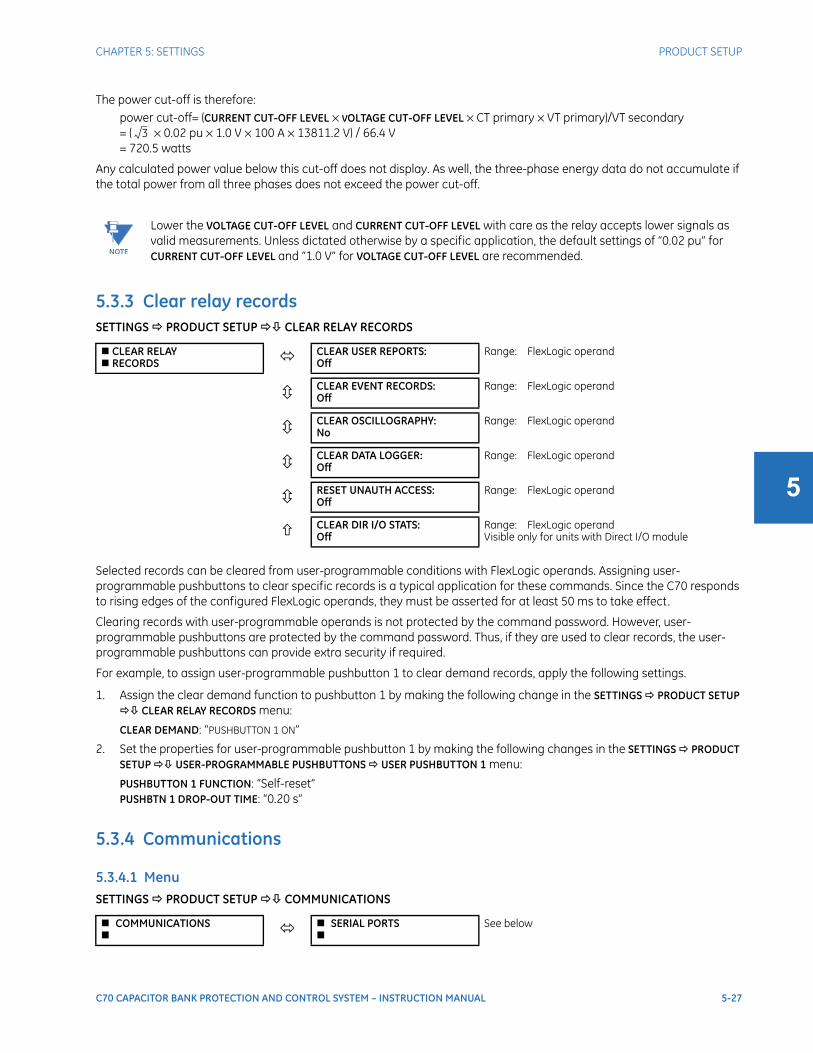
CHAPTER 5: SETTINGS PRODUCT SETUP
C70 CAPACITOR BANK PROTECTION AND CONTROL SYSTEM – INSTRUCTION MANUAL 5-27
5
The power cut-off is therefore:power cut-off= (CURRENT CUT-OFF LEVEL × VOLTAGE CUT-OFF LEVEL × CT primary × VT primary)/VT secondary= ( × 0.02 pu × 1.0 V × 100 A × 13811.2 V) / 66.4 V = 720.5 watts
Any calculated power value below this cut-off does not display. As well, the three-phase energy data do not accumulate if the total power from all three phases does not exceed the power cut-off.
5.3.3 Clear relay recordsSETTINGS PRODUCT SETUP CLEAR RELAY RECORDS
Selected records can be cleared from user-programmable conditions with FlexLogic operands. Assigning user-programmable pushbuttons to clear specific records is a typical application for these commands. Since the C70 responds to rising edges of the configured FlexLogic operands, they must be asserted for at least 50 ms to take effect.
Clearing records with user-programmable operands is not protected by the command password. However, user-programmable pushbuttons are protected by the command password. Thus, if they are used to clear records, the user-programmable pushbuttons can provide extra security if required.
For example, to assign user-programmable pushbutton 1 to clear demand records, apply the following settings.
1. Assign the clear demand function to pushbutton 1 by making the following change in the SETTINGS PRODUCT SETUP CLEAR RELAY RECORDS menu:
CLEAR DEMAND: “PUSHBUTTON 1 ON”
2. Set the properties for user-programmable pushbutton 1 by making the following changes in the SETTINGS PRODUCT SETUP USER-PROGRAMMABLE PUSHBUTTONS USER PUSHBUTTON 1 menu:
PUSHBUTTON 1 FUNCTION: “Self-reset”PUSHBTN 1 DROP-OUT TIME: “0.20 s”
5.3.4 Communications
5.3.4.1 MenuSETTINGS PRODUCT SETUP COMMUNICATIONS
NOTE
Lower the VOLTAGE CUT-OFF LEVEL and CURRENT CUT-OFF LEVEL with care as the relay accepts lower signals as valid measurements. Unless dictated otherwise by a specific application, the default settings of “0.02 pu” for CURRENT CUT-OFF LEVEL and “1.0 V” for VOLTAGE CUT-OFF LEVEL are recommended.
CLEAR RELAY RECORDS CLEAR USER REPORTS:
OffRange: FlexLogic operand
CLEAR EVENT RECORDS:Off
Range: FlexLogic operand
CLEAR OSCILLOGRAPHY:No
Range: FlexLogic operand
CLEAR DATA LOGGER:Off
Range: FlexLogic operand
RESET UNAUTH ACCESS:Off
Range: FlexLogic operand
CLEAR DIR I/O STATS:Off
Range: FlexLogic operandVisible only for units with Direct I/O module
COMMUNICATIONS SERIAL PORTS
See below
3
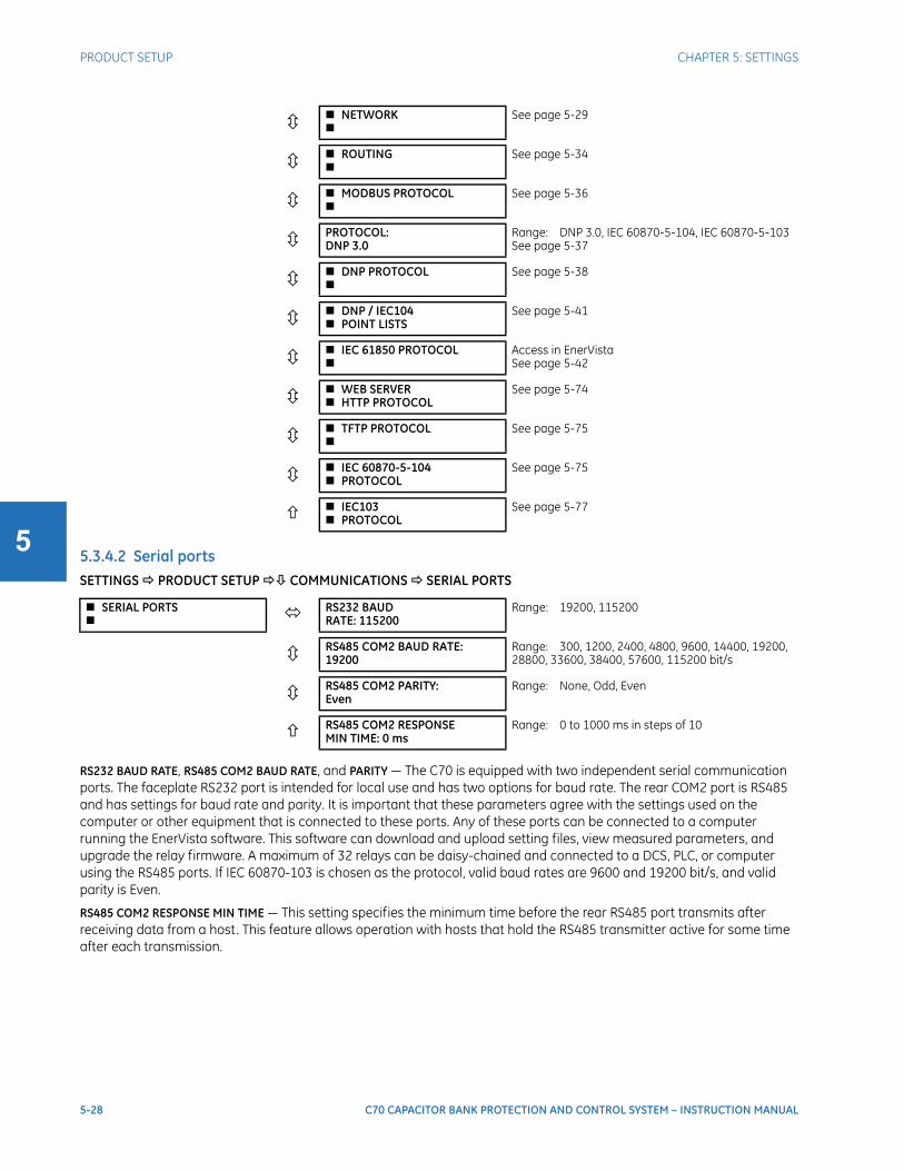
5-28 C70 CAPACITOR BANK PROTECTION AND CONTROL SYSTEM – INSTRUCTION MANUAL
PRODUCT SETUP CHAPTER 5: SETTINGS
55.3.4.2 Serial portsSETTINGS PRODUCT SETUP COMMUNICATIONS SERIAL PORTS
RS232 BAUD RATE, RS485 COM2 BAUD RATE, and PARITY — The C70 is equipped with two independent serial communication ports. The faceplate RS232 port is intended for local use and has two options for baud rate. The rear COM2 port is RS485 and has settings for baud rate and parity. It is important that these parameters agree with the settings used on the computer or other equipment that is connected to these ports. Any of these ports can be connected to a computer running the EnerVista software. This software can download and upload setting files, view measured parameters, and upgrade the relay firmware. A maximum of 32 relays can be daisy-chained and connected to a DCS, PLC, or computer using the RS485 ports. If IEC 60870-103 is chosen as the protocol, valid baud rates are 9600 and 19200 bit/s, and valid parity is Even.
RS485 COM2 RESPONSE MIN TIME — This setting specifies the minimum time before the rear RS485 port transmits after receiving data from a host. This feature allows operation with hosts that hold the RS485 transmitter active for some time after each transmission.
NETWORK
See page 5-29
ROUTING
See page 5-34
MODBUS PROTOCOL
See page 5-36
PROTOCOL:DNP 3.0
Range: DNP 3.0, IEC 60870-5-104, IEC 60870-5-103See page 5-37
DNP PROTOCOL
See page 5-38
DNP / IEC104 POINT LISTS
See page 5-41
IEC 61850 PROTOCOL
Access in EnerVistaSee page 5-42
WEB SERVER HTTP PROTOCOL
See page 5-74
TFTP PROTOCOL
See page 5-75
IEC 60870-5-104 PROTOCOL
See page 5-75
IEC103 PROTOCOL
See page 5-77
SERIAL PORTS RS232 BAUD
RATE: 115200Range: 19200, 115200
RS485 COM2 BAUD RATE:19200
Range: 300, 1200, 2400, 4800, 9600, 14400, 19200, 28800, 33600, 38400, 57600, 115200 bit/s
RS485 COM2 PARITY:Even
Range: None, Odd, Even
RS485 COM2 RESPONSEMIN TIME: 0 ms
Range: 0 to 1000 ms in steps of 10

CHAPTER 5: SETTINGS PRODUCT SETUP
C70 CAPACITOR BANK PROTECTION AND CONTROL SYSTEM – INSTRUCTION MANUAL 5-29
5
5.3.4.3 Ethernet network topologyThe C70 has three Ethernet ports. Each Ethernet port must belong to a different network or subnetwork. Configure the IP address and subnet to ensure that each port meets this requirement. Two subnets are different when the bitwise AND operation performed between their respective IP address and mask produces a different result. Communication becomes unpredictable when more than one port is configured to the same subnet.
Example 1IP1/Mask1: 10.1.1.2/255.255.255.0 (where LAN 1 is 10.1.1.x/255.255.255.0)
IP2/Mask2: 10.2.1.2/255.255.255.0 (where LAN2 is 10.2.1.x/255.255.255.0)
IP3/Mask3: 10.3.1.2/255.255.255.0 (where LAN3 is 10.3.1.x/255.255.255.0)
Example 2IP1/Mask1: 10.1.1.2/255.0.0.0 (where LAN1 is 10.x.x.x/255.0.0.0)
IP2/Mask2: 11.1.1.2/255.0.0.0 (where LAN2 is 11.x.x.x/255.0.0.0)
IP3/Mask3: 12.1.1.2/255.0.0.0 (where LAN3 is 12.x.x.x/255.0.0.0)
Example 3 — IncorrectIP1/Mask1: 10.1.1.2/255.0.0.0
IP2/Mask2: 10.2.1.2/255.0.0.0
IP3/Mask3: 10.3.1.2/255.0.0.0
This example is incorrect because the mask of 255.0.0.0 used for the three IP addresses makes them belong to the same network of 10.x.x.x.
Single LAN, no redundancyThe topology shown in the following figure allows communications to SCADA, local configuration/monitoring through EnerVista, and access to the public network shared on the same LAN. No redundancy is provided.
Figure 5-5: Network configuration for single LAN
EnerVista Software
ML3000
Public Network
SCADA
UR
P2 P3
LAN1
P1IP1/
MAC1
859708A2.vsd
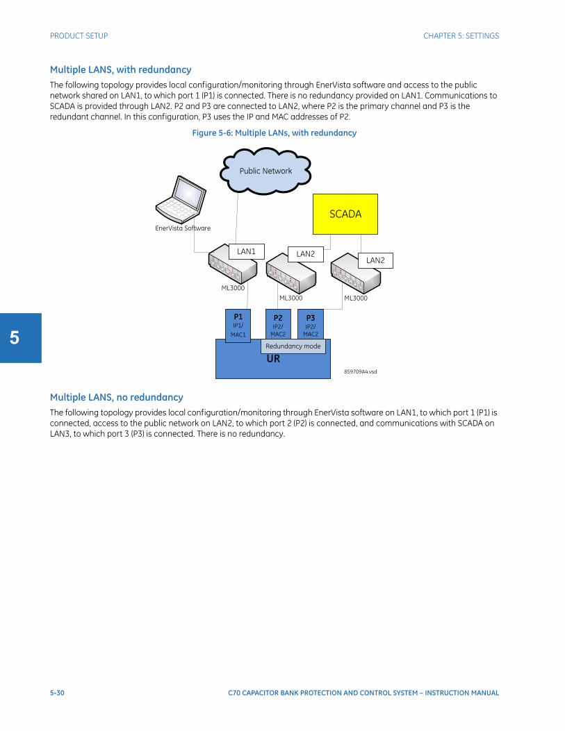
5-30 C70 CAPACITOR BANK PROTECTION AND CONTROL SYSTEM – INSTRUCTION MANUAL
PRODUCT SETUP CHAPTER 5: SETTINGS
5
Multiple LANS, with redundancyThe following topology provides local configuration/monitoring through EnerVista software and access to the public network shared on LAN1, to which port 1 (P1) is connected. There is no redundancy provided on LAN1. Communications to SCADA is provided through LAN2. P2 and P3 are connected to LAN2, where P2 is the primary channel and P3 is the redundant channel. In this configuration, P3 uses the IP and MAC addresses of P2.
Figure 5-6: Multiple LANs, with redundancy
Multiple LANS, no redundancyThe following topology provides local configuration/monitoring through EnerVista software on LAN1, to which port 1 (P1) is connected, access to the public network on LAN2, to which port 2 (P2) is connected, and communications with SCADA on LAN3, to which port 3 (P3) is connected. There is no redundancy.
P3 IP2/
MAC2
EnerVista Software
ML3000
Public Network
SCADA
UR
P1 IP1/
MAC1
P2 IP2/
MAC2
ML3000 ML3000
Redundancy mode
LAN1 LAN2LAN2
859709A4.vsd

CHAPTER 5: SETTINGS PRODUCT SETUP
C70 CAPACITOR BANK PROTECTION AND CONTROL SYSTEM – INSTRUCTION MANUAL 5-31
5
Figure 5-7: Multiple LANS, no redundancy
5.3.4.4 NetworkAs outlined in the previous section, when using more than one Ethernet port, configure each to belong to a different network or subnet using the IP addresses and mask. Configure the network IP and subnet settings before configuring the routing settings.
SETTINGS PRODUCT SETUP COMMUNICATIONS NETWORK 1(3)
The IP addresses are used with the DNP, Modbus/TCP, IEC 61580, IEC 60870-5-104, TFTP, HTTP, and PRP protocols. PRP is explained in its own section later.
PRT1 (2 or 3) IP ADDRESS — This setting sets the port’s IPv4 address in standard IPV4 format. This setting is valid on port 3 if port 2 REDUNDANCY is set to None.
NETWORK PORT 1 PRT1 IP ADDRESS:
127.0.0.1Range: standard IPV4 address format
PRT1 SUBNET IP MASK:255.0.0.0
Range: standard IPV4 address format
NETWORK PORT 2 PRT2 IP ADDRESS:
127.0.0.1Range: standard IPV4 address format
PRT2 SUBNET IP MASK:255.0.0.0
Range: standard IPV4 address format
PRT2 REDUNDANCY:None
Range: None, Failover, PRPRange if no PRP license: None, Failover
PRT2 PRP MCST ADDR:01-15-4E-00-01-00
Range: 01-15-4E-00-01-00 to 01-15-4E-00-01-FF
NETWORK PORT 3 PRT3 IP ADDRESS:
127.0.0.1Range: standard IPV4 address format
PRT3 SUBNET IP MASK:255.0.0.0
Range: standard IPV4 address format
EnerVista Software
ML3000
Public Network
SCADA
UR
P1IP1/
MAC1
P2 IP2/
MAC2
ML3000 ML3000
LAN1 LAN2LAN3
P3 IP3/
MAC3
859710A2.vsd

5-32 C70 CAPACITOR BANK PROTECTION AND CONTROL SYSTEM – INSTRUCTION MANUAL
PRODUCT SETUP CHAPTER 5: SETTINGS
5
PRT1 (2 or 3) SUBNET MASK — This setting sets the port’s IPv4 subnet mask in standard IPV4 format. This setting is valid on port 3 if port 2 REDUNDANCY is set to None.
PRT2 REDUNDANCY — Determines if ports 2 and 3 operate in redundant or independent mode. If a license for PRP was purchased, the options are None, Failover, and PRP. If a license for PRP was not purchased, the options are None and Failover. In non-redundant mode (REDUNDANCY set to None), ports 2 and 3 operate independently with their own MAC, IP, and mask addresses. If REDUNDANCY is set to Failover, the operation of ports 2 and 3 is as follows:
• Ports 2 and 3 use the port 2 MAC address, IP address, and mask
• The configuration fields for IP address and mask on port 3 are hidden
• Port 3 is in standby mode and does not actively communicate on the Ethernet network but monitors its link to the Multilink switch. If port 2 detects a problem with the link, communications is switched to Port 3. Port 3 is, in effect, acting as a redundant or backup link to the network for port 2. Once port 2 detects that the link between itself and the switch is good and that communication is healthy for five minutes, then switching back to port 2 is performed. The delay in switching back ensures that rebooted switching devices connected to the C70, which signal their ports as active prior to being completely functional, have time to completely initialize themselves and become active. Once port 2 is active again, port 3 returns to standby mode.
If REDUNDANCY is set to PRP, the operation of ports 2 and 3 is as follows:
• Ports 2 and 3 use the port 2 MAC address, IP address, and mask
• The configuration fields for IP address and mask on port 3 are overwritten with those from port 2. This is visible on the front panel but not displayed in the EnerVista software.
• Port 2 MCST ADDRESS field is visible
• The port 2 PTP function still uses only port 2 and the port 3 PTP function still uses only port 3. The relay still synchronizes to whichever port has the best master. When ports 2 and 3 see the same master, as is typically the case for PRP networks, the port with the better connectivity is used.
For any changes to this setting to take effect, restart the unit.
PRT2 PRP MCST ADDR — This setting allows the user to change the multicast address used by the PRP supervision frames. This setting is available if REDUNDANCY is set to PRP. All devices in the same PRP network need to have the same multicast address. Choose an address that does not conflict with another multicast protocol.
5.3.4.5 Far-End Fault Indication (FEFI)Since 100BASE-FX does not support Auto-Negotiation, a Far-End Fault Indication (FEFI) feature is included since UR 7 that allows for detection of link failures.
The purpose of the Far-End Fault feature is to allow the stations on both ends of a pair of fibers to be informed when there is a problem with one of the fibers. Without the Far-End Fault feature, it is impossible for a fiber interface to detect a problem that affects only its transmit fiber.
When the Far-End Fault feature is supported, a loss of receive signal (link) causes the transmitter to generate a Far-End Fault pattern in order to inform the device at the far end of the fiber pair that a fault has occurred.
When the local receiver again detects a signal, the local transmitter automatically returns to normal operation.
If a Far-End Fault pattern is received by a fiber interface that supports the Far-End Fault feature and it is enabled, it reacts by dropping the link as if there were no signal at all.
If the receiving interface does not support the Far-End Fault feature or has it disabled, an incoming Far-End Fault pattern is ignored.
It is strongly recommended to have switches used for substation automation that support the Far-End Fault feature, especially when UR 7 redundancy Failover is selected for redundancy.
NOTE
The two ports must be connected to completely independent LANs with no single point of failure, such as common power supplies that feed switches on both LANs.

CHAPTER 5: SETTINGS PRODUCT SETUP
C70 CAPACITOR BANK PROTECTION AND CONTROL SYSTEM – INSTRUCTION MANUAL 5-33
5
5.3.4.6 Parallel Redundancy Protocol (PRP)
The Parallel Redundancy Protocol (PRP) defines a redundancy protocol for high availability in substation automation networks. It applies to networks based on Ethernet technology (ISO/IEC 8802-3) and is based on the second edition (July 2012) of IEC 62439-3, clause 4.
PRP is designed to provide seamless recovery in case of a single failure in the network, by using a combination of LAN duplication and frame duplication. Identical frames are sent on two completely independent networks that connect source and destination. Under normal circumstances both frames reach the destination and one of them is sent up the OSI stack to the destination application, while the second one is discarded. If an error occurs in one of the networks and traffic is prevented from flowing on that path, connectivity is provided through the other network to ensure continuous communication. Take care when designing the two LANs, so that no single point of failure (such as a common power supply) is encountered, as such scenarios can bring down both LANs simultaneously.
Figure 5-8: Example of parallel redundant network
PRP uses specialized nodes called doubly attached nodes (DANPs) for handling the duplicated frames. DANP devices have an additional module, called a Link Redundancy Entity (LRE). LRE is responsible for duplicating frames and adding the specific PRP trailer when sending the frames out on the LAN, as well as making decisions on received frames as to which one is sent up the OSI stack to the application layer and which one is discarded. LRE is responsible for making PRP transparent to the higher layers of the stack.
In addition, there is a second type of specialized device used in PRP networks, called RedBox, with the role of connecting Single Attached Nodes (SANs) to a redundant network.
UR relays implement the DANP functionality. The RedBox functionality is not implemented.
The original standard IEC 62439-3 (2010) was amended to align PRP with the High-availability Seamless Redundancy (HSR) protocol. To achieve this, the original PRP was modified at the cost of losing compatibility with the PRP 2010 version. The revised standard IEC 62439-3 (2012) is commonly referred to as PRP-1, while the original standard is PRP-0. The UR relays support PRP-1.
The relay implements PRP on two of its Ethernet ports, specifically Ports 2 and 3 of the CPU module. Use the previous section (network port configuration) to configure PRP.
PRP is purchased as a separate option. If purchased (valid order code), PRP can be enabled in configuration through a setting available on the network configuration menu, REDUNDANCY, which already has the capability of enabling failover redundancy. The options on this setting must be changed to accommodate two types of redundancy: failover and PRP. When REDUNDANCY is set to either failover or PRP, the ports dedicated for PRP (Ports 2 and 3) operate in redundant mode. In this mode, Port 3 uses the MAC, IP address, and mask of Port 2.
The C70 is provided with optional PRP capability. This feature is specified as a software option at the time of ordering. See the Order Codes section in chapter 2 for details.

5-34 C70 CAPACITOR BANK PROTECTION AND CONTROL SYSTEM – INSTRUCTION MANUAL
PRODUCT SETUP CHAPTER 5: SETTINGS
5
5.3.4.7 RoutingSETTINGS PRODUCT SETUP COMMUNICATIONS IPv4 ROUTE TABLE 1(6)
A default route and up to six static routes can be configured.
The default route is used as the last choice when no other route towards a given destination is found.
Configure the network IP and subnet settings before configuring the routing settings.
Add and delete static routesHost routes are not supported at present.
The routing table configuration is available on the serial port and front panel. This is a deliberate decision, to avoid loss of connectivity when remotely configuring the C70.
By default, the value of the destination field is 127.0.0.1 for all static routes (1 to 6). This is equivalent to saying that the static routes are not configured. When the destination address is 127.0.0.1, the mask and gateway also must be kept on default values.
By default, the value of the route gateway address is 127.0.0.1. This means that the default route is not configured.
To add a route:
1. Use any of the static network route entries numbered 1 to 6 to configure a static network route. Once a route destination is configured for any of the entries 1 to 6, that entry becomes a static route and it must meet all the rules listed in the next section, General Conditions to be Satisfied by Static Routes.
2. To configure the default route, enter a default gateway address. Once a default gateway address is configured, it must be validated against condition 2 of the General Conditions to be Satisfied by Static Routes, where the route gateway must be on a connected network.
To delete a route:
1. Replace the route destination with the default loopback address of 127.0.0.1. When deleting a route, the mask and gateway also must be brought back to default values.
2. Delete the default route by replacing the default gateway with the default value of 127.0.0.1.
General conditions to be satisfied by static routesThe following rules are validated internally:
IPv4 ROUTE TABLE DEFAULT IPv4 ROUTE
IPv4 NETWORKROUTE 1
IPv4 NETWORKROUTE 6
DEFAULT IPv4 ROUTE GATEWAY ADDRESS:
127.0.0.1Range: standard IPV4 unicast address format
IPv4 NETWORK ROUTE 1 RT1 DESTINATION:
127.0.0.1Range: standard IPV4 address format
RT1 NET MASK:255.0.0.0
Range: standard IPV4 subnet mask format
RT1 GATEWAY:127.0.0.1
Range: standard IPV4 unicast address format
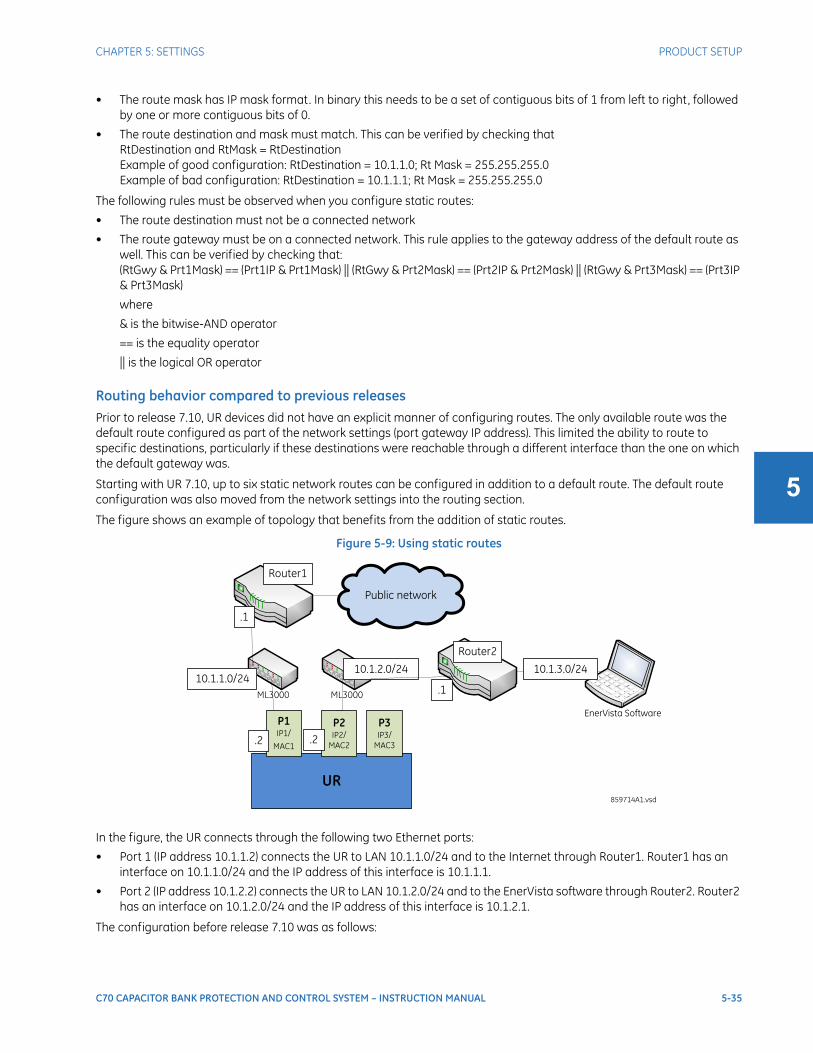
CHAPTER 5: SETTINGS PRODUCT SETUP
C70 CAPACITOR BANK PROTECTION AND CONTROL SYSTEM – INSTRUCTION MANUAL 5-35
5
• The route mask has IP mask format. In binary this needs to be a set of contiguous bits of 1 from left to right, followed by one or more contiguous bits of 0.
• The route destination and mask must match. This can be verified by checking that RtDestination and RtMask = RtDestinationExample of good configuration: RtDestination = 10.1.1.0; Rt Mask = 255.255.255.0Example of bad configuration: RtDestination = 10.1.1.1; Rt Mask = 255.255.255.0
The following rules must be observed when you configure static routes:
• The route destination must not be a connected network
• The route gateway must be on a connected network. This rule applies to the gateway address of the default route as well. This can be verified by checking that:(RtGwy & Prt1Mask) == (Prt1IP & Prt1Mask) || (RtGwy & Prt2Mask) == (Prt2IP & Prt2Mask) || (RtGwy & Prt3Mask) == (Prt3IP & Prt3Mask)
where
& is the bitwise-AND operator
== is the equality operator
|| is the logical OR operator
Routing behavior compared to previous releasesPrior to release 7.10, UR devices did not have an explicit manner of configuring routes. The only available route was the default route configured as part of the network settings (port gateway IP address). This limited the ability to route to specific destinations, particularly if these destinations were reachable through a different interface than the one on which the default gateway was.
Starting with UR 7.10, up to six static network routes can be configured in addition to a default route. The default route configuration was also moved from the network settings into the routing section.
The figure shows an example of topology that benefits from the addition of static routes.
Figure 5-9: Using static routes
In the figure, the UR connects through the following two Ethernet ports:
• Port 1 (IP address 10.1.1.2) connects the UR to LAN 10.1.1.0/24 and to the Internet through Router1. Router1 has an interface on 10.1.1.0/24 and the IP address of this interface is 10.1.1.1.
• Port 2 (IP address 10.1.2.2) connects the UR to LAN 10.1.2.0/24 and to the EnerVista software through Router2. Router2 has an interface on 10.1.2.0/24 and the IP address of this interface is 10.1.2.1.
The configuration before release 7.10 was as follows:
EnerVista Software
ML3000
Public network
UR
P1IP1/
MAC1
P2 IP2/
MAC2
ML3000
10.1.1.0/2410.1.2.0/24
P3 IP3/
MAC3
Router2
Router1
10.1.3.0/24
.1
.1
.2 .2
859714A1.vsd

5-36 C70 CAPACITOR BANK PROTECTION AND CONTROL SYSTEM – INSTRUCTION MANUAL
PRODUCT SETUP CHAPTER 5: SETTINGS
5
• PRT1 IP ADDRESS = 10.1.1.2PRT1 SUBNET IP MASK = 255.255.255.0PRT1 GWY IP ADDRESS = 10.1.1.1PRT2 IP ADDRESS = 10.1.2.2PRT2 SUBNET IP MASK = 255.255.255.0
The behavior before release 7.10 was as follows. When sending packets to EnerVista, the UR noticed that the destination was not on a connected network and it tried to find a route to destination. Since the default route was the only route it knew, it used it . Yet EnerVista was on a private network, which was not reachable through Router1. Hence a destination unreachable message was received from the router.
The configuration starting with release 7.10 is as follows:
• PRT1 IP ADDRESS = 10.1.1.2PRT1 SUBNET IP MASK = 255.255.255.0PRT2 IP ADDRESS = 10.1.2.2PRT2 SUBNET IP MASK = 255.255.255.0IPV4 DEFAULT ROUTE: GATEWAY ADDRESS = 10.1.1.1STATIC NETWORK ROUTE 1: RT1 DESTINATION = 10.1.3.0/24; RT1 NET MASK = 255.255.255.0; and RT1 GATEWAY = 10.1.2.1
The behavior since release 7.10 is as follows. There is one added static network route to the destination 10.1.3.0/24, where a computer running EnerVista is located. This static route uses a different gateway (10.1.2.1) than the default route. This gateway is the address of Router2, which has knowledge about 10.1.3.0 and is able to route packets coming from the UR and destined to EnerVista.
Show routes and ARP tablesThis feature is available on the Web interface, where the main menu contains an additional Communications menu and two submenus:
• Routing Table
• ARP Table
The tables outline the information displayed when the two submenus are selected.
Table 5-6: Routing table information
Table 5-7: IP ARP information
5.3.4.8 Modbus protocolSETTINGS PRODUCT SETUP COMMUNICATIONS MODBUS PROTOCOL
Field Description
Destination The IP address of the remote network to which this route points
Mask The network mask for the destination
Gateway The IP address of the next router to the remote network
Interface Interface through which the specified network can be reached
Field Description
IP Address The network address that corresponds to Hardware Address
Age (min) Age, in minutes, of the cache entry. A hyphen (-) means the address is local.
Hardware Address LAN hardware address, a MAC address that corresponds to network address
Type Dynamic or Static
Interface Interface to which this address mapping has been assigned
MODBUS PROTOCOL MODBUS SLAVE
ADDRESS: 254Range: 0 to 254 in steps of 1
MODBUS TCP PORTNUMBER: 502
Range: 0 to 65535 in steps of 1

CHAPTER 5: SETTINGS PRODUCT SETUP
C70 CAPACITOR BANK PROTECTION AND CONTROL SYSTEM – INSTRUCTION MANUAL 5-37
5
The serial communication ports utilize the Modbus protocol, unless the port is configured for DNP or IEC 60870-5-103 operation. This allows the EnerVista UR Setup software to be used on the port. UR devices operate as Modbus slave devices only.
For more information on the protocol, including the memory map table, see the UR Series Communications Guide.
MODBUS SLAVE ADDRESS — When using the Modbus protocol on the RS232 port, the C70 responds regardless of the MODBUS SLAVE ADDRESS programmed. For the RS485 port, each device on the serial bus must have a unique slave address from 1 to 254. Address 0 and addresses from 248 and up are reserved by the Modbus protocol specification, and so their use here is not recommended. Address 0 is the broadcast address to which all Modbus slave devices listen. When MODBUS SLAVE ADDRESS is set to 0, the C70 accepts broadcast messages, but in compliance with protocol specifications for broadcast messages, never replies. Addresses do not have to be sequential, but no two devices can have the same address or conflicts resulting in errors occur. Generally, starting at 1, set each device added to the link to use the next higher address. When using Modbus TCP/IP, the client must use the programmed MODBUS SLAVE ADDRESS value in the Unit Identifier field.
MODBUS TCP PORT NUMBER — Modbus over TCP/IP can also be used on any of the Ethernet ports. The listening TCP port 502 is reserved for Modbus communications, and only in exceptional cases when MODBUS TCP PORT NUMBER is set to any other port. The MODBUS TCP PORT NUMBER setting sets the TCP port used by Modbus on Ethernet. A MODBUS TCP PORT NUMBER of 0 disables Modbus over TCP/IP, meaning closes the Modbus TCP port. When the port number is changed to 0, the change takes effect when the C70 is restarted. When it is set to 0, use the front panel or serial port to communicate with the relay.
5.3.4.9 Protocol selectionThe PROTOCOL menu setting allows selection of one of the following protocols: DNP 3.0, IEC60870-104, or IEC60870-103. For any change to take effect, restart the unit.
The table shows which of DNP 3.0, IEC 60870-5-104, IEC 60870-5-103, and IEC 61850 protocols are operational on the RS232, RS485, and Ethernet ports. It shows all possible combinations of the PROTOCOL and DNP CHANNEL 1(2) PORT settings.
NOTE
Do not set more than one protocol to the same TCP/UDP port number, as this results in unreliable operation of those protocols.
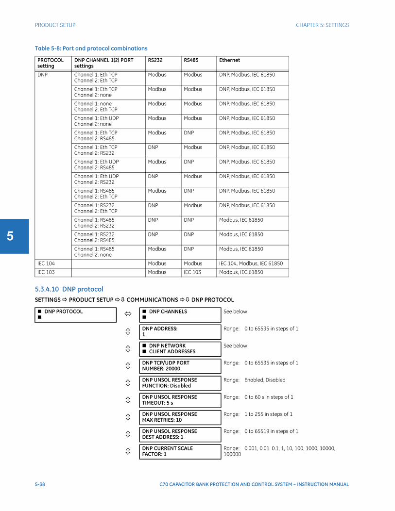
5-38 C70 CAPACITOR BANK PROTECTION AND CONTROL SYSTEM – INSTRUCTION MANUAL
PRODUCT SETUP CHAPTER 5: SETTINGS
5
Table 5-8: Port and protocol combinations
5.3.4.10 DNP protocolSETTINGS PRODUCT SETUP COMMUNICATIONS DNP PROTOCOL
PROTOCOL setting
DNP CHANNEL 1(2) PORT settings
RS232 RS485 Ethernet
DNP Channel 1: Eth TCPChannel 2: Eth TCP
Modbus Modbus DNP, Modbus, IEC 61850
Channel 1: Eth TCPChannel 2: none
Modbus Modbus DNP, Modbus, IEC 61850
Channel 1: noneChannel 2: Eth TCP
Modbus Modbus DNP, Modbus, IEC 61850
Channel 1: Eth UDPChannel 2: none
Modbus Modbus DNP, Modbus, IEC 61850
Channel 1: Eth TCPChannel 2: RS485
Modbus DNP DNP, Modbus, IEC 61850
Channel 1: Eth TCPChannel 2: RS232
DNP Modbus DNP, Modbus, IEC 61850
Channel 1: Eth UDPChannel 2: RS485
Modbus DNP DNP, Modbus, IEC 61850
Channel 1: Eth UDPChannel 2: RS232
DNP Modbus DNP, Modbus, IEC 61850
Channel 1: RS485Channel 2: Eth TCP
Modbus DNP DNP, Modbus, IEC 61850
Channel 1: RS232Channel 2: Eth TCP
DNP Modbus DNP, Modbus, IEC 61850
Channel 1: RS485Channel 2: RS232
DNP DNP Modbus, IEC 61850
Channel 1: RS232Channel 2: RS485
DNP DNP Modbus, IEC 61850
Channel 1: RS485Channel 2: none
Modbus DNP Modbus, IEC 61850
IEC 104 Modbus Modbus IEC 104, Modbus, IEC 61850
IEC 103 Modbus IEC 103 Modbus, IEC 61850
DNP PROTOCOL DNP CHANNELS
See below
DNP ADDRESS:1
Range: 0 to 65535 in steps of 1
DNP NETWORK CLIENT ADDRESSES
See below
DNP TCP/UDP PORTNUMBER: 20000
Range: 0 to 65535 in steps of 1
DNP UNSOL RESPONSEFUNCTION: Disabled
Range: Enabled, Disabled
DNP UNSOL RESPONSETIMEOUT: 5 s
Range: 0 to 60 s in steps of 1
DNP UNSOL RESPONSEMAX RETRIES: 10
Range: 1 to 255 in steps of 1
DNP UNSOL RESPONSEDEST ADDRESS: 1
Range: 0 to 65519 in steps of 1
DNP CURRENT SCALEFACTOR: 1
Range: 0.001, 0.01. 0.1, 1, 10, 100, 1000, 10000, 100000
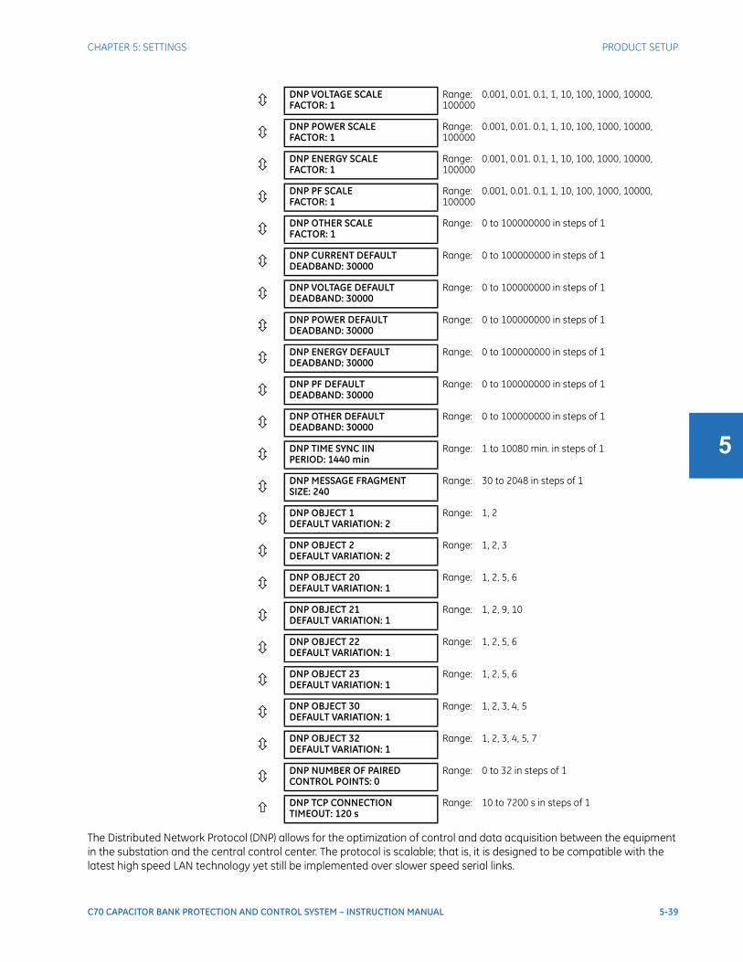
CHAPTER 5: SETTINGS PRODUCT SETUP
C70 CAPACITOR BANK PROTECTION AND CONTROL SYSTEM – INSTRUCTION MANUAL 5-39
5
The Distributed Network Protocol (DNP) allows for the optimization of control and data acquisition between the equipment in the substation and the central control center. The protocol is scalable; that is, it is designed to be compatible with the latest high speed LAN technology yet still be implemented over slower speed serial links.
DNP VOLTAGE SCALEFACTOR: 1
Range: 0.001, 0.01. 0.1, 1, 10, 100, 1000, 10000, 100000
DNP POWER SCALEFACTOR: 1
Range: 0.001, 0.01. 0.1, 1, 10, 100, 1000, 10000, 100000
DNP ENERGY SCALEFACTOR: 1
Range: 0.001, 0.01. 0.1, 1, 10, 100, 1000, 10000, 100000
DNP PF SCALEFACTOR: 1
Range: 0.001, 0.01. 0.1, 1, 10, 100, 1000, 10000, 100000
DNP OTHER SCALEFACTOR: 1
Range: 0 to 100000000 in steps of 1
DNP CURRENT DEFAULTDEADBAND: 30000
Range: 0 to 100000000 in steps of 1
DNP VOLTAGE DEFAULTDEADBAND: 30000
Range: 0 to 100000000 in steps of 1
DNP POWER DEFAULTDEADBAND: 30000
Range: 0 to 100000000 in steps of 1
DNP ENERGY DEFAULTDEADBAND: 30000
Range: 0 to 100000000 in steps of 1
DNP PF DEFAULTDEADBAND: 30000
Range: 0 to 100000000 in steps of 1
DNP OTHER DEFAULTDEADBAND: 30000
Range: 0 to 100000000 in steps of 1
DNP TIME SYNC IINPERIOD: 1440 min
Range: 1 to 10080 min. in steps of 1
DNP MESSAGE FRAGMENTSIZE: 240
Range: 30 to 2048 in steps of 1
DNP OBJECT 1DEFAULT VARIATION: 2
Range: 1, 2
DNP OBJECT 2DEFAULT VARIATION: 2
Range: 1, 2, 3
DNP OBJECT 20DEFAULT VARIATION: 1
Range: 1, 2, 5, 6
DNP OBJECT 21DEFAULT VARIATION: 1
Range: 1, 2, 9, 10
DNP OBJECT 22DEFAULT VARIATION: 1
Range: 1, 2, 5, 6
DNP OBJECT 23DEFAULT VARIATION: 1
Range: 1, 2, 5, 6
DNP OBJECT 30DEFAULT VARIATION: 1
Range: 1, 2, 3, 4, 5
DNP OBJECT 32DEFAULT VARIATION: 1
Range: 1, 2, 3, 4, 5, 7
DNP NUMBER OF PAIREDCONTROL POINTS: 0
Range: 0 to 32 in steps of 1
DNP TCP CONNECTIONTIMEOUT: 120 s
Range: 10 to 7200 s in steps of 1

5-40 C70 CAPACITOR BANK PROTECTION AND CONTROL SYSTEM – INSTRUCTION MANUAL
PRODUCT SETUP CHAPTER 5: SETTINGS
5
The DNP improves upon many master-slave protocols by improving overall communication performance requirements and provides time-stamping with millisecond accuracy.
The C70 supports the Distributed Network Protocol (DNP) version 3.0. DNP is enabled when the SETTINGS PRODUCT SETUP COMMUNICATIONS PROTOCOL setting is set to DNP 3.0. The C70 can be used as a DNP slave device connected to multiple DNP masters (usually an RTU or a SCADA master station). Since the C70 maintains two sets of DNP data change buffers and connection information, two DNP masters can actively communicate with the C70 at one time.
See the UR Series Communications Guide for more information on DNP.
The DNP Channels sub-menu is shown.
SETTINGS PRODUCT SETUP COMMUNICATIONS DNP PROTOCOL DNP CHANNELS
The DNP CHANNEL 1 PORT and DNP CHANNEL 2 PORT settings select the communications port assigned to the DNP protocol for each channel. Once DNP is assigned to a serial port, DNP is the only protocol running on that port; Modbus or IEC 60870-5-103 are disabled. If DNP is assigned to RS485, the protocol must be set to DNP on the serial port configuration as well, for the change to take effect. When the DNP CHANNEL 1(2) PORT setting is set to “Network - TCP,” the channel 1(2) DNP protocol can be used over TCP/IP on the Ethernet ports. When this value is set to “Network - UDP,” the DNP protocol can be used over UDP/IP on channel 1 only.
Changes to these port settings take effect when power has been cycled to the relay.
The DNP ADDRESS setting is the DNP slave address. This number identifies the C70 on a DNP communications link. Assign a unique address to each DNP slave.
The C70 can specify a maximum of five clients for its DNP connections. These are IP addresses for the controllers to which the C70 can connect. The settings follow.
SETTINGS PRODUCT SETUP COMMUNICATIONS DNP PROTOCOL DNP NETWORK CLIENT ADDRESSES
The DNP TCP/UDP PORT NUMBER setting is for normal DNP operation. To close the port, set the port number to 0. The change takes effect when the C70 is restarted.
The DNP UNSOL RESPONSE FUNCTION is set to “Disabled” for RS485 applications since there is no collision avoidance mechanism. The DNP UNSOL RESPONSE TIMEOUT sets the time the C70 waits for a DNP master to confirm an unsolicited response. The DNP UNSOL RESPONSE MAX RETRIES setting determines the number of times the C70 retransmits an unsolicited response without receiving confirmation from the master; a value of “255” allows infinite re-tries. The DNP UNSOL RESPONSE DEST ADDRESS is the DNP address to which all unsolicited responses are sent. The IP address to which solicited responses are sent is determined by the C70 from the current TCP connection or the most recent UDP message.
The DNP scale factor settings are numbers used to scale analog input point values. These settings group the C70 analog input data into the following types: current, voltage, power, energy, power factor, and other. Each setting represents the scale factor for all analog input points of that type. For example, if the DNP VOLTAGE SCALE FACTOR setting is set to “1000,” all DNP analog input points that are voltages are returned with values 1000 times smaller (for example, a value of 72000 V on the C70 is returned as 72). These settings are useful when analog input values must be adjusted to fit within certain
DNP CHANNELS DNP CHANNEL 1 PORT:
NONERange: NONE, COM2 - RS485, FRONT PANEL - RS232, NETWORK - TCP, NETWORK - UDP
DNP CHANNEL 2 PORT:NONE
Range: NONE, COM2 - RS485, FRONT PANEL - RS232, NETWORK - TCP
NOTE
Do not set more than one protocol to the same TCP/UDP port number, as this results in unreliable operation of those protocols.
DNP NETWORK CLIENT ADDRESSES CLIENT ADDRESS 1:
0.0.0.0Range: standard IP address
CLIENT ADDRESS 5:0.0.0.0
Range: standard IP address
CHAPTER 5: SETTINGS PRODUCT SETUP
C70 CAPACITOR BANK PROTECTION AND CONTROL SYSTEM – INSTRUCTION MANUAL 5-41
5
ranges in DNP masters. Note that a scale factor of 0.1 is equivalent to a multiplier of 10 (that is, the value is 10 times larger).
The DNP DEFAULT DEADBAND settings determine when to trigger unsolicited responses containing analog input data. These settings group the C70 analog input data into the following types: current, voltage, power, energy, power factor, and other. Each setting represents the default deadband value for all analog input points of that type. For example, to trigger unsolicited responses from the C70 when any current values change by 15 A, the DNP CURRENT DEFAULT DEADBAND setting is set to “15.” Note that these settings are the deadband default values. DNP object 34 points can be used to change deadband values, from the default, for each individual DNP analog input point. Whenever power is removed and re-applied to the C70, the default deadbands are in effect.
The DNP TIME SYNC IIN PERIOD setting determines how often the Need Time Internal Indication (IIN) bit is set by the C70. Changing this time allows the DNP master to send time synchronization commands more or less often, as required.
The DNP MESSAGE FRAGMENT SIZE setting determines the size, in bytes, at which message fragmentation occurs. Large fragment sizes allow for more efficient throughput; smaller fragment sizes cause more application layer confirmations to be necessary, which provides more robust data transfer over noisy communication channels.
The DNP OBJECT 1 DEFAULT VARIATION to DNP OBJECT 32 DEFAULT VARIATION settings select the DNP default variation number for object types 1, 2, 20, 21, 22, 23, 30, and 32. The default variation refers to the variation response when variation 0 is requested and/or in class 0, 1, 2, or 3 scans. See the DNP Implementation section in the UR Series Communications Guide.
The DNP binary outputs typically map one-to-one to IED data points. That is, each DNP binary output controls a single physical or virtual control point in an IED. In the C70 relay, DNP binary outputs are mapped to virtual inputs. However, some legacy DNP implementations use a mapping of one DNP binary output to two physical or virtual control points to support the concept of trip/close (for circuit breakers) or raise/lower (for tap changers) using a single control point. That is, the DNP master can operate a single point for both trip and close, or raise and lower, operations. The C70 can be configured to support paired control points, with each paired control point operating two virtual inputs. The DNP NUMBER OF PAIRED CONTROL POINTS setting allows configuration of 0 to 32 binary output paired controls. Points not configured as paired operate on a one-to-one basis.
The DNP TCP CONNECTION TIMEOUT setting specifies a time delay for the detection of dead network TCP connections. If there is no data traffic on a DNP TCP connection for greater than the time specified by this setting, the connection is aborted by the C70. This frees up the connection to be re-used by a client. Any change takes effect after cycling power to the relay.
5.3.4.11 DNP / IEC 60870-5-104 point listsSETTINGS PRODUCT SETUP COMMUNICATIONS DNP / IEC104 POINT LISTS
Up to 256 binary and up to 256 analog input points for the DNP protocol, or the MSP and MME points for IEC 60870-5-104 protocol, can be configured. The value for each point is user-programmable and can be configured by assigning FlexLogic operands for binary inputs / MSP points or FlexAnalog parameters for analog inputs / MME points.
The menu for the binary input points (DNP) or MSP points (IEC 60870-5-104) follows.
NOTE
The C70 relay does not support energy metering. As such, the DNP ENERGY SCALE FACTOR and DNP ENERGY DEFAULT DEADBAND settings are not applicable.
NOTE
Check the “DNP Points Lists” C70 web page to view the analog inputs and/or binary inputs points lists. This page can be viewed with a web browser by entering the IP address of the C70 Ethernet port employed to access the C70 Main Menu, then by clicking the Device Information Menu item, then the DNP Points Lists item.
DNP / IEC104 POINT LISTS BINARY INPUT / MSP
POINTSSee below
ANALOG INPUT / MME POINTS
See below

5-42 C70 CAPACITOR BANK PROTECTION AND CONTROL SYSTEM – INSTRUCTION MANUAL
PRODUCT SETUP CHAPTER 5: SETTINGS
5
SETTINGS PRODUCT SETUP COMMUNICATIONS DNP / IEC104 POINT LISTS BINARY INPUT / MSP POINTS
Up to 256 binary input points can be configured for the DNP or IEC 60870-5-104 protocols. The points are configured by assigning an appropriate FlexLogic operand. See the Introduction to FlexLogic section in this chapter for the range of assignable operands.
Changes to the DNP / IEC 60870-5-104 point lists take effect when the C70 is restarted.
The menu for the analog input points (DNP) or MME points (IEC 60870-5-104) follows.
SETTINGS PRODUCT SETUP COMMUNICATIONS DNP / IEC104 POINT LISTS ANALOG INPUT / MME POINTS
Up to 256 analog input points can be configured for the DNP or IEC 60870-5-104 protocols. The analog point list is configured by assigning an appropriate FlexAnalog parameter to each point. See the FlexAnalog Parameters section in Appendix A for the range of assignable parameters.
Changes to the DNP / IEC 60870-5-104 point lists take effect when the C70 is restarted.
5.3.4.12 IEC 61850 protocol
The IEC 61850 settings are accessible in EnerVista software or a substation configuration language (SCL) generating tool. The path is Settings > Product Setup > Communications > IEC 61850. The settings are not accessible from the front panel of the device.
BINARY INPUT / MSP POINTS Point: 0
OffRange: FlexLogic operand
Point: 1Off
Range: FlexLogic operand
Point: 255Off
Range: FlexLogic operand
ANALOG INPUT / MME POINTS Point: 0
OffRange: any FlexAnalog parameter
Point: 1Off
Range: any FlexAnalog parameter
Point: 255Off
Range: any FlexAnalog parameter
NOTE
The DNP / IEC 60870-5-104 point lists always begin with point 0 and end at the first “Off” value. Since DNP / IEC 60870-5-104 point lists must be in one continuous block, any points assigned after the first “Off” point are ignored.
The C70 is provided with optional IEC 61850 communications capability. This feature is specified as a software option at the time of ordering. See the Order Codes section in chapter 2 for details.
NOTE
IEC 61850 messaging can form part of protection schemes. Consider IEC 61850 settings with the same criticality as protection element settings. To ensure reliable performance of protection schemes utilizing IEC 61850 messaging, route IEC 61850 traffic on a separate port from SCADA communications, or use redundant, independent ports, and a high speed network recovery method, such as PRP.

CHAPTER 5: SETTINGS PRODUCT SETUP
C70 CAPACITOR BANK PROTECTION AND CONTROL SYSTEM – INSTRUCTION MANUAL 5-43
5
OverviewIEC 61850 is a series of international standards and technical reports applicable to power utility automation systems. It includes semantics, abstract communication services, specific communication services, performance specifications, network engineering guidelines, configuration description methodologies, and engineering processes. The standard enables interoperability among intelligent electronic devices (IEDs) from different suppliers and interoperability among software configuration tools from different suppliers. Interoperability in this case is the ability for IEDs to operate on the same network or communication path sharing information and commands, and for configuration tools to understand each other's configuration files.
The UR series supports a large subset of IEC 61850 features. These are detailed in the UR Series Communications Guide and include the information model, GOOSE publish, GOOSE subscribe, buffered report server, unbuffered report server, and Manufacturing Message Specification (MMS) query, read, write, and control services. In addition, the UR and EnerVista UR Setup software support IEC 61850 Substation Configuration Language (SCL) file import/export.
Whereas prior UR releases used edition 1.0 of IEC 61850, this release uses edition 2.0, with certain modifications according to IEC/TR 61850-90-5. Only edition 2.0 61850 configuration tools can interoperate with edition 2.0 devices such as the UR 7.3x release. The UR release uses edition 2.0 SCL, which differs from edition 1.0 SCL. GSSE, fixed GOOSE, and fixed report services of previous releases are no longer supported, and thus UR devices of previous releases using these features have to be converted to configurable GOOSE to communicate with a 7.3x device.
Many settings of UR protection, control, and monitoring elements, that is to say elements that are not concerned with the IEC 61850 protocol, can nevertheless be accessed via IEC 61850. These settings are documented elsewhere in this Settings chapter. This section of the Settings chapter deals solely with the settings that configure the IEC 61850 protocol itself.
The maximum number of simultaneous clients supported by the UR series is five.
EnerVista setup for IEC 61850The EnerVista UR Setup software provides the interface to configure C70 settings for the IEC 61850 protocol. This section describes this interface. The software also supports import and export of IEC 61850 Substation Configuration Language (SCL) files as documented in the UR Series Communications Guide.
Unlike other UR settings, IEC 61850 protocol configuration settings cannot be accessed through the UR front panel. These settings are accessible with the EnerVista software, via MMS query, read, and write services, or via 61850 Substation Configuration Language (SCL) file transfer. Accordingly, whereas other settings are presented in this manual as they appear on the front panel, IEC 61850 settings are presented as they appear in the software. See the UR Series Communications Guide for MMS and SCL access. Note that if you update the IEC 61850 settings in the EnerVista software by writing to them by MMS while the corresponding IEC 61850 panel is open in EnerVista, you need to close then open the panel in EnerVista for the correct readings to display.
All IEC 61850 protocol configuration settings are accessed through software panels that are selected either in the Online Window area (see figure) or the Offline Window area in the EnerVista software.
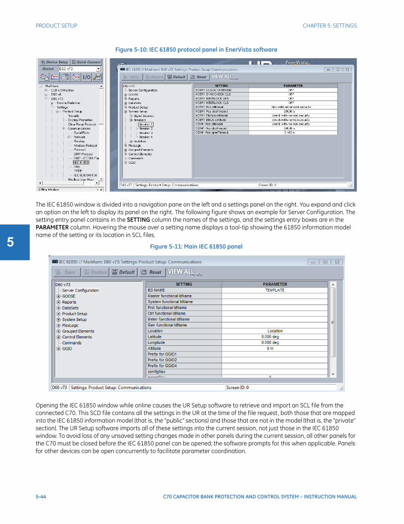
5-44 C70 CAPACITOR BANK PROTECTION AND CONTROL SYSTEM – INSTRUCTION MANUAL
PRODUCT SETUP CHAPTER 5: SETTINGS
5
Figure 5-10: IEC 61850 protocol panel in EnerVista software
The IEC 61850 window is divided into a navigation pane on the left and a settings panel on the right. You expand and click an option on the left to display its panel on the right. The following figure shows an example for Server Configuration. The setting entry panel contains in the SETTING column the names of the settings, and the settings entry boxes are in the PARAMETER column. Hovering the mouse over a setting name displays a tool-tip showing the 61850 information model name of the setting or its location in SCL files.
Figure 5-11: Main IEC 61850 panel
Opening the IEC 61850 window while online causes the UR Setup software to retrieve and import an SCL file from the connected C70. This SCD file contains all the settings in the UR at the time of the file request, both those that are mapped into the IEC 61850 information model (that is, the "public" sections) and those that are not in the model (that is, the "private" section). The UR Setup software imports all of these settings into the current session, not just those in the IEC 61850 window. To avoid loss of any unsaved setting changes made in other panels during the current session, all other panels for the C70 must be closed before the IEC 61850 panel can be opened; the software prompts for this when applicable. Panels for other devices can be open concurrently to facilitate parameter coordination.

CHAPTER 5: SETTINGS PRODUCT SETUP
C70 CAPACITOR BANK PROTECTION AND CONTROL SYSTEM – INSTRUCTION MANUAL 5-45
5
The Restore button restores all settings in the IEC 61850 window to their last saved values. The Default button causes all settings in the IEC 61850 window to revert to factory default values. Both buttons affect the current panel being displayed. Neither button affects settings in other than the IEC 61860 window.
Create CID and settings filesWhen the Save button in the online IEC 61850 window is clicked, UR Setup software prepares a configured IED description (CID) file containing all the device’s settings and sends the CID file to the connected C70. On receipt of a CID file, the C70 checks it for correctness, and if no error is found, reboots using the settings in the CID file. UR Setup displays a message when the C70 is running the new settings, confirming successful transfer. This process can take a minute or so due to the extensive amount of processing required by the software and the C70.
Certain settings not related to IEC 61850 are indicated in this manual as taking effect only when the device is restarted. The reboot following CID file transfer described in the previous paragraph does not make these setting changes take effect, as the C70 does not accept the setting change until after the CID file transfer reboot. For any change in the indicated settings to take effect, after the automatic restart due to CID file transfer, you must perform a manual restart, for example by executing the Maintenance > Reboot Relay Command in the software.
When the Save button in the offline IEC 61850 window is clicked, UR Setup software saves to local storage, for example the hard drive, a .urs file containing all of the device's settings.
Server configurationThe Server Configuration panel contains IEC 61850 settings relevant to the server functions of the IED implementation.
The path is Settings > Product Setup > Communications > IEC 61850 > Server Configuration.
The following settings are available, where <iedName> is a syntactic variable representing the present value of the IED NAME setting.
IED NAMERange: 1 to 64 VisibleString charactersDefault: TEMPLATE
The value entered sets the IED name used by IEC 61850 for the C70. An IED name unique within the network must be entered for proper operation. Valid characters are upper and lowercase letters, digits, and the underscore (_) character. The first character must be a letter.
Master functional ldNameRange: 0 to 64 VisibileString charactersDefault:
The Master logical device contains the UR logical nodes modelling communications and setting group control. Valid characters are upper and lowercase letters, digits, and the underscore (_) character. If the number of characters entered is greater than zero, this setting sets the name used in communications for the Master logical device. If an ldName is entered, a name unique within the network must be entered for proper operation. The standard recommends choosing this name according to IEC 81346-1. If the number of characters entered is zero, the name used in communications for the Master logical device is "<iedName>Master", where <iedName> is the value of setting IED NAME described earlier.
NOTE
Throughout the remainder of this section, <LDName> is a syntactic variable representing the present name of the master logical device. Depending on its context, <LDName> can be a product-related name or a function-related name. In SCL files, <LDName> is always the product-related name. In IEC 61850 messages, <LDName> is the function-related name if one is set by the Master functional ldName setting, otherwise <LDName> is again the product-related name. The product-related name of the Master logical device is "<iedName>Master". The function related name of the Master logical device is the value of the Master functional ldName setting.

5-46 C70 CAPACITOR BANK PROTECTION AND CONTROL SYSTEM – INSTRUCTION MANUAL
PRODUCT SETUP CHAPTER 5: SETTINGS
5
System functional ldNameRange: 0 to 64 VisibileString charactersDefault:
This setting is similar to setting Master functional ldName, but is for the System logical device, which contains the UR logical nodes modelling power system devices: breakers, switches, CTs, VTs, and so on, including interface to these such as AC inputs, contact I/O, transducer I/O, and HardFiber I/O.
Prot functional ldNameRange: 0 to 64 VisibileString charactersDefault:
This setting is similar to setting Master functional ldName, but is for the Prot logical device instance, which contains the UR logical nodes modelling protection and protection related functions.
Ctrl functional ldNameRange: 0 to 64 VisibileString charactersDefault:
This setting is similar to setting Master functional ldName, but is for the Ctrl logical device instance, which contains the UR logical nodes modelling control and monitoring functions.
Meter functional ldNameRange: 0 to 64 VisibileString charactersDefault:
This setting is similar to setting Master functional ldName, but is for Meter the logical device instance, which contains the UR logical nodes modelling metering and measurement (other than PMU), including Signal Sources.
Gen functional ldNameRange: 0 to 64 VisibileString charactersDefault:
This setting is similar to setting Master functional ldName, but is for the Gen logical device instance, which contains the UR logical nodes modelling FlexLogic, Virtual Outputs, non-volatile latches, FlexElements, recording (for example oscillography), security, front panel, and clock.
LocationRange: 0 to 255 ASCII charactersDefault: Location
The value entered sets the value of the data attribute <LDName>/LPHD1.PhyNam.location. This data attribute is provided by the protocol to allow the user to declare where the equipment is installed.
LatitudeRange: -90.000 to 90.000 degrees in steps of 0.001 degreeDefault: 0.000 deg
The value entered sets the value of the data attribute <LDName>/LPHD1.PhyNam.latitude. This data attribute is provided by the protocol to allow the user to declare the geographical position of the device in WGS84 coordinates -latitude. Negative values indicate a southern latitude. WGS refers to the world geodetic system, which is used in global positioning systems (GPS), and 84 is the current version of the standard.
LongitudeRange: -180.000 to 180.000 degrees in steps of 0.001 degreeDefault: 0.000 deg
The value entered sets the value of the data attribute <LDName>/LPHD1.PhyNam.longitude. This data attribute is provided by the protocol to allow the user to declare the geographical position of the device in WGS84 coordinates -longitude. Negative values indicate a western longitude.

CHAPTER 5: SETTINGS PRODUCT SETUP
C70 CAPACITOR BANK PROTECTION AND CONTROL SYSTEM – INSTRUCTION MANUAL 5-47
5
AltitudeRange: 0 to 10,0000 m in steps of 1 mDefault: 0 m
The value entered sets the value of the data attribute <LDName>/LPHD1.PhyNam.altitude. This data attribute is provided by the protocol to allow the user to declare the geographical position of the device in WGS84 coordinates - altitude.
Prefix for GGIO1Range: 0 to 7 VisibleString charactersDefault:
This setting sets the LN Prefix of the logical node GGIO1 that is described in the GGIO1 section later. Valid characters are upper and lowercase letters, digits, and the underscore (_) character. The first character must be a letter.
Prefix for GGIO2Range: 0 to 7 VisibleString charactersDefault:
This setting sets the LN Prefix of logical node GGIO2 that is described in the GGIO2 section later. Valid characters are upper and lowercase letters, digits, and the underscore (_) character. The first character must be a letter.
Prefix for GGIO4Range: 0 to 7 VisibleString charactersDefault:
This setting sets the LN Prefix of logical node GGIO4 that is described in the GGIO4 section later. Valid characters are upper and lowercase letters, digits, and the underscore (_) character. The first character must be a letter.
Master configRevRange: 0 to 255 ASCII charactersDefault:
This data attribute is provided by the protocol to allow the user to declare changes to the semantic of the data model of the UR. The intent is that the user changes Master configRev each time that the semantic or data model changes, so that clients can readily detect the change. A semantic change is a logical node getting a new semantic use; for example, an instance of logical node CSWI is now serving a different physical switch, or an instance of a logical node PDIS is now used for another zone. A data model change is a change in the presence of logical nodes, data objects, data attributes, or instance names.
The scope of Maser configRev is the entire relay configuration as the Master logical device is the root logical device. Similar settings are provided for the other logical nodes; the scope of these other configRev settings is limited to the corresponding logical device configuration.
paramRevRange: -2,147,483,648 to 2,147,483,647 in steps of 1Default: 0
This data attribute is provided by the protocol to make changes to the settings of the C70 apparent to clients. The Substation Configuration Tool and UR Setup software advance the value of paramRev each time any setting changes. The C70 increments the value of parmRev when a setting change is made other than through CID file download.
LLN0.Mod.ctlModelRange: status-only, direct-with-normal-security, sbo-with-normal-securityDefault: sbo-with-normal-security
This setting specifies the control service that clients must use to control the TEST MODE FUNCTION of the C70. An "on" control to <LDName>/LLN0.Mod changes TEST MODE FUNCTION to Disabled, an "on-blocked" control changes it to Forcible, and a "test/blocked" changes it to Isolated.
IEC/MMS TCP PORT NUMBERRange: 0 to 65535 in steps of 1Default: 102
This setting allows the user to change the TCP port number for Manufacturing Message Specification (MMS) connections. It is recommended that this setting be left at the default value.

5-48 C70 CAPACITOR BANK PROTECTION AND CONTROL SYSTEM – INSTRUCTION MANUAL
PRODUCT SETUP CHAPTER 5: SETTINGS
5
Configuration TypeRange: G2, E3-2.0Default: G2
This setting specifies the method used to describe GOOSE subscription configuration in SCL. See the UR Series Communications Guide for details. Basically, in the G2 mode, the CID file contains IED elements for IEDs subscribed to by this IED containing GOOSE subscription information. In the E3 2.0 mode, the CID file has only one IED element and GOOSE subscription information is coded in data objects in the standard LGOS logical node used to monitor reception of the subscribed GOOSE. UR 7.30 or later accepts either mode.
GOOSEThe path is Settings > Product Setup > Communications > IEC 61850 > GOOSE.
Figure 5-12: IEC 61850 TxGOOSE Access Points panel
TxGOOSE
IEC 61850 GOOSE is an efficient method for simultaneous high-speed delivery of a set of generic substation event information in a publishing physical device to more than one subscribing physical device. A TxGOOSE is a UR element implementing a single IEC 61850 GOOSE message publishing service. The subscribing function in URs is performed by RxGOOSE elements, as described in the next section. Each UR with IEC 61850 order code options has eight TxGOOSE elements. Each TxGOOSE element can publish the values of up to 64 FlexLogic or FlexAnalog operands in the UR.
Published TxGOOSE messages configured in the EnerVista UR Setup software can be subscribed by and the published operand values understood by other UR devices. In fact, they can be subscribed to and understood by any device of any manufacturer that implements the IEC 61850 edition 1.0 or 2.0 GOOSE subscription mechanism. The messages are published with a multicast address so that the network sends the messages to all devices; any number of devices that want to subscribe can.
The entities whose values are published in GOOSE messages are known as members. The members are itemized in an ordered list known as a data set. Each TxGOOSE can use any one of the data sets provided. See the DataSets section later for details.
NOTE
Do not set more than one protocol to the same TCP/UDP port number, as this results in unreliable operation of those protocols.

CHAPTER 5: SETTINGS PRODUCT SETUP
C70 CAPACITOR BANK PROTECTION AND CONTROL SYSTEM – INSTRUCTION MANUAL 5-49
5
Each enabled TxGOOSE transmits its message whenever a value change is detected in one or more of its members. To guard against the possibility that such a message is lost in the network before it reaches all subscribers, the message is quickly retransmitted several times. To allow subscribers to verify that their link to the publisher and the publisher itself are healthy, each message is also periodically retransmitted even while the values are unchanging. These latter messages are known as heartbeat messages, while the former are known as event messages. Heartbeat messages also provide means for a subscriber newly online to receive the published values in the absence of an event.
TxGOOSE1 and TxGOOSE2 scan for value changes in its FlexLogic operand members as frequently as such a change can occur. TxGOOSE1 and TxGOOSE2 are therefore suitable for highly time critical signals, such as tripping and dynamic blocking. FlexAnalog members are scanned for value changes only every 250 ms. See the Deadband Settings section later for a description of what is considered a value change in an analog member.
The remaining TxGOOSE, meaning TxGOOSE3 and up, scan both their FlexLogic and FlexAnalog members for value changes every 250 ms. They are suited for control applications, such as voltage control or power factor regulation.
The details of TxGOOSE message construction are contained in the UR Series Communications Guide. Knowledge of these details is not required to configure GOOSE.
The UR does not implement the Fixed-Length encoded GOOSE messages option specified in IEC 61850-8-1:2011 clause A.3; the UR always uses the ASN.1 Basic encoding rules (as specified in ISO/IEC 8825-1) as specified in IEC 61850-8-1:2004 and as optional in IEC 61850-8-1:2011 clause A.3. So do not try to configure the UR for fixed-offset TxGOOSE.
TxGOOSE
Navigate to Settings > Product Setup > Communications > IEC 61850 > GOOSE > TxGOOSE > Access Points to access the settings that are common to all GOOSE messages published.
The following settings are available.
PORT1 GOOSE ENABLERange: Enabled, DisabledDefault: Enabled
When set to Disabled, no GOOSE messages are published on C70 Ethernet port 1, and any GOOSE messages received on port 1 are ignored. When set to Enabled, all enabled GOOSE messages are published on C70 Ethernet port 1, and any GOOSE messages received on port 1 are listened to.
C70 Ethernet ports 2 and 3 each have a similar setting.
TxGOOSE UPDATE TIMERange: 1 to 60 s in steps of 1 sDefault: 60 s
This setting specifies the time interval between heartbeat messages, which are messages that are sent periodically while no events are detected. The standard suggests that the heartbeat time be less than (actually half) of the timeAllowedtoLive parameter, which is set by the TxGOOSE TIME TO LIVE settings described later.
Navigate to Settings > Product Setup > Communications > IEC 61850 > GOOSE > TxGOOSE > TxGOOSE1 to access the settings for the first TxGOOSE. The settings and functionality for the others are similar.

5-50 C70 CAPACITOR BANK PROTECTION AND CONTROL SYSTEM – INSTRUCTION MANUAL
PRODUCT SETUP CHAPTER 5: SETTINGS
5
Figure 5-13: IEC 61850 TxGOOSE panel
TxGOOSE1 FUNCTIONRange: Enabled, DisabledDefault: Enabled
When set to Disabled, TxGOOSE1 messages are not published. When set to Enabled, TxGOOSE1 messages are published.
When TxGOOSE1 to 8 are set to Disabled in EnerVista and subsequently Enabled by writing via MMS, the panel continues to read Disabled until relaunched. There is no polling capability to update automatically the IEC 61860 readings, so the panel needs to be closed then opened for the correct status to display.
TxGOOSE1 GoIDRange: 0 to 129 VisibleString charactersDefault: TxGOOSE1
The entered value sets the goID value published in TxGOOSE1 messages, and can be used by subscribers to discriminate the TxGOOSE1 messages from other GOOSE messages.
TxGOOSE1 DatSetRange: None, DataSet01, DataSet02,...Default: None
This setting selects the published data set using the UR Setup software designator for the data set. The IEC 61850 name of the data sets are configured in the Datasets panel, as described later.
An ObjectReference to the data set, which consists of the concatenation of the string "<LDName>/LLN0." and the data set name, is published in the datSet field of TxGOOSE1 messages and can be used by subscribers to discriminate TxGOOSE1 messages from other GOOSE messages.
TxGOOSE1 DST MACRange: any 12 digit hexadecimal numberDefault: 01-0C-CD-01-00-00
The value entered sets the Ethernet destination Media Access Control (MAC) address in published TxGOOSE1 messages. As the standard requires that the address have the multicast bit set TRUE, that is to say the second digit is set to an odd number, messages transmitted have the multicast bit set TRUE no matter its value in this setting.
The destination MAC address can be used by the network to restrict message delivery to selected devices that need to receive them, reducing network loading. This address also can be used by hardware in receiving devices to filter out messages that are of no interest to them, reducing processor burden. Different filtering algorithms are implemented by different devices. The standard recommends that the algorithm used by hardware of the receiving device be considered when assigning destination multicast addresses.
Subscribers can use this address to discriminate TxGOOSE1 messages from other GOOSE messages.
CHAPTER 5: SETTINGS PRODUCT SETUP
C70 CAPACITOR BANK PROTECTION AND CONTROL SYSTEM – INSTRUCTION MANUAL 5-51
5
TxGOOSE1 VLAN PRIORITYRange: 0, 1, 2, 3, 4, 5, 6, 7, 5-4, 6-4, 6-5, 7-4, 7-5, 7-6Default: 4
When the value entered is 0, 1, 2, 3, 4, 5, 6, or 7, the User Priority value in the IEEE 802.1Q VLAN tag included in published TxGOOSE1 messages is set to that value. When one of the two-digit values is entered, the dynamic priority feature is selected: the first event message has the User Priority value of the first digit, and User Priority is decremented in each following message until reaching the value of the second digit. For instance, if the selected value is 7-5, then the User Priority values in successive messages beginning with the message triggered by an event is 7, 6, 5, 5, 5, 5, 5, and so on. Do not make a dynamic priority selection when standard behavior is required.
Network devices can forward a message with a higher priority value before a message with a lower priority value, which speeds delivery of high priority messages in heavily loaded networks. The standard recommends that higher priority messages, such as GOOSE, have priority values in the range of 4 to 7.
TxGOOSE1 VLAN IDRange: 0 to 4095 in steps of 1Default: 0
The value entered sets the VID value in the IEEE 802.1Q VLAN tag included in published TxGOOSE1 messages. VID can be used by network devices to direct messages to only selected devices, reducing network burden. VID values of 0 and 1 are assigned by IEEE 802.1Q to other functions and are not to be used for GOOSE.
TxGOOSE1 ETYPE APPIDRange: 0 to 65535 in steps of 1Default: 0
The value entered sets the APPID value in published GOOSE messages and can be used by subscribers to discriminate TxGOOSE1 messages from other GOOSE messages.
The standard reserves the value range 0 to 16383 for GOOSE Type 1 (Fast messages), and reserves the value range 32768 to 41151 for GOOSE Type 1A (Trip messages). Some subscribers can process messages in the Type 1A range faster than messages in the Type 1 range. The standard reserves the default value (0) to indicate lack of configuration. The standard strongly recommends unique, source-orientated APPIDs within a given system.
TxGOOSE1 ConfRevRange: 0 to 4294967295 in steps of 1Default: 1
The value entered sets the confRev value in published GOOSE messages, and can be used by subscribers to discriminate TxGOOSE messages of the expected configuration revision from messages of a different revision. The standard requires that confRef be incremented each time the members or the order of the members published is changed, and each time the data set name is changed. The standard states that the value of 0 is reserved.
TxGOOSE1 RETRANS TIMERange: 0 to 100 ms in steps of 1 msDefault: 4 ms
If the entered time is non-zero, when a member value change is detected, four event transmissions are sent, then heartbeat transmissions resume. The interval between the first and second event transmissions, and between the second and third, is the time set here. The interval between the third and the fourth event transmission is double the set time. If the entered time is zero, only a single event transmission occurs, then heartbeat transmissions resume.
TxGOOSE1 TIME TO LIVERange: 1 to 300 s in steps of 1 sDefault: 300 s
The value entered sets the timeAllowedtoLive value in published TxGOOSE1 messages. The standard requires subscribers to assume a failure has occurred when another TxGOOSE1 message is not received within the published timeAllowedtoLive time.

5-52 C70 CAPACITOR BANK PROTECTION AND CONTROL SYSTEM – INSTRUCTION MANUAL
PRODUCT SETUP CHAPTER 5: SETTINGS
5
Base this setting on the TxGOOSE UPDATE TIME and the tolerable number of contiguous message delivery misses. For example, if the heartbeat time is 10 s, and missing up to three successive messages is tolerable, make the setting 10*3 + 1 = 31 s. The extra second is to ensure that arrival of the third heartbeat transmission beats the timeAllowedtoLive timer. The standard suggests that the heartbeat time be less than (actually half) of the timeAllowedtoLive parameter.
RxGOOSE
Navigate to Settings > Product Setup > Communications > IEC 61850 > GOOSE > RxGOOSE > RxGOOSE Messages.
IEC 61850, GOOSE is an efficient method for simultaneous high-speed delivery of the same generic substation event information in a publishing physical device to more than one subscribing physical device. An RxGOOSE is a UR element implementing a single IEC 61850 GOOSE message subscribing service. The publishing function in URs is performed by TxGOOSE elements, as described in the previous section. Each C70 has 16 RxGOOSE elements. Each RxGOOSE element can subscribe to GOOSE messages from a specified publisher. Subscribed messages can contain up to 64 of any set of data attributes with basic types BOOLEAN, FLOAT32, INT32, Dbpos, TimeStamp, or Quality. Messages containing data objects, that is to say structured data, are not accepted.
With these conditions, GOOSE messages from any device of any manufacturer that implements the IEC 61850 edition 1.0 or 2.0 GOOSE publish service can be subscribed to. The UR accepts both the variable-length encoded GOOSE messages specified in IEC 61850-8-1:2004 and the Fixed-Length encoded GOOSE messages as specified in IEC 61850-8-1:2011 clause A.3.
Each enabled RxGOOSE monitors for interruption of the GOOSE messages that it subscribes to based on the value in the timeAllowedtoLive field of the last message received. If a new message is not received within that time interval, the RxGOOSE assumes that connectivity is lost. FlexLogic operands (for example, RxGOOSE1 On, RxGOOSE1 Off) reflect the status of each RxGOOSE connectivity. RxGOOSE connectivity of an RxGOOSE with non-zero MAC address is also considered lost after the C70 finishes restart until a message is received. When RxGOOSE connectivity is lost, a common RxGOOSE Fail self-test activates.
Navigate to Settings > Product Setup > Communications > IEC 61850 > GOOSE > RxGOOSE > RxGOOSE Messages > RxGOOSE1 to access the settings that specify the messages to be accepted by the first RxGOOSE element. Messages that contain the value true in the ndsCom field are never accepted. Messages that contain the value true in the simulation field (test field in edition 1.0 messages) are accepted only when the UR test mode is Forcible; see the Testing section at the end of this chapter for details. The settings and functionality for the other RxGOOSE are similar.
Navigate to Settings > Product Setup > Communications > IEC 61850 > GOOSE > RxGOOSE > RxGOOSE Messages > RxGOOSE1. The following settings are available.
Figure 5-14: IEC 61850 RxGOOSE Messages panel

CHAPTER 5: SETTINGS PRODUCT SETUP
C70 CAPACITOR BANK PROTECTION AND CONTROL SYSTEM – INSTRUCTION MANUAL 5-53
5
RxGOOSE1 IDRange: 0 to 129 VisibleString charactersDefault:
If the value entered has one or more characters, the goID field of incoming GOOSE messages must exactly match this value for the message to be accepted as a valid RxGOOSE1 message. If the entered value is the empty string, RxGOOSE1 does not check the value received in the goID field.
RxGOOSE1 Dst MACRange: any 12 digit hexadecimal numberDefault: 00-00-00-00-00-00
Set this setting to the MAC address of the publisher. Only received GOOSE messages having a Media Access Control (MAC) address equal to this value are accepted as valid RxGOOSE1 messages. An entered address of zero disables RxGOOSE1.
If the publisher is a UR Series 7.3x device, the setting needs to match the value of the publisher’s TxGOOSE Dst MAC setting.
RxGOOSE1 ETYPE APPIDRange: 0 to 65535 in steps of 1Default: 0
If the value entered is non-zero, the APPID field of incoming GOOSE messages must exactly match this value for the message to be accepted as a valid RxGOOSE1 message. If the value entered is zero, RxGOOSE1 does not check the value received in the APPID field.
If the publisher is a UR Series 7.3x device, the setting needs to match the value of the publisher’s TxGOOSE ETYPE APPID setting.
RxGOOSE1 GoCBRefRange: 0 to 129 alphanumeric, underscore, slash and period characters, beginning with an alpha characterDefault:
The gocbRef field of incoming GOOSE messages must match this value for the message to be accepted as a valid RxGOOSE1 message. If the entered value is the empty string, RxGOOSE1 is disabled. If not the empty string, the entry needs to be an ACSI ObjectReference to the publishing control block in the format:
<LDName>/LLN0.<GoCBName>
where <LDName> is the function-related name if any of the logical device containing the publishing control block, otherwise the product-related name of that logical device, and <GoCBName> is the name of the publishing control block.
The C70 translates the ACSI format required for this setting to the MMS format used in GOOSE messages:
<LDName>/LLN0$GO$<GoCBName>
If the publisher is a UR 7.3x series device, <LDName> is the value of the publisher's Master functional ldName setting if that setting is not empty, otherwise it is the value of the publisher's IED NAME suffixed with "Master". If the publisher is a UR 7.3x series device, <GoCBName> is "GoCB" suffixed with the two digit TxGOOSE instance number, for example "GoCB01".
RxGOOSE1 datSetRange: 0 to 32 alphanumeric and underscore characters, beginning with an alpha characterDefault:
If the entered value has one or more characters, the datSet field of incoming GOOSE messages must exactly match this value prefixed by <LDName>/LLN0$ for the message to be accepted as a valid RxGOOSE1 message. <LDName> is as specified in the RxGOOSE GoCBRef setting above. If the entered value is the empty string, RxGOOSE1 does not check the value received in the datSet field.
If the publisher is a UR 7.3x series device, set this setting to the value of the publisher's DataSetxx name setting, where xx is the instance number of the data set selected by the publisher's TxGOOSE datSet setting.

5-54 C70 CAPACITOR BANK PROTECTION AND CONTROL SYSTEM – INSTRUCTION MANUAL
PRODUCT SETUP CHAPTER 5: SETTINGS
5
RxGOOSE1 ConfRevRange: 0 to 4294967295 in steps of 1Default: 1
If the value entered is non-zero, the confRev field of incoming GOOSE messages must exactly match this value for the message to be accepted as a valid RxGOOSE1 message. If the entered value is zero, RxGOOSE1 does not check the value received in the confRev field.
If the publisher is a UR 7.3x series device, set this setting to match the value of the publisher's TxGOOSE ConfRev setting.
RxGOOSE1 Member 1Range: End of List, BOOLEAN, Dbpos, FLOAT32, INT32, Quality, TimeStampDefault: End of List
This setting specifies the type that the first member of incoming GOOSE messages must be for the message to be accepted as a valid RxGOOSE1 message. There are similar settings for each of the members that the UR is able to subscribe to in a given GOOSE message. The member before the first member setting set to "End of List" must be the last member of the message for the message to be accepted as a valid RxGOOSE1 message.
If the publisher is a UR 7.3x series device, set these settings to match the basic type of the members of the publisher's data set selected by the publisher's TxGOOSE datSet setting.
RxGOOSE inputs
The values received by RxGOOSE elements need to be converted to FlexLogic or FlexAnalog operands so that they can be used by other UR elements. This conversion is done by RxGOOSE Boolean, RxGOOSE DPS, and RxGOOSE Analog elements. Each RxGOOSE Boolean can convert the value of a specified Boolean member received by a specified RxGOOSE to a FlexLogic operand. Each RxGOOSE DPS can convert the value of a specified Dbpos (Double bit position) member to four FlexLogic operands, one for each of the four possible Dbpos states. Each RxGOOSE Analog can convert the value of a specified FLOAT32 member to a FlexAnalog operand. Each of these operands reverts to its default state when the RxGOOSE connectivity is lost. INT32, Quality, and TimeStamp members cannot be converted to operands, and thus although they can be accepted in GOOSE messages, they have no effect on the UR.
RxGOOSE Boolean, RxGOOSE DPS, and RxGOOSE Analog elements are mapped to various data objects in <iedName>Master/GGIO3. This is to allow reading of their values via MMS and to allow references to them in SCL files. GGIO3 has no settings, nor is it visible via UR Setup software. See the UR Communications Guide for more information on GGIO3.
RxGOOSE Boolean inputs
Navigate to Settings > Product Setup > Communications > IEC 61850 > GOOSE > RxGOOSE > RxGOOSE Boolean Inputs > RxGOOSE Boolean1 to access the settings for the first RxGOOSE Boolean. The settings and functionality for the others are similar.

CHAPTER 5: SETTINGS PRODUCT SETUP
C70 CAPACITOR BANK PROTECTION AND CONTROL SYSTEM – INSTRUCTION MANUAL 5-55
5
Figure 5-15: RxGOOSE Boolean panel
RxGOOSE Boolean1 IDRange: 0 to 12 charactersDefault: RxG Bool1
This setting allows the user to assign descriptive text to the name of the RxGOOSE Boolean1 FlexLogic operand. The full operand name is the value of this setting appended with " On". This descriptive text also appears in the SCL files associated with the UR.
RxGOOSE Boolean1 RxGOOSERange: None, RxGOOSE1, RxGOOSE2, and so onDefault: None
This setting selects the RxGOOSE containing the value that drives the RxGOOSE Boolean1 FlexLogic operand. If set to None, the RxGOOSE Boolean1 FlexLogic operand assumes its default state.
RxGOOSE Boolean1 MemberRange: 1 to 64 in steps of 1Default: 1
This setting selects the GOOSE message member that drives the RxGOOSE Boolean1 FlexLogic operand. A setting of 1 selects the first member, 2 selects the second member, and so on. Entering a number greater than the number of members in the message and entering the number of a member that is not a BOOLEAN results in the RxGOOSE Boolean1 FlexLogic operand assuming its default state.
RxGOOSE Boolean1 DEFAULT STATERange: On, Off, Latest/On, Latest/OffDefault: On
This setting selects the logic state for the RxGOOSE Boolean1 FlexLogic operand if the UR has just completed startup and the selected RxGOOSE has not yet received a message, or the selected RxGOOSE has lost its connectivity with the publisher. The following choices are available:
– "On" value defaults the input to logic 1
– "Off" value defaults the input to logic 0
– "Latest/On" freezes the input in case of lost connectivity. If the latest state is unknown, such as after UR power-up but before the first communication, the input defaults to logic 1. When communication resumes, the input becomes fully operational.
– "Latest/Off" freezes the input in case of lost connectivity. If the latest state is unknown, such as after UR power-up but before the first communication, the input defaults to logic 0. When communication resumes, the input becomes fully operational.
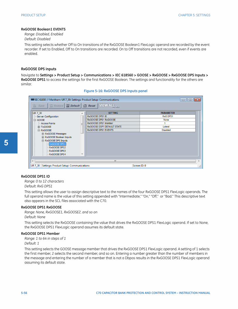
5-56 C70 CAPACITOR BANK PROTECTION AND CONTROL SYSTEM – INSTRUCTION MANUAL
PRODUCT SETUP CHAPTER 5: SETTINGS
5
RxGOOSE Boolean1 EVENTSRange: Disabled, EnabledDefault: Disabled
This setting selects whether Off to On transitions of the RxGOOSE Boolean1 FlexLogic operand are recorded by the event recorder. If set to Enabled, Off to On transitions are recorded. On to Off transitions are not recorded, even if events are enabled.
RxGOOSE DPS inputs
Navigate to Settings > Product Setup > Communications > IEC 618560 > GOOSE > RxGOOSE > RxGOOSE DPS Inputs > RxGOOSE DPS1 to access the settings for the first RxGOOSE Boolean. The settings and functionality for the others are similar.
Figure 5-16: RxGOOSE DPS Inputs panel
RxGOOSE DPS1 IDRange: 0 to 12 charactersDefault: RxG DPS1
This setting allows the user to assign descriptive text to the names of the four RxGOOSE DPS1 FlexLogic operands. The full operand name is the value of this setting appended with "Intermediate," "On," "Off," or "Bad." This descriptive text also appears in the SCL files associated with the C70.
RxGOOSE DPS1 RxGOOSERange: None, RxGOOSE1, RxGOOSE2, and so onDefault: None
This setting selects the RxGOOSE containing the value that drives the RxGOOSE DPS1 FlexLogic operand. If set to None, the RxGOOSE DPS1 FlexLogic operand assumes its default state.
RxGOOSE DPS1 MemberRange: 1 to 64 in steps of 1Default: 1
This setting selects the GOOSE message member that drives the RxGOOSE DPS1 FlexLogic operand. A setting of 1 selects the first member, 2 selects the second member, and so on. Entering a number greater than the number of members in the message and entering the number of a member that is not a Dbpos results in the RxGOOSE DPS1 FlexLogic operand assuming its default state.
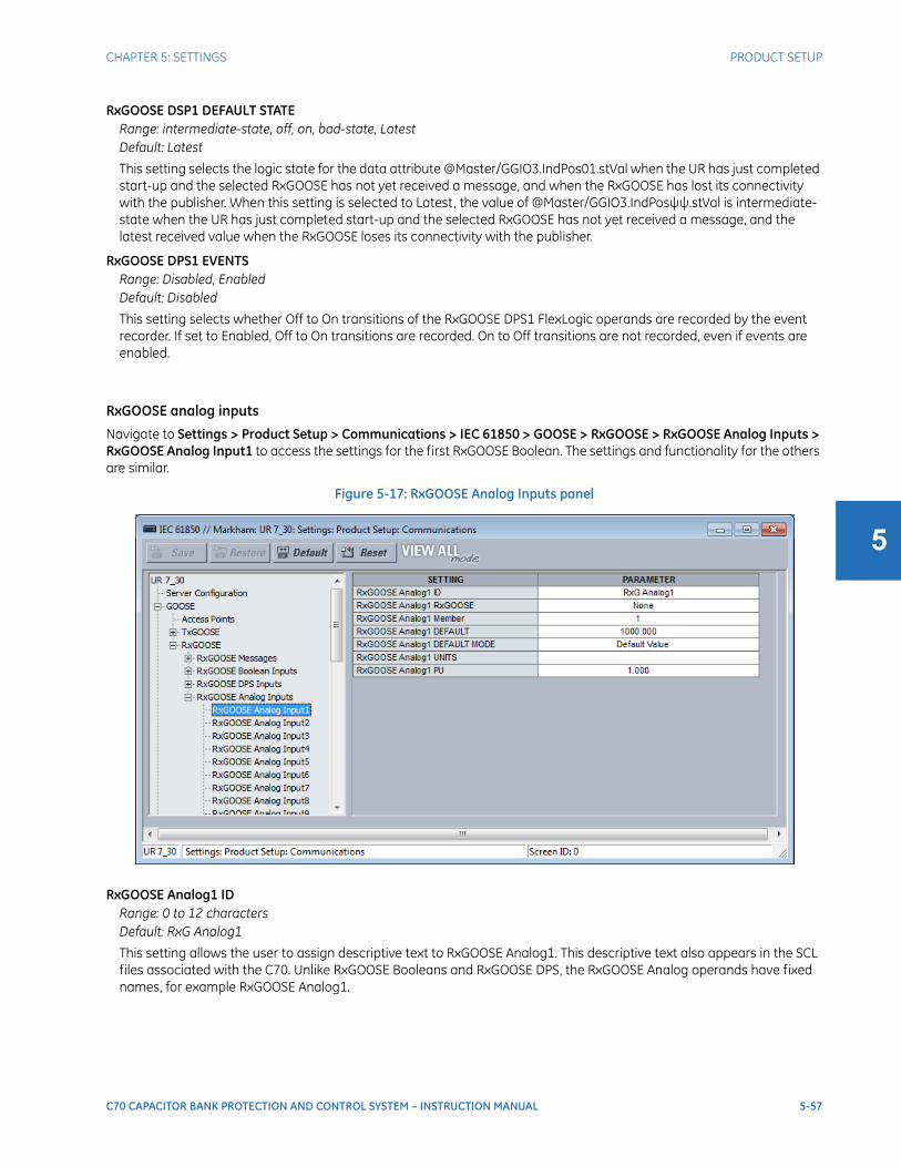
CHAPTER 5: SETTINGS PRODUCT SETUP
C70 CAPACITOR BANK PROTECTION AND CONTROL SYSTEM – INSTRUCTION MANUAL 5-57
5
RxGOOSE DSP1 DEFAULT STATERange: intermediate-state, off, on, bad-state, LatestDefault: Latest
This setting selects the logic state for the data attribute @Master/GGIO3.IndPos01.stVal when the UR has just completed start-up and the selected RxGOOSE has not yet received a message, and when the RxGOOSE has lost its connectivity with the publisher. When this setting is selected to Latest, the value of @Master/GGIO3.IndPosψψ.stVal is intermediate-state when the UR has just completed start-up and the selected RxGOOSE has not yet received a message, and the latest received value when the RxGOOSE loses its connectivity with the publisher.
RxGOOSE DPS1 EVENTSRange: Disabled, EnabledDefault: Disabled
This setting selects whether Off to On transitions of the RxGOOSE DPS1 FlexLogic operands are recorded by the event recorder. If set to Enabled, Off to On transitions are recorded. On to Off transitions are not recorded, even if events are enabled.
RxGOOSE analog inputs
Navigate to Settings > Product Setup > Communications > IEC 61850 > GOOSE > RxGOOSE > RxGOOSE Analog Inputs > RxGOOSE Analog Input1 to access the settings for the first RxGOOSE Boolean. The settings and functionality for the others are similar.
Figure 5-17: RxGOOSE Analog Inputs panel
RxGOOSE Analog1 IDRange: 0 to 12 charactersDefault: RxG Analog1
This setting allows the user to assign descriptive text to RxGOOSE Analog1. This descriptive text also appears in the SCL files associated with the C70. Unlike RxGOOSE Booleans and RxGOOSE DPS, the RxGOOSE Analog operands have fixed names, for example RxGOOSE Analog1.

5-58 C70 CAPACITOR BANK PROTECTION AND CONTROL SYSTEM – INSTRUCTION MANUAL
PRODUCT SETUP CHAPTER 5: SETTINGS
5
RxGOOSE Analog1 RxGOOSERange: None, RxGOOSE1, RxGOOSE2, and so onDefault: None
This setting selects the RxGOOSE containing the value that drives the RxGOOSE Analog1 FlexAnalog operand. If set to None, the RxGOOSE Analog1 FlexAnalog operand assumes its default state.
RxGOOSE Analog1 MemberRange: 1 to 64 in steps of 1Default: 1
This setting selects the GOOSE message member that drives the RxGOOSE Analog1 FlexAnalog operand. A setting of 1 selects the first member, 2 selects the second member, and so on. Entering a number greater than the number of members in the message and entering the number of a member that is not a FLOAT32 results in the RxGOOSE Analog1 FlexAnalog operand assuming its default state.
RxGOOSE Analog1 DEFAULTRange: -1000000.000 to 1000000.000 in steps of 0.001Default: 1000.000
This setting specifies the value of the GOOSE analog input when the selected RxGOOSE has lost its connectivity with the publisher and the RxGOOSE Analog1 DEFAULT MODE is set to "Default Value." Otherwise this setting has no effect. This setting is stored as an IEEE 754 / IEC 60559 floating point number. Because of the large range of this setting, not all possible values can be stored. Some values can be rounded to the closest possible floating point number.
RxGOOSE Analog1 DEFAULT MODERange: Default Value, Last KnownDefault: Default Value
When the selected RxGOOSE has lost its connectivity with the publisher and this setting is "Last Known," the value of the RxGOOSE Analog1 FlexLogic operand remains at the last received value. When the selected RxGOOSE has lost its connectivity with the publisher and this setting value is "Default Value," then the RxGOOSE Analog1 FlexLogic operand is defined by the RxGOOSE Analog1 DEFAULT setting. After restart, until a message is received, the operand value is the default value.
RxGOOSE Analog1 UNITSRange: up to 4 charactersDefault:
This setting specifies a four-character string that can is used in the actual values display of RxGOOSE Analog1.
RxGOOSE Analogs are floating-point values, with no units. The RxGOOSE UNIT and PU base settings allow the user to configure RxGOOSE Analog, so that it can be used in a FlexElement.
RxGOOSE Analogs that represent current, voltage, power, frequency, angles, or power factor can be used in a FlexElement. The following text must be used in the UNITS setting, to represent these types of analogs: A, V, W, var, VA, Hz, deg, and no text (blank setting) for power factor.
RxGOOSE Analogs can be compared to other RxGOOSE Analogs with any character string or no string.
RxGOOSE Analog1 PURange: 0.000 to 1000000000.000 in steps of 0.001Default: 1.000
This setting specifies the per-unit base value for other C70 features to use with the RxGOOSE Analog1 operand. A FlexElement for instance subtracts two quantities after converting their values to integers rescaled to a common base, the common base being the largest of the base values of the two quantities. If one of quantities is RxGOOSE Analog1 and its per-unit base value is not appropriate, the rescaling operation can result in unnecessary loss of precision or overflow in the integer result. The FlexElement Base Units table in the Settings > FlexLogic > FlexElements section later, which tabulates the per-unit base value used by its pickup setting and implies the per-unit base used by other FlexAnalogs, can be of use in selecting a value for the RxGOOSE Analog1 PU setting.
Some UR elements have requirements for the type of input operands, for instance current type or voltage type. These elements assume that RxGOOSE Analog operands are of whatever type is necessary to meet these requirements.
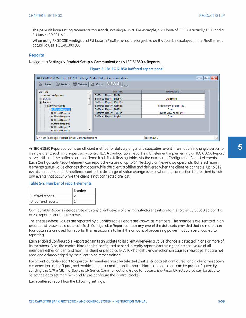
CHAPTER 5: SETTINGS PRODUCT SETUP
C70 CAPACITOR BANK PROTECTION AND CONTROL SYSTEM – INSTRUCTION MANUAL 5-59
5
The per-unit base setting represents thousands, not single units. For example, a PU base of 1.000 is actually 1000 and a PU base of 0.001 is 1.
When using RxGOOSE Analogs and PU base in FlexElements, the largest value that can be displayed in the FlexElement actual values is 2,140,000.000.
ReportsNavigate to Settings > Product Setup > Communications > IEC 61850 > Reports.
Figure 5-18: IEC 61850 buffered report panel
An IEC 61850 Report server is an efficient method for delivery of generic substation event information in a single server to a single client, such as a supervisory control IED. A Configurable Report is a UR element implementing an IEC 61850 Report server, either of the buffered or unbuffered kind. The following table lists the number of Configurable Report elements. Each Configurable Report element can report the values of up to 64 FlexLogic or FlexAnalog operands. Buffered report elements queue value changes that occur while the client is offline and delivered when the client re-connects. Up to 512 events can be queued. Unbuffered control blocks purge all value change events when the connection to the client is lost; any events that occur while the client is not connected are lost.
Table 5-9: Number of report elements
Configurable Reports interoperate with any client device of any manufacturer that conforms to the IEC 61850 edition 1.0 or 2.0 report client requirements.
The entities whose values are reported by a Configurable Report are known as members. The members are itemized in an ordered list known as a data set. Each Configurable Report can use any one of the data sets provided that no more than four data sets are used for reports. This restriction is to limit the amount of processing power that can be allocated to reporting.
Each enabled Configurable Report transmits an update to its client whenever a value change is detected in one or more of its members. Also, the control block can be configured to send integrity reports containing the present value of all members either on demand from the client or periodically. A TCP handshaking mechanism causes messages that are not read and acknowledged by the client to be retransmitted.
For a Configurable Report to operate, its members must be selected (that is, its data set configured) and a client must open a connection to, configure, and enable its report control block. Control blocks and data sets can be pre-configured by sending the C70 a CID file. See the UR Series Communications Guide for details. EnerVista UR Setup also can be used to select the data set members and to pre-configure the control blocks.
Each buffered report has the following settings.
Number
Buffered reports 20
Unbuffered reports 14

5-60 C70 CAPACITOR BANK PROTECTION AND CONTROL SYSTEM – INSTRUCTION MANUAL
PRODUCT SETUP CHAPTER 5: SETTINGS
5
Buffered Report1 RptIDRange: 0 to 129 VisibleString charactersDefault: empty string
The entered value sets the RptID value in Buffered Report1 messages, and it can be used by the client to discriminate Buffered Report1 messages from other messages. If the number of characters entered is zero, the value used for RptID in messages is an ObjectReference to the report's control block, that is, "<LDName>/LLN0$BR$"BRCB01".
Buffered Report1 DatSetRange: None, DataSet01, DataSet02, … Default: None
This setting selects the data set whose members' status is reported in Buffered Report1 messages using the UR Setup software designator for the data set. The IEC 61850 name of the data sets are configured in the Datasets panel, as described later.
An ObjectReference to the data set, which consists of the concatenation of the string "<LDName>/LLN0$" and the data set name, is used in the datSet field of report messages, and it can be used by the client to discriminate Buffered Report1 messages from other messages.
Buffered Report1 ConfRevRange: 0 to 4294967295 in steps of 1Default: 1
The entered value sets the confRev value in Buffered Report1 messages, and it can be used by clients to discriminate report messages of the expected configuration revision from messages of a different revision. The standard requires that confRef be incremented each time the members or the order of the members is changed, and each time the data set name is changed. The standard states that the value of 0 is reserved.
Buffered Report1 OptFldsRange: The check box for each individual bit can be enabled or not (see figure)Default: All bits true
The OptFlds setting is bitstring that controls which of the optional fields are included in report messages. The figure shows the available option bits.
Figure 5-19: Options for buffered report messages
Buffered Report1 BufTmRange: 0 to 4294967295 in steps of 1Default: 0
The entered value sets the time interval in milliseconds for the buffering of events for inclusion in a single report.

CHAPTER 5: SETTINGS PRODUCT SETUP
C70 CAPACITOR BANK PROTECTION AND CONTROL SYSTEM – INSTRUCTION MANUAL 5-61
5
Buffered Report1 TrgOpsRange: The check box for an individual bit can be enabled or notDefault: All bits true
The TrgOps setting is bitstring that controls which trigger conditions are monitored in this report. The options are as follows:
– data-change
– quality-change
– integrity
– general interrogation
Buffered Report1 IntgPdRange: 0 to 4294967295 in steps of 1Default: 0
The entered value sets the period in milliseconds for generating Buffered Report1 integrity reports. An integrity report includes the values of all members of the referenced data set, whether a change has occurred or not.
Each unbuffered report has the following settings.
Unbuffered Report1 RptIDRange: 0 to 129 VisibleString charactersDefault:
The entered value sets the RptID value in Unbuffered Report1 messages, and it can be used by the client to discriminate Unbuffered Report1 messages from other messages. If the number of characters entered is zero, the value used for RptID in messages is an ObjectReference to the report's control block, that is, "<LDName>/LLN0$RP$"URCB01".
Unbuffered Report1 DatSetRange: None, DataSet01, DataSet02, …Default: None
This setting selects the data set whose members' status is reported in Unbuffered Report1 messages using the UR Setup software designator for the data set. The IEC 61850 name of the data sets are configured in the Datasets panel, as described later.
An ObjectReference to the data set, which consists of the concatenation of the string "<LDName>/LLN0$" and the data set name, is used in the datSet field of report messages, and it can be used by the client to discriminate Unbuffered Report1 messages from other messages.
Unbuffered Report1 ConfRevRange: 0 to 4294967295 in steps of 1Default: 0
The entered value sets the confRev value in Unbuffered Report1 messages, and it can be used by clients to discriminate report messages of the expected configuration revision from messages of a different revision. The standard requires that confRef be incremented each time the members or the order of the members is changed, and each time the data set name is changed.
Unbuffered Report1 OptFldsRange: The check box for an individual bit can be enabled or notDefault: All bits true
The OptFlds setting is bitstring that controls which of the optional fields are included in report messages. The options are as follows:
– sequence-number
– report-time-stamp
– reason-for-inclusion
– data-set-name
– data-reference
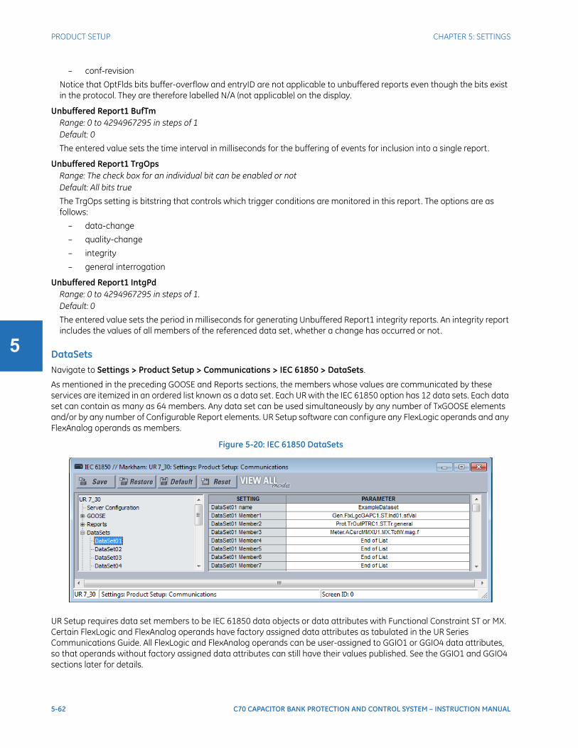
5-62 C70 CAPACITOR BANK PROTECTION AND CONTROL SYSTEM – INSTRUCTION MANUAL
PRODUCT SETUP CHAPTER 5: SETTINGS
5
– conf-revision
Notice that OptFlds bits buffer-overflow and entryID are not applicable to unbuffered reports even though the bits exist in the protocol. They are therefore labelled N/A (not applicable) on the display.
Unbuffered Report1 BufTmRange: 0 to 4294967295 in steps of 1Default: 0
The entered value sets the time interval in milliseconds for the buffering of events for inclusion into a single report.
Unbuffered Report1 TrgOpsRange: The check box for an individual bit can be enabled or notDefault: All bits true
The TrgOps setting is bitstring that controls which trigger conditions are monitored in this report. The options are as follows:
– data-change
– quality-change
– integrity
– general interrogation
Unbuffered Report1 IntgPdRange: 0 to 4294967295 in steps of 1.Default: 0
The entered value sets the period in milliseconds for generating Unbuffered Report1 integrity reports. An integrity report includes the values of all members of the referenced data set, whether a change has occurred or not.
DataSetsNavigate to Settings > Product Setup > Communications > IEC 61850 > DataSets.
As mentioned in the preceding GOOSE and Reports sections, the members whose values are communicated by these services are itemized in an ordered list known as a data set. Each UR with the IEC 61850 option has 12 data sets. Each data set can contain as many as 64 members. Any data set can be used simultaneously by any number of TxGOOSE elements and/or by any number of Configurable Report elements. UR Setup software can configure any FlexLogic operands and any FlexAnalog operands as members.
Figure 5-20: IEC 61850 DataSets
UR Setup requires data set members to be IEC 61850 data objects or data attributes with Functional Constraint ST or MX. Certain FlexLogic and FlexAnalog operands have factory assigned data attributes as tabulated in the UR Series Communications Guide. All FlexLogic and FlexAnalog operands can be user-assigned to GGIO1 or GGIO4 data attributes, so that operands without factory assigned data attributes can still have their values published. See the GGIO1 and GGIO4 sections later for details.

CHAPTER 5: SETTINGS PRODUCT SETUP
C70 CAPACITOR BANK PROTECTION AND CONTROL SYSTEM – INSTRUCTION MANUAL 5-63
5
Datasets used by TxGOOSE1, TxGOOSE2, and/or by reports also provide a chatter suppression service for their Boolean members. Oscillation in a value, also known as chatter, can be caused by errors in logic programming, inadequate hysteresis (deadband) on a threshold, or a failed station component. Chatter can flood a communications network with GOOSE messages, degrading response time for all users. If chatter is detected in a Boolean member, TxGOOSE suspends GOOSE event message triggering and report message triggering from that member for as long as the condition exists, and for a minimum period of one second. While sending is suspended, a self-test message identifying the specific data item detected as oscillating is activated.
Navigate to Settings > Product Setup > Communications > IEC 61850 > DataSets > DataSet01 to access the settings for the first data set. The settings and functionality for the others are similar.
DataSet01 nameRange: 0 to 32 VisibleString charactersDefault: DataSet01
The value entered sets the name of the data set, which is required to be unique within the UR for proper operation. An ObjectReference to the data set consists of a string that is the concatenation of "<LDName>/LLN0$" and the DataSet01 name setting value. An ObjectReference to the data set is published in the datSet field of TxGOOSE messages, and it can be used by subscribers to discriminate the messages of that TxGOOSE from other GOOSE messages. An ObjectReference to the data set is optionally published in the DatSet field of Report messages. Valid characters are upper and lowercase letters, digits, and the underscore (_) character. The first character must be a letter.
DataSet01 Member1Range: End of List or any instantiated 61850 data object or data attribute with Functional Constraint ST or MXDefault: End of List
This setting specifies the first member in TxGOOSE1 messages. There is a similar setting for each of the up to 64 members that the UR allows in a Dataset. Only values of members before the first set to End of List are published.
Deadband settingsA deadband is a range in which no action occurs, expressed as a percentage.
The IEC 61850 panels contain hundreds of deadband settings, such as in the following panels: System Setup > Signal Sources, FlexLogic, Grouped Elements, Control Elements, and GGIO4. Each panel is not outlined here.
Deadband setting names all end either with "DEADBAND" or .db. As they all work the same way, but each on a different analog value, a single description applicable to all deadband settings is given here. The analog value that each deadband setting applies to is usually obvious from the name of the setting. However, a tabulation of the analog values and their associated deadband setting can be found in the UR Series Communications Guide.
Figure 5-21: Deadband settings with .db suffix
GOOSE, buffered report, and unbuffered report messages are for the most part transmitted only when there is a value change in one or more of their members. Most analog values continuously dither by an amount that is not significant. Were a report to be sent each time an insignificant analog value change occurred, then the communications network floods with GOOSE and report messages, degrading response time for all users.
To control this, a deadband setting is provided for each analog value. Also, in addition to the present actual value of each analog ("instMag" in the following figure), there is a deadbanded value ("mag" in the figure), which is updated with the present value only when the difference between the two exceeds the deadband setting (db in the figure). Changes to this deadbanded value trigger transmissions when included in GOOSE and report data sets.

5-64 C70 CAPACITOR BANK PROTECTION AND CONTROL SYSTEM – INSTRUCTION MANUAL
PRODUCT SETUP CHAPTER 5: SETTINGS
5
Figure 5-22: Deadband settings
Deadband settings are entered in UR Setup in units of percent of the difference between the "max." and "min." of the associated analog value. A zero deadband setting suppresses transmission triggering. The range of deadband settings is 0.000 to 100.000% in steps of 0.001. The default value is 10.000%.
GGIO4 elements have individual settings for "min." and "max." The min. and max. for FlxEIGAPC#.OpSig.db (FLEXELEMENT # OpSig) are -50 pu and +50 pu respectively. The min. value for all other quantities is 0. The max. values are as follows:
• Phase current — 46 x phase CT primary setting
• Neutral current — 46 x ground CT primary setting
• Phase and phase-to-phase voltage — 275 x VT ratio setting
• Power (real, reactive, apparent, 3-phase, and 1-phase) — 46 x phase CT primary setting x 275 x VT ratio setting
• Energy (real or imaginary) — 46 x phase CT primary setting x 275 x VT ratio setting x 1 hour
• Frequency — 90 Hz
• Frequency rate of change — 90 Hz/s
• Power factor — 2
• Angle — 360 degrees
Select the deadband settings from knowledge of the characteristics of the power system quantity measured and knowledge of the demands of the applications receiving the measurement via GOOSE or report such that changes of significance to the application are promptly reported, yet the network is not overly burdened with event messages.
Breaker 1The UR breaker control and status monitoring elements have certain settings that configure how the IEC 61850 protocol interacts with these elements. These settings are described in this section. See the Breakers section in the System Setup section of this chapter for details on the operation of breaker control elements.
Navigate to Settings > Communications > IEC 61850 > System Setup > Breakers > Breaker 1 to access the settings that configure the IEC 61850 protocol interface with the first breaker control and status monitoring element. The settings and functionality for the others are similar.
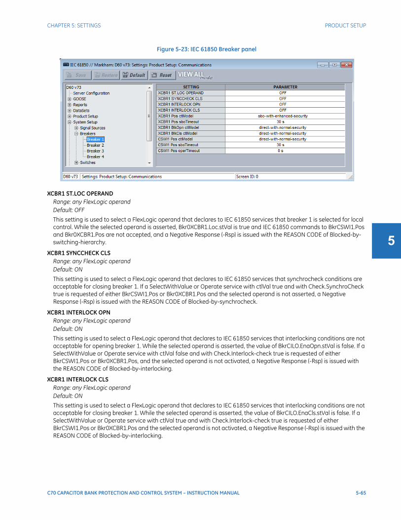
CHAPTER 5: SETTINGS PRODUCT SETUP
C70 CAPACITOR BANK PROTECTION AND CONTROL SYSTEM – INSTRUCTION MANUAL 5-65
5
Figure 5-23: IEC 61850 Breaker panel
XCBR1 ST.LOC OPERANDRange: any FlexLogic operandDefault: OFF
This setting is used to select a FlexLogic operand that declares to IEC 61850 services that breaker 1 is selected for local control. While the selected operand is asserted, Bkr0XCBR1.Loc.stVal is true and IEC 61850 commands to BkrCSWI1.Pos and Bkr0XCBR1.Pos are not accepted, and a Negative Response (-Rsp) is issued with the REASON CODE of Blocked-by-switching-hierarchy.
XCBR1 SYNCCHECK CLSRange: any FlexLogic operandDefault: ON
This setting is used to select a FlexLogic operand that declares to IEC 61850 services that synchrocheck conditions are acceptable for closing breaker 1. If a SelectWithValue or Operate service with ctlVal true and with Check.SynchroCheck true is requested of either BkrCSWI1.Pos or Bkr0XCBR1.Pos and the selected operand is not asserted, a Negative Response (-Rsp) is issued with the REASON CODE of Blocked-by-synchrocheck.
XCBR1 INTERLOCK OPNRange: any FlexLogic operandDefault: ON
This setting is used to select a FlexLogic operand that declares to IEC 61850 services that interlocking conditions are not acceptable for opening breaker 1. While the selected operand is asserted, the value of BkrCILO.EnaOpn.stVal is false. If a SelectWithValue or Operate service with ctlVal false and with Check.Interlock-check true is requested of either BkrCSWI1.Pos or Bkr0XCBR1.Pos, and the selected operand is not activated, a Negative Response (-Rsp) is issued with the REASON CODE of Blocked-by-interlocking.
XCBR1 INTERLOCK CLSRange: any FlexLogic operandDefault: ON
This setting is used to select a FlexLogic operand that declares to IEC 61850 services that interlocking conditions are not acceptable for closing breaker 1. While the selected operand is asserted, the value of BkrCILO.EnaCls.stVal is false. If a SelectWithValue or Operate service with ctlVal true and with Check.Interlock-check true is requested of either BkrCSWI1.Pos or Bkr0XCBR1.Pos and the selected operand is not activated, a Negative Response (-Rsp) is issued with the REASON CODE of Blocked-by-interlocking.

5-66 C70 CAPACITOR BANK PROTECTION AND CONTROL SYSTEM – INSTRUCTION MANUAL
PRODUCT SETUP CHAPTER 5: SETTINGS
5
XCBR1 Pos ctlModelRange: status-only, direct-with-normal-security, sbo-with-normal-security, direct-with-enhanced-security, sbo-with-enhanced-securityDefault: sbo-with-enhanced-security
This setting selects the control model clients must use to successfully control the breaker 1 signals marked Bkr0XCBR1.PosOpn.ctlVal and Bkr0XCBR1.PosCls.ctlVal on the Breaker Control Logic (Sheet 1 of 2) diagram in the Settings > System Setup section later in this chapter. These signals force a breaker 1 three-phase trip or close control while the operand selected by setting XCBR1 ST.LOC OPERAND is not active.
"sbo" here is select-before-operate. Enhanced security means that the UR reports to the client the breaker 1 position at the end of the command sequence.
XCBR1 Pos sboTimeoutRange: 2.000 to 60.000 s in steps of 0.001sDefault: 30.000 s
This setting specifies the maximum time between a select and an operate command to breaker 1 signals marked Bkr0XCBR1.PosOpn.ctlVal and Bkr0XCBR1.PosCls.ctlVal in order for the operand to be successful. This setting is only relevant when XCBR1 Pos ctlModel is sbo-with-normal-security or sbo-with-enhanced-security.
XCBR1 BlkOpn ctlModelRange: status-only, direct-with-normal-security, sbo-with-normal-securityDefault: direct-with-normal-security
This setting selects the control model clients must use to successfully control the breaker 1 signal marked Bkr0XCBR1.BlkOpn.ctlVal signal on the Breaker Control Logic (Sheet 1 of 2) diagram in the Settings > System Setup section later. This signal when true blocks breaker 1 trip control while the operand selected by setting XCBR1 ST.LOC OPERAND is not active.
XCBR1 BlkCls ctlModelRange: status-only, direct-with-normal-security, sbo-with-normal-securityDefault: direct-with-normal-security
This setting selects the control model clients must use to successfully control the breaker 1 signal marked Bkr0XCBR1.BlkCls.ctlVal signal on the Breaker Control Logic (Sheet 1 of 2) diagram in the Settings > System Setup section later. This signal when true blocks breaker 1 close control while the operand selected by setting XCBR1 ST.LOC OPERAND is not active.
CSWI1 Pos ctlModelRange: status-only, direct-with-normal-security, sbo-with-normal-security, direct-with-enhanced-security, sbo-with-enhanced-securityDefault: direct-with-normal-security
This setting selects the control model clients must use to successfully control the breaker 1 signals marked BkrCSWI1.PosOpn.ctlVal and BkrCSWI1.PosCls.ctlVal on the Breaker Control Logic (Sheet 1 of 2) diagram in the Settings > System Setup section earlier. These signals force a breaker 1 three-phase trip or close control while the operand selected by setting XCBR1 ST.LOC OPERAND is not active.
CSWI1 Pos sboTimeoutRange: 2.000 to 60.000 s in steps of 0.001sDefault: 30.000 s
This setting specifies the maximum time between a select and an operate command to breaker 1 via BkrCSWI1.Pos in order for the operand to be successful. This setting is only relevant when CSWI1 Pos ctlModel is sbo-with-normal-security or sbo-with-enhanced-security.
CSWI1 Pos operTimeoutRange: 0.000 to 2.000 s in steps of 0.001sDefault: 0.100 s
This setting specifies the maximum time between an operate command to breaker 1 via BkrCSWI1.Pos until BkrCSWI1.Pos.stVal enters the commanded state. The command terminates if the commanded state is not reached in the set time.
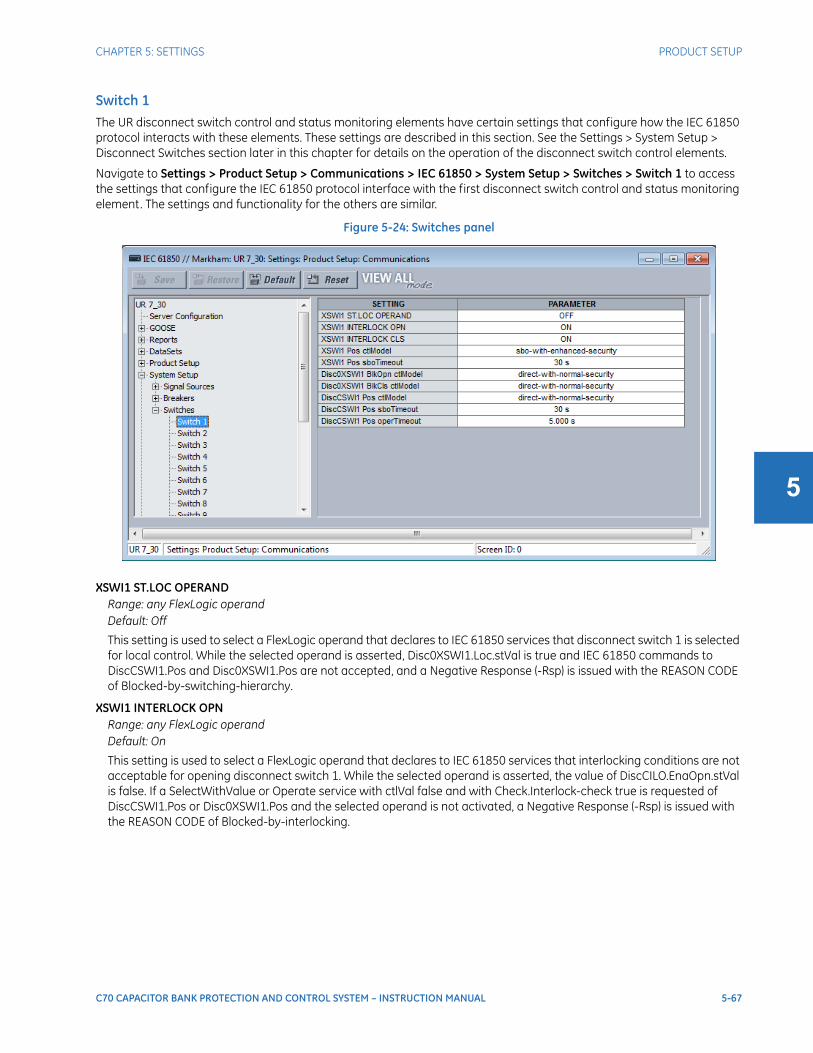
CHAPTER 5: SETTINGS PRODUCT SETUP
C70 CAPACITOR BANK PROTECTION AND CONTROL SYSTEM – INSTRUCTION MANUAL 5-67
5
Switch 1The UR disconnect switch control and status monitoring elements have certain settings that configure how the IEC 61850 protocol interacts with these elements. These settings are described in this section. See the Settings > System Setup > Disconnect Switches section later in this chapter for details on the operation of the disconnect switch control elements.
Navigate to Settings > Product Setup > Communications > IEC 61850 > System Setup > Switches > Switch 1 to access the settings that configure the IEC 61850 protocol interface with the first disconnect switch control and status monitoring element. The settings and functionality for the others are similar.
Figure 5-24: Switches panel
XSWI1 ST.LOC OPERANDRange: any FlexLogic operandDefault: Off
This setting is used to select a FlexLogic operand that declares to IEC 61850 services that disconnect switch 1 is selected for local control. While the selected operand is asserted, Disc0XSWI1.Loc.stVal is true and IEC 61850 commands to DiscCSWI1.Pos and Disc0XSWI1.Pos are not accepted, and a Negative Response (-Rsp) is issued with the REASON CODE of Blocked-by-switching-hierarchy.
XSWI1 INTERLOCK OPNRange: any FlexLogic operandDefault: On
This setting is used to select a FlexLogic operand that declares to IEC 61850 services that interlocking conditions are not acceptable for opening disconnect switch 1. While the selected operand is asserted, the value of DiscCILO.EnaOpn.stVal is false. If a SelectWithValue or Operate service with ctlVal false and with Check.Interlock-check true is requested of DiscCSWI1.Pos or Disc0XSWI1.Pos and the selected operand is not activated, a Negative Response (-Rsp) is issued with the REASON CODE of Blocked-by-interlocking.

5-68 C70 CAPACITOR BANK PROTECTION AND CONTROL SYSTEM – INSTRUCTION MANUAL
PRODUCT SETUP CHAPTER 5: SETTINGS
5
XSWI1 INTERLOCK CLSRange: any FlexLogic operandDefault: On
This setting is used to select a FlexLogic operand that declares to IEC 61850 services that interlocking conditions are not acceptable for closing disconnect switch 1. While the selected operand is asserted, the value of DiscCILO.EnaCls.stVal is false. If a SelectWithValue or Operate service with ctlVal true and with Check.Interlock-check true is requested of DiscCSWI1.Pos or Disc0XSWI1.Pos and the selected operand is not activated, a Negative Response (-Rsp) is issued with the REASON CODE of Blocked-by-interlocking.
XSWI1 Pos ctlModelRange: status-only, direct-with-normal-security, sbo-with-normal-security, direct-with-enhanced-security, sbo-with-enhanced-securityDefault: sbo-with-enhanced-security
This setting selects the control model that clients must use to successfully control the disconnect switch 1 signals marked Disc0XCBR1.PosOpn.ctlVal and Disc0XCBR1.PosCls.ctlVal on the Disconnect Switch Logic diagram in the Settings > System Setup section later. These signals force a disconnect switch trip or close control while the operand selected by setting XSWI1 ST.LOC OPERAND is not active.
"sbo" here is select-before-operate. Enhanced security means that the C70 reports to the client the disconnect switch 1 position the end of the command sequence.
XSWI1 Pos sboTimeoutRange: 2.000 to 60.000 s in steps of 0.001sDefault: 30.000 s
This setting specifies the maximum time between a select and an operate command to disconnect switch 1 signals marked Disc0XCBR1.PosOpn.ctlVal and Disc0XCBR1.PosCls.ctlVal in order for the operand to be successful. This setting is only relevant when XSWI1 Pos ctlModel is sbo-with-normal-security or sbo-with-enhanced-security.
XSWI1 BlkOpn ctlModelRange: status-only, direct-with-normal-security, sbo-with-normal-securityDefault: sbo-with-normal-security
This setting selects the control model clients must use to successfully control the disconnect switch 1 signal marked DiscCSWI1.BlkOpn.ctlVal signal on the Disconnect Switch Logic diagram in the Settings > System Setup section later. This signal when true blocks disconnect switch 1 trip control while the operand selected by setting XSWI1 ST.LOC OPERAND is not active.
XSWI1 BlkCls ctlModelRange: status-only, direct-with-normal-security, sbo-with-normal-securityDefault: sbo-with-normal-security
This setting selects the control model clients must use to successfully control the disconnect switch 1 signal marked DiscCSWI1.BlkCls.ctlVal signal on the Disconnect Switch Logic diagram in the Settings > System Setup section later. This signal when true blocks disconnect switch 1 close control while the operand selected by setting XSWI1 ST.LOC OPERAND is not active.
CSWI1 Pos ctlModelRange: status-only, direct-with-normal-security, sbo-with-normal-security, direct-with-enhanced-security, sbo-with-enhanced-securityDefault: sbo-with-normal-security
This setting selects the control model clients must use to successfully control the disconnect switch 1 signals marked DiscCSWI1.PosOpn.ctlVal and DiscCSWI1.PosCls.ctlVal on the Disconnect Switch Logic diagram in the Settings > System Setup section later. These signals force a disconnect switch trip or close control while the operand selected by setting XSWI1 ST.LOC OPERAND is not active.
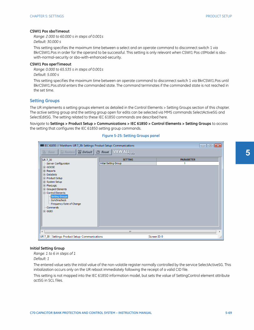
CHAPTER 5: SETTINGS PRODUCT SETUP
C70 CAPACITOR BANK PROTECTION AND CONTROL SYSTEM – INSTRUCTION MANUAL 5-69
5
CSWI1 Pos sboTimeoutRange: 2.000 to 60.000 s in steps of 0.001sDefault: 30.000 s
This setting specifies the maximum time between a select and an operate command to disconnect switch 1 via BkrCSWI1.Pos in order for the operand to be successful. This setting is only relevant when CSWI1 Pos ctlModel is sbo-with-normal-security or sbo-with-enhanced-security.
CSWI1 Pos operTimeoutRange: 0.000 to 65.535 s in steps of 0.001sDefault: 5.000 s
This setting specifies the maximum time between an operate command to disconnect switch 1 via BkrCSWI1.Pos until BkrCSWI1.Pos.stVal enters the commanded state. The command terminates if the commanded state is not reached in the set time.
Setting GroupsThe UR implements a setting groups element as detailed in the Control Elements > Setting Groups section of this chapter. The active setting group and the setting group open for edits can be selected via MMS commands SelectActiveSG and SelectEditSG. The setting related to these IEC 61850 commands are described here.
Navigate to Settings > Product Setup > Communications > IEC 61850 > Control Elements > Setting Groups to access the setting that configures the IEC 61850 setting group commands.
Figure 5-25: Setting Groups panel
Initial Setting GroupRange: 1 to 6 in steps of 1Default: 1
The entered value sets the initial value of the non-volatile register normally controlled by the service SelectActiveSG. This initialization occurs only on the UR reboot immediately following the receipt of a valid CID file.
This setting is not mapped into the IEC 61850 information model, but sets the value of SettingControl element attribute actSG in SCL files.

5-70 C70 CAPACITOR BANK PROTECTION AND CONTROL SYSTEM – INSTRUCTION MANUAL
PRODUCT SETUP CHAPTER 5: SETTINGS
5
CommandsThe UR implements a number of clear records commands as detailed in the Commands and Targets chapter of this manual. Several of these commands also can be issued via IEC 61850. The settings related to these IEC 61850 commands are described here.
Navigate to Settings > Product Setup > Communications > IEC 61850 > Commands to access the settings that configure the IEC 61850 protocol interface for record clear commands.
Figure 5-26: Commands panel
FltRptRFLO1.RsStat.ctlModelRange: direct-with-normal-security, sbo-with-normal-securityDefault: direct-with-normal-security
This setting selects the control model clients must use to successfully control the command CLEAR FAULT REPORTS. "sbo" here is select-before-operate. Enhanced security means that the C70 reports to the client the breaker 1 position at the end of the command sequence.
LLN0.EvtRcdClr.ctlModelRange: direct-with-normal-security, sbo-with-normal-securityDefault: direct-with-normal-security
This setting selects the control model clients must use to successfully control the command CLEAR EVENT RECORDS.
LPHD1.RsStat.ctlModelRange: direct-with-normal-security, sbo-with-normal-securityDefault: direct-with-normal-security
This setting selects the control model clients must use to successfully control the command CLEAR ALL RELAY RECORDS.
OscRDRE1.RcdTrg.ctlModelRange: direct-with-normal-security, sbo-with-normal-securityDefault: direct-with-normal-security
This setting selects the control model clients must use to successfully control the command FORCE TRIGGER.

CHAPTER 5: SETTINGS PRODUCT SETUP
C70 CAPACITOR BANK PROTECTION AND CONTROL SYSTEM – INSTRUCTION MANUAL 5-71
5
OscRDRE1.MemClr.ctlModelRange: direct-with-normal-security, sbo-with-normal-securityDefault: direct-with-normal-security
This setting selects the control model clients must use to successfully control the command CLEAR OSCILLOGRAPHY.
DatLogRDRE1.MemClr.ctlModelRange: direct-with-normal-security, sbo-with-normal-securityDefault: direct-with-normal-security
This setting selects the control model clients must use to successfully control the command CLEAR DATA LOGGER.
EnrMtrMMTR.RsStat.ctlModelRange: direct-with-normal-security, sbo-with-normal-securityDefault: direct-with-normal-security
This setting selects the control model clients must use to successfully control the command CLEAR ENERGY.
GGIO1GGIO1 is a UR feature that allows up to 128 UR FlexLogic operands to be user-mapped to IEC 61850 information model data attributes.
For the value of a FlexLogic operand to be read via MMS, included in TxGOOSE messages, or included in buffered/unbuffered reports, the value must be assigned to a data attribute. GGIO1 allows those FlexLogic operands that have not yet been factory-assigned to a data attribute to be user-assigned to a generic data attribute, and thus have their values included in IEC 61850 communications.
Navigate to Settings > Product Setup > Communications > IEC 61850 > GGIO > GGIO1 to access the settings for GGIO1.
Figure 5-27: IEC 61850 GGIO1 panel
GGIO1 INDICATION 1Range: any FlexLogic operandDefault: OFF
This setting selects the FlexLogic operand whose value is mapped into the IEC 61850 data attribute <LDName>/GGIO1.Ind001.stVal. See the FlexLogic section in this chapter for a list of FlexLogic operands.
GGIO1 INDICATION 2Range: any FlexLogic operandDefault: OFF
Selects the FlexLogic operand mapped to <LDName>/GGIO1.Ind002.stVal, and so on.
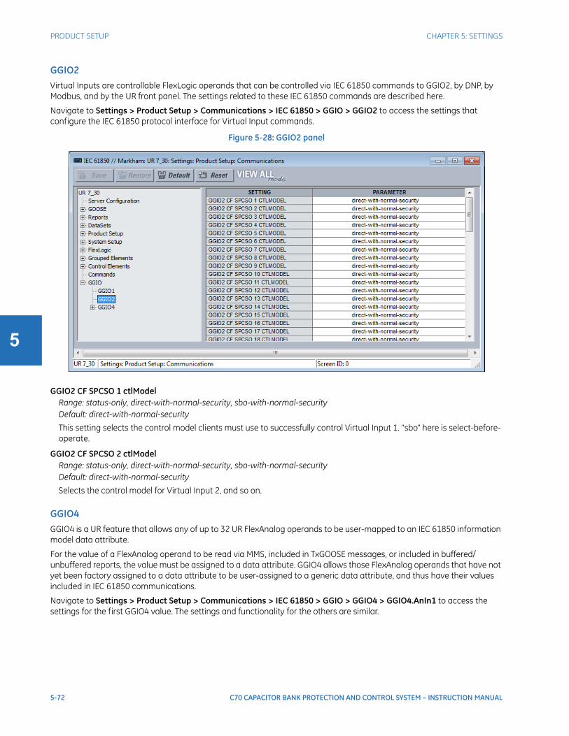
5-72 C70 CAPACITOR BANK PROTECTION AND CONTROL SYSTEM – INSTRUCTION MANUAL
PRODUCT SETUP CHAPTER 5: SETTINGS
5
GGIO2Virtual Inputs are controllable FlexLogic operands that can be controlled via IEC 61850 commands to GGIO2, by DNP, by Modbus, and by the UR front panel. The settings related to these IEC 61850 commands are described here.
Navigate to Settings > Product Setup > Communications > IEC 61850 > GGIO > GGIO2 to access the settings that configure the IEC 61850 protocol interface for Virtual Input commands.
Figure 5-28: GGIO2 panel
GGIO2 CF SPCSO 1 ctlModelRange: status-only, direct-with-normal-security, sbo-with-normal-securityDefault: direct-with-normal-security
This setting selects the control model clients must use to successfully control Virtual Input 1. "sbo" here is select-before-operate.
GGIO2 CF SPCSO 2 ctlModelRange: status-only, direct-with-normal-security, sbo-with-normal-securityDefault: direct-with-normal-security
Selects the control model for Virtual Input 2, and so on.
GGIO4GGIO4 is a UR feature that allows any of up to 32 UR FlexAnalog operands to be user-mapped to an IEC 61850 information model data attribute.
For the value of a FlexAnalog operand to be read via MMS, included in TxGOOSE messages, or included in buffered/unbuffered reports, the value must be assigned to a data attribute. GGIO4 allows those FlexAnalog operands that have not yet been factory assigned to a data attribute to be user-assigned to a generic data attribute, and thus have their values included in IEC 61850 communications.
Navigate to Settings > Product Setup > Communications > IEC 61850 > GGIO > GGIO4 > GGIO4.AnIn1 to access the settings for the first GGIO4 value. The settings and functionality for the others are similar.
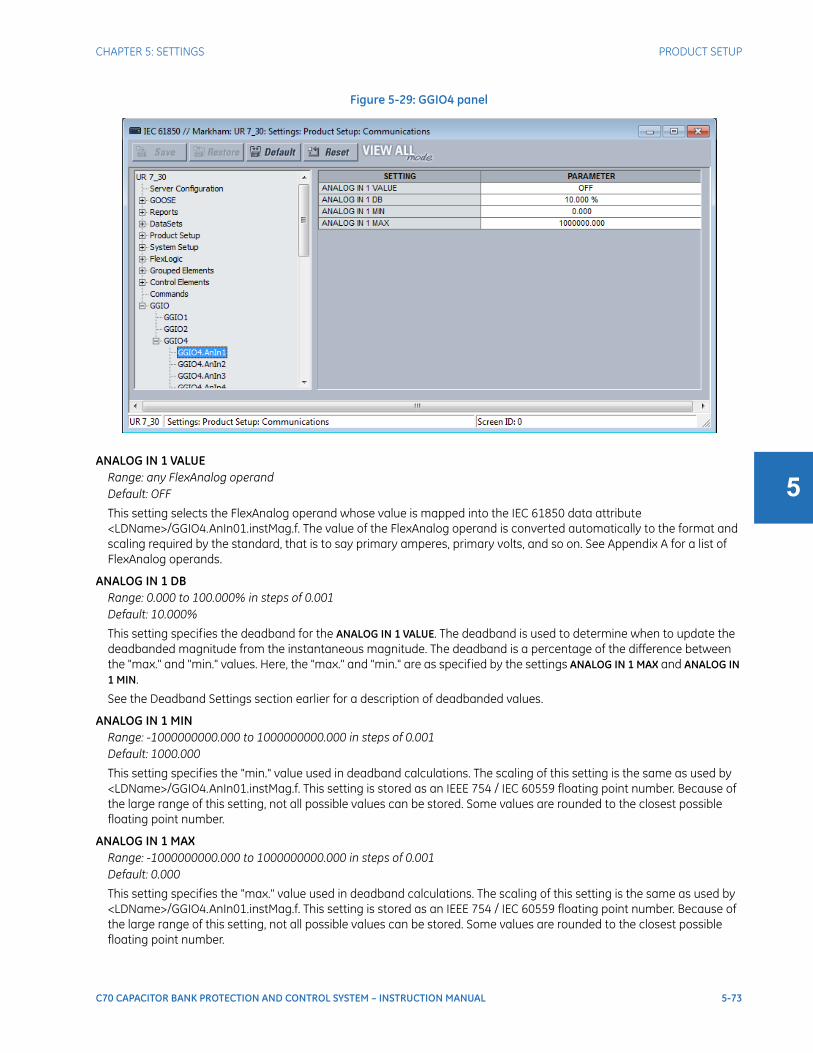
CHAPTER 5: SETTINGS PRODUCT SETUP
C70 CAPACITOR BANK PROTECTION AND CONTROL SYSTEM – INSTRUCTION MANUAL 5-73
5
Figure 5-29: GGIO4 panel
ANALOG IN 1 VALUERange: any FlexAnalog operandDefault: OFF
This setting selects the FlexAnalog operand whose value is mapped into the IEC 61850 data attribute <LDName>/GGIO4.AnIn01.instMag.f. The value of the FlexAnalog operand is converted automatically to the format and scaling required by the standard, that is to say primary amperes, primary volts, and so on. See Appendix A for a list of FlexAnalog operands.
ANALOG IN 1 DBRange: 0.000 to 100.000% in steps of 0.001Default: 10.000%
This setting specifies the deadband for the ANALOG IN 1 VALUE. The deadband is used to determine when to update the deadbanded magnitude from the instantaneous magnitude. The deadband is a percentage of the difference between the "max." and "min." values. Here, the "max." and "min." are as specified by the settings ANALOG IN 1 MAX and ANALOG IN 1 MIN.
See the Deadband Settings section earlier for a description of deadbanded values.
ANALOG IN 1 MINRange: -1000000000.000 to 1000000000.000 in steps of 0.001Default: 1000.000
This setting specifies the "min." value used in deadband calculations. The scaling of this setting is the same as used by <LDName>/GGIO4.AnIn01.instMag.f. This setting is stored as an IEEE 754 / IEC 60559 floating point number. Because of the large range of this setting, not all possible values can be stored. Some values are rounded to the closest possible floating point number.
ANALOG IN 1 MAXRange: -1000000000.000 to 1000000000.000 in steps of 0.001Default: 0.000
This setting specifies the "max." value used in deadband calculations. The scaling of this setting is the same as used by <LDName>/GGIO4.AnIn01.instMag.f. This setting is stored as an IEEE 754 / IEC 60559 floating point number. Because of the large range of this setting, not all possible values can be stored. Some values are rounded to the closest possible floating point number.

5-74 C70 CAPACITOR BANK PROTECTION AND CONTROL SYSTEM – INSTRUCTION MANUAL
PRODUCT SETUP CHAPTER 5: SETTINGS
5
File transfer by IEC 61850The C70 supports file transfer by IEC 61850. The approach is as follows, using the SISCO AX-S4 61850 client software as an example.
1. In the AX-S4 61850 Explorer window, click the Tools menu and access the SISCO File Transfer Utility.
2. Select the Remote AR Name from the drop-down list. Available files appear in the File Specification area on the right side of the window.
3. With the Copy option active, select a file to transfer and click the Go button. The file is copied and displays in the Local list on the left side of the window.
4. Repeat the process to transfer any other files.
Figure 5-30: File transfer by IEC 61850
5.3.4.13 Web server HTTP protocolSETTINGS PRODUCT SETUP COMMUNICATIONS WEB SERVER HTTP PROTOCOL
The C70 contains an embedded web server and can display pages in a web browser. The web pages are organized as a series of menus that can be accessed starting at the C70 “Main Menu.” Web pages are read-only and are available showing DNP and IEC 60870-5-104 points lists, Modbus registers, event records, fault reports, and so on. First connect the C70 and a computer to an Ethernet network, then enter the IP address of the C70 Ethernet port in a web browser.
To close the port, set the port number to 0. The change takes effect when the C70 is restarted.
WEB SERVER HTTP PROTOCOL HTTP TCP PORT
NUMBER: 80Range: 0 to 65535 in steps of 1
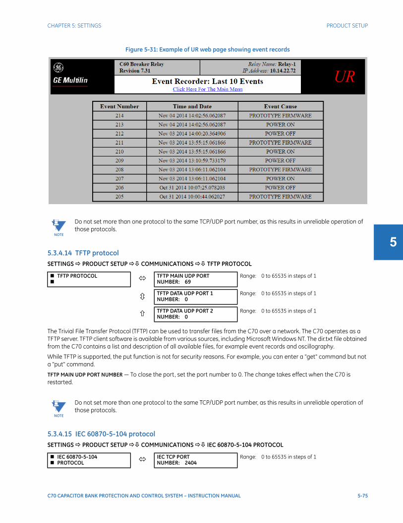
CHAPTER 5: SETTINGS PRODUCT SETUP
C70 CAPACITOR BANK PROTECTION AND CONTROL SYSTEM – INSTRUCTION MANUAL 5-75
5
Figure 5-31: Example of UR web page showing event records
5.3.4.14 TFTP protocolSETTINGS PRODUCT SETUP COMMUNICATIONS TFTP PROTOCOL
The Trivial File Transfer Protocol (TFTP) can be used to transfer files from the C70 over a network. The C70 operates as a TFTP server. TFTP client software is available from various sources, including Microsoft Windows NT. The dir.txt file obtained from the C70 contains a list and description of all available files, for example event records and oscillography.
While TFTP is supported, the put function is not for security reasons. For example, you can enter a "get" command but not a "put" command.
TFTP MAIN UDP PORT NUMBER — To close the port, set the port number to 0. The change takes effect when the C70 is restarted.
5.3.4.15 IEC 60870-5-104 protocolSETTINGS PRODUCT SETUP COMMUNICATIONS IEC 60870-5-104 PROTOCOL
NOTE
Do not set more than one protocol to the same TCP/UDP port number, as this results in unreliable operation of those protocols.
TFTP PROTOCOL TFTP MAIN UDP PORT
NUMBER: 69Range: 0 to 65535 in steps of 1
TFTP DATA UDP PORT 1NUMBER: 0
Range: 0 to 65535 in steps of 1
TFTP DATA UDP PORT 2NUMBER: 0
Range: 0 to 65535 in steps of 1
NOTE
Do not set more than one protocol to the same TCP/UDP port number, as this results in unreliable operation of those protocols.
IEC 60870-5-104 PROTOCOL IEC TCP PORT
NUMBER: 2404Range: 0 to 65535 in steps of 1
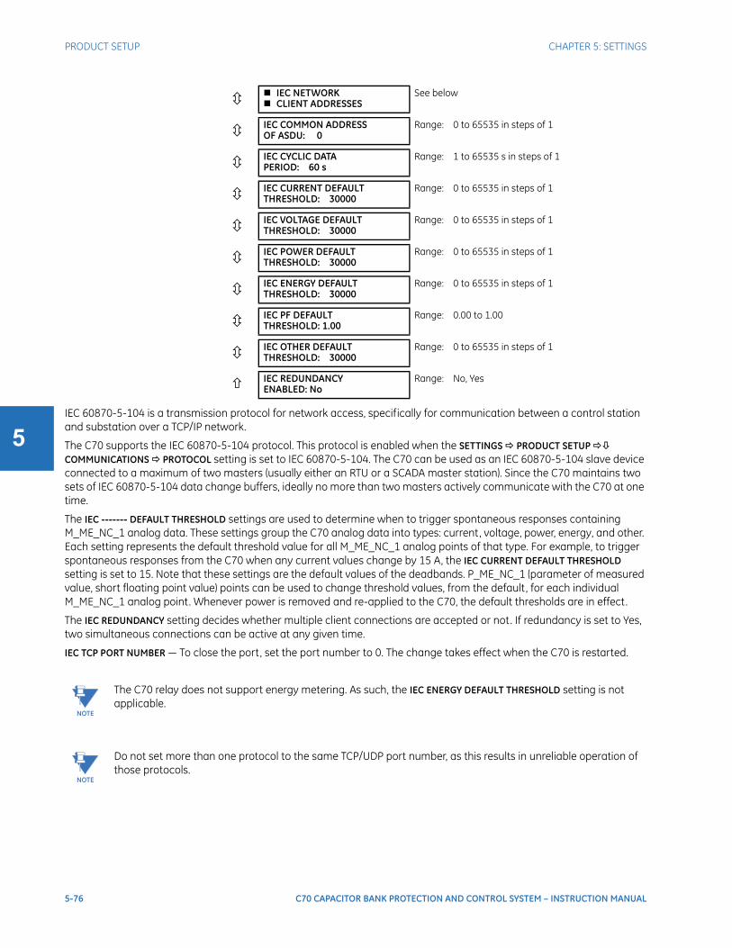
5-76 C70 CAPACITOR BANK PROTECTION AND CONTROL SYSTEM – INSTRUCTION MANUAL
PRODUCT SETUP CHAPTER 5: SETTINGS
5IEC 60870-5-104 is a transmission protocol for network access, specifically for communication between a control station and substation over a TCP/IP network.
The C70 supports the IEC 60870-5-104 protocol. This protocol is enabled when the SETTINGS PRODUCT SETUP COMMUNICATIONS PROTOCOL setting is set to IEC 60870-5-104. The C70 can be used as an IEC 60870-5-104 slave device connected to a maximum of two masters (usually either an RTU or a SCADA master station). Since the C70 maintains two sets of IEC 60870-5-104 data change buffers, ideally no more than two masters actively communicate with the C70 at one time.
The IEC ------- DEFAULT THRESHOLD settings are used to determine when to trigger spontaneous responses containing M_ME_NC_1 analog data. These settings group the C70 analog data into types: current, voltage, power, energy, and other. Each setting represents the default threshold value for all M_ME_NC_1 analog points of that type. For example, to trigger spontaneous responses from the C70 when any current values change by 15 A, the IEC CURRENT DEFAULT THRESHOLD setting is set to 15. Note that these settings are the default values of the deadbands. P_ME_NC_1 (parameter of measured value, short floating point value) points can be used to change threshold values, from the default, for each individual M_ME_NC_1 analog point. Whenever power is removed and re-applied to the C70, the default thresholds are in effect.
The IEC REDUNDANCY setting decides whether multiple client connections are accepted or not. If redundancy is set to Yes, two simultaneous connections can be active at any given time.
IEC TCP PORT NUMBER — To close the port, set the port number to 0. The change takes effect when the C70 is restarted.
IEC NETWORK CLIENT ADDRESSES
See below
IEC COMMON ADDRESSOF ASDU: 0
Range: 0 to 65535 in steps of 1
IEC CYCLIC DATAPERIOD: 60 s
Range: 1 to 65535 s in steps of 1
IEC CURRENT DEFAULTTHRESHOLD: 30000
Range: 0 to 65535 in steps of 1
IEC VOLTAGE DEFAULTTHRESHOLD: 30000
Range: 0 to 65535 in steps of 1
IEC POWER DEFAULTTHRESHOLD: 30000
Range: 0 to 65535 in steps of 1
IEC ENERGY DEFAULTTHRESHOLD: 30000
Range: 0 to 65535 in steps of 1
IEC PF DEFAULTTHRESHOLD: 1.00
Range: 0.00 to 1.00
IEC OTHER DEFAULTTHRESHOLD: 30000
Range: 0 to 65535 in steps of 1
IEC REDUNDANCYENABLED: No
Range: No, Yes
NOTE
The C70 relay does not support energy metering. As such, the IEC ENERGY DEFAULT THRESHOLD setting is not applicable.
NOTE
Do not set more than one protocol to the same TCP/UDP port number, as this results in unreliable operation of those protocols.

CHAPTER 5: SETTINGS PRODUCT SETUP
C70 CAPACITOR BANK PROTECTION AND CONTROL SYSTEM – INSTRUCTION MANUAL 5-77
5
SETTINGS PRODUCT SETUP COMMUNICATIONS IEC 60870-5-104 PROTOCOL IEC NETWORK CLIENT ADDRESSES
The C70 can specify a maximum of five clients for its IEC 104 connections. These are IP addresses for the controllers to which the C70 can connect. A maximum of two simultaneous connections are supported at any given time.
5.3.4.16 IEC 60870-5-103 protocolSETTINGS PRODUCT SETUP COMMUNICATIONS IEC 60870-5-103
IEC 60870-5-103 is a companion standard to the IEC 60870-5 suite of standards for transmission protocols. It defines messages and procedures for interoperability between protection equipment and devices of a control system in a substation for communicating on a serial line.
The IEC 60870-5-103 protocol is enabled when the SETTINGS PRODUCT SETUP COMMUNICATIONS PROTOCOL setting is set to IEC 60870-5-103.
The IEC 60870-5-103 is an unbalanced (master-slave) protocol for coded-bit serial communication, exchanging information with a control system. In the context of this protocol, the protection equipment is the slave and the control system is the master. The communication is based on a point-to-point principle. The master must be able to interpret the IEC 60870-5-103 communication messages.
The UR implementation of IEC 60870-5-103 consists of the following functions:
• Report binary inputs
• Report analog values (measurands)
• Commands
• Time synchronization
The RS485 port supports IEC 60870-5-103.
The UR Series Communications Guide contains more information on the protocol.
IEC103 COMMON ADDRESS OF ASDU — This setting uniquely defines this C70 on the serial line. Select an ID between 0 and 254. This ID does not need to be in sequential order for all stations that communicate with a controller, but it is recommended. Note that RS485 only allows a maximum of 32 slave stations on a communication line, so the entire range of 254 addresses is never exhausted.
IEC NETWORK CLIENT ADDRESSES CLIENT ADDRESS 1:
0.0.0.0Range: standard IPV4 address format
CLIENT ADDRESS 5:0.0.0.0
Range: standard IPV4 address format
IEC103 PROTOCOL IEC103 COMMON
ADDRESS OF ASDU: 0Range: 0 to 254 in steps of 1
IEC103 SYNC TIMEOUT:1
Range: 1 to 1440 min in steps of 1
IEC103 INPUTS BINARY
See below
IEC103 INPUTS MEASURANDS
See below
IEC103 COMMANDS
See below
The C70 is provided with optional IEC 60870-5-103 communications capability. This feature is specified as a software option at the time of ordering. See the Order Codes section in chapter 2 for details.
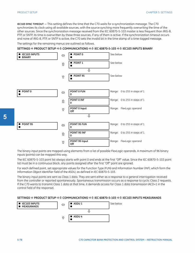
5-78 C70 CAPACITOR BANK PROTECTION AND CONTROL SYSTEM – INSTRUCTION MANUAL
PRODUCT SETUP CHAPTER 5: SETTINGS
5
IEC103 SYNC TIMEOUT — This setting defines the time that the C70 waits for a synchronization message. The C70 synchronizes its clock using all available sources, with the source synching more frequently overwriting the time of the other sources. Since the synchronization message received from the IEC 60870-5-103 master is less frequent than IRIG-B, PTP, or SNTP, its time is overwritten by these three sources, if any of them is active. If the synchronization timeout occurs and none of IRIG-B, PTP, or SNTP is active, the C70 sets the invalid bit in the time stamp of a time-tagged message.
The settings for the remaining menus are outlined as follows.
SETTINGS PRODUCT SETUP COMMUNICATIONS IEC 60870-5-103 IEC103 INPUTS BINARY
The binary input points are mapped using elements from a list of possible FlexLogic operands. A maximum of 96 binary inputs (points) can be mapped this way.
The IEC 60870-5-103 point list always starts with point 0 and ends at the first "Off" value. Since the IEC 60870-5-103 point list must be in a continuous block, any points assigned after the first "Off" point are ignored.
For each defined point, set appropriate values for the Function Type (FUN) and Information Number (INF), which form the Information Object Identifier field of the ASDU, as defined in IEC 60870-5-103.
The binary input points are sent as Class 1 data. They are sent either as a response to a general interrogation received from the controller or reported spontaneously. Spontaneous transmission occurs as a response to cyclic Class 2 requests. If the C70 wants to transmit Class 1 data at that time, it demands access for Class 1 data transmission (ACD=1 in the control field of the response).
SETTINGS PRODUCT SETUP COMMUNICATIONS IEC 60870-5-103 IEC103 INPUTS MEASURANDS
IEC103 INPUTS BINARY POINT 0
See below
POINT 1
See below
POINT 95
See below
POINT 0 POINT 0 FUN
0Range: 0 to 255 in steps of 1
POINT 0 INF0
Range: 0 to 255 in steps of 1
POINT 0 InputOff
Range: FlexLogic operand
POINT 95 POINT 95 FUN
0Range: 0 to 255 in steps of 1
POINT 95 INF0
Range: 0 to 255 in steps of 1
POINT 95 InputOff
Range: FlexLogic operand
IEC103 INPUTS MEASURANDS ASDU 1
See below
ASDU 4
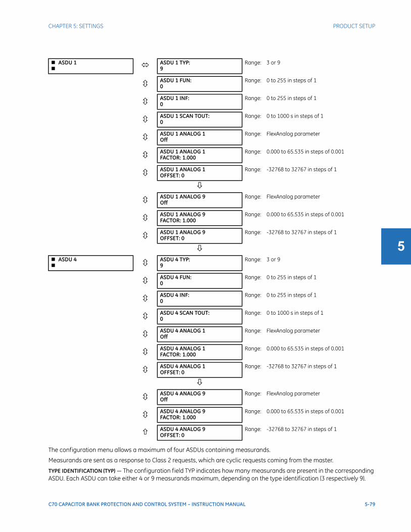
CHAPTER 5: SETTINGS PRODUCT SETUP
C70 CAPACITOR BANK PROTECTION AND CONTROL SYSTEM – INSTRUCTION MANUAL 5-79
5
The configuration menu allows a maximum of four ASDUs containing measurands.
Measurands are sent as a response to Class 2 requests, which are cyclic requests coming from the master.
TYPE IDENTIFICATION (TYP) — The configuration field TYP indicates how many measurands are present in the corresponding ASDU. Each ASDU can take either 4 or 9 measurands maximum, depending on the type identification (3 respectively 9).
ASDU 1 ASDU 1 TYP:
9Range: 3 or 9
ASDU 1 FUN:0
Range: 0 to 255 in steps of 1
ASDU 1 INF:0
Range: 0 to 255 in steps of 1
ASDU 1 SCAN TOUT:0
Range: 0 to 1000 s in steps of 1
ASDU 1 ANALOG 1Off
Range: FlexAnalog parameter
ASDU 1 ANALOG 1FACTOR: 1.000
Range: 0.000 to 65.535 in steps of 0.001
ASDU 1 ANALOG 1OFFSET: 0
Range: -32768 to 32767 in steps of 1
ASDU 1 ANALOG 9Off
Range: FlexAnalog parameter
ASDU 1 ANALOG 9 FACTOR: 1.000
Range: 0.000 to 65.535 in steps of 0.001
ASDU 1 ANALOG 9 OFFSET: 0
Range: -32768 to 32767 in steps of 1
ASDU 4 ASDU 4 TYP:
9Range: 3 or 9
ASDU 4 FUN:0
Range: 0 to 255 in steps of 1
ASDU 4 INF:0
Range: 0 to 255 in steps of 1
ASDU 4 SCAN TOUT:0
Range: 0 to 1000 s in steps of 1
ASDU 4 ANALOG 1Off
Range: FlexAnalog parameter
ASDU 4 ANALOG 1FACTOR: 1.000
Range: 0.000 to 65.535 in steps of 0.001
ASDU 4 ANALOG 1OFFSET: 0
Range: -32768 to 32767 in steps of 1
ASDU 4 ANALOG 9Off
Range: FlexAnalog parameter
ASDU 4 ANALOG 9 FACTOR: 1.000
Range: 0.000 to 65.535 in steps of 0.001
ASDU 4 ANALOG 9 OFFSET: 0
Range: -32768 to 32767 in steps of 1

5-80 C70 CAPACITOR BANK PROTECTION AND CONTROL SYSTEM – INSTRUCTION MANUAL
PRODUCT SETUP CHAPTER 5: SETTINGS
5
FUNCTION TYPE (FUN) and INFORMATION NUMBER (INF) — These two fields form the Information Object Identifier of the ASDU as defined in IEC 60870-103.
SCAN TIMEOUT (SCAN TOUT) — This is the cyclic period used by the C70 to decide when a measurand ASDU is included in a response. The measurand is sent as response to a Class 2 request when the corresponding timeout expires. The default value 0 means 500 ms.
ANALOG # — This field contains the actual measurand to be sent in the response to the master. The measurands can be mapped using elements from a list of FlexAnalog operands. The measurands sent are voltage, current, power, power factor, and frequency. If any other FlexAnalog is chosen, the C70 sends 0 instead of its value. Note that the power is transmitted in KW, not W. Measurands are transmitted as ASDU 3 or ASDU 9 (type identification value set to measurands I, respectively measurands II).
Each IEC 60870-5-103 measurands list ends at the first unconfigured ("Off") value. Any measurand assigned after the first "Off" value is ignored.
At least one measurand per ASDU must be configured in order to configure the following ASDU. For example, the user can configure only one measurand for each ASDU, but the user is not allowed to skip ASDU 2 and configure measurands in ASDU 3.
ANALOG # FACTOR and OFFSET — For each measurand included in the ASDU, a factor and offset also can be configured. The factor and offset allow for scaling to be performed on measurands. The final measurement sent to the IEC 60870-103 master is then "a*x + b," where x is the measurand, a is the multiplying factor and b is the offset. The master has to perform the reversed operation in order to retrieve the actual value if such scaling is done. By default a = 1 and b = 0, so no scaling is done if these values are left at their defaults. Examples of when scaling is appropriate are as follows:
• If the measured value contains decimals and it is important to preserve the resolution. Since the format for transmitting the measurand does not permit decimals, a factor a>1 can be applied before transmission. For example, a frequency F=59.9Hz can be transmitted as Ft = 10 * F = 10 * 59.9 = 599. In this case a = 10, b = 0. The master receives 599 and has to divide by 10 to retrieve the real value 59.9.
• If the measured value is larger than what fits in the format defined in IEC 103. The format defined in the standard allows for signed integers up to 4095. By offsetting, unsigned integers up to 4096 + 4095 = 8191 are supported. Scaling using factors <1 can be required in such cases. The calculation is outlined in the IEC 60870-5-103 chapter of the UR Series Communications Guide. Two examples follow, where you decide factors a and b.
Example 1: Nominal power Pn = 100 MW = 100000 KW (power is transmitted in KW)
Since P can be both positive and negative:
Transmitted power Pt = (4095/(Pn*2.4)) * P = (4095/(100000 * 2.4) ) * P
= 0.017 * P
a = 0.017
b = 0
Pt = 0.017 * P
For a max power 100000 KW * 2.4 = 240000 KW, we transmit
Pt = 0.017 * 240000 = 4080
A value above 240 MW is indicated by overflow.
Example 2: Nominal voltage Vn = 500000 V
Since RMS voltage V can be only positive:
Transmitted voltage Vt = (8191/(Vn*2.4)) * V - 4096 =
= (8191/(500000 * 2.4) ) * V - 4096 = 0.0068 * V - 4096
a = 0.0068
Since the step is in increments of 0.001, we round it at:
a = 0.006
b = -4096
Vt = 0.006 * V - 4096
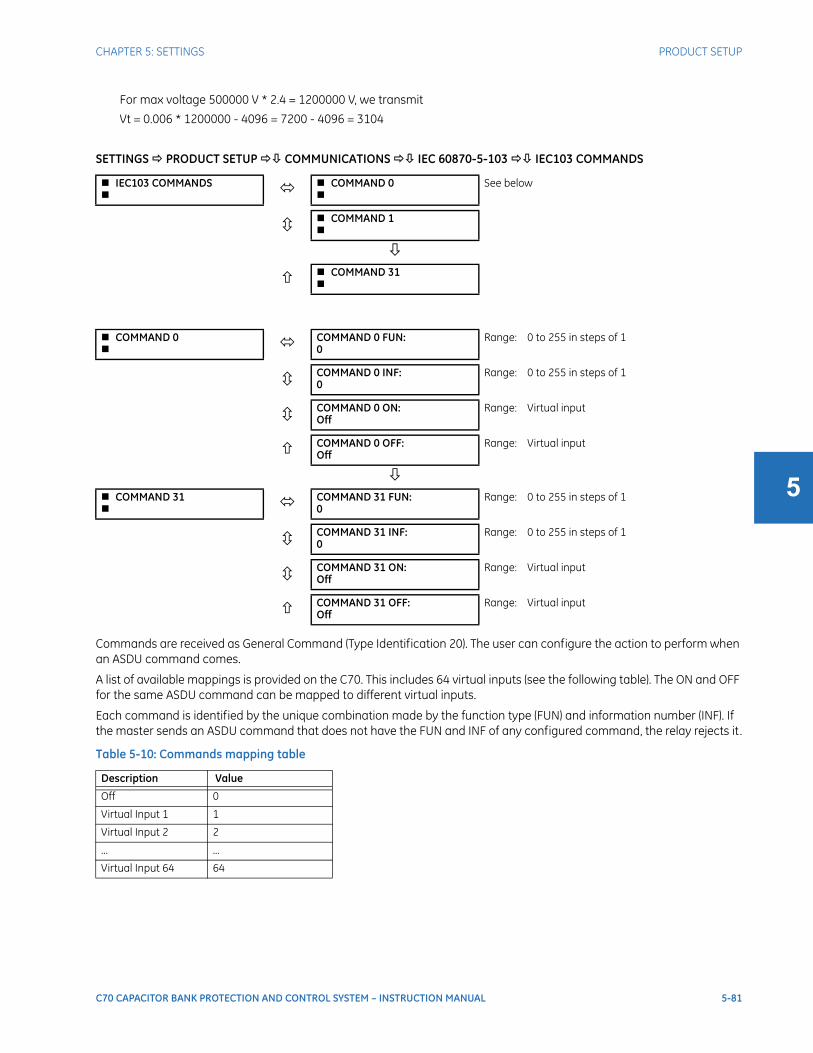
CHAPTER 5: SETTINGS PRODUCT SETUP
C70 CAPACITOR BANK PROTECTION AND CONTROL SYSTEM – INSTRUCTION MANUAL 5-81
5
For max voltage 500000 V * 2.4 = 1200000 V, we transmit
Vt = 0.006 * 1200000 - 4096 = 7200 - 4096 = 3104
SETTINGS PRODUCT SETUP COMMUNICATIONS IEC 60870-5-103 IEC103 COMMANDS
Commands are received as General Command (Type Identification 20). The user can configure the action to perform when an ASDU command comes.
A list of available mappings is provided on the C70. This includes 64 virtual inputs (see the following table). The ON and OFF for the same ASDU command can be mapped to different virtual inputs.
Each command is identified by the unique combination made by the function type (FUN) and information number (INF). If the master sends an ASDU command that does not have the FUN and INF of any configured command, the relay rejects it .
Table 5-10: Commands mapping table
IEC103 COMMANDS COMMAND 0
See below
COMMAND 1
COMMAND 31
COMMAND 0 COMMAND 0 FUN:
0Range: 0 to 255 in steps of 1
COMMAND 0 INF:0
Range: 0 to 255 in steps of 1
COMMAND 0 ON:Off
Range: Virtual input
COMMAND 0 OFF:Off
Range: Virtual input
COMMAND 31 COMMAND 31 FUN:
0Range: 0 to 255 in steps of 1
COMMAND 31 INF:0
Range: 0 to 255 in steps of 1
COMMAND 31 ON:Off
Range: Virtual input
COMMAND 31 OFF:Off
Range: Virtual input
Description Value
Off 0
Virtual Input 1 1
Virtual Input 2 2
... ...
Virtual Input 64 64

5-82 C70 CAPACITOR BANK PROTECTION AND CONTROL SYSTEM – INSTRUCTION MANUAL
PRODUCT SETUP CHAPTER 5: SETTINGS
5
5.3.5 Modbus user mapSETTINGS PRODUCT SETUP MODBUS USER MAP
The Modbus user map provides read-only access for up to 256 registers. To obtain a memory map value, enter the address in the ADDRESS line (converted from hex to decimal format). The corresponding value (if programmed) displays in the VALUE line. A value of “0” in subsequent register ADDRESS lines automatically returns values for the previous ADDRESS lines incremented by 1. An address value of “0” in the initial register means “none” and values of “0” display for all registers. Different ADDRESS values can be entered as required in any of the register positions.
The UR Series Communications Guide outlines the Modbus memory map. The map is also viewable in a web browser; enter the IP address of the C70 in a web browser and click the option.
5.3.6 Real-time clock
5.3.6.1 MenuSETTINGS PRODUCT SETUP REAL TIME CLOCK
The relay contains a real time clock (RTC) to create timestamps for communications protocols as well as for historical data, such as event records and oscillography. When the relay restarts, the RTC initializes from an onboard battery-backed clock, which has the same accuracy as an electronic watch, approximately ±1 minute per month (~23 ppm). Once the RTC is synchronized with the Precision Time Protocol (PTP), IRIG-B, or SNTP, its accuracy approaches that of the synchronizing time delivered to the relay.
The SYNCHRONIZING SOURCE setting configures the priority sequence of the time synchronization source, to determine which of the available external time sources to use for time synchronization. A setting of None causes the RTC and the synchrophasor clock to free-run. A setting of PP/IRIG-B/PTP/SNTP, IRIG-B/PP/PTP/SNTP, or PP/PTP/IRIG-B/SNTP causes the relay to track the first source named that is enabled and operational, or free-run if none of these are available. Here, PP means a time source that is strictly compliant with PP, and PTP means a time source that is not strictly compliant with PP. When a time source fails or recovers, the relay automatically transfers synchronization as required by this setting.
Setup for IRIG-B is illustrated in the Installation chapter.
The clock is updated by all sources active in the device. This means that whenever a time synchronization message is received through any of the active protocols, the C70 clock updates. However, given that IEC 60870-5-103, IEC 60870-5-104, Modbus, and DNP are low-accuracy time synchronization methods, avoid their use for synchronization when better accuracy time protocols, such as IRIG-B, PTP, and SNTP, are active in the system.
MODBUS USER MAP ADDRESS 1: 0
VALUE: 0Range: 0 to 65535 in steps of 1
ADDRESS 256: 0VALUE: 0
Range: 0 to 65535 in steps of 1
REAL TIME CLOCK SYNCRONIZING SOURCE:
NoneRange: None, PP/IRIG-B/PTP/SNTP, IRIG-B/PP/PTP/SNTP, PP/PTP/IRIG-B/SNTP
REAL TIME CLOCKEVENTS: Disabled
Range: Enabled, Disabled
IRIG-B SIGNAL TYPE:None
Range: None, DC Shift, Amplitude Modulated
PRECISION TIME PROTOCOL (1588)
See below
SNTP PROTOCOL
See below
LOCAL TIME
See below
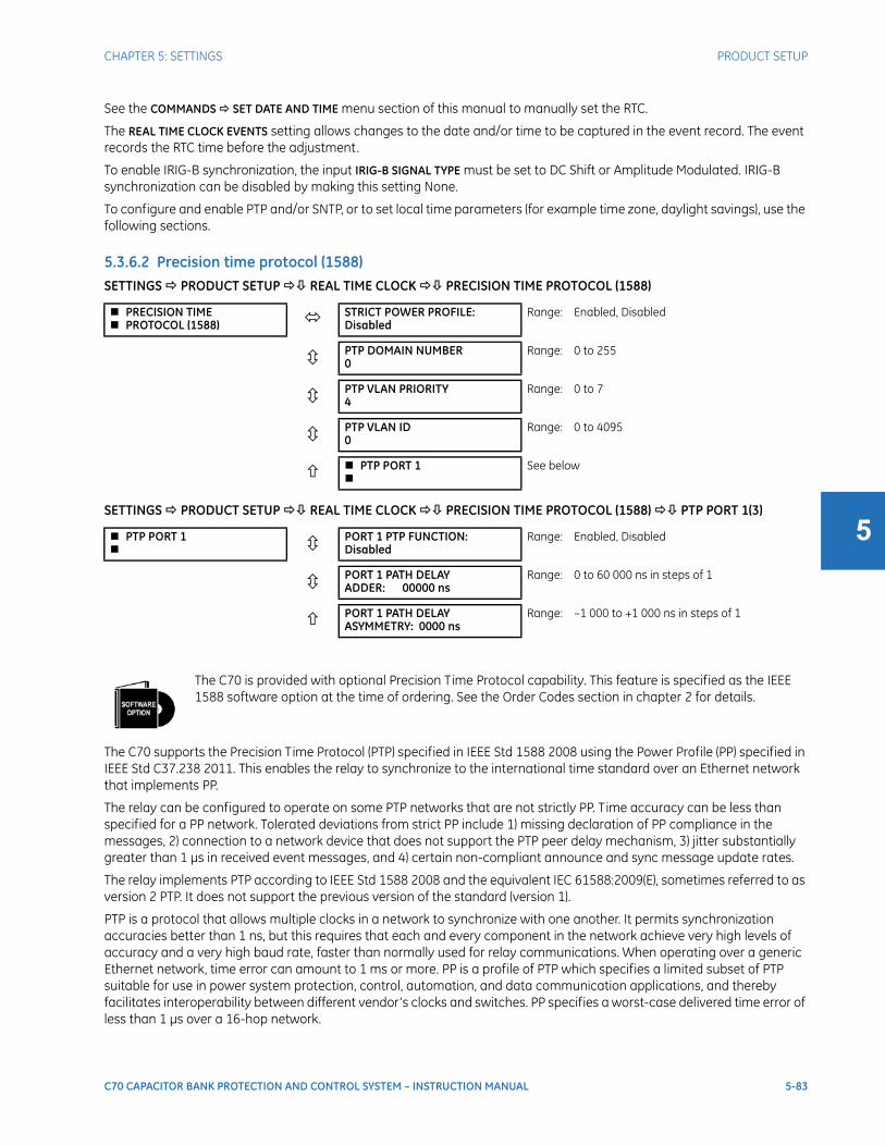
CHAPTER 5: SETTINGS PRODUCT SETUP
C70 CAPACITOR BANK PROTECTION AND CONTROL SYSTEM – INSTRUCTION MANUAL 5-83
5
See the COMMANDS SET DATE AND TIME menu section of this manual to manually set the RTC.
The REAL TIME CLOCK EVENTS setting allows changes to the date and/or time to be captured in the event record. The event records the RTC time before the adjustment.
To enable IRIG-B synchronization, the input IRIG-B SIGNAL TYPE must be set to DC Shift or Amplitude Modulated. IRIG-B synchronization can be disabled by making this setting None.
To configure and enable PTP and/or SNTP, or to set local time parameters (for example time zone, daylight savings), use the following sections.
5.3.6.2 Precision time protocol (1588)SETTINGS PRODUCT SETUP REAL TIME CLOCK PRECISION TIME PROTOCOL (1588)
SETTINGS PRODUCT SETUP REAL TIME CLOCK PRECISION TIME PROTOCOL (1588) PTP PORT 1(3)
The C70 supports the Precision Time Protocol (PTP) specified in IEEE Std 1588 2008 using the Power Profile (PP) specified in IEEE Std C37.238 2011. This enables the relay to synchronize to the international time standard over an Ethernet network that implements PP.
The relay can be configured to operate on some PTP networks that are not strictly PP. Time accuracy can be less than specified for a PP network. Tolerated deviations from strict PP include 1) missing declaration of PP compliance in the messages, 2) connection to a network device that does not support the PTP peer delay mechanism, 3) jitter substantially greater than 1 µs in received event messages, and 4) certain non-compliant announce and sync message update rates.
The relay implements PTP according to IEEE Std 1588 2008 and the equivalent IEC 61588:2009(E), sometimes referred to as version 2 PTP. It does not support the previous version of the standard (version 1).
PTP is a protocol that allows multiple clocks in a network to synchronize with one another. It permits synchronization accuracies better than 1 ns, but this requires that each and every component in the network achieve very high levels of accuracy and a very high baud rate, faster than normally used for relay communications. When operating over a generic Ethernet network, time error can amount to 1 ms or more. PP is a profile of PTP which specifies a limited subset of PTP suitable for use in power system protection, control, automation, and data communication applications, and thereby facilitates interoperability between different vendor’s clocks and switches. PP specifies a worst-case delivered time error of less than 1 µs over a 16-hop network.
PRECISION TIME PROTOCOL (1588) STRICT POWER PROFILE:
DisabledRange: Enabled, Disabled
PTP DOMAIN NUMBER0
Range: 0 to 255
PTP VLAN PRIORITY4
Range: 0 to 7
PTP VLAN ID0
Range: 0 to 4095
PTP PORT 1
See below
PTP PORT 1 PORT 1 PTP FUNCTION:
DisabledRange: Enabled, Disabled
PORT 1 PATH DELAYADDER: 00000 ns
Range: 0 to 60 000 ns in steps of 1
PORT 1 PATH DELAYASYMMETRY: 0000 ns
Range: –1 000 to +1 000 ns in steps of 1
The C70 is provided with optional Precision Time Protocol capability. This feature is specified as the IEEE 1588 software option at the time of ordering. See the Order Codes section in chapter 2 for details.

5-84 C70 CAPACITOR BANK PROTECTION AND CONTROL SYSTEM – INSTRUCTION MANUAL
PRODUCT SETUP CHAPTER 5: SETTINGS
5
In a PTP system and in a PP system, the clocks automatically organize themselves into a master-slave synchronization hierarchy with the “best” clock available making itself the "grandmaster" at the top of the hierarchy; all others make themselves “slaves” and track the grandmaster. Typically the grandmaster clock receives its time from GPS satellites or some other link to the international time standard. If the grandmaster fails, the next “best” clock available in the domain assumes the grandmaster role. When a clock on start-up discovers that it is “better” than the present grandmaster, it assumes the grandmaster role and the previous grandmaster reverts to slave.
Time messages issued by the grandmaster are delayed as they pass through the network both due to the finite speed of the signal in the interconnecting fiber or wire, and due to processing delays in the Ethernet switches. Each clock and switch implementing PP measures the propagation delay to each of its PP neighbors, and compensates for these delays in the time received. Each network device implementing PP measures the processing delay it introduces in each time message and compensates for this delay in the time it transmits. As a result, the time delivered to end-devices such as the UR are virtually identical to the grandmaster time. If one of the network devices in the hierarchy does not fully implement PP, the associated propagation delay and/or latency may not be compensated for, and the time received at the end-device can be in error by more than 100 µs.
See the preceding Real Time Clock section for a description of when time values received via PTP are used to update the relay’s real time clock.
The following settings are available for configuring the relay for PTP. The PTP menu displays only when the option was purchased.
STRICT POWER PROFILE — Power profile (IEEE Std C37.238 2011) requires that the relay only select a power profile compliant clock as a grandmaster, that the delivered time have worst-case error of ±1 µs, and that the peer delay mechanism be implemented. With the strict power profile setting enabled, the relay only selects as master the clocks displaying the IEEE_C37_238 identification codes. It uses a port only when the peer delay mechanism is operational. With the strict power profile setting disabled, the relay uses clocks without the power profile identification when no power profile clocks are present, and uses ports even if the peer delay mechanism is non-operational. This setting applies to all of the relay’s PTP capable ports.
PTP DOMAIN NUMBER — Set this setting to the domain number of the grandmaster-capable clock(s) to be synchronized to. A network can support multiple time distribution domains, each distinguished with a unique domain number. More commonly, there is a single domain using the default domain number zero.
This setting applies to all of the relay’s PTP capable ports.
PTP VLAN PRIORITY — This setting selects the value of the priority field in the 802.1Q VLAN tag in request messages issued by the relay’s peer delay mechanism. In compliance with PP the default VLAN priority is 4, but it is recommended that it be set to 7 in accordance with PTP. Depending on the characteristics of the device to which the relay is linked directly, VLAN Priority can have no effect.
This setting applies to all of the relay’s PTP capable ports.
PTP VLAN ID — This setting selects the value of the ID field in the 802.1Q VLAN tag in request messages issued by the relay’s peer delay mechanism. It is provided in compliance with PP. As these messages have a destination address that indicates they are not to be bridged, their VLAN ID serves no function, and so can be left at its default value. Depending on the characteristics of the device to which the relay is linked directly, VLAN ID can have no effect. This setting applies to all of the relay’s PTP capable ports.
PORT 1 ... 3 FUNCTION — While this port setting is selected to disabled, PTP is disabled on this port. The relay does not generate or listen to PTP messages on this port.
PORT 1 ... 3 PATH DELAY ADDER — The time delivered by PTP is advanced by the time value in this setting prior to the time being used to synchronize the relay’s real time clock. This is to compensate to the extent practical for time delivery delays not compensated for in the network. In a fully compliant PP network, the peer delay and the processing delay mechanisms compensate for all the delays between the grandmaster and the relay. In such networks, make this setting zero.
In networks containing one or more switches and/or clocks that do not implement both of these mechanisms, not all delays are compensated, so the time of message arrival at the relay is later than the time indicated in the message. This setting can be used to approximately compensate for this delay. However, as the relay is not aware of network switching that dynamically changes the amount of uncompensated delay, there is no setting that always and completely corrects for uncompensated delay. A setting can be chosen that reduces the worst-case error to half of the range between minimum and maximum uncompensated delay, if these values are known.

CHAPTER 5: SETTINGS PRODUCT SETUP
C70 CAPACITOR BANK PROTECTION AND CONTROL SYSTEM – INSTRUCTION MANUAL 5-85
5
PORT 1 ... 3 PATH DELAY ASSYMMETRY — This setting corresponds to “delayAsymmetry” in PTP, which is used by the peer delay mechanism to compensate for any difference in the propagation delay between the two directions of a link. Except in unusual cases, the two fibers are of essentially identical length and composition, so make this setting zero.
In unusual cases where the length of the link is different in different directions, set this setting to the number of nanoseconds the Ethernet propagation delay to the relay is longer than the mean of path propagation delays to and from the relay. For instance, if it is known say from the physical length of the fibers and the propagation speed in the fibers that the delay from the relay to the Ethernet switch it is connected to is 9000 ns and that the delay from the switch to the relay is 11000 ns, then the mean delay is 10000 ns, and the path delay asymmetry is 11000 - 10000 = +1000 ns.
5.3.6.3 SNTP protocolSETTINGS PRODUCT SETUP REAL TIME CLOCK SNTP PROTOCOL
The C70 supports the Simple Network Time Protocol specified in RFC-2030. With SNTP, the C70 can obtain clock time over an Ethernet network. The C70 acts as an SNTP client to receive time values from an SNTP/NTP server, usually a dedicated product using a GPS receiver. UR series relays support unicast, broadcast, multicast, and anycast SNTP functionality.
The SNTP FUNCTION setting enables or disables the SNTP feature on the C70.
To use SNTP in unicast mode, set SNTP SERVER IP ADDR to the SNTP/NTP server IP address. Once this address is set and SNTP FUNCTION is “Enabled,” the C70 attempts to obtain time values from the SNTP/NTP server. Since many time values are obtained and averaged, it generally takes three to four minutes until the C70 clock is closely synchronized with the SNTP/NTP server. It takes up to two minutes for the C70 to signal an SNTP self-test error if the server is offline.
To use SNTP in broadcast mode, set the SNTP SERVER IP ADDR setting to “0.0.0.0” and SNTP FUNCTION to “Enabled.” The C70 then listens to SNTP messages sent to the “all ones” broadcast address for the subnet. The C70 waits up to 18 minutes (>1024 seconds) without receiving an SNTP broadcast message before signaling an SNTP self-test error.
The SNTP UDP PORT NUMBER is 123 for normal SNTP operation. If SNTP is not required, close the port by setting the port number to 0, after which the change takes effect when the C70 is restarted.
5.3.6.4 Local timeSETTINGS PRODUCT SETUP REAL TIME CLOCK LOCAL TIME
SNTP PROTOCOL SNTP FUNCTION:
DisabledRange: Enabled, Disabled
SNTP SERVER IP ADDR:0.0.0.0
Range: standard IP address format
SNTP UDP PORTNUMBER: 123
Range: 0 to 65535 in steps of 1
NOTE
Do not set more than one protocol to the same TCP/UDP port number, as this results in unreliable operation of those protocols.
LOCAL TIME LOCAL TIME OFFSET
FROM UTC: 0.0 hrRange: –24.0 to 24.0 hr in steps of 0.5
DAYLIGHT SAVINGSTIME: Disabled
Range: Disabled, Enabled
DST START MONTH:January
Range: January to December (all months)
DST START DAY:Sunday
Range: Sunday to Saturday (all days of the week)
DST START DAYINSTANCE: First
Range: First, Second, Third, Fourth, Last
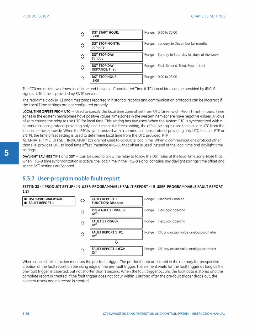
5-86 C70 CAPACITOR BANK PROTECTION AND CONTROL SYSTEM – INSTRUCTION MANUAL
PRODUCT SETUP CHAPTER 5: SETTINGS
5
The C70 maintains two times: local time and Universal Coordinated Time (UTC). Local time can be provided by IRIG-B signals. UTC time is provided by SNTP servers.
The real-time clock (RTC) and timestamps reported in historical records and communication protocols can be incorrect if the Local Time settings are not configured properly.
LOCAL TIME OFFSET FROM UTC — Used to specify the local time zone offset from UTC (Greenwich Mean Time) in hours. Time zones in the eastern hemisphere have positive values; time zones in the western hemisphere have negative values. A value of zero causes the relay to use UTC for local time. This setting has two uses. When the system RTC is synchronized with a communications protocol providing only local time or it is free-running, the offset setting is used to calculate UTC from the local time these provide. When the RTC is synchronized with a communications protocol providing only UTC (such as PTP or SNTP), the time offset setting is used to determine local time from the UTC provided. PTP ALTERNATE_TIME_OFFSET_INDICATOR TLVs are not used to calculate local time. When a communications protocol other than PTP provides UTC to local time offset (meaning IRIG-B), that offset is used instead of the local time and daylight time settings.
DAYLIGHT SAVINGS TIME and DST — Can be used to allow the relay to follow the DST rules of the local time zone. Note that when IRIG-B time synchronization is active, the local time in the IRIG-B signal contains any daylight savings time offset and so the DST settings are ignored.
5.3.7 User-programmable fault reportSETTINGS PRODUCT SETUP USER-PROGRAMMABLE FAULT REPORT USER-PROGRAMMABLE FAULT REPORT 1(2)
When enabled, this function monitors the pre-fault trigger. The pre-fault data are stored in the memory for prospective creation of the fault report on the rising edge of the pre-fault trigger. The element waits for the fault trigger as long as the pre-fault trigger is asserted, but not shorter than 1 second. When the fault trigger occurs, the fault data is stored and the complete report is created. If the fault trigger does not occur within 1 second after the pre-fault trigger drops out, the element resets and no record is created.
DST START HOUR:2:00
Range: 0:00 to 23:00
DST STOP MONTH:January
Range: January to December (all months)
DST STOP DAY:Sunday
Range: Sunday to Saturday (all days of the week)
DST STOP DAYINSTANCE: First
Range: First, Second, Third, Fourth, Last
DST STOP HOUR:2:00
Range: 0:00 to 23:00
USER-PROGRAMMABLE FAULT REPORT 1 FAULT REPORT 1
FUNCTION: DisabledRange: Disabled, Enabled
PRE-FAULT 1 TRIGGER:Off
Range: FlexLogic operand
FAULT 1 TRIGGER:Off
Range: FlexLogic operand
FAULT REPORT 1 #1:Off
Range: Off, any actual value analog parameter
FAULT REPORT 1 #32:Off
Range: Off, any actual value analog parameter
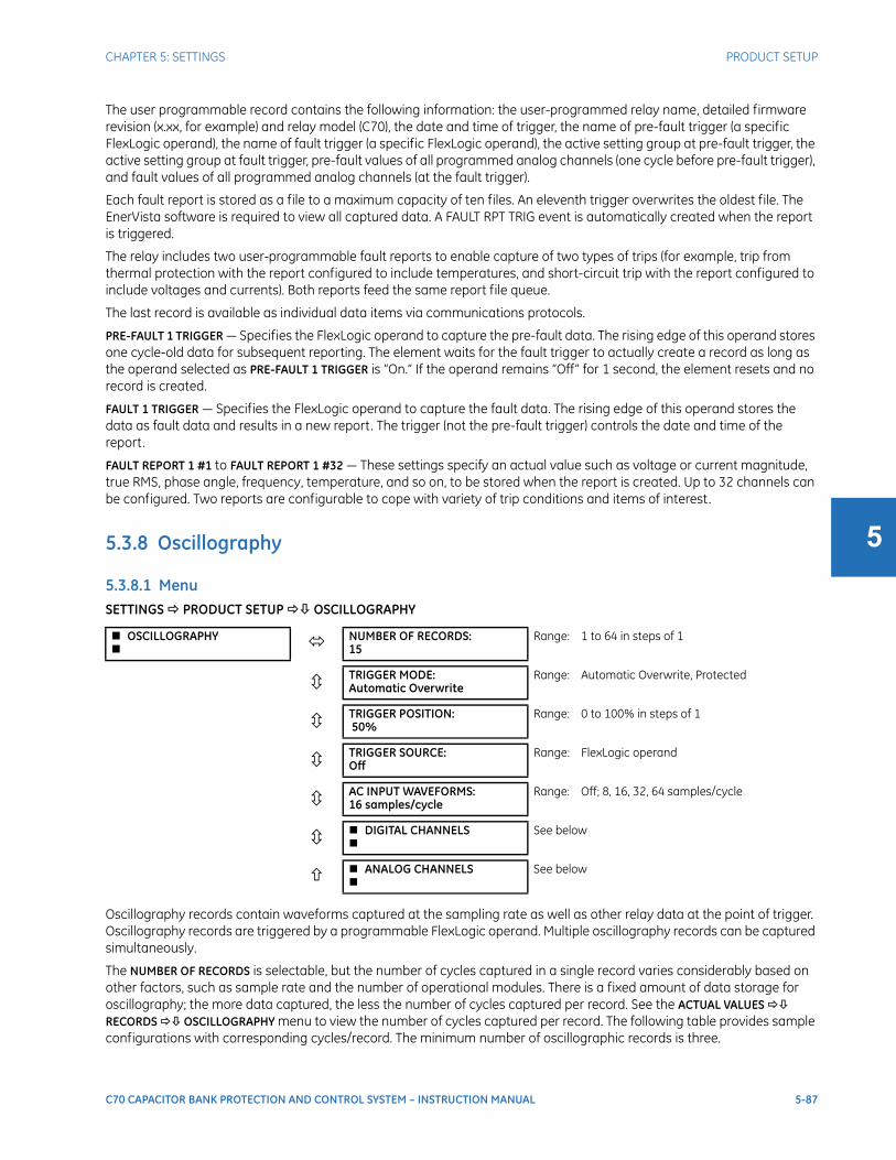
CHAPTER 5: SETTINGS PRODUCT SETUP
C70 CAPACITOR BANK PROTECTION AND CONTROL SYSTEM – INSTRUCTION MANUAL 5-87
5
The user programmable record contains the following information: the user-programmed relay name, detailed firmware revision (x.xx, for example) and relay model (C70), the date and time of trigger, the name of pre-fault trigger (a specific FlexLogic operand), the name of fault trigger (a specific FlexLogic operand), the active setting group at pre-fault trigger, the active setting group at fault trigger, pre-fault values of all programmed analog channels (one cycle before pre-fault trigger), and fault values of all programmed analog channels (at the fault trigger).
Each fault report is stored as a file to a maximum capacity of ten files. An eleventh trigger overwrites the oldest file. The EnerVista software is required to view all captured data. A FAULT RPT TRIG event is automatically created when the report is triggered.
The relay includes two user-programmable fault reports to enable capture of two types of trips (for example, trip from thermal protection with the report configured to include temperatures, and short-circuit trip with the report configured to include voltages and currents). Both reports feed the same report file queue.
The last record is available as individual data items via communications protocols.
PRE-FAULT 1 TRIGGER — Specifies the FlexLogic operand to capture the pre-fault data. The rising edge of this operand stores one cycle-old data for subsequent reporting. The element waits for the fault trigger to actually create a record as long as the operand selected as PRE-FAULT 1 TRIGGER is “On.” If the operand remains “Off” for 1 second, the element resets and no record is created.
FAULT 1 TRIGGER — Specifies the FlexLogic operand to capture the fault data. The rising edge of this operand stores the data as fault data and results in a new report. The trigger (not the pre-fault trigger) controls the date and time of the report.
FAULT REPORT 1 #1 to FAULT REPORT 1 #32 — These settings specify an actual value such as voltage or current magnitude, true RMS, phase angle, frequency, temperature, and so on, to be stored when the report is created. Up to 32 channels can be configured. Two reports are configurable to cope with variety of trip conditions and items of interest.
5.3.8 Oscillography
5.3.8.1 MenuSETTINGS PRODUCT SETUP OSCILLOGRAPHY
Oscillography records contain waveforms captured at the sampling rate as well as other relay data at the point of trigger. Oscillography records are triggered by a programmable FlexLogic operand. Multiple oscillography records can be captured simultaneously.
The NUMBER OF RECORDS is selectable, but the number of cycles captured in a single record varies considerably based on other factors, such as sample rate and the number of operational modules. There is a fixed amount of data storage for oscillography; the more data captured, the less the number of cycles captured per record. See the ACTUAL VALUES RECORDS OSCILLOGRAPHY menu to view the number of cycles captured per record. The following table provides sample configurations with corresponding cycles/record. The minimum number of oscillographic records is three.
OSCILLOGRAPHY NUMBER OF RECORDS:
15Range: 1 to 64 in steps of 1
TRIGGER MODE:Automatic Overwrite
Range: Automatic Overwrite, Protected
TRIGGER POSITION:50%
Range: 0 to 100% in steps of 1
TRIGGER SOURCE:Off
Range: FlexLogic operand
AC INPUT WAVEFORMS:16 samples/cycle
Range: Off; 8, 16, 32, 64 samples/cycle
DIGITAL CHANNELS
See below
ANALOG CHANNELS
See below

5-88 C70 CAPACITOR BANK PROTECTION AND CONTROL SYSTEM – INSTRUCTION MANUAL
PRODUCT SETUP CHAPTER 5: SETTINGS
5
Table 5-11: Oscillography cycles/record example
TRIGGER MODE — A new record automatically overwrites an older record when TRIGGER MODE is set to “Automatic Overwrite.”
TRIGGER POSITION — Set this to a percentage of the total buffer size (for example, 10%, 50%, 75%, and so on). A trigger position of 25% consists of 25% pre- and 75% post-trigger data.
TRIGGER SOURCE — Always captured in oscillography and can be any FlexLogic parameter (element state, contact input, virtual output, and so on). The relay sampling rate is 64 samples per cycle.
AC INPUT WAVEFORMS — Determines the sampling rate at which AC input signals (that is, current and voltage) are stored. Reducing the sampling rate allows longer records to be stored. This setting has no effect on the internal sampling rate of the relay, which is always 64 samples per cycle. That is, it has no effect on the fundamental calculations of the device.
5.3.8.2 Digital channelsSETTINGS PRODUCT SETUP OSCILLOGRAPHY DIGITAL CHANNELS
DIGITAL 1(63) CHANNEL — This setting selects the FlexLogic operand state recorded in an oscillography trace. The length of each oscillography trace depends in part on the number of parameters selected here. Parameters set to “Off” are ignored.
5.3.8.3 Analog channelsSETTINGS PRODUCT SETUP OSCILLOGRAPHY ANALOG CHANNELS
These settings select the metering actual value recorded in an oscillography trace. The length of each oscillography trace depends in part on the number of parameters selected here. Parameters set to “Off” are ignored. The parameters available in a given relay depend on
• the type of relay,
Records CT/VTs Sample rate Digital Analog Cycles/record
3 1 8 0 0 14663
3 1 16 16 0 6945
8 1 16 16 0 3472
8 1 16 16 4 2868
8 2 16 16 4 1691
8 2 16 63 16 1221
8 2 32 63 16 749
8 2 64 63 16 422
32 2 64 63 16 124
NOTE
When changes are made to the oscillography settings, all existing oscillography records are cleared.
DIGITAL CHANNELS DIGITAL CHANNEL 1:
OffRange: FlexLogic operand
DIGITAL CHANNEL 63:Off
Range: FlexLogic operand
ANALOG CHANNELS ANALOG CHANNEL 1:
OffRange: Off, any FlexAnalog parameterSee Appendix A for list
ANALOG CHANNEL 16:Off
Range: Off, any FlexAnalog parameterSee Appendix A for list
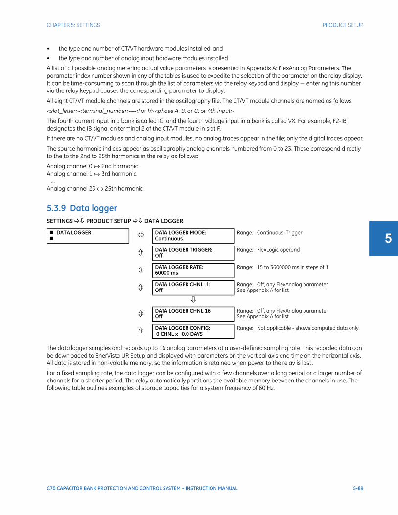
CHAPTER 5: SETTINGS PRODUCT SETUP
C70 CAPACITOR BANK PROTECTION AND CONTROL SYSTEM – INSTRUCTION MANUAL 5-89
5
• the type and number of CT/VT hardware modules installed, and
• the type and number of analog input hardware modules installed
A list of all possible analog metering actual value parameters is presented in Appendix A: FlexAnalog Parameters. The parameter index number shown in any of the tables is used to expedite the selection of the parameter on the relay display. It can be time-consuming to scan through the list of parameters via the relay keypad and display — entering this number via the relay keypad causes the corresponding parameter to display.
All eight CT/VT module channels are stored in the oscillography file. The CT/VT module channels are named as follows:
<slot_letter><terminal_number>—<I or V><phase A, B, or C, or 4th input>
The fourth current input in a bank is called IG, and the fourth voltage input in a bank is called VX. For example, F2-IB designates the IB signal on terminal 2 of the CT/VT module in slot F.
If there are no CT/VT modules and analog input modules, no analog traces appear in the file; only the digital traces appear.
The source harmonic indices appear as oscillography analog channels numbered from 0 to 23. These correspond directly to the to the 2nd to 25th harmonics in the relay as follows:
Analog channel 0 ↔ 2nd harmonicAnalog channel 1 ↔ 3rd harmonic
...Analog channel 23 ↔ 25th harmonic
5.3.9 Data loggerSETTINGS PRODUCT SETUP DATA LOGGER
The data logger samples and records up to 16 analog parameters at a user-defined sampling rate. This recorded data can be downloaded to EnerVista UR Setup and displayed with parameters on the vertical axis and time on the horizontal axis. All data is stored in non-volatile memory, so the information is retained when power to the relay is lost.
For a fixed sampling rate, the data logger can be configured with a few channels over a long period or a larger number of channels for a shorter period. The relay automatically partitions the available memory between the channels in use. The following table outlines examples of storage capacities for a system frequency of 60 Hz.
DATA LOGGER DATA LOGGER MODE:
ContinuousRange: Continuous, Trigger
DATA LOGGER TRIGGER:Off
Range: FlexLogic operand
DATA LOGGER RATE:60000 ms
Range: 15 to 3600000 ms in steps of 1
DATA LOGGER CHNL 1:Off
Range: Off, any FlexAnalog parameterSee Appendix A for list
DATA LOGGER CHNL 16:Off
Range: Off, any FlexAnalog parameterSee Appendix A for list
DATA LOGGER CONFIG:0 CHNL x 0.0 DAYS
Range: Not applicable - shows computed data only
5-90 C70 CAPACITOR BANK PROTECTION AND CONTROL SYSTEM – INSTRUCTION MANUAL
PRODUCT SETUP CHAPTER 5: SETTINGS
5
Table 5-12: Data logger storage capacity example
DATA LOGGER MODE — This setting configures the mode in which the data logger operates. When set to “Continuous,” the data logger actively records any configured channels at the rate as defined by the DATA LOGGER RATE. The data logger is idle in this mode when no channels are configured. When set to “Trigger,” the data logger records any configured channels at the instance of the rising edge of the DATA LOGGER TRIGGER source FlexLogic operand. The data logger ignores all subsequent triggers and continues to record data until the active record is full. Once the data logger is full, a CLEAR DATA LOGGER command is required to clear the data logger record before a new record can be started. Performing the CLEAR DATA LOGGER command also stops the current record and resets the data logger to be ready for the next trigger.
DATA LOGGER TRIGGER — This setting selects the signal used to trigger the start of a new data logger record. Any FlexLogic operand can be used as the trigger source. This setting only applies when the mode is set to “Trigger.”
DATA LOGGER RATE — This setting selects the time interval at which the actual value data is recorded.
DATA LOGGER CHNL 1(16) — This setting selects the metering actual value that is to be recorded in Channel 1(16) of the data log. The parameters available in a given relay are dependent on: the type of relay, the type and number of CT/VT hardware modules installed, and the type and number of Analog Input hardware modules installed. Upon startup, the relay automatically prepares the parameter list. A list of all possible analog metering actual value parameters is shown in Appendix A: FlexAnalog Parameters. The parameter index number shown in any of the tables is used to expedite the selection of the parameter on the relay display. It can be time-consuming to scan through the list of parameters via the relay keypad/display—entering this number via the relay keypad causes the corresponding parameter to display.
DATA LOGGER CONFIG — This display presents the total amount of time that the Data Logger can record the channels not selected to “Off” without overwriting old data.
5.3.10 User-programmable LEDs
5.3.10.1 MenuSETTINGS PRODUCT SETUP USER-PROGRAMMABLE LEDS
Sampling rate Channels Days Storage capacity
15 ms 1 0.1 954 s
8 0.1 120 s
9 0.1 107 s
16 0.1 60 s
1000 ms 1 0.7 65457 s
8 0.1 8182 s
9 0.1 7273 s
16 0.1 4091 s
60000 ms 1 45.4 3927420 s
8 5.6 490920 s
9 5 436380 s
16 2.8 254460 s
3600000 ms 1 2727.5 235645200 s
8 340.9 29455200 s
9 303 26182800 s
NOTE
Changing any setting affecting data logger operation clears data in the log.
USER-PROGRAMMABLE LEDS LED TEST
See below

CHAPTER 5: SETTINGS PRODUCT SETUP
C70 CAPACITOR BANK PROTECTION AND CONTROL SYSTEM – INSTRUCTION MANUAL 5-91
5
The 48 amber LEDs on relay panels 2 and 3 can be customized to illuminate when a selected FlexLogic operand is in the logic 1 state. The trip and alarm LEDs on panel 1 can also be customized in a similar manner. To ensure correct functionality of all LEDs, an LED test feature is also provided.
5.3.10.2 LED testSETTINGS PRODUCT SETUP USER-PROGRAMMABLE LEDS LED TEST
When enabled, the LED test can be initiated from any digital input or user-programmable condition, such as a user-programmable pushbutton. The control operand is configured under the LED TEST CONTROL setting. The test covers all LEDs, including the LEDs of the optional user-programmable pushbuttons.
The test consists of the following three stages:
1. All 62 LEDs on the relay are illuminated. This is a quick test to verify if any of the LEDs is “burned.” This stage lasts as long as the control input is on, up to a maximum of 1 minute. After 1 minute, the test ends.
2. All the LEDs are turned off, and then one LED at a time turns on for 1 second, then back off. The test routine starts at the top left panel, moving from the top to bottom of each LED column. This test checks for hardware failures that lead to more than one LED being turned on from a single logic point. This stage can be interrupted at any time.
3. All the LEDs are turned on. One LED at a time turns off for 1 second, then back on. The test routine starts at the top left panel moving from top to bottom of each column of the LEDs. This test checks for hardware failures that lead to more than one LED being turned off from a single logic point. This stage can be interrupted at any time.
When testing is in progress, the LEDs are controlled by the test sequence, rather than the protection, control, and monitoring features. However, the LED control mechanism accepts all the changes to LED states generated by the relay and stores the actual LED states (on or off) in memory. When the test completes, the LEDs reflect the actual state resulting from relay response during testing. The reset pushbutton does not clear any targets when the LED Test is in progress.
A dedicated FlexLogic operand, LED TEST IN PROGRESS, is set for the duration of the test. When the test sequence is initiated, the LED TEST INITIATED event is stored in the event recorder.
The entire test procedure is user-controlled. In particular, stage 1 can last as long as necessary, and stages 2 and 3 can be interrupted. The test responds to the position and rising edges of the control input defined by the LED TEST CONTROL setting. The control pulses must last at least 250 ms to take effect. The following diagram explains how the test is executed.
TRIP & ALARM LEDS
See page 5-93
USER-PROGRAMMABLE LED 1
See page 5-93
USER-PROGRAMMABLE LED 48
LED TEST LED TEST FUNCTION:
DisabledRange: Disabled, Enabled
LED TEST CONTROL:Off
Range: FlexLogic operand

5-92 C70 CAPACITOR BANK PROTECTION AND CONTROL SYSTEM – INSTRUCTION MANUAL
PRODUCT SETUP CHAPTER 5: SETTINGS
5
Figure 5-32: LED test sequence
Application example 1Assume one needs to check if any of the LEDs is “burned” through user-programmable pushbutton 1. Apply the following settings.
Configure user-programmable pushbutton 1 by making the following entries in the SETTINGS PRODUCT SETUP USER-PROGRAMMABLE PUSHBUTTONS USER PUSHBUTTON 1 menu. (The option does not display when not purchased.)
PUSHBUTTON 1 FUNCTION: “Self-reset”PUSHBTN 1 DROP-OUT TIME: “0.10 s”
Configure the LED test to recognize user-programmable pushbutton 1 by making the following entries in the SETTINGS PRODUCT SETUP USER-PROGRAMMABLE LEDS LED TEST menu:
LED TEST FUNCTION: “Enabled”LED TEST CONTROL: “PUSHBUTTON 1 ON”
The test is initiated when the user-programmable pushbutton 1 is pressed. Keep the pushbutton pressed for as long as the LEDs are being visually inspected. When finished, release the pushbutton. The relay then automatically starts stage 2. At this point, test can be cancelled by pressing the pushbutton.
Application example 2Assume one needs to check if any LEDs are “burned” as well as exercise one LED at a time to check for other failures. This is to be performed via user-programmable pushbutton 1.
After applying the settings in application example 1, hold down the pushbutton as long as necessary to test all LEDs. When finished, release the pushbutton so that the relay then automatically starts stage 2. When stage 2 is completed, stage 3 starts automatically. The test can be cancelled at any time by pressing the pushbutton.
842011A1.CDR
READY TO TEST
Start the software image of
the LEDs
STAGE 1
(all LEDs on)
control input is on
Wait 1 second
dropping edge of the
control input
Restore the LED states
from the software image
rising edge of the
control input
STAGE 2
(one LED on at a time)
STAGE 3
(one LED off at a time)
rising edge
of the control
input
rising edge of the
control input
Set the
LED TEST IN PROGRESS
operand
Reset the
LED TEST IN PROGRESS
operand
rising edge of the
control input
Wait 1 secondrising edge of the
control input
time-out
(1 minute)

CHAPTER 5: SETTINGS PRODUCT SETUP
C70 CAPACITOR BANK PROTECTION AND CONTROL SYSTEM – INSTRUCTION MANUAL 5-93
5
5.3.10.3 Trip and alarm LEDsSETTINGS PRODUCT SETUP USER-PROGRAMMABLE LEDS TRIP & ALARMS LEDS
The trip and alarm LEDs are in the first LED column (enhanced faceplate) and on LED panel 1 (standard faceplate). Each indicator can be programmed to become illuminated when the selected FlexLogic operand is in the logic 1 state.
5.3.10.4 User-programmable LED 1(48)SETTINGS PRODUCT SETUP USER-PROGRAMMABLE LEDS USER-PROGRAMMABLE LED 1(48)
There are 48 amber LEDs across the relay faceplate LED panels. Each of these indicators can be programmed to illuminate when the selected FlexLogic operand is in the logic 1 state.
For the standard faceplate, the LEDs are located as follows:
• LED Panel 2 — User-programmable LEDs 1 through 24
• LED Panel 3 — User programmable LEDs 25 through 48
For the enhanced faceplate, the LEDs are located as follows:
• LED column 2 — User-programmable LEDs 1 through 12
• LED column 3 — User-programmable LEDs 13 through 24
• LED column 4 — User-programmable LEDs 25 through 36
• LED column 5 — User-programmable LEDs 37 through 48
See the LED Indicators section in chapter 4 for information on the location of these indexed LEDs.
The user-programmable LED settings select the FlexLogic operands that control the LEDs. If the LED 1 TYPE setting is “Self-Reset” (the default setting), the LED illumination tracks the state of the selected LED operand. If the LED 1 TYPE setting is “Latched,” the LED, once lit , remains so until reset by the faceplate RESET button, from a remote device via a communications channel, or from any programmed operand, even if the LED operand state de-asserts.
Table 5-13: Recommended settings for user-programmable LEDs
TRIP & ALARM LEDS TRIP LED INPUT:
OffRange: FlexLogic operand
ALARM LED INPUT:Off
Range: FlexLogic operand
USER-PROGRAMMABLE LED 1 LED 1 OPERAND:
OffRange: FlexLogic operand
LED 1 TYPE:Self-Reset
Range: Self-Reset, Latched
Setting Parameter Setting Parameter
LED 1 operand SETTING GROUP ACT 1 LED 13 operand Off
LED 2 operand SETTING GROUP ACT 2 LED 14 operand Off
LED 3 operand SETTING GROUP ACT 3 LED 15 operand Off
LED 4 operand SETTING GROUP ACT 4 LED 16 operand Off
LED 5 operand SETTING GROUP ACT 5 LED 17 operand Off
LED 6 operand SETTING GROUP ACT 6 LED 18 operand Off
LED 7 operand Off LED 19 operand Off
LED 8 operand Off LED 20 operand Off
LED 9 operand Off LED 21 operand Off
LED 10 operand Off LED 22 operand Off
LED 11 operand Off LED 23 operand Off
LED 12 operand Off LED 24 operand Off

5-94 C70 CAPACITOR BANK PROTECTION AND CONTROL SYSTEM – INSTRUCTION MANUAL
PRODUCT SETUP CHAPTER 5: SETTINGS
5
See the figure in the Setting Groups section of the Control Elements section later in this chapter for an example of group activation.
5.3.11 User-programmable self testsFor user-programmable self-tests for CyberSentry, use the Setup > Security > Supervisory menu instead.
SETTINGS PRODUCT SETUP USER-PROGRAMMALBE SELF TESTS
All major self-test alarms are reported automatically with their corresponding FlexLogic operands, events, and targets. Most of the minor alarms can be disabled if so wanted.
When in the Disabled mode, minor alarms do not assert a FlexLogic operand, write to the event recorder, or display target messages. Moreover, they do not trigger the ANY MINOR ALARM or ANY SELF-TEST messages. When in Enabled mode, minor alarms continue to function along with other major and minor alarms. See the Relay Self-tests section in chapter 7 for information on major and minor self-test alarms.
5.3.12 Control pushbuttonsSETTINGS PRODUCT SETUP CONTROL PUSHBUTTONS CONTROL PUSHBUTTON 1(7)
There are three standard control pushbuttons, labeled USER 1, USER 2, and USER 3, on the standard and enhanced front panels. These are user-programmable and can be used for various applications such as performing an LED test, switching setting groups, and invoking and scrolling though user-programmable displays.
The location of the control pushbuttons are shown in the following figures.
USER-PROGRAMMABLE SELF TESTS DIRECT RING BREAK
FUNCTION: EnabledRange: Disabled, Enabled. Valid for units equipped with Direct Input/Output module.
DIRECT DEVICE OFFFUNCTION: Enabled
Range: Disabled, Enabled. Valid for units equipped with Direct Input/Output module.
REMOTE DEVICE OFFFUNCTION: Enabled
Range: Disabled, Enabled
FIRST ETHERNET FAILFUNCTION: Disabled
Range: Disabled, Enabled
SEC. ETHERNET FAILFUNCTION: Disabled
Range: Disabled, Enabled
THIRD ETHERNET FAILFUNCTION: Disabled
Range: Disabled, Enabled
BATTERY FAILFUNCTION: Enabled
Range: Disabled, Enabled
SNTP FAILFUNCTION: Enabled
Range: Disabled, Enabled
IRIG-B FAILFUNCTION: Enabled
Range: Disabled, Enabled
PTP FAILFUNCTION: Enabled
Range: Disabled, Enabled
SFP MODULE FAILFUNCTION: Disabled
Range: Disabled, Enabled
CONTROL PUSHBUTTON 1 CONTROL PUSHBUTTON 1
FUNCTION: DisabledRange: Disabled, Enabled
CONTROL PUSHBUTTON 1EVENTS: Disabled
Range: Disabled, Enabled

CHAPTER 5: SETTINGS PRODUCT SETUP
C70 CAPACITOR BANK PROTECTION AND CONTROL SYSTEM – INSTRUCTION MANUAL 5-95
5
Figure 5-33: Control pushbuttons (enhanced faceplate)
An additional four control pushbuttons are included on the standard faceplate when the C70 is ordered with the 12 user-programmable pushbutton option.
Figure 5-34: Control pushbuttons (standard faceplate)
Control pushbuttons are not typically used for critical operations and are not protected by the control password. However, by supervising their output operands, the user can dynamically enable or disable control pushbuttons for security reasons.
Each control pushbutton asserts its own FlexLogic operand. Each operand need to be configured appropriately to perform the required function. Each operand remains asserted as long as the pushbutton is pressed and resets when the pushbutton is released. A dropout delay of 100 ms is incorporated to ensure fast pushbutton manipulation is recognized by various features that can use control pushbuttons as inputs.
An event is logged in the event record (as per user setting) when a control pushbutton is pressed. No event is logged when the pushbutton is released. The faceplate keys (including control keys) cannot be operated simultaneously—a given key must be released before the next one can be pressed.
Figure 5-35: Control pushbutton logic
Control pushbuttons
842813A1.CDR
842733A2.CDR
PICKUP
ALARM
TRIP
TEST MODE
TROUBLE
IN SERVICE
STATUS
USER 3
USER 2
USER 1
RESET
EVENT CAUSE
NEUTRAL/GROUND
PHASE C
PHASE B
PHASE A
OTHER
FREQUENCY
CURRENT
VOLTAGE
THREE
STANDARD
CONTROL
PUSHBUTTONS
USER 7
USER 6
USER 5
USER 4
FOUR EXTRA
OPTIONAL
CONTROL
PUSHBUTTONS
842010A2.CDR
CONTROL PUSHBUTTON1 FUNCTION:
SYSTEM SETUP/BREAKERS/BREAKER 1/BREAKER 1 PUSHBUTTON
:CONTROL
SYSTEM SETUP/BREAKERS/BREAKER 2/BREAKER 2 PUSHBUTTON
:CONTROL
SETTING
SETTINGS
TIMERFLEXLOGIC OPERAND
Enabled=1
Enabled=1
Whe
n ap
plic
able
Enabled=1
RUN
OFF
ON
AND
100 msec0 CONTROL PUSHBTN 1 ON

5-96 C70 CAPACITOR BANK PROTECTION AND CONTROL SYSTEM – INSTRUCTION MANUAL
PRODUCT SETUP CHAPTER 5: SETTINGS
5
5.3.13 User-programmable pushbuttonsSETTINGS PRODUCT SETUP USER-PROGRAMMABLE PUSHBUTTONS USER PUSHBUTTON 1(16)
User-programmable pushbuttons provide an easy and error-free method of entering digital state (on, off) information. The number of available pushbuttons is dependent on the faceplate module ordered with the relay.
• Type P faceplate: standard horizontal faceplate with 12 user-programmable pushbuttons
• Type Q faceplate: enhanced horizontal faceplate with 16 user-programmable pushbuttons
The digital state can be entered locally (by directly pressing the front panel pushbutton) or remotely (via FlexLogic operands) into FlexLogic equations, protection elements, and control elements. Typical applications include breaker control, autorecloser blocking, and setting groups changes. The user-programmable pushbuttons are under the control level of password protection.
The figure shows user-configurable pushbuttons for the enhanced faceplate.
USER PUSHBUTTON 1 PUSHBUTTON 1
FUNCTION: DisabledRange: Self-Reset, Latched, Disabled
PUSHBTN 1 ID TEXT: Range: up to 20 alphanumeric characters
PUSHBTN 1 ON TEXT: Range: up to 20 alphanumeric characters
PUSHBTN 1 OFF TEXT: Range: up to 20 alphanumeric characters
PUSHBTN 1 HOLD:0.0 s
Range: 0.0 to 10.0 s in steps of 0.1
PUSHBTN 1 SET:Off
Range: FlexLogic operand
PUSHBTN 1 RESET:Off
Range: FlexLogic operand
PUSHBTN 1 AUTORST:Disabled
Range: Disabled, Enabled
PUSHBTN 1 AUTORSTDELAY: 1.0 s
Range: 0.2 to 600.0 s in steps of 0.1
PUSHBTN 1 REMOTE:Off
Range: FlexLogic operand
PUSHBTN 1 LOCAL:Off
Range: FlexLogic operand
PUSHBTN 1 DROP-OUTTIME: 0.00 s
Range: 0 to 60.00 s in steps of 0.05
PUSHBTN 1 LED CTL:Off
Range: FlexLogic operand
PUSHBTN 1 MESSAGE:Disabled
Range: Disabled, Normal, High Priority
PUSHBUTTON 1EVENTS: Disabled
Range: Disabled, Enabled
The C70 is provided with this optional feature, specified as an option at the time of ordering. Using the order code for your device, see the order codes in chapter 2 for details.

CHAPTER 5: SETTINGS PRODUCT SETUP
C70 CAPACITOR BANK PROTECTION AND CONTROL SYSTEM – INSTRUCTION MANUAL 5-97
5
Figure 5-36: User-programmable pushbuttons (enhanced faceplate)
The following figure shows user-configurable pushbuttons for the standard faceplate.
Figure 5-37: User-programmable pushbuttons (standard faceplate)
Both the standard and enhanced faceplate pushbuttons can be custom labeled with a factory-provided template, available online at http://www.gedigitalenergy.com/multilin. The EnerVista software can also be used to create labels for the enhanced faceplate.
Each pushbutton asserts its own “On” and “Off” FlexLogic operands (for example, PUSHBUTTON 1 ON and PUSHBUTTON 1 OFF). These operands are available for each pushbutton and are used to program specific actions. If any pushbutton is active, the ANY PB ON operand is asserted.
Each pushbutton has an associated LED indicator. By default, this indicator displays the present status of the corresponding pushbutton (on or off). However, each LED indicator can be assigned to any FlexLogic operand through the PUSHBTN 1 LED CTL setting.
The pushbuttons can be automatically controlled by activating the operands assigned to the PUSHBTN 1 SET (for latched and self-reset mode) and PUSHBTN 1 RESET (for latched mode only) settings. The pushbutton reset status is declared when the PUSHBUTTON 1 OFF operand is asserted. The activation and deactivation of user-programmable pushbuttons is dependent on whether latched or self-reset mode is programmed.
• Latched mode — In latched mode, a pushbutton can be set (activated) by asserting the operand assigned to the PUSHBTN 1 SET setting or by directly pressing the associated front panel pushbutton. The pushbutton maintains the set state until deactivated by the reset command or after a user-specified time delay. The state of each pushbutton is stored in non-volatile memory and maintained through a loss of control power.
The pushbutton is reset (deactivated) in latched mode by asserting the operand assigned to the PUSHBTN 1 RESET setting or by directly pressing the associated active front panel pushbutton.
It can also be programmed to reset automatically through the PUSHBTN 1 AUTORST and PUSHBTN 1 AUTORST DELAY settings. These settings enable the autoreset timer and specify the associated time delay. The autoreset timer can be used in select-before-operate (SBO) breaker control applications, where the command type (close/open) or breaker location (feeder number) must be selected prior to command execution. The selection must reset automatically if control is not executed within a specified time period.
• Self-reset mode — In self-reset mode, a pushbutton remains active for the time it is pressed (the pulse duration) plus the dropout time specified in the PUSHBTN 1 DROP-OUT TIME setting. If the pushbutton is activated via FlexLogic, the pulse duration is specified by the PUSHBTN 1 DROP-OUT TIME only. The time the operand remains assigned to the PUSHBTN 1 SET setting has no effect on the pulse duration.
The pushbutton is reset (deactivated) in self-reset mode when the dropout delay specified in the PUSHBTN 1 DROP-OUT TIME setting expires.

5-98 C70 CAPACITOR BANK PROTECTION AND CONTROL SYSTEM – INSTRUCTION MANUAL
PRODUCT SETUP CHAPTER 5: SETTINGS
5
The local and remote operation of each user-programmable pushbutton can be inhibited through the PUSHBTN 1 LOCAL and PUSHBTN 1 REMOTE settings, respectively. If local locking is applied, the pushbutton ignores set and reset commands executed through the front panel pushbuttons. If remote locking is applied, the pushbutton ignores set and reset commands executed through FlexLogic operands.
The locking functions are not applied to the autoreset feature. In this case, the inhibit function can be used in SBO control operations to prevent the pushbutton function from being activated and ensuring “one-at-a-time” select operation.
The locking functions can also be used to prevent the accidental pressing of the front panel pushbuttons. The separate inhibit of the local and remote operation simplifies the implementation of local/remote control supervision.
Pushbutton states can be logged by the event recorder and displayed as target messages. In latched mode, user-defined messages can also be associated with each pushbutton and displayed when the pushbutton is on or changing to off.
PUSHBUTTON 1 FUNCTION — This setting selects the characteristic of the pushbutton. If set to “Disabled,” the pushbutton is not active and the corresponding FlexLogic operands (both “On” and “Off”) are de-asserted. If set to “Self-Reset,” the control logic is activated by the pulse (longer than 100 ms) issued when the pushbutton is being physically pressed or virtually pressed via a FlexLogic operand assigned to the PUSHBTN 1 SET setting.
When in “Self-Reset” mode and activated locally, the pushbutton control logic asserts the “On” corresponding FlexLogic operand as long as the pushbutton is being physically pressed, and after being released the deactivation of the operand is delayed by the drop out timer. The “Off” operand is asserted when the pushbutton element is deactivated. If the pushbutton is activated remotely, the control logic of the pushbutton asserts the corresponding “On” FlexLogic operand only for the time period specified by the PUSHBTN 1 DROP-OUT TIME setting.
If set to “Latched,” the control logic alternates the state of the corresponding FlexLogic operand between “On” and “Off” on each button press or by virtually activating the pushbutton (assigning set and reset operands). When in the “Latched” mode, the states of the FlexLogic operands are stored in a non-volatile memory. If power supply is lost, the correct state of the pushbutton is retained upon subsequent power up of the relay.
PUSHBTN 1 ID TEXT — This setting specifies the top 20-character line of the user-programmable message and is intended to provide ID information of the pushbutton. See the User-definable Displays section for instructions on how to enter alphanumeric characters from the keypad.
PUSHBTN 1 ON TEXT — This setting specifies the bottom 20-character line of the user-programmable message and is displayed when the pushbutton is in the “on” position. See the User-definable Displays section for instructions on entering alphanumeric characters from the keypad.
PUSHBTN 1 OFF TEXT — This setting specifies the bottom 20-character line of the user-programmable message and is displayed when the pushbutton is activated from the on to the off position and the PUSHBUTTON 1 FUNCTION is “Latched.” This message is not displayed when the PUSHBUTTON 1 FUNCTION is “Self-reset” as the pushbutton operand status is implied to be “Off” upon its release. The length of the “Off” message is configured with the PRODUCT SETUP DISPLAY PROPERTIES FLASH MESSAGE TIME setting.
PUSHBTN 1 HOLD — This setting specifies the time required for a pushbutton to be pressed before it is deemed active. This timer is reset upon release of the pushbutton. Note that any pushbutton operation requires the pushbutton to be pressed a minimum of 50 ms. This minimum time is required prior to activating the pushbutton hold timer.
PUSHBTN 1 SET — This setting assigns the FlexLogic operand serving to operate the pushbutton element and to assert PUSHBUTTON 1 ON operand. The duration of the incoming set signal must be at least 100 ms.
PUSHBTN 1 RESET — This setting assigns the FlexLogic operand serving to reset pushbutton element and to assert PUSHBUTTON 1 OFF operand. This setting is applicable only if pushbutton is in latched mode. The duration of the incoming reset signal must be at least 50 ms.
PUSHBTN 1 AUTORST — This setting enables the user-programmable pushbutton autoreset feature. This setting is applicable only if the pushbutton is in the “Latched” mode.
PUSHBTN 1 AUTORST DELAY — This setting specifies the time delay for automatic reset of the pushbutton when in the latched mode.
NOTE
The pulse duration of the remote set, remote reset, or local pushbutton must be at least 50 ms to operate the pushbutton. This allows the user-programmable pushbuttons to properly operate during power cycling events and various system disturbances that can cause transient assertion of the operating signals.

CHAPTER 5: SETTINGS PRODUCT SETUP
C70 CAPACITOR BANK PROTECTION AND CONTROL SYSTEM – INSTRUCTION MANUAL 5-99
5
PUSHBTN 1 REMOTE — This setting assigns the FlexLogic operand serving to inhibit pushbutton operation from the operand assigned to the PUSHBTN 1 SET or PUSHBTN 1 RESET settings.
PUSHBTN 1 LOCAL — This setting assigns the FlexLogic operand serving to inhibit pushbutton operation from the front panel pushbuttons. This locking functionality is not applicable to pushbutton autoreset.
PUSHBTN 1 DROP-OUT TIME — This setting applies only to “Self-Reset” mode and specifies the duration of the pushbutton active status after the pushbutton has been released. When activated remotely, this setting specifies the entire activation time of the pushbutton status; the length of time the operand remains on has no effect on the pulse duration. This setting is required to set the duration of the pushbutton operating pulse.
PUSHBTN 1 LED CTL — This setting assigns the FlexLogic operand serving to drive pushbutton LED. If this setting is “Off,” then LED operation is directly linked to the PUSHBUTTON 1 ON operand.
PUSHBTN 1 MESSAGE — If pushbutton message is set to “High Priority,” the message programmed in the PUSHBTN 1 ID and PUSHBTN 1 ON TEXT settings are displayed undisturbed as long as PUSHBUTTON 1 ON operand is asserted. The high priority option is not applicable to the PUSHBTN 1 OFF TEXT setting.
This message can be temporary removed if any front panel keypad button is pressed. However, 10 seconds of keypad inactivity restores the message if the PUSHBUTTON 1 ON operand is still active.
If the PUSHBTN 1 MESSAGE is set to “Normal,” the message programmed in the PUSHBTN 1 ID and PUSHBTN 1 ON TEXT settings are displayed as long as PUSHBUTTON 1 ON operand is asserted, but not longer than time period specified by FLASH MESSAGE TIME setting. After the flash time is expired, the default message or other active target message is displayed. The instantaneous reset of the flash message is executed if any relay front panel button is pressed or any new target or message becomes active.
The PUSHBTN 1 OFF TEXT setting is linked to PUSHBUTTON 1 OFF operand and displays in conjunction with PUSHBTN 1 ID only if pushbutton element is in the “Latched” mode. The PUSHBTN 1 OFF TEXT message displays as “Normal” if the PUSHBTN 1 MESSAGE setting is “High Priority” or “Normal.”
PUSHBUTTON 1 EVENTS — If this setting is enabled, each pushbutton state change is logged as an event into the event recorder.
The figures show the user-programmable pushbutton logic.

5-100 C70 CAPACITOR BANK PROTECTION AND CONTROL SYSTEM – INSTRUCTION MANUAL
PRODUCT SETUP CHAPTER 5: SETTINGS
5
Figure 5-38: User-programmable pushbutton logic (Sheet 1 of 2)
S
R
Non-volatile latch
Latch
OR
OR
OR
OROR
OR
AND
SETTING
= Enabled
= Latched
Function
= Self-Reset
SETTING
Off = 0
Remote Lock
SETTING
Off = 0
Local Lock
SETTING
Off = 0
Set
SETTING
Off = 0
Reset
SETTING
= Enabled
= Disabled
Autoreset Function
FLEXLOGIC OPERAND
PUSHBUTTON 1 ON
FLEXLOGIC OPERAND
PUSHBUTTON 1 OFF
TIMER
200 ms
0
AND
AND
AND
AND
AND
TIMER
50 ms
0
TIMER
50 ms
0
SETTING
Autoreset Delay
TPKP
0
TIMER
200 ms
0
AND
AND
SETTING
Drop-Out Timer
TRST
0
PUSHBUTTON ON
To user-programmable
pushbuttons logic
sheet 2, 842024A2
LATCHED
LATCHED/SELF-RESET
To user-programmable
pushbuttons logic
sheet 2, 842024A2
842021A3.CDR
SETTING
Hold
TPKP
0
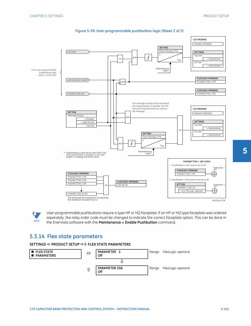
CHAPTER 5: SETTINGS PRODUCT SETUP
C70 CAPACITOR BANK PROTECTION AND CONTROL SYSTEM – INSTRUCTION MANUAL 5-101
5
Figure 5-39: User-programmable pushbutton logic (Sheet 2 of 2)
5.3.14 Flex state parametersSETTINGS PRODUCT SETUP FLEX STATE PARAMETERS
NOTE
User-programmable pushbuttons require a type HP or HQ faceplate. If an HP or HQ type faceplate was ordered separately, the relay order code must be changed to indicate the correct faceplate option. This can be done in the EnerVista software with the Maintenance > Enable Pushbutton command.
FLEX STATE PARAMETERS PARAMETER 1:
OffRange: FlexLogic operand
PARAMETER 256:Off
Range: FlexLogic operand

5-102 C70 CAPACITOR BANK PROTECTION AND CONTROL SYSTEM – INSTRUCTION MANUAL
PRODUCT SETUP CHAPTER 5: SETTINGS
5
This feature provides a mechanism where any of 256 selected FlexLogic operand states can be used for efficient monitoring. The feature allows user-customized access to the FlexLogic operand states in the relay. The state bits are packed so that 16 states are readable in a single Modbus register. The state bits can be configured so that all states of interest are available in a minimum number of Modbus registers.
The state bits can be read out in the “Flex States” register array beginning at Modbus address 0900h. Sixteen states are packed into each register, with the lowest-numbered state in the lowest-order bit. Sixteen registers accommodate the 256 state bits.
5.3.15 User-definable displays
5.3.15.1 MenuSETTINGS PRODUCT SETUP USER-DEFINABLE DISPLAYS
This menu provides a mechanism for manually creating up to 16 user-defined information displays in a convenient viewing sequence in the USER DISPLAY menu (between the TARGETS and ACTUAL VALUES top-level menus). The sub-menus facilitate text entry and Modbus register data pointer options for defining the user display content.
Once programmed, the user-definable displays can be viewed in two ways.
• Keypad — Use the MENU key to select the USER DISPLAY menu item to access the first user-definable display (note that only the programmed screens are displayed). The screens can be scrolled using the up and down arrow keys. The display disappears after the default message time-out period specified by the PRODUCT SETUP DISPLAY PROPERTIES DEFAULT MESSAGE TIMEOUT setting.
• User-programmable control input — The user-definable displays also respond to the INVOKE AND SCROLL setting. Any FlexLogic operand (in particular, the user-programmable pushbutton operands), can be used to navigate the programmed displays.
On the rising edge of the configured operand (such as when the pushbutton is pressed), the displays are invoked by showing the last user-definable display shown during the previous activity. From this moment onward, the operand acts exactly as the down key and allows scrolling through the configured displays. The last display wraps up to the first one. The INVOKE AND SCROLL input and the down arrow key operate concurrently.
When the default timer expires (set by the DEFAULT MESSAGE TIMEOUT setting), the relay starts to cycle through the user displays. The next activity of the INVOKE AND SCROLL input stops the cycling at the currently displayed user display, not at the first user-defined display. The INVOKE AND SCROLL pulses must last for at least 250 ms to take effect.
5.3.15.2 User display 1(16)SETTINGS PRODUCT SETUP USER-DEFINABLE DISPLAYS USER DISPLAY 1(16)
USER-DEFINABLE DISPLAYS INVOKE AND SCROLL:
OffRange: FlexLogic operand
USER DISPLAY 1
See below
USER DISPLAY 16
USER DISPLAY 1 DISP 1 TOP LINE: Range: up to 20 alphanumeric characters
DISP 1 BOTTOM LINE: Range: up to 20 alphanumeric characters
DISP 1 ITEM 10
Range: 0 to 65535 in steps of 1

CHAPTER 5: SETTINGS PRODUCT SETUP
C70 CAPACITOR BANK PROTECTION AND CONTROL SYSTEM – INSTRUCTION MANUAL 5-103
5
Any existing system display can be automatically copied into an available user display by selecting the existing display and pressing the ENTER key. The display then prompts with ADD TO USER DISPLAY LIST? After selecting “Yes,” a message indicates that the selected display has been added to the user display list. When this type of entry occurs, the sub-menus are automatically configured with the proper content—this content can be edited subsequently.
This menu is used to enter user-defined text and user-selected Modbus-registered data fields into the particular user display. Each user display consists of two 20-character lines (top and bottom). The tilde (~) character is used to mark the start of a data field – the length of the data field needs to be accounted for. Up to five separate data fields can be entered in a user display – the nth tilde (~) refers to the nth item.
A user display can be entered from the faceplate keypad or the EnerVista interface (preferred for convenience). The following procedure shows how to enter text characters in the top and bottom lines from the faceplate keypad:
1. Select the line to be edited.
2. Press the decimal key to enter text edit mode.
3. Use either VALUE key to scroll through the characters. A space is selected like a character.
4. Press the decimal key to advance the cursor to the next position.
5. Repeat step 3 and continue entering characters until the desired text is displayed.
6. The HELP key can be pressed at any time for context sensitive help information.
7. Press the ENTER key to store the new settings.
To enter a numerical value for any of the five items (the decimal form of the selected Modbus address) from the faceplate keypad, use the number keypad. Use the value of “0” for any items not being used. Use the HELP key at any selected system display (setting, actual value, or command) which has a Modbus address, to view the hexadecimal form of the Modbus address, then manually convert it to decimal form before entering it (EnerVista usage conveniently facilitates this conversion).
Use the MENU key to go to the user displays menu to view the user-defined content. The current user displays show in sequence, changing every four seconds. While viewing a user display, press the ENTER key and then select the ‘Yes” option to remove the display from the user display list. Use the MENU key again to exit the user displays menu.
An example of user display setup and result is shown as follows.
If the parameters for the top line and the bottom line items have the same units, then the unit is displayed on the bottom line only. The units are only displayed on both lines if the units specified both the top and bottom line items are different.
DISP 1 ITEM 5:0
Range: 0 to 65535 in steps of 1
USER DISPLAY 1 DISP 1 TOP LINE:
Current X ~ AShows user-defined text with first tilde marker
DISP 1 BOTTOM LINE:Current Y ~ A
Shows user-defined text with second tilde marker
DISP 1 ITEM 1:6016
Shows decimal form of user-selected Modbus register address, corresponding to first tilde marker
DISP 1 ITEM 2:6357
Shows decimal form of user-selected Modbus register address, corresponding to second tilde marker
DISP 1 ITEM 3:0
This item is not being used. There is no corresponding tilde marker in top or bottom lines.
DISP 1 ITEM 4:0
This item is not being used. There is no corresponding tilde marker in top or bottom lines.
DISP 1 ITEM 5:0
This item is not being used. There is no corresponding tilde marker in top or bottom lines.
USER DISPLAYS Current X 0.850Current Y 0.327 A
Shows the resultant display content
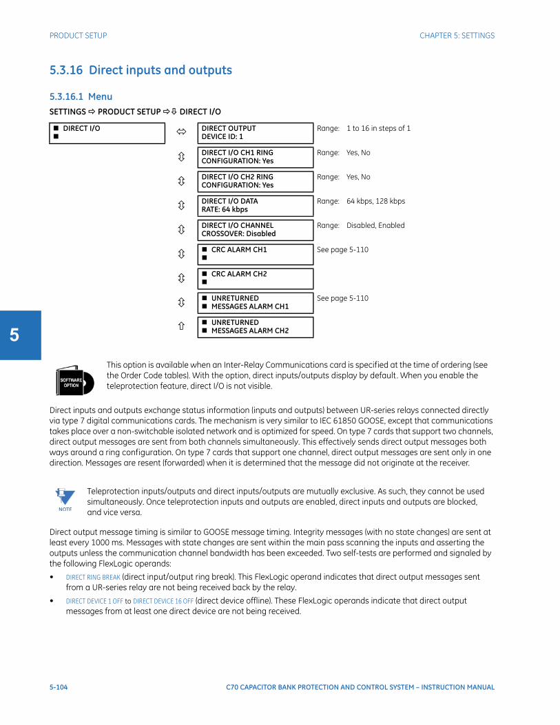
5-104 C70 CAPACITOR BANK PROTECTION AND CONTROL SYSTEM – INSTRUCTION MANUAL
PRODUCT SETUP CHAPTER 5: SETTINGS
5
5.3.16 Direct inputs and outputs
5.3.16.1 MenuSETTINGS PRODUCT SETUP DIRECT I/O
Direct inputs and outputs exchange status information (inputs and outputs) between UR-series relays connected directly via type 7 digital communications cards. The mechanism is very similar to IEC 61850 GOOSE, except that communications takes place over a non-switchable isolated network and is optimized for speed. On type 7 cards that support two channels, direct output messages are sent from both channels simultaneously. This effectively sends direct output messages both ways around a ring configuration. On type 7 cards that support one channel, direct output messages are sent only in one direction. Messages are resent (forwarded) when it is determined that the message did not originate at the receiver.
Direct output message timing is similar to GOOSE message timing. Integrity messages (with no state changes) are sent at least every 1000 ms. Messages with state changes are sent within the main pass scanning the inputs and asserting the outputs unless the communication channel bandwidth has been exceeded. Two self-tests are performed and signaled by the following FlexLogic operands:
• DIRECT RING BREAK (direct input/output ring break). This FlexLogic operand indicates that direct output messages sent from a UR-series relay are not being received back by the relay.
• DIRECT DEVICE 1 OFF to DIRECT DEVICE 16 OFF (direct device offline). These FlexLogic operands indicate that direct output messages from at least one direct device are not being received.
DIRECT I/O DIRECT OUTPUT
DEVICE ID: 1Range: 1 to 16 in steps of 1
DIRECT I/O CH1 RINGCONFIGURATION: Yes
Range: Yes, No
DIRECT I/O CH2 RINGCONFIGURATION: Yes
Range: Yes, No
DIRECT I/O DATARATE: 64 kbps
Range: 64 kbps, 128 kbps
DIRECT I/O CHANNELCROSSOVER: Disabled
Range: Disabled, Enabled
CRC ALARM CH1
See page 5-110
CRC ALARM CH2
UNRETURNED MESSAGES ALARM CH1
See page 5-110
UNRETURNED MESSAGES ALARM CH2
This option is available when an Inter-Relay Communications card is specified at the time of ordering (see the Order Code tables). With the option, direct inputs/outputs display by default. When you enable the teleprotection feature, direct I/O is not visible.
NOTE
Teleprotection inputs/outputs and direct inputs/outputs are mutually exclusive. As such, they cannot be used simultaneously. Once teleprotection inputs and outputs are enabled, direct inputs and outputs are blocked, and vice versa.
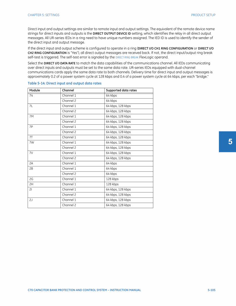
CHAPTER 5: SETTINGS PRODUCT SETUP
C70 CAPACITOR BANK PROTECTION AND CONTROL SYSTEM – INSTRUCTION MANUAL 5-105
5
Direct input and output settings are similar to remote input and output settings. The equivalent of the remote device name strings for direct inputs and outputs is the DIRECT OUTPUT DEVICE ID setting, which identifies the relay in all direct output messages. All UR-series IEDs in a ring need to have unique numbers assigned. The IED ID is used to identify the sender of the direct input and output message.
If the direct input and output scheme is configured to operate in a ring (DIRECT I/O CH1 RING CONFIGURATION or DIRECT I/O CH2 RING CONFIGURATION is “Yes”), all direct output messages are received back. If not, the direct input/output ring break self-test is triggered. The self-test error is signaled by the DIRECT RING BREAK FlexLogic operand.
Select the DIRECT I/O DATA RATE to match the data capabilities of the communications channel. All IEDs communicating over direct inputs and outputs must be set to the same data rate. UR-series IEDs equipped with dual-channel communications cards apply the same data rate to both channels. Delivery time for direct input and output messages is approximately 0.2 of a power system cycle at 128 kbps and 0.4 of a power system cycle at 64 kbps, per each "bridge."
Table 5-14: Direct input and output data rates
Module Channel Supported data rates
74 Channel 1 64 kbps
Channel 2 64 kbps
7L Channel 1 64 kbps, 128 kbps
Channel 2 64 kbps, 128 kbps
7M Channel 1 64 kbps, 128 kbps
Channel 2 64 kbps, 128 kbps
7P Channel 1 64 kbps, 128 kbps
Channel 2 64 kbps, 128 kbps
7T Channel 1 64 kbps, 128 kbps
7W Channel 1 64 kbps, 128 kbps
Channel 2 64 kbps, 128 kbps
7V Channel 1 64 kbps, 128 kbps
Channel 2 64 kbps, 128 kbps
2A Channel 1 64 kbps
2B Channel 1 64 kbps
Channel 2 64 kbps
2G Channel 1 128 kbps
2H Channel 1 128 kbps
2I Channel 1 64 kbps, 128 kbps
Channel 2 64 kbps, 128 kbps
2J Channel 1 64 kbps, 128 kbps
Channel 2 64 kbps, 128 kbps
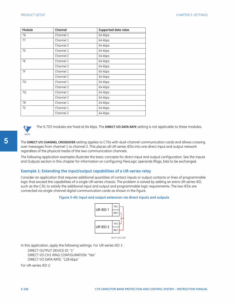
5-106 C70 CAPACITOR BANK PROTECTION AND CONTROL SYSTEM – INSTRUCTION MANUAL
PRODUCT SETUP CHAPTER 5: SETTINGS
5 The DIRECT I/O CHANNEL CROSSOVER setting applies to C70s with dual-channel communication cards and allows crossing over messages from channel 1 to channel 2. This places all UR-series IEDs into one direct input and output network regardless of the physical media of the two communication channels.
The following application examples illustrate the basic concepts for direct input and output configuration. See the Inputs and Outputs section in this chapter for information on configuring FlexLogic operands (flags, bits) to be exchanged.
Example 1: Extending the input/output capabilities of a UR-series relayConsider an application that requires additional quantities of contact inputs or output contacts or lines of programmable logic that exceed the capabilities of a single UR-series chassis. The problem is solved by adding an extra UR-series IED, such as the C30, to satisfy the additional input and output and programmable logic requirements. The two IEDs are connected via single-channel digital communication cards as shown in the figure.
Figure 5-40: Input and output extension via direct inputs and outputs
In this application, apply the following settings. For UR-series IED 1:DIRECT OUTPUT DEVICE ID: “1”DIRECT I/O CH1 RING CONFIGURATION: “Yes”DIRECT I/O DATA RATE: “128 kbps”
For UR-series IED 2:
76 Channel 1 64 kbps
77 Channel 1 64 kbps
Channel 2 64 kbps
75 Channel 1 64 kbps
Channel 2 64 kbps
7E Channel 1 64 kbps
Channel 2 64 kbps
7F Channel 1 64 kbps
Channel 2 64 kbps
7G Channel 1 64 kbps
Channel 2 64 kbps
7Q Channel 1 64 kbps
Channel 2 64 kbps
7R Channel 1 64 kbps
7S Channel 1 64 kbps
Channel 2 64 kbps
NOTE
The G.703 modules are fixed at 64 kbps. The DIRECT I/O DATA RATE setting is not applicable to these modules.
Module Channel Supported data rates

CHAPTER 5: SETTINGS PRODUCT SETUP
C70 CAPACITOR BANK PROTECTION AND CONTROL SYSTEM – INSTRUCTION MANUAL 5-107
5
DIRECT OUTPUT DEVICE ID: “2”DIRECT I/O CH1 RING CONFIGURATION: “Yes”DIRECT I/O DATA RATE: “128 kbps”
The message delivery time is about 0.2 of power cycle in both ways (at 128 kbps); that is, from device 1 to device 2, and from device 2 to device 1. Different communications cards can be selected by the user for this back-to-back connection (for example: fiber, G.703, or RS422).
Example 2: Interlocking busbar protectionA simple interlocking busbar protection scheme could be accomplished by sending a blocking signal from downstream devices, say 2, 3, and 4, to the upstream device that monitors a single incomer of the busbar, as shown.
Figure 5-41: Sample interlocking busbar protection scheme
For increased reliability, a dual-ring configuration (shown as follows) is recommended for this application.
Figure 5-42: Interlocking bus protection scheme via direct inputs/outputs
In this application, apply the following settings. For UR-series IED 1:DIRECT OUTPUT DEVICE ID: “1”DIRECT I/O CH1 RING CONFIGURATION: “Yes”DIRECT I/O CH2 RING CONFIGURATION: “Yes”
For UR-series IED 2:DIRECT OUTPUT DEVICE ID: “2”DIRECT I/O CH1 RING CONFIGURATION: “Yes”DIRECT I/O CH2 RING CONFIGURATION: “Yes”
For UR-series IED 3:DIRECT OUTPUT DEVICE ID: “3”DIRECT I/O CH1 RING CONFIGURATION: “Yes”DIRECT I/O CH2 RING CONFIGURATION: “Yes”
For UR-series IED 4:DIRECT OUTPUT DEVICE ID: “4”DIRECT I/O CH1 RING CONFIGURATION: “Yes”DIRECT I/O CH2 RING CONFIGURATION: “Yes”
842712A1.CDR
UR IED 1
UR IED 2 UR IED 4UR IED 3
BLOCK
842716A1.CDR
UR IED 1RX1
TX2
TX1
RX2
UR IED 2TX2
RX2
RX1
TX1
UR IED 4TX1
RX1
RX2
TX2
UR IED 3RX2
TX1
TX2
RX1

5-108 C70 CAPACITOR BANK PROTECTION AND CONTROL SYSTEM – INSTRUCTION MANUAL
PRODUCT SETUP CHAPTER 5: SETTINGS
5
Message delivery time is approximately 0.2 of power system cycle (at 128 kbps) times number of ‘bridges’ between the origin and destination. Dual-ring configuration effectively reduces the maximum ‘communications distance’ by a factor of two.
In this configuration the following delivery times are expected (at 128 kbps) if both rings are healthy:IED 1 to IED 2: 0.2 of power system cycleIED 1 to IED 3: 0.4 of power system cycleIED 1 to IED 4: 0.2 of power system cycleIED 2 to IED 3: 0.2 of power system cycleIED 2 to IED 4: 0.4 of power system cycleIED 3 to IED 4: 0.2 of power system cycle
If one ring is broken (say TX2-RX2) the delivery times are as follows:IED 1 to IED 2: 0.2 of power system cycleIED 1 to IED 3: 0.4 of power system cycleIED 1 to IED 4: 0.6 of power system cycleIED 2 to IED 3: 0.2 of power system cycleIED 2 to IED 4: 0.4 of power system cycleIED 3 to IED 4: 0.2 of power system cycle
A coordinating timer for this bus protection scheme could be selected to cover the worst case scenario (0.4 of a power system cycle). Upon detecting a broken ring, the coordination time is adaptively increased to 0.6 of a power system cycle. The complete application requires addressing a number of issues, such as failure of both the communications rings, failure or out-of-service conditions of one of the relays, and so on. Self-monitoring flags of the direct inputs and outputs feature primarily are used to address these concerns.
Example 3: Pilot-aided schemesConsider the three-terminal line protection application shown.
Figure 5-43: Three-terminal line application
A permissive pilot-aided scheme can be implemented in a two-ring configuration, shown as follows (IEDs 1 and 2 constitute a first ring, while IEDs 2 and 3 constitute a second ring).
Figure 5-44: Single-channel open loop configuration
842713A1.CDR
UR IED 1 UR IED 2
UR IED 3
842714A1.CDR
UR IED 1TX1
RX1
UR IED 2RX2
TX2
RX1
TX1
UR IED 3RX1
TX1
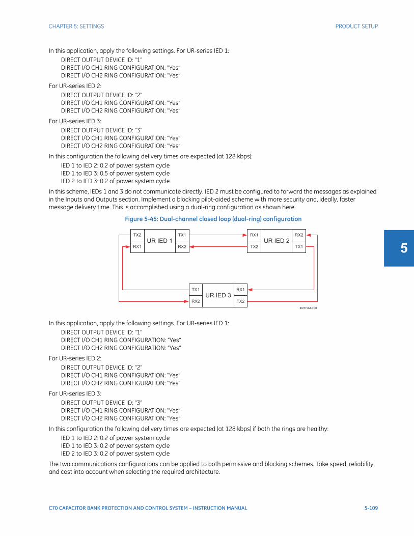
CHAPTER 5: SETTINGS PRODUCT SETUP
C70 CAPACITOR BANK PROTECTION AND CONTROL SYSTEM – INSTRUCTION MANUAL 5-109
5
In this application, apply the following settings. For UR-series IED 1:DIRECT OUTPUT DEVICE ID: “1”DIRECT I/O CH1 RING CONFIGURATION: “Yes”DIRECT I/O CH2 RING CONFIGURATION: “Yes”
For UR-series IED 2:DIRECT OUTPUT DEVICE ID: “2”DIRECT I/O CH1 RING CONFIGURATION: “Yes”DIRECT I/O CH2 RING CONFIGURATION: “Yes”
For UR-series IED 3:DIRECT OUTPUT DEVICE ID: “3”DIRECT I/O CH1 RING CONFIGURATION: “Yes”DIRECT I/O CH2 RING CONFIGURATION: “Yes”
In this configuration the following delivery times are expected (at 128 kbps):IED 1 to IED 2: 0.2 of power system cycleIED 1 to IED 3: 0.5 of power system cycleIED 2 to IED 3: 0.2 of power system cycle
In this scheme, IEDs 1 and 3 do not communicate directly. IED 2 must be configured to forward the messages as explained in the Inputs and Outputs section. Implement a blocking pilot-aided scheme with more security and, ideally, faster message delivery time. This is accomplished using a dual-ring configuration as shown here.
Figure 5-45: Dual-channel closed loop (dual-ring) configuration
In this application, apply the following settings. For UR-series IED 1:DIRECT OUTPUT DEVICE ID: “1”DIRECT I/O CH1 RING CONFIGURATION: “Yes”DIRECT I/O CH2 RING CONFIGURATION: “Yes”
For UR-series IED 2:DIRECT OUTPUT DEVICE ID: “2”DIRECT I/O CH1 RING CONFIGURATION: “Yes”DIRECT I/O CH2 RING CONFIGURATION: “Yes”
For UR-series IED 3:DIRECT OUTPUT DEVICE ID: “3”DIRECT I/O CH1 RING CONFIGURATION: “Yes”DIRECT I/O CH2 RING CONFIGURATION: “Yes”
In this configuration the following delivery times are expected (at 128 kbps) if both the rings are healthy:IED 1 to IED 2: 0.2 of power system cycleIED 1 to IED 3: 0.2 of power system cycleIED 2 to IED 3: 0.2 of power system cycle
The two communications configurations can be applied to both permissive and blocking schemes. Take speed, reliability, and cost into account when selecting the required architecture.
842715A1.CDR
UR IED 1TX1
RX2
TX2
RX1
UR IED 2RX2
TX1
RX1
TX2
UR IED 3RX1
TX2
TX1
RX2

5-110 C70 CAPACITOR BANK PROTECTION AND CONTROL SYSTEM – INSTRUCTION MANUAL
PRODUCT SETUP CHAPTER 5: SETTINGS
5
5.3.16.2 CRC alarm CH1(2)SETTINGS PRODUCT SETUP DIRECT I/O CRC ALARM CH1(2)
The C70 checks integrity of the incoming direct input and output messages using a 32-bit CRC. The CRC alarm function is available for monitoring the communication medium noise by tracking the rate of messages failing the CRC check. The monitoring function counts all incoming messages, including messages that failed the CRC check. A separate counter adds up messages that failed the CRC check. When the failed CRC counter reaches the user-defined level specified by the CRC ALARM CH1 THRESHOLD setting within the user-defined message count CRC ALARM 1 CH1 COUNT, the DIR IO CH1 CRC ALARM FlexLogic operand is set.
When the total message counter reaches the user-defined maximum specified by the CRC ALARM CH1 MESSAGE COUNT setting, both the counters reset and the monitoring process is restarted.
Configure the operand to drive an output contact, user-programmable LED, or selected communication-based output. Latching and acknowledging conditions—if required—are programmed accordingly.
The CRC alarm function is available on a per-channel basis. The total number of direct input and output messages that failed the CRC check is available as the ACTUAL VALUES STATUS DIRECT INPUTS CRC FAIL COUNT CH1 actual value.
• Message count and length of the monitoring window — To monitor communications integrity, the relay sends 1 message per second (at 64 kbps) or 2 messages per second (128 kbps) even if there is no change in the direct outputs. For example, setting the CRC ALARM CH1 MESSAGE COUNT to “10000,” corresponds a time window of about 160 minutes at 64 kbps and 80 minutes at 128 kbps. If the messages are sent faster as a result of direct outputs activity, the monitoring time interval shortens. Take this into account when determining the CRC ALARM CH1 MESSAGE COUNT setting. For example, if the requirement is a maximum monitoring time interval of 10 minutes at 64 kbps, then the CRC ALARM CH1 MESSAGE COUNT is set to 10 × 60 × 1 = 600.
• Correlation of failed CRC and bit error rate (BER) — The CRC check can fail if one or more bits in a packet are corrupted. Therefore, an exact correlation between the CRC fail rate and the BER is not possible. Under certain assumptions an approximation can be made as follows. A direct input and output packet containing 20 bytes results in 160 bits of data being sent and therefore, a transmission of 63 packets is equivalent to 10,000 bits. A BER of 10–4 implies 1 bit error for every 10000 bits sent or received. Assuming the best case of only 1 bit error in a failed packet, having 1 failed packet for every 63 received is about equal to a BER of 10–4.
5.3.16.3 Unreturned messages alarm CH1(2)SETTINGS PRODUCT SETUP DIRECT I/O UNRETURNED MESSAGES ALARM CH1(2)
The C70 checks integrity of the direct input and output communication ring by counting unreturned messages. In the ring configuration, all messages originating at a given device should return within a pre-defined period of time. The unreturned messages alarm function is available for monitoring the integrity of the communication ring by tracking the rate of
CRC ALARM CH1 CRC ALARM CH1
FUNCTION: DisabledRange: Enabled, Disabled
CRC ALARM CH1MESSAGE COUNT: 600
Range: 100 to 10000 in steps of 1
CRC ALARM CH1THRESHOLD: 10
Range: 1 to 1000 in steps of 1
CRC ALARM CH1EVENTS: Disabled
Range: Enabled, Disabled
UNRETURNED MESSAGES ALARM CH1 UNRET MSGS ALARM CH1
FUNCTION: DisabledRange: Enabled, Disabled
UNRET MSGS ALARM CH1MESSAGE COUNT: 600
Range: 100 to 10000 in steps of 1
UNRET MSGS ALARM CH1THRESHOLD: 10
Range: 1 to 1000 in steps of 1
UNRET MSGS ALARM CH1EVENTS: Disabled
Range: Enabled, Disabled
CHAPTER 5: SETTINGS REMOTE RESOURCES
C70 CAPACITOR BANK PROTECTION AND CONTROL SYSTEM – INSTRUCTION MANUAL 5-111
5
unreturned messages. This function counts all the outgoing messages and a separate counter adds the messages have failed to return. When the unreturned messages counter reaches the user-definable level specified by the UNRET MSGS ALARM CH1 THRESHOLD setting and within the user-defined message count UNRET MSGS ALARM CH1 COUNT, the DIR IO CH1 UNRET ALM FlexLogic operand is set.
When the total message counter reaches the user-defined maximum specified by the UNRET MSGS ALARM CH1 MESSAGE COUNT setting, both the counters reset and the monitoring process is restarted.
Configure the operand to drive an output contact, user-programmable LED, or selected communication-based output. Latching and acknowledging conditions, if required, are programmed accordingly.
The unreturned messages alarm function is available on a per-channel basis and is active only in the ring configuration. The total number of unreturned input and output messages is available as the ACTUAL VALUES STATUS DIRECT INPUTS UNRETURNED MSG COUNT CH1 actual value.
5.3.17 InstallationSETTINGS PRODUCT SETUP INSTALLATION
To safeguard against the installation of a relay without any entered settings, the unit does not allow signaling of any output relay until RELAY SETTINGS is set to "Programmed." This setting is "Not Programmed" by default. The UNIT NOT PROGRAMMED self-test error message displays until the relay is put into the "Programmed" state.
The RELAY NAME setting allows the user to uniquely identify a relay. This name appears on generated reports.
5.4 Remote resources
5.4.1 Remote resources configurationWhen the C70 is ordered with a process card module as a part of HardFiber system, an additional Remote Resources menu tree is available in the EnerVista software to allow configuration of the HardFiber system.
Figure 5-46: Remote Resources configuration menu
INSTALLATION RELAY SETTINGS:
Not ProgrammedRange: Not Programmed, Programmed
RELAY NAME:Relay-1
Range: up to 20 alphanumeric characters

5-112 C70 CAPACITOR BANK PROTECTION AND CONTROL SYSTEM – INSTRUCTION MANUAL
SYSTEM SETUP CHAPTER 5: SETTINGS
5
The remote resources settings configure a C70 with a process bus module to work with HardFiber Bricks. Remote resources configuration is only available through the EnerVista software, and is not available through the C70 front panel. A Brick provides eight AC measurements, along with contact inputs, DC analog inputs, and contact outputs, to be the remote interface to field equipment such as circuit breakers and transformers. The C70 with a process bus module has access to all of the capabilities of up to eight Bricks. Remote resources settings configure the point-to-point connection between specific fiber optic ports on the C70 process card and specific Brick. The relay is then configured to measure specific currents, voltages and contact inputs from those Bricks, and to control specific outputs.
The configuration process for remote resources is straightforward and consists of the following steps.
• Configure the field units. This establishes the point-to-point connection between a specific port on the relay process bus module, and a specific digital core on a specific Brick. This is a necessary first step in configuring a process bus relay.
• Configure the AC banks. This sets the primary and secondary quantities and connections for currents and voltages. AC bank configuration also provides a provision for redundant measurements for currents and voltages, a powerful reliability improvement possible with process bus.
• Configure signal sources. This functionality of the C70 has not changed other than the requirement to use currents and voltages established by AC bank configuration under the remote resources menu.
• Configure field contact inputs, field contact outputs, RTDs, and transducers as required for the application's functionality. These inputs and outputs are the physical interface to circuit breakers, transformers, and other equipment. They replace the traditional contact inputs and outputs located at the relay to virtually eliminate copper wiring.
• Configure shared inputs and outputs as required for the application's functionality. Shared inputs and outputs are distinct binary channels that provide high-speed protection quality signaling between relays through a Brick.
For additional information on how to configure a relay with a process bus module, see the HardFiber Process Bus System Instruction Manual.
5.5 System setup
5.5.1 AC inputs
5.5.1.1 Current banksSETTINGS SYSTEM SETUP AC INPUTS CURRENT BANK F1(U5)
Six banks of phase and ground CTs can be set, where the current banks are denoted in the following format (X represents the module slot position letter):
Xa, where X = F, M, U and a = 1, 5
See the Introduction to AC Sources section at the beginning of this chapter for details.
These settings are critical for all features that have settings dependent on current measurements. When the relay is ordered, the CT module must be specified to include a standard or sensitive ground input. As the phase CTs are connected in wye (star), the calculated phasor sum of the three phase currents (IA + IB + IC = neutral current = 3Io) is used as the input for the neutral overcurrent elements. In addition, a zero-sequence (core balance) CT which senses current in all of the
CURRENT BANK F1 PHASE CT F1
PRIMARY: 1 ARange: 1 to 65000 A in steps of 1
PHASE CT F1SECONDARY: 1 A
Range: 1 A, 5 A
GROUND CT F1PRIMARY: 1 A
Range: 1 to 65000 A in steps of 1
GROUND CT F1SECONDARY: 1 A
Range: 1 A, 5 A

CHAPTER 5: SETTINGS SYSTEM SETUP
C70 CAPACITOR BANK PROTECTION AND CONTROL SYSTEM – INSTRUCTION MANUAL 5-113
5
circuit primary conductors, or a CT in a neutral grounding conductor can also be used. For this configuration, the ground CT primary rating must be entered. To detect low level ground fault currents, the sensitive ground input can be used. In this case, the sensitive ground CT primary rating must be entered. See chapter 3 for more details on CT connections.
Enter the rated CT primary current values. For both 1000:5 and 1000:1 CTs, the entry would be 1000. For correct operation, the CT secondary rating must match the setting (which must also correspond to the specific CT connections used).
The following example illustrates how multiple CT inputs (current banks) are summed as one source current. Given the following current banks:
• F1: CT bank with 500:1 ratio
• F5: CT bank with 1000:1 ratio
• M1: CT bank with 800:1 ratio
The following rule applies:
Eq. 5-6
1 pu is the highest primary current. In this case, 1000 is entered and the secondary current from the 500:1 ratio CT is adjusted to that created by a 1000:1 CT before summation. If a protection element is set up to act on SRC 1 currents, then a pickup level of 1 pu operates on 1000 A primary.
The same rule applies for current sums from CTs with different secondary taps (5 A and 1 A).
5.5.1.2 Voltage banksSETTINGS SYSTEM SETUP AC INPUTS VOLTAGE BANK F5(U5)
Three bank of phase/auxiliary VTs can be set, where voltage banks are denoted in the following format (X represents the module slot position letter):
Xa, where X = F, M, U and a = 5
See the Introduction to AC Sources section at the beginning of this chapter for additional details.
With VTs installed, the relay can perform voltage measurements as well as power calculations. Enter the PHASE VT F5 CONNECTION made to the system as “Wye” or “Delta.” An open-delta source VT connection is entered as “Delta.”
VOLTAGE BANK F5 PHASE VT F5
CONNECTION: WyeRange: Wye, Delta
PHASE VT F5SECONDARY: 66.4 V
Range: 25.0 to 240.0 V in steps of 0.1
PHASE VT F5RATIO: 1.00 :1
Range: 1.00 to 24000.00 in steps of 0.01
AUXILIARY VT F5CONNECTION: Vag
Range: Vn, Vag, Vbg, Vcg, Vab, Vbc, Vca
AUXILIARY VT F5SECONDARY: 66.4 V
Range: 25.0 to 240.0 V in steps of 0.1
AUXILIARY VT F5RATIO: 1.00 :1
Range: 1.00 to 24000.00 in steps of 0.01
NOTE
The nominal PHASE VT F5 SECONDARY voltage setting is the voltage across the relay input terminals when nominal voltage is applied to the VT primary.For example, on a system with a 13.8 kV nominal primary voltage and with a 14400:120 volt VT in a delta connection, the secondary voltage is 115; that is, (13800 / 14400) × 120. For a wye connection, the voltage value entered must be the phase to neutral voltage, which is 115 / = 66.4.On a 14.4 kV system with a delta connection and a VT primary to secondary turns ratio of 14400:120, the voltage value entered is 120; that is, 14400 / 120.
SRC 1 F1 F5 M1+ +=
3

5-114 C70 CAPACITOR BANK PROTECTION AND CONTROL SYSTEM – INSTRUCTION MANUAL
SYSTEM SETUP CHAPTER 5: SETTINGS
5
5.5.2 Power systemSETTINGS SYSTEM SETUP POWER SYSTEM
The power system NOMINAL FREQUENCY value is used as a default to set the digital sampling rate if the system frequency cannot be measured from available signals. This can happen if the signals are not present or are heavily distorted. Before reverting to the nominal frequency, the frequency tracking algorithm holds the last valid frequency measurement for a safe period of time while waiting for the signals to reappear or for the distortions to decay.
The phase sequence of the power system is required to properly calculate sequence components and power parameters. The PHASE ROTATION setting matches the power system phase sequence and informs the relay of the actual system phase sequence, either ABC or ACB. CT and VT inputs on the relay, labeled as A, B, and C, must be connected to system phases A, B, and C for correct operation.
The FREQUENCY AND PHASE REFERENCE setting determines which signal source is used (and hence which AC signal) for phase angle reference. The AC signal used is prioritized based on the AC inputs configured for the signal source. Phase voltages takes precedence, followed by auxiliary voltage, then phase currents, and finally ground current.
For three phase selection, phase A is used for angle referencing ( ), while Clarke transformation of the phase signals is used for frequency metering and tracking ( ) for better performance during fault, open pole, and VT and CT fail conditions.
The phase reference and frequency tracking AC signals are selected based upon the source configuration, regardless of whether or not a particular signal is actually applied to the relay.
Phase angle of the reference signal always displays zero degrees and all other phase angles are relative to this signal. If the pre-selected reference signal is not measurable at a given time, the phase angles are not referenced.
The phase angle referencing is done via a phase locked loop, which can synchronize independent UR-series relays if they have the same AC signal reference. This results in very precise correlation of phase angle indications between different UR-series relays.
FREQUENCY TRACKING is set to “Disabled” only in unusual circumstances; consult GE Digital Energy for special variable-frequency applications.
5.5.3 Signal sourcesSETTINGS SYSTEM SETUP SIGNAL SOURCES SOURCE 1(6)
NOTE
If the PHASE VT F5 CONNECTION is set to “Delta”, the relay does not calculate voltage harmonics.
POWER SYSTEM NOMINAL FREQUENCY:
60 HzRange: 25 to 60 Hz in steps of 1
PHASE ROTATION:ABC
Range: ABC, ACB
FREQUENCY AND PHASEREFERENCE: SRC 1
Range: SRC 1, SRC 2, SRC 3, SRC 4, SRC 5, SRC 6
FREQUENCYTRACKING:Enabled
Range: Disabled, Enabled
NOTE
The frequency tracking feature functions only when the C70 is in the “Programmed” mode. If the C70 is “Not Programmed,” then metering values are available but can exhibit significant errors.
SOURCE 1 SOURCE 1 NAME:
SRC 1Range: up to six alphanumeric characters
VANGLE REF VA=VFREQUENCY 2VA VB– VC–( ) 3⁄=
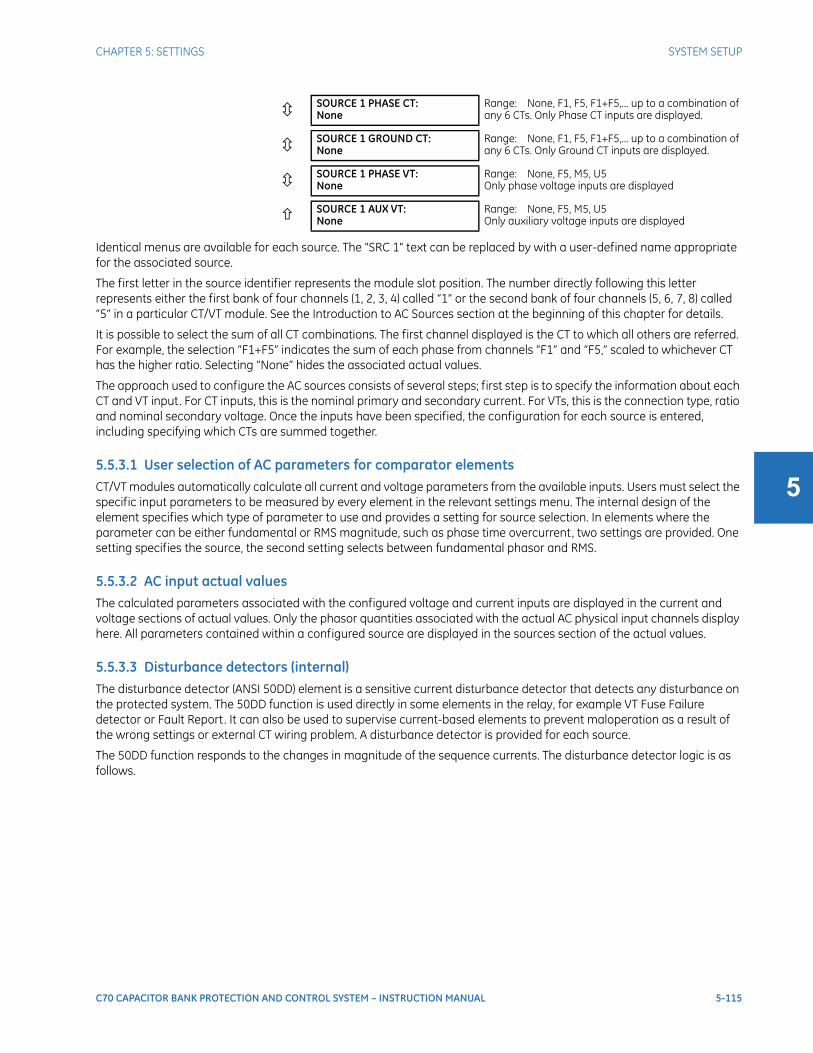
CHAPTER 5: SETTINGS SYSTEM SETUP
C70 CAPACITOR BANK PROTECTION AND CONTROL SYSTEM – INSTRUCTION MANUAL 5-115
5
Identical menus are available for each source. The "SRC 1" text can be replaced by with a user-defined name appropriate for the associated source.
The first letter in the source identifier represents the module slot position. The number directly following this letter represents either the first bank of four channels (1, 2, 3, 4) called “1” or the second bank of four channels (5, 6, 7, 8) called “5” in a particular CT/VT module. See the Introduction to AC Sources section at the beginning of this chapter for details.
It is possible to select the sum of all CT combinations. The first channel displayed is the CT to which all others are referred. For example, the selection “F1+F5” indicates the sum of each phase from channels “F1” and “F5,” scaled to whichever CT has the higher ratio. Selecting “None” hides the associated actual values.
The approach used to configure the AC sources consists of several steps; first step is to specify the information about each CT and VT input. For CT inputs, this is the nominal primary and secondary current. For VTs, this is the connection type, ratio and nominal secondary voltage. Once the inputs have been specified, the configuration for each source is entered, including specifying which CTs are summed together.
5.5.3.1 User selection of AC parameters for comparator elementsCT/VT modules automatically calculate all current and voltage parameters from the available inputs. Users must select the specific input parameters to be measured by every element in the relevant settings menu. The internal design of the element specifies which type of parameter to use and provides a setting for source selection. In elements where the parameter can be either fundamental or RMS magnitude, such as phase time overcurrent, two settings are provided. One setting specifies the source, the second setting selects between fundamental phasor and RMS.
5.5.3.2 AC input actual valuesThe calculated parameters associated with the configured voltage and current inputs are displayed in the current and voltage sections of actual values. Only the phasor quantities associated with the actual AC physical input channels display here. All parameters contained within a configured source are displayed in the sources section of the actual values.
5.5.3.3 Disturbance detectors (internal)The disturbance detector (ANSI 50DD) element is a sensitive current disturbance detector that detects any disturbance on the protected system. The 50DD function is used directly in some elements in the relay, for example VT Fuse Failure detector or Fault Report. It can also be used to supervise current-based elements to prevent maloperation as a result of the wrong settings or external CT wiring problem. A disturbance detector is provided for each source.
The 50DD function responds to the changes in magnitude of the sequence currents. The disturbance detector logic is as follows.
SOURCE 1 PHASE CT:None
Range: None, F1, F5, F1+F5,... up to a combination ofany 6 CTs. Only Phase CT inputs are displayed.
SOURCE 1 GROUND CT:None
Range: None, F1, F5, F1+F5,... up to a combination ofany 6 CTs. Only Ground CT inputs are displayed.
SOURCE 1 PHASE VT:None
Range: None, F5, M5, U5Only phase voltage inputs are displayed
SOURCE 1 AUX VT:None
Range: None, F5, M5, U5Only auxiliary voltage inputs are displayed
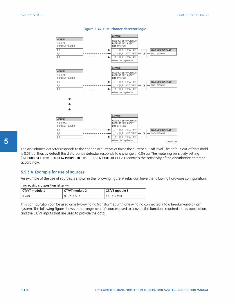
5-116 C70 CAPACITOR BANK PROTECTION AND CONTROL SYSTEM – INSTRUCTION MANUAL
SYSTEM SETUP CHAPTER 5: SETTINGS
5
Figure 5-47: Disturbance detector logic
The disturbance detector responds to the change in currents of twice the current cut-off level. The default cut-off threshold is 0.02 pu; thus by default the disturbance detector responds to a change of 0.04 pu. The metering sensitivity setting (PRODUCT SETUP DISPLAY PROPERTIES CURRENT CUT-OFF LEVEL) controls the sensitivity of the disturbance detector accordingly.
5.5.3.4 Example for use of sourcesAn example of the use of sources is shown in the following figure. A relay can have the following hardware configuration:
This configuration can be used on a two-winding transformer, with one winding connected into a breaker-and-a-half system. The following figure shows the arrangement of sources used to provide the functions required in this application, and the CT/VT inputs that are used to provide the data.
Increasing slot position letter -->
CT/VT module 1 CT/VT module 2 CT/VT module 3
8 CTs 4 CTs, 4 VTs 4 CTs, 4 VTs
827092A3.CDR
SOURCE 1CURRENT PHASOR
PRODUCT SETUP/DISPLAYPROPERTIES/CURRENTCUT-OFF LEVEL
PRODUCT SETUP/DISPLAYPROPERTIES/CURRENTCUT-OFF LEVEL
PRODUCT SETUP/DISPLAYPROPERTIES/CURRENTCUT-OFF LEVEL
SOURCE 2CURRENT PHASOR
SOURCE 6CURRENT PHASOR
ACTUAL
SETTING
SETTING
SETTING
ACTUAL
ACTUAL
FLEXLOGIC OPERAND
FLEXLOGIC OPERAND
FLEXLOGIC OPERAND
I_1
I_1
I_1
SRC 1 50DD OP
SRC 2 50DD OP
SRC 6 50DD OP
I_2
I_2
I_2
I_0
I_0
I_0
OR
OR
OR
Where ’ is 2 cycles oldI
Where ’ is 2 cycles oldI
Where ’ is 2 cycles oldI
I I_1 - _1’ >2*CUT-OFF
I I_1 - _1’ >2*CUT-OFF
I I_1 - _1’ >2*CUT-OFF
I I_2 - _2’ >2*CUT-OFF
I I_2 - _2’ >2*CUT-OFF
I I_2 - _2’ >2*CUT-OFF
I I_0 - _0’ >2*CUT-OFF
I I_0 - _0’ >2*CUT-OFF
I I_0 - _0’ >2*CUT-OFF

CHAPTER 5: SETTINGS SYSTEM SETUP
C70 CAPACITOR BANK PROTECTION AND CONTROL SYSTEM – INSTRUCTION MANUAL 5-117
5
Figure 5-48: Example of use of sources
5.5.4 BreakersSETTINGS SYSTEM SETUP BREAKERS BREAKER 1(6)
Y LV D HV AUX
SRC 1 SRC 2 SRC 3
Phase CT M1 F1+F5 None
Ground CT M1 None None
Phase VT M5 None None
Aux VT None None U1
BREAKER 1 BREAKER 1
FUNCTION: DisabledRange: Disabled, Enabled
BREAKER1 PUSH BUTTONCONTROL: Disabled
Range: Disabled, Enabled
BREAKER 1 NAME:Bkr 1
Range: up to six alphanumeric characters
BREAKER 1 MODE:3-Pole
Range: 3-Pole, 1-Pole
BREAKER 1 OPEN:Off
Range: FlexLogic operand

5-118 C70 CAPACITOR BANK PROTECTION AND CONTROL SYSTEM – INSTRUCTION MANUAL
SYSTEM SETUP CHAPTER 5: SETTINGS
5
A description of the operation of the breaker control and status monitoring features is provided in chapter 4. Information to program the settings is covered here. These features are provided for two or more breakers; a user can use only those portions of the design relevant to a single breaker, which must be breaker 1.
The number of breaker control elements depends on the number of CT/VT modules specified with the C70. The following settings are available for each breaker control element.
BREAKER 1 FUNCTION — This setting enables and disables the operation of the breaker control feature.
BREAKER1 PUSH BUTTON CONTROL — Set to “Enable” to allow faceplate pushbutton operations.
BREAKER 1 NAME — Assign a user-defined name (up to six characters) to the breaker. This name is used in flash messages related to breaker 1.
BREAKER 1 MODE — Selects “3-Pole” mode, where all breaker poles are operated simultaneously, or “1-Pole” mode where all breaker poles are operated either independently or simultaneously.
BREAKER 1 OPEN — Selects an operand that creates a programmable signal to operate an output relay to open breaker 1.
BREAKER 1 BLK OPEN — Selects an operand that prevents opening of the breaker. This setting can be used for select-before-operate functionality or to block operation from a panel switch or from SCADA.
BREAKER 1 CLOSE — Selects an operand that creates a programmable signal to operate an output relay to close breaker 1.
BREAKER 1 BLK CLOSE — Selects an operand that prevents closing of the breaker. This setting can be used for select-before-operate functionality or to block operation from a panel switch or from SCADA.
BREAKER 1 BLK OPEN:Off
Range: FlexLogic operand
BREAKER 1 CLOSE:Off
Range: FlexLogic operand
BREAKER 1 BLK CLOSE:Off
Range: FlexLogic operand
BREAKER 1 ΦA/3P CLSD:Off
Range: FlexLogic operand
BREAKER 1 ΦA/3P OPND:Off
Range: FlexLogic operand
BREAKER 1 ΦB CLOSED:Off
Range: FlexLogic operand
BREAKER 1 ΦB OPENED:Off
Range: FlexLogic operand
BREAKER 1 ΦC CLOSED:Off
Range: FlexLogic operand
BREAKER 1 ΦC OPENED:Off
Range: FlexLogic operand
BREAKER 1 Toperate:0.070 s
Range: 0.000 to 65.535 s in steps of 0.001
BREAKER 1 EXT ALARM:Off
Range: FlexLogic operand
BREAKER 1 ALARMDELAY: 0.000 s
Range: 0.000 to 65.535 s in steps of 0.001
MANUAL CLOSE RECAL1TIME: 0.000 s
Range: 0.000 to 65.535 s in steps of 0.001
BREAKER 1 OUT OF SV:Off
Range: FlexLogic operand
BREAKER 1 EVENTS:Disabled
Range: Disabled, Enabled

CHAPTER 5: SETTINGS SYSTEM SETUP
C70 CAPACITOR BANK PROTECTION AND CONTROL SYSTEM – INSTRUCTION MANUAL 5-119
5
BREAKER 1 ΦA/3P CLOSED — Selects an operand, usually a contact input connected to a breaker auxiliary position tracking mechanism. This input is a normally-open 52/a status input to create a logic 1 when the breaker is closed. If the BREAKER 1 MODE setting is selected as “3-Pole,” this setting selects a single input as the operand used to track the breaker open or closed position. If the mode is selected as “1-Pole,” the input mentioned is used to track phase A and the BREAKER 1 ΦB and BREAKER 1 ΦC settings select operands to track phases B and C, respectively.
BREAKER 1 ΦA/3P OPND — Selects an operand, usually a contact input, that is a normally-closed 52/b status input to create a logic 1 when the breaker is open. If a separate 52/b contact input is not available, then the inverted BREAKER 1 CLOSED status signal can be used.
BREAKER 1 ΦB CLOSED — If the mode is selected as three-pole, this setting has no function. If the mode is selected as single-pole, this input is used to track the breaker phase B closed position as outlined for phase A.
BREAKER 1 ΦB OPENED — If the mode is selected as three-pole, this setting has no function. If the mode is selected as single-pole, this input is used to track the breaker phase B opened position as outlined for phase A.
BREAKER 1 ΦC CLOSED — If the mode is selected as three-pole, this setting has no function. If the mode is selected as single-pole, this input is used to track the breaker phase C closed position as outlined for phase A.
BREAKER 1 ΦC OPENED — If the mode is selected as three-pole, this setting has no function. If the mode is selected as single-pole, this input is used to track the breaker phase C opened position as outlined for phase A.
BREAKER 1 Toperate — This setting specifies the required interval to overcome transient disagreement between the 52/a and 52/b auxiliary contacts during breaker operation. If transient disagreement still exists after this time has expired, the BREAKER 1 BAD STATUS FlexLogic operand is asserted from alarm or blocking purposes.
BREAKER 1 EXT ALARM — This setting selects an operand, usually an external contact input, connected to a breaker alarm reporting contact.
BREAKER 1 ALARM DELAY — This setting specifies the delay interval during which a disagreement of status among the three-pole position tracking operands does not declare a pole disagreement. This allows for non-simultaneous operation of the poles.
MANUAL CLOSE RECAL1 TIME — This setting specifies the interval required to maintain setting changes in effect after an operator has initiated a manual close command to operate a circuit breaker.
BREAKER 1 OUT OF SV — Selects an operand indicating that breaker 1 is out-of-service.
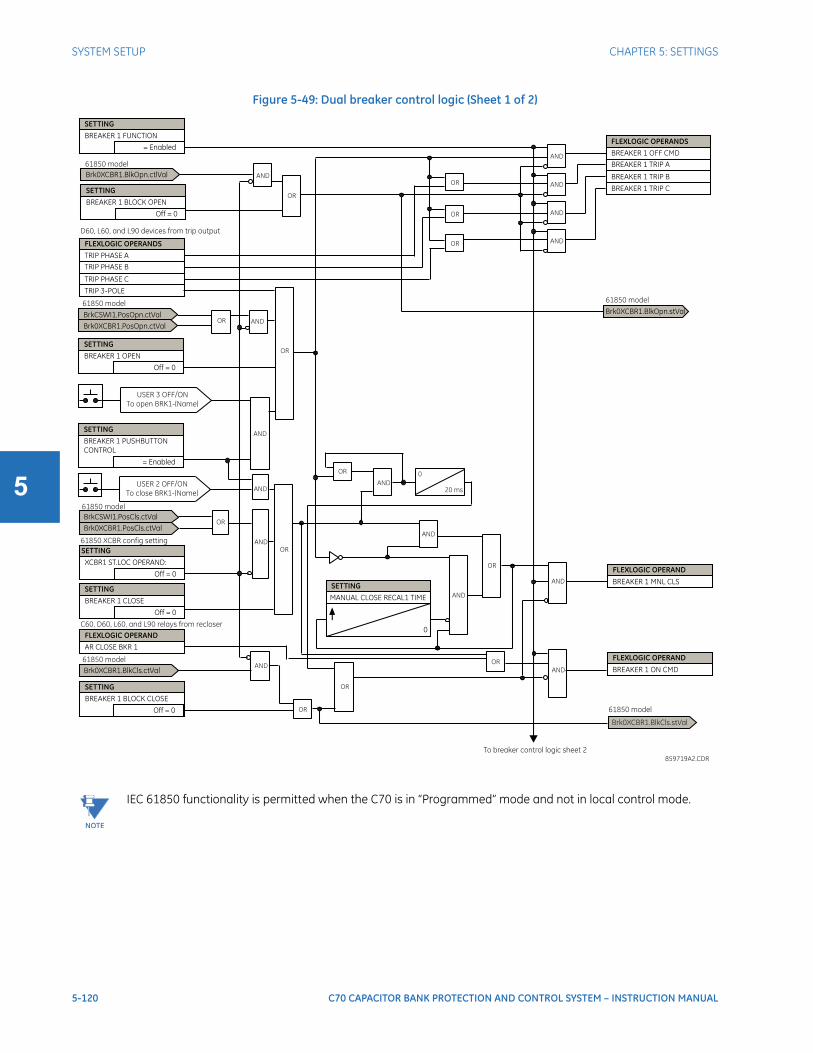
5-120 C70 CAPACITOR BANK PROTECTION AND CONTROL SYSTEM – INSTRUCTION MANUAL
SYSTEM SETUP CHAPTER 5: SETTINGS
5
Figure 5-49: Dual breaker control logic (Sheet 1 of 2)
NOTE
IEC 61850 functionality is permitted when the C70 is in “Programmed” mode and not in local control mode.

CHAPTER 5: SETTINGS SYSTEM SETUP
C70 CAPACITOR BANK PROTECTION AND CONTROL SYSTEM – INSTRUCTION MANUAL 5-121
5
Figure 5-50: Dual breaker control logic (Sheet 2 of 2)
The breaker element has direct hard-coded connections to the IEC 61850 model as shown in the logic diagram. This allows remote open/close operation of each breaker, using either CSWI or XCBR IEC 61850 logical nodes. IEC 61850 select-before-operate functionality, local/remote switch functionality, along with blocking of open/close commands are provided. Note that the dwell time for the IEC 61850 trip and close commands shown is one protection pass only. To maintain the close/open command for a certain time, do so on the contact outputs using the "Seal-in" setting, in the Trip Output element, or in FlexLogic.

5-122 C70 CAPACITOR BANK PROTECTION AND CONTROL SYSTEM – INSTRUCTION MANUAL
SYSTEM SETUP CHAPTER 5: SETTINGS
5
5.5.5 Disconnect switchesSETTINGS SYSTEM SETUP SWITCHES SWITCH 1(24)
The disconnect switch element contains the auxiliary logic for status and serves as the interface for opening and closing of disconnect switches from SCADA or through the front panel interface. The disconnect switch element can be used to create interlocking functionality. For greater security in determination of the switch pole position, both the 89/a and 89/b auxiliary contacts are used with reporting of the discrepancy between them. The number of available disconnect switches depends on the number of the CT/VT modules ordered with the C70.
SWITCH 1 FUNCTION — This setting enables and disables operation of the disconnect switch element.
SWITCH 1 NAME — Assign a user-defined name (up to six characters) to the disconnect switch. This name is used in flash messages related to disconnect switch 1.
SWITCH 1 MODE — This setting selects “3-Pole” mode, where disconnect switch poles have a single common auxiliary switch, or “1-Pole” mode where each disconnect switch pole has its own auxiliary switch.
SWITCH 1 OPEN — This setting selects an operand that creates a programmable signal to operate a contact output to open disconnect switch 1.
SWITCH 1 BLK OPEN — This setting selects an operand that prevents opening of the disconnect switch. This setting can be used for select-before-operate functionality or to block operation from a panel switch or from SCADA.
SWITCH 1 SWITCH 1
FUNCTION: DisabledRange: Disabled, Enabled
SWITCH 1 NAME:SW 1
Range: up to six alphanumeric characters
SWITCH 1 MODE:3-Pole
Range: 3-Pole, 1-Pole
SWITCH 1 OPEN:Off
Range: FlexLogic operand
SWITCH 1 BLK OPEN:Off
Range: FlexLogic operand
SWITCH 1 CLOSE:Off
Range: FlexLogic operand
SWITCH 1 BLK CLOSE:Off
Range: FlexLogic operand
SWTCH 1 ΦA/3P CLSD:Off
Range: FlexLogic operand
SWTCH 1 ΦA/3P OPND:Off
Range: FlexLogic operand
SWITCH 1 ΦB CLOSED:Off
Range: FlexLogic operand
SWITCH 1 ΦB OPENED:Off
Range: FlexLogic operand
SWITCH 1 ΦC CLOSED:Off
Range: FlexLogic operand
SWITCH 1 ΦC OPENED:Off
Range: FlexLogic operand
SWITCH 1 Toperate:0.070 s
Range: 0.000 to 65.535 s in steps of 0.001
SWITCH 1 ALARMDELAY: 0.000 s
Range: 0.000 to 65.535 s in steps of 0.001
SWITCH 1 EVENTS:Disabled
Range: Disabled, Enabled

CHAPTER 5: SETTINGS SYSTEM SETUP
C70 CAPACITOR BANK PROTECTION AND CONTROL SYSTEM – INSTRUCTION MANUAL 5-123
5
SWITCH 1 CLOSE — This setting selects an operand that creates a programmable signal to operate a contact output to close disconnect switch 1.
SWITCH 1 BLK CLOSE — This setting selects an operand that prevents closing of the disconnect switch. This setting can be used for select-before-operate functionality or to block operation from a panel switch or from SCADA.
SWTCH 1 ΦA/3P CLSD — This setting selects an operand, usually a contact input connected to a disconnect switch auxiliary position tracking mechanism. This input is a normally-open 89/a status input to create a logic 1 when the disconnect switch is closed. If the SWITCH 1 MODE setting is selected as “3-Pole,” this setting selects a single input as the operand used to track the disconnect switch open or closed position. If the mode is selected as “1-Pole,” the input mentioned is used to track phase A and the SWITCH 1 ΦB and SWITCH 1 ΦC settings select operands to track phases B and C, respectively.
SWTCH 1 ΦA/3P OPND — This setting selects an operand, usually a contact input, that is a normally-closed 89/b status input to create a logic 1 when the disconnect switch is open. If a separate 89/b contact input is not available, then an inverted 89/a status signal can be used.
SWITCH 1 ΦB CLOSED — If the mode is selected as three-pole, this setting has no function. If the mode is selected as single-pole, this input is used to track the disconnect switch phase B closed position as outlined for phase A.
SWITCH 1 ΦB OPENED — If the mode is selected as three-pole, this setting has no function. If the mode is selected as single-pole, this input is used to track the disconnect switch phase B opened position as outlined for phase A.
SWITCH 1 ΦC CLOSED — If the mode is selected as three-pole, this setting has no function. If the mode is selected as single-pole, this input is used to track the disconnect switch phase C closed position as outlined for phase A.
SWITCH 1 ΦC OPENED — If the mode is selected as three-pole, this setting has no function. If the mode is selected as single-pole, this input is used to track the disconnect switch phase C opened position as outlined for phase A.
SWITCH 1 Toperate — This setting specifies the required interval to overcome transient disagreement between the 89/a and 89/b auxiliary contacts during disconnect switch operation. If transient disagreement still exists after this time has expired, the SWITCH 1 BAD STATUS FlexLogic operand is asserted from alarm or blocking purposes.
SWITCH 1 ALARM DELAY — This setting specifies the delay interval during which a disagreement of status among the three-pole position tracking operands do not declare a pole disagreement. This allows for non-simultaneous operation of the poles.
NOTE
IEC 61850 functionality is permitted when the C70 is in “Programmed” mode and not in local control mode.
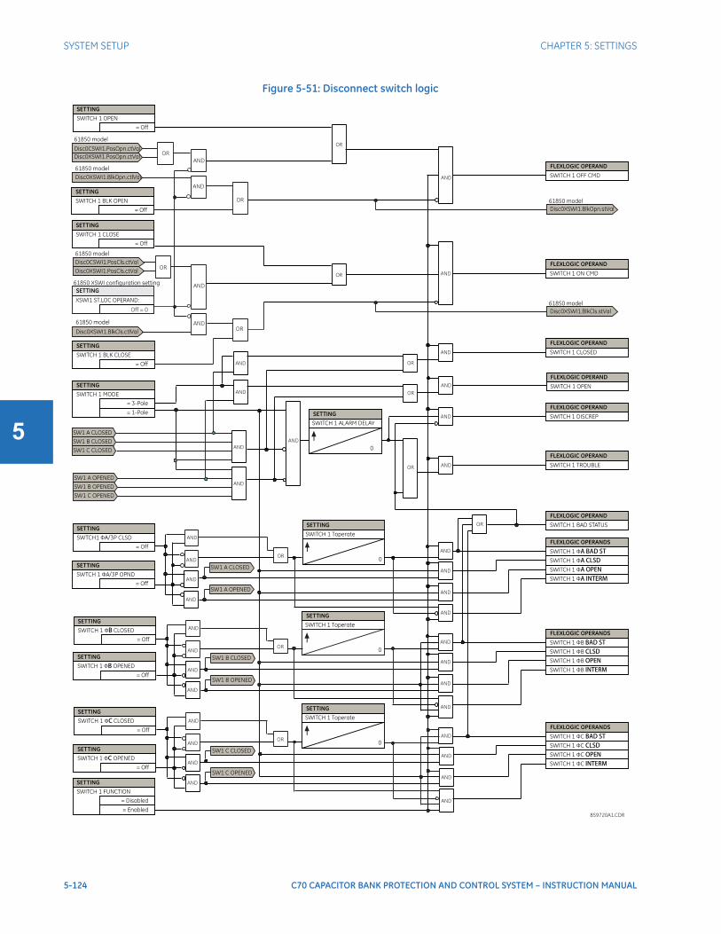
5-124 C70 CAPACITOR BANK PROTECTION AND CONTROL SYSTEM – INSTRUCTION MANUAL
SYSTEM SETUP CHAPTER 5: SETTINGS
5
Figure 5-51: Disconnect switch logic

CHAPTER 5: SETTINGS SYSTEM SETUP
C70 CAPACITOR BANK PROTECTION AND CONTROL SYSTEM – INSTRUCTION MANUAL 5-125
5
The switch element has direct hard-coded connections to the IEC 61850 model as shown in the logic diagram. This allows remote open/close operation of each switch, using either CSWI or XSWI IEC 61850 logical nodes. IEC 61850 select-before-operate functionality, local/remote switch functionality, along with blocking open/close commands are provided. Note that the dwell time for the IEC 61850 trip and close commands shown is one protection pass only. To maintain close/open command for a certain time, do so either on the contact outputs using the "Seal-in" setting or in FlexLogic.
5.5.6 FlexCurves
5.5.6.1 SettingsSETTINGS SYSTEM SETUP FLEXCURVES FLEXCURE A(D)
FlexCurves A through D have settings for entering times to reset and operate at the following pickup levels: 0.00 to 0.98 and 1.03 to 20.00. This data is converted into two continuous curves by linear interpolation between data points. To enter a custom FlexCurve, enter the reset and operate times (using the VALUE keys) for each selected pickup point (using the MESSAGE up/down keys) for the required protection curve (A, B, C, or D).
Table 5-15: FlexCurve table
FLEXCURVE A FLEXCURVE A TIME AT
0.00 xPKP: 0 msRange: 0 to 65535 ms in steps of 1
Reset Timems
Reset Timems
Operate Timems
Operate Timems
Operate Timems
Operate Timems
0.00 0.68 1.03 2.9 4.9 10.5
0.05 0.70 1.05 3.0 5.0 11.0
0.10 0.72 1.1 3.1 5.1 11.5
0.15 0.74 1.2 3.2 5.2 12.0
0.20 0.76 1.3 3.3 5.3 12.5
0.25 0.78 1.4 3.4 5.4 13.0
0.30 0.80 1.5 3.5 5.5 13.5
0.35 0.82 1.6 3.6 5.6 14.0
0.40 0.84 1.7 3.7 5.7 14.5
0.45 0.86 1.8 3.8 5.8 15.0
0.48 0.88 1.9 3.9 5.9 15.5
0.50 0.90 2.0 4.0 6.0 16.0
0.52 0.91 2.1 4.1 6.5 16.5
0.54 0.92 2.2 4.2 7.0 17.0
0.56 0.93 2.3 4.3 7.5 17.5
0.58 0.94 2.4 4.4 8.0 18.0
0.60 0.95 2.5 4.5 8.5 18.5
0.62 0.96 2.6 4.6 9.0 19.0
0.64 0.97 2.7 4.7 9.5 19.5
0.66 0.98 2.8 4.8 10.0 20.0
NOTE
The relay using a given FlexCurve applies linear approximation for times between the user-entered points. Take care when setting the two points that are close to the multiple of pickup of 1; that is, 0.98 pu and 1.03 pu. It is recommended to set the two times to a similar value, otherwise the linear approximation can result in undesired behavior for the operating quantity that is close to 1.00 pu.

5-126 C70 CAPACITOR BANK PROTECTION AND CONTROL SYSTEM – INSTRUCTION MANUAL
SYSTEM SETUP CHAPTER 5: SETTINGS
5
5.5.6.2 FlexCurve configuration with EnerVista softwareThe EnerVista software allows for easy configuration and management of FlexCurves and their associated data points. Prospective FlexCurves can be configured from a selection of standard curves to provide the best approximate fit , then specific data points can be edited afterwards. Alternately, curve data can be imported from a specified file (.csv format) by selecting the EnerVista Import Data From setting (Settings > System Setup > FlexCurves > FlexCurve).
Curves and data can be exported, viewed, and cleared by clicking the appropriate buttons. FlexCurves are customized by editing the operating time (ms) values at pre-defined per-unit current multiples. Note that the pickup multiples start at zero (implying the "reset time"), operating time below pickup, and operating time above pickup.
5.5.6.3 Recloser curve editingRecloser curve selection is special in that recloser curves can be shaped into a composite curve with a minimum response time and a fixed time above a specified pickup multiples. There are 41 recloser curve types supported. These definite operating times are useful to coordinate operating times, typically at higher currents and where upstream and downstream protective devices have different operating characteristics. The recloser curve configuration window shown here appears when the Initialize From setting in the EnerVista software is set to “Recloser Curve” and the Initialize FlexCurve button is clicked.
Figure 5-52: Recloser curve initialization
5.5.6.4 ExampleA composite curve can be created from the GE_111 standard with MRT = 200 ms and HCT initially disabled and then enabled at eight times pickup with an operating time of 30 ms. At approximately four times pickup, the curve operating time is equal to the MRT and from then onwards the operating time remains at 200 ms.
NOTE
The Multiplier and Adder settings only affect the curve portion of the characteristic and not the MRT and HCT settings. The HCT settings override the MRT settings for multiples of pickup greater than the HCT ratio.
842721A1.CDR
Multiplier: Scales (multiplies) the curve operating times
Addr: Adds the time specified in this field (in ms) to eachoperating time value.curve
Minimum Response Time (MRT): If enabled, the MRT settingdefines the shortest operating time even if the curve suggestsa shorter time at higher current multiples. A composite operatingcharacteristic is effectively defined. For current multiples lowerthan the intersection point, the curve dictates the operating time;otherwise, the MRT does. An information message appearswhen attempting to apply an MRT shorter than the minimumcurve time.
High Current Time:
HCT Ratio
HCT
Allows the user to set a pickup multiplefrom which point onwards the operating time is fixed. This isnormally only required at higher current levels. Thedefines the high current pickup multiple; the defines theoperating time.

CHAPTER 5: SETTINGS SYSTEM SETUP
C70 CAPACITOR BANK PROTECTION AND CONTROL SYSTEM – INSTRUCTION MANUAL 5-127
5
Figure 5-53: Composite recloser curve with HCT disabled
With the HCT feature enabled, the operating time reduces to 30 ms for pickup multiples exceeding eight times pickup.
Figure 5-54: Composite recloser curve with HCT enabled
5.5.6.5 Standard recloser curvesThe following graphs display standard recloser curves available for the C70.
NOTE
Configuring a composite curve with an increase in operating time at increased pickup multiples is not allowed. If this is attempted, the EnerVista software generates an error message and discards the proposed changes.
842719A1.CDR
842720A1.CDR

5-128 C70 CAPACITOR BANK PROTECTION AND CONTROL SYSTEM – INSTRUCTION MANUAL
SYSTEM SETUP CHAPTER 5: SETTINGS
5
Figure 5-55: Recloser curves GE101 to GE106
Figure 5-56: Recloser curves GE113, GE120, GE138, and GE142
GE104
1 1.2 1.5 2 2.5 3 4 5 6 7 8 9 10 12 15 20
0.01
0.02
0.05
0.1
0.2
0.5
1
2
CURRENT (multiple of pickup)
TIM
E (s
ec)
GE101 GE102
GE103
GE106
GE105
842723A1.CDR
1 1.2 1.5 2 2.5 3 4 5 6 7 8 9 10 12 15 200.05
0.1
0.2
0.5
1
2
5
10
20
50
CURRENT (multiple of pickup)
TIM
E (s
ec)
GE113
GE142
GE138
GE120
842725A1.CDR

CHAPTER 5: SETTINGS SYSTEM SETUP
C70 CAPACITOR BANK PROTECTION AND CONTROL SYSTEM – INSTRUCTION MANUAL 5-129
5
Figure 5-57: Recloser curves GE134, GE137, GE140, GE151, and GE201
Figure 5-58: Recloser curves GE131, GE141, GE152, and GE200
1 1.2 1.5 2 2.5 3 4 5 6 7 8 9 10 12 15 20
0.5
1
2
5
10
20
50
CURRENT (multiple of pickup)
TIM
E (s
ec)
GE134
GE151
GE140
GE137
GE201
842730A1.CDR
1 1.2 1.5 2 2.5 3 4 5 6 7 8 9 10 12 15 202
5
10
20
50
CURRENT (multiple of pickup)
TIM
E (s
ec)
GE131
GE200
GE152
GE141
842728A1.CDR

5-130 C70 CAPACITOR BANK PROTECTION AND CONTROL SYSTEM – INSTRUCTION MANUAL
SYSTEM SETUP CHAPTER 5: SETTINGS
5
Figure 5-59: Recloser curves GE133, GE161, GE162, GE163, GE164, and GE165
Figure 5-60: Recloser curves GE116, GE117, GE118, GE132, GE136, and GE139
842729A1.CDR
1 1.2 1.5 2 2.5 3 4 5 6 7 8 9 10 12 15 200.01
0.02
0.05
0.1
0.2
0.5
1
2
5
10
20
50
CURRENT (multiple of pickup)
TIM
E (s
ec)
GE133
GE163
GE162
GE161
GE165
GE164
842726A1.CDR
1 1.2 1.5 2 2.5 3 4 5 6 7 8 9 10 12 15 200.01
0.02
0.05
0.1
0.2
0.5
1
2
5
10
20
CURRENT (multiple of pickup)
TIM
E (s
ec)
GE116
GE132
GE118 GE117
GE139
GE136

CHAPTER 5: SETTINGS SYSTEM SETUP
C70 CAPACITOR BANK PROTECTION AND CONTROL SYSTEM – INSTRUCTION MANUAL 5-131
5
Figure 5-61: Recloser curves GE107, GE111, GE112, GE114, GE115, GE121, and GE122
Figure 5-62: Recloser curves GE119, GE135, and GE202
842724A1.CDR
1 1.2 1.5 2 2.5 3 4 5 6 7 8 9 10 12 15 200.01
0.02
0.05
0.1
0.2
0.5
1
2
5
10
20
CURRENT (multiple of pickup)
TIM
E (s
ec)
GE121
GE114
GE112
GE122
GE107 GE115
GE111
842727A1.CDR
1 1.2 1.5 2 2.5 3 4 5 6 7 8 9 10 12 15 200.2
0.5
1
2
5
10
20
50
CURRENT (multiple of pickup)
TIM
E (s
ec)
GE119
GE202
GE135

5-132 C70 CAPACITOR BANK PROTECTION AND CONTROL SYSTEM – INSTRUCTION MANUAL
FLEXLOGIC CHAPTER 5: SETTINGS
5
5.6 FlexLogic
5.6.1 FlexLogic operandsFor flexibility, the arrangement of internal digital logic combines fixed and user-programmed parameters. Logic upon which individual features are designed is fixed, and all other logic, from contact input signals through elements or combinations of elements to contact outputs, is variable. The user has complete control of all variable logic through FlexLogic. In general, the system receives analog and digital inputs that it uses to produce analog and digital outputs. The figure shows major subsystems of a generic UR-series relay involved in this process.
Figure 5-63: UR architecture overview
The states of all digital signals used in the C70 are represented by flags (or FlexLogic operands, which are described later in this section). A digital “1” is represented by a set flag. Any external contact change-of-state can be used to block an element from operating, as an input to a control feature in a FlexLogic equation, or to operate a contact output. The state of the contact input can be displayed locally or viewed remotely via the communications facilities provided. If a simple scheme where a contact input is used to block an element is wanted, this selection is made when programming the element. This capability also applies to the other features that set flags: elements, virtual inputs, remote inputs, schemes, and human operators.
If more complex logic than shown in the figure is required, it is implemented via FlexLogic. For example, to have the closed state of contact input H7a and the operated state of the phase undervoltage element block the operation of the phase time overcurrent element, the two control input states are programmed in a FlexLogic equation. This equation ANDs the two control inputs to produce a virtual output that is then selected when programming the phase time overcurrent to be used as a blocking input. Virtual outputs can only be created by FlexLogic equations.
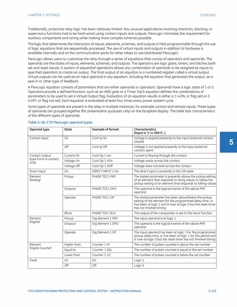
CHAPTER 5: SETTINGS FLEXLOGIC
C70 CAPACITOR BANK PROTECTION AND CONTROL SYSTEM – INSTRUCTION MANUAL 5-133
5
Traditionally, protective relay logic has been relatively limited. Any unusual applications involving interlocks, blocking, or supervisory functions had to be hard-wired using contact inputs and outputs. FlexLogic minimizes the requirement for auxiliary components and wiring while making more complex schemes possible.
The logic that determines the interaction of inputs, elements, schemes, and outputs is field-programmable through the use of logic equations that are sequentially processed. The use of virtual inputs and outputs in addition to hardware is available internally and on the communication ports for other relays to use (distributed FlexLogic).
FlexLogic allows users to customize the relay through a series of equations that consist of operators and operands. The operands are the states of inputs, elements, schemes, and outputs. The operators are logic gates, timers, and latches (with set and reset inputs). A system of sequential operations allows any combination of operands to be assigned as inputs to specified operators to create an output. The final output of an equation is a numbered register called a virtual output. Virtual outputs can be used as an input operand in any equation, including the equation that generates the output, as a seal-in or other type of feedback.
A FlexLogic equation consists of parameters that are either operands or operators. Operands have a logic state of 1 or 0. Operators provide a defined function, such as an AND gate or a Timer. Each equation defines the combinations of parameters to be used to set a Virtual Output flag. Evaluation of an equation results in either a 1 (=ON, or flag set) or 0 (=OFF, or flag not set). Each equation is evaluated at least four times every power system cycle.
Some types of operands are present in the relay in multiple instances, for example contact and remote inputs. These types of operands are grouped together (for presentation purposes only) on the faceplate display. The table lists characteristics of the different types of operands.
Table 5-16: C70 FlexLogic operand types
Operand type State Example of format Characteristics[Input Is ‘1’ (= ON) if...]
Contact Input On Cont Ip On Voltage is applied presently to the input (external contact closed)
Off Cont Ip Off Voltage is not applied presently to the input (external contact open)
Contact Output(type Form-A contact only)
Current On Cont Op 1 Ion Current is flowing through the contact
Voltage On Cont Op 1 VOn Voltage exists across the contact
Voltage Off Cont Op 1 VOff Voltage does not exist across the contact
Direct Input On DIRECT INPUT 1 On The direct input is presently in the ON state
Element(Analog)
Pickup PHASE TOC1 PKP The tested parameter is presently above the pickup setting of an element that responds to rising values or below the pickup setting of an element that responds to falling values
Dropout PHASE TOC1 DPO This operand is the logical inverse of the above PKP operand
Operate PHASE TOC1 OP The tested parameter has been above/below the pickup setting of the element for the programmed delay time, or has been at logic 1 and is now at logic 0 but the reset timer has not finished timing
Block PHASE TOC1 BLK The output of the comparator is set to the block function
Element(Digital)
Pickup Dig Element 1 PKP The input operand is at logic 1
Dropout Dig Element 1 DPO This operand is the logical inverse of the above PKP operand
Operate Dig Element 1 OP The input operand has been at logic 1 for the programmed pickup delay time, or has been at logic 1 for this period and is now at logic 0 but the reset timer has not finished timing
Element(Digital Counter)
Higher than Counter 1 HI The number of pulses counted is above the set number
Equal to Counter 1 EQL The number of pulses counted is equal to the set number
Lower than Counter 1 LO The number of pulses counted is below the set number
Fixed On On Logic 1
Off Off Logic 0

5-134 C70 CAPACITOR BANK PROTECTION AND CONTROL SYSTEM – INSTRUCTION MANUAL
FLEXLOGIC CHAPTER 5: SETTINGS
5
The following table lists alphabetically the operands available for the relay.
Table 5-17: C70 FlexLogic operands
RxGOOSE Boolean On RxGOOSE Boolean 1 On The RxGOOSE Boolean is presently in the ON state
Virtual Input On Virt Ip 1 On The virtual input is presently in the ON state
Virtual Output On Virt Op 1 On The virtual output is presently in the set state (that is, evaluation of the equation that produces this virtual output results in a "1")
Operand type Operand syntax Operand description
CONTROL PUSHBUTTONS
CONTROL PUSHBTN 1 ONCONTROL PUSHBTN 2 ONCONTROL PUSHBTN 3 ONCONTROL PUSHBTN 4 ONCONTROL PUSHBTN 5 ONCONTROL PUSHBTN 6 ONCONTROL PUSHBTN 7 ON
Control pushbutton 1 is being pressedControl pushbutton 2 is being pressedControl pushbutton 3 is being pressedControl pushbutton 4 is being pressedControl pushbutton 5 is being pressedControl pushbutton 6 is being pressedControl pushbutton 7 is being pressed
CYBERSENTRY ROLE ADMIN ACTROLE SUPERVISOR ACTROLE ENGINEER ACTROLE OPERATOR ACTROLE OBSERVER ACTROLE EXTERNAL ACTAUTHENTICATION FAILUNAUTH FW ATTEMPTUNAUTH SETTING WRITERADIUS SRV UNAVAILABLEACCT SRV UNAVAILABLE
Administrator role is active and is set to true when that is the caseSupervisor role is active and is set to true when that is the caseEngineer role is active and is set to true when that is the caseOperator role is active and is set to true when that is the caseObserver role is active and is set to true when that is the caseExternal role is active and is set to true when that is the caseOperand set for Failed Authentication self-test and alarmOperand set for firmware lock self-test and alarmOperand set for settings lock self-test and alarmOperand set for RADIUS servers unavailable self-testOperand set for ACCOUNTING servers unavailable self-test
DIRECT DEVICES DIRECT DEVICE 1On↓
DIRECT DEVICE 16OnDIRECT DEVICE 1Off
↓DIRECT DEVICE 16Off
Flag is set, logic=1↓
Flag is set, logic=1Flag is set, logic=1
↓Flag is set, logic=1
DIRECT INPUT/OUTPUT CHANNEL MONITORING
DIR IO CH1 CRC ALARM
DIR IO CH2 CRC ALARM
DIR IO CH1 UNRET ALM
DIR IO CH2 UNRET ALM
The rate of direct input messages received on channel 1 and failing the CRC exceeded the user-specified levelThe rate of direct input messages received on channel 2 and failing the CRC exceeded the user-specified levelThe rate of returned direct input/output messages on channel 1 exceeded the user-specified level (ring configurations only)The rate of returned direct input/output messages on channel 2 exceeded the user-specified level (ring configurations only)
ELEMENT:Auxiliary overvoltage
AUX OV1 PKPAUX OV1 DPOAUX OV1 OP
Auxiliary overvoltage element has picked upAuxiliary overvoltage element has dropped outAuxiliary overvoltage element has operated
AUX OV2 to 3 Same set of operands as shown for AUX OV1
ELEMENT: Automatic voltage regulator
AVR 1 CLOSE PKPAVR 1 CLOSE OPAVR 1 CLOSE DPOAVR 1 OPEN PKPAVR 1 OPEN OPAVR 1 OPEN DPO
Automatic voltage regulator 1 picked up; close command pendingAutomatic voltage regulator 1 issued a close commandClose command of automatic voltage regulator 1 dropped outAutomatic voltage regulator 1 picked up; open command pendingAutomatic voltage regulator 1 issued an open commandOpen command of automatic voltage regulator 1 dropped out
AVR 2 to 3 Same set of operands as shown for AVR 1
Operand type State Example of format Characteristics[Input Is ‘1’ (= ON) if...]
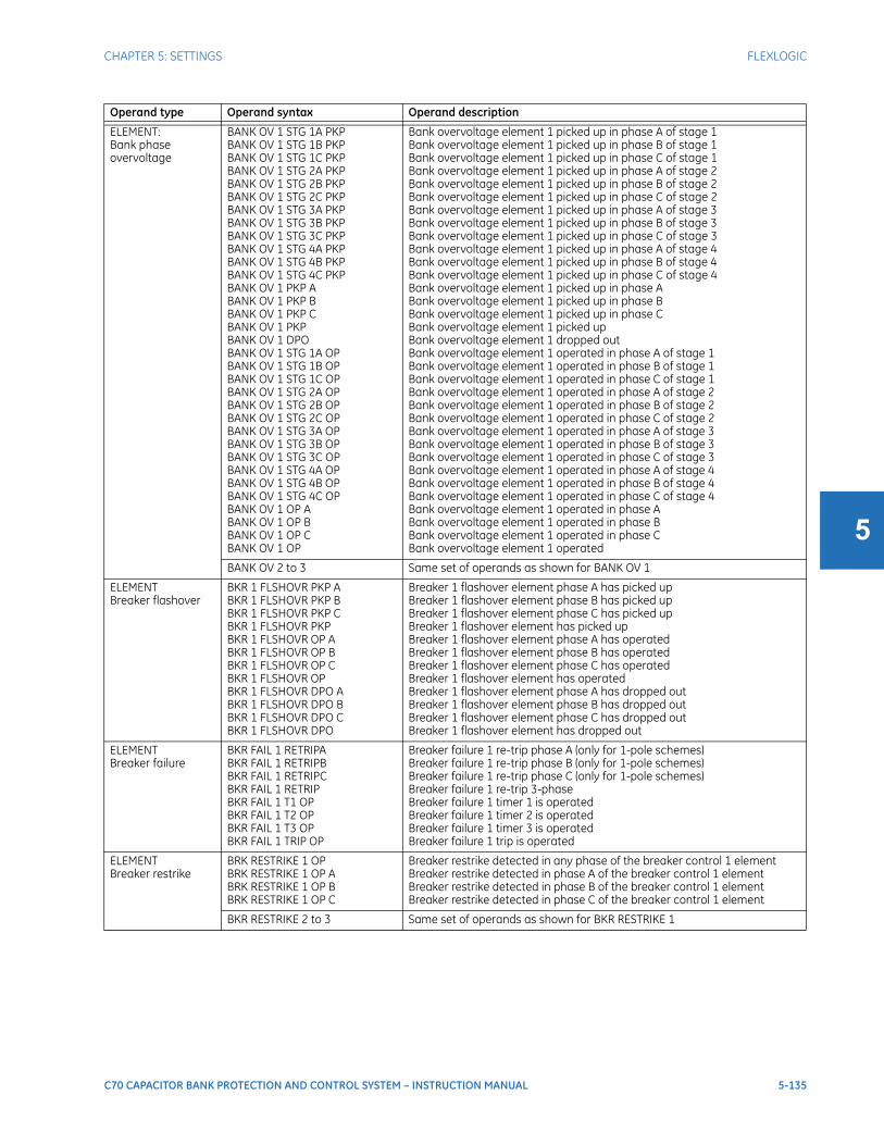
CHAPTER 5: SETTINGS FLEXLOGIC
C70 CAPACITOR BANK PROTECTION AND CONTROL SYSTEM – INSTRUCTION MANUAL 5-135
5
ELEMENT:Bank phase overvoltage
BANK OV 1 STG 1A PKPBANK OV 1 STG 1B PKPBANK OV 1 STG 1C PKPBANK OV 1 STG 2A PKPBANK OV 1 STG 2B PKPBANK OV 1 STG 2C PKPBANK OV 1 STG 3A PKPBANK OV 1 STG 3B PKPBANK OV 1 STG 3C PKPBANK OV 1 STG 4A PKPBANK OV 1 STG 4B PKPBANK OV 1 STG 4C PKPBANK OV 1 PKP ABANK OV 1 PKP BBANK OV 1 PKP CBANK OV 1 PKPBANK OV 1 DPOBANK OV 1 STG 1A OPBANK OV 1 STG 1B OPBANK OV 1 STG 1C OPBANK OV 1 STG 2A OPBANK OV 1 STG 2B OPBANK OV 1 STG 2C OPBANK OV 1 STG 3A OPBANK OV 1 STG 3B OPBANK OV 1 STG 3C OPBANK OV 1 STG 4A OPBANK OV 1 STG 4B OPBANK OV 1 STG 4C OPBANK OV 1 OP ABANK OV 1 OP BBANK OV 1 OP CBANK OV 1 OP
Bank overvoltage element 1 picked up in phase A of stage 1Bank overvoltage element 1 picked up in phase B of stage 1Bank overvoltage element 1 picked up in phase C of stage 1Bank overvoltage element 1 picked up in phase A of stage 2Bank overvoltage element 1 picked up in phase B of stage 2Bank overvoltage element 1 picked up in phase C of stage 2Bank overvoltage element 1 picked up in phase A of stage 3Bank overvoltage element 1 picked up in phase B of stage 3Bank overvoltage element 1 picked up in phase C of stage 3Bank overvoltage element 1 picked up in phase A of stage 4Bank overvoltage element 1 picked up in phase B of stage 4Bank overvoltage element 1 picked up in phase C of stage 4Bank overvoltage element 1 picked up in phase ABank overvoltage element 1 picked up in phase BBank overvoltage element 1 picked up in phase CBank overvoltage element 1 picked upBank overvoltage element 1 dropped outBank overvoltage element 1 operated in phase A of stage 1Bank overvoltage element 1 operated in phase B of stage 1Bank overvoltage element 1 operated in phase C of stage 1Bank overvoltage element 1 operated in phase A of stage 2Bank overvoltage element 1 operated in phase B of stage 2Bank overvoltage element 1 operated in phase C of stage 2Bank overvoltage element 1 operated in phase A of stage 3Bank overvoltage element 1 operated in phase B of stage 3Bank overvoltage element 1 operated in phase C of stage 3Bank overvoltage element 1 operated in phase A of stage 4Bank overvoltage element 1 operated in phase B of stage 4Bank overvoltage element 1 operated in phase C of stage 4Bank overvoltage element 1 operated in phase ABank overvoltage element 1 operated in phase BBank overvoltage element 1 operated in phase CBank overvoltage element 1 operated
BANK OV 2 to 3 Same set of operands as shown for BANK OV 1
ELEMENTBreaker flashover
BKR 1 FLSHOVR PKP ABKR 1 FLSHOVR PKP BBKR 1 FLSHOVR PKP CBKR 1 FLSHOVR PKPBKR 1 FLSHOVR OP ABKR 1 FLSHOVR OP BBKR 1 FLSHOVR OP CBKR 1 FLSHOVR OPBKR 1 FLSHOVR DPO ABKR 1 FLSHOVR DPO BBKR 1 FLSHOVR DPO CBKR 1 FLSHOVR DPO
Breaker 1 flashover element phase A has picked upBreaker 1 flashover element phase B has picked upBreaker 1 flashover element phase C has picked upBreaker 1 flashover element has picked upBreaker 1 flashover element phase A has operatedBreaker 1 flashover element phase B has operatedBreaker 1 flashover element phase C has operatedBreaker 1 flashover element has operatedBreaker 1 flashover element phase A has dropped outBreaker 1 flashover element phase B has dropped outBreaker 1 flashover element phase C has dropped outBreaker 1 flashover element has dropped out
ELEMENTBreaker failure
BKR FAIL 1 RETRIPABKR FAIL 1 RETRIPBBKR FAIL 1 RETRIPCBKR FAIL 1 RETRIPBKR FAIL 1 T1 OPBKR FAIL 1 T2 OPBKR FAIL 1 T3 OPBKR FAIL 1 TRIP OP
Breaker failure 1 re-trip phase A (only for 1-pole schemes)Breaker failure 1 re-trip phase B (only for 1-pole schemes)Breaker failure 1 re-trip phase C (only for 1-pole schemes)Breaker failure 1 re-trip 3-phaseBreaker failure 1 timer 1 is operatedBreaker failure 1 timer 2 is operatedBreaker failure 1 timer 3 is operatedBreaker failure 1 trip is operated
ELEMENTBreaker restrike
BRK RESTRIKE 1 OPBRK RESTRIKE 1 OP ABRK RESTRIKE 1 OP BBRK RESTRIKE 1 OP C
Breaker restrike detected in any phase of the breaker control 1 elementBreaker restrike detected in phase A of the breaker control 1 elementBreaker restrike detected in phase B of the breaker control 1 elementBreaker restrike detected in phase C of the breaker control 1 element
BKR RESTRIKE 2 to 3 Same set of operands as shown for BKR RESTRIKE 1
Operand type Operand syntax Operand description
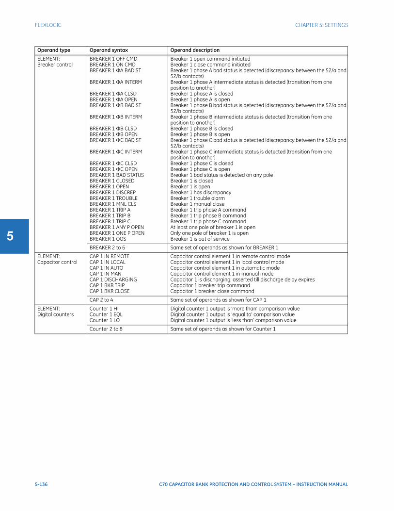
5-136 C70 CAPACITOR BANK PROTECTION AND CONTROL SYSTEM – INSTRUCTION MANUAL
FLEXLOGIC CHAPTER 5: SETTINGS
5
ELEMENT:Breaker control
BREAKER 1 OFF CMDBREAKER 1 ON CMDBREAKER 1 ΦA BAD ST
BREAKER 1 ΦA INTERM
BREAKER 1 ΦA CLSDBREAKER 1 ΦA OPENBREAKER 1 ΦB BAD ST
BREAKER 1 ΦB INTERM
BREAKER 1 ΦB CLSDBREAKER 1 ΦB OPENBREAKER 1 ΦC BAD ST
BREAKER 1 ΦC INTERM
BREAKER 1 ΦC CLSDBREAKER 1 ΦC OPENBREAKER 1 BAD STATUSBREAKER 1 CLOSEDBREAKER 1 OPENBREAKER 1 DISCREPBREAKER 1 TROUBLEBREAKER 1 MNL CLSBREAKER 1 TRIP ABREAKER 1 TRIP BBREAKER 1 TRIP CBREAKER 1 ANY P OPENBREAKER 1 ONE P OPENBREAKER 1 OOS
Breaker 1 open command initiatedBreaker 1 close command initiatedBreaker 1 phase A bad status is detected (discrepancy between the 52/a and 52/b contacts)Breaker 1 phase A intermediate status is detected (transition from one position to another)Breaker 1 phase A is closedBreaker 1 phase A is openBreaker 1 phase B bad status is detected (discrepancy between the 52/a and 52/b contacts)Breaker 1 phase B intermediate status is detected (transition from one position to another)Breaker 1 phase B is closedBreaker 1 phase B is openBreaker 1 phase C bad status is detected (discrepancy between the 52/a and 52/b contacts)Breaker 1 phase C intermediate status is detected (transition from one position to another)Breaker 1 phase C is closedBreaker 1 phase C is openBreaker 1 bad status is detected on any poleBreaker 1 is closedBreaker 1 is openBreaker 1 has discrepancyBreaker 1 trouble alarmBreaker 1 manual closeBreaker 1 trip phase A commandBreaker 1 trip phase B commandBreaker 1 trip phase C commandAt least one pole of breaker 1 is openOnly one pole of breaker 1 is openBreaker 1 is out of service
BREAKER 2 to 6 Same set of operands as shown for BREAKER 1
ELEMENT:Capacitor control
CAP 1 IN REMOTECAP 1 IN LOCALCAP 1 IN AUTOCAP 1 IN MANCAP 1 DISCHARGINGCAP 1 BKR TRIPCAP 1 BKR CLOSE
Capacitor control element 1 in remote control modeCapacitor control element 1 in local control modeCapacitor control element 1 in automatic modeCapacitor control element 1 in manual modeCapacitor 1 is discharging; asserted till discharge delay expiresCapacitor 1 breaker trip commandCapacitor 1 breaker close command
CAP 2 to 4 Same set of operands as shown for CAP 1
ELEMENT:Digital counters
Counter 1 HICounter 1 EQLCounter 1 LO
Digital counter 1 output is ‘more than’ comparison valueDigital counter 1 output is ‘equal to’ comparison valueDigital counter 1 output is ‘less than’ comparison value
Counter 2 to 8 Same set of operands as shown for Counter 1
Operand type Operand syntax Operand description
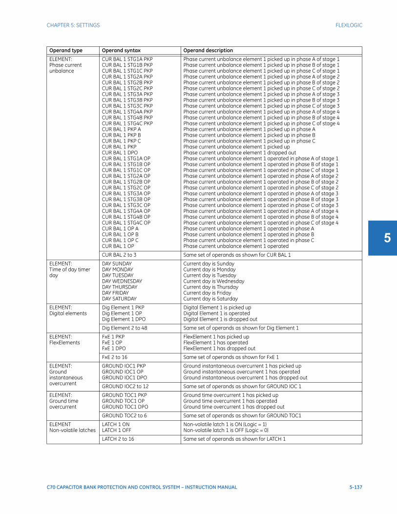
CHAPTER 5: SETTINGS FLEXLOGIC
C70 CAPACITOR BANK PROTECTION AND CONTROL SYSTEM – INSTRUCTION MANUAL 5-137
5
ELEMENT:Phase current unbalance
CUR BAL 1 STG1A PKPCUR BAL 1 STG1B PKPCUR BAL 1 STG1C PKPCUR BAL 1 STG2A PKPCUR BAL 1 STG2B PKPCUR BAL 1 STG2C PKPCUR BAL 1 STG3A PKPCUR BAL 1 STG3B PKPCUR BAL 1 STG3C PKPCUR BAL 1 STG4A PKPCUR BAL 1 STG4B PKPCUR BAL 1 STG4C PKPCUR BAL 1 PKP ACUR BAL 1 PKP BCUR BAL 1 PKP CCUR BAL 1 PKPCUR BAL 1 DPOCUR BAL 1 STG1A OPCUR BAL 1 STG1B OPCUR BAL 1 STG1C OPCUR BAL 1 STG2A OPCUR BAL 1 STG2B OPCUR BAL 1 STG2C OPCUR BAL 1 STG3A OPCUR BAL 1 STG3B OPCUR BAL 1 STG3C OPCUR BAL 1 STG4A OPCUR BAL 1 STG4B OPCUR BAL 1 STG4C OPCUR BAL 1 OP ACUR BAL 1 OP BCUR BAL 1 OP CCUR BAL 1 OP
Phase current unbalance element 1 picked up in phase A of stage 1Phase current unbalance element 1 picked up in phase B of stage 1Phase current unbalance element 1 picked up in phase C of stage 1Phase current unbalance element 1 picked up in phase A of stage 2Phase current unbalance element 1 picked up in phase B of stage 2Phase current unbalance element 1 picked up in phase C of stage 2Phase current unbalance element 1 picked up in phase A of stage 3Phase current unbalance element 1 picked up in phase B of stage 3Phase current unbalance element 1 picked up in phase C of stage 3Phase current unbalance element 1 picked up in phase A of stage 4Phase current unbalance element 1 picked up in phase B of stage 4Phase current unbalance element 1 picked up in phase C of stage 4Phase current unbalance element 1 picked up in phase APhase current unbalance element 1 picked up in phase BPhase current unbalance element 1 picked up in phase CPhase current unbalance element 1 picked upPhase current unbalance element 1 dropped outPhase current unbalance element 1 operated in phase A of stage 1Phase current unbalance element 1 operated in phase B of stage 1Phase current unbalance element 1 operated in phase C of stage 1Phase current unbalance element 1 operated in phase A of stage 2Phase current unbalance element 1 operated in phase B of stage 2Phase current unbalance element 1 operated in phase C of stage 2Phase current unbalance element 1 operated in phase A of stage 3Phase current unbalance element 1 operated in phase B of stage 3Phase current unbalance element 1 operated in phase C of stage 3Phase current unbalance element 1 operated in phase A of stage 4Phase current unbalance element 1 operated in phase B of stage 4Phase current unbalance element 1 operated in phase C of stage 4Phase current unbalance element 1 operated in phase APhase current unbalance element 1 operated in phase BPhase current unbalance element 1 operated in phase CPhase current unbalance element 1 operated
CUR BAL 2 to 3 Same set of operands as shown for CUR BAL 1
ELEMENT:Time of day timer day
DAY SUNDAYDAY MONDAYDAY TUESDAYDAY WEDNESDAYDAY THURSDAYDAY FRIDAYDAY SATURDAY
Current day is SundayCurrent day is MondayCurrent day is TuesdayCurrent day is WednesdayCurrent day is ThursdayCurrent day is FridayCurrent day is Saturday
ELEMENT:Digital elements
Dig Element 1 PKPDig Element 1 OPDig Element 1 DPO
Digital Element 1 is picked upDigital Element 1 is operatedDigital Element 1 is dropped out
Dig Element 2 to 48 Same set of operands as shown for Dig Element 1
ELEMENT:FlexElements
FxE 1 PKPFxE 1 OPFxE 1 DPO
FlexElement 1 has picked upFlexElement 1 has operatedFlexElement 1 has dropped out
FxE 2 to 16 Same set of operands as shown for FxE 1
ELEMENT:Ground instantaneous overcurrent
GROUND IOC1 PKPGROUND IOC1 OPGROUND IOC1 DPO
Ground instantaneous overcurrent 1 has picked upGround instantaneous overcurrent 1 has operatedGround instantaneous overcurrent 1 has dropped out
GROUND IOC2 to 12 Same set of operands as shown for GROUND IOC 1
ELEMENT:Ground time overcurrent
GROUND TOC1 PKPGROUND TOC1 OPGROUND TOC1 DPO
Ground time overcurrent 1 has picked upGround time overcurrent 1 has operatedGround time overcurrent 1 has dropped out
GROUND TOC2 to 6 Same set of operands as shown for GROUND TOC1
ELEMENTNon-volatile latches
LATCH 1 ONLATCH 1 OFF
Non-volatile latch 1 is ON (Logic = 1)Non-volatile latch 1 is OFF (Logic = 0)
LATCH 2 to 16 Same set of operands as shown for LATCH 1
Operand type Operand syntax Operand description

5-138 C70 CAPACITOR BANK PROTECTION AND CONTROL SYSTEM – INSTRUCTION MANUAL
FLEXLOGIC CHAPTER 5: SETTINGS
5
ELEMENT:Time of day timer month
MONTH JANUARYMONTH FEBRUARYMONTH MARCHMONTH APRILMONTH MAYMONTH JUNEMONTH JULYMONTH AUGUSTMONTH SEPTEMBERMONTH OCTOBERMONTH NOVEMBERMONTH DECEMBER
Current month is JanuaryCurrent month is FebruaryCurrent month is MarchCurrent month is AprilCurrent month is MayCurrent month is JuneCurrent month is JulyCurrent month is AugustCurrent month is SeptemberCurrent month is OctoberCurrent month is NovemberCurrent month is December
ELEMENT:Negative-sequence directional overcurrent
NEG SEQ DIR OC1 FWDNEG SEQ DIR OC1 REVNEG SEQ DIR OC2 FWDNEG SEQ DIR OC2 REV
Negative-sequence directional overcurrent 1 forward has operatedNegative-sequence directional overcurrent 1 reverse has operatedNegative-sequence directional overcurrent 2 forward has operatedNegative-sequence directional overcurrent 2 reverse has operated
ELEMENT:Negative-sequence instantaneous overcurrent
NEG SEQ IOC1 PKPNEG SEQ IOC1 OPNEG SEQ IOC1 DPO
Negative-sequence instantaneous overcurrent 1 has picked upNegative-sequence instantaneous overcurrent 1 has operatedNegative-sequence instantaneous overcurrent 1 has dropped out
NEG SEQ IOC2 Same set of operands as shown for NEG SEQ IOC1
ELEMENT:Negative-sequence overvoltage
NEG SEQ OV1 PKPNEG SEQ OV1 DPONEG SEQ OV1 OP
Negative-sequence overvoltage element has picked upNegative-sequence overvoltage element has dropped outNegative-sequence overvoltage element has operated
NEG SEQ OV2 to 3 Same set of operands as shown for NEG SEQ OV1
ELEMENT:Negative-sequence time overcurrent
NEG SEQ TOC1 PKPNEG SEQ TOC1 OPNEG SEQ TOC1 DPO
Negative-sequence time overcurrent 1 has picked upNegative-sequence time overcurrent 1 has operatedNegative-sequence time overcurrent 1 has dropped out
NEG SEQ TOC2 Same set of operands as shown for NEG SEQ TOC1
ELEMENT:Neutral instantaneous overcurrent
NEUTRAL IOC1 PKPNEUTRAL IOC1 OPNEUTRAL IOC1 DPO
Neutral instantaneous overcurrent 1 has picked upNeutral instantaneous overcurrent 1 has operatedNeutral instantaneous overcurrent 1 has dropped out
NEUTRAL IOC2 to 12 Same set of operands as shown for NEUTRAL IOC1
ELEMENT:Neutral overvoltage
NEUTRAL OV1 PKPNEUTRAL OV1 DPONEUTRAL OV1 OP
Neutral overvoltage element 1 has picked upNeutral overvoltage element 1 has dropped outNeutral overvoltage element 1 has operated
NEUTRAL OV2 to 3 Same set of operands as shown for NEUTRAL OV1
ELEMENT:Neutral time overcurrent
NEUTRAL TOC1 PKPNEUTRAL TOC1 OPNEUTRAL TOC1 DPO
Neutral time overcurrent 1 has picked upNeutral time overcurrent 1 has operatedNeutral time overcurrent 1 has dropped out
NEUTRAL TOC2 to 6 Same set of operands as shown for NEUTRAL TOC1
ELEMENT:Neutral current unbalance
NTRL CUR 1 STG1 PKPNTRL CUR 1 STG2 PKPNTRL CUR 1 STG3 PKPNTRL CUR 1 STG4 PKPNTRL CUR 1 PKPNTRL CUR 1 DPONTRL CUR 1 STG1 OPNTRL CUR 1 STG2 OPNTRL CUR 1 STG3 OPNTRL CUR 1 STG4 OPNTRL CUR 1 OP
Neutral current unbalance element 1 picked up in stage 1Neutral current unbalance element 1 picked up in stage 2Neutral current unbalance element 1 picked up in stage 3Neutral current unbalance element 1 picked up in stage 4Neutral current unbalance element 1 picked upNeutral current unbalance element 1 dropped outNeutral current unbalance element 1 operated in stage 1Neutral current unbalance element 1 operated in stage 2Neutral current unbalance element 1 operated in stage 3Neutral current unbalance element 1 operated in stage 4Neutral current unbalance element 1 operated
NTRL CUR 2 to 3 Same set of operands as shown for NTRL CUR 1
ELEMENT:Neutral directional overcurrent
NTRL DIR OC1 FWDNTRL DIR OC1 REV
Neutral directional overcurrent 1 forward has operatedNeutral directional overcurrent 1 reverse has operated
Operand type Operand syntax Operand description

CHAPTER 5: SETTINGS FLEXLOGIC
C70 CAPACITOR BANK PROTECTION AND CONTROL SYSTEM – INSTRUCTION MANUAL 5-139
5
ELEMENT:Neutral voltage unbalance
NTRL VOLT 1 STG1 PKPNTRL VOLT 1 STG2 PKPNTRL VOLT 1 STG3 PKPNTRL VOLT 1 STG4 PKPNTRL VOLT 1 PKPNTRL VOLT 1 DPONTRL VOLT 1 STG1 OPNTRL VOLT 1 STG2 OPNTRL VOLT 1 STG3 OPNTRL VOLT 1 STG4 OPNTRL VOLT 1 OP
Neutral voltage unbalance element 1 picked up in stage 1Neutral voltage unbalance element 1 picked up in stage 2Neutral voltage unbalance element 1 picked up in stage 3Neutral voltage unbalance element 1 picked up in stage 4Neutral voltage unbalance element 1 picked upNeutral voltage unbalance element 1 dropped outNeutral voltage unbalance element 1 operated in stage 1Neutral voltage unbalance element 1 operated in stage 2Neutral voltage unbalance element 1 operated in stage 3Neutral voltage unbalance element 1 operated in stage 4Neutral voltage unbalance element 1 operated
NTRL VOLT 2 to 3 Same set of operands as shown for NTRL VOLT 1
ELEMENT:Phase directional overcurrent
PH DIR1 BLK APH DIR1 BLK BPH DIR1 BLK CPH DIR1 BLK
Phase A directional 1 blockPhase B directional 1 blockPhase C directional 1 blockPhase directional 1 block
PH DIR2 Same set of operands as shown for PH DIR1
ELEMENT:Phase instantaneous overcurrent
PHASE IOC1 PKPPHASE IOC1 OPPHASE IOC1 DPOPHASE IOC1 PKP APHASE IOC1 PKP BPHASE IOC1 PKP CPHASE IOC1 OP APHASE IOC1 OP BPHASE IOC1 OP CPHASE IOC1 DPO APHASE IOC1 DPO BPHASE IOC1 DPO C
At least one phase of phase instantaneous overcurrent 1 has picked upAt least one phase of phase instantaneous overcurrent 1 has operatedAll phases of phase instantaneous overcurrent 1 have dropped outPhase A of phase instantaneous overcurrent 1 has picked upPhase B of phase instantaneous overcurrent 1 has picked upPhase C of phase instantaneous overcurrent 1 has picked upPhase A of phase instantaneous overcurrent 1 has operatedPhase B of phase instantaneous overcurrent 1 has operatedPhase C of phase instantaneous overcurrent 1 has operatedPhase A of phase instantaneous overcurrent 1 has dropped outPhase B of phase instantaneous overcurrent 1 has dropped outPhase C of phase instantaneous overcurrent 1 has dropped out
PHASE IOC2 to 12 Same set of operands as shown for PHASE IOC1
ELEMENT:Phase overvoltage
PHASE OV1 PKPPHASE OV1 OPPHASE OV1 DPOPHASE OV1 PKP APHASE OV1 PKP BPHASE OV1 PKP CPHASE OV1 OP APHASE OV1 OP BPHASE OV1 OP CPHASE OV1 DPO APHASE OV1 DPO BPHASE OV1 DPO C
At least one phase of overvoltage 1 has picked upAt least one phase of overvoltage 1 has operatedAll phases of overvoltage 1 have dropped outPhase A of overvoltage 1 has picked upPhase B of overvoltage 1 has picked upPhase C of overvoltage 1 has picked upPhase A of overvoltage 1 has operatedPhase B of overvoltage 1 has operatedPhase C of overvoltage 1 has operatedPhase A of overvoltage 1 has dropped outPhase B of overvoltage 1 has dropped outPhase C of overvoltage 1 has dropped out
PHASE OV2 to 3 Same set of operands as shown for PHASE OV1
ELEMENT:Phase time overcurrent
PHASE TOC1 PKPPHASE TOC1 OPPHASE TOC1 DPOPHASE TOC1 PKP APHASE TOC1 PKP BPHASE TOC1 PKP CPHASE TOC1 OP APHASE TOC1 OP BPHASE TOC1 OP CPHASE TOC1 DPO APHASE TOC1 DPO BPHASE TOC1 DPO C
At least one phase of phase time overcurrent 1 has picked upAt least one phase of phase time overcurrent 1 has operatedAll phases of phase time overcurrent 1 have dropped outPhase A of phase time overcurrent 1 has picked upPhase B of phase time overcurrent 1 has picked upPhase C of phase time overcurrent 1 has picked upPhase A of phase time overcurrent 1 has operatedPhase B of phase time overcurrent 1 has operatedPhase C of phase time overcurrent 1 has operatedPhase A of phase time overcurrent 1 has dropped outPhase B of phase time overcurrent 1 has dropped outPhase C of phase time overcurrent 1 has dropped out
PHASE TOC2 to 6 Same set of operands as shown for PHASE TOC1
Operand type Operand syntax Operand description
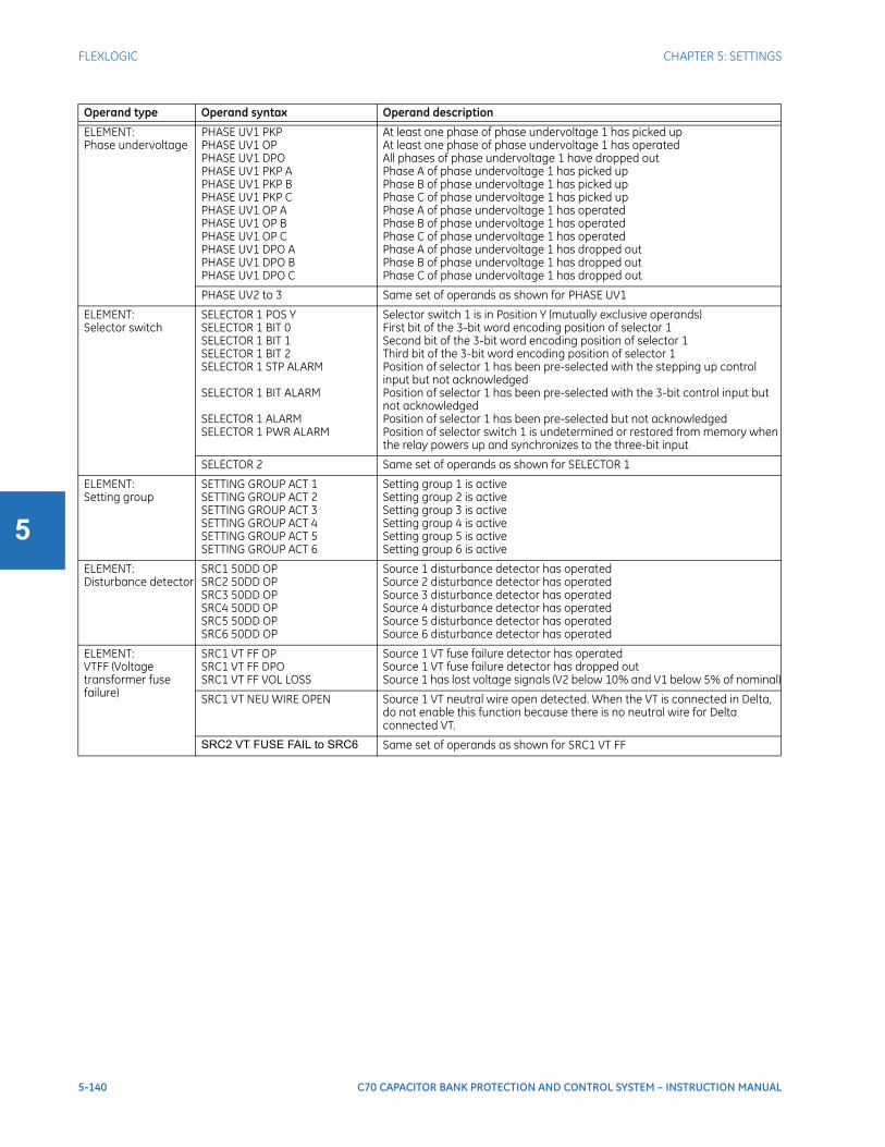
5-140 C70 CAPACITOR BANK PROTECTION AND CONTROL SYSTEM – INSTRUCTION MANUAL
FLEXLOGIC CHAPTER 5: SETTINGS
5
ELEMENT:Phase undervoltage
PHASE UV1 PKPPHASE UV1 OPPHASE UV1 DPOPHASE UV1 PKP APHASE UV1 PKP BPHASE UV1 PKP CPHASE UV1 OP APHASE UV1 OP BPHASE UV1 OP CPHASE UV1 DPO APHASE UV1 DPO BPHASE UV1 DPO C
At least one phase of phase undervoltage 1 has picked upAt least one phase of phase undervoltage 1 has operatedAll phases of phase undervoltage 1 have dropped outPhase A of phase undervoltage 1 has picked upPhase B of phase undervoltage 1 has picked upPhase C of phase undervoltage 1 has picked upPhase A of phase undervoltage 1 has operatedPhase B of phase undervoltage 1 has operatedPhase C of phase undervoltage 1 has operatedPhase A of phase undervoltage 1 has dropped outPhase B of phase undervoltage 1 has dropped outPhase C of phase undervoltage 1 has dropped out
PHASE UV2 to 3 Same set of operands as shown for PHASE UV1
ELEMENT:Selector switch
SELECTOR 1 POS YSELECTOR 1 BIT 0SELECTOR 1 BIT 1SELECTOR 1 BIT 2SELECTOR 1 STP ALARM
SELECTOR 1 BIT ALARM
SELECTOR 1 ALARMSELECTOR 1 PWR ALARM
Selector switch 1 is in Position Y (mutually exclusive operands)First bit of the 3-bit word encoding position of selector 1Second bit of the 3-bit word encoding position of selector 1Third bit of the 3-bit word encoding position of selector 1Position of selector 1 has been pre-selected with the stepping up control input but not acknowledgedPosition of selector 1 has been pre-selected with the 3-bit control input but not acknowledgedPosition of selector 1 has been pre-selected but not acknowledgedPosition of selector switch 1 is undetermined or restored from memory when the relay powers up and synchronizes to the three-bit input
SELECTOR 2 Same set of operands as shown for SELECTOR 1
ELEMENT:Setting group
SETTING GROUP ACT 1SETTING GROUP ACT 2SETTING GROUP ACT 3SETTING GROUP ACT 4SETTING GROUP ACT 5SETTING GROUP ACT 6
Setting group 1 is activeSetting group 2 is activeSetting group 3 is activeSetting group 4 is activeSetting group 5 is activeSetting group 6 is active
ELEMENT:Disturbance detector
SRC1 50DD OPSRC2 50DD OPSRC3 50DD OPSRC4 50DD OPSRC5 50DD OPSRC6 50DD OP
Source 1 disturbance detector has operatedSource 2 disturbance detector has operatedSource 3 disturbance detector has operatedSource 4 disturbance detector has operatedSource 5 disturbance detector has operatedSource 6 disturbance detector has operated
ELEMENT:VTFF (Voltage transformer fuse failure)
SRC1 VT FF OPSRC1 VT FF DPOSRC1 VT FF VOL LOSS
Source 1 VT fuse failure detector has operatedSource 1 VT fuse failure detector has dropped outSource 1 has lost voltage signals (V2 below 10% and V1 below 5% of nominal)
SRC1 VT NEU WIRE OPEN Source 1 VT neutral wire open detected. When the VT is connected in Delta, do not enable this function because there is no neutral wire for Delta connected VT.
SRC2 VT FUSE FAIL to SRC6 Same set of operands as shown for SRC1 VT FF
Operand type Operand syntax Operand description
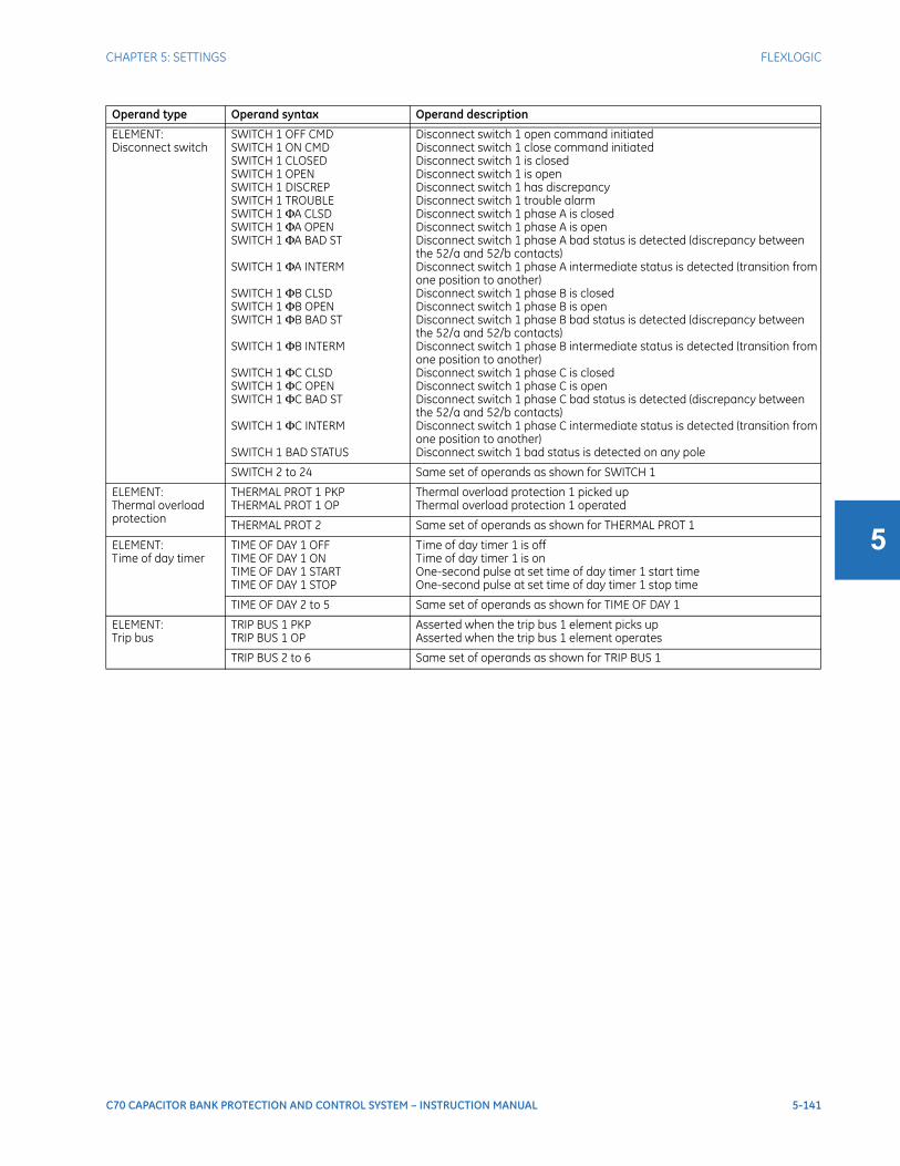
CHAPTER 5: SETTINGS FLEXLOGIC
C70 CAPACITOR BANK PROTECTION AND CONTROL SYSTEM – INSTRUCTION MANUAL 5-141
5
ELEMENT:Disconnect switch
SWITCH 1 OFF CMDSWITCH 1 ON CMDSWITCH 1 CLOSEDSWITCH 1 OPENSWITCH 1 DISCREPSWITCH 1 TROUBLESWITCH 1 ΦA CLSDSWITCH 1 ΦA OPENSWITCH 1 ΦA BAD ST
SWITCH 1 ΦA INTERM
SWITCH 1 ΦB CLSDSWITCH 1 ΦB OPENSWITCH 1 ΦB BAD ST
SWITCH 1 ΦB INTERM
SWITCH 1 ΦC CLSDSWITCH 1 ΦC OPENSWITCH 1 ΦC BAD ST
SWITCH 1 ΦC INTERM
SWITCH 1 BAD STATUS
Disconnect switch 1 open command initiatedDisconnect switch 1 close command initiatedDisconnect switch 1 is closedDisconnect switch 1 is openDisconnect switch 1 has discrepancyDisconnect switch 1 trouble alarmDisconnect switch 1 phase A is closedDisconnect switch 1 phase A is openDisconnect switch 1 phase A bad status is detected (discrepancy between the 52/a and 52/b contacts)Disconnect switch 1 phase A intermediate status is detected (transition from one position to another)Disconnect switch 1 phase B is closedDisconnect switch 1 phase B is openDisconnect switch 1 phase B bad status is detected (discrepancy between the 52/a and 52/b contacts)Disconnect switch 1 phase B intermediate status is detected (transition from one position to another)Disconnect switch 1 phase C is closedDisconnect switch 1 phase C is openDisconnect switch 1 phase C bad status is detected (discrepancy between the 52/a and 52/b contacts)Disconnect switch 1 phase C intermediate status is detected (transition from one position to another)Disconnect switch 1 bad status is detected on any pole
SWITCH 2 to 24 Same set of operands as shown for SWITCH 1
ELEMENT:Thermal overload protection
THERMAL PROT 1 PKPTHERMAL PROT 1 OP
Thermal overload protection 1 picked upThermal overload protection 1 operated
THERMAL PROT 2 Same set of operands as shown for THERMAL PROT 1
ELEMENT:Time of day timer
TIME OF DAY 1 OFFTIME OF DAY 1 ONTIME OF DAY 1 STARTTIME OF DAY 1 STOP
Time of day timer 1 is offTime of day timer 1 is onOne-second pulse at set time of day timer 1 start timeOne-second pulse at set time of day timer 1 stop time
TIME OF DAY 2 to 5 Same set of operands as shown for TIME OF DAY 1
ELEMENT:Trip bus
TRIP BUS 1 PKPTRIP BUS 1 OP
Asserted when the trip bus 1 element picks upAsserted when the trip bus 1 element operates
TRIP BUS 2 to 6 Same set of operands as shown for TRIP BUS 1
Operand type Operand syntax Operand description
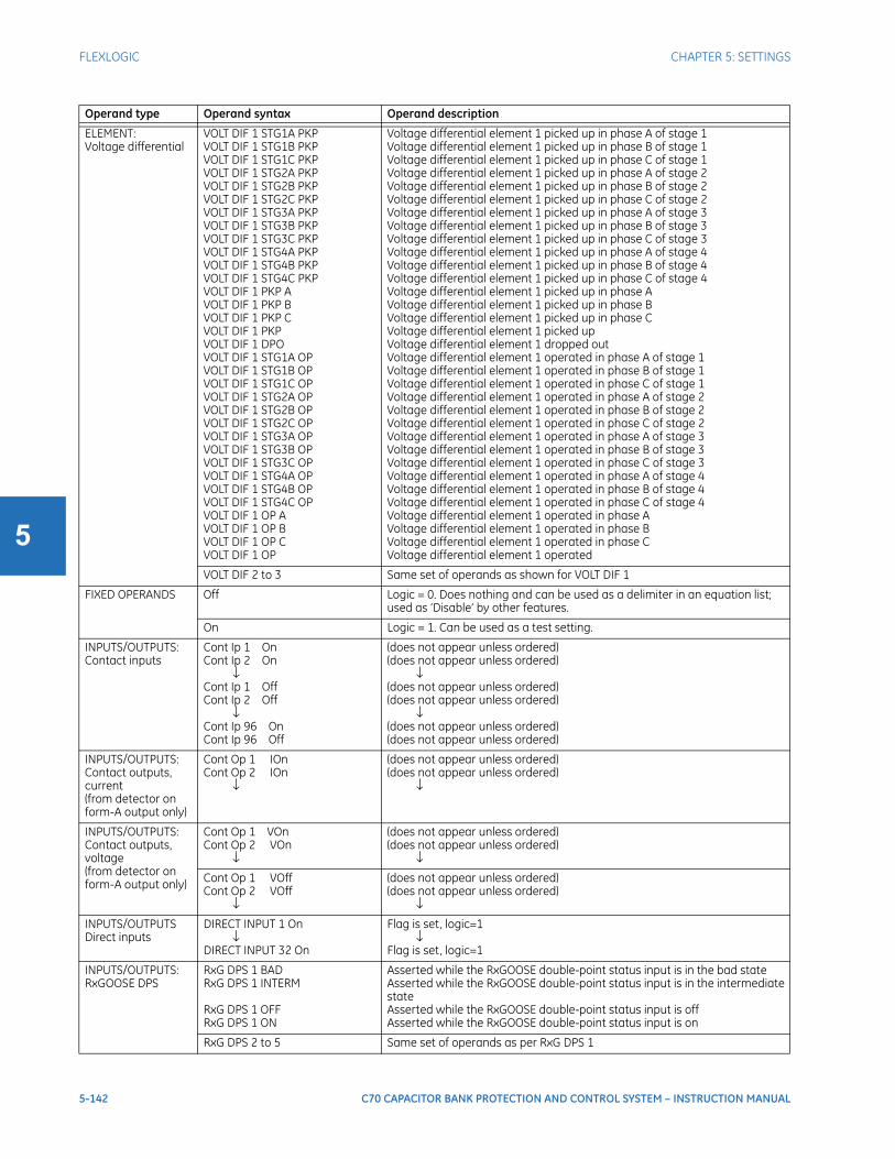
5-142 C70 CAPACITOR BANK PROTECTION AND CONTROL SYSTEM – INSTRUCTION MANUAL
FLEXLOGIC CHAPTER 5: SETTINGS
5
ELEMENT:Voltage differential
VOLT DIF 1 STG1A PKPVOLT DIF 1 STG1B PKPVOLT DIF 1 STG1C PKPVOLT DIF 1 STG2A PKPVOLT DIF 1 STG2B PKPVOLT DIF 1 STG2C PKPVOLT DIF 1 STG3A PKPVOLT DIF 1 STG3B PKPVOLT DIF 1 STG3C PKPVOLT DIF 1 STG4A PKPVOLT DIF 1 STG4B PKPVOLT DIF 1 STG4C PKPVOLT DIF 1 PKP AVOLT DIF 1 PKP BVOLT DIF 1 PKP CVOLT DIF 1 PKPVOLT DIF 1 DPOVOLT DIF 1 STG1A OPVOLT DIF 1 STG1B OPVOLT DIF 1 STG1C OPVOLT DIF 1 STG2A OPVOLT DIF 1 STG2B OPVOLT DIF 1 STG2C OPVOLT DIF 1 STG3A OPVOLT DIF 1 STG3B OPVOLT DIF 1 STG3C OPVOLT DIF 1 STG4A OPVOLT DIF 1 STG4B OPVOLT DIF 1 STG4C OPVOLT DIF 1 OP AVOLT DIF 1 OP BVOLT DIF 1 OP CVOLT DIF 1 OP
Voltage differential element 1 picked up in phase A of stage 1Voltage differential element 1 picked up in phase B of stage 1Voltage differential element 1 picked up in phase C of stage 1Voltage differential element 1 picked up in phase A of stage 2Voltage differential element 1 picked up in phase B of stage 2Voltage differential element 1 picked up in phase C of stage 2Voltage differential element 1 picked up in phase A of stage 3Voltage differential element 1 picked up in phase B of stage 3Voltage differential element 1 picked up in phase C of stage 3Voltage differential element 1 picked up in phase A of stage 4Voltage differential element 1 picked up in phase B of stage 4Voltage differential element 1 picked up in phase C of stage 4Voltage differential element 1 picked up in phase AVoltage differential element 1 picked up in phase BVoltage differential element 1 picked up in phase CVoltage differential element 1 picked upVoltage differential element 1 dropped outVoltage differential element 1 operated in phase A of stage 1Voltage differential element 1 operated in phase B of stage 1Voltage differential element 1 operated in phase C of stage 1Voltage differential element 1 operated in phase A of stage 2Voltage differential element 1 operated in phase B of stage 2Voltage differential element 1 operated in phase C of stage 2Voltage differential element 1 operated in phase A of stage 3Voltage differential element 1 operated in phase B of stage 3Voltage differential element 1 operated in phase C of stage 3Voltage differential element 1 operated in phase A of stage 4Voltage differential element 1 operated in phase B of stage 4Voltage differential element 1 operated in phase C of stage 4Voltage differential element 1 operated in phase AVoltage differential element 1 operated in phase BVoltage differential element 1 operated in phase CVoltage differential element 1 operated
VOLT DIF 2 to 3 Same set of operands as shown for VOLT DIF 1
FIXED OPERANDS Off Logic = 0. Does nothing and can be used as a delimiter in an equation list; used as ‘Disable’ by other features.
On Logic = 1. Can be used as a test setting.
INPUTS/OUTPUTS:Contact inputs
Cont Ip 1 OnCont Ip 2 On
↓Cont Ip 1 OffCont Ip 2 Off
↓Cont Ip 96 OnCont Ip 96 Off
(does not appear unless ordered)(does not appear unless ordered)
↓(does not appear unless ordered)(does not appear unless ordered)
↓(does not appear unless ordered)(does not appear unless ordered)
INPUTS/OUTPUTS:Contact outputs, current(from detector on form-A output only)
Cont Op 1 IOnCont Op 2 IOn
↓
(does not appear unless ordered)(does not appear unless ordered)
↓
INPUTS/OUTPUTS:Contact outputs, voltage(from detector on form-A output only)
Cont Op 1 VOnCont Op 2 VOn
↓
(does not appear unless ordered)(does not appear unless ordered)
↓Cont Op 1 VOffCont Op 2 VOff
↓
(does not appear unless ordered)(does not appear unless ordered)
↓INPUTS/OUTPUTSDirect inputs
DIRECT INPUT 1 On↓
DIRECT INPUT 32 On
Flag is set, logic=1↓
Flag is set, logic=1
INPUTS/OUTPUTS:RxGOOSE DPS
RxG DPS 1 BADRxG DPS 1 INTERM
RxG DPS 1 OFFRxG DPS 1 ON
Asserted while the RxGOOSE double-point status input is in the bad stateAsserted while the RxGOOSE double-point status input is in the intermediate stateAsserted while the RxGOOSE double-point status input is offAsserted while the RxGOOSE double-point status input is on
RxG DPS 2 to 5 Same set of operands as per RxG DPS 1
Operand type Operand syntax Operand description
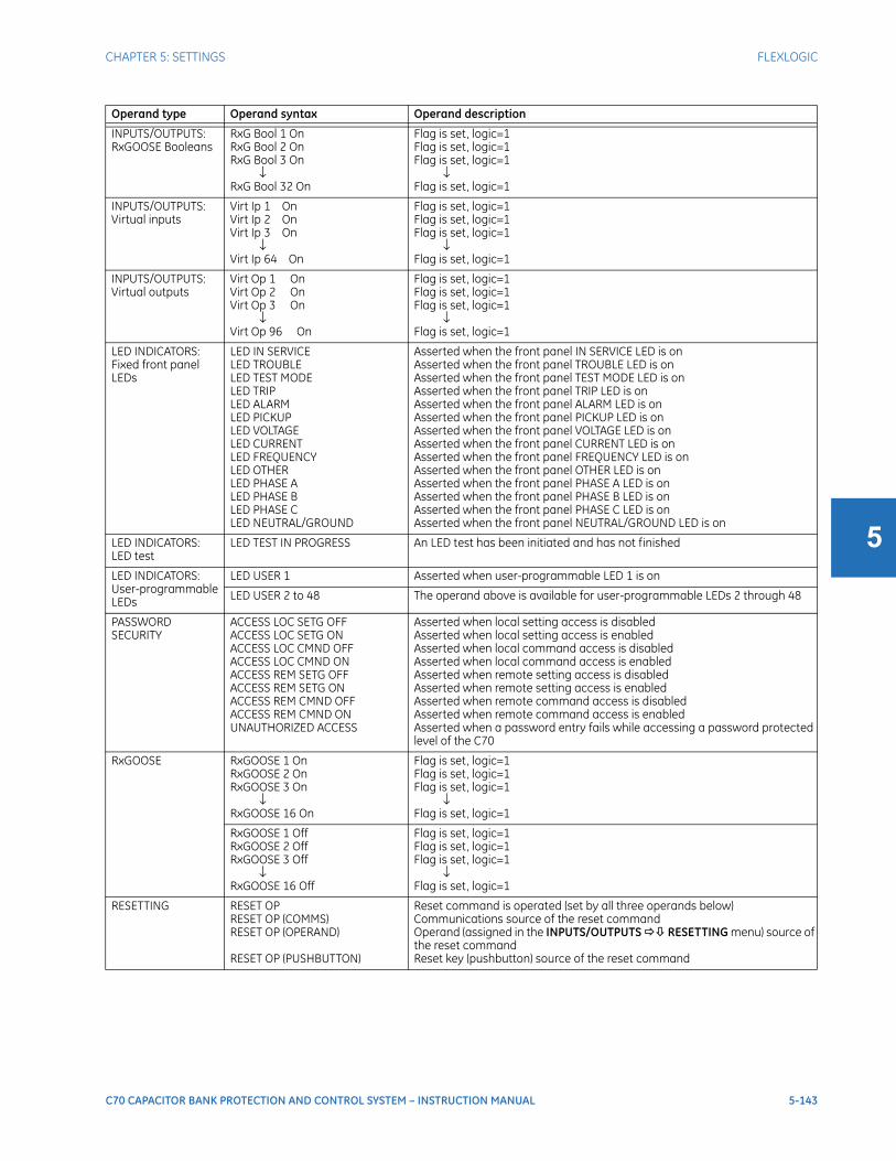
CHAPTER 5: SETTINGS FLEXLOGIC
C70 CAPACITOR BANK PROTECTION AND CONTROL SYSTEM – INSTRUCTION MANUAL 5-143
5
INPUTS/OUTPUTS:RxGOOSE Booleans
RxG Bool 1 OnRxG Bool 2 OnRxG Bool 3 On
↓RxG Bool 32 On
Flag is set, logic=1Flag is set, logic=1Flag is set, logic=1
↓Flag is set, logic=1
INPUTS/OUTPUTS:Virtual inputs
Virt Ip 1 OnVirt Ip 2 OnVirt Ip 3 On
↓Virt Ip 64 On
Flag is set, logic=1Flag is set, logic=1Flag is set, logic=1
↓Flag is set, logic=1
INPUTS/OUTPUTS:Virtual outputs
Virt Op 1 OnVirt Op 2 OnVirt Op 3 On
↓Virt Op 96 On
Flag is set, logic=1Flag is set, logic=1Flag is set, logic=1
↓Flag is set, logic=1
LED INDICATORS:Fixed front panel LEDs
LED IN SERVICELED TROUBLELED TEST MODELED TRIPLED ALARMLED PICKUPLED VOLTAGELED CURRENTLED FREQUENCYLED OTHERLED PHASE ALED PHASE BLED PHASE CLED NEUTRAL/GROUND
Asserted when the front panel IN SERVICE LED is onAsserted when the front panel TROUBLE LED is onAsserted when the front panel TEST MODE LED is onAsserted when the front panel TRIP LED is onAsserted when the front panel ALARM LED is onAsserted when the front panel PICKUP LED is onAsserted when the front panel VOLTAGE LED is onAsserted when the front panel CURRENT LED is onAsserted when the front panel FREQUENCY LED is onAsserted when the front panel OTHER LED is onAsserted when the front panel PHASE A LED is onAsserted when the front panel PHASE B LED is onAsserted when the front panel PHASE C LED is onAsserted when the front panel NEUTRAL/GROUND LED is on
LED INDICATORS:LED test
LED TEST IN PROGRESS An LED test has been initiated and has not finished
LED INDICATORS:User-programmable LEDs
LED USER 1 Asserted when user-programmable LED 1 is on
LED USER 2 to 48 The operand above is available for user-programmable LEDs 2 through 48
PASSWORD SECURITY
ACCESS LOC SETG OFFACCESS LOC SETG ONACCESS LOC CMND OFFACCESS LOC CMND ONACCESS REM SETG OFFACCESS REM SETG ONACCESS REM CMND OFFACCESS REM CMND ONUNAUTHORIZED ACCESS
Asserted when local setting access is disabledAsserted when local setting access is enabledAsserted when local command access is disabledAsserted when local command access is enabledAsserted when remote setting access is disabledAsserted when remote setting access is enabledAsserted when remote command access is disabledAsserted when remote command access is enabledAsserted when a password entry fails while accessing a password protected level of the C70
RxGOOSE RxGOOSE 1 OnRxGOOSE 2 OnRxGOOSE 3 On
↓RxGOOSE 16 On
Flag is set, logic=1Flag is set, logic=1Flag is set, logic=1
↓Flag is set, logic=1
RxGOOSE 1 OffRxGOOSE 2 OffRxGOOSE 3 Off
↓RxGOOSE 16 Off
Flag is set, logic=1Flag is set, logic=1Flag is set, logic=1
↓Flag is set, logic=1
RESETTING RESET OPRESET OP (COMMS)RESET OP (OPERAND)
RESET OP (PUSHBUTTON)
Reset command is operated (set by all three operands below)Communications source of the reset commandOperand (assigned in the INPUTS/OUTPUTS RESETTING menu) source of the reset commandReset key (pushbutton) source of the reset command
Operand type Operand syntax Operand description
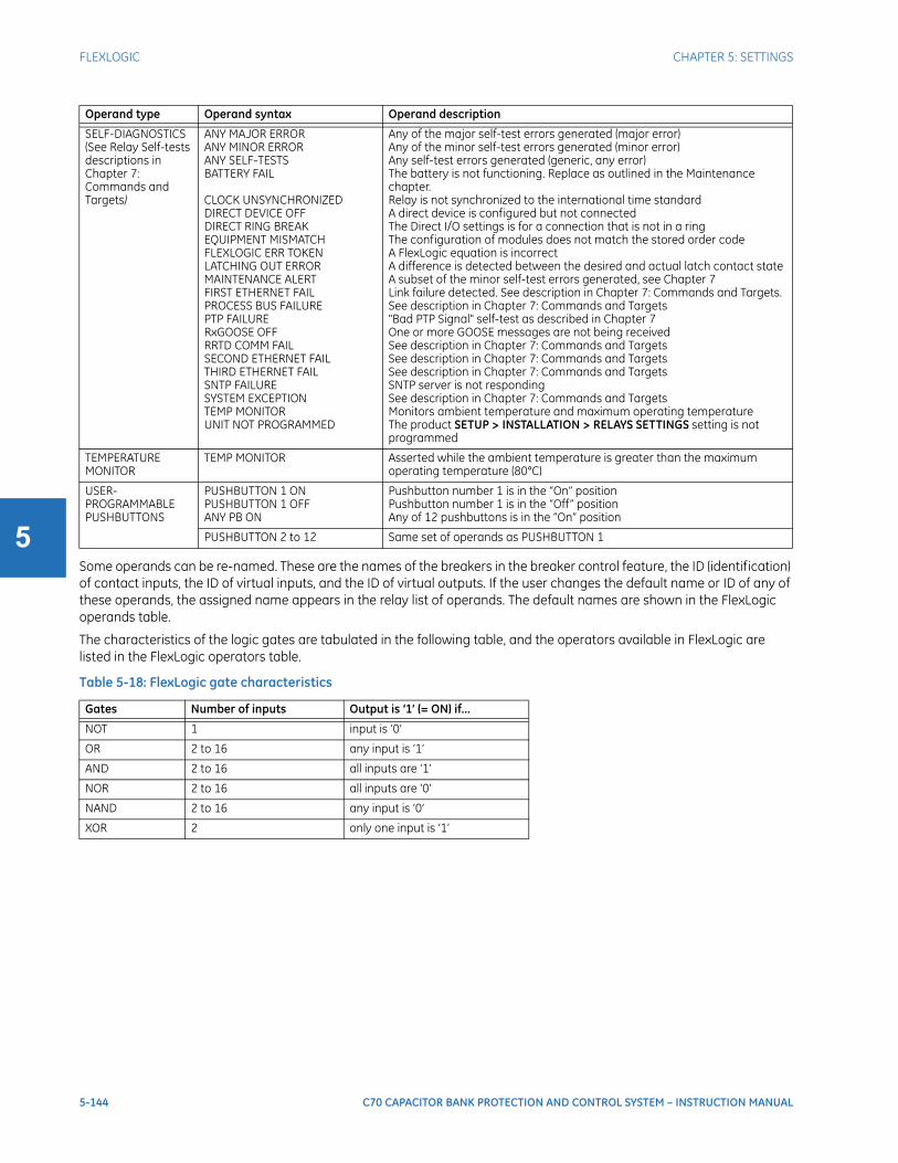
5-144 C70 CAPACITOR BANK PROTECTION AND CONTROL SYSTEM – INSTRUCTION MANUAL
FLEXLOGIC CHAPTER 5: SETTINGS
5Some operands can be re-named. These are the names of the breakers in the breaker control feature, the ID (identification) of contact inputs, the ID of virtual inputs, and the ID of virtual outputs. If the user changes the default name or ID of any of these operands, the assigned name appears in the relay list of operands. The default names are shown in the FlexLogic operands table.
The characteristics of the logic gates are tabulated in the following table, and the operators available in FlexLogic are listed in the FlexLogic operators table.
Table 5-18: FlexLogic gate characteristics
SELF-DIAGNOSTICS(See Relay Self-tests descriptions in Chapter 7: Commands and Targets)
ANY MAJOR ERRORANY MINOR ERRORANY SELF-TESTSBATTERY FAIL
CLOCK UNSYNCHRONIZEDDIRECT DEVICE OFFDIRECT RING BREAKEQUIPMENT MISMATCHFLEXLOGIC ERR TOKENLATCHING OUT ERRORMAINTENANCE ALERTFIRST ETHERNET FAILPROCESS BUS FAILUREPTP FAILURERxGOOSE OFFRRTD COMM FAILSECOND ETHERNET FAILTHIRD ETHERNET FAILSNTP FAILURESYSTEM EXCEPTIONTEMP MONITORUNIT NOT PROGRAMMED
Any of the major self-test errors generated (major error)Any of the minor self-test errors generated (minor error)Any self-test errors generated (generic, any error)The battery is not functioning. Replace as outlined in the Maintenance chapter.Relay is not synchronized to the international time standardA direct device is configured but not connectedThe Direct I/O settings is for a connection that is not in a ringThe configuration of modules does not match the stored order codeA FlexLogic equation is incorrectA difference is detected between the desired and actual latch contact stateA subset of the minor self-test errors generated, see Chapter 7Link failure detected. See description in Chapter 7: Commands and Targets.See description in Chapter 7: Commands and Targets"Bad PTP Signal" self-test as described in Chapter 7One or more GOOSE messages are not being receivedSee description in Chapter 7: Commands and TargetsSee description in Chapter 7: Commands and TargetsSee description in Chapter 7: Commands and TargetsSNTP server is not respondingSee description in Chapter 7: Commands and TargetsMonitors ambient temperature and maximum operating temperatureThe product SETUP > INSTALLATION > RELAYS SETTINGS setting is not programmed
TEMPERATURE MONITOR
TEMP MONITOR Asserted while the ambient temperature is greater than the maximum operating temperature (80°C)
USER-PROGRAMMABLE PUSHBUTTONS
PUSHBUTTON 1 ONPUSHBUTTON 1 OFFANY PB ON
Pushbutton number 1 is in the “On” positionPushbutton number 1 is in the “Off” positionAny of 12 pushbuttons is in the “On” position
PUSHBUTTON 2 to 12 Same set of operands as PUSHBUTTON 1
Gates Number of inputs Output is ‘1’ (= ON) if...
NOT 1 input is ‘0’
OR 2 to 16 any input is ‘1’
AND 2 to 16 all inputs are ‘1’
NOR 2 to 16 all inputs are ‘0’
NAND 2 to 16 any input is ‘0’
XOR 2 only one input is ‘1’
Operand type Operand syntax Operand description

CHAPTER 5: SETTINGS FLEXLOGIC
C70 CAPACITOR BANK PROTECTION AND CONTROL SYSTEM – INSTRUCTION MANUAL 5-145
5
Table 5-19: FlexLogic operators
5.6.2 FlexLogic rulesWhen forming a FlexLogic equation, the sequence in the linear array of parameters must follow these general rules:
1. Operands must precede the operator that uses the operands as inputs.
2. Operators have only one output. The output of an operator must be used to create a virtual output if it is to be used as an input to two or more operators.
3. Assigning the output of an operator to a virtual output terminates the equation.
4. A timer operator (for example, "TIMER 1") or virtual output assignment (for example, " = Virt Op 1") can be used once only. If this rule is broken, a syntax error is declared.
5.6.3 FlexLogic evaluationEach equation is evaluated in the ascending order in which the parameters have been entered.
Type Syntax Description Notes
Editor INSERT Insert a parameter in an equation list
DELETE Delete a parameter from an equation list
End END The first END encountered signifies the last entry in the list of processed FlexLogic parameters
One-shot POSITIVE ONE SHOT One shot that responds to a positive going edge A ‘one shot’ refers to a single input gate that generates a pulse in response to an edge on the input. The output from a ‘one shot’ is True (positive) for only one pass through the FlexLogic equation. There is a maximum of 64 ‘one shots.’
NEGATIVE ONE SHOT One shot that responds to a negative going edge
DUAL ONE SHOT One shot that responds to both the positive and negative going edges
Logicgate
NOT Logical NOT Operates on the previous parameter
OR(2)↓
OR(16)
2 input OR gate↓
16 input OR gate
Operates on the 2 previous parameters↓
Operates on the 16 previous parameters
AND(2)↓
AND(16)
2 input AND gate↓
16 input AND gate
Operates on the 2 previous parameters↓
Operates on the 16 previous parameters
NOR(2)↓
NOR(16)
2 input NOR gate↓
16 input NOR gate
Operates on the 2 previous parameters↓
Operates on the 16 previous parameters
NAND(2)↓
NAND(16)
2 input NAND gate↓
16 input NAND gate
Operates on the 2 previous parameters↓
Operates on the 16 previous parameters
XOR(2) 2 input Exclusive OR gate Operates on the 2 previous parameters
LATCH (S,R) Latch (set, reset): reset-dominant The parameter preceding LATCH(S,R) is the reset input. The parameter preceding the reset input is the set input.
Timer TIMER 1↓
TIMER 32
Timer set with FlexLogic timer 1 settings↓
Timer set with FlexLogic timer 32 settings
The timer is started by the preceding parameter. The output of the timer is TIMER #.
Assign virtualoutput
= Virt Op 1↓
= Virt Op 96
Assigns previous FlexLogic operand to virtual output 1
↓Assigns previous FlexLogic operand to virtual output 96
The virtual output is set by the preceding parameter
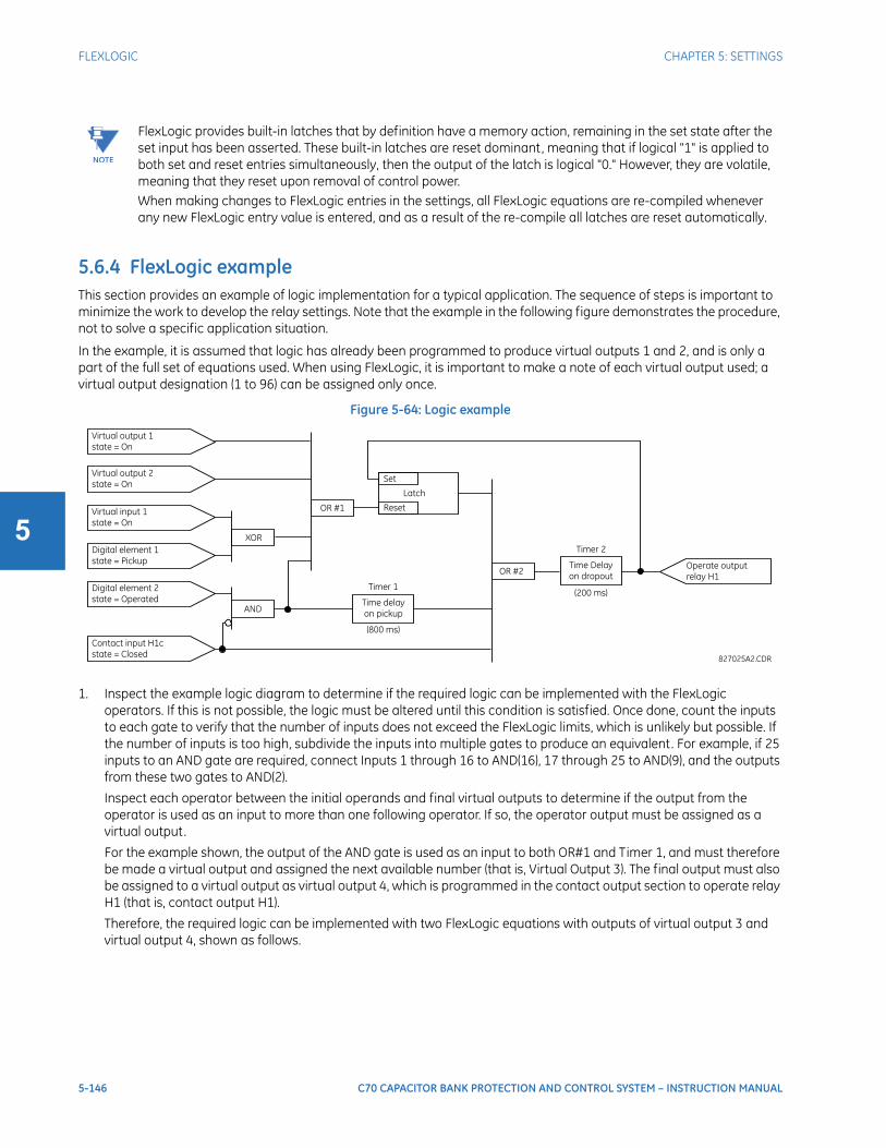
5-146 C70 CAPACITOR BANK PROTECTION AND CONTROL SYSTEM – INSTRUCTION MANUAL
FLEXLOGIC CHAPTER 5: SETTINGS
5
5.6.4 FlexLogic exampleThis section provides an example of logic implementation for a typical application. The sequence of steps is important to minimize the work to develop the relay settings. Note that the example in the following figure demonstrates the procedure, not to solve a specific application situation.
In the example, it is assumed that logic has already been programmed to produce virtual outputs 1 and 2, and is only a part of the full set of equations used. When using FlexLogic, it is important to make a note of each virtual output used; a virtual output designation (1 to 96) can be assigned only once.
Figure 5-64: Logic example
1. Inspect the example logic diagram to determine if the required logic can be implemented with the FlexLogic operators. If this is not possible, the logic must be altered until this condition is satisfied. Once done, count the inputs to each gate to verify that the number of inputs does not exceed the FlexLogic limits, which is unlikely but possible. If the number of inputs is too high, subdivide the inputs into multiple gates to produce an equivalent. For example, if 25 inputs to an AND gate are required, connect Inputs 1 through 16 to AND(16), 17 through 25 to AND(9), and the outputs from these two gates to AND(2).
Inspect each operator between the initial operands and final virtual outputs to determine if the output from the operator is used as an input to more than one following operator. If so, the operator output must be assigned as a virtual output.
For the example shown, the output of the AND gate is used as an input to both OR#1 and Timer 1, and must therefore be made a virtual output and assigned the next available number (that is, Virtual Output 3). The final output must also be assigned to a virtual output as virtual output 4, which is programmed in the contact output section to operate relay H1 (that is, contact output H1).
Therefore, the required logic can be implemented with two FlexLogic equations with outputs of virtual output 3 and virtual output 4, shown as follows.
NOTE
FlexLogic provides built-in latches that by definition have a memory action, remaining in the set state after the set input has been asserted. These built-in latches are reset dominant, meaning that if logical "1" is applied to both set and reset entries simultaneously, then the output of the latch is logical "0." However, they are volatile, meaning that they reset upon removal of control power.When making changes to FlexLogic entries in the settings, all FlexLogic equations are re-compiled whenever any new FlexLogic entry value is entered, and as a result of the re-compile all latches are reset automatically.

CHAPTER 5: SETTINGS FLEXLOGIC
C70 CAPACITOR BANK PROTECTION AND CONTROL SYSTEM – INSTRUCTION MANUAL 5-147
5
Figure 5-65: Logic example with virtual outputs
2. Prepare a logic diagram for the equation to produce virtual output 3, as this output is used as an operand in the virtual output 4 equation (create the equation for every output that is used as an operand first , so that when these operands are required they already have been evaluated and assigned to a specific virtual output). The logic for virtual output 3 is shown as follows with the final output assigned.
Figure 5-66: Logic for virtual output 3
3. Prepare a logic diagram for virtual output 4, replacing the logic ahead of virtual output 3 with a symbol identified as virtual output 3, shown as follows.
Figure 5-67: Logic for virtual output 4
4. Program the FlexLogic equation for virtual output 3 by translating the logic into available FlexLogic parameters. The equation is formed one parameter at a time until the required logic is complete. It is generally easier to start at the output end of the equation and work back towards the input, as shown in the following steps. It is also recommended

5-148 C70 CAPACITOR BANK PROTECTION AND CONTROL SYSTEM – INSTRUCTION MANUAL
FLEXLOGIC CHAPTER 5: SETTINGS
5
to list operator inputs from bottom to top. For demonstration, the final outputs are arbitrarily identified as parameter 99, and each preceding parameter decremented by one in turn. Until accustomed to using FlexLogic, it is suggested that a worksheet with a series of cells marked with the arbitrary parameter numbers be prepared shown as follows.
Figure 5-68: FlexLogic worksheet
5. Following the procedure outlined, start with parameter 99, as follows:
– 99: The final output of the equation is virtual output 3, which is created by the operator "= Virt Op n". This parameter is therefore "= Virt Op 3".
– 98: The gate preceding the output is an AND, which in this case requires two inputs. The operator for this gate is a 2-input AND so the parameter is “AND(2)”. Note that FlexLogic rules require that the number of inputs to most types of operators must be specified to identify the operands for the gate. As the 2-input AND operates on the two operands preceding it , these inputs must be specified, starting with the lower.
– 97: This lower input to the AND gate must be passed through an inverter (the NOT operator) so the next parameter is “NOT”. The NOT operator acts upon the operand immediately preceding it , so specify the inverter input next.
– 96: The input to the NOT gate is to be contact input H1c. The ON state of a contact input can be programmed to be set when the contact is either open or closed. Assume for this example that the state is to be ON for a closed contact. The operand is therefore “Cont Ip H1c On”.
– 95: The last step in the procedure is to specify the upper input to the AND gate, the operated state of digital element 2. This operand is "DIG ELEM 2 OP".
Writing the parameters in numerical order forms the equation for virtual output 3:[95] DIG ELEM 2 OP[96] Cont Ip H1c On
[97] NOT
[98] AND(2)[99] = Virt Op 3
It is now possible to check that this selection of parameters produces the required logic by converting the set of parameters into a logic diagram. The result of this process is shown in the figure, which is compared to the logic for virtual output 3 diagram as a check.
01
02
03
04
05
97
98
99
.....
827029A1.VSD
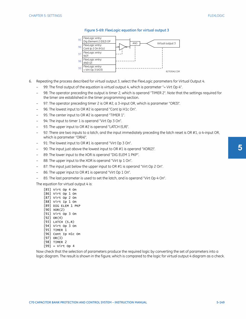
CHAPTER 5: SETTINGS FLEXLOGIC
C70 CAPACITOR BANK PROTECTION AND CONTROL SYSTEM – INSTRUCTION MANUAL 5-149
5
Figure 5-69: FlexLogic equation for virtual output 3
6. Repeating the process described for virtual output 3, select the FlexLogic parameters for Virtual Output 4.
– 99: The final output of the equation is virtual output 4, which is parameter “= Virt Op 4".
– 98: The operator preceding the output is timer 2, which is operand “TIMER 2". Note that the settings required for the timer are established in the timer programming section.
– 97: The operator preceding timer 2 is OR #2, a 3-input OR, which is parameter “OR(3)”.
– 96: The lowest input to OR #2 is operand “Cont Ip H1c On”.
– 95: The center input to OR #2 is operand “TIMER 1".
– 94: The input to timer 1 is operand “Virt Op 3 On".
– 93: The upper input to OR #2 is operand “LATCH (S,R)”.
– 92: There are two inputs to a latch, and the input immediately preceding the latch reset is OR #1, a 4-input OR, which is parameter “OR(4)”.
– 91: The lowest input to OR #1 is operand “Virt Op 3 On".
– 90: The input just above the lowest input to OR #1 is operand “XOR(2)”.
– 89: The lower input to the XOR is operand “DIG ELEM 1 PKP”.
– 88: The upper input to the XOR is operand “Virt Ip 1 On".
– 87: The input just below the upper input to OR #1 is operand “Virt Op 2 On".
– 86: The upper input to OR #1 is operand “Virt Op 1 On".
– 85: The last parameter is used to set the latch, and is operand “Virt Op 4 On".
The equation for virtual output 4 is:[85] Virt Op 4 On
[86] Virt Op 1 On[87] Virt Op 2 On
[88] Virt Ip 1 On
[89] DIG ELEM 1 PKP[90] XOR(2)
[91] Virt Op 3 On
[92] OR(4)[93] LATCH (S,R)
[94] Virt Op 3 On
[95] TIMER 1[96] Cont Ip H1c On
[97] OR(3)
[98] TIMER 2[99] = Virt Op 4
Now check that the selection of parameters produce the required logic by converting the set of parameters into a logic diagram. The result is shown in the figure, which is compared to the logic for virtual output 4 diagram as a check.
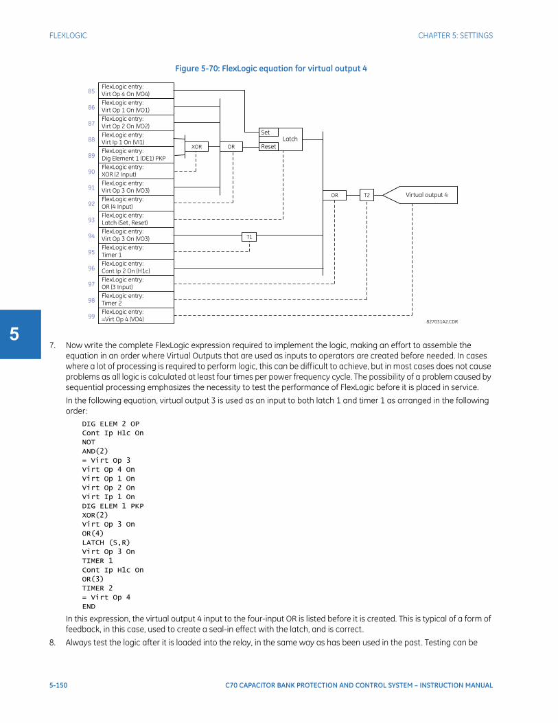
5-150 C70 CAPACITOR BANK PROTECTION AND CONTROL SYSTEM – INSTRUCTION MANUAL
FLEXLOGIC CHAPTER 5: SETTINGS
5
Figure 5-70: FlexLogic equation for virtual output 4
7. Now write the complete FlexLogic expression required to implement the logic, making an effort to assemble the equation in an order where Virtual Outputs that are used as inputs to operators are created before needed. In cases where a lot of processing is required to perform logic, this can be difficult to achieve, but in most cases does not cause problems as all logic is calculated at least four times per power frequency cycle. The possibility of a problem caused by sequential processing emphasizes the necessity to test the performance of FlexLogic before it is placed in service.
In the following equation, virtual output 3 is used as an input to both latch 1 and timer 1 as arranged in the following order:
DIG ELEM 2 OP
Cont Ip H1c OnNOT
AND(2)
= Virt Op 3Virt Op 4 On
Virt Op 1 On
Virt Op 2 OnVirt Ip 1 On
DIG ELEM 1 PKP
XOR(2)Virt Op 3 On
OR(4)
LATCH (S,R)Virt Op 3 On
TIMER 1
Cont Ip H1c OnOR(3)
TIMER 2
= Virt Op 4END
In this expression, the virtual output 4 input to the four-input OR is listed before it is created. This is typical of a form of feedback, in this case, used to create a seal-in effect with the latch, and is correct.
8. Always test the logic after it is loaded into the relay, in the same way as has been used in the past. Testing can be
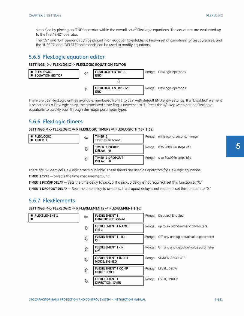
CHAPTER 5: SETTINGS FLEXLOGIC
C70 CAPACITOR BANK PROTECTION AND CONTROL SYSTEM – INSTRUCTION MANUAL 5-151
5
simplified by placing an "END" operator within the overall set of FlexLogic equations. The equations are evaluated up to the first "END" operator.
The "On" and "Off" operands can be placed in an equation to establish a known set of conditions for test purposes, and the "INSERT" and "DELETE" commands can be used to modify equations.
5.6.5 FlexLogic equation editorSETTINGS FLEXLOGIC FLEXLOGIC EQUATION EDITOR
There are 512 FlexLogic entries available, numbered from 1 to 512, with default END entry settings. If a "Disabled" element is selected as a FlexLogic entry, the associated state flag is never set to ‘1’. Press the +/– key when editing FlexLogic equations to quickly scan through the major parameter types.
5.6.6 FlexLogic timersSETTINGS FLEXLOGIC FLEXLOGIC TIMERS FLEXLOGIC TIMER 1(32)
There are 32 identical FlexLogic timers available. These timers are used as operators for FlexLogic equations.
TIMER 1 TYPE — Selects the time measurement unit.
TIMER 1 PICKUP DELAY — Sets the time delay to pickup. If a pickup delay is not required, set this function to "0."
TIMER 1 DROPOUT DELAY — Sets the time delay to dropout. If a dropout delay is not required, set this function to "0."
5.6.7 FlexElementsSETTINGS FLEXLOGIC FLEXELEMENTS FLEXELEMENT 1(16)
FLEXLOGIC EQUATION EDITOR FLEXLOGIC ENTRY 1:
ENDRange: FlexLogic operands
FLEXLOGIC ENTRY 512:END
Range: FlexLogic operands
FLEXLOGIC TIMER 1 TIMER 1
TYPE: millisecondRange: millisecond, second, minute
TIMER 1 PICKUPDELAY: 0
Range: 0 to 60000 in steps of 1
TIMER 1 DROPOUTDELAY: 0
Range: 0 to 60000 in steps of 1
FLEXELEMENT 1 FLEXELEMENT 1
FUNCTION: DisabledRange: Disabled, Enabled
FLEXELEMENT 1 NAME:FxE 1
Range: up to six alphanumeric characters
FLEXELEMENT 1 +IN:Off
Range: Off, any analog actual value parameter
FLEXELEMENT 1 -IN:Off
Range: Off, any analog actual value parameter
FLEXELEMENT 1 INPUTMODE: SIGNED
Range: SIGNED, ABSOLUTE
FLEXELEMENT 1 COMPMODE: LEVEL
Range: LEVEL, DELTA
FLEXELEMENT 1DIRECTION: OVER
Range: OVER, UNDER

5-152 C70 CAPACITOR BANK PROTECTION AND CONTROL SYSTEM – INSTRUCTION MANUAL
FLEXLOGIC CHAPTER 5: SETTINGS
5
A FlexElement is a universal comparator used to monitor any analog actual value calculated by the relay or a net difference of any two analog actual values of the same type. The effective operating signal can be treated as a signed number or its absolute value can be used.
FlexElements run every half power cycle (every four protection passes).
The element can be programmed to respond either to a signal level or to a rate-of-change (delta) over a pre-defined period of time. The output operand is asserted when the operating signal is higher than a threshold or lower than a threshold, as per your choice.
Figure 5-71: FlexElement logic
FLEXELEMENT 1 +IN — This setting specifies the first (non-inverted) input to the FlexElement. Zero is assumed as the input if this setting is set to “Off.” For proper operation of the element, at least one input must be selected. Otherwise, the element does not assert its output operands.
FLEXELEMENT 1PICKUP: 1.000 pu
Range: –90.000 to 90.000 pu in steps of 0.001
FLEXELEMENT 1HYSTERESIS: 3.0%
Range: 0.1 to 50.0% in steps of 0.1
FLEXELEMENT 1 dtUNIT: Milliseconds
Range: Milliseconds, Seconds, Minutes
FLEXELEMENT 1 dt:20
Range: 20 to 86400 in steps of 1
FLEXELEMENT 1 PKPDELAY: 0.000 s
Range: 0.000 to 65.535 s in steps of 0.001
FLEXELEMENT 1 RSTDELAY: 0.000 s
Range: 0.000 to 65.535 s in steps of 0.001
FLEXELEMENT 1 BLK:Off
Range: FlexLogic operand
FLEXELEMENT 1TARGET: Self-reset
Range: Self-reset, Disabled, Latched
FLEXELEMENT 1EVENTS: Disabled
Range: Disabled, Enabled
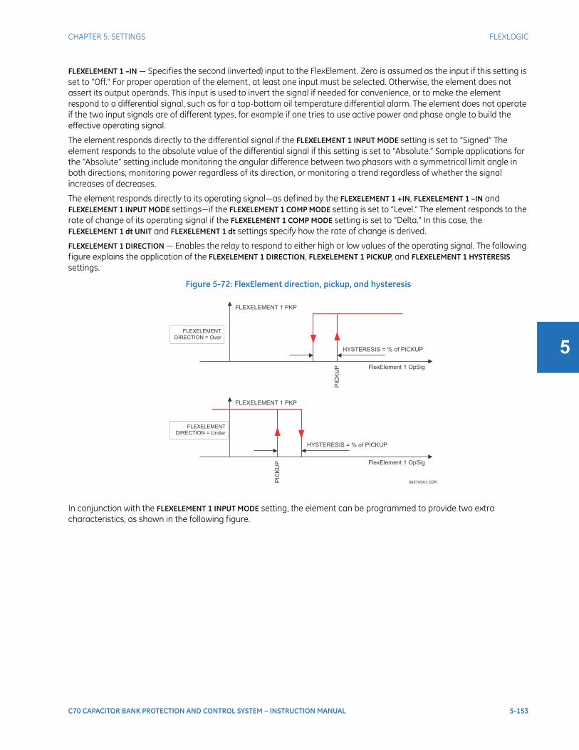
CHAPTER 5: SETTINGS FLEXLOGIC
C70 CAPACITOR BANK PROTECTION AND CONTROL SYSTEM – INSTRUCTION MANUAL 5-153
5
FLEXELEMENT 1 –IN — Specifies the second (inverted) input to the FlexElement. Zero is assumed as the input if this setting is set to “Off.” For proper operation of the element, at least one input must be selected. Otherwise, the element does not assert its output operands. This input is used to invert the signal if needed for convenience, or to make the element respond to a differential signal, such as for a top-bottom oil temperature differential alarm. The element does not operate if the two input signals are of different types, for example if one tries to use active power and phase angle to build the effective operating signal.
The element responds directly to the differential signal if the FLEXELEMENT 1 INPUT MODE setting is set to “Signed” The element responds to the absolute value of the differential signal if this setting is set to “Absolute.” Sample applications for the “Absolute” setting include monitoring the angular difference between two phasors with a symmetrical limit angle in both directions; monitoring power regardless of its direction, or monitoring a trend regardless of whether the signal increases of decreases.
The element responds directly to its operating signal—as defined by the FLEXELEMENT 1 +IN, FLEXELEMENT 1 –IN and FLEXELEMENT 1 INPUT MODE settings—if the FLEXELEMENT 1 COMP MODE setting is set to “Level.” The element responds to the rate of change of its operating signal if the FLEXELEMENT 1 COMP MODE setting is set to “Delta.” In this case, the FLEXELEMENT 1 dt UNIT and FLEXELEMENT 1 dt settings specify how the rate of change is derived.
FLEXELEMENT 1 DIRECTION — Enables the relay to respond to either high or low values of the operating signal. The following figure explains the application of the FLEXELEMENT 1 DIRECTION, FLEXELEMENT 1 PICKUP, and FLEXELEMENT 1 HYSTERESIS settings.
Figure 5-72: FlexElement direction, pickup, and hysteresis
In conjunction with the FLEXELEMENT 1 INPUT MODE setting, the element can be programmed to provide two extra characteristics, as shown in the following figure.
FlexElement 1 OpSig
FLEXELEMENT 1 PKP
FLEXELEMENT
DIRECTION = OverP
ICK
UP
HYSTERESIS = % of PICKUP
FlexElement 1 OpSig
FLEXELEMENT 1 PKP
FLEXELEMENT
DIRECTION = Under
PIC
KU
P
HYSTERESIS = % of PICKUP
842705A1.CDR

5-154 C70 CAPACITOR BANK PROTECTION AND CONTROL SYSTEM – INSTRUCTION MANUAL
FLEXLOGIC CHAPTER 5: SETTINGS
5
Figure 5-73: FlexElement input mode setting
FLEXELEMENT 1 PICKUP — This setting specifies the operating threshold for the effective operating signal of the element. If set to “Over,” the element picks up when the operating signal exceeds the FLEXELEMENT 1 PICKUP value. If set to “Under,” the element picks up when the operating signal falls below the FLEXELEMENT 1 PICKUP value.
FLEXELEMENT 1 HYSTERESIS — This setting controls the element dropout. Notice that both the operating signal and the pickup threshold can be negative, facilitating applications such as reverse power alarm protection. The FlexElement can be programmed to work with all analog actual values measured by the relay. The FLEXELEMENT 1 PICKUP setting is entered in per-unit values using the following definitions of the base units.
Table 5-20: FlexElement base units
Unit Description
DCmA BASE = maximum value of the DCMA INPUT MAX setting for the two transducers configured under the +IN and –IN inputs
DELTA TIME BASE = 1 µs
FREQUENCY fBASE = 1 Hz
PHASE ANGLE ϕBASE = 360 degrees (see the UR angle referencing convention)
POWER FACTOR PFBASE = 1.00
RTDs BASE = 100°C
842706A2.CDR
FlexElement 1 OpSig
FLEXELEMENT 1 PKP
FLEXELEMENT
DIRECTION = Over;
FLEXELEMENT INPUT
MODE = Signed;
FlexElement 1 OpSig
FLEXELEMENT 1 PKP
FLEXELEMENT
DIRECTION = Over;
FLEXELEMENT INPUT
MODE = Absolute;
FlexElement 1 OpSig
FLEXELEMENT 1 PKP
FLEXELEMENT
DIRECTION = Under;
FLEXELEMENT INPUT
MODE = Signed;
FlexElement 1 OpSig
FLEXELEMENT 1 PKP
FLEXELEMENT
DIRECTION = Under;
FLEXELEMENT INPUT
MODE = Absolute;

CHAPTER 5: SETTINGS FLEXLOGIC
C70 CAPACITOR BANK PROTECTION AND CONTROL SYSTEM – INSTRUCTION MANUAL 5-155
5
FLEXELEMENT 1 HYSTERESIS — This setting defines the pickup–dropout relation of the element by specifying the width of the hysteresis loop as a percentage of the pickup value as shown in the FlexElement Direction, Pickup, and Hysteresis diagram.
FLEXELEMENT 1 dt UNIT — Specifies the time unit for the setting FLEXELEMENT 1 dt . This setting is applicable only if FLEXELEMENT 1 COMP MODE is set to “Delta.”
FLEXELEMENT 1 dt — Specifies duration of the time interval for the rate of change mode of operation. This setting is applicable only if FLEXELEMENT 1 COMP MODE is set to “Delta.”
FLEXELEMENT 1 PKP DELAY — Specifies the pickup delay of the element.
FLEXELEMENT 1 RST DELAY — Specifies the reset delay of the element.
5.6.8 Non-volatile latchesSETTINGS FLEXLOGIC NON-VOLATILE LATCHES LATCH 1(16)
The non-volatile latches provide a permanent logical flag that is stored safely and do not reset upon restart after the relay is powered down. Typical applications include sustaining operator commands or permanently blocking relay functions, such as Autorecloser, until a deliberate interface action resets the latch.
LATCH 1 TYPE — This setting characterizes Latch 1 to be Set- or Reset-dominant.
LATCH 1 SET — If asserted, the specified FlexLogic operands 'sets' Latch 1.
LATCH 1 RESET — If asserted, the specified FlexLogic operand 'resets' Latch 1.
SOURCE CURRENT IBASE = maximum nominal primary RMS value of the +IN and –IN inputs
SOURCE POWER PBASE = maximum value of VBASE × IBASE for the +IN and –IN inputs
SOURCE THD & HARMONICS BASE = 1%
SOURCE VOLTAGE VBASE = maximum nominal primary RMS value of the +IN and –IN inputs
LATCH 1 LATCH 1
FUNCTION: DisabledRange: Disabled, Enabled
LATCH 1 TYPE:Reset Dominant
Range: Reset Dominant, Set Dominant
LATCH 1 SET:Off
Range: FlexLogic operand
LATCH 1 RESET:Off
Range: FlexLogic operand
LATCH 1TARGET: Self-reset
Range: Self-reset, Latched, Disabled
LATCH 1EVENTS: Disabled
Range: Disabled, Enabled
Unit Description

5-156 C70 CAPACITOR BANK PROTECTION AND CONTROL SYSTEM – INSTRUCTION MANUAL
GROUPED ELEMENTS CHAPTER 5: SETTINGS
5
Figure 5-74: Non-volatile latch operation table (N = 1 to 16) and logic
5.7 Grouped elements
5.7.1 OverviewEach protection element can be assigned up to six sets of settings with designations 1 to 6. The performance of these elements is defined by the active setting group at a given time. Multiple setting groups allow the user to conveniently change protection settings for different operating situations (for example, altered power system configuration or season of the year). The active setting group can be preset or selected in the SETTING GROUPS menu (see the Control Elements section later in this chapter). See also the Introduction to Elements section at the beginning of this chapter.
5.7.2 Setting group 1SETTINGS GROUPED ELEMENTS SETTING GROUP 1(6)
Each of the six setting group menus is identical. Setting group 1 (the default active group) is active automatically when no other group is active.
If the device incorrectly switches to group 1 after power cycling, upgrade the firmware to version 7.31 or later to correct this issue.
SETTING GROUP 1 PHASE CURRENT
See below
NEUTRAL CURRENT
See page 5-171
GROUND CURRENT
See page 5-183
NEGATIVE SEQUENCE CURRENT
See page 5-185
BREAKER FAILURE
See page 5-191
VOLTAGE ELEMENTS
See page 5-200
Latch n type
Latch n set
Latch n reset
Latch n on
Latch n off
Reset Dominant
ON OFF ON OFF
OFF OFF Previous State
Previous State
ON ON OFF ON
OFF ON OFF ON
Set Dominant
ON OFF ON OFF
ON ON ON OFF
OFF OFF Previous State
Previous State
OFF ON OFF ON

CHAPTER 5: SETTINGS GROUPED ELEMENTS
C70 CAPACITOR BANK PROTECTION AND CONTROL SYSTEM – INSTRUCTION MANUAL 5-157
5
5.7.3 Phase current
5.7.3.1 MenuSETTINGS GROUPED ELEMENTS SETTING GROUP 1(6) PHASE CURRENT
5.7.3.2 Inverse TOC curve characteristicsThe inverse time overcurrent curves used by the time overcurrent elements are the IEEE, IEC, GE Type IAC, and I2t standard curve shapes. This allows for simplified coordination with downstream devices.
If none of these curve shapes is adequate, FlexCurves can be used to customize the inverse time curve characteristics. The definite time curve is also an option that can be appropriate if only simple protection is required.
Table 5-21: Overcurrent curve types
A time dial multiplier setting allows selection of a multiple of the base curve shape (where the time dial multiplier = 1) with the curve shape (CURVE) setting. Unlike the electromechanical time dial equivalent, operate times are directly proportional to the time multiplier (TD MULTIPLIER) setting value. For example, all times for a multiplier of 10 are 10 times the multiplier 1 or base curve values. Setting the multiplier to zero results in an instantaneous response to all current levels above pickup.
Time overcurrent time calculations are made with an internal energy capacity memory variable. When this variable indicates that the energy capacity has reached 100%, a time overcurrent element operates. If less than 100% energy capacity is accumulated in this variable and the current falls below the dropout threshold of 97 to 98% of the pickup value, the variable must be reduced. Two methods of this resetting operation are available: “Instantaneous” and “Timed.” The “Instantaneous” selection is intended for applications with other relays, such as most static relays, which set the energy capacity directly to zero when the current falls below the reset threshold. The “Timed” selection can be used where the relay must coordinate with electromechanical relays.
PHASE CURRENT PHASE TOC1
See page 5-162
PHASE TOC6
PHASE IOC1
See page 5-164
PHASE IOC12
PHASE DIRECTIONAL 1
See page 5-165
PHASE DIRECTIONAL 2
PHASE CURRENT UNBALANCE 1
See page 5-168
PHASE CURRENT UNBALANCE 3
IEEE IEC GE type IAC Other
IEEE Extremely Inverse IEC Curve A (BS142) IAC Extremely Inverse I2t
IEEE Very Inverse IEC Curve B (BS142) IAC Very Inverse FlexCurves A, B, C, and D
IEEE Moderately Inverse IEC Curve C (BS142) IAC Inverse Recloser Curves
IEC Short Inverse IAC Short Inverse Definite Time

5-158 C70 CAPACITOR BANK PROTECTION AND CONTROL SYSTEM – INSTRUCTION MANUAL
GROUPED ELEMENTS CHAPTER 5: SETTINGS
5
IEEE curvesThe IEEE time overcurrent curve shapes conform to industry standards and the IEEE C37.112-1996 curve classifications for extremely, very, and moderately inverse curves. The IEEE curves are derived from the operate and reset time equations.
, Eq. 5-7
where
T = operate time (in seconds)TDM = Multiplier settingI = input currentIpickup = Pickup Current settingA, B, p = constants defined in the tableTRESET = reset time in seconds (assuming energy capacity is 100% and RESET is “Timed”)tr = characteristic constant defined in the table
Table 5-22: IEEE inverse time curve constants
Table 5-23: IEEE curve trip times (in seconds)
IEEE curve shape A B p tr
IEEE Extremely Inverse 28.2 0.1217 2.0000 29.1
IEEE Very Inverse 19.61 0.491 2.0000 21.6
IEEE Moderately Inverse 0.0515 0.1140 0.02000 4.85
Multiplier(TDM)
Current ( I / Ipickup)
1.5 2.0 3.0 4.0 5.0 6.0 7.0 8.0 9.0 10.0
IEEE Extremely Inverse
0.5 11.341 4.761 1.823 1.001 0.648 0.464 0.355 0.285 0.237 0.203
1.0 22.682 9.522 3.647 2.002 1.297 0.927 0.709 0.569 0.474 0.407
2.0 45.363 19.043 7.293 4.003 2.593 1.855 1.418 1.139 0.948 0.813
4.0 90.727 38.087 14.587 8.007 5.187 3.710 2.837 2.277 1.897 1.626
6.0 136.090 57.130 21.880 12.010 7.780 5.564 4.255 3.416 2.845 2.439
8.0 181.454 76.174 29.174 16.014 10.374 7.419 5.674 4.555 3.794 3.252
10.0 226.817 95.217 36.467 20.017 12.967 9.274 7.092 5.693 4.742 4.065
IEEE Very Inverse
0.5 8.090 3.514 1.471 0.899 0.654 0.526 0.450 0.401 0.368 0.345
1.0 16.179 7.028 2.942 1.798 1.308 1.051 0.900 0.802 0.736 0.689
2.0 32.358 14.055 5.885 3.597 2.616 2.103 1.799 1.605 1.472 1.378
4.0 64.716 28.111 11.769 7.193 5.232 4.205 3.598 3.209 2.945 2.756
6.0 97.074 42.166 17.654 10.790 7.849 6.308 5.397 4.814 4.417 4.134
8.0 129.432 56.221 23.538 14.387 10.465 8.410 7.196 6.418 5.889 5.513
10.0 161.790 70.277 29.423 17.983 13.081 10.513 8.995 8.023 7.361 6.891
IEEE Moderately Inverse
0.5 3.220 1.902 1.216 0.973 0.844 0.763 0.706 0.663 0.630 0.603
1.0 6.439 3.803 2.432 1.946 1.688 1.526 1.412 1.327 1.260 1.207
2.0 12.878 7.606 4.864 3.892 3.377 3.051 2.823 2.653 2.521 2.414
4.0 25.756 15.213 9.729 7.783 6.753 6.102 5.647 5.307 5.041 4.827
6.0 38.634 22.819 14.593 11.675 10.130 9.153 8.470 7.960 7.562 7.241
8.0 51.512 30.426 19.458 15.567 13.507 12.204 11.294 10.614 10.083 9.654
T TDM
AI
Ipickup-------------- p
1–------------------------------- B+
×= TRESET TDM
tr
1 IIpickup--------------
2–
--------------------------------×=

CHAPTER 5: SETTINGS GROUPED ELEMENTS
C70 CAPACITOR BANK PROTECTION AND CONTROL SYSTEM – INSTRUCTION MANUAL 5-159
5
IEC curvesFor European applications, the relay offers three standard curves defined in IEC 255-4 and British standard BS142. These are defined as IEC Curve A, IEC Curve B, and IEC Curve C. The IEC curves are derived by the operate and reset time equations.
, Eq. 5-8
where
T = operate time (in seconds)TDM = Multiplier settingI = input currentIpickup = Pickup Current settingK, E = constants defined in the tabletr = characteristic constant defined in the tableTRESET = reset time in seconds (assuming energy capacity is 100% and RESET is “Timed”)
Table 5-24: IEC (BS) inverse time curve constants
Table 5-25: IEC curve trip times (in seconds)
10.0 64.390 38.032 24.322 19.458 16.883 15.255 14.117 13.267 12.604 12.068
IEC (BS) curve shape K E tr
IEC Curve A (BS142) 0.140 0.020 9.7
IEC Curve B (BS142) 13.500 1.000 43.2
IEC Curve C (BS142) 80.000 2.000 58.2
IEC Short Inverse 0.050 0.040 0.500
Multiplier(TDM)
Current ( I / Ipickup)
1.5 2.0 3.0 4.0 5.0 6.0 7.0 8.0 9.0 10.0
IEC Curve A
0.05 0.860 0.501 0.315 0.249 0.214 0.192 0.176 0.165 0.156 0.149
0.10 1.719 1.003 0.630 0.498 0.428 0.384 0.353 0.330 0.312 0.297
0.20 3.439 2.006 1.260 0.996 0.856 0.767 0.706 0.659 0.623 0.594
0.40 6.878 4.012 2.521 1.992 1.712 1.535 1.411 1.319 1.247 1.188
0.60 10.317 6.017 3.781 2.988 2.568 2.302 2.117 1.978 1.870 1.782
0.80 13.755 8.023 5.042 3.984 3.424 3.070 2.822 2.637 2.493 2.376
1.00 17.194 10.029 6.302 4.980 4.280 3.837 3.528 3.297 3.116 2.971
IEC Curve B
0.05 1.350 0.675 0.338 0.225 0.169 0.135 0.113 0.096 0.084 0.075
0.10 2.700 1.350 0.675 0.450 0.338 0.270 0.225 0.193 0.169 0.150
0.20 5.400 2.700 1.350 0.900 0.675 0.540 0.450 0.386 0.338 0.300
0.40 10.800 5.400 2.700 1.800 1.350 1.080 0.900 0.771 0.675 0.600
0.60 16.200 8.100 4.050 2.700 2.025 1.620 1.350 1.157 1.013 0.900
0.80 21.600 10.800 5.400 3.600 2.700 2.160 1.800 1.543 1.350 1.200
1.00 27.000 13.500 6.750 4.500 3.375 2.700 2.250 1.929 1.688 1.500
IEC Curve C
0.05 3.200 1.333 0.500 0.267 0.167 0.114 0.083 0.063 0.050 0.040
0.10 6.400 2.667 1.000 0.533 0.333 0.229 0.167 0.127 0.100 0.081
Multiplier(TDM)
Current ( I / Ipickup)
1.5 2.0 3.0 4.0 5.0 6.0 7.0 8.0 9.0 10.0
T TDMK
I Ipickup⁄( )E 1–-----------------------------------
×= TRESET TDMtr
1 I Ipickup⁄( )2–
-----------------------------------×=

5-160 C70 CAPACITOR BANK PROTECTION AND CONTROL SYSTEM – INSTRUCTION MANUAL
GROUPED ELEMENTS CHAPTER 5: SETTINGS
5
IAC curvesThe curves for the General Electric type IAC relay family are derived from the formulae:
, Eq. 5-9
where
T = operate time (in seconds)TDM = Multiplier settingI = Input currentIpkp = Pickup Current settingA to E = constants defined in the tabletr = characteristic constant defined in the tableTRESET = reset time in seconds (assuming energy capacity is 100% and RESET is “Timed”)
Table 5-26: GE type IAC inverse time curve constants
Table 5-27: GE type IAC curve trip times
0.20 12.800 5.333 2.000 1.067 0.667 0.457 0.333 0.254 0.200 0.162
0.40 25.600 10.667 4.000 2.133 1.333 0.914 0.667 0.508 0.400 0.323
0.60 38.400 16.000 6.000 3.200 2.000 1.371 1.000 0.762 0.600 0.485
0.80 51.200 21.333 8.000 4.267 2.667 1.829 1.333 1.016 0.800 0.646
1.00 64.000 26.667 10.000 5.333 3.333 2.286 1.667 1.270 1.000 0.808
IEC Short Inverse
0.05 0.153 0.089 0.056 0.044 0.038 0.034 0.031 0.029 0.027 0.026
0.10 0.306 0.178 0.111 0.088 0.075 0.067 0.062 0.058 0.054 0.052
0.20 0.612 0.356 0.223 0.175 0.150 0.135 0.124 0.115 0.109 0.104
0.40 1.223 0.711 0.445 0.351 0.301 0.269 0.247 0.231 0.218 0.207
0.60 1.835 1.067 0.668 0.526 0.451 0.404 0.371 0.346 0.327 0.311
0.80 2.446 1.423 0.890 0.702 0.602 0.538 0.494 0.461 0.435 0.415
1.00 3.058 1.778 1.113 0.877 0.752 0.673 0.618 0.576 0.544 0.518
IAC curve shape A B C D E tr
IAC Extreme Inverse 0.0040 0.6379 0.6200 1.7872 0.2461 6.008
IAC Very Inverse 0.0900 0.7955 0.1000 –1.2885 7.9586 4.678
IAC Inverse 0.2078 0.8630 0.8000 –0.4180 0.1947 0.990
IAC Short Inverse 0.0428 0.0609 0.6200 –0.0010 0.0221 0.222
Multiplier(TDM)
Current ( I / Ipickup)
1.5 2.0 3.0 4.0 5.0 6.0 7.0 8.0 9.0 10.0
IAC Extremely Inverse
0.5 1.699 0.749 0.303 0.178 0.123 0.093 0.074 0.062 0.053 0.046
1.0 3.398 1.498 0.606 0.356 0.246 0.186 0.149 0.124 0.106 0.093
2.0 6.796 2.997 1.212 0.711 0.491 0.372 0.298 0.248 0.212 0.185
4.0 13.591 5.993 2.423 1.422 0.983 0.744 0.595 0.495 0.424 0.370
6.0 20.387 8.990 3.635 2.133 1.474 1.115 0.893 0.743 0.636 0.556
8.0 27.183 11.987 4.846 2.844 1.966 1.487 1.191 0.991 0.848 0.741
10.0 33.979 14.983 6.058 3.555 2.457 1.859 1.488 1.239 1.060 0.926
Multiplier(TDM)
Current ( I / Ipickup)
1.5 2.0 3.0 4.0 5.0 6.0 7.0 8.0 9.0 10.0
T TDM AB
I Ipkp⁄( ) C–---------------------------
D
I Ipkp⁄( ) C–( )2---------------------------------
E
I Ipkp⁄( ) C–( )3---------------------------------+ + +
×= TRESET TDMtr
1 I Ipkp⁄( )2–
-----------------------------×=
CHAPTER 5: SETTINGS GROUPED ELEMENTS
C70 CAPACITOR BANK PROTECTION AND CONTROL SYSTEM – INSTRUCTION MANUAL 5-161
5
I2t curvesThe I2t curves are derived as follows:
, Eq. 5-10
where
T = Operate time (in seconds)TDM = Multiplier settingI = Input currentIpickup = Pickup Current settingTRESET = reset time in seconds (assuming energy capacity is 100% and RESET is “Timed”)
Table 5-28: I2t curve trip times
IAC Very Inverse
0.5 1.451 0.656 0.269 0.172 0.133 0.113 0.101 0.093 0.087 0.083
1.0 2.901 1.312 0.537 0.343 0.266 0.227 0.202 0.186 0.174 0.165
2.0 5.802 2.624 1.075 0.687 0.533 0.453 0.405 0.372 0.349 0.331
4.0 11.605 5.248 2.150 1.374 1.065 0.906 0.810 0.745 0.698 0.662
6.0 17.407 7.872 3.225 2.061 1.598 1.359 1.215 1.117 1.046 0.992
8.0 23.209 10.497 4.299 2.747 2.131 1.813 1.620 1.490 1.395 1.323
10.0 29.012 13.121 5.374 3.434 2.663 2.266 2.025 1.862 1.744 1.654
IAC Inverse
0.5 0.578 0.375 0.266 0.221 0.196 0.180 0.168 0.160 0.154 0.148
1.0 1.155 0.749 0.532 0.443 0.392 0.360 0.337 0.320 0.307 0.297
2.0 2.310 1.499 1.064 0.885 0.784 0.719 0.674 0.640 0.614 0.594
4.0 4.621 2.997 2.128 1.770 1.569 1.439 1.348 1.280 1.229 1.188
6.0 6.931 4.496 3.192 2.656 2.353 2.158 2.022 1.921 1.843 1.781
8.0 9.242 5.995 4.256 3.541 3.138 2.878 2.695 2.561 2.457 2.375
10.0 11.552 7.494 5.320 4.426 3.922 3.597 3.369 3.201 3.072 2.969
IAC Short Inverse
0.5 0.072 0.047 0.035 0.031 0.028 0.027 0.026 0.026 0.025 0.025
1.0 0.143 0.095 0.070 0.061 0.057 0.054 0.052 0.051 0.050 0.049
2.0 0.286 0.190 0.140 0.123 0.114 0.108 0.105 0.102 0.100 0.099
4.0 0.573 0.379 0.279 0.245 0.228 0.217 0.210 0.204 0.200 0.197
6.0 0.859 0.569 0.419 0.368 0.341 0.325 0.314 0.307 0.301 0.296
8.0 1.145 0.759 0.559 0.490 0.455 0.434 0.419 0.409 0.401 0.394
10.0 1.431 0.948 0.699 0.613 0.569 0.542 0.524 0.511 0.501 0.493
Multiplier(TDM)
Current ( I / Ipickup)
1.5 2.0 3.0 4.0 5.0 6.0 7.0 8.0 9.0 10.0
0.01 0.44 0.25 0.11 0.06 0.04 0.03 0.02 0.02 0.01 0.01
0.10 4.44 2.50 1.11 0.63 0.40 0.28 0.20 0.16 0.12 0.10
1.00 44.44 25.00 11.11 6.25 4.00 2.78 2.04 1.56 1.23 1.00
10.00 444.44 250.00 111.11 62.50 40.00 27.78 20.41 15.63 12.35 10.00
100.00 4444.4 2500.0 1111.1 625.00 400.00 277.78 204.08 156.25 123.46 100.00
Multiplier(TDM)
Current ( I / Ipickup)
1.5 2.0 3.0 4.0 5.0 6.0 7.0 8.0 9.0 10.0
T TDM100I
Ipickup-------------- 2-----------------------
×= TRESET TDM100I
Ipickup-------------- 2–-------------------------
×=

5-162 C70 CAPACITOR BANK PROTECTION AND CONTROL SYSTEM – INSTRUCTION MANUAL
GROUPED ELEMENTS CHAPTER 5: SETTINGS
5
FlexCurvesFlexCurves are described in the FlexCurves section later in this chapter. The curve shapes for the FlexCurves are derived from the formulae:
Eq. 5-11
Eq. 5-12
where
T = operate time (in seconds)TDM = Multiplier settingI = Input CurrentIpickup = Pickup Current settingTRESET = Reset Time in seconds (assuming energy capacity is 100% and RESET: Timed)
Definite time curveThe Definite Time curve shape operates as soon as the pickup level is exceeded for a specified period of time. The base definite time curve delay is in seconds. The curve multiplier of 0.00 to 600.00 makes this delay adjustable from instantaneous to 600.00 seconds in steps of 10 ms. The definite time curve shapes are defined as follows:
Eq. 5-13
Eq. 5-14
where
T = Operate Time (in seconds)TDM = Multiplier settingI = Input CurrentIpickup = Pickup Current settingTRESET = Reset Time in seconds (assuming energy capacity is 100% and RESET: Timed)
Recloser curvesThe C70 uses the FlexCurve feature to facilitate programming of 41 recloser curves. See the FlexCurves settings section earlier in this chapter for details.
5.7.3.3 Phase time overcurrent (ANSI 51P, IEC PTOC)SETTINGS GROUPED ELEMENTS SETTING GROUP 1(6) PHASE CURRENT PHASE TOC1(6)
600.00 26666.7 15000.0 6666.7 3750.0 2400.0 1666.7 1224.5 937.50 740.74 600.00
PHASE TOC 1 PHASE TOC1
FUNCTION: DisabledRange: Disabled, Enabled
PHASE TOC1 SIGNALSOURCE: SRC 1
Range: SRC 1, SRC 2, SRC 3, SRC 4, SRC 5, SRC 6
PHASE TOC1INPUT: Phasor
Range: Phasor, RMS
PHASE TOC1PICKUP: 1.000 pu
Range: 0.000 to 30.000 pu in steps of 0.001
Multiplier(TDM)
Current ( I / Ipickup)
1.5 2.0 3.0 4.0 5.0 6.0 7.0 8.0 9.0 10.0
T TDM FlexCurve Time at IIpickup-------------- ×= when I
Ipickup-------------- 1.00≥
TRESET TDM FlexCurve Time at IIpickup-------------- × when I
Ipickup-------------- 0.98≤=
T TDM in seconds, when I Ipickup>=
TRESET TDM in seconds=
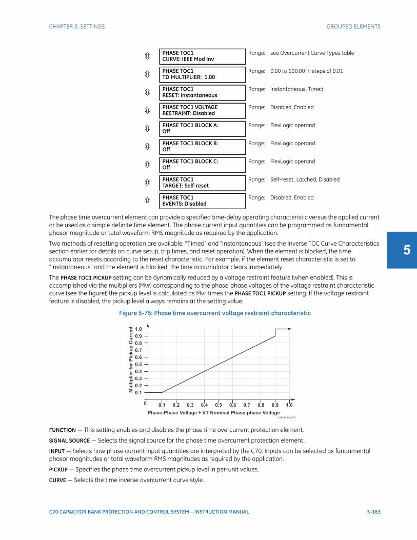
CHAPTER 5: SETTINGS GROUPED ELEMENTS
C70 CAPACITOR BANK PROTECTION AND CONTROL SYSTEM – INSTRUCTION MANUAL 5-163
5
The phase time overcurrent element can provide a specified time-delay operating characteristic versus the applied current or be used as a simple definite time element. The phase current input quantities can be programmed as fundamental phasor magnitude or total waveform RMS magnitude as required by the application.
Two methods of resetting operation are available: “Timed” and “Instantaneous” (see the Inverse TOC Curve Characteristics section earlier for details on curve setup, trip times, and reset operation). When the element is blocked, the time accumulator resets according to the reset characteristic. For example, if the element reset characteristic is set to “Instantaneous” and the element is blocked, the time accumulator clears immediately.
The PHASE TOC1 PICKUP setting can be dynamically reduced by a voltage restraint feature (when enabled). This is accomplished via the multipliers (Mvr) corresponding to the phase-phase voltages of the voltage restraint characteristic curve (see the figure); the pickup level is calculated as Mvr times the PHASE TOC1 PICKUP setting. If the voltage restraint feature is disabled, the pickup level always remains at the setting value.
Figure 5-75: Phase time overcurrent voltage restraint characteristic
FUNCTION — This setting enables and disables the phase time overcurrent protection element.
SIGNAL SOURCE — Selects the signal source for the phase time overcurrent protection element.
INPUT — Selects how phase current input quantities are interpreted by the C70. Inputs can be selected as fundamental phasor magnitudes or total waveform RMS magnitudes as required by the application.
PICKUP — Specifies the phase time overcurrent pickup level in per-unit values.
CURVE — Selects the time inverse overcurrent curve style.
PHASE TOC1CURVE: IEEE Mod Inv
Range: see Overcurrent Curve Types table
PHASE TOC1TD MULTIPLIER: 1.00
Range: 0.00 to 600.00 in steps of 0.01
PHASE TOC1RESET: Instantaneous
Range: Instantaneous, Timed
PHASE TOC1 VOLTAGERESTRAINT: Disabled
Range: Disabled, Enabled
PHASE TOC1 BLOCK A:Off
Range: FlexLogic operand
PHASE TOC1 BLOCK B:Off
Range: FlexLogic operand
PHASE TOC1 BLOCK C:Off
Range: FlexLogic operand
PHASE TOC1TARGET: Self-reset
Range: Self-reset, Latched, Disabled
PHASE TOC1EVENTS: Disabled
Range: Disabled, Enabled
0.1
0.2
0.3
0.4
0.5
0.6
0.7
0.8
0.9
1.0
0.1 0.2 0.3 0.4 0.5 0.6 0.7 0.8 0.9 1.00
818784A4.CDR
Mu
ltip
lie
rfo
rP
ick
up
Cu
rre
nt
Phase-Phase Voltage ÷ VT Nominal Phase-phase Voltage
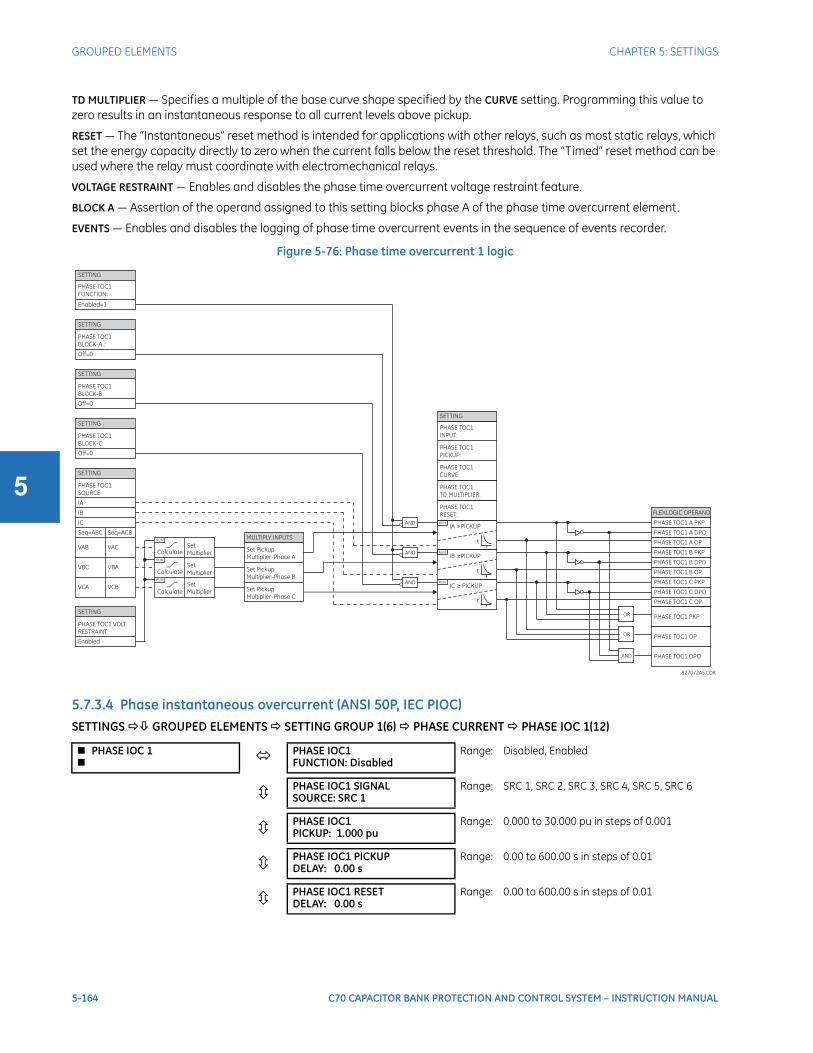
5-164 C70 CAPACITOR BANK PROTECTION AND CONTROL SYSTEM – INSTRUCTION MANUAL
GROUPED ELEMENTS CHAPTER 5: SETTINGS
5
TD MULTIPLIER — Specifies a multiple of the base curve shape specified by the CURVE setting. Programming this value to zero results in an instantaneous response to all current levels above pickup.
RESET — The “Instantaneous” reset method is intended for applications with other relays, such as most static relays, which set the energy capacity directly to zero when the current falls below the reset threshold. The “Timed” reset method can be used where the relay must coordinate with electromechanical relays.
VOLTAGE RESTRAINT — Enables and disables the phase time overcurrent voltage restraint feature.
BLOCK A — Assertion of the operand assigned to this setting blocks phase A of the phase time overcurrent element.
EVENTS — Enables and disables the logging of phase time overcurrent events in the sequence of events recorder.
Figure 5-76: Phase time overcurrent 1 logic
5.7.3.4 Phase instantaneous overcurrent (ANSI 50P, IEC PIOC)SETTINGS GROUPED ELEMENTS SETTING GROUP 1(6) PHASE CURRENT PHASE IOC 1(12)
PHASE IOC 1 PHASE IOC1
FUNCTION: DisabledRange: Disabled, Enabled
PHASE IOC1 SIGNALSOURCE: SRC 1
Range: SRC 1, SRC 2, SRC 3, SRC 4, SRC 5, SRC 6
PHASE IOC1PICKUP: 1.000 pu
Range: 0.000 to 30.000 pu in steps of 0.001
PHASE IOC1 PICKUPDELAY: 0.00 s
Range: 0.00 to 600.00 s in steps of 0.01
PHASE IOC1 RESETDELAY: 0.00 s
Range: 0.00 to 600.00 s in steps of 0.01
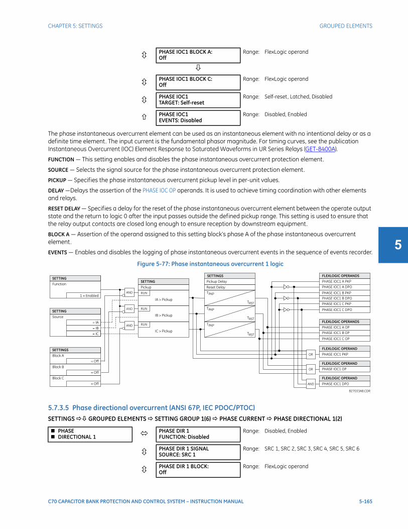
CHAPTER 5: SETTINGS GROUPED ELEMENTS
C70 CAPACITOR BANK PROTECTION AND CONTROL SYSTEM – INSTRUCTION MANUAL 5-165
5
The phase instantaneous overcurrent element can be used as an instantaneous element with no intentional delay or as a definite time element. The input current is the fundamental phasor magnitude. For timing curves, see the publication Instantaneous Overcurrent (IOC) Element Response to Saturated Waveforms in UR Series Relays (GET-8400A).
FUNCTION — This setting enables and disables the phase instantaneous overcurrent protection element.
SOURCE — Selects the signal source for the phase instantaneous overcurrent protection element.
PICKUP — Specifies the phase instantaneous overcurrent pickup level in per-unit values.
DELAY —Delays the assertion of the PHASE IOC OP operands. It is used to achieve timing coordination with other elements and relays.
RESET DELAY — Specifies a delay for the reset of the phase instantaneous overcurrent element between the operate output state and the return to logic 0 after the input passes outside the defined pickup range. This setting is used to ensure that the relay output contacts are closed long enough to ensure reception by downstream equipment.
BLOCK A — Assertion of the operand assigned to this setting block’s phase A of the phase instantaneous overcurrent element.
EVENTS — Enables and disables the logging of phase instantaneous overcurrent events in the sequence of events recorder.
Figure 5-77: Phase instantaneous overcurrent 1 logic
5.7.3.5 Phase directional overcurrent (ANSI 67P, IEC PDOC/PTOC)SETTINGS GROUPED ELEMENTS SETTING GROUP 1(6) PHASE CURRENT PHASE DIRECTIONAL 1(2)
PHASE IOC1 BLOCK A:Off
Range: FlexLogic operand
PHASE IOC1 BLOCK C:Off
Range: FlexLogic operand
PHASE IOC1TARGET: Self-reset
Range: Self-reset, Latched, Disabled
PHASE IOC1EVENTS: Disabled
Range: Disabled, Enabled
PHASE DIRECTIONAL 1 PHASE DIR 1
FUNCTION: DisabledRange: Disabled, Enabled
PHASE DIR 1 SIGNALSOURCE: SRC 1
Range: SRC 1, SRC 2, SRC 3, SRC 4, SRC 5, SRC 6
PHASE DIR 1 BLOCK:Off
Range: FlexLogic operand
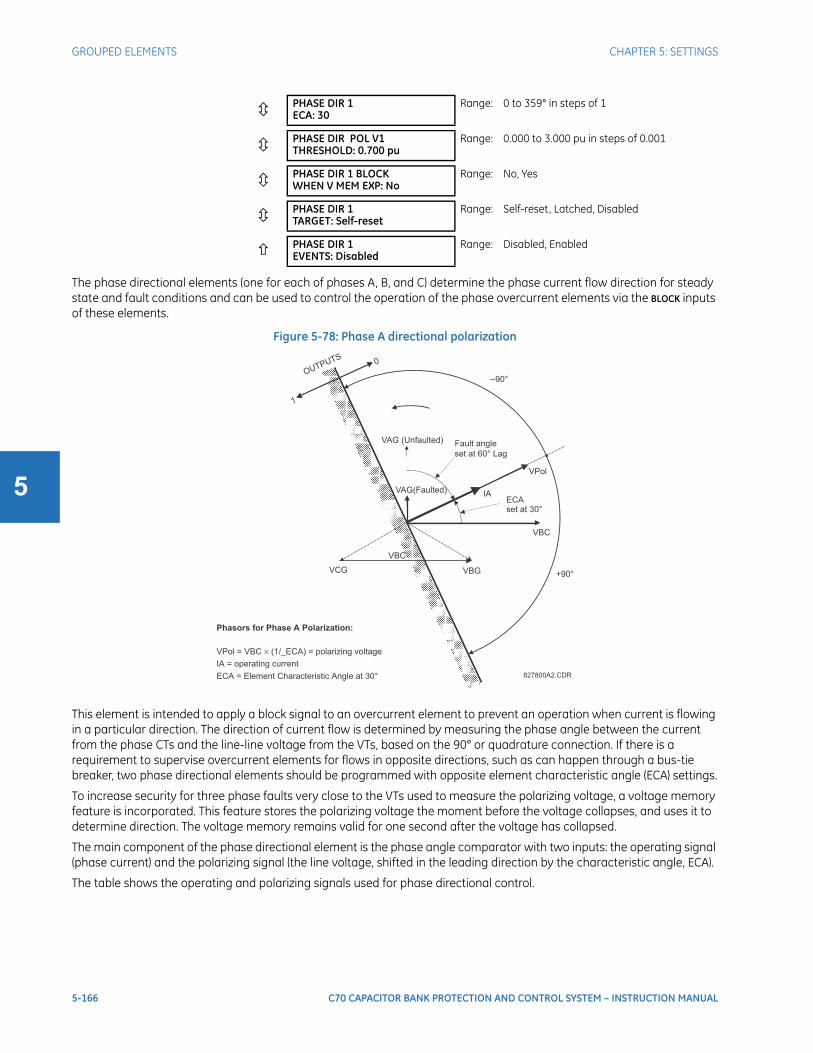
5-166 C70 CAPACITOR BANK PROTECTION AND CONTROL SYSTEM – INSTRUCTION MANUAL
GROUPED ELEMENTS CHAPTER 5: SETTINGS
5
The phase directional elements (one for each of phases A, B, and C) determine the phase current flow direction for steady state and fault conditions and can be used to control the operation of the phase overcurrent elements via the BLOCK inputs of these elements.
Figure 5-78: Phase A directional polarization
This element is intended to apply a block signal to an overcurrent element to prevent an operation when current is flowing in a particular direction. The direction of current flow is determined by measuring the phase angle between the current from the phase CTs and the line-line voltage from the VTs, based on the 90° or quadrature connection. If there is a requirement to supervise overcurrent elements for flows in opposite directions, such as can happen through a bus-tie breaker, two phase directional elements should be programmed with opposite element characteristic angle (ECA) settings.
To increase security for three phase faults very close to the VTs used to measure the polarizing voltage, a voltage memory feature is incorporated. This feature stores the polarizing voltage the moment before the voltage collapses, and uses it to determine direction. The voltage memory remains valid for one second after the voltage has collapsed.
The main component of the phase directional element is the phase angle comparator with two inputs: the operating signal (phase current) and the polarizing signal (the line voltage, shifted in the leading direction by the characteristic angle, ECA).
The table shows the operating and polarizing signals used for phase directional control.
PHASE DIR 1ECA: 30
Range: 0 to 359° in steps of 1
PHASE DIR POL V1THRESHOLD: 0.700 pu
Range: 0.000 to 3.000 pu in steps of 0.001
PHASE DIR 1 BLOCKWHEN V MEM EXP: No
Range: No, Yes
PHASE DIR 1TARGET: Self-reset
Range: Self-reset, Latched, Disabled
PHASE DIR 1EVENTS: Disabled
Range: Disabled, Enabled
827800A2.CDR
VBGVCG
VAG(Faulted) IAECAset at 30°
ECA = Element Characteristic Angle at 30°
IA = operating current
Phasors for Phase A Polarization:
VPol = VBC (1/_ECA) = polarizing voltage×
Fault angle
set at 60° Lag
VAG (Unfaulted)
OUTPUTS0
1
VBC
VBC
VPol
+90°
–90°
CHAPTER 5: SETTINGS GROUPED ELEMENTS
C70 CAPACITOR BANK PROTECTION AND CONTROL SYSTEM – INSTRUCTION MANUAL 5-167
5
Table 5-29: Operating and polarizing signals
Mode of operation• When the function is “Disabled” or the operating current is below 5% × CT nominal, the element output is logic “0”
• When the function is “Enabled,” the operating current is above 5% × CT nominal, and the polarizing voltage is above the PRODUCT SETUP DISPLAY PROPERTIES VOLTAGE CUT-OFF LEVEL value, the element output is dependent on the phase angle between the operating and polarizing signals:
– The element output is logic “0” when the operating current is within polarizing voltage ±90°
– For all other angles, the element output is logic “1”
• Once the voltage memory has expired, the phase overcurrent elements under directional control can be set to block or trip on overcurrent as follows:
– When BLOCK WHEN V MEM EXP is set to “Yes,” the directional element blocks the operation of any phase overcurrent element under directional control when voltage memory expires
– When BLOCK WHEN V MEM EXP is set to “No,” the directional element allows tripping of phase overcurrent elements under directional control when voltage memory expires
In all cases, directional blocking is permitted to resume when the polarizing voltage becomes greater than the polarizing voltage threshold.
SettingsPHASE DIR 1 FUNCTION — This setting enables and disables the phase directional overcurrent protection element.
PHASE DIR 1 SIGNAL SOURCE — This setting is used to select the source for the operating and polarizing signals. The operating current for the phase directional element is the phase current for the selected current source. The polarizing voltage is the line voltage from the phase VTs, based on the 90° or quadrature connection and shifted in the leading direction by the element characteristic angle (ECA).
PHASE DIR 1 BLOCK — Assertion of the operand assigned to this setting blocks operation of the phase directional overcurrent element.
PHASE DIR 1 ECA — This setting specifies the element characteristic angle, that is, the angle by which the polarizing voltage is shifted in the leading direction to achieve dependable operation. In the design of the UR-series elements, a block is applied to an element by asserting logic 1 at the blocking input. Program the phase directional overcurrent element using this setting so that the output is logic 1 for current in the non-tripping direction.
PHASE DIR 1 POL V THRESHOLD — This setting is used to establish the minimum level of voltage for which the phase angle measurement is reliable. The setting is based on VT accuracy.
PHASE DIR 1 BLOCK WHEN V MEM EXP — This setting is used to select the required operation upon expiration of voltage memory. When set to "Yes," the directional element blocks the operation of any phase overcurrent element under directional control, when voltage memory expires. When set to "No," the directional element allows tripping of phase overcurrent elements under directional control.
PHASE DIR 1 EVENTS — This setting enables and disables the logging of phase directional overcurrent events in the sequence of events recorder.
Phase Operating signal Polarizing signal Vpol
ABC phase sequence ACB phase sequence
A angle of IA angle of VBC × (1∠ECA) angle of VCB × (1∠ECA)
B angle of IB angle of VCA × (1∠ECA) angle of VAC × (1∠ECA)
C angle of IC angle of VAB × (1∠ECA) angle of VBA × (1∠ECA)
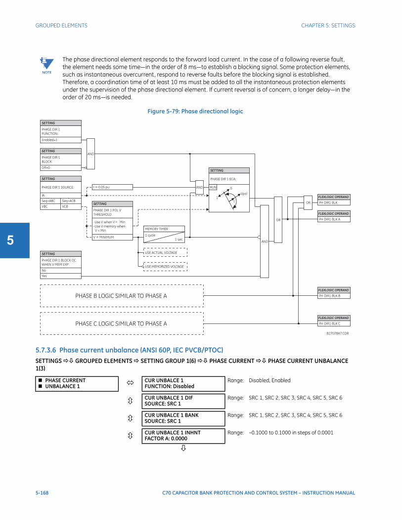
5-168 C70 CAPACITOR BANK PROTECTION AND CONTROL SYSTEM – INSTRUCTION MANUAL
GROUPED ELEMENTS CHAPTER 5: SETTINGS
5
Figure 5-79: Phase directional logic
5.7.3.6 Phase current unbalance (ANSI 60P, IEC PVCB/PTOC)SETTINGS GROUPED ELEMENTS SETTING GROUP 1(6) PHASE CURRENT PHASE CURRENT UNBALANCE 1(3)
NOTE
The phase directional element responds to the forward load current. In the case of a following reverse fault, the element needs some time—in the order of 8 ms—to establish a blocking signal. Some protection elements, such as instantaneous overcurrent, respond to reverse faults before the blocking signal is established. Therefore, a coordination time of at least 10 ms must be added to all the instantaneous protection elements under the supervision of the phase directional element. If current reversal is of concern, a longer delay—in the order of 20 ms—is needed.
PHASE CURRENT UNBALANCE 1 CUR UNBALCE 1
FUNCTION: DisabledRange: Disabled, Enabled
CUR UNBALCE 1 DIFSOURCE: SRC 1
Range: SRC 1, SRC 2, SRC 3, SRC 4, SRC 5, SRC 6
CUR UNBALCE 1 BANKSOURCE: SRC 1
Range: SRC 1, SRC 2, SRC 3, SRC 4, SRC 5, SRC 6
CUR UNBALCE 1 INHNTFACTOR A: 0.0000
Range: –0.1000 to 0.1000 in steps of 0.0001

CHAPTER 5: SETTINGS GROUPED ELEMENTS
C70 CAPACITOR BANK PROTECTION AND CONTROL SYSTEM – INSTRUCTION MANUAL 5-169
5
Up to three identical phase current unbalance elements, one per each CT/VT module configured in hardware, are provided.
CUR UNBALCE 1 INHNTFACTOR C: 0.0000
Range: –0.1000 to 0.1000 in steps of 0.0001
CUR UNBALCE 1 STG 1APICKUP: 0.020 pu
Range: 0.001 to 5.000 pu in steps of 0.001
CUR UNBALCE 1 STG 2APICKUP: 0.030 pu
Range: 0.001 to 5.000 pu in steps of 0.001
CUR UNBALCE 1 STG 3APICKUP: 0.040 pu
Range: 0.001 to 5.000 pu in steps of 0.001
CUR UNBALCE 1 STG 4APICKUP: 0.050 pu
Range: 0.001 to 5.000 pu in steps of 0.001
CUR UNBALCE 1 STG 1BPICKUP: 0.020 pu
Range: 0.001 to 5.000 pu in steps of 0.001
CUR UNBALCE 1 STG 2BPICKUP: 0.030 pu
Range: 0.001 to 5.000 pu in steps of 0.001
CUR UNBALCE 1 STG 3BPICKUP: 0.040 pu
Range: 0.001 to 5.000 pu in steps of 0.001
CUR UNBALCE 1 STG 4BPICKUP: 0.050 pu
Range: 0.001 to 5.000 pu in steps of 0.001
CUR UNBALCE 1 STG 1CPICKUP: 0.020 pu
Range: 0.001 to 5.000 pu in steps of 0.001
CUR UNBALCE 1 STG 2CPICKUP: 0.030 pu
Range: 0.001 to 5.000 pu in steps of 0.001
CUR UNBALCE 1 STG 3CPICKUP: 0.040 pu
Range: 0.001 to 5.000 pu in steps of 0.001
CUR UNBALCE 1 STG 4CPICKUP: 0.050 pu
Range: 0.001 to 5.000 pu in steps of 0.001
CUR UNBALCE 1 STG 1PKP DELAY: 30.00 s
Range: 0.00 to 600.00 s in steps of 0.01
CUR UNBALCE 1 STG 2PKP DELAY: 10.00 s
Range: 0.00 to 600.00 s in steps of 0.01
CUR UNBALCE 1 STG 3PKP DELAY: 1.00 s
Range: 0.00 to 600.00 s in steps of 0.01
CUR UNBALCE 1 STG 4PKP DELAY: 0.20 s
Range: 0.00 to 600.00 s in steps of 0.01
CUR UNBALCE 1DPO DELAY: 0.25 s
Range: 0.00 to 600.00 s in steps of 0.01
CUR UNBL 1 BLK STG1:Off
Range: FlexLogic operand
CUR UNBL 1 BLK STG4:Off
Range: FlexLogic operand
CUR UNBALCE 1TARGET: Self-Reset
Range: Self-reset, Latched, Disabled
CUR UNBALCE 1EVENTS: Disabled
Range: Disabled, Enabled

5-170 C70 CAPACITOR BANK PROTECTION AND CONTROL SYSTEM – INSTRUCTION MANUAL
GROUPED ELEMENTS CHAPTER 5: SETTINGS
5
The element responds to a differential current signal measured via window-type CTs as a vectorial current difference between two parallel banks. With the two capacitors in the same phase identical, the said differential current is zero. Small differences between the capacitors of a given phase result in a small circulating current. Subtracting an adequate portion of the total bank current in a given phase compensates for this inherent unbalance current.
The relay allows manual setting of the inherent unbalance factors, or automatically via the COMMANDS menu. For more information, see the Application of Settings chapter.
Figure 5-80: Phase current unbalance basic connections
The following settings are available for all three elements.
CUR UNBALCE 1 DIF SOURCE — Indicate signal source that signifies the differential currents between the two parallel banks. In order to improve accuracy, a relatively low-ratio window CT can be used for instrumentation. CT primary and secondary ratings are entered under a separate menu. Directionality of wiring these current signals is not important for proper functioning of the feature as long as the sign of the factor compensating for the inherent unbalance is appropriate. For ease of analysis and consistency of relay records, wire all three currents with the same polarity.
CUR UNBALCE 1 BANK SOURCE — Indicate signal source that signifies the total current of the two parallel banks. Either the main CTs are placed in a way ensuring measurement of the total current, or the currents of individual banks are summed externally to the relay by paralleling the main CTs, or summed up internally to the relay using the configuration mechanism of sources. The total bank current is used for compensation for the inherent bank unbalance. CT primary and secondary ratings are entered under a separate menu. Directionality of wiring these current signals is not important for proper functioning of the feature as long as the sign of the factor compensating for the inherent unbalance is appropriate. For ease of analysis and consistency of relay records, wire all three currents with the same polarity. If any of the compensating factors is non-zero, the BANK SOURCE must have phase CT current configured for this function to run.
CUR UNBALCE 1 INHNT FACTOR A(B,C) — This setting specifies the compensating factor for the inherent unbalance between the two banks. Normally, the compensating factors are small numbers being a ratio of the difference between the two impedances, and the sum of the two impedances. For example, with 1% difference between the impedances, the factor is (1-0.99)/(1+0.99) = 0.005. The sign of the compensating factor depends on the polarity of wiring the differential signals, and on which of the two banks has the lower impedance. Quality of balancing the bank with a given value of this setting can be viewed under the ACTUAL VALUES menu. An auto-setting procedure is available under the COMMANDS menu to calculate the compensating factors automatically. Setting the compensating factors to zero effectively disables the compensation and turns this feature into a plain overcurrent element responding to the differential (split phase) currents.
C70 CAPACITOR BANK RELAY
60P
BANK
SOURCE
Phase
CT bank
Grounding method not
relevant, neutral points
must be connected together
DIF
SOURCE
Window / core-
balance CTs
Phase
CT bank
8347516A1.CDR

CHAPTER 5: SETTINGS GROUPED ELEMENTS
C70 CAPACITOR BANK PROTECTION AND CONTROL SYSTEM – INSTRUCTION MANUAL 5-171
5
CUR UNBALCE 1 STG 1A PICKUP to CUR UNBALCE 1 STG 4C PICKUP — These settings specify pickup thresholds for stages 1 through 4 in phases A through C in per-units (pu) of the nominal current of the differential source. A value of 1 pu is the nominal secondary current, or the nominal primary current, respectively, as configured under the differential source of this function.
CUR UNBALCE 1 STG 1 PKP DELAY to CUR UNBALCE 1 STG 4 PKP DELAY — This setting specifies the pickup time delay, individually per each stage of alarming/tripping. Each of the 12 comparators (four stages in three phases) uses an individual timer, but settings for these timers are controlled individually per each stage, not per phase. The timers use a common drop out time delay specified by the next setting.
CUR UNBALCE 1 DPO DELAY — This setting controls a drop-out delay for the operate FlexLogic operands. Individual stages apply individually configurable pickup delays, but use this common drop-out delay.
CUR UNBL 1 BLK STG1 to CUR UNBL 1 BLK STG4 — These settings are used to block the function on a per-stage basis when required. At minimum this function is blocked when the two banks are not paralleled. When unblocked, the function becomes operational after five cycles of intentional delay. High-set instantaneous protection on energization can be provided by a separate instantaneous overcurrent function.
Figure 5-81: Phase current unbalance logic
5.7.4 Neutral current
5.7.4.1 MenuSETTINGS GROUPED ELEMENTS SETTING GROUP 1(6) NEUTRAL CURRENT
NEUTRAL CURRENT NEUTRAL TOC1
See below

5-172 C70 CAPACITOR BANK PROTECTION AND CONTROL SYSTEM – INSTRUCTION MANUAL
GROUPED ELEMENTS CHAPTER 5: SETTINGS
5
The C70 contains protection elements for neutral time overcurrent (ANSI device 51G), neutral instantaneous overcurrent (ANSI device 50G), and neutral current unbalance (ANSI device 60N). A maximum of six ground time overcurrent and 12 ground instantaneous overcurrent elements are available, dependent on the CT/VT modules ordered with the relay. Three neutral current unbalance elements are available.
5.7.4.2 Neutral time overcurrent (ANSI 51N, IEC PTOC)SETTINGS GROUPED ELEMENTS SETTING GROUP 1(6) NEUTRAL CURRENT NEUTRAL TOC1(6)
The neutral time overcurrent element can provide a desired time-delay operating characteristic versus the applied current or be used as a simple definite time element. The neutral current input value is a quantity calculated as 3Io from the phase currents and can be programmed as fundamental phasor magnitude or total waveform RMS magnitude as required by the application.
NEUTRAL TOC6
NEUTRAL IOC1
See page 5-173
NEUTRAL IOC12
NEUTRAL DIRECTIONAL OC1
See page 5-175
NEUTRAL CURRENT UNBALANCE 1
See page 5-179
NEUTRAL CURRENT UNBALANCE 3
NEUTRAL TOC1 NEUTRAL TOC1
FUNCTION: DisabledRange: Disabled, Enabled
NEUTRAL TOC1 SIGNALSOURCE: SRC 1
Range: SRC 1, SRC 2, SRC 3, SRC 4, SRC 5, SRC 6
NEUTRAL TOC1INPUT: Phasor
Range: Phasor, RMS
NEUTRAL TOC1PICKUP: 1.000 pu
Range: 0.000 to 30.000 pu in steps of 0.001
NEUTRAL TOC1CURVE: IEEE Mod Inv
Range: see Overcurrent Curve Types table
NEUTRAL TOC1TD MULTIPLIER: 1.00
Range: 0.00 to 600.00 in steps of 0.01
NEUTRAL TOC1RESET: Instantaneous
Range: Instantaneous, Timed
NEUTRAL TOC1 BLOCK:Off
Range: FlexLogic operand
NEUTRAL TOC1TARGET: Self-reset
Range: Self-reset, Latched, Disabled
NEUTRAL TOC1EVENTS: Disabled
Range: Disabled, Enabled

CHAPTER 5: SETTINGS GROUPED ELEMENTS
C70 CAPACITOR BANK PROTECTION AND CONTROL SYSTEM – INSTRUCTION MANUAL 5-173
5
Two methods of resetting operation are available: “Timed” and “Instantaneous” (see the Inverse TOC Curve Characteristics section for details on curve setup, trip times, and reset operation). When the element is blocked, the time accumulator resets according to the reset characteristic. For example, if the element reset characteristic is set to “Instantaneous” and the element is blocked, the time accumulator clears immediately.
NEUTRAL TOC1 FUNCTION — This setting enables and disables the neutral time overcurrent protection element.
NEUTRAL TOC1 SIGNAL SOURCE — This setting selects the signal source for the neutral time overcurrent protection element.
NEUTRAL TOC1 INPUT — This setting selects how neutral current input quantities are interpreted by the C70. Inputs can be selected as fundamental phasor magnitudes or total waveform RMS magnitudes as required by the application.
NEUTRAL TOC1 PICKUP — This setting specifies the neutral time overcurrent pickup level in per-unit values.
NEUTRAL TOC1 CURVE — This setting selects the inverse time overcurrent curve style.
NEUTRAL TOC1 TD MULTIPLIER — This setting specifies a multiple of the base curve shape specified by the CURVE setting. Programming this value to zero results in an instantaneous response to all current levels above pickup.
NEUTRAL TOC1 RESET — The “Instantaneous” reset method is intended for applications with other relays, such as most static relays, which set the energy capacity directly to zero when the current falls below the reset threshold. The “Timed” reset method can be used where the relay must coordinate with electromechanical relays.
NEUTRAL TOC1 BLOCK — Assertion of the operand assigned to this setting blocks operation of the neutral time overcurrent element.
NEUTRAL TOC1 EVENTS — This setting enables and disables the logging of neutral time overcurrent events in the sequence of events recorder.
Figure 5-82: Neutral time overcurrent 1 logic
5.7.4.3 Neutral instantaneous overcurrent (ANSI 50N, IEC PIOC)SETTINGS GROUPED ELEMENTS SETTING GROUP 1(6) NEUTRAL CURRENT NEUTRAL IOC1(12)
NEUTRAL IOC1 NEUTRAL IOC1
FUNCTION: DisabledRange: Disabled, Enabled
NEUTRAL IOC1 SIGNALSOURCE: SRC 1
Range: SRC 1, SRC 2, SRC 3, SRC 4, SRC 5, SRC 6
NEUTRAL IOC1PICKUP: 1.000 pu
Range: 0.000 to 30.000 pu in steps of 0.001
NEUTRAL IOC1 PICKUPDELAY: 0.00 s
Range: 0.00 to 600.00 s in steps of 0.01
NEUTRAL IOC1 RESETDELAY: 0.00 s
Range: 0.00 to 600.00 s in steps of 0.01
NEUTRAL IOC1 BLOCK:Off
Range: FlexLogic operand
SETTINGNEUTRAL TOC1FUNCTION:Enabled = 1
SETTINGNEUTRAL TOC1SOURCE:IN
NEUTRAL TOC1BLOCK:Off = 0
NEUTRAL TOC1CURVE:NEUTRAL TOC1TD MULTIPLIER:NEUTRAL TOC 1RESET:
SETTINGS
SETTING
IN PICKUP
I
t
NEUTRAL TOC1PICKUP:
RUN
827034A4.VSD
FLEXLOGIC OPERANDS
NEUTRAL TOC1 DPO NEUTRAL TOC1 OP
NEUTRAL TOC1INPUT:
ANDNEUTRAL TOC1 PKP
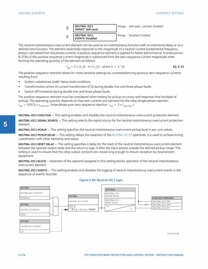
5-174 C70 CAPACITOR BANK PROTECTION AND CONTROL SYSTEM – INSTRUCTION MANUAL
GROUPED ELEMENTS CHAPTER 5: SETTINGS
5
The neutral instantaneous overcurrent element can be used as an instantaneous function with no intentional delay or as a definite time function. The element essentially responds to the magnitude of a neutral current fundamental frequency phasor calculated from the phase currents. A positive-sequence restraint is applied for better performance. A small portion (6.25%) of the positive-sequence current magnitude is subtracted from the zero-sequence current magnitude when forming the operating quantity of the element as follows:
Eq. 5-15
The positive-sequence restraint allows for more sensitive settings by counterbalancing spurious zero-sequence currents resulting from:
• System unbalances under heavy load conditions
• Transformation errors of current transformers (CTs) during double-line and three-phase faults
• Switch-off transients during double-line and three-phase faults
The positive-sequence restraint must be considered when testing for pickup accuracy and response time (multiple of pickup). The operating quantity depends on how test currents are injected into the relay (single-phase injection:
; three-phase pure zero-sequence injection: ).
NEUTRAL IOC1 FUNCTION — This setting enables and disables the neutral instantaneous overcurrent protection element.
NEUTRAL IOC1 SIGNAL SOURCE — This setting selects the signal source for the neutral instantaneous overcurrent protection element.
NEUTRAL IOC1 PICKUP — This setting specifies the neutral instantaneous overcurrent pickup level in per-unit values.
NEUTRAL IOC1 PICKUP DELAY — This setting delays the assertion of the NEUTRAL IOC OP operands. It is used to achieve timing coordination with other elements and relays.
NEUTRAL IOC1 RESET DELAY — This setting specifies a delay for the reset of the neutral instantaneous overcurrent element between the operate output state and the return to logic 0 after the input passes outside the defined pickup range. This setting is used to ensure that the relay output contacts are closed long enough to ensure reception by downstream equipment.
NEUTRAL IOC1 BLOCK — Assertion of the operand assigned to this setting blocks operation of the neutral instantaneous overcurrent element.
NEUTRAL IOC1 EVENTS — This setting enables and disables the logging of neutral instantaneous overcurrent events in the sequence of events recorder.
Figure 5-83: Neutral IOC1 logic
NEUTRAL IOC1TARGET: Self-reset
Range: Self-reset, Latched, Disabled
NEUTRAL IOC1EVENTS: Disabled
Range: Disabled, Enabled
Iop 3 I_0 K I_1×–( )×= where K 1 16⁄=
Iop 0.9375 Iinjected×= Iop 3 Iinjected×=

CHAPTER 5: SETTINGS GROUPED ELEMENTS
C70 CAPACITOR BANK PROTECTION AND CONTROL SYSTEM – INSTRUCTION MANUAL 5-175
5
5.7.4.4 Neutral directional overcurrent (ANSI 67N, IEC PDEF/PTOC)SETTINGS GROUPED ELEMENTS SETTING GROUP 1(6) NEUTRAL CURRENT NEUTRAL DIRECTIONAL OC1
The neutral directional overcurrent element provides both forward and reverse fault direction indications for the NEUTRAL DIR OC1 FWD and NEUTRAL DIR OC1 REV operands, respectively. The output operand is asserted if the magnitude of the operating current is above a pickup level (overcurrent unit) and the fault direction is seen as forward or reverse, respectively (directional unit).
The overcurrent unit responds to the magnitude of a fundamental frequency phasor of either the neutral current calculated from the phase currents or the ground current. There are separate pickup settings for the forward-looking and reverse-looking functions. If set to use the calculated 3I_0, the element applies a positive-sequence restraint for better performance: a small user-programmable portion of the positive-sequence current magnitude is subtracted from the zero-sequence current magnitude when forming the operating quantity.
Eq. 5-16
The positive-sequence restraint allows for more sensitive settings by counterbalancing spurious zero-sequence currents resulting from
• System unbalances under heavy load conditions
• Transformation errors of current transformers (CTs) during double-line and three-phase faults
• Switch-off transients during double-line and three-phase faults
NEUTRAL DIRECTIONAL OC1 NEUTRAL DIR OC1
FUNCTION: DisabledRange: Disabled, Enabled
NEUTRAL DIR OC1SOURCE: SRC 1
Range: SRC 1, SRC 2, SRC 3, SRC 4, SRC 5, SRC 6
NEUTRAL DIR OC1POLARIZING: Voltage
Range: Voltage, Current, Dual, Dual-V, Dual-I
NEUTRAL DIR OC1 POLVOLT: Calculated V0
Range: Calculated V0, Aux. Voltage (VX)
NEUTRAL DIR OC1 OPCURR: Calculated 3I0
Range: Calculated 3I0, Measured IG
NEUTRAL DIR OC1 POS-SEQ RESTRAINT: 0.063
Range: 0.000 to 0.500 in steps of 0.001
NEUTRAL DIR OC1OFFSET: 0.00 Ω
Range: 0.00 to 250.00 Ω in steps of 0.01
NEUTRAL DIR OC1 FWDECA: 75° Lag
Range: –90 to 90° in steps of 1
NEUTRAL DIR OC1 FWDLIMIT ANGLE: 90°
Range: 40 to 90° in steps of 1
NEUTRAL DIR OC1 FWDPICKUP: 0.050 pu
Range: 0.006 to 30.000 pu in steps of 0.001
NEUTRAL DIR OC1 REVLIMIT ANGLE: 90°
Range: 40 to 90° in steps of 1
NEUTRAL DIR OC1 REVPICKUP: 0.050 pu
Range: 0.006 to 30.000 pu in steps of 0.001
NEUTRAL DIR OC1 BLK:Off
Range: FlexLogic operand
NEUTRAL DIR OC1TARGET: Self-reset
Range: Self-reset, Latched, Disabled
NEUTRAL DIR OC1EVENTS: Disabled
Range: Disabled, Enabled
Iop 3 I_0 K I_1×–( )×=
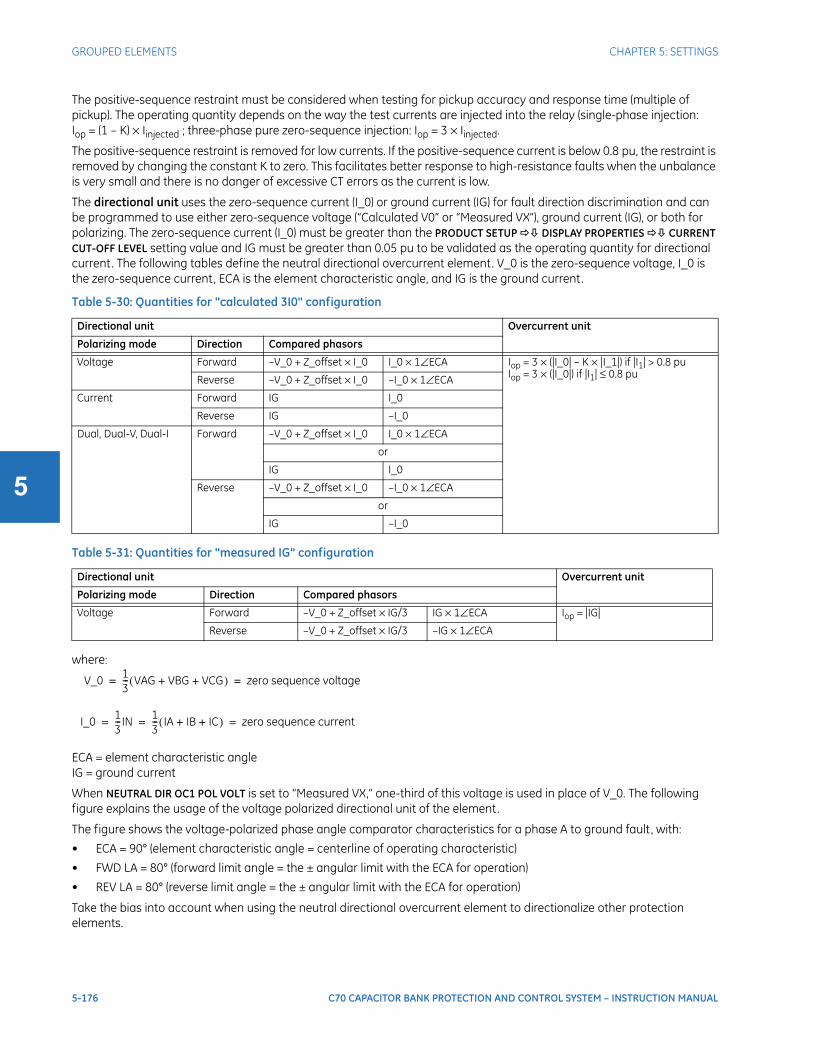
5-176 C70 CAPACITOR BANK PROTECTION AND CONTROL SYSTEM – INSTRUCTION MANUAL
GROUPED ELEMENTS CHAPTER 5: SETTINGS
5
The positive-sequence restraint must be considered when testing for pickup accuracy and response time (multiple of pickup). The operating quantity depends on the way the test currents are injected into the relay (single-phase injection: Iop = (1 – K) × Iinjected ; three-phase pure zero-sequence injection: Iop = 3 × Iinjected.
The positive-sequence restraint is removed for low currents. If the positive-sequence current is below 0.8 pu, the restraint is removed by changing the constant K to zero. This facilitates better response to high-resistance faults when the unbalance is very small and there is no danger of excessive CT errors as the current is low.
The directional unit uses the zero-sequence current (I_0) or ground current (IG) for fault direction discrimination and can be programmed to use either zero-sequence voltage (“Calculated V0” or “Measured VX”), ground current (IG), or both for polarizing. The zero-sequence current (I_0) must be greater than the PRODUCT SETUP DISPLAY PROPERTIES CURRENT CUT-OFF LEVEL setting value and IG must be greater than 0.05 pu to be validated as the operating quantity for directional current. The following tables define the neutral directional overcurrent element. V_0 is the zero-sequence voltage, I_0 is the zero-sequence current, ECA is the element characteristic angle, and IG is the ground current.
Table 5-30: Quantities for "calculated 3I0" configuration
Table 5-31: Quantities for "measured IG" configuration
where:
ECA = element characteristic angleIG = ground current
When NEUTRAL DIR OC1 POL VOLT is set to “Measured VX,” one-third of this voltage is used in place of V_0. The following figure explains the usage of the voltage polarized directional unit of the element.
The figure shows the voltage-polarized phase angle comparator characteristics for a phase A to ground fault, with:
• ECA = 90° (element characteristic angle = centerline of operating characteristic)
• FWD LA = 80° (forward limit angle = the ± angular limit with the ECA for operation)
• REV LA = 80° (reverse limit angle = the ± angular limit with the ECA for operation)
Take the bias into account when using the neutral directional overcurrent element to directionalize other protection elements.
Directional unit Overcurrent unit
Polarizing mode Direction Compared phasors
Voltage Forward –V_0 + Z_offset × I_0 I_0 × 1∠ECA Iop = 3 × (|I_0| – K × |I_1|) if |I1| > 0.8 puIop = 3 × (|I_0|) if |I1| ≤ 0.8 puReverse –V_0 + Z_offset × I_0 –I_0 × 1∠ECA
Current Forward IG I_0
Reverse IG –I_0
Dual, Dual-V, Dual-I Forward –V_0 + Z_offset × I_0 I_0 × 1∠ECA
or
IG I_0
Reverse –V_0 + Z_offset × I_0 –I_0 × 1∠ECA
or
IG –I_0
Directional unit Overcurrent unit
Polarizing mode Direction Compared phasors
Voltage Forward –V_0 + Z_offset × IG/3 IG × 1∠ECA Iop = |IG|
Reverse –V_0 + Z_offset × IG/3 –IG × 1∠ECA
V_0 13--- VAG VBG VCG+ +( ) zero sequence voltage= =
I_0 13--- IN 1
3--- IA IB IC+ +( ) zero sequence current= = =

CHAPTER 5: SETTINGS GROUPED ELEMENTS
C70 CAPACITOR BANK PROTECTION AND CONTROL SYSTEM – INSTRUCTION MANUAL 5-177
5
Figure 5-84: Neutral directional voltage-polarized characteristics
NEUTRAL DIR OC1 POLARIZING — This setting selects the polarizing mode for the directional unit.
• If “Voltage” polarizing is selected, the element uses the zero-sequence voltage angle for polarization. The user can use either the zero-sequence voltage V_0 calculated from the phase voltages, or the zero-sequence voltage supplied externally as the auxiliary voltage V_X, both from the NEUTRAL DIR OC1 SOURCE.
The calculated V_0 can be used as polarizing voltage only if the voltage transformers are connected in Wye. The auxiliary voltage can be used as the polarizing voltage provided SYSTEM SETUP AC INPUTS VOLTAGE BANK AUXILIARY VT CONNECTION is set to “Vn” and the auxiliary voltage is connected to a zero-sequence voltage source (such as broken delta connected secondary of VTs).
The zero-sequence (V_0) or auxiliary voltage (V_X), accordingly, must be greater than the VOLTAGE CUTOFF LEVEL setting specified in the PRODUCT SETUP DISPLAY PROPERTIES menu to be validated for use as a polarizing signal. If the polarizing signal is invalid, neither forward nor reverse indication is given.
• If “Current” polarizing is selected, the element uses the ground current angle connected externally and configured under NEUTRAL OC1 SOURCE for polarization. The ground CT must be connected between the ground and neutral point of an adequate local source of ground current. The ground current must be greater than 0.05 pu to be validated as a polarizing signal. If the polarizing signal is not valid, neither forward nor reverse indication is given. In addition, the zero-sequence current (I_0) must be greater than the PRODUCT SETUP DISPLAY PROPERTIES CURRENT CUT-OFF LEVEL setting value.
For a choice of current polarizing, it is recommended that the polarizing signal be analyzed to ensure that a known direction is maintained irrespective of the fault location. For example, if using an autotransformer neutral current as a polarizing source, ensure that a reversal of the ground current does not occur for a high-side fault. Assume that the low-side system impedance is minimal when checking for this condition. A similar situation arises for a wye/delta/wye transformer, where current in one transformer winding neutral can reverse when faults on both sides of the transformer are considered.
• If “Dual” polarizing is selected, the element performs both directional comparisons as described. A given direction is confirmed if either voltage or current comparators indicate so. If a conflicting (simultaneous forward and reverse) indication occurs, the forward direction overrides the reverse direction.
• If "Dual-V" polarizing is selected, "Voltage" polarizing is performed and "Current" polarizing is ignored if the voltage polarizing signal is valid; otherwise "Current" polarizing is performed if the current polarizing signal is valid. If neither of them is valid, neither forward nor reverse indication is given.
827805A1.CDR
VAG(reference)
VBG
VCG
–3I_0 line
3I_0 line
ECA line
–ECA line
LA
LA
LA
LA
ECA
FWD LAline
FWD OperatingRegion
REV OperatingRegion
FWD LAline
REV LAline
REV LAline
–3V_0 line
3V_0 line

5-178 C70 CAPACITOR BANK PROTECTION AND CONTROL SYSTEM – INSTRUCTION MANUAL
GROUPED ELEMENTS CHAPTER 5: SETTINGS
5
• If "Dual-I" polarizing is selected, "Current" polarizing is performed and "Voltage" polarizing is ignored if the current polarizing signal is valid; otherwise "Voltage" polarizing is performed if the voltage polarizing signal is valid. If neither of them is valid, neither forward nor reverse indication is given.
NEUTRAL DIR OC1 POL VOLT — Selects the polarizing voltage used by the directional unit when "Voltage," "Dual," "Dual-V," or "Dual-I" polarizing mode is set. The polarizing voltage can be programmed to be either the zero-sequence voltage calculated from the phase voltages ("Calculated V0") or supplied externally as an auxiliary voltage ("Measured VX").
NEUTRAL DIR OC1 OP CURR — This setting indicates whether the 3I_0 current calculated from the phase currents, or the ground current is used by this protection. This setting acts as a switch between the neutral and ground modes of operation (ANSI devices 67N and 67G). If set to “Calculated 3I0,” the element uses the phase currents and applies the positive-sequence restraint. If set to “Measured IG,” the element uses ground current supplied to the ground CT of the CT bank configured as NEUTRAL DIR OC1 SOURCE. If this setting is “Measured IG,” then the NEUTRAL DIR OC1 POLARIZING setting must be “Voltage”, as it is not possible to use the ground current as an operating and polarizing signal simultaneously. IG current has to be above 0.05 ps to be used as operate quantity.
NEUTRAL DIR OC1 POS-SEQ RESTRAINT — This setting controls the amount of the positive-sequence restraint. Set it to 0.063 for backward compatibility with firmware revision 3.40 and older. Set it to zero to remove the restraint. Set it higher if large system unbalances or poor CT performance are expected.
NEUTRAL DIR OC1 OFFSET — This setting specifies the offset impedance used by this protection. The primary application for the offset impedance is to guarantee correct identification of fault direction on series compensated lines. In regular applications, the offset impedance ensures proper operation even if the zero-sequence voltage at the relaying point is very small. If this is the intent, the offset impedance is not to be larger than the zero-sequence impedance of the protected circuit. Practically, it shall be several times smaller. Enter the offset impedance in secondary ohms.
NEUTRAL DIR OC1 FWD ECA — This setting defines the characteristic angle (ECA) for the forward direction in the "Voltage" polarizing mode. The "Current" polarizing mode uses a fixed ECA of 0°. The ECA in the reverse direction is the angle set for the forward direction shifted by 180°.
NEUTRAL DIR OC1 FWD LIMIT ANGLE — This setting defines a symmetrical (in both directions from the ECA) limit angle for the forward direction.
NEUTRAL DIR OC1 FWD PICKUP — This setting defines the pickup level for the overcurrent unit of the element in the forward direction. When selecting this setting, keep in mind that the design uses a positive-sequence restraint technique for the “Calculated 3I0” mode of operation.
NEUTRAL DIR OC1 REV LIMIT ANGLE — This setting defines a symmetrical (in both directions from the ECA) limit angle for the reverse direction.
NEUTRAL DIR OC1 REV PICKUP — This setting defines the pickup level for the overcurrent unit of the element in the reverse direction. When selecting this setting, keep in mind that the design uses a positive-sequence restraint technique for the “Calculated 3I0” mode of operation.

CHAPTER 5: SETTINGS GROUPED ELEMENTS
C70 CAPACITOR BANK PROTECTION AND CONTROL SYSTEM – INSTRUCTION MANUAL 5-179
5
Figure 5-85: Neutral directional overcurrent logic
5.7.4.5 Neutral current unbalance (ANSI 60N, IEC PVCB/PTOC)SETTINGS GROUPED ELEMENTS SETTING GROUP 1(6) NEUTRAL CURRENT NEUTRAL CURRENT UNBALANCE 1(3)
NEUTRAL CURRENT UNBALANCE 1 NTRL CUR UNBALCE 1
FUNCTION: DisabledRange: Disabled, Enabled
NTRL CUR UNBALCE 1BANK SOURCE: SRC 1
Range: SRC 1, SRC 2, SRC 3, SRC 4, SRC 5, SRC 6
NTRL CUR UNBALCE 1K MAG: 0.0000
Range: 0.0000 to 0.1500 in steps of 0.0001
NTRL CUR UNBALCE 1K ANG: 0°
Range: 0 to 359° in steps of 1
NTRL CUR UNBALCE 1STG 1 PKP: 0.020 pu
Range: 0.001 to 5.000 pu in steps of 0.001
NTRL CUR UNBALCE 1STG 1 SLOPE: 2.0%
Range: 0.0 to 10.% in steps of 0.1

5-180 C70 CAPACITOR BANK PROTECTION AND CONTROL SYSTEM – INSTRUCTION MANUAL
GROUPED ELEMENTS CHAPTER 5: SETTINGS
5
Up to three identical neutral current unbalance elements, one per each installed CT/VT module.
The neutral current unbalance element responds to a differential current signal measured as a vectorial current difference between neutral currents of parallel banks. In case of ungrounded banks, regular, preferably low-ratio CT can be used. In case of grounded banks, a window or core-balance CT shall be used for increased accuracy/sensitivity.
The function applies simplified compensation for the inherent bank unbalance. Accurate compensation requires three balancing factors that are difficult to measure in practical situations. Instead, a simple and practical compensation responding to both the positive-sequence current and negative-sequence current is applied. This method is easy to apply and remains accurate as long as the zero-sequence bank currents are relatively small. Under large zero-sequence bank currents, the applied method of compensation for the inherent bank unbalance is less accurate. The solution to this problem is to use a small portion of the zero-sequence current at the bank terminals to produce extra restraint and preserve high sensitivity of this protection method.
By setting both the slope and the inherent unbalance compensating factor to zero, one can apply the function as a plain overcurrent element responding to the split-phase neutral current.
The relay allows manual setting of the inherent unbalance factor or automatic setting via a dedicated command. For more information, see the Application of Settings chapter.
NTRL CUR UNBALCE 1STG 2 PKP: 0.030 pu
Range: 0.001 to 5.000 pu in steps of 0.001
NTRL CUR UNBALCE 1STG 2 SLOPE: 2.0%
Range: 0.0 to 10.% in steps of 0.1
NTRL CUR UNBALCE 1STG 3 PKP: 0.040 pu
Range: 0.001 to 5.000 pu in steps of 0.001
NTRL CUR UNBALCE 1STG 3 SLOPE: 2.0%
Range: 0.0 to 10.% in steps of 0.1
NTRL CUR UNBALCE 1STG 4 PKP: 0.050 pu
Range: 0.001 to 5.000 pu in steps of 0.001
NTRL CUR UNBALCE 1STG 4 SLOPE: 5.0%
Range: 0.0 to 10.% in steps of 0.1
NTRL CUR UNBALCE 1STG 1 DEL: 30.00 s
Range: 0.00 to 600.00 s in steps of 0.01
NTRL CUR UNBALCE 1STG 2 DEL: 10.00 s
Range: 0.00 to 600.00 s in steps of 0.01
NTRL CUR UNBALCE 1STG 3 DEL: 1.00 s
Range: 0.00 to 600.00 s in steps of 0.01
NTRL CUR UNBALCE 1STG 4 DEL: 0.20 s
Range: 0.00 to 600.00 s in steps of 0.01
NTRL CUR UNBALCE 1DPO DELAY: 0.25 s
Range: 0.00 to 600.00 s in steps of 0.01
NTRL CUR 1 BLK STG1:Off
Range: FlexLogic operand
NTRL CUR 1 BLK STG2:Off
Range: FlexLogic operand
NTRL CUR 1 BLK STG3:Off
Range: FlexLogic operand
NTRL CUR 1 BLK STG4:Off
Range: FlexLogic operand
NTRL CUR UNBALCE 1TARGET: Self-Reset
Range: Self-reset, Latched, Disabled
NTRL CUR UNBALCE 1EVENTS: Disabled
Range: Disabled, Enabled

CHAPTER 5: SETTINGS GROUPED ELEMENTS
C70 CAPACITOR BANK PROTECTION AND CONTROL SYSTEM – INSTRUCTION MANUAL 5-181
5
Figure 5-86: Neutral current unbalance connections
The following settings are available. They are for the neutral current unbalance 1 element. The same descriptions apply to the neutral current unbalance 2 and 3 elements.
NTRL CUR UNBALCE 1 BANK SOURCE — This setting indicates the signal source that signifies the split-phase neutral current in its ground current channel. At minimum the ground channel of this source must be set. If the factor compensating for inherent bank unbalance is set above zero signalling the intent of using the compensation, the phase currents of this source must be configured as well. Without the phase currents configured under this source, the function would run only if the magnitude of the inherent unbalance factor is set to zero.
To improve accuracy, a relatively low-ratio window CT can be used for instrumentation of the split-phase neutral current, and be wired to a 1 A or even sensitive ground relay input for extra sensitivity. CT primary and secondary ratings are entered under a separate menu. Directionality of wiring of the split-phase current is not important for proper functioning of the feature as long as the angle of the factor compensating for the inherent unbalance is set appropriately.
NTRL CUR UNBALCE 1 K MAG — This setting defines magnitude of the factor compensating for the inherent unbalance of the bank. Under balanced conditions, the amount of the spill current measured in the neutral connection between the banks is proportional to the positive-sequence component of the total current of the two banks. This setting defines the magnitude of the proportionality factor. Quality of balancing the bank with a given value of this setting can be viewed under ACTUAL VALUES menu. An automatic setting procedure is available via the COMMANDS menu to calculate the compensating factor automatically. Setting the compensating factor to zero effectively disables the compensation. If further the slope is set to zero as well, this feature becomes a plain overcurrent element responding to the neutral split-phase current.
NTRL CUR UNBALCE 1 K ANG — This setting defines angle of the factor compensating for the inherent unbalance of the bank. Under balanced conditions, the amount of the spill current measured in the neutral connection between the banks is proportional to the positive-sequence component of the total current of the two banks. This setting defines the angle of
C70 CAPACITOR BANK RELAY
60NBANK
SOURCE
Neutral
CT bank
Ground
CT
Regular, preferably
low-ratio CT for
ungrounded banks
Window / core-
balance CTs for
grounded banks
834735A1.CDR

5-182 C70 CAPACITOR BANK PROTECTION AND CONTROL SYSTEM – INSTRUCTION MANUAL
GROUPED ELEMENTS CHAPTER 5: SETTINGS
5
the proportionality factor. Quality of balancing the bank with a given value of this setting can be viewed under ACTUAL VALUES menu. An automatic setting procedure is available under the COMMANDS menu to calculate the compensating factor automatically.
NTRL CUR UNBALCE 1 STG1 PKP to NTRL CUR UNBALCE 1 STG4 PKP — These settings specify pickup thresholds for stages 1 through 4 in per-units (pu) of the nominal current of the ground current channel of the bank source. A value of 1 pu is the nominal secondary current, or the nominal primary current, respectively, as configured under the bank source of this function.
NTRL CUR UNBALCE 1 STG1 SLOPE to NTRL CUR UNBALCE 1 STG4 SLOPE — These settings specify the slopes for stages 1 through 4. The slope setting is applied if the phase CTs are configured under the bank source. The magnitude of the zero-sequence current is applied as a restraining signal. Typically few percent of slope is enough to ensure security of the function. The factor compensating for the inherent bank unbalance zeroes out the operating signal under relatively balanced bank currents. If the said currents contain a significant zero sequence component, the quality of compensation is lower, hence the need for the restraint, and this slope setting.
NTRL CUR UNBALCE 1 STG1 DEL to NTRL CUR UNBALCE 1 STG4 DEL — This setting specifies the pickup time delay, individually per each stage of alarming/tripping. The timers use a common drop out time delay specified by the next setting.
NTRL CUR UNBALCE 1 DPO DELAY — This setting controls a drop out delay for the operate FlexLogic operands. Individual stages apply individually configurable pickup delays, but use this common drop out delay.
NTRL CUR 1 BLK STG1 to NTRL CUR 1 BLK STG4 — These settings are used to block the function on a per stage basis when required. At minimum this function shall be blocked when the two banks are not paralleled. Note that when unblocked, the function becomes operational after five cycles of intentional delay. High-set instantaneous protection on energization can be provided by a separate instantaneous overcurrent function.
Figure 5-87: Neutral current unbalance logic

CHAPTER 5: SETTINGS GROUPED ELEMENTS
C70 CAPACITOR BANK PROTECTION AND CONTROL SYSTEM – INSTRUCTION MANUAL 5-183
5
5.7.5 Ground current
5.7.5.1 MenuSETTINGS GROUPED ELEMENTS SETTING GROUP 1(6) GROUND CURRENT
5.7.5.2 Ground time overcurrent (ANSI 51G, IEC PTOC)SETTINGS GROUPED ELEMENTS SETTING GROUP 1(6) GROUND CURRENT GROUND TOC1(6)
This element can provide a required time-delay operating characteristic versus the applied current or be used as a simple definite time element. The ground current input value is the quantity measured by the ground input CT and is the fundamental phasor or RMS magnitude. Two methods of resetting operation are available: “Timed” and “Instantaneous” (see the Inverse TOC Curve Characteristics section for details). When the element is blocked, the time accumulator resets according to the reset characteristic. For example, if the element reset characteristic is set to “Instantaneous” and the element is blocked, the time accumulator clears immediately.
GROUND TOC1 FUNCTION — This setting enables and disables the ground time overcurrent protection element.
GROUND TOC1 SIGNAL SOURCE — This setting selects the signal source for the ground time overcurrent protection element.
GROUND TOC1 INPUT — This setting selects how ground current input quantities are interpreted by the C70. Inputs can be selected as fundamental phasor magnitudes or total waveform RMS magnitudes as required by the application.
GROUND CURRENT GROUND TOC1
See below
GROUND TOC6
GROUND IOC1
See page 5-184
GROUND IOC12
GROUND TOC1 GROUND TOC1
FUNCTION: DisabledRange: Disabled, Enabled
GROUND TOC1 SIGNALSOURCE: SRC 1
Range: SRC 1, SRC 2, SRC 3, SRC 4, SRC 5, SRC 6
GROUND TOC1INPUT: Phasor
Range: Phasor, RMS
GROUND TOC1PICKUP: 1.000 pu
Range: 0.000 to 30.000 pu in steps of 0.001
GROUND TOC1CURVE: IEEE Mod Inv
Range: see the Overcurrent Curve Types table
GROUND TOC1TD MULTIPLIER: 1.00
Range: 0.00 to 600.00 in steps of 0.01
GROUND TOC1RESET: Instantaneous
Range: Instantaneous, Timed
GROUND TOC1 BLOCK:Off
Range: FlexLogic operand
GROUND TOC1TARGET: Self-reset
Range: Self-reset, Latched, Disabled
GROUND TOC1EVENTS: Disabled
Range: Disabled, Enabled

5-184 C70 CAPACITOR BANK PROTECTION AND CONTROL SYSTEM – INSTRUCTION MANUAL
GROUPED ELEMENTS CHAPTER 5: SETTINGS
5
GROUND TOC1 PICKUP — This setting specifies the ground time overcurrent pickup level in per-unit values.
GROUND TOC1 CURVE — This setting selects the inverse time overcurrent curve style.
GROUND TOC1 TD MULTIPLIER — This setting specifies a multiple of the base curve shape specified by the CURVE setting. Programming this value to zero results in an instantaneous response to all current levels above pickup.
GROUND TOC1 RESET — The “Instantaneous” reset method is intended for applications with other relays, such as most static relays, which set the energy capacity directly to zero when the current falls below the reset threshold. The “Timed” reset method can be used where the relay must coordinate with electromechanical relays.
GROUND TOC1 BLOCK — Assertion of the operand assigned to this setting blocks operation of the ground time overcurrent element.
GROUND TOC1 EVENTS — This setting enables and disables the logging of ground time overcurrent events in the sequence of events recorder.
Figure 5-88: Ground TOC1 logic
5.7.5.3 Ground instantaneous overcurrent (ANSI 50G, IEC PIOC)SETTINGS GROUPED ELEMENTS SETTING GROUP 1(6) GROUND CURRENT GROUND IOC1(12)
NOTE
These elements measure the current that is connected to the ground channel of a CT/VT module. The conversion range of a standard channel is from 0.02 to 46 times the CT rating.
GROUND IOC1 GROUND IOC1
FUNCTION: DisabledRange: Disabled, Enabled
GROUND IOC1 SIGNALSOURCE: SRC 1
Range: SRC 1, SRC 2, SRC 3, SRC 4, SRC 5, SRC 6
GROUND IOC1PICKUP: 1.000 pu
Range: 0.000 to 30.000 pu in steps of 0.001
GROUND IOC1 PICKUPDELAY: 0.00 s
Range: 0.00 to 600.00 s in steps of 0.01
GROUND IOC1 RESETDELAY: 0.00 s
Range: 0.00 to 600.00 s in steps of 0.01
GROUND IOC1 BLOCK:Off
Range: FlexLogic operand
GROUND IOC1TARGET: Self-reset
Range: Self-reset, Latched, Disabled
GROUND IOC1EVENTS: Disabled
Range: Disabled, Enabled
SETTINGGROUND TOC1FUNCTION:Enabled = 1
SETTINGGROUND TOC1SOURCE:IG
GROUND TOC1BLOCK:Off = 0
FLEXLOGIC OPERANDS
GROUND TOC1 DPO GROUND TOC1 OP
GROUND TOC1CURVE:GROUND TOC1TD MULTIPLIER:GROUND TOC 1RESET:
SETTINGS
SETTING
IG PICKUP
I
t
GROUND TOC1PICKUP:
RUN
827036A4.VSD
GROUND TOC1INPUT:
ANDGROUND TOC1 PKP

CHAPTER 5: SETTINGS GROUPED ELEMENTS
C70 CAPACITOR BANK PROTECTION AND CONTROL SYSTEM – INSTRUCTION MANUAL 5-185
5
The ground instantaneous overcurrent element can be used as an instantaneous element with no intentional delay or as a definite time element. The ground current input is the quantity measured by the ground input CT and is the fundamental phasor magnitude.
Figure 5-89: Ground IOC1 logic
5.7.6 Negative sequence current
5.7.6.1 MenuSETTINGS GROUPED ELEMENTS SETTING GROUP 1(6) NEGATIVE SEQUENCE CURRENT
5.7.6.2 Negative sequence time overcurrent (ANSI 51Q, IEC PTOC)SETTINGS GROUPED ELEMENTS SETTING GROUP 1(6) NEGATIVE SEQUENCE CURRENT NEG SEQ TOC1
NOTE
These elements measure the current that is connected to the ground channel of a CT/VT module. The conversion range of a standard channel is from 0.02 to 46 times the CT rating.
NEGATIVE SEQUENCE CURRENT NEG SEQ TOC1
See below
NEG SEQ TOC2
NEG SEQ IOC1
See page 5-186
NEG SEQ IOC2
NEG SEQ DIR OC1
See page 5-187
NEG SEQ DIR OC2
NEG SEQ TOC1 NEG SEQ TOC1
FUNCTION: DisabledRange: Disabled, Enabled
NEG SEQ TOC1 SIGNALSOURCE: SRC 1
Range: SRC 1, SRC 2, SRC 3, SRC 4, SRC 5, SRC 6
NEG SEQ TOC1PICKUP: 1.000 pu
Range: 0.000 to 30.000 pu in steps of 0.001
NEG SEQ TOC1CURVE: IEEE Mod Inv
Range: see Overcurrent Curve Types table
SETTINGGROUND IOC1FUNCTION:Enabled = 1
SETTINGGROUND IOC1SOURCE:IG
GROUND IOC1BLOCK:Off = 0
FLEXLOGIC OPERANDS
GROUND IOIC DPOGROUND IOC1 OP
SETTING
SETTING
IG PICKUP
GROUND IOC1PICKUP:
RUN
GROUND IOC1 PICKUPDELAY:
SETTINGS
GROUND IOC1 RESETDELAY:
tPKP
tRST
827037A5.VSD
AND
GROUND IOC1 PKP
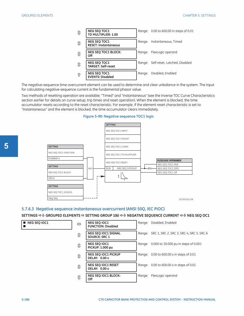
5-186 C70 CAPACITOR BANK PROTECTION AND CONTROL SYSTEM – INSTRUCTION MANUAL
GROUPED ELEMENTS CHAPTER 5: SETTINGS
5
The negative-sequence time overcurrent element can be used to determine and clear unbalance in the system. The input for calculating negative-sequence current is the fundamental phasor value.
Two methods of resetting operation are available; “Timed” and “Instantaneous” (see the Inverse TOC Curve Characteristics section earlier for details on curve setup, trip times and reset operation). When the element is blocked, the time accumulator resets according to the reset characteristic. For example, if the element reset characteristic is set to “Instantaneous” and the element is blocked, the time accumulator clears immediately.
Figure 5-90: Negative sequence TOC1 logic
5.7.6.3 Negative sequence instantaneous overcurrent (ANSI 50Q, IEC PIOC)SETTINGS GROUPED ELEMENTS SETTING GROUP 1(6) NEGATIVE SEQUENCE CURRENT NEG SEQ OC1
NEG SEQ TOC1TD MULTIPLIER: 1.00
Range: 0.00 to 600.00 in steps of 0.01
NEG SEQ TOC1RESET: Instantaneous
Range: Instantaneous, Timed
NEG SEQ TOC1 BLOCK:Off
Range: FlexLogic operand
NEG SEQ TOC1TARGET: Self-reset
Range: Self-reset, Latched, Disabled
NEG SEQ TOC1EVENTS: Disabled
Range: Disabled, Enabled
NEG SEQ IOC1 NEG SEQ IOC1
FUNCTION: DisabledRange: Disabled, Enabled
NEG SEQ IOC1 SIGNALSOURCE: SRC 1
Range: SRC 1, SRC 2, SRC 3, SRC 4, SRC 5, SRC 6
NEG SEQ IOC1PICKUP: 1.000 pu
Range: 0.000 to 30.000 pu in steps of 0.001
NEG SEQ IOC1 PICKUPDELAY: 0.00 s
Range: 0.00 to 600.00 s in steps of 0.01
NEG SEQ IOC1 RESETDELAY: 0.00 s
Range: 0.00 to 600.00 s in steps of 0.01
NEG SEQ IOC1 BLOCK:Off
Range: FlexLogic operand

CHAPTER 5: SETTINGS GROUPED ELEMENTS
C70 CAPACITOR BANK PROTECTION AND CONTROL SYSTEM – INSTRUCTION MANUAL 5-187
5
The negative-sequence instantaneous overcurrent element can be used as an instantaneous function with no intentional delay or as a definite time function. The element responds to the negative-sequence current fundamental frequency phasor magnitude (calculated from the phase currents) and applies a positive-sequence restraint for better performance: a small portion (12.5%) of the positive-sequence current magnitude is subtracted from the negative-sequence current magnitude when forming the operating quantity.
Eq. 5-17
The positive-sequence restraint allows for more sensitive settings by counterbalancing spurious negative-sequence currents resulting from
• System unbalances under heavy load conditions
• Transformation errors of current transformers (CTs) during three-phase faults
• Fault inception and switch-off transients during three-phase faults
The positive-sequence restraint must be considered when testing for pickup accuracy and response time (multiple of pickup). The operating quantity depends on how the test currents are injected into the relay (single-phase injection:
; three-phase injection, opposite rotation: ).
Figure 5-91: Negative sequence IOC1 logic
5.7.6.4 Negative sequence directional overcurrent (ANSI 67Q, IEC PDEF/PTOC)SETTINGS GROUPED ELEMENTS SETTING GROUP 1(6) NEGATIVE SEQUENCE CURRENT NEG SEQ DIR OC1
NEG SEQ IOC1TARGET: Self-reset
Range: Self-reset, Latched, Disabled
NEG SEQ IOC1EVENTS: Disabled
Range: Disabled, Enabled
NEG SEQ DIR OC1 NEG SEQ DIR OC1
FUNCTION: DisabledRange: Disabled, Enabled
NEG SEQ DIR OC1SOURCE: SRC 1
Range: SRC 1, SRC 2, SRC 3, SRC 4, SRC 5, SRC 6
NEG SEQ DIR OC1OFFSET: 0.00 Ω
Range: 0.00 to 250.00 ohms in steps of 0.01
NEG SEQ DIR OC1TYPE: Neg Sequence
Range: Neg Sequence, Zero Sequence
NEG SEQ DIR OC1 POS-SEQ RESTRAINT: 0.063
Range: 0.000 to 0.500 in steps of 0.001
NEG SEQ DIR OC1 FWDECA: 75° Lag
Range: 0 to 90° Lag in steps of 1
Iop I_2 K I_1 where K⋅– 1 8⁄= =
Iop 0.2917 Iinjected⋅= Iop Iinjected=

5-188 C70 CAPACITOR BANK PROTECTION AND CONTROL SYSTEM – INSTRUCTION MANUAL
GROUPED ELEMENTS CHAPTER 5: SETTINGS
5
There are two negative-sequence directional overcurrent protection elements available. The element provides both forward and reverse fault direction indications through its output operands NEG SEQ DIR OC1 FWD and NEG SEQ DIR OC1 REV, respectively. The output operand is asserted if the magnitude of the operating current is above a pickup level (overcurrent unit) and the fault direction is seen as forward or reverse, respectively (directional unit).
The overcurrent unit of the element essentially responds to the magnitude of a fundamental frequency phasor of either the negative-sequence or neutral current as per user selection.
A positive-sequence restraint is applied for better performance: a small user-programmable portion of the positive-sequence current magnitude is subtracted from the negative or zero-sequence current magnitude, respectively, when forming the element operating quantity.
Eq. 5-18
The positive-sequence restraint allows for more sensitive settings by counterbalancing spurious negative-sequence and zero-sequence currents resulting from
• System unbalances under heavy load conditions
• Transformation errors of current transformers (CTs)
• Fault inception and switch-off transients
The positive-sequence restraint must be considered when testing for pickup accuracy and response time (multiple of pickup). The positive-sequence restraint is removed for low currents. If the positive-sequence current is less than 0.8 pu, then the restraint is removed by changing the constant K to zero. This results in better response to high-resistance faults when the unbalance is very small and there is no danger of excessive CT errors, since the current is low.
The operating quantity depends on the way the test currents are injected into the C70. For single phase injection
• Iop = ⅓ × (1 – K) × Iinjected for I_2 mode
• Iop = (1 – K) × Iinjected for I_0 mode if I_1 > 0.8 pu
The directional unit uses the negative-sequence current (I_2) and negative-sequence voltage (V_2).
The following tables define the negative-sequence directional overcurrent element.
Table 5-32: Negative-sequence directional overcurrent unit
Table 5-33: Negative-sequence directional unit
NEG SEQ DIR OC1 FWDLIMIT ANGLE: 90°
Range: 40 to 90° in steps of 1
NEG SEQ DIR OC1 FWDPICKUP: 0.050 pu
Range: 0.015 to 30.000 pu in steps of 0.005
NEG SEQ DIR OC1 REVLIMIT ANGLE: 90°
Range: 40 to 90° in steps of 1
NEG SEQ DIR OC1 REVPICKUP: 0.050 pu
Range: 0.015 to 30.000 pu in steps of 0.005
NEG SEQ DIR OC1 BLK:Off
Range: FlexLogic operand
NEG SEQ DIR OC1TARGET: Self-reset
Range: Self-reset, Latched, Disabled
NEG SEQ DIR OC1EVENTS: Disabled
Range: Disabled, Enabled
Mode Operating current
Negative-sequence Iop = |I_2| – K × I_1|
Zero-sequence Iop = 3 × (|I_0| – K × |I_1|) if |I_1| > 0.8 puIop = 3 × |I_0| if |I_1| ≤ 0.8 pu
Direction Compared phasors
Forward –V_2 + Z_offset × I_2 I_2 × 1∠ECA
Iop I_2 K I_1×–= or Iop 3 I_0 K I_1×–( )×=

CHAPTER 5: SETTINGS GROUPED ELEMENTS
C70 CAPACITOR BANK PROTECTION AND CONTROL SYSTEM – INSTRUCTION MANUAL 5-189
5
The negative-sequence voltage must be greater than the VOLTAGE CUTOFF LEVEL setting specified in the PRODUCT SETUP DISPLAY PROPERTIES menu to be validated for use as a polarizing signal. If the polarizing signal is not validated, neither forward nor reverse indication is given. The following figure explains the usage of the voltage polarized directional unit of the element. It shows the phase angle comparator characteristics for a phase A to ground fault, with settings of
ECA = 75° (element characteristic angle = centerline of operating characteristic)FWD LA = 80° (forward limit angle = ± the angular limit with the ECA for operation)REV LA = 80° (reverse limit angle = ± the angular limit with the ECA for operation)
The element incorporates a current reversal logic: if the reverse direction is indicated for at least 1.25 of a power system cycle, the prospective forward indication is delayed by 1.5 of a power system cycle. The element emulates an electromechanical directional device. Larger operating and polarizing signals result in faster directional discrimination, bringing more security to the element operation.
Figure 5-92: Negative-sequence directional characteristic
The forward-looking function is designed to be more secure compared to the reverse-looking function, so use the forward-looking function for the tripping direction. The reverse-looking function is faster compared to the forward-looking function, so use the reverse-looking function for the blocking direction. This allows for better protection coordination. Take this bias into account when using the negative-sequence directional overcurrent element to directionalize other protection elements. The negative-sequence directional pickup must be greater than the PRODUCT SETUP DISPLAY PROPERTIES CURRENT CUT-OFF LEVEL setting value.
SettingsNEG SEQ DIR OC1 OFFSET — Specifies the offset impedance used by this protection. The primary application for the offset impedance is to guarantee correct identification of fault direction on series compensated lines (see the Application of Settings chapter for information on how to calculate this setting). In regular applications, the offset impedance ensures
Reverse –V_2 + Z_offset × I_2 –(I_2 × 1∠ECA)
Forward –V_2 + Z_offset × I_2 I_2 × 1∠ECA
Reverse –V_2 + Z_offset × I_2 –(I_2 × 1∠ECA)
Direction Compared phasors
827806A2.CDR
VAG (reference)
VCG VBG
–I_2 line
I_2 line
ECA line
–ECA line
LA
LA
LA
LA ECA
FWD OperatingRegion
REV OperatingRegion
FWDLA
FWDLA
REVLA
REVLA
V_2 line
–V_2 line

5-190 C70 CAPACITOR BANK PROTECTION AND CONTROL SYSTEM – INSTRUCTION MANUAL
GROUPED ELEMENTS CHAPTER 5: SETTINGS
5
proper operation even if the negative-sequence voltage at the relaying point is very small. If this is the intent, the offset impedance shall not be larger than the negative-sequence impedance of the protected circuit. Practically, it is several times smaller. Enter the offset impedance in secondary ohms.
NEG SEQ DIR OC1 TYPE — Selects the operating mode for the overcurrent unit of the element. The choices are “Neg Sequence” and “Zero Sequence.” In some applications it is advantageous to use a directional negative-sequence overcurrent function instead of a directional zero-sequence overcurrent function as inter-circuit mutual effects are minimized.
NEG SEQ DIR OC1 POS-SEQ RESTRAINT — Controls the positive-sequence restraint. Set it to 0.063 (in “Zero Sequence” mode) or 0.125 (in “Neg Sequence” mode) for backward compatibility with revisions 3.40 and earlier. Set it to zero to remove the restraint. Set it higher if large system unbalances or poor CT performance are expected.
NEG SEQ DIR OC1 FWD ECA — Select the element characteristic angle (ECA) for the forward direction. The element characteristic angle in the reverse direction is the angle set for the forward direction shifted by 180°.
NEG SEQ DIR OC1 FWD LIMIT ANGLE — Defines a symmetrical limit angle (in both directions from the ECA) for the forward direction.
NEG SEQ DIR OC1 FWD PICKUP — Defines the pickup level for the overcurrent unit in the forward direction. This pickup threshold applies to zero-sequence or negative-sequence current based on the NEG SEQ DIR OC1 TYPE setting. When specifying this setting, keep in mind that the design uses a positive-sequence restraint technique.
NEG SEQ DIR OC1 REV LIMIT ANGLE — Defines a symmetrical limit angle (in both directions from the ECA) for the reverse direction.
NEG SEQ DIR OC1 REV PICKUP — Defines the pickup level for the overcurrent unit in the reverse direction. This pickup threshold applies to zero-sequence or negative-sequence current based on the NEG SEQ DIR OC1 TYPE setting. When selecting this setting, keep in mind that the design uses a positive-sequence restraint technique.
Figure 5-93: Negative-sequence directional OC1 logic
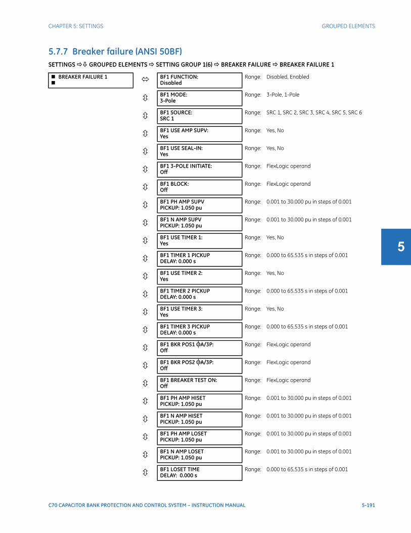
CHAPTER 5: SETTINGS GROUPED ELEMENTS
C70 CAPACITOR BANK PROTECTION AND CONTROL SYSTEM – INSTRUCTION MANUAL 5-191
5
5.7.7 Breaker failure (ANSI 50BF)SETTINGS GROUPED ELEMENTS SETTING GROUP 1(6) BREAKER FAILURE BREAKER FAILURE 1
BREAKER FAILURE 1 BF1 FUNCTION:
DisabledRange: Disabled, Enabled
BF1 MODE:3-Pole
Range: 3-Pole, 1-Pole
BF1 SOURCE:SRC 1
Range: SRC 1, SRC 2, SRC 3, SRC 4, SRC 5, SRC 6
BF1 USE AMP SUPV:Yes
Range: Yes, No
BF1 USE SEAL-IN:Yes
Range: Yes, No
BF1 3-POLE INITIATE:Off
Range: FlexLogic operand
BF1 BLOCK:Off
Range: FlexLogic operand
BF1 PH AMP SUPVPICKUP: 1.050 pu
Range: 0.001 to 30.000 pu in steps of 0.001
BF1 N AMP SUPVPICKUP: 1.050 pu
Range: 0.001 to 30.000 pu in steps of 0.001
BF1 USE TIMER 1:Yes
Range: Yes, No
BF1 TIMER 1 PICKUPDELAY: 0.000 s
Range: 0.000 to 65.535 s in steps of 0.001
BF1 USE TIMER 2:Yes
Range: Yes, No
BF1 TIMER 2 PICKUPDELAY: 0.000 s
Range: 0.000 to 65.535 s in steps of 0.001
BF1 USE TIMER 3:Yes
Range: Yes, No
BF1 TIMER 3 PICKUPDELAY: 0.000 s
Range: 0.000 to 65.535 s in steps of 0.001
BF1 BKR POS1 φA/3P:Off
Range: FlexLogic operand
BF1 BKR POS2 φA/3P:Off
Range: FlexLogic operand
BF1 BREAKER TEST ON:Off
Range: FlexLogic operand
BF1 PH AMP HISETPICKUP: 1.050 pu
Range: 0.001 to 30.000 pu in steps of 0.001
BF1 N AMP HISETPICKUP: 1.050 pu
Range: 0.001 to 30.000 pu in steps of 0.001
BF1 PH AMP LOSETPICKUP: 1.050 pu
Range: 0.001 to 30.000 pu in steps of 0.001
BF1 N AMP LOSETPICKUP: 1.050 pu
Range: 0.001 to 30.000 pu in steps of 0.001
BF1 LOSET TIMEDELAY: 0.000 s
Range: 0.000 to 65.535 s in steps of 0.001

5-192 C70 CAPACITOR BANK PROTECTION AND CONTROL SYSTEM – INSTRUCTION MANUAL
GROUPED ELEMENTS CHAPTER 5: SETTINGS
5In general, a breaker failure scheme determines that a breaker signaled to trip has not cleared a fault within a definite time, so further tripping action must be performed. Tripping from the breaker failure scheme should trip all breakers, both local and remote, that can supply current to the faulted zone. Usually operation of a breaker failure element causes clearing of a larger section of the power system than the initial trip. Because breaker failure can result in tripping a large number of breakers and this affects system safety and stability, a very high level of security is required.
Two schemes are provided: one for three-pole tripping only (identified by the name “3BF”) and one for three pole plus single-pole operation (identified by the name “1BF”). The philosophy used in these schemes is identical. The operation of a breaker failure element includes three stages: initiation, determination of a breaker failure condition, and output.
Initiation stageA FlexLogic operand representing the protection trip signal initially sent to the breaker must be selected to initiate the scheme. The initiating signal is sealed-in if primary fault detection can reset before the breaker failure timers have finished timing. The seal-in is supervised by current level, so it is reset when the fault is cleared. If desired, an incomplete sequence seal-in reset can be implemented by using the initiating operand to also initiate a FlexLogic timer, set longer than any breaker failure timer, whose output operand is selected to block the breaker failure scheme.
Schemes can be initiated either directly or with current level supervision. It is particularly important in any application to decide if a current-supervised initiate is to be used. The use of a current-supervised initiate results in the breaker failure element not being initiated for a breaker that has very little or no current flowing through it, which can be the case for transformer faults. For those situations where it is required to maintain breaker fail coverage for fault levels below the BF1 PH AMP SUPV PICKUP or the BF1 N AMP SUPV PICKUP setting, do not use a current supervised initiate. Utilize this feature for those situations where coordinating margins can be reduced when high speed reclosing is used. Thus, if this choice is made, fault levels must always be above the supervision pickup levels for dependable operation of the breaker fail scheme. This can also occur in breaker-and-a-half or ring bus configurations where the first breaker closes into a fault; the protection trips and attempts to initiate breaker failure for the second breaker, which is in the process of closing, but does not yet have current flowing through it.
When the scheme is initiated, it immediately sends a trip signal to the breaker initially signaled to trip (this feature is usually described as re-trip). This reduces the possibility of widespread tripping that results from a declaration of a failed breaker.
BF1 TRIP DROPOUTDELAY: 0.000 s
Range: 0.000 to 65.535 s in steps of 0.001
BF1 TARGET:Self-Reset
Range: Self-reset, Latched, Disabled
BF1 EVENTS:Disabled
Range: Disabled, Enabled
BF1 PH A INITIATE:Off
Range: FlexLogic operandValid only for 1-Pole breaker failure schemes
BF1 PH B INITIATE:Off
Range: FlexLogic operandValid only for 1-Pole breaker failure schemes
BF1 PH C INITIATE:Off
Range: FlexLogic operandValid only for 1-Pole breaker failure schemes
BF1 BKR POS1 φB:Off
Range: FlexLogic operandValid only for 1-Pole breaker failure schemes
BF1 BKR POS1 φC:Off
Range: FlexLogic operandValid only for 1-Pole breaker failure schemes
BF1 BKR POS2 φB:Off
Range: FlexLogic operandValid only for 1-Pole breaker failure schemes
BF1 BKR POS2 φC:Off
Range: FlexLogic operandValid only for 1-Pole breaker failure schemes

CHAPTER 5: SETTINGS GROUPED ELEMENTS
C70 CAPACITOR BANK PROTECTION AND CONTROL SYSTEM – INSTRUCTION MANUAL 5-193
5
Determination of a breaker failure conditionThe schemes determine a breaker failure condition via three paths. Each of these paths is equipped with a time delay, after which a failed breaker is declared and trip signals are sent to all breakers required to clear the zone. The delayed paths are associated with breaker failure timers 1, 2, and 3, which are intended to have delays increasing with increasing timer numbers. These delayed paths are individually enabled to allow for maximum flexibility.
Timer 1 logic (early path) is supervised by a fast-operating breaker auxiliary contact. If the breaker is still closed (as indicated by the auxiliary contact) and fault current is detected after the delay interval, an output is issued. Operation of the breaker auxiliary switch indicates that the breaker has mechanically operated. The continued presence of current indicates that the breaker has failed to interrupt the circuit.
Timer 2 logic (main path) is not supervised by a breaker auxiliary contact. If fault current is detected after the delay interval, an output is issued. This path is intended to detect a breaker that opens mechanically but fails to interrupt fault current; the logic therefore does not use a breaker auxiliary contact.
The timer 1 and 2 paths provide two levels of current supervision, high-set and low-set, that allow the supervision level to change from a current which flows before a breaker inserts an opening resistor into the faulted circuit to a lower level after resistor insertion. The high-set detector is enabled after timeout of timer 1 or 2, along with a timer that enables the low-set detector after its delay interval. The delay interval between high-set and low-set is the expected breaker opening time. Both current detectors provide a fast operating time for currents at small multiples of the pickup value. The overcurrent detectors are required to operate after the breaker failure delay interval to eliminate the need for very fast resetting overcurrent detectors.
Timer 3 logic (slow path) is supervised by a breaker auxiliary contact and a control switch contact used to indicate that the breaker is in or out-of-service, disabling this path when the breaker is out-of-service for maintenance. There is no current level check in this logic as it is intended to detect low magnitude faults and it is therefore the slowest to operate.
OutputThe outputs from the schemes are:
• FlexLogic operands that report on the operation of portions of the scheme
• FlexLogic operand used to re-trip the protected breaker
• FlexLogic operands that initiate tripping required to clear the faulted zone. The trip output can be sealed-in for an adjustable period.
• Target message indicating a failed breaker has been declared
• Illumination of the faceplate Trip LED (and the Phase A, B, or C LED, if applicable)
Main path sequence
Figure 5-94: Breaker failure main path sequence
The current supervision elements reset in less than 0.7 of a power cycle for any multiple of pickup current as shown in the following figure.
PROTECTION OPERATION BREAKER INTERRUPTING TIME
CALCULATED CURRENT MAGNITUDE
ACTUAL CURRENT MAGNITUDEFAILED INTERRUPTION
CORRECT INTERRUPTION
Rampdown
(ASSUMED 1.5 cycles)
INITIATE (1/8 cycle)BREAKER FAILURE TIMER No. 2 (±1/8 cycle)
BREAKER FAILURE CURRENT DETECTOR PICKUP (1/8 cycle)
BREAKER FAILURE OUTPUT RELAY PICKUP (1/4 cycle)
FAULTOCCURS
1 2 3 4 5 6 7 8 9 10 110
0
0
AMP
(ASSUMED 3 cycles)
cycles
827083A6.CDR
MARGIN(Assumed 2 Cycles)
BACKUP BREAKER OPERATING TIME(Assumed 3 Cycles)

5-194 C70 CAPACITOR BANK PROTECTION AND CONTROL SYSTEM – INSTRUCTION MANUAL
GROUPED ELEMENTS CHAPTER 5: SETTINGS
5
Figure 5-95: Breaker failure overcurrent supervision reset time
SettingsBF1 MODE — This setting is used to select the breaker failure operating mode: single or three pole.
BF1 USE AMP SUPV — If set to "Yes," the element is initiated if current flowing through the breaker is above the supervision pickup level.
BF1 USE SEAL-IN — If set to "Yes," the element is sealed-in if current flowing through the breaker is above the supervision pickup level.
BF1 3-POLE INITIATE — This setting selects the FlexLogic operand that initiates three-pole tripping of the breaker.
BF1 PH AMP SUPV PICKUP — This setting is used to set the phase current initiation and seal-in supervision level. Generally this setting detects the lowest expected fault current on the protected breaker. It can be set as low as necessary (lower than breaker resistor current or lower than load current)—high-set and low-set current supervision guarantee correct operation.
BF1 N AMP SUPV PICKUP — This setting is used to set the neutral current initiate and seal-in supervision level. Generally this setting detects the lowest expected fault current on the protected breaker. Neutral current supervision is used only in the three phase scheme to provide increased sensitivity. This setting is valid only for three-pole tripping schemes.
BF1 USE TIMER 1 — If set to "Yes," the early path is operational.
BF1 TIMER 1 PICKUP DELAY — Timer 1 is set to the shortest time required for breaker auxiliary contact Status-1 to open, from the time the initial trip signal is applied to the breaker trip circuit, plus a safety margin.
BF1 USE TIMER 2 — If set to "Yes," the main path is operational.
BF1 TIMER 2 PICKUP DELAY — Timer 2 is set to the expected opening time of the breaker, plus a safety margin. This safety margin was historically intended to allow for measuring and timing errors in the breaker failure scheme equipment. In microprocessor relays this time is not significant. In C70 relays, which use a Fourier transform, the calculated current magnitude ramps-down to zero one power frequency cycle after the current is interrupted, and this lag needs to be included in the overall margin duration, as it occurs after current interruption. The Breaker Failure Main Path Sequence figure that follows shows a margin of two cycles; this interval is considered the minimum appropriate for most applications.
Note that in bulk oil circuit breakers, the interrupting time for currents less than 25% of the interrupting rating can be significantly longer than the normal interrupting time.
BF1 USE TIMER 3 — If set to "Yes," the Slow Path is operational.
BF1 TIMER 3 PICKUP DELAY — Timer 3 is set to the same interval as timer 2, plus an increased safety margin. Because this path is intended to operate only for low level faults, the delay can be in the order of 300 to 500 ms.
836769A4.CDR
0
0.2
0.4
0.6
0.8
0 20 40 60 80 100 120 140
Average
Maximum
Margin
Mul ple of pickupfault current
threshold setting
Bre
ake
rfa
ilu
rere
se
tti
me
(cy
cle
s)
CHAPTER 5: SETTINGS GROUPED ELEMENTS
C70 CAPACITOR BANK PROTECTION AND CONTROL SYSTEM – INSTRUCTION MANUAL 5-195
5
BF1 BKR POS1 φA/3P — This setting selects the FlexLogic operand that represents the protected breaker early-type auxiliary switch contact (52/a). When using the single-pole breaker failure scheme, this operand represents the protected breaker early-type auxiliary switch contact on pole A. This is normally a non-multiplied form-A contact. The contact can even be adjusted to have the shortest possible operating time.
BF1 BKR POS2 φA/3P — This setting selects the FlexLogic operand that represents the breaker normal-type auxiliary switch contact (52/a). When using the single-pole breaker failure scheme, this operand represents the protected breaker auxiliary switch contact on pole A. This can be a multiplied contact.
BF1 BREAKER TEST ON — This setting is used to select the FlexLogic operand that represents the breaker in-service/out-of-service switch set to the out-of-service position.
BF1 PH AMP HISET PICKUP — This setting sets the phase current output supervision level. Generally this setting is to detect the lowest expected fault current on the protected breaker, before a breaker opening resistor is inserted.
BF1 N AMP HISET PICKUP — This setting sets the neutral current output supervision level. Generally this setting is to detect the lowest expected fault current on the protected breaker, before a breaker opening resistor is inserted. Neutral current supervision is used only in the three pole scheme to provide increased sensitivity. This setting is valid only for three-pole breaker failure schemes.
BF1 PH AMP LOSET PICKUP — This setting sets the phase current output supervision level. Generally this setting is to detect the lowest expected fault current on the protected breaker, after a breaker opening resistor is inserted (approximately 90% of the resistor current).
BF1 N AMP LOSET PICKUP — This setting sets the neutral current output supervision level. Generally this setting is to detect the lowest expected fault current on the protected breaker, after a breaker opening resistor is inserted (approximately 90% of the resistor current). This setting is valid only for three-pole breaker failure schemes.
BF1 LOSET TIME DELAY — Sets the pickup delay for current detection after opening resistor insertion.
BF1 TRIP DROPOUT DELAY — This setting is used to set the period of time for which the trip output is sealed-in. This timer must be coordinated with the automatic reclosing scheme of the failed breaker, to which the breaker failure element sends a cancel reclosure signal. Reclosure of a remote breaker can also be prevented by holding a transfer trip signal on longer than the reclaim time.
BF1 PH A INITIATE / BF1 PH B INITIATE / BF 1 PH C INITIATE — These settings select the FlexLogic operand to initiate phase A, B, or C single-pole tripping of the breaker and the phase A, B, or C portion of the scheme, accordingly. This setting is only valid for single-pole breaker failure schemes.
BF1 BKR POS1 φB / BF1 BKR POS 1 φC — These settings select the FlexLogic operand to represents the protected breaker early-type auxiliary switch contact on poles B or C, accordingly. This contact is normally a non-multiplied Form-A contact. The contact can even be adjusted to have the shortest possible operating time. This setting is valid only for single-pole breaker failure schemes.
BF1 BKR POS2 φB — Selects the FlexLogic operand that represents the protected breaker normal-type auxiliary switch contact on pole B (52/a). This can be a multiplied contact. This setting is valid only for single-pole breaker failure schemes.
BF1 BKR POS2 φC — This setting selects the FlexLogic operand that represents the protected breaker normal-type auxiliary switch contact on pole C (52/a). This can be a multiplied contact. For single-pole operation, the scheme has the same overall general concept except that it provides re-tripping of each single pole of the protected breaker. The approach shown in the following single pole tripping diagram uses the initiating information to determine which pole is supposed to trip. The logic is segregated on a per-pole basis. The overcurrent detectors have ganged settings. This setting is valid only for single-pole breaker failure schemes.
Upon operation of the breaker failure element for a single pole trip command, a three-pole trip command needs to be given via output operand BKR FAIL 1 TRIP OP.
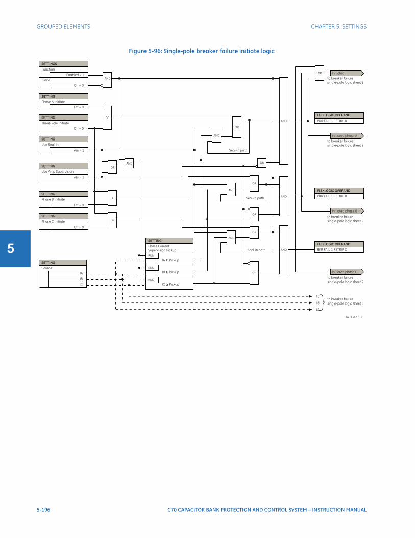
5-196 C70 CAPACITOR BANK PROTECTION AND CONTROL SYSTEM – INSTRUCTION MANUAL
GROUPED ELEMENTS CHAPTER 5: SETTINGS
5
Figure 5-96: Single-pole breaker failure initiate logic

CHAPTER 5: SETTINGS GROUPED ELEMENTS
C70 CAPACITOR BANK PROTECTION AND CONTROL SYSTEM – INSTRUCTION MANUAL 5-197
5
Figure 5-97: Single-pole breaker failure, timers logic
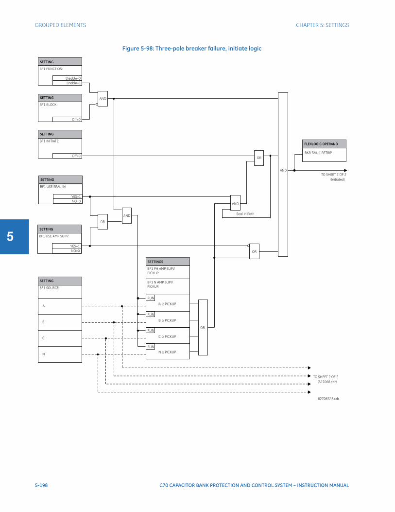
5-198 C70 CAPACITOR BANK PROTECTION AND CONTROL SYSTEM – INSTRUCTION MANUAL
GROUPED ELEMENTS CHAPTER 5: SETTINGS
5
Figure 5-98: Three-pole breaker failure, initiate logic

CHAPTER 5: SETTINGS GROUPED ELEMENTS
C70 CAPACITOR BANK PROTECTION AND CONTROL SYSTEM – INSTRUCTION MANUAL 5-199
5
Figure 5-99: Three-pole breaker failure, timers logic
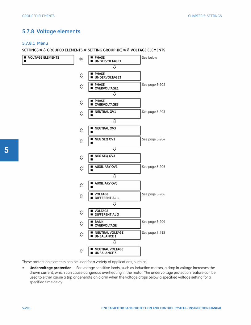
5-200 C70 CAPACITOR BANK PROTECTION AND CONTROL SYSTEM – INSTRUCTION MANUAL
GROUPED ELEMENTS CHAPTER 5: SETTINGS
5
5.7.8 Voltage elements
5.7.8.1 MenuSETTINGS GROUPED ELEMENTS SETTING GROUP 1(6) VOLTAGE ELEMENTS
These protection elements can be used for a variety of applications, such as
• Undervoltage protection — For voltage sensitive loads, such as induction motors, a drop in voltage increases the drawn current, which can cause dangerous overheating in the motor. The undervoltage protection feature can be used to either cause a trip or generate an alarm when the voltage drops below a specified voltage setting for a specified time delay.
VOLTAGE ELEMENTS PHASE
UNDERVOLTAGE1See below
PHASE UNDERVOLTAGE3
PHASE OVERVOLTAGE1
See page 5-202
PHASE OVERVOLTAGE3
NEUTRAL OV1
See page 5-203
NEUTRAL OV3
NEG SEQ OV1
See page 5-204
NEG SEQ OV3
AUXILIARY OV1
See page 5-205
AUXILIARY OV3
VOLTAGE DIFFERENTIAL 1
See page 5-206
VOLTAGE DIFFERENTIAL 3
BANK OVERVOLTAGE
See page 5-209
NEUTRAL VOLTAGE UNBALANCE 1
See page 5-213
NEUTRAL VOLTAGE UNBALANCE 3
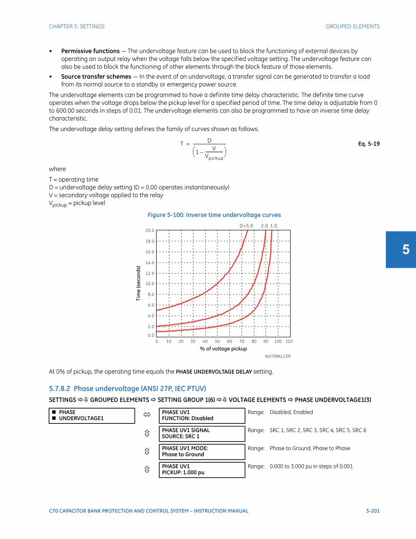
CHAPTER 5: SETTINGS GROUPED ELEMENTS
C70 CAPACITOR BANK PROTECTION AND CONTROL SYSTEM – INSTRUCTION MANUAL 5-201
5
• Permissive functions — The undervoltage feature can be used to block the functioning of external devices by operating an output relay when the voltage falls below the specified voltage setting. The undervoltage feature can also be used to block the functioning of other elements through the block feature of those elements.
• Source transfer schemes — In the event of an undervoltage, a transfer signal can be generated to transfer a load from its normal source to a standby or emergency power source.
The undervoltage elements can be programmed to have a definite time delay characteristic. The definite time curve operates when the voltage drops below the pickup level for a specified period of time. The time delay is adjustable from 0 to 600.00 seconds in steps of 0.01. The undervoltage elements can also be programmed to have an inverse time delay characteristic.
The undervoltage delay setting defines the family of curves shown as follows.
Eq. 5-19
where
T = operating timeD = undervoltage delay setting (D = 0.00 operates instantaneously)V = secondary voltage applied to the relayVpickup = pickup level
Figure 5-100: Inverse time undervoltage curves
At 0% of pickup, the operating time equals the PHASE UNDERVOLTAGE DELAY setting.
5.7.8.2 Phase undervoltage (ANSI 27P, IEC PTUV)SETTINGS GROUPED ELEMENTS SETTING GROUP 1(6) VOLTAGE ELEMENTS PHASE UNDERVOLTAGE1(3)
PHASE UNDERVOLTAGE1 PHASE UV1
FUNCTION: DisabledRange: Disabled, Enabled
PHASE UV1 SIGNALSOURCE: SRC 1
Range: SRC 1, SRC 2, SRC 3, SRC 4, SRC 5, SRC 6
PHASE UV1 MODE:Phase to Ground
Range: Phase to Ground, Phase to Phase
PHASE UV1PICKUP: 1.000 pu
Range: 0.000 to 3.000 pu in steps of 0.001
T D
1 VVpickup----------------–
------------------------------=
842788A1.CDR
% of voltage pickup
Tim
e(s
ec
on
ds)
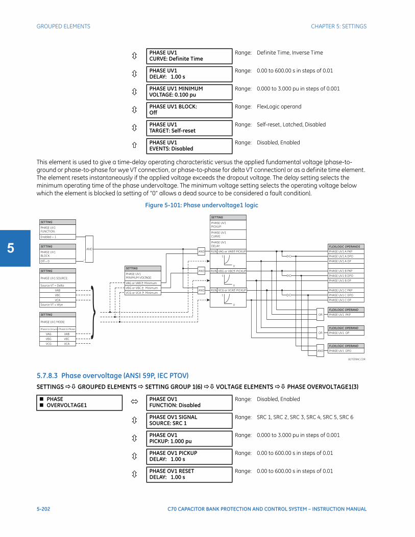
5-202 C70 CAPACITOR BANK PROTECTION AND CONTROL SYSTEM – INSTRUCTION MANUAL
GROUPED ELEMENTS CHAPTER 5: SETTINGS
5
This element is used to give a time-delay operating characteristic versus the applied fundamental voltage (phase-to-ground or phase-to-phase for wye VT connection, or phase-to-phase for delta VT connection) or as a definite time element. The element resets instantaneously if the applied voltage exceeds the dropout voltage. The delay setting selects the minimum operating time of the phase undervoltage. The minimum voltage setting selects the operating voltage below which the element is blocked (a setting of “0” allows a dead source to be considered a fault condition).
Figure 5-101: Phase undervoltage1 logic
5.7.8.3 Phase overvoltage (ANSI 59P, IEC PTOV)SETTINGS GROUPED ELEMENTS SETTING GROUP 1(6) VOLTAGE ELEMENTS PHASE OVERVOLTAGE1(3)
PHASE UV1CURVE: Definite Time
Range: Definite Time, Inverse Time
PHASE UV1DELAY: 1.00 s
Range: 0.00 to 600.00 s in steps of 0.01
PHASE UV1 MINIMUMVOLTAGE: 0.100 pu
Range: 0.000 to 3.000 pu in steps of 0.001
PHASE UV1 BLOCK:Off
Range: FlexLogic operand
PHASE UV1TARGET: Self-reset
Range: Self-reset, Latched, Disabled
PHASE UV1EVENTS: Disabled
Range: Disabled, Enabled
PHASE OVERVOLTAGE1 PHASE OV1
FUNCTION: DisabledRange: Disabled, Enabled
PHASE OV1 SIGNALSOURCE: SRC 1
Range: SRC 1, SRC 2, SRC 3, SRC 4, SRC 5, SRC 6
PHASE OV1PICKUP: 1.000 pu
Range: 0.000 to 3.000 pu in steps of 0.001
PHASE OV1 PICKUPDELAY: 1.00 s
Range: 0.00 to 600.00 s in steps of 0.01
PHASE OV1 RESETDELAY: 1.00 s
Range: 0.00 to 600.00 s in steps of 0.01

CHAPTER 5: SETTINGS GROUPED ELEMENTS
C70 CAPACITOR BANK PROTECTION AND CONTROL SYSTEM – INSTRUCTION MANUAL 5-203
5
There are three phase overvoltage elements available. A phase overvoltage element is used as an instantaneous element with no intentional time delay or as a definite time element. The input voltage is the phase-to-phase voltage, either measured directly from delta-connected VTs or as calculated from phase-to-ground (wye) connected VTs. The figure shows specific voltages to be used for each phase.
Figure 5-102: Phase overvoltage logic
5.7.8.4 Neutral overvoltage (ANSI 59N, IEC PTOV)SETTINGS GROUPED ELEMENTS SETTING GROUP 1(6) VOLTAGE ELEMENTS NEUTRAL OV1(3)
PHASE OV1 BLOCK:Off
Range: FlexLogic Operand
PHASE OV1TARGET: Self-reset
Range: Self-reset, Latched, Disabled
PHASE OV1EVENTS: Disabled
Range: Disabled, Enabled
NOTE
If the source VT is wye-connected, then the phase overvoltage pickup condition is for VAB, VBC, and VCA.
NEUTRAL OV1 NEUTRAL OV1
FUNCTION: DisabledRange: Disabled, Enabled
NEUTRAL OV1 SIGNALSOURCE: SRC 1
Range: SRC 1, SRC 2, SRC 3, SRC 4, SRC 5, SRC 6
NEUTRAL OV1 PICKUP:0.300 pu
Range: 0.000 to 3.000 pu in steps of 0.001
NEUTRAL OV1 CURVE:Definite time
Range: Definite time, FlexCurve A, FlexCurve B,FlexCurve C
NEUTRAL OV1 PICKUP:DELAY: 1.00 s
Range: 0.00 to 600.00 s in steps of 0.01
NEUTRAL OV1 RESET:DELAY: 1.00 s
Range: 0.00 to 600.00 s in steps of 0.01
NEUTRAL OV1 BLOCK:Off
Range: FlexLogic operand
PHASE OV1
SOURCE:
Source VT = Delta
Source VT = Wye
VAB
VBC
VCA
PHASE OV1 A PKP
PHASE OV1 B PKP
PHASE OV1 C PKP
PHASE OV1 OP
PHASE OV1 A DPO
PHASE OV1 B DPO
PHASE OV1 C DPO
PHASE OV1 A OP
PHASE OV1 B OP
PHASE OV1 C OP
PHASE OV1 DPO
AND
PHASE OV1
FUNCTION:
Disabled = 0
Enabled = 1
SETTING
PHASE OV1
BLOCK:
Off = 0
SETTING
SETTING
PHASE OV1
PICKUP:
SETTING
FLEXLOGIC OPERANDS
FLEXLOGIC OPERAND
FLEXLOGIC OPERAND
827066A7.CDR
RUN
VAB PICKUP≥
RUN
VBC PICKUP≥
RUN
VCA PICKUP≥
AND
OR
PHASE OV1 PKP
FLEXLOGIC OPERAND
OR
PHASE OV1 RESET
DELAY:
SETTINGS
tPKP
tPKP
tPKP
tRST
tRST
tRST
PHASE OV1 PICKUP
DELAY:
V 3 Pickup×>
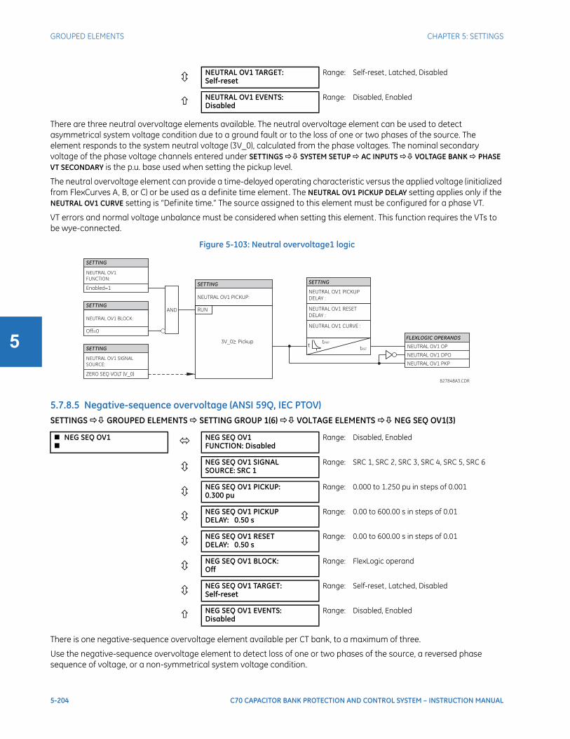
5-204 C70 CAPACITOR BANK PROTECTION AND CONTROL SYSTEM – INSTRUCTION MANUAL
GROUPED ELEMENTS CHAPTER 5: SETTINGS
5
There are three neutral overvoltage elements available. The neutral overvoltage element can be used to detect asymmetrical system voltage condition due to a ground fault or to the loss of one or two phases of the source. The element responds to the system neutral voltage (3V_0), calculated from the phase voltages. The nominal secondary voltage of the phase voltage channels entered under SETTINGS SYSTEM SETUP AC INPUTS VOLTAGE BANK PHASE VT SECONDARY is the p.u. base used when setting the pickup level.
The neutral overvoltage element can provide a time-delayed operating characteristic versus the applied voltage (initialized from FlexCurves A, B, or C) or be used as a definite time element. The NEUTRAL OV1 PICKUP DELAY setting applies only if the NEUTRAL OV1 CURVE setting is “Definite time.” The source assigned to this element must be configured for a phase VT.
VT errors and normal voltage unbalance must be considered when setting this element. This function requires the VTs to be wye-connected.
Figure 5-103: Neutral overvoltage1 logic
5.7.8.5 Negative-sequence overvoltage (ANSI 59Q, IEC PTOV)SETTINGS GROUPED ELEMENTS SETTING GROUP 1(6) VOLTAGE ELEMENTS NEG SEQ OV1(3)
There is one negative-sequence overvoltage element available per CT bank, to a maximum of three.
Use the negative-sequence overvoltage element to detect loss of one or two phases of the source, a reversed phase sequence of voltage, or a non-symmetrical system voltage condition.
NEUTRAL OV1 TARGET:Self-reset
Range: Self-reset, Latched, Disabled
NEUTRAL OV1 EVENTS:Disabled
Range: Disabled, Enabled
NEG SEQ OV1 NEG SEQ OV1
FUNCTION: DisabledRange: Disabled, Enabled
NEG SEQ OV1 SIGNALSOURCE: SRC 1
Range: SRC 1, SRC 2, SRC 3, SRC 4, SRC 5, SRC 6
NEG SEQ OV1 PICKUP:0.300 pu
Range: 0.000 to 1.250 pu in steps of 0.001
NEG SEQ OV1 PICKUPDELAY: 0.50 s
Range: 0.00 to 600.00 s in steps of 0.01
NEG SEQ OV1 RESETDELAY: 0.50 s
Range: 0.00 to 600.00 s in steps of 0.01
NEG SEQ OV1 BLOCK:Off
Range: FlexLogic operand
NEG SEQ OV1 TARGET:Self-reset
Range: Self-reset, Latched, Disabled
NEG SEQ OV1 EVENTS:Disabled
Range: Disabled, Enabled

CHAPTER 5: SETTINGS GROUPED ELEMENTS
C70 CAPACITOR BANK PROTECTION AND CONTROL SYSTEM – INSTRUCTION MANUAL 5-205
5
Figure 5-104: Negative-sequence overvoltage logic
5.7.8.6 Auxiliary overvoltage (ANSI 59X, IEC PTOV)SETTINGS GROUPED ELEMENTS SETTING GROUP 1(6) VOLTAGE ELEMENTS AUXILIARY OV1(3)
The C70 contains one auxiliary overvoltage element for each VT bank. This element is intended for monitoring overvoltage conditions of the auxiliary voltage. The nominal secondary voltage of the auxiliary voltage channel entered under SYSTEM SETUP AC INPUTS VOLTAGE BANK X5 AUXILIARY VT X5 SECONDARY is the per-unit (pu) base used when setting the pickup level.
AUXILIARY OV1 AUX OV1
FUNCTION: DisabledRange: Disabled, Enabled
AUX OV1 SIGNALSOURCE: SRC 1
Range: SRC 1, SRC 2, SRC 3, SRC 4, SRC 5, SRC 6
AUX OV1 PICKUP:0.300 pu
Range: 0.000 to 3.000 pu in steps of 0.001
AUX OV1 PICKUPDELAY: 1.00 s
Range: 0.00 to 600.00 s in steps of 0.01
AUX OV1 RESETDELAY: 1.00 s
Range: 0.00 to 600.00 s in steps of 0.01
AUX OV1 BLOCK:Off
Range: FlexLogic operand
AUX OV1 TARGET:Self-reset
Range: Self-reset, Latched, Disabled
AUX OV1 EVENTS:Disabled
Range: Disabled, Enabled

5-206 C70 CAPACITOR BANK PROTECTION AND CONTROL SYSTEM – INSTRUCTION MANUAL
GROUPED ELEMENTS CHAPTER 5: SETTINGS
5
Figure 5-105: Auxiliary overvoltage logic
5.7.8.7 Bank voltage differential (ANSI 87V, IEC PDIF)SETTINGS GROUPED ELEMENTS SETTING GROUP 1(6) VOLTAGE ELEMENTS VOLTAGE DIFFERENTIAL 1(3)
VOLTAGE DIFFERENTIAL 1 VOLTAGE DIF 1
FUNCTION: DisabledRange: Disabled, Enabled
VOLTAGE DIF 1 BUSSOURCE: SRC 1
Range: SRC 1, SRC 2, SRC 3, SRC 4, SRC 5, SRC 6
VOLTAGE DIF 1 TAPSOURCE: SRC 1
Range: SRC 1, SRC 2, SRC 3, SRC 4, SRC 5, SRC 6
VOLTAGE DIF 1 BANKGROUND: Grounded
Range: Grounded, Ungrounded
VOLTAGE DIF 1 MATCHFACTOR A: 2.0000
Range: 0.5000 to 2000.0000 in steps of 0.0001
VOLTAGE DIF 1 MATCHFACTOR B: 2.0000
Range: 0.5000 to 2000.0000 in steps of 0.0001
VOLTAGE DIF 1 MATCHFACTOR C: 2.0000
Range: 0.5000 to 2000.0000 in steps of 0.0001
VOLTAGE DIF 1 STG 1APICKUP: 0.010 pu
Range: 0.001 to 1.000 pu in steps of 0.001
VOLTAGE DIF 1 STG 2APICKUP: 0.020 pu
Range: 0.001 to 1.000 pu in steps of 0.001
VOLTAGE DIF 1 STG 3APICKUP: 0.030 pu
Range: 0.001 to 1.000 pu in steps of 0.001
VOLTAGE DIF 1 STG 4APICKUP: 0.040 pu
Range: 0.001 to 1.000 pu in steps of 0.001
VOLTAGE DIF 1 STG 1BPICKUP: 0.010 pu
Range: 0.001 to 1.000 pu in steps of 0.001
VOLTAGE DIF 1 STG 2BPICKUP: 0.020 pu
Range: 0.001 to 1.000 pu in steps of 0.001
VOLTAGE DIF 1 STG 3BPICKUP: 0.030 pu
Range: 0.001 to 1.000 pu in steps of 0.001
VOLTAGE DIF 1 STG 4BPICKUP: 0.040 pu
Range: 0.001 to 1.000 pu in steps of 0.001
VOLTAGE DIF 1 STG 1CPICKUP: 0.010 pu
Range: 0.001 to 1.000 pu in steps of 0.001

CHAPTER 5: SETTINGS GROUPED ELEMENTS
C70 CAPACITOR BANK PROTECTION AND CONTROL SYSTEM – INSTRUCTION MANUAL 5-207
5
Up to three identical voltage differential elements, one per each VT bank configured in hardware, are provided.
The element responds to a differential signal between magnitudes of the bus and tap voltages. The latter is scaled using a matching factor to account for the position of the tap. An automatic setting procedure is available under the COMMAND menu to calculate automatically the matching factor when installing the relay or after repairs of the bank.
VOLTAGE DIF 1 STG 2CPICKUP: 0.020 pu
Range: 0.001 to 1.000 pu in steps of 0.001
VOLTAGE DIF 1 STG 3CPICKUP: 0.030 pu
Range: 0.001 to 1.000 pu in steps of 0.001
VOLTAGE DIF 1 STG 4CPICKUP: 0.040 pu
Range: 0.001 to 1.000 pu in steps of 0.001
VOLTAGE DIF 1 STG 1PKP DELAY: 30.00 s
Range: 0.00 to 600.00 s in steps of 0.01
VOLTAGE DIF 1 STG 2PKP DELAY: 10.00 s
Range: 0.00 to 600.00 s in steps of 0.01
VOLTAGE DIF 1 STG 3PKP DELAY: 1.00 s
Range: 0.00 to 600.00 s in steps of 0.01
VOLTAGE DIF 1 STG 4PKP DELAY: 0.20 s
Range: 0.00 to 600.00 s in steps of 0.01
VOLTAGE DIF 1DPO DELAY: 0.25 s
Range: 0.00 to 600.00 s in steps of 0.01
VOLT DIF 1 BLK STG1:Off
Range: FlexLogic operand
VOLT DIF 1 BLK STG 2:Off
Range: FlexLogic operand
VOLT DIF 1 BLK STG 3:Off
Range: FlexLogic operand
VOLT DIF 1 BLK STG 4:Off
Range: FlexLogic operand
VOLT DIF 1 TARGET:Self-Reset
Range: Self-reset, Latched, Disabled
VOLT DIF 1 EVENTS:Disabled
Range: Disabled, Enabled
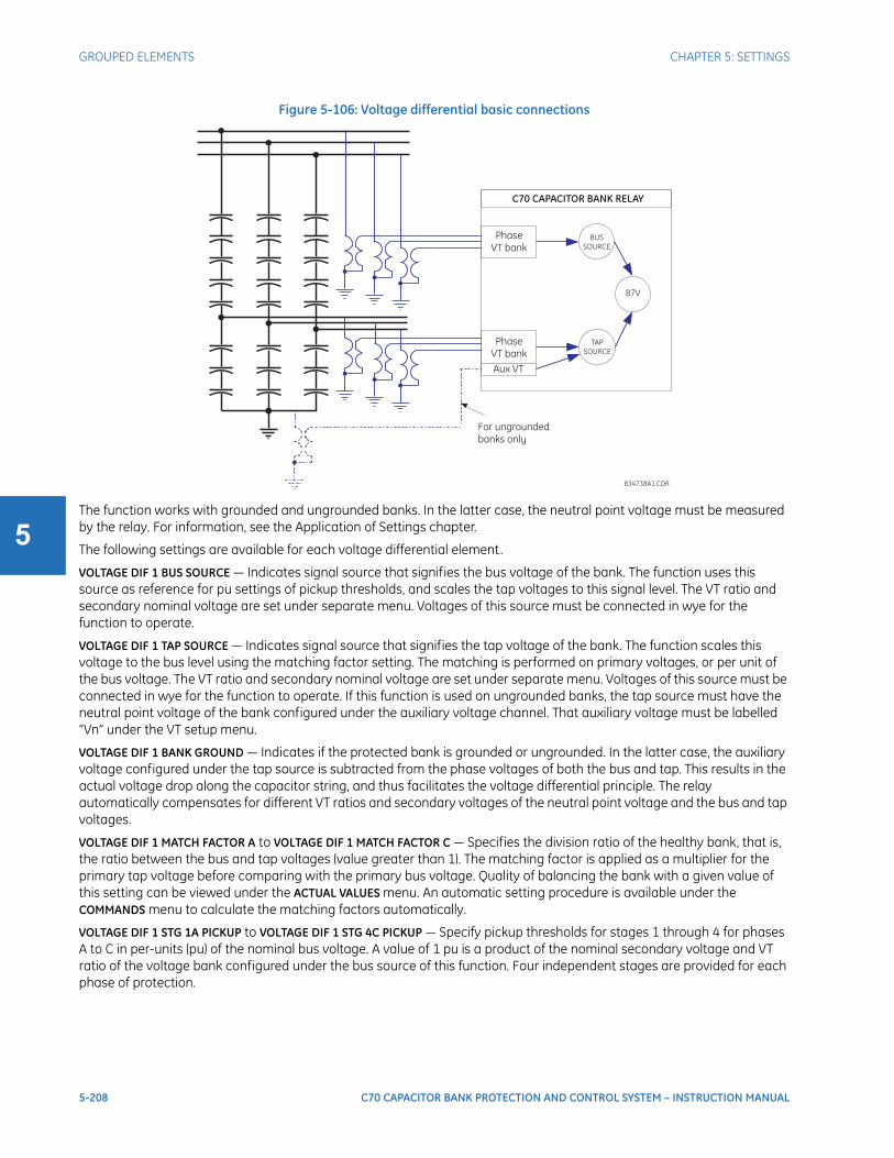
5-208 C70 CAPACITOR BANK PROTECTION AND CONTROL SYSTEM – INSTRUCTION MANUAL
GROUPED ELEMENTS CHAPTER 5: SETTINGS
5
Figure 5-106: Voltage differential basic connections
The function works with grounded and ungrounded banks. In the latter case, the neutral point voltage must be measured by the relay. For information, see the Application of Settings chapter.
The following settings are available for each voltage differential element.
VOLTAGE DIF 1 BUS SOURCE — Indicates signal source that signifies the bus voltage of the bank. The function uses this source as reference for pu settings of pickup thresholds, and scales the tap voltages to this signal level. The VT ratio and secondary nominal voltage are set under separate menu. Voltages of this source must be connected in wye for the function to operate.
VOLTAGE DIF 1 TAP SOURCE — Indicates signal source that signifies the tap voltage of the bank. The function scales this voltage to the bus level using the matching factor setting. The matching is performed on primary voltages, or per unit of the bus voltage. The VT ratio and secondary nominal voltage are set under separate menu. Voltages of this source must be connected in wye for the function to operate. If this function is used on ungrounded banks, the tap source must have the neutral point voltage of the bank configured under the auxiliary voltage channel. That auxiliary voltage must be labelled “Vn” under the VT setup menu.
VOLTAGE DIF 1 BANK GROUND — Indicates if the protected bank is grounded or ungrounded. In the latter case, the auxiliary voltage configured under the tap source is subtracted from the phase voltages of both the bus and tap. This results in the actual voltage drop along the capacitor string, and thus facilitates the voltage differential principle. The relay automatically compensates for different VT ratios and secondary voltages of the neutral point voltage and the bus and tap voltages.
VOLTAGE DIF 1 MATCH FACTOR A to VOLTAGE DIF 1 MATCH FACTOR C — Specifies the division ratio of the healthy bank, that is, the ratio between the bus and tap voltages (value greater than 1). The matching factor is applied as a multiplier for the primary tap voltage before comparing with the primary bus voltage. Quality of balancing the bank with a given value of this setting can be viewed under the ACTUAL VALUES menu. An automatic setting procedure is available under the COMMANDS menu to calculate the matching factors automatically.
VOLTAGE DIF 1 STG 1A PICKUP to VOLTAGE DIF 1 STG 4C PICKUP — Specify pickup thresholds for stages 1 through 4 for phases A to C in per-units (pu) of the nominal bus voltage. A value of 1 pu is a product of the nominal secondary voltage and VT ratio of the voltage bank configured under the bus source of this function. Four independent stages are provided for each phase of protection.
C70 CAPACITOR BANK RELAY
87V
BUS
SOURCE
TAP
SOURCE
Phase
VT bank
Aux VT
For ungrounded
banks only
Phase
VT bank
834738A1.CDR

CHAPTER 5: SETTINGS GROUPED ELEMENTS
C70 CAPACITOR BANK PROTECTION AND CONTROL SYSTEM – INSTRUCTION MANUAL 5-209
5
VOLTAGE DIF 1 STG 1 PKP DELAY — Specifies the pickup time delay, individually per each stage of alarming/tripping. Note that each of the 12 comparators (four stages in three phases) uses an individual timer, but settings for these timers are controlled individually per each stage, not per phase. The timers use a common drop-out time delay specified by the next setting.
VOLTAGE DIF 1 DPO DELAY — Controls a drop out delay for the operate FlexLogic operands. Note that individual stages apply individually configurable pickup delays, but use this common drop out delay.
VOLT DIF 1 BLK STG 1 to VOLT DIF 1 BLK STG 4 — These inputs are used to block the function on a per stage basis when required. At minimum this function shall be blocked when the bank is offline, or else it operates unnecessarily. Either breaker position or undercurrent indication via any available instantaneous function, or a combination, can be used for blocking. Also consider the VT fuse fail condition from both the bus and tap VT. When unblocked, the function becomes operational after five cycles of intentional delay.
Figure 5-107: Voltage differential logic
5.7.8.8 Bank phase overvoltage (ANSI 59B, IEC PTOV)SETTINGS GROUPED ELEMENTS SETTING GROUP 1(6) VOLTAGE ELEMENTS BANK OVERVOLTAGE BANK OVERVOLTAGE 1(3)
BANK OVERVOLTAGE 1 BANK OV 1
FUNCTION: DisabledRange: Disabled, Enabled
BANK OV 1 BUSSOURCE: SRC 1
Range: SRC 1, SRC 2, SRC 3, SRC 4, SRC 5, SRC 6
tPKP
t DPO
tPKP
tDPO
tPKP
tDPO
SETTINGS
VOLTAGE DIF 1 BUS
SOURCE:
V1A
V1B
V1C
VOLTAGE DIF 1 TAP
SOURCE:
V2A
V2B
V2C
VN
SETTINGS
VA
_d
if=
|V
A_
ma
g-
kA
*V
2A
_m
ag
|
or
|V
A_
ma
g-
kA
*(V
2A
-V
N)_
ma
g|
VOLTAGE DIF 1
MATCH FACTOR A:
SETTING
VOLTAGE DIF 1 STG
1A PICKUP:
SETTING
VOLTAGE DIF 1 STG
2A PICKUP:
SETTING
VOLTAGE DIF 1 STG
3A PICKUP:
SETTING
VOLTAGE DIF 1 STG
4A PICKUP:
VOLT DIF 1 STG 1A PKP
FLEXLOGIC OPERAND
VOLT DIF 1 STG 2A PKP
FLEXLOGIC OPERAND
VOLT DIF 1 STG 3A PKP
FLEXLOGIC OPERAND
VOLT DIF 1 STG 4A PKP
FLEXLOGIC OPERAND
tPKP
tDPO
TIMERS
VOLTAGE DIF 1 STG 1
PKP DELAY:
VOLTAGE DIF 1 STG 2
PKP DELAY:
VOLTAGE DIF 1 STG 3
PKP DELAY:
VOLTAGE DIF 1 STG 4
PKP DELAY:
VOLT DIF 1 STG 1A OP
VOLT DIF 1 STG 2A OP
VOLT DIF 1 STG 3A OP
FLEXLOGIC OPERAND
VOLT DIF 1 STG 4A OP
VOLT DIF 1 PKP B
VOLTAGE DIF 1 DPO
DELAY:
VOLT DIF 1 PKP A
VOLT DIF 1 PKP C
OR
VOLT DIF 1 PKPOR
VOLT DIF 1 OP B
VOLT DIF 1 OP A
VOLT DIF 1 OP C
OR
VOLT DIF 1 OPOR
VOLT DIF 1 DPO
PHASE C
5 cycles
0
TIMER
RUN 87V FUNCTION
PHASE B
COMMANDS
AUTO-SETTING
PROCEDURE
VOLTAGE DIF 1 BANK
GROUND:
SETTING
COMMANDS/
VOLTAGE DIF 1
AUTO-SETTING:
WRITE A NEW SETTING
AN
D
VC_mag > 0.25 pu
VB_mag > 0.25 pu
VA_mag > 0.25 pu
SETTINGS
VOLTAGE DIF 1
FUNCTION:
Enabled = 1
VOLT DIF 1 BLK STG1:
Off = 0
VOLT DIF 1 BLK STG2:
Off = 0
VOLT DIF 1 BLK STG3:
Off = 0
VOLT DIF 1 BLK STG4:
Off = 0
AN
D
INHIBIT STAGE 1
INHIBIT STAGE 3
INHIBIT STAGE 4
INHIBIT STAGE 2
AN
D
Manual
Auto AN
D
Apply?
FLEXLOGIC OPERAND
FLEXLOGIC OPERAND
FLEXLOGIC OPERAND
FLEXLOGIC OPERAND
FLEXLOGIC OPERANDFLEXLOGIC OPERAND
FLEXLOGIC OPERAND
VA_dif > PICKUP
RUNAN
D
VA_dif > PICKUP
RUNAN
D
VA_dif > PICKUP
RUNAN
D
VA_dif > PICKUP
RUNAN
D
834742A1.DWG
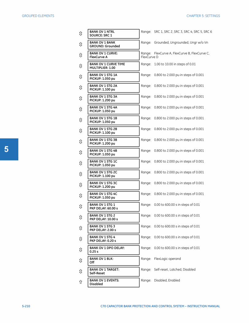
5-210 C70 CAPACITOR BANK PROTECTION AND CONTROL SYSTEM – INSTRUCTION MANUAL
GROUPED ELEMENTS CHAPTER 5: SETTINGS
5
BANK OV 1 NTRLSOURCE: SRC 1
Range: SRC 1, SRC 2, SRC 3, SRC 4, SRC 5, SRC 6
BANK OV 1 BANKGROUND: Grounded
Range: Grounded, Ungrounded, Ungr w/o Vn
BANK OV 1 CURVE:FlexCurve A
Range: FlexCurve A, FlexCurve B, FlexCurve C,FlexCurve D
BANK OV 1 CURVE TIMEMULTIPLIER: 1.00
Range: 1.00 to 10.00 in steps of 0.01
BANK OV 1 STG 1APICKUP: 1.050 pu
Range: 0.800 to 2.000 pu in steps of 0.001
BANK OV 1 STG 2APICKUP: 1.100 pu
Range: 0.800 to 2.000 pu in steps of 0.001
BANK OV 1 STG 3APICKUP: 1.200 pu
Range: 0.800 to 2.000 pu in steps of 0.001
BANK OV 1 STG 4APICKUP: 1.050 pu
Range: 0.800 to 2.000 pu in steps of 0.001
BANK OV 1 STG 1BPICKUP: 1.050 pu
Range: 0.800 to 2.000 pu in steps of 0.001
BANK OV 1 STG 2BPICKUP: 1.100 pu
Range: 0.800 to 2.000 pu in steps of 0.001
BANK OV 1 STG 3BPICKUP: 1.200 pu
Range: 0.800 to 2.000 pu in steps of 0.001
BANK OV 1 STG 4BPICKUP: 1.050 pu
Range: 0.800 to 2.000 pu in steps of 0.001
BANK OV 1 STG 1CPICKUP: 1.050 pu
Range: 0.800 to 2.000 pu in steps of 0.001
BANK OV 1 STG 2CPICKUP: 1.100 pu
Range: 0.800 to 2.000 pu in steps of 0.001
BANK OV 1 STG 3CPICKUP: 1.200 pu
Range: 0.800 to 2.000 pu in steps of 0.001
BANK OV 1 STG 4CPICKUP: 1.050 pu
Range: 0.800 to 2.000 pu in steps of 0.001
BANK OV 1 STG 1PKP DELAY: 60.00 s
Range: 0.00 to 600.00 s in steps of 0.01
BANK OV 1 STG 2PKP DELAY: 10.00 s
Range: 0.00 to 600.00 s in steps of 0.01
BANK OV 1 STG 3PKP DELAY: 2.00 s
Range: 0.00 to 600.00 s in steps of 0.01
BANK OV 1 STG 4PKP DELAY: 0.20 s
Range: 0.00 to 600.00 s in steps of 0.01
BANK OV 1 DPO DELAY:0.25 s
Range: 0.00 to 600.00 s in steps of 0.01
BANK OV 1 BLK:Off
Range: FlexLogic operand
BANK OV 1 TARGET:Self-Reset
Range: Self-reset, Latched, Disabled
BANK OV 1 EVENTS:Disabled
Range: Disabled, Enabled

CHAPTER 5: SETTINGS GROUPED ELEMENTS
C70 CAPACITOR BANK PROTECTION AND CONTROL SYSTEM – INSTRUCTION MANUAL 5-211
5
Up to three identical bank overvoltage elements, one per each VT bank configured in hardware, are provided.
The bank phase overvoltage element responds to voltages across the capacitors of the bank. Three stages of definite time operation, and one stage of inverse time operation are provided. Pickup thresholds of this function are adjustable on a per-phase basis. The shape of the inverse time curve is user-programmable (via FlexCurves™) with individual pickup levels and a multiplier common for all three phases. The definite time delays are individually programmable per stage.
The function works with grounded and ungrounded banks. With ungrounded banks, either the neutral point voltage is measured by the relay and used to derive the true bank voltage based on the bus and neutral-point voltages, or a simplified method to provide proper voltage protection is used responding to vector differences between the phase-to-phase voltages.
When fed from wye-connected VTs, the function responds to phase-to-ground voltages. When fed from delta-connected VTs, it responds to the vector difference between the phase-to-phase voltages.
The function responds to true RMS voltages to account for effects of harmonics (harmonics impacting losses in the capacitor, harmonics increasing peak values in the voltages compared with the filtered fundamental frequency magnitudes).
Figure 5-108: Bank overvoltage basic connections
For more information, see the Application of Settings chapter.
The following settings are available for each bank phase overvoltage element.
BANK OV 1 BUS SOURCE — Indicates the signal source that signifies the bus voltage of the capacitor bank. The function uses this source as reference for per-unit (pu) settings of the pickup thresholds. The VT ratio and secondary nominal voltage are set under the SETTINGS SYSTEM SETUP AC INPUTS VOLTAGE BANK menu.
BANK OV 1 NTRL SOURCE — Indicates the signal source that signifies the neutral-point voltage of the bank. The auxiliary voltage channel of this source is used, and must be labelled “Vn” under the VT setup menu. The neutral point voltage is used only when the function is applied to an ungrounded bank, to derive the true voltage drop across the capacitors. The VT ratio and secondary nominal voltage are set under the SETTINGS SYSTEM SETUP AC INPUTS VOLTAGE BANK menu.
Alternative: delta
connected VTs
C70 CAPACITOR BANK RELAY
59B
BUS
SRC
NTRL
SRC
Phase
VT Bank
Aux VT
For ungrounded
banks only
834734A1.DWG
5-212 C70 CAPACITOR BANK PROTECTION AND CONTROL SYSTEM – INSTRUCTION MANUAL
GROUPED ELEMENTS CHAPTER 5: SETTINGS
5
BANK OV 1 BANK GROUND — This setting indicates if the protected bank is grounded, ungrounded with the neutral point voltage measured, and ungrounded without the neutral point voltage. The relay automatically compensates for potentially different VT ratios and secondary voltages of the bus and neutral point voltages. The following table explains the operating signals of the function based on the input signals available to the relay.
Table 5-34: Operating signals based on input signals
BANK OV 1 CURVE — This setting specifies a FlexCurve used by the fourth inverse time stage of this function. FlexCurves are user-programmable on a point-by-point basis. This function applies a common curve shape in all three phases. However, the curve is specified as time versus multiple of pickup. With three individually programmable pickup values per phase one accommodates possible differences between individual phases of the bank even though a common curve shape is used.
Implementation of the inverse-time stage is based on the concept of a virtual disk emulating electromechanical relays. When above the pickup level, the function integrates towards the trip level at the rate dictated by the curve at a given multiple of pickup. When activated but with the operating signal below the pickup, the function integrates down toward a complete reset. This mode of operation assures dependability in situations when the voltage oscillates and causes stress to the protected capacitor in repetitive cycles each lasting too short to expire a straight timer. As a result of this implementation, the shape of the curve below multiple of pickup of 1 is important as it controls the speed of reset of a partially energized function.
BANK OV 1 STG 1A PICKUP to BANK OV 1 STG 3C PICKUP — Specify pickup thresholds for stages 1 through 3 in phases A through C in per-units (pu) of the nominal phase-to-ground bus voltage. A value of 1 pu is a product of the nominal secondary voltage and VT ratio of the voltage bank configured under the bus source of this function. With a delta VT configuration, a value of 1 pu is a product of the nominal secondary voltage and VT ratio divided by . Three independent stages of definite-time operation are provided for each phase of the bank.
BANK OV 1 STG 4A PICKUP to BANK OV 1 STG 4C PICKUP — Secify pickup thresholds for the inverse time stage 4 in phase A through C in per-units (pu) of the nominal phase-to-ground bus voltage. With a wye VT configuration, a value of 1 pu is a product of the nominal secondary voltage and VT ratio of the voltage bank configured under the bus source of this function. With a delta VT configuration, a value of 1 pu is a product of the nominal secondary voltage and VT ratio divided by . The inverse time stage uses a user-programmable FlexCurve selected by the BANK OV 1 CURVE setting.
BANK OV 1 STG 1 PKP DELAY to BANK OV 1 STG 3 PKP DELAY — Specify the pickup time delays for each definite time stage of alarming/tripping. Note that each of the nine comparators (three definite-time stages in three phases) uses an individual timer, but settings for these timers are controlled individually per each stage, not per phase. The timers use a common dropout time delay specified by the BANK OV 1 DPO DELAY setting.
BANK OV 1 DPO DELAY — This setting controls a dropout delay for the operate FlexLogic operands. Note that individual stages apply individually configurable pickup delays, but use this common dropout delay.
BANK OV 1 BLK — This input is used to block the function when required; in particular, when the bank is offline.
VT connection Bank configuration
Grounded Ungrounded Ungrounded w/o VN
Wye Vop_A = VAVop_B = VBVop_C = VC
Vop_A = VA – VXVop_B = VB – VXVop_C = VC – VX
Vop_A = (VCA – VAB) / 3Vop_B = (VAB – VBC) / 3Vop_C = (VBC – VCA) / 3
Delta Vop_A = (VCA – VAB) / 3Vop_B = (VAB – VBC) / 3Vop_C = (VBC – VCA) / 3
3
3

CHAPTER 5: SETTINGS GROUPED ELEMENTS
C70 CAPACITOR BANK PROTECTION AND CONTROL SYSTEM – INSTRUCTION MANUAL 5-213
5
Figure 5-109: Bank phase overvoltage logic
5.7.8.9 Neutral voltage unbalance (ANSI 59NU, IEC PVCB/PTOV)SETTINGS GROUPED ELEMENTS SETTING GROUP 1(6) VOLTAGE ELEMENTS NEUTRAL VOLTAGE UNBALANCE 1(3)
NEUTRAL VOLTAGE UNBALANCE 1 NTRL VOL UNBAL 1
FUNCTION: DisabledRange: Disabled, Enabled
NTRL VOL UNBAL 1NTRL SOURCE: SRC 1
Range: SRC 1, SRC 2, SRC 3, SRC 4, SRC 5, SRC 6
NTRL VOL UNBAL 1BUS SOURCE: SRC 1
Range: SRC 1, SRC 2, SRC 3, SRC 4, SRC 5, SRC 6
NTRL VOL UNBAL 1 BUS3V0: Calculated
Range: Calculated, Measured
NTRL VOL UNBAL 1GROUND: VT (ungrnd)
Range: VT (ungrnd), CTxR (grnd)
NTRL VOL UNBAL 1AB RATIO: 1.0000
Range: 0.7500 to 1.2500 in steps of 0.0001
NTRL VOL UNBAL 1AC RATIO: 1.0000
Range: 0.7500 to 1.2500 in steps of 0.0001
NTRL VOL UNBAL 1STG 1 PKP: 0.010 pu
Range: 0.001 to 1.000 pu in steps of 0.001
NTRL VOL UNBAL 1STG 1 SLOPE: 0.0%
Range: 0.0 to 10.0% in steps of 0.1
NTRL VOL UNBAL 1STG 2 PKP: 0.020 pu
Range: 0.001 to 1.000 pu in steps of 0.001
tPKP
tDPO
tPKP
tDPO
SETTINGS
BANK OV 1 BUS
SOURCE:
Va
Vb
Vc
BANK OV 1 NTRL
SOURCE:
Vx
AN
D
SETTING
VA_op = Va RMS
OR
VA_op = (va - vx) RMS
or
VA_op = (vca - vab)/3
RMS
VA_op> PICKUP
SETTING
BANK OV 1 STG 1A
PICKUP:
SETTING
BANK OV 1 STG 2A
PICKUP:
SETTING
BANK OV 1 STG 3A
PICKUP:
SETTING
BANK OV 1 STG 4A
PICKUP:
BANK OV 1 STG 1A PKP
FLEXLOGIC OPERAND
BANK OV 1 STG 2A PKP
FLEXLOGIC OPERAND
BANK OV 1 STG 3A PKP
FLEXLOGIC OPERAND
BANK OV 1 STG 4A PKP
FLEXLOGIC OPERAND
tPKP
tDPO
TIMERS
BANK OV 1 STG 1 PKP
DELAY:
BANK OV 1 STG 2 PKP
DELAY:
BANK OV 1 STG 3 PKP
DELAY:
BANK OV 1 STG 1A OP
FLEXLOGIC OPERAND
BANK OV 1 STG 2A OP
FLEXLOGIC OPERAND
BANK OV 1 STG 3A OP
FLEXLOGIC OPERAND
BANK OV 1 STG 4A OP
FLEXLOGIC OPERAND
BANK OV 1 PKP B
FLEXLOGIC OPERANDS
BANK OV 1 DPO
DELAY:
BANK OV 1 PKP A
BANK OV 1 PKP C
OR
FLEXLOGIC OPERAND
BANK OV 1 PKPOR
BANK OV 1 OP B
FLEXLOGIC OPERANDS
BANK OV 1 OP A
BANK OV 1 OP C
OR
FLEXLOGIC OPERAND
BANK OV 1 OPOR
BANK OV 1 DPO
PHASE C
SETTINGS
BANK OV 1
FUNCTION:
Enabled = 1
BANK OV 1 BLK:
Off = 0
RUN 59B FUNCTION
PHASE B
BANK OV 1 BANK
GROUND:
BANK OV 1 CURVE
PKP
RUN
VA_op> PICKUP
VA_op> PICKUP
VA_op> PICKUP
RUN
RUN
RUN
834743A1.DWG
0
tDPO

5-214 C70 CAPACITOR BANK PROTECTION AND CONTROL SYSTEM – INSTRUCTION MANUAL
GROUPED ELEMENTS CHAPTER 5: SETTINGS
5
Up to three identical neutral voltage unbalance elements, one per each VT bank configured in hardware, are provided.
The element responds to the voltage signal at the neutral point of the capacitor bank. The operating equations are properly compensated for both the system unbalance such as during close-in external faults, and the inherent bank unbalance. The bus zero-sequence voltage required for compensation of the system unbalance can be measured internally to the relay from phase voltages, or delivered as a 3V0 signal from an open-corner-delta VT via an auxiliary voltage channel of the relay.
Compensation for the inherent unbalance of the protected bank uses the B and C phase voltages, and thus this function requires wye connected phase VTs. The inherent unbalance is zeroed out using ratios of the reactances between the reference phase A, and the two other phases. An automatic setting procedure is available under the COMMAND menu to calculate the compensating factors automatically when installing the relay, or after repairs of the bank.
To enhance performance under large system unbalances when the neutral-point and system zero-sequence voltages can become significant, a concept of a restraint is introduced. The slope of the operating characteristic is user adjustable, and if required, it can be effectively removed yielding a straight compensated overvoltage function.
For information, see the Application of Settings chapter.
NTRL VOL UNBAL 1STG 2 SLOPE: 0.0%
Range: 0.0 to 10.0% in steps of 0.1
NTRL VOL UNBAL 1STG 3 PKP: 0.020 pu
Range: 0.001 to 1.000 pu in steps of 0.001
NTRL VOL UNBAL 1STG 3 SLOPE: 5.0%
Range: 0.0 to 10.0% in steps of 0.1
NTRL VOL UNBAL 1STG 4 PKP: 0.030 pu
Range: 0.001 to 1.000 pu in steps of 0.001
NTRL VOL UNBAL 1STG 4 SLOPE: 5.0%
Range: 0.0 to 10.0% in steps of 0.1
NTRL VOL UNBAL 1 STG1 PKP DELAY: 30.00 s
Range: 0.00 to 600.00 s in steps of 0.01
NTRL VOL UNBAL 1 STG2 PKP DELAY: 10.00 s
Range: 0.00 to 600.00 s in steps of 0.01
NTRL VOL UNBAL 1 STG3 PKP DELAY: 1.00 s
Range: 0.00 to 600.00 s in steps of 0.01
NTRL VOL UNBAL 1 STG4 PKP DELAY: 0.20 s
Range: 0.00 to 600.00 s in steps of 0.01
NTRL VOL UNBAL 1DPO DELAY: 0.25 s
Range: 0.00 to 600.00 s in steps of 0.01
NTRL VOL 1 BLK STG1:Off
Range: FlexLogic operand
NTRL VOL 1 BLK STG2:Off
Range: FlexLogic operand
NTRL VOL 1 BLK STG3:Off
Range: FlexLogic operand
NTRL VOL 1 BLK STG4:Off
Range: FlexLogic operand
NTRL VOL UNBAL 1TARGET: Self-Reset
Range: Self-reset, Latched, Disabled
NTRL VOL UNBAL 1EVENTS: Disabled
Range: Disabled, Enabled

CHAPTER 5: SETTINGS GROUPED ELEMENTS
C70 CAPACITOR BANK PROTECTION AND CONTROL SYSTEM – INSTRUCTION MANUAL 5-215
5
Figure 5-110: Neutral voltage unbalance basic connection
The following settings are available for all three neutral voltage unbalance elements.
NTRL VOL UNBAL 1 NTRL SOURCE — Indicates signal source that signifies the neutral-point voltage of the protected bank. This single-phase voltage is to be configured under the auxiliary VT channel. The VT ratio and secondary nominal voltage are set under separate menu. Nominal voltage of this auxiliary channel becomes a unit (1 pu) for the pickup settings of this function.
NTRL VOL UNBAL 1 BUS SOURCE — Indicates signal source that signifies the bus voltages of the bank. This source must have the phase voltages configured in order to facilitate compensation for the inherent unbalance of the bank. The zero-sequence voltage required for system unbalance compensation can be derived from the phase voltages, or delivered to the relay from an external source, typically a broken-delta VT (the selection is controlled by the next setting of this function). In the latter case, the 3V0 signal is expected and must be wired and configured under the auxiliary voltage channel of this source. This 3V0 voltage must be labelled as “Vn” under the VT configuration. The VT ratio and secondary nominal voltage are set under separate menu. Phase voltages of this source must be connected in wye for the function to operate. The function uses several voltages potentially produced by VTs of different ratios and nominal secondary values. The relay scales all the signals automatically for meaningful calculations.
NTRL VOL UNBAL 1 BUS 3V0 — Specifies the source of the bus zero-sequence voltage required for system unbalance compensation. If set to “Calculated”, the relay would derive the zero-sequence voltage as a vector sum of the three phase voltages and will run the function if voltage in all three phases is greater than 0.25 pu. If set to “Measured”, the relay expects the 3V0 signal (not a V0) to be wired to the relay under the auxiliary channel of the bus source, and labelled as “Vn”. In this case, the voltage check to run this function is not performed.
NTRL VOL UNBAL 1 GROUND — Selects the grounding arrangement of the bank. For ungrounded banks, set it to “VT (ungrnd)”. When the bank neutral is solidly grounded through the CT with a resistor in the CT secondary, set it as “CTxR (grnd)”.
5-216 C70 CAPACITOR BANK PROTECTION AND CONTROL SYSTEM – INSTRUCTION MANUAL
GROUPED ELEMENTS CHAPTER 5: SETTINGS
5
When the “CTxR (grnd)” value is selected, the measured bank neutral point voltage is shifted by 90° lagging to compensate for the angular difference between the bus neutral voltage and the voltage derived from the bank neutral point current. Choose the value of resistor R so the voltage measured by the auxiliary input of the relay matches bus V0 during system faults (for example, an SLG fault at the bus). This is accomplished by the following condition:
Eq. 5-20
where
V0BUS is the bus primary zero-sequence voltage during system fault
3I0NTRL is the primary current in the bank neutral during system fault
nBUS_VT is the bus VT ratio set in the source selected by the NTRL VOL UNBAL 1 BUS SOURCE setting
nNTRL_VT is a neutral point VT ratio set in the source selected by the NTRL VOL UNBAL 1 NTRL SOURCE setting. If R can be chosen precisely, then nNTRL_VT can be set same as nBUS_VT. If R cannot be chosen precisely, then nNTRL_VT is used to match zero-sequence voltage as per the equation above.
nNTRL_CT is the CT ratio in the bank neutral
NTRL VOL UNBAL 1 AB RATIO — This setting compensates for the bank inherent unbalance. Physically this value is a ratio of the reactance in phase A divided by the reactance in phase B. Auto-setting procedure is available under the Commands menu to calculate this value automatically. When tuning this setting manually, after bank repairs, this ratio shall be increased or decreased from the nominal value of 1.00 depending on whether the A or B phase got affected by failures or repairs and whether a given reactance increased or decreased as a result of the failure or repair. Use this setting only when the NTRL VOL UNBAL 1 BUS 3V0 setting is set as “Calculated.”
NTRL VOL UNBAL 1 AC RATIO — Compensates for the bank inherent unbalance. Physically this value is a ratio of the reactance in phase A divided by the reactance in phase C. Auto-setting procedure is available under the Commands menu to calculate this value automatically. When tuning this setting manually, after bank repairs, this ratio shall be increased or decreased from the nominal value of 1.00 depending on whether the A or C phase got affected by failures or repairs and whether a given reactance increased or decreased as a result of the failure or repair. Use this setting only when the NTRL VOL UNBAL 1 BUS 3V0 setting is set as “Calculated”.
NTRL VOL UNBAL 1 STG 1 PKP to NTRL VOL UNBAL 1 STG 1 PKP — Specify pickup thresholds for stages 1 through 4 of the function in per-units (pu) of the nominal value of the neutral-point VT (the auxiliary channel of the neutral source).
NTRL VOL UNBAL 1 STG 1 SLOPE to NTRL VOL UNBAL 1 STG 4 SLOPE — Specify the slopes of the operating characteristic. Neglecting compensation for the inherent bank unbalance, the operating signal is a vectorial difference between the neutral point voltage and the zero-sequence bus voltage. Therefore, the optimum restraining signal is a vectorial sum of the two signals. During external ground faults, the two voltages are approximately in phase generating a large restraining signal being twice the zero-sequence voltage at the bus. A slope of few percent is typically sufficient to provide good security under large system unbalances. If a given stage is used with a time delay longer than the expected external fault duration, the slope may be reduced or eliminated. In general, the slope can be understood as a adaptive threshold, and the user is provided with three ways to control sensitivity and security: pickup, time delay and slope. See the Application of Settings chapter for information.
NTRL VOL UNBAL 1 STG 1 PKP DELAY to NTRL VOL UNBAL 1 STG 4 PKP DELAY — Specify the pickup time delays for each stage of alarming or tripping. Each of the four comparators (four stages) uses an individual pickup timer, but a common drop out time delay as specified by the next setting.
NTRL VOL UNBAL 1 DPO DELAY — Controls a drop out delay for the operate FlexLogic operands. Note that individual stages apply individually configurable pickup delays, but use this common drop out delay.
NTRL VOL 1 BLK STG1 to NTRL VOL 1 BLK STG4 — These settings are used to block the function when required on a per-stage basis. At minimum this function shall be blocked when the bank is off-line, or else it will operate unnecessarily during external ground faults and/or natural system unbalance if set sensitive. Either breaker position or undercurrent indication via any available instantaneous overcurrent function, or a combination, may be used for blocking. Note that when unblocked, the function becomes operational after five cycles of intentional delay. Optionally only the sensitive stages are blocked, and one stage set high enough to ride through possible problems is left operational. This stage can be used for abnormal conditions such as a failure of one pole of the breaker to close. The function becomes blocked if all four blocking inputs are asserted. The individual blocking inputs inhibit the associated stages of the function.
3V0BUS
nBUS_VT-----------------
3I0NTRL R× nNTRL_VT×nNTRL_CT nBUS_VT×
--------------------------------------------------– 0=

CHAPTER 5: SETTINGS CONTROL ELEMENTS
C70 CAPACITOR BANK PROTECTION AND CONTROL SYSTEM – INSTRUCTION MANUAL 5-217
5
Figure 5-111: Neutral voltage unbalance logic
5.8 Control elements
5.8.1 OverviewControl elements are used for control rather than protection. See the Introduction to Elements section at the beginning of this chapter for information.
5.8.2 Trip busSETTINGS CONTROL ELEMENTS TRIP BUS TRIP BUS 1(6)
TRIP BUS 1 TRIP BUS 1
FUNCTION: DisabledRange: Enabled, Disabled
TRIP BUS 1 BLOCK:Off
Range: FlexLogic operand
TRIP BUS 1 PICKUPDELAY: 0.00 s
Range: 0.00 to 600.00 s in steps of 0.01
tPKP
t DPO
SETTINGS
NTRL VOL UNBAL 1
BUS SOURCE:
VA
VB
VC
NTRL VOL UNBAL 1
NTRL SOURCE:
VX (Vn)
AN
D
VC_mag > 0.25 pu
VB_mag > 0.25 pu
VA_mag > 0.25 pu
SETTINGS
Vo
p=
|(1
+kA
B+
kA
C)*
Vn
-3
V0
+(1
-ka
b)*
VB
+(1
-kA
C)*
VC
|
/3
Vre
st
=|3
*V
n+
3V
0|/
3
NTRL VOL UNBAL 1
BUS 3V0:
SETTINGS
NTRL VOL UNBAL 1
STG 1 PKP:
NTRL VOLT 1 STG1 PKP
FLEXLOGIC OPERAND
TIMER
NTRL VOL UNBAL 1
STG 4 PKP DELAY:
NTRL VOLT 1 STG1 OP
FLEXLOGIC OPERAND
NTRL VOLT 1 STG2 OP
FLEXLOGIC OPERAND
NTRL VOLT 1 STG3 OP
FLEXLOGIC OPERAND
NTRL VOL UNBAL 1
DPO DELAY:
SETTINGS
NTRL VOL UNBAL 1
FUNCTION:
Enabled = 1
NTRL VOL 1 BLK STG1:
Off = 05 cycles
0
TIMER
RUN 59NU FUNCTION
COMMANDS
AUTO-SETTING
PROCEDURE
AN
D
SETTING
COMMANDS/ NTRL
VOL UNBAL 1 AUTO
SET:
Manual
WRITE A NEW SETTING
V0 or VX (3V0)
NTRL VOL UNBAL 1
AC RATIO:
NTRL VOL UNBAL 1
AB RATIO:NTRL VOL UNBAL 1
STG 1 SLOPE:
SETTINGS
NTRL VOL UNBAL 1
STG 2 PKP:
NTRL VOL UNBAL 1
STG 2 SLOPE:
SETTINGS
NTRL VOL UNBAL 1
STG 3 PKP:
NTRL VOL UNBAL 1
STG 3 SLOPE:
SETTINGS
NTRL VOL UNBAL 1
STG 4 PKP:
NTRL VOL UNBAL 1
STG 4 SLOPE:
NTRL VOLT 1 STG2 PKP
FLEXLOGIC OPERAND
NTRL VOLT 1 STG3 PKP
FLEXLOGIC OPERAND
NTRL VOLT 1 STG4 PKP
FLEXLOGIC OPERAND
tPKP
tDPO
NTRL VOL UNBAL 1
STG 3 PKP DELAY:
tPKP
tDPO
NTRL VOL UNBAL 1
STG 2 PKP DELAY:
tPKP
tDPO
NTRL VOL UNBAL 1
STG 1 PKP DELAY:
NTRL VOLT 1 STG4 OP
FLEXLOGIC OPERAND
NTRL VOL UNBAL 1
DPO DELAY:
TIMER
NTRL VOL UNBAL 1
DPO DELAY:
TIMER
NTRL VOL UNBAL 1
DPO DELAY:
TIMER
OR
FLEXLOGIC OPERANDS
NTRL VOLT 1 PKP
NTRL VOLT 1 DPO
OR
FLEXLOGIC OPERANDS
NTRL VOLT 1 OP
NTRL VOL 1 BLK STG2:
Off = 0
NTRL VOL 1 BLK STG3:
Off = 0
NTRL VOL 1 BLK STG4:
Off = 0
AN
D
INHIBIT STAGE 1
INHIBIT STAGE 3
INHIBIT STAGE 4
INHIBIT STAGE 2
Apply?
Auto AN
D
RUN
RUN
RUN
RUN
AN
DA
ND
AN
DA
ND
834741A1.DWG

5-218 C70 CAPACITOR BANK PROTECTION AND CONTROL SYSTEM – INSTRUCTION MANUAL
CONTROL ELEMENTS CHAPTER 5: SETTINGS
5
The trip bus element allows aggregating outputs of protection and control elements without using FlexLogic and assigning them a simple and effective manner. Each trip bus can be assigned for either trip or alarm actions. Simple trip conditioning such as latch, delay, and seal-in delay are available.
The easiest way to assign element outputs to a trip bus is through the EnerVista software A protection summary is displayed by navigating to a specific protection or control protection element and checking the desired bus box. Once the desired element is selected for a specific bus, a list of element operate-type operands are displayed and can be assigned to a trip bus. If more than one operate-type operand is required, it can be assigned directly from the trip bus menu.
Figure 5-112: Trip bus fields in the protection summary
The following settings are available.
TRIP BUS 1 BLOCK — The trip bus output is blocked when the operand assigned to this setting is asserted.
TRIP BUS 1 PICKUP DELAY — This setting specifies a time delay to produce an output depending on how output is used.
TRIP BUS 1 RESET DELAY — This setting specifies a time delay to reset an output command. Set the time delay long enough to allow the breaker or contactor to perform a required action.
TRIP BUS 1 INPUT 1 to TRIP BUS 1 INPUT 16 — These settings select a FlexLogic operand to be assigned as an input to the trip bus.
TRIP BUS 1 RESETDELAY: 0.00 s
Range: 0.00 to 600.00 s in steps of 0.01
TRIP BUS 1 INPUT 1:Off
Range: FlexLogic operand
TRIP BUS 1 INPUT 16:Off
Range: FlexLogic operand
TRIP BUS 1LATCHING: Disabled
Range: Enabled, Disabled
TRIP BUS 1 RESET:Off
Range: FlexLogic operand
TRIP BUS 1 TARGET:Self-reset
Range: Self-reset, Latched, Disabled
TRIP BUS 1EVENTS: Disabled
Range: Enabled, Disabled
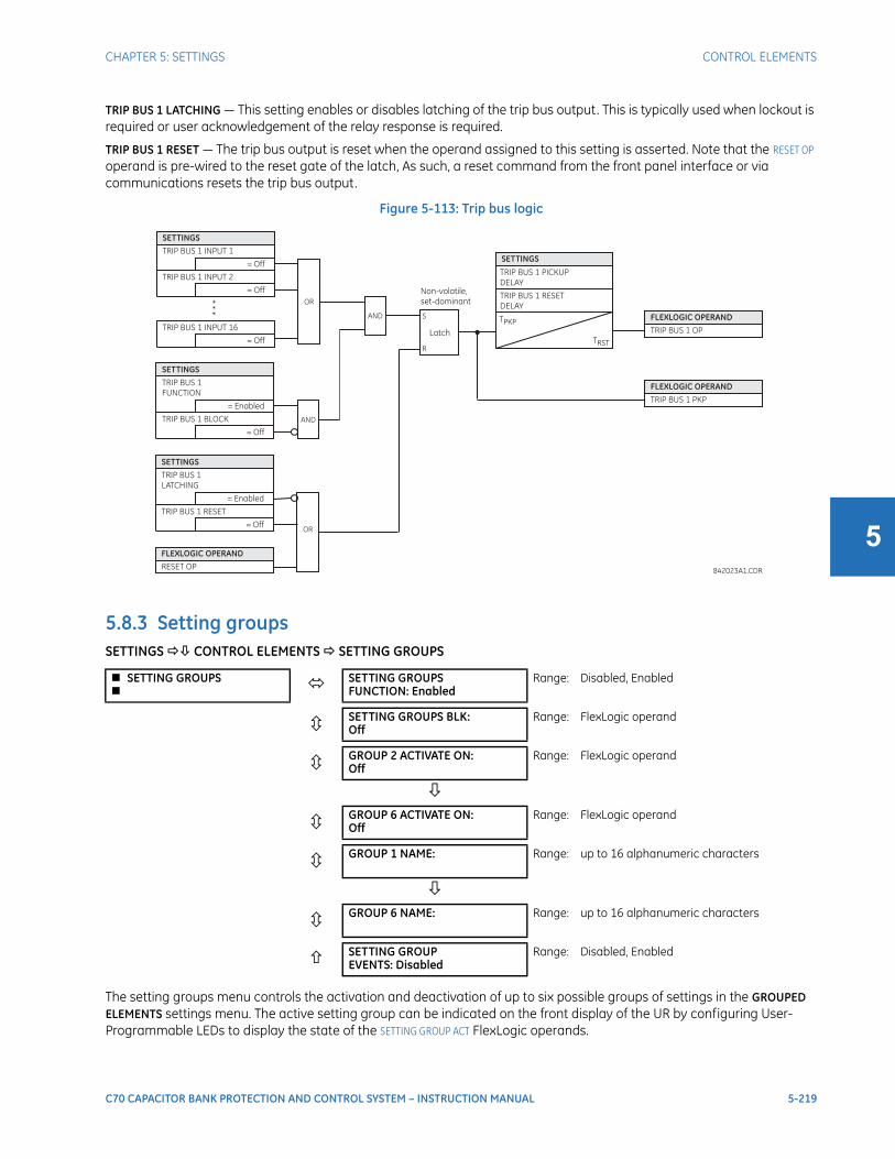
CHAPTER 5: SETTINGS CONTROL ELEMENTS
C70 CAPACITOR BANK PROTECTION AND CONTROL SYSTEM – INSTRUCTION MANUAL 5-219
5
TRIP BUS 1 LATCHING — This setting enables or disables latching of the trip bus output. This is typically used when lockout is required or user acknowledgement of the relay response is required.
TRIP BUS 1 RESET — The trip bus output is reset when the operand assigned to this setting is asserted. Note that the RESET OP operand is pre-wired to the reset gate of the latch, As such, a reset command from the front panel interface or via communications resets the trip bus output.
Figure 5-113: Trip bus logic
5.8.3 Setting groupsSETTINGS CONTROL ELEMENTS SETTING GROUPS
The setting groups menu controls the activation and deactivation of up to six possible groups of settings in the GROUPED ELEMENTS settings menu. The active setting group can be indicated on the front display of the UR by configuring User-Programmable LEDs to display the state of the SETTING GROUP ACT FlexLogic operands.
SETTING GROUPS SETTING GROUPS
FUNCTION: EnabledRange: Disabled, Enabled
SETTING GROUPS BLK:Off
Range: FlexLogic operand
GROUP 2 ACTIVATE ON:Off
Range: FlexLogic operand
GROUP 6 ACTIVATE ON:Off
Range: FlexLogic operand
GROUP 1 NAME: Range: up to 16 alphanumeric characters
GROUP 6 NAME: Range: up to 16 alphanumeric characters
SETTING GROUPEVENTS: Disabled
Range: Disabled, Enabled
**
*
SETTINGS
= Off
TRIP BUS 1 INPUT 2
= Off
TRIP BUS 1 INPUT 1
= Off
TRIP BUS 1 INPUT 16
OR
SETTINGS
= Enabled
TRIP BUS 1
FUNCTION
= Off
TRIP BUS 1 BLOCK AND
AND
Latch
S
R
Non-volatile,
set-dominant
SETTINGS
= Enabled
TRIP BUS 1
LATCHING
= Off
TRIP BUS 1 RESET
FLEXLOGIC OPERAND
TRIP BUS 1 PKP
OR
SETTINGS
TRIP BUS 1 PICKUP
DELAY
TRIP BUS 1 RESET
DELAY
TPKP
TRST
FLEXLOGIC OPERAND
RESET OP
FLEXLOGIC OPERAND
TRIP BUS 1 OP
842023A1.CDR
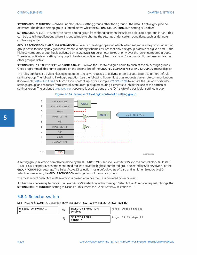
5-220 C70 CAPACITOR BANK PROTECTION AND CONTROL SYSTEM – INSTRUCTION MANUAL
CONTROL ELEMENTS CHAPTER 5: SETTINGS
5
SETTING GROUPS FUNCTION — When Enabled, allows setting groups other than group 1 (the default active group) to be activated. The default setting group is forced active while the SETTING GROUPS FUNCTION setting is Disabled.
SETTING GROUPS BLK — Prevents the active setting group from changing when the selected FlexLogic operand is "On." This can be useful in applications where it is undesirable to change the settings under certain conditions, such as during a control sequence.
GROUP 2 ACTIVATE ON to GROUP 6 ACTIVATE ON — Selects a FlexLogic operand which, when set, makes the particular setting group active for use by any grouped element. A priority scheme ensures that only one group is active at a given time — the highest-numbered group that is activated by its ACTIVATE ON parameter takes priority over the lower-numbered groups. There is no activate on setting for group 1 (the default active group), because group 1 automatically becomes active if no other group is active.
SETTING GROUP 1 NAME to SETTING GROUP 6 NAME — Allows the user to assign a name to each of the six settings groups. Once programmed, this name appears on the second line of the GROUPED ELEMENTS SETTING GROUP 1(6) menu display.
The relay can be set up via a FlexLogic equation to receive requests to activate or de-activate a particular non-default settings group. The following FlexLogic equation (see the following figure) illustrates requests via remote communications (for example, VIRTUAL INPUT 1 ON) or from a local contact input (for example, CONTACT IP 1 ON) to initiate the use of a particular settings group, and requests from several overcurrent pickup measuring elements to inhibit the use of the particular settings group. The assigned VIRTUAL OUTPUT 1 operand is used to control the “On” state of a particular settings group.
Figure 5-114: Example of FlexLogic control of a setting group
A setting group selection can also be made by the IEC 61850 MMS service SelectActiveSG to the control block @Master/LLN0.SGCB. The priority scheme mentioned makes active the highest numbered group selected by SelectActiveSG or the GROUP ACTIVATE ON settings. The SelectActiveSG selection has a default value of 1, so until a higher SelectActiveSG selection is received, the GROUP ACTIVATE ON settings control the active group.
The most recent SelectActiveSG selection is preserved while the UR is powered down or reset.
If it becomes necessary to cancel the SelectActiveSG selection without using a SelectActiveSG service request, change the SETTING GROUPS FUNCTION setting to Disabled. This resets the SelectActiveSG selection to 1.
5.8.4 Selector switchSETTINGS CONTROL ELEMENTS SELECTOR SWITCH SELECTOR SWITCH 1(2)
SELECTOR SWITCH 1 SELECTOR 1 FUNCTION:
DisabledRange: Disabled, Enabled
SELECTOR 1 FULLRANGE: 7
Range: 1 to 7 in steps of 1
10
1 VIRT IP 1 ON (VI1)
2 CONT IP 1 ON (H5A)
3
OR (2)
OR (2)
4 PHASE TOC1 PKP
5 NOT
6 PHASE TOC2 PKP
7 NOT
8
AND (3)
AND (3)
9
= VIRT OP 1 (VO1)
= VIRT OP 1 (VO1)
END842789A1.CDR

CHAPTER 5: SETTINGS CONTROL ELEMENTS
C70 CAPACITOR BANK PROTECTION AND CONTROL SYSTEM – INSTRUCTION MANUAL 5-221
5The selector switch element is intended to replace a mechanical selector switch. Typical applications include setting group control or control of multiple logic sub-circuits in user-programmable logic.
The element provides for two control inputs. The step-up control allows stepping through selector position one step at a time with each pulse of the control input, such as a user-programmable pushbutton. The three-bit control input allows setting the selector to the position defined by a three-bit word.
The element allows pre-selecting a new position without applying it . The pre-selected position gets applied either after time-out or upon acknowledgement via separate inputs (user setting). The selector position is stored in non-volatile memory. Upon power-up, either the previous position is restored or the relay synchronizes to the current three-bit word (user setting). Basic alarm functionality alerts the user under abnormal conditions; for example, the three-bit control input being out of range.
A selector switch runs every two power cycles.
SELECTOR 1 FULL RANGE — This setting defines the upper position of the selector. When stepping up through available positions of the selector, the upper position wraps up to the lower position (position 1). When using a direct three-bit control word for programming the selector to a desired position, the change would take place only if the control word is within the range of 1 to the SELECTOR FULL RANGE. If the control word is outside the range, an alarm is established by setting the SELECTOR ALARM FlexLogic operand for three seconds.
SELECTOR 1 TIME-OUT — This setting defines the time-out period for the selector. This value is used by the relay in the following two ways. When the SELECTOR STEP-UP MODE is “Time-out,” the setting specifies the required period of inactivity of the control input after which the pre-selected position is automatically applied. When the SELECTOR STEP-UP MODE is “Acknowledge,” the setting specifies the period of time for the acknowledging input to appear. The timer is re-started by any activity of the control input. The acknowledging input must come before the SELECTOR 1 TIME-OUT timer expires; otherwise, the change does not take place and an alarm is set.
SELECTOR 1 STEP-UP — This setting specifies a control input for the selector switch. The switch is shifted to a new position at each rising edge of this signal. The position changes incrementally, wrapping up from the last (SELECTOR 1 FULL RANGE) to the first (position 1). Consecutive pulses of this control operand must not occur faster than every 50 ms. After each rising edge of the assigned operand, the time-out timer is restarted and the SELECTOR SWITCH 1: POS Z CHNG INITIATED target
SELECTOR 1 TIME-OUT:5.0 s
Range: 3.0 to 60.0 s in steps of 0.1
SELECTOR 1 STEP-UP:Off
Range: FlexLogic operand
SELECTOR 1 STEP-UPMODE: Time-out
Range: Time-out, Acknowledge
SELECTOR 1 ACK:Off
Range: FlexLogic operand
SELECTOR 1 3BIT A0:Off
Range: FlexLogic operand
SELECTOR 1 3BIT A1:Off
Range: FlexLogic operand
SELECTOR 1 3BIT A2:Off
Range: FlexLogic operand
SELECTOR 1 3BITMODE: Time-out
Range: Time-out, Acknowledge
SELECTOR 1 3BIT ACK:Off
Range: FlexLogic operand
SELECTOR 1 POWER-UPMODE: Restore
Range: Restore, Synchronize, Sync/Restore
SELECTOR 1 TARGETS:Self-reset
Range: Self-reset, Latched, Disabled
SELECTOR 1 EVENTS:Disabled
Range: Disabled, Enabled

5-222 C70 CAPACITOR BANK PROTECTION AND CONTROL SYSTEM – INSTRUCTION MANUAL
CONTROL ELEMENTS CHAPTER 5: SETTINGS
5
message is displayed, where Z the pre-selected position. The message is displayed for the time specified by the FLASH MESSAGE TIME setting. The pre-selected position is applied after the selector times out (“Time-out” mode), or when the acknowledging signal appears before the element times out (“Acknowledge” mode). When the new position is applied, the relay displays the SELECTOR SWITCH 1: POSITION Z IN USE message. Typically, a user-programmable pushbutton is configured as the stepping up control input.
SELECTOR 1 STEP-UP MODE — This setting defines the selector mode of operation. When set to “Time-out,” the selector changes its position after a pre-defined period of inactivity at the control input. The change is automatic and does not require any explicit confirmation of the intent to change the selector's position. When set to “Acknowledge,” the selector changes its position only after the intent is confirmed through a separate acknowledging signal. If the acknowledging signal does not appear within a pre-defined period of time, the selector does not accept the change and an alarm is established by setting the SELECTOR STP ALARM output FlexLogic operand for three seconds.
SELECTOR 1 ACK — This setting specifies an acknowledging input for the stepping up control input. The pre-selected position is applied on the rising edge of the assigned operand. This setting is active only under “Acknowledge” mode of operation. The acknowledging signal must appear within the time defined by the SELECTOR 1 TIME-OUT setting after the last activity of the control input. A user-programmable pushbutton is typically configured as the acknowledging input.
SELECTOR 1 3BIT A0, A1, and A2 — These settings specify a three-bit control input of the selector. The three-bit control word pre-selects the position using the following encoding convention:
The “rest” position (0, 0, 0) does not generate an action and is intended for situations when the device generating the three-bit control word is having a problem. When SELECTOR 1 3BIT MODE is “Time-out,” the pre-selected position is applied in SELECTOR 1 TIME-OUT seconds after the last activity of the three-bit input. When SELECTOR 1 3BIT MODE is “Acknowledge,” the pre-selected position is applied on the rising edge of the SELECTOR 1 3BIT ACK acknowledging input.
The stepping up control input (SELECTOR 1 STEP-UP) and the three-bit control inputs (SELECTOR 1 3BIT A0 through A2) lock-out mutually: once the stepping up sequence is initiated, the three-bit control input is inactive; once the three-bit control sequence is initiated, the stepping up input is inactive.
SELECTOR 1 3BIT MODE — This setting defines the selector mode of operation. When set to “Time-out,” the selector changes its position after a pre-defined period of inactivity at the control input. The change is automatic and does not require explicit confirmation to change the selector position. When set to “Acknowledge,” the selector changes its position only after confirmation via a separate acknowledging signal. If the acknowledging signal does not appear within a pre-defined period of time, the selector rejects the change and an alarm established by invoking the SELECTOR BIT ALARM FlexLogic operand for three seconds.
SELECTOR 1 3BIT ACK — This setting specifies an acknowledging input for the three-bit control input. The pre-selected position is applied on the rising edge of the assigned FlexLogic operand. This setting is active only under the “Acknowledge” mode of operation. The acknowledging signal must appear within the time defined by the SELECTOR TIME-OUT setting after the last activity of the three-bit control inputs. Note that the stepping up control input and three-bit control input have independent acknowledging signals (SELECTOR 1 ACK and SELECTOR 1 3BIT ACK, accordingly).
SELECTOR 1 POWER-UP MODE — This setting specifies the element behavior on power up of the relay.
When set to “Restore,” the last position of the selector (stored in the non-volatile memory) is restored after powering up the relay. If the position restored from memory is out of range, position 0 (no output operand selected) is applied and an alarm is set (SELECTOR 1 PWR ALARM).
A2 A1 A0 Position
0 0 0 rest
0 0 1 1
0 1 0 2
0 1 1 3
1 0 0 4
1 0 1 5
1 1 0 6
1 1 1 7
CHAPTER 5: SETTINGS CONTROL ELEMENTS
C70 CAPACITOR BANK PROTECTION AND CONTROL SYSTEM – INSTRUCTION MANUAL 5-223
5
When set to “Synchronize,” the selector switch acts as follows. For two power cycles, the selector applies position 0 to the switch and activates SELECTOR 1 PWR ALARM. After two power cycles expire, the selector synchronizes to the position dictated by the three-bit control input. This operation does not wait for time-out or the acknowledging input. When the synchronization attempt is unsuccessful (that is, the three-bit input is not available (0,0,0) or out of range), then the selector switch output is set to position 0 (no output operand selected) and an alarm is established (SELECTOR 1 PWR ALARM).
The operation of “Synch/Restore” mode is similar to the “Synchronize” mode. The only difference is that after an unsuccessful synchronization attempt, the switch attempts to restore the position stored in the relay memory. The “Synch/Restore” mode is useful for applications where the selector switch is employed to change the setting group in redundant (two relay) protection schemes.
SELECTOR 1 EVENTS — If enabled, the following events are logged:
The following figures illustrate the operation of the selector switch. In these diagrams, “T” represents a time-out setting.
Event name Description
SELECTOR 1 POS Z Selector 1 changed its position to Z
SELECTOR 1 STP ALARM The selector position pre-selected via the stepping up control input has not been confirmed before the time out
SELECTOR 1 BIT ALARM The selector position pre-selected via the three-bit control input has not been confirmed before the time out

5-224 C70 CAPACITOR BANK PROTECTION AND CONTROL SYSTEM – INSTRUCTION MANUAL
CONTROL ELEMENTS CHAPTER 5: SETTINGS
5
Figure 5-115: Time-out mode
842737A1.CDR
STEP-UP
3BIT A0
3BIT A1
3BIT A2
POS 1
POS 2
POS 3
POS 4
POS 5
POS 6
POS 7
BIT 0
BIT 1
BIT 2
pre-existing
position 2
changed to 4 with
a pushbutton
changed to 1 with
a 3-bit input
changed to 2 with a
pushbutton
T T
T T
changed to 7 with
a 3-bit input
STP ALARM
BIT ALARM
ALARM
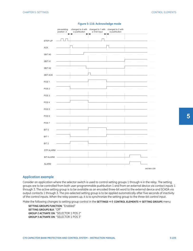
CHAPTER 5: SETTINGS CONTROL ELEMENTS
C70 CAPACITOR BANK PROTECTION AND CONTROL SYSTEM – INSTRUCTION MANUAL 5-225
5
Figure 5-116: Acknowledge mode
Application exampleConsider an application where the selector switch is used to control setting groups 1 through 4 in the relay. The setting groups are to be controlled from both user-programmable pushbutton 1 and from an external device via contact inputs 1 through 3. The active setting group is to be available as an encoded three-bit word to the external device and SCADA via output contacts 1 through 3. The pre-selected setting group is to be applied automatically after five seconds of inactivity of the control inputs. When the relay powers up, it is to synchronize the setting group to the three-bit control input.
Make the following changes to setting group control in the SETTINGS CONTROL ELEMENTS SETTING GROUPS menu:SETTING GROUPS FUNCTION: “Enabled”SETTING GROUPS BLK: “Off”GROUP 2 ACTIVATE ON: “SELECTOR 1 POS 2"GROUP 3 ACTIVATE ON: “SELECTOR 1 POS 3"
842736A1.CDR
STEP-UP
ACK
3BIT A0
3BIT A1
3BIT A2
3BIT ACK
POS 1
POS 2
POS 3
POS 4
POS 5
POS 6
POS 7
BIT 0
BIT 1
BIT 2
pre-existing
position 2
changed to 4 with
a pushbutton
changed to 1 with
a 3-bit input
changed to 2 with
a pushbutton
STP ALARM
BIT ALARM
ALARM

5-226 C70 CAPACITOR BANK PROTECTION AND CONTROL SYSTEM – INSTRUCTION MANUAL
CONTROL ELEMENTS CHAPTER 5: SETTINGS
5
GROUP 4 ACTIVATE ON: “SELECTOR 1 POS 4"GROUP 5 ACTIVATE ON: “Off”GROUP 6 ACTIVATE ON: “Off”
Make the following changes to selector switch element in the SETTINGS CONTROL ELEMENTS SELECTOR SWITCH SELECTOR SWITCH 1 menu to assign control to user programmable pushbutton 1 and contact inputs 1 through 3:
SELECTOR 1 FUNCTION: “Enabled”SELECTOR 1 FULL-RANGE: “4”SELECTOR 1 STEP-UP MODE: “Time-out”SELECTOR 1 TIME-OUT: “5.0 s”SELECTOR 1 STEP-UP: “PUSHBUTTON 1 ON”SELECTOR 1 ACK: “Off”SELECTOR 1 3BIT A0: “CONT IP 1 ON”SELECTOR 1 3BIT A1: “CONT IP 2 ON”SELECTOR 1 3BIT A2: “CONT IP 3 ON”SELECTOR 1 3BIT MODE: “Time-out”SELECTOR 1 3BIT ACK: “Off”SELECTOR 1 POWER-UP MODE: “Synchronize”
Now, assign the contact output operation (assume the H6E module) to the selector switch element by making the following changes in the SETTINGS INPUTS/OUTPUTS CONTACT OUTPUTS menu:
OUTPUT H1 OPERATE: “SELECTOR 1 BIT 0"OUTPUT H2 OPERATE: “SELECTOR 1 BIT 1"OUTPUT H3 OPERATE: “SELECTOR 1 BIT 2"
Finally, assign configure user-programmable pushbutton 1 by making the following changes in the SETTINGS PRODUCT SETUP USER-PROGRAMMABLE PUSHBUTTONS USER PUSHBUTTON 1 menu:
PUSHBUTTON 1 FUNCTION: “Self-reset”PUSHBUTTON 1 DROP-OUT TIME: “0.10 s”
The figure shows the logic for the selector switch.
Figure 5-117: Selector switch logic
842012A2.CDR
step up
acknowledge
3-bit position out
ON
FLEXLOGIC™ OPERANDS
SELECTOR 1 POS 1
SELECTOR 1 POS 2
SELECTOR 1 POS 3
SELECTOR 1 POS 4
SELECTOR 1 POS 5
SELECTOR 1 POS 6
SELECTOR 1 POS 7
SELECTOR 1 STP ALARM
SELECTOR 1 BIT ALARM
SELECTOR 1 ALARM
SELECTOR 1 BIT 0
SELECTOR 1 BIT 1
SELECTOR 1 BIT 2
FLEXLOGIC™ OPERANDS
RUN
SELECTOR 1 POWER-UP MODE:
SETTINGS
SELECTOR 1 TIME-OUT:
SELECTOR 1 STEP-UP MODE:
SELECTOR 1 FULL RANGE:
SELECTOR 1 STEP-UP:
Off = 0
SELECTOR 1 FUNCTION:
SETTINGS
Enabled = 1
SELECTOR 1 ACK:
Off = 0
SELECTOR 1 3BIT A0:
Off = 0
SELECTOR 1 3BIT A1:
Off = 0
SELECTOR 1 3BIT A2:
Off = 0
SELECTOR 1 3BIT ACK:
Off = 0 3-bit acknowledge
SELECTOR 1 POSITION
ACTUAL VALUE
21
3
4
5
6
7
SELECTOR 1 3BIT MODE:
SELECTOR 1 PWR ALARM
thre
e-b
itc
on
tro
lin
pu
t
OR
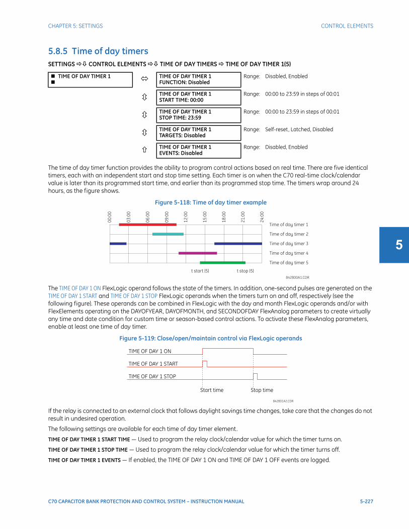
CHAPTER 5: SETTINGS CONTROL ELEMENTS
C70 CAPACITOR BANK PROTECTION AND CONTROL SYSTEM – INSTRUCTION MANUAL 5-227
5
5.8.5 Time of day timersSETTINGS CONTROL ELEMENTS TIME OF DAY TIMERS TIME OF DAY TIMER 1(5)
The time of day timer function provides the ability to program control actions based on real time. There are five identical timers, each with an independent start and stop time setting. Each timer is on when the C70 real-time clock/calendar value is later than its programmed start time, and earlier than its programmed stop time. The timers wrap around 24 hours, as the figure shows.
Figure 5-118: Time of day timer example
The TIME OF DAY 1 ON FlexLogic operand follows the state of the timers. In addition, one-second pulses are generated on the TIME OF DAY 1 START and TIME OF DAY 1 STOP FlexLogic operands when the timers turn on and off, respectively (see the following figure). These operands can be combined in FlexLogic with the day and month FlexLogic operands and/or with FlexElements operating on the DAYOFYEAR, DAYOFMONTH, and SECONDOFDAY FlexAnalog parameters to create virtually any time and date condition for custom time or season-based control actions. To activate these FlexAnalog parameters, enable at least one time of day timer.
Figure 5-119: Close/open/maintain control via FlexLogic operands
If the relay is connected to an external clock that follows daylight savings time changes, take care that the changes do not result in undesired operation.
The following settings are available for each time of day timer element.
TIME OF DAY TIMER 1 START TIME — Used to program the relay clock/calendar value for which the timer turns on.
TIME OF DAY TIMER 1 STOP TIME — Used to program the relay clock/calendar value for which the timer turns off.
TIME OF DAY TIMER 1 EVENTS — If enabled, the TIME OF DAY 1 ON and TIME OF DAY 1 OFF events are logged.
TIME OF DAY TIMER 1 TIME OF DAY TIMER 1
FUNCTION: DisabledRange: Disabled, Enabled
TIME OF DAY TIMER 1START TIME: 00:00
Range: 00:00 to 23:59 in steps of 00:01
TIME OF DAY TIMER 1STOP TIME: 23:59
Range: 00:00 to 23:59 in steps of 00:01
TIME OF DAY TIMER 1TARGETS: Disabled
Range: Self-reset, Latched, Disabled
TIME OF DAY TIMER 1EVENTS: Disabled
Range: Disabled, Enabled
842800A1.CDR
24
:00
21
:00
18
:00
15
:00
12
:00
09
:00
06
:00
03
:00
00
:00
Time of day timer 2
t start (5) t stop (5)
Time of day timer 1
Time of day timer 3
Time of day timer 4
Time of day timer 5
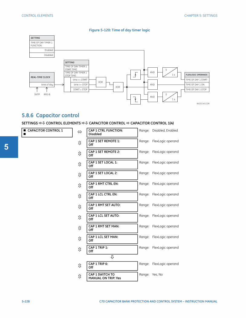
5-228 C70 CAPACITOR BANK PROTECTION AND CONTROL SYSTEM – INSTRUCTION MANUAL
CONTROL ELEMENTS CHAPTER 5: SETTINGS
5
Figure 5-120: Time of day timer logic
5.8.6 Capacitor controlSETTINGS CONTROL ELEMENTS CAPACITOR CONTROL CAPACITOR CONTROL 1(4)
CAPACITOR CONTROL 1 CAP 1 CTRL FUNCTION:
DisabledRange: Disabled, Enabled
CAP 1 SET REMOTE 1:Off
Range: FlexLogic operand
CAP 1 SET REMOTE 2:Off
Range: FlexLogic operand
CAP 1 SET LOCAL 1:Off
Range: FlexLogic operand
CAP 1 SET LOCAL 2:Off
Range: FlexLogic operand
CAP 1 RMT CTRL EN:Off
Range: FlexLogic operand
CAP 1 LCL CTRL EN:Off
Range: FlexLogic operand
CAP 1 RMT SET AUTO:Off
Range: FlexLogic operand
CAP 1 LCL SET AUTO:Off
Range: FlexLogic operand
CAP 1 RMT SET MAN:Off
Range: FlexLogic operand
CAP 1 LCL SET MAN:Off
Range: FlexLogic operand
CAP 1 TRIP 1:Off
Range: FlexLogic operand
CAP 1 TRIP 6:Off
Range: FlexLogic operand
CAP 1 SWITCH TOMANUAL ON TRIP: Yes
Range: Yes, No
842021A1.CDR
SETTING
TIME OF DAY TIMER 1
FUNCTION:
Enabled
Disabled
REAL-TIME CLOCK
time of day
SNTP IRIG-B
SETTING
TIME OF DAY TIMER 1
START TIME:
TIME OF DAY TIMER 1
STOP TIME:
time >= START
time >= STOP
START > STOP
XOR
XOR
AND
AND
0
1 s
0
1 s
FLEXLOGIC OPERANDS
TIME OF DAY 1 START
TIME OF DAY 1 ON
TIME OF DAY 1 STOP
AND

CHAPTER 5: SETTINGS CONTROL ELEMENTS
C70 CAPACITOR BANK PROTECTION AND CONTROL SYSTEM – INSTRUCTION MANUAL 5-229
5
The capacitor control element gathers on/off commands from various sources and executes them, while maintaining remote/local and auto/manual control rights. Local control refers to control from the front panel of the relay. Remote control refers to control via communications from outside of the relay, an on-site interface, and/or from an off-site control center. There is flexibility to support other configurations.
This element provides a user-programmable time delay that inhibits closing after the bank has been switched out of service until the bank has had time to discharge any trapped charge. If the capacitor were to be closed with trapped charge of opposite polarity from the system voltage at that instant, larger than normal transients would occur. A FlexAnalog value is available to inform the time remaining before the next permissible close operation.
Seal-in is provided to stretch short input commands to lengths suitable for breaker control. An interlock prevents simultaneous trip and close output, which can result in breaker pumping. To prevent a continuous close input from causing reclosing of the breaker following a trip command, the interlock is sealed-in for the duration of any close input.
A provision is provided to force the auto/manual mode to manual on protection operation. This prevents the capacitor automatic switching scheme from attempting to close a faulted capacitor. A setting controls the automatic switchover to manual upon the protection trip.
CAP 1 AUTO CTRL EN:Off
Range: FlexLogic operand
CAP 1 LOCAL OPEN:Off
Range: FlexLogic operand
CAP 1 AUTO OPEN:Off
Range: FlexLogic operand
CAP 1 BKR OPEN 52b:Off
Range: FlexLogic operand
CAP 1 TRIP SEAL-INDELAY: 0.400 s
Range: 0.000 to 60.000 s in steps of 0.001
CAP 1 REMOTE CLOSE:Off
Range: FlexLogic operand
CAP 1 LOCAL CLOSE:Off
Range: FlexLogic operand
CAP 1 AUTO CLOSE:Off
Range: FlexLogic operand
CAP 1 BKR CLSD 52a:Off
Range: FlexLogic operand
CAP 1 DISCHARGEDELAY: 300 s
Range: 0 to 3600 s in steps of 1
CAP 1 CLOSE SEAL-INDELAY: 0.400 s
Range: 0.000 to 60.000 s in steps of 0.001
CAP 1 BKR CLOSE BLK:Off
Range: FlexLogic operand
CAP 1 CLS OVERRIDE:Off
Range: FlexLogic operand
CAP 1 TARGETS:Disabled
Range: Self-reset, Latched, Disabled
CAP 1 EVENTS:Disabled
Range: Disabled, Enabled
The C70 is provided with optional capacity bank control. This feature is specified as an option at the time of ordering. See the Order Codes section in chapter 2 for details.
5-230 C70 CAPACITOR BANK PROTECTION AND CONTROL SYSTEM – INSTRUCTION MANUAL
CONTROL ELEMENTS CHAPTER 5: SETTINGS
5
The following settings are available for each capacitor control element.
CAP 1 CTRL FUNCTION — This setting is used to enable the element. When disabled, the remote/local latch is forced to local, the auto/manual latch is forced to manual, the trip and close command outputs are forced off, and their seal-in latches and timers are reset.
CAP 1 SET REMOTE 1(2) — Sets one or two FlexLogic operands to select the remote mode. It is expected that one of these settings is programmed to a pushbutton “on” operand. This allows a local operator to hand over control to remote operators. Where appropriate, the other one of these settings can be set to a virtual input. This allows remote operators to grant themselves control rights.
CAP 1 SET LOCAL 1(2) — Similar to previous setting, but selects local mode.
CAP 1 RMT CTRL EN — Selects a FlexLogic operand to enable remote auto/manual and open/close control. It is expected to be set to CAP 1 IN REMOTE to obtain the baseline functionality, but variations via FlexLogic are possible. For example, if it is required that remote control is always available, this setting can be set to “On.”
CAP 1 LCL CTRL EN — Similar to previous setting, but enables local controls. Expected to be set to CAP 1 IN LOCAL.
CAP 1 RMT SET AUTO — Selects a FlexLogic operand that selects auto mode when remote control is enabled. It is expected to be set to a virtual input to enables HMI/SCADA access via one of the supported protocols.
CAP 1 LCL SET AUTO — Similar to previous setting, but expected to be set to a pushbutton “on” operand.
CAP 1 RMT SET MAN — Similar to the CAP RMT SET AUTO setting, but selects manual mode.
CAP 1 LCL SET MAN — Similar to the CAP LCL SET AUTO setting, but selects manual mode.
CAP 1 TRIP 1(6) — Selects up to six FlexLogic operands to activate the CAP 1 BKR TRIP operand, no matter what control modes prevail. Expected to be set to the appropriate protection element operate operand.
CAP 1 SWITCH TO MANUAL ON TRIP — Allows control of the auto/manual mode when issuing a trip command. When set to “Yes,” the element switches to manual mode upon tripping the bank from protection.
CAP 1 AUTO CTRL EN — Selects a FlexLogic operand to enable automatic open/close control. It is expected to be set to CAP 1 IN AUTO to obtain the baseline functionality, but variations are possible.
CAP 1 MAN CTRL EN — Similar to previous setting, but enables manual controls. Expected to be set to CAP 1 IN MAN.
CAP 1 REMOTE OPEN — Selects a FlexLogic operand to activate the CAP 1 BKR TRIP operand when both remote and manual control are enabled. It is expected to be set to a virtual input, and that the contact output wired to the capacitor breaker trip coil is set to CAP 1 BKR TRIP.
CAP 1 LOCAL OPEN — Similar to previous setting, but requires both local and manual control to be enabled. Expected to be set to a pushbutton “on” operand.
CAP 1 AUTO OPEN — Similar to previous setting, but requires automatic control to be enabled. Expected to be set to the open command of the voltage regulator either built-in or customer via FlexLogic.
CAP 1 BKR OPEN 52b — Selects a FlexLogic operand that cancels the trip seal-in. Expected to be set to the contact input to which a contact is wired that is closed when the capacitor breaker is open. When both 52a and 52b contacts are used for security, the appropriate filtering logic possibly including discrepancy alarming can be programmed in FlexLogic, and the resulting virtual output can be configured under this setting.
CAP 1 TRIP SEAL-IN DELAY — Sets a maximum trip seal-in duration for where the CAP 1 BKR OPEN 52b setting is not configured or fails to operate.
CAP 1 REMOTE CLOSE — Similar to the CAP 1 REMOTE OPEN setting, but closes the breaker.
CAP 1 LOCAL CLOSE — Similar to the CAP 1 LOCAL OPEN setting, but closes the breaker.
CAP 1 AUTO CLOSE — Similar to the CAP 1 AUTO OPEN setting, but closes the breaker.
CAP 1 BKR CLSD 52a — Similar to the CAP 1 BKR OPEN 52b setting, but cancels the close seal-in, and is expected to be set to a contact that is closed when the breaker is closed. The selected operand also triggers the CAP 1 DISCHARGE TIME. When both 52a and 52b contacts are used for security, the appropriate filtering logic possibly including discrepancy alarming can be programmed in FlexLogic, and the resulting virtual output can be configured under this setting.
CAP 1 CLOSE SEAL-IN DELAY — Sets a maximum close seal-in duration for where the CAP BKR CLSD 52a setting is not configured or fails to operate.

CHAPTER 5: SETTINGS CONTROL ELEMENTS
C70 CAPACITOR BANK PROTECTION AND CONTROL SYSTEM – INSTRUCTION MANUAL 5-231
5
CAP 1 DISCHARGE TIME — Sets a time delay that inhibits closing after the bank has been switched out-of-service (the CAP BKR CLSD 52a setting goes low or trip command terminates) until the bank has had time to discharge any trapped charge. The correct value for this setting depends on the specifics of the capacitor installation.
CAP 1 BKR CLOSE BLK — Selects a FlexLogic operand that triggers the CAP 1 BKR CLOSE interlock logic. Its signal is expected to originate from capacitor breaker trips external to the relay, and thus not otherwise able to block relay closing (for example, from the opposite group's capacitor protection).
CAP 1 CLS OVERRIDE — Selects a FlexLogic operand that overrides all inhibits for the breaker close command and allows the CLOSE command to be issued from any source as per the logic diagram.

5-232 C70 CAPACITOR BANK PROTECTION AND CONTROL SYSTEM – INSTRUCTION MANUAL
CONTROL ELEMENTS CHAPTER 5: SETTINGS
5
Figure 5-121: Capacitor bank control logic
FLEXLOGIC OPERAND
CAP 1 IN LOCALCAP 1 IN REMOTES
R
SETTINGS
CAP 1 SET LOCAL 1
OR
OR
CAP 1 SET REMOTE 1
CAP 1 SET REMOTE 2
CAP 1 LCL CTRL EN
CAP 1 RMT CTRL EN
CAP 1 AUTO CTRL EN
CAP 1 MAN CTRL EN
AND
AND
AND
OR
OR
S
R
FLEXLOGIC OPERANDCAP 1 IN AUTOCAP 1 IN MAN
CAP 1 LCL SET AUTO
CAP 1 RMT SET AUTO
CAP 1 LCL SET MAN
CAP 1 RMT SET MAN
AND
AND
AND
ORSETTINGS
CAP 1 LOCAL OPEN
CAP 1 REMOTE OPEN
CAP 1 TRIP 1
CAP 1 TRIP 2
CAP 1 TRIP 3
CAP 1 TRIP 4
CAP 1 TRIP 5
CAP 1 TRIP 6
CAP 1 AUTO OPEN
SETTINGS
AND
AND
AND
AND
SETTINGS
CAP 1 LOCAL CLOSE
CAP 1 REMOTE CLOSE
CAP 1 AUTO CLOSE
CAP 1 CLOSE SEAL-IN DELAYSETTINGS
0
OR
AND
CAP 1 TRIP SEAL-IN DELAYSETTINGS
0tPKP
tPKP
SETTINGSCAP 1 BKR OPEN 52b
CAP 1 BKR CLSD 52a
AND
CAP 1 DISCHARGE TIME: SETTINGS
tDPO
0OR
OR
AND
SETTINGSCAP 1 BKR CLOSE BLK
FLEXLOGIC OPERANDCAP 1 BKR TRIP
FLEXLOGIC OPERANDCAP 1 BKR CLOSE
SETTINGSCAP 1 CTRL FUNCTIONEnabled = 1
AND
AND
Reset DominantNon-Volatile Latch
Reset DominantNon-Volatile Latch
FLEXLOGIC OPERANDCAP 1 DISCHARGING
FLEXANALOGCAP 1 DISCHRG TIME
seconds remaining tillclosing is enabled
Reset
SETTINGS
OR
CAP 1 SWITCH TO MANUALON TRIP:
ANDYes = 1
SETTINGCAP 1 1 CLS OVERRIDE:Off = 0
OR
SETTINGS
SETTINGS
SETTINGS
AND
CAP 1 SET LOCAL 2
OFF = 0
OFF = 0
OFF = 0
OFF = 0
OFF = 0
OFF = 0
OFF = 0
OFF = 0
OFF = 0
OFF = 0
OFF = 0
OFF = 0
OFF = 0
OFF = 0
OFF = 0
OFF = 0
OFF = 0
OFF = 0
OFF = 0
OFF = 0
OFF = 0
OFF = 0
OFF = 0
OFF = 0
OFF = 0
OFF = 0
OFF = 0
834740A1.DWG
CHAPTER 5: SETTINGS CONTROL ELEMENTS
C70 CAPACITOR BANK PROTECTION AND CONTROL SYSTEM – INSTRUCTION MANUAL 5-233
5
5.8.7 Automatic voltage regulatorSETTINGS CONTROL ELEMENTS AUTOMATIC VOLTAGE REGULATOR AUTOMATIC VOLTAGE REGULATOR 1(3)
The automatic voltage regulator element (AVR) is intended to switch a static capacitor bank breaker open and closed to regulate system voltage, load voltage, power factor, or reactive power. The figure shows some applications.
AUTOMATIC VOLTAGE REGULATOR 1 AVR 1 FUNCTION:
DisabledRange: Disabled, Enabled
AVR 1 SOURCE:SRC 1
Range: SRC 1, SRC 2, SRC 3, SRC 4, SRC 5, SRC 6
AVR 1 MINIMUMVOLTAGE: 0.500 pu
Range: 0.500 to 1.500 pu in steps of 0.001
AVR 1 CONTROL MODE:Voltage
Range: Voltage, VAR
AVR 1 VOLT OPERATINGSIGNAL: V1
Range: Vab, Vbc, Vca, Vaver, V1, Vaux, Vag, Vbg, Vcg
AVR 1 VOLT LEVEL TOCLOSE: 0.950 pu
Range: 0.750 to 1.500 pu in steps of 0.001
AVR 1 VOLT LEVEL TOOPEN: 1.050 pu
Range: 0.750 to 1.500 pu in steps of 0.001
AVR 1 VOLT DROPCOMPENS Z: 0.00 Ω
Range: 0 to 250.00 ohms in steps of 0.01
AVR 1 VOLT DROPCOMPENS RCA: 75°
Range: 30 to 90° in steps of 1
AVR 1 VAR LEVEL TOCLOSE: 0.500 pu
Range: –1.500 to 1.500 pu in steps of 0.001
AVR 1 VAR LEVEL TOOPEN: -0.500 pu
Range: –1.500 to 1.500 pu in steps of 0.001
AVR 1 POWER FACTORLIMIT: 1.00
Range: 0.50 to 1.00 pu in steps of 0.01
AVR 1 VAR OPEN MODE:Minimize No. of Ops.
Range: Minimize Uptime, Minimize No. of Ops.
AVR 1 DELAY BEFORECLOSE: 1.000 s
Range: 0.000 to 65.353 s in steps of 0.001
AVR 1 DELAY BEFOREOPEN: 1.000 s
Range: 0.000 to 65.353 s in steps of 0.001
AVR 1 BLOCK:Off
Range: FlexLogic operand
AVR 1 TARGET:Self-reset
Range: Self-reset, Latched, Disabled
AVR 1 EVENTS:Disabled
Range: Disabled, Enabled

5-234 C70 CAPACITOR BANK PROTECTION AND CONTROL SYSTEM – INSTRUCTION MANUAL
CONTROL ELEMENTS CHAPTER 5: SETTINGS
5
Figure 5-122: Applications of the capacitor automatic voltage regulator function
Up to three identical automatic voltage regulator elements are provided, allowing the relay to be used with capacitor banks divided into sections for finer compensation steps, to provide switching speed dependant on the extent of the voltage or power deviation, or to provide different settings depending on a user-programmable factor such as time of day.
Each element can be set to operate in either “Voltage” mode or “VAR” mode. The voltage mode can be used with relatively short time delay settings as a system stability aid, or with longer time delay settings to assist in the regulation of steady state voltage. When the voltage decreases to the volts level to close setting, after the set close delay the capacitor is closed, raising the voltage. When the voltage increases to the level to open setting, after the set open delay the capacitor is opened, lowering the voltage. The load drop compensation feature can be used to effectively sense the voltage at a location remote from the relay.
The “VAR” mode can be used to regulate the var and power factor of a load to reduce transmission and distribution costs. If the capacitor deployment objective is to minimize system power losses, set the power factor limit to 1.000 to disable it and set the var open and close levels symmetrically about zero reactive power, with a difference between levels equal to the reactive power produced by the capacitor plus margin. Larger margins result in less frequent switching.
If on the other hand the deployment objective is solely to minimize power factor rate charges, set the power factor limit to the value at which power factor penalties are incurred, typically 0.9. Set the var close level to the vars that would flow should the power factor be at the limit when at the minimum expected kW demand. The open command characteristics can be selected to suit whether the preference is to minimize the amount of time the capacitor is online or to minimize the number of capacitor close operations. For the former preference, set the var open mode to “Minimize Uptime” and set the var open level below the close level by an amount equal to the capacitor var rating plus margin. For the latter preference, set the var open mode to “Minimize No. of Ops” (minimize number of operations) and set the var open level to the negative of the close level.
System
AVR
Load
a) System voltage regulation
System
AVR
Load
b) Load voltage regulation
feeder
impedance
System
AVR
Load
c) Load power factor regulation
System
AVR
Load
d) Load power factor regulation, alternate configuration
834731A1.CDR
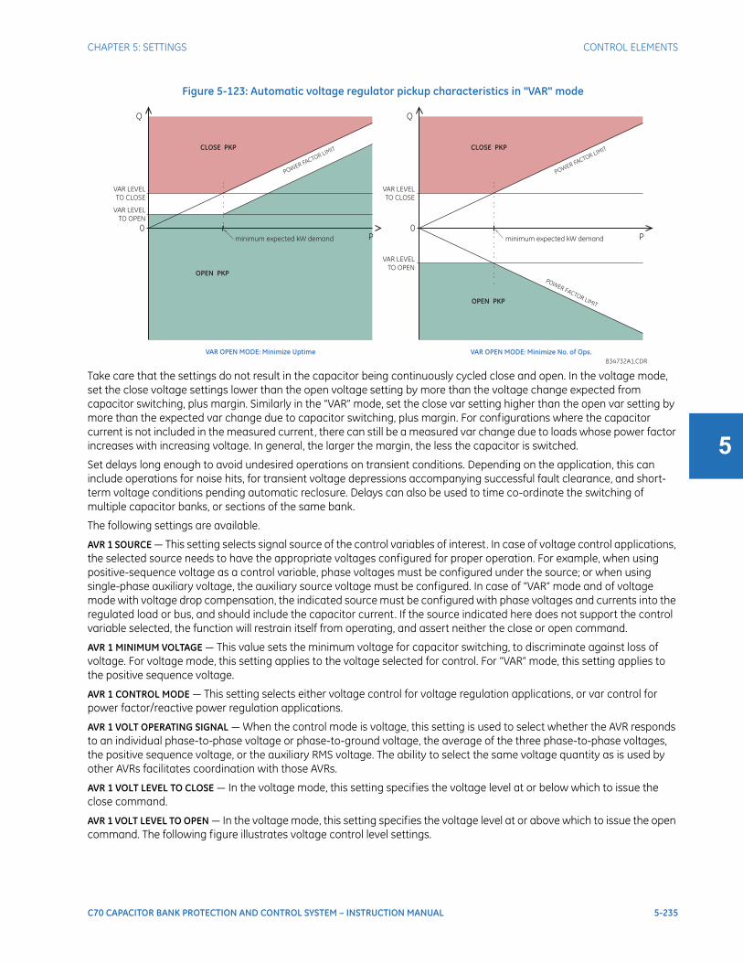
CHAPTER 5: SETTINGS CONTROL ELEMENTS
C70 CAPACITOR BANK PROTECTION AND CONTROL SYSTEM – INSTRUCTION MANUAL 5-235
5
Figure 5-123: Automatic voltage regulator pickup characteristics in "VAR" mode
Take care that the settings do not result in the capacitor being continuously cycled close and open. In the voltage mode, set the close voltage settings lower than the open voltage setting by more than the voltage change expected from capacitor switching, plus margin. Similarly in the “VAR” mode, set the close var setting higher than the open var setting by more than the expected var change due to capacitor switching, plus margin. For configurations where the capacitor current is not included in the measured current, there can still be a measured var change due to loads whose power factor increases with increasing voltage. In general, the larger the margin, the less the capacitor is switched.
Set delays long enough to avoid undesired operations on transient conditions. Depending on the application, this can include operations for noise hits, for transient voltage depressions accompanying successful fault clearance, and short-term voltage conditions pending automatic reclosure. Delays can also be used to time co-ordinate the switching of multiple capacitor banks, or sections of the same bank.
The following settings are available.
AVR 1 SOURCE — This setting selects signal source of the control variables of interest. In case of voltage control applications, the selected source needs to have the appropriate voltages configured for proper operation. For example, when using positive-sequence voltage as a control variable, phase voltages must be configured under the source; or when using single-phase auxiliary voltage, the auxiliary source voltage must be configured. In case of “VAR” mode and of voltage mode with voltage drop compensation, the indicated source must be configured with phase voltages and currents into the regulated load or bus, and should include the capacitor current. If the source indicated here does not support the control variable selected, the function will restrain itself from operating, and assert neither the close or open command.
AVR 1 MINIMUM VOLTAGE — This value sets the minimum voltage for capacitor switching, to discriminate against loss of voltage. For voltage mode, this setting applies to the voltage selected for control. For “VAR” mode, this setting applies to the positive sequence voltage.
AVR 1 CONTROL MODE — This setting selects either voltage control for voltage regulation applications, or var control for power factor/reactive power regulation applications.
AVR 1 VOLT OPERATING SIGNAL — When the control mode is voltage, this setting is used to select whether the AVR responds to an individual phase-to-phase voltage or phase-to-ground voltage, the average of the three phase-to-phase voltages, the positive sequence voltage, or the auxiliary RMS voltage. The ability to select the same voltage quantity as is used by other AVRs facilitates coordination with those AVRs.
AVR 1 VOLT LEVEL TO CLOSE — In the voltage mode, this setting specifies the voltage level at or below which to issue the close command.
AVR 1 VOLT LEVEL TO OPEN — In the voltage mode, this setting specifies the voltage level at or above which to issue the open command. The following figure illustrates voltage control level settings.
834732A1.CDR
Q
P
POWER FACTOR LIMIT
CLOSE PKP
OPEN PKP
0
VAR OPEN MODE: Minimize No. of Ops.
VAR LEVEL
TO CLOSE
VAR LEVEL
TO OPEN
Q
P
POWER FACTOR LIM
ITCLOSE PKP
0
OPEN PKP
VAR OPEN MODE: Minimize Uptime
minimum expected kW demand minimum expected kW demand
POWER FACTOR LIM
IT
VAR LEVEL
TO CLOSE
VAR LEVEL
TO OPEN

5-236 C70 CAPACITOR BANK PROTECTION AND CONTROL SYSTEM – INSTRUCTION MANUAL
CONTROL ELEMENTS CHAPTER 5: SETTINGS
5
Figure 5-124: Close and open levels when controlling voltage or VARs
AVR 1 VOLT DROP COMPENS Z — In the voltage mode, this setting allows compensating for voltage drop on the line when the relay measuring point is located upstream of the load. Positive-sequence line impedance is entered in secondary ohms. Compensation cannot exceed 20% of the nominal phase voltage.
AVR 1 VOLT DROP COMPENS RCA — In the voltage mode, this setting specifies the angle of the line impedance for voltage drop calculations.
AVR 1 VAR LEVEL TO CLOSE — In the “VAR” mode, this setting specifies level for the three-phase reactive power level at or above which to issue the close command. The 1 pu value is the product of the nominal primary phase-to-phase voltage, the CT primary, and . When the source current is an internal summation of two or more CT bank currents, the largest CT primary is used to define the 1 pu value for this setting.
AVR 1 VAR LEVEL TO OPEN — In the “VAR” mode, this setting specifies level for the three-phase reactive power level at or below which to issue the OPEN command. The 1 pu value is defined as for the VAR LEVEL TO CLOSE setting.
AVR 1 POWER FACTOR LIMIT — In the “VAR” mode, this setting specifies the power factor below which close commands are allowed. Also affects open commands as shown in the above figure. If set to “1.00”, the power factor has no effect.
AVR 1 VAR OPEN MODE — Selects the close command characteristic, either “Minimize No. of Ops.” (minimize number of operations) or “Minimize Uptime”, as described earlier in the Automatic Voltage Regulator Pickup Characteristics in “VAR” Mode diagram.
AVR 1 DELAY BEFORE CLOSE — Specifies delay before issuing the close command, and is used to coordinate with other regulators, or to ride through abnormal system conditions such as faults or re-close sequences.
AVR 1 DELAY BEFORE OPEN — Specifies delay before issuing the open command, and is used to coordinate with other regulators, or to ride through abnormal system conditions such as faults or re-close sequences.
AVR 1 BLOCK — Specifies a dynamic blocking condition. When blocked the element resets its output flags and internal timers. VT fuse fail is a typical application.
834733A1.CDR
VOLTAGE
OPEN
CLOSE
VO
LT
LE
VE
L
TO
CL
OS
E
VO
LT
LE
VE
L
TO
OP
EN VARs
OPEN
CLOSE
VA
RL
EV
EL
TO
OP
EN
VA
RL
EV
EL
TO
CL
OS
E
3

CHAPTER 5: SETTINGS CONTROL ELEMENTS
C70 CAPACITOR BANK PROTECTION AND CONTROL SYSTEM – INSTRUCTION MANUAL 5-237
5
Figure 5-125: Automatic voltage regulator logic
5.8.8 Digital elementsSETTINGS CONTROL ELEMENTS DIGITAL ELEMENTS DIGITAL ELEMENT 1(48)
DIGITAL ELEMENT 1 DIGITAL ELEMENT 1
FUNCTION: DisabledRange: Disabled, Enabled
DIG ELEM 1 NAME:Dig Element 1
Range: 16 alphanumeric characters
DIG ELEM 1 INPUT:Off
Range: FlexLogic operand
DIG ELEM 1 PICKUPDELAY: 0.000 s
Range: 0.000 to 999999.999 s in steps of 0.001
DIG ELEM 1 RESETDELAY: 0.000 s
Range: 0.000 to 999999.999 s in steps of 0.001
DIG ELEMENT 1PICKUP LED: Enabled
Range: Disabled, Enabled
DIG ELEM 1 BLOCK:Off
Range: FlexLogic operand
DIGITAL ELEMENT 1TARGET: Self-reset
Range: Self-reset, Latched, Disabled
DIGITAL ELEMENT 1EVENTS: Disabled
Range: Disabled, Enabled
Vbc with LDC
Vca with LDC
Vab with LDC
AND
V with LDC1
Vaux
Vaver with LDC
OR
AND
OR
AND
AND
AND
AND
AND
OR
834739A2.CDR
Vag with LDC
Vcg with LDC
Vbg with LDC
SETTING
Enabled = 1
Function
Off = 0
Block
SETTING
= Voltage
Control Mode
= VAR
SETTINGS
Volt Drop Compensation Z
Source
Volt Drop Compensation RCA
SETTING
Volt Operating Signal
SETTING
= V_1 magnitude
Source
= Q
= S
= PF
SETTINGS
Volt Level to Close
RUN
V < setting value
RUN
V < setting value
Minimum Voltage
Volt Level to Open
RUN
V > setting value
SETTINGS
VAR Level to Close
RUN
V < setting value
RUN
V < setting value
Power Factor Limit
Minimum Voltage
RUN
V > setting value
VAR Level to Open
RUN
V > setting value
VAR Level to Open
RUN
see note at right
VAR Level to Close
Power Factor Limit
SETTING
Minimize Uptime = 1
VAR Open Mode
Minimize No. of Ops. = 0
NOTE: The minimize uptime comparator calculates:
Q < S × – +
where = 1 – ( )
k
k 2
Var Level to Close Var Level to Open
Power Factor Limit
SETTING
Delay Before Close
TDPO
0
FLEXLOGIC OPERAND
AVR 1 CLOSE OP
FLEXLOGIC OPERANDS
AVR 1 CLOSE PKP
AVR 1 CLOSE DPO
SETTING
Delay Before Open
TDPO
0
FLEXLOGIC OPERAND
AVR 1 OPEN OP
FLEXLOGIC OPERANDS
AVR 1 OPEN PKP
AVR 1 OPEN DPO
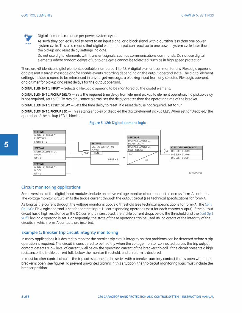
5-238 C70 CAPACITOR BANK PROTECTION AND CONTROL SYSTEM – INSTRUCTION MANUAL
CONTROL ELEMENTS CHAPTER 5: SETTINGS
5
There are 48 identical digital elements available, numbered 1 to 48. A digital element can monitor any FlexLogic operand and present a target message and/or enable events recording depending on the output operand state. The digital element settings include a name to be referenced in any target message, a blocking input from any selected FlexLogic operand, and a timer for pickup and reset delays for the output operand.
DIGITAL ELEMENT 1 INPUT — Selects a FlexLogic operand to be monitored by the digital element.
DIGITAL ELEMENT 1 PICKUP DELAY — Sets the required time delay from element pickup to element operation. If a pickup delay is not required, set to "0," To avoid nuisance alarms, set the delay greater than the operating time of the breaker.
DIGITAL ELEMENT 1 RESET DELAY — Sets the time delay to reset. If a reset delay is not required, set to “0.”
DIGITAL ELEMENT 1 PICKUP LED — This setting enables or disabled the digital element pickup LED. When set to “Disabled,” the operation of the pickup LED is blocked.
Figure 5-126: Digital element logic
Circuit monitoring applicationsSome versions of the digital input modules include an active voltage monitor circuit connected across form-A contacts. The voltage monitor circuit limits the trickle current through the output circuit (see technical specifications for form-A).
As long as the current through the voltage monitor is above a threshold (see technical specifications for form-A), the Cont Op 1 VOn FlexLogic operand is set (for contact input 1—corresponding operands exist for each contact output). If the output circuit has a high resistance or the DC current is interrupted, the trickle current drops below the threshold and the Cont Op 1 VOff FlexLogic operand is set. Consequently, the state of these operands can be used as indicators of the integrity of the circuits in which form-A contacts are inserted.
Example 1: Breaker trip circuit integrity monitoringIn many applications it is desired to monitor the breaker trip circuit integrity so that problems can be detected before a trip operation is required. The circuit is considered to be healthy when the voltage monitor connected across the trip output contact detects a low level of current, well below the operating current of the breaker trip coil. If the circuit presents a high resistance, the trickle current falls below the monitor threshold, and an alarm is declared.
In most breaker control circuits, the trip coil is connected in series with a breaker auxiliary contact that is open when the breaker is open (see figure). To prevent unwanted alarms in this situation, the trip circuit monitoring logic must include the breaker position.
NOTE
Digital elements run once per power system cycle.As such they can easily fail to react to an input signal or a block signal with a duration less than one power system cycle. This also means that digital element output can react up to one power system cycle later than the pickup and reset delay settings indicate.Do not use digital elements with transient signals, such as communications commands. Do not use digital elements where random delays of up to one cycle cannot be tolerated, such as in high speed protection.
SETTINGDIGITAL ELEMENT 01FUNCTION:Enabled = 1
DIGITAL ELEMENT 01BLOCK:Off = 0
FLEXLOGIC OPERANDSDIG ELEM 01 DPODIG ELEM 01 PKP
SETTING
827042A2.VSD
DIGITAL ELEMENT 01INPUT:Off = 0
SETTING
INPUT = 1
RUN tPKP
tRST
DIGITAL ELEMENT 01PICKUP DELAY:
SETTINGS
DIGITAL ELEMENT 01 RESET DELAY:
AND
SETTINGDIGITAL ELEMENT 01 NAME:
DIG ELEM 01 OP

CHAPTER 5: SETTINGS CONTROL ELEMENTS
C70 CAPACITOR BANK PROTECTION AND CONTROL SYSTEM – INSTRUCTION MANUAL 5-239
5
Figure 5-127: Trip circuit example 1
Assume the output contact H1 is a trip contact. Using the contact output settings, this output is given an ID name; for example, “Cont Op 1." Assume a 52a breaker auxiliary contact is connected to contact input H7a to monitor breaker status. Using the contact input settings, this input is given an ID name, for example, “Cont Ip 1," and is set “On” when the breaker is closed. The settings to use digital element 1 to monitor the breaker trip circuit are indicated (EnerVista example shown).
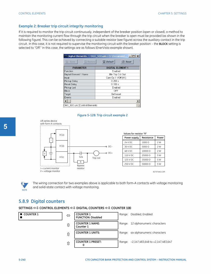
5-240 C70 CAPACITOR BANK PROTECTION AND CONTROL SYSTEM – INSTRUCTION MANUAL
CONTROL ELEMENTS CHAPTER 5: SETTINGS
5
Example 2: Breaker trip circuit integrity monitoringIf it is required to monitor the trip circuit continuously, independent of the breaker position (open or closed), a method to maintain the monitoring current flow through the trip circuit when the breaker is open must be provided (as shown in the following figure). This can be achieved by connecting a suitable resistor (see figure) across the auxiliary contact in the trip circuit. In this case, it is not required to supervise the monitoring circuit with the breaker position – the BLOCK setting is selected to “Off.” In this case, the settings are as follows (EnerVista example shown).
Figure 5-128: Trip circuit example 2
5.8.9 Digital countersSETTINGS CONTROL ELEMENTS DIGITAL COUNTERS COUNTER 1(8)
NOTE
The wiring connection for two examples above is applicable to both form-A contacts with voltage monitoring and solid-state contact with voltage monitoring.
COUNTER 1 COUNTER 1
FUNCTION: DisabledRange: Disabled, Enabled
COUNTER 1 NAME:Counter 1
Range: 12 alphanumeric characters
COUNTER 1 UNITS: Range: six alphanumeric characters
COUNTER 1 PRESET:0
Range: –2,147,483,648 to +2,147,483,647

CHAPTER 5: SETTINGS CONTROL ELEMENTS
C70 CAPACITOR BANK PROTECTION AND CONTROL SYSTEM – INSTRUCTION MANUAL 5-241
5
There are eight identical digital counters, numbered from 1 to 8. A digital counter counts the number of state transitions from Logic 0 to Logic 1. The counter is used to count operations such as the pickups of an element, the changes of state of an external contact (for example, breaker auxiliary switch), or pulses from a watt-hour meter.
COUNTER 1 UNITS — Assigns a label to identify the unit of measure pertaining to the digital transitions to be counted. The units label appears in the corresponding actual values status.
COUNTER 1 PRESET — Sets the count to a required preset value before counting operations begin, as in the case where a substitute relay is to be installed in place of an in-service relay, or while the counter is running.
COUNTER 1 COMPARE — Sets the value to which the accumulated count value is compared. Three FlexLogic output operands are provided to indicate if the present value is ‘more than (HI)’, ‘equal to (EQL)’, or ‘less than (LO)’ the set value.
COUNTER 1 UP — Selects the FlexLogic operand for incrementing the counter. If an enabled UP input is received when the accumulated value is at the limit of +2,147,483,647 counts, the counter rolls over to –2,147,483,648.
COUNTER 1 DOWN — Selects the FlexLogic operand for decrementing the counter. If an enabled DOWN input is received when the accumulated value is at the limit of –2,147,483,648 counts, the counter rolls over to +2,147,483,647.
COUNTER 1 BLOCK — Selects the FlexLogic operand for blocking the counting operation. All counter operands are blocked.
CNT1 SET TO PRESET — Selects the FlexLogic operand used to set the count to the preset value. The counter sets to the preset value in the following situations:
• When the counter is enabled and the CNT1 SET TO PRESET operand has the value 1 (when the counter is enabled and CNT1 SET TO PRESET operand is 0, the counter sets to 0)
• When the counter is running and the CNT1 SET TO PRESET operand changes the state from 0 to 1 (CNT1 SET TO PRESET changing from 1 to 0 while the counter is running has no effect on the count)
• When a reset or reset/freeze command is sent to the counter and the CNT1 SET TO PRESET operand has the value 1 (when a reset or reset/freeze command is sent to the counter and the CNT1 SET TO PRESET operand has the value 0, the counter sets to 0)
COUNTER 1 RESET — Selects the FlexLogic operand for setting the count to either “0” or the preset value depending on the state of the CNT1 SET TO PRESET operand.
COUNTER 1 FREEZE/RESET — Selects the FlexLogic operand for capturing (freezing) the accumulated count value into a separate register with the date and time of the operation, and resetting the count to “0.”
COUNTER 1 FREEZE/COUNT — Selects the FlexLogic operand for capturing (freezing) the accumulated count value into a separate register with the date and time of the operation, and continuing counting. The present accumulated value and captured frozen value with the associated date/time stamp are available as actual values. If control power is interrupted, the accumulated and frozen values are saved into non-volatile memory during the power-down operation.
COUNTER 1 COMPARE:0
Range: –2,147,483,648 to +2,147,483,647
COUNTER 1 UP:Off
Range: FlexLogic operand
COUNTER 1 DOWN:Off
Range: FlexLogic operand
COUNTER 1 BLOCK:Off
Range: FlexLogic operand
CNT1 SET TO PRESET:Off
Range: FlexLogic operand
COUNTER 1 RESET:Off
Range: FlexLogic operand
COUNT1 FREEZE/RESET:Off
Range: FlexLogic operand
COUNT1 FREEZE/COUNT:Off
Range: FlexLogic operand
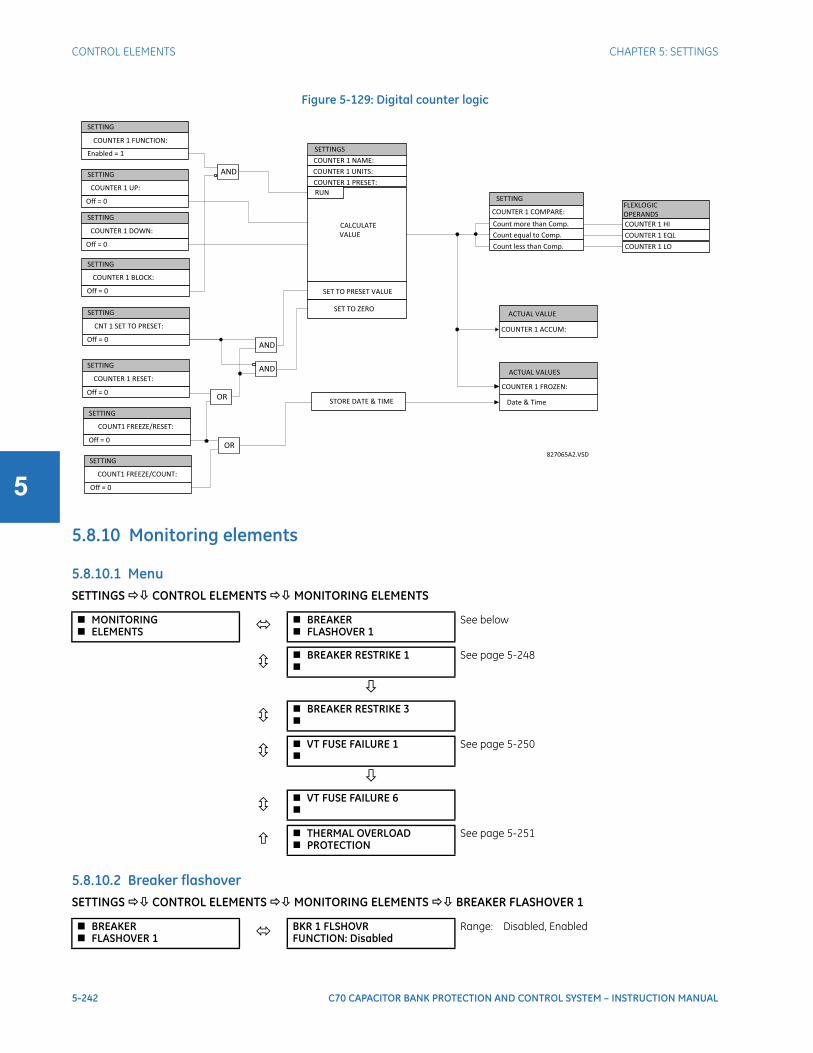
5-242 C70 CAPACITOR BANK PROTECTION AND CONTROL SYSTEM – INSTRUCTION MANUAL
CONTROL ELEMENTS CHAPTER 5: SETTINGS
5
Figure 5-129: Digital counter logic
5.8.10 Monitoring elements
5.8.10.1 MenuSETTINGS CONTROL ELEMENTS MONITORING ELEMENTS
5.8.10.2 Breaker flashoverSETTINGS CONTROL ELEMENTS MONITORING ELEMENTS BREAKER FLASHOVER 1
MONITORING ELEMENTS BREAKER
FLASHOVER 1See below
BREAKER RESTRIKE 1
See page 5-248
BREAKER RESTRIKE 3
VT FUSE FAILURE 1
See page 5-250
VT FUSE FAILURE 6
THERMAL OVERLOAD PROTECTION
See page 5-251
BREAKER FLASHOVER 1 BKR 1 FLSHOVR
FUNCTION: DisabledRange: Disabled, Enabled
827065A2.VSD
FLEXLOGIC OPERANDSCOUNTER 1 HICOUNTER 1 EQLCOUNTER 1 LO
SETTING
COUNTER 1 FUNCTION:
Enabled = 1
COUNTER 1 BLOCK:
COUNTER 1 UP:
COUNTER 1 DOWN:
COUNTER 1 RESET:
COUNT1 FREEZE/RESET:
COUNT1 FREEZE/COUNT:
Off = 0
COUNTER 1 UNITS:COUNTER 1 PRESET:
CALCULATEVALUE
RUN
SET TO PRESET VALUE
STORE DATE & TIME
COUNTER 1 NAME:
COUNTER 1 COMPARE: Count more than Comp.Count equal to Comp.Count less than Comp.
COUNTER 1 FROZEN:
Date & Time
CNT 1 SET TO PRESET:
SET TO ZERO
SETTING
SETTING
SETTING
SETTING
SETTING
SETTING
SETTING
SETTINGS
Off = 0
Off = 0
Off = 0
Off = 0
Off = 0
Off = 0
ACTUAL VALUES
COUNTER 1 ACCUM:
ACTUAL VALUE
SETTING
AND
OR
OR
AND
AND
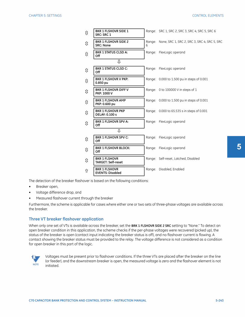
CHAPTER 5: SETTINGS CONTROL ELEMENTS
C70 CAPACITOR BANK PROTECTION AND CONTROL SYSTEM – INSTRUCTION MANUAL 5-243
5
The detection of the breaker flashover is based on the following conditions:
• Breaker open,
• Voltage difference drop, and
• Measured flashover current through the breaker
Furthermore, the scheme is applicable for cases where either one or two sets of three-phase voltages are available across the breaker.
Three VT breaker flashover applicationWhen only one set of VTs is available across the breaker, set the BRK 1 FLSHOVR SIDE 2 SRC setting to “None.” To detect an open breaker condition in this application, the scheme checks if the per-phase voltages were recovered (picked up), the status of the breaker is open (contact input indicating the breaker status is off), and no flashover current is flowing. A contact showing the breaker status must be provided to the relay. The voltage difference is not considered as a condition for open breaker in this part of the logic.
BKR 1 FLSHOVR SIDE 1SRC: SRC 1
Range: SRC 1, SRC 2, SRC 3, SRC 4, SRC 5, SRC 6
BKR 1 FLSHOVR SIDE 2SRC: None
Range: None, SRC 1, SRC 2, SRC 3, SRC 4, SRC 5, SRC 6
BKR 1 STATUS CLSD A:Off
Range: FlexLogic operand
BKR 1 STATUS CLSD C:Off
Range: FlexLogic operand
BKR 1 FLSHOVR V PKP:0.850 pu
Range: 0.000 to 1.500 pu in steps of 0.001
BKR 1 FLSHOVR DIFF VPKP: 1000 V
Range: 0 to 100000 V in steps of 1
BKR 1 FLSHOVR AMPPKP: 0.600 pu
Range: 0.000 to 1.500 pu in steps of 0.001
BKR 1 FLSHOVR PKPDELAY: 0.100 s
Range: 0.000 to 65.535 s in steps of 0.001
BKR 1 FLSHOVR SPV A:Off
Range: FlexLogic operand
BKR 1 FLSHOVR SPV C:Off
Range: FlexLogic operand
BKR 1 FLSHOVR BLOCK:Off
Range: FlexLogic operand
BKR 1 FLSHOVRTARGET: Self-reset
Range: Self-reset, Latched, Disabled
BKR 1 FLSHOVREVENTS: Disabled
Range: Disabled, Enabled
NOTE
Voltages must be present prior to flashover conditions. If the three VTs are placed after the breaker on the line (or feeder), and the downstream breaker is open, the measured voltage is zero and the flashover element is not initiated.

5-244 C70 CAPACITOR BANK PROTECTION AND CONTROL SYSTEM – INSTRUCTION MANUAL
CONTROL ELEMENTS CHAPTER 5: SETTINGS
5
The flashover detection resets if the current drops back to zero, the breaker closes, or the selected FlexLogic operand for supervision changes to high. Using supervision through the BRK 1 FLSHOVR SPV A, BRK 1 FLSHOVR SPV B, and BRK 1 FLSHOVR SPV c settings is recommended by selecting a trip operand that does not allow the flashover element to pickup prior to the trip.
The flashover detection can be used for external alarm, re-tripping the breaker, or energizing the lockout relay.
Consider the following configuration:
The source 1 (SRC1) phase currents are feeder CTs and phase voltages are bus VTs, and Contact Input 1 is set as Breaker 52a contact. The conditions prior to flashover detection are:
• 52a status = 0
• VAg, VBg, or VCg is greater than the pickup setting
• IA, IB, IC = 0; no current flows through the breaker
• ΔVA is greater than pickup (not applicable in this scheme)
The conditions at flashover detection are:
• 52a status = 0
• IA, IB, or IC is greater than the pickup current flowing through the breaker
• ΔVA is greater than pickup (not applicable in this scheme)
Six VT breaker flashover applicationThe per-phase voltage difference approaches zero when the breaker is closed. This is well below any typical minimum pickup voltage. Select the level of the BRK 1 FLSHOVR DIFF V PKP setting to be less than the voltage difference measured across the breaker when the close or open breaker resistors are left in service. Prior to flashover, the voltage difference is larger than BRK 1 FLSHOVR DIFF V PKP. This applies to either the difference between two live voltages per phase or when the voltage from one side of the breaker has dropped to zero (line de-energized), at least one per-phase voltage is larger than the BRK 1 FLSHOVR V PKP setting, and no current flows through the breaker poles. During breaker flashover, the per-phase voltages from both sides of the breaker drops below the pickup value defined by the BRK 1 FLSHOVR V PKP setting, the voltage difference drops below the pickup setting, and flashover current is detected. These flashover conditions initiate FlexLogic pickup operands and start the BRK 1 FLSHOVR PKP DELAY timer.
This application does not require detection of breaker status via a 52a contact, as it uses a voltage difference larger than the BRK 1 FLSHOVR DIFF V PKP setting. However, monitoring the breaker contact ensures scheme stability.

CHAPTER 5: SETTINGS CONTROL ELEMENTS
C70 CAPACITOR BANK PROTECTION AND CONTROL SYSTEM – INSTRUCTION MANUAL 5-245
5
Consider the following configuration:
The source 1 (SRC1) phase currents are CTs and phase voltages are bus VTs. The source 2 (SRC2) phase voltages are line VTs. Contact input 1 is set as the breaker 52a contact (optional).
The conditions prior to flashover detection are:
• ΔVA is greater than pickup
• IA, IB, IC = 0; no current flows through the breaker
• 52a status = 0 (optional)
The conditions at flashover detection are:
• ΔVA is less than pickup
• VAg, VBg, or VCg is lower than the pickup setting
• IA, IB, or IC is greater than the pickup current flowing through the breaker
• 52a status = 0 (optional)
SettingsBRK 1 FLSHOVR SIDE 1 SRC — This setting specifies a signal source used to provide three-phase voltages and three-phase currents from one side of the current breaker. The source selected as a setting and must be configured with breaker phase voltages and currents, even if only three VTs are available across the breaker.
BRK 1 FLSHOVR SIDE 2 SRC — This setting specifies a signal source used to provide another set of three phase voltages whenever six VTs are available across the breaker.
BRK 1 STATUS CLSD A to BRK 1 STATUS CLSD C — These settings specify FlexLogic operands to indicate the open status of the breaker. A separate FlexLogic operand can be selected to detect individual breaker pole status and provide flashover detection. The recommended setting is 52a breaker contact or another operand defining the breaker poles open status.
BRK 1 FLSHOVR V PKP — This setting specifies a pickup level for the phase voltages from both sides of the breaker. If six VTs are available, opening the breaker leads to two possible combinations – live voltages from only one side of the breaker, or live voltages from both sides of the breaker. Either case sets the scheme for flashover detection upon detection of voltage above the selected value. Set BRK FLSHOVR V PKP to 85 to 90% of the nominal voltage.
BRK 1 FLSHOVR DIFF V PKP — This setting specifies a pickup level for the phase voltage difference when two VTs per phase are available across the breaker. The pickup voltage difference should be below the monitored voltage difference when close or open breaker resistors are left in service. The setting is selected as primary volts difference between the sources.
BRK 1 FLSHOVR AMP PKP — This setting specifies the normal load current which can flow through the breaker. Depending on the flashover protection application, the flashover current can vary from levels of the charging current when the line is de-energized (all line breakers open), to well above the maximum line (feeder) load (line/feeder connected to load).
NOTE
The element operates only when phase-to-ground voltages are connected to relay terminals. The flashover element does not operate if delta voltages are applied.

5-246 C70 CAPACITOR BANK PROTECTION AND CONTROL SYSTEM – INSTRUCTION MANUAL
CONTROL ELEMENTS CHAPTER 5: SETTINGS
5
BRK 1 FLSHOVR SPV A to BRK 1 FLSHOVR SPV C — These settings specify FlexLogic operands (per breaker pole) that supervise the operation of the element per phase. Supervision can be provided by operation of other protection elements, breaker failure, and close and trip commands. A six-cycle time delay applies after the selected FlexLogic operand resets.
BRK FLSHOVR PKP DELAY — This setting specifies the time delay to operate after a pickup condition is detected.
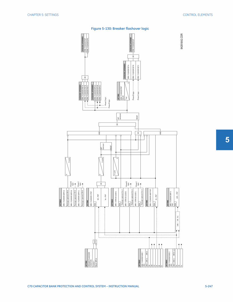
CHAPTER 5: SETTINGS CONTROL ELEMENTS
C70 CAPACITOR BANK PROTECTION AND CONTROL SYSTEM – INSTRUCTION MANUAL 5-247
5
Figure 5-130: Breaker flashover logic

5-248 C70 CAPACITOR BANK PROTECTION AND CONTROL SYSTEM – INSTRUCTION MANUAL
CONTROL ELEMENTS CHAPTER 5: SETTINGS
5
5.8.10.3 Breaker restrikeSETTINGS CONTROL ELEMENTS MONITORING ELEMENTS BREAKER RESTRIKE 1(3)
One breaker restrike element is provided for each CT/VT module in the C70.
According to IEEE standard C37.100 entitled IEEE Standard Definitions for Power Switchgear, restrike is defined as “a resumption of current between the contacts of a switching device during an opening operation after an interval of zero current of ¼ cycle at normal frequency or longer.”
Figure 5-131: Typical restrike waveform and detection flag
The breaker restrike algorithm responds to a successful interruption of the phase current following a declaration of capacitor bank offline as per the breaker pole indication. If a high-frequency current with a magnitude greater than the threshold is resumed at least ¼ of a cycle later than the phase current interruption, then a breaker restrike condition is declared in the corresponding phase and the BRK RESTRIKE 1 OP operand asserts for a short period of time. The user can add counters and other logic to facilitate the decision making process as to the appropriate actions upon detecting a single restrike or a series of consecutive restrikes.
A restrike event (FlexLogic operand) is declared if all of the following hold:
• The current is initially interrupted
BREAKER RESTRIKE 1 BREAKER RESTRIKE 1
FUNCTION: DisabledRange: Disabled, Enabled
BKR RSTR 1 BLOCK:Off
Range: FlexLogic operand
BREAKER RESTRIKE 1SOURCE: SRC 1
Range: SRC 1, SRC 2, SRC 3, SRC 4, SRC 5, SRC 6
BREAKER RESTRIKE 1PICKUP: 0.500 pu
Range: 0.10 to 2.00 pu in steps of 0.01
BREAKER RESTRIKE 1RESET DELAY: 0.100 s
Range: 0.000 to 65.535 s in steps of 0.001
BKR RSTR 1 BKR OPEN:Off
Range: FlexLogic operand
BKR RSTR 1 OPEN CMD:Off
Range: FlexLogic operand
BKR RSTR 1 CLS CMD:Off
Range: FlexLogic operand
BREAKER RESTRIKE 1TARGET: Self-reset
Range: Self-reset, Latched, Disabled
BREAKER RESTRIKE 1EVENTS: Disabled
Range: Disabled, Enabled
0
2
4
6
8
10
–2
–4
–6
–8
–10
0.01
0.02
0.03
0.05
time (ms)
cu
rre
nt
(am
ps)
OPERATE
834764A1.CDR

CHAPTER 5: SETTINGS CONTROL ELEMENTS
C70 CAPACITOR BANK PROTECTION AND CONTROL SYSTEM – INSTRUCTION MANUAL 5-249
5
• The breaker status is open
• An elevated high frequency current condition occurs and the current subsequently drops out again
The algorithm is illustrated in the following state machine diagram.
Figure 5-132: Algorithm illustration of state machine to detect restrike
In this way, a distinction is made between a self-extinguishing restrike and permanent breaker failure condition. The latter can be detected by the breaker failure function or a regular instantaneous overcurrent element. Also, a fast succession of restrikes is picked up by breaker failure or instantaneous overcurrent protection.
The following settings are available for each element.
BREAKER RESTRIKE 1 FUNCTION — Enables and disables operation of the breaker restrike detection element.
BRK RSTR 1 BLOCK — Blocks operation of the breaker restrike detection element.
BREAKER RESTRIKE 1 SOURCE — Selects the source of the current for this element. This source must have a valid CT bank assigned.
BREAKER RESTRIKE 1 PICKUP — Specifies the pickup level of the overcurrent detector in per-unit values of CT nominal current.
BREAKER RESTRIKE 1 RESET DELAY — Specifies the reset delay for this element. When set to “0 ms,” then FlexLogic operand is picked up for only 1/8th of the power cycle.
BRK RSTR 1 BRK OPEN — Assigns a FlexLogic operand indicating the open position of the breaker. It must be logic “1” when the breaker is open.
BRK RSTR 1 OPEN CMD — Assigns a FlexLogic operand indicating a breaker open command. It must be logic “1” when the breaker is opened, either manually or from protection logic.
BRK RSTR 1 CLS CMD — Assigns a FlexLogic operand indicating a breaker close command. It must be logic “1” when the breaker is closed.
Capacitor bank
offline
Current
interruption
(overcurrent)
High-frequency
elevated current
Restrike detected:
OP state asserted
Breaker close
Breaker
close
Breaker
close
Capacitor bank
online
Current
interruption
(overcurrent)
Breaker open
command or breaker
open state
834768A1.CDR
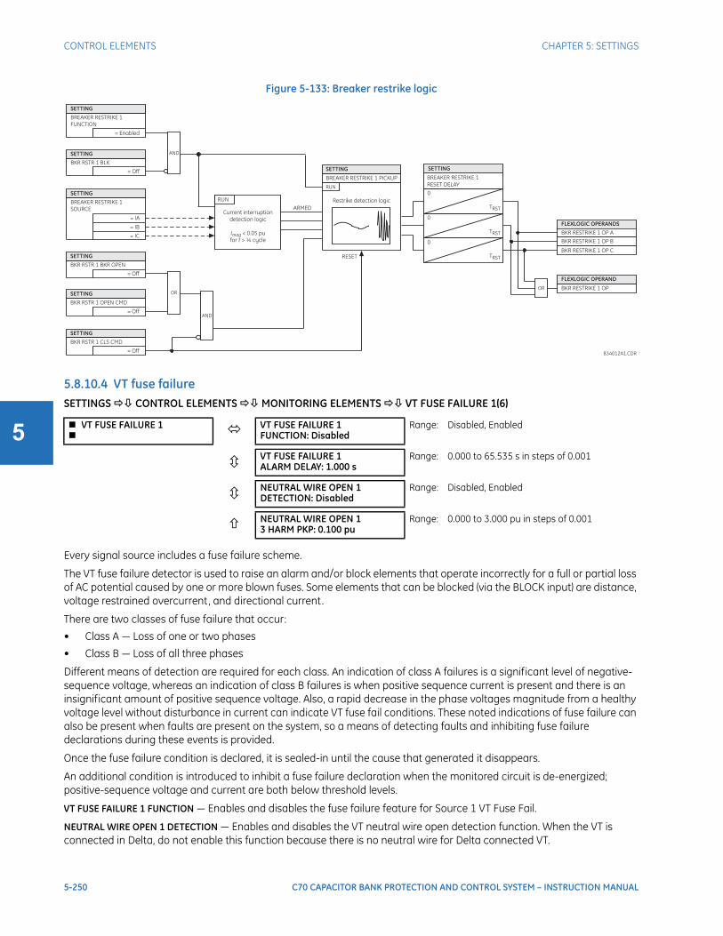
5-250 C70 CAPACITOR BANK PROTECTION AND CONTROL SYSTEM – INSTRUCTION MANUAL
CONTROL ELEMENTS CHAPTER 5: SETTINGS
5
Figure 5-133: Breaker restrike logic
5.8.10.4 VT fuse failureSETTINGS CONTROL ELEMENTS MONITORING ELEMENTS VT FUSE FAILURE 1(6)
Every signal source includes a fuse failure scheme.
The VT fuse failure detector is used to raise an alarm and/or block elements that operate incorrectly for a full or partial loss of AC potential caused by one or more blown fuses. Some elements that can be blocked (via the BLOCK input) are distance, voltage restrained overcurrent, and directional current.
There are two classes of fuse failure that occur:
• Class A — Loss of one or two phases
• Class B — Loss of all three phases
Different means of detection are required for each class. An indication of class A failures is a significant level of negative-sequence voltage, whereas an indication of class B failures is when positive sequence current is present and there is an insignificant amount of positive sequence voltage. Also, a rapid decrease in the phase voltages magnitude from a healthy voltage level without disturbance in current can indicate VT fuse fail conditions. These noted indications of fuse failure can also be present when faults are present on the system, so a means of detecting faults and inhibiting fuse failure declarations during these events is provided.
Once the fuse failure condition is declared, it is sealed-in until the cause that generated it disappears.
An additional condition is introduced to inhibit a fuse failure declaration when the monitored circuit is de-energized; positive-sequence voltage and current are both below threshold levels.
VT FUSE FAILURE 1 FUNCTION — Enables and disables the fuse failure feature for Source 1 VT Fuse Fail.
NEUTRAL WIRE OPEN 1 DETECTION — Enables and disables the VT neutral wire open detection function. When the VT is connected in Delta, do not enable this function because there is no neutral wire for Delta connected VT.
VT FUSE FAILURE 1 VT FUSE FAILURE 1
FUNCTION: DisabledRange: Disabled, Enabled
VT FUSE FAILURE 1ALARM DELAY: 1.000 s
Range: 0.000 to 65.535 s in steps of 0.001
NEUTRAL WIRE OPEN 1DETECTION: Disabled
Range: Disabled, Enabled
NEUTRAL WIRE OPEN 13 HARM PKP: 0.100 pu
Range: 0.000 to 3.000 pu in steps of 0.001
RUN
Current interruption
detection logic
< 0.05 pu
for > ¼ cycle
I
tmag
ARMED
RESET
SETTING
= Enabled
BREAKER RESTRIKE 1
FUNCTION
SETTING
= Off
BKR RSTR 1 BLK
AND
SETTING
= IA
BREAKER RESTRIKE 1
SOURCE
= IB
= IC
SETTING
= Off
BKR RSTR 1 BKR OPEN
SETTING
= Off
BKR RSTR 1 OPEN CMD
SETTING
= Off
BKR RSTR 1 CLS CMD
AND
OR
SETTING
BREAKER RESTRIKE 1 PICKUP
RUN
Restrike detection logic
0
TRST
SETTING
BREAKER RESTRIKE 1
RESET DELAY
0
TRST
0
TRST
FLEXLOGIC OPERANDS
BKR RESTRIKE 1 OP A
BKR RESTRIKE 1 OP B
BKR RESTRIKE 1 OP C
BKR RESTRIKE 1 OP
FLEXLOGIC OPERAND
OR
834012A1.CDR

CHAPTER 5: SETTINGS CONTROL ELEMENTS
C70 CAPACITOR BANK PROTECTION AND CONTROL SYSTEM – INSTRUCTION MANUAL 5-251
5
NEUTRAL WIRE OPEN 1 3 HRAM PKP — Specifies the pickup level of 3rd harmonic of 3V0 signal for the NEUTRAL WIRE OPEN DETECTION logic to pick up.
Base voltage for this element is PHASE VT SECONDARY setting in the case of WYE VTs and (PHASE VT SECONDARY)/ in case of DELTA VTs. The setting is found under SETTINGS SYSTEM SETUP AC INPUTS VOLTAGE BANK PHASE VT SECONDARY.
Figure 5-134: VT fuse fail logic
5.8.10.5 Thermal overload protection (ANSI 49)SETTINGS CONTROL ELEMENTS MONITORING ELEMENTS THERMAL OVERLOAD PROTECTION THERMAL PROTECTION 1(2)
THERMAL PROTECTION 1 THERMAL PROTECTION 1
FUNCTION: DisabledRange: Disabled, Enabled
THERMAL PROTECTION 1SOURCE: SRC1
Range: SRC 1, SRC 2, SRC 3, SRC 4, SRC 5, SRC 6
THERMAL PROTECTION 1BASE CURR: 0.80 pu
Range: 0.20 to 3.00 pu in steps of 0.01
THERMAL PROTECTION 1k FACTOR: 1.10
Range: 1.00 to 1.20 in steps of 0.05
3
827093AQ.CDR
FUSE FAIL
FAULT
AND
AND
AND
SET
RESET
Reset-dominant
Latch
AND
AND
AND
AND
OR
OR
OR
OR
FunctionSETTING
Enabled = 1
SOURCE 1
V_2
V_1
I_1
RunV_1 < 0.05 pu
RunV_2 > 0.1 pu
RunI_1 > 0.075 pu
RunV_1 < 0.80 pu
RunI_1 < 0.05 pu
SRC1 50DD OPFLEXLOGIC OPERANDS
2 cycles
20 cyclesSRC1 VT FUSE FAIL OPFLEXLOGIC OPERANDS
SRC1 VT FUSE FAIL DPO
SRC1 VT FUSE FAIL VOL LOSS
FLEXLOGIC OPERAND
TIMER
OPEN POLE OP
The OPEN POLE OP operand appliesto the D60, L60, and L90
Neutral Wire Open DetectSETTING
Enabled = 1
SOURCE 13V_0 (3rd Harmonic)
SETTING
Run3V_0 3rd Harm >setting
3 HARM PKP
AND
SRC1 3V0 3nd Harmonic
FLEX-ANALOG
AND 5 cycles
0
TIMER
SRC1 VT NEU WIRE OPEN
FLEXLOGIC OPERANDOR
AND
0
20 cycles
TIMER
2 cycles
0
TIMER
30 cycles
0
TIMER
COMPARATORS
VA
VB
VC
Run|VB|-|VB| > 0.2 pu
& |VB| > 0.8 pu
Run|VA|-|VA| > 0.2 pu
& |VA| > 0.8 pu
Run|VC|-|VC| > 0.2 pu
& |VC| > 0.8 pu
OR
VA, VB and VC are the voltage magnitude of one cycle before

5-252 C70 CAPACITOR BANK PROTECTION AND CONTROL SYSTEM – INSTRUCTION MANUAL
CONTROL ELEMENTS CHAPTER 5: SETTINGS
5
The thermal overload protection element corresponds to the IEC 255-8 standard and is used to detect thermal overload conditions in protected power system elements. Choosing an appropriate time constant element can be used to protect different elements of the power system. The cold curve characteristic is applied when the previous averaged load current over the last 5 cycles is less than 10% of the base current. If this current is greater or equal than 10% than the base current, then the hot curve characteristic is applied.
The IEC255-8 cold curve is defined as follows:
Eq. 5-21
The IEC255-8 hot curve is defined as follows:
Eq. 5-22
where
top = time to operateτop = thermal protection trip time constantI = measured overload RMS currentIp = measured load RMS current before overload occursk = IEC 255-8 k-factor applied to IB, defining maximum permissible current above nominal currentIB = protected element base (nominal) current
To ensure element accuracy for high overcurrent conditions, the maximum value of I/(k x IB) is limited to 8, even when realistically it is exceeding this value.
The reset time of the thermal overload protection element is also time delayed using following formula:
Eq. 5-23
where
τrst = thermal protection trip time constantTmin = a minimum reset time setting
THERM PROT 1 TRIPTIME CONST: 45 min.
Range: 0 to 1000 min. in steps of 1
THERM PROT 1 RESETTIME CONST: 45 min.
Range: 0 to 1000 min. in steps of 1
THERM PROT 1 MINIMRESET TIME: 20 min.
Range: 0 to 1000 min. in steps of 1
THERM PROT 1 RESET:Off
Range: FlexLogic operand
THERM PROT 1 BLOCK:Off
Range: FlexLogic operand
THERMAL PROTECTION 1TARGET: Self-reset
Range: Self-reset, Latched, Disabled
THERMAL PROTECTION 1EVENTS: Disabled
Range: Disabled, Enabled
top τopI2
I2 kIB( )2–
-----------------------
ln×=
top τop
I2 Ip2
–
I2 kIB( )2–
-----------------------
ln×=
trst τrst
kIB( )2
I2 kIB( )2–
-------------------------
ln× Tmin+=

CHAPTER 5: SETTINGS CONTROL ELEMENTS
C70 CAPACITOR BANK PROTECTION AND CONTROL SYSTEM – INSTRUCTION MANUAL 5-253
5
Figure 5-135: IEC 255-8 sample operate and reset curves
The thermal overload protection element estimates accumulated thermal energy E using the following equations calculated each power cycle. When current is greater than the pickup level, In > k × IB, element starts increasing the thermal energy:
Eq. 5-24
When current is less than the dropout level, In > 0.97 × k × IB, the element starts decreasing the thermal energy:
Eq. 5-25
where
∆t is the power cycle durationn is the power cycle indextop(In) is the trip time calculated at index n as per the IEC255-8 cold curve or hot curve equationstrst(In) is the reset time calculated at index n as per the reset time equation
En En 1–tΔ
top In( )--------------+=
En En 1–tΔ
trst In( )--------------–=

5-254 C70 CAPACITOR BANK PROTECTION AND CONTROL SYSTEM – INSTRUCTION MANUAL
INPUTS/OUTPUTS CHAPTER 5: SETTINGS
5
In is the measured overload RMS current at index nEn is the accumulated energy at index nEn – 1 is the accumulated energy at index n – 1
The thermal overload protection element removes the THERMAL PROT 1 OP output operand when E < 0.05. In case of emergency, the thermal memory and THERMAL PROT 1 OP output operand can be reset using THERM PROT 1 RESET setting. All calculations are performed per phase. If the accumulated energy reaches value 1 in any phase, the thermal overload protection element operates and only resets when energy is less than 0.05 in all three phases.
Table 5-35: Typical time constants
The figure shows the logic for the thermal overload protection element.
Figure 5-136: Thermal overload protection logic
5.9 Inputs/outputs
5.9.1 Contact inputsSETTINGS INPUTS/OUTPUTS CONTACT INPUTS
Protected equipment Time constant Minimum reset time
Capacitor bank 10 minutes 30 minutes
Overhead line 10 minutes 20 minutes
Air-core reactor 40 minutes 30 minutes
Busbar 60 minutes 20 minutes
Underground cable 20 to 60 minutes 60 minutes
CONTACT INPUTS
CONTACT INPUT H5a
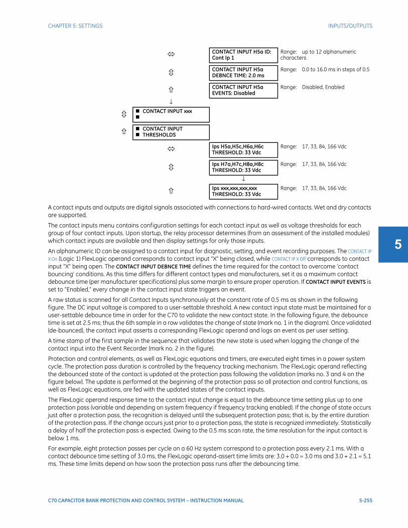
CHAPTER 5: SETTINGS INPUTS/OUTPUTS
C70 CAPACITOR BANK PROTECTION AND CONTROL SYSTEM – INSTRUCTION MANUAL 5-255
5
A contact inputs and outputs are digital signals associated with connections to hard-wired contacts. Wet and dry contacts are supported.
The contact inputs menu contains configuration settings for each contact input as well as voltage thresholds for each group of four contact inputs. Upon startup, the relay processor determines (from an assessment of the installed modules) which contact inputs are available and then display settings for only those inputs.
An alphanumeric ID can be assigned to a contact input for diagnostic, setting, and event recording purposes. The CONTACT IP X On (Logic 1) FlexLogic operand corresponds to contact input “X” being closed, while CONTACT IP X Off corresponds to contact input “X” being open. The CONTACT INPUT DEBNCE TIME defines the time required for the contact to overcome ‘contact bouncing’ conditions. As this time differs for different contact types and manufacturers, set it as a maximum contact debounce time (per manufacturer specifications) plus some margin to ensure proper operation. If CONTACT INPUT EVENTS is set to “Enabled,” every change in the contact input state triggers an event.
A raw status is scanned for all Contact Inputs synchronously at the constant rate of 0.5 ms as shown in the following figure. The DC input voltage is compared to a user-settable threshold. A new contact input state must be maintained for a user-settable debounce time in order for the C70 to validate the new contact state. In the following figure, the debounce time is set at 2.5 ms; thus the 6th sample in a row validates the change of state (mark no. 1 in the diagram). Once validated (de-bounced), the contact input asserts a corresponding FlexLogic operand and logs an event as per user setting.
A time stamp of the first sample in the sequence that validates the new state is used when logging the change of the contact input into the Event Recorder (mark no. 2 in the figure).
Protection and control elements, as well as FlexLogic equations and timers, are executed eight times in a power system cycle. The protection pass duration is controlled by the frequency tracking mechanism. The FlexLogic operand reflecting the debounced state of the contact is updated at the protection pass following the validation (marks no. 3 and 4 on the figure below). The update is performed at the beginning of the protection pass so all protection and control functions, as well as FlexLogic equations, are fed with the updated states of the contact inputs.
The FlexLogic operand response time to the contact input change is equal to the debounce time setting plus up to one protection pass (variable and depending on system frequency if frequency tracking enabled). If the change of state occurs just after a protection pass, the recognition is delayed until the subsequent protection pass; that is, by the entire duration of the protection pass. If the change occurs just prior to a protection pass, the state is recognized immediately. Statistically a delay of half the protection pass is expected. Owing to the 0.5 ms scan rate, the time resolution for the input contact is below 1 ms.
For example, eight protection passes per cycle on a 60 Hz system correspond to a protection pass every 2.1 ms. With a contact debounce time setting of 3.0 ms, the FlexLogic operand-assert time limits are: 3.0 + 0.0 = 3.0 ms and 3.0 + 2.1 = 5.1 ms. These time limits depend on how soon the protection pass runs after the debouncing time.
CONTACT INPUT H5a ID:Cont Ip 1
Range: up to 12 alphanumeric characters
CONTACT INPUT H5aDEBNCE TIME: 2.0 ms
Range: 0.0 to 16.0 ms in steps of 0.5
CONTACT INPUT H5aEVENTS: Disabled
Range: Disabled, Enabled
↓
CONTACT INPUT xxx
CONTACT INPUT THRESHOLDS
Ips H5a,H5c,H6a,H6cTHRESHOLD: 33 Vdc
Range: 17, 33, 84, 166 Vdc
Ips H7a,H7c,H8a,H8cTHRESHOLD: 33 Vdc
Range: 17, 33, 84, 166 Vdc
↓
Ips xxx,xxx,xxx,xxxTHRESHOLD: 33 Vdc
Range: 17, 33, 84, 166 Vdc

5-256 C70 CAPACITOR BANK PROTECTION AND CONTROL SYSTEM – INSTRUCTION MANUAL
INPUTS/OUTPUTS CHAPTER 5: SETTINGS
5
Regardless of the contact debounce time setting, the contact input event is time-stamped with a 1 μs accuracy using the time of the first scan corresponding to the new state (mark no. 2 shown). Therefore, the time stamp reflects a change in the DC voltage across the contact input terminals that was not accidental as it was subsequently validated using the debounce timer. Keep in mind that the associated FlexLogic operand is asserted/de-asserted later, after validating the change.
The debounce algorithm is symmetrical: the same procedure and debounce time are used to filter the LOW-HIGH (marks no.1, 2, 3, and 4 in the figure) and HIGH-LOW (marks no. 5, 6, 7, and 8) transitions.
Figure 5-137: Input contact debouncing mechanism and time-stamping sample timing
Contact inputs are isolated in groups of four to allow connection of wet contacts from different voltage sources for each group. The CONTACT INPUT THRESHOLDS determine the minimum voltage required to detect a closed contact input. This value is selected according to the following criteria: 17 for 24 V sources, 33 for 48 V sources, 84 for 110 to 125 V sources and 166 for 250 V sources.
For example, to use contact input H5a as a status input from the breaker 52b contact to seal-in the trip relay and record it in the Event Records menu, make the following settings changes:
CONTACT INPUT H5a ID: "Breaker Closed (52b)"CONTACT INPUT H5a EVENTS: "Enabled"
Note that the 52b contact is closed when the breaker is open and open when the breaker is closed.
5.9.2 Virtual inputsSETTINGS INPUTS/OUTPUTS VIRTUAL INPUTS VIRTUAL INPUT 1(64)
VIRTUAL INPUT 1 VIRTUAL INPUT 1
FUNCTION: DisabledRange: Disabled, Enabled
VIRTUAL INPUT 1 ID:Virt Ip 1
Range: up to 12 alphanumeric characters
VIRTUAL INPUT 1TYPE: Latched
Range: Self-Reset, Latched
842709A1.cdr
DEBOUNCE TIME
(user setting)
At this time, the
new (HIGH)
contact state is
validated
The FlexLogicTM
operand is going to
be asserted at this
protection pass
The FlexLogicTM operand
changes reflecting the
validated contact state
Time stamp of the first
scan corresponding to
the new validated state is
logged in the SOE record
2 1 3
4
DEBOUNCE TIME
(user setting)
At this time, the new
(LOW) contact state is
validated
The FlexLogicTM
operand is going to be
de-asserted at this
protection pass
The FlexLogicTM operand
changes reflecting the
validated contact state
5
7
8
Time stamp of the first
scan corresponding to the
new validated state is
logged in the SOE record
6
SCAN TIME
(0.5 msec)
PROTECTION PASS
(8 times a cycle controlled by the
frequency tracking mechanism)
RA
WC
ON
TA
CT
ST
AT
E
FLE
XLO
GIC
TM
OP
ER
AN
D
INP
UT
VO
LT
AG
E
USER-PROGRAMMABLE THRESHOLD

CHAPTER 5: SETTINGS INPUTS/OUTPUTS
C70 CAPACITOR BANK PROTECTION AND CONTROL SYSTEM – INSTRUCTION MANUAL 5-257
5
The virtual inputs and outputs are digital signals associated with UR-series internal logic signals. Virtual inputs include signals generated by the local user interface. The virtual outputs are outputs of FlexLogic™ equations used to customize the device. Virtual outputs can also serve as virtual inputs to FlexLogic equations.
There are 64 virtual inputs that can be individually programmed to respond to input signals from the keypad (via the COMMANDS menu) and communications protocols. All virtual input operands are defaulted to “Off” (logic 0) unless the appropriate input signal is received.
If the VIRTUAL INPUT x FUNCTION is to “Disabled,” the input is forced to off (logic 0) regardless of any attempt to alter the input. If set to “Enabled,” the input operates as shown on the logic diagram and generates output FlexLogic operands in response to received input signals and the applied settings.
There are two types of operation: self-reset and latched. If VIRTUAL INPUT x type is “Self-Reset,” when the input signal transits from off to on, the output operand is set to on for only one evaluation of the FlexLogic equations and then return to off. If set to “Latched,” the virtual input sets the state of the output operand to the same state as the most recent received input.
The self-reset operating mode generates the output operand for a single evaluation of the FlexLogic equations. If the operand is to be used anywhere other than internally in a FlexLogic equation, it likely needs to be lengthened in time. A FlexLogic timer with a delayed reset can perform this function.
Figure 5-138: Virtual inputs logic
5.9.3 Contact outputs
5.9.3.1 Digital outputsSETTINGS INPUTS/OUTPUTS CONTACT OUTPUTS CONTACT OUTPUT H1
A contact inputs and outputs are digital signals associated with connections to hard-wired contacts. Wet and dry contacts are supported.
Upon startup of the relay, the main processor determines from an assessment of the modules installed in the chassis which contact outputs are available and then present the settings for only these outputs.
VIRTUAL INPUT 1EVENTS: Disabled
Range: Disabled, Enabled
CONTACT OUTPUT H1 CONTACT OUTPUT H1 ID
Cont Op 1Range: up to 12 alphanumeric characters
OUTPUT H1 OPERATE:Off
Range: FlexLogic operand
OUTPUT H1 SEAL-IN:Off
Range: FlexLogic operand
CONTACT OUTPUT H1EVENTS: Enabled
Range: Disabled, Enabled
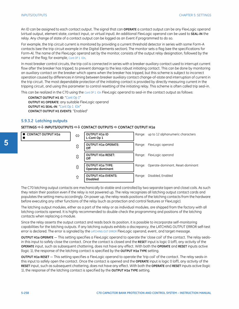
5-258 C70 CAPACITOR BANK PROTECTION AND CONTROL SYSTEM – INSTRUCTION MANUAL
INPUTS/OUTPUTS CHAPTER 5: SETTINGS
5
An ID can be assigned to each contact output. The signal that can OPERATE a contact output can be any FlexLogic operand (virtual output, element state, contact input, or virtual input). An additional FlexLogic operand can be used to SEAL-IN the relay. Any change of state of a contact output can be logged as an Event if programmed to do so.
For example, the trip circuit current is monitored by providing a current threshold detector in series with some Form-A contacts (see the trip circuit example in the Digital Elements section). The monitor sets a flag (see the specifications for Form-A). The name of the FlexLogic operand set by the monitor, consists of the output relay designation, followed by the name of the flag; for example, Cont OP 1 IOn.
In most breaker control circuits, the trip coil is connected in series with a breaker auxiliary contact used to interrupt current flow after the breaker has tripped, to prevent damage to the less robust initiating contact. This can be done by monitoring an auxiliary contact on the breaker which opens when the breaker has tripped, but this scheme is subject to incorrect operation caused by differences in timing between breaker auxiliary contact change-of-state and interruption of current in the trip circuit. The most dependable protection of the initiating contact is provided by directly measuring current in the tripping circuit, and using this parameter to control resetting of the initiating relay. This scheme is often called trip seal-in.
This can be realized in the C70 using the Cont OP 1 IOn FlexLogic operand to seal-in the contact output as follows:CONTACT OUTPUT H1 ID: “Cont Op 1"OUTPUT H1 OPERATE: any suitable FlexLogic operandOUTPUT H1 SEAL-IN: “Cont Op 1 IOn”CONTACT OUTPUT H1 EVENTS: “Enabled”
5.9.3.2 Latching outputsSETTINGS INPUTS/OUTPUTS CONTACT OUTPUTS CONTACT OUTPUT H1a
The C70 latching output contacts are mechanically bi-stable and controlled by two separate (open and close) coils. As such they retain their position even if the relay is not powered up. The relay recognizes all latching output contact cards and populates the setting menu accordingly. On power up, the relay reads positions of the latching contacts from the hardware before executing any other functions of the relay (such as protection and control features or FlexLogic).
The latching output modules, either as a part of the relay or as individual modules, are shipped from the factory with all latching contacts opened. It is highly recommended to double-check the programming and positions of the latching contacts when replacing a module.
Since the relay asserts the output contact and reads back its position, it is possible to incorporate self-monitoring capabilities for the latching outputs. If any latching outputs exhibits a discrepancy, the LATCHING OUTPUT ERROR self-test error is declared. The error is signaled by the LATCHING OUT ERROR FlexLogic operand, event, and target message.
OUTPUT H1a OPERATE — This setting specifies a FlexLogic operand to operate the ‘close coil’ of the contact. The relay seals-in this input to safely close the contact. Once the contact is closed and the RESET input is logic 0 (off), any activity of the OPERATE input, such as subsequent chattering, does not have any effect. With both the OPERATE and RESET inputs active (logic 1), the response of the latching contact is specified by the OUTPUT H1a TYPE setting.
OUTPUT H1a RESET — This setting specifies a FlexLogic operand to operate the ‘trip coil’ of the contact. The relay seals-in this input to safely open the contact. Once the contact is opened and the OPERATE input is logic 0 (off), any activity of the RESET input, such as subsequent chattering, does not have any effect. With both the OPERATE and RESET inputs active (logic 1), the response of the latching contact is specified by the OUTPUT H1a TYPE setting.
CONTACT OUTPUT H1a OUTPUT H1a ID
L-Cont Op 1Range: up to 12 alphanumeric characters
OUTPUT H1a OPERATE:Off
Range: FlexLogic operand
OUTPUT H1a RESET:Off
Range: FlexLogic operand
OUTPUT H1a TYPE:Operate-dominant
Range: Operate-dominant, Reset-dominant
OUTPUT H1a EVENTS:Disabled
Range: Disabled, Enabled

CHAPTER 5: SETTINGS INPUTS/OUTPUTS
C70 CAPACITOR BANK PROTECTION AND CONTROL SYSTEM – INSTRUCTION MANUAL 5-259
5
OUTPUT H1a TYPE — This setting specifies the contact response under conflicting control inputs; that is, when both the OPERATE and RESET signals are applied. With both control inputs applied simultaneously, the contact closes if set to “Operate-dominant” and opens if set to “Reset-dominant.”
Application example 1A latching output contact H1a is to be controlled from two user-programmable pushbuttons (buttons number 1 and 2). The following settings are applied.
Program the Latching Outputs by making the following changes in the SETTINGS INPUTS/OUTPUTS CONTACT OUTPUTS CONTACT OUTPUT H1a menu (assuming an H4L module):
OUTPUT H1a OPERATE: “PUSHBUTTON 1 ON”OUTPUT H1a RESET: “PUSHBUTTON 2 ON”
Program the pushbuttons by making the following changes in the PRODUCT SETUP USER-PROGRAMMABLE PUSHBUTTONS USER PUSHBUTTON 1 and USER PUSHBUTTON 2 menus:
PUSHBUTTON 1 FUNCTION: “Self-reset”PUSHBTN 1 DROP-OUT TIME: “0.00 s”PUSHBUTTON 2 FUNCTION: “Self-reset”PUSHBTN 2 DROP-OUT TIME: “0.00 s”
Application example 2A relay, having two latching contacts H1a and H1c, is to be programmed. The H1a contact is to be a Type-a contact, while the H1c contact is to be a Type-b contact (Type-a means closed after exercising the operate input; Type-b means closed after exercising the reset input). The relay is to be controlled from virtual outputs: VO1 to operate and VO2 to reset.
Program the Latching Outputs by making the following changes in the SETTINGS INPUTS/OUTPUTS CONTACT OUTPUTS CONTACT OUTPUT H1a and CONTACT OUTPUT H1c menus (assuming an H4L module):
OUTPUT H1a OPERATE: “VO1”OUTPUT H1a RESET: “VO2”OUTPUT H1c OPERATE: “VO2”OUTPUT H1c RESET: “VO1”
Since the two physical contacts in this example are mechanically separated and have individual control inputs, they do not operate at exactly the same time. A discrepancy in the range of a fraction of a maximum operating time can occur. Therefore, a pair of contacts programmed to be a multi-contact relay do not guarantee any specific sequence of operation (such as make before break). If required, the sequence of operation must be programmed explicitly by delaying some of the control inputs as shown in the next application example.
Application example 3A make before break functionality must be added to the preceding example. An overlap of 20 ms is required to implement this functionality.
Write the following FlexLogic equation (EnerVista example shown).
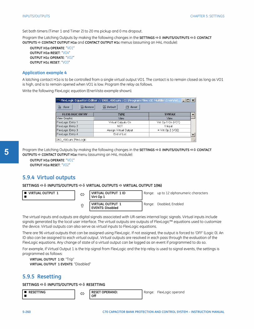
5-260 C70 CAPACITOR BANK PROTECTION AND CONTROL SYSTEM – INSTRUCTION MANUAL
INPUTS/OUTPUTS CHAPTER 5: SETTINGS
5
Set both timers (Timer 1 and Timer 2) to 20 ms pickup and 0 ms dropout.
Program the Latching Outputs by making the following changes in the SETTINGS INPUTS/OUTPUTS CONTACT OUTPUTS CONTACT OUTPUT H1a and CONTACT OUTPUT H1c menus (assuming an H4L module):
OUTPUT H1a OPERATE: “VO1”OUTPUT H1a RESET: “VO4”OUTPUT H1c OPERATE: “VO2”OUTPUT H1c RESET: “VO3”
Application example 4A latching contact H1a is to be controlled from a single virtual output VO1. The contact is to remain closed as long as VO1 is high, and is to remain opened when VO1 is low. Program the relay as follows.
Write the following FlexLogic equation (EnerVista example shown).
Program the Latching Outputs by making the following changes in the SETTINGS INPUTS/OUTPUTS CONTACT OUTPUTS CONTACT OUTPUT H1a menu (assuming an H4L module):
OUTPUT H1a OPERATE: “VO1”OUTPUT H1a RESET: “VO2”
5.9.4 Virtual outputsSETTINGS INPUTS/OUTPUTS VIRTUAL OUTPUTS VIRTUAL OUTPUT 1(96)
The virtual inputs and outputs are digital signals associated with UR-series internal logic signals. Virtual inputs include signals generated by the local user interface. The virtual outputs are outputs of FlexLogic™ equations used to customize the device. Virtual outputs can also serve as virtual inputs to FlexLogic equations.
There are 96 virtual outputs that can be assigned using FlexLogic. If not assigned, the output is forced to ‘OFF’ (Logic 0). An ID also can be assigned to each virtual output. Virtual outputs are resolved in each pass through the evaluation of the FlexLogic equations. Any change of state of a virtual output can be logged as an event if programmed to do so.
For example, if Virtual Output 1 is the trip signal from FlexLogic and the trip relay is used to signal events, the settings is programmed as follows:
VIRTUAL OUTPUT 1 ID: "Trip"VIRTUAL OUTPUT 1 EVENTS: "Disabled"
5.9.5 ResettingSETTINGS INPUTS/OUTPUTS RESETTING
VIRTUAL OUTPUT 1 VIRTUAL OUTPUT 1 ID
Virt Op 1Range: up to 12 alphanumeric characters
VIRTUAL OUTPUT 1EVENTS: Disabled
Range: Disabled, Enabled
RESETTING RESET OPERAND:
OffRange: FlexLogic operand
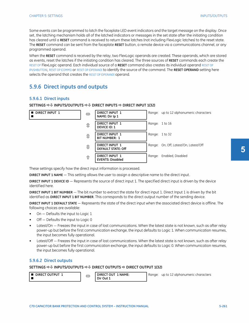
CHAPTER 5: SETTINGS INPUTS/OUTPUTS
C70 CAPACITOR BANK PROTECTION AND CONTROL SYSTEM – INSTRUCTION MANUAL 5-261
5
Some events can be programmed to latch the faceplate LED event indicators and the target message on the display. Once set, the latching mechanism holds all of the latched indicators or messages in the set state after the initiating condition has cleared until a RESET command is received to return these latches (not including FlexLogic latches) to the reset state. The RESET command can be sent from the faceplate RESET button, a remote device via a communications channel, or any programmed operand.
When the RESET command is received by the relay, two FlexLogic operands are created. These operands, which are stored as events, reset the latches if the initiating condition has cleared. The three sources of RESET commands each create the RESET OP FlexLogic operand. Each individual source of a RESET command also creates its individual operand RESET OP (PUSHBUTTON), RESET OP (COMMS) or RESET OP (OPERAND) to identify the source of the command. The RESET OPERAND setting here selects the operand that creates the RESET OP (OPERAND) operand.
5.9.6 Direct inputs and outputs
5.9.6.1 Direct inputsSETTINGS INPUTS/OUTPUTS DIRECT INPUTS DIRECT INPUT 1(32)
These settings specify how the direct input information is processed.
DIRECT INPUT 1 NAME — This setting allows the user to assign a descriptive name to the direct input.
DIRECT INPUT 1 DEVICE ID — Represents the source of direct input 1. The specified direct input is driven by the device identified here.
DIRECT INPUT 1 BIT NUMBER — The bit number to extract the state for direct input 1. Direct Input 1 is driven by the bit identified as DIRECT INPUT 1 BIT NUMBER. This corresponds to the direct output number of the sending device.
DIRECT INPUT 1 DEFAULT STATE — Represents the state of the direct input when the associated direct device is offline. The following choices are available:
• On — Defaults the input to Logic 1
• Off — Defaults the input to Logic 0
• Latest/On — Freezes the input in case of lost communications. When the latest state is not known, such as after relay power-up but before the first communication exchange, the input defaults to Logic 1. When communication resumes, the input becomes fully operational.
• Latest/Off — Freezes the input in case of lost communications. When the latest state is not known, such as after relay power-up but before the first communication exchange, the input defaults to Logic 0. When communication resumes, the input becomes fully operational.
5.9.6.2 Direct outputsSETTINGS INPUTS/OUTPUTS DIRECT OUTPUTS DIRECT OUTPUT 1(32)
DIRECT INPUT 1 DIRECT INPUT 1
NAME: Dir Ip 1Range: up to 12 alphanumeric characters
DIRECT INPUT 1DEVICE ID: 1
Range: 1 to 16
DIRECT INPUT 1BIT NUMBER: 1
Range: 1 to 32
DIRECT INPUT 1DEFAULT STATE: Off
Range: On, Off, Latest/On, Latest/Off
DIRECT INPUT 1EVENTS: Disabled
Range: Enabled, Disabled
DIRECT OUTPUT 1 DIRECT OUT 1 NAME:
Dir Out 1Range: up to 12 alphanumeric characters

5-262 C70 CAPACITOR BANK PROTECTION AND CONTROL SYSTEM – INSTRUCTION MANUAL
INPUTS/OUTPUTS CHAPTER 5: SETTINGS
5
DIRECT OUT 1 NAME — This setting allows the user to assign a descriptive name to the direct output.
DIR OUT 1 OPERAND — This sets the FlexLogic operand that determines the state of this direct output.
5.9.6.3 Application examplesThe examples introduced in the earlier Direct Inputs and Outputs section (part of the Product Setup section) are continued here to illustrate usage of the direct inputs and outputs.
Example 1: Extending input/output capabilities of a UR relayConsider an application that requires additional quantities of contact inputs or output contacts or lines of programmable logic that exceed the capabilities of a single UR-series chassis. The problem is solved by adding an extra UR-series IED, such as the C30, to satisfy the additional inputs/outputs and programmable logic requirements. The figure shows that two IEDs are connected via single-channel digital communication cards.
Figure 5-139: Input and output extension via direct inputs and outputs
Assume that contact input 1 from UR IED 2 is to be used by UR IED 1. The following settings are applied (Direct Input 5 and bit number 12 are used, as an example).
UR IED 1:DIRECT INPUT 5 DEVICE ID = “2”DIRECT INPUT 5 BIT NUMBER = “12”
UR IED 2:DIRECT OUT 12 OPERAND = “Cont Ip 1 On”
The Cont Ip 1 On operand of UR IED 2 is now available in UR IED 1 as DIRECT INPUT 5 ON.
Example 2: Interlocking busbar protectionA simple interlocking busbar protection scheme can be accomplished by sending a blocking signal from downstream devices, say 2, 3 and 4, to the upstream device that monitors a single incomer of the busbar, as shown in the figure.
DIRECT OUT 1 OPERAND:Off
Range: FlexLogic operand
DIRECT OUTPUT 1EVENTS: Disabled
Range: Enabled, Disabled

CHAPTER 5: SETTINGS INPUTS/OUTPUTS
C70 CAPACITOR BANK PROTECTION AND CONTROL SYSTEM – INSTRUCTION MANUAL 5-263
5
Figure 5-140: Sample interlocking busbar protection scheme
Assume that Phase Instantaneous Overcurrent 1 is used by Devices 2, 3, and 4 to block Device 1. If not blocked, Device 1 trips the bus upon detecting a fault and applying a short coordination time delay.
The following settings are applied (assume Bit 3 is used by all 3 devices to send the blocking signal and Direct Inputs 7, 8, and 9 are used by the receiving device to monitor the three blocking signals).
UR IED 2:DIRECT OUT 3 OPERAND: "PHASE IOC1 OP"
UR IED 3:DIRECT OUT 3 OPERAND: "PHASE IOC1 OP"
UR IED 4:DIRECT OUT 3 OPERAND: "PHASE IOC1 OP"
UR IED 1:DIRECT INPUT 7 DEVICE ID: "2"DIRECT INPUT 7 BIT NUMBER: "3"DIRECT INPUT 7 DEFAULT STATE: select "On" for security, select "Off" for dependability
DIRECT INPUT 8 DEVICE ID: "3"DIRECT INPUT 8 BIT NUMBER: "3"DIRECT INPUT 8 DEFAULT STATE: select "On" for security, select "Off" for dependability
DIRECT INPUT 9 DEVICE ID: "4"DIRECT INPUT 9 BIT NUMBER: "3"DIRECT INPUT 9 DEFAULT STATE: select "On" for security, select "Off" for dependability
Now the three blocking signals are available in UR IED 1 as DIRECT INPUT 7 ON, DIRECT INPUT 8 ON, and DIRECT INPUT 9 ON. Upon losing communications or a device, the scheme is inclined to block (if any default state is set to “On”), or to trip the bus on any overcurrent condition (all default states set to “Off”).
Example 3: Pilot-aided schemesConsider a three-terminal line protection application shown in the following figure.
842712A1.CDR
UR IED 1
UR IED 2 UR IED 4UR IED 3
BLOCK
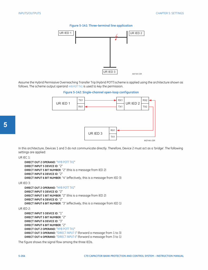
5-264 C70 CAPACITOR BANK PROTECTION AND CONTROL SYSTEM – INSTRUCTION MANUAL
INPUTS/OUTPUTS CHAPTER 5: SETTINGS
5
Figure 5-141: Three-terminal line application
Assume the Hybrid Permissive Overreaching Transfer Trip (Hybrid POTT) scheme is applied using the architecture shown as follows. The scheme output operand HYB POTT TX1 is used to key the permission.
Figure 5-142: Single-channel open-loop configuration
In this architecture, Devices 1 and 3 do not communicate directly. Therefore, Device 2 must act as a ‘bridge’. The following settings are applied:
UR IEC 1:DIRECT OUT 2 OPERAND: "HYB POTT TX1"DIRECT INPUT 5 DEVICE ID: "2"DIRECT INPUT 5 BIT NUMBER: "2" (this is a message from IED 2)DIRECT INPUT 6 DEVICE ID: "2"DIRECT INPUT 6 BIT NUMBER: "4" (effectively, this is a message from IED 3)
UR IED 3:DIRECT OUT 2 OPERAND: "HYB POTT TX1"DIRECT INPUT 5 DEVICE ID: "2"DIRECT INPUT 5 BIT NUMBER: "2" (this is a message from IED 2)DIRECT INPUT 6 DEVICE ID: "2"DIRECT INPUT 6 BIT NUMBER: "3" (effectively, this is a message from IED 1)
UR IED 2:DIRECT INPUT 5 DEVICE ID: "1"DIRECT INPUT 5 BIT NUMBER: "2"DIRECT INPUT 6 DEVICE ID: "3"DIRECT INPUT 6 BIT NUMBER: "2"DIRECT OUT 2 OPERAND: "HYB POTT TX1"DIRECT OUT 3 OPERAND: "DIRECT INPUT 5" (forward a message from 1 to 3)DIRECT OUT 4 OPERAND: "DIRECT INPUT 6" (forward a message from 3 to 1)
The figure shows the signal flow among the three IEDs.
842713A1.CDR
UR IED 1 UR IED 2
UR IED 3
842714A1.CDR
UR IED 1TX1
RX1
UR IED 2RX2
TX2
RX1
TX1
UR IED 3RX1
TX1

CHAPTER 5: SETTINGS TRANSDUCER INPUTS/OUTPUTS
C70 CAPACITOR BANK PROTECTION AND CONTROL SYSTEM – INSTRUCTION MANUAL 5-265
5
Figure 5-143: Signal flow for direct input and output
In three-terminal applications, both the remote terminals must grant permission to trip. Therefore, at each terminal, direct inputs 5 and 6 are ANDed in FlexLogic and the resulting operand configured as the permission to trip (HYB POTT RX1 setting).
5.10 Transducer inputs/outputs
5.10.1 DCmA inputsSETTINGS TRANSDUCER I/O DCMA INPUTS DCMA INPUT F1(U8)
Hardware and software are provided to receive signals from external transducers and to convert these signals into a digital format for use as required. The relay accepts inputs in the range of –1 to +20 mA DC, suitable for use with most common transducer output ranges; all inputs are assumed to be linear over the complete range. Hardware details are contained in chapter 3.
DCMA INPUT F1 DCMA INPUT F1
FUNCTION: DisabledRange: Disabled, Enabled
DCMA INPUT F1 ID:DCMA Ip 1
Range: up to 20 alphanumeric characters
DCMA INPUT F1UNITS: μA
Range: six alphanumeric characters
DCMA INPUT F1RANGE: 0 to -1 mA
Range: 0 to –1 mA, 0 to +1 mA, –1 to +1 mA, 0 to 5 mA, 0 to 10mA, 0 to 20 mA, 4 to 20 m
DCMA INPUT F1 MINVALUE: 0.000
Range: –9999.999 to +9999.999 in steps of 0.001
DCMA INPUT F1 MAXVALUE: 0.000
Range: –9999.999 to +9999.999 in steps of 0.001
The C70 is provided with optional DCmA capability. This feature is specified as an option at the time of ordering. See the Order Codes section in chapter 2 for details.
842717A1.CDR
UR IED 3
UR IED 2UR IED 1
DIRECT OUT 2 = HYB POTT TX1
DIRECT INPUT 5
DIRECT INPUT 6
DIRECT OUT 2 = HYB POTT TX1
DIRECT INPUT 5
DIRECT INPUT 6
DIRECT OUT 2 = HYB POTT TX1
DIRECT INPUT 6
DIRECT OUT 4 = DIRECT INPUT 6
DIRECT OUT 3 = DIRECT INPUT 5
DIRECT INPUT 5
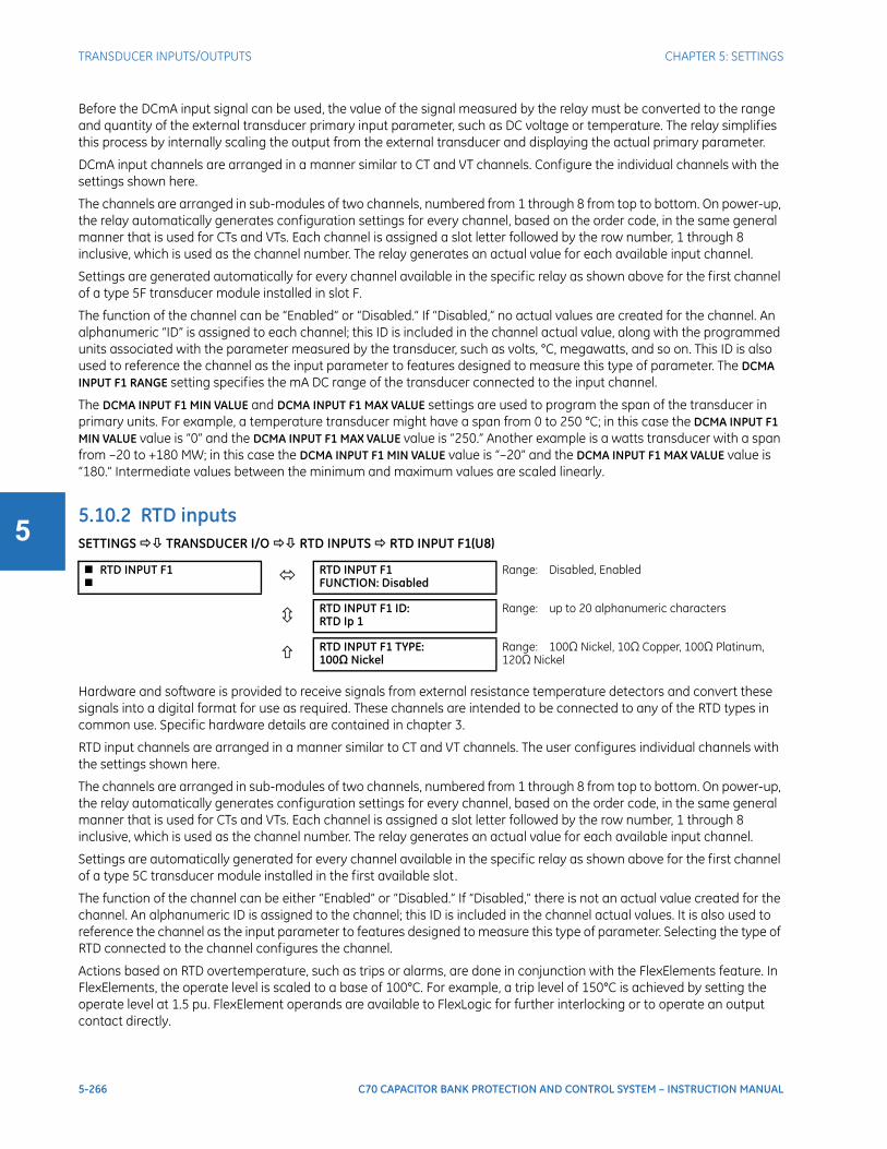
5-266 C70 CAPACITOR BANK PROTECTION AND CONTROL SYSTEM – INSTRUCTION MANUAL
TRANSDUCER INPUTS/OUTPUTS CHAPTER 5: SETTINGS
5
Before the DCmA input signal can be used, the value of the signal measured by the relay must be converted to the range and quantity of the external transducer primary input parameter, such as DC voltage or temperature. The relay simplifies this process by internally scaling the output from the external transducer and displaying the actual primary parameter.
DCmA input channels are arranged in a manner similar to CT and VT channels. Configure the individual channels with the settings shown here.
The channels are arranged in sub-modules of two channels, numbered from 1 through 8 from top to bottom. On power-up, the relay automatically generates configuration settings for every channel, based on the order code, in the same general manner that is used for CTs and VTs. Each channel is assigned a slot letter followed by the row number, 1 through 8 inclusive, which is used as the channel number. The relay generates an actual value for each available input channel.
Settings are generated automatically for every channel available in the specific relay as shown above for the first channel of a type 5F transducer module installed in slot F.
The function of the channel can be “Enabled” or “Disabled.” If “Disabled,” no actual values are created for the channel. An alphanumeric “ID” is assigned to each channel; this ID is included in the channel actual value, along with the programmed units associated with the parameter measured by the transducer, such as volts, °C, megawatts, and so on. This ID is also used to reference the channel as the input parameter to features designed to measure this type of parameter. The DCMA INPUT F1 RANGE setting specifies the mA DC range of the transducer connected to the input channel.
The DCMA INPUT F1 MIN VALUE and DCMA INPUT F1 MAX VALUE settings are used to program the span of the transducer in primary units. For example, a temperature transducer might have a span from 0 to 250 °C; in this case the DCMA INPUT F1 MIN VALUE value is “0” and the DCMA INPUT F1 MAX VALUE value is “250.” Another example is a watts transducer with a span from –20 to +180 MW; in this case the DCMA INPUT F1 MIN VALUE value is “–20” and the DCMA INPUT F1 MAX VALUE value is “180.” Intermediate values between the minimum and maximum values are scaled linearly.
5.10.2 RTD inputsSETTINGS TRANSDUCER I/O RTD INPUTS RTD INPUT F1(U8)
Hardware and software is provided to receive signals from external resistance temperature detectors and convert these signals into a digital format for use as required. These channels are intended to be connected to any of the RTD types in common use. Specific hardware details are contained in chapter 3.
RTD input channels are arranged in a manner similar to CT and VT channels. The user configures individual channels with the settings shown here.
The channels are arranged in sub-modules of two channels, numbered from 1 through 8 from top to bottom. On power-up, the relay automatically generates configuration settings for every channel, based on the order code, in the same general manner that is used for CTs and VTs. Each channel is assigned a slot letter followed by the row number, 1 through 8 inclusive, which is used as the channel number. The relay generates an actual value for each available input channel.
Settings are automatically generated for every channel available in the specific relay as shown above for the first channel of a type 5C transducer module installed in the first available slot.
The function of the channel can be either “Enabled” or “Disabled.” If “Disabled,” there is not an actual value created for the channel. An alphanumeric ID is assigned to the channel; this ID is included in the channel actual values. It is also used to reference the channel as the input parameter to features designed to measure this type of parameter. Selecting the type of RTD connected to the channel configures the channel.
Actions based on RTD overtemperature, such as trips or alarms, are done in conjunction with the FlexElements feature. In FlexElements, the operate level is scaled to a base of 100°C. For example, a trip level of 150°C is achieved by setting the operate level at 1.5 pu. FlexElement operands are available to FlexLogic for further interlocking or to operate an output contact directly.
RTD INPUT F1 RTD INPUT F1
FUNCTION: DisabledRange: Disabled, Enabled
RTD INPUT F1 ID:RTD Ip 1
Range: up to 20 alphanumeric characters
RTD INPUT F1 TYPE:100Ω Nickel
Range: 100Ω Nickel, 10Ω Copper, 100Ω Platinum, 120Ω Nickel

CHAPTER 5: SETTINGS TRANSDUCER INPUTS/OUTPUTS
C70 CAPACITOR BANK PROTECTION AND CONTROL SYSTEM – INSTRUCTION MANUAL 5-267
5
See the following table for reference temperature values for each RTD type.
Table 5-36: RTD temperature vs. resistance
5.10.3 DCmA outputsSETTINGS TRANSDUCER I/O DCMA OUTPUTS DCMA OUTPUT F1(U8)
Temperature Resistance (in ohms)
°C °F 100 Ω Pt (DIN 43760)
120 Ω Ni 100 Ω Ni 10 Ω Cu
–50 –58 80.31 86.17 71.81 7.10
–40 –40 84.27 92.76 77.30 7.49
–30 –22 88.22 99.41 82.84 7.88
–20 –4 92.16 106.15 88.45 8.26
–10 14 96.09 113.00 94.17 8.65
0 32 100.00 120.00 100.00 9.04
10 50 103.90 127.17 105.97 9.42
20 68 107.79 134.52 112.10 9.81
30 86 111.67 142.06 118.38 10.19
40 104 115.54 149.79 124.82 10.58
50 122 119.39 157.74 131.45 10.97
60 140 123.24 165.90 138.25 11.35
70 158 127.07 174.25 145.20 11.74
80 176 130.89 182.84 152.37 12.12
90 194 134.70 191.64 159.70 12.51
100 212 138.50 200.64 167.20 12.90
110 230 142.29 209.85 174.87 13.28
120 248 146.06 219.29 182.75 13.67
130 266 149.82 228.96 190.80 14.06
140 284 153.58 238.85 199.04 14.44
150 302 157.32 248.95 207.45 14.83
160 320 161.04 259.30 216.08 15.22
170 338 164.76 269.91 224.92 15.61
180 356 168.47 280.77 233.97 16.00
190 374 172.46 291.96 243.30 16.39
200 392 175.84 303.46 252.88 16.78
210 410 179.51 315.31 262.76 17.17
220 428 183.17 327.54 272.94 17.56
230 446 186.82 340.14 283.45 17.95
240 464 190.45 353.14 294.28 18.34
250 482 194.08 366.53 305.44 18.73
DCMA OUTPUT F1 DCMA OUTPUT F1
SOURCE: OffRange: Off, any analog actual value parameter
DCMA OUTPUT F1RANGE: –1 to 1 mA
Range: –1 to 1 mA, 0 to 1 mA, 4 to 20 mA
DCMA OUTPUT F1MIN VAL: 0.000 pu
Range: –90.000 to 90.000 pu in steps of 0.001
DCMA OUTPUT F1MAX VAL: 1.000 pu
Range: –90.000 to 90.000 pu in steps of 0.001
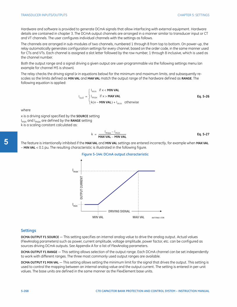
5-268 C70 CAPACITOR BANK PROTECTION AND CONTROL SYSTEM – INSTRUCTION MANUAL
TRANSDUCER INPUTS/OUTPUTS CHAPTER 5: SETTINGS
5
Hardware and software is provided to generate DCmA signals that allow interfacing with external equipment. Hardware details are contained in chapter 3. The DCmA output channels are arranged in a manner similar to transducer input or CT and VT channels. The user configures individual channels with the settings as follows.
The channels are arranged in sub-modules of two channels, numbered 1 through 8 from top to bottom. On power-up, the relay automatically generates configuration settings for every channel, based on the order code, in the same manner used for CTs and VTs. Each channel is assigned a slot letter followed by the row number, 1 through 8 inclusive, which is used as the channel number.
Both the output range and a signal driving a given output are user-programmable via the following settings menu (an example for channel M5 is shown).
The relay checks the driving signal (x in equations below) for the minimum and maximum limits, and subsequently re-scales so the limits defined as MIN VAL and MAX VAL match the output range of the hardware defined as RANGE. The following equation is applied:
Eq. 5-26
where
x is a driving signal specified by the SOURCE settingImin and Imax are defined by the RANGE settingk is a scaling constant calculated as:
Eq. 5-27
The feature is intentionally inhibited if the MAX VAL and MIN VAL settings are entered incorrectly, for example when MAX VAL – MIN VAL < 0.1 pu. The resulting characteristic is illustrated in the following figure.
Figure 5-144: DCmA output characteristic
SettingsDCMA OUTPUT F1 SOURCE — This setting specifies an internal analog value to drive the analog output. Actual values (FlexAnalog parameters) such as power, current amplitude, voltage amplitude, power factor, etc. can be configured as sources driving DCmA outputs. See Appendix A for a list of FlexAnalog parameters.
DCMA OUTPUT F1 RANGE — This setting allows selection of the output range. Each DCmA channel can be set independently to work with different ranges. The three most commonly used output ranges are available.
DCMA OUTPUT F1 MIN VAL — This setting allows setting the minimum limit for the signal that drives the output. This setting is used to control the mapping between an internal analog value and the output current. The setting is entered in per-unit values. The base units are defined in the same manner as the FlexElement base units.
Iout
Imin if x MIN VAL<
Imax if x MAX VAL>
k x MIN VAL–( ) Imin+ otherwise
=
kImax Imin–
MAX VAL MIN VAL–--------------------------------------------=
842739A1.CDR
DRIVING SIGNAL
OU
TPU
T CU
RREN
T
MIN VAL
Imin
Imax
MAX VAL

CHAPTER 5: SETTINGS TRANSDUCER INPUTS/OUTPUTS
C70 CAPACITOR BANK PROTECTION AND CONTROL SYSTEM – INSTRUCTION MANUAL 5-269
5
DCMA OUTPUT F1 MAX VAL — This setting allows setting the maximum limit for the signal that drives the output. This setting is used to control the mapping between an internal analog value and the output current. The setting is entered in per-unit values. The base units are defined in the same manner as the FlexElement base units.
Three application examples follow.
Example: Power monitoringA three phase active power on a 13.8 kV system measured via UR-series relay source 1 is to be monitored by the DCmA H1 output of the range of –1 to 1 mA. The following settings are applied on the relay: CT ratio = 1200:5, VT secondary 115, VT connection is delta, and VT ratio = 120. The nominal current is 800 A primary and the nominal power factor is 0.90. The power is to be monitored in both importing and exporting directions and allow for 20% overload compared to the nominal.
The nominal three-phase power is:
Eq. 5-28
The three-phase power with 20% overload margin is:
Eq. 5-29
The base unit for power (refer to the FlexElements section in this chapter for additional details) is:
Eq. 5-30
The minimum and maximum power values to be monitored (in pu) are:
Eq. 5-31
The following settings are entered:DCMA OUTPUT H1 SOURCE: “SRC 1 P”DCMA OUTPUT H1 RANGE: “–1 to 1 mA”DCMA OUTPUT H1 MIN VAl: “–1.247 pu”DCMA OUTPUT H1 MAX VAL: “1.247 pu”
With the above settings, the output will represent the power with the scale of 1 mA per 20.65 MW. The worst-case error for this application can be calculated by superimposing the following two sources of error:
• ±0.5% of the full scale for the analog output module, or
• ±1% of reading error for the active power at power factor of 0.9
For example at the reading of 20 MW, the worst-case error is 0.01 × 20 MW + 0.207 MW = 0.407 MW.
Example: Current monitoringThe phase A current (true RMS value) is to be monitored via the H2 current output working with the range from 4 to 20 mA. The CT ratio is 5000:5 and the maximum load current is 4200 A. The current is to be monitored from 0 A upwards, allowing for 50% overload.
The phase current with the 50% overload margin is:
Eq. 5-32
The base unit for current (see the FlexElements section in this chapter for additional details) is:
Eq. 5-33
The minimum and maximum power values to be monitored (in pu) are:
Eq. 5-34
NOTE
The DCMA OUTPUT F1 MIN VAL and DCMA OUTPUT F1 MAX VAL settings are ignored for power factor base units (i.e. if the DCMA OUTPUT F1 SOURCE is set to FlexAnalog value based on power factor measurement).
P 3 13.8 kV 0.8 kA× 0.9×× 17.21 MW= =
Pmax 1.2 17.21 MW× 20.65 MW= =
PBASE 115 V 120× 1.2 kA× 16.56 MW= =
minimum power 20.65 MW–16.56 MW
-------------------------- 1.247 pu, maximum power 20.65 MW16.56 MW----------------------- 1.247 pu= =–= =
0.005± 1 1–( )–( ) 20.65 MW×× 0.207 MW±=
Imax 1.5 4.2 kA× 6.3 kA= =
IBASE 5 kA=
minimum current 0 kA5 kA---------- 0 pu, maximum current 6.3 kA
5 kA-------------- 1.26 pu= == =

5-270 C70 CAPACITOR BANK PROTECTION AND CONTROL SYSTEM – INSTRUCTION MANUAL
TESTING CHAPTER 5: SETTINGS
5
The following settings are entered:DCMA OUTPUT H2 SOURCE: “SRC 1 Ia RMS”DCMA OUTPUT H2 RANGE: “4 to 20 mA”DCMA OUTPUT H2 MIN VAL: “0.000 pu”DCMA OUTPUT H2 MAX VAL: “1.260 pu”
The worst-case error for this application can be calculated by superimposing the following two sources of error:
• ±0.5% of the full scale for the analog output module, or
• ±0.25% of reading or ±0.1% of rated (whichever is greater) for currents between 0.1 and 2.0 of nominal
For example, at the reading of 4.2 kA, the worst-case error is max(0.0025 × 4.2 kA, 0.001 × 5 kA) + 0.504 kA = 0.515 kA.
Example: Voltage monitoringA positive-sequence voltage on a 400 kV system measured via source 2 is to be monitored by the DCmA H3 output with a range of 0 to 1 mA. The VT secondary setting is 66.4 V, the VT ratio setting is 6024, and the VT connection setting is “Delta.” The voltage is to be monitored in the range from 70% to 110% of nominal.
The minimum and maximum positive-sequence voltages to be monitored are:
Eq. 5-35
The base unit for voltage (see the FlexElements section in this chapter for additional details) is:
Eq. 5-36
The minimum and maximum voltage values to be monitored (in pu) are:
Eq. 5-37
The following settings are entered:DCMA OUTPUT H3 SOURCE: “SRC 2 V_1 mag”DCMA OUTPUT H3 RANGE: “0 to 1 mA”DCMA OUTPUT H3 MIN VAL: “0.404 pu”DCMA OUTPUT H3 MAX VAL: “0.635 pu”
The limit settings differ from the expected 0.7 pu and 1.1 pu because the relay calculates the positive-sequence quantities scaled to the phase-to-ground voltages, even if the VTs are connected in “Delta” (see the Metering Conventions section in chapter 6), while at the same time the VT nominal voltage is 1 pu for the settings. Consequently the settings required in this example differ from naturally expected by the factor of .
The worst-case error for this application could be calculated by superimposing the following two sources of error:
• ±0.5% of the full scale for the analog output module, or
• ±0.5% of reading
For example, under nominal conditions, the positive-sequence reads 230.94 kV and the worst-case error is 0.005 × 230.94 kV + 1.27 kV = 2.42 kV.
5.11 Testing
5.11.1 Test mode functionSETTINGS TESTING TEST MODE FUNCTION
TESTING TEST MODE
FUNCTION: DisabledRange: Disabled, Isolated, Forcible
0.005 20 4–( ) 6.3 kA××± 0.504 kA±=
Vmin 0.7 400 kV
3----------------× 161.66 kV, Vmax 1.1 400 kV
3----------------× 254.03 kV= == =
VBASE 0.0664 kV 6024× 400 kV= =
minimum voltage 161.66 kV400 kV
----------------------- 0.404 pu, maximum voltage 254.03 kV400 kV
----------------------- 0.635 pu= == =
3
0.005 1 0–( )× 254.03 kV×± 1.27 kV±=

CHAPTER 5: SETTINGS TESTING
C70 CAPACITOR BANK PROTECTION AND CONTROL SYSTEM – INSTRUCTION MANUAL 5-271
5
The C70 provides a test facility to verify the functionality of contact inputs and outputs, some communication channels and the phasor measurement unit (where applicable), using simulated conditions.
The test mode can be in any of three states: Disabled, Isolated, or Forcible.
The Disabled mode is intended for normal in service operation; relay protection, control and communication function is normal. Test features are disabled, except channel tests and phasor measurement unit tests remain usable when provided.
The Isolated mode is intended to allow the relay to be quickly placed in a state where the relay cannot negatively impact the power system or other parts of the substation automation system. This is to allow changing settings, loading new firmware, changing hardware modules, and changing communication connections. As far as practical all relay output signals are blocked. Contact outputs are de-energized, latching outputs are frozen. Commands to bricks are blocked. GOOSE transmissions have their "simulation" flag (also known as "test" flag) set, which results in the messages not being accepted by compliant receiving devices that do not have a "Sim" data attribute set. The quality attribute of values that can be output via 61850 MMS services are set to "invalid," which results in the values not being used for operational purposes by compliant receiving devices.
The Forcible mode is intended for testing involving forcing relay operation by test signal injection and verifying correct relay output. This mode is also for tests to verify the relay outputs (both contact and communications) have the intended impact on specific power system devices or on specific other substation automation devices. Contact outputs can be selectively enabled or forced as described in the following two sections. Shared outputs to bricks have their test mode flag raised, which results in their value only being accepted by relays also in forcible mode. GOOSE transmissions have the "simulation" flag set, which results in these only being accepted by other devices that have their "Sim" data attribute set. The "Sim" data attribute in the relay is set, so that if GOOSE messages are received with the "simulation" flag set, these are used in place of the normal messages. The quality attribute of values that are output via 61850 MMS services are set to "valid" + "test," which signals that the values should not be used for operational purposes.
Otherwise, the UR remains fully operational while in the Forcible test mode, allowing for various testing procedures. In particular, the protection and control elements, and FlexLogic function normally. Other than the IEC 61850 protocol, communications based inputs and outputs remain fully operational. The test procedure must take this into account.
The test mode can be selected either through the front panel, through EnerVista UR Setup, or through IEC 61850 control to LLN0.Mod. LLN0.Mod.ctlVal "on" selects Disabled, "test/blocked" selects Isolated, and "test" selects Forcible. The TEST MODE FUNCTION setting can only be changed by a direct user command. Following a restart, power up, settings upload, or firmware upgrade, the test mode remains at the last programmed value. This allows a UR that has been placed in isolated mode to remain isolated during testing and maintenance activities.
5.11.2 Test mode forcingSETTINGS TESTING TEST MODE FORCING
The test mode state is indicated on the relay faceplate by a combination of the Test Mode LED indicator, the In-Service LED indicator, and by the critical fail relay, as shown in the following table.
Table 5-37: Test mode operation
TESTING TEST MODE FORCING:
OnRange: FlexLogic operand
Test mode function
In-service LED
Test mode LED
Critical fail relay
Test mode forcing Contact input and output behavior
Disabled Unaffected Off Normal No effect Normal
Isolated Off On De-energized No effect Contact outputs disabled
Forcible Off Flashing De-energized Off Normal
On Controlled by forcing features
NOTE
On restart, the TEST MODE FORCING setting and the force contact input and force contact output settings revert to their default states.
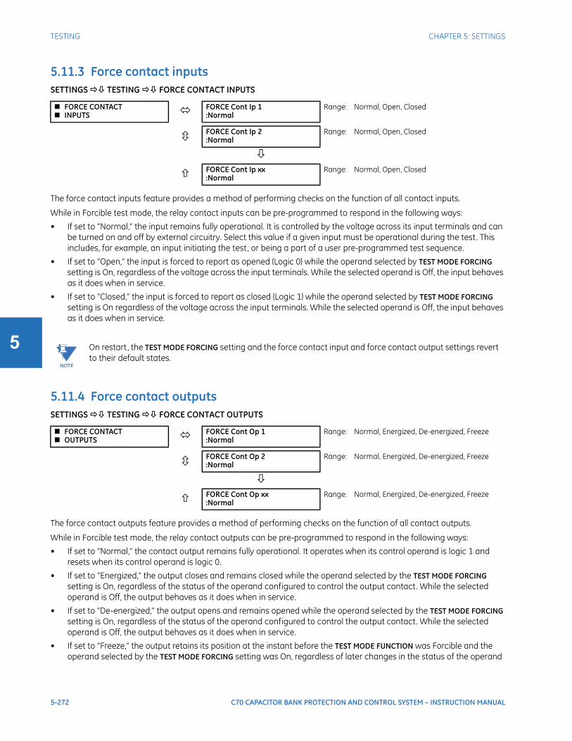
5-272 C70 CAPACITOR BANK PROTECTION AND CONTROL SYSTEM – INSTRUCTION MANUAL
TESTING CHAPTER 5: SETTINGS
5
5.11.3 Force contact inputsSETTINGS TESTING FORCE CONTACT INPUTS
The force contact inputs feature provides a method of performing checks on the function of all contact inputs.
While in Forcible test mode, the relay contact inputs can be pre-programmed to respond in the following ways:
• If set to “Normal,” the input remains fully operational. It is controlled by the voltage across its input terminals and can be turned on and off by external circuitry. Select this value if a given input must be operational during the test. This includes, for example, an input initiating the test, or being a part of a user pre-programmed test sequence.
• If set to “Open,” the input is forced to report as opened (Logic 0) while the operand selected by TEST MODE FORCING setting is On, regardless of the voltage across the input terminals. While the selected operand is Off, the input behaves as it does when in service.
• If set to “Closed,” the input is forced to report as closed (Logic 1) while the operand selected by TEST MODE FORCING setting is On regardless of the voltage across the input terminals. While the selected operand is Off, the input behaves as it does when in service.
5.11.4 Force contact outputsSETTINGS TESTING FORCE CONTACT OUTPUTS
The force contact outputs feature provides a method of performing checks on the function of all contact outputs.
While in Forcible test mode, the relay contact outputs can be pre-programmed to respond in the following ways:
• If set to “Normal,” the contact output remains fully operational. It operates when its control operand is logic 1 and resets when its control operand is logic 0.
• If set to “Energized,” the output closes and remains closed while the operand selected by the TEST MODE FORCING setting is On, regardless of the status of the operand configured to control the output contact. While the selected operand is Off, the output behaves as it does when in service.
• If set to “De-energized,” the output opens and remains opened while the operand selected by the TEST MODE FORCING setting is On, regardless of the status of the operand configured to control the output contact. While the selected operand is Off, the output behaves as it does when in service.
• If set to “Freeze,” the output retains its position at the instant before the TEST MODE FUNCTION was Forcible and the operand selected by the TEST MODE FORCING setting was On, regardless of later changes in the status of the operand
FORCE CONTACT INPUTS FORCE Cont Ip 1
:NormalRange: Normal, Open, Closed
FORCE Cont Ip 2:Normal
Range: Normal, Open, Closed
FORCE Cont Ip xx:Normal
Range: Normal, Open, Closed
NOTE
On restart, the TEST MODE FORCING setting and the force contact input and force contact output settings revert to their default states.
FORCE CONTACT OUTPUTS FORCE Cont Op 1
:NormalRange: Normal, Energized, De-energized, Freeze
FORCE Cont Op 2:Normal
Range: Normal, Energized, De-energized, Freeze
FORCE Cont Op xx:Normal
Range: Normal, Energized, De-energized, Freeze

CHAPTER 5: SETTINGS TESTING
C70 CAPACITOR BANK PROTECTION AND CONTROL SYSTEM – INSTRUCTION MANUAL 5-273
5
configured to control the output contact. While the selected operand is Off, the output behaves as it does when in service.
NOTE
On restart, the TEST MODE FORCING setting and the force contact input and force contact output settings revert to their default states.

5-274 C70 CAPACITOR BANK PROTECTION AND CONTROL SYSTEM – INSTRUCTION MANUAL
TESTING CHAPTER 5: SETTINGS
5
C70 CAPACITOR BANK PROTECTION AND CONTROL SYSTEM – INSTRUCTION MANUAL 6-1
C70 Capacitor Bank Protection and Control System
Chapter 6: Actual values
Actual values
This chapter outlines viewing of data on the front panel and in the software.
6.1 Actual values menu
ACTUAL VALUES STATUS CONTACT INPUTS
See page 6-3
VIRTUAL INPUTS
See page 6-3
RxGOOSE BOOLEAN INPUTS
See page 6-3
RxGOOSE DPS INPUTS
See page 6-4
CONTACT OUTPUTS
See page 6-4
VIRTUAL OUTPUTS
See page 6-4
RxGOOSE STATUS
See page 6-4
RxGOOSE STATISTICS
See page 6-5
DIGITAL COUNTERS
See page 6-5
SELECTOR SWITCHES
See page 6-5
TIME OF DAY TIMERS
See page 6-6
FLEX STATES
See page 6-6
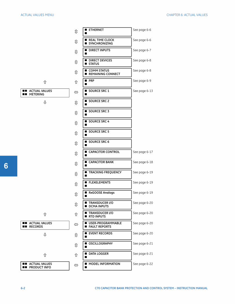
6-2 C70 CAPACITOR BANK PROTECTION AND CONTROL SYSTEM – INSTRUCTION MANUAL
ACTUAL VALUES MENU CHAPTER 6: ACTUAL VALUES
6
ETHERNET
See page 6-6
REAL TIME CLOCK SYNCHRONIZING
See page 6-6
DIRECT INPUTS
See page 6-7
DIRECT DEVICES STATUS
See page 6-8
COMM STATUS REMAINING CONNECT
See page 6-8
PRP
See page 6-9
ACTUAL VALUES METERING SOURCE SRC 1
See page 6-13
SOURCE SRC 2
SOURCE SRC 3
SOURCE SRC 4
SOURCE SRC 5
SOURCE SRC 6
CAPACITOR CONTROL
See page 6-17
CAPACITOR BANK
See page 6-18
TRACKING FREQUENCY
See page 6-19
FLEXELEMENTS
See page 6-19
RxGOOSE Analogs
See page 6-19
TRANSDUCER I/O DCMA INPUTS
See page 6-20
TRANSDUCER I/O RTD INPUTS
See page 6-20
ACTUAL VALUES RECORDS USER-PROGRAMMABLE
FAULT REPORTSSee page 6-20
EVENT RECORDS
See page 6-20
OSCILLOGRAPHY
See page 6-21
DATA LOGGER
See page 6-21
ACTUAL VALUES PRODUCT INFO MODEL INFORMATION
See page 6-22
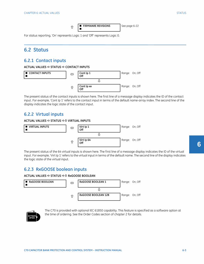
CHAPTER 6: ACTUAL VALUES STATUS
C70 CAPACITOR BANK PROTECTION AND CONTROL SYSTEM – INSTRUCTION MANUAL 6-3
6
For status reporting, ‘On’ represents Logic 1 and ‘Off’ represents Logic 0.
6.2 Status
6.2.1 Contact inputsACTUAL VALUES STATUS CONTACT INPUTS
The present status of the contact inputs is shown here. The first line of a message display indicates the ID of the contact input. For example, ‘Cont Ip 1’ refers to the contact input in terms of the default name-array index. The second line of the display indicates the logic state of the contact input.
6.2.2 Virtual inputsACTUAL VALUES STATUS VIRTUAL INPUTS
The present status of the 64 virtual inputs is shown here. The first line of a message display indicates the ID of the virtual input. For example, ‘Virt Ip 1’ refers to the virtual input in terms of the default name. The second line of the display indicates the logic state of the virtual input.
6.2.3 RxGOOSE boolean inputsACTUAL VALUES STATUS RxGOOSE BOOLEAN
FIRMWARE REVISIONS
See page 6-22
CONTACT INPUTS Cont Ip 1
OffRange: On, Off
Cont Ip xxOff
Range: On, Off
VIRTUAL INPUTS Virt Ip 1
OffRange: On, Off
Virt Ip 64Off
Range: On, Off
RxGOOSE BOOLEAN RxGOOSE BOOLEAN 1 Range: On, Off
RxGOOSE BOOLEAN 128 Range: On, Off
The C70 is provided with optional IEC 61850 capability. This feature is specified as a software option at the time of ordering. See the Order Codes section of chapter 2 for details.

6-4 C70 CAPACITOR BANK PROTECTION AND CONTROL SYSTEM – INSTRUCTION MANUAL
STATUS CHAPTER 6: ACTUAL VALUES
6
6.2.4 RxGOOSE DPS inputsACTUAL VALUES STATUS RxGOOSE DPS
6.2.5 Contact outputsACTUAL VALUES STATUS CONTACT OUTPUTS
The present state of the contact outputs is shown here. The first line of a message display indicates the ID of the contact output. For example, ‘Cont Op 1’ refers to the contact output in terms of the default name-array index. The second line of the display indicates the logic state of the contact output.
For form-A contact outputs, the state of the voltage and current detectors is displayed as Off, VOff, IOff, On, IOn, and VOn. For form-C contact outputs, the state is displayed as Off or On.
6.2.6 Virtual outputsACTUAL VALUES STATUS VIRTUAL OUTPUTS
The present state of up to 96 virtual outputs is shown here. The first line of a message display indicates the ID of the virtual output. For example, ‘Virt Op 1’ refers to the virtual output in terms of the default name-array index. The second line of the display indicates the logic state of the virtual output, as calculated by the FlexLogic equation for that output.
6.2.7 RxGOOSE statusACTUAL VALUES STATUS RxGOOSE STATUS
RxGOOSE DPS RxGOOSE DPS 1 Range: On, Off, Intermediate, Bad
RxGOOSE DPS 5 Range: On, Off, Intermediate, Bad
The C70 is provided with optional IEC 61850 capability. This feature is specified as a software option at the time of ordering. See the Order Codes section of chapter 2 for details.
CONTACT OUTPUTS Cont Op 1
OffRange: On, Off, VOff, VOn, IOn, IOff
Cont Op xxOff
Range: On, Off, VOff, VOn, IOn, IOff
VIRTUAL OUTPUTS Virt Op 1
OffRange: On, Off
Virt Op 96Off
Range: On, Off
RxGOOSE STATUS All RxGOOSE Online:
YesRange: Yes, No
RxGOOSE 1:Off
Range: On, Off

CHAPTER 6: ACTUAL VALUES STATUS
C70 CAPACITOR BANK PROTECTION AND CONTROL SYSTEM – INSTRUCTION MANUAL 6-5
6
The All RxGOOSE Online actual value does not consider RxGOOSE that are not configured or are not used by any RxGOOSE Input.
6.2.8 RxGOOSE statisticsACTUAL VALUES STATUS RxGOOSE STATISTICS RxGOOSE 1(16)
stNum — State number. The most recently received value in GOOSE message field stNum. The publisher increments stNum each time that the state of one or more of the GOOSE message members is sent with a revised value.
sqNum — Sequence number. The most recently received value in GOOSE message field sqNum. The publisher sets sqNum to zero each time the state of one or more of the GOOSE message members is sent with a new value, and it increments it whenever a GOOSE message is resent without any member value change.
6.2.9 Digital countersACTUAL VALUES STATUS DIGITAL COUNTERS DIGITAL COUNTERS Counter 1(8)
The present status of the eight digital counters displays here. The status of each counter, with the user-defined counter name, includes the accumulated and frozen counts (the count units label also appears). Also included, is the date and time stamp for the frozen count. The COUNTER 1 MICROS value refers to the microsecond portion of the time stamp.
6.2.10 Selector switchesACTUAL VALUES STATUS SELECTOR SWITCHES
RxGOOSE 16:Off
Range: On, Off
The C70 is provided with optional IEC 61850 capability. This feature is specified as a software option at the time of ordering. See the Order Codes section of chapter 2 for details.
RxGOOSE 1 RxGOOSE 1
stNum: 0
RxGOOSE 1sqNum: 0
The C70 is provided with optional IEC 61850 capability. This feature is specified as a software option at the time of ordering. See the Order Codes section of chapter 2 for details.
DIGITAL COUNTERS Counter 1 Counter 1 ACCUM:
0
Counter 1 FROZEN:0
Counter 1 FROZEN:YYYY/MM/DD HH:MM:SS
Counter 1 MICROS:0
SELECTOR SWITCHES SELECTOR SWITCH 1
POSITION: 0/7Range: Current Position / 7
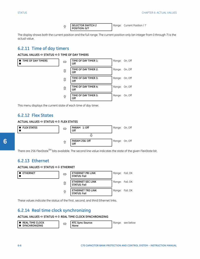
6-6 C70 CAPACITOR BANK PROTECTION AND CONTROL SYSTEM – INSTRUCTION MANUAL
STATUS CHAPTER 6: ACTUAL VALUES
6
The display shows both the current position and the full range. The current position only (an integer from 0 through 7) is the actual value.
6.2.11 Time of day timersACTUAL VALUES STATUS TIME OF DAY TIMERS
This menu displays the current state of each time of day timer.
6.2.12 Flex StatesACTUAL VALUES STATUS FLEX STATES
There are 256 FlexStateTM bits available. The second line value indicates the state of the given FlexState bit.
6.2.13 EthernetACTUAL VALUES STATUS ETHERNET
These values indicate the status of the first, second, and third Ethernet links.
6.2.14 Real time clock synchronizingACTUAL VALUES STATUS REAL TIME CLOCK SYNCHRONIZING
SELECTOR SWITCH 2POSITION: 0/7
Range: Current Position / 7
TIME OF DAY TIMERS TIME OF DAY TIMER 1:
OffRange: On, Off
TIME OF DAY TIMER 2:Off
Range: On, Off
TIME OF DAY TIMER 3:Off
Range: On, Off
TIME OF DAY TIMER 4:Off
Range: On, Off
TIME OF DAY TIMER 5:Off
Range: On, Off
FLEX STATES PARAM 1: Off
OffRange: On, Off
PARAM 256: OffOff
Range: On, Off
ETHERNET ETHERNET PRI LINK
STATUS: FailRange: Fail, OK
ETHERNET SEC LINKSTATUS: Fail
Range: Fail, OK
ETHERNET TRD LINKSTATUS: Fail
Range: Fail, OK
REAL TIME CLOCK SYNCHRONIZING RTC Sync Source:
NoneRange: see below
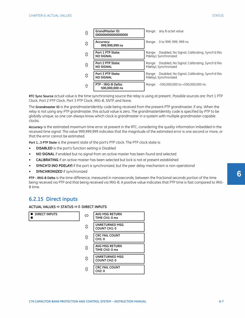
CHAPTER 6: ACTUAL VALUES STATUS
C70 CAPACITOR BANK PROTECTION AND CONTROL SYSTEM – INSTRUCTION MANUAL 6-7
6
RTC Sync Source actual value is the time synchronizing source the relay is using at present. Possible sources are: Port 1 PTP Clock, Port 2 PTP Clock, Port 3 PTP Clock, IRIG-B, SNTP, and None.
The Grandmaster ID is the grandmasterIdentity code being received from the present PTP grandmaster, if any. When the relay is not using any PTP grandmaster, this actual value is zero. The grandmasterIdentity code is specified by PTP to be globally unique, so one can always know which clock is grandmaster in a system with multiple grandmaster-capable clocks.
Accuracy is the estimated maximum time error at present in the RTC, considering the quality information imbedded in the received time signal. The value 999,999,999 indicates that the magnitude of the estimated error is one second or more, or that the error cannot be estimated.
Port 1…3 PTP State is the present state of the port’s PTP clock. The PTP clock state is:
• DISABLED is the port’s function setting is Disabled
• NO SIGNAL if enabled but no signal from an active master has been found and selected
• CALIBRATING if an active master has been selected but lock is not at present established
• SYNCH’D (NO PDELAY) if the port is synchronized, but the peer delay mechanism is non-operational
• SYNCHRONIZED if synchronized
PTP - IRIG-B Delta is the time difference, measured in nanoseconds, between the fractional seconds portion of the time being received via PTP and that being received via IRIG-B. A positive value indicates that PTP time is fast compared to IRIG-B time.
6.2.15 Direct inputsACTUAL VALUES STATUS DIRECT INPUTS
GrandMaster ID:0X0000000000000000
Range: any 8 octet value
Accuracy:999,999,999 ns
Range: 0 to 999, 999, 999 ns
Port 1 PTP State:NO SIGNAL
Range: Disabled, No Signal, Calibrating, Synch’d (No Pdelay), Synchronized
Port 2 PTP State:NO SIGNAL
Range: Disabled, No Signal, Calibrating, Synch’d (No Pdelay), Synchronized
Port 3 PTP State:NO SIGNAL
Range: Disabled, No Signal, Calibrating, Synch’d (No Pdelay), Synchronized
PTP - IRIG-B Delta:500,000,000 ns
Range: -500,000,000 to +500,000,000 ns
DIRECT INPUTS AVG MSG RETURN
TIME CH1: 0 ms
UNRETURNED MSGCOUNT CH1: 0
CRC FAIL COUNTCH1: 0
AVG MSG RETURNTIME CH2: 0 ms
UNRETURNED MSGCOUNT CH2: 0
CRC FAIL COUNTCH2: 0

6-8 C70 CAPACITOR BANK PROTECTION AND CONTROL SYSTEM – INSTRUCTION MANUAL
STATUS CHAPTER 6: ACTUAL VALUES
6
The AVERAGE MSG RETURN TIME is the time taken for direct output messages to return to the sender in a direct input/output ring configuration (this value is not applicable for non-ring configurations). This is a rolling average calculated for the last ten messages. There are two return times for dual-channel communications modules.
The UNRETURNED MSG COUNT values (one per communications channel) count the direct output messages that do not make the trip around the communications ring. The CRC FAIL COUNT values (one per communications channel) count the direct output messages that have been received but fail the CRC check. High values for either of these counts can indicate on a problem with wiring, the communication channel, or one or more relays. The UNRETURNED MSG COUNT and CRC FAIL COUNT values can be cleared using the CLEAR DIRECT I/O COUNTERS command.
The DIRECT INPUT 1 to DIRECT INPUT (32) values represent the state of each direct input.
6.2.16 Direct devices statusACTUAL VALUES STATUS DIRECT DEVICES STATUS
These actual values represent the state of direct devices 1 through 16.
6.2.17 Remaining connection statusACTUAL VALUES STATUS COMM STATUS REMAINING CONNECT
These values specify the remaining number of TCP connections still available for each protocol. The display depends on the options applicable to your device, for example the PMU entry does not display when not applicable. Each time a connection is used, the remaining number of connections decrements. When released, the remaining number of connections increments. If no connection is made over the specific protocol, the number equals the maximum number available for the specific protocol.
For example, the maximum number of Modbus TCP connections is 4. Once an EnerVista session is opened on a computer connected to the UR over Ethernet, the Modbus TCP status shows 3. If the EnerVista application is closed, the Modbus TCP status shows 4.
MMS TCP — The number of IEC 61850 connections remaining.
DIRECT INPUT 1:On
DIRECT INPUT 32:On
DIRECT DEVICES STATUS DIRECT DEVICE 1
STATUS: OfflineRange: Offline, Online
DIRECT DEVICE 16STATUS: Offline
Range: Offline, Online
COMM STATUS REMAINING CONNECT MMS TCP(max 5)
5Range: 0 to 5
MODBUS TCP (max 4)4
Range: 0 to 4
DNP TCP(max 2)2
Range: 0 to 2
IEC-104 TCP(max 2)2
Range: 0 to 2
PMU TCP1
Range: 1 to 4

CHAPTER 6: ACTUAL VALUES METERING
C70 CAPACITOR BANK PROTECTION AND CONTROL SYSTEM – INSTRUCTION MANUAL 6-9
6
PMU TCP — The maximum number of PMU TCP connections matches the number of aggregators. The maximum number of aggregators for the N60 is 4. The maximum number for the C60 is 2. The maximum number is 1 for other products with a PMU. The remaining number of aggregators displays here.
6.2.18 Parallel Redundancy Protocol (PRP)The Parallel Redundancy Protocol (PRP) defines a redundancy protocol for high availability in substation automation networks.
ACTUAL VALUES STATUS PRP
Total Received Port A is a counter for total messages received (either from DANPs or from SANs) on Port A.
Total Received Port B is a counter for total messages received (either from DANPs or from SANs) on Port B.
Total Errors is a counter for total messages received with an error (bad port code, frame length too short).
Mismatches Port A is a counter for total messages received with an error on Port A (PRP frame, but port received through and LAN ID in the frame do not match).
Mismatches Port B is a counter for total messages received with an error on Port B (PRP frame, but port received through and LAN ID in the frame do not match).
6.3 Metering
6.3.1 Metering conventions
6.3.1.1 UR convention for measuring power and energyThe figure illustrates the conventions established for use in UR devices.
PRP Total Rx Port A: Range: 0 to 4G, blank if PRP disabled
Total Rx Port B: Range: 0 to 4G, blank if PRP disabled
Total Errors: Range: 0 to 4G, blank if PRP disabled
Mismatches Port A: Range: 0 to 4G, blank if PRP disabled
Mismatches Port B: Range: 0 to 4G, blank if PRP disabled
The C70 is provided with optional PRP capability. This feature is specified as a software option at the time of ordering. See the Order Codes section in chapter 2 for details.

6-10 C70 CAPACITOR BANK PROTECTION AND CONTROL SYSTEM – INSTRUCTION MANUAL
METERING CHAPTER 6: ACTUAL VALUES
6
Figure 6-1: Flow direction of signed values for watts and VARs
6.3.1.2 UR convention for measuring phase anglesAll phasors calculated by URs and used for protection, control and metering functions are rotating phasors that maintain the correct phase angle relationships with each other at all times.
827239AC.CDR
PER IEEE CONVENTIONSPARAMETERS AS SEEN
BY THE UR RELAY
Voltage
WATTS = Positive
VARS = Positive
PF = Lag
Current
Voltage
WATTS = Positive
VARS = Negative
PF = Lead
Current
Voltage
WATTS = Negative
VARS = Negative
PF = Lag
Current
Voltage
WATTS = Negative
VARS = Positive
PF = Lead
Current
Generator
Generator
Inductive
Inductive Resistive
Resistive
Generator
Generator
UR RELAY
UR RELAY
UR RELAY
UR RELAY
G
G
M
M
G
G
VCG
IC
VAG
IA
VBG
IB
1-
VCG
IC
VAG
IA
VBG
IB
2-
VCG
IC
VAG
IA
VBG
IB
3-
VCG
IC
VAG
IA
VBG
IB
4-
+Q
+Q
+Q
+Q
PF = Lead
PF = Lead
PF = Lead
PF = Lead
PF = Lag
PF = Lag
PF = Lag
PF = Lag
PF = Lag
PF = Lag
PF = Lag
PF = Lag
PF = Lead
PF = Lead
PF = Lead
PF = Lead
-Q
-Q
-Q
-Q
-P
-P
-P
-P
+P
+P
+P
+P
IA
IA
IA
IA
S=VI
S=VI
S=VI
S=VI
LOAD
LOAD
Resistive
Resistive
LOAD
LOAD

CHAPTER 6: ACTUAL VALUES METERING
C70 CAPACITOR BANK PROTECTION AND CONTROL SYSTEM – INSTRUCTION MANUAL 6-11
6
For display and oscillography purposes, all phasor angles in a given relay are referred to an AC input channel pre-selected by the SETTINGS SYSTEM SETUP POWER SYSTEM FREQUENCY AND PHASE REFERENCE setting. This setting defines a particular AC signal source to be used as the reference.
The relay first determines if any “Phase VT” bank is indicated in the source. If it is, voltage channel VA of that bank is used as the angle reference. Otherwise, the relay determines if any “Aux VT” bank is indicated; if it is, the auxiliary voltage channel of that bank is used as the angle reference. If neither of the two conditions is satisfied, then two more steps of this hierarchical procedure to determine the reference signal include “Phase CT” bank and “Ground CT” bank.
If the AC signal pre-selected by the relay upon configuration is not measurable, the phase angles are not referenced. The phase angles are assigned as positive in the leading direction, and are presented as negative in the lagging direction, to more closely align with power system metering conventions. The figure illustrates this.
Figure 6-2: UR phase angle measurement convention
6.3.1.3 UR convention for measuring symmetrical componentsThe URs calculate voltage symmetrical components for the power system phase A line-to-neutral voltage, and symmetrical components of the currents for the power system phase A current. Owing to the above definition, phase angle relations between the symmetrical currents and voltages stay the same irrespective of the connection of instrument transformers. This is important for setting directional protection elements that use symmetrical voltages.
For display and oscillography purposes the phase angles of symmetrical components are referenced to a common reference as described in the previous sub-section.
WYE-connected instrument transformers
The above equations apply to currents as well.
• ABC phase rotation: • ACB phase rotation:
827845A1.CDR
UR phase angle
reference
0o
-45o
-90o
-135o
-270o
-225o
-180o
-315o
positive
angle
direction
V_0 13-- VAG VBG VCG+ +( )=
V_1 13-- VAG aVBG a2VCG+ +( )=
V_2 13-- VAG a2VBG aVCG+ +( )=
V_0 13-- VAG VBG VCG+ +( )=
V_1 13-- VAG a2VBG aVCG+ +( )=
V_2 13-- VAG aVBG a2VCG+ +( )=
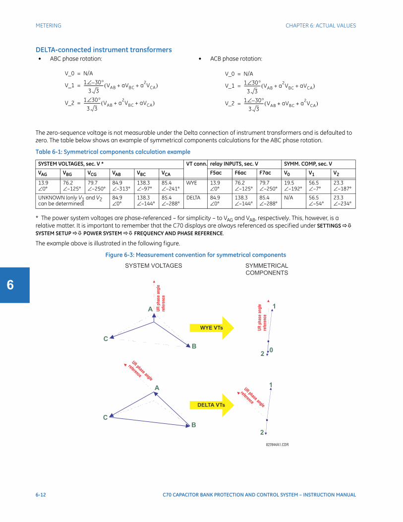
6-12 C70 CAPACITOR BANK PROTECTION AND CONTROL SYSTEM – INSTRUCTION MANUAL
METERING CHAPTER 6: ACTUAL VALUES
6
DELTA-connected instrument transformers
The zero-sequence voltage is not measurable under the Delta connection of instrument transformers and is defaulted to zero. The table below shows an example of symmetrical components calculations for the ABC phase rotation.
Table 6-1: Symmetrical components calculation example
* The power system voltages are phase-referenced – for simplicity – to VAG and VAB, respectively. This, however, is a relative matter. It is important to remember that the C70 displays are always referenced as specified under SETTINGS SYSTEM SETUP POWER SYSTEM FREQUENCY AND PHASE REFERENCE.
The example above is illustrated in the following figure.
Figure 6-3: Measurement convention for symmetrical components
• ABC phase rotation: • ACB phase rotation:
SYSTEM VOLTAGES, sec. V * VT conn. relay INPUTS, sec. V SYMM. COMP, sec. V
VAG VBG VCG VAB VBC VCA F5ac F6ac F7ac V0 V1 V2
13.9∠0°
76.2∠–125°
79.7∠–250°
84.9∠–313°
138.3∠–97°
85.4∠–241°
WYE 13.9∠0°
76.2∠–125°
79.7∠–250°
19.5∠–192°
56.5∠–7°
23.3∠–187°
UNKNOWN (only V1 and V2 can be determined)
84.9∠0°
138.3∠–144°
85.4∠–288°
DELTA 84.9∠0°
138.3∠–144°
85.4∠–288°
N/A 56.5∠–54°
23.3∠–234°
V_0 N/A=
V_1 1 30– °∠3 3
------------------ VAB aVBC a2VCA+ +( )=
V_2 1 30°∠3 3
--------------- VAB a2VBC aVCA+ +( )=
V_0 N/A=
V_1 1 30°∠3 3
--------------- VAB a2VBC aVCA+ +( )=
V_2 1 30– °∠3 3
------------------ VAB aVBC a2VCA+ +( )=
827844A1.CDR
A
B
C
WYE VTs
1
02
A
B
C
DELTA VTs
1
2
SYSTEM VOLTAGES SYMMETRICAL
COMPONENTS
UR p
hase
ang
lere
fere
nce
UR p
hase
ang
lere
fere
nce
UR phase angle
reference
UR phase angle
reference
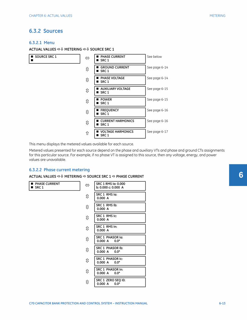
CHAPTER 6: ACTUAL VALUES METERING
C70 CAPACITOR BANK PROTECTION AND CONTROL SYSTEM – INSTRUCTION MANUAL 6-13
6
6.3.2 Sources
6.3.2.1 MenuACTUAL VALUES METERING SOURCE SRC 1
This menu displays the metered values available for each source.
Metered values presented for each source depend on the phase and auxiliary VTs and phase and ground CTs assignments for this particular source. For example, if no phase VT is assigned to this source, then any voltage, energy, and power values are unavailable.
6.3.2.2 Phase current meteringACTUAL VALUES METERING SOURCE SRC 1 PHASE CURRENT
SOURCE SRC 1 PHASE CURRENT
SRC 1See below
GROUND CURRENT SRC 1
See page 6-14
PHASE VOLTAGE SRC 1
See page 6-14
AUXILIARY VOLTAGE SRC 1
See page 6-15
POWER SRC 1
See page 6-15
FREQUENCY SRC 1
See page 6-16
CURRENT HARMONICS SRC 1
See page 6-16
VOLTAGE HARMONICS SRC 1
See page 6-17
PHASE CURRENT SRC 1 SRC 1 RMS Ia: 0.000
b: 0.000 c: 0.000 A
SRC 1 RMS Ia:0.000 A
SRC 1 RMS Ib:0.000 A
SRC 1 RMS Ic:0.000 A
SRC 1 RMS In:0.000 A
SRC 1 PHASOR Ia:0.000 A 0.0°
SRC 1 PHASOR Ib:0.000 A 0.0°
SRC 1 PHASOR Ic:0.000 A 0.0°
SRC 1 PHASOR In:0.000 A 0.0°
SRC 1 ZERO SEQ I0:0.000 A 0.0°

6-14 C70 CAPACITOR BANK PROTECTION AND CONTROL SYSTEM – INSTRUCTION MANUAL
METERING CHAPTER 6: ACTUAL VALUES
6
The metered phase current values are displayed in this menu. The "SRC 1" text gets replaced by whatever name was programmed by the user for the associated source (see SETTINGS SYSTEM SETUP SIGNAL SOURCES).
6.3.2.3 Ground current meteringACTUAL VALUES METERING SOURCE SRC 1 GROUND CURRENT
The metered ground current values are displayed in this menu. The "SRC 1" text is replaced by the name programmed by the user for the associated source (see SETTINGS SYSTEM SETUP SIGNAL SOURCES).
6.3.2.4 Phase voltage meteringACTUAL VALUES METERING SOURCE SRC 1 PHASE VOLTAGE
SRC 1 POS SEQ I1:0.000 A 0.0°
SRC 1 NEG SEQ I2:0.000 A 0.0°
GROUND CURRENT SRC 1 SRC 1 RMS Ig:
0.000 A
SRC 1 PHASOR Ig:0.000 A 0.0°
SRC 1 PHASOR Igd:0.000 A 0.0°
PHASE VOLTAGE SRC 1 SRC 1 RMS Vag:
0.00 V
SRC 1 RMS Vbg:0.00 V
SRC 1 RMS Vcg:0.00 V
SRC 1 PHASOR Vag:0.000 V 0.0°
SRC 1 PHASOR Vbg:0.000 V 0.0°
SRC 1 PHASOR Vcg:0.000 V 0.0°
SRC 1 RMS Vab:0.00 V
SRC 1 RMS Vbc:0.00 V
SRC 1 RMS Vca:0.00 V
SRC 1 PHASOR Vab:0.000 V 0.0°
SRC 1 PHASOR Vbc:0.000 V 0.0°
SRC 1 PHASOR Vca:0.000 V 0.0°
SRC 1 ZERO SEQ V0:0.000 V 0.0°
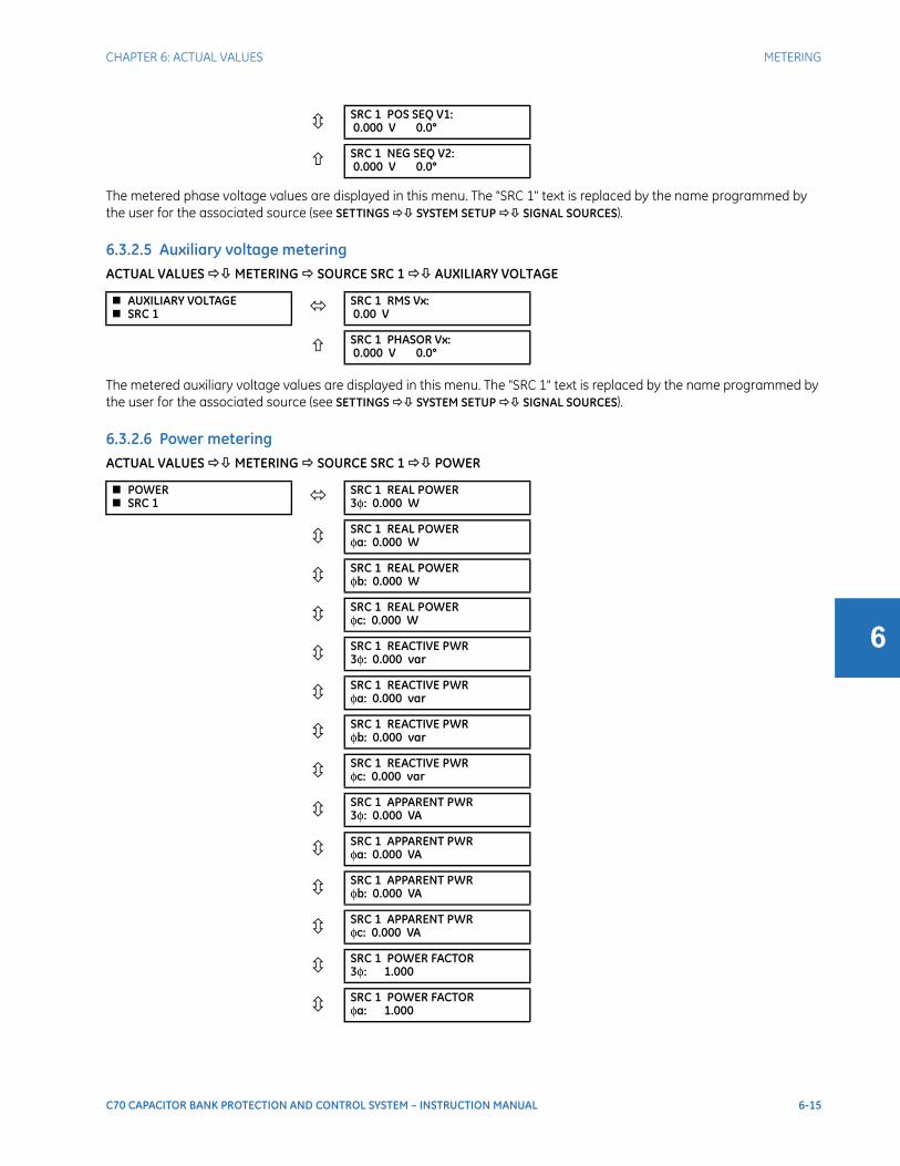
CHAPTER 6: ACTUAL VALUES METERING
C70 CAPACITOR BANK PROTECTION AND CONTROL SYSTEM – INSTRUCTION MANUAL 6-15
6
The metered phase voltage values are displayed in this menu. The "SRC 1" text is replaced by the name programmed by the user for the associated source (see SETTINGS SYSTEM SETUP SIGNAL SOURCES).
6.3.2.5 Auxiliary voltage meteringACTUAL VALUES METERING SOURCE SRC 1 AUXILIARY VOLTAGE
The metered auxiliary voltage values are displayed in this menu. The "SRC 1" text is replaced by the name programmed by the user for the associated source (see SETTINGS SYSTEM SETUP SIGNAL SOURCES).
6.3.2.6 Power meteringACTUAL VALUES METERING SOURCE SRC 1 POWER
SRC 1 POS SEQ V1:0.000 V 0.0°
SRC 1 NEG SEQ V2:0.000 V 0.0°
AUXILIARY VOLTAGE SRC 1 SRC 1 RMS Vx:
0.00 V
SRC 1 PHASOR Vx:0.000 V 0.0°
POWER SRC 1 SRC 1 REAL POWER
3φ: 0.000 W
SRC 1 REAL POWERφa: 0.000 W
SRC 1 REAL POWERφb: 0.000 W
SRC 1 REAL POWERφc: 0.000 W
SRC 1 REACTIVE PWR3φ: 0.000 var
SRC 1 REACTIVE PWRφa: 0.000 var
SRC 1 REACTIVE PWRφb: 0.000 var
SRC 1 REACTIVE PWRφc: 0.000 var
SRC 1 APPARENT PWR3φ: 0.000 VA
SRC 1 APPARENT PWRφa: 0.000 VA
SRC 1 APPARENT PWRφb: 0.000 VA
SRC 1 APPARENT PWRφc: 0.000 VA
SRC 1 POWER FACTOR3φ: 1.000
SRC 1 POWER FACTORφa: 1.000

6-16 C70 CAPACITOR BANK PROTECTION AND CONTROL SYSTEM – INSTRUCTION MANUAL
METERING CHAPTER 6: ACTUAL VALUES
6
This menu displays metered values for real, reactive, and apparent power, as well as power factor. The "SRC 1" text is replaced by the name programmed by the user for the associated source (see SETTINGS SYSTEM SETUP SIGNAL SOURCES).
When VTs are configured in wye, the C70 calculates power in each phase and three-phase power is measured as
S = VA x ÎA + VB x ÎB + VC x ÎC Eq. 6-1
When VTs are configured in delta, the C70 does not calculate power in each phase and three-phase power is measured as
S = VAB x ÎA + VCB x ÎC Eq. 6-2
where
S is the apparent power
VA, VB, VC, IA, IB, IC are phase voltage and phase current phasors
VAB and VCB are phase-to-phase voltage phasors
Î is the conjugate of I
6.3.2.7 Frequency meteringACTUAL VALUES METERING SOURCE SRC 1 FREQUENCY
The metered frequency values are displayed in this menu. The "SRC 1" text is replaced by the name programmed by the user for the associated source (see SETTINGS SYSTEM SETUP SIGNAL SOURCES).
SOURCE FREQUENCY is measured via software-implemented zero-crossing detection of an AC signal. The signal is either a Clarke transformation of three-phase voltages or currents, auxiliary voltage, or ground current as per source configuration (see the SYSTEM SETUP POWER SYSTEM settings). The signal used for frequency estimation is low-pass filtered. The final frequency measurement is passed through a validation filter that eliminates false readings due to signal distortions and transients.
6.3.2.8 Current harmonics and THD meteringACTUAL VALUES METERING SOURCE SRC 1 CURRENT HARMONICS
This menu displays metered current harmonics values. The "SRC 1" text is replaced by the name was programmed for the associated source (see SETTINGS SYSTEM SETUP SIGNAL SOURCES). Current harmonics are measured for each source for the total harmonic distortion (THD) and 2nd to 25th harmonics per phase.
SRC 1 POWER FACTORφb: 1.000
SRC 1 POWER FACTORφc: 1.000
FREQUENCY SRC 1 SRC 1 FREQUENCY:
0.00 Hz
CURRENT HARMONICS SRC 1 SRC 1 THD Ia: 0.0
Ib: 0.0 Ic: 0.0%
SRC 1 2ND Ia: 0.0Ib: 0.0 Ic: 0.0%
SRC 1 3RD Ia: 0.0Ib: 0.0 Ic: 0.0%
SRC 1 25TH Ia: 0.0Ib: 0.0 Ic: 0.0%

CHAPTER 6: ACTUAL VALUES METERING
C70 CAPACITOR BANK PROTECTION AND CONTROL SYSTEM – INSTRUCTION MANUAL 6-17
6
6.3.2.9 Voltage harmonics and THD meteringACTUAL VALUES METERING SOURCE SRC 1 VOLTAGE HARMONICS
This menu displays metered voltage harmonics values. The “SRC 1” text is replaced by the programmed name for the associated source (see the SETTINGS SYSTEM SETUP SIGNAL SOURCES menu).
To extract the 2nd to 25th voltage harmonics, each harmonic is computed on a per-phase basis, where:
N = 64 is the number of samples per cycleω0 = 2πf is the angular frequency based on the system frequency (50 or 60 Hz)k = 1, 2,..., N – 1 is the index over one cycle for the Fast Fourier Transform (FFT)m is the last sample number for the sliding windowh = 1, 2,..., 25 is the harmonic number
The short-time Fourier transform is applied to the unfiltered signal:
Eq. 6-3
The harmonics are a percentage of the fundamental signal obtained as a ratio of harmonic amplitude to fundamental amplitude multiplied by 100%. The total harmonic distortion (THD) is the ratio of the total harmonic content to the fundamental:
Eq. 6-4
6.3.3 Capacitor controlACTUAL VALUES METERING CAPACITOR CONTROL
These values indicate the time remaining before the next permissible close operation for each of the four capacitor banks.
VOLTAGE HARMONICS SRC 1 SRC 1 THD Va: 0.0
Vb: 0.0 Vc: 0.0%
SRC 1 2ND Va: 0.0Vb: 0.0 Vc: 0.0%
SRC 1 3RD Va: 0.0Vb: 0.0 Vc: 0.0%
SRC 1 25TH Va: 0.0Vb: 0.0 Vc: 0.0%
NOTE
Voltage harmonics are calculated only for Wye connected phase VTs. Ensure that the SYSTEM SETUP AC INPUTS VOLTAGE BANK F5 PHASE VT XX CONNECTION setting is “Wye” to enable voltage harmonics metering.
CAPACITOR CONTROL CAP 1 DISCHARGE TIME:
0 s
CAP 4 DISCHARGE TIME:0 s
Freal m h,( ) 2N--- f m k–( ) h ω0 t k( )⋅ ⋅( )cos⋅( )
k=
Fimag m h,( ) 2N--- f m k–( ) h ω0 t k( )⋅ ⋅( )sin⋅( )
k=
Fampl m h,( ) Freal m h,( )2 Fimag m h,( )2+=
THD F22 F3
2 … F252+ + +=
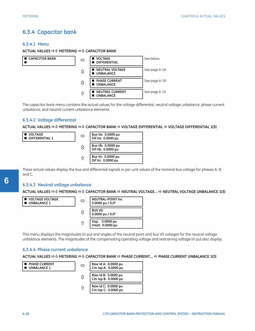
6-18 C70 CAPACITOR BANK PROTECTION AND CONTROL SYSTEM – INSTRUCTION MANUAL
METERING CHAPTER 6: ACTUAL VALUES
6
6.3.4 Capacitor bank
6.3.4.1 MenuACTUAL VALUES METERING CAPACITOR BANK
The capacitor bank menu contains the actual values for the voltage differential, neutral voltage unbalance, phase current unbalance, and neutral current unbalance elements.
6.3.4.2 Voltage differentialACTUAL VALUES METERING CAPACITOR BANK VOLTAGE DIFFERENTIAL VOLTAGE DIFFERENTIAL 1(3)
These actual values display the bus and differential signals in per-unit values of the nominal bus voltage for phases A, B, and C.
6.3.4.3 Neutral voltage unbalanceACTUAL VALUES METERING CAPACITOR BANK NEUTRAL VOLTAGE... NEUTRAL VOLTAGE UNBALANCE 1(3)
This menu displays the magnitudes (in pu) and angles of the neutral point and bus V0 voltages for the neutral voltage unbalance elements. The magnitudes of the compensating operating voltage and restraining voltage (in pu) also display.
6.3.4.4 Phase current unbalanceACTUAL VALUES METERING CAPACITOR BANK PHASE CURRENT... PHASE CURRENT UNBALANCE 1(3)
CAPACITOR BANK VOLTAGE
DIFFERENTIALSee below
NEUTRAL VOLTAGE UNBALANCE
See page 6-18
PHASE CURRENT UNBALANCE
See page 6-18
NEUTRAL CURRENT UNBALANCE
See page 6-19
VOLTAGE DIFFERENTIAL 1 Bus Va: 0.0000 pu
Dif Va: 0.0000 pu
Bus Vb: 0.0000 puDif Vb: 0.0000 pu
Bus Vc: 0.0000 puDif Vc: 0.0000 pu
VOLTAGE VOLTAGE UNBALANCE 1 NEUTRAL-POINT Vx:
0.0000 pu / 0.0°
BUS V0:0.0000 pu / 0.0°
Vop: 0.0000 puVrest: 0.0000 pu
PHASE CURRENT UNBALANCE 1 Raw Id A: 0.0000 pu
Cm Iop A: 0.0000 pu
Raw Id B: 0.0000 puCm Iop B: 0.0000 pu
Raw Id C: 0.0000 puCm Iop C: 0.0000 pu

CHAPTER 6: ACTUAL VALUES METERING
C70 CAPACITOR BANK PROTECTION AND CONTROL SYSTEM – INSTRUCTION MANUAL 6-19
6
This menu displays the magnitudes of the raw differential current and compensated operating currents (in per-units of the differential CT) for each phase.
6.3.4.5 Neutral current unbalanceACTUAL VALUES METERING CAPACITOR BANK NEUTRAL CURRENT... NEUTRAL CURRENT UNBALANCE 1(3)
This menu displays the magnitudes of the raw neutral split-phase current and compensated operating current (in per-units of the ground CT input).
6.3.5 Tracking frequencyACTUAL VALUES METERING TRACKING FREQUENCY
The tracking frequency displays here. The frequency is tracked based on the selection of the reference source with the FREQUENCY AND PHASE REFERENCE setting in the SETTINGS SYSTEM SETUP POWER SYSTEM menu. See the Power System section of chapter 5 for details.
6.3.6 FlexElementsACTUAL VALUES METERING FLEXELEMENTS FLEXELEMENT 1(16)
The operating signals for the FlexElements are displayed in pu values using the following definitions of the base units.
Table 6-2: FlexElement base units
6.3.7 RxGOOSE analogsACTUAL VALUES METERING RxGOOSE Analogs
NEUTRAL CURRENT UNBALANCE 1 Raw INsp: 0.0000 pu
Comp Iop: 0.0000 pu
TRACKING FREQUENCY TRACKING FREQUENCY
60.00 Hz
FLEXELEMENT 1 FLEXELEMENT 1
OpSig: 0.000 pu
Base unit Description
DCmA BASE = maximum value of the DCMA INPUT MAX setting for the two transducers configured under the +IN and –IN inputs.
FREQUENCY fBASE = 1 Hz
PHASE ANGLE ϕBASE = 360 degrees (see the UR angle referencing convention)
POWER FACTOR PFBASE = 1.00
RTDs BASE = 100°C
SOURCE CURRENT IBASE = maximum nominal primary RMS value of the +IN and –IN inputs
SOURCE POWER PBASE = maximum value of VBASE × IBASE for the +IN and –IN inputs
SOURCE THD & HARMONICS BASE = 1%
SOURCE VOLTAGE VBASE = maximum nominal primary RMS value of the +IN and –IN inputs
RxGOOSE Analogs RxGOOSE Analog 1
0.000
RxGOOSE Analog 320.000
6-20 C70 CAPACITOR BANK PROTECTION AND CONTROL SYSTEM – INSTRUCTION MANUAL
RECORDS CHAPTER 6: ACTUAL VALUES
6
The RxGOOSE Analog values display in this menu. The RxGOOSE Analog values are received via IEC 61850 GOOSE messages sent from other devices.
6.3.8 Transducer inputs/outputsACTUAL VALUES METERING TRANSDUCER I/O DCMA INPUTS DCMA INPUT xx
Actual values for each DCmA input channel that is enabled are displayed with the top line as the programmed channel ID and the bottom line as the value followed by the programmed units.
ACTUAL VALUES METERING TRANSDUCER I/O RTD INPUTS RTD INPUT xx
Actual values for each RTD input channel that is enabled are displayed with the top line as the programmed channel ID and the bottom line as the value.
6.4 Records
6.4.1 User-programmable fault reportsACTUAL VALUES RECORDS USER-PROGRAMMABLE FAULT REPORT
This menu displays the user-programmable fault report actual values. See the User-Programmable Fault Report section in chapter 5 for information on this feature.
6.4.2 Event recordsACTUAL VALUES RECORDS EVENT RECORDS
The C70 is provided with optional GOOSE communications capability. This feature is specified as a software option at the time of ordering. See the Order Codes section of chapter 2 for details.
DCMA INPUT xx DCMA INPUT xx
0.000 mA
RTD INPUT xx RTD INPUT xx
-50 °C
USER-PROGRAMMABLE FAULT REPORT NEWEST RECORD
NUMBER: 0
LAST CLEARED DATE:2002/8/11 14:23:57
LAST REPORT DATE:2002/10/09 08:25:27
EVENT RECORDS EVENT: XXXX
RESET OP(PUSHBUTTON)
Date and time stamps
EVENT: 3POWER ON EVENT 3
DATE: 2000/07/14
EVENT: 2POWER OFF EVENT 3
TIME: 14:53:00.03405

CHAPTER 6: ACTUAL VALUES RECORDS
C70 CAPACITOR BANK PROTECTION AND CONTROL SYSTEM – INSTRUCTION MANUAL 6-21
6
The event records menu shows the contextual data associated with up to the last 1024 events, listed in chronological order from most recent to oldest. When all 1024 event records have been filled, the oldest record is removed as a new record is added. Each event record shows the event identifier/sequence number, cause, and date/time stamp associated with the event trigger. See the COMMANDS CLEAR RECORDS menu for clearing event records.
Only major output operands generate events, not every operand. Elements that assert output per phase, for example, log operating phase output only without asserting the common three-phase operand event.
6.4.3 OscillographyACTUAL VALUES RECORDS OSCILLOGRAPHY
This menu allows the user to view the number of triggers involved and number of oscillography traces available. The cycles per record value is calculated to account for the fixed amount of data storage for oscillography. See the Oscillography section of chapter 5 for details.
A trigger can be forced here at any time by setting “Yes” to the FORCE TRIGGER? command. See the COMMANDS CLEAR RECORDS menu for information on clearing the oscillography records.
6.4.4 Data loggerACTUAL VALUES RECORDS DATA LOGGER
The OLDEST SAMPLE TIME represents the time at which the oldest available samples were taken. It is static until the log gets full, at which time it starts counting at the defined sampling rate.
The NEWEST SAMPLE TIME represents the time the most recent samples were taken. It counts up at the defined sampling rate. If the data logger channels are defined, then both values are static.
See the COMMANDS CLEAR RECORDS menu for clearing data logger records.
EVENT: 1EVENTS CLEARED
OSCILLOGRAPHY FORCE TRIGGER?
NoRange: No, Yes
NUMBER OF TRIGGERS:0
AVAILABLE RECORDS:0
CYCLES PER RECORD:0.0
LAST CLEARED DATE:2000/07/14 15:40:16
DATA LOGGER OLDEST SAMPLE TIME:
2000/01/14 13:45:51
NEWEST SAMPLE TIME:2000/01/14 15:21:19
6-22 C70 CAPACITOR BANK PROTECTION AND CONTROL SYSTEM – INSTRUCTION MANUAL
PRODUCT INFORMATION CHAPTER 6: ACTUAL VALUES
6
6.5 Product information
6.5.1 Model informationACTUAL VALUES PRODUCT INFO MODEL INFORMATION
The order code, serial number, Ethernet MAC address, date and time of manufacture, and operating time are shown here. The rear panel on the device contains similar information.
ETHERNET MAC ADDRESS — UR devices with firmware 7.0x and above have three Ethernet ports that can be used on three networks. The MAC address displays for port 1. The MAC address for port 2 is one higher. The MAC address for port 3 is one higher than port 2. In redundant mode, the MAC addresses for ports 2 and 3 are the same as port 2.
6.5.2 Firmware revisionsACTUAL VALUES PRODUCT INFO FIRMWARE REVISIONS
MODEL INFORMATION ORDER CODE LINE 1:
C70-A00-AAA-A0A-A0ARange: standard GE order code format (lines 1 to 4)
SERIAL NUMBER: Range: standard GE serial number format
ETHERNET MAC ADDRESS000000000000
Range: standard Ethernet MAC address format
MANUFACTURING DATE:0
Range: YYYY/MM/DD HH:MM:SS
OPERATING TIME:0:00:00
Range: operating time in HH:MM:SS
PMU FEATURE ACTIVE:No
Range: Yes, No
CT/ VT ADVANCED DIAGACTIVE: No
Range: Yes, No
LAST SETTING CHANGE:1970/01/01 23:11:19
Range: YYYY/MM/DD HH:MM:SS
FIRMWARE REVISIONS C70 Relay
REVISION: 7.3xRange: 0.00 to 655.35Revision number of the application firmware.
MODIFICATION FILENUMBER: 0
Range: 0 to 65535 (ID of the MOD FILE)Value is 0 for each standard firmware release.
BOOT PROGRAMREVISION: 7.01
Range: 0.00 to 655.35Revision number of the boot program firmware.
FRONT PANEL PROGRAMREVISION: 2.01
Range: 0.00 to 655.35Revision number of faceplate program firmware.
COMPILE DATE:2013/09/15 04:55:16
Range: YYYY/MM/DD HH:MM:SSDate and time when product firmware was built .
BOOT DATE:2013/09/15 16:41:32
Range: YYYY/MM/DD HH:MM:SSDate and time when the boot program was built.
FPGA PROGRAM:REVISION: 01.05
Range: 0.00 to 655.35Revision number for FPGA.
FPGA DATA:2013/09/15 16:41:32
Range: YYYY/MM/DD HH:MM:SSDate and time when the FPGA was built.

CHAPTER 6: ACTUAL VALUES PRODUCT INFORMATION
C70 CAPACITOR BANK PROTECTION AND CONTROL SYSTEM – INSTRUCTION MANUAL 6-23
6
The shown data is illustrative only. A modification file number of 0 indicates that, currently, no modifications have been installed.

6-24 C70 CAPACITOR BANK PROTECTION AND CONTROL SYSTEM – INSTRUCTION MANUAL
PRODUCT INFORMATION CHAPTER 6: ACTUAL VALUES
6
C70 CAPACITOR BANK PROTECTION AND CONTROL SYSTEM – INSTRUCTION MANUAL 7-1
C70 Capacitor Bank Protection and Control System
Chapter 7: Commands and targets
Commands and targets
This chapter outlines the Commands and Targets menus and self-tests/error messages. Commands related to the IEC 61850 protocol are outlined in the IEC 61850 section of the Settings chapter. Log/error messages for IEC 61850 are outlined in the UR Series Communications Guide.
7.1 Commands menu
The commands menu contains relay directives intended for operations personnel. All commands can be protected from unauthorized access via the command password; see the Security section of chapter 5 for details. The following flash message appears after successfully command entry.
COMMANDS
CAPACITOR BANK AUTO SETTING
COMMANDS VIRTUAL INPUTS
COMMANDS CLEAR RECORDS
COMMANDS SET DATE AND TIME
COMMANDS RELAY MAINTENANCE
COMMANDS SECURITY
COMMANDEXECUTED

7-2 C70 CAPACITOR BANK PROTECTION AND CONTROL SYSTEM – INSTRUCTION MANUAL
COMMANDS MENU CHAPTER 7: COMMANDS AND TARGETS
7
7.1.1 Capacitor bank automatic setting
7.1.1.1 Menu
The relay provides for automatic calculations of proper balancing (matching) factors of the sensitive capacitor bank protection functions. The following screens display the suggested values of the balancing factors and prompt the user to apply them. If applied from this command level, a given value is placed into the setting file and applied instantaneously in all setting groups of the relay with the same source as the active group during the auto-setting procedure.
7.1.1.2 Voltage differentialCOMMANDS CAPACITOR BANK AUTO SETTING VOLTAGE DIFFERENTIAL VOLTAGE DIFFERENITAL 1(3)
Use the automatic setting feature when the capacitor bank is online and the 87V function is enabled. For security reasons, consider applying less sensitive settings during the auto-setting process. Switching temporarily to a different setting group with less sensitive pickup thresholds is a way to provide the extra security.
The feature can be used with a manual acceptance of the auto-calculated coefficients (the VOLTAGE DIF 1 AUTO SETTING command switched to “Manual”), or with an automatic acceptance of the calculated factors (the VOLTAGE DIF 1 AUTO SETTING command switched to “Auto”).
The feature is used as follows.
Application with manual supervision of the automatically calculated factorsWhen the VOLTAGE DIF 1 AUTO SETTING command is switched to “Manual”, the auto-setting screens, one for each phase, display the values that balance best the function in a given phase and prompt for permission to apply the calculated value as a new setting. When confirmed, the auto-selected value gets applied to all setting groups configured with the same source as the active group during the auto-setting procedure.
After consent to apply the calculated coefficient is received, the "k =?.???? APPLIED" confirmation message displays for the duration of the flash message time in the second line of the screen. The time-out period is provided for the field staff to make a note of the newly applied coefficient. However, it is possible to navigate from this screen immediately. The new setting values can be viewed under the setting menu at any time.
After the process finishes, it is recommended to disable the auto-setting feature. If not disabled by the user, the feature disables itself when user-initiated front panel interface activity ceases and the C70 display dims itself.
Certain security conditions are checked during the auto-setting process. This includes deviation from the nominal frequency and verifying that the magnitudes of all three bus voltages are between 0.85 and 1.15 pu. If these conditions are violated. the SUPV FAIL message displays in the second line.
CAPACITOR BANK AUTO SETTING VOLTAGE
DIFFERENTIALSee below
NEUTRAL VOLTAGE UNBALANCE
See page 7-3
PHASE CURRENT UNBALANCE
See page 7-4
NEUTRAL CURRENT UNBALANCE
See page 7-5
VOLTAGE DIFFERENTIAL 1 VOLTAGE DIF 1 AUTO
SETTING: DisabledRange: Disabled, Manual, Auto
V DIF 1A k=####.####APPLY IN PHS A? No
Range: Yes, No
V DIF 1A k=####.####APPLY IN PHS B? No
Range: Yes, No
V DIF 1A k=####.####APPLY IN PHS C? No
Range: Yes, No

CHAPTER 7: COMMANDS AND TARGETS COMMANDS MENU
C70 CAPACITOR BANK PROTECTION AND CONTROL SYSTEM – INSTRUCTION MANUAL 7-3
7
If the voltage differential function is disabled or blocked, then the auto-setting process is not functional and the 87V NOT RUNNING message displays in the second line.
Application with automatic supervision of the automatically calculated factorsWhen the VOLTAGE DIF 1 AUTO SETTING command is switched to “Auto,” the process of calculating and applying the balancing coefficients is fully automatic. Typical applications require setting this function to “Auto” with the bank de-energized, then energizing the capacitor bank. When the bank is energized and the five-cycle timer of the 87V function expires, the balancing coefficients are calculated and automatically applied. After the new balancing factors are applied, the function switches automatically from “Auto” to “Disabled” and 87V becomes operational. In essence, when in the “Auto” mode, the user confirmation is processed immediately after the balancing values become available. The C70 does not display the applied coefficients in “Auto” mode; rather, they are be viewed in the SETTINGS menu.
If the supervisory conditions are not satisfied in the “Auto” mode within the time specified by the DEFAULT MESSAGE TIMEOUT setting, the AUTO FAIL message displays and the 87V function starts running with the pre-existing settings for the balancing factors.
The advantage of automatically calculating factors is that the bank is immediately protected after energization. However, due to energization inrush and distortion of voltages, the factors may not be accurate enough for the most sensitive stages. Therefore, it is good practice to block the most sensitive stages on energization, manually adjust the factors to reduce the differential signal, and then enable the most sensitive stages.
7.1.1.3 Neutral voltage unbalanceCOMMANDS CAPACITOR BANK AUTO SETTING NEUTRAL VOLTAGE UNBALANCE NEUTRAL VOLTAGE UNBALANCE 1(3)
Use the auto-setting feature when the capacitor bank is online and the 59NU function is enabled. For security reasons, consider applying less sensitive settings during the auto-setting process. Switching temporarily to a different setting group with less sensitive pickup thresholds is a method to provide the extra security.
This feature can be used with a manual acceptance of the auto-calculated coefficients (the NTRL VOL UNBAL 1 AUTO SET command switched to “Manual”), or with an automatic acceptance of the calculated factors (the NTRL VOL UNBAL 1 AUTO SET command switched to “Auto”).
The feature is used as follows.
Manual supervision of automatically calculated factorsWhen the NTRL VOL UNBAL 1 AUTO SET command is switched to “Manual,” the auto-setting screens (one for each of the two factors) display values that best balance the function and prompt for permission to apply the calculated value as a new setting. When confirmed, the auto-selected value is applied to all setting groups having same source as the active group during auto-setting procedure. Both ratios (XA / XB and XA / XC) must be set correctly to clear the inherent bank unbalance. After consent to apply the calculated coefficient is received via the keypad, the "k =?.???? APPLIED" confirmation message idisplays for the duration of the flash message time. The time-out period is intended for field staff to make note of the newly applied coefficient. However, it is possible to immediately navigate from this screen. The new setting values can be viewed in the SETTINGS menu at any time.
After the process finishes, it is recommended to disable the auto-setting feature. If not manually disabled, the feature automatically disables itself when user-initiated front panel interface activity ceases and the C70 display is dimmed.
Certain security conditions are checked during the auto-setting process, such as the frequency deviation from the nominal frequency and the magnitude of the positive-sequence current above 0.1 pu. If any of these conditions are violated, the SUPV FAIL message displays in the second line.
NEUTRAL VOLTAGE UNBALANCE 1 NTRL VOL UNBAL 1
AUTO SET: DisabledRange: Disabled, Manual, Auto
XA/XB RATIO k=0.0000APPLY? No
Range: Yes, No
XA/XC RATIO k=0.0000APPLY? No
Range: Yes, No
7-4 C70 CAPACITOR BANK PROTECTION AND CONTROL SYSTEM – INSTRUCTION MANUAL
COMMANDS MENU CHAPTER 7: COMMANDS AND TARGETS
7
If the neutral voltage unbalance function is disabled or blocked, the auto-setting process is not functional and the 59NU NOT RUNNING message displays in the second line.
Automatic supervision of automatically calculated factorsWhen the NTRL VOL UNBAL 1 AUTO SET command is switched to “Auto”, the process of calculating and applying the balancing coefficients is fully automatic. Typical applications require setting this function to “Auto” with the bank de-energized, then energizing the capacitor bank. After the function is set to “Auto,” it expects to read valid input signals as a result of bank energization within the display flash message time duration to calculate and apply factors; otherwise, the function is returned to “Disabled.” When the bank is energized and the five-cycle timer of the 59NU function expires, the balancing coefficients are calculated and automatically applied. When the new balancing factors are applied, the function switches automatically from “Auto” to “Disabled” and the 59NU function becomes operational. In essence, when in the “Auto” mode, the confirmation command executes automatically immediately after the balancing values are available. The C70 does not display the applied coefficients in the “Auto” mode; rather, they are be viewed in the SETTINGS menu.
When the supervisory conditions are not satisfied in “Auto” mode, the AUTO FAIL message displays and the 59NU function starts running with the pre-existing settings for the balancing factors.
7.1.1.4 Phase current unbalanceCOMMANDS CAPACITOR BANK AUTO SETTING PHASE CURRENT UNBALANCE PHASE CURRENT UNBALANCE 1(3)
Use the auto-setting feature when the capacitor bank is online and the 60P function is enabled. For security reasons, apply less sensitive settings during the auto-setting process. Switching temporarily to an alternate setting group with less sensitive pickup thresholds is a method to provide the extra security.
The feature can be used with by manual accepting the auto-calculated coefficients (the CUR UNBALACE 1 AUTO SETTINGS command switched to “Manual”) or by automatic acceptance of the calculated factors (the CUR UNBALACE 1 AUTO SETTINGS command switched to “Auto”).
The feature is used as follows.
Application with manual supervision of the automatically calculated factorsWhen the CUR UNBALACE 1 AUTO SETTINGS command is switched to “Manual,” the auto-setting screens (one for each phase) display values that best balance the function in a given phase and prompt for permission to apply the calculated value as a new setting. When confirmed, the auto-selected value is applied to all setting groups having same source as active group during the auto-setting procedure. The balancing factors can be either positive or negative, depending on which of the two banks has a lower impedance, and on the polarity of the differential CTs connected to the relay.
After user consent to apply the calculated coefficient is received, the "k =?.???? APPLIED" confirmation message displays for the duration of the flash message time. The timeout period allows field staff to make note of the newly applied coefficient. However, it is possible to immediately navigate from this screen. The new setting values can be viewed in the SETTINGS menu at any time.
After the process finishes, it is recommended to disable the auto-setting feature. If not disabled, the feature automatically disables itself when user-initiated front panel interface activity ceases and the C70 display is dimmed.
Certain security conditions are checked during the auto-setting process, such as frequency deviation from the nominal and the magnitude of the phase currents above 0.1 pu. If any of these conditions are violated, the SUPV FAIL message displays in the second line.
PHASE CURRENT UNBALANCE 1 CUR UNBALACE 1 AUTO
SETTINGS: DisabledRange: Disabled, Manual, Auto
CUR UNB 1A k=0.0000APPLY IN PHS A? No
Range: Yes, No
CUR UNB 1A k=0.0000APPLY IN PHS B? No
Range: Yes, No
CUR UNB 1A k=0.0000APPLY IN PHS C? No
Range: Yes, No

CHAPTER 7: COMMANDS AND TARGETS COMMANDS MENU
C70 CAPACITOR BANK PROTECTION AND CONTROL SYSTEM – INSTRUCTION MANUAL 7-5
7
If the phase unbalance function is disabled or blocked, the auto-setting process is not functional and the 60P NOT RUNNING message displays in the second line.
Application with automatic supervision of the automatically calculated factorsWhen the CUR UNBALACE 1 AUTO SETTINGS command is switched to “Manual,” the process of calculating and applying the balancing coefficients is fully automatic. Typical applications require setting this function to “Auto” with the bank de-energized, then subsequently energizing the capacitor bank. If the function is set to “Auto,” it expects to read valid input signals as a result of bank energization within the flash message duration time to calculate and apply factors. Otherwise, the value is switched backed to “Disabled.” When the bank is energized and the five-cycle timer of the 60P function expires, the balancing coefficients are calculated and automatically applied. After the new balancing factors are applied, the auto-setting function switches “Auto” to “Disabled” and the 60P element becomes operational. When in “Auto” mode, the automatic confirmation command executes immediately after the balancing values are available. The C70 does not display the applied coefficients in “Auto” mode; rather, they can be viewed in the SETTINGS menu.
If the supervisory conditions are not satisfied in the “Auto” mode within time defined by the DEFAULT MESSAGE TIMEOUT setting, the AUTO FAIL message displays and the 60P function starts running with the pre-existing settings for the balancing factors.
7.1.1.5 Neutral current unbalanceCOMMANDS CAPACITOR BANK AUTO SETTING NEUTRAL CURRENT UNBALANCE NEUTRAL CURRENT UNBALANCE 1(3)
Use the auto-setting feature when the capacitor bank is online and the 60N function is enabled. For security reasons, apply less sensitive settings during the auto-setting process. Temporarily switching to an alternate setting group with less sensitive pickup thresholds is a method of providing the extra security.
The feature can be used with manual acceptance of the auto-calculated coefficients (the NTRL CUR UNBALACE 1 AUTO-SET command switched to “Manual”), or with automatic acceptance of the calculated factors (the NTRL CUR UNBALACE 1 AUTO-SET command switched to “Auto”).
The feature is used as follows.
Application with manual supervision of the automatically calculated factorsWhen the NTRL CUR UNBALACE 1 AUTO-SET command is switched to “Manual,” the auto-setting screens (one for magnitude and one for angle of the compensating factor) display the values that best balance the function and prompt for permission to apply the calculated value as a new setting. When confirmed, the auto-selected value is applied to all setting groups.
After user consent to apply the calculated coefficient is received, the "k =?.???? APPLIED" confirmation message displays for the duration of the flash message time. The timeout period allows field staff to make note of the newly applied coefficient. However, it is possible to immediately navigate from this screen. The new setting values can be viewed in the SETTINGS menu at any time.
After the process finishes, it is recommended to disable the auto-setting feature. If not disabled by the user, the feature is automatically disabled when user-initiated front panel interface activity ceases and the C70 display is dimmed.
Certain security conditions are checked during the auto-setting process. If these conditions are violated, the SUPV FAIL message displays in the second line.
If the neutral voltage unbalance function is disabled or blocked, the auto-setting process is not functional and the 60N NOT RUNNING message displays in the second line.
NEUTRAL CURRENT UNBALANCE 1 NTRL CUR UNBALACE 1
AUTO-SET: DisabledRange: Disabled, Manual, Auto
NTRL CUR 1 k=0.0000APPLY MAGNITUDE? No
Range: Yes, No
NTRL CUR 1 k=0°APPLY ANGLE? No
Range: Yes, No
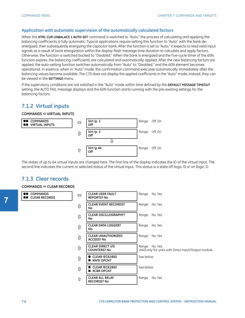
7-6 C70 CAPACITOR BANK PROTECTION AND CONTROL SYSTEM – INSTRUCTION MANUAL
COMMANDS MENU CHAPTER 7: COMMANDS AND TARGETS
7
Application with automatic supervision of the automatically calculated factorsWhen the NTRL CUR UNBALACE 1 AUTO-SET command is switched to “Auto,” the process of calculating and applying the balancing coefficients is fully automatic. Typical applications require setting this function to “Auto” with the bank de-energized, then subsequently energizing the capacitor bank. After the function is set to “Auto,” it expects to read valid input signals as a result of bank energization within the display flash message time duration to calculate and apply factors. Otherwise, the function is switched backed to “Disabled.” When the bank is energized and the five-cycle timer of the 60N function expires, the balancing coefficients are calculated and automatically applied. After the new balancing factors are applied, the auto-setting function switches automatically from “Auto” to “Disabled,” and the 60N element becomes operational. In essence, when in “Auto” mode, the confirmation command executes automatically immediately after the balancing values become available. The C70 does not display the applied coefficients in the “Auto” mode; instead, they can be viewed in the SETTINGS menu.
If the supervisory conditions are not satisfied in the “Auto” mode within time defined by the DEFAULT MESSAGE TIMEOUT setting, the AUTO FAIL message displays and the 60N function starts running with the pre-existing settings for the balancing factors.
7.1.2 Virtual inputsCOMMANDS VIRTUAL INPUTS
The states of up to 64 virtual inputs are changed here. The first line of the display indicates the ID of the virtual input. The second line indicates the current or selected status of the virtual input. This status is a state off (logic 0) or on (logic 1).
7.1.3 Clear recordsCOMMANDS CLEAR RECORDS
COMMANDS VIRTUAL INPUTS Virt Ip 1
OffRange: Off, On
Virt Ip 2Off
Range: Off, On
Virt Ip 64Off
Range: Off, On
COMMANDS CLEAR RECORDS CLEAR USER FAULT
REPORTS? NoRange: No, Yes
CLEAR EVENT RECORDS?No
Range: No, Yes
CLEAR OSCILLOGRAPHY?No
Range: No, Yes
CLEAR DATA LOGGER?No
Range: No, Yes
CLEAR UNAUTHORIZEDACCESS? No
Range: No, Yes
CLEAR DIRECT I/OCOUNTERS? No
Range: No, Yes. Valid only for units with Direct Input/Output module.
CLEAR IEC61850 XWSI OPCNT
See below
CLEAR IEC61850 XCBR OPCNT
See below
CLEAR ALL RELAYRECORDS? No
Range: No, Yes

CHAPTER 7: COMMANDS AND TARGETS COMMANDS MENU
C70 CAPACITOR BANK PROTECTION AND CONTROL SYSTEM – INSTRUCTION MANUAL 7-7
7
This menu contains commands for clearing historical data such as the event records. Data is cleared by changing a command setting to “Yes” and pressing the ENTER key. After clearing data, the command setting automatically reverts to “No.”
COMMANDS CLEAR RECORDS CLEAR IEC61850 XWSI OPCNT
COMMANDS CLEAR RECORDS CLEAR IEC61850 XCBR OPCNT
The Clear XSWI commands clear the disconnect operation counters for each phase and the three-phase counter. Similarly, the Clear XCBR commands clear the circuit breaker operation counters for each phase and the three-phase counter.
7.1.4 Set date and timeCOMMANDS SET DATE AND TIME
The date and time can be entered on the faceplate keypad. The time setting is based on the 24-hour clock. The complete date, as a minimum, must be entered to allow execution of this command. The new time and date take effect when the ENTER key is pressed.
When the relay is synchronizing to an external time source such as PTP, IRIG-B, or SNTP, the manually entered time is over-written.
The timescale of the entered time is local time, including daylight savings time where and when applicable.
7.1.5 Relay maintenanceCOMMANDS RELAY MAINTENANCE
This menu contains commands for relay maintenance purposes. Commands for the lamp test and order code are activated by changing a command setting to “Yes” and pressing the ENTER key. The command setting then automatically reverts to “No.” The service command is activated by entering a numerical code and pressing the ENTER key.
CLEAR IEC61850 XWSI OPCNT CLEAR XSWI 1
OpCnt? NoRange: No, Yes
CLEAR XSWI 24OpCnt? No
Range: No, Yes
CLEAR IEC61850 XWSI OPCNT CLEAR XCBR 1
OpCnt? NoRange: No, Yes
CLEAR XCBR 8OpCnt? No
Range: No, Yes
COMMANDS SET DATE AND TIME SET DATE AND TIME:
2000/01/14 13:47:03Range: YYYY/MM/DD HH:MM:SS
COMMANDS RELAY MAINTENANCE PERFORM LAMPTEST?
NoRange: No, Yes
UPDATE ORDER CODE?No
Range: No, Yes
REBOOT RELAY?No
Range: No, Yes
SERVICE COMMAND:0
Range: 0, 101
SAVE VOLATILE DATA?:No
Range: No, Yes
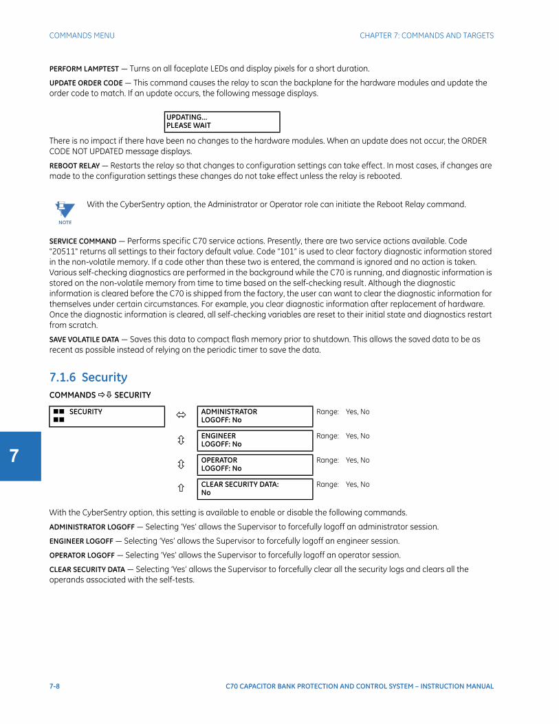
7-8 C70 CAPACITOR BANK PROTECTION AND CONTROL SYSTEM – INSTRUCTION MANUAL
COMMANDS MENU CHAPTER 7: COMMANDS AND TARGETS
7
PERFORM LAMPTEST — Turns on all faceplate LEDs and display pixels for a short duration.
UPDATE ORDER CODE — This command causes the relay to scan the backplane for the hardware modules and update the order code to match. If an update occurs, the following message displays.
There is no impact if there have been no changes to the hardware modules. When an update does not occur, the ORDER CODE NOT UPDATED message displays.
REBOOT RELAY — Restarts the relay so that changes to configuration settings can take effect. In most cases, if changes are made to the configuration settings these changes do not take effect unless the relay is rebooted.
SERVICE COMMAND — Performs specific C70 service actions. Presently, there are two service actions available. Code "20511" returns all settings to their factory default value. Code “101” is used to clear factory diagnostic information stored in the non-volatile memory. If a code other than these two is entered, the command is ignored and no action is taken. Various self-checking diagnostics are performed in the background while the C70 is running, and diagnostic information is stored on the non-volatile memory from time to time based on the self-checking result. Although the diagnostic information is cleared before the C70 is shipped from the factory, the user can want to clear the diagnostic information for themselves under certain circumstances. For example, you clear diagnostic information after replacement of hardware. Once the diagnostic information is cleared, all self-checking variables are reset to their initial state and diagnostics restart from scratch.
SAVE VOLATILE DATA — Saves this data to compact flash memory prior to shutdown. This allows the saved data to be as recent as possible instead of relying on the periodic timer to save the data.
7.1.6 SecurityCOMMANDS SECURITY
With the CyberSentry option, this setting is available to enable or disable the following commands.
ADMINISTRATOR LOGOFF — Selecting ‘Yes’ allows the Supervisor to forcefully logoff an administrator session.
ENGINEER LOGOFF — Selecting ‘Yes’ allows the Supervisor to forcefully logoff an engineer session.
OPERATOR LOGOFF — Selecting ‘Yes’ allows the Supervisor to forcefully logoff an operator session.
CLEAR SECURITY DATA — Selecting ‘Yes’ allows the Supervisor to forcefully clear all the security logs and clears all the operands associated with the self-tests.
UPDATING...PLEASE WAIT
NOTE
With the CyberSentry option, the Administrator or Operator role can initiate the Reboot Relay command.
SECURITY ADMINISTRATOR
LOGOFF: NoRange: Yes, No
ENGINEERLOGOFF: No
Range: Yes, No
OPERATORLOGOFF: No
Range: Yes, No
CLEAR SECURITY DATA:No
Range: Yes, No

CHAPTER 7: COMMANDS AND TARGETS TARGETS MENU
C70 CAPACITOR BANK PROTECTION AND CONTROL SYSTEM – INSTRUCTION MANUAL 7-9
7
7.2 Targets menu
Each C70 element with a TARGET setting has a target message that when activated by its element is displayed in sequence with any other currently active target messages in the TARGETS menu. In the example shown, the Phase TOC4 and Digital Element 48 target settings are active and so have their targets displayed. The down arrow below the two elements indicates that there can be other active elements beyond these two.
For more information, see the description of target messages in the next section, and the Introduction to Elements section in the Settings chapter for instructions on TARGET setting.
When no targets are active, the display reads NO ACTIVE TARGETS.
7.2.1 Target messagesWhen there are no active targets, the first target to become active causes the display to immediately default to that message. If there are active targets and the user is navigating through other messages, and when the default message timer times out (i.e. the keypad has not been used for a determined period of time), the display again defaults back to the target message.
The range of variables for the target messages is described below. Phase information is included if applicable. If a target message status changes, the status with the highest priority displays.
Table 7-1: Target message priority status
If a self test error is detected, a message appears indicating the cause of the error. For example UNIT NOT PROGRAMMED indicates that the minimal relay settings have not been programmed.
7.2.2 Relay self-tests
7.2.2.1 DescriptionThe relay performs a number of self-test diagnostic checks to ensure device integrity. The two types of self-tests (major and minor) are listed in the following tables. When either type of error occurs, the Trouble LED Indicator turns on and a target message displays. All errors record an event in the event recorder. Latched errors can be cleared by pressing the RESET key, providing the condition is no longer present.
Major self-test errors also result in the following:
• The critical fail relay on the power supply module de-energizes
• All other output relays de-energize and are prevented from further operation
TARGETS
PHASE TOC4OP: A B -
Displayed only if targets for this element are active. Example shown.
DIGITAL ELEMENT 48:LATCHED
Displayed only if targets for this element are active. Example shown.
Priority Active status Description
1 OP element operated and still picked up
2 PKP element picked up and timed out
3 LATCHED element had operated but has dropped out

7-10 C70 CAPACITOR BANK PROTECTION AND CONTROL SYSTEM – INSTRUCTION MANUAL
TARGETS MENU CHAPTER 7: COMMANDS AND TARGETS
7
• The faceplate In Service LED indicator turns off
• A RELAY OUT OF SERVICE event is recorded
7.2.2.2 Major self-test error messagesThe major self-test errors are outlined in this section.
• Latched target message: Yes.
• Description of problem: One or more installed hardware modules is not compatible with the C70 order code.
• How often the test is performed: Module dependent.
• What to do: Contact the factory and supply the failure code noted in the display. The “xxx” text identifies the failed module (for example, F8L).
• Latched target message: No.
• Description of problem: The configuration of modules does not match the order code stored in the C70.
• How often the test is performed: On power up. Afterwards, the backplane is checked for missing cards every five seconds.
• What to do: Check all modules against the order code, ensure they are inserted properly, and cycle control power. If the problem persists, contact the factory.
• Latched target message: No.
• Description of problem: A FlexLogic equation is incorrect.
• How often the test is performed: The test is event driven, performed whenever FlexLogic equations are modified.
• What to do: Finish all equation editing and use self tests to debug any errors.
• Latched target message: No.
• Description of problem: The PRODUCT SETUP INSTALLATION RELAY SETTINGS setting indicates the C70 is not programmed.
• How often the test is performed: On power up and whenever the PRODUCT SETUP INSTALLATION RELAY SETTINGS setting is altered.
• What to do: Program all settings and then set PRODUCT SETUP INSTALLATION RELAY SETTINGS to “Programmed.”
7.2.2.3 Minor self-test error messagesMost of the minor self-test errors can be disabled. See the settings in the User-programmable Self-tests section in chapter 5.
• Latched target message: Yes.
• Description of problem: Module hardware failure detected.
• How often the test is performed: Module dependent.
INCOMPATIBLE H/W:Contact Factory (xxx)
EQUIPMENT MISMATCH:with 2nd line detail
FLEXLOGIC ERROR:with 2nd line detail
UNIT NOT PROGRAMMED:Check Settings
MODULE FAILURE___:Contact Factory (xxx)
CHAPTER 7: COMMANDS AND TARGETS TARGETS MENU
C70 CAPACITOR BANK PROTECTION AND CONTROL SYSTEM – INSTRUCTION MANUAL 7-11
7
• What to do: Contact the factory and supply the failure code noted in the display. The “xxx” text identifies the failed module (for example, F8L).
For Module Failure 31, a new process card hardware is available. The process card hardware has been enhanced to support new features, such as fast distance protection, Synchrophasors Frequency, and Rate of Change of Frequency calculations to conform to C37.118 - 2005 standard. The new functionality leveraging the hardware is supported with firmware revision 7.25 and above. When using an older revision of the process card with a new firmware revision (7.25), Module Failure 31 indicates the limited functionality. If your application requires the new functionality, then new process card hardware is required and otherwise you can continue using the existing hardware. To know the revision of your hardware, contact the factory.
• Latched target message: Yes.
• Description of problem: The battery is not functioning.
• How often the test is performed: The battery is monitored every five seconds. The error message displays after 60 seconds if the problem persists.
• What to do: Replace the battery as outlined in the Maintenance chapter.
• Latched target message: No.
• Description of problem: Direct input and output settings are configured for a ring, but the connection is not in a ring.
• How often the test is performed: Every second.
• What to do: Check direct input and output configuration and wiring.
• Latched target message: No.
• Description of problem: The Ethernet connection has failed for the specified port.
• How often the test is performed: Every five seconds.
• What to do: Check the Ethernet port connection on the switch.
• Latched target message: No.
• Description of problem: A bad IRIG-B input signal has been detected.
• How often the test is performed: Monitored whenever an IRIG-B signal is received.
• What to do: Ensure the following:
– The IRIG-B cable is properly connected.
– Proper cable functionality (that is, check for physical damage or perform a continuity test).
– The IRIG-B receiver is functioning.
– Check the input signal level (it can be less than specification).
If none of these apply, then contact the factory.
• Latched target message: No.
• Description of problem: No PTP enabled port has good PTP signal input.
MAINTENANCE ALERT:Replace Battery
MAINTENANCE ALERT:Direct I/O Ring Break
MAINTENANCE ALERT:ENET PORT # OFFLINE
MAINTENANCE ALERT:**Bad IRIG-B Signal**
MAINTENANCE ALERT:**Bad PTP Signal**

7-12 C70 CAPACITOR BANK PROTECTION AND CONTROL SYSTEM – INSTRUCTION MANUAL
TARGETS MENU CHAPTER 7: COMMANDS AND TARGETS
7
• How often the test is performed: Activated when no acceptable signal is being received.
• What to do: Ensure the following:
– The Ethernet cable(s) are properly connected.
– At least one PTP grandmaster-capable clock is functioning.
– If strict PP is enabled, that entire network is PP compliant.
– The network is delivering PTP messages to the relay.
• Latched target message: No.
• Description of problem: An Ethernet connection has failed.
• How often the test is performed: Monitored every five seconds.
• What to do: Check Ethernet connections. Port 1 is the primary port and port 2 is the secondary port.
• Latched target message: No.
• Description of problem: The SNTP server is not responding.
• How often the test is performed: Every 10 to 60 seconds.
• What to do: Check that Ethernet cable(s) are properly connected. Check that configuration for the SNTP server corresponds to the actual server settings. Check connectivity to the server (ping the server IP address.
• Latched target message: No.
• Description of problem: A discrepancy has been detected between the actual and desired state of a latching contact output of an installed type “4L” module.
• How often the test is performed: Upon initiation of a contact output state change.
• What to do: Verify the state of the output contact and contact the factory if the problem persists.
• Latched target message: No.
• Description of problem: A data item in a configurable GOOSE data set is oscillating.
• How often the test is performed: Upon scanning of each configurable GOOSE data set.
• What to do: The “xxx” text denotes the data item that has been detected as oscillating. Evaluate all logic pertaining to this item.
• Latched target message: No.
• Description of problem: A direct device is configured but not connected.
• How often the test is performed: Every second.
• What to do: Check direct input and output configuration and wiring.
MAINTENANCE ALERT:Port ## Failure
MAINTENANCE ALERT:SNTP Failure
MAINTENANCE ALERT:4L Discrepancy
MAINTENANCE ALERT:GGIO Ind xxx oscill
DIRECT I/O FAILURE:COMM Path Incomplete
RxGOOSE FAIL:Missing messages

CHAPTER 7: COMMANDS AND TARGETS TARGETS MENU
C70 CAPACITOR BANK PROTECTION AND CONTROL SYSTEM – INSTRUCTION MANUAL 7-13
7
• Latched target message: No.
• Description of problem: One or more RxGOOSE messages are not being received.
• How often the test is performed: The self-test is activated when no message is received within the expected time interval, which is the time-to-live time in the previous message. This time can be from milliseconds to minutes.
• What to do: Check GOOSE setup.
• Latched target message: Yes.
• Description of problem: The ambient temperature is greater than the maximum operating temperature (+80°C).
• How often the test is performed: Every hour.
• What to do: Remove the C70 from service and install in a location that meets operating temperature standards.
• Latched target message: Yes.
• Description of problem: Abnormal restart from modules being removed or inserted while the C70 is powered-up, when there is an abnormal DC supply, or as a result of internal relay failure.
• How often the test is performed: Event driven.
• What to do: Contact the factory.
• Latched target message: Yes.
• Description of problem: A link loss detection on an Ethernet port. The link loss is due to unplugging the cable or the switch port being down.
• How often the test is performed:
• What to do: Check the connection.
• Latched target message: Yes.
• Description of problem: The type of SFP does not match the CPU type.T-type CPU = All ports support fiber SFPs only
• What to do: A web page "SFP Transceiver Information" is provided. This page displays the type of the SFP in it . This data is to be used with the CPU type to know the cause of the problem.
• Latched target message: No.
• Description of problem: A faulty SFP or unplugging the SFP would generate this self test.
TEMP MONITOR:OVER TEMPERATURE
UNEXPECTED RESTART:Press “RESET” key
FIRST ETHERNET FAIL
SECOND ETHERNET FAIL
THIRD ETHERNET FAIL
WRONG TRANSCEIVER
SFP MODULE x FAIL
7-14 C70 CAPACITOR BANK PROTECTION AND CONTROL SYSTEM – INSTRUCTION MANUAL
TARGETS MENU CHAPTER 7: COMMANDS AND TARGETS
7
What to do: The web page "SFP Transceiver Information" described in the previous section applies for this self test as well. The "SFP Module Fail" has higher priority and it suppresses the "Ethernet Fail" target message. The "SFP MODULE FAIL FUNCTION" setting enables/disables this self test. The target for this self test is priority-based, with the third one being the highest priority. For example, if all three SFP modules fail, then the third SFP target is activated. If the third SFP module failure resolves, then the second SFP target is activated.
7.2.2.4 HardFiber self-test error messagesIn addition to those provided by the standard UR-series devices, the UR devices implement HardFiber self-tests. These are listed here. Any abnormal diagnostic condition indicated by the LEDs or the critical failure relay also results in a self-test message, so troubleshooting is described here. For other relays, such at the B95Plus, see that product’s instruction manual.
Equipment mismatch major self-test• Description of problem: The number or type of installed hardware modules does not match the order code stored in
the CPU. The standard UR-series Equipment Mismatch self-test is extended to cover the possible presence of a Process Card.
• Severity: Protection is not available and all contact outputs and shared outputs are de-asserted.
• What to do: Check all modules against the order code. Ensure they are inserted properly, and cycle the control power. If a module has intentionally been added or removed use the Update Order Code command to notify the relay that the current module configuration is correct.
Module failure major self-test• Description of problem: UR-series device module hardware failure detected.
• Severity: Protection is not available and all contact outputs and shared outputs are de-asserted.
• What to do: Contact the factory and supply the failure code noted in the display. Text in the message identifies the failed module (for example, H81). If operated on a Process Card failure, the Module Fail self-test seals-in (latches) till the UR-series device is restarted.
Process bus failure major self-test• Description of problem: Mission critical data is not available via the process bus. An AC quantity is considered critical if
both AC bank origins and the crosschecking settings are other than none. This self-test is also initiated by an AC input discrepancy being detected. See the description of the crosschecking setting in this manual for further information. In addition, this self-test can be initiated by user logic responding to loss of critical contact input/output or other data using the Process Bus Failure Operand user-programmable self-test setting. This setting is located in the Settings > Product Setup > User-Programmable Self Test menu.
• Severity: Protection is not available and all contact outputs and shared outputs are de-asserted.
• What to do: First rectify any Process Bus Trouble and Brick Trouble self-test errors. Check the actual value of the operand referenced by the Process Bus Failure Operand setting, and if “On,” determine the cause and rectify.
If the problem persists with the foregoing all clear, the cause must be an AC input discrepancy, which is typically the result of problems in the input signals to the Bricks, or faults in the Brick input conditioning hardware. If the error was annunciated the first time significant signal was encountered, suspect the former cause and check the copper connections external to the Brick. Where multiple UR-series devices have self-test errors, look for common causes.
To further isolate AC input discrepancy errors, put the relay in test-isolated mode, then one by one, temporally change an AC bank crosschecking setting to none, until the Process Bus Failure clears. Once the problem AC bank has been identified, the values from each of the two Bricks can be examined individually by temporarily mapping each to an AC bank with a single origin.
Process bus trouble minor self-test• Description of problem: Communications problems with one or more Bricks. The text of the message identifies the
affected field units. This self-test is initiated by low received signal levels at either the Brick or Process Card end, and by the sustained failure to receive poll responses from the proper Brick.
CHAPTER 7: COMMANDS AND TARGETS TARGETS MENU
C70 CAPACITOR BANK PROTECTION AND CONTROL SYSTEM – INSTRUCTION MANUAL 7-15
7
• Severity: This self-test error does not directly inhibit protection. However, the affected Brick inputs/outputs may not be available to the UR-series device.
• What to do: Check the field unit actual values. An indication of equipment mismatch means that messages are being received from a Brick, but there is a discrepancy between the settings and the actual Brick serial number, order code, and/or core number. Check that the correct core on the correct Brick is patched through to the correct Process Card port, and that the field unit settings are correct. An indication of communications loss means that no messages are being received. Check that the patching is correct, and that the Brick has power. If that is not the problem, use a professional optical fiber connector cleaning kit to clean both sides of all optical fiber connections from the Process Card through to the affected Brick. If the problem continues after cleaning, consult the factory.
Brick trouble minor self-test• Description of problem: Brick internal self-testing has detected a trouble internal to the Brick.
• Severity: This self-test error does not directly inhibit protection. However, some or all of the affected Brick inputs/outputs may not be available to the UR-series device.
• What to do: Check the Brick environment for over/under temperatures and the voltage of its power source. If the ambient temperature and supply voltage are within Brick specifications, consult the factory. Troubles resulting from a Brick output failing to respond to an output command can only be detected while the command is active, and so in this case the target is latched. A latched target can be unlatched by pressing the faceplate reset key if the command has ended, however the output can still be non-functional.

7-16 C70 CAPACITOR BANK PROTECTION AND CONTROL SYSTEM – INSTRUCTION MANUAL
TARGETS MENU CHAPTER 7: COMMANDS AND TARGETS
7
C70 CAPACITOR BANK PROTECTION AND CONTROL SYSTEM – INSTRUCTION MANUAL 8-1
C70 Capacitor Bank Protection and Control System
Chapter 8: Application of settings
Application of settings
This chapter provides example(s) of use.
8.1 Arrangement of shunt capacitor banks
8.1.1 OverviewThe appropriate protection is dependent on the capacitor bank type, configuration, CTs and VTs location and connections. IEEE Standard C37.99-2000: Guide for Protection of Shunt Capacitor Banks specifies methods used for protecting different types of banks.
There are four types of arrangements and individual capacitors connections used to form a capacitor bank.
• Externally fused capacitors
• Internally fused capacitors
• Fuseless capacitors
• Unfused capacitors
These arrangements are described in the following sections.
8.1.2 Externally fused capacitorsAn individual fuse, externally mounted between the capacitor unit and the capacitor bank fuse bus, protects each capacitor unit. The capacitor unit can be designed for a relatively high voltage since the external fuse is capable of interrupting a high-voltage fault. However, the kvar rating of the individual capacitor unit is usually smaller because a minimum number of parallel units are required to limit the voltage rise on remaining units and thus allow the bank to remain in service with a capacitor can out of service. A capacitor bank using fused capacitors is configured using one or more series groups of parallel-connected capacitor units per-phase, as shown.
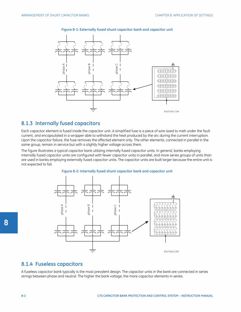
8-2 C70 CAPACITOR BANK PROTECTION AND CONTROL SYSTEM – INSTRUCTION MANUAL
ARRANGEMENT OF SHUNT CAPACITOR BANKS CHAPTER 8: APPLICATION OF SETTINGS
8
Figure 8-1: Externally fused shunt capacitor bank and capacitor unit
8.1.3 Internally fused capacitorsEach capacitor element is fused inside the capacitor unit. A simplified fuse is a piece of wire sized to melt under the fault current, and encapsulated in a wrapper able to withstand the heat produced by the arc during the current interruption. Upon the capacitor failure, the fuse removes the affected element only. The other elements, connected in parallel in the same group, remain in service but with a slightly higher voltage across them.
The figure illustrates a typical capacitor bank utilizing internally fused capacitor units. In general, banks employing internally fused capacitor units are configured with fewer capacitor units in parallel, and more series groups of units than are used in banks employing externally fused capacitor units. The capacitor units are built larger because the entire unit is not expected to fail.
Figure 8-2: Internally fused shunt capacitor bank and capacitor unit
8.1.4 Fuseless capacitorsA fuseless capacitor bank typically is the most prevalent design. The capacitor units in the bank are connected in series strings between phase and neutral. The higher the bank voltage, the more capacitor elements in series.
ph
ase
A
ph
ase
B
ph
ase
C
834753A1.CDR
ph
ase
A
ph
ase
B
ph
ase
C
834754A1.CDR

CHAPTER 8: APPLICATION OF SETTINGS CONNECTIONS OF SHUNT CAPACITOR BANKS
C70 CAPACITOR BANK PROTECTION AND CONTROL SYSTEM – INSTRUCTION MANUAL 8-3
8
The expected failure of the capacitor unit element is a short circuit, where the remaining capacitor elements absorb the additional voltage. For example, if there are six capacitor units in series and each unit has eight element groups in series, then there is a total of 48 element groups in the string. If one capacitor element fails, this element is shorted and the voltage across the remaining elements is 48 / 47 of the previous value, or about 2% higher. The capacitor bank remains in service; however, successive failures of elements aggravate the problem and eventually lead to the removal of the bank.
The fuseless design is usually applied for applications at or above 34.5 kV where each string has more than 10 elements in series to ensure the remaining elements do not exceed 110% rating if an element in the string shorts.
Figure 8-3: Fuseless shunt capacitor bank and series string
8.1.5 Unfused capacitorsContrary to the fuseless configuration, where the units are connected in series, the unfused shunt capacitor bank uses a series or parallel connection of capacitor units. The unfused approach is normally used on banks below 34.5 kV, where series strings of capacitor units are not practical, or on higher voltage banks with modest parallel energy. This design does not require as many capacitor units in parallel as an externally fused bank.
8.2 Connections of shunt capacitor banks
8.2.1 Grounded wye-connected banksGrounded wye capacitor banks are a series and parallel-connected capacitor units per-phase and provide a low impedance path to ground. This offers some protection from surge overvoltages and transient overcurrents.
When a capacitor bank becomes too large, making the parallel energy of a series group too high for the capacitor units or fuses (greater than 4650 kvar), the bank can be split into two wye sections. The characteristics of the grounded double wye are similar to a grounded single wye bank. Connect the two neutrals directly with a single path to ground.
The double-wye design facilitates better protection methods. Even with inherent unbalances, the two banks respond similarly to system events, and therefore, methods based on comparing one split-phase versus the other are more sensitive and less prone to system events (phase current balance technique, for example).
8.2.2 Ungrounded wye-connected banksUngrounded wye banks do not permit zero sequence currents, third harmonic currents, or large capacitor discharge currents during system ground faults (phase-to-phase faults can still occur and results in large discharge currents). Another advantage is that overvoltages appearing at the CT secondaries are not as high as in the case of grounded banks. However, the neutral should be insulated for full line voltage because it is momentarily at phase potential when the bank is switched or when one capacitor unit fails in a bank configured with a single group of units.
834755A1.CDR
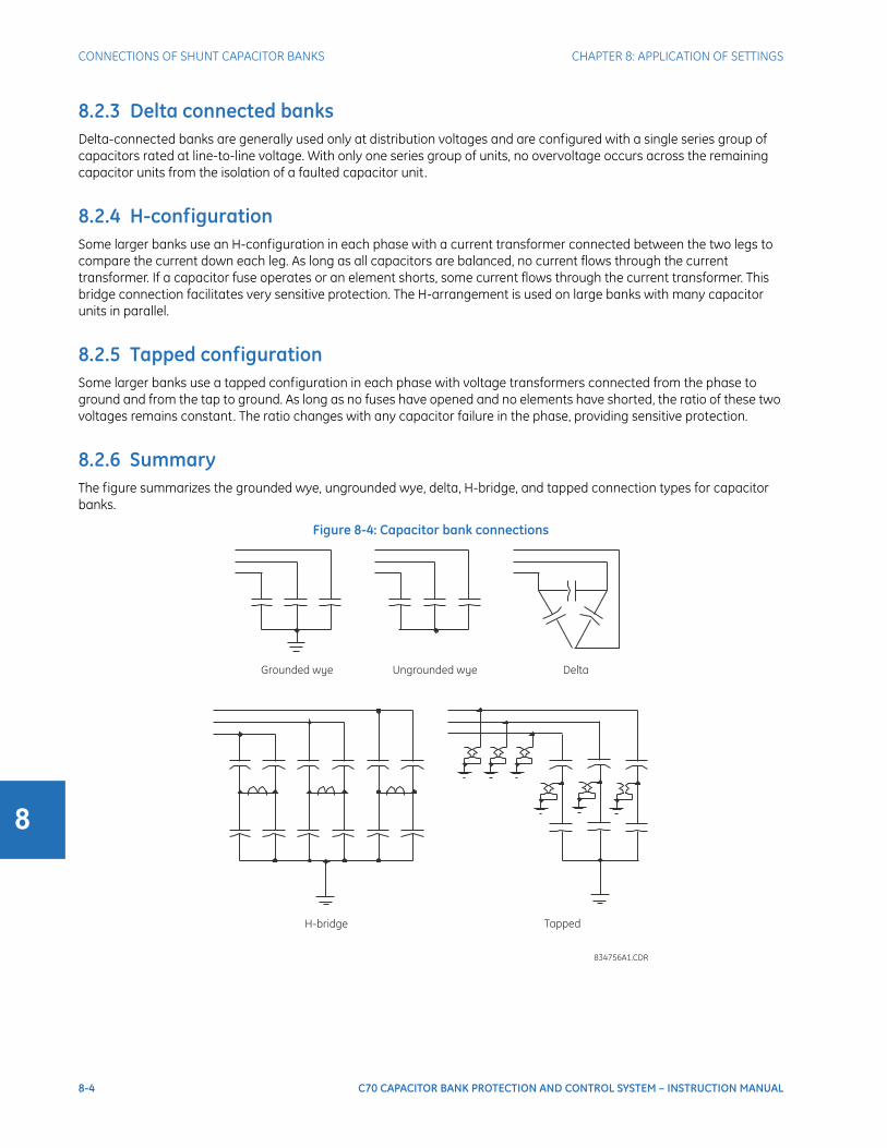
8-4 C70 CAPACITOR BANK PROTECTION AND CONTROL SYSTEM – INSTRUCTION MANUAL
CONNECTIONS OF SHUNT CAPACITOR BANKS CHAPTER 8: APPLICATION OF SETTINGS
8
8.2.3 Delta connected banksDelta-connected banks are generally used only at distribution voltages and are configured with a single series group of capacitors rated at line-to-line voltage. With only one series group of units, no overvoltage occurs across the remaining capacitor units from the isolation of a faulted capacitor unit.
8.2.4 H-configurationSome larger banks use an H-configuration in each phase with a current transformer connected between the two legs to compare the current down each leg. As long as all capacitors are balanced, no current flows through the current transformer. If a capacitor fuse operates or an element shorts, some current flows through the current transformer. This bridge connection facilitates very sensitive protection. The H-arrangement is used on large banks with many capacitor units in parallel.
8.2.5 Tapped configurationSome larger banks use a tapped configuration in each phase with voltage transformers connected from the phase to ground and from the tap to ground. As long as no fuses have opened and no elements have shorted, the ratio of these two voltages remains constant. The ratio changes with any capacitor failure in the phase, providing sensitive protection.
8.2.6 SummaryThe figure summarizes the grounded wye, ungrounded wye, delta, H-bridge, and tapped connection types for capacitor banks.
Figure 8-4: Capacitor bank connections
Grounded wye Ungrounded wye Delta
H-bridge Tapped
834756A1.CDR

CHAPTER 8: APPLICATION OF SETTINGS PROTECTION METHODS FOR CAPACITOR BANKS
C70 CAPACITOR BANK PROTECTION AND CONTROL SYSTEM – INSTRUCTION MANUAL 8-5
8
8.3 Protection methods for capacitor banks
8.3.1 OverviewThe protection of shunt capacitor banks involves both bank and system protection schemes.
Bank protection schemes are provided for faults within the capacitor bank itself. Bank protection include items such as a means to disconnect a faulted capacitor unit or capacitor elements, a means to initiate a shutdown of the bank in case of faults that can lead to a catastrophic failure, and alarms to indicate unbalance within the bank.
System protection schemes are provided to protect the capacitor bank from stresses caused by the system and to protect the substation and system from stresses that can be caused by the operation of the capacitor bank. System protection includes items such as a means to limit overvoltage and excessive transient overcurrents, and to disconnect the bank in the event of a major fault within the capacitor installation. System protection can also include alarms and methods to disconnect the entire shunt capacitor bank to prevent further damage to the capacitors due to abnormal system conditions.
In externally fused capacitor banks, several capacitor element breakdowns can occur before the fuse removes the entire unit. The external fuse operates when a capacitor unit becomes (essentially) short circuited, isolating the faulted unit. Unbalance protection removes the bank from service when the resulting overvoltage becomes excessive on the remaining healthy capacitor units.
Internally fused capacitors have individual capacitor elements within a capacitor unit that are disconnected when an element breakdown occurs. The risk of successive faults is minimized because the fuse isolates the faulty element within a few cycles. Unbalance protection removes the bank from service when the resulting unbalanced voltage becomes excessive on the remaining healthy capacitor elements or units.
For fuseless or unfused capacitor banks, a failed element is short-circuited by the weld that naturally occurs at the point of failure. Unbalance protection removes the bank from service when the resulting voltage becomes excessive on the remaining healthy capacitor elements or units.
8.3.2 Capacitor unbalance protection
8.3.2.1 ConnectionsUnbalance protection utilizes the unbalance that occurs in a normally balanced capacitor bank to detect an abnormality and initiate appropriate action. The most important function is to promptly remove the bank from service for any fault that can result in further damage. Capacitor unbalance protection is provided in many ways, depending on the capacitor bank arrangement.
A variety of unbalance protection schemes can be applied with the C70 for internally fused, externally fused, fuseless, or unfused shunt capacitor banks, as shown in the rest of this section.
The following figure illustrates a single capacitor bank, ungrounded, with no tap available. In this case, a single CT/VT module is required.

8-6 C70 CAPACITOR BANK PROTECTION AND CONTROL SYSTEM – INSTRUCTION MANUAL
PROTECTION METHODS FOR CAPACITOR BANKS CHAPTER 8: APPLICATION OF SETTINGS
8
Figure 8-5: Single bank, ungrounded, no tap available
The following figure illustrates a single capacitor bank, ungrounded, with a tap. In this case, two CT/VT modules are required.
Figure 8-6: Single bank, ungrounded, with a tap
F1
-3
F5
-7
F8
50P 51P
59B 59NU
51N
C70 CAPACITOR BANK RELAY
F4
sp
are
s
834757A1.CDR
F1
-3
F5
-7
F8
50P 51P
59B 59NU
51N
C70 CAPACITOR BANK RELAY
L5
-7
87V
F4
L4
L1
-3
sp
are
s
834758A1.CDR

CHAPTER 8: APPLICATION OF SETTINGS PROTECTION METHODS FOR CAPACITOR BANKS
C70 CAPACITOR BANK PROTECTION AND CONTROL SYSTEM – INSTRUCTION MANUAL 8-7
8
Figure 8-7: Single bank, grounded, with a tap
The following figure illustrates parallel capacitor banks, ungrounded, no tap available, and with current unbalance protection. In this case, two CT/VT modules are required.
Figure 8-8: Parallel banks, ungrounded, no tap available, current unbalance protection
The following figure illustrates parallel capacitor banks, grounded, no tap available, and with current unbalance protection. In this case, two CT/VT modules are required.
F1
-3
F5
-7
50P 51P
59B
51N
C70 CAPACITOR BANK RELAY
L5
-7
87V
F4
L4
L1
-3
L8
sp
are
s
834759A1.CDR
F1
-3
F5
-7
F8
50P 51P
59B 59NU
51N
C70 CAPACITOR BANK RELAY
L4
L1
-3
60P
(A)
60P
(B)
60P
(C)
60N
F4
L5
-7
L8
sp
are
s
834760A1.CDR
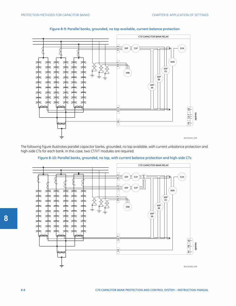
8-8 C70 CAPACITOR BANK PROTECTION AND CONTROL SYSTEM – INSTRUCTION MANUAL
PROTECTION METHODS FOR CAPACITOR BANKS CHAPTER 8: APPLICATION OF SETTINGS
8
Figure 8-9: Parallel banks, grounded, no tap available, current balance protection
The following figure illustrates parallel capacitor banks, grounded, no tap available, with current unbalance protection and high-side CTs for each bank. In this case, two CT/VT modules are required.
Figure 8-10: Parallel banks, grounded, no tap, with current balance protection and high-side CTs
F1
-3
F5
-7
50P 51P
59B
51N
C70 CAPACITOR BANK RELAY
L4
L1
-3
60P
(A)
60P
(B)
60P
(C)
60N
F4
L5
-7
L8
sp
are
s
834761A1.CDR
F1
-3
F5
-7
50P 51P
59B
51N
C70 CAPACITOR BANK RELAY
L4
L5
-7
60P
(A)
60P
(B)
60P
(C)
60N
L1
-3
50P 51PF
4F
8L
8
sp
are
s
834762A1.CDR

CHAPTER 8: APPLICATION OF SETTINGS PROTECTION METHODS FOR CAPACITOR BANKS
C70 CAPACITOR BANK PROTECTION AND CONTROL SYSTEM – INSTRUCTION MANUAL 8-9
8
The following figure illustrates parallel capacitor banks, grounded, with taps and current unbalance protection. In this case, three CT/VT modules are required.
Figure 8-11: Parallel banks, grounded, with taps and current unbalance protection
The normal functions of unbalance relaying are as follows:
• Trip the bank promptly if an unbalance indicates the possible presence of external arcing or a cascading fault within the capacitor bank
• Provide early unbalance alarm signal(s) to indicate the operation of fuses (internally or externally fused capacitors) or failure of capacitor elements (fuseless or unfused capacitors)
• Trip the bank for unbalances that are large enough to indicate that continuing operation can result in the following:
– Damage to remaining good capacitor units or elements from overvoltage
– Fuse malfunction
– Inappropriate filter operation (for capacitor banks that are a part of a harmonic filter)
– Other undesirable consequences
Note that there can be undetectable failure modes for each type of unbalance protection. These need to be backed up by other types of protection.
8.3.2.2 Unbalance trip element considerationsNote the following points when using the unbalance trip element.
• Minimize the unbalance trip element time delay to reduce damage from an arcing fault within the bank structure and prevent exposure of the remaining capacitor units to overvoltage conditions beyond their permissible limits. For a single-phase or an open-phase condition, keep the time delay short enough to avoid damage to the current transformer or voltage transformer and to the relay system.
• Have enough time delay on the unbalance trip element to avoid false operations due to inrush, system ground faults, switching of nearby equipment, and non-simultaneous pole operation of the energizing switch. For most applications, 0.1 seconds is adequate. For unbalance relaying systems that operate on a system voltage unbalance (ground fault), a delay slightly longer than the upstream protection fault clearing time is required to avoid tripping due to a system fault. Longer delays increase the probability of catastrophic bank failure.
F1
-3
F5
-7
50P 51P
59B
51N
C70 CAPACITOR BANK RELAY
L4
L1
-3
60P
(A)
60P
(B)
60P
(C)
60N
S1
-3
,5-7
87V
87V
F4
L5
-7
L8
S4
S8
sp
are
s
834763A1.CDR

8-10 C70 CAPACITOR BANK PROTECTION AND CONTROL SYSTEM – INSTRUCTION MANUAL
PROTECTION METHODS FOR CAPACITOR BANKS CHAPTER 8: APPLICATION OF SETTINGS
8
• With grounded capacitor banks, the failure of one pole of the switching device or the single phasing from a blown bank fuse allows zero sequence currents to flow in system ground relays. Coordinate capacitor bank relaying, including the operating time of the switching device, with the operation of the system ground relays to avoid tripping system load.
• The unbalance trip element can need to be delayed to account for the settling time of the protection system on initial energization and for the transient response of certain capacitor voltage transformers, and so on, which can be a part of the unbalance protection system
• The unbalance trip scheme can include a lockout feature to prevent inadvertent closing of the capacitor bank switching device if an unbalance trip has occurred
• To allow for the effects of inherent unbalance, set the unbalance element trip to operate at a signal level halfway between the critical step and the next lower step. The critical step is the number of fuse operations or shorted elements that cause an overvoltage on healthy capacitor units in excess of 110% of the capacitor unit rated voltage or the capacitor unit manufacturer's recommended maximum continuous operating voltage. In addition, for internally fused capacitor units, the critical step can be the number of internal fuse operations at which tripping should occur as recommended by the capacitor manufacturer.
• If switch failure or single phasing due to a blown main fuse can result in the continuous voltage exceeding the relay or VT rating, configure additional elements in the relay to trip the bank for this condition
• The unbalance element detects only the unbalance in the capacitor bank and in supply voltage and does not respond to capacitor overvoltage due to a balanced system voltage above nominal. Configure the bank phase overvoltage to trip the bank for this condition.
• Use the maximum system operating voltage, with capacitor bank energized, for setting unbalance relays
8.3.2.3 Unbalance alarm element considerationsTo allow for the effects of inherent unbalance within the bank, set the unbalance relay alarm to operate at about one-half the level of the unbalance signal determined by the calculated alarm condition based on an idealized bank. Set the alarm with sufficient time delay to override external disturbances.
8.3.3 Protection for rack faults (arc-over within capacitor banks)The most effective protection for an arc-over within the capacitor bank is provided by a fast unbalance element. A short time delay for the unbalance elements minimizes the damage caused by rack faults. Intentional delays as short as 0.05 seconds have been used. This short unbalance time delay, however, should not be less than the maximum clearing time of the capacitor-unit or element fuse. Although the unbalance trip element is the most effective protection for arc detection of a series section, do not rely on the neutral voltage type of unbalance element for rack fault protection on capacitor banks where all three phases are not well separated.
Negative sequence elements can be used for inter-phase fault detection as they can be set to be more sensitive than phase overcurrent relays, but tripping should be delayed to coordinate with the other relays in the system. A setting of 10% of the rated capacitor current, taking into consideration the maximum system voltage unbalance and the maximum capacitance variation together with a time delay setting of 15 to 25 cycles, can provide adequate coordination for faults external to the bank. However, it may not prevent damage due to arcing faults within the bank structure.
8.3.4 OvervoltageThe capacitor bank and other equipment in the vicinity can be subject to overvoltages resulting from abnormal system operating conditions. If the system voltage exceeds the capacitor or equipment capability with the capacitor bank on line, remove the bank with minimum time delay. Removing the capacitor bank from the system lowers the system voltage in the vicinity of the capacitor, reducing the overvoltage on other system elements.
Especially for very large EHV capacitor banks, it is advisable to install three-phase overvoltage protection (ANSI 59B) to trip the bank quickly for extreme overvoltage conditions. To avoid nuisance tripping during transient overvoltage conditions, in some cases, tripping is delayed by a timer. The C70 provides inverse time overvoltage characteristics required to decrease tripping time for large overvoltages.
Because this tripping is not due to a fault within the capacitor bank, the capacitor bank is not locked out.
CHAPTER 8: APPLICATION OF SETTINGS SETTINGS EXAMPLE
C70 CAPACITOR BANK PROTECTION AND CONTROL SYSTEM – INSTRUCTION MANUAL 8-11
8
8.3.5 OvercurrentPhase and neutral time overcurrent elements can be applied with normal settings without encountering false operations due to inrush currents. The desirable minimum pickup is 135% of nominal phase current for grounded wye banks or 125% for ungrounded banks. Set the instantaneous elements (if used) high to override inrush or outrush transients.
For effectively grounded systems with grounded wye capacitor banks, the high-frequency outrush current into an external ground fault does not normally operate the 51N ground element. The unbalanced capacitor bank load current caused by an external ground fault can be sufficient to cause the element to pick up and trip the capacitor bank if the 51N is set too low. To prevent this inadvertent tripping, the trip of the 51N element is normally set above the capacitor phase current.
8.3.6 Loss of bus voltageIn some cases, it is necessary to trip a shunt capacitor bank if the supply bus voltage is lost. Two conditions that need to be considered are:
• Re-energizing a bank with a trapped charge
• Energizing a capacitor bank without parallel load through a previously unenergized transformer
The undervoltage element (ANSI device 27B) detects loss of system voltage and trip the capacitor bank after a time delay. This delay prevents tripping of the bank for system faults external to the bank. Set the undervoltage element so that the element does not operate for voltages that require the capacitor bank to remain in service. Because this tripping is also not due to a fault within the capacitor bank (like system overvoltage tripping), the bank is not locked out.
8.4 Settings example
8.4.1 OverviewConsider protection of a capacitor bank with the following characteristics:
• VLL = 138 kV fuseless
• QB = 21 Mvar
• Two parallel strings (S = 2) in each phase with N = 7 capacitor units rated QC = 500 kvar, VC = 11.62 kV
• Each capacitor unit consisting of n = 6 series capacitors
The figure shows details. Phase capacitors are connected to ground through a neutral capacitor rated QCN = 167 kvar, VCN = 0.825 kV.
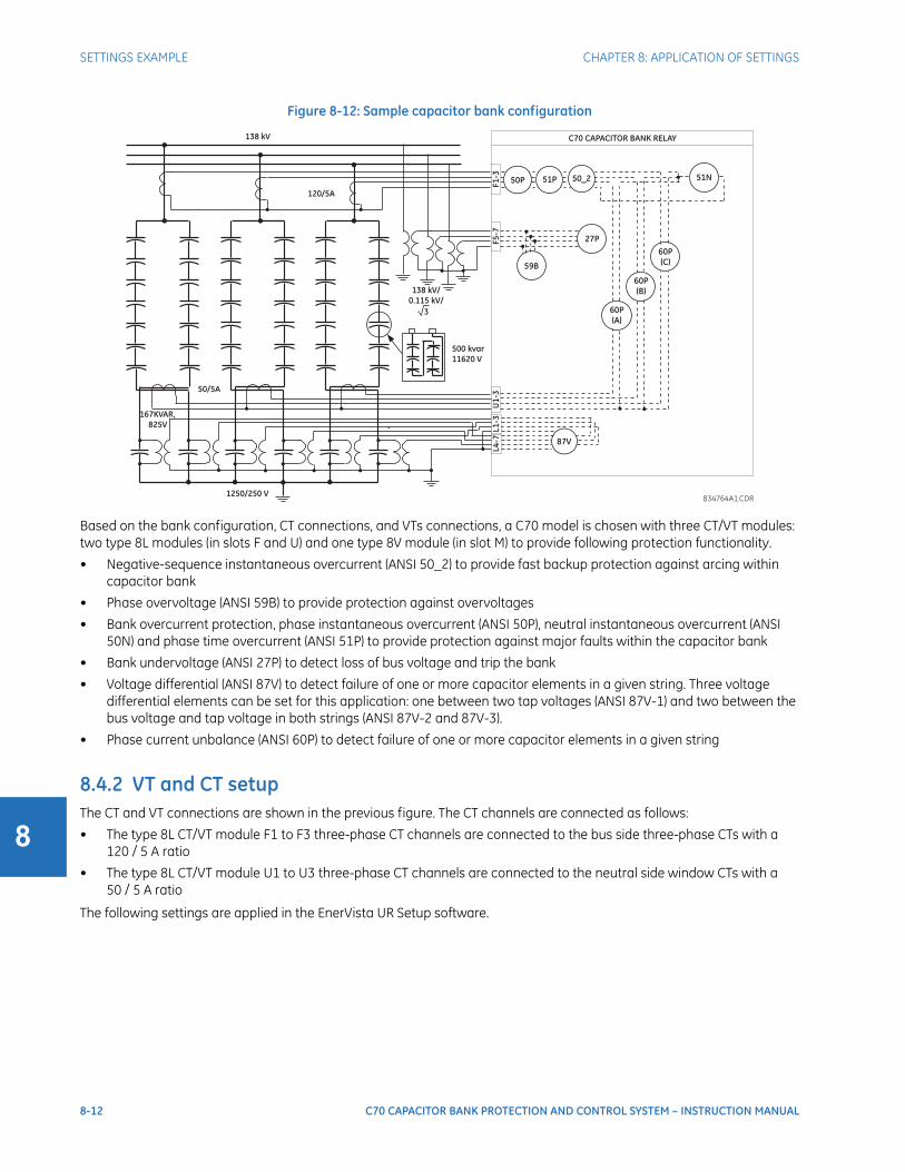
8-12 C70 CAPACITOR BANK PROTECTION AND CONTROL SYSTEM – INSTRUCTION MANUAL
SETTINGS EXAMPLE CHAPTER 8: APPLICATION OF SETTINGS
8
Figure 8-12: Sample capacitor bank configuration
Based on the bank configuration, CT connections, and VTs connections, a C70 model is chosen with three CT/VT modules: two type 8L modules (in slots F and U) and one type 8V module (in slot M) to provide following protection functionality.
• Negative-sequence instantaneous overcurrent (ANSI 50_2) to provide fast backup protection against arcing within capacitor bank
• Phase overvoltage (ANSI 59B) to provide protection against overvoltages
• Bank overcurrent protection, phase instantaneous overcurrent (ANSI 50P), neutral instantaneous overcurrent (ANSI 50N) and phase time overcurrent (ANSI 51P) to provide protection against major faults within the capacitor bank
• Bank undervoltage (ANSI 27P) to detect loss of bus voltage and trip the bank
• Voltage differential (ANSI 87V) to detect failure of one or more capacitor elements in a given string. Three voltage differential elements can be set for this application: one between two tap voltages (ANSI 87V-1) and two between the bus voltage and tap voltage in both strings (ANSI 87V-2 and 87V-3).
• Phase current unbalance (ANSI 60P) to detect failure of one or more capacitor elements in a given string
8.4.2 VT and CT setupThe CT and VT connections are shown in the previous figure. The CT channels are connected as follows:
• The type 8L CT/VT module F1 to F3 three-phase CT channels are connected to the bus side three-phase CTs with a 120 / 5 A ratio
• The type 8L CT/VT module U1 to U3 three-phase CT channels are connected to the neutral side window CTs with a 50 / 5 A ratio
The following settings are applied in the EnerVista UR Setup software.
F1
-3
F5
-7
59B
87V
51N
C70 CAPACITOR BANK RELAY
U1
-3
60P
(A)
60P
(B)
60P
(C)
138 kV
138 kV/
0.115 kV/
500 kvar
11620 V
120/5A
50/5A
50_250P 51P
27P
1250/250 V
167KVAR,
825V`
L4
-7
L1
-3
3
834764A1.CDR
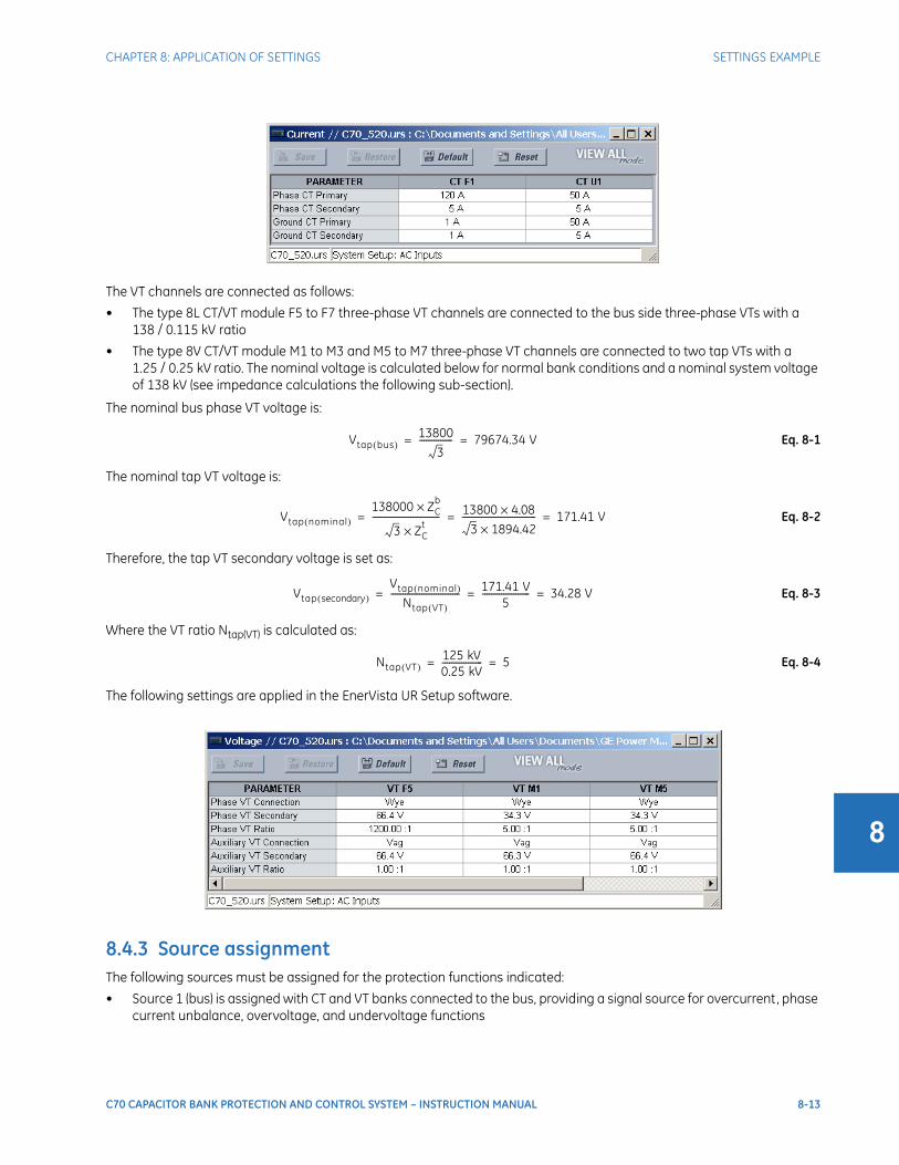
CHAPTER 8: APPLICATION OF SETTINGS SETTINGS EXAMPLE
C70 CAPACITOR BANK PROTECTION AND CONTROL SYSTEM – INSTRUCTION MANUAL 8-13
8
The VT channels are connected as follows:
• The type 8L CT/VT module F5 to F7 three-phase VT channels are connected to the bus side three-phase VTs with a 138 / 0.115 kV ratio
• The type 8V CT/VT module M1 to M3 and M5 to M7 three-phase VT channels are connected to two tap VTs with a 1.25 / 0.25 kV ratio. The nominal voltage is calculated below for normal bank conditions and a nominal system voltage of 138 kV (see impedance calculations the following sub-section).
The nominal bus phase VT voltage is:
Eq. 8-1
The nominal tap VT voltage is:
Eq. 8-2
Therefore, the tap VT secondary voltage is set as:
Eq. 8-3
Where the VT ratio Ntap(VT) is calculated as:
Eq. 8-4
The following settings are applied in the EnerVista UR Setup software.
8.4.3 Source assignmentThe following sources must be assigned for the protection functions indicated:
• Source 1 (bus) is assigned with CT and VT banks connected to the bus, providing a signal source for overcurrent, phase current unbalance, overvoltage, and undervoltage functions
Vtap bus( )13800
3-------------- 79674.34 V= =
Vtap nominal( )138000 ZC
b×
3 ZCt×
---------------------------- 13800 4.08×3 1894.42×
------------------------------- 171.41 V= = =
Vtap secondary( )Vtap nominal( )
Ntap VT( )----------------------------- 171.41 V
5-------------------- 34.28 V= = =
Ntap VT( )125 kV0.25 kV----------------- 5= =
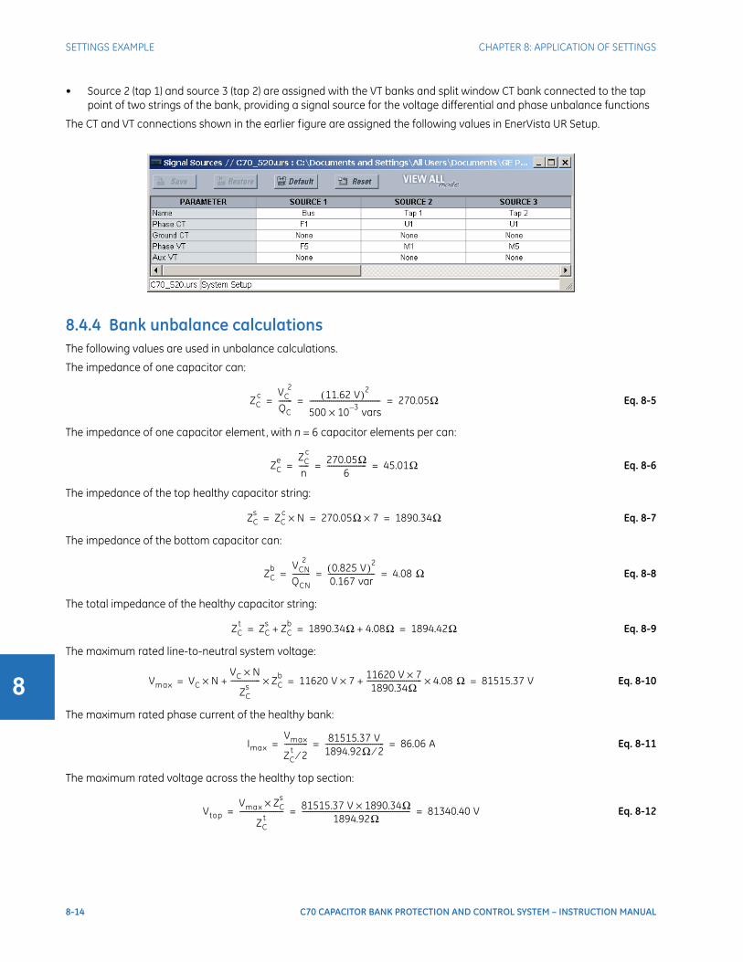
8-14 C70 CAPACITOR BANK PROTECTION AND CONTROL SYSTEM – INSTRUCTION MANUAL
SETTINGS EXAMPLE CHAPTER 8: APPLICATION OF SETTINGS
8
• Source 2 (tap 1) and source 3 (tap 2) are assigned with the VT banks and split window CT bank connected to the tap point of two strings of the bank, providing a signal source for the voltage differential and phase unbalance functions
The CT and VT connections shown in the earlier figure are assigned the following values in EnerVista UR Setup.
8.4.4 Bank unbalance calculationsThe following values are used in unbalance calculations.
The impedance of one capacitor can:
Eq. 8-5
The impedance of one capacitor element, with n = 6 capacitor elements per can:
Eq. 8-6
The impedance of the top healthy capacitor string:
Eq. 8-7
The impedance of the bottom capacitor can:
Eq. 8-8
The total impedance of the healthy capacitor string:
Eq. 8-9
The maximum rated line-to-neutral system voltage:
Eq. 8-10
The maximum rated phase current of the healthy bank:
Eq. 8-11
The maximum rated voltage across the healthy top section:
Eq. 8-12
ZCc VC
2
QC------- 11.62 V( )2
500 10 3–× vars------------------------------------ 270.05Ω= = =
ZCe ZC
c
n----- 270.05Ω
6-------------------- 45.01Ω= = =
ZCs ZC
c N× 270.05Ω 7× 1890.34Ω= = =
ZCb VCN
2
QCN--------- 0.825 V( )2
0.167 var------------------------ 4.08 Ω= = =
ZCt ZC
s ZCb+ 1890.34Ω 4.08Ω+ 1894.42Ω= = =
Vmax VC N×VC N×
ZCs
--------------- ZCb×+ 11620 V 7× 11620 V 7×
1890.34Ω---------------------------- 4.08 Ω×+ 81515.37 V= = =
ImaxVmax
ZCt 2⁄
------------ 81515.37 V1894.92Ω 2⁄------------------------------ 86.06 A= = =
VtopVmax ZC
s×
ZCt
---------------------- 81515.37 V 1890.34Ω×1894.92Ω
------------------------------------------------------- 81340.40 V= = =

CHAPTER 8: APPLICATION OF SETTINGS SETTINGS EXAMPLE
C70 CAPACITOR BANK PROTECTION AND CONTROL SYSTEM – INSTRUCTION MANUAL 8-15
8
The maximum rated voltage across the healthy bottom section:
Eq. 8-13
The voltage distribution factor for the healthy perfectly balanced bank for the 87V-2 and 87V-3 elements:
Eq. 8-14
The impedance of the string for the failed capacitors elements (for one failed element, nf = 1:
Eq. 8-15
The voltage at the tap in the section with one failed capacitor element in the string:
Eq. 8-16
The voltage of the top section with one capacitor element failed:
Eq. 8-17
The overvoltage at the affected capacitors with one capacitor element failed:
Eq. 8-18
The differential voltage between two taps with one failed capacitor element in the upper string, assuming K = 1 for 87V-1, in per-unit values is:
Eq. 8-19
The differential voltage between the bus voltage and the tap with one failed capacitor element in the upper string, assuming K = 1, for 87V-3 in per-unit values is:
Eq. 8-20
The unbalance current in the window type CT between two strings with one failed capacitor element in the upper string:
Eq. 8-21
The following table summarizes the calculated values for the number of failed capacitors used to set the protection elements.
VbottomVmax ZC
b×
ZCt
---------------------- 81515.37 V 4.08 Ω×1894.92Ω
------------------------------------------------ 175.37 V= = =
KtapVtop
Vbottom----------------- 81340.40 V
175.37 V-------------------------- 463.8194= = =
ZCsf ZC
e N n× nf–( ) ZCb+ 45.01Ω 7 6× 1–( ) 4.08 Ω+× 1849.41Ω= = =
Vtap2Vmax ZC
b×
ZCsf
---------------------- 81515.37 V 4.08 Ω×1849.91 Ω
------------------------------------------------ 179.64 V= = =
Vtop Vmax Vtap2–=
OVVf top( ) N n××
Vtop N n× nf–( )×------------------------------------------ 81335.74 V 7× 6×
81340.40 V 7 6× 1–( )×-------------------------------------------------------- 1.024 pu= = =
Vdiff tap( )Vtap1 1 Vtap2×–
VTnom tap( )--------------------------------------- 175.374 V 1 179.64 V×–
171.59 V---------------------------------------------------------- 0.0249 pu= = =
Vdiff string( )Vf top( ) Ktap Vtap2×–
VTnom bus( )------------------------------------------------ 175.374 V 463.8194 179.64 V×–
79674.34 V----------------------------------------------------------------------------- 0.0249 pu= = =
IunbalVmax
ZCsf CTtap×
------------------------Vmax
ZCs CTtap×
-----------------------– 81515.37 V1845.33Ω 50×----------------------------------- 81515.37 V
1890.34Ω 50×-----------------------------------– 0.0209 pu= = =

8-16 C70 CAPACITOR BANK PROTECTION AND CONTROL SYSTEM – INSTRUCTION MANUAL
SETTINGS EXAMPLE CHAPTER 8: APPLICATION OF SETTINGS
8
Table 8-1: Unbalance values for maximum system conditions
To check the limits of protection sensitivity, the same calculations are repeated for the minimum system conditions, which are considered to be 0.85 pu of nominal system voltage.
The minimum line to neutral system voltage is:
Eq. 8-22
The following table summarizes the unbalance values during minimum system conditions.
Table 8-2: Unbalance values for minimum system conditions
The balance values during minimum operating conditions can be used to check sensitivity.
8.4.5 Bank voltage differential settingsThe bank configuration, CT location, and VT locations allow applying three voltage differential elements:
• An 87V-1 differential element measuring the differential voltage between the two bottom taps
• An 87V-2 differential element measuring the differential voltage between the upper capacitor string and bottom capacitor can for string 1
• An 87V-3 differential element measuring the differential voltage between the upper capacitor string and bottom capacitor can for string 2
0 1894.42 Ω 1894.42 Ω 175.37 V 175.37 V 81340.00 V 1.000 pu 0.0000 pu 0.0000 pu 0.0000 pu
1 1894.42 Ω 1849.41 Ω 175.37 V 179.64 V 81335.73 V 1.024 pu 0.0249 pu 0.0249 pu 0.0209 pu
2 1894.42 Ω 1804.40 Ω 175.37 V 184.12 V 81331.25 V 1.050 pu 0.0510 pu 0.0510 pu 0.0429 pu
3 1894.42 Ω 1759.39 Ω 175.37 V 188.83 V 81326.54 V 1.077 pu 0.0785 pu 0.0785 pu 0.0660 pu
4 1894.42 Ω 1714.38 Ω 175.37 V 193.79 V 81321.58 V 1.105 pu 0.1074 pu 0.1074 pu 0.0904 pu
5 1894.42 Ω 1669.38 Ω 175.37 V 199.01 V 81316.36 V 1.135 pu 0.1379 pu 0.1379 pu 0.1160 pu
6 1894.42 Ω 1624.37 Ω 175.37 V 204.52 V 81310.85 V 1.167 pu 0.1701 pu 0.1701 pu 0.1431 pu
7 1894.42 Ω 1579.36 Ω 175.37 V 210.35 V 81305.02 V 1.200 pu 0.2041 pu 0.2041 pu 0.1717 pu
8 1894.42 Ω 1534.35 Ω 175.37 V 216.52 V 81298.85 V 1.235 pu 0.2401 pu 0.2401 pu 0.2020 pu
9 1894.42 Ω 1489.34 Ω 175.37 V 223.07 V 81292.30 V 1.273 pu 0.2783 pu 0.2783 pu 0.2341 pu
10 1894.42 Ω 1444.34 Ω 175.37 V 230.02 V 81285.35 V 1.313 pu 0.3188 pu 0.3188 pu 0.2682 pu
0 1894.42 Ω 1894.42 Ω 145.70 V 145.70 V 67577.30 V 1.000 pu 0.0000 pu 0.0000 pu 0.0000 pu
1 1894.42 Ω 1849.41 Ω 145.70 V 149.24 V 67573.76 V 1.024 pu 0.0207 pu 0.0207 pu 0.0174 pu
2 1894.42 Ω 1804.40 Ω 145.70 V 152.97 V 67570.03 V 1.050 pu 0.0424 pu 0.0424 pu 0.0357 pu
3 1894.42 Ω 1759.39 Ω 145.70 V 156.88 V 67566.12 V 1.077 pu 0.0652 pu 0.0652 pu 0.0549 pu
4 1894.42 Ω 1714.38 Ω 145.70 V 161.00 V 67562.00 V 1.105 pu 0.0893 pu 0.0893 pu 0.0751 pu
5 1894.42 Ω 1669.38 Ω 145.70 V 165.34 V 67557.66 V 1.135 pu 0.1146 pu 0.1146 pu 0.0964 pu
6 1894.42 Ω 1624.37 Ω 145.70 V 169.92 V 67553.08 V 1.167 pu 0.1413 pu 0.1413 pu 0.1189 pu
7 1894.42 Ω 1579.36 Ω 145.70 V 174.76 V 67548.24 V 1.200 pu 0.1696 pu 0.1696 pu 0.1426 pu
8 1894.42 Ω 1534.35 Ω 145.70 V 179.89 V 67543.11 V 1.235 pu 0.1995 pu 0.1995 pu 0.1678 pu
9 1894.42 Ω 1489.34 Ω 145.70 V 185.32 V 67537.68 V 1.273 pu 0.2312 pu 0.2312 pu 0.1945 pu
10 1894.42 Ω 1444.34 Ω 145.70 V 191.10 V 67531.90 V 1.313 pu 0.2649 pu 0.2649 pu 0.2228 pu
nf ZCs ZC
sf Vtap1 Vtap2 Vtop OV Vdiff tap( ) Vdiff string( ) Iunbal
Vmin0.85 Vnom×
3--------------------------- 0.85 138000 V×
3-------------------------------------- 67723 V= = =
nf ZCs ZC
sf Vtap1 Vtap2 Vtop OV Vdiff tap( ) Vdiff string( ) Iunbal

CHAPTER 8: APPLICATION OF SETTINGS SETTINGS EXAMPLE
C70 CAPACITOR BANK PROTECTION AND CONTROL SYSTEM – INSTRUCTION MANUAL 8-17
8
Two voltage differential (87V) stages provide trip and alarm levels during capacitor unit failures in each differential element. The capacitor units are subject to overvoltage if one or more capacitors units are shorted out. The voltage differential trip pickup setting is programmed for value of 110% of capacitor rated voltage. As seen from the previous Unbalance Values for Maximum System Conditions table, a failure of four capacitor elements causes a 10.5% overvoltage.
The pickup setting for the stage 1 differential alarm element is chosen for one element failure.
Eq. 8-23
The alarm delay is set to 10 seconds to avoid alarming during transient conditions.
The pickup setting for the stage 2 differential trip element is programmed as the differential voltage during maximum system conditions midway between the third and fourth capacitor element failure differential voltages.
Eq. 8-24
Therefore, the trip delay is set to 50 ms.
The following setting values for the voltage differential 1 element between two tap voltages are programmed in the EnerVista UR Setup software.
Note that match factor shown above assumes perfect bank balance. This must be adjusted when the bank is energized during the differential function auto-setting procedure tune up.
The voltage differential element must be blocked during a VT fuse failure at any tap. The voltage differential element is dependent on both source VTs. These VTs must be blocked if one or both of them has a VT fuse failure condition. Therefore, as shown in the following figure, a blocking input for each element is created with FlexLogic.
87V alarm 0.9Vdiff f1_max( ) 0.9 0.0249 pu× 0.0224 pu= = =
87V tripVdiff f4_max( ) Vdiff f3_max( )+
2----------------------------------------------------------- 0.1074 pu 0.0785 pu+
2---------------------------------------------------- 0.093 pu= = =
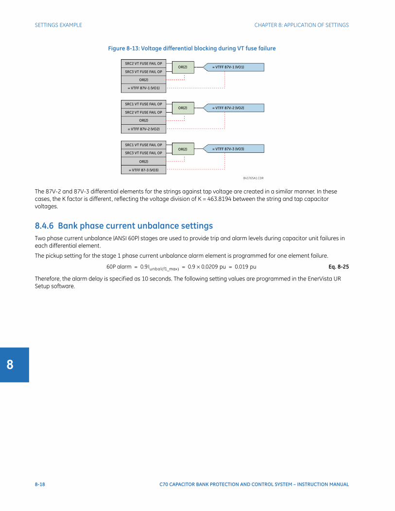
8-18 C70 CAPACITOR BANK PROTECTION AND CONTROL SYSTEM – INSTRUCTION MANUAL
SETTINGS EXAMPLE CHAPTER 8: APPLICATION OF SETTINGS
8
Figure 8-13: Voltage differential blocking during VT fuse failure
The 87V-2 and 87V-3 differential elements for the strings against tap voltage are created in a similar manner. In these cases, the K factor is different, reflecting the voltage division of K = 463.8194 between the string and tap capacitor voltages.
8.4.6 Bank phase current unbalance settingsTwo phase current unbalance (ANSI 60P) stages are used to provide trip and alarm levels during capacitor unit failures in each differential element.
The pickup setting for the stage 1 phase current unbalance alarm element is programmed for one element failure.
Eq. 8-25
Therefore, the alarm delay is specified as 10 seconds. The following setting values are programmed in the EnerVista UR Setup software.
SRC2 VT FUSE FAIL OP
SRC3 VT FUSE FAIL OP
OR(2)
= VTFF 87V-1 (VO1)
SRC1 VT FUSE FAIL OP
SRC2 VT FUSE FAIL OP
OR(2)
= VTFF 87V-2 (VO2)
SRC1 VT FUSE FAIL OP
SRC3 VT FUSE FAIL OP
OR(2)
= VTFF 87-3 (VO3)
OR(2)
OR(2)
OR(2)
= VTFF 87V-1 (VO1)
= VTFF 87V-2 (VO2)
= VTFF 87V-3 (VO3)
843765A1.CDR
60P alarm 0.9Iunbal f1_max( ) 0.9 0.0209 pu× 0.019 pu= = =

CHAPTER 8: APPLICATION OF SETTINGS SETTINGS EXAMPLE
C70 CAPACITOR BANK PROTECTION AND CONTROL SYSTEM – INSTRUCTION MANUAL 8-19
8
The pickup setting for the stage 2 current unbalance trip element is specified as the unbalance current during maximum system conditions midway between the third and fourth capacitor element failure unbalance currents.
Eq. 8-26
Therefore, the trip delay is chosen 50 ms.
8.4.7 Bank phase overvoltage settingsTo protect the capacitor bank from overvoltage resulting from abnormal system conditions, the capability of the bank to withstand transient overvoltages must be evaluated according to the IEEE 1036-1992 standard or to manufacturer specifications. For example, consider the following manufacturer overvoltage data:
• 2 pu overvoltage toleration for 0.25 second
• 1.5 pu overvoltage toleration for 15 seconds
• 1.25 pu overvoltage toleration for 5 minutes
When the relay settings are calculated, the number of prospective overvoltage transients stressing the capacitor insulation during the bank lifetime must be taken into account. As such, it is preferable to set the relay conservatively.
60P tripIunbal f4_max( ) Iunbal f3_max( )+
2----------------------------------------------------------------- 0.0904 pu 0.0660 pu+
2---------------------------------------------------- 0.078 pu= = =

8-20 C70 CAPACITOR BANK PROTECTION AND CONTROL SYSTEM – INSTRUCTION MANUAL
SETTINGS EXAMPLE CHAPTER 8: APPLICATION OF SETTINGS
8
Based on the manufacturer overvoltage data outlined, three overvoltage trip stages are applied using a factor of 0.9 for the stage pickup overvoltage levels and half of the allowable time outlined.
Eq. 8-27
Eq. 8-28
The following setting values are programmed in the EnerVista UR Setup software.
8.4.8 Bank phase undervoltage settingsBank undervoltage protection is required to take bank out-of-service when the supply bus voltage is lost. The pickup setting is specified as 0.7 pu with a time delay of 1 second, based on maximum fault clearing time. The bank undervoltage element is blocked during VT fuse fail conditions.
The following setting values are programmed in the EnerVista UR Setup software.
59B pickup (stage 1) 0.9 1.25× 1.125 pu= =
59B pickup (stage 2) 0.9 1.5× 1.35 pu= =
59B pickup (stage 3) 0.9 2× 1.80 pu= =
59B delay (stage 1) 0.5 5 60×× 150 seconds= =
59B delay (stage 2) 0.5 15× 7.5 seconds= =
59B delay (stage 3) 0.5 0.25× 0.125 seconds= =
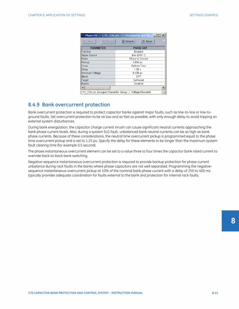
CHAPTER 8: APPLICATION OF SETTINGS SETTINGS EXAMPLE
C70 CAPACITOR BANK PROTECTION AND CONTROL SYSTEM – INSTRUCTION MANUAL 8-21
8
8.4.9 Bank overcurrent protectionBank overcurrent protection is required to protect capacitor banks against major faults, such as line-to-line or line-to-ground faults. Set overcurrent protection to be as low and as fast as possible, with only enough delay to avoid tripping on external system disturbances.
During bank energization, the capacitor charge current inrush can cause significant neutral currents approaching the bank phase current levels. Also, during a system SLG fault, unbalanced bank neutral currents can be as high as bank phase currents. Because of these considerations, the neutral time overcurrent pickup is programmed equal to the phase time overcurrent pickup and is set to 1.25 pu. Specify the delay for these elements to be longer than the maximum system fault clearing time (for example 0.5 second).
The phase instantaneous overcurrent element can be set to a value three to four times the capacitor bank rated current to override back-to-back bank switching.
Negative-sequence instantaneous overcurrent protection is required to provide backup protection for phase current unbalance during rack faults in the banks where phase capacitors are not well separated. Programming the negative-sequence instantaneous overcurrent pickup at 10% of the nominal bank phase current with a delay of 250 to 400 ms typically provides adequate coordination for faults external to the bank and protection for internal rack faults.

8-22 C70 CAPACITOR BANK PROTECTION AND CONTROL SYSTEM – INSTRUCTION MANUAL
SETTINGS EXAMPLE CHAPTER 8: APPLICATION OF SETTINGS
8
C70 CAPACITOR BANK PROTECTION AND CONTROL SYSTEM – INSTRUCTION MANUAL 9-1
C70 Capacitor Bank Protection and Control System
Chapter 9: Theory of operation
Theory of operation
This chapter outlines advanced information on operation.
9.1 Overview
9.1.1 General operationStatic capacitor banks are constructed with a large number of individual capacitor elements connected in a series/parallel arrangement designed to distribute the system voltage equally among the elements. Equal distribution of voltage is important as the rate of internal insulation degradation is a highly non-linear function of element voltage, with degradation accelerating very rapidly with overvoltage greater than 10%. To obtain balanced voltages in spite of manufacturing tolerances in the capacitance of the elements, the elements are positioned in the bank according to their actual capacitance such that parallel groups have a uniform total capacitance, and a good voltage balance is obtained. However, once in service, individual elements can fail randomly upsetting the balance, increasing the stress on other elements, and causing their early failure. Early failure of an element due to unbalanced voltage predictably further unbalances the bank, leading to cascading failure.
The purpose of capacitor unbalance protection is to detect unbalance caused by element failures as soon as practical, and to either alarm the condition so that repair can be scheduled for a convenient time, or to automatically remove the bank from service to prevent deterioration in the healthy elements pending repair. A brut force method is to directly measure the voltage across each element, operating on detecting an abnormally high voltage on any element. However, this approach is seldom economic due to the large number of voltage transducers required. Thus, the C70 supports various other methods, the suitability of each dependant on the capacitor bank configuration, and on the VTs and CTs available.
The challenge faced by all capacitor unbalance protections not using the brut force method is the increased sensitivity required due to the less than ideal number of monitoring points, and compensation for the increased effects of inherent unbalance due to manufacturing tolerance and due to system voltage unbalance.
9.1.2 Bank phase overvoltage (ANSI 59B)The capacitor unbalance protection functions discussed in the following sections are intended to detect failures in the capacitor bank itself that can result in a few capacitor elements being overstressed. However, these unbalance protection functions do not detect overstressed elements in a healthy bank that can result from external problems. Protection against overstressing elements from system overvoltages is instead provided by the bank phase overvoltage protection.

9-2 C70 CAPACITOR BANK PROTECTION AND CONTROL SYSTEM – INSTRUCTION MANUAL
OVERVIEW CHAPTER 9: THEORY OF OPERATION
9
Ideally, a bank overvoltage protection measures the voltage across each capacitor string, allowing an accurate inference of the voltage across each element in the string, assuming that the string voltage is equally divided across the elements. This is readily done in grounded wye capacitor banks by simply measuring the three system phase-to-ground voltages. For instance, assuming that the bank is healthy, the elements shown in the grounded banks of the following figure are each stressed at one-ninth of system phase-to-ground voltage, allowing the inference that the elements are overstressed when the system phase-to-ground voltage exceeds nine times the element safe operating voltage limit. The true RMS value of these phase-to-ground quantities are what the bank phase overvoltage protection measures when the bus source is set for wye VTs and the bank overvoltage protection ground setpoint is set to grounded.
Figure 9-1: Bank overvoltage protection for grounded and ungrounded banks
For a capacitor bank that is ungrounded, the voltage across the string is equal to the difference between the system phase-to-ground voltage and the bank neutral voltage. Elements shown in the ungrounded banks in the preceding figure are overstressed when the following quantities exceed nine times the element safe operating voltage limit.
Eq. 9-1
These quantities are what the bank phase overvoltage protection measures when the bus source is set for wye VTs, the auxiliary channel of the neutral source is set for a neutral voltage, and the bank overvoltage protection ground setpoint is set to ungrounded.
When the neutral voltage of an ungrounded wye capacitor bank is not measured or you do not want to use the neutral voltage measurement, the string voltage can still be determined using the assumption that the bank is balanced. For an balanced ungrounded bank the neutral voltage VX is:
Eq. 9-2
As such, the A-string voltage is:
Eq. 9-3
834744A1.CDR
Grounded bank
VA
A
B
C
VB
VC
VX
VA
A
B
C
VB
VC
Ungrounded bank
VA VX– RMS, VB VX– RMS, or VC VX– RMS
VX13-- VA VB VC+ +( )=
VA VX– RMS VA13-- VA VB VC+ +( )–
RMS=
13-- 2VA VB VC–– RMS=
13-- VAB VCA– RMS=

CHAPTER 9: THEORY OF OPERATION OVERVIEW
C70 CAPACITOR BANK PROTECTION AND CONTROL SYSTEM – INSTRUCTION MANUAL 9-3
9
Similarly, the B-string and C-string voltages are:
Eq. 9-4
These quantities are what the bank phase overvoltage protection measures when the bus source is set for wye VTs, and the bank overvoltage protection ground setpoint is set to “Ungrd w/o Vn.”
In applications where the bus VTs are delta-connected, the bus phase-to-ground voltages and therefore the bus zero sequence voltage are unknown. However, as shown in the preceding equations, string voltages can be determined for an ungrounded balanced bank using only phase-to-phase bus voltages. In the case of a grounded bank, we can calculate that the A-string voltage is:
Eq. 9-5
If we make the assumption that the zero-sequence voltage is negligible, which is reasonable when the system is normal (non-faulted), then the string voltages for grounded banks are the same as for the ungrounded balanced banks:
Eq. 9-6
These quantities are what the bank phase overvoltage protection measures whenever the bus source is set for delta VTs.
9.1.3 Voltage differential (ANSI 87V)
9.1.3.1 Operating principleThe voltage differential function is based on a voltage divider principle. A healthy capacitor string has a constant and known match factor between its full tap (typically the bus voltage) and an auxiliary tap used by the protection. Any single element failure results in a difference between the measured factor and its value when the bank is healthy. The protection can be used on both grounded and ungrounded banks. For ungrounded banks, the neutral point voltage (VX) must be measured by the relay and used to derive the voltage across the string.
13-- VBC VAB– RMS and 1
3-- VCA VBC– RMS
VA RMS13-- 3VA VB VB–( ) VC VC–( )+ + RMS=
13-- VA VB– VC– VA VA VB VC+ +( )+ + RMS=
13-- VAB VCA– 3V0+ RMS=
13-- VAB VCA– RMS, 1
3-- VBC VAB– RMS, or 1
3-- VCA VBC– RMS

9-4 C70 CAPACITOR BANK PROTECTION AND CONTROL SYSTEM – INSTRUCTION MANUAL
OVERVIEW CHAPTER 9: THEORY OF OPERATION
9
Figure 9-2: Voltage differential application to grounded and ungrounded banks
The voltage differential protection uses the following operating signal for grounded banks:
Eq. 9-7
The voltage differential protection uses the following operating signal for ungrounded banks:
Eq. 9-8
In these equations, kA is a match factor setting for the A-leg of the bank. The voltages are as defined in the preceding figure and are in per-unit values on the nominal bus phase-to-ground voltage base. The first equation is implemented using primary voltage magnitudes, while the second equation is implemented using primary voltage phasors. The protection operates when the operate signal is greater than the set pickup level for the set pickup delay.
Identical relations apply to phases B and C.
Sensitivity is the key performance parameter. The applied comparator uses a simple integration method in addition to the standard hysteresis approach, to deal with chattering of the operating signal at the boundary of operation.
9.1.3.2 Balanced caseTo understand how the voltage differential protection works, consider for simplicity the following grounded bank operating equation:
Eq. 9-9
The ungrounded case is similar except that all voltages have VX subtracted. If the initial factory balanced A-leg string has an initial capacitance of CA, divided into sub-strings with initial capacitances of C1A and C2A, and the bank is energized with system phase-to-ground voltage VSpg, then the string forms a voltage divider and the initial measured voltages are:
Eq. 9-10
Eq. 9-11
834750A1.CDR
Grounded bank Ungrounded bank
V2A
V1A
A
B
C
C1A
C2A
CA
VX
V2A
V1A
A
B
C
C1A
C2A
CA
VOP A( ) V1A kAV2A–=
VOP A( ) V1A VX–( ) kA V2A VX–( )–=
VOP A( ) V1A kAV2A–=
V1A VSpg=
V2A VSpg
CA
C2A--------×=

CHAPTER 9: THEORY OF OPERATION OVERVIEW
C70 CAPACITOR BANK PROTECTION AND CONTROL SYSTEM – INSTRUCTION MANUAL 9-5
9
Substituting these results into the first equation, the initial operating signal is:
Eq. 9-12
The match factor setting kA is chosen as:
Eq. 9-13
Therefore, as can be seen from the previous two equations, the initial operating signal is zero.
9.1.3.3 SensitivityNow consider the consequences of an element failure in the upper sub-string of leg A, making a small capacitance change in C1A. The effect on the operating signal can be calculated by taking the derivative of equation 9-12 with respect to CA, holding C2A constant. In the general case, the derivative of the absolute value function is messy, but in our case where the initial value is zero, the derivative of the absolute function is simply the absolute value of the derivative of its argument. The derivative is thus:
Eq. 9-14
Substituting equation 9-13, we have:
Eq. 9-15
This can be written as:
Eq. 9-16
In this equation, ΔCA(pu) is the capacitance change as a per-unit of the leg capacitance, VSpg is the system phase-to-ground voltage, and VOP(1A)(pu) is the operating signal resulting from the failure in the upper sub-string. Both voltages are in per-unit of nominal bus phase-to-ground voltage, so VSpg can be taken as 1 when the system is normal (not faulted). Note however that under external fault conditions, sensitivity can be much different from the non-fault sensitivity.
Instead of a failure in the upper sub-string, now suppose a failure in the lower sub-string. The same approach is used, except to make the algebra easier, the initial operating signal is converted to be in terms of C1A using:
Eq. 9-17
In this case, we have:
Eq. 9-18
VOP A( ) V1A kAV2A–=
VSpg kAVSpg
CA
C2A--------×–=
VSpg 1 kA
CA
C2A--------×–×=
kAC2A
CA--------=
ddCA---------VOP 1A( ) VSpg
ddCA--------- 1 kA
CA
C2A--------–
×=
VSpg
kA
C2A--------–×=
VSpg
kA
C2A--------×=
ddCA---------VOP 1A( ) VSpg
1CA-----×= or dVOP 1A( ) VSpg
dCA
CA---------×=
VOP 1A( ) pu( ) VSpg pu( ) CAΔ× pu( )=
CAC1AC2A
C1A C2A+----------------------= or C2A
CAC1A
C1A CA–-------------------=
VOP A( ) VSpg 1 kA
CA
C2A--------×–×=
VSpg 1 kA
C1A CA–
C1A-------------------×–×=
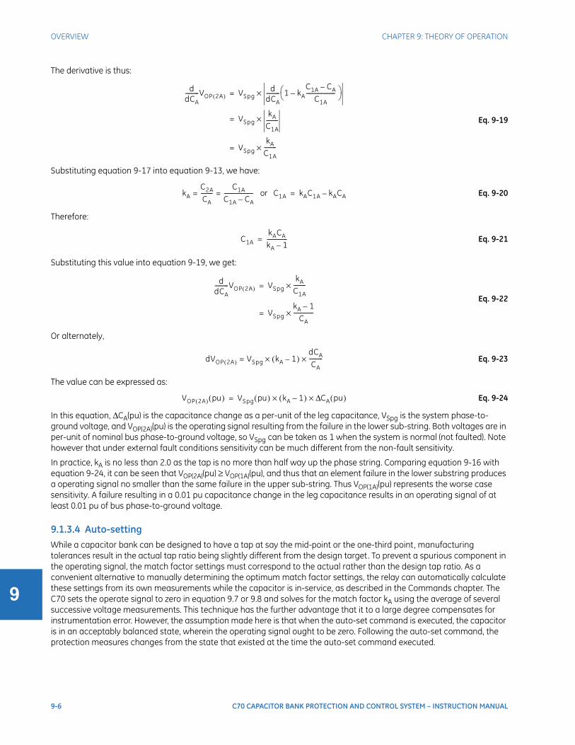
9-6 C70 CAPACITOR BANK PROTECTION AND CONTROL SYSTEM – INSTRUCTION MANUAL
OVERVIEW CHAPTER 9: THEORY OF OPERATION
9
The derivative is thus:
Eq. 9-19
Substituting equation 9-17 into equation 9-13, we have:
Eq. 9-20
Therefore:
Eq. 9-21
Substituting this value into equation 9-19, we get:
Eq. 9-22
Or alternately,
Eq. 9-23
The value can be expressed as:
Eq. 9-24
In this equation, ΔCA(pu) is the capacitance change as a per-unit of the leg capacitance, VSpg is the system phase-to-ground voltage, and VOP(2A)(pu) is the operating signal resulting from the failure in the lower sub-string. Both voltages are in per-unit of nominal bus phase-to-ground voltage, so VSpg can be taken as 1 when the system is normal (not faulted). Note however that under external fault conditions sensitivity can be much different from the non-fault sensitivity.
In practice, kA is no less than 2.0 as the tap is no more than half way up the phase string. Comparing equation 9-16 with equation 9-24, it can be seen that VOP(2A)(pu) ≥ VOP(1A)(pu), and thus that an element failure in the lower substring produces a operating signal no smaller than the same failure in the upper sub-string. Thus VOP(1A)(pu) represents the worse case sensitivity. A failure resulting in a 0.01 pu capacitance change in the leg capacitance results in an operating signal of at least 0.01 pu of bus phase-to-ground voltage.
9.1.3.4 Auto-settingWhile a capacitor bank can be designed to have a tap at say the mid-point or the one-third point, manufacturing tolerances result in the actual tap ratio being slightly different from the design target. To prevent a spurious component in the operating signal, the match factor settings must correspond to the actual rather than the design tap ratio. As a convenient alternative to manually determining the optimum match factor settings, the relay can automatically calculate these settings from its own measurements while the capacitor is in-service, as described in the Commands chapter. The C70 sets the operate signal to zero in equation 9.7 or 9.8 and solves for the match factor kA using the average of several successive voltage measurements. This technique has the further advantage that it to a large degree compensates for instrumentation error. However, the assumption made here is that when the auto-set command is executed, the capacitor is in an acceptably balanced state, wherein the operating signal ought to be zero. Following the auto-set command, the protection measures changes from the state that existed at the time the auto-set command executed.
ddCA---------VOP 2A( ) VSpg
ddCA--------- 1 kA
C1A CA–
C1A-------------------–
×=
VSpgkA
C1A--------×=
VSpg
kA
C1A--------×=
kAC2A
CA--------
C1A
C1A CA–-------------------= = or C1A kAC1A kACA–=
C1AkACA
kA 1–-------------=
ddCA---------VOP 2A( ) VSpg
kA
C1A--------×=
VSpg
kA 1–
CA-------------×=
dVOP 2A( ) VSpg= kA 1–( )dCA
CA---------××
VOP 2A( ) pu( ) VSpg pu( ) kA 1–( )× CAΔ× pu( )=

CHAPTER 9: THEORY OF OPERATION OVERVIEW
C70 CAPACITOR BANK PROTECTION AND CONTROL SYSTEM – INSTRUCTION MANUAL 9-7
9
9.1.4 Compensated bank neutral voltage unbalance (ANSI 59NU)
9.1.4.1 Operating principleThe neutral voltage unbalance function is applicable to ungrounded banks. Fundamentally, this function responds to an overvoltage condition of the neutral-point voltage. If the capacitor bank and the power system voltages are balanced, the neutral-point voltage is zero. If a capacitor element in the bank fails, then the bank becomes unbalanced and the neutral voltage increases.
The operate signal for the neutral voltage unbalance protection is:
Eq. 9-25
The restraint signal for the neutral voltage unbalance protection is:
Eq. 9-26
In these equations, kAB and kAC represent capacitor bank unbalance ratio settings. The voltages are as defined in the following figure and are expressed in per-units of the nominal value of the neutral-point VT.
These equations involve phasors, not magnitudes. That is, the vector sum of the voltages is created by the protection function implementing the method.
The neutral voltage unbalance protection operates when the operate signal is greater than the set pickup level and the operate signal is greater than the set percentage of the restraint signal, all for the set pickup delay.
Sensitivity is the key performance parameter. The applied comparator uses a simple integration method in addition to the standard hysteresis approach to deal with chattering of the operating signal at the boundary of operation. In addition, a slope characteristic is used to deal with measurement errors for the involved voltages under large system unbalances, such as during a close-in external fault.
Figure 9-3: Compensated bank neutral overvoltage application
VOP13-- VX 1 kAB kAC+ +( ) 3V0– VB 1 kAB–( ) VC 1 kAC–( )+ +=
VREST VX V0+=
834745A1.CDR
VA
-V
X
VA
A
B
C
VX
IC
IB IA
IA
+ IB
+ IC
= 0
CC
CB
CA

9-8 C70 CAPACITOR BANK PROTECTION AND CONTROL SYSTEM – INSTRUCTION MANUAL
OVERVIEW CHAPTER 9: THEORY OF OPERATION
9
9.1.4.2 Balanced caseTo understand neutral voltage unbalance protection, we can start with Kirchhoff's current law for the neutral node of the bank:
Eq. 9-27
This expression can be rearranged as follows.
Eq. 9-28
Multiplying both sides by –1 / CA and substituting the sum of the phase voltages with 3V0 yields:
Eq. 9-29
As the left hand side of this equation is equal to zero, we can subtract it from the expression inside the absolute value brackets in equation 9.25 to get:
Eq. 9-30
The unbalance ratio k-values that reflect the initial or inherent bank unbalance are chosen as:
Eq. 9-31
Therefore, as seen from the previous two equations, the initial operating signal is zero.
Note that the ratios of the capacitances between phase A and the two other phases are close to unity, and therefore the correcting factors in equation 9.25 for the B and C-phase voltages are small numbers, while the factor for the VX voltage is close to 3. If so, equation 9.25 takes a familiar simplified form:
Eq. 9-32
The V0 term in the operate equation can be either the neutral component in the bus voltages (one-third of the vectorial sum of the phase voltages calculated by the relay), or directly measured neutral voltage component (open-corner-delta VT voltage).
9.1.4.3 SensitivityNow consider the consequences of a capacitor element failure in one leg, most conveniently leg C, making a small capacitance change in leg-C capacitance. The effect on the operating signal can be calculated by taking the derivative of equation 9.25 with respect to CC. In the general case, the derivative of the absolute value function is messy, but in our case where the initial value is zero, the derivative of the absolute function is simply the absolute value of the derivative of its argument. As such, the derivative is:
Eq. 9-33
Recall equation 9.29:
Eq. 9-34
IA IB IC+ + jωCA VA VX–( ) jωCB VB VX–( ) jωCC VC VX–( )+ + 0= =
VX CA CB CC+ +( )– VACA VBCB VCCC+ + + 0=
VX CA CB CC+ +( )– VACA VBCA VCCA VBCB VBCA– VCCC VCCA–+ + + + + 0=
VX CA CB CC+ +( )– CA VA VB VC+ +( ) VB CB CA–( ) VC CC CA–( )+ + + 0=
VX 1CB CC+
CA-----------------+
3V0– VB 1CB
CA-----–
VC 1CC
CA-----–
+ + 0=
VOP13-- VX 1 kAB kAC+ +( ) 3V0– VB 1 kAB–( ) VC 1 kAC–( ) V– X 1
CB CC+
CA-----------------+
3V0 VB– 1CB
CA-----–
VC– 1CC
CA-----–
++ +=
13-- VX kAB
CB
CA-----– kAC
CC
CA-----–+
VBCB
CA----- kAB– VC
CC
CA----- kAC– + +=
kABCB
CA-----, kAC
CC
CA-----= =
VOP VX V0–=
ddCC---------VOP
13-- d
dCC--------- VX 1 kAB kAC+ +( ) 3V0– VB 1 kAB–( ) VC 1 kAC–( )+ +( )=
13-- 1 kAB kAC+ +( )
dVX
dCC---------=
VX 1CB CC+
CA-----------------+
3V0– VB 1CB
CA-----–
VC 1CC
CA-----–
+ + 0=

CHAPTER 9: THEORY OF OPERATION OVERVIEW
C70 CAPACITOR BANK PROTECTION AND CONTROL SYSTEM – INSTRUCTION MANUAL 9-9
9
Differentiating this gives:
Eq. 9-35
Substituting for VX from equation 9.34 gives:
Eq. 9-36
This can be substituted into equation 9.33 to obtain:
Eq. 9-37
For our purposes, , so and . This results in:
Eq. 9-38
Under normal system conditions (non-fault), VC >> V0, and VC is the system phase-to-ground voltage. The system voltage VSpg, which by convention is on the bus voltage base, converted to the base of nominal value of the neutral-point VT used in these equations, is:
Eq. 9-39
This gives:
Eq. 9-40
This can be written as:
Eq. 9-41
In these equations, ΔC(pu) is the capacitance change as a per-unit of the leg capacitance, and VOP(pu) is the operating signal resulting from the failure in per-unit of the nominal value of the neutral-point VT. VSpg is the system phase-to-ground voltage in per-unit of the nominal system phase-to-ground voltage, so can be taken as 1 when the system is normal (not faulted). Note however that under external fault conditions sensitivity can be much different from the non-fault sensitivity. nbus_phs and nntrl_aux are the VT ratios of the phase VT bank of the bus source and of the auxiliary VT channel of the neutral source, respectively.
Note that under external fault conditions sensitivity can be much different form the non-fault sensitivity. To prevent mis-operation, use a restraint and/or coordinating time delay.
dVX
dCC--------- 1
CB CC+
CA-----------------+
VX1
CA----- VC–
1CA----- + 0=
ddCC---------VX
VX VC–
CA 1CB CC+
CA-----------------+
-------------------------------------–=
ddCC---------VX
VX VC–
CA 1 kAB kAC+ +( )----------------------------------------–=
ddCC---------VX
3V0 VB 1 kAB–( )– VC 2 kAB+( )–
CA 1 kAB kAC+ +( )2-------------------------------------------------------------------------=
ddCC---------VOP
13-- 1 kAB kAC+ +( )
dVX
dCC---------=
13--
3V0 VB 1 kAB–( )– VC 2 kAB+( )–
CA 1 kAB kAC+ +( )-------------------------------------------------------------------------=
CA CB CC≅ ≅ kAB 1≅ kAC 1≅
ddCC---------VOP
13--
VC V0–
CC----------------≅
13-- 1
CC----- VC V0–××=
nbus_phs
nntrl_aux------------------ VSpg×
ddCC---------VOP
13-- 1
CC-----
nbus_phs
nntrl_aux------------------ VSpg×××≅
dVOP13--
nbus_phs
nntrl_aux------------------ VSpg××
dCC
CC---------×≅
VOP pu( ) 13--
nbus_phs
nntrl_aux------------------ VSpg×× C pu( )Δ×≅
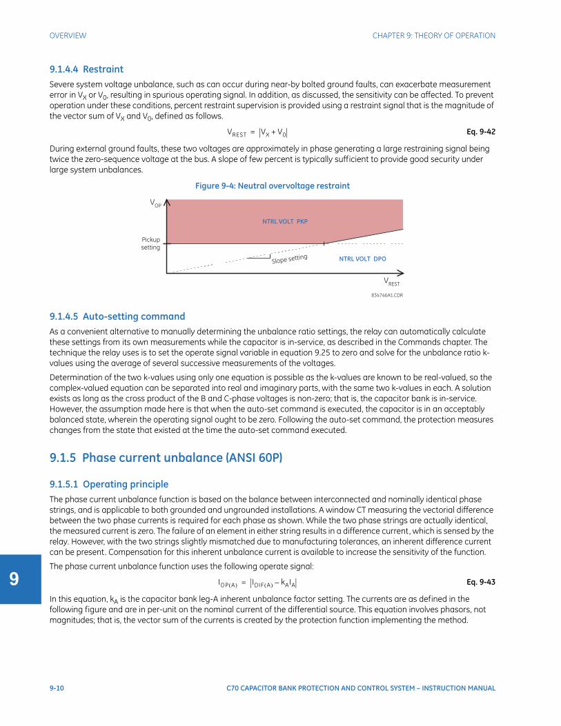
9-10 C70 CAPACITOR BANK PROTECTION AND CONTROL SYSTEM – INSTRUCTION MANUAL
OVERVIEW CHAPTER 9: THEORY OF OPERATION
9
9.1.4.4 RestraintSevere system voltage unbalance, such as can occur during near-by bolted ground faults, can exacerbate measurement error in VX or V0, resulting in spurious operating signal. In addition, as discussed, the sensitivity can be affected. To prevent operation under these conditions, percent restraint supervision is provided using a restraint signal that is the magnitude of the vector sum of VX and V0, defined as follows.
Eq. 9-42
During external ground faults, these two voltages are approximately in phase generating a large restraining signal being twice the zero-sequence voltage at the bus. A slope of few percent is typically sufficient to provide good security under large system unbalances.
Figure 9-4: Neutral overvoltage restraint
9.1.4.5 Auto-setting commandAs a convenient alternative to manually determining the unbalance ratio settings, the relay can automatically calculate these settings from its own measurements while the capacitor is in-service, as described in the Commands chapter. The technique the relay uses is to set the operate signal variable in equation 9.25 to zero and solve for the unbalance ratio k-values using the average of several successive measurements of the voltages.
Determination of the two k-values using only one equation is possible as the k-values are known to be real-valued, so the complex-valued equation can be separated into real and imaginary parts, with the same two k-values in each. A solution exists as long as the cross product of the B and C-phase voltages is non-zero; that is, the capacitor bank is in-service. However, the assumption made here is that when the auto-set command is executed, the capacitor is in an acceptably balanced state, wherein the operating signal ought to be zero. Following the auto-set command, the protection measures changes from the state that existed at the time the auto-set command executed.
9.1.5 Phase current unbalance (ANSI 60P)
9.1.5.1 Operating principleThe phase current unbalance function is based on the balance between interconnected and nominally identical phase strings, and is applicable to both grounded and ungrounded installations. A window CT measuring the vectorial difference between the two phase currents is required for each phase as shown. While the two phase strings are actually identical, the measured current is zero. The failure of an element in either string results in a difference current, which is sensed by the relay. However, with the two strings slightly mismatched due to manufacturing tolerances, an inherent difference current can be present. Compensation for this inherent unbalance current is available to increase the sensitivity of the function.
The phase current unbalance function uses the following operate signal:
Eq. 9-43
In this equation, kA is the capacitor bank leg-A inherent unbalance factor setting. The currents are as defined in the following figure and are in per-unit on the nominal current of the differential source. This equation involves phasors, not magnitudes; that is, the vector sum of the currents is created by the protection function implementing the method.
VREST VX V0+=
834746A1.CDR
VREST
VOP
NTRL VOLT PKP
Slope setting
Pickup
setting
NTRL VOLT DPO
IOP A( ) IDIF A( ) kAIA–=

CHAPTER 9: THEORY OF OPERATION OVERVIEW
C70 CAPACITOR BANK PROTECTION AND CONTROL SYSTEM – INSTRUCTION MANUAL 9-11
9
Figure 9-5: Phase current unbalance application
The protection operates when the operate signal is greater than the set pickup level for the set pickup delay. Identical relations apply to phases B and C.
Sensitivity is the key performance parameter. The applied comparator uses a simple integration method in addition to the standard hysteresis approach, to deal with chattering of the operating signal at the boundary of operation.
9.1.5.2 Balanced caseTo understand phase current unbalance protection, first note that the currents are driven by the individual admittances in each string:
Eq. 9-44
In these equations, Ibase represents the differential CT primary current rating. This places the string currents on the same per-unit base used by the C70. Voltages are expressed in primary volts, capacitances in Farads, and frequency in radians per second.
The differential current is the vector difference between the two currents:
Eq. 9-45
The total phase current is the vector sum of the two currents:
Eq. 9-46
Inserting equation 9.46 into equation 9.45, to eliminate the voltages, we get:
Eq. 9-47
834747A1.CDR
IB1
IA
I DIF(A)
window CT
grounded or
ungrounded
CB1
IA2
CA2
IA1
CA1
IC2
CC2
IC1
CC1
IB2
CB2
IB
IC
I DIF(B)
window CT
I DIF(C)
window CT
VX
VA
IA1jωCA1 VA VX–( )
Ibase-----------------------------------; IA2
jωCA2 VA VX–( )Ibase
-----------------------------------= =
IDIF A( ) IA1 IA2–=
jω VA VX–( ) CA1 CA2–( )Ibase
-----------------------------------------------------=
IA IA1 IA2+=
jω VA VX–( ) CA1 CA2+( )Ibase
------------------------------------------------------=
IDIF A( ) IA
CA1 CA2–
CA1 CA2+----------------------×=

9-12 C70 CAPACITOR BANK PROTECTION AND CONTROL SYSTEM – INSTRUCTION MANUAL
OVERVIEW CHAPTER 9: THEORY OF OPERATION
9
Inserting this value into equation 9.43, we have:
Eq. 9-48
The capacitor bank leg-A inherent unbalance factor setting kA is chosen to be:
Eq. 9-49
As can be seen from the previous two equations, the initial operating signal is zero.
9.1.5.3 SensitivityNow consider the consequences of an element failure in a typical string, say string A1, making a small capacitance change in CA1 capacitance. The effect on the operating signal can be calculated by taking the derivative of equation 9.48 with respect to CA1.
In the general case, the derivative of the absolute value function is messy, but in our case where the initial value is zero, the derivative of the absolute function is simply the absolute value of the derivative of its argument. We assume here that IA is constant, which investigation has shown results in negligible error. The derivative is thus:
Eq. 9-50
The last step assumes and replaces the phase current vector with its magnitude. This can be written as:
Eq. 9-51
Alternatively, we can say:
Eq. 9-52
where ΔC(pu) represents the capacitance change as a per-unit of the string capacitance, and IOP(A)(pu) represents the operating signal resulting from the failure in per-unit of the nominal current of the differential source. IA is phase A terminal current on the same base. When the system is normal (no fault), IA can be taken as the capacitor bank rated primary per-phase current Irated converted to the differential source base. For example, IA = Irated / Ibase, where Ibase is again the differential CT primary current rating, or:
Eq. 9-53
Note that under external fault conditions, sensitivity can be much different from the non-fault sensitivity.
9.1.5.4 Auto-settingAs a convenient alternative to manually determining inherent unbalance factor settings, the relay can automatically calculate these settings from its own measurements while the capacitor is in-service, as described in the Commands chapter. The technique that the relay uses is to set the operate signal variable to zero in equation 9.43 and solve for the inherent unbalance factor kA using the average of several successive measurements of the currents. However, the
IOP A( ) IDIF A( ) kAIA–=
IA
CA1 CA2–
CA1 CA2+----------------------× kAIA–=
kACA1 CA2–
CA1 CA2+----------------------=
ddCA1-----------IOP A( )
ddCA1----------- IA
CA1 CA2–
CA1 CA2+----------------------× kAIA–
=
IA
CA1 CA2+( ) CA1 CA2–( )–
CA1 CA2+( )2-----------------------------------------------------------×=
IA
2CA2
CA1 CA2+( )2-----------------------------×=
IA
2--- 1
CA1--------×≅
CA1 CA2≅
dIOP A( )IA
2---
dCA1
CA1-----------×=
IOP A( ) pu( )IA
2--- C pu( )Δ×=
IOP A( ) pu( )Irated
2Ibase-------------- C pu( )Δ×=

CHAPTER 9: THEORY OF OPERATION OVERVIEW
C70 CAPACITOR BANK PROTECTION AND CONTROL SYSTEM – INSTRUCTION MANUAL 9-13
9
assumption made here is that when the auto-set command is executed, the capacitor is in an acceptably balanced state, wherein the operating signal ought to be zero. Following the auto-set command, the protection measures changes from the state that existed at the time the auto-set command executed.
9.1.6 Neutral current unbalance (ANSI 60N)
9.1.6.1 Operating principleThe neutral current unbalance function is based on the balance between interconnected neutral currents of two parallel banks, and is applicable to both grounded and ungrounded installations. This section deals first with grounded applications, with a section at the end that discusses the differences with ungrounded applications. A window CT measuring the vector difference between the two neutral currents is required for grounded-wye configurations.
If the two banks were identical, then the inter-neutral current is zero. The failure of an element in either bank then results in inter-neutral current, which is sensed by the relay. However, with the two banks slightly mismatched due to manufacturing tolerances, a circulating zero-sequence current can be present. Compensation for this inherent unbalance current is available to increase the sensitivity of the function.
Figure 9-6: Neutral current unbalance application
The neutral current unbalance protection uses the following operate signal:
Eq. 9-54
The neutral current unbalance protection uses the following restraint signal:
Eq. 9-55
where k1 represents the vector capacitor bank positive sequence inherent unbalance factor setting, and k1* represents the complex conjugate of k1. The currents are as defined in the figure and are in per-unit values of the nominal current of the bank source ground current channel.
834748A1.CDR
IC1
IA
IDIF
window CT
IN1
CC1
IB1
CB1
IA1
CA1
IC2
IN2
CC2
IB2
CB2
IA2
CA2
IB
IC
VC
VA
VB
grounded
configuration
IDIF
low ratio CT
IN1
IN2
VX
ungrounded
configuration
IOP IDIF k1I1 k1* I2––=
IREST I0=

9-14 C70 CAPACITOR BANK PROTECTION AND CONTROL SYSTEM – INSTRUCTION MANUAL
OVERVIEW CHAPTER 9: THEORY OF OPERATION
9
These equations involve phasors, not magnitudes; that is, the vector sum of the currents is created by the protection function implementing the method. The protection operates when the operate signal is greater than the set pickup level for the set pickup delay.
Sensitivity is the key performance parameter. The applied comparator uses a simple integration method in addition to the standard hysteresis approach, to deal with chattering of the operating signal at the boundary of operation.
9.1.6.2 Balanced caseThe currents in the neutral current unbalance protection are driven by the individual admittances in each string:
Eq. 9-56
In these equations, Ibase represents the differential CT primary current rating, inserted here to put the string currents on the same per-unit base used by the relay. Voltages are in primary volts, capacitances in Farads, and frequency in radians per second.
The two neutral currents can be derived from these equations, as follows:
Eq. 9-57
The differential current is the vector difference between the two currents. By subtracting IN2 from IN1, one obtains:
Eq. 9-58
At the same time the total currents in each phase are driven by the total admittance of the two banks in each phase:
Eq. 9-59
Inserting the equations above into equation 9.58 so as to eliminate the voltages:
Eq. 9-60
Label kA, kB, and kC as follows:
Eq. 9-61
IA1VA jωCA1×
Ibase------------------------- IA2;
VA jωCA2×Ibase
-------------------------= =
IB1VB jωCB1×
Ibase------------------------- IB2;
VB jωCB2×Ibase
-------------------------= =
IC1VC jωCC1×
Ibase------------------------- IC2;
VC jωCC2×Ibase
-------------------------= =
IN1 IA1 IB1 IC1+ +jωCA1VA jωCB1VB jωCC1VC+ +
Ibase-----------------------------------------------------------------------= =
IN2 IA2 IB2 IC2+ +jωCA2VA jωCB2VB jωCC2VC+ +
Ibase-----------------------------------------------------------------------= =
IDIF IN1 IN2–=
jω VA CA1 CA2–( ) VB CB1 CB2–( ) VC CC1 CC2–( )+ +[ ]Ibase
-----------------------------------------------------------------------------------------------------------------------=
IA IA1 IA2+jωVA CA1 CA2+( )
Ibase--------------------------------------= =
IB IB1 IB2+jωVB CB1 CB2+( )
Ibase--------------------------------------= =
IC IC1 IC2+jωVC CC1 CC2+( )
Ibase--------------------------------------= =
IDIFjω VA CA1 CA2–( ) VB CB1 CB2–( ) VC CC1 CC2–( )+ +[ ]
Ibase-----------------------------------------------------------------------------------------------------------------------=
IACA1 CA2–
CA1 CA2+---------------------- IB
CB1 CB2–
CB1 CB2+----------------------× IC
CC1 CC2–
CC1 CC2+----------------------×+ +×=
kACA1 CA2–
CA1 CA2+---------------------- kB,
CB1 CB2–
CB1 CB2+---------------------- kC,
CC1 CC2–
CC1 CC2+----------------------= = =

CHAPTER 9: THEORY OF OPERATION OVERVIEW
C70 CAPACITOR BANK PROTECTION AND CONTROL SYSTEM – INSTRUCTION MANUAL 9-15
9
Also, convert from phase coordinates into sequence components as follows, and equation 9.60 becomes:
Eq. 9-62
Substituting this into equation 9.54, we get:
Eq. 9-63
The capacitor bank positive sequence inherent unbalance factor setting k1 is chosen to be:
Eq. 9-64
This allows the first and second terms in the IOP equation to vanish. The last term, being the product of two small numbers, virtually vanishes as well. Under normal system conditions (non-fault), the zero-sequence voltage and thus the zero-sequence current is small. The kA, kB, and kC value involve the difference between two capacitances that are factory matched, and so are also small. In addition, it is very likely that they are of varying signs, and thus their sum is doubly small. Thus the initial operating signal under normal operating conditions is seen to be virtually zero.
9.1.6.3 SensitivityNow consider the consequences of an element failure in a typical string, say string A1, making a small capacitance change in the CA1 capacitance. The effect on the operating signal can be calculated by taking the derivative of equation 9.63 with respect to CA1.
In the general case, the derivative of the absolute value function is messy, but in our case where the initial value is zero, the derivative of the absolute function is simply the absolute value of the derivative of its argument. We assume here that the currents remain constant, which investigation has shown results in negligible error. The derivative is thus:
Eq. 9-65
The final step assumes and replaces the phase current vector with its magnitude. This can be written as:
Eq. 9-66
IDIF kA I1 I2 I0+ +( ) kB a2I1 aI2 I0+ +( ) kC aI1 a
2I2 I0+ +( )+ +=
I1 kA a2kB akC+ +( ) I2 kA akB a
2kC+ +( ) I0 kA kB kC+ +( )+ +=
IOP IDIF k1I1 k1* I2–( )–=
I1 kA a2kB akC+ +( ) I2 kA akB a
2kC+ +( ) I0 kA kB kC+ +( ) k1I1 k1
* I2––+ +=
I1 kA a2kB akC k1–+ +( ) I2 kA akB a
2kC k1
*–+ +( ) I0 kA kB kC+ +( )+ +=
I1 kA a2kB akC k1–+ +( ) I2 kA a
2kB akC k1–+ +( )
*I0 kA kB kC+ +( )+ +=
k1 kA a2kB akC+ +=
CA1 CA2–
CA1 CA2+---------------------- a
2CB1 CB2–
CB1 CB2+---------------------- a
CC1 CC2–
CC1 CC2+----------------------+ +=
ddCA1-----------IOP
ddCA1----------- I1 kA a
2kB akC k1–+ +( ) I2 kA a
2kB akC k1–+ +( )
*I0 kA kB kC+ +( )+ +( )=
dkA
dCA1-----------I1
dkA
dCA1-----------I2
dkA
dCA1-----------I0+ +=
dkA
dCA1-----------IA=
CA1 CA2+( ) CA1 CA2–( )–
CA1 CA2+( )2-----------------------------------------------------------IA=
2CA2IA
CA1 CA2+( )2-----------------------------=
IA
2--- 1
CA1--------×≅
CA1 CA2≅
dIOP
IA
2---
dCA1
CA1-----------×=
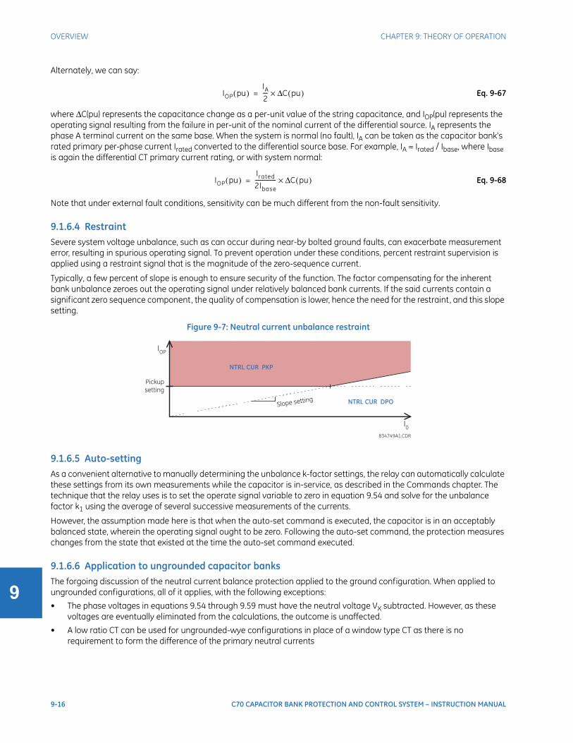
9-16 C70 CAPACITOR BANK PROTECTION AND CONTROL SYSTEM – INSTRUCTION MANUAL
OVERVIEW CHAPTER 9: THEORY OF OPERATION
9
Alternately, we can say:
Eq. 9-67
where ΔC(pu) represents the capacitance change as a per-unit value of the string capacitance, and IOP(pu) represents the operating signal resulting from the failure in per-unit of the nominal current of the differential source. IA represents the phase A terminal current on the same base. When the system is normal (no fault), IA can be taken as the capacitor bank's rated primary per-phase current Irated converted to the differential source base. For example, IA = Irated / Ibase, where Ibase is again the differential CT primary current rating, or with system normal:
Eq. 9-68
Note that under external fault conditions, sensitivity can be much different from the non-fault sensitivity.
9.1.6.4 RestraintSevere system voltage unbalance, such as can occur during near-by bolted ground faults, can exacerbate measurement error, resulting in spurious operating signal. To prevent operation under these conditions, percent restraint supervision is applied using a restraint signal that is the magnitude of the zero-sequence current.
Typically, a few percent of slope is enough to ensure security of the function. The factor compensating for the inherent bank unbalance zeroes out the operating signal under relatively balanced bank currents. If the said currents contain a significant zero sequence component, the quality of compensation is lower, hence the need for the restraint, and this slope setting.
Figure 9-7: Neutral current unbalance restraint
9.1.6.5 Auto-settingAs a convenient alternative to manually determining the unbalance k-factor settings, the relay can automatically calculate these settings from its own measurements while the capacitor is in-service, as described in the Commands chapter. The technique that the relay uses is to set the operate signal variable to zero in equation 9.54 and solve for the unbalance factor k1 using the average of several successive measurements of the currents.
However, the assumption made here is that when the auto-set command is executed, the capacitor is in an acceptably balanced state, wherein the operating signal ought to be zero. Following the auto-set command, the protection measures changes from the state that existed at the time the auto-set command executed.
9.1.6.6 Application to ungrounded capacitor banksThe forgoing discussion of the neutral current balance protection applied to the ground configuration. When applied to ungrounded configurations, all of it applies, with the following exceptions:
• The phase voltages in equations 9.54 through 9.59 must have the neutral voltage VX subtracted. However, as these voltages are eventually eliminated from the calculations, the outcome is unaffected.
• A low ratio CT can be used for ungrounded-wye configurations in place of a window type CT as there is no requirement to form the difference of the primary neutral currents
IOP pu( )IA
2--- C pu( )Δ×=
IOP pu( )Irated
2Ibase-------------- C pu( )Δ×=
834749A1.CDR
I0
IOP
NTRL CUR PKP
Slope setting
Pickup
setting
NTRL CUR DPO
CHAPTER 9: THEORY OF OPERATION OVERVIEW
C70 CAPACITOR BANK PROTECTION AND CONTROL SYSTEM – INSTRUCTION MANUAL 9-17
9
• Whereas with the grounded configuration IDIF = IN1 – IN2, with the ungrounded configuration IDIF = IN1 = –IN2. This results in the –CA2, –CB2, and –CC2 terms disappearing from equations 9.58 through 9.65. This results in the following changes.
Equation 9.64 becomes:
Eq. 9-69
Equation 9.65 becomes:
Eq. 9-70
Equation 9.67 becomes:
Eq. 9-71
Equation 9.68 becomes:
Eq. 9-72
Note that in the ungrounded case, the operating signal is half of that for the grounded case.
• With the grounded configuration, the two banks must be nominally identical. With the ungrounded configuration the two banks need not be the identical though each ideally are balanced. In this situation, the base for ΔC(pu) is the capacitance of the string that has the element failure, so the larger bank has a lower sensitivity than the smaller bank.
k1 kA a2kB akC+ +=
CA1
CA1 CA2+---------------------- a
2 CB1
CB1 CB2+---------------------- a
CC1
CC1 CC2+----------------------+ +=
ddCA1-----------IOP
CA1 CA2+( ) CA1–
CA1 CA2+( )2----------------------------------------IA=
CA2IA
CA1 CA2+( )2-----------------------------=
IA
4--- 1
CA1--------×≅
IOP pu( )IA
4--- C pu( )Δ×=
IOP pu( )Irated
4Ibase-------------- C pu( )Δ×=

9-18 C70 CAPACITOR BANK PROTECTION AND CONTROL SYSTEM – INSTRUCTION MANUAL
OVERVIEW CHAPTER 9: THEORY OF OPERATION
9

C70 CAPACITOR BANK PROTECTION AND CONTROL SYSTEM – INSTRUCTION MANUAL 10-1
C70 Capacitor Bank Protection and Control System
Chapter 10: Maintenance
Maintenance
This chapter outlines maintenance, repair, storage, and disposal of the hardware and software.
10.1 General maintenanceThe C70 requires minimal maintenance. As a microprocessor-based relay, its characteristics do not change over time. Expected service life is 20 years for UR devices manufactured June 2014 or later when applied in a controlled indoors environment and electrical conditions within specification.
While the C70 performs continual self-tests, it is recommended that maintenance be scheduled with other system maintenance. This maintenance can involve in-service, out-of-service, or unscheduled maintenance.
10.1.1 In-service maintenance1. Visual verification of the analog values integrity, such as voltage and current (in comparison to other devices on the
corresponding system).
2. Visual verification of active alarms, relay display messages, and LED indications.
3. LED test.
4. Visual inspection for any damage, corrosion, dust, or loose wires.
5. Event recorder file download with further events analysis.
10.1.2 Out-of-service maintenance1. Check wiring connections for firmness.
2. Analog values (currents, voltages, RTDs, analog inputs) injection test and metering accuracy verification. Calibrated test equipment is required.
3. Protection elements setting verification (analog values injection or visual verification of setting file entries against relay settings schedule).
4. Contact inputs and outputs verification. This test can be conducted by direct change of state forcing or as part of the system functional testing.
5. Visual inspection for any damage, corrosion, or dust.
6. Event recorder file download with further events analysis.
7. LED Test and pushbutton continuity check.

10-2 C70 CAPACITOR BANK PROTECTION AND CONTROL SYSTEM – INSTRUCTION MANUAL
BACK UP AND RESTORE SETTINGS CHAPTER 10: MAINTENANCE
10
10.1.3 Unscheduled maintenance (system interruption)1. View the event recorder and oscillography or fault report for correct operation of inputs, outputs, and elements.
10.2 Back up and restore settingsBack up a copy of the in-service settings for each commissioned UR device, so as to revert to the commissioned settings after inadvertent, unauthorized, or temporary setting changes are made, after the settings defaulted due to firmware upgrade, or when the device has to be replaced. This section describes how to backup settings to a file and how to use that file to restore the settings to the original relay or to a replacement relay.
10.2.1 Back up settingsUR device settings can be saved in a backup URS file using the EnerVista UR Setup software. The URS file is the standard UR settings file. For an introduction to settings files in the URS format, see the beginning of the Interfaces chapter. When the IEC 61850 option is present, the settings can alternatively be saved in a backup IID file either using the EnerVista UR Setup software in online mode or by using any of the supported file transfer protocols. The IID file is an IEC 61850 Substation Configuration Language (SCL) file; see the IEC 61850 chapter in the UR Series Communications Guide for an introduction to SCL.
The options that display in the EnerVista software when right-clicking depend on device options.
To save a settings file in the URS format:
1. In EnerVista, connect to the device in the Online Window area.
2. Right-click the device name in the Online Window area and select Read Device Settings. A window opens.
3. Select or enter a file name and location, and click the Receive button. A .urs file is created in the Offline Window area.
To save settings in the IID format in EnerVista:
1. In EnerVista, connect to the device in the Online Window area.
2. Right-click the device name in the Online Window area and select Read IID File. The option is not present when the device does not have the IEC 61850 option. A window opens when successful.
3. Select or enter a file name and location, and click the Receive button. A .iid file is created.
To save settings in the IID format using TFTP:
1. On a computer on the same subnetwork as the UR device, open a command window.
2. EnterTFTP <IP address> GET ur.iid <destination>
where
<IP address> is the IP address of the UR deviceur.iid is the internal name of the IID file in the UR device<destination> is the path and file name of the IID file. If omitted, the file is saved as ur.iid in the command window default directory.
An example is TFTP 192.168.1.101 GET ur.iid Feeder1.iid
To avoid deterioration of electrolytic capacitors, power up units that are stored in a de-energized state once per year, for one hour continuously.

CHAPTER 10: MAINTENANCE BACK UP AND RESTORE SETTINGS
C70 CAPACITOR BANK PROTECTION AND CONTROL SYSTEM – INSTRUCTION MANUAL 10-3
10
10.2.2 Restore settingsUR device settings can be restored to the values they were at when a URS backup file was created using the EnerVista UR Setup software. When the IEC 61850 option is present, the settings can alternatively be to the values they were at when an IID type backup was created either using the EnerVista UR Setup software in online mode or by using any of the supported file transfer protocols. Note that TFTP cannot be used here, as TFTP "put" mode is disabled for security reasons.
To restore completely, a few settings need to be entered manually either via EnerVista UR Setup or via the UR device front panel. If the restore operation is to be via Ethernet, first the UR device must have its IP address settings entered via the front panel. These are located at SETTINGS PRODUCT SETUP COMMUNICATIONS NETWORK 1(3) and SETTINGS PRODUCT SETUP COMMUNICATIONS IPv4 ROUTE TABLE 1(6) DEFAULT IPv4 ROUTE GATEWAY ADDRESS.
To restore settings from a URS file:
1. In EnerVista, connect to the device in the Online Window area.
2. Right-click the .urs file in the Offline Window area and select Add Existing Settings File to locate a file, and/or drag-and-drop the file from the Offline Window area to the device in the Online Window area.
Figure 10-1: Restoring a URS settings file
3. Manually copy the remaining settings, outlined as follows.
To restore settings from an IID file using EnerVista software:
1. In Windows, make a copy the IID file with a cid extension.
2. Connect to the device in the Online Window area.
3. In the Offline Window area, right-click Files and select Import Contents From SCD/CID.
Figure 10-2: Importing a CID file
4. Navigate to and select the file with .cid extension. When prompted, enter a file name to give to an intermediate URS file. The URS file is added to the Offline Window area.
5. Drag the imported file in the Offline Window to the device in the Online Window.
6. Manually copy the remaining settings, outlined as follows.
To restore settings from an IID using SFTP:
1. In Windows, make a copy the IID file with a cid extension.
2. On a computer on the same subnetwork as the UR device, open a SFTP client application, such as WinSCP. Note that TFTP cannot be used here.
3. Use the device's IP address as the host name.

10-4 C70 CAPACITOR BANK PROTECTION AND CONTROL SYSTEM – INSTRUCTION MANUAL
UPGRADE FIRMWARE CHAPTER 10: MAINTENANCE
10
4. If the device has the CyberSentry option, use the User Name of "Administrator" or "Engineer", and the password programmed for the selected role. The default password is "ChangeMe1#" (without quotation marks).
5. If the device does not have the CyberSentry option, use the User Name of "Setting", and the password programmed for the Setting role. The default password is "ChangeMe1#" (without quotation marks).
6. Upload the backup file copy with the CID extension. WinSCP uses drag-and-drop or copy-and-paste for this.
7. Manually copy the remaining settings, outlined as follows.
To manually copy remaining settings:
1. Settings listed in section 4.1.2 Settings Files are not transferred to the UR device with settings files. Enter them manually either via the front panel or via EnerVista UR Setup software. The values that these settings had at the time the backup was created are contained within the backup file, accessed through EnerVista UR Setup software.
10.3 Upgrade firmwareThe firmware of the C70 device can be upgraded, locally or remotely, using the EnerVista software. Instructions are outlined here and in the Help file under the topic “Upgrading Firmware.”
Upgrades are possible for the same release (such as 7.01 to 7.02) and from one firmware version to another (such as 7.2 to 7.3). When upgrading to another firmware version, check the release notes for compatibility. Release notes are located in the Support Documents section of the website at http://gedigitalenergy.com/app/ViewFiles.aspx?prod=urfamily&type=9
If you are upgrading from version 7.0 or 7.1 to 7.2 or later, some CPU modules require a new boot version. Update this first.
To upgrade the firmware:
1. If required, download the boot file and/or firmware from http://www.gedigitalenergy.com/app/ViewFiles.aspx?prod=urfamily&type=7 The firmware and boot files are .bin files.
2. Navigate to Settings > Product Setup > Security and ensure that the Remote Setting Authorized and Local Setting Authorized settings are "ON." On the front panel of the device, the path is Settings Product Setup Security Dual Permission Security Access.
If using CyberSentry security, also ensure that the relay and firmware are not locked under the Settings > Product Setup > Security > Supervisory settings.
3. In EnerVista, back up the device settings by right-clicking the device and selecting Read Device Settings. In the window that displays, select an existing file to overwrite, or enter a name for a new settings file and optionally a location for the new file. Click the Receive button to start the backup.
If an "Incompatible device order codes or versions" message displays, it means that you are trying to overwrite a file for another product. You access the Convert Settings File option by right-clicking the file in the Offline Window area at the lower left.
4. In EnerVista, navigate to Maintenance > Update Firmware.
First select the boot file if applicable, locating the .bin file, and proceed. Restart the device, the EnerVista software, and refresh the order code in EnerVista under the Device Setup button.
To update the firmware, click Maintenance > Update Firmware, select the firmware update by locating the .bin file, and proceed with the update.
If an "Unable to put relay in flash mode" message displays, set the Settings > Product Setup > Security > Dual Permission Security Access > Remote Setting Authorized and Local Setting Authorized settings to "ON" and try again.
When the update is finished, restart the device by clicking Maintenance > Reboot Relay Command, restart the EnerVista software, and refresh the order code in EnerVista under the Device Setup button. As the device is starting up, verify the boot and firmware version, or in EnerVista check them under Actual Values > Product Info > Firmware Revisions. The boot version is not the same as the firmware revision, and the firmware revision reflects the UR release, for example firmware revision 7.3 is UR release 7.3.
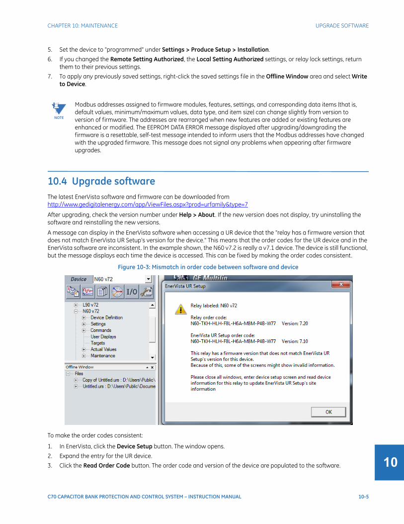
CHAPTER 10: MAINTENANCE UPGRADE SOFTWARE
C70 CAPACITOR BANK PROTECTION AND CONTROL SYSTEM – INSTRUCTION MANUAL 10-5
10
5. Set the device to "programmed" under Settings > Produce Setup > Installation.
6. If you changed the Remote Setting Authorized, the Local Setting Authorized settings, or relay lock settings, return them to their previous settings.
7. To apply any previously saved settings, right-click the saved settings file in the Offline Window area and select Write to Device.
10.4 Upgrade softwareThe latest EnerVista software and firmware can be downloaded from http://www.gedigitalenergy.com/app/ViewFiles.aspx?prod=urfamily&type=7
After upgrading, check the version number under Help > About . If the new version does not display, try uninstalling the software and reinstalling the new versions.
A message can display in the EnerVista software when accessing a UR device that the "relay has a firmware version that does not match EnerVista UR Setup’s version for the device." This means that the order codes for the UR device and in the EnerVista software are inconsistent. In the example shown, the N60 v7.2 is really a v7.1 device. The device is still functional, but the message displays each time the device is accessed. This can be fixed by making the order codes consistent.
Figure 10-3: Mismatch in order code between software and device
To make the order codes consistent:
1. In EnerVista, click the Device Setup button. The window opens.
2. Expand the entry for the UR device.
3. Click the Read Order Code button. The order code and version of the device are populated to the software.
NOTE
Modbus addresses assigned to firmware modules, features, settings, and corresponding data items (that is, default values, minimum/maximum values, data type, and item size) can change slightly from version to version of firmware. The addresses are rearranged when new features are added or existing features are enhanced or modified. The EEPROM DATA ERROR message displayed after upgrading/downgrading the firmware is a resettable, self-test message intended to inform users that the Modbus addresses have changed with the upgraded firmware. This message does not signal any problems when appearing after firmware upgrades.

10-6 C70 CAPACITOR BANK PROTECTION AND CONTROL SYSTEM – INSTRUCTION MANUAL
REPLACE MODULE CHAPTER 10: MAINTENANCE
10
4. Click the OK button to save the change.
10.5 Replace moduleThis section outlines how to replace a module.
The relay, being modular in design, allows for the withdrawal and insertion of modules. Replace modules only with like modules in their original factory configured slots.
To replace a module:
1. Open the enhanced faceplate to the left once the thumb screw has been removed. This allows for easy access of the modules for withdrawal. The new wide-angle hinge assembly in the enhanced front panel opens completely and allows easy access to all modules in the C70.
Figure 10-4: Modules inside relay with front cover open (enhanced faceplate)
The standard faceplate can be opened to the left once the black plastic sliding latch on the right side has been pushed up, as shown below.
Withdraw or insert a module only when control power has been removed from the unit, and be sure to insert only the correct module type into a slot, else personal injury, damage to the unit or connected equipment, or undesired operation can result.
To avoid damage to the equipment, use proper electrostatic discharge protection (for example, a static strap) when coming in contact with modules while the relay is energized.
842812A1.CDR

CHAPTER 10: MAINTENANCE BATTERY
C70 CAPACITOR BANK PROTECTION AND CONTROL SYSTEM – INSTRUCTION MANUAL 10-7
10
Figure 10-5: Removing module (standard faceplate)
2. With power to the unit off, disconnect individually the connections from the module before removing the module from the chassis.
3. To properly remove a module, pull simultaneously the ejector/inserter clips, located at the top and bottom of the module. Record the original location of the module to ensure that the same or replacement module is inserted into the correct slot. Modules with current input provide automatic shorting of external CT circuits.
To properly insert a module, ensure that the correct module type is inserted into the correct slot position. The ejector/inserter clips located at the top and at the bottom of each module must be in the disengaged position as the module is smoothly inserted into the slot. Once the clips have cleared the raised edge of the chassis, engage the clips simultaneously. When the clips have locked into position, the module is fully inserted.
10.6 BatteryA battery powers the real time clock on startup of the device.
When required, the battery can be replaced. Because the power supply module contains the battery and there are two power supply options, two procedures are possible. To determine which procedure to use, check the power supply module or use the photographs here.
10.6.1 Replace battery for RH/RL power supplyWhen required, the battery can be replaced. The power supply module contains the battery.
To replace the battery:
1. Turn off the power to the unit.
2. Wait a minimum of three minutes to ensure that there is no power to the battery.
3. As outlined in the previous section, open the unit by sliding up the plastic latch on the right side of the front panel (standard front panel) or unscrewing the panel (enhanced front panel).
4. For the standard front panel, it needs to be removed in order to access the power supply module, which is typically in the first slot on the left side and blocked by the hinge of the front panel. To remove the front panel, unscrew its bracket
To avoid injury, ensure that the unit has been powered off for a minimum of three minutes before replacing the battery.
Risk of fire if battery is replaced with incorrect type or polarity.

10-8 C70 CAPACITOR BANK PROTECTION AND CONTROL SYSTEM – INSTRUCTION MANUAL
BATTERY CHAPTER 10: MAINTENANCE
10
on the front left side of the unit.
5. Simultaneously pull the ejector clips at the top and bottom of the power supply module and remove the module.
6. Unscrew the screw that attaches the metal cover to the module.
7. Slide the metal cover away from the clips about 1 cm (1/4 inch) and remove the cover.
8. Unclip the black plastic holder that keeps the battery in place. The plastic clips into the socket at the bottom on both sides. Use a flat-head screwdriver if you cannot unclip the plastic with your fingers.
9. Observe the + and - polarity of the battery and replace it with the same polarity as marked on the battery holder. Replace the battery with the identical make and model. For example, do not use a rechargeable battery.
Figure 10-6: Battery location on RH/RL power supply module
10. Reinstall the battery clip and the metal cover, and reinsert the power supply module into the unit.
11. Power on the unit.
12. Dispose of the old battery as outlined in the next section.
10.6.2 Replace battery for SH/SL power supplyWhen required, the battery can be replaced. The power supply module contains the battery.
To replace the battery:
1. Turn off the power to the unit.
2. Wait a minimum of three minutes to ensure that there is no power to the battery.
3. As outlined in the previous section, open the unit by sliding up the plastic latch on the right side of the front panel (standard front panel) or unscrewing the panel (enhanced front panel).
4. For the standard front panel, it needs to be removed in order to access the power supply module, which is typically in the first slot on the left side and blocked by the hinge of the front panel. To remove the front panel, unscrew the bracket on the front left side of the unit.
5. Simultaneously pull the ejector clips at the top and bottom of the power supply module and remove the module.
6. Unscrew all four screws (not three) that attach the metal cover to the module.
7. Slide the metal cover away from the clips about 1 cm (1/4 inch) and remove the cover.
8. Unclip the black plastic holder that keeps the battery in place. The plastic clips into the socket at the bottom on both sides. Use a flat-head screwdriver if you cannot unclip the plastic with your fingers.
To avoid injury, ensure that the unit has been powered off for a minimum of three minutes before replacing the battery.
Risk of fire if battery is replaced with incorrect type or polarity.
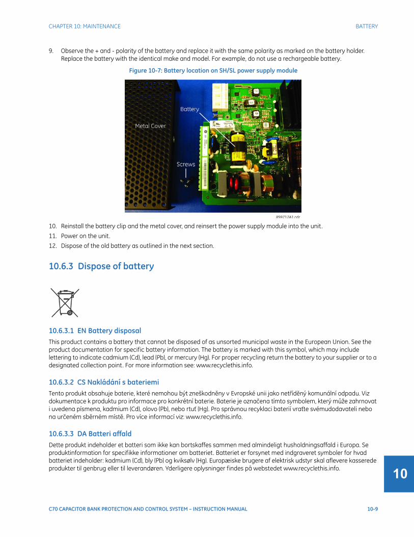
CHAPTER 10: MAINTENANCE BATTERY
C70 CAPACITOR BANK PROTECTION AND CONTROL SYSTEM – INSTRUCTION MANUAL 10-9
10
9. Observe the + and - polarity of the battery and replace it with the same polarity as marked on the battery holder. Replace the battery with the identical make and model. For example, do not use a rechargeable battery.
Figure 10-7: Battery location on SH/SL power supply module
10. Reinstall the battery clip and the metal cover, and reinsert the power supply module into the unit.
11. Power on the unit.
12. Dispose of the old battery as outlined in the next section.
10.6.3 Dispose of battery
10.6.3.1 EN Battery disposalThis product contains a battery that cannot be disposed of as unsorted municipal waste in the European Union. See the product documentation for specific battery information. The battery is marked with this symbol, which may include lettering to indicate cadmium (Cd), lead (Pb), or mercury (Hg). For proper recycling return the battery to your supplier or to a designated collection point. For more information see: www.recyclethis.info.
10.6.3.2 CS Nakládání s bateriemiTento produkt obsahuje baterie, které nemohou být zneškodněny v Evropské unii jako netříděný komunální odpadu. Viz dokumentace k produktu pro informace pro konkrétní baterie. Baterie je označena tímto symbolem, který může zahrnovat i uvedena písmena, kadmium (Cd), olovo (Pb), nebo rtuť (Hg). Pro správnou recyklaci baterií vraťte svémudodavateli nebo na určeném sběrném místě. Pro více informací viz: www.recyclethis.info.
10.6.3.3 DA Batteri affaldDette produkt indeholder et batteri som ikke kan bortskaffes sammen med almindeligt husholdningsaffald i Europa. Se produktinformation for specifikke informationer om batteriet. Batteriet er forsynet med indgraveret symboler for hvad batteriet indeholder: kadmium (Cd), bly (Pb) og kviksølv (Hg). Europæiske brugere af elektrisk udstyr skal aflevere kasserede produkter til genbrug eller til leverandøren. Yderligere oplysninger findes på webstedet www.recyclethis.info.

10-10 C70 CAPACITOR BANK PROTECTION AND CONTROL SYSTEM – INSTRUCTION MANUAL
BATTERY CHAPTER 10: MAINTENANCE
10
10.6.3.4 DE Entsorgung von BatterienDieses Produkt beinhaltet eine Batterie, die nicht als unsortierter städtischer Abfall in der europäischen Union entsorgt werden darf. Beachten Sie die spezifischen Batterie-informationen in der Produktdokumentation. Die Batterie ist mit diesem Symbol gekennzeichnet, welches auch Hinweise auf möglicherweise enthaltene Stoffe wie Kadmium (Cd), Blei (Pb) oder Quecksilber (Hektogramm) darstellt . Für die korrekte Wiederverwertung bringen Sie diese Batterie zu Ihrem lokalen Lieferanten zurück oder entsorgen Sie das Produkt an den gekennzeichneten Sammelstellen. Weitere Informationen hierzu finden Sie auf der folgenden Website: www.recyclethis.info.
10.6.3.5 EL Απόρριψη μπαταριώνΑυτό το προϊόν περιέχει μια μπαταρία που δεν πρέπει να απορρίπτεται σε δημόσια συστήματα απόρριψης στην Ευρωπαϊκή Κοινότητα. ∆είτε την τεκμηρίωση του προϊόντος για συγκεκριμένες πληροφορίες που αφορούν τη μπαταρία. Η μπαταρία είναι φέρει σήμανση με αυτό το σύμβολο, το οποίο μπορεί να περιλαμβάνει γράμματα για να δηλώσουν το κάδμιο (Cd), τον μόλυβδο (Pb), ή τον υδράργυρο (Hg). Για την κατάλληλη ανακύκλωση επιστρέψτε την μπαταρία στον προμηθευτή σας ή σε καθορισμένο σημείο συλλογής. Για περισσότερες πληροφορίες δείτε: www.recyclethis.info.
10.6.3.6 ES Eliminacion de bateriasEste producto contiene una batería que no se pueda eliminar como basura normal sin clasificar en la Unión Europea. Examine la documentación del producto para la información específica de la batería. La batería se marca con este símbolo, que puede incluir siglas para indicar el cadmio (Cd), el plomo (Pb), o el mercurio (Hg ). Para el reciclaje apropiado, devuelva este producto a su distribuidor ó deshágase de él en los puntos de reciclaje designados. Para mas información : wwwrecyclethis.info.
10.6.3.7 ET Patareide kõrvaldamineKäesolev toode sisaldab patareisid, mida Euroopa Liidus ei tohi kõrvaldada sorteerimata olmejäätmetena. Andmeid patareide kohta vaadake toote dokumentatsioonist. Patareid on märgistatud käesoleva sümboliga, millel võib olla kaadmiumi (Cd), pliid (Pb) või elavhõbedat (Hg) tähistavad tähed. Nõuetekohaseks ringlusse võtmiseks tagastage patarei tarnijale või kindlaksmääratud vastuvõtupunkti. Lisainformatsiooni saab Internetist aadressil: www.recyclethis.info.
10.6.3.8 FI Paristoje ja akkujen hävittäminenTuote sisältää pariston, jota ei saa hävittää Euroopan Unionin alueella talousjätteen mukana. Tarkista tuoteselosteesta tuotteen tiedot. Paristo on merkitty tällä symbolilla ja saattaa sisältää cadmiumia (Cd), lyijyä (Pb) tai elohopeaa (Hg). Oikean kierrätystavan varmistamiseksi palauta tuote paikalliselle jälleenmyyjälle tai palauta se paristojen keräyspisteeseen. Lisätietoja sivuilla www.recyclethis.info.
10.6.3.9 FR Élimination des pilesCe produit contient une batterie qui ne peuvent être éliminés comme déchets municipaux non triés dans l'Union européenne. Voir la documentation du produit au niveau des renseignements sur la pile. La batterie est marqué de ce symbole, qui comprennent les indications cadmium (Cd), plomb (Pb), ou mercure (Hg). Pour le recyclage, retourner la batterie à votre fournisseur ou à un point de collecte. Pour plus d'informations, voir: www.recyclethis.info.
10.6.3.10 HU Akkumulátor hulladék kezeléseEzen termék akkumulátort tartalmaz, amely az Európai Unión belül csak a kijelölt módon és helyen dobható ki. A terméken illetve a mellékelt ismertetőn olvasható a kadmium (Cd), ólom (Pb) vagy higany (Hg) tartalomra utaló betűjelzés. A hulladék akkumulátor leadható a termék forgalmazójánál új akkumulátor vásárlásakor, vagy a kijelölt elektronikai hulladékudvarokban. További információ a www.recyclethis.info oldalon.

CHAPTER 10: MAINTENANCE BATTERY
C70 CAPACITOR BANK PROTECTION AND CONTROL SYSTEM – INSTRUCTION MANUAL 10-11
10
10.6.3.11 IT Smaltimento batterieQuesto prodotto contiene una batteria che non può essere smaltita nei comuni contenitori per lo smaltimento rifiuti, nell' Unione Europea. Controllate la documentazione del prodotto per le informazioni specifiche sulla batteria. La batteria è contrassegnata con questo simbolo e può includere alcuni caratteri ad indicare la presenza di cadmio (Cd), piombo (Pb) oppure mercurio (Hg). Per il corretto smaltimento, potete restituirli al vostro fornitore locale, oppure rivolgervi e consegnarli presso i centri di raccolta preposti. Per maggiori informazioni vedere: ww.recyclethis.info.
10.6.3.12 LT Baterijų šalinimasŠios įrangos sudėtyje yra baterijų, kurias draudžiama šalinti Europos Sąjungos viešose nerūšiuotų atliekų šalinimo sistemose. Informaciją apie baterijas galite rasti įrangos techninėje dokumentacijoje. Baterijos žymimos šiuo simboliu, papildomai gali būti nurodoma kad baterijų sudėtyje yra kadmio (Cd), švino (Pb) ar gyvsidabrio (Hg). Eksploatavimui nebetinkamas baterijas pristatykite į tam skirtas surinkimo vietas arba grąžinkite jas tiesioginiam tiekėjui, kad jos būtų tinkamai utilizuotos. Daugiau informacijos rasite šioje interneto svetainėje: www.recyclethis.info.
10.6.3.13 LV Bateriju likvidēšanaŠis produkts satur bateriju vai akumulatoru, kuru nedrīkst izmest Eiropas Savienībā esošajās sadzīves atkritumu sistēmās. Sk. produkta dokumentācijā, kur ir norādīta konkrēta informācija par bateriju vai akumulatoru. Baterijas vai akumulatora marķējumā ir šis simbols, kas var ietvert burtus, kuri norāda kadmiju (Cd), svinu (Pb) vai dzīvsudrabu (Hg). Pēc ekspluatācijas laika beigām baterijas vai akumulatori jānodod piegādātājam vai specializētā bateriju savākšanas vietā. Sīkāku informāciju var iegūt vietnē: www.recyclethis.info.
10.6.3.14 NL Verwijderen van baterijenDit product bevat een batterij welke niet kan verwijdert worden via de gemeentelijke huisvuilscheiding in de Europese Gemeenschap. Gelieve de product documentatie te controleren voor specifieke batterij informatie. De batterijen met deze label kunnen volgende indictaies bevatten cadium (Cd), lood (Pb) of kwik (Hg). Voor correcte vorm van kringloop, geef je de producten terug aan jou locale leverancier of geef het af aan een gespecialiseerde verzamelpunt. Meer informatie vindt u op de volgende website: www.recyclethis.info.
10.6.3.15 NO Retur av batteriDette produkt inneholder et batteri som ikke kan kastes med usortert kommunalt søppel i den Europeiske Unionen. Se produktdokumentasjonen for spesifikk batteriinformasjon. Batteriet er merket med dette symbolet som kan inkludere symboler for å indikere at kadmium (Cd), bly (Pb), eller kvikksølv (Hg) forekommer. Returner batteriet til leverandøren din eller til et dedikert oppsamlingspunkt for korrekt gjenvinning. For mer informasjon se: www.recyclethis.info.
10.6.3.16 PL Pozbywanie się zużytych bateriiTen produkt zawiera baterie, które w Unii Europejskiej mogą być usuwane tylko jako posegregowane odpady komunalne. Dokładne informacje dotyczące użytych baterii znajdują się w dokumentacji produktu. Baterie oznaczone tym symbolem mogą zawierać dodatkowe oznaczenia literowe wskazujące na zawartość kadmu (Cd), ołowiu (Pb) lub rtęci (Hg). Dla zapewnienia właściwej utylizacji, należy zwrócić baterie do dostawcy albo do wyznaczonego punktu zbiórki. Więcej informacji można znaleźć na stronie internetowej www.recyclethis.info.
10.6.3.17 PT Eliminação de BateriasEste produto contêm uma bateria que não pode ser considerado lixo municipal na União Europeia. Consulte a documentação do produto para obter informação específica da bateria. A bateria é identificada por meio de este símbolo, que pode incluir a rotulação para indicar o cádmio (Cd), chumbo (Pb), ou o mercúrio (hg). Para uma reciclagem apropriada envie a bateria para o seu fornecedor ou para um ponto de recolha designado. Para mais informação veja: www.recyclethis.info.
10-12 C70 CAPACITOR BANK PROTECTION AND CONTROL SYSTEM – INSTRUCTION MANUAL
CLEAR FILES AND DATA AFTER UNINSTALL CHAPTER 10: MAINTENANCE
10
10.6.3.18 RU Утилизация батарейСогласно европейской директиве об отходах электрического и электронного оборудования, продукты, содержащие батареи, нельзя утилизировать как обычные отходы на территории ЕС. Более подробную информацию вы найдете в документации к продукту. На этом символе могут присутствовать буквы, которые означают, что батарея собержит кадмий (Cd), свинец (Pb) или ртуть (Hg). Для надлежащей утилизации по окончании срока эксплуатации пользователь должен возвратить батареи локальному поставщику или сдать в специальный пункт приема. Подробности можно найти на веб-сайте: www.recyclethis.info.
10.6.3.19 SK Zaobchádzanie s batériamiTento produkt obsahuje batériu, s ktorou sa v Európskej únii nesmie nakladať ako s netriedeným komunálnym odpadom. Dokumentácia k produktu obsahuje špecifické informácie o batérii. Batéria je označená týmto symbolom, ktorý môže obsahovať písmená na označenie kadmia (Cd), olova (Pb), alebo ortuti (Hg). Na správnu recykláciu vráťte batériu vášmu lokálnemu dodávateľovi alebo na určené zberné miesto. Pre viac informácii pozrite: www.recyclethis.info.
10.6.3.20 SL Odlaganje baterijTa izdelek vsebuje baterijo, ki je v Evropski uniji ni dovoljeno odstranjevati kot nesortiran komunalni odpadek. Za posebne informacije o bateriji glejte dokumentacijo izdelka. Baterija je označena s tem simbolom, ki lahko vključuje napise, ki označujejo kadmij (Cd), svinec (Pb) ali živo srebro (Hg). Za ustrezno recikliranje baterijo vrnite dobavitelju ali jo odstranite na določenem zbirališču. Za več informacij obiščite spletno stran: www.recyclethis.info.
10.6.3.21 SV Kassering av batteriDenna produkt innehåller ett batteri som inte får kastas i allmänna sophanteringssytem inom den europeiska unionen. Se produktdokumentationen för specifik batteriinformation. Batteriet är märkt med denna symbol, vilket kan innebära att det innehåller kadmium (Cd), bly (Pb) eller kvicksilver (Hg). För korrekt återvinning skall batteriet returneras till leverantören eller till en därför avsedd deponering. För mer information, se: www.recyclethis.info.
10.6.3.22 TR Pil Geri DönüşümüBu ürün Avrupa Birliği genel atık sistemlerine atılmaması gereken pil içermektedir. Daha detaylı pil bilgisi için ürünün kataloğunu inceleyiniz. Bu sembolle işaretlenmiş piller Kadmiyum(Cd), Kurşun(Pb) ya da Civa(Hg) içerebilir. Doğru geri dönüşüm için ürünü yerel tedarikçinize geri veriniz ya da özel işaretlenmiş toplama noktlarına atınız. Daha fazla bilgi için: www.recyclethis.info.
10.6.3.23 Global contacts
From GE Part Number 1604-0021-A1, GE Publication Number GEK-113574
10.7 Clear files and data after uninstallThe unit can be decommissioned by turning off power to the unit and disconnecting the wires to it .
Files can be cleared after uninstalling the EnerVista software or UR device, for example to comply with data security regulations.
On the computer, settings files can identified by the .urs extension. To clear the current settings file, create a default settings file, write it to the relay, then delete all other .urs files. For the existing installation, upgrading the firmware overwrites the flash memory. Other files can be in standard formats, such as COMTRADE or .csv.
North America 905-294-6222
Latin America +55 11 3614 1700
Europe, Middle East, Africa +(34) 94 485 88 00
Asia +86-21-2401-3208
India +91 80 41314617
CHAPTER 10: MAINTENANCE REPAIRS
C70 CAPACITOR BANK PROTECTION AND CONTROL SYSTEM – INSTRUCTION MANUAL 10-13
10
You cannot erase directly the flash memory, but all records and settings in that memory can be deleted. Do this using the SETTINGS PRODUCT SETUP CLEAR RELAY RECORDS command.
10.8 RepairsThe battery and modules inside the case can be replaced without return of the device to the factory. The firmware and software can be upgraded without return of the device to the factory.
For issues not solved by troubleshooting, the process to return the device to the factory for repair is as follows:
• Contact a GE Digital Energy Technical Support Center. Contact information is found in the first chapter.
• Obtain a Return Materials Authorization (RMA) number from the Technical Support Center.
• Verify that the RMA and Commercial Invoice received have the correct information.
• Tightly pack the unit in a box with bubble wrap, foam material, or styrofoam inserts or packaging peanuts to cushion the item(s). You may also use double boxing whereby you place the box in a larger box that contains at least 5 cm of cushioning material.
• Ship the unit by courier or freight forwarder, along with the Commercial Invoice and RMA, to the factory.
GE DIGITAL ENERGY
650 MARKLAND STREET
MARKHAM, ONTARIO
CANADA L6C 0M1
ATTN: SERVICE DEPT.
RMA# : ______________
Customers are responsible for shipping costs to the factory, regardless of whether the unit is under warranty.
• Fax a copy of the shipping information to the GE Digital Energy service department in Canada at +1 905 927 5098.
Use the detailed return procedure outlined at
https://www.gedigitalenergy.com/multilin/support/ret_proc.htm
The current warranty and return information are outlined at
https://www.gedigitalenergy.com/multilin/warranty.htm
10.9 StorageStore the unit indoors in a cool, dry place. If possible, store in the original packaging. Follow the storage temperature range outlined in the Specifications.
10.10 DisposalOther than the battery, there are no special requirements for disposal of the unit at the end its service life. For customers located in the European Union, dispose of the battery as outlined earlier. To prevent non-intended use of the unit, remove the modules as outlined earlier, dismantle the unit, and recycle the metal when possible.
To avoid deterioration of electrolytic capacitors, power up units that are stored in a de-energized state once per year, for one hour continuously.

10-14 C70 CAPACITOR BANK PROTECTION AND CONTROL SYSTEM – INSTRUCTION MANUAL
DISPOSAL CHAPTER 10: MAINTENANCE
10

C70 CAPACITOR BANK PROTECTION AND CONTROL SYSTEM – INSTRUCTION MANUAL A-1
C70 Capacitor Bank Protection and Control System
Appendix A: FlexAnalog operands
AppendicesFlexAnalog operands
This appendix outlines FlexAnalog parameters.
A.1 FlexAnalog itemsA FlexAnalog parameter is an analog parameter.
FlexAnalog items are also viewable in a web browser. Enter the IP address of the UR, access the Device Information Menu option, then the FlexAnalog Parameter Listing option. Entries displayed online depend on order code.
Table A-1: FlexAnalog data items
Address FlexAnalog name Units Description
5824 Field RTD 1 Value --- Field RTD 1 value
5825 Field RTD 2 Value --- Field RTD 2 value
5826 Field RTD 3 Value --- Field RTD 3 value
5827 Field RTD 4 Value --- Field RTD 4 value
5828 Field RTD 5 Value --- Field RTD 5 value
5829 Field RTD 6 Value --- Field RTD 6 value
5830 Field RTD 7 Value --- Field RTD 7 value
5831 Field RTD 8 Value --- Field RTD 8 value
5832 Field TDR 1 Value --- Field TDR 1 value
5834 Field TDR 2 Value --- Field TDR 2 value
5836 Field TDR 3 Value --- Field TDR 3 value
5838 Field TDR 4 Value --- Field TDR 4 value
5840 Field TDR 5 Value --- Field TDR 5 value
5842 Field TDR 6 Value --- Field TDR 6 value
5844 Field TDR 7 Value --- Field TDR 7 value
5846 Field TDR 8 Value --- Field TDR 8 value
6144 SRC 1 Ia RMS Amps Source 1 phase A current RMS
6146 SRC 1 Ib RMS Amps Source 1 phase B current RMS
6148 SRC 1 Ic RMS Amps Source 1 phase C current RMS
6150 SRC 1 In RMS Amps Source 1 neutral current RMS
6152 SRC 1 Ia Mag Amps Source 1 phase A current magnitude

A-2 C70 CAPACITOR BANK PROTECTION AND CONTROL SYSTEM – INSTRUCTION MANUAL
FLEXANALOG ITEMS APPENDIX A: FLEXANALOG OPERANDS
A 6154 SRC 1 Ia Angle Degrees Source 1 phase A current angle
6155 SRC 1 Ib Mag Amps Source 1 phase B current magnitude
6157 SRC 1 Ib Angle Degrees Source 1 phase B current angle
6158 SRC 1 Ic Mag Amps Source 1 phase C current magnitude
6160 SRC 1 Ic Angle Degrees Source 1 phase C current angle
6161 SRC 1 In Mag Amps Source 1 neutral current magnitude
6163 SRC 1 In Angle Degrees Source 1 neutral current angle
6164 SRC 1 Ig RMS Amps Source 1 ground current RMS
6166 SRC 1 Ig Mag Amps Source 1 ground current magnitude
6168 SRC 1 Ig Angle Degrees Source 1 ground current angle
6169 SRC 1 I_0 Mag Amps Source 1 zero-sequence current magnitude
6171 SRC 1 I_0 Angle Degrees Source 1 zero-sequence current angle
6172 SRC 1 I_1 Mag Amps Source 1 positive-sequence current magnitude
6174 SRC 1 I_1 Angle Degrees Source 1 positive-sequence current angle
6175 SRC 1 I_2 Mag Amps Source 1 negative-sequence current magnitude
6177 SRC 1 I_2 Angle Degrees Source 1 negative-sequence current angle
6178 SRC 1 Igd Mag Amps Source 1 differential ground current magnitude
6180 SRC 1 Igd Angle Degrees Source 1 differential ground current angle
6208 SRC 2 Ia RMS Amps Source 2 phase A current RMS
6210 SRC 2 Ib RMS Amps Source 2 phase B current RMS
6212 SRC 2 Ic RMS Amps Source 2 phase C current RMS
6214 SRC 2 In RMS Amps Source 2 neutral current RMS
6216 SRC 2 Ia Mag Amps Source 2 phase A current magnitude
6218 SRC 2 Ia Angle Degrees Source 2 phase A current angle
6219 SRC 2 Ib Mag Amps Source 2 phase B current magnitude
6221 SRC 2 Ib Angle Degrees Source 2 phase B current angle
6222 SRC 2 Ic Mag Amps Source 2 phase C current magnitude
6224 SRC 2 Ic Angle Degrees Source 2 phase C current angle
6225 SRC 2 In Mag Amps Source 2 neutral current magnitude
6227 SRC 2 In Angle Degrees Source 2 neutral current angle
6228 SRC 2 Ig RMS Amps Source 2 ground current RMS
6230 SRC 2 Ig Mag Amps Source 2 ground current magnitude
6232 SRC 2 Ig Angle Degrees Source 2 ground current angle
6233 SRC 2 I_0 Mag Amps Source 2 zero-sequence current magnitude
6235 SRC 2 I_0 Angle Degrees Source 2 zero-sequence current angle
6236 SRC 2 I_1 Mag Amps Source 2 positive-sequence current magnitude
6238 SRC 2 I_1 Angle Degrees Source 2 positive-sequence current angle
6239 SRC 2 I_2 Mag Amps Source 2 negative-sequence current magnitude
6241 SRC 2 I_2 Angle Degrees Source 2 negative-sequence current angle
6242 SRC 2 Igd Mag Amps Source 2 differential ground current magnitude
6244 SRC 2 Igd Angle Degrees Source 2 differential ground current angle
6272 SRC 3 Ia RMS Amps Source 3 phase A current RMS
6274 SRC 3 Ib RMS Amps Source 3 phase B current RMS
6276 SRC 3 Ic RMS Amps Source 3 phase C current RMS
6278 SRC 3 In RMS Amps Source 3 neutral current RMS
6280 SRC 3 Ia Mag Amps Source 3 phase A current magnitude
6282 SRC 3 Ia Angle Degrees Source 3 phase A current angle
Address FlexAnalog name Units Description
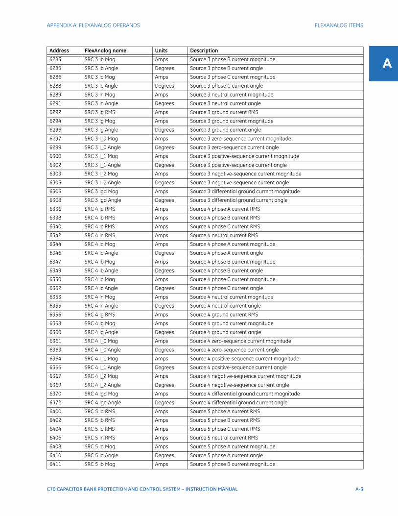
APPENDIX A: FLEXANALOG OPERANDS FLEXANALOG ITEMS
C70 CAPACITOR BANK PROTECTION AND CONTROL SYSTEM – INSTRUCTION MANUAL A-3
A6283 SRC 3 Ib Mag Amps Source 3 phase B current magnitude
6285 SRC 3 Ib Angle Degrees Source 3 phase B current angle
6286 SRC 3 Ic Mag Amps Source 3 phase C current magnitude
6288 SRC 3 Ic Angle Degrees Source 3 phase C current angle
6289 SRC 3 In Mag Amps Source 3 neutral current magnitude
6291 SRC 3 In Angle Degrees Source 3 neutral current angle
6292 SRC 3 Ig RMS Amps Source 3 ground current RMS
6294 SRC 3 Ig Mag Amps Source 3 ground current magnitude
6296 SRC 3 Ig Angle Degrees Source 3 ground current angle
6297 SRC 3 I_0 Mag Amps Source 3 zero-sequence current magnitude
6299 SRC 3 I_0 Angle Degrees Source 3 zero-sequence current angle
6300 SRC 3 I_1 Mag Amps Source 3 positive-sequence current magnitude
6302 SRC 3 I_1 Angle Degrees Source 3 positive-sequence current angle
6303 SRC 3 I_2 Mag Amps Source 3 negative-sequence current magnitude
6305 SRC 3 I_2 Angle Degrees Source 3 negative-sequence current angle
6306 SRC 3 Igd Mag Amps Source 3 differential ground current magnitude
6308 SRC 3 Igd Angle Degrees Source 3 differential ground current angle
6336 SRC 4 Ia RMS Amps Source 4 phase A current RMS
6338 SRC 4 Ib RMS Amps Source 4 phase B current RMS
6340 SRC 4 Ic RMS Amps Source 4 phase C current RMS
6342 SRC 4 In RMS Amps Source 4 neutral current RMS
6344 SRC 4 Ia Mag Amps Source 4 phase A current magnitude
6346 SRC 4 Ia Angle Degrees Source 4 phase A current angle
6347 SRC 4 Ib Mag Amps Source 4 phase B current magnitude
6349 SRC 4 Ib Angle Degrees Source 4 phase B current angle
6350 SRC 4 Ic Mag Amps Source 4 phase C current magnitude
6352 SRC 4 Ic Angle Degrees Source 4 phase C current angle
6353 SRC 4 In Mag Amps Source 4 neutral current magnitude
6355 SRC 4 In Angle Degrees Source 4 neutral current angle
6356 SRC 4 Ig RMS Amps Source 4 ground current RMS
6358 SRC 4 Ig Mag Amps Source 4 ground current magnitude
6360 SRC 4 Ig Angle Degrees Source 4 ground current angle
6361 SRC 4 I_0 Mag Amps Source 4 zero-sequence current magnitude
6363 SRC 4 I_0 Angle Degrees Source 4 zero-sequence current angle
6364 SRC 4 I_1 Mag Amps Source 4 positive-sequence current magnitude
6366 SRC 4 I_1 Angle Degrees Source 4 positive-sequence current angle
6367 SRC 4 I_2 Mag Amps Source 4 negative-sequence current magnitude
6369 SRC 4 I_2 Angle Degrees Source 4 negative-sequence current angle
6370 SRC 4 Igd Mag Amps Source 4 differential ground current magnitude
6372 SRC 4 Igd Angle Degrees Source 4 differential ground current angle
6400 SRC 5 Ia RMS Amps Source 5 phase A current RMS
6402 SRC 5 Ib RMS Amps Source 5 phase B current RMS
6404 SRC 5 Ic RMS Amps Source 5 phase C current RMS
6406 SRC 5 In RMS Amps Source 5 neutral current RMS
6408 SRC 5 Ia Mag Amps Source 5 phase A current magnitude
6410 SRC 5 Ia Angle Degrees Source 5 phase A current angle
6411 SRC 5 Ib Mag Amps Source 5 phase B current magnitude
Address FlexAnalog name Units Description

A-4 C70 CAPACITOR BANK PROTECTION AND CONTROL SYSTEM – INSTRUCTION MANUAL
FLEXANALOG ITEMS APPENDIX A: FLEXANALOG OPERANDS
A 6413 SRC 5 Ib Angle Degrees Source 5 phase B current angle
6414 SRC 5 Ic Mag Amps Source 5 phase C current magnitude
6416 SRC 5 Ic Angle Degrees Source 5 phase C current angle
6417 SRC 5 In Mag Amps Source 5 neutral current magnitude
6419 SRC 5 In Angle Degrees Source 5 neutral current angle
6420 SRC 5 Ig RMS Amps Source 5 ground current RMS
6422 SRC 5 Ig Mag Amps Source 5 ground current magnitude
6424 SRC 5 Ig Angle Degrees Source 5 ground current angle
6425 SRC 5 I_0 Mag Amps Source 5 zero-sequence current magnitude
6427 SRC 5 I_0 Angle Degrees Source 5 zero-sequence current angle
6428 SRC 5 I_1 Mag Amps Source 5 positive-sequence current magnitude
6430 SRC 5 I_1 Angle Degrees Source 5 positive-sequence current angle
6431 SRC 5 I_2 Mag Amps Source 5 negative-sequence current magnitude
6433 SRC 5 I_2 Angle Degrees Source 5 negative-sequence current angle
6434 SRC 5 Igd Mag Amps Source 5 differential ground current magnitude
6436 SRC 5 Igd Angle Degrees Source 5 differential ground current angle
6464 SRC 6 Ia RMS Amps Source 6 phase A current RMS
6466 SRC 6 Ib RMS Amps Source 6 phase B current RMS
6468 SRC 6 Ic RMS Amps Source 6 phase C current RMS
6470 SRC 6 In RMS Amps Source 6 neutral current RMS
6472 SRC 6 Ia Mag Amps Source 6 phase A current magnitude
6474 SRC 6 Ia Angle Degrees Source 6 phase A current angle
6475 SRC 6 Ib Mag Amps Source 6 phase B current magnitude
6477 SRC 6 Ib Angle Degrees Source 6 phase B current angle
6478 SRC 6 Ic Mag Amps Source 6 phase C current magnitude
6480 SRC 6 Ic Angle Degrees Source 6 phase C current angle
6481 SRC 6 In Mag Amps Source 6 neutral current magnitude
6483 SRC 6 In Angle Degrees Source 6 neutral current angle
6484 SRC 6 Ig RMS Amps Source 6 ground current RMS
6486 SRC 6 Ig Mag Amps Source 6 ground current magnitude
6488 SRC 6 Ig Angle Degrees Source 6 ground current angle
6489 SRC 6 I_0 Mag Amps Source 6 zero-sequence current magnitude
6491 SRC 6 I_0 Angle Degrees Source 6 zero-sequence current angle
6492 SRC 6 I_1 Mag Amps Source 6 positive-sequence current magnitude
6494 SRC 6 I_1 Angle Degrees Source 6 positive-sequence current angle
6495 SRC 6 I_2 Mag Amps Source 6 negative-sequence current magnitude
6497 SRC 6 I_2 Angle Degrees Source 6 negative-sequence current angle
6498 SRC 6 Igd Mag Amps Source 6 differential ground current magnitude
6500 SRC 6 Igd Angle Degrees Source 6 differential ground current angle
6656 SRC 1 Vag RMS Volts Source 1 phase AG voltage RMS
6658 SRC 1 Vbg RMS Volts Source 1 phase BG voltage RMS
6660 SRC 1 Vcg RMS Volts Source 1 phase CG voltage RMS
6662 SRC 1 Vag Mag Volts Source 1 phase AG voltage magnitude
6664 SRC 1 Vag Angle Degrees Source 1 phase AG voltage angle
6665 SRC 1 Vbg Mag Volts Source 1 phase BG voltage magnitude
6667 SRC 1 Vbg Angle Degrees Source 1 phase BG voltage angle
6668 SRC 1 Vcg Mag Volts Source 1 phase CG voltage magnitude
Address FlexAnalog name Units Description

APPENDIX A: FLEXANALOG OPERANDS FLEXANALOG ITEMS
C70 CAPACITOR BANK PROTECTION AND CONTROL SYSTEM – INSTRUCTION MANUAL A-5
A6670 SRC 1 Vcg Angle Degrees Source 1 phase CG voltage angle
6671 SRC 1 Vab RMS Volts Source 1 phase AB voltage RMS
6673 SRC 1 Vbc RMS Volts Source 1 phase BC voltage RMS
6675 SRC 1 Vca RMS Volts Source 1 phase CA voltage RMS
6677 SRC 1 Vab Mag Volts Source 1 phase AB voltage magnitude
6679 SRC 1 Vab Angle Degrees Source 1 phase AB voltage angle
6680 SRC 1 Vbc Mag Volts Source 1 phase BC voltage magnitude
6682 SRC 1 Vbc Angle Degrees Source 1 phase BC voltage angle
6683 SRC 1 Vca Mag Volts Source 1 phase CA voltage magnitude
6685 SRC 1 Vca Angle Degrees Source 1 phase CA voltage angle
6686 SRC 1 Vx RMS Volts Source 1 auxiliary voltage RMS
6688 SRC 1 Vx Mag Volts Source 1 auxiliary voltage magnitude
6690 SRC 1 Vx Angle Degrees Source 1 auxiliary voltage angle
6691 SRC 1 V_0 Mag Volts Source 1 zero-sequence voltage magnitude
6693 SRC 1 V_0 Angle Degrees Source 1 zero-sequence voltage angle
6694 SRC 1 V_1 Mag Volts Source 1 positive-sequence voltage magnitude
6696 SRC 1 V_1 Angle Degrees Source 1 positive-sequence voltage angle
6697 SRC 1 V_2 Mag Volts Source 1 negative-sequence voltage magnitude
6699 SRC 1 V_2 Angle Degrees Source 1 negative-sequence voltage angle
6720 SRC 2 Vag RMS Volts Source 2 phase AG voltage RMS
6722 SRC 2 Vbg RMS Volts Source 2 phase BG voltage RMS
6724 SRC 2 Vcg RMS Volts Source 2 phase CG voltage RMS
6726 SRC 2 Vag Mag Volts Source 2 phase AG voltage magnitude
6728 SRC 2 Vag Angle Degrees Source 2 phase AG voltage angle
6729 SRC 2 Vbg Mag Volts Source 2 phase BG voltage magnitude
6731 SRC 2 Vbg Angle Degrees Source 2 phase BG voltage angle
6732 SRC 2 Vcg Mag Volts Source 2 phase CG voltage magnitude
6734 SRC 2 Vcg Angle Degrees Source 2 phase CG voltage angle
6735 SRC 2 Vab RMS Volts Source 2 phase AB voltage RMS
6737 SRC 2 Vbc RMS Volts Source 2 phase BC voltage RMS
6739 SRC 2 Vca RMS Volts Source 2 phase CA voltage RMS
6741 SRC 2 Vab Mag Volts Source 2 phase AB voltage magnitude
6743 SRC 2 Vab Angle Degrees Source 2 phase AB voltage angle
6744 SRC 2 Vbc Mag Volts Source 2 phase BC voltage magnitude
6746 SRC 2 Vbc Angle Degrees Source 2 phase BC voltage angle
6747 SRC 2 Vca Mag Volts Source 2 phase CA voltage magnitude
6749 SRC 2 Vca Angle Degrees Source 2 phase CA voltage angle
6750 SRC 2 Vx RMS Volts Source 2 auxiliary voltage RMS
6752 SRC 2 Vx Mag Volts Source 2 auxiliary voltage magnitude
6754 SRC 2 Vx Angle Degrees Source 2 auxiliary voltage angle
6755 SRC 2 V_0 Mag Volts Source 2 zero-sequence voltage magnitude
6757 SRC 2 V_0 Angle Degrees Source 2 zero-sequence voltage angle
6758 SRC 2 V_1 Mag Volts Source 2 positive-sequence voltage magnitude
6760 SRC 2 V_1 Angle Degrees Source 2 positive-sequence voltage angle
6761 SRC 2 V_2 Mag Volts Source 2 negative-sequence voltage magnitude
6763 SRC 2 V_2 Angle Degrees Source 2 negative-sequence voltage angle
6784 SRC 3 Vag RMS Volts Source 3 phase AG voltage RMS
Address FlexAnalog name Units Description
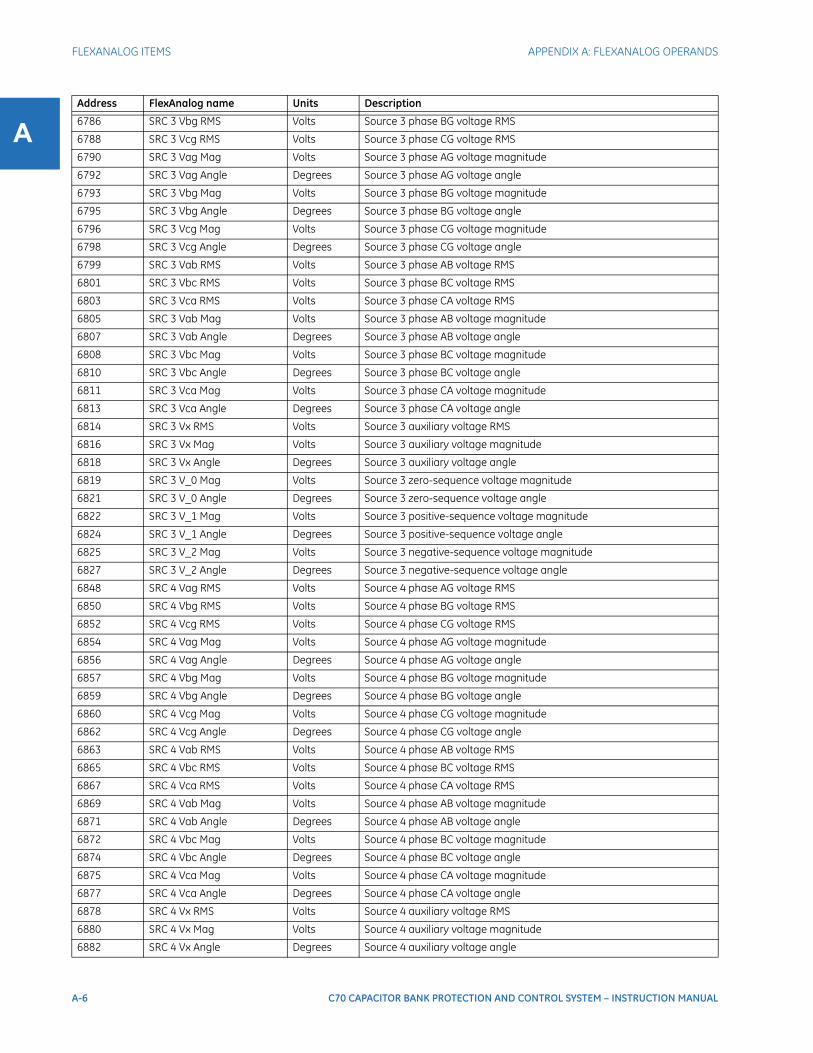
A-6 C70 CAPACITOR BANK PROTECTION AND CONTROL SYSTEM – INSTRUCTION MANUAL
FLEXANALOG ITEMS APPENDIX A: FLEXANALOG OPERANDS
A 6786 SRC 3 Vbg RMS Volts Source 3 phase BG voltage RMS
6788 SRC 3 Vcg RMS Volts Source 3 phase CG voltage RMS
6790 SRC 3 Vag Mag Volts Source 3 phase AG voltage magnitude
6792 SRC 3 Vag Angle Degrees Source 3 phase AG voltage angle
6793 SRC 3 Vbg Mag Volts Source 3 phase BG voltage magnitude
6795 SRC 3 Vbg Angle Degrees Source 3 phase BG voltage angle
6796 SRC 3 Vcg Mag Volts Source 3 phase CG voltage magnitude
6798 SRC 3 Vcg Angle Degrees Source 3 phase CG voltage angle
6799 SRC 3 Vab RMS Volts Source 3 phase AB voltage RMS
6801 SRC 3 Vbc RMS Volts Source 3 phase BC voltage RMS
6803 SRC 3 Vca RMS Volts Source 3 phase CA voltage RMS
6805 SRC 3 Vab Mag Volts Source 3 phase AB voltage magnitude
6807 SRC 3 Vab Angle Degrees Source 3 phase AB voltage angle
6808 SRC 3 Vbc Mag Volts Source 3 phase BC voltage magnitude
6810 SRC 3 Vbc Angle Degrees Source 3 phase BC voltage angle
6811 SRC 3 Vca Mag Volts Source 3 phase CA voltage magnitude
6813 SRC 3 Vca Angle Degrees Source 3 phase CA voltage angle
6814 SRC 3 Vx RMS Volts Source 3 auxiliary voltage RMS
6816 SRC 3 Vx Mag Volts Source 3 auxiliary voltage magnitude
6818 SRC 3 Vx Angle Degrees Source 3 auxiliary voltage angle
6819 SRC 3 V_0 Mag Volts Source 3 zero-sequence voltage magnitude
6821 SRC 3 V_0 Angle Degrees Source 3 zero-sequence voltage angle
6822 SRC 3 V_1 Mag Volts Source 3 positive-sequence voltage magnitude
6824 SRC 3 V_1 Angle Degrees Source 3 positive-sequence voltage angle
6825 SRC 3 V_2 Mag Volts Source 3 negative-sequence voltage magnitude
6827 SRC 3 V_2 Angle Degrees Source 3 negative-sequence voltage angle
6848 SRC 4 Vag RMS Volts Source 4 phase AG voltage RMS
6850 SRC 4 Vbg RMS Volts Source 4 phase BG voltage RMS
6852 SRC 4 Vcg RMS Volts Source 4 phase CG voltage RMS
6854 SRC 4 Vag Mag Volts Source 4 phase AG voltage magnitude
6856 SRC 4 Vag Angle Degrees Source 4 phase AG voltage angle
6857 SRC 4 Vbg Mag Volts Source 4 phase BG voltage magnitude
6859 SRC 4 Vbg Angle Degrees Source 4 phase BG voltage angle
6860 SRC 4 Vcg Mag Volts Source 4 phase CG voltage magnitude
6862 SRC 4 Vcg Angle Degrees Source 4 phase CG voltage angle
6863 SRC 4 Vab RMS Volts Source 4 phase AB voltage RMS
6865 SRC 4 Vbc RMS Volts Source 4 phase BC voltage RMS
6867 SRC 4 Vca RMS Volts Source 4 phase CA voltage RMS
6869 SRC 4 Vab Mag Volts Source 4 phase AB voltage magnitude
6871 SRC 4 Vab Angle Degrees Source 4 phase AB voltage angle
6872 SRC 4 Vbc Mag Volts Source 4 phase BC voltage magnitude
6874 SRC 4 Vbc Angle Degrees Source 4 phase BC voltage angle
6875 SRC 4 Vca Mag Volts Source 4 phase CA voltage magnitude
6877 SRC 4 Vca Angle Degrees Source 4 phase CA voltage angle
6878 SRC 4 Vx RMS Volts Source 4 auxiliary voltage RMS
6880 SRC 4 Vx Mag Volts Source 4 auxiliary voltage magnitude
6882 SRC 4 Vx Angle Degrees Source 4 auxiliary voltage angle
Address FlexAnalog name Units Description

APPENDIX A: FLEXANALOG OPERANDS FLEXANALOG ITEMS
C70 CAPACITOR BANK PROTECTION AND CONTROL SYSTEM – INSTRUCTION MANUAL A-7
A6883 SRC 4 V_0 Mag Volts Source 4 zero-sequence voltage magnitude
6885 SRC 4 V_0 Angle Degrees Source 4 zero-sequence voltage angle
6886 SRC 4 V_1 Mag Volts Source 4 positive-sequence voltage magnitude
6888 SRC 4 V_1 Angle Degrees Source 4 positive-sequence voltage angle
6889 SRC 4 V_2 Mag Volts Source 4 negative-sequence voltage magnitude
6891 SRC 4 V_2 Angle Degrees Source 4 negative-sequence voltage angle
6912 SRC 5 Vag RMS Volts Source 5 phase AG voltage RMS
6914 SRC 5 Vbg RMS Volts Source 5 phase BG voltage RMS
6916 SRC 5 Vcg RMS Volts Source 5 phase CG voltage RMS
6918 SRC 5 Vag Mag Volts Source 5 phase AG voltage magnitude
6920 SRC 5 Vag Angle Degrees Source 5 phase AG voltage angle
6921 SRC 5 Vbg Mag Volts Source 5 phase BG voltage magnitude
6923 SRC 5 Vbg Angle Degrees Source 5 phase BG voltage angle
6924 SRC 5 Vcg Mag Volts Source 5 phase CG voltage magnitude
6926 SRC 5 Vcg Angle Degrees Source 5 phase CG voltage angle
6927 SRC 5 Vab RMS Volts Source 5 phase AB voltage RMS
6929 SRC 5 Vbc RMS Volts Source 5 phase BC voltage RMS
6931 SRC 5 Vca RMS Volts Source 5 phase CA voltage RMS
6933 SRC 5 Vab Mag Volts Source 5 phase AB voltage magnitude
6935 SRC 5 Vab Angle Degrees Source 5 phase AB voltage angle
6936 SRC 5 Vbc Mag Volts Source 5 phase BC voltage magnitude
6938 SRC 5 Vbc Angle Degrees Source 5 phase BC voltage angle
6939 SRC 5 Vca Mag Volts Source 5 phase CA voltage magnitude
6941 SRC 5 Vca Angle Degrees Source 5 phase CA voltage angle
6942 SRC 5 Vx RMS Volts Source 5 auxiliary voltage RMS
6944 SRC 5 Vx Mag Volts Source 5 auxiliary voltage magnitude
6946 SRC 5 Vx Angle Degrees Source 5 auxiliary voltage angle
6947 SRC 5 V_0 Mag Volts Source 5 zero-sequence voltage magnitude
6949 SRC 5 V_0 Angle Degrees Source 5 zero-sequence voltage angle
6950 SRC 5 V_1 Mag Volts Source 5 positive-sequence voltage magnitude
6952 SRC 5 V_1 Angle Degrees Source 5 positive-sequence voltage angle
6953 SRC 5 V_2 Mag Volts Source 5 negative-sequence voltage magnitude
6955 SRC 5 V_2 Angle Degrees Source 5 negative-sequence voltage angle
6976 SRC 6 Vag RMS Volts Source 6 phase AG voltage RMS
6978 SRC 6 Vbg RMS Volts Source 6 phase BG voltage RMS
6980 SRC 6 Vcg RMS Volts Source 6 phase CG voltage RMS
6982 SRC 6 Vag Mag Volts Source 6 phase AG voltage magnitude
6984 SRC 6 Vag Angle Degrees Source 6 phase AG voltage angle
6985 SRC 6 Vbg Mag Volts Source 6 phase BG voltage magnitude
6987 SRC 6 Vbg Angle Degrees Source 6 phase BG voltage angle
6988 SRC 6 Vcg Mag Volts Source 6 phase CG voltage magnitude
6990 SRC 6 Vcg Angle Degrees Source 6 phase CG voltage angle
6991 SRC 6 Vab RMS Volts Source 6 phase AB voltage RMS
6993 SRC 6 Vbc RMS Volts Source 6 phase BC voltage RMS
6995 SRC 6 Vca RMS Volts Source 6 phase CA voltage RMS
6997 SRC 6 Vab Mag Volts Source 6 phase AB voltage magnitude
6999 SRC 6 Vab Angle Degrees Source 6 phase AB voltage angle
Address FlexAnalog name Units Description

A-8 C70 CAPACITOR BANK PROTECTION AND CONTROL SYSTEM – INSTRUCTION MANUAL
FLEXANALOG ITEMS APPENDIX A: FLEXANALOG OPERANDS
A 7000 SRC 6 Vbc Mag Volts Source 6 phase BC voltage magnitude
7002 SRC 6 Vbc Angle Degrees Source 6 phase BC voltage angle
7003 SRC 6 Vca Mag Volts Source 6 phase CA voltage magnitude
7005 SRC 6 Vca Angle Degrees Source 6 phase CA voltage angle
7006 SRC 6 Vx RMS Volts Source 6 auxiliary voltage RMS
7008 SRC 6 Vx Mag Volts Source 6 auxiliary voltage magnitude
7010 SRC 6 Vx Angle Degrees Source 6 auxiliary voltage angle
7011 SRC 6 V_0 Mag Volts Source 6 zero-sequence voltage magnitude
7013 SRC 6 V_0 Angle Degrees Source 6 zero-sequence voltage angle
7014 SRC 6 V_1 Mag Volts Source 6 positive-sequence voltage magnitude
7016 SRC 6 V_1 Angle Degrees Source 6 positive-sequence voltage angle
7017 SRC 6 V_2 Mag Volts Source 6 negative-sequence voltage magnitude
7019 SRC 6 V_2 Angle Degrees Source 6 negative-sequence voltage angle
7168 SRC 1 P Watts Source 1 three-phase real power
7170 SRC 1 Pa Watts Source 1 phase A real power
7172 SRC 1 Pb Watts Source 1 phase B real power
7174 SRC 1 Pc Watts Source 1 phase C real power
7176 SRC 1 Q Vars Source 1 three-phase reactive power
7178 SRC 1 Qa Vars Source 1 phase A reactive power
7180 SRC 1 Qb Vars Source 1 phase B reactive power
7182 SRC 1 Qc Vars Source 1 phase C reactive power
7184 SRC 1 S VA Source 1 three-phase apparent power
7186 SRC 1 Sa VA Source 1 phase A apparent power
7188 SRC 1 Sb VA Source 1 phase B apparent power
7190 SRC 1 Sc VA Source 1 phase C apparent power
7192 SRC 1 PF --- Source 1 three-phase power factor
7193 SRC 1 Phase A PF --- Source 1 phase A power factor
7194 SRC 1 Phase B PF --- Source 1 phase B power factor
7195 SRC 1 Phase C PF --- Source 1 phase C power factor
7200 SRC 2 P Watts Source 2 three-phase real power
7202 SRC 2 Pa Watts Source 2 phase A real power
7204 SRC 2 Pb Watts Source 2 phase B real power
7206 SRC 2 Pc Watts Source 2 phase C real power
7208 SRC 2 Q Vars Source 2 three-phase reactive power
7210 SRC 2 Qa Vars Source 2 phase A reactive power
7212 SRC 2 Qb Vars Source 2 phase B reactive power
7214 SRC 2 Qc Vars Source 2 phase C reactive power
7216 SRC 2 S VA Source 2 three-phase apparent power
7218 SRC 2 Sa VA Source 2 phase A apparent power
7220 SRC 2 Sb VA Source 2 phase B apparent power
7222 SRC 2 Sc VA Source 2 phase C apparent power
7224 SRC 2 PF --- Source 2 three-phase power factor
7225 SRC 2 Phase A PF --- Source 2 phase A power factor
7226 SRC 2 Phase B PF --- Source 2 phase B power factor
7227 SRC 2 Phase C PF --- Source 2 phase C power factor
7232 SRC 3 P Watts Source 3 three-phase real power
7234 SRC 3 Pa Watts Source 3 phase A real power
Address FlexAnalog name Units Description

APPENDIX A: FLEXANALOG OPERANDS FLEXANALOG ITEMS
C70 CAPACITOR BANK PROTECTION AND CONTROL SYSTEM – INSTRUCTION MANUAL A-9
A7236 SRC 3 Pb Watts Source 3 phase B real power
7238 SRC 3 Pc Watts Source 3 phase C real power
7240 SRC 3 Q Vars Source 3 three-phase reactive power
7242 SRC 3 Qa Vars Source 3 phase A reactive power
7244 SRC 3 Qb Vars Source 3 phase B reactive power
7246 SRC 3 Qc Vars Source 3 phase C reactive power
7248 SRC 3 S VA Source 3 three-phase apparent power
7250 SRC 3 Sa VA Source 3 phase A apparent power
7252 SRC 3 Sb VA Source 3 phase B apparent power
7254 SRC 3 Sc VA Source 3 phase C apparent power
7256 SRC 3 PF --- Source 3 three-phase power factor
7257 SRC 3 Phase A PF --- Source 3 phase A power factor
7258 SRC 3 Phase B PF --- Source 3 phase B power factor
7259 SRC 3 Phase C PF --- Source 3 phase C power factor
7264 SRC 4 P Watts Source 4 three-phase real power
7266 SRC 4 Pa Watts Source 4 phase A real power
7268 SRC 4 Pb Watts Source 4 phase B real power
7270 SRC 4 Pc Watts Source 4 phase C real power
7272 SRC 4 Q Vars Source 4 three-phase reactive power
7274 SRC 4 Qa Vars Source 4 phase A reactive power
7276 SRC 4 Qb Vars Source 4 phase B reactive power
7278 SRC 4 Qc Vars Source 4 phase C reactive power
7280 SRC 4 S VA Source 4 three-phase apparent power
7282 SRC 4 Sa VA Source 4 phase A apparent power
7284 SRC 4 Sb VA Source 4 phase B apparent power
7286 SRC 4 Sc VA Source 4 phase C apparent power
7288 SRC 4 PF --- Source 4 three-phase power factor
7289 SRC 4 Phase A PF --- Source 4 phase A power factor
7290 SRC 4 Phase B PF --- Source 4 phase B power factor
7291 SRC 4 Phase C PF --- Source 4 phase C power factor
7296 SRC 5 P Watts Source 5 three-phase real power
7298 SRC 5 Pa Watts Source 5 phase A real power
7300 SRC 5 Pb Watts Source 5 phase B real power
7302 SRC 5 Pc Watts Source 5 phase C real power
7304 SRC 5 Q Vars Source 5 three-phase reactive power
7306 SRC 5 Qa Vars Source 5 phase A reactive power
7308 SRC 5 Qb Vars Source 5 phase B reactive power
7310 SRC 5 Qc Vars Source 5 phase C reactive power
7312 SRC 5 S VA Source 5 three-phase apparent power
7314 SRC 5 Sa VA Source 5 phase A apparent power
7316 SRC 5 Sb VA Source 5 phase B apparent power
7318 SRC 5 Sc VA Source 5 phase C apparent power
7320 SRC 5 PF --- Source 5 three-phase power factor
7321 SRC 5 Phase A PF --- Source 5 phase A power factor
7322 SRC 5 Phase B PF --- Source 5 phase B power factor
7323 SRC 5 Phase C PF --- Source 5 phase C power factor
7328 SRC 6 P Watts Source 6 three-phase real power
Address FlexAnalog name Units Description

A-10 C70 CAPACITOR BANK PROTECTION AND CONTROL SYSTEM – INSTRUCTION MANUAL
FLEXANALOG ITEMS APPENDIX A: FLEXANALOG OPERANDS
A 7330 SRC 6 Pa Watts Source 6 phase A real power
7332 SRC 6 Pb Watts Source 6 phase B real power
7334 SRC 6 Pc Watts Source 6 phase C real power
7336 SRC 6 Q Vars Source 6 three-phase reactive power
7338 SRC 6 Qa Vars Source 6 phase A reactive power
7340 SRC 6 Qb Vars Source 6 phase B reactive power
7342 SRC 6 Qc Vars Source 6 phase C reactive power
7344 SRC 6 S VA Source 6 three-phase apparent power
7346 SRC 6 Sa VA Source 6 phase A apparent power
7348 SRC 6 Sb VA Source 6 phase B apparent power
7350 SRC 6 Sc VA Source 6 phase C apparent power
7352 SRC 6 PF --- Source 6 three-phase power factor
7353 SRC 6 Phase A PF --- Source 6 phase A power factor
7354 SRC 6 Phase B PF --- Source 6 phase B power factor
7355 SRC 6 Phase C PF --- Source 6 phase C power factor
7552 SRC 1 Frequency Hz Source 1 frequency
7554 SRC 2 Frequency Hz Source 2 frequency
7556 SRC 3 Frequency Hz Source 3 frequency
7558 SRC 4 Frequency Hz Source 4 frequency
7560 SRC 5 Frequency Hz Source 5 frequency
7562 SRC 6 Frequency Hz Source 6 frequency
8064 SRC 1 Va THD % Source 1 phase A voltage total harmonic distortion (THD)
8065 SRC 1 Va Harm[0] % Source 1 phase A voltage second harmonic
8066 SRC 1 Va Harm[1] % Source 1 phase A voltage third harmonic
8067 SRC 1 Va Harm[2] % Source 1 phase A voltage fourth harmonic
8068 SRC 1 Va Harm[3] % Source 1 phase A voltage fifth harmonic
8069 SRC 1 Va Harm[4] % Source 1 phase A voltage sixth harmonic
8070 SRC 1 Va Harm[5] % Source 1 phase A voltage seventh harmonic
8071 SRC 1 Va Harm[6] % Source 1 phase A voltage eighth harmonic
8072 SRC 1 Va Harm[7] % Source 1 phase A voltage ninth harmonic
8073 SRC 1 Va Harm[8] % Source 1 phase A voltage tenth harmonic
8074 SRC 1 Va Harm[9] % Source 1 phase A voltage eleventh harmonic
8075 SRC 1 Va Harm[10] % Source 1 phase A voltage twelfth harmonic
8076 SRC 1 Va Harm[11] % Source 1 phase A voltage thirteenth harmonic
8077 SRC 1 Va Harm[12] % Source 1 phase A voltage fourteenth harmonic
8078 SRC 1 Va Harm[13] % Source 1 phase A voltage fifteenth harmonic
8079 SRC 1 Va Harm[14] % Source 1 phase A voltage sixteenth harmonic
8080 SRC 1 Va Harm[15] % Source 1 phase A voltage seventeenth harmonic
8081 SRC 1 Va Harm[16] % Source 1 phase A voltage eighteenth harmonic
8082 SRC 1 Va Harm[17] % Source 1 phase A voltage nineteenth harmonic
8083 SRC 1 Va Harm[18] % Source 1 phase A voltage twentieth harmonic
8084 SRC 1 Va Harm[19] % Source 1 phase A voltage twenty-first harmonic
8085 SRC 1 Va Harm[20] % Source 1 phase A voltage twenty-second harmonic
8086 SRC 1 Va Harm[21] % Source 1 phase A voltage twenty-third harmonic
8087 SRC 1 Va Harm[22] % Source 1 phase A voltage twenty-fourth harmonic
8088 SRC 1 Va Harm[23] % Source 1 phase A voltage twenty-fifth harmonic
8089 SRC 1 Vb THD % Source 1 phase B voltage total harmonic distortion (THD)
Address FlexAnalog name Units Description

APPENDIX A: FLEXANALOG OPERANDS FLEXANALOG ITEMS
C70 CAPACITOR BANK PROTECTION AND CONTROL SYSTEM – INSTRUCTION MANUAL A-11
A8090 SRC 1 Vb Harm[0] % Source 1 phase B voltage second harmonic
8091 SRC 1 Vb Harm[1] % Source 1 phase B voltage third harmonic
8092 SRC 1 Vb Harm[2] % Source 1 phase B voltage fourth harmonic
8093 SRC 1 Vb Harm[3] % Source 1 phase B voltage fifth harmonic
8094 SRC 1 Vb Harm[4] % Source 1 phase B voltage sixth harmonic
8095 SRC 1 Vb Harm[5] % Source 1 phase B voltage seventh harmonic
8096 SRC 1 Vb Harm[6] % Source 1 phase B voltage eighth harmonic
8097 SRC 1 Vb Harm[7] % Source 1 phase B voltage ninth harmonic
8098 SRC 1 Vb Harm[8] % Source 1 phase B voltage tenth harmonic
8099 SRC 1 Vb Harm[9] % Source 1 phase B voltage eleventh harmonic
8100 SRC 1 Vb Harm[10] % Source 1 phase B voltage twelfth harmonic
8101 SRC 1 Vb Harm[11] % Source 1 phase B voltage thirteenth harmonic
8102 SRC 1 Vb Harm[12] % Source 1 phase B voltage fourteenth harmonic
8103 SRC 1 Vb Harm[13] % Source 1 phase B voltage fifteenth harmonic
8104 SRC 1 Vb Harm[14] % Source 1 phase B voltage sixteenth harmonic
8105 SRC 1 Vb Harm[15] % Source 1 phase B voltage seventeenth harmonic
8106 SRC 1 Vb Harm[16] % Source 1 phase B voltage eighteenth harmonic
8107 SRC 1 Vb Harm[17] % Source 1 phase B voltage nineteenth harmonic
8108 SRC 1 Vb Harm[18] % Source 1 phase B voltage twentieth harmonic
8109 SRC 1 Vb Harm[19] % Source 1 phase B voltage twenty-first harmonic
8110 SRC 1 Vb Harm[20] % Source 1 phase B voltage twenty-second harmonic
8111 SRC 1 Vb Harm[21] % Source 1 phase B voltage twenty-third harmonic
8112 SRC 1 Vb Harm[22] % Source 1 phase B voltage twenty-fourth harmonic
8113 SRC 1 Vb Harm[23] % Source 1 phase B voltage twenty-fifth harmonic
8114 SRC 1 Vc THD % Source 1 phase C voltage total harmonic distortion (THD)
8115 SRC 1 Vc Harm[0] % Source 1 phase C voltage second harmonic
8116 SRC 1 Vc Harm[1] % Source 1 phase C voltage third harmonic
8117 SRC 1 Vc Harm[2] % Source 1 phase C voltage fourth harmonic
8118 SRC 1 Vc Harm[3] % Source 1 phase C voltage fifth harmonic
8119 SRC 1 Vc Harm[4] % Source 1 phase C voltage sixth harmonic
8120 SRC 1 Vc Harm[5] % Source 1 phase C voltage seventh harmonic
8121 SRC 1 Vc Harm[6] % Source 1 phase C voltage eighth harmonic
8122 SRC 1 Vc Harm[7] % Source 1 phase C voltage ninth harmonic
8123 SRC 1 Vc Harm[8] % Source 1 phase C voltage tenth harmonic
8124 SRC 1 Vc Harm[9] % Source 1 phase C voltage eleventh harmonic
8125 SRC 1 Vc Harm[10] % Source 1 phase C voltage twelfth harmonic
8126 SRC 1 Vc Harm[11] % Source 1 phase C voltage thirteenth harmonic
8127 SRC 1 Vc Harm[12] % Source 1 phase C voltage fourteenth harmonic
8128 SRC 1 Vc Harm[13] % Source 1 phase C voltage fifteenth harmonic
8129 SRC 1 Vc Harm[14] % Source 1 phase C voltage sixteenth harmonic
8130 SRC 1 Vc Harm[15] % Source 1 phase C voltage seventeenth harmonic
8131 SRC 1 Vc Harm[16] % Source 1 phase C voltage eighteenth harmonic
8132 SRC 1 Vc Harm[17] % Source 1 phase C voltage nineteenth harmonic
8133 SRC 1 Vc Harm[18] % Source 1 phase C voltage twentieth harmonic
8134 SRC 1 Vc Harm[19] % Source 1 phase C voltage twenty-first harmonic
8135 SRC 1 Vc Harm[20] % Source 1 phase C voltage twenty-second harmonic
8136 SRC 1 Vc Harm[21] % Source 1 phase C voltage twenty-third harmonic
Address FlexAnalog name Units Description

A-12 C70 CAPACITOR BANK PROTECTION AND CONTROL SYSTEM – INSTRUCTION MANUAL
FLEXANALOG ITEMS APPENDIX A: FLEXANALOG OPERANDS
A 8137 SRC 1 Vc Harm[22] % Source 1 phase C voltage twenty-fourth harmonic
8138 SRC 1 Vc Harm[23] % Source 1 phase C voltage twenty-fifth harmonic
8139 SRC 2 Va THD % Source 2 phase A voltage total harmonic distortion (THD)
8140 SRC 2 Va Harm[0] % Source 2 phase A voltage second harmonic
8141 SRC 2 Va Harm[1] % Source 2 phase A voltage third harmonic
8142 SRC 2 Va Harm[2] % Source 2 phase A voltage fourth harmonic
8143 SRC 2 Va Harm[3] % Source 2 phase A voltage fifth harmonic
8144 SRC 2 Va Harm[4] % Source 2 phase A voltage sixth harmonic
8145 SRC 2 Va Harm[5] % Source 2 phase A voltage seventh harmonic
8146 SRC 2 Va Harm[6] % Source 2 phase A voltage eighth harmonic
8147 SRC 2 Va Harm[7] % Source 2 phase A voltage ninth harmonic
8148 SRC 2 Va Harm[8] % Source 2 phase A voltage tenth harmonic
8149 SRC 2 Va Harm[9] % Source 2 phase A voltage eleventh harmonic
8150 SRC 2 Va Harm[10] % Source 2 phase A voltage twelfth harmonic
8151 SRC 2 Va Harm[11] % Source 2 phase A voltage thirteenth harmonic
8152 SRC 2 Va Harm[12] % Source 2 phase A voltage fourteenth harmonic
8153 SRC 2 Va Harm[13] % Source 2 phase A voltage fifteenth harmonic
8154 SRC 2 Va Harm[14] % Source 2 phase A voltage sixteenth harmonic
8155 SRC 2 Va Harm[15] % Source 2 phase A voltage seventeenth harmonic
8156 SRC 2 Va Harm[16] % Source 2 phase A voltage eighteenth harmonic
8157 SRC 2 Va Harm[17] % Source 2 phase A voltage nineteenth harmonic
8158 SRC 2 Va Harm[18] % Source 2 phase A voltage twentieth harmonic
8159 SRC 2 Va Harm[19] % Source 2 phase A voltage twenty-first harmonic
8160 SRC 2 Va Harm[20] % Source 2 phase A voltage twenty-second harmonic
8161 SRC 2 Va Harm[21] % Source 2 phase A voltage twenty-third harmonic
8162 SRC 2 Va Harm[22] % Source 2 phase A voltage twenty-fourth harmonic
8163 SRC 2 Va Harm[23] % Source 2 phase A voltage twenty-fifth harmonic
8164 SRC 2 Vb THD % Source 2 phase B voltage total harmonic distortion (THD)
8165 SRC 2 Vb Harm[0] % Source 2 phase B voltage second harmonic
8166 SRC 2 Vb Harm[1] % Source 2 phase B voltage third harmonic
8167 SRC 2 Vb Harm[2] % Source 2 phase B voltage fourth harmonic
8168 SRC 2 Vb Harm[3] % Source 2 phase B voltage fifth harmonic
8169 SRC 2 Vb Harm[4] % Source 2 phase B voltage sixth harmonic
8170 SRC 2 Vb Harm[5] % Source 2 phase B voltage seventh harmonic
8171 SRC 2 Vb Harm[6] % Source 2 phase B voltage eighth harmonic
8172 SRC 2 Vb Harm[7] % Source 2 phase B voltage ninth harmonic
8173 SRC 2 Vb Harm[8] % Source 2 phase B voltage tenth harmonic
8174 SRC 2 Vb Harm[9] % Source 2 phase B voltage eleventh harmonic
8175 SRC 2 Vb Harm[10] % Source 2 phase B voltage twelfth harmonic
8176 SRC 2 Vb Harm[11] % Source 2 phase B voltage thirteenth harmonic
8177 SRC 2 Vb Harm[12] % Source 2 phase B voltage fourteenth harmonic
8178 SRC 2 Vb Harm[13] % Source 2 phase B voltage fifteenth harmonic
8179 SRC 2 Vb Harm[14] % Source 2 phase B voltage sixteenth harmonic
8180 SRC 2 Vb Harm[15] % Source 2 phase B voltage seventeenth harmonic
8181 SRC 2 Vb Harm[16] % Source 2 phase B voltage eighteenth harmonic
8182 SRC 2 Vb Harm[17] % Source 2 phase B voltage nineteenth harmonic
8183 SRC 2 Vb Harm[18] % Source 2 phase B voltage twentieth harmonic
Address FlexAnalog name Units Description
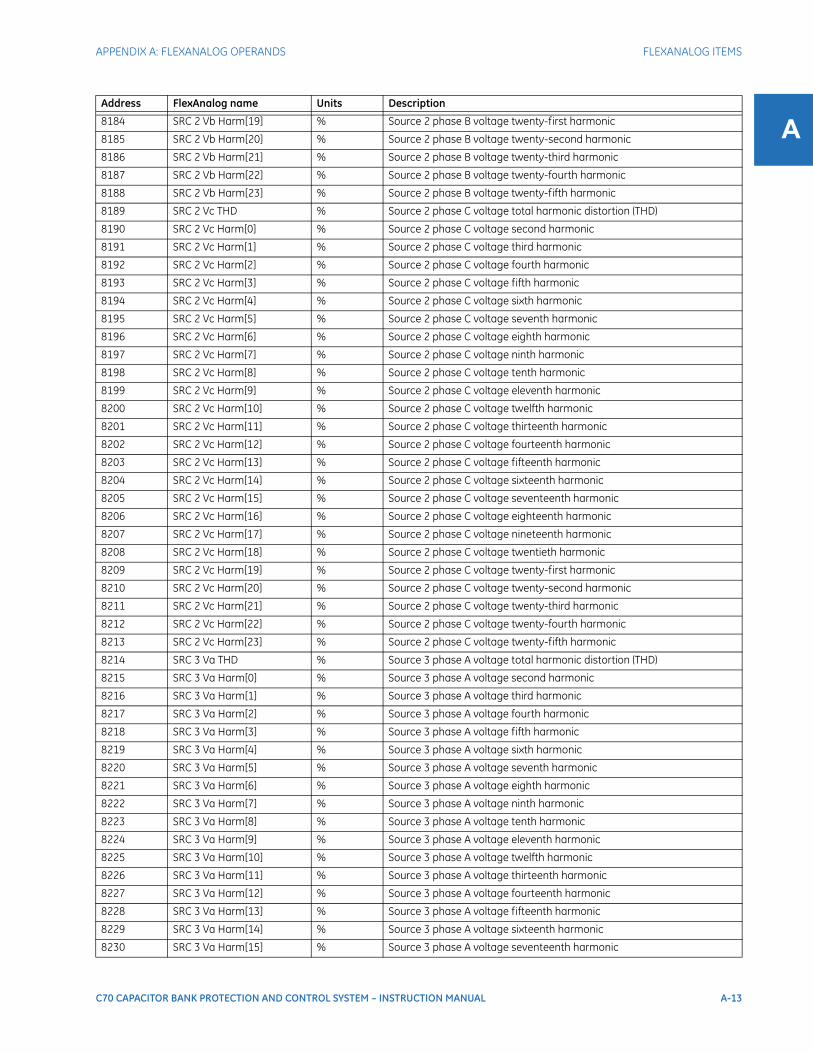
APPENDIX A: FLEXANALOG OPERANDS FLEXANALOG ITEMS
C70 CAPACITOR BANK PROTECTION AND CONTROL SYSTEM – INSTRUCTION MANUAL A-13
A8184 SRC 2 Vb Harm[19] % Source 2 phase B voltage twenty-first harmonic
8185 SRC 2 Vb Harm[20] % Source 2 phase B voltage twenty-second harmonic
8186 SRC 2 Vb Harm[21] % Source 2 phase B voltage twenty-third harmonic
8187 SRC 2 Vb Harm[22] % Source 2 phase B voltage twenty-fourth harmonic
8188 SRC 2 Vb Harm[23] % Source 2 phase B voltage twenty-fifth harmonic
8189 SRC 2 Vc THD % Source 2 phase C voltage total harmonic distortion (THD)
8190 SRC 2 Vc Harm[0] % Source 2 phase C voltage second harmonic
8191 SRC 2 Vc Harm[1] % Source 2 phase C voltage third harmonic
8192 SRC 2 Vc Harm[2] % Source 2 phase C voltage fourth harmonic
8193 SRC 2 Vc Harm[3] % Source 2 phase C voltage fifth harmonic
8194 SRC 2 Vc Harm[4] % Source 2 phase C voltage sixth harmonic
8195 SRC 2 Vc Harm[5] % Source 2 phase C voltage seventh harmonic
8196 SRC 2 Vc Harm[6] % Source 2 phase C voltage eighth harmonic
8197 SRC 2 Vc Harm[7] % Source 2 phase C voltage ninth harmonic
8198 SRC 2 Vc Harm[8] % Source 2 phase C voltage tenth harmonic
8199 SRC 2 Vc Harm[9] % Source 2 phase C voltage eleventh harmonic
8200 SRC 2 Vc Harm[10] % Source 2 phase C voltage twelfth harmonic
8201 SRC 2 Vc Harm[11] % Source 2 phase C voltage thirteenth harmonic
8202 SRC 2 Vc Harm[12] % Source 2 phase C voltage fourteenth harmonic
8203 SRC 2 Vc Harm[13] % Source 2 phase C voltage fifteenth harmonic
8204 SRC 2 Vc Harm[14] % Source 2 phase C voltage sixteenth harmonic
8205 SRC 2 Vc Harm[15] % Source 2 phase C voltage seventeenth harmonic
8206 SRC 2 Vc Harm[16] % Source 2 phase C voltage eighteenth harmonic
8207 SRC 2 Vc Harm[17] % Source 2 phase C voltage nineteenth harmonic
8208 SRC 2 Vc Harm[18] % Source 2 phase C voltage twentieth harmonic
8209 SRC 2 Vc Harm[19] % Source 2 phase C voltage twenty-first harmonic
8210 SRC 2 Vc Harm[20] % Source 2 phase C voltage twenty-second harmonic
8211 SRC 2 Vc Harm[21] % Source 2 phase C voltage twenty-third harmonic
8212 SRC 2 Vc Harm[22] % Source 2 phase C voltage twenty-fourth harmonic
8213 SRC 2 Vc Harm[23] % Source 2 phase C voltage twenty-fifth harmonic
8214 SRC 3 Va THD % Source 3 phase A voltage total harmonic distortion (THD)
8215 SRC 3 Va Harm[0] % Source 3 phase A voltage second harmonic
8216 SRC 3 Va Harm[1] % Source 3 phase A voltage third harmonic
8217 SRC 3 Va Harm[2] % Source 3 phase A voltage fourth harmonic
8218 SRC 3 Va Harm[3] % Source 3 phase A voltage fifth harmonic
8219 SRC 3 Va Harm[4] % Source 3 phase A voltage sixth harmonic
8220 SRC 3 Va Harm[5] % Source 3 phase A voltage seventh harmonic
8221 SRC 3 Va Harm[6] % Source 3 phase A voltage eighth harmonic
8222 SRC 3 Va Harm[7] % Source 3 phase A voltage ninth harmonic
8223 SRC 3 Va Harm[8] % Source 3 phase A voltage tenth harmonic
8224 SRC 3 Va Harm[9] % Source 3 phase A voltage eleventh harmonic
8225 SRC 3 Va Harm[10] % Source 3 phase A voltage twelfth harmonic
8226 SRC 3 Va Harm[11] % Source 3 phase A voltage thirteenth harmonic
8227 SRC 3 Va Harm[12] % Source 3 phase A voltage fourteenth harmonic
8228 SRC 3 Va Harm[13] % Source 3 phase A voltage fifteenth harmonic
8229 SRC 3 Va Harm[14] % Source 3 phase A voltage sixteenth harmonic
8230 SRC 3 Va Harm[15] % Source 3 phase A voltage seventeenth harmonic
Address FlexAnalog name Units Description

A-14 C70 CAPACITOR BANK PROTECTION AND CONTROL SYSTEM – INSTRUCTION MANUAL
FLEXANALOG ITEMS APPENDIX A: FLEXANALOG OPERANDS
A 8231 SRC 3 Va Harm[16] % Source 3 phase A voltage eighteenth harmonic
8232 SRC 3 Va Harm[17] % Source 3 phase A voltage nineteenth harmonic
8233 SRC 3 Va Harm[18] % Source 3 phase A voltage twentieth harmonic
8234 SRC 3 Va Harm[19] % Source 3 phase A voltage twenty-first harmonic
8235 SRC 3 Va Harm[20] % Source 3 phase A voltage twenty-second harmonic
8236 SRC 3 Va Harm[21] % Source 3 phase A voltage twenty-third harmonic
8237 SRC 3 Va Harm[22] % Source 3 phase A voltage twenty-fourth harmonic
8238 SRC 3 Va Harm[23] % Source 3 phase A voltage twenty-fifth harmonic
8239 SRC 3 Vb THD % Source 3 phase B voltage total harmonic distortion (THD)
8240 SRC 3 Vb Harm[0] % Source 3 phase B voltage second harmonic
8241 SRC 3 Vb Harm[1] % Source 3 phase B voltage third harmonic
8242 SRC 3 Vb Harm[2] % Source 3 phase B voltage fourth harmonic
8243 SRC 3 Vb Harm[3] % Source 3 phase B voltage fifth harmonic
8244 SRC 3 Vb Harm[4] % Source 3 phase B voltage sixth harmonic
8245 SRC 3 Vb Harm[5] % Source 3 phase B voltage seventh harmonic
8246 SRC 3 Vb Harm[6] % Source 3 phase B voltage eighth harmonic
8247 SRC 3 Vb Harm[7] % Source 3 phase B voltage ninth harmonic
8248 SRC 3 Vb Harm[8] % Source 3 phase B voltage tenth harmonic
8249 SRC 3 Vb Harm[9] % Source 3 phase B voltage eleventh harmonic
8250 SRC 3 Vb Harm[10] % Source 3 phase B voltage twelfth harmonic
8251 SRC 3 Vb Harm[11] % Source 3 phase B voltage thirteenth harmonic
8252 SRC 3 Vb Harm[12] % Source 3 phase B voltage fourteenth harmonic
8253 SRC 3 Vb Harm[13] % Source 3 phase B voltage fifteenth harmonic
8254 SRC 3 Vb Harm[14] % Source 3 phase B voltage sixteenth harmonic
8255 SRC 3 Vb Harm[15] % Source 3 phase B voltage seventeenth harmonic
8256 SRC 3 Vb Harm[16] % Source 3 phase B voltage eighteenth harmonic
8257 SRC 3 Vb Harm[17] % Source 3 phase B voltage nineteenth harmonic
8258 SRC 3 Vb Harm[18] % Source 3 phase B voltage twentieth harmonic
8259 SRC 3 Vb Harm[19] % Source 3 phase B voltage twenty-first harmonic
8260 SRC 3 Vb Harm[20] % Source 3 phase B voltage twenty-second harmonic
8261 SRC 3 Vb Harm[21] % Source 3 phase B voltage twenty-third harmonic
8262 SRC 3 Vb Harm[22] % Source 3 phase B voltage twenty-fourth harmonic
8263 SRC 3 Vb Harm[23] % Source 3 phase B voltage twenty-fifth harmonic
8264 SRC 3 Vc THD % Source 3 phase C voltage total harmonic distortion (THD)
8265 SRC 3 Vc Harm[0] % Source 3 phase C voltage second harmonic
8266 SRC 3 Vc Harm[1] % Source 3 phase C voltage third harmonic
8267 SRC 3 Vc Harm[2] % Source 3 phase C voltage fourth harmonic
8268 SRC 3 Vc Harm[3] % Source 3 phase C voltage fifth harmonic
8269 SRC 3 Vc Harm[4] % Source 3 phase C voltage sixth harmonic
8270 SRC 3 Vc Harm[5] % Source 3 phase C voltage seventh harmonic
8271 SRC 3 Vc Harm[6] % Source 3 phase C voltage eighth harmonic
8272 SRC 3 Vc Harm[7] % Source 3 phase C voltage ninth harmonic
8273 SRC 3 Vc Harm[8] % Source 3 phase C voltage tenth harmonic
8274 SRC 3 Vc Harm[9] % Source 3 phase C voltage eleventh harmonic
8275 SRC 3 Vc Harm[10] % Source 3 phase C voltage twelfth harmonic
8276 SRC 3 Vc Harm[11] % Source 3 phase C voltage thirteenth harmonic
8277 SRC 3 Vc Harm[12] % Source 3 phase C voltage fourteenth harmonic
Address FlexAnalog name Units Description

APPENDIX A: FLEXANALOG OPERANDS FLEXANALOG ITEMS
C70 CAPACITOR BANK PROTECTION AND CONTROL SYSTEM – INSTRUCTION MANUAL A-15
A8278 SRC 3 Vc Harm[13] % Source 3 phase C voltage fifteenth harmonic
8279 SRC 3 Vc Harm[14] % Source 3 phase C voltage sixteenth harmonic
8280 SRC 3 Vc Harm[15] % Source 3 phase C voltage seventeenth harmonic
8281 SRC 3 Vc Harm[16] % Source 3 phase C voltage eighteenth harmonic
8282 SRC 3 Vc Harm[17] % Source 3 phase C voltage nineteenth harmonic
8283 SRC 3 Vc Harm[18] % Source 3 phase C voltage twentieth harmonic
8284 SRC 3 Vc Harm[19] % Source 3 phase C voltage twenty-first harmonic
8285 SRC 3 Vc Harm[20] % Source 3 phase C voltage twenty-second harmonic
8286 SRC 3 Vc Harm[21] % Source 3 phase C voltage twenty-third harmonic
8287 SRC 3 Vc Harm[22] % Source 3 phase C voltage twenty-fourth harmonic
8288 SRC 3 Vc Harm[23] % Source 3 phase C voltage twenty-fifth harmonic
8289 SRC 4 Va THD % Source 4 phase A voltage total harmonic distortion (THD)
8290 SRC 4 Va Harm[0] % Source 4 phase A voltage second harmonic
8291 SRC 4 Va Harm[1] % Source 4 phase A voltage third harmonic
8292 SRC 4 Va Harm[2] % Source 4 phase A voltage fourth harmonic
8293 SRC 4 Va Harm[3] % Source 4 phase A voltage fifth harmonic
8294 SRC 4 Va Harm[4] % Source 4 phase A voltage sixth harmonic
8295 SRC 4 Va Harm[5] % Source 4 phase A voltage seventh harmonic
8296 SRC 4 Va Harm[6] % Source 4 phase A voltage eighth harmonic
8297 SRC 4 Va Harm[7] % Source 4 phase A voltage ninth harmonic
8298 SRC 4 Va Harm[8] % Source 4 phase A voltage tenth harmonic
8299 SRC 4 Va Harm[9] % Source 4 phase A voltage eleventh harmonic
8300 SRC 4 Va Harm[10] % Source 4 phase A voltage twelfth harmonic
8301 SRC 4 Va Harm[11] % Source 4 phase A voltage thirteenth harmonic
8302 SRC 4 Va Harm[12] % Source 4 phase A voltage fourteenth harmonic
8303 SRC 4 Va Harm[13] % Source 4 phase A voltage fifteenth harmonic
8304 SRC 4 Va Harm[14] % Source 4 phase A voltage sixteenth harmonic
8305 SRC 4 Va Harm[15] % Source 4 phase A voltage seventeenth harmonic
8306 SRC 4 Va Harm[16] % Source 4 phase A voltage eighteenth harmonic
8307 SRC 4 Va Harm[17] % Source 4 phase A voltage nineteenth harmonic
8308 SRC 4 Va Harm[18] % Source 4 phase A voltage twentieth harmonic
8309 SRC 4 Va Harm[19] % Source 4 phase A voltage twenty-first harmonic
8310 SRC 4 Va Harm[20] % Source 4 phase A voltage twenty-second harmonic
8311 SRC 4 Va Harm[21] % Source 4 phase A voltage twenty-third harmonic
8312 SRC 4 Va Harm[22] % Source 4 phase A voltage twenty-fourth harmonic
8313 SRC 4 Va Harm[23] % Source 4 phase A voltage twenty-fifth harmonic
8314 SRC 4 Vb THD % Source 4 phase B voltage total harmonic distortion (THD)
8315 SRC 4 Vb Harm[0] % Source 4 phase B voltage second harmonic
8316 SRC 4 Vb Harm[1] % Source 4 phase B voltage third harmonic
8317 SRC 4 Vb Harm[2] % Source 4 phase B voltage fourth harmonic
8318 SRC 4 Vb Harm[3] % Source 4 phase B voltage fifth harmonic
8319 SRC 4 Vb Harm[4] % Source 4 phase B voltage sixth harmonic
8320 SRC 4 Vb Harm[5] % Source 4 phase B voltage seventh harmonic
8321 SRC 4 Vb Harm[6] % Source 4 phase B voltage eighth harmonic
8322 SRC 4 Vb Harm[7] % Source 4 phase B voltage ninth harmonic
8323 SRC 4 Vb Harm[8] % Source 4 phase B voltage tenth harmonic
8324 SRC 4 Vb Harm[9] % Source 4 phase B voltage eleventh harmonic
Address FlexAnalog name Units Description

A-16 C70 CAPACITOR BANK PROTECTION AND CONTROL SYSTEM – INSTRUCTION MANUAL
FLEXANALOG ITEMS APPENDIX A: FLEXANALOG OPERANDS
A 8325 SRC 4 Vb Harm[10] % Source 4 phase B voltage twelfth harmonic
8326 SRC 4 Vb Harm[11] % Source 4 phase B voltage thirteenth harmonic
8327 SRC 4 Vb Harm[12] % Source 4 phase B voltage fourteenth harmonic
8328 SRC 4 Vb Harm[13] % Source 4 phase B voltage fifteenth harmonic
8329 SRC 4 Vb Harm[14] % Source 4 phase B voltage sixteenth harmonic
8330 SRC 4 Vb Harm[15] % Source 4 phase B voltage seventeenth harmonic
8331 SRC 4 Vb Harm[16] % Source 4 phase B voltage eighteenth harmonic
8332 SRC 4 Vb Harm[17] % Source 4 phase B voltage nineteenth harmonic
8333 SRC 4 Vb Harm[18] % Source 4 phase B voltage twentieth harmonic
8334 SRC 4 Vb Harm[19] % Source 4 phase B voltage twenty-first harmonic
8335 SRC 4 Vb Harm[20] % Source 4 phase B voltage twenty-second harmonic
8336 SRC 4 Vb Harm[21] % Source 4 phase B voltage twenty-third harmonic
8337 SRC 4 Vb Harm[22] % Source 4 phase B voltage twenty-fourth harmonic
8338 SRC 4 Vb Harm[23] % Source 4 phase B voltage twenty-fifth harmonic
8339 SRC 4 Vc THD % Source 4 phase C voltage total harmonic distortion (THD)
8340 SRC 4 Vc Harm[0] % Source 4 phase C voltage second harmonic
8341 SRC 4 Vc Harm[1] % Source 4 phase C voltage third harmonic
8342 SRC 4 Vc Harm[2] % Source 4 phase C voltage fourth harmonic
8343 SRC 4 Vc Harm[3] % Source 4 phase C voltage fifth harmonic
8344 SRC 4 Vc Harm[4] % Source 4 phase C voltage sixth harmonic
8345 SRC 4 Vc Harm[5] % Source 4 phase C voltage seventh harmonic
8346 SRC 4 Vc Harm[6] % Source 4 phase C voltage eighth harmonic
8347 SRC 4 Vc Harm[7] % Source 4 phase C voltage ninth harmonic
8348 SRC 4 Vc Harm[8] % Source 4 phase C voltage tenth harmonic
8349 SRC 4 Vc Harm[9] % Source 4 phase C voltage eleventh harmonic
8350 SRC 4 Vc Harm[10] % Source 4 phase C voltage twelfth harmonic
8351 SRC 4 Vc Harm[11] % Source 4 phase C voltage thirteenth harmonic
8352 SRC 4 Vc Harm[12] % Source 4 phase C voltage fourteenth harmonic
8353 SRC 4 Vc Harm[13] % Source 4 phase C voltage fifteenth harmonic
8354 SRC 4 Vc Harm[14] % Source 4 phase C voltage sixteenth harmonic
8355 SRC 4 Vc Harm[15] % Source 4 phase C voltage seventeenth harmonic
8356 SRC 4 Vc Harm[16] % Source 4 phase C voltage eighteenth harmonic
8357 SRC 4 Vc Harm[17] % Source 4 phase C voltage nineteenth harmonic
8358 SRC 4 Vc Harm[18] % Source 4 phase C voltage twentieth harmonic
8359 SRC 4 Vc Harm[19] % Source 4 phase C voltage twenty-first harmonic
8360 SRC 4 Vc Harm[20] % Source 4 phase C voltage twenty-second harmonic
8361 SRC 4 Vc Harm[21] % Source 4 phase C voltage twenty-third harmonic
8362 SRC 4 Vc Harm[22] % Source 4 phase C voltage twenty-fourth harmonic
8363 SRC 4 Vc Harm[23] % Source 4 phase C voltage twenty-fifth harmonic
8364 SRC 5 Va THD % Source 5 phase A voltage total harmonic distortion (THD)
8365 SRC 5 Va Harm[0] % Source 5 phase A voltage second harmonic
8366 SRC 5 Va Harm[1] % Source 5 phase A voltage third harmonic
8367 SRC 5 Va Harm[2] % Source 5 phase A voltage fourth harmonic
8368 SRC 5 Va Harm[3] % Source 5 phase A voltage fifth harmonic
8369 SRC 5 Va Harm[4] % Source 5 phase A voltage sixth harmonic
8370 SRC 5 Va Harm[5] % Source 5 phase A voltage seventh harmonic
8371 SRC 5 Va Harm[6] % Source 5 phase A voltage eighth harmonic
Address FlexAnalog name Units Description
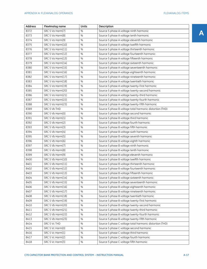
APPENDIX A: FLEXANALOG OPERANDS FLEXANALOG ITEMS
C70 CAPACITOR BANK PROTECTION AND CONTROL SYSTEM – INSTRUCTION MANUAL A-17
A8372 SRC 5 Va Harm[7] % Source 5 phase A voltage ninth harmonic
8373 SRC 5 Va Harm[8] % Source 5 phase A voltage tenth harmonic
8374 SRC 5 Va Harm[9] % Source 5 phase A voltage eleventh harmonic
8375 SRC 5 Va Harm[10] % Source 5 phase A voltage twelfth harmonic
8376 SRC 5 Va Harm[11] % Source 5 phase A voltage thirteenth harmonic
8377 SRC 5 Va Harm[12] % Source 5 phase A voltage fourteenth harmonic
8378 SRC 5 Va Harm[13] % Source 5 phase A voltage fifteenth harmonic
8379 SRC 5 Va Harm[14] % Source 5 phase A voltage sixteenth harmonic
8380 SRC 5 Va Harm[15] % Source 5 phase A voltage seventeenth harmonic
8381 SRC 5 Va Harm[16] % Source 5 phase A voltage eighteenth harmonic
8382 SRC 5 Va Harm[17] % Source 5 phase A voltage nineteenth harmonic
8383 SRC 5 Va Harm[18] % Source 5 phase A voltage twentieth harmonic
8384 SRC 5 Va Harm[19] % Source 5 phase A voltage twenty-first harmonic
8385 SRC 5 Va Harm[20] % Source 5 phase A voltage twenty-second harmonic
8386 SRC 5 Va Harm[21] % Source 5 phase A voltage twenty-third harmonic
8387 SRC 5 Va Harm[22] % Source 5 phase A voltage twenty-fourth harmonic
8388 SRC 5 Va Harm[23] % Source 5 phase A voltage twenty-fifth harmonic
8389 SRC 5 Vb THD % Source 5 phase B voltage total harmonic distortion (THD)
8390 SRC 5 Vb Harm[0] % Source 5 phase B voltage second harmonic
8391 SRC 5 Vb Harm[1] % Source 5 phase B voltage third harmonic
8392 SRC 5 Vb Harm[2] % Source 5 phase B voltage fourth harmonic
8393 SRC 5 Vb Harm[3] % Source 5 phase B voltage fifth harmonic
8394 SRC 5 Vb Harm[4] % Source 5 phase B voltage sixth harmonic
8395 SRC 5 Vb Harm[5] % Source 5 phase B voltage seventh harmonic
8396 SRC 5 Vb Harm[6] % Source 5 phase B voltage eighth harmonic
8397 SRC 5 Vb Harm[7] % Source 5 phase B voltage ninth harmonic
8398 SRC 5 Vb Harm[8] % Source 5 phase B voltage tenth harmonic
8399 SRC 5 Vb Harm[9] % Source 5 phase B voltage eleventh harmonic
8400 SRC 5 Vb Harm[10] % Source 5 phase B voltage twelfth harmonic
8401 SRC 5 Vb Harm[11] % Source 5 phase B voltage thirteenth harmonic
8402 SRC 5 Vb Harm[12] % Source 5 phase B voltage fourteenth harmonic
8403 SRC 5 Vb Harm[13] % Source 5 phase B voltage fifteenth harmonic
8404 SRC 5 Vb Harm[14] % Source 5 phase B voltage sixteenth harmonic
8405 SRC 5 Vb Harm[15] % Source 5 phase B voltage seventeenth harmonic
8406 SRC 5 Vb Harm[16] % Source 5 phase B voltage eighteenth harmonic
8407 SRC 5 Vb Harm[17] % Source 5 phase B voltage nineteenth harmonic
8408 SRC 5 Vb Harm[18] % Source 5 phase B voltage twentieth harmonic
8409 SRC 5 Vb Harm[19] % Source 5 phase B voltage twenty-first harmonic
8410 SRC 5 Vb Harm[20] % Source 5 phase B voltage twenty-second harmonic
8411 SRC 5 Vb Harm[21] % Source 5 phase B voltage twenty-third harmonic
8412 SRC 5 Vb Harm[22] % Source 5 phase B voltage twenty-fourth harmonic
8413 SRC 5 Vb Harm[23] % Source 5 phase B voltage twenty-fifth harmonic
8414 SRC 5 Vc THD % Source 5 phase C voltage total harmonic distortion (THD)
8415 SRC 5 Vc Harm[0] % Source 5 phase C voltage second harmonic
8416 SRC 5 Vc Harm[1] % Source 5 phase C voltage third harmonic
8417 SRC 5 Vc Harm[2] % Source 5 phase C voltage fourth harmonic
8418 SRC 5 Vc Harm[3] % Source 5 phase C voltage fifth harmonic
Address FlexAnalog name Units Description

A-18 C70 CAPACITOR BANK PROTECTION AND CONTROL SYSTEM – INSTRUCTION MANUAL
FLEXANALOG ITEMS APPENDIX A: FLEXANALOG OPERANDS
A 8419 SRC 5 Vc Harm[4] % Source 5 phase C voltage sixth harmonic
8420 SRC 5 Vc Harm[5] % Source 5 phase C voltage seventh harmonic
8421 SRC 5 Vc Harm[6] % Source 5 phase C voltage eighth harmonic
8422 SRC 5 Vc Harm[7] % Source 5 phase C voltage ninth harmonic
8423 SRC 5 Vc Harm[8] % Source 5 phase C voltage tenth harmonic
8424 SRC 5 Vc Harm[9] % Source 5 phase C voltage eleventh harmonic
8425 SRC 5 Vc Harm[10] % Source 5 phase C voltage twelfth harmonic
8426 SRC 5 Vc Harm[11] % Source 5 phase C voltage thirteenth harmonic
8427 SRC 5 Vc Harm[12] % Source 5 phase C voltage fourteenth harmonic
8428 SRC 5 Vc Harm[13] % Source 5 phase C voltage fifteenth harmonic
8429 SRC 5 Vc Harm[14] % Source 5 phase C voltage sixteenth harmonic
8430 SRC 5 Vc Harm[15] % Source 5 phase C voltage seventeenth harmonic
8431 SRC 5 Vc Harm[16] % Source 5 phase C voltage eighteenth harmonic
8432 SRC 5 Vc Harm[17] % Source 5 phase C voltage nineteenth harmonic
8433 SRC 5 Vc Harm[18] % Source 5 phase C voltage twentieth harmonic
8434 SRC 5 Vc Harm[19] % Source 5 phase C voltage twenty-first harmonic
8435 SRC 5 Vc Harm[20] % Source 5 phase C voltage twenty-second harmonic
8436 SRC 5 Vc Harm[21] % Source 5 phase C voltage twenty-third harmonic
8437 SRC 5 Vc Harm[22] % Source 5 phase C voltage twenty-fourth harmonic
8438 SRC 5 Vc Harm[23] % Source 5 phase C voltage twenty-fifth harmonic
8439 SRC 6 Va THD % Source 6 phase A voltage total harmonic distortion (THD)
8440 SRC 6 Va Harm[0] % Source 6 phase A voltage second harmonic
8441 SRC 6 Va Harm[1] % Source 6 phase A voltage third harmonic
8442 SRC 6 Va Harm[2] % Source 6 phase A voltage fourth harmonic
8443 SRC 6 Va Harm[3] % Source 6 phase A voltage fifth harmonic
8444 SRC 6 Va Harm[4] % Source 6 phase A voltage sixth harmonic
8445 SRC 6 Va Harm[5] % Source 6 phase A voltage seventh harmonic
8446 SRC 6 Va Harm[6] % Source 6 phase A voltage eighth harmonic
8447 SRC 6 Va Harm[7] % Source 6 phase A voltage ninth harmonic
8448 SRC 6 Va Harm[8] % Source 6 phase A voltage tenth harmonic
8449 SRC 6 Va Harm[9] % Source 6 phase A voltage eleventh harmonic
8450 SRC 6 Va Harm[10] % Source 6 phase A voltage twelfth harmonic
8451 SRC 6 Va Harm[11] % Source 6 phase A voltage thirteenth harmonic
8452 SRC 6 Va Harm[12] % Source 6 phase A voltage fourteenth harmonic
8453 SRC 6 Va Harm[13] % Source 6 phase A voltage fifteenth harmonic
8454 SRC 6 Va Harm[14] % Source 6 phase A voltage sixteenth harmonic
8455 SRC 6 Va Harm[15] % Source 6 phase A voltage seventeenth harmonic
8456 SRC 6 Va Harm[16] % Source 6 phase A voltage eighteenth harmonic
8457 SRC 6 Va Harm[17] % Source 6 phase A voltage nineteenth harmonic
8458 SRC 6 Va Harm[18] % Source 6 phase A voltage twentieth harmonic
8459 SRC 6 Va Harm[19] % Source 6 phase A voltage twenty-first harmonic
8460 SRC 6 Va Harm[20] % Source 6 phase A voltage twenty-second harmonic
8461 SRC 6 Va Harm[21] % Source 6 phase A voltage twenty-third harmonic
8462 SRC 6 Va Harm[22] % Source 6 phase A voltage twenty-fourth harmonic
8463 SRC 6 Va Harm[23] % Source 6 phase A voltage twenty-fifth harmonic
8464 SRC 6 Vb THD % Source 6 phase B voltage total harmonic distortion (THD)
8465 SRC 6 Vb Harm[0] % Source 6 phase B voltage second harmonic
Address FlexAnalog name Units Description

APPENDIX A: FLEXANALOG OPERANDS FLEXANALOG ITEMS
C70 CAPACITOR BANK PROTECTION AND CONTROL SYSTEM – INSTRUCTION MANUAL A-19
A8466 SRC 6 Vb Harm[1] % Source 6 phase B voltage third harmonic
8467 SRC 6 Vb Harm[2] % Source 6 phase B voltage fourth harmonic
8468 SRC 6 Vb Harm[3] % Source 6 phase B voltage fifth harmonic
8469 SRC 6 Vb Harm[4] % Source 6 phase B voltage sixth harmonic
8470 SRC 6 Vb Harm[5] % Source 6 phase B voltage seventh harmonic
8471 SRC 6 Vb Harm[6] % Source 6 phase B voltage eighth harmonic
8472 SRC 6 Vb Harm[7] % Source 6 phase B voltage ninth harmonic
8473 SRC 6 Vb Harm[8] % Source 6 phase B voltage tenth harmonic
8474 SRC 6 Vb Harm[9] % Source 6 phase B voltage eleventh harmonic
8475 SRC 6 Vb Harm[10] % Source 6 phase B voltage twelfth harmonic
8476 SRC 6 Vb Harm[11] % Source 6 phase B voltage thirteenth harmonic
8477 SRC 6 Vb Harm[12] % Source 6 phase B voltage fourteenth harmonic
8478 SRC 6 Vb Harm[13] % Source 6 phase B voltage fifteenth harmonic
8479 SRC 6 Vb Harm[14] % Source 6 phase B voltage sixteenth harmonic
8480 SRC 6 Vb Harm[15] % Source 6 phase B voltage seventeenth harmonic
8481 SRC 6 Vb Harm[16] % Source 6 phase B voltage eighteenth harmonic
8482 SRC 6 Vb Harm[17] % Source 6 phase B voltage nineteenth harmonic
8483 SRC 6 Vb Harm[18] % Source 6 phase B voltage twentieth harmonic
8484 SRC 6 Vb Harm[19] % Source 6 phase B voltage twenty-first harmonic
8485 SRC 6 Vb Harm[20] % Source 6 phase B voltage twenty-second harmonic
8486 SRC 6 Vb Harm[21] % Source 6 phase B voltage twenty-third harmonic
8487 SRC 6 Vb Harm[22] % Source 6 phase B voltage twenty-fourth harmonic
8488 SRC 6 Vb Harm[23] % Source 6 phase B voltage twenty-fifth harmonic
8489 SRC 6 Vc THD % Source 6 phase C voltage total harmonic distortion (THD)
8490 SRC 6 Vc Harm[0] % Source 6 phase C voltage second harmonic
8491 SRC 6 Vc Harm[1] % Source 6 phase C voltage third harmonic
8492 SRC 6 Vc Harm[2] % Source 6 phase C voltage fourth harmonic
8493 SRC 6 Vc Harm[3] % Source 6 phase C voltage fifth harmonic
8494 SRC 6 Vc Harm[4] % Source 6 phase C voltage sixth harmonic
8495 SRC 6 Vc Harm[5] % Source 6 phase C voltage seventh harmonic
8496 SRC 6 Vc Harm[6] % Source 6 phase C voltage eighth harmonic
8497 SRC 6 Vc Harm[7] % Source 6 phase C voltage ninth harmonic
8498 SRC 6 Vc Harm[8] % Source 6 phase C voltage tenth harmonic
8499 SRC 6 Vc Harm[9] % Source 6 phase C voltage eleventh harmonic
8500 SRC 6 Vc Harm[10] % Source 6 phase C voltage twelfth harmonic
8501 SRC 6 Vc Harm[11] % Source 6 phase C voltage thirteenth harmonic
8502 SRC 6 Vc Harm[12] % Source 6 phase C voltage fourteenth harmonic
8503 SRC 6 Vc Harm[13] % Source 6 phase C voltage fifteenth harmonic
8504 SRC 6 Vc Harm[14] % Source 6 phase C voltage sixteenth harmonic
8505 SRC 6 Vc Harm[15] % Source 6 phase C voltage seventeenth harmonic
8506 SRC 6 Vc Harm[16] % Source 6 phase C voltage eighteenth harmonic
8507 SRC 6 Vc Harm[17] % Source 6 phase C voltage nineteenth harmonic
8508 SRC 6 Vc Harm[18] % Source 6 phase C voltage twentieth harmonic
8509 SRC 6 Vc Harm[19] % Source 6 phase C voltage twenty-first harmonic
8510 SRC 6 Vc Harm[20] % Source 6 phase C voltage twenty-second harmonic
8511 SRC 6 Vc Harm[21] % Source 6 phase C voltage twenty-third harmonic
8512 SRC 6 Vc Harm[22] % Source 6 phase C voltage twenty-fourth harmonic
Address FlexAnalog name Units Description

A-20 C70 CAPACITOR BANK PROTECTION AND CONTROL SYSTEM – INSTRUCTION MANUAL
FLEXANALOG ITEMS APPENDIX A: FLEXANALOG OPERANDS
A 8513 SRC 6 Vc Harm[23] % Source 6 phase C voltage twenty-fifth harmonic
10240 SRC 1 Ia THD % Source 1 phase A current total harmonic distortion
10241 SRC 1 Ia Harm[0] % Source 1 phase A current second harmonic
10242 SRC 1 Ia Harm[1] % Source 1 phase A current third harmonic
10243 SRC 1 Ia Harm[2] % Source 1 phase A current fourth harmonic
10244 SRC 1 Ia Harm[3] % Source 1 phase A current fifth harmonic
10245 SRC 1 Ia Harm[4] % Source 1 phase A current sixth harmonic
10246 SRC 1 Ia Harm[5] % Source 1 phase A current seventh harmonic
10247 SRC 1 Ia Harm[6] % Source 1 phase A current eighth harmonic
10248 SRC 1 Ia Harm[7] % Source 1 phase A current ninth harmonic
10249 SRC 1 Ia Harm[8] % Source 1 phase A current tenth harmonic
10250 SRC 1 Ia Harm[9] % Source 1 phase A current eleventh harmonic
10251 SRC 1 Ia Harm[10] % Source 1 phase A current twelfth harmonic
10252 SRC 1 Ia Harm[11] % Source 1 phase A current thirteenth harmonic
10253 SRC 1 Ia Harm[12] % Source 1 phase A current fourteenth harmonic
10254 SRC 1 Ia Harm[13] % Source 1 phase A current fifteenth harmonic
10255 SRC 1 Ia Harm[14] % Source 1 phase A current sixteenth harmonic
10256 SRC 1 Ia Harm[15] % Source 1 phase A current seventeenth harmonic
10257 SRC 1 Ia Harm[16] % Source 1 phase A current eighteenth harmonic
10258 SRC 1 Ia Harm[17] % Source 1 phase A current nineteenth harmonic
10259 SRC 1 Ia Harm[18] % Source 1 phase A current twentieth harmonic
10260 SRC 1 Ia Harm[19] % Source 1 phase A current twenty-first harmonic
10261 SRC 1 Ia Harm[20] % Source 1 phase A current twenty-second harmonic
10262 SRC 1 Ia Harm[21] % Source 1 phase A current twenty-third harmonic
10263 SRC 1 Ia Harm[22] % Source 1 phase A current twenty-fourth harmonic
10264 SRC 1 Ia Harm[23] % Source 1 phase A current twenty-fifth harmonic
10273 SRC 1 Ib THD % Source 1 phase B current total harmonic distortion
10274 SRC 1 Ib Harm[0] % Source 1 phase B current second harmonic
10275 SRC 1 Ib Harm[1] % Source 1 phase B current third harmonic
10276 SRC 1 Ib Harm[2] % Source 1 phase B current fourth harmonic
10277 SRC 1 Ib Harm[3] % Source 1 phase B current fifth harmonic
10278 SRC 1 Ib Harm[4] % Source 1 phase B current sixth harmonic
10279 SRC 1 Ib Harm[5] % Source 1 phase B current seventh harmonic
10280 SRC 1 Ib Harm[6] % Source 1 phase B current eighth harmonic
10281 SRC 1 Ib Harm[7] % Source 1 phase B current ninth harmonic
10282 SRC 1 Ib Harm[8] % Source 1 phase B current tenth harmonic
10283 SRC 1 Ib Harm[9] % Source 1 phase B current eleventh harmonic
10284 SRC 1 Ib Harm[10] % Source 1 phase B current twelfth harmonic
10285 SRC 1 Ib Harm[11] % Source 1 phase B current thirteenth harmonic
10286 SRC 1 Ib Harm[12] % Source 1 phase B current fourteenth harmonic
10287 SRC 1 Ib Harm[13] % Source 1 phase B current fifteenth harmonic
10288 SRC 1 Ib Harm[14] % Source 1 phase B current sixteenth harmonic
10289 SRC 1 Ib Harm[15] % Source 1 phase B current seventeenth harmonic
10290 SRC 1 Ib Harm[16] % Source 1 phase B current eighteenth harmonic
10291 SRC 1 Ib Harm[17] % Source 1 phase B current nineteenth harmonic
10292 SRC 1 Ib Harm[18] % Source 1 phase B current twentieth harmonic
10293 SRC 1 Ib Harm[19] % Source 1 phase B current twenty-first harmonic
Address FlexAnalog name Units Description

APPENDIX A: FLEXANALOG OPERANDS FLEXANALOG ITEMS
C70 CAPACITOR BANK PROTECTION AND CONTROL SYSTEM – INSTRUCTION MANUAL A-21
A10294 SRC 1 Ib Harm[20] % Source 1 phase B current twenty-second harmonic
10295 SRC 1 Ib Harm[21] % Source 1 phase B current twenty-third harmonic
10296 SRC 1 Ib Harm[22] % Source 1 phase B current twenty-fourth harmonic
10297 SRC 1 Ib Harm[23] % Source 1 phase B current twenty-fifth harmonic
10306 SRC 1 Ic THD % Source 1 phase C current total harmonic distortion
10307 SRC 1 Ic Harm[0] % Source 1 phase C current second harmonic
10308 SRC 1 Ic Harm[1] % Source 1 phase C current third harmonic
10309 SRC 1 Ic Harm[2] % Source 1 phase C current fourth harmonic
10310 SRC 1 Ic Harm[3] % Source 1 phase C current fifth harmonic
10311 SRC 1 Ic Harm[4] % Source 1 phase C current sixth harmonic
10312 SRC 1 Ic Harm[5] % Source 1 phase C current seventh harmonic
10313 SRC 1 Ic Harm[6] % Source 1 phase C current eighth harmonic
10314 SRC 1 Ic Harm[7] % Source 1 phase C current ninth harmonic
10315 SRC 1 Ic Harm[8] % Source 1 phase C current tenth harmonic
10316 SRC 1 Ic Harm[9] % Source 1 phase C current eleventh harmonic
10317 SRC 1 Ic Harm[10] % Source 1 phase C current twelfth harmonic
10318 SRC 1 Ic Harm[11] % Source 1 phase C current thirteenth harmonic
10319 SRC 1 Ic Harm[12] % Source 1 phase C current fourteenth harmonic
10320 SRC 1 Ic Harm[13] % Source 1 phase C current fifteenth harmonic
10321 SRC 1 Ic Harm[14] % Source 1 phase C current sixteenth harmonic
10322 SRC 1 Ic Harm[15] % Source 1 phase C current seventeenth harmonic
10323 SRC 1 Ic Harm[16] % Source 1 phase C current eighteenth harmonic
10324 SRC 1 Ic Harm[17] % Source 1 phase C current nineteenth harmonic
10325 SRC 1 Ic Harm[18] % Source 1 phase C current twentieth harmonic
10326 SRC 1 Ic Harm[19] % Source 1 phase C current twenty-first harmonic
10327 SRC 1 Ic Harm[20] % Source 1 phase C current twenty-second harmonic
10328 SRC 1 Ic Harm[21] % Source 1 phase C current twenty-third harmonic
10329 SRC 1 Ic Harm[22] % Source 1 phase C current twenty-fourth harmonic
10330 SRC 1 Ic Harm[23] % Source 1 phase C current twenty-fifth harmonic
10339 SRC 2 Ia THD % Source 2 phase A current total harmonic distortion
10340 SRC 2 Ia Harm[0] % Source 2 phase A current second harmonic
10341 SRC 2 Ia Harm[1] % Source 2 phase A current third harmonic
10342 SRC 2 Ia Harm[2] % Source 2 phase A current fourth harmonic
10343 SRC 2 Ia Harm[3] % Source 2 phase A current fifth harmonic
10344 SRC 2 Ia Harm[4] % Source 2 phase A current sixth harmonic
10345 SRC 2 Ia Harm[5] % Source 2 phase A current seventh harmonic
10346 SRC 2 Ia Harm[6] % Source 2 phase A current eighth harmonic
10347 SRC 2 Ia Harm[7] % Source 2 phase A current ninth harmonic
10348 SRC 2 Ia Harm[8] % Source 2 phase A current tenth harmonic
10349 SRC 2 Ia Harm[9] % Source 2 phase A current eleventh harmonic
10350 SRC 2 Ia Harm[10] % Source 2 phase A current twelfth harmonic
10351 SRC 2 Ia Harm[11] % Source 2 phase A current thirteenth harmonic
10352 SRC 2 Ia Harm[12] % Source 2 phase A current fourteenth harmonic
10353 SRC 2 Ia Harm[13] % Source 2 phase A current fifteenth harmonic
10354 SRC 2 Ia Harm[14] % Source 2 phase A current sixteenth harmonic
10355 SRC 2 Ia Harm[15] % Source 2 phase A current seventeenth harmonic
10356 SRC 2 Ia Harm[16] % Source 2 phase A current eighteenth harmonic
Address FlexAnalog name Units Description

A-22 C70 CAPACITOR BANK PROTECTION AND CONTROL SYSTEM – INSTRUCTION MANUAL
FLEXANALOG ITEMS APPENDIX A: FLEXANALOG OPERANDS
A 10357 SRC 2 Ia Harm[17] % Source 2 phase A current nineteenth harmonic
10358 SRC 2 Ia Harm[18] % Source 2 phase A current twentieth harmonic
10359 SRC 2 Ia Harm[19] % Source 2 phase A current twenty-first harmonic
10360 SRC 2 Ia Harm[20] % Source 2 phase A current twenty-second harmonic
10361 SRC 2 Ia Harm[21] % Source 2 phase A current twenty-third harmonic
10362 SRC 2 Ia Harm[22] % Source 2 phase A current twenty-fourth harmonic
10363 SRC 2 Ia Harm[23] % Source 2 phase A current twenty-fifth harmonic
10372 SRC 2 Ib THD % Source 2 phase B current total harmonic distortion
10373 SRC 2 Ib Harm[0] % Source 2 phase B current second harmonic
10374 SRC 2 Ib Harm[1] % Source 2 phase B current third harmonic
10375 SRC 2 Ib Harm[2] % Source 2 phase B current fourth harmonic
10376 SRC 2 Ib Harm[3] % Source 2 phase B current fifth harmonic
10377 SRC 2 Ib Harm[4] % Source 2 phase B current sixth harmonic
10378 SRC 2 Ib Harm[5] % Source 2 phase B current seventh harmonic
10379 SRC 2 Ib Harm[6] % Source 2 phase B current eighth harmonic
10380 SRC 2 Ib Harm[7] % Source 2 phase B current ninth harmonic
10381 SRC 2 Ib Harm[8] % Source 2 phase B current tenth harmonic
10382 SRC 2 Ib Harm[9] % Source 2 phase B current eleventh harmonic
10383 SRC 2 Ib Harm[10] % Source 2 phase B current twelfth harmonic
10384 SRC 2 Ib Harm[11] % Source 2 phase B current thirteenth harmonic
10385 SRC 2 Ib Harm[12] % Source 2 phase B current fourteenth harmonic
10386 SRC 2 Ib Harm[13] % Source 2 phase B current fifteenth harmonic
10387 SRC 2 Ib Harm[14] % Source 2 phase B current sixteenth harmonic
10388 SRC 2 Ib Harm[15] % Source 2 phase B current seventeenth harmonic
10389 SRC 2 Ib Harm[16] % Source 2 phase B current eighteenth harmonic
10390 SRC 2 Ib Harm[17] % Source 2 phase B current nineteenth harmonic
10391 SRC 2 Ib Harm[18] % Source 2 phase B current twentieth harmonic
10392 SRC 2 Ib Harm[19] % Source 2 phase B current twenty-first harmonic
10393 SRC 2 Ib Harm[20] % Source 2 phase B current twenty-second harmonic
10394 SRC 2 Ib Harm[21] % Source 2 phase B current twenty-third harmonic
10395 SRC 2 Ib Harm[22] % Source 2 phase B current twenty-fourth harmonic
10396 SRC 2 Ib Harm[23] % Source 2 phase B current twenty-fifth harmonic
10405 SRC 2 Ic THD % Source 2 phase C current total harmonic distortion
10406 SRC 2 Ic Harm[0] % Source 2 phase C current second harmonic
10407 SRC 2 Ic Harm[1] % Source 2 phase C current third harmonic
10408 SRC 2 Ic Harm[2] % Source 2 phase C current fourth harmonic
10409 SRC 2 Ic Harm[3] % Source 2 phase C current fifth harmonic
10410 SRC 2 Ic Harm[4] % Source 2 phase C current sixth harmonic
10411 SRC 2 Ic Harm[5] % Source 2 phase C current seventh harmonic
10412 SRC 2 Ic Harm[6] % Source 2 phase C current eighth harmonic
10413 SRC 2 Ic Harm[7] % Source 2 phase C current ninth harmonic
10414 SRC 2 Ic Harm[8] % Source 2 phase C current tenth harmonic
10415 SRC 2 Ic Harm[9] % Source 2 phase C current eleventh harmonic
10416 SRC 2 Ic Harm[10] % Source 2 phase C current twelfth harmonic
10417 SRC 2 Ic Harm[11] % Source 2 phase C current thirteenth harmonic
10418 SRC 2 Ic Harm[12] % Source 2 phase C current fourteenth harmonic
10419 SRC 2 Ic Harm[13] % Source 2 phase C current fifteenth harmonic
Address FlexAnalog name Units Description
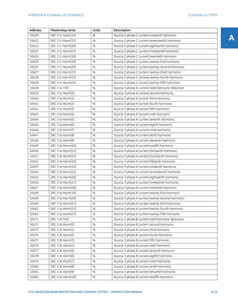
APPENDIX A: FLEXANALOG OPERANDS FLEXANALOG ITEMS
C70 CAPACITOR BANK PROTECTION AND CONTROL SYSTEM – INSTRUCTION MANUAL A-23
A10420 SRC 2 Ic Harm[14] % Source 2 phase C current sixteenth harmonic
10421 SRC 2 Ic Harm[15] % Source 2 phase C current seventeenth harmonic
10422 SRC 2 Ic Harm[16] % Source 2 phase C current eighteenth harmonic
10423 SRC 2 Ic Harm[17] % Source 2 phase C current nineteenth harmonic
10424 SRC 2 Ic Harm[18] % Source 2 phase C current twentieth harmonic
10425 SRC 2 Ic Harm[19] % Source 2 phase C current twenty-first harmonic
10426 SRC 2 Ic Harm[20] % Source 2 phase C current twenty-second harmonic
10427 SRC 2 Ic Harm[21] % Source 2 phase C current twenty-third harmonic
10428 SRC 2 Ic Harm[22] % Source 2 phase C current twenty-fourth harmonic
10429 SRC 2 Ic Harm[23] % Source 2 phase C current twenty-fifth harmonic
10438 SRC 3 Ia THD % Source 3 phase A current total harmonic distortion
10439 SRC 3 Ia Harm[0] % Source 3 phase A current second harmonic
10440 SRC 3 Ia Harm[1] % Source 3 phase A current third harmonic
10441 SRC 3 Ia Harm[2] % Source 3 phase A current fourth harmonic
10442 SRC 3 Ia Harm[3] % Source 3 phase A current fifth harmonic
10443 SRC 3 Ia Harm[4] % Source 3 phase A current sixth harmonic
10444 SRC 3 Ia Harm[5] % Source 3 phase A current seventh harmonic
10445 SRC 3 Ia Harm[6] % Source 3 phase A current eighth harmonic
10446 SRC 3 Ia Harm[7] % Source 3 phase A current ninth harmonic
10447 SRC 3 Ia Harm[8] % Source 3 phase A current tenth harmonic
10448 SRC 3 Ia Harm[9] % Source 3 phase A current eleventh harmonic
10449 SRC 3 Ia Harm[10] % Source 3 phase A current twelfth harmonic
10450 SRC 3 Ia Harm[11] % Source 3 phase A current thirteenth harmonic
10451 SRC 3 Ia Harm[12] % Source 3 phase A current fourteenth harmonic
10452 SRC 3 Ia Harm[13] % Source 3 phase A current fifteenth harmonic
10453 SRC 3 Ia Harm[14] % Source 3 phase A current sixteenth harmonic
10454 SRC 3 Ia Harm[15] % Source 3 phase A current seventeenth harmonic
10455 SRC 3 Ia Harm[16] % Source 3 phase A current eighteenth harmonic
10456 SRC 3 Ia Harm[17] % Source 3 phase A current nineteenth harmonic
10457 SRC 3 Ia Harm[18] % Source 3 phase A current twentieth harmonic
10458 SRC 3 Ia Harm[19] % Source 3 phase A current twenty-first harmonic
10459 SRC 3 Ia Harm[20] % Source 3 phase A current twenty-second harmonic
10460 SRC 3 Ia Harm[21] % Source 3 phase A current twenty-third harmonic
10461 SRC 3 Ia Harm[22] % Source 3 phase A current twenty-fourth harmonic
10462 SRC 3 Ia Harm[23] % Source 3 phase A current twenty-fifth harmonic
10471 SRC 3 Ib THD % Source 3 phase B current total harmonic distortion
10472 SRC 3 Ib Harm[0] % Source 3 phase B current second harmonic
10473 SRC 3 Ib Harm[1] % Source 3 phase B current third harmonic
10474 SRC 3 Ib Harm[2] % Source 3 phase B current fourth harmonic
10475 SRC 3 Ib Harm[3] % Source 3 phase B current fifth harmonic
10476 SRC 3 Ib Harm[4] % Source 3 phase B current sixth harmonic
10477 SRC 3 Ib Harm[5] % Source 3 phase B current seventh harmonic
10478 SRC 3 Ib Harm[6] % Source 3 phase B current eighth harmonic
10479 SRC 3 Ib Harm[7] % Source 3 phase B current ninth harmonic
10480 SRC 3 Ib Harm[8] % Source 3 phase B current tenth harmonic
10481 SRC 3 Ib Harm[9] % Source 3 phase B current eleventh harmonic
10482 SRC 3 Ib Harm[10] % Source 3 phase B current twelfth harmonic
Address FlexAnalog name Units Description
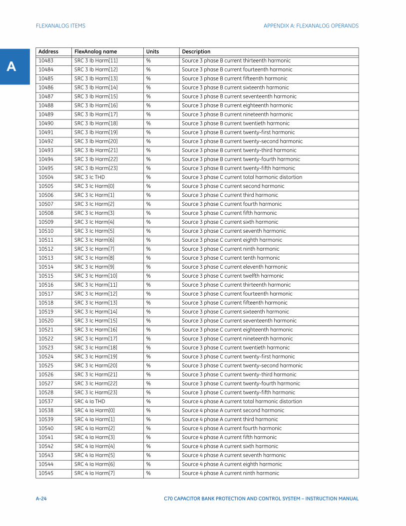
A-24 C70 CAPACITOR BANK PROTECTION AND CONTROL SYSTEM – INSTRUCTION MANUAL
FLEXANALOG ITEMS APPENDIX A: FLEXANALOG OPERANDS
A 10483 SRC 3 Ib Harm[11] % Source 3 phase B current thirteenth harmonic
10484 SRC 3 Ib Harm[12] % Source 3 phase B current fourteenth harmonic
10485 SRC 3 Ib Harm[13] % Source 3 phase B current fifteenth harmonic
10486 SRC 3 Ib Harm[14] % Source 3 phase B current sixteenth harmonic
10487 SRC 3 Ib Harm[15] % Source 3 phase B current seventeenth harmonic
10488 SRC 3 Ib Harm[16] % Source 3 phase B current eighteenth harmonic
10489 SRC 3 Ib Harm[17] % Source 3 phase B current nineteenth harmonic
10490 SRC 3 Ib Harm[18] % Source 3 phase B current twentieth harmonic
10491 SRC 3 Ib Harm[19] % Source 3 phase B current twenty-first harmonic
10492 SRC 3 Ib Harm[20] % Source 3 phase B current twenty-second harmonic
10493 SRC 3 Ib Harm[21] % Source 3 phase B current twenty-third harmonic
10494 SRC 3 Ib Harm[22] % Source 3 phase B current twenty-fourth harmonic
10495 SRC 3 Ib Harm[23] % Source 3 phase B current twenty-fifth harmonic
10504 SRC 3 Ic THD % Source 3 phase C current total harmonic distortion
10505 SRC 3 Ic Harm[0] % Source 3 phase C current second harmonic
10506 SRC 3 Ic Harm[1] % Source 3 phase C current third harmonic
10507 SRC 3 Ic Harm[2] % Source 3 phase C current fourth harmonic
10508 SRC 3 Ic Harm[3] % Source 3 phase C current fifth harmonic
10509 SRC 3 Ic Harm[4] % Source 3 phase C current sixth harmonic
10510 SRC 3 Ic Harm[5] % Source 3 phase C current seventh harmonic
10511 SRC 3 Ic Harm[6] % Source 3 phase C current eighth harmonic
10512 SRC 3 Ic Harm[7] % Source 3 phase C current ninth harmonic
10513 SRC 3 Ic Harm[8] % Source 3 phase C current tenth harmonic
10514 SRC 3 Ic Harm[9] % Source 3 phase C current eleventh harmonic
10515 SRC 3 Ic Harm[10] % Source 3 phase C current twelfth harmonic
10516 SRC 3 Ic Harm[11] % Source 3 phase C current thirteenth harmonic
10517 SRC 3 Ic Harm[12] % Source 3 phase C current fourteenth harmonic
10518 SRC 3 Ic Harm[13] % Source 3 phase C current fifteenth harmonic
10519 SRC 3 Ic Harm[14] % Source 3 phase C current sixteenth harmonic
10520 SRC 3 Ic Harm[15] % Source 3 phase C current seventeenth harmonic
10521 SRC 3 Ic Harm[16] % Source 3 phase C current eighteenth harmonic
10522 SRC 3 Ic Harm[17] % Source 3 phase C current nineteenth harmonic
10523 SRC 3 Ic Harm[18] % Source 3 phase C current twentieth harmonic
10524 SRC 3 Ic Harm[19] % Source 3 phase C current twenty-first harmonic
10525 SRC 3 Ic Harm[20] % Source 3 phase C current twenty-second harmonic
10526 SRC 3 Ic Harm[21] % Source 3 phase C current twenty-third harmonic
10527 SRC 3 Ic Harm[22] % Source 3 phase C current twenty-fourth harmonic
10528 SRC 3 Ic Harm[23] % Source 3 phase C current twenty-fifth harmonic
10537 SRC 4 Ia THD % Source 4 phase A current total harmonic distortion
10538 SRC 4 Ia Harm[0] % Source 4 phase A current second harmonic
10539 SRC 4 Ia Harm[1] % Source 4 phase A current third harmonic
10540 SRC 4 Ia Harm[2] % Source 4 phase A current fourth harmonic
10541 SRC 4 Ia Harm[3] % Source 4 phase A current fifth harmonic
10542 SRC 4 Ia Harm[4] % Source 4 phase A current sixth harmonic
10543 SRC 4 Ia Harm[5] % Source 4 phase A current seventh harmonic
10544 SRC 4 Ia Harm[6] % Source 4 phase A current eighth harmonic
10545 SRC 4 Ia Harm[7] % Source 4 phase A current ninth harmonic
Address FlexAnalog name Units Description

APPENDIX A: FLEXANALOG OPERANDS FLEXANALOG ITEMS
C70 CAPACITOR BANK PROTECTION AND CONTROL SYSTEM – INSTRUCTION MANUAL A-25
A10546 SRC 4 Ia Harm[8] % Source 4 phase A current tenth harmonic
10547 SRC 4 Ia Harm[9] % Source 4 phase A current eleventh harmonic
10548 SRC 4 Ia Harm[10] % Source 4 phase A current twelfth harmonic
10549 SRC 4 Ia Harm[11] % Source 4 phase A current thirteenth harmonic
10550 SRC 4 Ia Harm[12] % Source 4 phase A current fourteenth harmonic
10551 SRC 4 Ia Harm[13] % Source 4 phase A current fifteenth harmonic
10552 SRC 4 Ia Harm[14] % Source 4 phase A current sixteenth harmonic
10553 SRC 4 Ia Harm[15] % Source 4 phase A current seventeenth harmonic
10554 SRC 4 Ia Harm[16] % Source 4 phase A current eighteenth harmonic
10555 SRC 4 Ia Harm[17] % Source 4 phase A current nineteenth harmonic
10556 SRC 4 Ia Harm[18] % Source 4 phase A current twentieth harmonic
10557 SRC 4 Ia Harm[19] % Source 4 phase A current twenty-first harmonic
10558 SRC 4 Ia Harm[20] % Source 4 phase A current twenty-second harmonic
10559 SRC 4 Ia Harm[21] % Source 4 phase A current twenty-third harmonic
10560 SRC 4 Ia Harm[22] % Source 4 phase A current twenty-fourth harmonic
10561 SRC 4 Ia Harm[23] % Source 4 phase A current twenty-fifth harmonic
10570 SRC 4 Ib THD % Source 4 phase B current total harmonic distortion
10571 SRC 4 Ib Harm[0] % Source 4 phase B current second harmonic
10572 SRC 4 Ib Harm[1] % Source 4 phase B current third harmonic
10573 SRC 4 Ib Harm[2] % Source 4 phase B current fourth harmonic
10574 SRC 4 Ib Harm[3] % Source 4 phase B current fifth harmonic
10575 SRC 4 Ib Harm[4] % Source 4 phase B current sixth harmonic
10576 SRC 4 Ib Harm[5] % Source 4 phase B current seventh harmonic
10577 SRC 4 Ib Harm[6] % Source 4 phase B current eighth harmonic
10578 SRC 4 Ib Harm[7] % Source 4 phase B current ninth harmonic
10579 SRC 4 Ib Harm[8] % Source 4 phase B current tenth harmonic
10580 SRC 4 Ib Harm[9] % Source 4 phase B current eleventh harmonic
10581 SRC 4 Ib Harm[10] % Source 4 phase B current twelfth harmonic
10582 SRC 4 Ib Harm[11] % Source 4 phase B current thirteenth harmonic
10583 SRC 4 Ib Harm[12] % Source 4 phase B current fourteenth harmonic
10584 SRC 4 Ib Harm[13] % Source 4 phase B current fifteenth harmonic
10585 SRC 4 Ib Harm[14] % Source 4 phase B current sixteenth harmonic
10586 SRC 4 Ib Harm[15] % Source 4 phase B current seventeenth harmonic
10587 SRC 4 Ib Harm[16] % Source 4 phase B current eighteenth harmonic
10588 SRC 4 Ib Harm[17] % Source 4 phase B current nineteenth harmonic
10589 SRC 4 Ib Harm[18] % Source 4 phase B current twentieth harmonic
10590 SRC 4 Ib Harm[19] % Source 4 phase B current twenty-first harmonic
10591 SRC 4 Ib Harm[20] % Source 4 phase B current twenty-second harmonic
10592 SRC 4 Ib Harm[21] % Source 4 phase B current twenty-third harmonic
10593 SRC 4 Ib Harm[22] % Source 4 phase B current twenty-fourth harmonic
10594 SRC 4 Ib Harm[23] % Source 4 phase B current twenty-fifth harmonic
10603 SRC 4 Ic THD % Source 4 phase C current total harmonic distortion
10604 SRC 4 Ic Harm[0] % Source 4 phase C current second harmonic
10605 SRC 4 Ic Harm[1] % Source 4 phase C current third harmonic
10606 SRC 4 Ic Harm[2] % Source 4 phase C current fourth harmonic
10607 SRC 4 Ic Harm[3] % Source 4 phase C current fifth harmonic
10608 SRC 4 Ic Harm[4] % Source 4 phase C current sixth harmonic
Address FlexAnalog name Units Description

A-26 C70 CAPACITOR BANK PROTECTION AND CONTROL SYSTEM – INSTRUCTION MANUAL
FLEXANALOG ITEMS APPENDIX A: FLEXANALOG OPERANDS
A 10609 SRC 4 Ic Harm[5] % Source 4 phase C current seventh harmonic
10610 SRC 4 Ic Harm[6] % Source 4 phase C current eighth harmonic
10611 SRC 4 Ic Harm[7] % Source 4 phase C current ninth harmonic
10612 SRC 4 Ic Harm[8] % Source 4 phase C current tenth harmonic
10613 SRC 4 Ic Harm[9] % Source 4 phase C current eleventh harmonic
10614 SRC 4 Ic Harm[10] % Source 4 phase C current twelfth harmonic
10615 SRC 4 Ic Harm[11] % Source 4 phase C current thirteenth harmonic
10616 SRC 4 Ic Harm[12] % Source 4 phase C current fourteenth harmonic
10617 SRC 4 Ic Harm[13] % Source 4 phase C current fifteenth harmonic
10618 SRC 4 Ic Harm[14] % Source 4 phase C current sixteenth harmonic
10619 SRC 4 Ic Harm[15] % Source 4 phase C current seventeenth harmonic
10620 SRC 4 Ic Harm[16] % Source 4 phase C current eighteenth harmonic
10621 SRC 4 Ic Harm[17] % Source 4 phase C current nineteenth harmonic
10622 SRC 4 Ic Harm[18] % Source 4 phase C current twentieth harmonic
10623 SRC 4 Ic Harm[19] % Source 4 phase C current twenty-first harmonic
10624 SRC 4 Ic Harm[20] % Source 4 phase C current twenty-second harmonic
10625 SRC 4 Ic Harm[21] % Source 4 phase C current twenty-third harmonic
10626 SRC 4 Ic Harm[22] % Source 4 phase C current twenty-fourth harmonic
10627 SRC 4 Ic Harm[23] % Source 4 phase C current twenty-fifth harmonic
10636 SRC 5 Ia THD % Source 5 phase A current total harmonic distortion
10637 SRC 5 Ia Harm[0] % Source 5 phase A current second harmonic
10638 SRC 5 Ia Harm[1] % Source 5 phase A current third harmonic
10639 SRC 5 Ia Harm[2] % Source 5 phase A current fourth harmonic
10640 SRC 5 Ia Harm[3] % Source 5 phase A current fifth harmonic
10641 SRC 5 Ia Harm[4] % Source 5 phase A current sixth harmonic
10642 SRC 5 Ia Harm[5] % Source 5 phase A current seventh harmonic
10643 SRC 5 Ia Harm[6] % Source 5 phase A current eighth harmonic
10644 SRC 5 Ia Harm[7] % Source 5 phase A current ninth harmonic
10645 SRC 5 Ia Harm[8] % Source 5 phase A current tenth harmonic
10646 SRC 5 Ia Harm[9] % Source 5 phase A current eleventh harmonic
10647 SRC 5 Ia Harm[10] % Source 5 phase A current twelfth harmonic
10648 SRC 5 Ia Harm[11] % Source 5 phase A current thirteenth harmonic
10649 SRC 5 Ia Harm[12] % Source 5 phase A current fourteenth harmonic
10650 SRC 5 Ia Harm[13] % Source 5 phase A current fifteenth harmonic
10651 SRC 5 Ia Harm[14] % Source 5 phase A current sixteenth harmonic
10652 SRC 5 Ia Harm[15] % Source 5 phase A current seventeenth harmonic
10653 SRC 5 Ia Harm[16] % Source 5 phase A current eighteenth harmonic
10654 SRC 5 Ia Harm[17] % Source 5 phase A current nineteenth harmonic
10655 SRC 5 Ia Harm[18] % Source 5 phase A current twentieth harmonic
10656 SRC 5 Ia Harm[19] % Source 5 phase A current twenty-first harmonic
10657 SRC 5 Ia Harm[20] % Source 5 phase A current twenty-second harmonic
10658 SRC 5 Ia Harm[21] % Source 5 phase A current twenty-third harmonic
10659 SRC 5 Ia Harm[22] % Source 5 phase A current twenty-fourth harmonic
10660 SRC 5 Ia Harm[23] % Source 5 phase A current twenty-fifth harmonic
10669 SRC 5 Ib THD % Source 5 phase B current total harmonic distortion
10670 SRC 5 Ib Harm[0] % Source 5 phase B current second harmonic
10671 SRC 5 Ib Harm[1] % Source 5 phase B current third harmonic
Address FlexAnalog name Units Description

APPENDIX A: FLEXANALOG OPERANDS FLEXANALOG ITEMS
C70 CAPACITOR BANK PROTECTION AND CONTROL SYSTEM – INSTRUCTION MANUAL A-27
A10672 SRC 5 Ib Harm[2] % Source 5 phase B current fourth harmonic
10673 SRC 5 Ib Harm[3] % Source 5 phase B current fifth harmonic
10674 SRC 5 Ib Harm[4] % Source 5 phase B current sixth harmonic
10675 SRC 5 Ib Harm[5] % Source 5 phase B current seventh harmonic
10676 SRC 5 Ib Harm[6] % Source 5 phase B current eighth harmonic
10677 SRC 5 Ib Harm[7] % Source 5 phase B current ninth harmonic
10678 SRC 5 Ib Harm[8] % Source 5 phase B current tenth harmonic
10679 SRC 5 Ib Harm[9] % Source 5 phase B current eleventh harmonic
10680 SRC 5 Ib Harm[10] % Source 5 phase B current twelfth harmonic
10681 SRC 5 Ib Harm[11] % Source 5 phase B current thirteenth harmonic
10682 SRC 5 Ib Harm[12] % Source 5 phase B current fourteenth harmonic
10683 SRC 5 Ib Harm[13] % Source 5 phase B current fifteenth harmonic
10684 SRC 5 Ib Harm[14] % Source 5 phase B current sixteenth harmonic
10685 SRC 5 Ib Harm[15] % Source 5 phase B current seventeenth harmonic
10686 SRC 5 Ib Harm[16] % Source 5 phase B current eighteenth harmonic
10687 SRC 5 Ib Harm[17] % Source 5 phase B current nineteenth harmonic
10688 SRC 5 Ib Harm[18] % Source 5 phase B current twentieth harmonic
10689 SRC 5 Ib Harm[19] % Source 5 phase B current twenty-first harmonic
10690 SRC 5 Ib Harm[20] % Source 5 phase B current twenty-second harmonic
10691 SRC 5 Ib Harm[21] % Source 5 phase B current twenty-third harmonic
10692 SRC 5 Ib Harm[22] % Source 5 phase B current twenty-fourth harmonic
10693 SRC 5 Ib Harm[23] % Source 5 phase B current twenty-fifth harmonic
10702 SRC 5 Ic THD % Source 5 phase C current total harmonic distortion
10703 SRC 5 Ic Harm[0] % Source 5 phase C current second harmonic
10704 SRC 5 Ic Harm[1] % Source 5 phase C current third harmonic
10705 SRC 5 Ic Harm[2] % Source 5 phase C current fourth harmonic
10706 SRC 5 Ic Harm[3] % Source 5 phase C current fifth harmonic
10707 SRC 5 Ic Harm[4] % Source 5 phase C current sixth harmonic
10708 SRC 5 Ic Harm[5] % Source 5 phase C current seventh harmonic
10709 SRC 5 Ic Harm[6] % Source 5 phase C current eighth harmonic
10710 SRC 5 Ic Harm[7] % Source 5 phase C current ninth harmonic
10711 SRC 5 Ic Harm[8] % Source 5 phase C current tenth harmonic
10712 SRC 5 Ic Harm[9] % Source 5 phase C current eleventh harmonic
10713 SRC 5 Ic Harm[10] % Source 5 phase C current twelfth harmonic
10714 SRC 5 Ic Harm[11] % Source 5 phase C current thirteenth harmonic
10715 SRC 5 Ic Harm[12] % Source 5 phase C current fourteenth harmonic
10716 SRC 5 Ic Harm[13] % Source 5 phase C current fifteenth harmonic
10717 SRC 5 Ic Harm[14] % Source 5 phase C current sixteenth harmonic
10718 SRC 5 Ic Harm[15] % Source 5 phase C current seventeenth harmonic
10719 SRC 5 Ic Harm[16] % Source 5 phase C current eighteenth harmonic
10720 SRC 5 Ic Harm[17] % Source 5 phase C current nineteenth harmonic
10721 SRC 5 Ic Harm[18] % Source 5 phase C current twentieth harmonic
10722 SRC 5 Ic Harm[19] % Source 5 phase C current twenty-first harmonic
10723 SRC 5 Ic Harm[20] % Source 5 phase C current twenty-second harmonic
10724 SRC 5 Ic Harm[21] % Source 5 phase C current twenty-third harmonic
10725 SRC 5 Ic Harm[22] % Source 5 phase C current twenty-fourth harmonic
10726 SRC 5 Ic Harm[23] % Source 5 phase C current twenty-fifth harmonic
Address FlexAnalog name Units Description

A-28 C70 CAPACITOR BANK PROTECTION AND CONTROL SYSTEM – INSTRUCTION MANUAL
FLEXANALOG ITEMS APPENDIX A: FLEXANALOG OPERANDS
A 10735 SRC 6 Ia THD % Source 6 phase A current total harmonic distortion
10736 SRC 6 Ia Harm[0] % Source 6 phase A current second harmonic
10737 SRC 6 Ia Harm[1] % Source 6 phase A current third harmonic
10738 SRC 6 Ia Harm[2] % Source 6 phase A current fourth harmonic
10739 SRC 6 Ia Harm[3] % Source 6 phase A current fifth harmonic
10740 SRC 6 Ia Harm[4] % Source 6 phase A current sixth harmonic
10741 SRC 6 Ia Harm[5] % Source 6 phase A current seventh harmonic
10742 SRC 6 Ia Harm[6] % Source 6 phase A current eighth harmonic
10743 SRC 6 Ia Harm[7] % Source 6 phase A current ninth harmonic
10744 SRC 6 Ia Harm[8] % Source 6 phase A current tenth harmonic
10745 SRC 6 Ia Harm[9] % Source 6 phase A current eleventh harmonic
10746 SRC 6 Ia Harm[10] % Source 6 phase A current twelfth harmonic
10747 SRC 6 Ia Harm[11] % Source 6 phase A current thirteenth harmonic
10748 SRC 6 Ia Harm[12] % Source 6 phase A current fourteenth harmonic
10749 SRC 6 Ia Harm[13] % Source 6 phase A current fifteenth harmonic
10750 SRC 6 Ia Harm[14] % Source 6 phase A current sixteenth harmonic
10751 SRC 6 Ia Harm[15] % Source 6 phase A current seventeenth harmonic
10752 SRC 6 Ia Harm[16] % Source 6 phase A current eighteenth harmonic
10753 SRC 6 Ia Harm[17] % Source 6 phase A current nineteenth harmonic
10754 SRC 6 Ia Harm[18] % Source 6 phase A current twentieth harmonic
10755 SRC 6 Ia Harm[19] % Source 6 phase A current twenty-first harmonic
10756 SRC 6 Ia Harm[20] % Source 6 phase A current twenty-second harmonic
10757 SRC 6 Ia Harm[21] % Source 6 phase A current twenty-third harmonic
10758 SRC 6 Ia Harm[22] % Source 6 phase A current twenty-fourth harmonic
10759 SRC 6 Ia Harm[23] % Source 6 phase A current twenty-fifth harmonic
10768 SRC 6 Ib THD % Source 6 phase B current total harmonic distortion
10769 SRC 6 Ib Harm[0] % Source 6 phase B current second harmonic
10770 SRC 6 Ib Harm[1] % Source 6 phase B current third harmonic
10771 SRC 6 Ib Harm[2] % Source 6 phase B current fourth harmonic
10772 SRC 6 Ib Harm[3] % Source 6 phase B current fifth harmonic
10773 SRC 6 Ib Harm[4] % Source 6 phase B current sixth harmonic
10774 SRC 6 Ib Harm[5] % Source 6 phase B current seventh harmonic
10775 SRC 6 Ib Harm[6] % Source 6 phase B current eighth harmonic
10776 SRC 6 Ib Harm[7] % Source 6 phase B current ninth harmonic
10777 SRC 6 Ib Harm[8] % Source 6 phase B current tenth harmonic
10778 SRC 6 Ib Harm[9] % Source 6 phase B current eleventh harmonic
10779 SRC 6 Ib Harm[10] % Source 6 phase B current twelfth harmonic
10780 SRC 6 Ib Harm[11] % Source 6 phase B current thirteenth harmonic
10781 SRC 6 Ib Harm[12] % Source 6 phase B current fourteenth harmonic
10782 SRC 6 Ib Harm[13] % Source 6 phase B current fifteenth harmonic
10783 SRC 6 Ib Harm[14] % Source 6 phase B current sixteenth harmonic
10784 SRC 6 Ib Harm[15] % Source 6 phase B current seventeenth harmonic
10785 SRC 6 Ib Harm[16] % Source 6 phase B current eighteenth harmonic
10786 SRC 6 Ib Harm[17] % Source 6 phase B current nineteenth harmonic
10787 SRC 6 Ib Harm[18] % Source 6 phase B current twentieth harmonic
10788 SRC 6 Ib Harm[19] % Source 6 phase B current twenty-first harmonic
10789 SRC 6 Ib Harm[20] % Source 6 phase B current twenty-second harmonic
Address FlexAnalog name Units Description

APPENDIX A: FLEXANALOG OPERANDS FLEXANALOG ITEMS
C70 CAPACITOR BANK PROTECTION AND CONTROL SYSTEM – INSTRUCTION MANUAL A-29
A10790 SRC 6 Ib Harm[21] % Source 6 phase B current twenty-third harmonic
10791 SRC 6 Ib Harm[22] % Source 6 phase B current twenty-fourth harmonic
10792 SRC 6 Ib Harm[23] % Source 6 phase B current twenty-fifth harmonic
10801 SRC 6 Ic THD % Source 6 phase C current total harmonic distortion
10802 SRC 6 Ic Harm[0] % Source 6 phase C current second harmonic
10803 SRC 6 Ic Harm[1] % Source 6 phase C current third harmonic
10804 SRC 6 Ic Harm[2] % Source 6 phase C current fourth harmonic
10805 SRC 6 Ic Harm[3] % Source 6 phase C current fifth harmonic
10806 SRC 6 Ic Harm[4] % Source 6 phase C current sixth harmonic
10807 SRC 6 Ic Harm[5] % Source 6 phase C current seventh harmonic
10808 SRC 6 Ic Harm[6] % Source 6 phase C current eighth harmonic
10809 SRC 6 Ic Harm[7] % Source 6 phase C current ninth harmonic
10810 SRC 6 Ic Harm[8] % Source 6 phase C current tenth harmonic
10811 SRC 6 Ic Harm[9] % Source 6 phase C current eleventh harmonic
10812 SRC 6 Ic Harm[10] % Source 6 phase C current twelfth harmonic
10813 SRC 6 Ic Harm[11] % Source 6 phase C current thirteenth harmonic
10814 SRC 6 Ic Harm[12] % Source 6 phase C current fourteenth harmonic
10815 SRC 6 Ic Harm[13] % Source 6 phase C current fifteenth harmonic
10816 SRC 6 Ic Harm[14] % Source 6 phase C current sixteenth harmonic
10817 SRC 6 Ic Harm[15] % Source 6 phase C current seventeenth harmonic
10818 SRC 6 Ic Harm[16] % Source 6 phase C current eighteenth harmonic
10819 SRC 6 Ic Harm[17] % Source 6 phase C current nineteenth harmonic
10820 SRC 6 Ic Harm[18] % Source 6 phase C current twentieth harmonic
10821 SRC 6 Ic Harm[19] % Source 6 phase C current twenty-first harmonic
10822 SRC 6 Ic Harm[20] % Source 6 phase C current twenty-second harmonic
10823 SRC 6 Ic Harm[21] % Source 6 phase C current twenty-third harmonic
10824 SRC 6 Ic Harm[22] % Source 6 phase C current twenty-fourth harmonic
10825 SRC 6 Ic Harm[23] % Source 6 phase C current twenty-fifth harmonic
12306 Oscill Num Triggers --- Oscillography number of triggers
13504 DCmA Inputs 1 Value mA DCmA input 1 actual value
13506 DCmA Inputs 2 Value mA DCmA input 2 actual value
13508 DCmA Inputs 3 Value mA DCmA input 3 actual value
13510 DCmA Inputs 4 Value mA DCmA input 4 actual value
13512 DCmA Inputs 5 Value mA DCmA input 5 actual value
13514 DCmA Inputs 6 Value mA DCmA input 6 actual value
13516 DCmA Inputs 7 Value mA DCmA input 7 actual value
13518 DCmA Inputs 8 Value mA DCmA input 8 actual value
13520 DCmA Inputs 9 Value mA DCmA input 9 actual value
13522 DCmA Inputs 10 Value mA DCmA input 10 actual value
13524 DCmA Inputs 11 Value mA DCmA input 11 actual value
13526 DCmA Inputs 12 Value mA DCmA input 12 actual value
13528 DCmA Inputs 13 Value mA DCmA input 13 actual value
13530 DCmA Inputs 14 Value mA DCmA input 14 actual value
13532 DCmA Inputs 15 Value mA DCmA input 15 actual value
13534 DCmA Inputs 16 Value mA DCmA input 16 actual value
13536 DCmA Inputs 17 Value mA DCmA input 17 actual value
13538 DCmA Inputs 18 Value mA DCmA input 18 actual value
Address FlexAnalog name Units Description
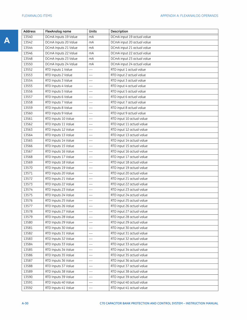
A-30 C70 CAPACITOR BANK PROTECTION AND CONTROL SYSTEM – INSTRUCTION MANUAL
FLEXANALOG ITEMS APPENDIX A: FLEXANALOG OPERANDS
A 13540 DCmA Inputs 19 Value mA DCmA input 19 actual value
13542 DCmA Inputs 20 Value mA DCmA input 20 actual value
13544 DCmA Inputs 21 Value mA DCmA input 21 actual value
13546 DCmA Inputs 22 Value mA DCmA input 22 actual value
13548 DCmA Inputs 23 Value mA DCmA input 23 actual value
13550 DCmA Inputs 24 Value mA DCmA input 24 actual value
13552 RTD Inputs 1 Value --- RTD input 1 actual value
13553 RTD Inputs 2 Value --- RTD input 2 actual value
13554 RTD Inputs 3 Value --- RTD input 3 actual value
13555 RTD Inputs 4 Value --- RTD input 4 actual value
13556 RTD Inputs 5 Value --- RTD input 5 actual value
13557 RTD Inputs 6 Value --- RTD input 6 actual value
13558 RTD Inputs 7 Value --- RTD input 7 actual value
13559 RTD Inputs 8 Value --- RTD input 8 actual value
13560 RTD Inputs 9 Value --- RTD input 9 actual value
13561 RTD Inputs 10 Value --- RTD input 10 actual value
13562 RTD Inputs 11 Value --- RTD input 11 actual value
13563 RTD Inputs 12 Value --- RTD input 12 actual value
13564 RTD Inputs 13 Value --- RTD input 13 actual value
13565 RTD Inputs 14 Value --- RTD input 14 actual value
13566 RTD Inputs 15 Value --- RTD input 15 actual value
13567 RTD Inputs 16 Value --- RTD input 16 actual value
13568 RTD Inputs 17 Value --- RTD input 17 actual value
13569 RTD Inputs 18 Value --- RTD input 18 actual value
13570 RTD Inputs 19 Value --- RTD input 19 actual value
13571 RTD Inputs 20 Value --- RTD input 20 actual value
13572 RTD Inputs 21 Value --- RTD input 21 actual value
13573 RTD Inputs 22 Value --- RTD input 22 actual value
13574 RTD Inputs 23 Value --- RTD input 23 actual value
13575 RTD Inputs 24 Value --- RTD input 24 actual value
13576 RTD Inputs 25 Value --- RTD input 25 actual value
13577 RTD Inputs 26 Value --- RTD input 26 actual value
13578 RTD Inputs 27 Value --- RTD input 27 actual value
13579 RTD Inputs 28 Value --- RTD input 28 actual value
13580 RTD Inputs 29 Value --- RTD input 29 actual value
13581 RTD Inputs 30 Value --- RTD input 30 actual value
13582 RTD Inputs 31 Value --- RTD input 31 actual value
13583 RTD Inputs 32 Value --- RTD input 32 actual value
13584 RTD Inputs 33 Value --- RTD input 33 actual value
13585 RTD Inputs 34 Value --- RTD input 34 actual value
13586 RTD Inputs 35 Value --- RTD input 35 actual value
13587 RTD Inputs 36 Value --- RTD input 36 actual value
13588 RTD Inputs 37 Value --- RTD input 37 actual value
13589 RTD Inputs 38 Value --- RTD input 38 actual value
13590 RTD Inputs 39 Value --- RTD input 39 actual value
13591 RTD Inputs 40 Value --- RTD input 40 actual value
13592 RTD Inputs 41 Value --- RTD input 41 actual value
Address FlexAnalog name Units Description
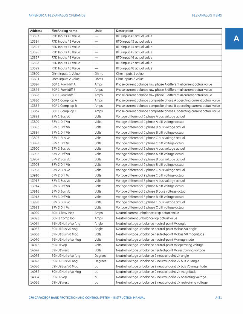
APPENDIX A: FLEXANALOG OPERANDS FLEXANALOG ITEMS
C70 CAPACITOR BANK PROTECTION AND CONTROL SYSTEM – INSTRUCTION MANUAL A-31
A13593 RTD Inputs 42 Value --- RTD input 42 actual value
13594 RTD Inputs 43 Value --- RTD input 43 actual value
13595 RTD Inputs 44 Value --- RTD input 44 actual value
13596 RTD Inputs 45 Value --- RTD input 45 actual value
13597 RTD Inputs 46 Value --- RTD input 46 actual value
13598 RTD Inputs 47 Value --- RTD input 47 actual value
13599 RTD Inputs 48 Value --- RTD input 48 actual value
13600 Ohm Inputs 1 Value Ohms Ohm inputs 1 value
13601 Ohm Inputs 2 Value Ohms Ohm inputs 2 value
13824 60P 1 Raw Idiff A Amps Phase current balance raw phase A differential current actual value
13826 60P 1 Raw Idiff B Amps Phase current balance raw phase B differential current actual value
13828 60P 1 Raw Idiff C Amps Phase current balance raw phase C differential current actual value
13830 60P 1 Comp Iop A Amps Phase current balance composite phase A operating current actual value
13832 60P 1 Comp Iop B Amps Phase current balance composite phase B operating current actual value
13834 60P 1 Comp Iop C Amps Phase current balance composite phase C operating current actual value
13888 87V 1 Bus Va Volts Voltage differential 1 phase A bus voltage actual
13890 87V 1 Diff Va Volts Voltage differential 1 phase A diff voltage actual
13892 87V 1 Diff Vb Volts Voltage differential 1 phase B bus voltage actual
13894 87V 1 Diff Vb Volts Voltage differential 1 phase B diff voltage actual
13896 87V 1 Bus Vc Volts Voltage differential 1 phase C bus voltage actual
13898 87V 1 Diff Vc Volts Voltage differential 1 phase C diff voltage actual
13900 87V 2 Bus Va Volts Voltage differential 2 phase A bus voltage actual
13902 87V 2 Diff Va Volts Voltage differential 2 phase A diff voltage actual
13904 87V 2 Bus Vb Volts Voltage differential 2 phase B bus voltage actual
13906 87V 2 Diff Vb Volts Voltage differential 2 phase B diff voltage actual
13908 87V 2 Bus Vc Volts Voltage differential 2 phase C bus voltage actual
13910 87V 2 Diff Vc Volts Voltage differential 2 phase C diff voltage actual
13912 87V 3 Bus Va Volts Voltage differential 3 phase A bus voltage actual
13914 87V 3 Diff Va Volts Voltage differential 3 phase A diff voltage actual
13916 87V 3 Bus Vb Volts Voltage differential 3 phase B buss voltage actual
13918 87V 3 Diff Vb Volts Voltage differential 3 phase B diff voltage actual
13920 87V 3 Bus Vc Volts Voltage differential 3 phase C bus voltage actual
13922 87V 3 Diff Vc Volts Voltage differential 3 phase C diff voltage actual
14020 60N 1 Raw INsp Amps Neutral current unbalance INsp actual value
14022 60N 1 Comp Iop Amps Neutral current unbalance Iop actual value
14064 59NU1Ntrl-p Vx Ang Angle Neutral voltage unbalance neutral-point Vx angle
14066 59NU1Bus V0 Ang Angle Neutral voltage unbalance neutral-point Vx bus V0 angle
14068 59NU1Bus V0 Mag Volts Neutral voltage unbalance neutral-point Vx bus V0 magnitude
14070 59NU1Ntrl-p Vx Mag Volts Neutral voltage unbalance neutral-point Vx magnitude
14072 59NU1Vop Volts Neutral voltage unbalance neutral-point Vx operating voltage
14074 59NU1Vrest Volts Neutral voltage unbalance neutral-point Vx restraining voltage
14076 59NU2Ntrl-p Vx Ang Degrees Neutral voltage unbalance 2 neutral-point Vx angle
14078 59NU2Bus V0 Ang Degrees Neutral voltage unbalance 2 neutral-point Vx bus V0 angle
14080 59NU2Bus V0 Mag pu Neutral voltage unbalance 2 neutral-point Vx bus V0 magnitude
14082 59NU2Ntrl-p Vx Mag pu Neutral voltage unbalance 2 neutral-point Vx magnitude
14084 59NU2Vop pu Neutral voltage unbalance 2 neutral-point Vx operating voltage
14086 59NU2Vrest pu Neutral voltage unbalance 2 neutral-point Vx restraining voltage
Address FlexAnalog name Units Description
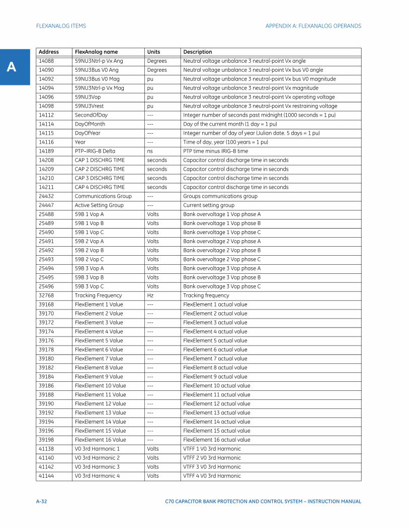
A-32 C70 CAPACITOR BANK PROTECTION AND CONTROL SYSTEM – INSTRUCTION MANUAL
FLEXANALOG ITEMS APPENDIX A: FLEXANALOG OPERANDS
A 14088 59NU3Ntrl-p Vx Ang Degrees Neutral voltage unbalance 3 neutral-point Vx angle
14090 59NU3Bus V0 Ang Degrees Neutral voltage unbalance 3 neutral-point Vx bus V0 angle
14092 59NU3Bus V0 Mag pu Neutral voltage unbalance 3 neutral-point Vx bus V0 magnitude
14094 59NU3Ntrl-p Vx Mag pu Neutral voltage unbalance 3 neutral-point Vx magnitude
14096 59NU3Vop pu Neutral voltage unbalance 3 neutral-point Vx operating voltage
14098 59NU3Vrest pu Neutral voltage unbalance 3 neutral-point Vx restraining voltage
14112 SecondOfDay --- Integer number of seconds past midnight (1000 seconds = 1 pu)
14114 DayOfMonth --- Day of the current month (1 day = 1 pu)
14115 DayOfYear --- Integer number of day of year (Julian date. 5 days = 1 pu)
14116 Year --- Time of day, year (100 years = 1 pu)
14189 PTP–IRIG-B Delta ns PTP time minus IRIG-B time
14208 CAP 1 DISCHRG TIME seconds Capacitor control discharge time in seconds
14209 CAP 2 DISCHRG TIME seconds Capacitor control discharge time in seconds
14210 CAP 3 DISCHRG TIME seconds Capacitor control discharge time in seconds
14211 CAP 4 DISCHRG TIME seconds Capacitor control discharge time in seconds
24432 Communications Group --- Groups communications group
24447 Active Setting Group --- Current setting group
25488 59B 1 Vop A Volts Bank overvoltage 1 Vop phase A
25489 59B 1 Vop B Volts Bank overvoltage 1 Vop phase B
25490 59B 1 Vop C Volts Bank overvoltage 1 Vop phase C
25491 59B 2 Vop A Volts Bank overvoltage 2 Vop phase A
25492 59B 2 Vop B Volts Bank overvoltage 2 Vop phase B
25493 59B 2 Vop C Volts Bank overvoltage 2 Vop phase C
25494 59B 3 Vop A Volts Bank overvoltage 3 Vop phase A
25495 59B 3 Vop B Volts Bank overvoltage 3 Vop phase B
25496 59B 3 Vop C Volts Bank overvoltage 3 Vop phase C
32768 Tracking Frequency Hz Tracking frequency
39168 FlexElement 1 Value --- FlexElement 1 actual value
39170 FlexElement 2 Value --- FlexElement 2 actual value
39172 FlexElement 3 Value --- FlexElement 3 actual value
39174 FlexElement 4 Value --- FlexElement 4 actual value
39176 FlexElement 5 Value --- FlexElement 5 actual value
39178 FlexElement 6 Value --- FlexElement 6 actual value
39180 FlexElement 7 Value --- FlexElement 7 actual value
39182 FlexElement 8 Value --- FlexElement 8 actual value
39184 FlexElement 9 Value --- FlexElement 9 actual value
39186 FlexElement 10 Value --- FlexElement 10 actual value
39188 FlexElement 11 Value --- FlexElement 11 actual value
39190 FlexElement 12 Value --- FlexElement 12 actual value
39192 FlexElement 13 Value --- FlexElement 13 actual value
39194 FlexElement 14 Value --- FlexElement 14 actual value
39196 FlexElement 15 Value --- FlexElement 15 actual value
39198 FlexElement 16 Value --- FlexElement 16 actual value
41138 V0 3rd Harmonic 1 Volts VTFF 1 V0 3rd Harmonic
41140 V0 3rd Harmonic 2 Volts VTFF 2 V0 3rd Harmonic
41142 V0 3rd Harmonic 3 Volts VTFF 3 V0 3rd Harmonic
41144 V0 3rd Harmonic 4 Volts VTFF 4 V0 3rd Harmonic
Address FlexAnalog name Units Description

APPENDIX A: FLEXANALOG OPERANDS FLEXANALOG ITEMS
C70 CAPACITOR BANK PROTECTION AND CONTROL SYSTEM – INSTRUCTION MANUAL A-33
A41146 V0 3rd Harmonic 5 Volts VTFF 5 V0 3rd Harmonic
41148 V0 3rd Harmonic 6 Volts VTFF 6 V0 3rd Harmonic
45584 RxGOOSE Analog1 --- RxGOOSE analog input 1
45586 RxGOOSE Analog2 --- RxGOOSE analog input 2
45588 RxGOOSE Analog3 --- RxGOOSE analog input 3
45590 RxGOOSE Analog4 --- RxGOOSE analog input 4
45592 RxGOOSE Analog5 --- RxGOOSE analog input 5
45594 RxGOOSE Analog6 --- RxGOOSE analog input 6
45596 RxGOOSE Analog7 --- RxGOOSE analog input 7
45598 RxGOOSE Analog8 --- RxGOOSE analog input 8
45600 RxGOOSE Analog9 --- RxGOOSE analog input 9
45602 RxGOOSE Analog10 --- RxGOOSE analog input 10
45604 RxGOOSE Analog11 --- RxGOOSE analog input 11
45606 RxGOOSE Analog12 --- RxGOOSE analog input 12
45608 RxGOOSE Analog13 --- RxGOOSE analog input 13
45610 RxGOOSE Analog14 --- RxGOOSE analog input 14
45612 RxGOOSE Analog15 --- RxGOOSE analog input 15
45614 RxGOOSE Analog16 --- RxGOOSE analog input 16
45616 RxGOOSE Analog17 --- RxGOOSE analog input 17
45618 RxGOOSE Analog18 --- RxGOOSE analog input 18
45620 RxGOOSE Analog19 --- RxGOOSE analog input 19
45622 RxGOOSE Analog20 --- RxGOOSE analog input 20
45624 RxGOOSE Analog21 --- RxGOOSE analog input 21
45626 RxGOOSE Analog22 --- RxGOOSE analog input 22
45628 RxGOOSE Analog23 --- RxGOOSE analog input 23
45630 RxGOOSE Analog24 --- RxGOOSE analog input 24
45632 RxGOOSE Analog25 --- RxGOOSE analog input 25
45634 RxGOOSE Analog26 --- RxGOOSE analog input 26
45636 RxGOOSE Analog27 --- RxGOOSE analog input 27
45638 RxGOOSE Analog28 --- RxGOOSE analog input 28
45640 RxGOOSE Analog29 --- RxGOOSE analog input 29
45642 RxGOOSE Analog30 --- RxGOOSE analog input 30
45644 RxGOOSE Analog31 --- RxGOOSE analog input 31
45646 RxGOOSE Analog32 --- RxGOOSE analog input 32
Address FlexAnalog name Units Description

A-34 C70 CAPACITOR BANK PROTECTION AND CONTROL SYSTEM – INSTRUCTION MANUAL
FLEXANALOG ITEMS APPENDIX A: FLEXANALOG OPERANDS
A
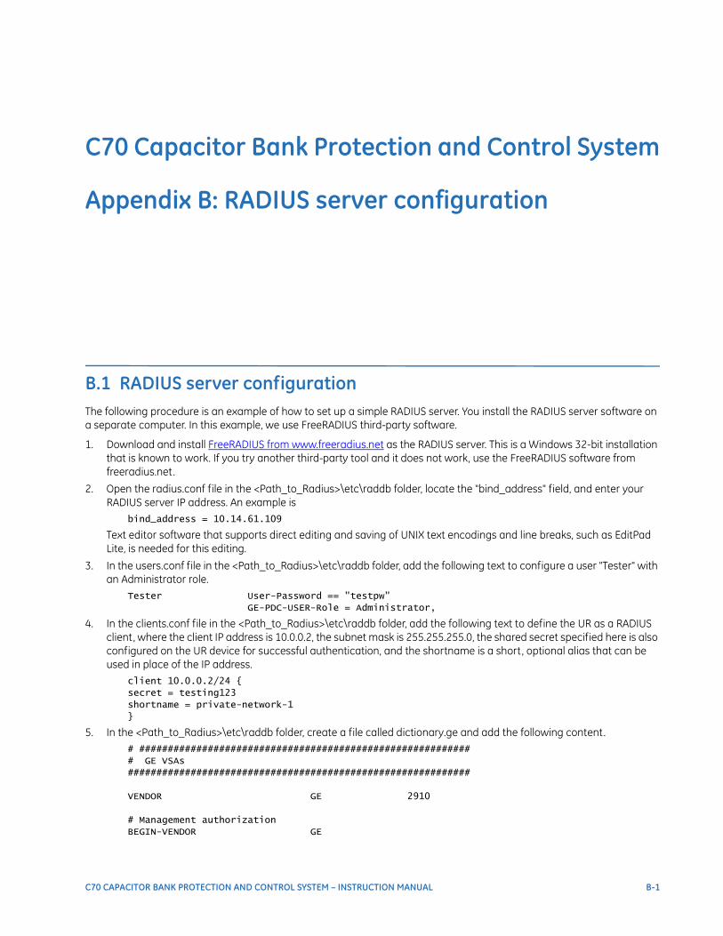
C70 CAPACITOR BANK PROTECTION AND CONTROL SYSTEM – INSTRUCTION MANUAL B-1
C70 Capacitor Bank Protection and Control System
Appendix B: RADIUS server configuration
RADIUS server configuration
B.1 RADIUS server configurationThe following procedure is an example of how to set up a simple RADIUS server. You install the RADIUS server software on a separate computer. In this example, we use FreeRADIUS third-party software.
1. Download and install FreeRADIUS from www.freeradius.net as the RADIUS server. This is a Windows 32-bit installation that is known to work. If you try another third-party tool and it does not work, use the FreeRADIUS software from freeradius.net.
2. Open the radius.conf file in the <Path_to_Radius>\etc\raddb folder, locate the "bind_address" field, and enter your RADIUS server IP address. An example is
bind_address = 10.14.61.109
Text editor software that supports direct editing and saving of UNIX text encodings and line breaks, such as EditPad Lite, is needed for this editing.
3. In the users.conf file in the <Path_to_Radius>\etc\raddb folder, add the following text to configure a user "Tester" with an Administrator role.
Tester User-Password == "testpw"
GE-PDC-USER-Role = Administrator,
4. In the clients.conf file in the <Path_to_Radius>\etc\raddb folder, add the following text to define the UR as a RADIUS client, where the client IP address is 10.0.0.2, the subnet mask is 255.255.255.0, the shared secret specified here is also configured on the UR device for successful authentication, and the shortname is a short, optional alias that can be used in place of the IP address.
client 10.0.0.2/24
secret = testing123
shortname = private-network-1
5. In the <Path_to_Radius>\etc\raddb folder, create a file called dictionary.ge and add the following content.# ########################################################### GE VSAs
############################################################
VENDOR GE 2910
# Management authorizationBEGIN-VENDOR GE
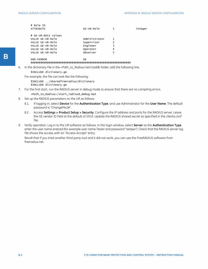
B-2 C70 CAPACITOR BANK PROTECTION AND CONTROL SYSTEM – INSTRUCTION MANUAL
RADIUS SERVER CONFIGURATION APPENDIX B: RADIUS SERVER CONFIGURATION
B
# Role IDATTRIBUTE GE-UR-Role 1 integer
# GE-UR-ROLE valuesVALUE GE-UR-Role Administrator 1
VALUE GE-UR-Role Supervisor 2
VALUE GE-UR-Role Engineer 3VALUE GE-UR-Role Operator 4
VALUE GE-UR-Role Observer 5
END-VENDOR GE
#############################################################
6. In the dictionary file in the <Path_to_Radius>\etc\raddb folder, add the following line.$INCLUDE dictionary.ge
For example, the file can look like the following:$INCLUDE ../shareéfreeradius/dictionary$INCLUDE dictionary.ge
7. For the first start, run the RADIUS server in debug mode to ensure that there are no compiling errors.<Path_to_Radius>/start_radiusd_debug.bat
8. Set up the RADIUS parameters on the UR as follows.
8.1. If logging in, select Device for the Authentication Type, and use Administrator for the User Name. The default password is "ChangeMe1#".
8.2. Access Settings > Product Setup > Security. Configure the IP address and ports for the RADIUS server. Leave the GE vendor ID field at the default of 2910. Update the RADIUS shared secret as specified in the clients.conf file.
9. Verify operation. Log in to the UR software as follows. In the login window, select Server as the Authentication Type, enter the user name entered (for example user name Tester and password "testpw"). Check that the RADIUS server log file shows the access with an "Access-Accept" entry.
Recall that If you tried another third-party tool and it did not work, you can use the FreeRADIUS software from freeradius.net.

C70 CAPACITOR BANK PROTECTION AND CONTROL SYSTEM – INSTRUCTION MANUAL C-1
C70 Capacitor Bank Protection and Control System
Appendix C: Miscellaneous
Miscellaneous
This chapter provides the warranty and revision history.
C.1 WarrantyFor products shipped as of 1 October 2013, GE Digital Energy warrants most of its GE manufactured products for 10 years. For warranty details including any limitations and disclaimers, see the GE Digital Energy Terms and Conditions at https://www.gedigitalenergy.com/multilin/warranty.htm
For products shipped before 1 October 2013, the standard 24-month warranty applies.
C.2 Revision historyThe tables outline the releases and revision history of this document.
Table C-1: Revision history (English)
Manual P/N C70 revision Release date ECO
1601-9015-P1 5.2x 23 October 2006 URX-230
1601-9015-P2 5.2x 24 January 2007 URX-232
1601-9015-R1 5.4x 26 June 2007 URX-242
1601-9015-R2 5.4x 31 August 2007 URX-246
1601-9015-R3 5.4x 17 October 2007 URX-251
1601-9015-S1 5.5x 7 December 2007 URX-253
1601-9015-S2 5.5x 22 February 2008 URX-258
1601-9015-S3 5.5x 12 March 2008 URX-260
1601-9015-T1 5.6x 27 June 2008 08-0390
1601-9015-U1 5.7x 29 May 2009 09-0938
1601-9015-U2 5.7x 30 September 2009 09-1165
1601-9015-V1 5.8x 29 May 2010 09-1457
1601-9015-V2 5.8x 04 January 2011 11-2237
1601-9015-W1 5.9x 12 January 2011 11-2227
1601-9015-X1 6.0x 21 December 2011 11-2840

C-2 C70 CAPACITOR BANK PROTECTION AND CONTROL SYSTEM – INSTRUCTION MANUAL
REVISION HISTORY APPENDIX C: MISCELLANEOUS
CTable C-2: Major changes for C70 manual version AB2 (English)
Table C-3: Major changes for C70 manual version AB1 (English)
Table C-4: Major changes for C70 manual version AA1 (English)
1601-9015-X2 6.0x 5 April 2012 12-3254
1601-9015-Y1 7.0x 30 September 2012 12-3529
1601-9015-Y2 7.0x 11 November 2012 12-3601
1601-9015-Z1 7.1x 30 March 2013 13-0126
1601-9015-AA1 7.2x 1 August 2013 13-0401
1601-9015-AB1 7.3x 7 November 2014 14-1408
1601-9015-AB2 7.3x 1 September 2015 15-2215
Page Description
--- Updated document throughout, including numbers of elements and FlexLogic operands table
--- Added EAC compliance information throughout, including logo on title page, rear panel, added specifications, added life expectancy and decommissioning, added sections on Repairs, Storage, and Disposal
--- Updated several figures for consistency
2-15 Added UR Signal Processing section
5- Updated IEC 61850 content
A- Updated FlexAnalog table
Page Description
--- Updated document throughout and put into new template. Major revision.
--- Updated references to digital inputs/outputs to contact inputs/outputs for consistency
--- Added content for advanced IEC 61850, for example in the Settings and Actual Values chapters
2- Updated Order Codes and Specifications
5-28 Added RS232 Baud Rate setting to Serial Ports section. Baud rate is now configurable, with two options.
5-32 Added Far-End Fault Indication (FEFI) section
5-56 Deleted Ethernet Global Data (EGD) settings, which do not apply to the C70
9-2 Added Software Upgrade section to the Maintenance chapter
--- Moved communications appendices B through F to new UR Series Communications Guide for UR 7.3x AB1
C-1 Updated product warranty from 24 months to 10 years
Page (Z1)
Page (AA1)
Change Description
--- --- Add Added content for IEC 60870-5-103 throughout document
2- 2- Update Updated order codes
2- 2- Update Updated specifications
8- --- Delete Deleted chapter 8 on security, moving content to other chapters
--- 10- Add Added Maintenance chapter, moving content from other chapters and adding new instructions to replace the battery
--- D- Add Added new appendix on IEC 60870-5-103 interoperability
Manual P/N C70 revision Release date ECO

C70 CAPACITOR BANK PROTECTION AND CONTROL SYSTEM – INSTRUCTION MANUAL i
C70 Capacitor Bank Protection and Control System
Abbreviations
Abbreviations
A AmpereAC Alternating CurrentA/D Analog to DigitalAE Accidental Energization, Application EntityAMP AmpereANG AngleANSI American National Standards InstituteAR Automatic ReclosureASDU Application-layer Service Data UnitASYM AsymmetryAUTO AutomaticAUX AuxiliaryAVG AverageAWG American Wire Gauge
BCS Best Clock SelectorBER Bit Error RateBF Breaker FailBFI Breaker Failure InitiateBKR BreakerBLK BlockBLKG BlockingBNC Bayonet Neill-ConcelmanBPNT Breakpoint of a characteristicBRKR Breaker
CAP CapacitorCC Coupling CapacitorCCVT Coupling Capacitor Voltage TransformerCFG Configure / Configurable.CFG Filename extension for oscillography filesCHK CheckCHNL ChannelCID Configured IED DescriptionCLS CloseCLSD ClosedCMND CommandCMPRSN ComparisonCO Contact OutputCOM CommunicationCOMM CommunicationsCOMP Compensated, ComparisonCONN ConnectionCONT Continuous, ContactCO-ORD CoordinationCPU Central Processing UnitCRC Cyclic Redundancy Code/Check
CRT, CRNT CurrentCSA Canadian Standards AssociationCT Current TransformerCVT Capacitive Voltage Transformer
D/A Digital to AnalogDC (dc) Direct CurrentDCE Data Communications EquipmentDCS Distributed Control SystemDD Disturbance DetectorDFLT DefaultDGNST DiagnosticsDIFF DifferentialDIR DirectionalDISCREP DiscrepancyDIST DistanceDMD DemandDNP Distributed Network ProtocolDPO DropoutDSP Digital Signal ProcessorDST Daylight Savings Timedt Rate of ChangeDTT Direct Transfer TripDUTT Direct Under-reaching Transfer Trip
EGD Ethernet Global DataENCRMNT EncroachmentEPRI Electric Power Research Institute.EVT Filename extension for event recorder filesEXT Extension, External
F FieldFAIL FailureFD Fault DetectorFDH Fault Detector high-setFDL Fault Detector low-setFLA Full Load CurrentFO Fiber OpticFREQ FrequencyFSK Frequency-Shift KeyingFTP File Transfer ProtocolFxE FlexElement™FWD Forward
G GeneratorGE General ElectricGND GroundGNTR Generator
Glossary

ii C70 CAPACITOR BANK PROTECTION AND CONTROL SYSTEM – INSTRUCTION MANUAL
ABBREVIATIONS
GOOSE General Object Oriented Substation EventGPS Global Positioning SystemGSU Generator Step-Up
HARM Harmonic / HarmonicsHCT High Current TimeHGF High-Impedance Ground Fault (CT)HIZ High-Impedance and Arcing GroundHMI Human-Machine InterfaceHTTP Hyper Text Transfer ProtocolHV High VoltageHYB HybridHz Hertz
I InstantaneousI_0 Zero Sequence currentI_1 Positive Sequence currentI_2 Negative Sequence currentIA Phase A currentIAB Phase A minus B currentIB Phase B currentIBC Phase B minus C currentIC Phase C currentICA Phase C minus A currentID IdentificationIED Intelligent Electronic DeviceIEC International Electrotechnical CommissionIEEE Institute of Electrical and Electronic EngineersIG Ground (not residual) currentIgd Differential Ground currentIN CT Residual Current (3Io) or InputINC SEQ Incomplete SequenceINIT InitiateINST InstantaneousINV InverseI/O Input/OutputIOC Instantaneous OvercurrentIOV Instantaneous OvervoltageIRIG Inter-Range Instrumentation GroupISO International Standards OrganizationIUV Instantaneous Undervoltage
K0 Zero Sequence Current CompensationkA kiloAmperekV kiloVolt
LED Light Emitting DiodeLEO Line End OpenLFT BLD Left BlinderLOOP LoopbackLPU Line PickupLRA Locked-Rotor CurrentLTC Load Tap-ChangerLV Low Voltage
M MachinemA MilliAmpereMAG MagnitudeMAN Manual / ManuallyMAX MaximumMIC Model Implementation ConformanceMIN Minimum, MinutesMMI Man Machine InterfaceMMS Manufacturing Message SpecificationMRT Minimum Response TimeMSG MessageMTA Maximum Torque AngleMTR MotorMVA MegaVolt-Ampere (total 3-phase)MVA_A MegaVolt-Ampere (phase A)MVA_B MegaVolt-Ampere (phase B)MVA_C MegaVolt-Ampere (phase C)
MVAR MegaVar (total 3-phase)MVAR_A MegaVar (phase A)MVAR_B MegaVar (phase B)MVAR_C MegaVar (phase C)MVARH MegaVar-HourMW MegaWatt (total 3-phase)MW_A MegaWatt (phase A)MW_B MegaWatt (phase B)MW_C MegaWatt (phase C)MWH MegaWatt-Hour
N NeutralN/A, n/a Not ApplicableNEG NegativeNMPLT NameplateNOM NominalNTR Neutral
O OverOC, O/C OvercurrentO/P, Op OutputOP OperateOPER OperateOPERATG OperatingO/S Operating SystemOSI Open Systems InterconnectOSB Out-of-Step BlockingOUT OutputOV OvervoltageOVERFREQ OverfrequencyOVLD Overload
P PhasePC Phase Comparison, Personal ComputerPCNT PercentPF Power Factor (total 3-phase)PF_A Power Factor (phase A)PF_B Power Factor (phase B)PF_C Power Factor (phase C)PFLL Phase and Frequency Lock LoopPHS PhasePICS Protocol Implementation & Conformance
StatementPKP PickupPLC Power Line CarrierPOS PositivePOTT Permissive Over-reaching Transfer TripPRESS PressurePRI PrimaryPROT ProtectionPSEL Presentation Selectorpu Per UnitPUIB Pickup Current BlockPUIT Pickup Current TripPUSHBTN PushbuttonPUTT Permissive Under-reaching Transfer TripPWM Pulse Width ModulatedPWR Power
QUAD Quadrilateral
R Rate, ReverseRCA Reach Characteristic AngleREF ReferenceREM RemoteREV ReverseRI Reclose InitiateRIP Reclose In ProgressRGT BLD Right BlinderRMA Return Materials AuthorizationRMS Root Mean SquareROCOF Rate of Change of Frequency

ABBREVIATIONS
C70 CAPACITOR BANK PROTECTION AND CONTROL SYSTEM – INSTRUCTION MANUAL iii
ROD Remote Open DetectorRST ResetRSTR RestrainedRTD Resistance Temperature DetectorRTU Remote Terminal UnitRX (Rx) Receive, Receiver
s secondS SensitiveSAT CT SaturationSBO Select Before OperateSCADA Supervisory Control and Data AcquisitionSCC Serial Communication ControllerSCL Substation Configuration LanguageSEC SecondarySEL Select / Selector / SelectionSENS SensitiveSEQ SequenceSIR Source Impedance RatioSNTP Simple Network Time ProtocolSRC SourceSSB Single Side BandSSEL Session SelectorSTATS StatisticsSUPN SupervisionSUPV Supervise / SupervisionSV Supervision, ServiceSYNC SynchrocheckSYNCHCHK Synchrocheck
T Time, transformerTC Thermal CapacityTCP Transmission Control ProtocolTCU Thermal Capacity UsedTD MULT Time Dial MultiplierTEMP TemperatureTFTP Trivial File Transfer ProtocolTHD Total Harmonic DistortionTMR TimerTOC Time OvercurrentTOV Time OvervoltageTRANS TransientTRANSF TransferTSEL Transport SelectorTUC Time UndercurrentTUV Time UndervoltageTX (Tx) Transmit, Transmitter
U UnderUC UndercurrentUCA Utility Communications ArchitectureUDP User Datagram ProtocolUL Underwriters LaboratoriesUNBAL UnbalanceUR Universal RelayURC Universal Recloser Control.URS Filename extension for settings filesUV Undervoltage
V/Hz Volts per hertzV_0 Zero Sequence voltageV_1 Positive Sequence voltageV_2 Negative Sequence voltageVA Phase A voltageVAB Phase A to B voltageVAG Phase A to Ground voltageVARH Var-hour voltageVB Phase B voltageVBA Phase B to A voltageVBG Phase B to Ground voltageVC Phase C voltageVCA Phase C to A voltage
VCG Phase C to Ground voltageVF Variable FrequencyVIBR VibrationVT Voltage TransformerVTFF Voltage Transformer Fuse FailureVTLOS Voltage Transformer Loss Of Signal
WDG WindingWH Watt-hourw/ opt With OptionWGS World Geodetic SystemWRT With Respect To
X ReactanceXDUCER TransducerXFMR Transformer
Z Impedance, Zone

iv C70 CAPACITOR BANK PROTECTION AND CONTROL SYSTEM – INSTRUCTION MANUAL
ABBREVIATIONS
C70 CAPACITOR BANK PROTECTION AND CONTROL SYSTEM – INSTRUCTION MANUAL i
C70 Capacitor Bank Protection and Control System
Index
Index
Numerics10BASE-F settings ...............................................................................5-31
AAC current input specifications ...................................................2-25AC current inputs ..............................................................................5-112AC inputs ...................................................................................................3-11AC voltage input specifications ...................................................2-25Access Violation message ..............................................................3-42Active setting group ........................................................................5-156Actual values ............................................................................................ 6-1Administrator
add user account ..............................................................................5-13command to force logoff ................................................................ 7-8role for CyberSentry .......................................................................... 2-5
Alarm LEDs ..............................................................................................5-93ANSI device numbers .......................................................................... 2-2Apparent power ....................................................................................6-15Apparent power specifications ....................................................2-24Application examples
breaker trip circuit integrity ......................................................5-240contact inputs .................................................................................5-256direct inputs and outputs ..........................................................5-262latching outputs .............................................................................5-259
Approvals .................................................................................................2-33Architecture, relay ............................................................................5-132Authentication by device or server ...........................................5-15Automatic discovery of UR devices ...........................................3-42Automatic voltage regulator
FlexLogic operands .......................................................................5-134logic diagram ...................................................................................5-237settings ...............................................................................................5-233specifications ......................................................................................2-17
Auxiliary overvoltageFlexLogic operands .......................................................................5-134logic ......................................................................................................5-206settings ...............................................................................................5-205specifications ..................................................................................... 2-21
Auxiliary voltage channel ............................................................... 3-12Auxiliary voltage metering ............................................................. 6-15AWG wire size ................................................................ 3-11, 3-28, 3-31
BBack up settings ...................................................................... 5-45, 10-2Bank phase overvoltage
FlexLogic operands .......................................................................5-135logic diagram ...................................................................................5-213settings ...............................................................................................5-209specifications ..................................................................................... 2-20theory of operation ............................................................................9-1
Banks ................................................................................5-6, 5-112, 5-113Battery
disposal ................................................................................................. 10-9failure message ................................................................................ 7-11replace .................................................................................................. 10-7
Baud rate ................................................................................................. 5-28BLOCK setting ..........................................................................................5-5Breaker control
control of two breakers ................................................................. 4-25dual breaker logic ..........................................................................5-120FlexLogic operands .......................................................................5-136settings ...............................................................................................5-117

ii C70 CAPACITOR BANK PROTECTION AND CONTROL SYSTEM – INSTRUCTION MANUAL
INDEX
Breaker failuredescription ........................................................................................5-192determination ..................................................................................5-193FlexLogic operands .......................................................................5-135logic diagram .................................................................... 5-196, 5-197main path sequence ....................................................................5-193settings ................................................................................ 5-191, 5-194specifications ..................................................................................... 2-21
Breaker flashoverFlexLogic operands .......................................................................5-135logic diagram ...................................................................................5-247settings ...............................................................................................5-242specifications ..................................................................................... 2-21
Breaker restrikeFlexLogic operands .......................................................................5-135logic diagram ...................................................................................5-250settings ...............................................................................................5-248
Breaker-and-a-half scheme ............................................................ 5-5Brightness ............................................................................................... 5-25
CC37.94 communications ................................................................. 3-34Capacitor control
FlexLogic operands .......................................................................5-136logic diagram ...................................................................................5-232settings ...............................................................................................5-228specifications ..................................................................................... 2-17
CE certification ..................................................................................... 2-33Certification ............................................................................................ 2-33Changes ......................................................................................................C-1Channel
banks .................................................................................... 5-112, 5-113CID files ..................................................................................................... 5-45Circuit monitoring applications ................................................5-238Cleaning ................................................................................................... 2-33Clear
files and records .............................................................................10-12LEDs ......................................................................................................5-260relay records using settings ........................................................ 5-27security logs .......................................................................................... 7-8
Clockactual values ......................................................................................... 6-6IRIG-B ..................................................................................................... 3-24PTP .......................................................................................................... 5-83set on front panel ............................................................................... 7-7settings ................................................................................................. 5-82time of day specifications ............................................................ 2-23
CloseHTTP port ............................................................................................. 5-74IEC 60870-5-104 port .................................................................... 5-76Modbus port ....................................................................................... 5-37SNTP port ............................................................................................. 5-85TFTP port .............................................................................................. 5-75Web access ........................................................................................ 5-74Web access port .............................................................................. 5-74
Comm status remaining connections ....................................... 6-8
Command password ................................................................4-26, 5-9Commands
control user accounts .................................................................... 5-13menu .........................................................................................................7-1
Communications10BASE-F .............................................................................................. 5-31connecting to the UR .......................................................... 3-41, 3-42DNP ......................................................................................................... 5-38HTTP ........................................................................................................ 5-74IEC 60870-5-10 ................................................................................. 5-77IEC 60870-5-104 ............................................................................... 5-75inter-relay specifications .............................................................. 2-30Modbus registers .............................................................................. 5-82Modbus settings ............................................................................... 5-36RS232 ......................................................................................... 3-22, 5-28RS485 ......................................................................................... 3-23, 5-28settings ...................................................................................... 5-31, 5-38specifications ......................................................................... 2-29, 2-30web server ........................................................................................... 5-74
Compliance ............................................................................................. 2-33Conducted RFI specifications ....................................................... 2-32Contact inputs
actual values .........................................................................................6-3explained ........................................................................................... 5-255FlexLogic operands ...................................................................... 5-142settings ............................................................................................... 5-254specifications ..................................................................................... 2-25thresholds ......................................................................................... 5-255wet and dry connections .............................................................. 3-19
Contact outputsactual values .........................................................................................6-4explained ........................................................................................... 5-257FlexLogic operands ...................................................................... 5-142settings ............................................................................................... 5-257
Control elements .............................................................................. 5-217Control power
description ........................................................................................... 3-10specifications ..................................................................................... 2-28
Control pushbuttonsFlexLogic operands ...................................................................... 5-134logic diagram ..................................................................................... 5-95settings .................................................................................................. 5-94specifications ..................................................................................... 2-23
Countersactual values .........................................................................................6-5settings ............................................................................................... 5-240
CRC alarm ............................................................................................. 5-110Critical failure relay specifications ............................................ 2-27CSA certification ................................................................................... 2-33CT bank settings ............................................................................... 5-112CT inputs ...........................................................................3-11, 5-6, 5-112CT wiring ................................................................................................... 3-12Current bank ....................................................................................... 5-112Current harmonics specifications ............................................. 2-24Current metering actual values .................................................. 6-13

INDEX
C70 CAPACITOR BANK PROTECTION AND CONTROL SYSTEM – INSTRUCTION MANUAL iii
Curvesdefinite time ...................................................................... 5-162, 5-201FlexCurves .......................................................................... 5-125, 5-162IAC .........................................................................................................5-160IEC .........................................................................................................5-159IEEE .......................................................................................................5-158inverse time undervoltage ........................................................5-201types ....................................................................................................5-157
Cutout, panel ...................................................................................3-2, 3-3CyberSentry
FlexLogic operands .......................................................................5-134installation ...............................................................................3-49, 5-23security commands ........................................................................... 7-8security overview ................................................................................ 2-4system logs ..........................................................................................5-24
DData logger
actual values .......................................................................................6-21clearing ........................................................................................ 5-27, 7-6settings ..................................................................................................5-89specifications ......................................................................................2-24
Data, reading values ............................................................................ 6-1Date, set ...................................................................................................... 7-7DCmA inputs ...........................................................................................6-20
actual values .......................................................................................6-20settings ...............................................................................................5-265specifications ......................................................................................2-25
DCmA outputsdescription ...........................................................................................3-21settings ...............................................................................................5-267specifications ......................................................................................2-28
Decommission ....................................................................................10-12Default password ................................................................................5-13Default settings .....................................................................................10-2Definite time curve ............................................................ 5-162, 5-201Delete files and records ....................................................5-27, 10-12Device authentication .......................................................................5-15Device setup ...........................................................................................3-42Dielectric strength ...............................................................................3-10Digital counters
actual values ......................................................................................... 6-5FlexLogic operands .......................................................................5-136logic diagram ...................................................................................5-242settings ...............................................................................................5-240
Digital elementsapplication example .....................................................................5-239FlexLogic operands .......................................................................5-137logic diagram ...................................................................................5-238settings ...............................................................................................5-237
Digital outputssee Contact outputs
Dimensions .......................................................................................3-2, 3-3Direct devices
settings ...............................................................................................5-261status ........................................................................................................ 6-8
Direct I/Oapplication example .....................................................................5-262configuration examples ..............................................................5-106error messages ................................................................................. 7-11settings ...............................................................................................5-261
Direct inputsactual values .........................................................................................6-7application example .....................................................................5-262clearing counters ................................................................................7-6error messages ................................................................................. 7-11FlexLogic operands .......................................................................5-142settings ...............................................................................................5-261specifications ..................................................................................... 2-26
Direct outputsapplication example .....................................................................5-262clearing counters ................................................................................7-6error messages ................................................................................. 7-11settings ...............................................................................................5-261
Directional overcurrentsee Phase, Ground, and Neutral directional
Directional polarization .................................................................5-165Disconnect switch
FlexLogic operands .......................................................................5-141logic ......................................................................................................5-124settings ...............................................................................................5-122
Discover button .................................................................................... 3-42Display settings .................................................................................... 5-25Disposal ..................................................................................................10-13Dispose of battery .............................................................................. 10-9Disturbance detector
FlexLogic operands .......................................................................5-140internal ................................................................................................5-115
DNPconnections remaining ....................................................................6-8settings ................................................................................................. 5-38
Drag and drop files ...............................................................................4-2
EEAC certification ................................................................................... 2-33Electrostatic discharge specifications .................................... 2-32Elements ......................................................................................................5-4End of life ...............................................................................................10-13EnerVista UR setup
drag and drop files .............................................................................4-2event recorder ......................................................................................4-2firmware upgrades .......................................................................... 10-4installation ........................................................................................... 3-38oscillography .........................................................................................4-2requirements ...................................................................................... 3-38restart relay ........................................................................................ 5-45
Engineer command to force logoff .............................................7-8

iv C70 CAPACITOR BANK PROTECTION AND CONTROL SYSTEM – INSTRUCTION MANUAL
INDEX
Equationsdefinite time curve ......................................................... 5-162, 5-201FlexCurves .........................................................................................5-162FlexLogic ............................................................................................5-151FlexLogic, protect ................................................................................ 4-8IAC curves ..........................................................................................5-160IEC curves ..........................................................................................5-159IEEE curves ........................................................................................5-158
Equipment mismatch error ........................................................... 7-10Error messages ....................................................................................... 7-9
order code mismatch .................................................................... 10-5Ethernet
actual values ......................................................................................... 6-6configuration ..................................................................................... 3-41error messages ................................................................................. 7-12Quick Connect ................................................................................... 3-44settings ................................................................................................. 5-31
Event cause indicators .................................................................... 4-17Event Cause LEDs ............................................................................... 4-19Event recorder
actual values ...................................................................................... 6-20clearing ........................................................................................ 5-27, 7-6specifications ..................................................................................... 2-23via EnerVista software ...................................................................... 4-2
EVENTS setting ........................................................................................ 5-5Export settings to file ........................................................................ 10-2
FF485 ............................................................................................................ 3-37Faceplate ........................................................................................ 3-2, 4-15Factory default reset ............................................................... 5-7, 5-21Far-End Fault Indication ................................................................. 5-32Fast form-C relay specifications ................................................ 2-27Fast transient testing specifications ........................................ 2-32Features ...................................................................................................... 2-1Fiber signal loss detection ............................................................. 5-32File transfer by IEC 61850 .............................................................. 5-74File transfer by TFTP .......................................................................... 5-75Files
delete ...................................................................................................10-12drag and drop ...................................................................................... 4-2protect FlexLogic with password ................................................ 4-8protect with password ..................................................................... 4-5transfer to relay ................................................................................... 4-1
Firmware revision ............................................................................... 6-22Firmware upgrades ........................................................................... 10-4Firmware version does not match EnerVista ..................... 10-5Flash memory .....................................................................................10-12Flash messages ................................................................................... 5-25Flex State parameters
actual values ......................................................................................... 6-6settings ...............................................................................................5-101specifications ..................................................................................... 2-22
FlexAnalog parameters ......................................................................A-1
FlexCurvesequation ............................................................................................ 5-162settings ............................................................................................... 5-125specifications ..................................................................................... 2-22table ..................................................................................................... 5-125
FlexElementsactual values ...................................................................................... 6-19direction ............................................................................................. 5-153FlexLogic operands ...................................................................... 5-137hysteresis .......................................................................................... 5-153logic diagram .................................................................................. 5-152pickup ................................................................................................. 5-153settings ............................................................................................... 5-151specifications ..................................................................................... 2-22
FlexLogicedit with equation editor ........................................................... 5-151equation editor ............................................................................... 5-151equation example ......................................................................... 5-220error messages ................................................................................. 7-10evaluation ......................................................................................... 5-145example ............................................................................................. 5-146gate characteristics ..................................................................... 5-144lock equations ......................................................................................4-8lock equations to serial number ..................................................4-9operands ........................................................................................... 5-134operators ........................................................................................... 5-144rules ..................................................................................................... 5-145security .....................................................................................................4-8specifications ..................................................................................... 2-22timer settings .................................................................................. 5-151worksheet ......................................................................................... 5-148
Force contact inputs ...................................................................... 5-272Force contact outputs ................................................................... 5-272Form-A
actual values .........................................................................................6-4Form-A relay
high-impedance circuits ............................................................... 3-14outputs .................................................................................................. 3-13specifications ..................................................................................... 2-27
Form-Cactual values .........................................................................................6-4critical failure relay .......................................................................... 3-10order codes ............................................................................................2-7outputs .................................................................................................. 3-13replacement modules .................................................................... 2-12specifications ..................................................................................... 2-27
Frequency meteringactual values ...................................................................................... 6-16specifications ..................................................................................... 2-24
Frequency tracking ............................................................................ 6-19Frequency, nominal ........................................................................ 5-114

INDEX
C70 CAPACITOR BANK PROTECTION AND CONTROL SYSTEM – INSTRUCTION MANUAL v
Front panelclear .....................................................................................................5-260custom labels .....................................................................................4-20interface ................................................................................................4-12LEDs ........................................................................................................4-17password change .............................................................................4-26use ...........................................................................................................4-12variations ..............................................................................................4-15
FUNCTION setting .................................................................................. 5-4Fuse failure ...........................................................................................5-250Fuse specifications .............................................................................2-26
GG.703 ...........................................................................................................3-27
wire size .................................................................................................3-28Gateway address .................................................................................5-34GE type IAC curves ...........................................................................5-160Getting help ............................................................................................... 1-2GOOSE
actual values .......................................................................................6-19error messages ..................................................................................7-12settings ..................................................................................................5-48
Ground current metering ................................................................6-14Ground IOC
FlexLogic operands .......................................................................5-137logic diagram ...................................................................................5-185settings ...............................................................................................5-184
Ground TOCFlexLogic operands .......................................................................5-137logic diagram ...................................................................................5-184settings ...............................................................................................5-183specifications ......................................................................................2-17
Group 1 switch after powerup ..................................................5-156Grouped elements ...........................................................................5-156Guarantee ..................................................................................................C-1
HHardFiber
interface module described .........................................................3-13order codes for compatible URs .................................................. 2-7self-test errors ....................................................................................7-14
Harmonic content ...................................................................6-16, 6-17Harmonics
actual values ...........................................................................6-16, 6-17Harmonics metering
specifications ......................................................................................2-24Heartbeat messages .............................................................5-49, 5-51HTTP ............................................................................................................5-74
port, close .............................................................................................5-74Humidity specifications ....................................................................2-31Hysteresis ..............................................................................................5-153
IIAC curves ..............................................................................................5-160IEC 60870-5-103 protocol
explained .............................................................................................. 5-77settings ................................................................................................. 5-77
IEC 60870-5-104 protocolconnections remaining ....................................................................6-8port, close ............................................................................................ 5-76settings ................................................................................................. 5-75
IEC 61850 protocolcompatibility with previous release ........................................ 5-43error messages ................................................................................. 7-12explained .............................................................................................. 5-43file transfer .......................................................................................... 5-74heartbeat messages .......................................................... 5-49, 5-51IID file ..................................................................................................... 10-2settings in EnerVista ....................................................................... 5-42specifications ..................................................................................... 2-29
IEC CID files ............................................................................................. 5-45IED setup .................................................................................................. 3-38IEEE C37.94 communications ...................................................... 3-34IEEE curves ............................................................................................5-158IID file ......................................................................................................... 10-2In service indicator ................................................................................7-9In Service LED ........................................................................................ 3-36Incompatible hardware error ...................................................... 7-10Inputs
AC current specifications ............................................................. 2-25AC currents .......................................................................................5-112AC voltage .........................................................................................5-113AC voltage specifications ............................................................. 2-25contact input specifications ........................................................ 2-25contact inputs ...................................................................5-254, 5-272DCmA input specifications ........................................................... 2-25DCmA inputs ....................................................................................... 3-20direct input specifications ............................................................ 2-26IRIG-B ..................................................................................................... 3-24IRIG-B specifications ....................................................................... 2-26RTD inputs ........................................................................................... 3-20virtual ...................................................................................................5-256
Installation ........................................................................................3-2, 3-3add UR devices with auto discovery ....................................... 3-42communications ............................................................................... 3-22CT inputs ............................................................................................... 3-11RS485 ..................................................................................................... 3-23settings ...............................................................................................5-111
Instantaneous overcurrentsee Phase, Ground, and Neutral IOCs
Interfacefront panel ........................................................................................... 4-12software ..................................................................................................4-1
Internet access ..................................................................................... 5-74Inter-relay communication specifications ........................... 2-30Inverse time undervoltage ...........................................................5-201IOC
see Phase, Ground, and Neutral IOCs

vi C70 CAPACITOR BANK PROTECTION AND CONTROL SYSTEM – INSTRUCTION MANUAL
INDEX
IP address ................................................................................................ 5-31enter on front panel ........................................................................ 4-12gateway ............................................................................................... 5-34
IRIG-Bconnection .......................................................................................... 3-24error messages ................................................................................. 7-11specifications ..................................................................................... 2-26
ISO standards ........................................................................................ 2-33
KKeypad ...................................................................................................... 4-12
LLamp test .................................................................................................... 7-7Language setting ................................................................................ 5-25Latching outputs
application examples ...................................................................5-259error messages ................................................................................. 7-12settings ...............................................................................................5-258specifications ..................................................................................... 2-27
LED testcommands ............................................................................................. 7-7FlexLogic operand .........................................................................5-143settings ................................................................................................. 5-91specifications ..................................................................................... 2-22
LEDsclear .....................................................................................................5-260custom labels .................................................................................... 4-20explained ............................................................................................. 4-17In Service ............................................................................................. 3-36settings ................................................................................................. 5-93Trouble .................................................................................................. 3-36
Link power budget ............................................................................. 2-30Local access, explained ..................................................................... 5-8Local Setting Authorization ........................................................... 10-4Lockout from software .................................................................... 5-13Logic diagram explained ................................................................ 4-28Logic gates, FlexLogic ....................................................................5-145Logs, system .......................................................................................... 5-24Lost password ......................................................................................... 5-7
MMAC address
actual values ...................................................................................... 6-22examples ............................................................................................. 5-30RxGOOSE .............................................................................................. 5-53settings for redundancy ............................................................... 5-32TxGOOSE .............................................................................................. 5-50
Maintenancealert to replace battery .................................................................. 7-11battery replacement ....................................................................... 10-7cleaning ................................................................................................ 2-33commands .............................................................................................7-7module replacement ...................................................................... 10-6upgrades .............................................................................................. 10-4
Manufacturing date ........................................................................... 6-22Maximum CT/VT wire size .............................................................. 3-11Menu navigation .................................................................................. 4-13Messages
clear front panel ............................................................................ 5-260error ...........................................................................................................7-9
Meteringconventions ...............................................................................6-9, 6-10frequency specifications ............................................................... 2-24power specifications ....................................................................... 2-24THD specifications ........................................................................... 2-24voltage specifications .................................................................... 2-24
MMSconnections remaining .....................................................................6-8TCP port number, setting .............................................................. 5-47
Modbusconnections remaining .....................................................................6-8Flex State parameters ................................................................. 5-102port, close ............................................................................................ 5-37register entry ...................................................................................... 5-82settings .................................................................................................. 5-36user map .............................................................................................. 5-82
Model information, view .................................................................. 6-22Model number ..........................................................................................3-1Modification file number ................................................................. 6-22Module failure error ........................................................................... 7-10Module replacement ......................................................................... 10-6Modules
communications ............................................................................... 3-22CT/VT .............................................................................................3-11, 5-6order codes ......................................................................................... 2-12power supply ...................................................................................... 3-10transducer I/O .................................................................................... 3-21
Mounting ........................................................................................... 3-2, 3-3
NNameplate, rear ......................................................................................3-1Negative sequence directional overcurrent
characteristics ................................................................................ 5-189FlexLogic operands ...................................................................... 5-138logic diagram .................................................................................. 5-190settings ............................................................................................... 5-187specifications ..................................................................................... 2-19
Negative sequence IOCFlexLogic operands ...................................................................... 5-138logic diagram .................................................................................. 5-187settings ............................................................................................... 5-186specifications ..................................................................................... 2-18

INDEX
C70 CAPACITOR BANK PROTECTION AND CONTROL SYSTEM – INSTRUCTION MANUAL vii
Negative sequence overvoltageFlexLogic operands .......................................................................5-138logic diagram ...................................................................................5-205settings ...............................................................................................5-204specifications ......................................................................................2-21
Negative sequence TOCFlexLogic operands .......................................................................5-138logic diagram ...................................................................................5-186settings ...............................................................................................5-185specifications ......................................................................................2-18
Neutral current unbalanceactual values .......................................................................................6-19commands ............................................................................................. 7-5FlexLogic operands .......................................................................5-138logic diagram ...................................................................................5-182settings ...............................................................................................5-179specifications ......................................................................................2-19theory of operation ..........................................................................9-13
Neutral directional overcurrentFlexLogic operands .......................................................................5-138logic diagram ...................................................................................5-179polarization .......................................................................................5-177settings ...............................................................................................5-175specifications ......................................................................................2-19
Neutral IOCFlexLogic operands .......................................................................5-138logic diagram ...................................................................................5-174settings ...............................................................................................5-173specifications ......................................................................................2-18
Neutral overvoltageFlexLogic operands .......................................................................5-138logic diagram ...................................................................................5-204settings ...............................................................................................5-203specifications ......................................................................................2-20
Neutral TOCFlexLogic operands .......................................................................5-138logic diagram ...................................................................................5-173settings ...............................................................................................5-172specifications ......................................................................................2-17
Neutral voltage unbalanceactual values .......................................................................................6-18commands ............................................................................................. 7-3FlexLogic operands .......................................................................5-139logic diagram ...................................................................................5-217settings ...............................................................................................5-213specifications ......................................................................................2-20theory of operation ............................................................................ 9-7
Non-volatile latchesFlexLogic operands .......................................................................5-137settings ...............................................................................................5-155specifications ......................................................................................2-22
OOne-shot
FlexLogic operators ......................................................................5-145Operating temperature ....................................................................2-31Operating times ....................................................................................2-17
Operator command to force logoff .............................................7-8Order codes ...............................................................................................2-7
actual values ...................................................................................... 6-22update ......................................................................................................7-7
Oscillatory transient testing specifications .......................... 2-32Oscillography
actual values ...................................................................................... 6-21clearing ........................................................................................5-27, 7-6settings ................................................................................................. 5-87specifications ..................................................................................... 2-23via EnerVista software ......................................................................4-2
Out of service ...........................................................................................5-1Outputs
contact outputs ..............................................................................5-257control power specifications ...................................................... 2-28critical failure relay specifications ............................................ 2-27Fast form-C relay specifications ............................................... 2-27Form-A relay ........................................................................... 2-27, 3-13Form-C relay ....................................................................................... 3-13Form-C relay specifications ........................................................ 2-27latching output specifications ................................................... 2-27latching outputs ..............................................................................5-258virtual outputs .................................................................................5-260
Overcurrent curve types ...............................................................5-157Overcurrent curves
FlexCurves .........................................................................................5-162IAC .........................................................................................................5-160IEC .........................................................................................................5-159
Overvoltageauxiliary ..................................................................................2-21, 5-205bank phase .......................................................................................5-209negative sequence ........................................................................5-204negative-sequence ......................................................................... 2-21neutral .....................................................................................2-20, 5-203phase .......................................................................................2-20, 5-202
PPanel cutout .....................................................................................3-2, 3-3Parallel Redundancy Protocol
actual values .........................................................................................6-9explained .............................................................................................. 5-33settings ................................................................................................. 5-31specifications ..................................................................................... 2-29
Parity .......................................................................................................... 5-28Part numbering .......................................................................................2-7
viii C70 CAPACITOR BANK PROTECTION AND CONTROL SYSTEM – INSTRUCTION MANUAL
INDEX
Passwordsauthentication by device or server .......................................... 5-15bypass authentication ................................................................... 5-22change .................................................................................................. 4-26change after installation .............................................................. 3-49change does not take relay out of service ............................. 5-1command ................................................................................... 4-26, 5-9default ................................................................................................... 5-13explained ................................................................................................ 2-4FlexLogic operands .......................................................................5-143lockout ...................................................................................... 4-27, 5-13lost password ....................................................................................... 5-7requirements ........................................................................................ 5-7reset to factory defaults .................................................................. 5-7rules ........................................................................................................... 5-7settings ........................................................................................ 4-26, 5-9settings templates .............................................................................. 4-5wrong entry ........................................................................................ 4-27
Permissive functions .......................................................................5-201Per-unit quantity .................................................................................... 5-4Phase angle metering ...................................................................... 6-10Phase current metering .................................................................. 6-13Phase current unbalance
actual values ...................................................................................... 6-18commands ............................................................................................. 7-4FlexLogic operands .......................................................................5-137logic diagram ...................................................................................5-171settings ...............................................................................................5-168specifications ..................................................................................... 2-19theory of operation ......................................................................... 9-10
Phase directional overcurrentFlexLogic operands .......................................................................5-139logic diagram ...................................................................................5-168phase A polarization .....................................................................5-166settings ...............................................................................................5-165specifications ..................................................................................... 2-18
Phase IOCFlexLogic operands .......................................................................5-139logic diagram ...................................................................................5-165settings ...............................................................................................5-164specifications ..................................................................................... 2-18
Phase overvoltageFlexLogic operands .......................................................................5-139logic diagram ...................................................................................5-203settings ...............................................................................................5-202specifications ..................................................................................... 2-20
Phase rotation ....................................................................................5-114Phase TOC
FlexLogic operands .......................................................................5-139logic diagram ...................................................................................5-164settings ...............................................................................................5-162specifications ..................................................................................... 2-17
Phase undervoltageFlexLogic operands .......................................................................5-140logic diagram ...................................................................................5-202settings ...............................................................................................5-201specifications ..................................................................................... 2-20
PMUconnections remaining .....................................................................6-8status of activation .......................................................................... 6-22
PortHTTP, close .......................................................................................... 5-74IEC 60870-5-104, close .................................................................. 5-76Modbus, close .................................................................................... 5-37SNTP, close .......................................................................................... 5-85TFTP, close ........................................................................................... 5-75
Port numbercombinations with protocols ...................................................... 5-37DNP ......................................................................................................... 5-38HTTP ........................................................................................................ 5-74IEC 60870-5-104 ............................................................................... 5-75Modbus ................................................................................................. 5-36Modbus during installation .......................................................... 3-41RADIUS .................................................................................................. 5-18SNTP ....................................................................................................... 5-85system log ............................................................................... 5-19, 5-20TFTP ........................................................................................................ 5-75
Power meteringspecifications ..................................................................................... 2-24values ..................................................................................................... 6-15
Power supplydescription ........................................................................................... 3-10removal to replace battery .......................................................... 10-7specifications ..................................................................................... 2-26
Power system settings .................................................................. 5-114Precision Time Protocol
settings .................................................................................................. 5-83Process bus
order codes for compatible URs ..................................................2-7overview ............................................................................................... 3-13
Product informationactual values ...................................................................................... 6-22firmware revision ............................................................................. 6-22
Protection elements .............................................................................5-4PRP
actual values .........................................................................................6-9explained .............................................................................................. 5-33settings .................................................................................................. 5-31specifications ..................................................................................... 2-29
PTPsettings .................................................................................................. 5-83
pu quantity .................................................................................................5-4Pushbuttons
control FlexLogic ........................................................................... 5-134control logic diagram ..................................................................... 5-95control settings ................................................................................. 5-94control specifications ..................................................................... 2-23user-programmable FlexLogic ............................................... 5-144user-programmable logic diagrams .................................... 5-100user-programmable settings ..................................................... 5-96user-programmable specifications ......................................... 2-23

INDEX
C70 CAPACITOR BANK PROTECTION AND CONTROL SYSTEM – INSTRUCTION MANUAL ix
QQuick Connect ...........................................................................3-43, 3-44
RRADIUS server
authentication ....................................................................................5-15setup .........................................................................................................B-1
Reactive power .....................................................................................6-15Reactive power specifications .....................................................2-24Real power ...............................................................................................6-15Real power specifications ...............................................................2-24Real-time clock
actual values for synchronization .............................................. 6-6settings ..................................................................................................5-82
Reboot relayusing EnerVista ..................................................................................5-45using relay .............................................................................................. 7-7
Recloser curves ................................................................... 5-127, 5-162Redundancy
PRP actual values ............................................................................... 6-9PRP explained .....................................................................................5-33settings ..................................................................................................5-31specifications ......................................................................................2-29
Relay architecture ............................................................................5-132Relay maintenance ............................................................................... 7-7Relay name ..........................................................................................5-111Remote access, explained ................................................................ 5-8Remote Setting Authorization ......................................................10-4Repair ...................................................................................1-2, 10-13, C-1Replace battery ....................................................................................10-7Replace battery message ...............................................................7-11Replace module ....................................................................................10-6Replacement modules ......................................................................2-12Requirements for installation .......................................................3-38Reset to factory defaults ....................................................... 5-7, 5-21Resetting
FlexLogic operands .......................................................................5-143setting to clear LEDs and messages ....................................5-260to factory defaults .............................................................................. 5-7
Restart relayusing EnerVista ..................................................................................5-45using relay .............................................................................................. 7-7
Restore settings ....................................................................................10-2Revision history .......................................................................................C-1RF immunity specifications ............................................................2-32RFI, conducted specifications .......................................................2-32RMS voltage specifications ............................................................2-24RS232
baud rate ..............................................................................................5-28configuration ......................................................................................3-43specifications ......................................................................................2-29wiring ......................................................................................................3-22
RS422configuration ...................................................................................... 3-31timing ..................................................................................................... 3-32two-channel application .............................................................. 3-31
RS485description ........................................................................................... 3-23settings ................................................................................................. 5-28specifications ..................................................................................... 2-29
RTD inputsactual values ...................................................................................... 6-20settings ...............................................................................................5-266
Rules for passwords .............................................................................5-7RxGOOSE
actual values ...................................................................................... 6-19error messages ................................................................................. 7-12settings ................................................................................................. 5-52
SSave settings ............................................................................................4-1Saving setting does not take relay out of service ...............5-1Security
commands .............................................................................................7-8delete files and records ...............................................................10-12lock FlexLogic equations .................................................................4-8password for settings template ...................................................4-5passwords for settings and commands ......................4-26, 5-9settings ................................................................................................. 5-20
Selector switchactual values .........................................................................................6-5application example .....................................................................5-225FlexLogic operands .......................................................................5-140logic diagram ...................................................................................5-226settings ...............................................................................................5-220specifications ..................................................................................... 2-23timing ...................................................................................................5-224
Self-testsdescription ..............................................................................................7-9error messages ................................................................................. 7-10FlexLogic operands .......................................................................5-144user-programmable ....................................................................... 5-94
Serial number ......................................................................3-1, 4-9, 6-22Serial ports
settings ................................................................................................. 5-28specifications ..................................................................................... 2-29
Server authentication ....................................................................... 5-15Service life expected ......................................................................... 10-1Setting groups ......................................................................5-156, 5-219
active setting group ......................................................................5-156FlexLogic operands .......................................................................5-140troubleshooting ..............................................................................5-156
x C70 CAPACITOR BANK PROTECTION AND CONTROL SYSTEM – INSTRUCTION MANUAL
INDEX
Settings ........................................................................................................ 5-1back up ..................................................................................... 5-45, 10-2change .................................................................................................. 4-14change does not take relay out of service ............................. 5-1control user accounts .................................................................... 5-13edit .......................................................................................................... 4-14export .................................................................................................... 10-2restore ................................................................................................... 10-2
Settings file ............................................................................................. 5-45takes relay out of service when loaded ................................... 4-2
Settings files .................................................................................. 4-1, 4-10Settings password ..................................................................... 4-26, 5-9Settings templates
description ............................................................................................. 4-3edit ............................................................................................................. 4-4enable ...................................................................................................... 4-4password protection ......................................................................... 4-5remove ..................................................................................................... 4-7view ........................................................................................................... 4-6
SFP module fail message ............................................................... 7-13Signal loss detection for fiber ...................................................... 5-32Signal sources
description ............................................................................................. 5-5metering ............................................................................................... 6-13settings ...............................................................................................5-114
Single-line diagram .............................................................................. 2-3SNTP protocol
accuracy specifications ................................................................ 2-29error messages ................................................................................. 7-12port, close ............................................................................................ 5-85settings ................................................................................................. 5-85
Softwareinstallation ........................................................................................... 3-38interface explained ............................................................................ 4-1system requirements ..................................................................... 3-38updates ................................................................................................. 10-5
Source frequency ................................................................................ 6-16Source transfer schemes .............................................................5-201Sources
description ............................................................................................. 5-5example of use ................................................................................5-116metering ............................................................................................... 6-13settings ...............................................................................................5-114
Specifications ........................................................................................ 2-17Standards, certification ................................................................... 2-33Status LEDs ............................................................................................. 4-19Storage ...................................................................................................10-13Storage temperature ........................................................................ 2-31Support, technical ................................................................................. 1-2Surge immunity specifications .................................................... 2-32Syslog ......................................................................................................... 5-24System frequency .............................................................................5-114System logs ............................................................................................ 5-24System requirements ....................................................................... 3-38System setup .......................................................................................5-112
TTarget messages ....................................................................................7-9TARGET setting .........................................................................................5-5Targets menu ...........................................................................................7-9TCP port number for web access ............................................... 5-74Technical support ..................................................................................1-2Temperature
FlexLogic monitor operand ...................................................... 5-144monitor .................................................................................................. 7-13operating and storage ................................................................... 2-31
Test voltages .......................................................................................... 3-10Testing
force contact inputs ..................................................................... 5-272force contact outputs ................................................................. 5-272lamp test .................................................................................................7-7LEDs ...........................................................................................................7-7self-test error messages ..................................................................7-9settings .................................................................................5-270, 5-271
TFTPport, close ............................................................................................ 5-75put cannot be done ......................................................................... 5-75settings .................................................................................................. 5-75
THD metering ............................................................................ 6-16, 6-17analog channel correspondence ............................................. 5-89specifications ..................................................................................... 2-24
THD metering specifications ........................................................ 2-24Thermal overload protection
logic diagram .................................................................................. 5-254settings ............................................................................................... 5-251specifications ..................................................................................... 2-21
Timeactual values .............................................................................6-6, 6-21FlexLogic timer settings ............................................................. 5-151operating .............................................................................................. 6-22overwritten by external source ....................................................7-7set ...............................................................................................................7-7settings .................................................................................................. 5-82
Time of day timeractual values .........................................................................................6-6FlexLogic operands .........................................5-137, 5-138, 5-141logic diagram .................................................................................. 5-228settings ............................................................................................... 5-227specifications ..................................................................................... 2-23
Time overcurrentsee Phase, Neutral, and Ground TOCs
TOCground ................................................................................................ 5-183neutral ................................................................................................ 5-172phase .................................................................................................. 5-162specifications ..................................................................................... 2-17
Torque for screws ............................................................................... 2-33Traceability
data ........................................................................................................ 4-11overview ............................................................................................... 4-10rules ........................................................................................................ 4-12view data .............................................................................................. 4-11
Tracking frequency ............................................................................ 6-19
INDEX
C70 CAPACITOR BANK PROTECTION AND CONTROL SYSTEM – INSTRUCTION MANUAL xi
Transducer I/Oactual values .......................................................................................6-20settings ...............................................................................................5-265specifications ......................................................................................2-25wiring ......................................................................................................3-21
Trip busFlexLogic operands .......................................................................5-141logic diagram ...................................................................................5-219settings ...............................................................................................5-217
Trip LEDs ...................................................................................................5-93Trouble indicator .................................................................................... 7-9Trouble LED .............................................................................................3-36Troubleshooting
access to device ................................................................................3-42breaker not working .....................................................................5-238error messages .................................................................................... 7-9setting not working .......................................................................5-238unit not programmed error ......................................................5-111
TxGOOSEsettings ..................................................................................................5-48
UUDP for TFTP ...........................................................................................5-75UL certification ......................................................................................2-33Unable to access device ..................................................................3-42Unable to put relay in flash mode ..............................................10-4Unauthorized access
commands ...........................................................................................5-27resetting .................................................................................................. 7-6
Undervoltagecharacteristics .................................................................................5-200phase .......................................................................................2-20, 5-201settings ...............................................................................................5-201
Unexpected restart error ................................................................7-13Uninstall .................................................................................................10-12Unit not programmed ....................................................................5-111Unit not programmed message .................................................7-10Unpacking the relay ............................................................................. 3-1Unreturned messages alarm .....................................................5-110Updates
firmware ................................................................................................10-4firmware version error ...................................................................10-5instruction manual ............................................................................. 3-1order code .............................................................................................. 7-7software ................................................................................................10-5
URS settings file ........................................................................5-45, 10-2User accounts
add ...........................................................................................................5-13authentication by device or server ..........................................5-15passwords for settings and commands ...................... 4-26, 5-9
User-definable displaysexample ..............................................................................................5-103invoking and scrolling ..................................................................5-102settings ...............................................................................................5-102specifications ......................................................................................2-22
User-programmable fault reportactual values ...................................................................................... 6-20clearing ........................................................................................5-27, 7-6settings ................................................................................................. 5-86
User-programmable LEDscustom labels ..................................................................................... 4-20defaults ................................................................................................. 4-20settings ................................................................................................. 5-93specifications ..................................................................................... 2-22
User-programmable pushbuttonsFlexLogic operands .......................................................................5-144logic diagrams .................................................................................5-100settings ................................................................................................. 5-96specifications ..................................................................................... 2-23
User-programmable self-testssettings ................................................................................................. 5-94
VVibration testing specifications .................................................. 2-32Virtual inputs
actual values .........................................................................................6-3commands .............................................................................................7-6explained ............................................................................................5-257FlexLogic operands .......................................................................5-143logic diagram ...................................................................................5-257settings ...............................................................................................5-256
Virtual outputsactual values .........................................................................................6-4explained ............................................................................................5-260FlexLogic operands .......................................................................5-143settings ...............................................................................................5-260
Voltage banks .....................................................................................5-113Voltage deviation specifications ................................................ 2-32Voltage differential
actual values ...................................................................................... 6-18commands .............................................................................................7-2FlexLogic operands .......................................................................5-142logic diagram ...................................................................................5-209settings ...............................................................................................5-206specifications ..................................................................................... 2-17theory of operation ............................................................................9-3
Voltage elements ..............................................................................5-200Voltage metering
actual values ...................................................................................... 6-14specifications ..................................................................................... 2-24
Voltage restraint characteristic ................................................5-163VT fuse failure
FlexLogic operands .......................................................................5-140logic diagram ...................................................................................5-251settings ...............................................................................................5-250
VT inputs ........................................................................... 3-11, 5-6, 5-113VT wiring ................................................................................................... 3-12VTFF ...........................................................................................................5-250

xii C70 CAPACITOR BANK PROTECTION AND CONTROL SYSTEM – INSTRUCTION MANUAL
INDEX
WWarranty .....................................................................................................C-1Web server protocol .......................................................................... 5-74Wire size
CT/VT ...................................................................................................... 3-11G.703 interface .................................................................................. 3-28RS422 interface ................................................................................ 3-31
Wiring diagram ....................................................................................... 3-9Withdrawal from operation ........................................................10-12Wrong transceiver message ........................................................ 7-13
ZZero-sequence core balance ....................................................... 3-12