C06 - 1 Virginia Tech Chapter 7: DOPANT DIFFUSION.
69
C06- 1 Virginia Tech Chapter 7: DOPANT DIFFUSION
-
Upload
lesley-dalton -
Category
Documents
-
view
219 -
download
0
Transcript of C06 - 1 Virginia Tech Chapter 7: DOPANT DIFFUSION.
C06- 1Virginia Tech
Chapter 7:DOPANT DIFFUSION
C06- 2Virginia Tech
DOPANT DIFFUSION
Introduction Basic Concepts
– Dopant solid solubility– Macroscopic view– Analytic solutions– Successive diffusions– Design of diffused layers
Manufacturing Methods
C06- 3Virginia Tech
Introduction
Main challenge of front-end processing is the accurate control of the placement of active doping regions
Understanding and control of diffusion and annealing is essential to obtaining the desired electrical performance
If the gate length is scaled down by 1/K (K>1) ideally the dimensions of all doped regions should also scale by 1/K to maintain the same electric field patterns
With the same field patterns, the device works the same as before, except that it is faster because of the shorter channel
C06- 4Virginia Tech
Introduction
Thus, there is a continuous drive to reduce the junction depth with each new technology generation
However, the diffusion cycles often become the limiting factor in junction depth
We need high activation levels to reduce parasitic resistances of the source, drain and extensions (see Figure 1)
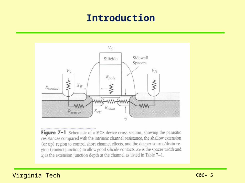
C06- 5Virginia Tech
Introduction
C06- 6Virginia Tech
Introduction
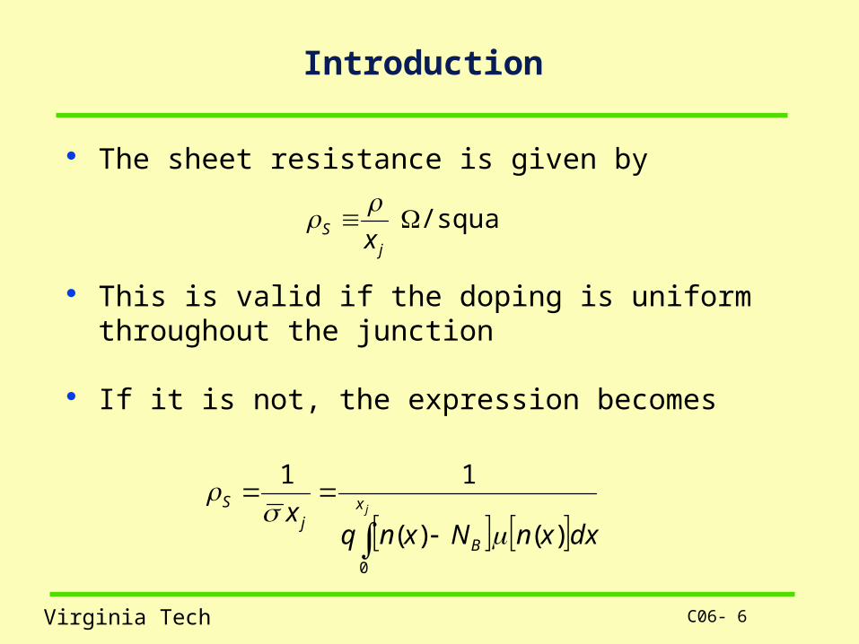
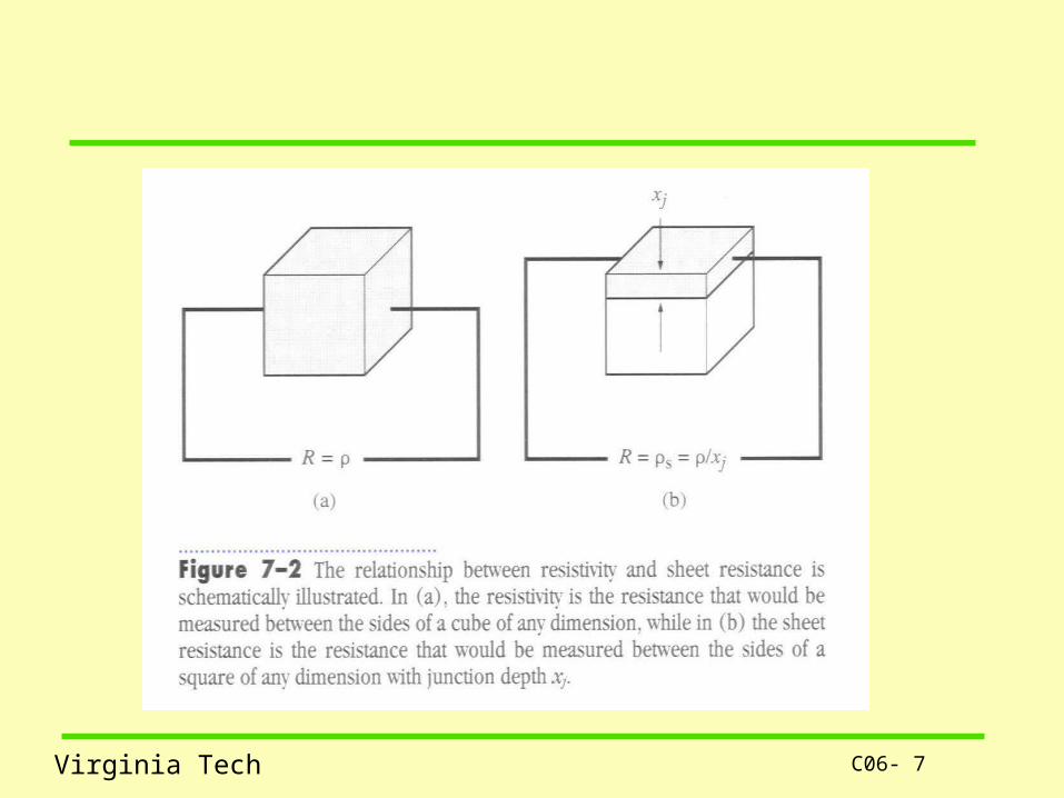
The sheet resistance is given by
This is valid if the doping is uniform throughout the junction
If it is not, the expression becomes
/square j
S x
jx
B
jS
dxxnNxnqx
0
)()(
11
C06- 7Virginia Tech

C06- 8Virginia Tech
Introduction
The challenge is to keep the junctions shallow and yet keep the resistance of the source and drain small to maximize drive current
These are conflicting requirements The NTRS has set goals for shallow junctions
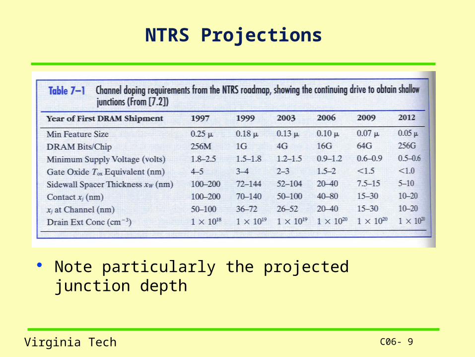
C06- 9Virginia Tech
NTRS Projections
Note particularly the projected junction depth

C06- 10Virginia Tech
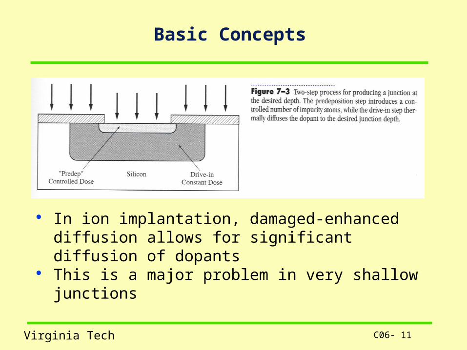
Basic Concepts
Since 1960, the planar process has dominated all methods for creating junctions
The fundamental change in the past 40 years has been how the “predep” has been done.
Predep (predeposition) controls how much impurity is introduced into the wafer
In the 1960s, this was done by solid state diffusion from glass layers or by gas phase diffusion
By the mid-1970s, ion implantation became (and remains) the method of choice
Its only drawback is radiation damage
C06- 11Virginia Tech
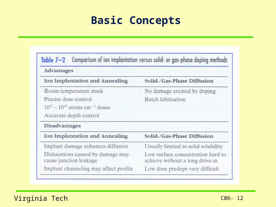
Basic Concepts
In ion implantation, damaged-enhanced diffusion allows for significant diffusion of dopants
This is a major problem in very shallow junctions
C06- 12Virginia Tech
Basic Concepts
C06- 13Virginia Tech
Basic Concepts
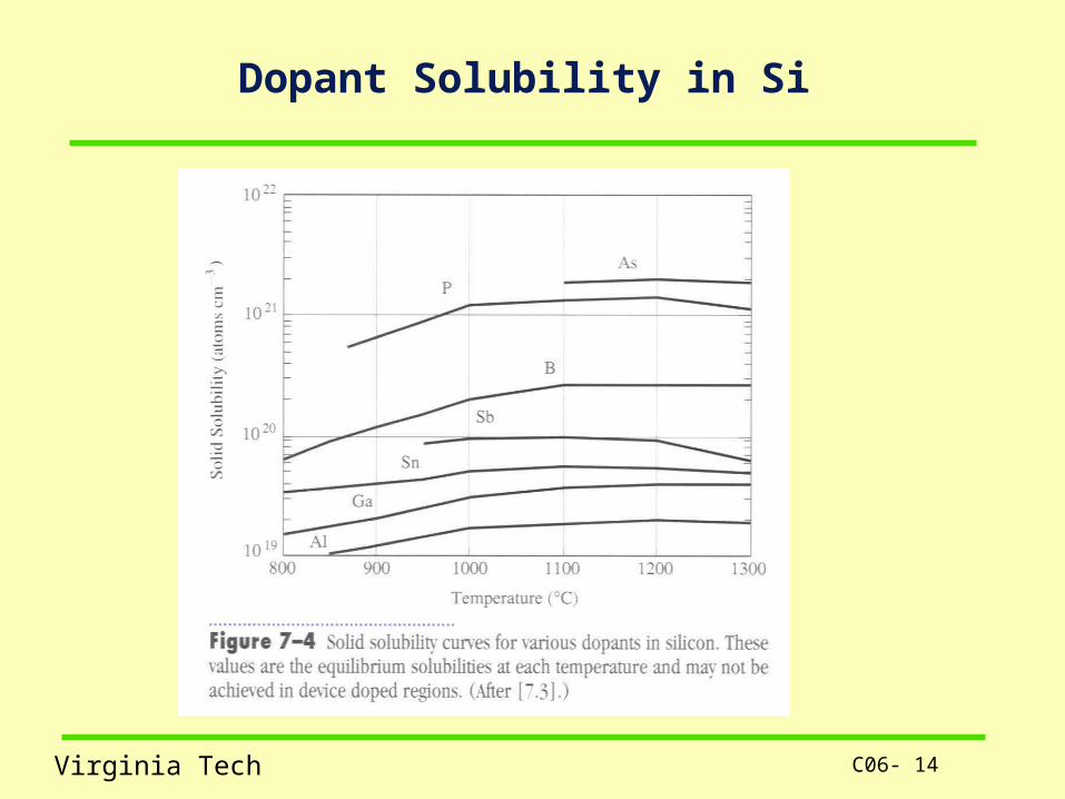
The desired dopants (P, As, B) have only limited solid solubility in Si
The solubility increases with temperature Except, some dopants exhibit retrograde solubility
(where the solubility decreases at elevated temperatures)
If we dope above the solubility limit, precipitates form. When combined in precipitates (or clusters) the dopants do not contribute donors or acceptors (electrons or holes)
The dopant is not electrically active We therefore need to know the maximum amount of
dopant that we can put in Si and maintain electrically active donors and acceptors
C06- 14Virginia Tech
Dopant Solubility in Si

C06- 15Virginia Tech
Solubility Limit
Solubility and electrical activity of impurities in Si
1021
1020
1019
900 1000 1100 1200Temperature ( o C )
Sb
B
P
As
P
As
Solubility limitElectrical active
Impu
rity
con
cent
ratio
n, N
(at
oms/
cm3 )

C06- 16Virginia Tech
Solubility Limit
III-V dopants have limited solubility in Si Surface concentrations can be high. At
1100oC:– B: 3.3 x 1020 cm-3
– P: 1.2 x 1021 cm-3
At high temperatures, impurities cluster without precipitating and have limited electrical activity
3 3As As n
C06- 17Virginia Tech
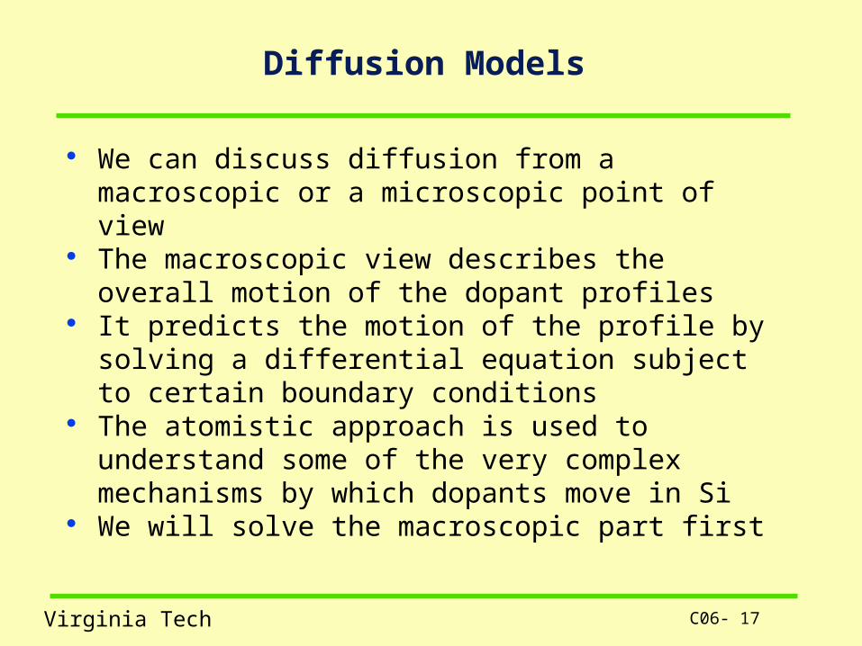
Diffusion Models
We can discuss diffusion from a macroscopic or a microscopic point of view
The macroscopic view describes the overall motion of the dopant profiles
It predicts the motion of the profile by solving a differential equation subject to certain boundary conditions
The atomistic approach is used to understand some of the very complex mechanisms by which dopants move in Si
We will solve the macroscopic part first
C06- 18Virginia Tech
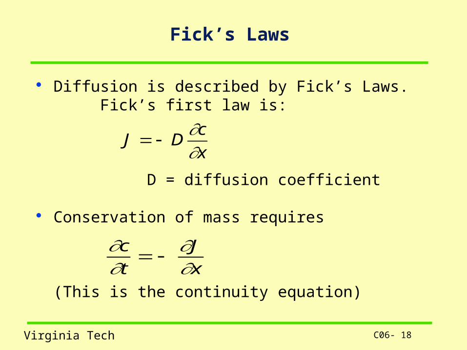
Fick’s Laws
Diffusion is described by Fick’s Laws.Fick’s first law is:
D = diffusion coefficient
Conservation of mass requires
(This is the continuity equation)
J Dc
x
c
t
J
x
C06- 19Virginia Tech
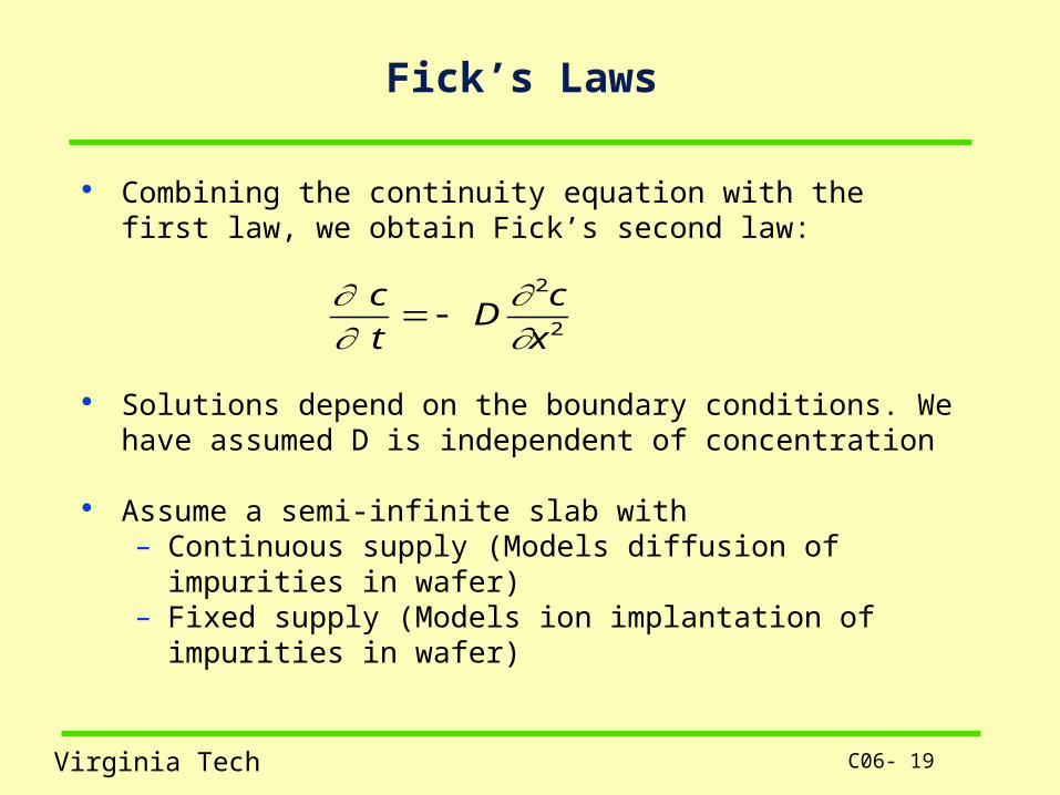
Fick’s Laws
Combining the continuity equation with the first law, we obtain Fick’s second law:
Solutions depend on the boundary conditions. We have assumed D is independent of concentration
Assume a semi-infinite slab with– Continuous supply (Models diffusion of impurities in
wafer)– Fixed supply (Models ion implantation of impurities in
wafer)
c
tD
c
x
2
2
C06- 20Virginia Tech
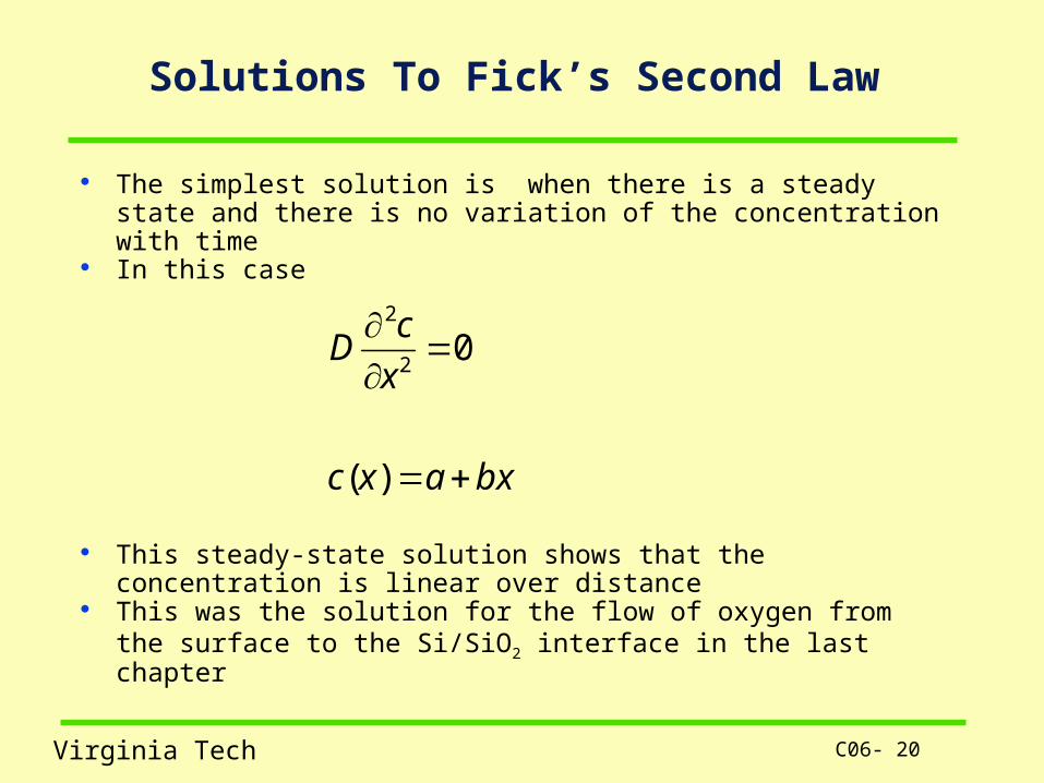
Solutions To Fick’s Second Law
The simplest solution is when there is a steady state and there is no variation of the concentration with time
In this case
This steady-state solution shows that the concentration is linear over distance
This was the solution for the flow of oxygen from the surface to the Si/SiO2 interface in the last chapter
bxaxc
x
cD
)(
02
2

C06- 21Virginia Tech
Solutions To Fick’s Second Law
There are two other solutions of interest The text breaks these into two sub-solutions
each; one for an infinite slab and one for a semi-infinite slab
We will examine only the latter as they approach real conditions
C06- 22Virginia Tech
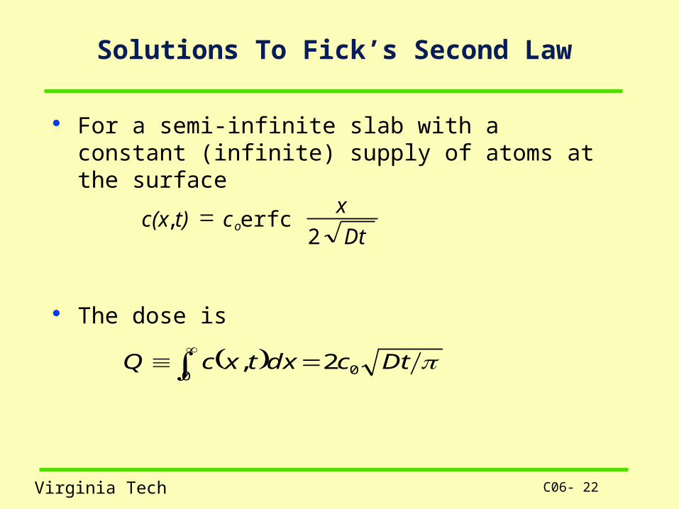
Solutions To Fick’s Second Law
For a semi-infinite slab with a constant (infinite) supply of atoms at the surface
The dose is
0 02, DtcdxtxcQ
c(x t) cx
Dto, erfc
2
C06- 23Virginia Tech
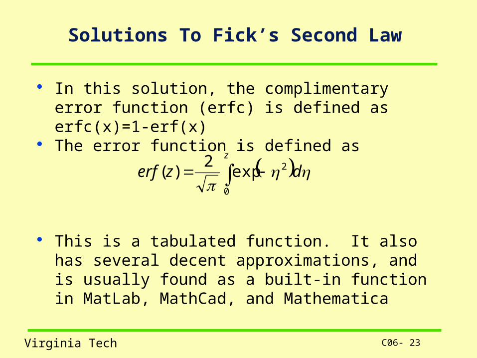
Solutions To Fick’s Second Law
In this solution, the complimentary error function (erfc) is defined as erfc(x)=1-erf(x)
The error function is defined as
This is a tabulated function. It also has several decent approximations, and is usually found as a built-in function in MatLab, MathCad, and Mathematica
z
dzerf0
2exp2
)(
C06- 24Virginia Tech
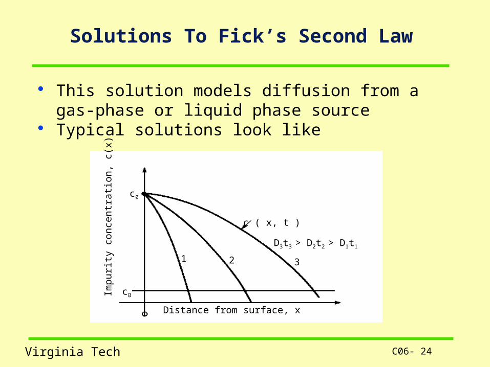
Solutions To Fick’s Second Law
This solution models diffusion from a gas-phase or liquid phase source
Typical solutions look like
c0
cB
Distance from surface, x
1 2 3
D3t3 > D2t2 > D1t1
Impu
rity
con
cent
rati
on, c
(x)
c ( x, t )
C06- 25Virginia Tech
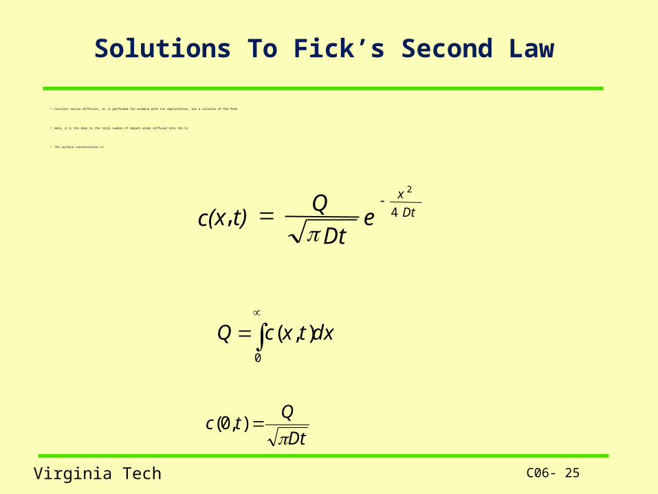
Solutions To Fick’s Second Law
Constant source diffusion, as is performed for example with ion implantation, has a solution of the form
Here, Q is the does or the total number of dopant atoms diffused into the Si
The surface concentration is
dxtxcQ
0
),(
Dt
Qtc
),0(
c(x t)Q
Dte
x
Dt ,
2
4
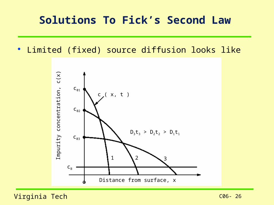
C06- 26Virginia Tech
Solutions To Fick’s Second Law
Limited (fixed) source diffusion looks like
c ( x, t )c01
c02
c03
cB
1 2 3
Distance from surface, x
D3t3 > D2t2 > D1t1
Impu
rity
con
cent
rati
on, c
(x)
C06- 27Virginia Tech
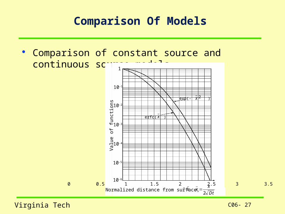
Comparison Of Models
Comparison of constant source and continuous source models
1
10-1
10-2
10-3
10-4
10-5
10-6
0 0.5 1 1.5 2 2.5 3 3.5
Val
ue o
f fu
ncti
ons
Normalized distance from surface, x_
xx
Dt
_
2
exp(- )x_
2
erfc( )x_
C06- 28Virginia Tech
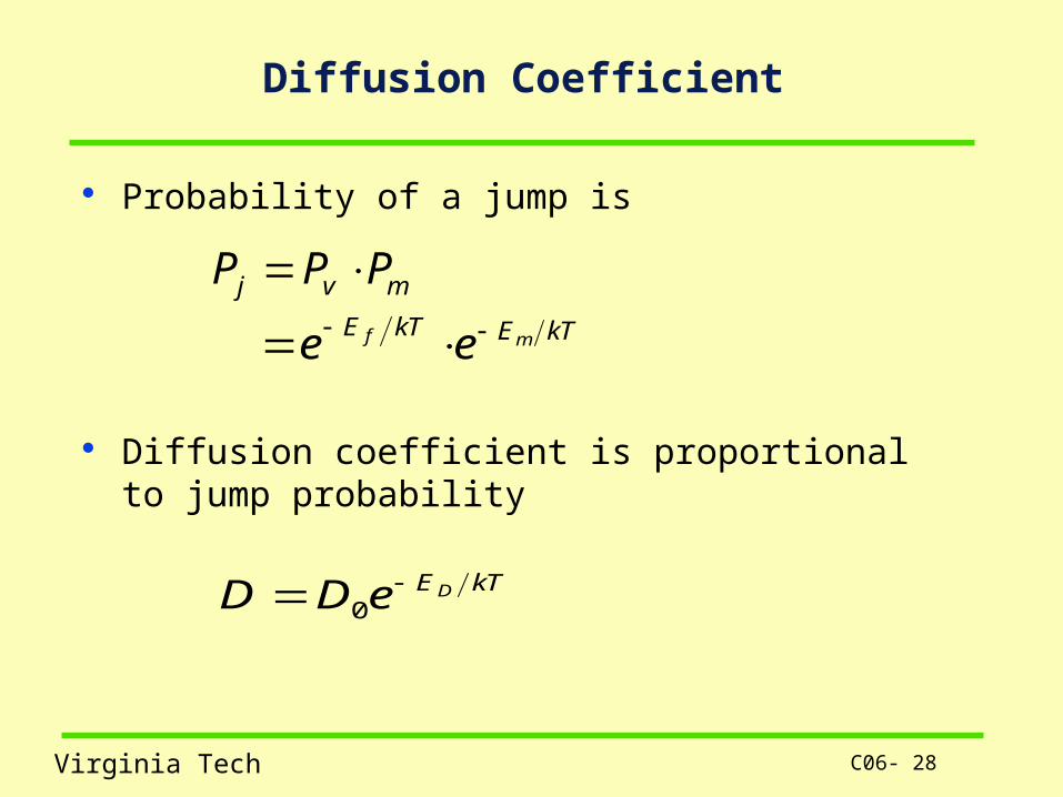
Diffusion Coefficient
Probability of a jump is
Diffusion coefficient is proportional to jump probability
P P Pj v m
e eE kT E kTf m
D D e E kTD 0
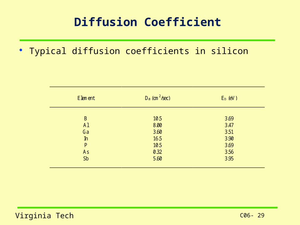
C06- 29Virginia Tech
Diffusion Coefficient
Typical diffusion coefficients in silicon
Element D0 (cm2/sec) ED (eV)
B 10.5 3.69Al 8.00 3.47Ga 3.60 3.51In 16.5 3.90P 10.5 3.69
As 0.32 3.56Sb 5.60 3.95
C06- 30Virginia Tech
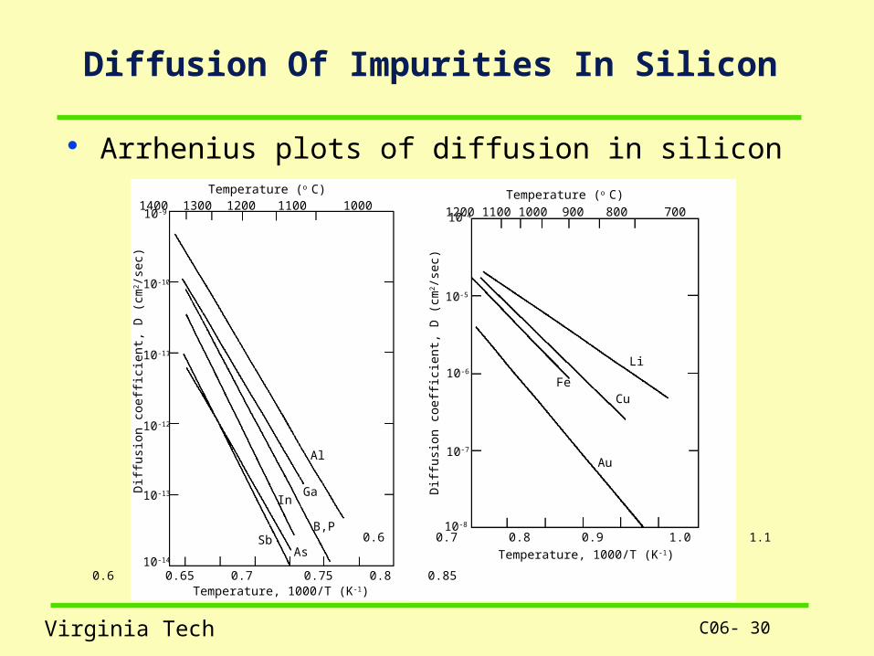
Diffusion Of Impurities In Silicon
Arrhenius plots of diffusion in silicon
1400 1300 1200 1100 1000Temperature (o C)
10-9
10-10
10-11
10-12
10-13
10-14
0.6 0.65 0.7 0.75 0.8 0.85Temperature, 1000/T (K-1)
Al
Ga
B,P
In
AsSb
Dif
fusi
on c
oeff
icie
nt, D
(cm
2 /se
c)
10-4
10-5
10-6
10-7
10-8
0.6 0.7 0.8 0.9 1.0 1.1
Temperature, 1000/T (K-1)
1200 1100 1000 900 800 700
Temperature (o C)
Dif
fusi
on c
oeff
icie
nt, D
(cm
2 /se
c)
Li
CuFe
Au
C06- 31Virginia Tech
Diffusion Of Impurities In Silicon
We recall that the intrinsic carrier concentration in Si is about 7 x 10¹⁸/cc at 1000 C
Thus, if NA and ND are <ni, the material will behave as if it were intrinsic; there are many practical situations where this is a good assumption
The solutions we have given will be valid so long as the concentrations are low enough so that the material is intrinsic at the diffusion temperature
C06- 32Virginia Tech
Diffusion Of Impurities In Silicon
Note that the dopants cluster into “fast” diffusers (P, B, In) and “slow” diffusers (As, Sb)
As we develop shallow devices, slow diffusers are becoming very important
Note that B is the only p-type dopant that has a high solubility; therefore, it is very hard to make shallow p-type junctions with this fast diffuser
We will also find that the theories given here break down as we go to higher concentrations of dopants
C06- 33Virginia Tech
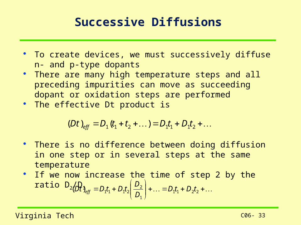
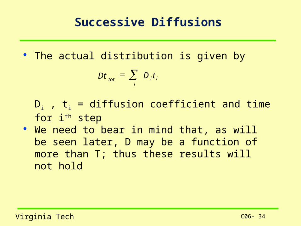
Successive Diffusions
To create devices, we must successively diffuse n- and p-type dopants
There are many high temperature steps and all preceding impurities can move as succeeding dopant or oxidation steps are performed
The effective Dt product is
There is no difference between doing diffusion in one step or in several steps at the same temperature
If we now increase the time of step 2 by the ratio D2/D1
2111211 )()( tDtDttDDt eff
2211
1
22111)( tDtDD
DtDtDDt eff
C06- 34Virginia Tech
Successive Diffusions
The actual distribution is given by
Di , ti = diffusion coefficient and time for ith step
We need to bear in mind that, as will be seen later, D may be a function of more than T; thus these results will not hold
Dt D ttot i i
i

C06- 35Virginia Tech
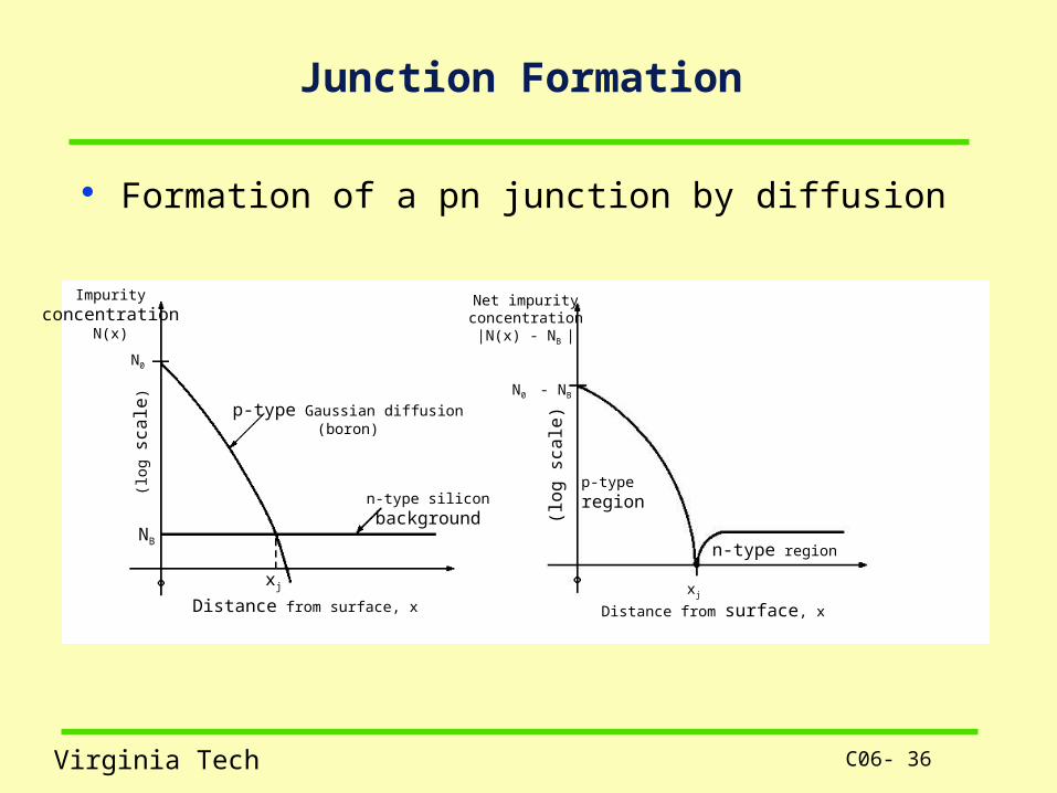
Junction Formation
When diffuse n- and p-type materials, we create a pn junction
When [donor]=[acceptor], the semiconductor material is compensated and we create a metallurgical junction
At metallurgical junction the material behaves intrinsic
We can calculate the position of the metallurgical junction for those systems for which our analytical model is a good fit
C06- 36Virginia Tech
Junction Formation
Formation of a pn junction by diffusion
Impurity
concentrationN(x)
N0
NB
(log
sca
le)
xj
p-type Gaussian diffusion(boron)
n-type silicon
background
Distance from surface, x
Net impurityconcentration
|N(x) - NB |
N0 - NB
p-type
region
n-type region
xj
Distance from surface, x
(log
sca
le)
C06- 37Virginia Tech
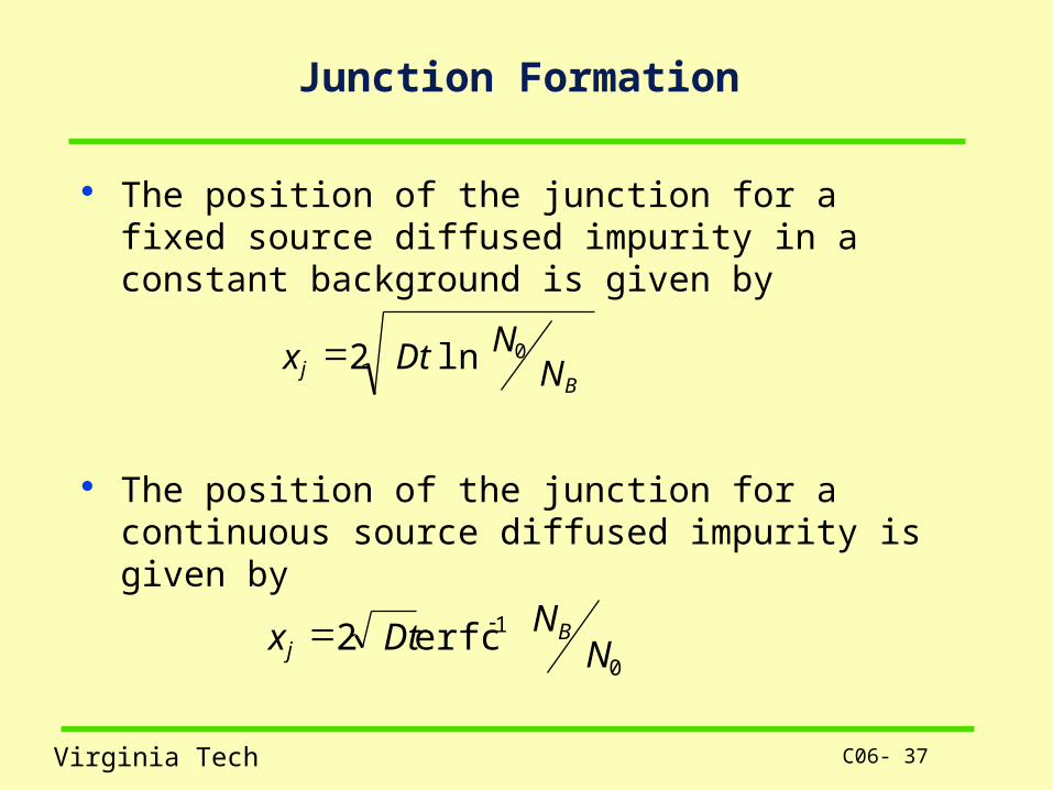
Junction Formation
The position of the junction for a fixed source diffused impurity in a constant background is given by
The position of the junction for a continuous source diffused impurity is given by
x Dt NNjB
2 0ln
x Dt NNj
B 2 1
0erfc
C06- 38Virginia Tech
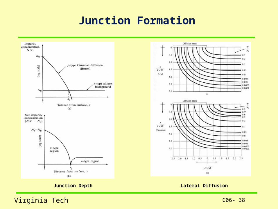
Junction Formation
Junction Depth Lateral Diffusion

C06- 39Virginia Tech
Design and Evaluation
There are three parameters that define a diffused region– The surface concentration– The junction depth– The sheet resistance
These parameters are not independent Irvin developed a relationship that describes
these parameters very well Consider the equation for sheet resistance
jx
B
jS
dxxnNxnqx
0
)()(
11
C06- 40Virginia Tech
Irvin’s Curves
In designing processes, we need to use all available data
We need to determine if one of the analytic solutions applies
For example, – if the surface concentration is near the
solubility limit, perhaps the continuous (erf) solution applies
– If we have a low surface concentration, perhaps the fixed (Gaussian) solution applies
C06- 41Virginia Tech
Irvin’s Curves
If we describe the dopant profile by either the Gaussian or the erf model, we can evaluate the integral
The surface concentration becomes a parameter in this integration
By rearranging the variables, we find that the surface concentration and the product of sheet resistance and the junction depth are related by the definite integral of the profile
There are four separate curves to be evaluated; one pair using either the Gaussian or the erf function, and the other pair for n- or p-type materials (because the mobility is different for electrons and holes)
Typical examples are shown on the following slide
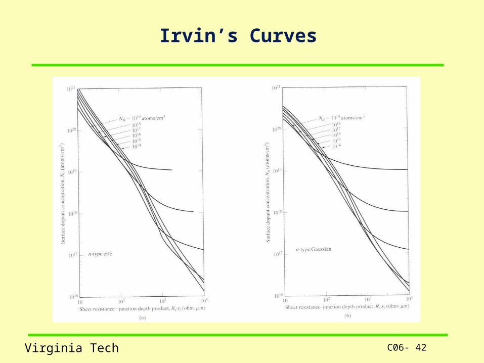
C06- 42Virginia Tech
Irvin’s Curves
C06- 43Virginia Tech
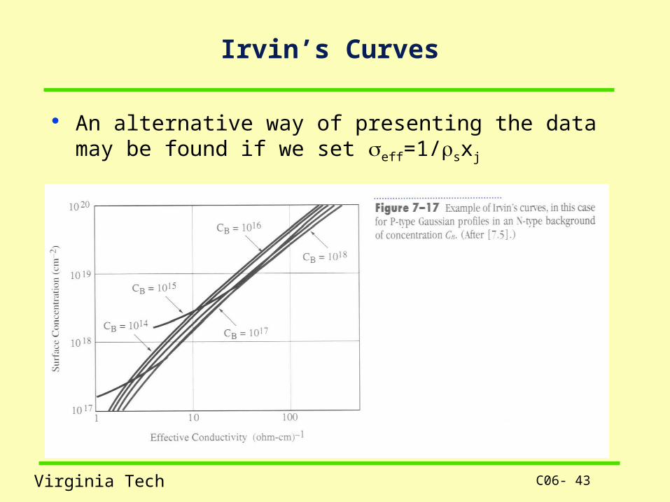
Irvin’s Curves
An alternative way of presenting the data may be found if we set eff=1/sxj
C06- 44Virginia Tech
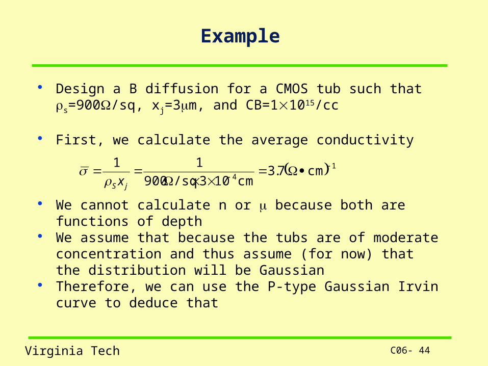
Example
Design a B diffusion for a CMOS tub such that s=900/sq, xj=3m, and CB=11015/cc
First, we calculate the average conductivity
We cannot calculate n or because both are functions of depth
We assume that because the tubs are of moderate concentration and thus assume (for now) that the distribution will be Gaussian
Therefore, we can use the P-type Gaussian Irvin curve to deduce that
1
4cm7.3
cm103/sq900
11
jS x
C06- 45Virginia Tech
Example
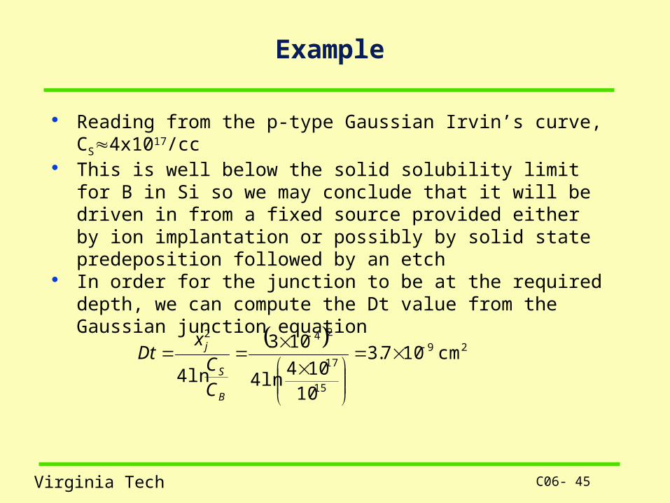
Reading from the p-type Gaussian Irvin’s curve, CS4x1017/cc
This is well below the solid solubility limit for B in Si so we may conclude that it will be driven in from a fixed source provided either by ion implantation or possibly by solid state predeposition followed by an etch
In order for the junction to be at the required depth, we can compute the Dt value from the Gaussian junction equation
29
15
17
242
cm 107.3
10104
ln4
103
ln4
B
S
j
CC
xDt
C06- 46Virginia Tech
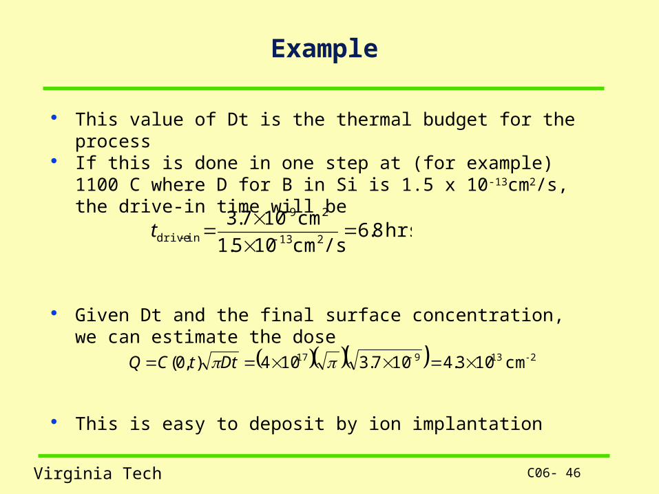
Example
This value of Dt is the thermal budget for the process If this is done in one step at (for example) 1100 C
where D for B in Si is 1.5 x 10⁻¹³cm2/s, the drive-in time will be
Given Dt and the final surface concentration, we can estimate the dose
This is easy to deposit by ion implantation
hrs 8.6/scm105.1
cm107.3213
29
indrive
t
213917 cm 103.4107.3104),0( -DttCQ
C06- 47Virginia Tech
Example
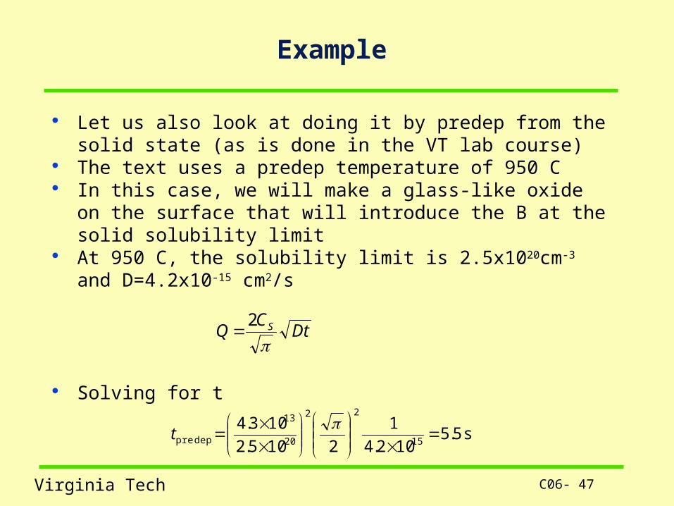
Let us also look at doing it by predep from the solid state (as is done in the VT lab course)
The text uses a predep temperature of 950 C In this case, we will make a glass-like oxide on the
surface that will introduce the B at the solid solubility limit
At 950 C, the solubility limit is 2.5x1020cm-3 and D=4.2x10⁻¹⁵ cm2/s
Solving for t
DtC
Q S
2
s 5.5102.4
1
2105.2
103.415
22
20
13
deppre
t
C06- 48Virginia Tech
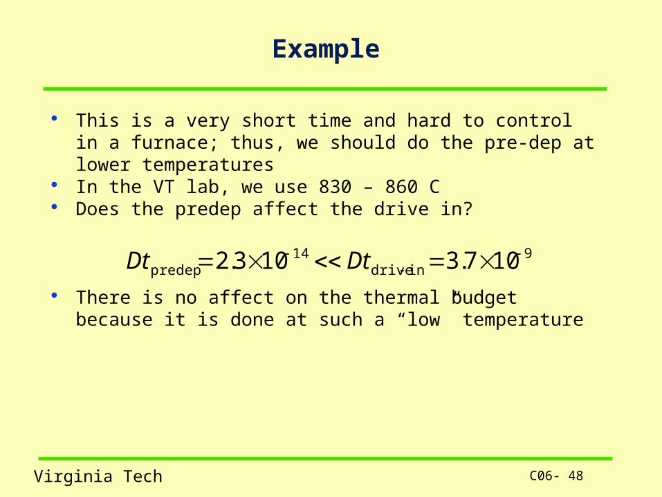
Example
This is a very short time and hard to control in a furnace; thus, we should do the pre-dep at lower temperatures
In the VT lab, we use 830 – 860 C Does the predep affect the drive in?
There is no affect on the thermal budget because it is done at such a “low” temperature
9indrive
14predep 107.3103.2
DtDt
C06- 49Virginia Tech
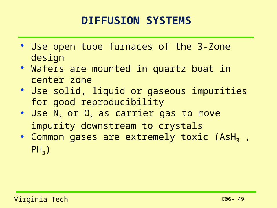
DIFFUSION SYSTEMS
Use open tube furnaces of the 3-Zone design Wafers are mounted in quartz boat in center
zone Use solid, liquid or gaseous impurities for good
reproducibility Use N2 or O2 as carrier gas to move impurity
downstream to crystals Common gases are extremely toxic (AsH3 ,
PH3)
C06- 50Virginia Tech
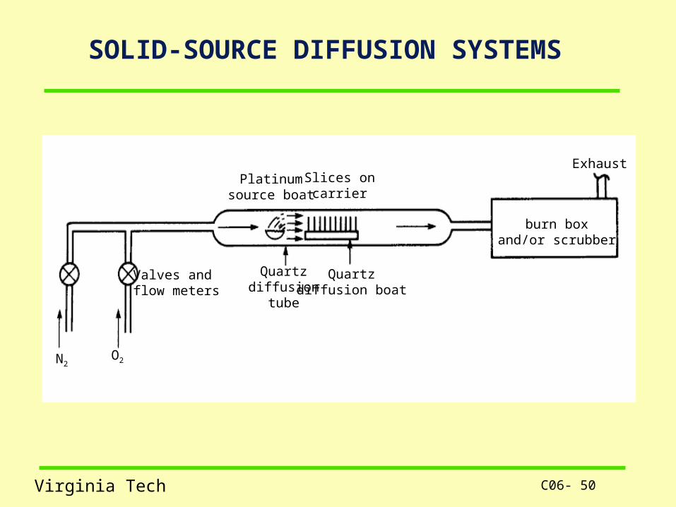
SOLID-SOURCE DIFFUSION SYSTEMS
N2O2
Valves andflow meters
Platinumsource boat
Slices oncarrier
Quartzdiffusion
tube
Quartzdiffusion boat
burn boxand/or scrubber
Exhaust
C06- 51Virginia Tech
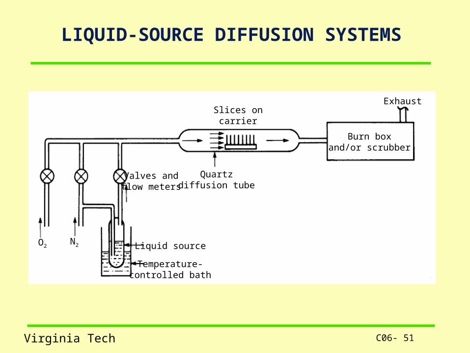
LIQUID-SOURCE DIFFUSION SYSTEMS
Burn boxand/or scrubber
ExhaustSlices on
carrier
Quartzdiffusion tube
Valves andflow meters
Liquid source
Temperature-controlled bath
N2O2
C06- 52Virginia Tech
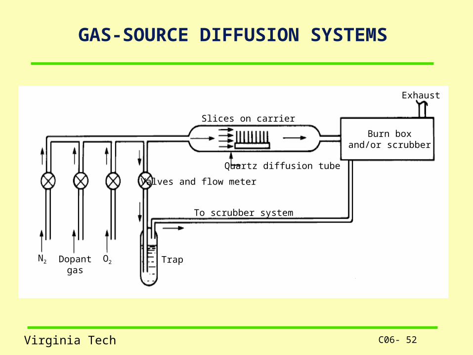
GAS-SOURCE DIFFUSION SYSTEMS
Burn boxand/or scrubber
Exhaust
N2 Dopantgas
O2
Valves and flow meter
To scrubber system
Trap
Slices on carrier
Quartz diffusion tube
C06- 53Virginia Tech
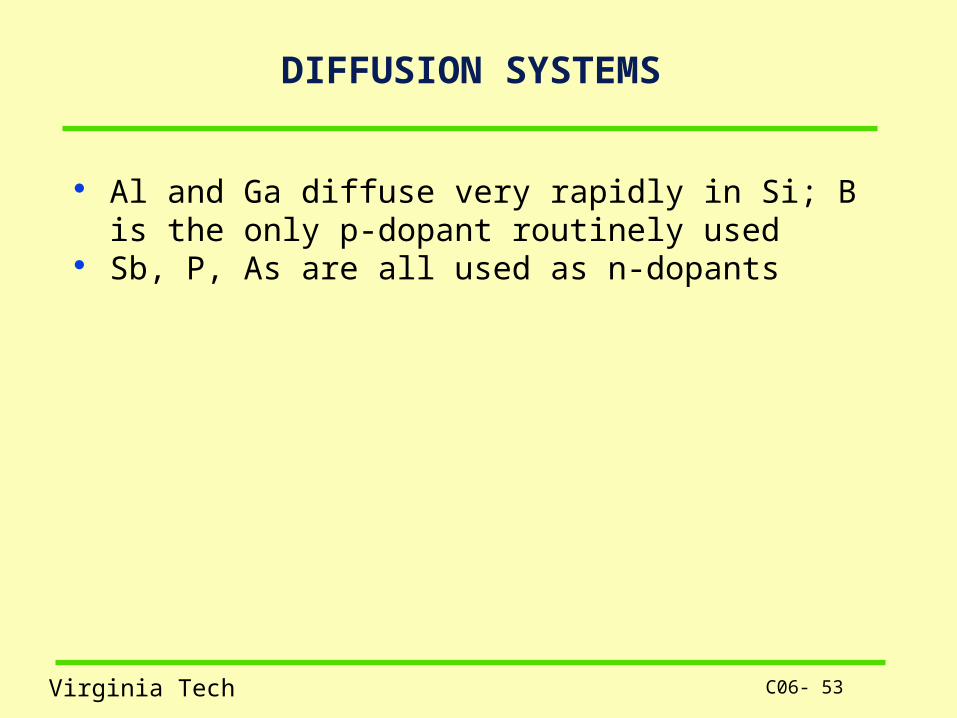
DIFFUSION SYSTEMS
Al and Ga diffuse very rapidly in Si; B is the only p-dopant routinely used
Sb, P, As are all used as n-dopants

C06- 54Virginia Tech
DIFFUSION SYSTEMS
Typical reactions for solid impurities are:
2 9 6 9
2 4
4 30 2 6
2 5 4
2 3 3 4
2 3 3 4
3 3 2900
2 3 2 2
2 3 2
3 2 2 5 2
2 5 2
2 3 2
2 3 2
CHO B O BO CO HO
BO Si SiO B
POCl PO Cl
PO Si SiO P
AsO Si SiO As
SbO Si SiO Sb
oC

C06- 55Virginia Tech
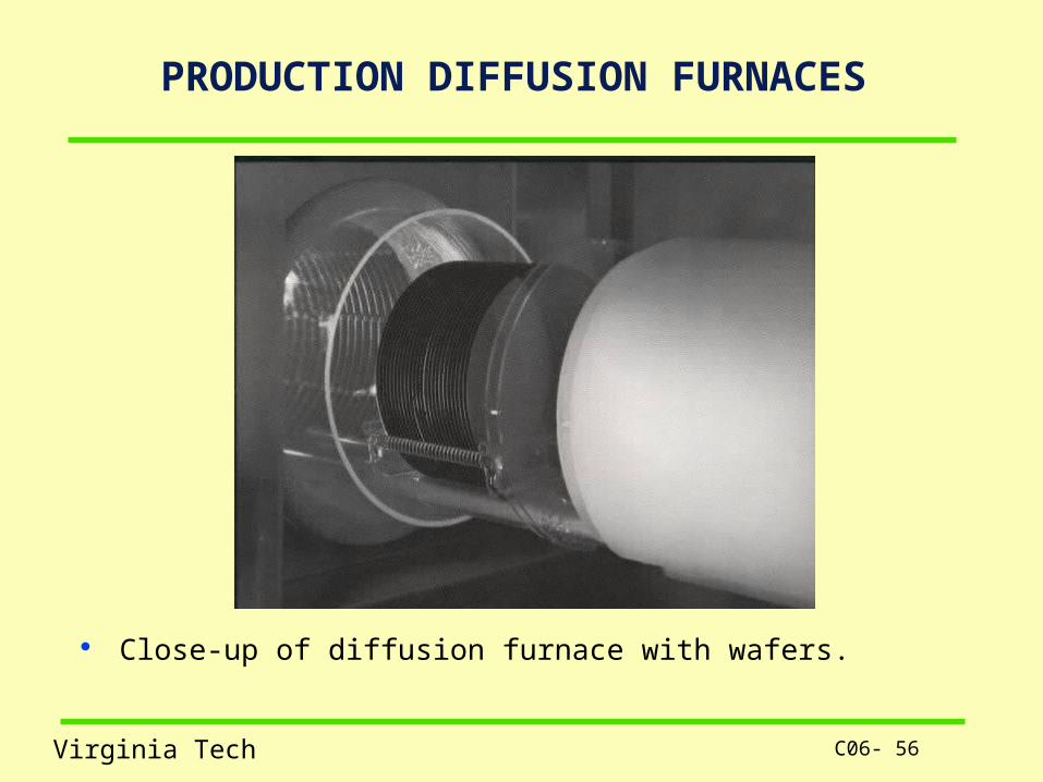
PRODUCTION DIFFUSION FURNACES
Commercial diffusion furnace showing the furnace with wafers (left) and gas control system (right). (Photo courtesy of Tystar Corp.)
C06- 56Virginia Tech
PRODUCTION DIFFUSION FURNACES
Close-up of diffusion furnace with wafers.
C06- 57Virginia Tech
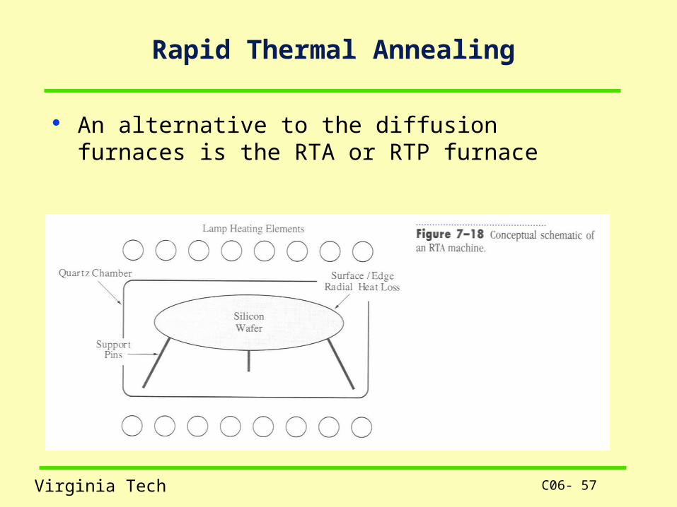
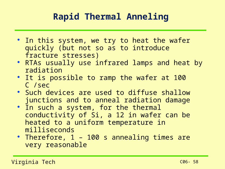
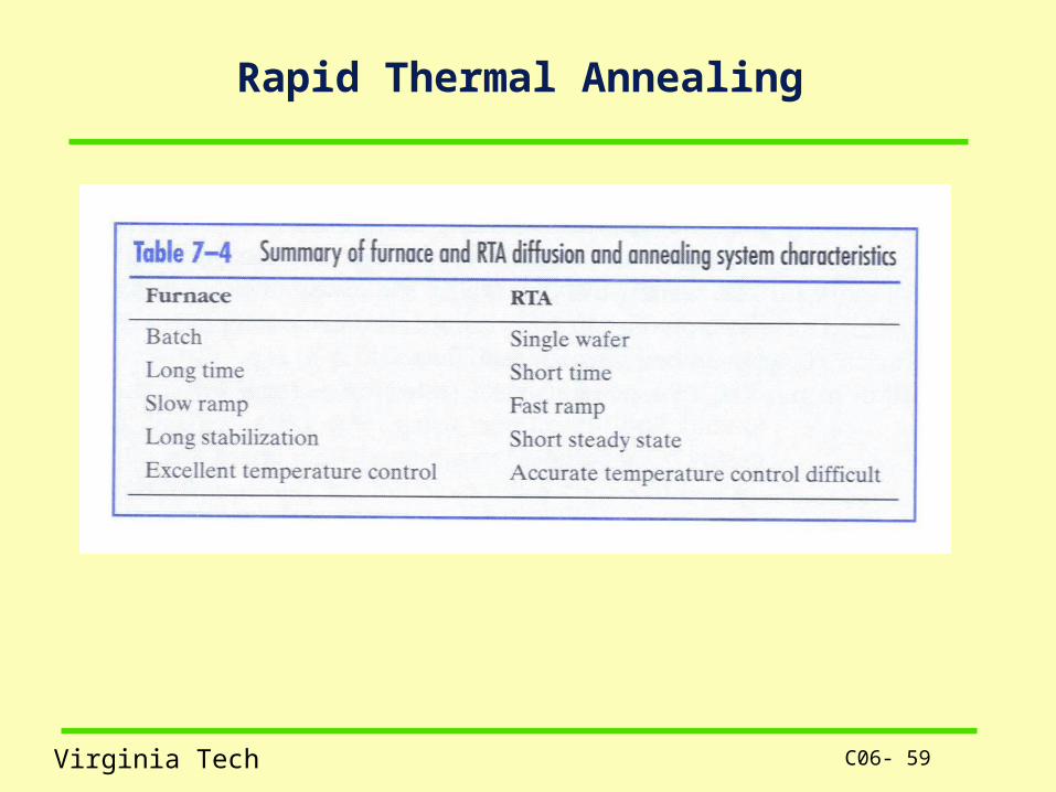
Rapid Thermal Annealing
An alternative to the diffusion furnaces is the RTA or RTP furnace
C06- 58Virginia Tech
Rapid Thermal Anneling
In this system, we try to heat the wafer quickly (but not so as to introduce fracture stresses)
RTAs usually use infrared lamps and heat by radiation
It is possible to ramp the wafer at 100 C /sec Such devices are used to diffuse shallow
junctions and to anneal radiation damage In such a system, for the thermal conductivity
of Si, a 12 in wafer can be heated to a uniform temperature in milliseconds
Therefore, 1 – 100 s annealing times are very reasonable
C06- 59Virginia Tech
Rapid Thermal Annealing
C06- 60Virginia Tech
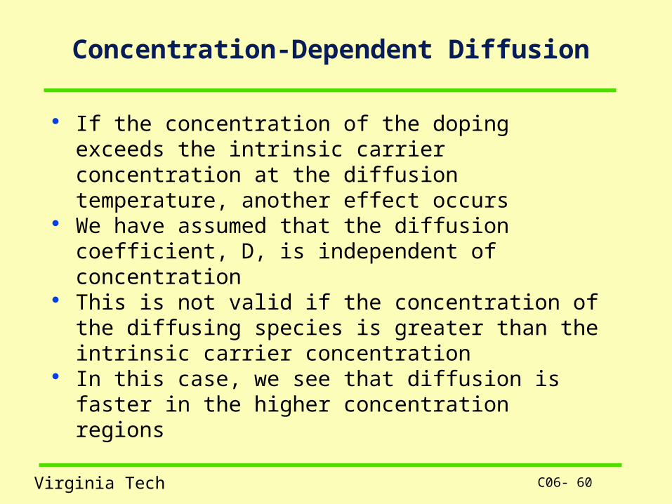
Concentration-Dependent Diffusion
If the concentration of the doping exceeds the intrinsic carrier concentration at the diffusion temperature, another effect occurs
We have assumed that the diffusion coefficient, D, is independent of concentration
This is not valid if the concentration of the diffusing species is greater than the intrinsic carrier concentration
In this case, we see that diffusion is faster in the higher concentration regions
C06- 61Virginia Tech
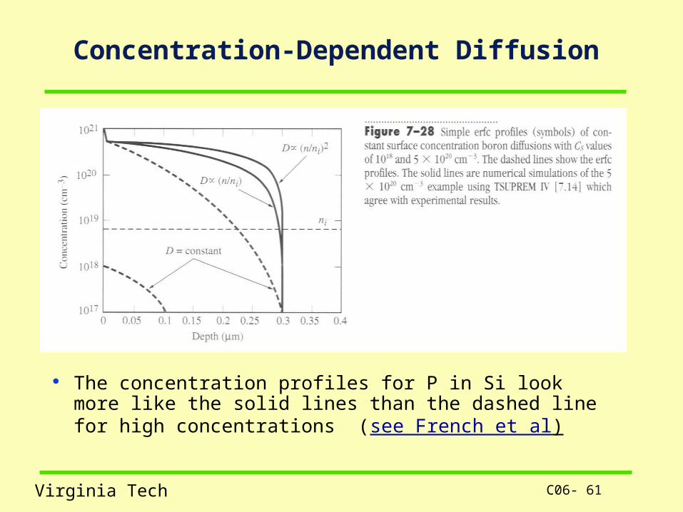
Concentration-Dependent Diffusion
The concentration profiles for P in Si look more like the solid lines than the dashed line for high concentrations (see French et al)
C06- 62Virginia Tech
Concentration-Dependent Diffusion
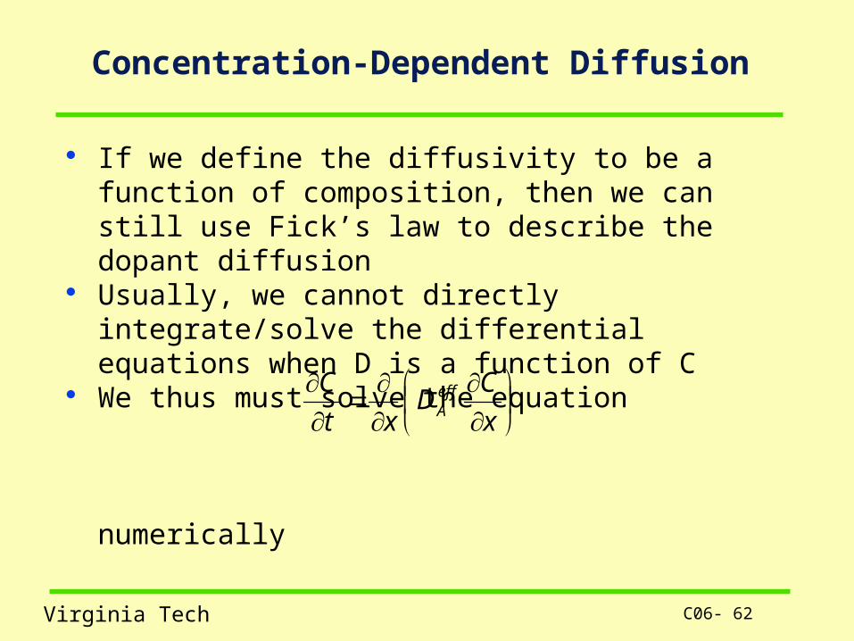
If we define the diffusivity to be a function of composition, then we can still use Fick’s law to describe the dopant diffusion
Usually, we cannot directly integrate/solve the differential equations when D is a function of C
We thus must solve the equation
numerically
x
CD
xt
C effA
C06- 63Virginia Tech
Concentration-Dependent Diffusion
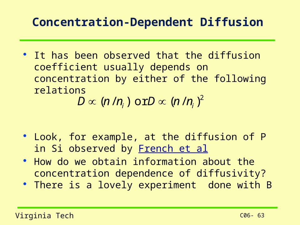
It has been observed that the diffusion coefficient usually depends on concentration by either of the following relations
Look, for example, at the diffusion of P in Si observed by French et al
How do we obtain information about the concentration dependence of diffusivity?
There is a lovely experiment done with B
2)/(or )/( ii nnDnnD
C06- 64Virginia Tech
Concentration-Dependent Diffusion
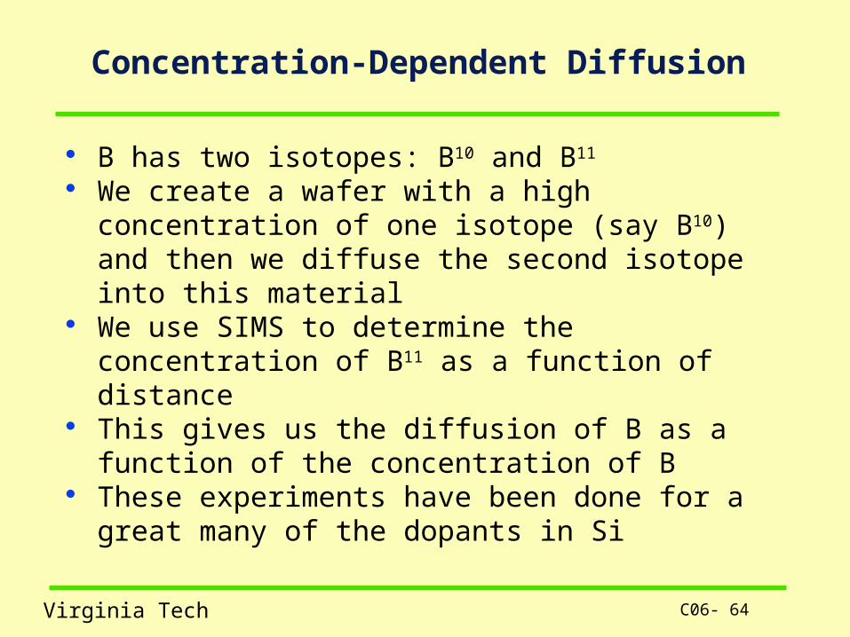
B has two isotopes: B10 and B11
We create a wafer with a high concentration of one isotope (say B10) and then we diffuse the second isotope into this material
We use SIMS to determine the concentration of B11 as a function of distance
This gives us the diffusion of B as a function of the concentration of B
These experiments have been done for a great many of the dopants in Si
C06- 65Virginia Tech
Concentration-Dependent Diffusion
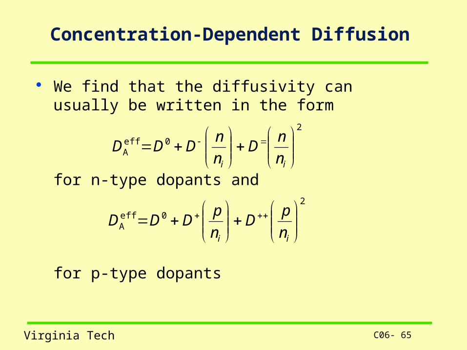
We find that the diffusivity can usually be written in the form
for n-type dopants and
for p-type dopants
2
0effA
ii n
nD
n
nDDD
2
0effA
ii n
pD
n
pDDD
C06- 66Virginia Tech
Concentration-Dependent Diffusion
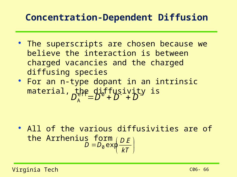
The superscripts are chosen because we believe the interaction is between charged vacancies and the charged diffusing species
For an n-type dopant in an intrinsic material, the diffusivity is
All of the various diffusivities are of the Arrhenius form
DDDD 0effA
kT
EDDD
.exp0
C06- 67Virginia Tech
Concentration-Dependent Diffusion
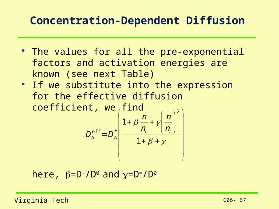
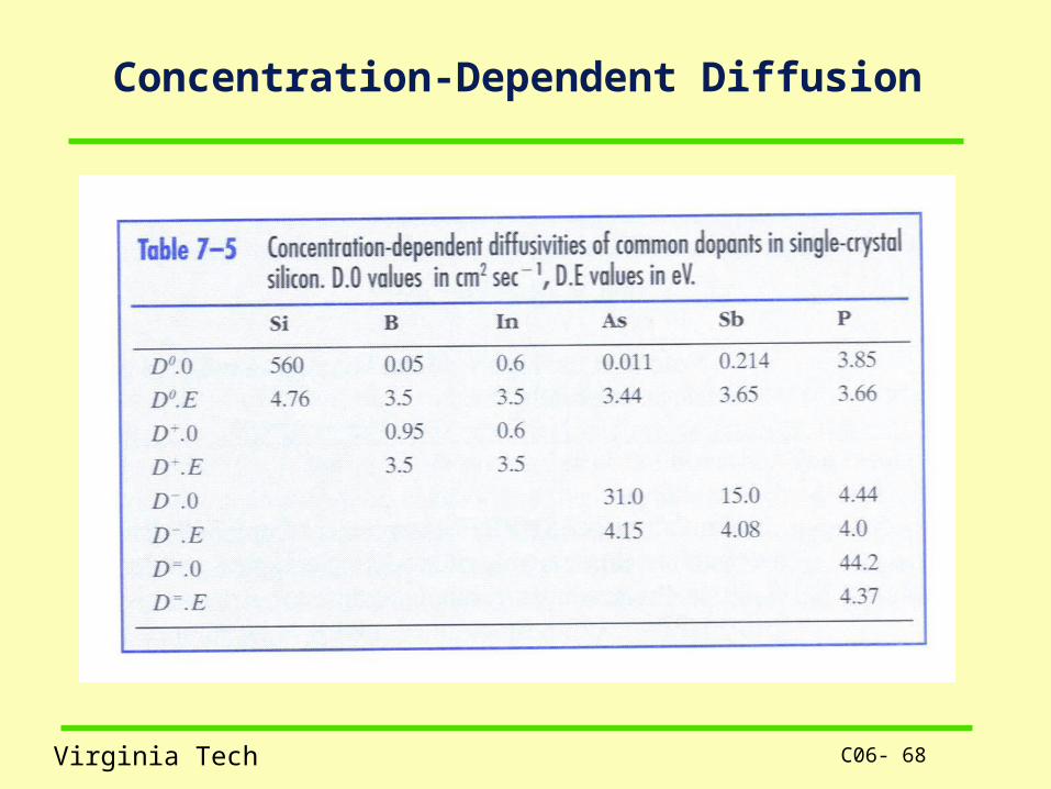
The values for all the pre-exponential factors and activation energies are known (see next Table)
If we substitute into the expression for the effective diffusion coefficient, we find
here, =D-/D0 and =D=/D0
1
12
*effA
iiA
nn
nn
DD
C06- 68Virginia Tech
Concentration-Dependent Diffusion
C06- 69Virginia Tech
Concentration-Dependent Diffusion
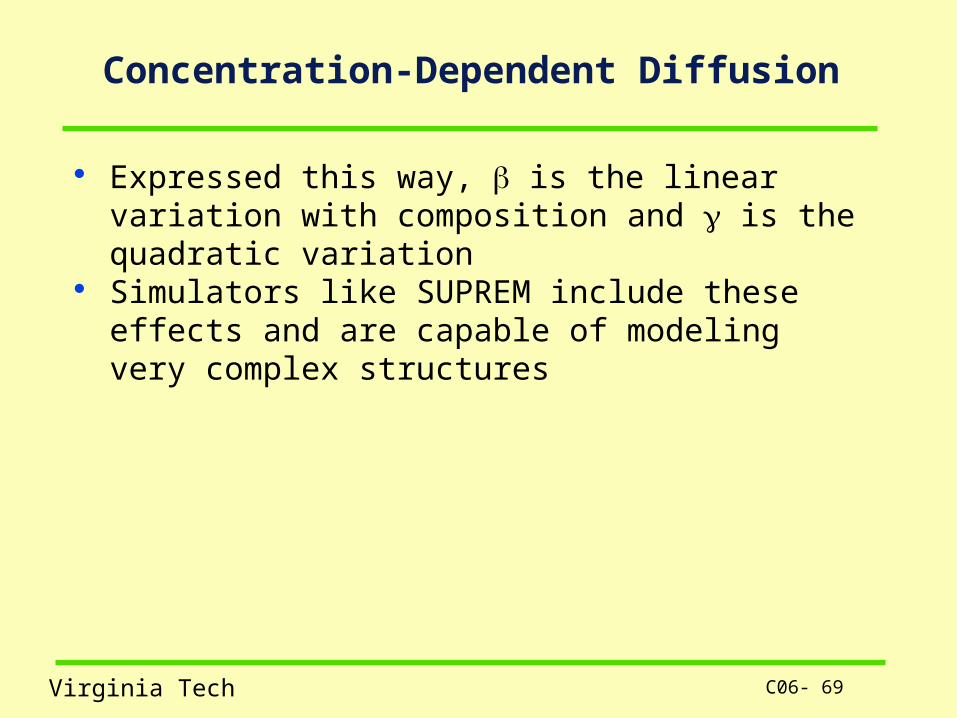
Expressed this way, is the linear variation with composition and is the quadratic variation
Simulators like SUPREM include these effects and are capable of modeling very complex structures


![Dopant Diffusion – physics [Repaired]](https://static.fdocuments.in/doc/165x107/577d20d41a28ab4e1e93db83/dopant-diffusion-physics-repaired.jpg)