by Scott Rixner Rice University
134
Stream Processor Architecture by Scott Rixner Rice University
Transcript of by Scott Rixner Rice University

Stream Processor Architecture
by
Scott RixnerRice University

ii Stream Processor Architecture


iv Stream Processor Architecture

Contents
Foreword............................................................................. ix
Acknowledgements...........................................................xiii
1 Introduction................................................................... 1
1.1 Stream Architecture........................................................................................21.1.1 Stream Programming .........................................................................................21.1.2 Bandwidth Hierarchy .........................................................................................41.1.3 Parallel Processing ............................................................................................6
1.2 The Imagine Media Processor........................................................................7
1.3 Contributions..................................................................................................9
1.4 Overview ........................................................................................................9
2 Background.................................................................. 11
2.1 Special-purpose Media Processors...............................................................11
2.2 Programmable Media Processors .................................................................12
2.3 Vector Processors .........................................................................................13
v
STREAM PROCESSOR ARCHITECTURE
2.4 Stream Processors ........................................................................................13
2.5 Storage Hierarchy.........................................................................................14
2.6 DRAM Access Scheduling...........................................................................15
2.7 Summary ......................................................................................................16
3 Media Processing Applications .................................. 19
3.1 Media Processing .........................................................................................19
3.2 Sample Applications ....................................................................................203.2.1 Stereo Depth Extraction ...................................................................................203.2.2 MPEG2 Encoding ............................................................................................203.2.3 QR Matrix Decomposition ...............................................................................213.2.4 Space-time Adaptive Processing ......................................................................213.2.5 Polygon Rendering...........................................................................................21
3.3 Application Characteristics ..........................................................................223.3.1 Operations........................................................................................................223.3.2 Global Data......................................................................................................233.3.3 Compute Intensity.............................................................................................243.3.4 Summary...........................................................................................................24
4 The Imagine Stream Processor .................................. 27
4.1 Stream Processing ........................................................................................284.1.1 Stream Programming .......................................................................................294.1.2 MPEG2 I-frame Encoding ...............................................................................30
4.2 Architecture..................................................................................................344.2.1 Stream Register File (SRF) ..............................................................................354.2.2 Arithmetic Clusters...........................................................................................374.2.3 Microcontroller ................................................................................................394.2.4 Streaming Memory System ...............................................................................404.2.5 Network Interface.............................................................................................424.2.6 Stream Controller .............................................................................................434.2.7 Host Processor .................................................................................................43
4.3 Programming Model ....................................................................................444.3.1 Stream-level Programming ..............................................................................444.3.2 Kernel-level Programming...............................................................................47
4.4 Implementation.............................................................................................48
vi

CONTENTS
4.5 Scalability and Extensibility.........................................................................504.5.1 Scalability.........................................................................................................504.5.2 Extensibility......................................................................................................51
5 Data Bandwidth Hierarchy ........................................ 53
5.1 Overview ......................................................................................................53
5.2 Communication Bottlenecks ........................................................................565.2.1 Register File Structure .....................................................................................585.2.2 Cache Hierarchy ..............................................................................................585.2.3 DRAM...............................................................................................................59
5.3 Register Organization...................................................................................60
5.4 Evaluation.....................................................................................................645.4.1 Kernel Comparison ..........................................................................................655.4.2 Application Evaluation.....................................................................................725.4.3 Application Bandwidth Demands.....................................................................755.4.4 Bandwidth Sensitivity .......................................................................................785.4.5 Arithmetic Unit Utilization...............................................................................79
5.5 Summary ......................................................................................................82
6 Memory Access Scheduling........................................ 83
6.1 Overview ......................................................................................................846.1.1 Stream Memory Transfers ................................................................................846.1.2 Memory Access Scheduling..............................................................................86
6.2 Modern DRAM ............................................................................................88
6.3 Memory Access Scheduling.........................................................................926.3.1 Architecture ......................................................................................................926.3.2 Algorithms ........................................................................................................94
6.4 Evaluation.....................................................................................................966.4.1 Microbenchmarks.............................................................................................966.4.2 Memory Demands ..........................................................................................1006.4.3 Application Performance ...............................................................................101
6.5 Summary ....................................................................................................105
vii

STREAM PROCESSOR ARCHITECTURE
7 Conclusions ................................................................ 107
7.1 Imagine Summary ......................................................................................108
7.2 Future Architectures ...................................................................................109
References ........................................................................ 113
Index................................................................................. 119
viii

Foreword
We stand at the brink of a revolution in computer architecture. The conventional (vonNeumann) processor architecture that has reigned for over 50 years is likely to bereplaced over the next decade. This pending revolution is driven by two factors: thewire-limited nature of emerging semiconductor technology and the trend towardmedia applications. Professor Rixner, in this monograph, shows how architecture canevolve to match emerging technology to demanding media applications.
Advancing semiconductor technology enables us to pack an enormous amount ofarithmetic capability on a single chip but also limits the communication latency andbandwidth both on and off chip. As wire widths shrink the delay of wires dominatesthe delay of transistors and gates. These trends place a premium on locality – to mini-mize communication – and concurrency – to make use of the large numbers of arith-metic units. Conventional processors can exploit neither locality nor concurrency.They have a single arithmetic unit and lump all storage at a given level (e.g., registers,cache, main memory) together — rather than localizing storage near its point of use.
Media applications also change the equation. Compared to conventional applications– for which processors have been tuned over decades – they have little spatial or tem-poral locality – a pixel of an image is often visited exactly once – and hence arepoorly matched to conventional cache-based memory systems. They make use oflow-precision fixed-point data types (16-bits is typical) as opposed to the high-preci-sion (64-bit) data of scientific applications. They also have enormous amounts of dataparallelism – all pixels can be processed in parallel – so they can tolerate considerablelatency.
ix

STREAM PROCESSOR ARCHITECTURE
In this monograph, Professor Rixner shows how a stream processor architecture isideally suited for applying emerging, wire-limited semiconductor technology tomedia applications. Stream processors operate by passing streams of data recordsthrough computation kernels. Operating on streams allows the concurrency of moderntechnology to be applied to the data parallelism of media applications. Explicitlydividing the application into kernels exposes locality on two levels. At one level, datawithin each kernel is entirely local to the kernel and can be kept entirely in local reg-isters. At the next level, a stream generated by one kernel and consumed in the nextcan be passed through stream register file so it consumes no memory bandwidth —even if each pixel is only touched once. Stream processing shares its ability to exploitconcurrency with vector processing. It is distinguished from vector processing in itsability to exploit locality.
Professor Rixner explores stream processing in the context of the Imagine stream pro-cessor which was developed in my research group at MIT and Stanford from 1996 to2001. As described in Chapter 4 of this monograph, Imagine is a load-store architec-ture for streams. All operations pass streams into and out of a stream register file(SRF) that serves as a nexus for the processor. Load and store operations pass streamsof records – not words or vectors – between memory and the SRF. Network opera-tions send and receive streams of records. Finally, arithmetic kernels operate on oneor more streams from the SRF generating new streams that are in turn written to theSRF. Professor Rixner explains this stream architecture in detail and shows how itefficiently supports the abstraction of stream programming.
After reviewing stream architecture and the Imagine stream processor, Professor Rix-ner addresses two aspects of optimizing bandwidth in stream processors: the use of abandwidth hierarchy and the optimization of DRAM accesses. In Chapter 5, ProfessorRixner shows how organizing storage into three levels – local registers, stream regis-ters, and memory – can supply a large number of function units with data. The band-width hierarchy results in most data movement occurring where bandwidth isinexpensive – between local registers and adjacent ALUs. With order of magnitudereductions in bandwidth moving out to the stream registers and to memory respec-tively. This organization enables a relatively modest 2GB/s memory system in Imag-ine to support an ALU complex that can demand over 500GB/s of local bandwidth.
Memory access scheduling reorders memory operations to maximize the bandwidthrealized from a conventional DRAM. Modern dynamic random access memories arein fact not random access. Their bandwidth and latency depends strongly on theaccess pattern. In Chapter 6, Professor Rixner shows that reordering memory opera-tions to match the internal structure of the DRAMs can result in significant bandwidthimprovement.
x

FOREWARD
Stream processing is in its infancy, but it promises to be a major force in the comingdecade. As the Imagine project moves toward completion and a working prototypethe next steps in the evolution of stream processing are already taking shape. MajorCPU vendors are evaluating the use of stream processors as media co-processors forconventional CPUs. Stream processing is being considered for a new generation ofsupercomputing. Also, researchers are looking at ways to generalize stream process-ing to make it applicable to a wider range of applications.
In this monograph, Professor Rixner gives the reader an accessible introduction to theemerging field of stream processing along with a scientific exploration of key band-width issues affecting the architecture of stream processing. Readers wanting to jointhe upcoming revolution in computer architecture are encouraged to read on.
William J. DallyStanford UniversityPalo Alto, CaliforniaAugust 1, 2001
xi

STREAM PROCESSOR ARCHITECTURE
xii

Acknowledgements
A victorious army first wins and then seeks battle; a defeated army first battles andthen seeks victory.
-Sun Tzu, The Art of War
I would like to thank Professor William J. Dally, to whom I am greatly indebted. Hehas an amazing ability to only fight the battles worth fighting which shows in thequality of his research program. I can only hope that some of that ability has rubbedoff on me. Bill has provided me with countless opportunities to lead and to learn that Idoubt I would have found otherwise. I am thankful to Bill for giving me the opportu-nity to take a leadership role on the Imagine project, which while not always easy,was a tremendous experience. Bill also gave me the opportunity to spend severalyears at Stanford University, and while I may not have embraced Stanford, the time Ispent there was invaluable. Thanks also to the members of my thesis committee atMIT, Professors Leonard McMillan and Donald Troxel.
The Imagine project is the work of many, and this research would not have been pos-sible without the contributions of others. I would like to thank the Imagine team:Ujval Kapasi, Brucek Khailany, Peter Mattson, John Owens, and many others whocontributed along the way. We are all grateful to each other for pulling together tomake such an ambitious project successful.
xiii

STREAM PROCESSOR ARCHITECTURE
Many thanks go to my officemates Steve Keckler and Kelly Shaw. They not only putup with me all of those years, but also made my days as a graduate student enjoyable.I only hope I did the same for them.
I would also like to thank those who helped with the preparation of this document.Shelley Russell typed early versions of many chapters and proofread the final docu-ment. Without her help, my wrists may not have lasted to allow me to finish writing.Kelly Shaw spent countless hours proofreading all of the chapters at least once. Hercomments significantly improved the overall quality of the writing.
My family has supported me throughout the process. There were many struggles andmany accomplishments along the way, but through them all, they were always there.Thanks.
The research described here was supported by the Defense Advanced ResearchProjects Agency under ARPA order E254 and monitored by the Army IntelligenceCenter under contract DABT63-96-C-0037.
xiv

CHAPTER 1 Introduction
Media processing applications, such as three-dimensional graphics, video compres-sion, and image processing, demand very high arithmetic rates. To meet the demandsof these applications, a programmable media processor must support tens to hundredsof arithmetic units. In modern VLSI, hundreds of arithmetic units can easily fit on amodestly sized 1cm2 chip. The challenge, however, is to efficiently provide the neces-sary data bandwidth to keep those units busy. A stream architecture, which includes adata bandwidth hierarchy, enables a programmable media processor implemented inmodern VLSI technology to efficiently provide data bandwidth for tens to hundredsof arithmetic units.
Applications must make efficient use of the available bandwidth in order to achievehigh sustained computation rates. Media processing applications can naturally beexpressed as a sequence of computation kernels that operate on data streams. Thesestream programs map easily and efficiently to the data bandwidth hierarchy of thestream architecture. This enables media processing applications to utilize inexpensivelocal data bandwidth when possible, and consume expensive global data bandwidthonly when necessary.
The Imagine media processor implements a stream architecture to provide high sus-tained media processing performance. Imagine supports 48 arithmetic units with athree-tiered data bandwidth hierarchy, yielding a peak computation rate of 20 billionfloating-point operations per second (GFLOPS). Applications are able to sustain asignificant fraction of this peak rate. For example, QR matrix decomposition, useful
Introduction 1
Introduction
in many signal processing applications, can be performed on Imagine at a sustainedrate of 12.5GFLOPS.
1.1 Stream Architecture
The stream programming model exposes the locality and concurrency in media pro-cessing applications. In this model, applications are expressed as a sequence of com-putation kernels that operate on streams of data. A kernel is a small program that isrepeated for each successive element in its input streams to produce output streamsthat are fed to subsequent kernels. Each data stream is a variable length collection ofrecords, where each record is a logical grouping of media data. For example, a recordcould represent a triangle vertex in a polygon rendering application or a pixel in animage processing application. A data stream would then be a sequence of hundreds ofthese vertices or pixels. In the stream programming model, locality and concurrencyare exposed both within a kernel and between kernels.
1.1.1 Stream Programming
To illustrate the stream programming model, consider the stream program for theintracoded frame (I-frame) encoder of an MPEG2 encoder. An MPEG2 encoder takesa video sequence as input and compresses the sequence of images into a single bitstream consisting of the following three types of frames: intracoded (I), predicted (P),and bidirectional (B). I-frames are compressed using only information contained inthe current frame. P- and B-frames are compressed using information from the cur-rent frame and additional reference frames. This example application will be dis-cussed further in subsequent chapters.
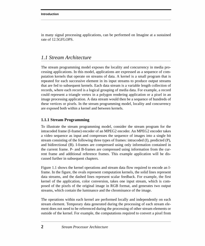
Figure 1.1 shows the kernel operations and stream data flow required to encode an I-frame. In the figure, the ovals represent computation kernels, the solid lines representdata streams, and the dashed lines represent scalar feedback. For example, the firstkernel of the application, color conversion, takes one input stream, which is com-posed of the pixels of the original image in RGB format, and generates two outputstreams, which contain the luminance and the chrominance of the image.
The operations within each kernel are performed locally and independently on eachstream element. Temporary data generated during the processing of each stream ele-ment does not need to be referenced during the processing of other stream elements oroutside of the kernel. For example, the computations required to convert a pixel from
2 Stream Processor Architecture
Stream Architecture
RGB format to luminance and chrominance generate numerous temporary values.These temporaries do not affect other pixels and will never be referenced again afterthe pixel is converted. Therefore, that data is local to the kernel while it is processingeach pixel in its input stream. Also, since the processing of each stream element islargely independent of the processing of other stream elements, multiple elements canbe processed concurrently by the kernels. For instance, given enough hardware, thecolor conversion kernel could convert every pixel in the input image simultaneously,as the calculations for each pixel do not depend on the calculations for any otherpixel.
As can be seen in the figure, kernels communicate between each other by passing datastreams from one kernel to the next. The color conversion kernel, for example passesa stream of luminance values to the Discrete Cosine Transform (DCT) kernel. Theselocalized stream transfers replace arbitrary global data references, yielding simple,regular communication patterns among kernels. Since kernels only pass data streamsfrom one kernel to the next, multiple kernels can also operate concurrently on succes-sive data streams in a pipelined fashion. One processor could convert the stream ofRGB pixels into luminance and chrominance values in batches of several hundredpixels, while another processor could simultaneously transform previously convertedbatches of pixels into the frequency domain using the DCT.
FIGURE 1.1 I-Frame Encoding from MPEG2 Encoder
ColorConversion
DCT
DCT IDCT
IDCT
Run-LevelEncoding
VariableLengthCoding
Input ImageLuminance
ChrominanceLuminance Reference
Chrominance Reference
Bitstream
Rate Control
Kernels
Streams
ScalarFeedback
Introduction 3
Introduction
1.1.2 Bandwidth Hierarchy
A stream architecture can exploit the locality inherent in media processing applica-tions when they are expressed in the stream programming model. A stream architec-ture is organized around a three-tiered bandwidth hierarchy that includes a streamingmemory system, a global stream register file, and local register files that feed thearithmetic units.
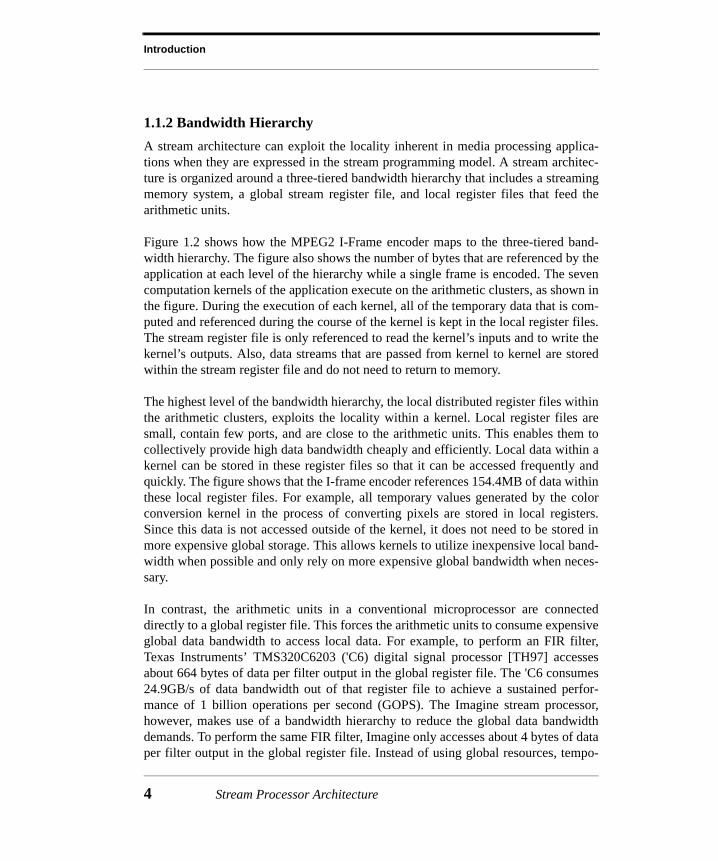
Figure 1.2 shows how the MPEG2 I-Frame encoder maps to the three-tiered band-width hierarchy. The figure also shows the number of bytes that are referenced by theapplication at each level of the hierarchy while a single frame is encoded. The sevencomputation kernels of the application execute on the arithmetic clusters, as shown inthe figure. During the execution of each kernel, all of the temporary data that is com-puted and referenced during the course of the kernel is kept in the local register files.The stream register file is only referenced to read the kernel’s inputs and to write thekernel’s outputs. Also, data streams that are passed from kernel to kernel are storedwithin the stream register file and do not need to return to memory.
The highest level of the bandwidth hierarchy, the local distributed register files withinthe arithmetic clusters, exploits the locality within a kernel. Local register files aresmall, contain few ports, and are close to the arithmetic units. This enables them tocollectively provide high data bandwidth cheaply and efficiently. Local data within akernel can be stored in these register files so that it can be accessed frequently andquickly. The figure shows that the I-frame encoder references 154.4MB of data withinthese local register files. For example, all temporary values generated by the colorconversion kernel in the process of converting pixels are stored in local registers.Since this data is not accessed outside of the kernel, it does not need to be stored inmore expensive global storage. This allows kernels to utilize inexpensive local band-width when possible and only rely on more expensive global bandwidth when neces-sary.
In contrast, the arithmetic units in a conventional microprocessor are connecteddirectly to a global register file. This forces the arithmetic units to consume expensiveglobal data bandwidth to access local data. For example, to perform an FIR filter,Texas Instruments’ TMS320C6203 ('C6) digital signal processor [TH97] accessesabout 664 bytes of data per filter output in the global register file. The 'C6 consumes24.9GB/s of data bandwidth out of that register file to achieve a sustained perfor-mance of 1 billion operations per second (GOPS). The Imagine stream processor,however, makes use of a bandwidth hierarchy to reduce the global data bandwidthdemands. To perform the same FIR filter, Imagine only accesses about 4 bytes of dataper filter output in the global register file. Instead of using global resources, tempo-
4 Stream Processor Architecture
Stream Architecture
rary data is stored and accessed in local register files. The consumption of global databandwidth is drastically reduced to 2.6GB/s. By using over 273GB/s of inexpensivelocal data bandwidth, Imagine is able to achieve a performance of over 17GOPS.
The center of the bandwidth hierarchy, the stream register file, exploits the localitybetween kernels. The stream register file is a large global register file that allows datato be accessed sequentially as streams by the arithmetic clusters and the memory sys-tem. Kernels consume their input streams from the stream register file and store their
FIGURE 1.2 I-Frame Encoding from MPEG2 Encoder
ColorConversion
DCT
DCT
IDCT
IDCT
Run-LevelEncoding
VariableLengthCoding
Arithmetic ClustersStream Register FileMemory (or I/O)
InputImage
RGBPixels
LuminancePixels
TransformedLuminance
LuminanceReference
EncodedBitstream
RLE Stream
Bitstream
ReferenceChrominance
Image
ReferenceLuminance
Image
ChrominancePixels
TransformedChrominance
ChrominanceReference
Data Referenced: 835KB 4.8MB 154.4MB
MemoryBandwidth
SRFBandwidth
Introduction 5
Introduction
produced output streams back to the stream register file. These output streams thenbecome the input streams of subsequent kernels, enabling the stream register file toexploit the locality of stream recirculation. When a kernel finishes processing itsstreams, its outputs remain in the stream register file to be used as inputs for anotherkernel. For example, the luminance values that are generated by the color conversionkernel are stored in the stream register file until they can be processed by the DCTkernel; they never return to memory. The figure shows that the I-frame encoder refer-ences 4.8MB of data within the stream register file. This is 32 times fewer referencesthan are made to the local register files. Storing intermediate streams in the globalstream register file eliminates costly memory references, allowing stream programs toutilize global bandwidth when possible and rely on more expensive memory band-width only when necessary.
The lowest level of the bandwidth hierarchy, the streaming memory system, is uti-lized for global data storage. In the I-frame encoder, no intermediate data generated inthe encoding process of the current frame is stored to memory. The only memory ref-erences that the application performs are to read the original, unencoded image, towrite the final encoded bit stream, and to write the reference images that will be usedto encode future P- or B-frames, resulting in 835KB of memory references. About sixtimes less data is referenced in memory than in the stream register file and about 189times less data is referenced in memory than in the local register files for this applica-tion.
1.1.3 Parallel Processing
A stream architecture can also exploit the concurrency inherent in media processingapplications when they are expressed in the stream programming model. The band-width hierarchy scales the data bandwidth across multiple levels to support largenumbers of arithmetic units. These arithmetic units are organized into single-instruc-tion, multiple-data (SIMD) clusters that perform identical computations on differentdata elements. Each cluster contains multiple arithmetic units that are controlled by avery long instruction word (VLIW). The arithmetic clusters store temporary datalocally, but transfer global data into and out of the stream register file. To enable mul-tiple stream processors to be interconnected, the stream register file also connects to anetwork interface. The network interface allows entire data streams to be transferredfrom the stream register file of one processor to the stream register file of another pro-cessor through an external network.
The SIMD arithmetic clusters exploit the concurrency within kernels by operating onmultiple stream elements simultaneously. A single, shared controller issues the same
6 Stream Processor Architecture
The Imagine Media Processor
instructions to each cluster as they each operate on different elements of the kernel’sinput data streams. An arithmetic cluster contains multiple arithmetic units thatexploit the instruction-level parallelism within the kernels. By using software pipelin-ing, each cluster can also process multiple stream elements simultaneously. The com-bination of data parallelism, instruction-level parallelism, and software pipeliningallows a stream processor to utilize large numbers of arithmetic units for media pro-cessing applications.
Multiple processors can exploit the concurrency among kernels by executing severalkernels simultaneously. By splitting up the kernels in an application across the proces-sors, multiple kernels can operate in parallel on different sections of the data. The firstprocessor in the pipeline would execute one or more kernels to produce outputstreams that would then be passed to the next processor. As the next processor oper-ates on those streams, the original processor could repeat its kernels on the next set ofinput data. Depending on the amount of parallelism in the program, this pipelinecould be arbitrarily wide, in terms of the number of processors executing the samekernels across the data, or deep, in terms of the number of processors in the pipeline.
1.2 The Imagine Media Processor
Imagine is designed to be a proof-of-concept programmable stream processor show-ing the viability of structures such as the bandwidth hierarchy to enable scalablemicroprocessors that deliver high sustained multimedia performance. Imagine isorganized around a three-tiered data bandwidth hierarchy consisting of a streamingmemory system (2GB/s), a global stream register file (32GB/s), and a set of local dis-tributed register files located near the arithmetic units (544GB/s). The bandwidthhierarchy of Imagine therefore provides memory bandwidth, global register band-width, and local register bandwidth with a ratio of 1:16:272. For each word accessedin memory, 16 words may be accessed in the global stream register file, and 272words may be accessed in the clusters’ local register file. At the lowest level, thememory system is designed to maximize the bandwidth of stream data transfers fromexternal DRAM, rather than minimize the latency of individual references. The128KB SRF at the center of the bandwidth hierarchy not only provides intermediatestorage for data streams but also enables additional stream clients to be modularlyconnected to Imagine, such as a streaming network interface or a graphics texturecaching unit. At the highest level, local, distributed register files feed 48 arithmeticunits organized into a SIMD array of eight identical clusters.
Introduction 7

Introduction
Figure 1.3 shows a block diagram of Imagine’s microarchitecture. Imagine isdesigned to be a coprocessor that operates on multimedia data streams. The streamregister file (SRF) effectively isolates the arithmetic units from the memory system,making Imagine a load/store architecture for streams. As shown in the figure, eightarithmetic clusters, a microcontroller, a streaming memory system, a network inter-face, and a stream controller are connected to the SRF. The arithmetic clusters con-sume data streams from the SRF, process them, and return their output data streams tothe SRF. The eight clusters operate simultaneously on interleaved data records trans-ferred from the SRF, allowing eight elements to be processed in parallel. Each arith-metic cluster contains three adders, two multipliers, and one divide/square root unit.These units are controlled by statically scheduled VLIW instructions issued by themicrocontroller.
Imagine is targeted to operate at 500MHz in a 0.15µm CMOS standard-cell imple-mentation. The peak computation rate of the 48 arithmetic units is 20GOPS for both32-bit integer and floating-point operations. For 16-bit and 8-bit parallel-subwordoperations, the peak performance increases to 40 and 80GOPS, respectively.
FIGURE 1.3 Imagine Block Diagram
Imagine Stream Processor
Stream Register FileNetworkInterface
StreamController
Streaming Memory System
AL
U C
lust
er 0
AL
U C
lust
er 7
AL
U C
lust
er 6
AL
U C
lust
er 5
AL
U C
lust
er 4
AL
U C
lust
er 3
AL
U C
lust
er 2
AL
U C
lust
er 1
Mic
roco
ntro
ller
SDRAM SDRAMSDRAM SDRAM
Net
wor
kHostProcessor
8 Stream Processor Architecture

Contributions
1.3 Contributions
The primary contributions of this research are as follows:
1. The concept of a bandwidth hierarchy which efficiently utilizes data bandwidthfor media processing applications at three levels: local register files, global regis-ter files, and off-chip memory.
2. The architecture of a memory access scheduler to maximize the sustainablethroughput of modern DRAM.
3. The architecture of a bandwidth-efficient stream processor that can sustain a sig-nificant fraction of its peak performance on media processing applications.
4. An experimental evaluation of the data bandwidth demands of media processingapplications, the effectiveness of the bandwidth hierarchy, and the benefits ofmemory access scheduling.
1.4 Overview
This work focuses on the efficient use of data bandwidth for media processing appli-cations. Chapter 2 presents background information on media processors and band-width management. The chapter shows that media processors have mirrored thedesigns of more conventional programmable processors with slight deviations. Thestorage hierarchy of a conventional processor, however, is not able to provide suffi-cient data bandwidth for media processing, as it is designed to minimize latency,rather than maximize bandwidth.
Chapter 3 presents the differentiating characteristics of media processing applica-tions. These applications operate on streams of low-precision integer data, have abun-dant data parallelism, do not reuse global data frequently, and perform tens tohundreds of computations per global data reference. These characteristics differ fromthose of traditional applications for which modern programmable processors havebeen designed, motivating a departure from conventional microarchitectures formedia processing.
Chapter 4 presents the architecture of the Imagine stream processor. Imagine is orga-nized around a three-tiered bandwidth hierarchy that effectively supports 48 arith-metic units for media processing applications. Imagine is designed to demonstratethat an efficient bandwidth hierarchy enables high sustained multimedia performance.Imagine is expected to fit on a chip about 2.5cm2 in size and deliver a peak perfor-
Introduction 9

Introduction
mance of 20GFLOPS. Media processing applications can actually achieve and sustainfrom a quarter to over half of the peak computation rate.
Chapter 5 introduces the concept of a data bandwidth hierarchy that efficiently pro-vides data bandwidth to the arithmetic units of a media processor. The chapter showshow technology constraints and media processing characteristics motivate microar-chitectures for media processing that include storage hierarchies that scale the pro-vided data bandwidth across multiple levels. A data bandwidth hierarchy enables amedia processor to effectively utilize tens to hundreds of arithmetic units to sustainhigh computation rates.
Chapter 6 introduces the concept of memory access scheduling to maximize the sus-tained bandwidth of external DRAM at the lowest level of the data bandwidth hierar-chy. The structure of modern DRAMs makes their achievable throughput and latencyhighly dependent on the access pattern. Memory access scheduling takes advantage ofthe internal structure of DRAM to reorder DRAM operations to maximize sustainedthroughput.
Finally, Chapter 7 reiterates the importance of careful bandwidth management tomaximize media processing performance subject to the constraints of modern VLSItechnology.
10 Stream Processor Architecture
CHAPTER 2 Background
In order to provide the peak computation rates that media applications demand, mod-ern media processors typically take advantage of special-purpose hardware. Theseprocessors sacrifice the flexibility of programmability but provide high multimediaperformance by efficiently utilizing silicon resources. Special-purpose solutions man-age bandwidth efficiently for the particular application they target. Programmableprocessors, in contrast, must rely on more flexible structures to support a wider rangeof applications. The data parallelism inherent to media processing applicationsenables the use of efficient SIMD and vector operations, but programmable proces-sors still must be able to communicate data among arithmetic units and memory in aflexible manner. Therefore, these processors have traditionally included cache or reg-ister hierarchies. To be effective for media processing, these hierarchies require highsustained bandwidth from external memory. However, the techniques used to maxi-mize bandwidth largely neglect the scatter/gather access patterns commonly found incomplicated media processing applications, such as MPEG encoding and three-dimensional graphics.
2.1 Special-purpose Media Processors
Media processing systems typically employ dedicated, special-purpose hardware tomeet the performance demands of media applications, especially three-dimensionalgraphics. For example, the InfiniteReality from SGI is a special-purpose multiproces-
Background 11

Background
sor system designed to provide high sustained graphics performance [MBDM97]. TheInfiniteReality is composed of four custom Geometry Engines and 80-320 customImage Engines. Combined, these special-purpose processors are able to delivergraphics rendering performance of up to 11 million triangles per second and 830 mil-lion pixels per second. Overall, the InfiniteReality achieves high performance graph-ics by distributing storage throughout the system which holds the appropriate data fordifferent processing stages. This distributed storage provides a large amount of mem-ory bandwidth at the cost of excessive amounts of memory capacity.
Recently, special-purpose, single-chip graphics processors have been able to providethe computational power of an InfiniteReality system. For example, the NVIDIAGeForce 256 provides a peak rendering performance of 15 million vertices per secondand 480 million pixels per second [Gla99]. Special-purpose processors, such as theGeForce, are able to achieve high performance by customizing the processor to thedemands of a single application and carefully managing bandwidth and computationresources on the chip. Both the InfiniteReality and the GeForce are specifically tai-lored for certain rendering algorithms, so performance rapidly degrades when thereare any deviations from those algorithms.
2.2 Programmable Media Processors
Programmable media processors, including Chromatic’s Mpact [Fol96], Philips’ Tri-Media [RS96], Philips’ VSP [VPPL94], are far more flexible than special-purposegraphics systems. Media processors typically have architectures similar to digital sig-nal processors but are augmented with special-purpose hardware pipelines andinstructions for media processing. These processors also may have specialized storagehierarchies. For example, Mpact includes a 4KB global register file and makes use ofhigh bandwidth Rambus DRAM to achieve the required data bandwidth to perform 3-D graphics. This reasonably large global register file significantly decreases theamount of memory bandwidth required by explicitly caching the working set of agraphics application, thereby minimizing transfers to memory.
Programmable media processors, however, have largely been replaced by multimediaextensions to general-purpose processors. These extensions, including MMX[PW96], MAX-2 [Lee96], and VIS [TONH96], perform SIMD operations on multiplenarrow integer data values stored within the wide registers of general-purpose proces-sors. More recently, SSE extends MMX to add support for prefetching stream datafrom memory and for SIMD floating point operations [Die99] [TH99]. Multimedia
12 Stream Processor Architecture

Vector Processors
extensions such as these improve the performance of media processing kernels byexploiting fine-grained data parallelism. Furthermore, packed data types efficientlyutilize the data bandwidth available in these processors by transferring several valuesin each wide data word.
2.3 Vector Processors
Vector processors are a natural choice to exploit the data parallelism inherent in mediaprocessing applications [Koz99] [LS98]. A vector consists of a fixed-length set ofdata words. A single vector instruction performs multiple, identical operations onthese vectors. To efficiently exploit the data parallelism in vectors, the architecture ofa vector processor commonly includes some combination of a vector register file,deeply pipelined arithmetic units, and a SIMD organization [Lin82] [Oed92] [Rus78].A vector register file stores vectors of data, rather than individual words, that aretransferred sequentially during vector operations. Vector processors, whether or notthey include a vector register file, transfer entire vectors, rather than individual words,between the processor and memory. Vector memory transfers hide the memory accesslatency of individual word references. The arithmetic units of a vector processor areusually deeply pipelined and organized in a SIMD fashion. The data parallelisminherent in vector operations allows deep pipelining and SIMD processing, since it isguaranteed that all of the operations on the elements of a vector will be independentof each other. Therefore, the arithmetic unit pipelines will remain full for the durationof the vector operation.
2.4 Stream Processors
Media processing applications can naturally be expressed as a series of computationsperformed on streams of data. Systems such as Cheops [BW95] and SYDAMA[GMG89] directly map the stream dataflow graphs of media processing applicationsto one or more stream processing elements. For example, Cheops consists of a set ofspecialized stream processors that each accept one or two data streams as inputs andgenerate one or two data streams as outputs. Each stream processor is designed to per-form a specific video processing function. To allow some flexibility, a general-pur-pose programmable processor is also included in the system. Functions not providedby the specialized stream processors can then be implemented in software on the gen-
Background 13
Background
eral-purpose processor. Cheops stores data streams in VRAM1. Direct memory accesscontrollers use the random access VRAM ports to reorganize data that will later beprocessed using the sequential access port. Data streams may either be forwardeddirectly from one stream processor to the next based on the application’s dataflowgraph or transferred between the VRAM and the stream processors. Stream proces-sors are able to exploit the inherent streaming nature of media processing applicationsby directly mapping the dataflow graph of the application to hardware.
2.5 Storage Hierarchy
Since programmable processors cannot tailor communication and storage resources tospecific applications or algorithms, a storage hierarchy is required to provide flexiblecommunication and storage for large amounts of data. The storage hierarchy in a pro-grammable processor can be controlled either by hardware or software. Hardwaremanaged caches appeared as early as in the IBM 360/85 [Lip68]. Today, almost allmicroprocessors include a hardware managed cache hierarchy to reduce memorylatency and improve performance [Die99] [HL99] [Kes99]. Caching takes advantageof spatial and temporal locality of reference to minimize average memory latency.Applications that exhibit large amounts of locality benefit from a cache’s ability todynamically store frequently accessed data close to the arithmetic units.
Several processors incorporate a software managed register hierarchy to reduce thelatency to access frequently referenced data. Such processors have a small global reg-ister file connected to the arithmetic units and a larger register file that holds addi-tional data. For example, the Cray-1 included a 64-entry T register file which acted asbackup storage to an 8-entry S register file [Rus78]. The Cray-1’s memory system didnot include a cache; the compiler stores frequently accessed values in the T registersso that they do not need to be refetched from memory. Texas InstrumentsTMS320C6000 digital signal processors, representative of modern DSPs, include twosmall register files that feed the arithmetic units and a large, on-chip memory that canbe configured either as cache or as addressable storage [TH97]. By configuring theon-chip memory as addressable storage, media data can be staged from memory andheld during computations when the register files near the arithmetic units do not haveenough space.
1. Video RAM (VRAM) is two-ported DRAM with one port allowing random access and theother port allowing fast sequential access.
14 Stream Processor Architecture
DRAM Access Scheduling
2.6 DRAM Access Scheduling
Storage hierarchies minimize the amount of data that must be referenced in externalDRAM. However, DRAM bandwidth can still be a performance bottleneck, espe-cially for media processing applications. Several mechanisms have been employed toimprove the performance of external DRAM on streaming reference patterns, whichare common to media processing.
Stream buffers prefetch data structured as streams or vectors to hide memory accesslatency [Jou90]. Stream buffers do not, however, reorder the access stream to takeadvantage of the internal structure of DRAM. For streams with small, fixed strides,references from one stream tend to make several column accesses for each row acti-vation, giving good performance on a modern DRAM. However, conflicts with otherstreams and non-stream accesses often evict the active row of the DRAM, therebyreducing performance. McKee’s Stream Memory Controller (SMC) extends a simplestream buffer to reduce memory conflicts among streams by issuing several refer-ences from one stream before switching streams [HMS+99] [MW95]. The SMC,however, does not reorder references within a single stream.
The Command Vector Memory System (CVMS) [CEV98] reduces the required pro-cessor to memory address bandwidth by transferring commands to the memory con-trollers, rather than individual references. A command includes a base and a stridewhich is expanded into the appropriate sequence of references by each off-chip mem-ory bank controller. The bank controllers in the CVMS schedule accesses amongcommands to improve the bandwidth and latency of the SDRAM. The Parallel VectorAccess unit (PVA) [MMCD00] augments the Impulse memory system [CHS+99]with a similar mechanism for transferring commands to the Impulse memory control-ler. Neither of these systems reorder references within a single stream. Conservingaddress bandwidth, as in the CVMS and the PVA, is important for systems with off-chip memory controllers but is largely orthogonal to scheduling memory accesses.
The SMC, CVMS, and PVA do not handle indirect (scatter/gather) streams. These ref-erences are usually handled by the processor cache, as they are not easily described toa stream prefetching unit. However, indirect stream references do not cache wellbecause they lack both spatial and temporal locality. These references also do not typ-ically make consecutive column accesses to the same row, severely limiting the sus-tainable data bandwidth when those references are satisfied in order.
Several memory access schedulers have been proposed as part of systems-on-a-chip[WAM+99] [YHO97]. Hitachi has built a test chip of their access optimizer for
Background 15

Background
embedded DRAM that contains the access optimizer and DRAM [WAM+99]. A sim-ple scheduler is implemented which performs accesses for the oldest pending refer-ence that can access the DRAM subject to timing and resource constraints. The accessoptimizer is 1.5mm2, dissipates 26mW, and runs at 100MHz in a 0.18µm process.More aggressive scheduling would require more logic and slightly increase the areaand power of such an access optimizer.
2.7 Summary
A stream architecture, which will be described here, bridges the performance gapbetween special-purpose and programmable media processors. A stream architectureexploits the data parallelism and instruction-level parallelism inherent in media pro-cessing applications by directly operating on the applications’ data streams in a singleprocessor.
Previous stream processors have passed data streams among processing elements andhave stored streams in dedicated memories or external DRAM. The stream architec-ture that will be described here differs from previous stream processors in that theentire stream dataflow from an application can be mapped to a single processor byusing an efficient storage hierarchy. The storage hierarchy of such a stream architec-ture differs from both the conventional cache hierarchy and register hierarchy in thatit is optimized for data bandwidth and is organized expressly to transfer data streams.
A stream processor differs from a vector processor in a few key ways. First, a streamconsists of a set of data records, where each record is one or more related data words.Each stream can have a different length. In contrast, vectors all have the same lengthand are composed of a set of single data words. Second, a single stream instructionperforms multiple, independent computations on these streams. Stream instructionsperform an entire function, or kernel, on successive stream elements, whereas vectorinstructions perform primitive arithmetic operations on successive vector elements.Finally, the arithmetic units within a stream processor are organized into arithmeticclusters that include local storage. An arithmetic cluster performs the operationswithin a kernel on each stream element, so the arithmetic units within a cluster exploitthe instruction-level parallelism and the locality of the kernel. Similar to a vector pro-cessor, multiple SIMD arithmetic clusters exploit the data parallelism of the streamoperation by performing identical processing on interleaved stream elements.
16 Stream Processor Architecture

Summary
The streaming memory system of a stream processor transfers streams of databetween the processor and external DRAM, rather than individual words as in a con-ventional memory system. Many previous methods of scheduling memory accesseshave reordered references among such streams to maximize the sustained bandwidthfrom external DRAM. They typically have not, however, reordered references withina single stream to maximize the bandwidth of scatter/gather streams. The memoryaccess scheduling techniques presented here reorder memory accesses independent ofthe streams from which they were generated, allowing scatter/gather stream accessesto be scheduled as effectively as strided accesses. Furthermore, the hardware organi-zation and scheduling algorithms that will be introduced more aggressively exploitthe internal structure of the DRAM to maximize sustained memory bandwidth.
Background 17

Background
18 Stream Processor Architecture

CHAPTER 3 Media Processing Applications
Media processing applications operate on streams of low-precision data, have abun-dant data-parallelism, rarely reuse global data, and perform tens to hundreds of opera-tions per global data reference. These characteristics differ from the traditionalapplications for which modern programmable microprocessors are designed. Thischapter describes the distinguishing characteristics of media processing applicationsand presents five applications that will be studied throughout this monograph.
3.1 Media Processing
Media processing applications, such as video compression, three-dimensional graph-ics, and image processing, are prominent consumers of computing cycles. Theseapplications have entered the mainstream computer market and users have come toexpect high quality multimedia computing. Media applications demand very higharithmetic rates, 10-100 billion operations per second, and these demands will con-tinue to grow as applications become more realistic and compelling.
Media processing applications, which have requirements similar to signal processingapplications, differ significantly from the applications for which traditional micropro-cessors are designed. Conventional applications operate on high-precision data, havecomplex control flow and many data dependencies, exhibit large amounts of temporaland spatial locality of reference, and perform very few operations per global data ref-
Media Processing Applications 19
Media Processing Applications
erence. In contrast, media applications operate on low-precision data, have abundantdata-parallelism, rarely reuse global data, and perform tens to hundreds of operationsper global data reference. The differences between these two families of applicationslimit the performance of media processing applications when they are run on modernprogrammable microprocessors optimized for traditional applications.
3.2 Sample Applications
This section briefly describes five representative media processing applications: ste-reo depth extraction, MPEG2 encoding, QR matrix decomposition, space-time adap-tive processing and polygon rendering. Stereo depth extraction (DEPTH) is arepresentative image processing application that computes the depth of pixels withinan image. MPEG2 encoding (MPEG) is a representative video compression applicationthat generates a compressed bit stream from a video sequence. QR matrix decomposi-tion (QRD) and space-time adaptive processing (STAP) are representative signal pro-cessing applications that can be used for radar processing. Finally, polygon rendering(RENDER) is a representative graphics application that synthesizes images from polyg-onal models. In the following section, these applications will be characterized toquantify some important properties of media processing applications.
3.2.1 Stereo Depth Extraction
DEPTH takes a pair of 320x240 8-bit grayscale camera images of the same scene asinput and produces a depth map of that scene using Kanade’s multi-baseline stereoalgorithm [KKK95]. The depth map encodes the distance from one of the cameras,designated as the reference, to each pixel in the scene.
3.2.2 MPEG2 Encoding
MPEG takes three frames of 360x288 24-bit color video and compresses them into anMPEG2 compliant bit stream [Jac96]. An MPEG encoder can encode sequence ofimages into a single bit stream consisting of the following three types of frames: intra-coded (I), predicted (P), and bidirectional (B). The three types of frames differ inwhich images are used to compress them. I-frames are compressed using only infor-mation contained in the current frame. P-frames are compressed using informationfrom the current frame and the previous I- or P-frame, allowing still and slowly mov-ing objects to be encoded more compactly than they would be in an I-frame. Finally,B-frames are compressed using information from the current frame, the previous I- or
20 Stream Processor Architecture
Sample Applications
P-frame, and the next I- or P-frame. B-frames achieve the highest compression ratioand decrease noise by using two images as references. The MPEG application encodesits three input frames into one I-frame and two P-frames. The output of this applica-tion is the run-level encoding that would be fed into a Huffman encoder.
3.2.3 QR Matrix Decomposition
QRD uses the compact-WY [SV89] representation of the blocked-Householder trans-form to compute an orthogonal Q matrix and an upper triangular R matrix such thatQ·R is equal to the input matrix [GV96]. This can be used to solve linear equationsthat are found in a variety of signal and radar processing applications. QRD operateson a 192x96 element matrix of floating-point numbers.
3.2.4 Space-time Adaptive Processing
STAP is used to cancel clutter and interference in airborne radar images. STAP includespreprocessing, Doppler processing, weight computation, and weight application. Thepreprocessing steps prepare the raw data from the antenna for adaptive processing.The Doppler processing step attenuates signals that are moving at the same velocityand in the opposite direction of the radar, eliminating ground clutter from the return.The weight computation step involves performing several QR matrix decompositionsto find the adaptive filter weights. Finally, these weights are applied to the radar sig-nal to generate the output of the STAP algorithm. The MITRE RT_STAP easy bench-mark is used for this implementation [CTW97]. The easy benchmark uses a post-Doppler adaptive displaced phase center antenna algorithm [Nit99] to compensate forthe motion of the antenna and is equivalent to current airborne radar systems.
3.2.5 Polygon Rendering
RENDER takes three-dimensional polygonal models of objects as input and produces a24-bit color image composed of these objects projected onto a two-dimensional720x720 pixel viewing area. RENDER performs back-face culling to eliminate poly-gons that are facing away from the viewer and applies modelview, projection, andviewport transformations to generate polygons in the two-dimensional screen space.These polygons are then rasterized and textured using depth buffering and mipmap-ping to generate the final image. A complete description of polygon rendering can befound in [FvFH96] and a description of the RENDER application (called ADVS-8 in thepaper) can be found in [ODK+00].
Media Processing Applications 21

Media Processing Applications
3.3 Application Characteristics
These five representative media processing applications share four important charac-teristics: they operate on low-precision data, they exhibit abundant data parallelism,they rarely reuse global data, and they perform tens to hundreds of operations per glo-bal data reference. This section shows the precision and type of operations used inthese applications, the size of their global data, and their computational intensity. Thenumbers collected to support these characteristics are from the implementation ofthese applications for the Imagine stream processor. However, the data is collectedindependently of the applications’ execution on the Imagine processor.
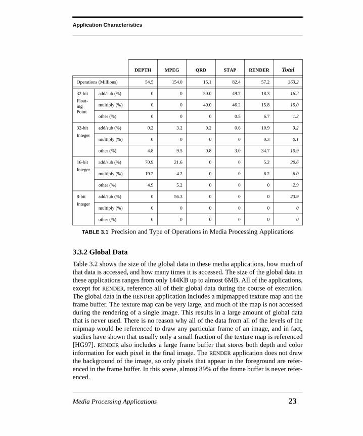
3.3.1 Operations
Table 3.1 shows the precision and type of operations performed by the media process-ing applications. The five applications perform between 15 and 154 million opera-tions over the course of their execution. The table shows the percentage of operationsin each application by precision and type. The types of operations are divided intothree categories: add/sub, multiply, and other. The add/sub category includes all addi-tion and subtraction operations. The multiply category includes all types of multipli-cation operations. Finally, the other category includes all other operations, such asdivide, shift and logical operations. The table shows that the bulk of these operationsare on low-precision data. For instance, over 56% of the operations performed byMPEG are 8-bit integer addition or subtraction operations.
Both DEPTH and MPEG perform only integer operations. Their data is mostly 8-bit and16-bit integers. A few 32-bit integer operations are performed, but these operationsare mostly for bookkeeping purposes and do not manipulate image data. In contrast,QRD and STAP perform mostly floating point operations. Again, a few 32-bit integeroperations are performed by these applications, but they are for bookkeeping pur-poses and do not manipulate media data. Even though these applications use floatingpoint data for its range, they still use low-precision data, as they are able to makeeffective use of single-precision (32-bit) floating point operations, instead of the dou-ble-precision (64-bit) operations found in many modern microprocessors.
The table shows that almost half of the operations performed collectively by theseapplications are 8-bit and 16-bit addition and subtraction operations. Most of the restof the operations are 32-bit floating point addition, subtraction, and multiplication.Therefore, the bulk of media operations found in these applications operate on low-precision integer and floating point data.
22 Stream Processor Architecture
Application Characteristics
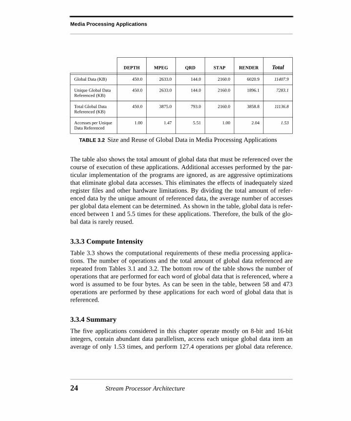
3.3.2 Global Data
Table 3.2 shows the size of the global data in these media applications, how much ofthat data is accessed, and how many times it is accessed. The size of the global data inthese applications ranges from only 144KB up to almost 6MB. All of the applications,except for RENDER, reference all of their global data during the course of execution.The global data in the RENDER application includes a mipmapped texture map and theframe buffer. The texture map can be very large, and much of the map is not accessedduring the rendering of a single image. This results in a large amount of global datathat is never used. There is no reason why all of the data from all of the levels of themipmap would be referenced to draw any particular frame of an image, and in fact,studies have shown that usually only a small fraction of the texture map is referenced[HG97]. RENDER also includes a large frame buffer that stores both depth and colorinformation for each pixel in the final image. The RENDER application does not drawthe background of the image, so only pixels that appear in the foreground are refer-enced in the frame buffer. In this scene, almost 89% of the frame buffer is never refer-enced.
DEPTH MPEG QRD STAP RENDER Total
Operations (Millions) 54.5 154.0 15.1 82.4 57.2 363.2
32-bit
Float-ing Point
add/sub (%) 0 0 50.0 49.7 18.3 16.2
multiply (%) 0 0 49.0 46.2 15.8 15.0
other (%) 0 0 0 0.5 6.7 1.2
32-bit
Integer
add/sub (%) 0.2 3.2 0.2 0.6 10.9 3.2
multiply (%) 0 0 0 0 0.3 0.1
other (%) 4.8 9.5 0.8 3.0 34.7 10.9
16-bit
Integer
add/sub (%) 70.9 21.6 0 0 5.2 20.6
multiply (%) 19.2 4.2 0 0 8.2 6.0
other (%) 4.9 5.2 0 0 0 2.9
8-bit
Integer
add/sub (%) 0 56.3 0 0 0 23.9
multiply (%) 0 0 0 0 0 0
other (%) 0 0 0 0 0 0
TABLE 3.1 Precision and Type of Operations in Media Processing Applications
Media Processing Applications 23
Media Processing Applications
The table also shows the total amount of global data that must be referenced over thecourse of execution of these applications. Additional accesses performed by the par-ticular implementation of the programs are ignored, as are aggressive optimizationsthat eliminate global data accesses. This eliminates the effects of inadequately sizedregister files and other hardware limitations. By dividing the total amount of refer-enced data by the unique amount of referenced data, the average number of accessesper global data element can be determined. As shown in the table, global data is refer-enced between 1 and 5.5 times for these applications. Therefore, the bulk of the glo-bal data is rarely reused.
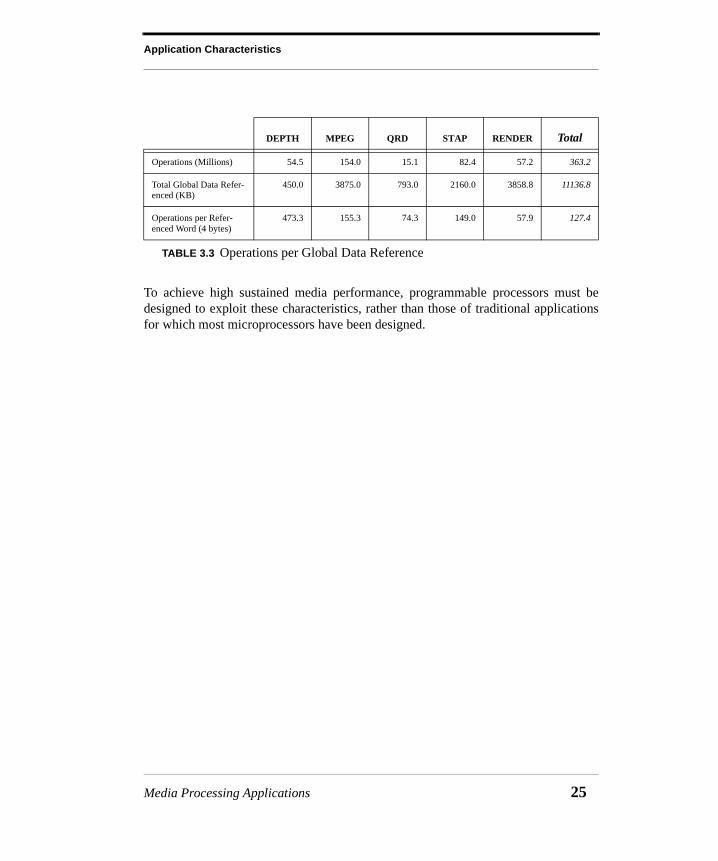
3.3.3 Compute Intensity
Table 3.3 shows the computational requirements of these media processing applica-tions. The number of operations and the total amount of global data referenced arerepeated from Tables 3.1 and 3.2. The bottom row of the table shows the number ofoperations that are performed for each word of global data that is referenced, where aword is assumed to be four bytes. As can be seen in the table, between 58 and 473operations are performed by these applications for each word of global data that isreferenced.
3.3.4 Summary
The five applications considered in this chapter operate mostly on 8-bit and 16-bitintegers, contain abundant data parallelism, access each unique global data item anaverage of only 1.53 times, and perform 127.4 operations per global data reference.
DEPTH MPEG QRD STAP RENDER Total
Global Data (KB) 450.0 2633.0 144.0 2160.0 6020.9 11407.9
Unique Global Data Referenced (KB)
450.0 2633.0 144.0 2160.0 1896.1 7283.1
Total Global Data Referenced (KB)
450.0 3875.0 793.0 2160.0 3858.8 11136.8
Accesses per Unique Data Referenced
1.00 1.47 5.51 1.00 2.04 1.53
TABLE 3.2 Size and Reuse of Global Data in Media Processing Applications
24 Stream Processor Architecture
Application Characteristics
To achieve high sustained media performance, programmable processors must bedesigned to exploit these characteristics, rather than those of traditional applicationsfor which most microprocessors have been designed.
DEPTH MPEG QRD STAP RENDER Total
Operations (Millions) 54.5 154.0 15.1 82.4 57.2 363.2
Total Global Data Refer-enced (KB)
450.0 3875.0 793.0 2160.0 3858.8 11136.8
Operations per Refer-enced Word (4 bytes)
473.3 155.3 74.3 149.0 57.9 127.4
TABLE 3.3 Operations per Global Data Reference
Media Processing Applications 25
Media Processing Applications
26 Stream Processor Architecture

CHAPTER 4 The Imagine Stream Processor
The Imagine stream processor is a programmable media processor designed to pro-cess data streams. Imagine is organized around a three-tiered data bandwidth hierar-chy consisting of a streaming memory system (2GB/s), a global stream register file(32GB/s), and a set of local distributed register files near the arithmetic units(544GB/s). This hierarchy therefore provides memory bandwidth, global registerbandwidth, and local register bandwidth with a ratio of 1:16:272. For each wordaccessed in memory, 16 words may be accessed in the global stream register file(SRF), and 272 words may be accessed in the clusters’ local register files. At the low-est level, the memory system is designed to maximize the bandwidth of stream datatransfers from external DRAM, rather than minimize the latency of individual refer-ences. The 128KB SRF at the center of the bandwidth hierarchy not only providesintermediate storage for data streams, but also enables additional stream clients to bemodularly connected to Imagine, such as a streaming network interface or a graphicstexture caching unit. At the highest level, local distributed register files feed 48 arith-metic units organized into a single-instruction, multiple-data (SIMD) array of eightidentical clusters. Imagine is designed to be a proof-of-concept stream processorshowing the viability of structures such as the bandwidth hierarchy and the streamingmemory system to enable scalable microprocessors that deliver high sustained multi-media performance. In a 0.15µm CMOS standard-cell implementation, Imagine willoperate at 500MHz, yielding a peak performance of 20GFLOPS on a 2.5cm2 chip.This chapter explains the Imagine architecture, its stream programming model, and itsscalability.
The Imagine Stream Processor 27

The Imagine Stream Processor
4.1 Stream Processing
Technology and application trends together motivate a shift away from the scalar,general-purpose register architecture in wide use today toward a stream-based archi-tecture with a bandwidth-efficient register organization. A 32-bit floating-point multi-plier requires less than 0.25mm2 of chip area in a contemporary 0.18µm CMOStechnology, so hundreds of arithmetic units can fit on an inexpensive 1cm2 chip. Thechallenge, however, is keeping these units fed with instructions and data. It is infeasi-ble to support tens to hundreds of arithmetic units with a single register file andinstruction issue unit. Therefore, partitioned structures that use local communicationare required to take advantage of the available computation resources.
Media processing applications, including rendering 2-D and 3-D graphics, image andvideo compression and decompression, and image processing, contain significantamounts of locality and concurrency. These applications operate on large streams oflow-precision integer data and share the following three key characteristics: opera-tions on elements within streams are data-parallel, global data is rarely reused, and asmany as 100-200 operations are performed per global data reference. These applica-tions are poorly matched to conventional architectures that exploit very little parallel-ism, depend on data reuse, and can perform very few operations per memoryreference.
Fortunately, these applications are well matched to the characteristics of modernVLSI technology. The data parallelism inherent in these applications allows a singleinstruction to control multiple arithmetic units and allows intermediate data to belocalized to small clusters of units, significantly reducing communication demands.Even though global data is rarely reused, forwarding streams of data from one pro-cessing kernel to the next localizes data communication. Furthermore, the computa-tion demands of these applications can be satisfied by keeping intermediate data closeto the arithmetic units, rather than in memory, and by organizing multiple arithmeticunits to take advantage of both data parallelism and instruction-level parallelism.
The Imagine architecture matches the demands of media applications to the capabili-ties of VLSI technology by supporting a stream programming model which exposesthe desired locality and concurrency within the applications. Imagine is organizedaround a large (128KByte) stream register file (SRF). Memory load and store opera-tions move entire streams of data between memory and the SRF. To the programmer,Imagine is a load/store architecture for streams; an application loads streams into theSRF, passes these streams through a number of computation kernels, and stores theresults back to memory.
28 Stream Processor Architecture
Stream Processing
This chapter describes the basic elements of the Imagine architecture and the streamprogramming model. It provides the basis for the in-depth explanation of the band-width hierarchy and memory access scheduling presented in Chapters 5 and 6. Imag-ine will also act as the baseline architecture for the experimental evaluation of thosefeatures.
4.1.1 Stream Programming
Media processing applications are naturally expressed as a sequence of computationkernels that operate on long data streams. A kernel is a small program that is repeatedfor each successive stream element in its input streams to produce output streams thatare fed to subsequent kernels. Each data stream is a variable length collection ofrecords, where each record is a logical grouping of media data. For example, a recordcould represent a triangle vertex in a polygon rendering application. A data stream,then, could be a collection of hundreds of these vertices.
Records within a data stream are accessed sequentially and processed identically. Thisgreatly simplifies the movement of data through a media processor by allowing theinstruction overhead to be amortized over the length of these homogeneous datastreams. For instance, a single memory stream transfer operation can collect hundredsof records from memory to form a homogeneous stream that is stored sequentially ina stream register file on the processor. This stream can then be transferred across thenetwork, again with a single instruction, or processed by a computation kernel.
By organizing media processing applications in this stream model, the followingcharacteristics that were enumerated in the previous chapter are exposed: data paral-lelism is abundant, very little data is reused, and many operations are required permemory reference. These properties can easily be exploited by a media processordesigned to operate on data streams. The abstraction of a data stream maps naturallyto the streaming data types found in media processing applications. The inputs tomost media processing applications are already data streams and the expected outputsare data streams as well. Streams expose the fine-grained data parallelism inherent inmedia applications as well. Each record of a stream, whether it is 8 bits or 24 words,will be processed identically, so multiple records can be processed in parallel usingthe same instructions.
Kernels naturally expose the coarse-grained control parallelism in media processingapplications, as they form a pipeline of tasks. Multiple kernels can therefore operatein parallel on different sections of the application’s data. The first kernel in the pipe-line would produce output streams that would then be passed to the next kernel. As
The Imagine Stream Processor 29
The Imagine Stream Processor
the next kernel operates on those streams, the original kernel could operate on thenext set of input data. Finally, the memory and network bandwidth demands of mediaprocessing applications can also be met using this stream model. Since all data isorganized as streams, single memory or network transfer operations initiate longtransfers with little control overhead that can be optimized for bandwidth.
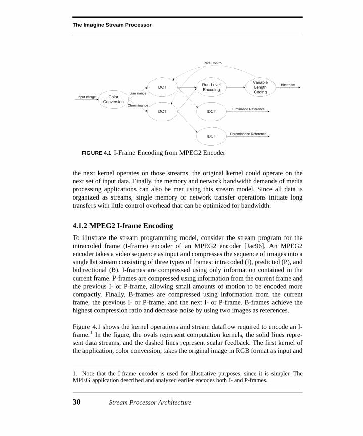
4.1.2 MPEG2 I-frame Encoding
To illustrate the stream programming model, consider the stream program for theintracoded frame (I-frame) encoder of an MPEG2 encoder [Jac96]. An MPEG2encoder takes a video sequence as input and compresses the sequence of images into asingle bit stream consisting of three types of frames: intracoded (I), predicted (P), andbidirectional (B). I-frames are compressed using only information contained in thecurrent frame. P-frames are compressed using information from the current frame andthe previous I- or P-frame, allowing small amounts of motion to be encoded morecompactly. Finally, B-frames are compressed using information from the currentframe, the previous I- or P-frame, and the next I- or P-frame. B-frames achieve thehighest compression ratio and decrease noise by using two images as references.
Figure 4.1 shows the kernel operations and stream dataflow required to encode an I-frame.1 In the figure, the ovals represent computation kernels, the solid lines repre-sent data streams, and the dashed lines represent scalar feedback. The first kernel ofthe application, color conversion, takes the original image in RGB format as input and
FIGURE 4.1 I-Frame Encoding from MPEG2 Encoder
1. Note that the I-frame encoder is used for illustrative purposes, since it is simpler. TheMPEG application described and analyzed earlier encodes both I- and P-frames.
ColorConversion
DCT
DCT IDCT
IDCT
Run-LevelEncoding
VariableLengthCoding
Input ImageLuminance
ChrominanceLuminance Reference
Chrominance Reference
Bitstream
Rate Control
30 Stream Processor Architecture

Stream Processing
generates two output streams: the luminance (Y) and the chrominance (CbCr) of theimage.
Each kernel depicted in Figure 4.1 is written in the KernelC language, described inSection 4.3.2. Figure 4.2 shows a simplified version of the color conversion kernel(convert).2 This kernel takes one input stream and produces two output streams, cor-responding directly to the streams indicated by the arrows in Figure 4.1. Figure 4.3graphically depicts the VLIW code for the color conversion kernel compiled by thekernel compiler, iscd [MDR+00]. For clarity, the preprocessing before the loop andthe postprocessing after the loop are not shown in either figure. In Figure 4.3, the col-umns are the functional units in the arithmetic clusters, the rows are instructions, andeach box indicates an operation. The box indicating each operation spans the appro-priate number of instructions given that particular operation’s latency. Since the unitsare pipelined, operations can overlap. Using a three-stage software pipeline and pro-cessing two pixels per loop iteration per cluster, this particular unoptimized kernelachieves 74% utilization of the adders and multipliers. KernelC eliminates the need toprogram in assembly, as this visualization of the compiled code can be used to drivesource code optimizations to improve kernel performance.
kernel convert(istream<RGB> RGB_pixels, ostream<Y> Y_pixels,ostream<CbCr> CbCr_pixels)
{RGB inPix;Y outY;CbCr outCbCr;
loop_stream(RGB_pixels) {// Input next pixelRGB_pixels >> inPix;
// Convert RGB to YCbCroutY = 0.257*inPix.r + 0.504*inPix.g + 0.098*inPix.b + 16;outCbCr.cb = -0.148*inPix.r - 0.291*inPix.g + 0.439*inPix.b + 128;outCbCr.cr = 0.439*inPix.r - 0.368*inPix.g - 0.071*inPix.b + 128;
// Output resulting pixelY_pixels << outY;CbCr_pixels << outCbCr;
}}
FIGURE 4.2 Color Conversion Kernel
2. The actual color conversion kernel also filters and subsamples the chrominance values.
The Imagine Stream Processor 31
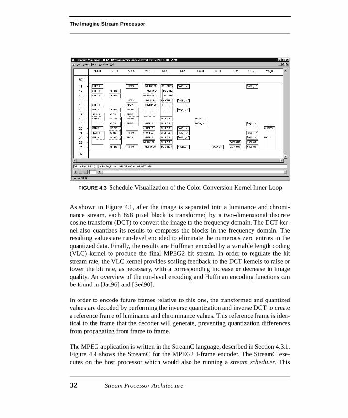
The Imagine Stream Processor
As shown in Figure 4.1, after the image is separated into a luminance and chromi-nance stream, each 8x8 pixel block is transformed by a two-dimensional discretecosine transform (DCT) to convert the image to the frequency domain. The DCT ker-nel also quantizes its results to compress the blocks in the frequency domain. Theresulting values are run-level encoded to eliminate the numerous zero entries in thequantized data. Finally, the results are Huffman encoded by a variable length coding(VLC) kernel to produce the final MPEG2 bit stream. In order to regulate the bitstream rate, the VLC kernel provides scaling feedback to the DCT kernels to raise orlower the bit rate, as necessary, with a corresponding increase or decrease in imagequality. An overview of the run-level encoding and Huffman encoding functions canbe found in [Jac96] and [Sed90].
In order to encode future frames relative to this one, the transformed and quantizedvalues are decoded by performing the inverse quantization and inverse DCT to createa reference frame of luminance and chrominance values. This reference frame is iden-tical to the frame that the decoder will generate, preventing quantization differencesfrom propagating from frame to frame.
The MPEG application is written in the StreamC language, described in Section 4.3.1.Figure 4.4 shows the StreamC for the MPEG2 I-frame encoder. The StreamC exe-cutes on the host processor which would also be running a stream scheduler. This
FIGURE 4.3 Schedule Visualization of the Color Conversion Kernel Inner Loop
32 Stream Processor Architecture
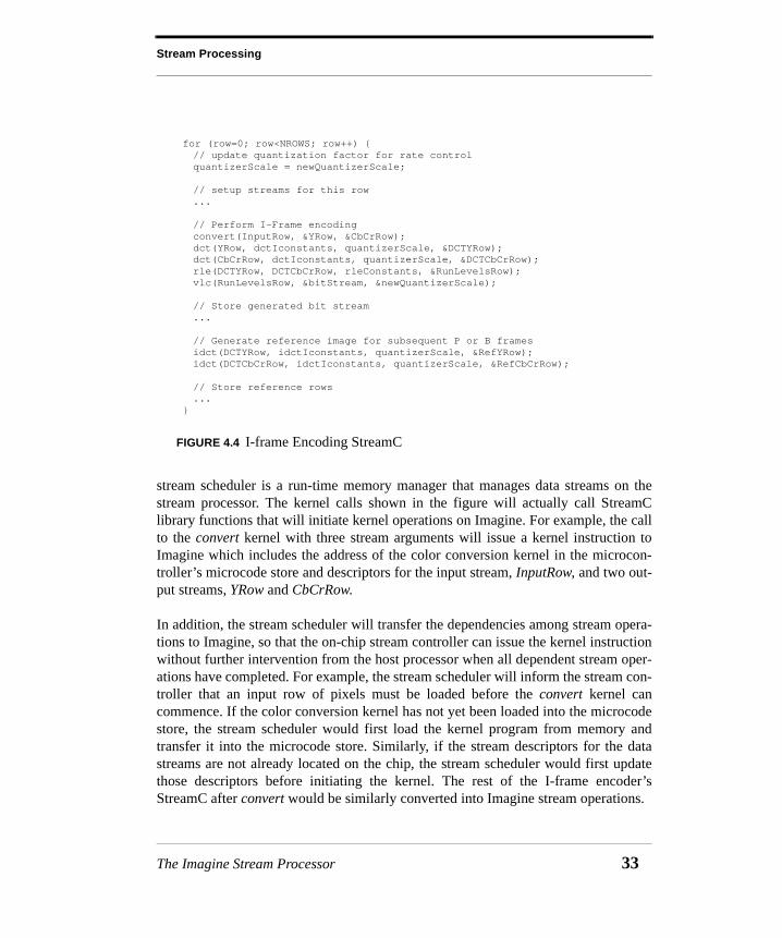
Stream Processing
stream scheduler is a run-time memory manager that manages data streams on thestream processor. The kernel calls shown in the figure will actually call StreamClibrary functions that will initiate kernel operations on Imagine. For example, the callto the convert kernel with three stream arguments will issue a kernel instruction toImagine which includes the address of the color conversion kernel in the microcon-troller’s microcode store and descriptors for the input stream, InputRow, and two out-put streams, YRow and CbCrRow.
In addition, the stream scheduler will transfer the dependencies among stream opera-tions to Imagine, so that the on-chip stream controller can issue the kernel instructionwithout further intervention from the host processor when all dependent stream oper-ations have completed. For example, the stream scheduler will inform the stream con-troller that an input row of pixels must be loaded before the convert kernel cancommence. If the color conversion kernel has not yet been loaded into the microcodestore, the stream scheduler would first load the kernel program from memory andtransfer it into the microcode store. Similarly, if the stream descriptors for the datastreams are not already located on the chip, the stream scheduler would first updatethose descriptors before initiating the kernel. The rest of the I-frame encoder’sStreamC after convert would be similarly converted into Imagine stream operations.
for (row=0; row<NROWS; row++) {// update quantization factor for rate controlquantizerScale = newQuantizerScale;
// setup streams for this row...
// Perform I-Frame encodingconvert(InputRow, &YRow, &CbCrRow);dct(YRow, dctIconstants, quantizerScale, &DCTYRow);dct(CbCrRow, dctIconstants, quantizerScale, &DCTCbCrRow);rle(DCTYRow, DCTCbCrRow, rleConstants, &RunLevelsRow);vlc(RunLevelsRow, &bitStream, &newQuantizerScale);
// Store generated bit stream...
// Generate reference image for subsequent P or B framesidct(DCTYRow, idctIconstants, quantizerScale, &RefYRow);idct(DCTCbCrRow, idctIconstants, quantizerScale, &RefCbCrRow);
// Store reference rows...
}
FIGURE 4.4 I-frame Encoding StreamC
The Imagine Stream Processor 33

The Imagine Stream Processor
This I-frame encoder illustrates the three key properties of media processing applica-tions mentioned earlier: very little data is reused, data parallelism is abundant, andmany operations are required per memory reference. First, data is rarely reused in thisapplication; for example, once the image is color converted, the original input imageis never referred to again. Second, most computations within the encoder are data par-allel. If there were enough hardware, all of the blocks in the image could be color con-verted in parallel, since there is no dependence from one block to another. Finally,assuming that only the original image, the final coded bit stream, and the referenceimages are actually stored in memory, this I-frame encoder would perform 49.5 arith-metic operations per memory reference.
4.2 Architecture
The stream architecture of the Imagine media processor effectively exploits the desir-able application characteristics exposed by the stream model. Imagine meets the com-putation and bandwidth demands of media applications by directly processing thenaturally occurring data streams within these applications. Figure 4.5 shows a blockdiagram of Imagine’s microarchitecture. Imagine is designed to be a coprocessor thatoperates on multimedia data streams. The stream register file (SRF) effectively iso-
FIGURE 4.5 Imagine Block Diagram
Imagine Stream Processor
Stream Register FileNetworkInterface
StreamController
Streaming Memory System
AL
U C
lust
er 0
AL
U C
lust
er 7
AL
U C
lust
er 6
AL
U C
lust
er 5
AL
U C
lust
er 4
AL
U C
lust
er 3
AL
U C
lust
er 2
AL
U C
lust
er 1
Mic
roco
ntro
ller
SDRAM SDRAMSDRAM SDRAM
Net
wor
kHostProcessor
34 Stream Processor Architecture
Architecture
lates the arithmetic units from the memory system, making Imagine a load/storearchitecture for streams. All stream operations transfer data streams to or from theSRF. For instance, the network interface transfers streams directly out of and into theSRF, isolating network transfers from memory accesses and computation. This sim-plifies the design of the processor and allows the clients (the arithmetic clusters, thememory system, the network interface, etc.) to tolerate the latency of other stream cli-ents. In essence, the SRF enables the streaming data types inherent in media process-ing applications to be routed efficiently throughout the processor.
As shown in Figure 4.5, eight arithmetic clusters, a microcontroller, a streamingmemory system, a network interface, and a stream controller are connected to theSRF. The arithmetic clusters consume data streams from the SRF, process them, andreturn their output data streams to the SRF. The microcontroller is connected to theSRF to allow compiled kernel programs to be loaded from the SRF into the microcon-troller’s microcode store. The streaming memory system transfers streams betweenthe SRF and the off-chip DRAM. The network interface transfers streams between theSRF and other processors or devices connected to the network. The stream controllerallows the host processor to transfer data and microcode programs into or out of theSRF, although large data transfers would be made through the Imagine network.
4.2.1 Stream Register File (SRF)
The SRF is a 128KB (1Mbit) memory optimized for stream transfers. The SRF canhold multiple variable-length data streams, subject only to capacity constraints. Adata stream is an arbitrary length sequence of records, such as a row of pixels from animage or a set of vertices from a polygonal graphics model. Streams are referencedusing stream descriptors which are held in a 64-entry stream descriptor register file(SDRF). Each stream descriptor register (SDR) includes a base address in the SRFand a stream length. The memory array of the SRF has 1024 rows of 1024 bits with asingle port.
The stream register file supports numerous clients, including the arithmetic clustersand memory system, through a single physical port. However, each has its own dedi-cated logical port(s) into the SRF. To support this abstraction, all clients are connectedto the SRF by stream buffers. Each stream buffer is composed of two 1024-bit half-buffers. A half-buffer of a single stream buffer may be filled or drained each cyclethrough the 1024-bit port into the SRF memory array. If a stream buffer that is sup-porting a client reading from the SRF has an empty half-buffer, then that streambuffer requests access to the memory array. Similarly, if a stream buffer that is sup-porting a client writing to the SRF has a full half-buffer, then it also requests access to
The Imagine Stream Processor 35
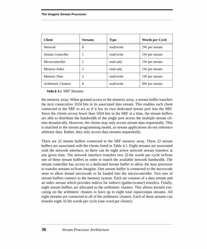
The Imagine Stream Processor
the memory array. When granted access to the memory array, a stream buffer transfersthe next consecutive 1024 bits in its associated data stream. This enables each clientconnected to the SRF to act as if it has its own dedicated stream port into the SRF.Since the clients access fewer than 1024 bits in the SRF at a time, the stream buffersare able to distribute the bandwidth of the single port across the multiple stream cli-ents dynamically. However, the clients may only access stream data sequentially. Thisis matched to the stream programming model, as stream applications do not referencearbitrary data. Rather, they only access data streams sequentially.
There are 22 stream buffers connected to the SRF memory array. These 22 streambuffers are associated with the clients listed in Table 4.1. Eight streams are associatedwith the network interface, so there can be eight active network stream transfers atany given time. The network interface transfers two 32-bit words per cycle to/fromone of these stream buffers in order to match the available network bandwidth. Thestream controller has access to a dedicated stream buffer to allow the host processorto transfer streams to/from Imagine. One stream buffer is connected to the microcodestore to allow kernel microcode to be loaded into the microcontroller. Two sets ofstream buffers connect to the memory system. Each set consists of a data stream andan index stream which provides indices for indirect (gather/scatter) transfers. Finally,eight stream buffers are allocated to the arithmetic clusters. This allows kernels exe-cuting on the arithmetic clusters to have up to eight total input/output streams. Alleight streams are connected to all of the arithmetic clusters. Each of these streams cantransfer eight 32-bit words per cycle (one word per cluster).
Client Streams Type Words per Cycle
Network 8 read/write 2W per stream
Stream Controller 1 read/write 1W per stream
Microcontroller 1 read only 1W per stream
Memory Index 2 read only 1W per stream
Memory Data 2 read/write 1W per stream
Arithmetic Clusters 8 read/write 8W per stream
TABLE 4.1 SRF Streams
36 Stream Processor Architecture

Architecture
4.2.2 Arithmetic Clusters
Imagine contains eight arithmetic clusters controlled by a single microcontroller in aSIMD fashion. The arithmetic clusters operate simultaneously on interleaved datarecords transferred from the SRF, allowing eight data records to be processed in paral-lel. As shown in Figure 4.6, each arithmetic cluster contains three adders, two multi-pliers, one divide/square root unit, one 256-entry scratch-pad memory, and oneintercluster communication unit. These units are controlled by statically scheduledVLIW instructions issued by the microcontroller. Across the eight arithmetic clusters,Imagine’s 48 arithmetic units achieve the high sustained computation rates requiredby media processing applications. The mix of arithmetic units in Imagine are matchedto the demands of the targeted media applications, but the architectural concept iscompatible with other mixes of arithmetic units within the clusters.
All of the arithmetic units support both 32-bit single precision floating point and 32-bit integer operations. In addition, the adders and multipliers also support 16-bit and8-bit parallel-subword operations for a subset of the integer operations. These arith-metic operations are well-matched to the low-precision data types commonly found inmedia processing applications. These parallel-subword instructions, similar to themultimedia instructions commonly added to general-purpose processors [Lee96][PW96] [TONH96], exploit the fine-grained data parallelism inherent in media appli-cations. The adders, multipliers, scratch-pad, and communication unit are fully pipe-lined, allowing a new operation to issue every cycle. The divide/square root unit hastwo SRT cores, so no more than two divide or square root operations can be in flightat any given time.
Data cannot be transferred directly from memory to the arithmetic clusters. All datafrom memory must first be loaded into the SRF and then transferred to the arithmetic
FIGURE 4.6 Arithmetic Cluster
+ /**++ Comm.Unit
Inte
rclu
ster
Net
wo
rk
To SRF
From SRF
Scratch-Pad
Cross Point
The Imagine Stream Processor 37
The Imagine Stream Processor
clusters. Sometimes, however, kernels executing in the arithmetic clusters benefitfrom being able to index into small arrays or lookup tables. The scratch-pad units ineach cluster provide this functionality; they are accessed with a base address providedby the microcontroller added to an offset provided locally by each cluster. Thisenables each cluster to access different array elements within its scratch-pad.
Rather than the conventional centralized register file organization, the arithmetic unitsutilize a distributed register file (DRF) structure. As shown in Figure 4.6, each arith-metic unit has a small dedicated two-port register file connected to each of its inputs.A switch then connects the outputs of all of the arithmetic units to the 17 register fileswithin the cluster. Effectively, the DRF organization eliminates the implicit switchthat would be replicated within each register of a conventional register file. Only oneexplicit switch is needed in the DRF organization. The cross points in Figure 4.6show where connections from the outputs of arithmetic units to register files can bemade. On the Imagine chip there is enough area over the arithmetic cluster to allow acomplete switch, so all of the cross points are connected. However, a sparse intercon-nect could be used and is fully supported by the compiler tools [MDR+00]. By mak-ing the communication among arithmetic units explicit through this switch, ratherthan implicit through a centralized register file, the area, delay, and power dissipationof the register file structure is drastically reduced with only a slight degradation inperformance [MDR+00] [RDK+00b].
Media applications are not always perfectly data parallel, and in fact often requireextensive data reorganization. To facilitate this reorganization, the communicationunit, shown on the right of Figure 4.6, allows data to be transferred among arithmeticclusters through the intercluster network, whereas the intracluster switch of the DRForganization only allows data to be communicated among arithmetic units within acluster. The communication unit within each cluster is able to drive one word percycle onto its own dedicated bus. The microcontroller also has a dedicated bus ontowhich it can drive data, to allow immediates and other data to be broadcast to theclusters. Collectively, these buses form the intercluster network, shown in Figure 4.7.Each cluster’s communication unit may read from any one of these nine buses eachcycle. A permutation descriptor controls which bus will be read by the communica-tion units in each cluster. This descriptor can either be provided globally by themicrocontroller or generated locally within each cluster. The ability to communicateamong the arithmetic clusters significantly improves performance of applications thatare not perfectly data-parallel, since each cluster may only access one eighth of thememory in the SRF.
38 Stream Processor Architecture

Architecture
4.2.3 Microcontroller
The microcontroller is a very long instruction word (VLIW) control engine that issuesinstructions to the arithmetic clusters. Each cycle, the microcontroller broadcasts asingle 568-bit VLIW instruction to all eight clusters. Since instructions are staticallyscheduled by the compiler, the only dynamic behavior is that the microcontroller maybe forced to stall the arithmetic clusters when a stream buffer is not ready for a clusteraccess. This occurs when the kernel attempts a stream input from an empty streambuffer or a stream output to a full stream buffer. In both of these cases, the microcon-troller stalls the arithmetic clusters until that stream buffer receives access to the SRFmemory array and is consequently made ready for cluster accesses.
Kernels are stored in a 2K instruction by 568 bit (1.1Mbit) microcode store locatedwithin the microcontroller. The microcontroller takes advantage of the high instruc-tion reference locality in small loops found in media processing applications by stor-ing kernels directly in this microcode store, rather than fetching them from memoryor a cache. Consequently, kernel instructions are never fetched from memory duringthe course of kernel execution, so kernels never need to stall due to instruction fetchlatencies. Frequently, the microcode store is large enough to hold all of the kernels foran application. In this case, kernels only need to be loaded once from memory for theentire execution of the application. However, if the kernels do not all fit, then they areloaded into the microcode store prior to their execution. In this case, the loading ofone kernel can be overlapped with the execution of other kernels in the application.
FIGURE 4.7 Intercluster Communication Network
Comm.Unit
Cluster 0
Comm.Unit
Cluster 1
Comm.Unit
Cluster 2
Comm.Unit
Cluster 3
Comm.Unit
Cluster 4
Comm.Unit
Cluster 5
Comm.Unit
Cluster 6
Comm.Unit
Cluster 7
Microcontroller
The Imagine Stream Processor 39

The Imagine Stream Processor
4.2.4 Streaming Memory System
The memory system supports data stream transfers between the SRF and off-chipDRAM. This stream load/store architecture simplifies programming and minimizesstalling in the arithmetic clusters by isolating them from variable memory accesslatencies. Because the granularity of memory references is streams of data and notindividual words, the memory system can be optimized for throughput, rather thanreference latency, which will be explored further in Chapter 6. Furthermore, accessesto external DRAM can be reordered to maximize the sustained bandwidth of the off-chip memory. Since a consumer of a stream, such as a kernel executing in the arith-metic clusters, cannot commence until the entire stream is available in the SRF, thetime it takes to load the entire stream is far more important than the latency of anyparticular reference. Moreover, these references can easily be overlapped with com-putation. The memory system can be loading streams for the next set of computationsand storing streams for the previous set of computations while the current set of com-putations is occurring.
As shown in Figure 4.8, the Imagine streaming memory system consists of a pair ofaddress generators, four interleaved memory banks, and a pair of reorder buffers thatplace stream data in the SRF in the correct order. All of these units are on the samechip as the Imagine processor core, except for the off-chip SDRAM memory.
FIGURE 4.8 Streaming Memory System
MemoryBank 0
SDRAM
MemoryBank 1
SDRAM
MemoryBank 2
SDRAM
MemoryBank 3
SDRAM
SRF
AddressGenerator 0
AddressGenerator 1
ReorderBuffer 0
ReorderBuffer 1
Inde
x
Inde
x
Dat
a
Dat
a
Processor Chip
Off-chip Memory
40 Stream Processor Architecture
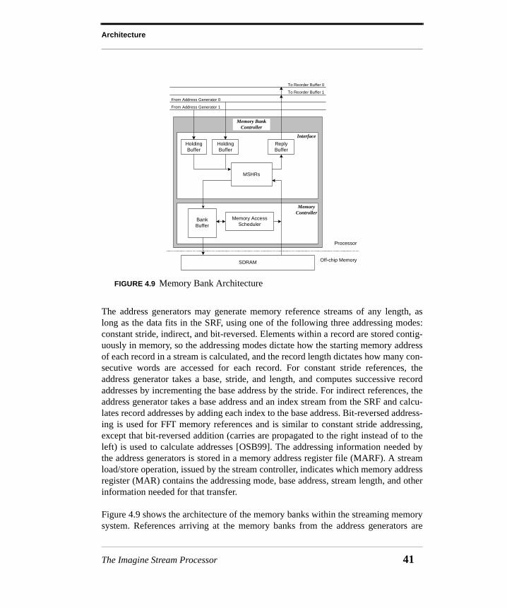
Architecture
The address generators may generate memory reference streams of any length, aslong as the data fits in the SRF, using one of the following three addressing modes:constant stride, indirect, and bit-reversed. Elements within a record are stored contig-uously in memory, so the addressing modes dictate how the starting memory addressof each record in a stream is calculated, and the record length dictates how many con-secutive words are accessed for each record. For constant stride references, theaddress generator takes a base, stride, and length, and computes successive recordaddresses by incrementing the base address by the stride. For indirect references, theaddress generator takes a base address and an index stream from the SRF and calcu-lates record addresses by adding each index to the base address. Bit-reversed address-ing is used for FFT memory references and is similar to constant stride addressing,except that bit-reversed addition (carries are propagated to the right instead of to theleft) is used to calculate addresses [OSB99]. The addressing information needed bythe address generators is stored in a memory address register file (MARF). A streamload/store operation, issued by the stream controller, indicates which memory addressregister (MAR) contains the addressing mode, base address, stream length, and otherinformation needed for that transfer.
Figure 4.9 shows the architecture of the memory banks within the streaming memorysystem. References arriving at the memory banks from the address generators are
FIGURE 4.9 Memory Bank Architecture
HoldingBuffer
HoldingBuffer
MSHRs
ReplyBuffer
BankBuffer
Memory AccessScheduler
Memory BankController
Interface
MemoryController
SDRAM
From Address Generator 1
From Address Generator 0
To Reorder Buffer 0
To Reorder Buffer 1
Processor
Off-chip Memory
The Imagine Stream Processor 41

The Imagine Stream Processor
stored in a small holding buffer until they can be processed. Despite the fact that thereis no cache, a set of registers similar in function to the miss status holding registers(MSHRs) of a non-blocking cache [Kro81] exist to keep track of in-flight referencesand to do read and write coalescing. When a reference arrives for a location that isalready the target of another in-flight reference, the MSHR entry for that reference isupdated to reflect that this reference will be satisfied by the same DRAM access.When a reference to a location that is not already the target of another in-flight refer-ence arrives, a new MSHR is allocated and the reference is sent to the bank buffer.The memory controller schedules DRAM accesses to satisfy the pending referencesin the bank buffer and returns completed accesses to the MSHRs. The MSHRs sendcompleted loads to a reply buffer which holds them until they can be sent back to thereorder buffers. As the name implies, the reorder buffers receive out of order refer-ences and transfer the data to the SRF in order.
In this streaming memory system, memory consistency is maintained in the followingtwo ways: conflicting memory stream references are issued in dependency order, andthe MSHRs ensure that references to the same address complete in the order that theyarrive. This means that a stream load that follows a stream store to overlapping mem-ory locations may be issued as soon as the address generators have sent all of thestore’s references to the memory banks.
4.2.5 Network Interface
The network interface connects the SRF of the Imagine stream processor to an exter-nal network, enabling source routed data stream transfers through that network.Source routing information is held in a network route register file (NRRF) within thenetwork interface. Each network route register (NRR) can be written with a sourceroute that can then be used to control the path taken by network stream transfers. Thenetwork interface transfers entire data streams from one processor to another throughthe Imagine network. This drastically increases the ratio of data to control that mustgo through the network, as well as eliminating instructions to send and receive eachdata element within the stream.
The Imagine processor has four bidirectional network channels that can be intercon-nected in an arbitrary topology. Each channel is 16-bits wide in each direction anduses differential signaling, requiring a total of 256 data pins in the network interface.Not only can other Imagine processors be connected to the external network, but I/Odevices can also be connected to the network, with some additional logic, to send andreceive streams using the Imagine network protocol. Since the channels may be inter-connected in an arbitrary topology, multiprocessor solutions can be constructed that
42 Stream Processor Architecture

Architecture
provide network bandwidth tailored to the communication demands of the targetedapplications. For instance, all four channels of two Imagine processors could be con-nected to each other to provide four times the network bandwidth between those twoprocessors. This flexible topology combined with the amortization of instructions andcontrol over entire data streams enable Imagine to deliver the high network band-width demanded by media processing applications.
4.2.6 Stream Controller
The stream controller receives stream instructions from the host processor and issuesthem to the units of Imagine, described in Sections 4.2.1-4.2.5, subject to dependencyconstraints. The stream controller is similar in function to the issue unit in a supersca-lar processor; it issues stream instructions, possibly out of order, to available streamunits without violating the dependencies among stream instructions. The stream con-troller accepts instructions from the host processor, stores them in a pending instruc-tion queue, and determines which instructions are available for issue. Status signalsfrom the stream units are used to determine when operations complete, allowing thestream controller to know when an instruction’s dependencies have been satisfied.The stream controller simply selects an instruction that is ready to issue and issues itto the appropriate stream unit. The stream controller also includes a general-purposeregister file (SCTRF) that can be accessed by stream register read, write, and moveinstructions, which will be described in Section 4.3.1. These registers are used totransfer data between the stream controller and other modules, such as the host pro-cessor or control registers within the stream units.
4.2.7 Host Processor
An external host processor executes all scalar code and transfers stream instructionsto Imagine, which acts as a coprocessor. A stream processor could include a serialhost processor on the same chip. This would allow the two processors to be tightlyintegrated so that the overhead of issuing instructions to the stream processor wouldbe negligible. However, since Imagine is a proof-of-concept research project, an off-the-shelf host processor is used to control Imagine. The host processor is able to exe-cute small serial sections of code that exist in any real-world application. Imagine istailored to take advantage of the characteristics of media processing applications, asdescribed in Chapter 3. Code that is not actually operating on media data, but is ratherorchestrating the control flow of the overall application, is much better suited to aconventional serial processor than a SIMD stream processor like Imagine. Therefore,
The Imagine Stream Processor 43

The Imagine Stream Processor
each processor is able to execute the code for which it was designed — the host pro-cessor executes small sections of control intensive serial code and Imagine executeslarge data parallel stream programs.
4.3 Programming Model
The stream programming model exposes the following three key properties of mediaprocessing applications: very little data is reused, data parallelism is abundant, andmany arithmetic operations are required per memory reference. In media processingapplications expressed in this form, most data is passed directly from kernel to kernelthrough data streams. Kernels are usually perfectly data-parallel, or nearly so, allow-ing multiple stream elements to be processed simultaneously. Finally, data streamscan be recirculated from one kernel to the next through the SRF, without requiringdata to be returned to memory for intermediate storage.
Stream applications are programmed at two levels: stream and kernel. As described inSection 4.2.7, a stream processor acts as a coprocessor to a sequential host processor.Stream-level programs execute on this host processor and orchestrate the flow of datastreams through the stream processor. These programs are written in StreamC, aderivative of C++ that includes library functions that issue stream instructions to thestream processor. Kernel-level programs operate on these data streams and execute onthe microcontroller and arithmetic clusters of the stream processor. Kernels are writ-ten in KernelC, a subset of the C language, and may access local variables, read thehead elements of input streams, and write the tail elements of output streams. Kernelsmay not, however, make arbitrary memory references. Kernels loop over their inputstreams, perform computations on each stream record element in turn, and producesuccessive data elements of their output streams.
4.3.1 Stream-level Programming
StreamC programs make calls to library functions in order to manipulate streams onthe stream processor. These library functions can send operations to the stream pro-cessor from the stream instruction set, which includes the eleven basic instructions inTable 4.2. All of the instructions, except READ, are asynchronous, in that the host pro-cessor may issue them to the stream processor and then continue execution of thestream program. The host processor must wait for the return value of the READ
instruction. The stream instructions can be grouped into the following four categories:control word movement, synchronization, stream movement, and computation.
44 Stream Processor Architecture

Programming Model
Control Word Movement. The MOVE, WRITE_IMM, and READ instructions allow thehost processor to transfer control information to/from the non-cluster registers on thestream processor. The MOVE instruction allows data values to be moved from one reg-ister to another. This is useful if one stream instruction generates a value that will beused by another stream instruction. The WRITE_IMM instruction writes a value to aregister in the stream processor. The READ instruction similarly reads a value from aregister in the stream processor. The target of these three instructions are usually themicrocontroller register file (UCRF), the stream descriptor register file (SDRF), the
Instruction Description
MOVE dst_reg src_reg Move the contents of src_reg to dst_reg
WRITE_IMM reg data Write data into reg
READ reg Return the contents of reg to the host processor
barrier Block all subsequent instructions from issuing until all previ-ous instructions have issued
synch Synchronize microcontroller with stream controller
LOAD mar dat_sdr idx_sdr Load a stream from memory described by mar into a stream in the SRF described by dat_sdr — idx_sdr describes an index stream in the SRF for indexed loads
STORE mar dat_sdr idx_sdr Store a stream from the SRF described by dat_sdr to mem-ory described by mar — idx_sdr describes an index stream in the SRF for indexed store
SEND nrr tag sdr Send a stream from the SRF described by sdr to the network using the route held in nrr and identified by tag
RECEIVE tag sdr Receive a stream from the network identified by tag into a stream in the SRF described by sdr
LOAD_UCODE mpc sdr Load microcode program from a stream in the SRF described by sdr to location mpc in the microcode store
CLUSTOP mpc sdr0..sdr7 Initiate a kernel on the arithmetic clusters starting at location mpc in the microcode store — sdr0-sdr7 describe the input/output data streams in the SRF
TABLE 4.2 Imagine Stream Instruction Set Architecture
The Imagine Stream Processor 45

The Imagine Stream Processor
memory address register file (MARF), the network route register file (NRRF), and thestream controller register file (SCTRF), described in Section 4.2.
Synchronization. The BARRIER and SYNCH instructions enable the stream controller,host processor, and microcontroller to synchronize with each other. The host proces-sor sends a BARRIER instruction to indicate that all instructions that were sent prior tothe barrier instruction should issue before any instruction that was sent after the bar-rier instruction is issued. The SYNCH instruction synchronizes the stream controllerwith the microcontroller, leaving other stream transfers unaffected. When a kernelissues a synchronization instruction, the microcontroller stalls and the stream control-ler is notified that the microcontroller is waiting for a SYNCH instruction to resumeexecution. While the microcontroller is stalled, the stream controller can perform anynumber of stream operations, such as transferring information to or from the micro-controller through the UCRF. When the stream controller is done issuing the requiredstream operations, it issues the SYNCH instruction, which frees the microcontroller tocontinue execution.
Stream Movement. The LOAD, STORE, SEND, and RECEIVE instructions transfer datastreams throughout the system. LOAD and STORE instructions move data streamsbetween the SRF and memory. These instructions take a stream descriptor (dat_sdr)which specifies a starting location and length of a stream in the SRF, and an addressdescriptor (mar) that provides the base address in memory, addressing mode (constantstride, indexed, or bit-reversed), and the record size of data elements in the stream.Indexed memory transfers take an additional stream descriptor (idx_sdr) which speci-fies the start and length of the index stream in the SRF. SEND and RECEIVE instructionsallow streams to be transferred from the SRF of one Imagine processor to the SRF ofanother Imagine processor through the network. SEND and RECEIVE instructions canalso be used for I/O transfers through the network.
Computation. Finally, the CLUSTOP instruction initiates a kernel operation on a set ofdata streams. This instruction specifies a kernel to execute using an address into theon-chip microcode storage (mpc) and stream descriptors for up to eight input and/oroutput streams in the SRF (sdr0-sdr7). Kernels are loaded from the SRF (they are firstloaded from memory into the SRF using a normal stream LOAD instruction) to themicrocode store by a LOAD_UCODE instruction. If the microcode storage is largeenough to hold all of the kernels needed by an application (as it frequently is), theneach kernel need only be loaded into the microcode store once and may then bereused by subsequent CLUSTOP instructions.
46 Stream Processor Architecture

Programming Model
4.3.2 Kernel-level Programming
KernelC programs are written in a subset of the C language. All C mathematicalexpressions are supported, but pointers are not allowed and the control flow con-structs are restricted. The C++ stream operators, >> and <<, are used to read recordsinto the clusters from input streams and write records to output streams in the SRF.Kernels are optimized for stream computation, so they may not use pointers to makearbitrary memory references. To allow limited memory addressing, either an indexstream can be generated that can be used to perform an indirect stream load or store,or small arrays may be stored within the clusters’ scratch-pads. All instructions in aKernelC program are executed simultaneously on all eight clusters, thereby process-ing eight stream elements identically in parallel. On such a SIMD machine, datadependent control flow constructs, such as if-then-else, are not allowed. The onlyform of control flow allowed in a KernelC program is a loop which can be terminatedby a variety of conditions, such as a counter in the microcontroller or a combinationof cluster condition codes.
A KernelC program must be written with the knowledge that it will execute simulta-neously on all eight clusters, since the Imagine compiler tools do not currently per-form automatic SIMD parallelization. Because this parallelization is not automatic,the programmer must orchestrate the movement of data between the arithmetic clus-ters. A typical kernel will be written to first perform some preprocessing, then loopover its input stream(s), and finally perform some postprocessing. The preprocessingstage typically consists of setting up constants and reading in coefficients from SRFstreams. The main loop will then process eight elements of the kernel’s inputstream(s) per iteration. This loop can be unrolled and/or software pipelined toimprove performance. If the kernel operation is completely data-parallel, the loopsimply reads its inputs, performs some processing, and writes its outputs. However,many media processing kernels involve some interaction among stream elements.Consequently, the main loop may require communication among the clusters and/orstorage of previous stream elements. A set of communication instructions exist inKernelC to transfer data among the clusters. These instructions compile to operationsthat are executed by the communication units in the clusters. Finally, the post process-ing stage performs any end-case cleanup that is necessary for the kernel. Kernels,however, do not need to follow this structure since KernelC is flexible enough toallow multiple loops or nested loops, as the algorithm requires.
Despite the abundant data parallelism available in media processing applications, datadependent conditional control flow is sometimes necessary. Since the clusters operatein a SIMD fashion, such data dependent conditional execution can be difficult. Imag-ine provides the following three mechanisms that convert data dependent control flow
The Imagine Stream Processor 47
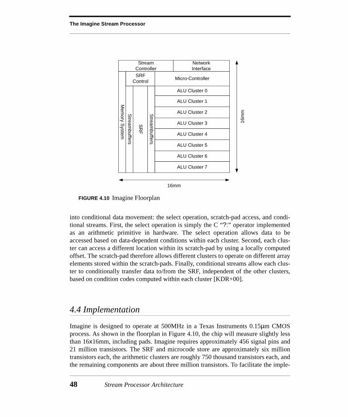
The Imagine Stream Processor
into conditional data movement: the select operation, scratch-pad access, and condi-tional streams. First, the select operation is simply the C “?:” operator implementedas an arithmetic primitive in hardware. The select operation allows data to beaccessed based on data-dependent conditions within each cluster. Second, each clus-ter can access a different location within its scratch-pad by using a locally computedoffset. The scratch-pad therefore allows different clusters to operate on different arrayelements stored within the scratch-pads. Finally, conditional streams allow each clus-ter to conditionally transfer data to/from the SRF, independent of the other clusters,based on condition codes computed within each cluster [KDR+00].
4.4 Implementation
Imagine is designed to operate at 500MHz in a Texas Instruments 0.15µm CMOSprocess. As shown in the floorplan in Figure 4.10, the chip will measure slightly lessthan 16x16mm, including pads. Imagine requires approximately 456 signal pins and21 million transistors. The SRF and microcode store are approximately six milliontransistors each, the arithmetic clusters are roughly 750 thousand transistors each, andthe remaining components are about three million transistors. To facilitate the imple-
FIGURE 4.10 Imagine Floorplan
Micro-Controller
Stream
buffers
SR
F
Stream
buffers
Mem
ory System
SRFControl
StreamController
NetworkInterface
16m
m
16mm
ALU Cluster 0
ALU Cluster 1
ALU Cluster 2
ALU Cluster 3
ALU Cluster 4
ALU Cluster 5
ALU Cluster 6
ALU Cluster 7
48 Stream Processor Architecture

Implementation
mentation of a research prototype, not all of the chip need run at 500MHz. In fact,many units are designed such that they can run slower with negligible performancedegradation.
At the base of the bandwidth hierarchy, the memory system can supply 2GB/s of peakdata bandwidth. The four memory banks are each attached to their own external 32-bit wide SDRAMs. The memory controllers and SDRAMs operate at 125MHz, yield-ing a peak memory bandwidth of 500MB/s per bank. Data can also be fed into theSRF from the network. The network interface has a peak bandwidth of 8GB/s. Thefour 16-bit network channels operate at 500MHz, yielding a peak bandwidth of1GB/s per channel in each direction.
In the center of the bandwidth hierarchy, the 128KB SRF memory array is designed tooperate at 250MHz, yielding a peak bandwidth of 32GB/s. The 22 stream buffers,however, operate at 500MHz, yielding instantaneous peak bandwidth of 172GB/s.The stream buffers therefore scale the SRF bandwidth to enable short bursts of higherbandwidth than the 32GB/s memory array can provide. In practice, the clients rarelyneed an average bandwidth of more than the 32GB/s supplied by the memory array.
Finally, the arithmetic clusters contain 48 total arithmetic units (6 per cluster) and 136local register files (17 per cluster) that yield a peak computation rate of 20GFLOPSand a peak data bandwidth of 544GB/s. The clusters’ peak computation rate is20GOPS for both 32-bit integer or floating-point operations. For 16-bit and 8-bit par-allel-subword operations, the peak performance increases to 40 and 80GOPS, respec-tively.
The three-tiered bandwidth hierarchy of Imagine therefore provides DRAM band-width, global register bandwidth, and local register bandwidth with a ratio of1:16:272. That is, for each word accessed in memory, 16 words may be accessed inthe SRF, and 272 words may be accessed in the clusters' local register files. Vieweddifferently, Imagine can perform forty 32-bit arithmetic operations per 4-byte wordaccessed in memory, or 2.5 operations per word accessed in the SRF. This is well-matched to the compute intensive nature of media processing applications. For com-parison, conventional architectures can typically perform about five operations perword accessed in memory, and require three global register accesses per operation[HL99] [Kes99].
The Imagine Stream Processor 49
The Imagine Stream Processor
4.5 Scalability and Extensibility
Media processing applications currently demand very high computation rates, and asmedia processing algorithms and applications become more realistic and sophisti-cated those rates will continue to increase. Therefore, any useful media processormust be able to scale beyond its current capabilities. The modularity of the Imaginearchitecture easily lends itself to scaling and extension. Internally, the Imagine pro-cessor can easily be scaled or extended, as the SRF isolates the various stream unitsfrom each other. The SRF also allows new stream clients to be added to the processorwithout disrupting the rest of the architecture. The network interface allows multipleImagine processors to be interconnected without disrupting the programming model.Applications that run on a single Imagine processor can be ported to a multiprocessorconfiguration by inserting network send and receive instructions. These instructionstransfer streams from one processor to the next in the middle of the kernel processingpipeline.
4.5.1 Scalability
The number of arithmetic clusters can be increased or reduced in order to providehigher or lower stream throughput with a corresponding change in cost. The width ofthe SRF and the peak memory bandwidth also needs to be scaled equivalently tomaintain the correct bandwidth ratios to keep the arithmetic units’ utilization high.While increasing the number of arithmetic clusters does not incur any major costsinside each cluster, some global communication may become prohibitive. Forinstance, the microcode instructions must be broadcast to all of the clusters. Instruc-tions could be buffered in clusters closer to the microcontroller so that they aredelayed long enough for the distant clusters to receive them. However, this wouldincrease the number of required branch delay slots. The microcontroller could beplaced in the center of the cluster array to allow a trivial doubling of the number ofclusters, but this introduces its own set of problems since it is more difficult for themicrocontroller to communicate and synchronize with the stream controller. Theintercluster communication network also has long global wires that would be affectedby scaling. The intercluster switch could be pipelined to continue to allow generalizedintercluster communication with increased latency and significant buffering.
A better way to scale the Imagine architecture is to place multiple Imagine cores on asingle chip. Figure 4.11 shows four 4-cluster Imagines on a single chip. The SRFs areconnected via an on-chip stream network that interfaces to an off-chip network.Applications could also easily take advantage of such a structure, since the streamprogramming model lends itself to multiprocessor configurations. Kernels could be
50 Stream Processor Architecture

Scalability and Extensibility
split across multiple stream cores in many different ways. For instance, kernels couldbe pipelined such that one core could perform some amount of kernel processing onbatches of data and then forward the resulting streams to the next core while process-ing the next batch of data. Similarly, multiple cores could run the same kernels on dif-ferent subsets of the application data.
4.5.2 Extensibility
The modularity of the architecture also easily lends itself to extension. The streamregister file effectively isolates the stream units from each other. This allows addi-tional stream clients to be added to the architecture by adding the appropriate numberof stream buffers to the SRF and adding the appropriate stream instruction(s) to passstreams through the new unit. For example, a variable-length bit-coding unit could beadded to simplify Huffman encoding/decoding for MPEG processing. If given someprogrammability, then such a unit could also perform any number of serial bit opera-tions, such as 5-6-5 RGB pixel conversion to 8-8-8 RGB data. Another examplestream unit could be a texture caching unit that takes a stream of texture addresses asinput and returns both a stream of texels that were found in the cache and a stream of
FIGURE 4.11 Multi-Imagine Processor
Imagine Multi-processor
P0
SRF
Clu
ster
0
Clu
ster
3
Clu
ster
2
Clu
ster
1
Mic
ro-
cont
rolle
r
P2
SRF
Clu
ster
0
Clu
ster
3
Clu
ster
2
Clu
ster
1
Mic
ro-
cont
rolle
r
P1
SRF
Clu
ster
0
Clu
ster
3
Clu
ster
2
Clu
ster
1
Mic
ro-
cont
rolle
rP3
SRF
Clu
ster
0
Clu
ster
3
Clu
ster
2
Clu
ster
1
Mic
ro-
cont
rolle
rSw
itch
Network
StreamController
HostProcessor
DR
AM
DR
AM
DR
AM
DR
AM
The Imagine Stream Processor 51

The Imagine Stream Processor
addresses for texels which must be acquired from memory. Any number of suchstreaming units could be added to the basic core of the processor, only requiring theappropriate scaling of SRF bandwidth and capacity. While each specialized streamingunit is likely to have a limited range of applications for which it is useful, processorscould be designed such that the set of stream units they contain are tailored to the tar-geted application domain.
The arithmetic clusters themselves can also be easily modified. The mix and compo-sition of arithmetic units could easily be changed or extended, and units that supportspecial DSP or media processing operations could easily be added.
The stream register file at the center of the bandwidth hierarchy of the Imagine archi-tecture allows the processor to be modularly scaled or extended. The SRF provides awell defined interface to arbitrary stream processing units which also fit into thestream programming model. To scale or extend the architecture, the bandwidth at thedifferent levels of the hierarchy simply needs to be adjusted to ensure that all of thecomputation resources can be effectively utilized.
52 Stream Processor Architecture

CHAPTER 5 Data Bandwidth Hierarchy
Currently, real-time media processing applications demand 10-100 GOPS of sus-tained computation. As these applications become more compelling and realistic,their computation demands will continue to grow. To meet the current demands, a500MHz processor would have to support 20-200 arithmetic units at nearly 100% uti-lization. In modern VLSI, this amount of computation is cheap. Hundreds of arith-metic units can easily fit on a modestly sized 1cm2 die — a 32-bit floating pointmultiplier is only 0.25mm2 in a 0.18µm CMOS process. Communication is theexpensive resource. Technology constraints prohibit conventional microarchitecturalorganizations from supporting enough arithmetic units to meet the computationalrequirements of media processing applications. However, a microarchitecture thatincorporates a data bandwidth hierarchy can efficiently scale to exploit the abundantdata parallelism inherent in these applications. This chapter will discuss the commu-nication bottlenecks of modern microprocessors, the organization of a data bandwidthhierarchy, and the impact of such a storage structure on media processing perfor-mance.
5.1 Overview
Media processing applications demand computation rates of 10-100 GOPS. A mem-ory system, such as that of the Imagine media processor, which provides a peak band-width of 2GB/s could not effectively support enough arithmetic units to achieve the
Data Bandwidth Hierarchy 53

Data Bandwidth Hierarchy
required computation rates. Traditionally, programmable microprocessors havebridged the bandwidth gap between DRAM and the arithmetic units by using a cachehierarchy and a centralized register file to supply the arithmetic units with data.Unfortunately, technology constraints and media application behavior prohibit thesestructures from effectively scaling to support the tens to hundreds of arithmetic unitsrequired for media processing.
A data bandwidth hierarchy, however, can bridge the bandwidth gap between DRAMand the arithmetic units by scaling the provided bandwidth across the levels of thestorage hierarchy. Figure 5.1 shows the bandwidth hierarchy of the Imagine streamprocessor. The external DRAM provides a peak bandwidth of 2GB/s. The next levelof the storage hierarchy, the stream register file (SRF), provides a peak bandwidth of32GB/s, which is 16 times higher than the memory bandwidth. Finally, the distributedregister file structure within the arithmetic clusters provides a peak bandwidth of544GB/s, which is 17 times higher than the SRF bandwidth. The external DRAM,SRF, and local register files form a three-tiered bandwidth hierarchy in which thebandwidth is scaled by a ratio of 1:16:272 across the levels.
A bandwidth hierarchy allows media processing applications to use data bandwidthefficiently. Temporary data is stored locally in the arithmetic clusters where it may beaccessed frequently and quickly. Intermediate streams are stored on-chip in the SRFwhere they can be recirculated between kernels without requiring costly memory ref-erences. Finally, input, output, and other global data is stored in external DRAM,since it is referenced infrequently and requires large amounts of storage space.
FIGURE 5.1 Imagine’s Bandwidth Hierarchy
SDRAM
Imagine Stream Processor
StreamRegister
File
SDRAM
SDRAM
SDRAM
ALU Cluster
ALU Cluster
ALU Cluster
2GB/s 32GB/s 544GB/s
54 Stream Processor Architecture

Overview
However, to take advantage of an explicitly managed storage hierarchy, such as thebandwidth hierarchy shown in Figure 5.1, a programming model that exposes thelocality and concurrency of applications is required. The traditional sequential pro-gramming model hides parallelism and locality, making it difficult to extract parallelcomputations and manage data movement. The stream programming model, however,enables parallelism to be readily exploited and makes most data movement explicit.This enables a media processor that incorporates a bandwidth hierarchy to store dataand perform computations more efficiently.
A cache hierarchy dynamically manages data movement and storage. However,media applications have regular, predictable memory behavior, so the programmerand compiler have enough knowledge to manage the memory hierarchy effectively atcompile-time. The programmer and compiler are usually unable to take advantage ofthis knowledge because of the complexity of detailed memory management at thegranularity of data words.
The stream programming model, however, simplifies memory management. Storagein the stream register file is allocated to entire streams, rather than individual words.The programmer or compiler can manage the small number of streams that are activeat any given time. This leads to far more efficient communication and storage, as datais transferred only when necessary and the overhead required by a cache to managememory dynamically is eliminated.
Furthermore, media processing applications map naturally to a bandwidth hierarchy.Kernels operate on data stored locally within the arithmetic clusters, data streams aretransferred through the SRF, and global data is stored in external DRAM. Therefore,in this model the programmer allocates large data streams in the SRF, rather than indi-vidual data words. This frees the programmer from detailed memory management,making it easy to utilize the large SRF. The bandwidth provided at each level of thehierarchy is well-matched to application demands, as well. For instance, STAP, a radarprocessing application, has a ratio of memory references to SRF references to localregister file references of 1:11:276. This matches the bandwidth provided by the lev-els of the hierarchy, enabling STAP to achieve a sustained performance of almost5.5GFLOPS, which is over 25% of Imagine’s peak computation rate. Other applica-tions perform even better, such as MPEG which achieves 17.9GOPS.
Data Bandwidth Hierarchy 55
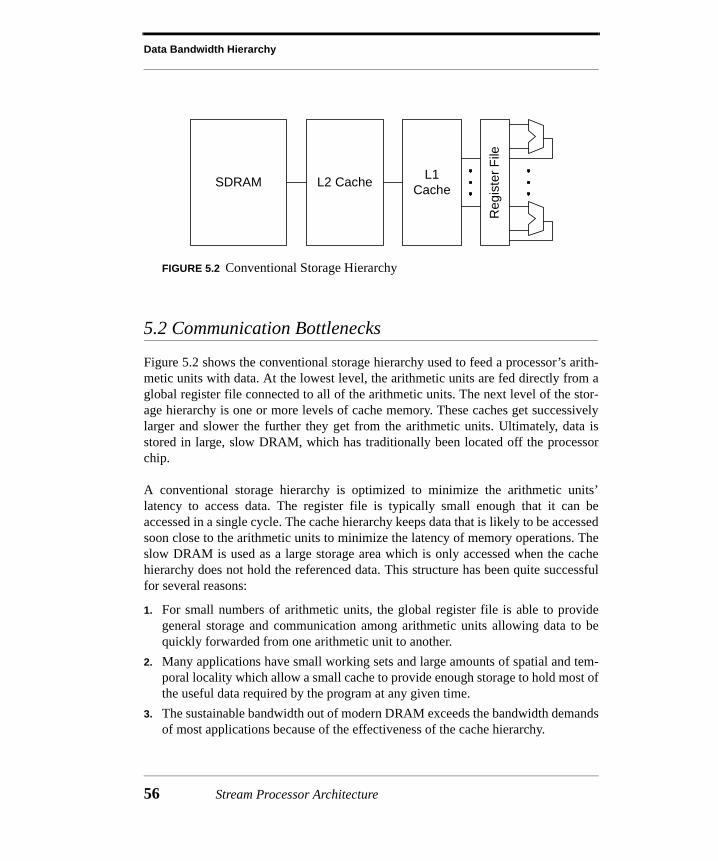
Data Bandwidth Hierarchy
5.2 Communication Bottlenecks
Figure 5.2 shows the conventional storage hierarchy used to feed a processor’s arith-metic units with data. At the lowest level, the arithmetic units are fed directly from aglobal register file connected to all of the arithmetic units. The next level of the stor-age hierarchy is one or more levels of cache memory. These caches get successivelylarger and slower the further they get from the arithmetic units. Ultimately, data isstored in large, slow DRAM, which has traditionally been located off the processorchip.
A conventional storage hierarchy is optimized to minimize the arithmetic units’latency to access data. The register file is typically small enough that it can beaccessed in a single cycle. The cache hierarchy keeps data that is likely to be accessedsoon close to the arithmetic units to minimize the latency of memory operations. Theslow DRAM is used as a large storage area which is only accessed when the cachehierarchy does not hold the referenced data. This structure has been quite successfulfor several reasons:
1. For small numbers of arithmetic units, the global register file is able to providegeneral storage and communication among arithmetic units allowing data to bequickly forwarded from one arithmetic unit to another.
2. Many applications have small working sets and large amounts of spatial and tem-poral locality which allow a small cache to provide enough storage to hold most ofthe useful data required by the program at any given time.
3. The sustainable bandwidth out of modern DRAM exceeds the bandwidth demandsof most applications because of the effectiveness of the cache hierarchy.
FIGURE 5.2 Conventional Storage Hierarchy
Reg
iste
r F
ile
L1Cache
L2 CacheSDRAM
56 Stream Processor Architecture

Communication Bottlenecks
Conventional storage hierarchies, however, are not well matched to the demands ofmedia processing applications. The structures within the conventional hierarchy areoptimized to minimize data access latency. The global register file is designed for fastcommunication among a small number of arithmetic units, the cache hierarchy isoptimized to minimize memory latency, and the DRAM is utilized to provide largeamounts of storage. Rather than low latency, media processing applications demandhigh data bandwidth to sustain large amounts of independent processing. They requirefar more arithmetic units to achieve their requisite computation rates, tolerate longermemory latencies, and demand high bandwidth from off-chip memory. These charac-teristics are incompatible with the conventional storage hierarchy and render it inef-fective in the following ways:
1. The large computation demands of media applications make a centralized globalregister file inefficient, if not infeasible, because of the massive bandwidthrequired by the tens to hundreds of arithmetic units accessing it.
2. Media applications have very large working sets (such as images) and have verylittle temporal or spatial locality, making caches ineffective. Additionally, theincreased number of arithmetic units create bandwidth demands higher than acache hierarchy could deliver.
3. Media applications have extremely high memory bandwidth demands becausethey operate on large amounts of raw data (such as video sequences) continuouslytransferred from an external source that must be buffered in memory.
All three elements of the storage hierarchy prevent the required data bandwidth frombeing supplied to the arithmetic units. To support numerous arithmetic units, a globalregister file must provide a large amount of storage and provide high data bandwidth.Technology constraints make such a register file costly. Furthermore, the cache hier-archy cannot provide enough bandwidth to support the additional arithmetic units.Caches are burdened by the fact that they are transparent to the programmer and com-piler. Since the program does not direct data movement within the hardware, thecache must dynamically transfer and store data which may or may not be used in thefuture. The hardware overhead required to manage this memory limits the effectivebandwidth that a cache can provide. Without sufficient bandwidth from the cachehierarchy, the arithmetic units will often sit idle waiting for data from the cache.Finally, when the DRAM is managed to minimize the latency of references that mustaccess it, the sustained bandwidth of the DRAM is lowered. The following sectionsfurther describe the communication bottlenecks of the global register file, cache hier-archy, and DRAM.
Data Bandwidth Hierarchy 57

Data Bandwidth Hierarchy
5.2.1 Register File Structure
Programmable processors have typically combined storage and communicationamong arithmetic units into a centralized global register file. These register files havebeen designed to supply the peak bandwidth required by the arithmetic units. Sincemost processors have few arithmetic units (typically less than 10), this register filedesign has provided the simplest and most general mechanism for communicatingdata among arithmetic units. However, current technology constraints make such cen-tralized register files costly and inefficient, even for supporting relatively small num-bers of arithmetic units. A centralized global register file used to interconnect fourarithmetic units would be approximately 0.2mm2 in a 0.18µm CMOS process. Toconnect 16 arithmetic units, a centralized register file would be around 6.4mm2. Infact, the size of a centralized register file grows as N3 for N arithmetic units. Similarly,the power dissipated by a centralized register file grows as N3 and the delay grows asN3/2 [RDK+00b].
A centralized register file cannot efficiently support tens to hundreds of arithmeticunits because of its cost, in terms of area, power, and delay. To support the large num-ber of arithmetic units demanded by media processing applications, the register filemust be partitioned to reduce its cost. Register file partitioning has been used effec-tively in architectures such as the Compaq Alpha 21264 microprocessor [Kes99] andthe Texas Instruments ’C6000 digital signal processors [TH97]. Partitioning enablesincreased bandwidth from the register file structure at reduced cost, allowing the reg-ister files to support larger numbers of arithmetic units efficiently. A partitioned regis-ter file can be incorporated into the conventional storage hierarchy; however,conventional caches cannot scale enough to supply data bandwidth for the tens tohundreds of arithmetic units demanded by media processing applications.
5.2.2 Cache Hierarchy
In order for a cache hierarchy to be effective, applications must exhibit large amountsof spatial and temporal locality. By keeping frequently accessed data closer to thearithmetic units, the latency to access that data is drastically reduced. Media process-ing applications do not exhibit much temporal locality, since they typically only refer-ence data once, process it, and never reference it again. Therefore, holding recentlyaccessed data close to the arithmetic units in a cache is useless. Media applicationsalso do not exhibit much spatial locality, as they tend to access data in strided pat-terns. For non-unit strides, this leads to many words of each cache line being unrefer-enced, especially if the stride is larger than the cache line size. This renders thecache’s ability to prefetch data located in the vicinity of referenced data useless, as
58 Stream Processor Architecture
Communication Bottlenecks
that prefetched data will not be accessed. Also, most media processing applicationshave extremely large working sets, which can easily exceed the capacity of a cacheand cause thrashing.
Media processing applications are far more sensitive to bandwidth than latency. So,even if caching were effective for these applications, a cache’s ability to reduce mem-ory latency will not necessarily improve performance. Increasing the sustainablememory bandwidth would be far more beneficial for these bandwidth intensive appli-cations. An effective cache can reduce the bandwidth demands on external DRAM.The cache prevents unnecessary off-chip memory references from occurring by hold-ing recently accessed data on the chip. However, an ineffective cache can actuallyincrease the bandwidth demands on the DRAM. A cache, by its very nature, specula-tively prefetches data on every memory access. If that data is never referenced, whichis the case in applications without spatial locality, then precious DRAM bandwidthwas wasted transferring that data. This is increasingly problematic as memory band-width becomes more scarce compared to compute resources [BGK97].
Furthermore, a cache is an inefficient way to stage data from memory. Address trans-lation is required on every reference, accesses are made with long memory addresses,some storage within the cache must be allocated to address tags, and conflicts mayevict previously fetched data that will be referenced in the future. Despite this over-head, caches reduce memory latency dynamically at run-time and allow hardwarecontrolled management of on-chip memory. In conventional processors, these bene-fits offset the inefficiencies of a cache. However, media processing applications havepredictable memory behavior which allows entire streams of data to be non-specula-tively prefetched long before they are needed. Therefore, it is more efficient to pro-vide sufficient registers to hide the latency of memory and to prefetch data directlyinto those registers rather than into a cache.
5.2.3 DRAM
Off-chip DRAM bandwidth is fundamentally limited by the pins on the chip, both interms of the number of available pins and the achievable bandwidth per pin. Conven-tional synchronous DRAM (SDRAM) chips currently deliver a peak transfer rate ofup to about 133Mb/s per data pin. The peak data bandwidth of off-chip DRAM is fur-ther related to the number of pins that the processor can allocate to such memory.Somewhat recent improvements in DRAM have increased that rate to about 266Mb/sper pin in Double Data Rate SDRAM (DDR SDRAM) and about 800Mb/s per pin inRambus Direct RDRAM (DRDRAM [Cri97]).
Data Bandwidth Hierarchy 59

Data Bandwidth Hierarchy
However, existing DRAM architectures cannot sustain these rates on random memoryaccesses. To maximize memory bandwidth, modern DRAM components allow pipe-lining of memory accesses, provide several independent memory banks, and cachethe most recently accessed row of each bank. While these features increase the peaksupplied memory bandwidth, they also make the performance of the DRAM highlydependent on the access pattern. Depending on the reference pattern, 14-97% of off-chip DRAM bandwidth can actually be utilized on continuous memory stream trans-fers [RDK+00a]. Therefore, to maximize DRAM bandwidth, DRAM accesses mustbe carefully managed to take advantage of the internal DRAM structure, rather thanattempting to minimize latency by satisfying references in order. Similarly, on-chipstorage and bandwidth must be organized and managed so as to minimize transfers tothis off-chip memory and thereby avoid wasting precious off-chip memory band-width.
5.3 Register Organization
The communication bottlenecks of modern VLSI together with the streaming natureof media processing applications motivate an explicitly managed bandwidth hierar-chy to effectively utilize tens to hundreds of arithmetic units for media processingtasks. A bandwidth hierarchy allows media processing applications to utilize commu-nication-limited technology efficiently. Temporary data is stored locally in the arith-metic clusters where it may be accessed frequently and quickly. Intermediate streamsare stored on-chip in the SRF where they can be recirculated between kernels withoutrequiring costly memory references. Finally, input, output, and global data is stored inexternal DRAM, since it is referenced infrequently and requires large amounts ofstorage space. Data is referenced far more frequently in the levels of the hierarchythat are closer to the arithmetic units. Therefore, each level of the hierarchy must pro-vide successively more bandwidth than the level below it. Media applications mapnaturally to such a bandwidth hierarchy, enabling them to utilize inexpensive, localbandwidth when possible, and only consume expensive, global data bandwidth whenabsolutely necessary.
As shown in Section 5.2, the register file, cache, and DRAM are all communicationbottlenecks in modern VLSI. As explained in Section 5.2.3, modern DRAM band-width is constrained by the peak bandwidth of the pins devoted to accessing thatDRAM. Therefore, the only thing that can be done to improve the sustained band-width of the DRAM is to manage the accesses to that DRAM in order to take advan-tage of its internal structure. Maximizing the sustained bandwidth of modern DRAM
60 Stream Processor Architecture

Register Organization
will be discussed in Chapter 6. Since caching is not an effective method of improvingmedia processing performance, the register file must be structured such that it canhide the latency of memory. This section will therefore focus on how modern VLSItechnology constrains register file organization.
The cost of a register file, in terms of area, power, and delay, is directly related to thenumber of registers in the file, R, and the number of ports that access the file, p. Asshown in [RDK+00b], the area of a register file is proportional to p2R, the power dis-sipation is also proportional to p2R, and the delay is proportional to pR1/2. For a cen-tralized register file, both p and R are proportional to the number of arithmetic units inthe processor, leading to area and power proportional to N3 and delay proportional toN3/2 for N arithmetic units [RDK+00b]. Such a register file clearly does not scale wellto support large numbers of arithmetic units.
Media processing applications require more registers per arithmetic unit than a gen-eral-purpose processor since a conventional cache hierarchy is ineffective. Theseadditional registers are used to hide the latency of memory directly within the registerfile structure. This makes it even more difficult to scale the register file to supportlarge numbers of arithmetic units. As shown previously, media processing applica-tions can easily be expressed in the stream programming model to expose the parallel-ism in their computations and the regularity of their communications. The large datastreams that must be transferred to/from memory and between kernels could easilyinterfere with each other within a cache, make inefficient use of cache lines, andexceed a cache’s capacity. However, these same data streams can efficiently be storedin a large register file, as their access is regular and predictable at compile time.Unfortunately, the combined effect of these additional registers and the large numberof arithmetic units needed by media processing applications further increases the costof the register file. A register file must, therefore, be partitioned in order to reduce itsarea, power, and delay to acceptable levels.
One efficient way to partition a register file is shown in Figure 5.3. A distributed reg-ister file (DRF) organization such as this can provide inexpensive data bandwidth to alarge number of arithmetic units. Each arithmetic unit has a small two-ported registerfile connected directly to each of its inputs. A single switch then routes data amongarithmetic units and register files, in contrast to the centralized register file structurecommonly used in practice which effectively contains this switch inside of every reg-ister. The DRF organization reduces the area of the register file for N arithmetic unitsto be proportional to N2, instead of N3. Similarly, the power and delay of such a struc-ture is reduced N2 and N, respectively, as opposed to N3 and N3/2 [RDK+00b].
Data Bandwidth Hierarchy 61
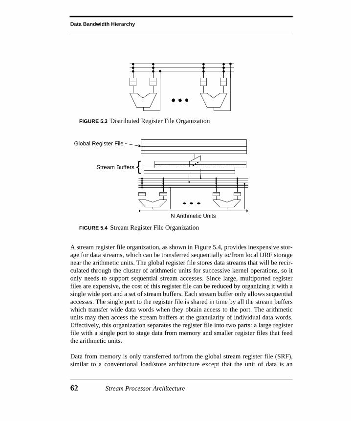
Data Bandwidth Hierarchy
A stream register file organization, as shown in Figure 5.4, provides inexpensive stor-age for data streams, which can be transferred sequentially to/from local DRF storagenear the arithmetic units. The global register file stores data streams that will be recir-culated through the cluster of arithmetic units for successive kernel operations, so itonly needs to support sequential stream accesses. Since large, multiported registerfiles are expensive, the cost of this register file can be reduced by organizing it with asingle wide port and a set of stream buffers. Each stream buffer only allows sequentialaccesses. The single port to the register file is shared in time by all the stream bufferswhich transfer wide data words when they obtain access to the port. The arithmeticunits may then access the stream buffers at the granularity of individual data words.Effectively, this organization separates the register file into two parts: a large registerfile with a single port to stage data from memory and smaller register files that feedthe arithmetic units.
Data from memory is only transferred to/from the global stream register file (SRF),similar to a conventional load/store architecture except that the unit of data is an
FIGURE 5.3 Distributed Register File Organization
FIGURE 5.4 Stream Register File Organization
Global Register File
Stream Buffers {
N Arithmetic Units
62 Stream Processor Architecture
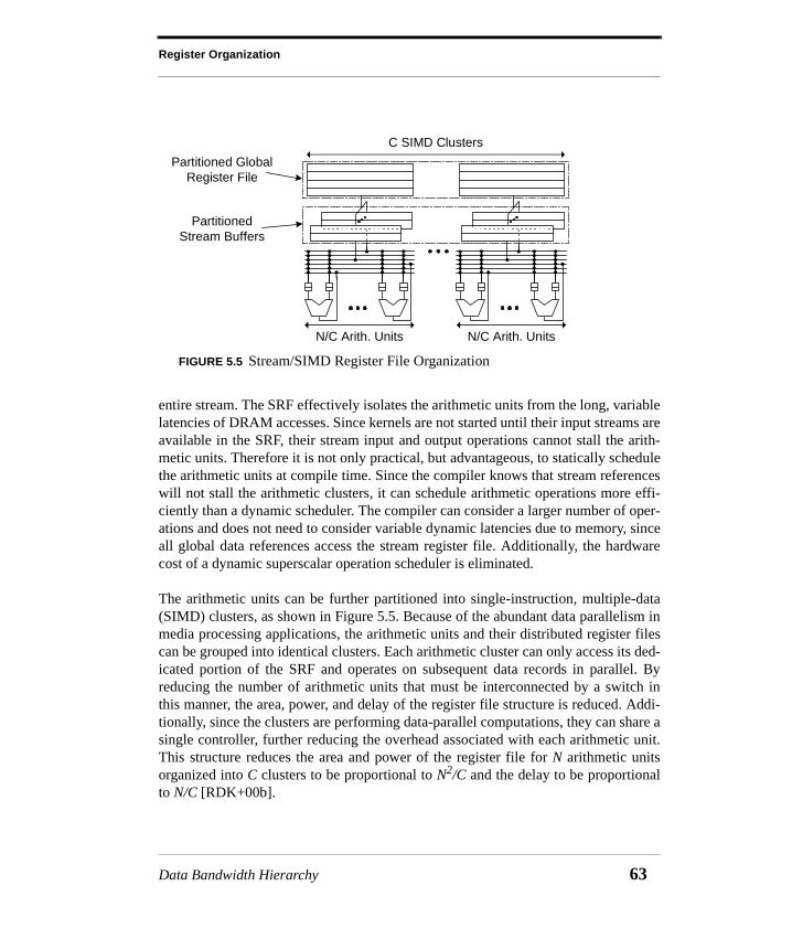
Register Organization
entire stream. The SRF effectively isolates the arithmetic units from the long, variablelatencies of DRAM accesses. Since kernels are not started until their input streams areavailable in the SRF, their stream input and output operations cannot stall the arith-metic units. Therefore it is not only practical, but advantageous, to statically schedulethe arithmetic units at compile time. Since the compiler knows that stream referenceswill not stall the arithmetic clusters, it can schedule arithmetic operations more effi-ciently than a dynamic scheduler. The compiler can consider a larger number of oper-ations and does not need to consider variable dynamic latencies due to memory, sinceall global data references access the stream register file. Additionally, the hardwarecost of a dynamic superscalar operation scheduler is eliminated.
The arithmetic units can be further partitioned into single-instruction, multiple-data(SIMD) clusters, as shown in Figure 5.5. Because of the abundant data parallelism inmedia processing applications, the arithmetic units and their distributed register filescan be grouped into identical clusters. Each arithmetic cluster can only access its ded-icated portion of the SRF and operates on subsequent data records in parallel. Byreducing the number of arithmetic units that must be interconnected by a switch inthis manner, the area, power, and delay of the register file structure is reduced. Addi-tionally, since the clusters are performing data-parallel computations, they can share asingle controller, further reducing the overhead associated with each arithmetic unit.This structure reduces the area and power of the register file for N arithmetic unitsorganized into C clusters to be proportional to N2/C and the delay to be proportionalto N/C [RDK+00b].
FIGURE 5.5 Stream/SIMD Register File Organization
C SIMD Clusters
N/C Arith. UnitsN/C Arith. Units
Partitioned GlobalRegister File
PartitionedStream Buffers
Data Bandwidth Hierarchy 63
Data Bandwidth Hierarchy
A partitioned register organization, including local distributed register files and a glo-bal stream register file divided into SIMD clusters, and external DRAM combine toform an efficient bandwidth hierarchy. A 32-bit wide single data rate SDRAM operat-ing at 125MHz yields a peak bandwidth of 500MB/s and a single Rambus channeloperating at 400MHz yields a peak bandwidth of 1.6GB/s. Therefore, by allocatingpins to four external banks of DRAM, modern DRAM can provide 2-6.4GB/s of peakdata bandwidth. A stream register file spanning most of the width of a 1cm2 chip pro-vides a peak bandwidth of 32-64GB/s, an order of magnitude higher than DRAM. Aneight cluster, distributed register file structure supporting 48 total arithmetic units canprovide a peak bandwidth in excess of 500GB/s, an order of magnitude higher than aglobal stream register file.
5.4 Evaluation
The bandwidth hierarchy described in the previous section is well-matched to modernVLSI technology, but to be useful, applications must be able to take advantage of it. Ifapplications perform only a single operation on each unique word referenced in mem-ory, then the bandwidth hierarchy would be rendered useless and the computation ratewould be entirely limited by memory bandwidth. Ideally, the ratio among memoryreferences, global data references, and local data references would exactly match thesupplied bandwidth of the three levels of the hierarchy. In practice, the applicationdemands lie somewhere between these two extremes.
This section will evaluate the efficiency of the bandwidth hierarchy. First, Section5.4.1 will show that kernels can make efficient use of local register files for temporarystorage to feed the arithmetic units and of an SRF to feed input streams to the arith-metic units and store output streams from the arithmetic units. Second, Section 5.4.2will show that when kernels are considered as part of an application, rather than inisolation, the SRF can be efficiently used to capture the locality of stream recircula-tion within media processing applications, thereby limiting the bandwidth demandson off-chip memory. Third, Section 5.4.3 will show that media processing applica-tions demand successively increasing amounts of bandwidth when they are mapped tothe three-tiered storage hierarchy described in this chapter. Fourth, Section 5.4.4 willshow that the hierarchical bandwidth scaling of the storage hierarchy is in fact whatenables these media processing applications to achieve 77-96% of the performancethat they would sustain given infinite instantaneous data bandwidth. Finally, Section5.4.5 will show the sustained performance and arithmetic utilization that the databandwidth hierarchy enables Imagine to achieve.
64 Stream Processor Architecture

Evaluation
5.4.1 Kernel Comparison
A comparison of kernel performance across programmable architectures shows theadvantages of the bandwidth hierarchy within a stream processor. Consider a simplemedia processing kernel, a Finite Impulse Response (FIR) filter. An FIR filter is a onedimensional convolution of a small kernel over a long data stream. The followingequation describes the operation (M is the number of coefficients in the filter):
(5.1)
Input values that do not exist on the boundaries of the computation are defined to be0. In this section, a 13-tap filter is used consisting of 16-bit fixed-point coefficientswith 15 bits of fraction and one sign bit, making the coefficients, k, lie in the range-1 ≤ k < 1. The input stream also consists of 16-bit fixed-point numbers with the out-put having the same precision as the input. For accuracy, the 32-bit products aresummed at 32-bit precision and then rounded and shifted to generate the final 16-bitresults. The input stream can be zero padded to simplify boundary cases, although thisis not necessary.
Figure 5.6 shows the C code for a simple implementation of such an FIR filter. Itassumes that there are extra zeros at the beginning and end of the input stream so thatbounds checking does not need to be performed. Also, the coefficient array isreversed to simplify the index calculations. All of the implementations of the FIR fil-ter presented in this section are functionally equivalent to this C code, except that theimplementations either do not require zero padding or only require it on one end ofthe input.
The number of global data references and the number of arithmetic operationsrequired by this kernel can be determined directly from the C code. Assuming an infi-
for (n=0; n<NUMOUTPUTS; n++){ sum = 0; // 32-bit accumulator for (i=0; i<13; i++) sum += k[i] * input[n+i]; // MAC for convolution output[n] = (sum + 0x4000) >> 15; // Round and shift to 16 bits}
FIGURE 5.6 C Code for a 13-tap, 16-bit Fixed-point, Real FIR Filter
y n( ) ki x n i–( )⋅
i 0=
M 1–
∑=
Data Bandwidth Hierarchy 65

Data Bandwidth Hierarchy
nite amount of register storage, each input would have to be loaded once, each outputwould have to be stored once, and the 13 coefficients would have to be loaded into theregister file once. This would lead to a total of slightly more than 4 bytes of memoryreferenced per output. For each output, 13 multiplies, 13 additions, and one shift arerequired (the C code performs one extra addition operation for simplicity). If the onlyregister file references made by the code were to support the minimum required trans-fers between memory and the register file and to support the input and outputs of thecomputations, this would lead to a total of 276 bytes referenced in the register file peroutput.
Table 5.1 shows the bandwidth demands of this FIR filter for a scalar digital signalprocessor (Texas Instruments TMS320C6203 [TH97]), a parallel-subword enhancedgeneral-purpose processor (Intel Pentium II MMX [PW96]), and a stream processor(Imagine). The ’C6 DSP has a similar architecture to the conventional architecturepresented at the beginning of this chapter. However, instead of a single centralizedregister file, the eight arithmetic units are split into two groups of four, each with itsown register file. The on-chip memory of the ’C6 can be configured either as cache oras addressable memory, with equivalent bandwidth in both organizations. The archi-tecture of the Pentium II is a very close approximation to the conventional storagestructure. The parallel-subword extensions (MMX [PW96]) allow SIMD operationsto be performed on data within the 64-bit floating-point registers. This improves per-formance and efficiency when performing the 16-bit and 32-bit calculations of theFIR filter. Imagine, described in Chapter 4, utilizes a data bandwidth hierarchy.
As can be seen in Table 5.1, all of the processors use more bandwidth than is strictlynecessary to perform the FIR filter. The DSP references 36 bytes of memory per out-put, rather than the 4 bytes that are necessary, because 16 coefficients and 18 inputsare loaded for every pair of outputs, leading to 32 bytes of additional memory traffic.For each pair of outputs, 16 coefficients and 18 inputs are loaded, instead of 13 coef-
DSP Parallel-subword Stream
Memory 36.0 49.9 ≤ 4.03
Global Register File 664.1 296.7 4.03
Local Register File N/A N/A 420.02
TABLE 5.1 Bytes Referenced per 16-bit FIR Filter Output (2048 Output, 13-tap filter)
66 Stream Processor Architecture

Evaluation
ficients and 14 inputs, because the filter procedure is unrolled such that the filterlength must be a multiple of eight. FIR filters with lengths that are not a multiple ofeight would achieve the same performance as if their length were the next multiple ofeight, so the code for a 16-tap filter was used with three of the taps being zero. Over664 bytes are referenced within the register file per output for this version of the code,as opposed to the 276 bytes that are strictly necessary, for the following reasons: theextra memory traffic also generates additional register accesses, the 32-bit registersare used to hold 16-bit values causing useless bytes to be accessed for 16-bit opera-tions, and addressing and loop counting operations require register usage.
The MMX version of the code suffers similar problems as the DSP in terms of mem-ory references. For every pair of outputs, 52 coefficients and 16 inputs are loaded.Since the inputs are packed into 64-bit words, four copies of the 13 filter coefficientsare required. Each copy is stored in four 64-bit words, aligned to start at a different16-bit boundary. Unlike the DSP version of the code, this version is optimized for a13-tap filter, so the additional coefficients are only needed to solve alignment issues.For each pair of outputs, 16 inputs are loaded, rather than 14, as the inputs are alsostored in 64-bit words. This leads to the additional 46 bytes of memory referencesover the required 4 bytes per output. The MMX version of the code, however, is veryefficient in its register usage, requiring only about 297 bytes of register accesses incomparison to the required 276. This is due to several factors: the Pentium allows oneoperand of many operations to come from memory and the 64-bit words are used toefficiently hold four 16-bit samples or two 32-bit accumulators. Otherwise, the MMXcode suffers from similar addressing and loop counting overhead.
The table clearly shows the benefits of the bandwidth hierarchy in the Imagine col-umn. Imagine avoids unnecessary memory traffic, separates global and local data, anddoes not require addressing calculations to access streams. Imagine makes very closeto the minimum required number of memory references (4.03 bytes). Each input isloaded once, each output is stored once, and 26 coefficients are loaded once for theentire filter (the 16-bit coefficients are packed into 32-bit words, so two differentlyaligned copies are required, as in the MMX code). In an application, the input to theFIR is likely to have been produced by a previous kernel and the output from the FIRis likely to be consumed by a subsequent kernel. Therefore, the table lists Imagine’smemory references as less than or equal to 4.03 bytes because, in practice, the input tothe FIR will already be in the SRF and the output will stay in the SRF. Imagine alsoonly references these same 4.03 bytes in the global register file. Once the coefficientsare moved into the arithmetic clusters, they are stored locally for the duration of thecomputation. Similarly, since there is enough register storage provided by the DRFstructure of the local register files, inputs do not need to be loaded repeatedly. There-
Data Bandwidth Hierarchy 67
Data Bandwidth Hierarchy
fore, only 4.03 bytes per output are referenced in the SRF. Imagine references 420bytes of local register storage per output, compared to the required 276 bytes, in orderto transfer data around from one register file to another within the DRF structure.Data must be transferred among register files in the DRF structure to facilitate soft-ware pipelining and to duplicate data that is needed by multiple functional units. Thislocal register bandwidth, however, is much cheaper to provide than global registerbandwidth, so these additional referenced bytes do not hurt performance.
Figure 5.7 shows the FIR filter kernel written in the stream programming model. Theinner loop from the C code implementation is completely unrolled to enable betterperformance when the outer loop is software pipelined. The 16-bit inputs are packedinto 32-bit words (the half2 data type consists of two 16-bit values packed into a sin-gle 32-bit word), so in each loop iteration, two inputs values are read per cluster andtwo output values are written per cluster. The code in the first page of the figure is theoverhead required to correctly compute the FIR on an eight cluster SIMD machine.At the top of each loop iteration, each cluster reads two new input values. Since theinputs are interleaved across the eight clusters, they are rotated (using thecommucperm instruction), and delayed for one loop iteration if necessary (using the?: operator and cluster_id() value), in order to provide each cluster with the previoustwelve inputs that will be needed to produce that cluster’s two outputs.
Since the setup code on the first page of the figure places the correct 14 inputs intoin01 through inAB, all eight clusters are able to compute their outputs in parallel. Thecode in the second page of the figure is the unrolled computations needed to computetwo outputs of the FIR filter. The muld operator takes two packed 16-bit inputs andmultiplies the high 16-bit values of each word to produce one 32-bit result and multi-plies the low 16-bit values of each word to produce another 32-bit result. The hi_looperator – which is a language construct, not a hardware instruction – places thesetwo 32-bit products into its two arguments. These products are then summed androunded to produce two output values, outC and outD. These 16-bit values are thenpacked into a single 32-bit word and output to the SRF.
Table 5.2 shows the performance and bandwidth usage of the three processors on theFIR filter. The results in the table are generated assuming that all three processorshave memory systems with infinite bandwidth that never cause the processors to stall.The number of operations that an architecture can perform per byte referenced in reg-ister files or memory can be calculated by dividing the sustained performance in thetable by the appropriate data bandwidth in the table. For example, Imagine is able toperform 6.7 operations per byte referenced in the global register file, whereas the 'C6and Pentium II are only able to perform 0.04 and 0.09 operations per byte, respec-
68 Stream Processor Architecture

Evaluation
tively. Therefore, to achieve a given level of performance, the bandwidth hierarchy ofImagine requires two orders of magnitude less global register file bandwidth. By off-loading the job of feeding the arithmetic units from the global register file to the localregister files, the bandwidth hierarchy is able to support a much larger number ofarithmetic units using a global register file with approximately the same peak band-width. Imagine achieves a similar number of operations per byte of local register filebandwidth (0.06) as the other architectures do per byte of global bandwidth. How-ever, since local register bandwidth is inexpensive in terms of area, power, and delay,far more arithmetic units can be supported. This allows Imagine to achieve over17GOPS on the FIR filter, while the ’C6 and Pentium II can only achieve about 1 and1.5GOPS, respectively. Even if the Pentium II’s clock speed is increased to 750MHzto account for technology differences, it would still only achieve about 2.5GOPS with0.09 operations per byte of global register bandwidth. Therefore, the bandwidth hier-archy of a stream processor efficiently scales data bandwidth that can be effectivelyutilized by media processing applications to achieve higher performance.
Table 5.2 also shows the utilization of the arithmetic units of each processor in theinner loop of the FIR filter kernel. The 'C6, which is optimized for such digital signalprocessing functions as the FIR filter, achieves 100% utilization of its eight arithmeticunits. This is possible because the types of arithmetic units are an exact match for thiskernel. The Pentium II is only able to achieve 94% utilization of its two arithmeticunits. Data dependencies prevent a few of the issue slots in the inner loop from being
DSP Parallel-subword Stream
Processor TMS320C6203 Pentium II MMX Imagine
Technology (µm) 0.15 0.25 0.15
Frequency (MHz) 300 450 500
Performance (GOPS) 1.01 1.47 17.57
Inner Loop ALU Utilization (%)
100 94 77
Local RF BW (GB/s) N/A N/A 273.25
Global RF BW (GB/s) 24.88 16.20 2.62
Memory BW (GB/s) 1.42 2.73 ≤ 2.62
TABLE 5.2 FIR Filter Performance and Bandwidth (2048 Output, 13-tap Filter)
Data Bandwidth Hierarchy 69

Data Bandwidth Hierarchy
kernel firfx13(istream<half2> data,istream<half2> krnl,ostream<half2> output)
{// Declare variableshalf2 k01, k23, k45, k67, k89, kAB, kC_; // Kernel for high outputhalf2 k_0, k12, k34, k56, k78, k9A, kBC; // Kernel for low outputhalf2 in01, in23, in45, in67, in89, inAB, inCD; // Input Datahalf2 com01, com23, com45, com67, com89, comAB; // Communicated datahalf2 dly01, dly23, dly45, dly67, dly89, dlyAB; // Delayed data;int p00, p11, p22, p33, p44, p55, p66, p77, p88, p99, pAA, pBB, pCC;int p01, p12, p23, p34, p45, p56, p67, p78, p89, p9A, pAB, pBC, pCD;int sum00, sum01, sum02;int sum10, sum11, sum12;int outC, outD;half2 outCD;
// Input kernel (1.15 fixed point numbers)krnl >> k01 >> k23 >> k45 >> k67 >> k89 >> kAB >> kC_;krnl >> k_0 >> k12 >> k34 >> k56 >> k78 >> k9A >> kBC;
// Initialized delayed data to 0dly01 = 0; dly23 = 0; dly45 = 0; dly67 = 0; dly89 = 0; dlyAB = 0;
// Mask to pack two 16-bit results into a 32-bit wordcc packcc = itocc(0xFFFF0000);
loop_stream(data) pipeline(1) { // Get next data elements (2 packed 16-bit values per 32-bit word) data >> inCD;
// Communicate data to other clusters comAB = commucperm(rotateRightBy1, inCD); com89 = commucperm(rotateRightBy2, inCD); com67 = commucperm(rotateRightBy3, inCD); com45 = commucperm(rotateRightBy4, inCD); com23 = commucperm(rotateRightBy5, inCD); com01 = commucperm(rotateRightBy6, inCD);
// Select between current and delayed data (for end clusters) inAB = (cluster_id() < 1) ? dlyAB : comAB; in89 = (cluster_id() < 2) ? dly89 : com89; in67 = (cluster_id() < 3) ? dly67 : com67; in45 = (cluster_id() < 4) ? dly45 : com45; in23 = (cluster_id() < 5) ? dly23 : com23; in01 = (cluster_id() < 6) ? dly01 : com01;
// Delay data for end clustersdlyAB = comAB; dly89 = com89; dly67 = com67;dly45 = com45; dly23 = com23; dly01 = com01;
FIGURE 5.7 KernelC Code for a 13-tap, 16-bit Fixed-point, Real FIR Filter
70 Stream Processor Architecture
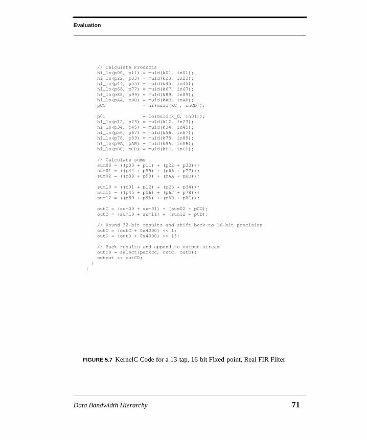
Evaluation
// Calculate Products hi_lo(p00, p11) = muld(k01, in01); hi_lo(p22, p33) = muld(k23, in23); hi_lo(p44, p55) = muld(k45, in45); hi_lo(p66, p77) = muld(k67, in67); hi_lo(p88, p99) = muld(k89, in89); hi_lo(pAA, pBB) = muld(kAB, inAB); pCC = hi(muld(kC_, inCD));
p01 = lo(muld(k_0, in01)); hi_lo(p12, p23) = muld(k12, in23); hi_lo(p34, p45) = muld(k34, in45); hi_lo(p56, p67) = muld(k56, in67); hi_lo(p78, p89) = muld(k78, in89); hi_lo(p9A, pAB) = muld(k9A, inAB); hi_lo(pBC, pCD) = muld(kBC, inCD);
// Calculate sums sum00 = ((p00 + p11) + (p22 + p33)); sum01 = ((p44 + p55) + (p66 + p77)); sum02 = ((p88 + p99) + (pAA + pBB));
sum10 = ((p01 + p12) + (p23 + p34)); sum11 = ((p45 + p56) + (p67 + p78)); sum12 = ((p89 + p9A) + (pAB + pBC));
outC = (sum00 + sum01) + (sum02 + pCC); outD = (sum10 + sum11) + (sum12 + pCD);
// Round 32-bit results and shift back to 16-bit precision outC = (outC + 0x4000) << 1; outD = (outD + 0x4000) >> 15;
// Pack results and append to output streamoutCD = select(packcc, outC, outD);output << outCD;
}}
FIGURE 5.7 KernelC Code for a 13-tap, 16-bit Fixed-point, Real FIR Filter
Data Bandwidth Hierarchy 71

Data Bandwidth Hierarchy
used. Finally, Imagine achieves 77% utilization of it’s 48 arithmetic units. The eightdividers go unused in this kernel, and the communication unit is 100% utilized, pre-venting further improvement. Even though the mix of arithmetic units in Imagine isnot as ideally suited to the FIR filter kernel as the mix of units in the 'C6, the band-width hierarchy still enables Imagine to keep over three-fourths of its computeresources busy.
The performance of the FIR filter kernel presented here does not show the actualeffects of memory latency and bandwidth. Table 5.2 shows the amount of memorybandwidth that would be needed in order to sustain the given computation rates. Thestructure of the memory system and the reference locality of the memory accessesdetermine how much of that bandwidth would actually need to be provided by exter-nal DRAM. The 'C6 and Pentium II would be able to satisfy many of their memoryreferences directly out of their on-chip caches. Depending on data placement, how-ever, conflicts may evict some reusable data. The 'C6 would be able to avoid theseevictions by configuring on-chip memory as addressable storage, rather than a cache.External DRAM must provide the bandwidth that is not provided by these on-chipmemories and caches. If the majority of the memory bandwidth demand is not satis-fied by on-chip resources, then these applications will become memory bound andtheir sustained computation rates will drop.
If the FIR filter was the only processing being performed on the data streams in Imag-ine, then all of the required memory bandwidth given in Table 5.2 would have tocome from external DRAM. However, when entire applications are considered, thebandwidth hierarchy of Imagine enables many of the memory references required bythe FIR filter kernel to be eliminated. Streams would be recirculated through the SRFfrom one kernel to the next, so the inputs and outputs of the FIR would not need to bestored in memory. Rather, the output of a previous kernel would be recirculatedthrough the SRF and input to the FIR, and the output of the FIR would be recirculatedthrough the SRF to another kernel. This recirculation of streams through the SRF dra-matically reduces the bandwidth demands on memory in Imagine.
5.4.2 Application Evaluation
The MPEG2 I-frame encoder, introduced in Section 4.1.2, efficiently utilizes thebandwidth hierarchy to minimize references to the SRF and off-chip memory. Figure5.8 shows how the MPEG2 I-Frame encoder maps to the three-tiered bandwidth hier-archy. The figure also shows the number of bytes that are referenced by the applica-tion at each level of the hierarchy. The seven computation kernels of the applicationexecute on the arithmetic clusters, as shown in the figure. During the execution of
72 Stream Processor Architecture

Evaluation
each kernel, the SRF is only referenced to read the kernel’s inputs and write the ker-nel’s outputs. For example, the color conversion kernel reads RGB pixels from itsinput stream, performs operations on local data, and writes luminance and chromi-nance pixels to its output streams. All intermediate data is stored in the local registerfiles within the clusters, resulting in 154.4MB of data being referenced within thoseregister files. As each pixel is converted by the color conversion kernel, for instance,all of the partial sums and products are stored within these local register files. Datastreams that are passed from kernel to kernel are stored within the SRF and do notneed to return to memory, as shown in the figure. This results in 4.8MB of data being
FIGURE 5.8 I-Frame Encoding from MPEG2 Encoder
ColorConversion
DCT
DCT
IDCT
IDCT
Run-LevelEncoding
VariableLengthCoding
Arithmetic ClustersStream Register FileMemory (or I/O)
InputImage
RGBPixels
LuminancePixels
TransformedLuminance
LuminanceReference
EncodedBitstream
RLE Stream
Bitstream
ReferenceChrominance
Image
ReferenceLuminance
Image
ChrominancePixels
TransformedChrominance
ChrominanceReference
Data Referenced: 835KB 4.8MB 154.4MB
MemoryBandwidth
SRFBandwidth
Data Bandwidth Hierarchy 73
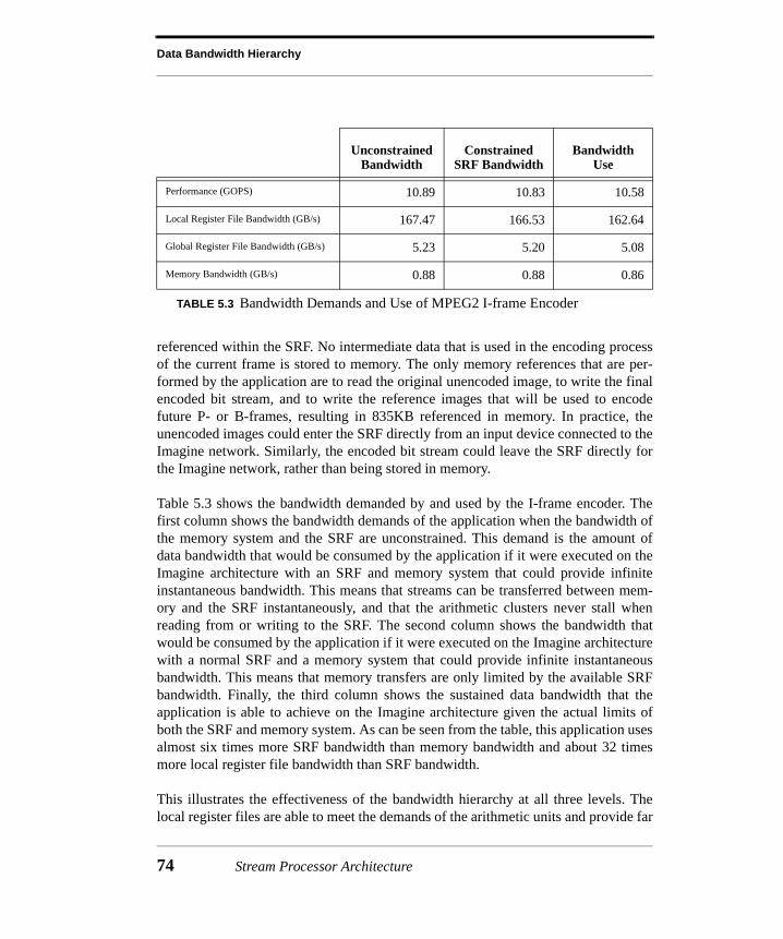
Data Bandwidth Hierarchy
referenced within the SRF. No intermediate data that is used in the encoding processof the current frame is stored to memory. The only memory references that are per-formed by the application are to read the original unencoded image, to write the finalencoded bit stream, and to write the reference images that will be used to encodefuture P- or B-frames, resulting in 835KB referenced in memory. In practice, theunencoded images could enter the SRF directly from an input device connected to theImagine network. Similarly, the encoded bit stream could leave the SRF directly forthe Imagine network, rather than being stored in memory.
Table 5.3 shows the bandwidth demanded by and used by the I-frame encoder. Thefirst column shows the bandwidth demands of the application when the bandwidth ofthe memory system and the SRF are unconstrained. This demand is the amount ofdata bandwidth that would be consumed by the application if it were executed on theImagine architecture with an SRF and memory system that could provide infiniteinstantaneous bandwidth. This means that streams can be transferred between mem-ory and the SRF instantaneously, and that the arithmetic clusters never stall whenreading from or writing to the SRF. The second column shows the bandwidth thatwould be consumed by the application if it were executed on the Imagine architecturewith a normal SRF and a memory system that could provide infinite instantaneousbandwidth. This means that memory transfers are only limited by the available SRFbandwidth. Finally, the third column shows the sustained data bandwidth that theapplication is able to achieve on the Imagine architecture given the actual limits ofboth the SRF and memory system. As can be seen from the table, this application usesalmost six times more SRF bandwidth than memory bandwidth and about 32 timesmore local register file bandwidth than SRF bandwidth.
This illustrates the effectiveness of the bandwidth hierarchy at all three levels. Thelocal register files are able to meet the demands of the arithmetic units and provide far
UnconstrainedBandwidth
Constrained SRF Bandwidth
BandwidthUse
Performance (GOPS) 10.89 10.83 10.58
Local Register File Bandwidth (GB/s) 167.47 166.53 162.64
Global Register File Bandwidth (GB/s) 5.23 5.20 5.08
Memory Bandwidth (GB/s) 0.88 0.88 0.86
TABLE 5.3 Bandwidth Demands and Use of MPEG2 I-frame Encoder
74 Stream Processor Architecture
Evaluation
more data bandwidth than would be available in traditional architectures. The SRF isonly utilized for stream storage between kernels and therefore only needs to sustainan order of magnitude less data bandwidth. Finally, the memory system holds globaldata and is referenced only when necessary, keeping the overall memory demands to aminimum.
The local register files effectively supply the arithmetic units with data. The arith-metic clusters demand about 167.5GB/s of data bandwidth to achieve 10.9GOPS ofcomputational throughput. In practice, the local register files actually provide about162.6GB/s of bandwidth. However, the slight decrease from the demand occursbecause of SRF and memory bandwidth limitations, not bandwidth limitations of thelocal register files. The SRF limits the sustainable performance slightly; the arith-metic clusters are idle for about 0.5% of the run-time because the SRF is unable tosustain bandwidth bursts above 32GB/s for extended periods of time. The table showsthat constraining the SRF bandwidth reduces the application’s performance to10.8GOPS. The arithmetic clusters are also idle for about 2.5% of the run-time wait-ing for memory transfers to complete, further reducing performance to about10.6GOPS.
The SRF is utilized for intermediate stream storage between kernels. This results in asustained demand over the entire application of about 5GB/s. The SRF is actuallyable to provide over 97% of this bandwidth. As previously mentioned, the drop inbandwidth from the demand occurs because of limited memory bandwidth andbecause the application has bursty SRF access patterns that sometimes exceed the32GB/s of average bandwidth the SRF can provide. The utilization of the SRF forstream recirculation keeps the memory bandwidth demands at a realizable level.
The application demands only 0.88GB/s of memory bandwidth to sustain 10.9GOPSof computation. This is a ratio of 49.5 operations per word of memory referenced. It isnot difficult for the Imagine memory system to sustain a significant fraction of thisdemand. In fact, it is able to achieve about 97% of this bandwidth, almost one half ofthe peak bandwidth of the Imagine memory system.
5.4.3 Application Bandwidth Demands
For a given arithmetic capacity, a stream processor can achieve a peak computationrate based on the available parallelism within the applications. This rate can be mea-sured by providing infinite instantaneous data bandwidth from the SRF and memorysystem. Table 5.4 shows the peak computation rate on the Imagine stream processor,with 48 arithmetic units organized into eight SIMD clusters and a 128KB SRF, for the
Data Bandwidth Hierarchy 75
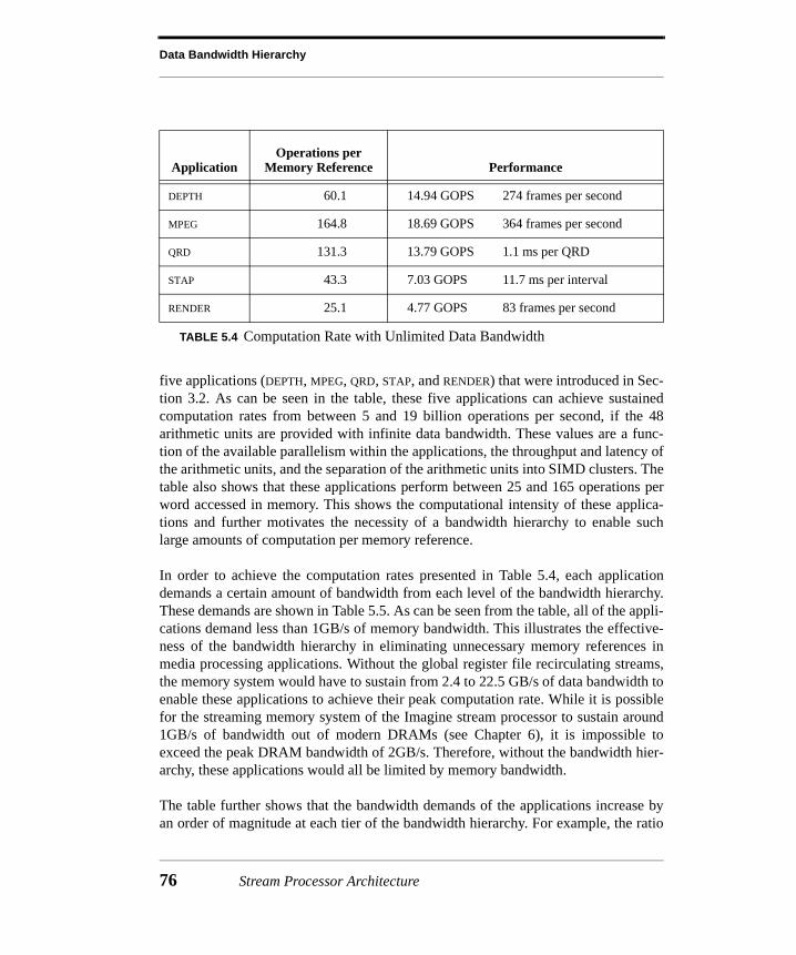
Data Bandwidth Hierarchy
five applications (DEPTH, MPEG, QRD, STAP, and RENDER) that were introduced in Sec-tion 3.2. As can be seen in the table, these five applications can achieve sustainedcomputation rates from between 5 and 19 billion operations per second, if the 48arithmetic units are provided with infinite data bandwidth. These values are a func-tion of the available parallelism within the applications, the throughput and latency ofthe arithmetic units, and the separation of the arithmetic units into SIMD clusters. Thetable also shows that these applications perform between 25 and 165 operations perword accessed in memory. This shows the computational intensity of these applica-tions and further motivates the necessity of a bandwidth hierarchy to enable suchlarge amounts of computation per memory reference.
In order to achieve the computation rates presented in Table 5.4, each applicationdemands a certain amount of bandwidth from each level of the bandwidth hierarchy.These demands are shown in Table 5.5. As can be seen from the table, all of the appli-cations demand less than 1GB/s of memory bandwidth. This illustrates the effective-ness of the bandwidth hierarchy in eliminating unnecessary memory references inmedia processing applications. Without the global register file recirculating streams,the memory system would have to sustain from 2.4 to 22.5 GB/s of data bandwidth toenable these applications to achieve their peak computation rate. While it is possiblefor the streaming memory system of the Imagine stream processor to sustain around1GB/s of bandwidth out of modern DRAMs (see Chapter 6), it is impossible toexceed the peak DRAM bandwidth of 2GB/s. Therefore, without the bandwidth hier-archy, these applications would all be limited by memory bandwidth.
The table further shows that the bandwidth demands of the applications increase byan order of magnitude at each tier of the bandwidth hierarchy. For example, the ratio
ApplicationOperations per
Memory Reference Performance
DEPTH 60.1 14.94 GOPS 274 frames per second
MPEG 164.8 18.69 GOPS 364 frames per second
QRD 131.3 13.79 GOPS 1.1 ms per QRD
STAP 43.3 7.03 GOPS 11.7 ms per interval
RENDER 25.1 4.77 GOPS 83 frames per second
TABLE 5.4 Computation Rate with Unlimited Data Bandwidth
76 Stream Processor Architecture

Evaluation
of memory references to global register file references to local register file referencesin the STAP application is roughly 1:11:276. Across all of the applications, thedemands on the SRF are 5 to 23 times higher than the demands on the memory sys-tem, and the demands on the local register files are 10 to 80 times higher than thedemands on the SRF. Therefore, the applications would clearly benefit from a band-width scaling that increases by roughly an order of magnitude at each level of thehierarchy.
Figure 5.9 shows the sensitivity of four of the applications to the size of the SRF. Thefigure shows the computation rate of each of the applications when the SRF andmemory system can provide infinite instantaneous bandwidth. As can be seen in thefigure, an SRF size of 20KW (80KB) is sufficient for the applications to achieve theirpeak rate for the problem sizes given in Section 3.2. MPEG benefits slightly frommore SRF space and is able to increase performance by 2% with a 36KW (144KB)SRF.
The performance of each application plateaus as the size of the SRF is increasedbecause the SRF becomes large enough to hold the applications’ working sets. As theSRF size is increased, so is the length of streams that can be processed by the applica-tions’ kernels. Each kernel has some overhead associated with starting and stoppingthe kernel. This overhead includes the time it takes the stream controller to initiate thekernel and set up its streams in the SRF, the code outside of kernel loops that is exe-cuted once each time a kernel is called, and the time spent priming and draining soft-ware pipelined loops within the kernels. However, all of these applications have anatural maximum useful stream length based on the input data. For instance, DEPTH
ApplicationMemory
Bandwidth (GB/s)Global Register
Bandwidth (GB/s)Local Register
Bandwidth (GB/s)
DEPTH 0.99 22.45 247.51
MPEG 0.45 2.40 197.51
QRD 0.42 4.23 298.72
STAP 0.65 6.94 179.07
RENDER 0.76 5.43 161.23
TABLE 5.5 Application Demands on a Stream Processor with Infinite Data Bandwidth
Data Bandwidth Hierarchy 77
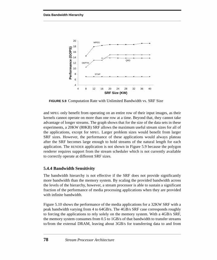
Data Bandwidth Hierarchy
and MPEG only benefit from operating on an entire row of their input images, as theirkernels cannot operate on more than one row at a time. Beyond that, they cannot takeadvantage of longer streams. The graph shows that for the size of the data sets in theseexperiments, a 20KW (80KB) SRF allows the maximum useful stream sizes for all ofthe applications, except for MPEG. Larger problem sizes would benefit from largerSRF sizes. However, the performance of these applications would always plateauafter the SRF becomes large enough to hold streams of the natural length for eachapplication. The RENDER application is not shown in Figure 5.9 because the polygonrenderer requires support from the stream scheduler which is not currently availableto correctly operate at different SRF sizes.
5.4.4 Bandwidth Sensitivity
The bandwidth hierarchy is not effective if the SRF does not provide significantlymore bandwidth than the memory system. By scaling the provided bandwidth acrossthe levels of the hierarchy, however, a stream processor is able to sustain a significantfraction of the performance of media processing applications when they are providedwith infinite bandwidth.
Figure 5.10 shows the performance of the media applications for a 32KW SRF with apeak bandwidth varying from 4 to 64GB/s. The 4GB/s SRF case corresponds roughlyto forcing the applications to rely solely on the memory system. With a 4GB/s SRF,the memory system consumes from 0.5 to 1GB/s of that bandwidth to transfer streamsto/from the external DRAM, leaving about 3GB/s for transferring data to and from
FIGURE 5.9 Computation Rate with Unlimited Bandwidth vs. SRF Size
4
6
8
10
12
14
16
18
20
4 8 12 16 20 24 28 32 36 40
SRF Size (KW)
Per
form
ance
(G
OP
S)
DEPTH
STAP
MPEG
QRD
78 Stream Processor Architecture

Evaluation
the arithmetic clusters. This is slightly more bandwidth than would be available fromthe 2GB/s memory system if the SRF were not part of the bandwidth hierarchy but islow enough to show the degradation in performance without an SRF that providessignificantly increased bandwidth over the memory system.
As can be seen in the figure, the sensitivity to the bandwidth of the SRF varies byapplication. DEPTH shows the most sensitivity, with a performance of over 5.6 timeshigher with a 64GB/s SRF compared to a 4GB/s SRF. This is not surprising, giventhat DEPTH is the application that demands the most SRF bandwidth at 22.45GB/s. Tosustain over 20GB/s across the entire application, the SRF must have a significantlyhigher peak bandwidth. The other applications show more modest improvements,ranging from 20% to 60%. These applications achieve most of their peak perfor-mance with an SRF that can provide 16GB/s, which is still eight times higher than thepeak memory bandwidth. Finally, the gap between the unlimited bandwidth perfor-mance and the actual achieved performance of all of the applications, except DEPTH,is due to memory bandwidth limitations. While DEPTH is able to overlap almost all ofits stream memory transfers with computation, dependencies prohibit the other appli-cations from hiding all of their memory transfers. Therefore, while the memory sys-tem is able to sustain a significant fraction of the average demand from theseapplications, it is not always able to provide the applications with their peak band-width demands.
5.4.5 Arithmetic Unit Utilization
Table 5.6 shows the utilization of the arithmetic units on Imagine and the resultingapplication performance. The various applications are able to utilize the arithmeticunits between 18% and 61%. This is lower than the 77% utilization that is achieved in
Application Arithmetic Unit Utilization (%) Performance (GOPS)
DEPTH 33.4 13.09
MPEG 36.8 17.88
QRD 60.7 12.49
STAP 26.6 5.47
RENDER 17.9 3.95
TABLE 5.6 Application Arithmetic Utilization and Performance on Imagine
Data Bandwidth Hierarchy 79

Data Bandwidth Hierarchy
FIGURE 5.10 Sustained Performance vs. Bandwidth of a 32KW SRF
QRD
12.49 12.49 12.4812.46
10.45
8
10
12
14
16
0 10 20 30 40 50 60 70
Peak SRF Bandwidth (GB/s)
Unlimited Bandwidth Performance (13.79 GFLOPS)
Per
form
ance
(G
FL
OP
S)
DEPTH
8.52
13.09
14.46
4.86
2.582
4
6
8
10
12
14
16
0 10 20 30 40 50 60 70
Peak SRF Bandwidth (GB/s)
Per
form
ance
(G
OP
S) Unlimited Bandwidth Performance (14.94 GOPS)
RENDER
3.89 3.95 3.973.48
2.65
0
1
2
3
4
5
6
0 10 20 30 40 50 60 70
Peak SRF Bandwidth (GB/s)
Unlimited Bandwidth Performance (4.77 GOPS)
Per
form
ance
(G
OP
S)
80 Stream Processor Architecture
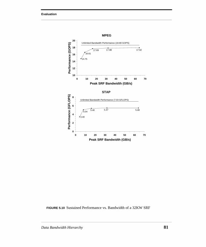
Evaluation
FIGURE 5.10 Sustained Performance vs. Bandwidth of a 32KW SRF
MPEG
17.69 17.88 17.92
16.61
14.75
10
12
14
16
18
20
0 10 20 30 40 50 60 70
Peak SRF Bandwidth (GB/s)
Per
form
ance
(G
OP
S) Unlimited Bandwidth Performance (18.69 GOPS)
STAP
5.40 5.47 5.485.04
3.40
0
2
4
6
8
0 10 20 30 40 50 60 70
Peak SRF Bandwidth (GB/s)
Unlimited Bandwidth Performance (7.03 GFLOPS)
Per
form
ance
(G
FL
OP
S)
Data Bandwidth Hierarchy 81
Data Bandwidth Hierarchy
the inner loop of the FIR filter kernel. During the execution of an application, thearithmetic units are left idle when stalled waiting for data from memory of the SRF,and there is far less computation outside of the inner loops of kernels. These factorsgreatly decrease the achievable arithmetic utilization of entire applications. However,because the data bandwidth hierarchy enables Imagine to support 48 arithmetic unitswith very high utilization during the inner loops of kernels, applications are still ableto achieve from 4 to 18GOPS of sustained computation.
5.5 Summary
Media processing applications benefit from a bandwidth scaling across multiple lev-els of the storage hierarchy to bridge the gap from modern DRAM bandwidth to thedata bandwidth required by the arithmetic units. Without this bandwidth scaling,media applications are memory bandwidth limited, which severely reduces the num-ber of arithmetic units that can be utilized efficiently. A three-tiered bandwidth hierar-chy, including distributed local register files, a global stream register file, and externalDRAM, can effectively meet the needs of these applications by scaling the bandwidthby over an order of magnitude at each level.
The bandwidth hierarchy enables media processing applications to utilize bandwidthefficiently. Kernels make efficient use of local register files for temporary storage tosupply the arithmetic units with data and of an SRF to supply input streams to thearithmetic units and store output streams from the arithmetic units. When kernels areconsidered as part of an application, rather than in isolation, the SRF can be effi-ciently used to capture the locality of stream recirculation within media processingapplications, thereby limiting the bandwidth demands on off-chip memory. Whenmapped to the three-tiered storage hierarchy described in this chapter, media process-ing applications demand successively increasing amounts of bandwidth. By matchingthese demands, the bandwidth scaling of the storage hierarchy enables these mediaprocessing applications to achieve 4-18GOPS, which is 77-96% of the performancethat they would sustain given infinite instantaneous data bandwidth.
82 Stream Processor Architecture

CHAPTER 6 Memory Access Scheduling
A streaming memory system, which forms the base of a stream processor’s data band-width hierarchy, transfers entire streams of data, rather than individual words. Sus-tained memory bandwidth directly contributes to the overall performance of a streamprocessor, so a streaming memory system is optimized for memory bandwidth, ratherthan memory latency. To maximize bandwidth, the memory system must take advan-tage of the characteristics of modern DRAM. The bandwidth and latency of a mem-ory system are strongly dependent on the manner in which accesses interact with the“3-D” structure of banks, rows, and columns characteristic of contemporary DRAMchips. Modern DRAM components allow memory accesses to be pipelined, provideseveral independent memory banks, and cache the most recently accessed row of eachbank. These features increase the peak performance of the DRAM, but also make thesustained performance highly dependent on the access pattern. There is nearly anorder of magnitude difference in bandwidth between successive references to differ-ent columns within a row and different rows within a bank. Memory access schedul-ing improves the performance of a memory system by reordering memory referencesto exploit locality within the 3-D memory structure. This chapter will discuss theorganization of modern DRAM, the architecture of a memory access scheduler, andtheir impact on sustained memory bandwidth for media processing.
Memory Access Scheduling 83

Memory Access Scheduling
6.1 Overview
As discussed previously, media applications require up to 300GB/s of data bandwidthto utilize 48 arithmetic units. An effective bandwidth hierarchy can bridge the gapbetween modern DRAM bandwidth and the bandwidth required by the arithmeticunits, which is over two orders of magnitude. However, for such a hierarchy to besuccessful, the memory system must be able to sustain a significant fraction of thepeak DRAM bandwidth. Chapter 5 showed that the five representative media process-ing applications demand from 0.4 to 1.0GB/s of memory bandwidth to achieve theirpeak computation rates. On the Imagine stream processor, this corresponds to 20-50%of the peak DRAM bandwidth. This can be achieved with a streaming memory sys-tem which employs memory access scheduling to take advantage of the locality andconcurrency of modern DRAM.
6.1.1 Stream Memory Transfers
A streaming memory system transfers streams of data between the processor andexternal DRAM, rather than individual words or cache lines as in a conventionalmemory system. A data stream is a sequence of records, where each record consists ofone or more words. Records represent media data, such as an audio sample, a com-plex frequency value, or a triangle vertex. The words that compose an individualrecord are stored contiguously in memory, but a stream may consist of records scat-tered throughout the memory space. The starting addresses of the records that com-pose a particular data stream can be calculated using a constant stride, bit-reversedarithmetic, or an index stream. The streaming memory system of the Imagine mediaprocessor was described in Section 4.2.4.
Since entire streams of data are transferred by the memory system, the latency of anyindividual reference is not important. Rather, the bandwidth of the transfer is whataffects performance. For example, consider the execution of the MPEG2 I-frameencoder on Imagine. Figure 6.1 shows the kernel operations and memory streamtransfers for a portion of the application’s execution. The figure shows parts of theprocessing of three batches of macroblocks. The left column shows kernel executionon the arithmetic clusters and the two columns on the right show stream memorytransfers. The load from memory of the macroblocks for batch i-1 occurs prior tocycle 6000, so is not shown. First the color conversion kernel is executed to convertthe original macroblocks into luminance and chrominance streams. Then the DCT,run-level encoding, and inverse DCT execute. The run-level encoded blocks arestored to memory after they are encoded. The kernel labelled “reference” in the figuresimply reorganizes data from the IDCT kernels to be in the proper format for use in P-
84 Stream Processor Architecture
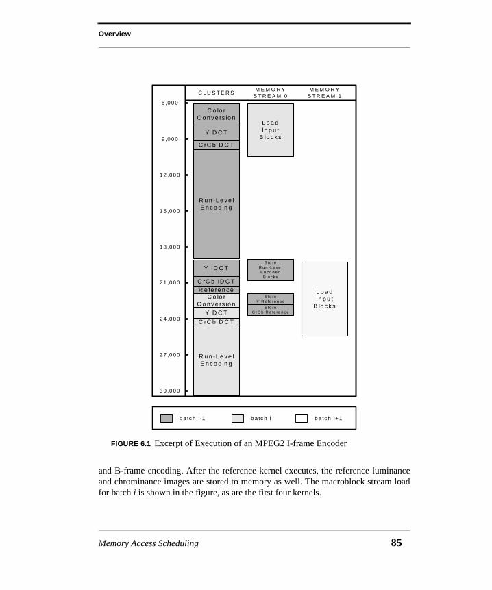
Overview
and B-frame encoding. After the reference kernel executes, the reference luminanceand chrominance images are stored to memory as well. The macroblock stream loadfor batch i is shown in the figure, as are the first four kernels.
FIGURE 6.1 Excerpt of Execution of an MPEG2 I-frame Encoder
6 ,0 00
9 ,0 00
1 2 ,0 00
1 5 ,0 00
1 8 ,0 00
2 1 ,0 00
2 4 ,0 00
2 7 ,0 00
3 0 ,0 00
C L U S T E R SM E M O R Y
S T R E A M 0M E M O R Y
S T R E A M 1
C o lo rC o n v e rs io n
L o a dIn p u t
B lo c k s
b a tc h i-1 b a tc h i b a tc h i+ 1
Y D C T
C rC b D C T
R u n -L e v e lE n c o d in g
S to reR u n -L e ve lE n co d e d
B lo c k s
Y ID C T
L o a dIn p u t
B lo c k s
C rC b ID C TR e fe re n c e
S to reY R e fe re n c e
C o lo rC o n v e rs io n
S to reC rC b R e fe re n c eY D C T
C rC b D C T
R u n -L e v e lE n c o d in g
Memory Access Scheduling 85
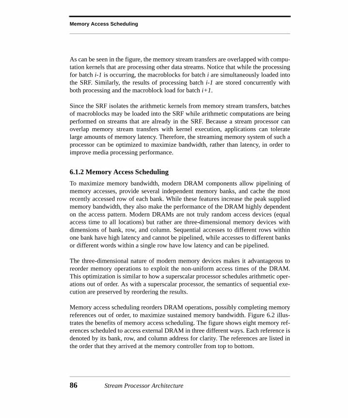
Memory Access Scheduling
As can be seen in the figure, the memory stream transfers are overlapped with compu-tation kernels that are processing other data streams. Notice that while the processingfor batch i-1 is occurring, the macroblocks for batch i are simultaneously loaded intothe SRF. Similarly, the results of processing batch i-1 are stored concurrently withboth processing and the macroblock load for batch i+1.
Since the SRF isolates the arithmetic kernels from memory stream transfers, batchesof macroblocks may be loaded into the SRF while arithmetic computations are beingperformed on streams that are already in the SRF. Because a stream processor canoverlap memory stream transfers with kernel execution, applications can toleratelarge amounts of memory latency. Therefore, the streaming memory system of such aprocessor can be optimized to maximize bandwidth, rather than latency, in order toimprove media processing performance.
6.1.2 Memory Access Scheduling
To maximize memory bandwidth, modern DRAM components allow pipelining ofmemory accesses, provide several independent memory banks, and cache the mostrecently accessed row of each bank. While these features increase the peak suppliedmemory bandwidth, they also make the performance of the DRAM highly dependenton the access pattern. Modern DRAMs are not truly random access devices (equalaccess time to all locations) but rather are three-dimensional memory devices withdimensions of bank, row, and column. Sequential accesses to different rows withinone bank have high latency and cannot be pipelined, while accesses to different banksor different words within a single row have low latency and can be pipelined.
The three-dimensional nature of modern memory devices makes it advantageous toreorder memory operations to exploit the non-uniform access times of the DRAM.This optimization is similar to how a superscalar processor schedules arithmetic oper-ations out of order. As with a superscalar processor, the semantics of sequential exe-cution are preserved by reordering the results.
Memory access scheduling reorders DRAM operations, possibly completing memoryreferences out of order, to maximize sustained memory bandwidth. Figure 6.2 illus-trates the benefits of memory access scheduling. The figure shows eight memory ref-erences scheduled to access external DRAM in three different ways. Each reference isdenoted by its bank, row, and column address for clarity. The references are listed inthe order that they arrived at the memory controller from top to bottom.
86 Stream Processor Architecture
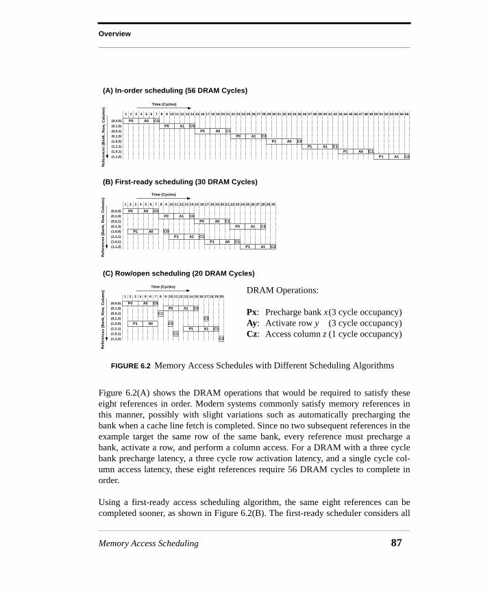
Overview
Figure 6.2(A) shows the DRAM operations that would be required to satisfy theseeight references in order. Modern systems commonly satisfy memory references inthis manner, possibly with slight variations such as automatically precharging thebank when a cache line fetch is completed. Since no two subsequent references in theexample target the same row of the same bank, every reference must precharge abank, activate a row, and perform a column access. For a DRAM with a three cyclebank precharge latency, a three cycle row activation latency, and a single cycle col-umn access latency, these eight references require 56 DRAM cycles to complete inorder.
Using a first-ready access scheduling algorithm, the same eight references can becompleted sooner, as shown in Figure 6.2(B). The first-ready scheduler considers all
FIGURE 6.2 Memory Access Schedules with Different Scheduling Algorithms
DRAM Operations:
Px: Precharge bank x(3 cycle occupancy)Ay: Activate row y (3 cycle occupancy)Cz: Access column z (1 cycle occupancy)
(A) In-order scheduling (56 DRAM Cycles)
(C) Row/open scheduling (20 DRAM Cycles)
(B) First-ready scheduling (30 DRAM Cycles)
11
(0,0,0)
(1,1,2)
(1,0,1)(1,1,1)
(1,0,0)
(0,1,3)(0,0,1)
(0,1,0)P0 A0 C0
292827262524232221191817161514131210987654321 20 39383736353433323130 4443424140
P0 A1 C0P0 A0 C1
P0 A1 C3P1 A0 C0
P1 A1 C1P1 A0 C1
P1 A1 C2
4948474645 50 565554535251
Time (Cycles)R
efer
ence
s (B
ank,
Ro
w, C
olu
mn
)
11
(0,0,0)
(1,1,2)(1,0,1)
(1,1,1)
(1,0,0)(0,1,3)
(0,0,1)
(0,1,0)P0 A0 C0
292827262524232221191817161514131210987654321 20 30
P0 A1 C0P0 A0 C1
P0 A1 C3
Time (Cycles)
Ref
eren
ces
(Ban
k, R
ow
, Co
lum
n)
P1 A0 C0P1 A1 C1
P1 A0 C1P1 A1 C2
11
(0,0,0)
(1,1,2)
(1,0,1)(1,1,1)
(1,0,0)(0,1,3)
(0,0,1)(0,1,0)
P0 A0 C0
191817161514131210987654321
P1 A0
C1P0
C0P1 A1
C1
A1 C0
C3
C1
C2
Ref
eren
ces
(Ban
k, R
ow
, Co
lum
n)
Time (Cycles)
20
Memory Access Scheduling 87

Memory Access Scheduling
pending references and schedules a DRAM operation for the oldest pending referencethat does not violate the timing and resource constraints of the DRAM. The mostobvious benefit of this scheduling algorithm over the in-order scheduler is thataccesses to other banks can be made while waiting for a precharge or an activate oper-ation to complete for the oldest pending reference. This relaxes the serialization of thein-order scheduler and allows multiple references to progress in parallel. In thisexample, the first-ready scheduler is able to exploit the bank parallelism in the refer-ence stream. The accesses for the references that target bank 1 can mostly be over-lapped with accesses for the references that target bank 0. The first-ready scheduler isable to complete the eight references in only 30 cycles. It is not always the case thatfirst-ready scheduling exploits all of the available bank parallelism and none of therow locality. If the same eight references had arrived in a different order, a first-readyscheduler would be able to exploit varying degrees of each.
More sophisticated scheduling algorithms can maximize DRAM bandwidth byexploiting more of the bank parallelism and row locality found in the pending mem-ory references. Figure 6.2(C) shows the DRAM accesses performed by a row/openscheduler, which will be explained later in the chapter. As can be seen in the figure, arow/open scheduler completes the eight references in only 20 DRAM cycles. Thisscheduler is able to exploit both the bank parallelism and row locality of the referencestream by overlapping accesses to banks 0 and 1 and by performing all of the columnaccesses to each row that is activated before precharging the bank for subsequent rowactivations.
6.2 Modern DRAM
The previous example illustrates that the order in which DRAM accesses are sched-uled can have a dramatic impact on memory throughput and latency. To maximizememory bandwidth, modern DRAM components allow pipelining of memoryaccesses, provide several independent memory banks, and cache the most recentlyaccessed row of each bank. While these features increase the peak supplied memorybandwidth, they also make the performance of the DRAM highly dependent on theaccess pattern. Therefore, a memory controller must take advantage of the character-istics of modern DRAM to improve performance.
Figure 6.3 shows the internal organization of modern DRAMs. These DRAMs arethree-dimensional memories with the dimensions of bank, row, and column. Eachbank operates independently of the other banks and contains an array of memory cells
88 Stream Processor Architecture

Modern DRAM
that are accessed an entire row at a time. When a row of this memory array isaccessed (row activation), the entire row of the memory array is transferred into thebank’s row buffer. The row buffer serves as a cache to reduce the latency of subse-quent accesses to that row. While a row is active in the row buffer, any number ofreads or writes (column accesses) may be performed, typically with a throughput ofone per cycle. After completing the available column accesses, the cached row mustbe written back to the memory array by an explicit operation (bank precharge), whichprepares the bank for a subsequent row activation. An overview of several differentmodern DRAM types and organizations, along with a performance comparison for in-order access, can be found in [CJDM99].
For example, the 128Mb NEC µPD45128163 [NEC98], a typical SDRAM, includesfour internal memory banks, each composed of 4096 rows and 512 columns. ThisSDRAM may be operated at 125MHz, with a precharge latency of 3 cycles (24ns) anda row access latency of 3 cycles (24ns). Pipelined column accesses that transfer 16bits may issue at the rate of one per cycle (8ns), yielding a peak transfer rate of250MB/s. However, it is difficult to achieve this rate on non-sequential access pat-terns for several reasons. A bank cannot be accessed during its precharge/activatelatency, a single cycle of high impedance is required on the data pins when switchingbetween read and write column accesses, and a single set of address lines is shared byall DRAM operations (bank precharge, row activation, and column access). The
FIGURE 6.3 Modern DRAM Organization
Bank N
Bank 1
Sense Amplifiers(Row Buffer)
Column Decoder
Row
Dec
oder
Data
Address
MemoryArray
(Bank 0)
Memory Access Scheduling 89

Memory Access Scheduling
amount of bank parallelism that is exploited and the number of column accesses thatare made per row access dictate the sustainable memory bandwidth out of such aDRAM.
A memory controller must generate a schedule that conforms to the timing andresource constraints of these modern DRAMs. Figure 6.4 illustrates these constraintsfor the NEC SDRAM with a simplified bank state diagram and a table of operationresource utilization. Each DRAM operation makes different demands on the threeDRAM resources (the internal banks, a single set of address lines, and a single set ofdata lines). The memory controller must ensure that the required resources are avail-able for each DRAM operation it issues.
Each DRAM bank has two stable states, IDLE and ACTIVE, as shown in Figure 6.4(A).In the IDLE state, the DRAM is precharged and ready for a row access. It will remainin this state until a row activation operation is issued to the bank. To issue a row acti-vation, the address lines must be used to select the bank and the row being activated,as shown in Figure 6.4(B). Row activation requires 3 cycles, during which no otheroperations may be issued to that bank, as indicated by the utilization of the bankresource for the duration of the operation. During that time, however, operations maybe issued to other banks of the DRAM. Once the DRAM’s row activation latency has
FIGURE 6.4 Internal DRAM Bank State Diagram and Resource Utilization
IDLE ACTIVE
Bank Precharge
Row Activation
Column Access
AddressBank
Data
Cycle 1 2 3
Precharge:
Activate:
Read:
Write:
4
AddressBank
Data
AddressBank
Data
AddressBank
Data
(A) Simplified bank state diagram (B) Operation resource utilization
90 Stream Processor Architecture
Modern DRAM
passed, the bank enters the ACTIVE state, during which the contents of the selectedrow are held in the bank’s row buffer. Any number of pipelined column accesses maybe performed while the bank is in the ACTIVE state. To issue either a read or write col-umn access, the address lines are required to indicate the bank and the column of theactive row in that bank. A write column access requires the data to be transferred tothe DRAM at the time of issue, whereas a read column access returns the requesteddata three cycles later. Additional timing constraints not shown in Figure 6.4, such asa required cycle of high impedance between reads and writes, may further restrict theuse of the data pins.
The bank will remain in the ACTIVE state until a precharge operation is issued toreturn it to the IDLE state. The precharge operation requires the use of the address linesto indicate the bank which is to be precharged. Like row activation, the prechargeoperation utilizes the bank resource for 3 cycles, during which no new operations maybe issued to that bank. Again, operations may be issued to other banks during thistime. After the DRAM’s precharge latency, the bank is returned to the IDLE state andis ready for a new row activation operation. Frequently, there are also timing con-straints that govern the minimum latency between a column access and a subsequentprecharge operation. DRAMs typically also support column accesses with automaticprecharge, which implicitly precharges the DRAM bank as soon as possible after thecolumn access.
The address and data resources are usually shared among the banks, thereby serializ-ing access to the internal banks.While the state machines for the individual banks areindependent, only a single bank can perform a transition requiring a particular sharedresource each cycle. For many DRAMs, the bank, row, and column addresses share asingle set of pins. Hence, the scheduler must arbitrate between precharge, row, andcolumn operations that all need to use this single resource. Other DRAMs, such asDirect Rambus DRAMs (DRDRAMs) [Cri97], provide separate row and columnaddress lines (each with their own associated bank address) so that column and rowaccesses can be initiated simultaneously. To approach the peak data rate with serial-ized resources, there must be enough column accesses to each row to hide the pre-charge/activate latencies of other banks. Whether or not this can be achieved isdependent on the data reference patterns and the order in which the DRAM isaccessed to satisfy those references. The need to hide the precharge/activate latencyof the banks in order to sustain high bandwidth cannot be eliminated by any DRAMarchitecture without reducing the precharge/activate latency, which would likelycome at the cost of decreased bandwidth or capacity, both of which are undesirable.
Memory Access Scheduling 91
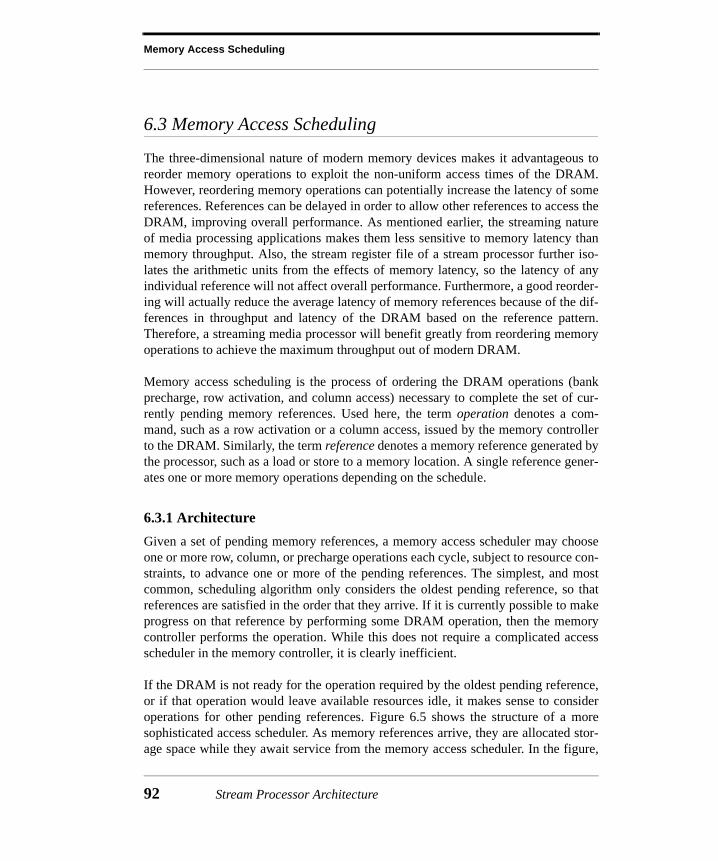
Memory Access Scheduling
6.3 Memory Access Scheduling
The three-dimensional nature of modern memory devices makes it advantageous toreorder memory operations to exploit the non-uniform access times of the DRAM.However, reordering memory operations can potentially increase the latency of somereferences. References can be delayed in order to allow other references to access theDRAM, improving overall performance. As mentioned earlier, the streaming natureof media processing applications makes them less sensitive to memory latency thanmemory throughput. Also, the stream register file of a stream processor further iso-lates the arithmetic units from the effects of memory latency, so the latency of anyindividual reference will not affect overall performance. Furthermore, a good reorder-ing will actually reduce the average latency of memory references because of the dif-ferences in throughput and latency of the DRAM based on the reference pattern.Therefore, a streaming media processor will benefit greatly from reordering memoryoperations to achieve the maximum throughput out of modern DRAM.
Memory access scheduling is the process of ordering the DRAM operations (bankprecharge, row activation, and column access) necessary to complete the set of cur-rently pending memory references. Used here, the term operation denotes a com-mand, such as a row activation or a column access, issued by the memory controllerto the DRAM. Similarly, the term reference denotes a memory reference generated bythe processor, such as a load or store to a memory location. A single reference gener-ates one or more memory operations depending on the schedule.
6.3.1 Architecture
Given a set of pending memory references, a memory access scheduler may chooseone or more row, column, or precharge operations each cycle, subject to resource con-straints, to advance one or more of the pending references. The simplest, and mostcommon, scheduling algorithm only considers the oldest pending reference, so thatreferences are satisfied in the order that they arrive. If it is currently possible to makeprogress on that reference by performing some DRAM operation, then the memorycontroller performs the operation. While this does not require a complicated accessscheduler in the memory controller, it is clearly inefficient.
If the DRAM is not ready for the operation required by the oldest pending reference,or if that operation would leave available resources idle, it makes sense to consideroperations for other pending references. Figure 6.5 shows the structure of a moresophisticated access scheduler. As memory references arrive, they are allocated stor-age space while they await service from the memory access scheduler. In the figure,
92 Stream Processor Architecture
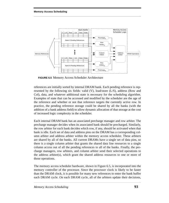
Memory Access Scheduling
references are initially sorted by internal DRAM bank. Each pending reference is rep-resented by the following six fields: valid (V), load/store (L/S), address (Row andCol), data, and whatever additional state is necessary for the scheduling algorithm.Examples of state that can be accessed and modified by the scheduler are the age ofthe reference and whether or not that reference targets the currently active row. Inpractice, the pending reference storage could be shared by all the banks (with theaddition of a bank address field) to allow dynamic allocation of that storage at the costof increased logic complexity in the scheduler.
Each internal DRAM bank has an associated precharge manager and row arbiter. Theprecharge manager decides when its associated bank should be precharged. Similarly,the row arbiter for each bank decides which row, if any, should be activated when thatbank is idle. Each set of data and address pins on the DRAM has a corresponding col-umn arbiter and address arbiter within the memory access scheduler. These arbitersare shared by all of the banks. All current DRAMs have a single set of data pins, sothere is a single column arbiter that grants the shared data line resources to a singlecolumn access out of all the pending references to all of the banks. Finally, the pre-charge managers, row arbiters, and column arbiter send their selected operations tothe address arbiter(s), which grant the shared address resources to one or more ofthose operations.
The memory access scheduler hardware, shown in Figure 6.5, is incorporated into thememory controller of the processor. Since the processor clock is likely to be fasterthan the DRAM clock, it is possible for many new references to enter the bank buffereach DRAM cycle. On each DRAM cycle, all of the arbiters update their decisions,
FIGURE 6.5 Memory Access Scheduler Architecture
Memory References
Precharge0
Row Arbiter0
ColumnArbiter
AddressArbiter
PrechargeN
Row ArbiterN
DRAM Operations
Memory AccessScheduler Logic
Bank 0 Pending References
V L/S Row Col Data State
Bank N Pending References
V L/S Row Col Data State
Bank Buffer
Memory Access Scheduling 93

Memory Access Scheduling
and the address arbiter makes a final decision as to what DRAM operation to perform,if any. These decisions may or may not include the most recently arrived references,depending on the degree of pipelining within the memory access scheduler.
6.3.2 Algorithms
The precharge managers, row arbiters, and column arbiter can use several differentpolicies to select DRAM operations. The combination of policies used by these arbi-ters determine the memory access scheduling algorithm. As described in the previoussection, the precharge managers must decide whether or not their associated banksshould be precharged. The row arbiters must decide which row to activate in a pre-charged bank, and the column arbiter must decide which column operation fromwhich bank should be granted access to the data line resources. Finally, the addressarbiter must decide which of the selected precharge, activate, and column operationsto perform subject to the constraints of the address line resources. If the addressresources are not shared, it is possible for both a precharge operation and a columnaccess to the same bank to be selected. This is likely to violate the timing constraintsof the DRAM. Ideally, this conflict can be handled by having the column access auto-matically precharge the bank upon completion, which is supported by most modernSDRAMs. This section describes the various policies that can be used by the arbitersof a memory access scheduler.
In-order. This policy applies to any of the arbiters. A DRAM operation will only beperformed if it is required by the oldest pending reference. While used by almost allmemory controllers today, this policy yields poor performance compared to policiesthat look ahead in the reference stream to better utilize DRAM resources.
Priority. This policy applies to any of the arbiters. The operation(s) required by thehighest priority ready reference(s) are performed. Three possible priority schemes areas follows: ordered, older references are given higher priority; age-threshold, refer-ences older than some threshold age gain increased priority; and load-over-store, loadreferences are given higher priority. These priority schemes can also be combined toform more sophisticated schemes. Age-threshold prevents starvation while allowinggreater reordering flexibility than ordered. Load-over-store decreases load latency tominimize processor stalling on stream loads.
Open. This policy applies to the precharge managers. A bank is only precharged ifsome pending references target other rows in the bank and no pending references tar-get the active row. The open policy should be employed if there is significant rowlocality, making it likely that future references will target the same row as previousreferences did.
94 Stream Processor Architecture

Memory Access Scheduling
Closed. This policy applies to the precharge managers. A bank is precharged as soonas no more pending references target the active row. The closed policy should beemployed if it is unlikely that future references will target the same row as the previ-ous set of references.
Most-pending. This policy applies to the row or column arbiters. The row or columnaccess to the row with the most pending references is selected. This allows rows to beactivated that will have the highest ratio of column to row accesses, while waiting forother rows to accumulate more pending references. By selecting the column access tothe most demanded row, that bank will be freed up as soon as possible to allow otherreferences to make progress. This policy can be augmented by one of the priorityschemes described above to prevent starvation.
Fewest-pending. This policy applies to the column arbiter. The fewest pending pol-icy selects the column access to the row targeted by the fewest pending references.This minimizes the time that rows with little demand remain active, allowing refer-ences to other rows in that bank to make progress sooner. A weighted combination ofthe fewest pending and most pending policies could also be used to select a columnaccess. This policy can also be augmented by one of the priority schemes describedabove to prevent starvation.
Precharge-first. This policy applies to the address arbiter. The precharge-first policyalways selects a precharge operation to issue to the DRAM if any are available. Itwould then select a row activation operation, if any are available, and then finallyselect a column operation to send to the DRAM. This policy can increase the amountof bank parallelism that is exploited by initiating precharge/row operations first andthen overlapping the latency of those operations with available column accesses. Thispolicy can also be augmented by one of the priority schemes described above to selectwhich operation to perform if more than one is available.
Column-first. This policy applies to the address arbiter. The column-first policyalways selects a column operation to issue to the DRAM if any are available. It wouldselect a precharge or row operation if no column operation is available. This policycan reduce the latency of pending references that target active rows. One of the prior-ity schemes can be used to determine which precharge or row operation would beselected if more than one is available.
Row-first. This policy applies to the address arbiter. It is nearly identical to the pre-charge-first policy, except that instead of always favoring precharge operations, itfavors precharge and row activation operations equally. This policy is a compromisebetween the precharge-first and column-first policies, as it increases the amount ofbank parallelism that is exploited by overlapping column accesses with the precharge/activate latency of the DRAM, but it also attempts to reduce the latency of references
Memory Access Scheduling 95

Memory Access Scheduling
by activating rows targeted by higher priority references quickly. One of the priorityschemes described above can be used to determine which precharge or row activationto select. Column accesses will be selected only if no precharge or row activationoperations are available.
6.4 Evaluation
Memory access scheduling exploits locality and concurrency in modern DRAM com-ponents. However, some access patterns, such as unit stride stream accesses, alreadyinteract well with the internal DRAM structure. If these patterns are common in appli-cations, then scheduling memory accesses will have little effect. In practice, mediaprocessing applications contain a mix of reference patterns, some of which interactwell with the DRAM’s structure, and some of which do not.
This section will evaluate the effect of memory access scheduling on the sustainedmemory bandwidth of the Imagine stream processor. First, Section 6.4.1 will showhow different types of memory stream accesses interact with modern DRAM. Fivedistinct microbenchmarks will be used to show the sustained memory bandwidth fordifferent types of stream accesses with and without memory access scheduling. Mem-ory access scheduling can improve the sustained bandwidth of these microbench-marks by 144%. Second, Section 6.4.2 will examine the memory behavior found inmedia processing applications, giving an indication of the potential gains of memoryaccess scheduling. Finally, Section 6.4.3 will show that memory access scheduling isable to improve the sustained memory bandwidth for media processing applicationsby 8%, making several of the applications compute-bound. Furthermore, memoryaccess scheduling increases the sustained bandwidth achievable for the applications’memory traces by 51%.
6.4.1 Microbenchmarks
Table 6.1 shows five microbenchmarks that will be used to understand the effects ofmemory access scheduling. For these microbenchmarks, no computations are per-formed outside of the address generators. This allows memory references to be issuedat their maximum throughput, constrained only by the buffer storage in the memorybanks. All of the microbenchmarks perform ten stream transfers, each of which con-tain 512 references.
96 Stream Processor Architecture

Evaluation
A memory controller that performs no access reordering will serve as a basis for com-parison. This controller uses an in-order policy, described in Section 6.3.2, for alldecisions. A column access will only be performed for the oldest pending reference, abank will only be precharged if necessary for the oldest pending reference, and a rowwill only be activated if it is needed by the oldest pending reference. No other refer-ences are considered in the scheduling decision. This algorithm, or slight variations,such as automatically precharging the bank when a cache line fetch is completed, cancommonly be found in systems today.
The gray bars in the graph in Figure 6.6 show the performance of the benchmarksusing the baseline in-order access scheduler. Unit load performs very well with noaccess scheduling, achieving 97% of the peak bandwidth (2GB/s) of the DRAMs.Almost all of the references in the unit load benchmark access rows in the DRAMthat are active. The 3% overhead is the combined result of infrequent precharge/acti-vate cycles and the start-up/shutdown delays of the streaming memory system.
The 14% drop in sustained bandwidth from the unit load benchmark to the unitbenchmark shows the performance degradation imposed by forcing intermixed loadand store references to complete in order. Each time the references switch betweenloads and stores, a cycle of high impedance must be left on the data pins, decreasingthe sustainable bandwidth. The unit conflict benchmark further shows the penalty ofswapping back and forth between rows in the DRAM banks, which drops the sustain-able bandwidth down to 51% of the peak. The random benchmarks sustain about 15%of the bandwidth of the unit load benchmark. This loss roughly corresponds to the
Name Description
Unit Load Unit stride load stream accesses with parallel streams to different rows in different internal DRAM banks.
Unit Unit stride load and store stream accesses with parallel streams to dif-ferent rows in different internal DRAM banks.
Unit Conflict Unit stride load and store stream accesses with parallel streams to dif-ferent rows in the same internal DRAM banks.
Constrained Random
Random access load and store streams constrained to a 64KB range.
Random Random access load and store streams to the entire address space.
TABLE 6.1 Microbenchmarks
Memory Access Scheduling 97
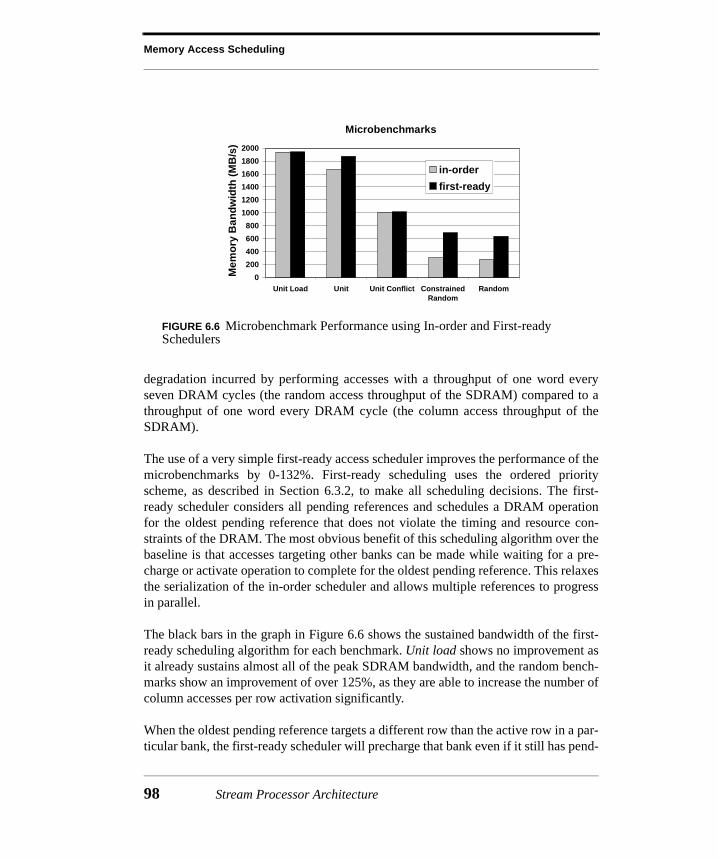
Memory Access Scheduling
degradation incurred by performing accesses with a throughput of one word everyseven DRAM cycles (the random access throughput of the SDRAM) compared to athroughput of one word every DRAM cycle (the column access throughput of theSDRAM).
The use of a very simple first-ready access scheduler improves the performance of themicrobenchmarks by 0-132%. First-ready scheduling uses the ordered priorityscheme, as described in Section 6.3.2, to make all scheduling decisions. The first-ready scheduler considers all pending references and schedules a DRAM operationfor the oldest pending reference that does not violate the timing and resource con-straints of the DRAM. The most obvious benefit of this scheduling algorithm over thebaseline is that accesses targeting other banks can be made while waiting for a pre-charge or activate operation to complete for the oldest pending reference. This relaxesthe serialization of the in-order scheduler and allows multiple references to progressin parallel.
The black bars in the graph in Figure 6.6 shows the sustained bandwidth of the first-ready scheduling algorithm for each benchmark. Unit load shows no improvement asit already sustains almost all of the peak SDRAM bandwidth, and the random bench-marks show an improvement of over 125%, as they are able to increase the number ofcolumn accesses per row activation significantly.
When the oldest pending reference targets a different row than the active row in a par-ticular bank, the first-ready scheduler will precharge that bank even if it still has pend-
FIGURE 6.6 Microbenchmark Performance using In-order and First-ready Schedulers
0
200
400
600
800
1000
1200
1400
1600
1800
2000
Unit Load Unit Unit Conflict ConstrainedRandom
Random
Mem
ory
Ban
dw
idth
(M
B/s
)
in-order
first-ready
Microbenchmarks
98 Stream Processor Architecture

Evaluation
ing references to its active row. More aggressive scheduling algorithms are requiredto further improve performance. Table 6.2 presents four aggressive scheduling algo-rithms that will further increase sustained memory bandwidth. The policies for eachof the schedulers in Table 6.2 are described in Section 6.3.2. The range of possiblememory access schedulers is quite large, and covering all of the schedulers examinedin Section 6.3 would be prohibitive. These four schedulers, however, are representa-tive of many of the important characteristics of an aggressive memory access sched-uler.
Figure 6.7 presents the microbenchmarks’ sustained memory bandwidth for eachmemory access scheduling algorithm. The aggressive scheduling algorithms signifi-cantly improve the memory bandwidth of the microbenchmarks over in-order sched-uling. Again the unit load benchmark shows no improvement. The unit conflictbenchmark, however, improves by 115% with more aggressive scheduling. All of thememory access scheduling algorithms considered are able to reorder accesses to theDRAM, so that references to conflicting banks to not interfere with each other in theDRAM. The random benchmarks improve by 125-250% with the more aggressivescheduling algorithms. They favor a closed precharge policy, in which banks are pre-charged as soon as no more pending references target their active row, because it isunlikely that there will be any reference locality that would make it beneficial to keepthe row open. By precharging as soon as possible, the access latency of future refer-ences is minimized. For most of the other benchmarks, the difference between anopen and a closed precharge policy is slight. Unit load is a notable exception, as itperforms worse with the col/closed algorithm. In this case, column accesses are satis-
AlgorithmColumn Access Precharging
Row Activation
Access Selection
col/openpriority
(ordered)open
priority (ordered)
column first
col/closedpriority
(ordered)closed
priority (ordered)
column first
row/openpriority
(ordered)open
priority (ordered)
row first
row/closedpriority
(ordered)closed
priority (ordered)
row first
TABLE 6.2 Memory Access Scheduling Algorithms
Memory Access Scheduling 99

Memory Access Scheduling
fied rapidly, emptying the bank buffer of references to a stream, allowing the banks tobe precharged prematurely in some instances.
6.4.2 Memory Demands
The memory performance of the microbenchmarks gives an indication of how muchbandwidth an application will be able to sustain, given that application’s memorybehavior. Table 6.3 shows the number and length of stream memory transfers in thefive applications presented in Chapter 3. The table shows that the applications makefrom 114 thousand to 2.3 million memory references over the course of their execu-tion. These references are part of over 25 thousand total stream transfers. The band-width demands on the memory system, presented previously in Section 5.4.3, are alsoshown in the table. These applications demand from 0.4 to 1.0GB/s of memory band-width to achieve their peak performance on Imagine.
The table shows that the vast majority of stream transfers use constant strides. Whilemany of these strided transfers use a unit stride, especially in DEPTH and MPEG, manydo not. For example, QRD and STAP frequently access the columns of matrices, usingvery large constant strides. The only applications that perform indirect stream trans-fers are MPEG and RENDER. In both of these applications, those accesses roughly cor-respond to the constrained random microbenchmark presented in the previoussection. MPEG performs indexed loads into the reference images during the motionestimation phase of P-frame encoding. As the motion in images is somewhat random,these references will also be somewhat random, but they will be constrained to liewithin the region of the reference image that was searched. RENDER performs indexed
FIGURE 6.7 Microbenchmark Performance Using Aggressive Schedulers
0
200
400
600
800
1000
1200
1400
1600
1800
2000
Unit Load Unit Unit Conflict ConstrainedRandom
Random
Mem
ory
Ban
dw
idth
(M
B/s
) in-orderfirst-readycol/opencol/closedrow/openrow/closed
Microbenchmarks
100 Stream Processor Architecture

Evaluation
loads and stores into the frame buffer and texture map. As pixels are rendered intoarbitrary locations, these references will also be somewhat random but constrained tothe frame buffer and texture map. There is some locality, in that adjacent pixels arelikely to lie close to each other in the frame buffer and access texels that are close toeach other as well. However, they may not necessarily reference pixels or texels thatare in consecutive locations in memory, as the frame buffer and texture map are storedin row major order and the renderer may traverse those structures in arbitrary direc-tions.
6.4.3 Application Performance
Application level experiments were performed both with and without the applica-tions’ computation. When running just the memory traces, dependencies from theapplication were maintained by assuming that the computation occurred at the appro-priate times but was instantaneous. The applications show the performance improve-ments that can be gained by using memory access scheduling on the Imagine streamprocessor. The applications’ memory traces, with instantaneous computation, showthe potential of the scheduling techniques as processing power increases and theapplications become entirely limited by memory bandwidth.
DEPTH MPEG QRD STAP RENDER Total
References (Thousands) 907.0 934.6 114.4 1900.6 2278.2 6134.7
Bandwidth Demand (GB/s)
0.99 0.45 0.42 0.65 0.76 0.64
Stride
Stream
Transfers
Loads 3131 83 19 3413 2630 9276
Avg. Length 185.4 842.0 3984.8 452.4 150.8 287.5
Stores 1440 324 78 2112 4050 8004
Avg. Length 226.7 1360.3 495.6 168.7 256.0 274.7
Indirect
Stream
Transfers
Loads 0 252 0 0 4074 4326
Avg. Length --- 1682.3 --- --- 172.8 260.7
Stores 0 0 0 0 3768 3768
Avg. Length --- --- --- --- 37.4 37.4
TABLE 6.3 Number and Length (in Words) of Stream Memory Transfers by Type
Memory Access Scheduling 101
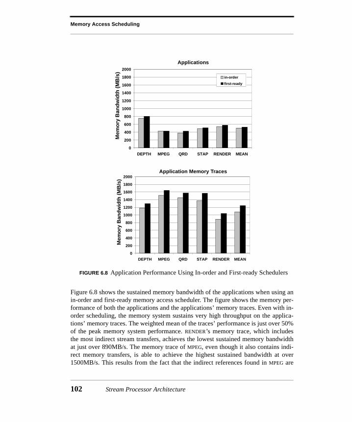
Memory Access Scheduling
Figure 6.8 shows the sustained memory bandwidth of the applications when using anin-order and first-ready memory access scheduler. The figure shows the memory per-formance of both the applications and the applications’ memory traces. Even with in-order scheduling, the memory system sustains very high throughput on the applica-tions’ memory traces. The weighted mean of the traces’ performance is just over 50%of the peak memory system performance. RENDER’s memory trace, which includesthe most indirect stream transfers, achieves the lowest sustained memory bandwidthat just over 890MB/s. The memory trace of MPEG, even though it also contains indi-rect memory transfers, is able to achieve the highest sustained bandwidth at over1500MB/s. This results from the fact that the indirect references found in MPEG are
FIGURE 6.8 Application Performance Using In-order and First-ready Schedulers
0
200
400
600
800
1000
1200
1400
1600
1800
2000
DEPTH MPEG QRD STAP RENDER MEAN
Mem
ory
Ban
dw
idth
(M
B/s
)
0
200
400
600
800
1000
1200
1400
1600
1800
2000
DEPTH MPEG QRD STAP RENDER MEAN
Mem
ory
Ban
dw
idth
(M
B/s
)
in-order
first-ready
Applications
Application Memory Traces
102 Stream Processor Architecture
Evaluation
far more constrained than those found in RENDER, so they exhibit much more rowlocality within the DRAMs.
When using an in-order scheduler, the applications are not always able to overlapmemory and computation successfully. The processor is stalled waiting for memoryan average of 21% of the time on these applications. However, these applications arecompute-bound for large portions of their execution. During those times, there are nooutstanding memory transfers, so the sustained memory bandwidth of the applica-tions is far lower than the sustained bandwidth of the memory traces. Across theapplications, the weighted mean of the sustained bandwidth for in-order scheduling isjust above 500MB/s, which is 25% of the peak memory bandwidth. The in-orderscheduler therefore provides 79% of the bandwidth demanded by the applications.
The improvements of first-ready scheduling are modest, both on the applications andthe memory traces. First-ready scheduling increases the memory bandwidth of theapplications by 4.5% and the memory traces by 14.8%. With a first-ready scheduler,the memory system supplies 82% of the bandwidth demanded by the applications.
Figure 6.9 shows the sustained memory bandwidth of the applications when using theaggressive memory access scheduling algorithms presented earlier in Table 6.2.Again, the figure shows the memory performance of both the applications and theapplications’ memory traces. The row/open scheduling algorithm performs best,improving the memory bandwidth of the applications by 8%, and the applications’memory traces by 51%. Some applications, such as MPEG, show very little improve-ment in performance with aggressive memory access scheduling. On the Imaginestream architecture, MPEG efficiently utilizes the SRF to capture locality. This makesMPEG compute-bound, so increasing the memory system bandwidth cannot improveperformance. However, the performance of the memory trace of MPEG achieves 94%of the peak bandwidth of the memory system when memory access scheduling isemployed.
All of the applications and traces slightly favor an address arbiter policy which selectsrow accesses first, rather than one that selects column accesses first. Also, algorithmsthat include an open page precharging policy outperform those with a closed pagepolicy, suggesting that these applications exhibit significant row locality in their refer-ence streams. The col/closed policy performs poorly across all of the applications andtraces in comparison with the other scheduling algorithms. As mentioned previously,this algorithm satisfies column accesses rapidly, emptying the bank buffer of refer-ences to a stream, allowing the banks to be precharged prematurely in some instances.The row/open scheduler delivers an average of 547MB/s to the applications and
Memory Access Scheduling 103

Memory Access Scheduling
1641MB/s to the application traces. With this algorithm, DEPTH, MPEG, and QRD arecompute-bound, and would require additional computation resources to improve per-formance. The memory system is able to deliver 79.5% and 87% of the memorybandwidth demanded by STAP and RENDER, respectively. Data dependencies constrainthese applications from further overlapping memory and computation, limiting theirpeak performance.
FIGURE 6.9 Application Performance Using Aggressive Schedulers
0
200
400
600
800
1000
1200
1400
1600
1800
2000
DEPTH MPEG QRD STAP RENDER MEAN
Mem
ory
Ban
dw
idth
(M
B/s
)
0
200
400
600
800
1000
1200
1400
1600
1800
2000
DEPTH MPEG QRD STAP RENDER MEAN
Mem
ory
Ban
dw
idth
(M
B/s
)
in-orderfirst-readycol/opencol/closedrow/openrow/closed
Applications
Application Memory Traces
104 Stream Processor Architecture
Summary
6.5 Summary
An effective bandwidth hierarchy can bridge the gap of over two orders of magnitudebetween modern DRAM bandwidth and the bandwidth required by the arithmeticunits. However, for such a hierarchy to be successful, the memory system must beable to sustain a significant fraction of the peak DRAM bandwidth. Five representa-tive media processing applications demand from 0.4 to 1.0GB/s of memory band-width to achieve their peak computation rates. On the Imagine stream processor, thiscorresponds to 20-50% of the peak DRAM bandwidth. A streaming memory systemwhich employs memory access scheduling to take advantage of the structure of mod-ern DRAM can make many of these applications compute-bound, even on a processorwith 48 arithmetic units.
Simple unit stride accesses can easily achieve 97% of the bandwidth of modernDRAM. However, random accesses are only able to sustain 14% of the DRAM band-width. The difference in performance corresponds to the degradation incurred by per-forming an access once every seven DRAM cycles, which is the random accessthroughput of the DRAM, compared to a throughput of one word every DRAM cycle,which is the column access throughput of the DRAM. Memory access schedulingcloses this gap, and improves the performance across several microbenchmarks by anaverage of 144%. In practice, media processing applications make many stream refer-ences with constant strides, but they also access large two-dimensional buffers witharbitrary reference patterns. By scheduling these stream references to take advantageof the locality and concurrency of modern DRAM, the sustained memory bandwidthfor media processing applications can make many media applications compute-boundand can increase the sustained bandwidth for the applications’ memory traces by anaverage of 51%.
Memory access scheduling improves the sustainable throughput of modern DRAMby reordering memory references to exploit the available bank parallelism and rowlocality. As DRAM evolves, techniques such as memory access scheduling will con-tinue to be necessary to overcome the non-uniform access times of the memoryarrays. However, the techniques and algorithms described here could be integratedinto the DRAM itself, with some modifications to enable the memory controller tointeract with the scheduler.
Memory Access Scheduling 105
Memory Access Scheduling
106 Stream Processor Architecture
CHAPTER 7 Conclusions
The major contribution of this work is a bandwidth-efficient stream architecture formedia processing. VLSI constraints motivate a data bandwidth hierarchy to provideenough data bandwidth to support the demands of media processing. In modernVLSI, hundreds of arithmetic units can fit on an inexpensive chip, but communicationamong those arithmetic units is expensive in terms of area, power, and delay. Conven-tional storage hierarchies do not provide enough data bandwidth to support largenumbers of arithmetic units. In contrast, a bandwidth hierarchy effectively feedsnumerous arithmetic units by scaling data bandwidth across multiple levels. Thisbridges the gap between the bandwidth available from modern DRAM and the band-width demanded by tens to hundreds of arithmetic units.
This work also contributes the design and evaluation of the Imagine stream processorarchitecture to take advantage of the characteristics of media processing applicationssubject to the constraints of modern VLSI. The Imagine stream processor implementsa data bandwidth hierarchy and memory access scheduling to efficiently provide databandwidth to 48 arithmetic units. When expressed in the stream programming model,media processing applications map naturally to the data bandwidth hierarchy and areable to efficiently utilize data bandwidth that is scaled across the levels of the hierar-chy. Imagine is, therefore, able to execute media processing applications at high sus-tained computation rates.
The stream programming model exposes the locality and concurrency of media pro-cessing applications so these characteristics can effectively be exploited by a stream
Conclusions 107

Conclusions
processor. In this model, applications are expressed as a sequence of computation ker-nels that operate on streams of data. This exposes the locality and concurrency bothwithin and among kernels, and enables the applications to effectively utilize a three-tiered data bandwidth hierarchy. At the base of the bandwidth hierarchy, memoryaccess scheduling maximizes the throughput of modern DRAM enabling applicationsto sustain 79-96% of the memory bandwidth they demand. At the center of the hierar-chy, the global stream register file provides a factor of 16 times more bandwidth thanthe memory system and enables data streams to be recirculated from kernel to kernelwithout consuming costly memory bandwidth. At the top of the bandwidth hierarchy,numerous local distributed register files feed 48 arithmetic units efficiently with a fac-tor of 17 times more bandwidth than the stream register file. These local register filesenable temporary storage of local kernel data so that more expensive global registerbandwidth is only consumed to recirculate data streams. Imagine achieves 4 to18GOPS of sustained computation on representative media processing applicationsusing both the bandwidth hierarchy and memory access scheduling.
7.1 Imagine Summary
Imagine is a programmable media processor that matches the demands of media pro-cessing applications to the capabilities of modern VLSI technology. Imagine imple-ments a stream architecture, which includes an efficient data bandwidth hierarchy anda streaming memory system. The bandwidth hierarchy bridges the gap between the2GB/s memory system and the arithmetic units that require 544GB/s to achieve theirfull utilization. At the base of the bandwidth hierarchy, the streaming memory systemsustains a significant fraction of the available DRAM bandwidth, enabling media pro-cessing applications to take full advantage of the bandwidth hierarchy.
The bandwidth hierarchy enables Imagine to achieve 77-96% of the performance of astream processor with infinite memory and global data bandwidth. Kernels make effi-cient use of local register files for temporary storage to supply the arithmetic unitswith data and of the stream register file to supply input streams to the arithmetic unitsand store output streams from the arithmetic units. The stream register file efficientlycaptures the locality of stream recirculation within media processing applications,thereby limiting the bandwidth demands on off-chip memory. When mapped to thethree-tiered storage hierarchy, the bandwidth demands of media processing applica-tions are well-matched to the provided bandwidth which is scaled by a ratio of1:16:276 across the levels of the hierarchy.
108 Stream Processor Architecture

Future Architectures
Memory access scheduling improves the performance of media processing applica-tions on Imagine by an average of 8%, making many applications compute-bound,even with 48 arithmetic units. Simple unit stride accesses can easily achieve 97% ofthe bandwidth of modern DRAM. However, random accesses are only able to sustain14% of the DRAM bandwidth without memory access scheduling. The difference inperformance corresponds to the degradation incurred by performing an access onceevery seven DRAM cycles (the random access throughput of the DRAM), comparedto a throughput of one word every DRAM cycle (the column access throughput of theDRAM). Memory access scheduling closes this gap and improves the performanceacross several representative microbenchmarks by an average of 144%. Using anaggressive scheduler that exploits the row locality and bank parallelism of the refer-ence stream, Imagine is able to improve the bandwidth of application memory tracesby an average of 51% and to provide 79-96% of the memory bandwidth demanded bymedia processing applications.
Imagine is designed to fit on a 2.5cm2 chip and operate at 500MHz in a 0.15µmCMOS standard-cell implementation. The peak computation rate of the 48 arithmeticunits is 20GOPS for both 32-bit integer and floating-point operations. For 16-bit and8-bit parallel-subword operations, the peak performance increases to 40 and 80GOPS,respectively. Applications achieve a significant fraction of this peak rate. For exam-ple, an MPEG encoder can sustain 18GOPS on 16-bit data.
7.2 Future Architectures
Microprocessors have traditionally included a storage hierarchy consisting of DRAM,caches, and a global register file. This organization is optimized to minimize the arith-metic units’ latency to access data. The register file is typically small enough that itcan be accessed in a single cycle. The cache hierarchy keeps data that is likely to beaccessed soon close to the arithmetic units to minimize the latency of memory opera-tions. The slow DRAM is used as a large storage area that is only accessed when thecache hierarchy does not hold the referenced data.
The effectiveness of the cache hierarchy is deceptive, as many of the advantages of acache arise from the fact that register files are too small. A cache relies on data reuseto reduce latency. An inadequately sized register file artificially inflates the amount ofdata reuse within an application. For example, the FIR filter example of Chapter 5showed that the coefficients of the filter needed to be reloaded from memory for thecomputation of every set of outputs. If the register file were larger, then these coeffi-
Conclusions 109
Conclusions
cients could be kept in registers, rather than the cache, and would then only beaccessed outside the register file once, at the start of execution. Similarly, temporarydata produced during the course of a computation is frequently spilled to memorybecause the register file is not large enough. Again, the cache captures this artificialdata reuse by holding that data until it is reloaded into the register file.
For applications with latency tolerance, as found in media processing, data can beprefetched far in advance of its use. Ideally, that data would be loaded into registers,but small register files do not have space for both the current data and the prefetcheddata. A cache can hold this prefetched data, again making the cache appear beneficial.Therefore, a cache’s effectiveness is largely due to the fact that modern VLSI con-strains global register files that directly feed arithmetic units to be small.
A cache can also limit the available bandwidth for the arithmetic units and wasteexternal DRAM bandwidth, making it difficult to bridge the data bandwidth gap. Acache is an inefficient way to stage data from memory because address translation isrequired on every reference, accesses are made with long memory addresses, somestorage within the cache must be allocated to address tags, and conflicts may evictpreviously fetched data that will be referenced in the future. These inefficienciesmake it difficult to scale the bandwidth of a cache without dramatically increasing itscost. Furthermore, an ineffective cache actually wastes external DRAM bandwidth.Cache line fetches retrieve more than one word from the DRAM on every cache miss.If these words are not all accessed, then DRAM bandwidth was wasted transferringthe entire line. Similarly, writing back data can waste bandwidth. A write-throughpolicy will always write stored data back to the DRAM. This is particularly wastefulif the data is actually temporary data that was spilled to memory due to limited regis-ter space. That temporary data will never be referenced again after it is reloaded intothe register file, so it did not need to return to DRAM. A write-back policy will usu-ally write the entire cache line back to DRAM, again wasting bandwidth if not all ofthe words in the line are dirty.
As the number of arithmetic units in a processor rises, data bandwidth becomesincreasingly important. Since a cache is optimized to minimize latency rather thanmaximize bandwidth, the traditional storage hierarchy needs to be reconsidered forprocessors that contain tens to hundreds of arithmetic units. For example, an explic-itly managed bandwidth hierarchy is a far more efficient use of resources for mediaprocessing applications. A global stream register file does not incur the overhead of acache and is able to provide far more data bandwidth through a single, wide port.Similarly, local distributed register files do not suffer from the bandwidth bottlenecks
110 Stream Processor Architecture
Future Architectures
of a global register file, so they can effectively support larger numbers of arithmeticunits.
A programming model that exposes the locality and concurrency of applications isrequired to utilize an explicitly managed storage hierarchy effectively. The traditionalsequential programming model hides parallelism and locality, making it difficult toextract parallel computations and manage data movement. The stream programmingmodel, however, enables parallelism to be readily exploited and makes most datamovement explicit. This enables a media processor to store data and perform compu-tations more efficiently.
This work demonstrates the need for future media processors to be designed to maxi-mize the data bandwidth delivered to the arithmetic units. Without sufficient databandwidth, media processors will not be able to support enough arithmetic units tomeet the demands of compelling media applications. The traditional storage hierarchyfound in most programmable processors is unable to provide enough data bandwidthto support tens to hundreds of arithmetic units, both because the hardware structuresare inefficient and because the supported programming model hides the locality andconcurrency of the applications. Communication-limited VLSI technology makes itdifficult to extract locality and concurrency dynamically.
Therefore, future media processors must provide an explicitly managed storage hier-archy, scale data bandwidth between external DRAM and the arithmetic units, andprovide local communication and storage resources. An explicitly managed storagehierarchy can minimize global communication by allowing the compiler to be awareof expensive communication and storage. This motivates the compiler to utilize inex-pensive bandwidth when possible and resort to more expensive bandwidth only whennecessary. The bandwidth between external DRAM and the arithmetic units must bescaled in order to support large numbers of arithmetic units. Without this scaling, uti-lization will ultimately be limited by memory bandwidth. Finally, local communica-tion and storage resources are required to enable temporary data to be efficientlystored and communicated among arithmetic units. The traditional global register fileorganization severely limits the sustainable computation rate by requiring global databandwidth to be used for local data transfers and memory bandwidth to be used forintermediate data storage. Local register files can be utilized to store local data andprovide efficient bandwidth to the arithmetic units, which frees up the global registerfile to hold intermediate values and prevent them from accessing external DRAMunless absolutely necessary. Bandwidth-efficient architectures are therefore requiredto overcome the communication-limited nature of modern VLSI.
Conclusions 111
Conclusions
112 Stream Processor Architecture

References
[BW95] V. Michael Bove, Jr. and John A. Watlington. Cheops: A ReconfigurableData-Flow System for Video Processing. IEEE Transactions on Circuitsand Systems for Video Technology (April 5, 1995), pp. 140-149.
[BGK97] Doug Burger, James R. Goodman, and Alain Kägi. Limited Bandwidthto Affect Processor Design. IEEE Micro (November/December 1997),pp. 55-62.
[CTW97] Kenneth C. Cain, Jose A. Torres, and Ronald T. Williams. RT_STAP:Real-Time Space-Time Adaptive Processing Benchmark. TechnicalReport MTR 96B0000021, The MITRE Corporation, Bedford MA,February 1997.
[CHS+99] John Carter, Wilson Hsieh, Leigh Stoller, Mark Swanson, Lixin Zhang,Erik Brunvand, Al Davis, Chen-Chi Kuo, Ravindra Kuramkote, MichaelParker, Lambert Schaelicke, and Terry Tateyama. Impulse: Building aSmarter Memory Controller. Proceedings of the Fifth InternationalSymposium on High Performance Computer Architecture (January1999), pp. 70-79.
[CEV98] Jesus Corbal, Roger Espasa, and Mateo Valero. Command VectorMemory Systems: High Performance at Low Cost. Proceedings of the1998 International Conference on Parallel Architectures andCompilation Techniques (October 1998), pp. 68-77.
References 113
References
[Cri97] Richard Crisp. Direct Rambus Technology: The New Main MemoryStandard. IEEE Micro (November/December 1997), pp. 18-28.
[CJDM99] Vinodh Cuppu, Bruce Jacob, Brian Davis, and Trevor Mudge. APerformance Comparison of Contemporary DRAM Architectures.Proceedings of the International Symposium on Computer Architecture(May 1999), pp. 222-233.
[Die99] Keith Diefendorff. Pentium III = Pentium II + SSE. MicroprocessorReport (March 1999), pp. 1-7.
[FvFH96] James D. Foley, Andries van Dam, Steven K. Feiner, and John F.Hughes. Computer Graphics: Principles and Practice, Addison-WesleyPublishing Company: Menlo Park, California, 1996.
[Fol96] Pete Foley. The Mpact Media Processor Redefines the Multimedia PC.Proceedings of COMPCON (February 1996), pp. 311-318.
[Gla99] Peter N. Glaskowsky. Most Significant Bits: NVIDIA GeForce offersacceleration. Microprocessor Report 13(12), 1999.
[GV96] Gene H. Golub and Charles F. Van Loan. Matrix Computations, ThirdEdition, The John Hopkins University Press: Baltimore, Maryland, 1996.
[GMG89] A. Gunzinger, S. Mathis, and W. Guggenbühl. The SYnchronousDAtaflow MAchine: Architecture and Performance. Proceedings ofParallel Architectures and Languages Europe (June 1989), pp. 85-99.
[HG97] Ziyad S. Hakura and Anoop Gupta. The Design and Analysis of a CacheArchitecture for Texture Mapping. Proceedings of the InternationalSymposium on Computer Architecture (June 1997),pp. 108-120.
[HMS+99] Sung I. Hong, Sally A. McKee, Maximo H. Salinas, Robert H. Klenke,James H. Aylor, and William A. Wulf. Access Order and EffectiveBandwidth for Streams on a Direct Rambus Memory. Proceedings of theFifth International Symposium on High Performance ComputerArchitecture (January 1999), pp. 80-89.
[HL99] Tim Horel and Gary Lauterbach. UltraSPARC-III: Designing Third-Generation 64-Bit Performance. IEEE Micro (May/June 1999), pp. 73-85.
[Jac96] Keith Jack. Video Demystified: A Handbook for the Digital Engineer,LLH Technology Publishing: Eagle Rock, Virginia, 1996.
114 Stream Processor Architecture
[Jou90] Norman P. Jouppi. Improving Direct-Mapped Cache Performance by theAddition of a Small Fully-Associative Cache and Prefetch Buffers.Proceedings of the International Symposium on Computer Architecture(May 1990),pp. 364-373.
[KDR+00] Ujval Kapasi, William J. Dally, Scott Rixner, Peter Mattson, and John D.Owens. Efficient Conditional Operations for Data-ParallelArchitectures. Proceedings of the International Symposium onMicroarchitecture (December 2000).
[Kes99] R. E. Kessler. The Alpha 21264 Microprocessor. IEEE Micro (March/April 1999), pp. 24-36.
[KKK95] Takeo Kanade, Hiroshi Kano, and Shigeru Kimura. Development of aVideo-Rate Stereo Machine. Proceedings of the International Roboticsand Systems Conference (August 1995), pp. 95-100.
[Koz99] Christoforos Kozyrakis. A Media-Enhanced Vector Architecture forEmbedded Memory Systems. Technical Report UCB/CSD-99-1059,University of California Computer Science Division, Berkeley, CA, July1999.
[Kro81] David Kroft. Lockup-Free Instruction Fetch/Prefetch CacheOrganization. Proceedings of the International Symposium on ComputerArchitecture (May 1981), pp. 81-87.
[LS98] Corinna G. Lee and Mark G. Stoodley. Simple Vector Microprocessorsfor Multimedia Applications. Proceedings of the InternationalSymposium on Microarchitecture (December 1998), pp. 25-36.
[Lee96] Ruby B. Lee. Subword Parallelism with MAX-2. IEEE Micro (August,1996), pp. 51-59.
[Lin82] N. R. Lincoln. Technology and Design Tradeoffs in the Creation of aModern Supercomputer. IEEE Transactions on Computers (May 1982),pp. 363-376.
[Lip68] J. S. Liptay. Structural Aspects of the System/360 Model 85, Part II: TheCache. IBM Systems Journal 7:1 (1968), pp. 15-21.
[MMCD00] Binu K. Matthew, Sally A. McKee, John B. Carter, and Al Davis. Designof a Parallel Vector Access Unit for SDRAM Memory Systems.Proceedings of the Sixth International Symposium on High-PerformanceComputer Architecture (January 2000), pp. 39-48.
References 115

References
[MDR+00] Peter Mattson, William J. Dally, Scott Rixner, Ujval J. Kapasi, and JohnD. Owens. Communication Scheduling. Proceedings of the InternationalConference on Architectural Support for Programming Languages andOperating Systems (November 2000).
[MW95] Sally A. McKee and William A. Wulf. Access Ordering and Memory-Conscious Cache Utilization. Proceedings of the First Symposium onHigh Performance Computer Architecture (January 1995), pp. 253-262.
[MBDM97] John S. Montrym, Daniel R. Baum, David L. Dignam, and ChristopherJ. Migdal. InfiniteReality: A Real-Time Graphics System. Proceedingsof SIGGRAPH (August 1997), pp. 293-302.
[NEC98] NEC Corporation. 128M-bit Synchronous DRAM 4-bank, LVTTL DataSheet. Document No. M12650EJ5V0DS00, 5th Edition, Revision K(July 1998).
[Nit99] Ramon Nitzberg. Radar Signal Processing and Adaptive Systems,Artech House: Boston, MA, 1999.
[Oed92] Wilfried Oed. Cray Y-MP C90: System features and early benchmarkresults. Parallel Computing (August 1992), pp. 947-954.
[OSB99] Alan V. Oppenheim and Ronald W. Shafer with John R. Buck. Discrete-Time Signal Processing, Second Edition, Prentice Hall: Upper SaddleRiver, NJ, 1999.
[ODK+00] John Owens, William J. Dally, Ujval J. Kapasi, Scott Rixner, PeterMattson, and Ben Mowery. Polygon Rendering on a StreamArchitecture. Proceedings of the Eurographics/SIGGRAPH Workshopon Graphics Hardware (August 2000).
[PW96] Alex Peleg and Uri Weiser. MMX Technology Extension to the IntelArchitecture. IEEE Micro (August, 1996), pp. 42-50.
[RS96] Selliah Rathnam and Gerrit A. Slavenburg. An Architectural Overviewof the Programmable Multimedia Processor, TM-1. Proceedings ofCOMPCON (February 1996), pp. 319-326.
[RDK+98] Scott Rixner, William J. Dally, Ujval J. Kapasi, Brucek Khailany,Abelardo López-Lagunas, Peter R. Mattson, and John D. Owens. ABandwidth-Efficient Architecture for Media Processing. Proceedings ofthe International Symposium on Microarchitecture (December 1998),pp. 3-13.
116 Stream Processor Architecture
[RDK+00a] Scott Rixner, William J. Dally, Ujval J. Kapasi, Peter Mattson, and JohnD. Owens. Memory Access Scheduling. Proceedings of the InternationalSymposium on Computer Architecture (June 2000), pp. 128-138.
[RDK+00b] Scott Rixner, William J. Dally, Brucek Khailany, Peter Mattson, Ujval J.Kapasi, and John D. Owens. Register Organization for MediaProcessing. Proceedings of the Sixth Symposium on High PerformanceComputer Architecture (January 2000), pp. 375-386.
[Rus78] Richard M. Russell. The Cray-1 Computer System. Communications ofthe ACM (January 1978), pp. 63-72.
[SV89] R. Schreiber and C. Van Loan. A storage-efficient WY representation forproducts of Householder transformations. SIAM J. Scientific andStatistical Computing, 10(1):53--57, 1989.
[Sed90] Robert Sedgewick. Algorithms in C, Addison-Wesley PublishingCompany, 1990.
[TH99] Shreekant Thakkar and Tom Huff. Internet Streaming SIMD Extensions.Computer (December 1999), pp. 26-34.
[TONH96] Marc Tremblay, J. Michael O’Connor, Venkatesh Narayanan, and LiangHe. VIS Speeds New Media Processing. IEEE Micro (August, 1996), pp.10-20.
[TH97] Jim Turley and Harri Hakkarainen. TI’s New 'C6x DSP Screams at 1,600MIPS. Microprocessor Report (February 17, 1997), pp. 14-17.
[VPPL94] H. Veendrick, O. Popp, G. Postuma, and M. Lecoutere. A 1.5 GIPS videosignal processor (VSP). Proceedings of the IEEE Custom IntegratedCircuits Conference (May 1994), pp. 95-98.
[WAM+99] Takeo Watanabe, Kazushige Ayukawa, Seiji Miura, Makoto Toda,Tetsuya Iwamura, Kouichi Hoshi, Jun Sato, and KazumasaYanagisawa.Access Optimizer to Overcome the “Future Walls of EmbeddedDRAMs” in the Era of Systems on Silicon. IEEE International Solid-State Circuits Conference Digest of Technical Papers (February 1999),pp. 370-371.
[YHO97] Tadaaki Yamauchi, Lance Hammond, and Kunle Olukotun. TheHierarchical Multi-bank DRAM: A High-Performance Architecture forMemory Integrated with Processors. Proceedings of the Conference onAdvanced Research in VLSI (September 1997), pp. 303-319.
References 117

References
118 Stream Processor Architecture

Index
AAddress arbiter 93Address generators 40–41Arithmetic clusters 6, 8, 37–38
BBandwidth hierarchy
See Data bandwidth hierarchyBandwidth sensitivity 78–79
CCache hierarchy 55–59, 109Centralized register file 58Cheops 13Column arbiter 93–94Conditional streams 48Cray-1 14
DData bandwidth hierarchy 1, 4–6, 9, 27, 53–
82, 107–108Distributed register files 38, 61
See also Local register filesDRAM 59–60, 83, 86, 88–91, 107, 109–110
FFIR filter 65–72
Index
HHost processor 43
IImagine media processor 7–8, 27–52, 66–
82, 108–109InfiniteReality 11–12iscd 31
KKernel 2, 16, 29, 44, 108KernelC 31, 47
LLocal register files 4–5, 27, 49, 54, 67, 110
MMAX-2 12
119

Index
Memory access scheduling 9, 83–105, 109algorithms
col/closed 99, 103col/open 99first-ready 87, 98, 103in-order 87–88, 97, 103row/closed 99row/open 88, 99
architecture 92–94policies
closed 95column-first 95fewest-pending 95in-order 94most-pending 95open 94precharge-first 95priority 94row-first 95
Memory address register file 41Memory demands 100–101Microcontroller 8, 39MMX 12, 66–72Mpact 12MPEG2 encoder 2, 20, 30–34, 72–82, 84–
86, 101–104MSHR 42
NNetwork interface 8, 42–43Network route register file 42NVIDIA GeForce 12
PParallel Vector Access unit 15Parallel-subword instructions 37Polygon renderer 21, 76–82, 101–104Precharge manager 93–94
QQR decomposition 21, 76–82, 101–104
RRecord 29, 41Register file scaling 58, 61–63Reorder buffers 40Row arbiter 93–94
120 Stream Processor Architectu
SSIMD 6, 13, 27, 37, 47, 63Space-time adaptive processing 21, 76–82,
101–104SSE 12Stereo depth extraction 20, 76–82, 101–104Stream 3, 16, 29, 44, 108Stream architecture 2–7, 34–44Stream buffers
for the memory system 15for the SRF 35–36, 62
Stream controller 8, 43Stream instructions
barrier 46clustop 46load 46move 45read 45receive 46send 46store 46synch 46write_imm 45
Stream Memory Controller 15Stream programming model 2–3, 29–30,
44–48, 55, 68, 107, 111Stream recirculation 64, 72, 75, 82Stream register file (SRF) 4–5, 8, 27–28,
35–36, 49, 52, 54, 62, 67, 86, 110Stream scheduler 32StreamC 32–33, 44Streaming memory system 4, 6, 8, 17, 27,
40–42, 49, 54, 84SYDAMA 13
TTMS320C6000 4, 14, 58, 66–72TriMedia 12
VVector processors 13VIS 12VLIW 6, 31, 37, 39VRAM 14VSP 12
re