
BY ARTHUR DELAGRANGE WEAPONS … ARTHUR DELAGRANGE WEAPONS SYSTEMS DEPARTMENT-DTI C 13 JULY 1993...
16
NSWCDD/TR-93/332 AD--A267 568 / AN 8X-REAL-TIME DIFAR MULTIPLEXER- DEMULTIPLEXER SYSTEM BY ARTHUR DELAGRANGE WEAPONS SYSTEMS DEPARTMENT -DTI C 1AUG0 41993 13 JULY 1993 . •.i Approved for public release; distribution is unlimited. 93-17467 NAVAL SURFACE WARFARE CENTER DAHLGREN DIVISION .WHITE OAK DETACHMENT Silver Spring. Maryland 20903.5640 s ..a
Transcript of BY ARTHUR DELAGRANGE WEAPONS … ARTHUR DELAGRANGE WEAPONS SYSTEMS DEPARTMENT-DTI C 13 JULY 1993...

NSWCDD/TR-93/332 AD--A267 568 /
AN 8X-REAL-TIME DIFAR MULTIPLEXER-DEMULTIPLEXER SYSTEM
BY ARTHUR DELAGRANGE
WEAPONS SYSTEMS DEPARTMENT
-DTI C1AUG0 4199313 JULY 1993 . •.i
Approved for public release; distribution is unlimited.
93-17467
NAVAL SURFACE WARFARE CENTERDAHLGREN DIVISION .WHITE OAK DETACHMENT
Silver Spring. Maryland 20903.5640
s ..a

NSWCDD/TR-92/332
AN 8X-REAL-TIME DIFAR MULTIPLEXER-DEMULTIPLEXER SYSTEM
BY ARTHUR DELAGRANGE
WEAPONS SYSTEMS DEPARTMENT
13 JULY1993
Approved for public release; distribution is unlimited.
NAVAL SURFACE WARFARE CENTERDAHLGREN DIVISION *WHITE OAK DETACHMENT
Silver Spring, Maryland 20903-5640

NSWCDD/TR-92/332
FOREWORD
DIFAR multiplexers and demultiplexers designed by the Center's U20 Divisionwere described in detail in NAVSWC TR 91-334. This report describes the circuitryof an 8X-real-time version of the system developed for high-speed demultiplexing oftape-recorded data.
Approved by:
DAVID S. MALYEVAC, Deputy HeadWeapons Systems Department
DTIC QUALITY r1•rTGED 3
AcoesinnFor
P ', .. ... 7"p- ... . -
' "I II D 7 I I I
NSWCDD/TR-92/332
ABSTRACT
DIFAR multiplexers and demultiplexers designed by the Acoustic SignalProcessing Branch, Naval Surface Warfare Center Dahlgren Division, have beendescribed in a previous report. This report describes modifications to make thesystem work at 8X-real-time, primarily for high-speed demultiplexing of tape-recorded data.
NSWCDDITR-92/332
CONTEiNTS
Page
INTRODUCTION ...................................................... 1
CIRCU ITRY ........................................................... 1
CON CLU SION ........................................................ 2
APPENDIX A: MULTIPLEXER CHECKOUT AND ADJUSTMENT ....... A-1
APPENDIX B: DEMULTIPLEXER CHECKOUT AND ADJUSTMENT .... B-1
DISTRIBU TION ....................................................... (1)
Illoi
NSWCDD/TR-92/332
ILLUSTRATIONS
Figure Page
1 M ultiplexer Input Filters ..................................... 3
2 Multiplexer Summing Circuit ................................. 4
3 Demultiplexer Phase-Lock Loop Circuit ........................ 5
4 Demultiplexer Output Filter Circuits .......................... 6
iv
NSWCDD/TR-92/332
INTRODUCTION
DIFAR multiplexers and demultiplexers designed by the Acoustic Signal ProcessingBranch have been in use for a number of years. Recently a redesign was completedand a report publishedl. Concurrently a limited effort was made to make thecircuitry operate eight times faster. This would speed the job of reducing volumes oftaped multiplexed data to (taped) demultiplexed data.
The effort was partially successful. The system works, but dipole channel separationis only about 25 dB, vice 30 + dB for the normal system.
Theory and operation of the basic system is given in detail in Reference 1 and will notbe repeated here, as it all applies here if the numbers are simply changed by a factorof eight. The new circuit diagrams are given, and the changes are described in thetext.
CIRCUITRY
A ground rule was that the existing circuit boards had to be used with only slightmodification. Thus, primarily, only components were changed, although a fewtopography changes were "hacked in" on the boards. Considerable care wasnecessary to make even the original boards work properly, as maintaining a fractionof a degree of phase accuracy at 15 kHz implies logic rise and delay times of less than100 nsec, and maintaining gain accuracies better than 1% implies analog bandwidthsof several megahertz. Readily available integrated circuits were adequate for thestandard system, but not for the 8X faster system. In some cases high-speed versionsof deficient circuits were not available.
Although the multiplexer input filters (Figure 1) operate linearly and pass only 40kHz, they must reject higher frequencies properly without going nonlinear. Also, the"supercapacitor" circuits require considerable extra bandwidth as they areessentially part of tuned circuits. Substitution of newer, higher-speed quad op-ampsin these gave a reasonable filter response. However, an unanswered question is:How much variation is to be expected between channels, as mismatch directly affectsthe amplitude accuracy of the signals.
Otherwise, the changes are simply changes in the values of the passive components toreflect the effectively 8X higher frequencies. This could have been done simply byreducing all capacitors by a factor of eight, but doing that would have given a
1 Delagrange, A. D., DIFAR Multiplexer-demultiplexer System, Latest Improvements, NAVSWC TR91-344, 1 May 1992, Naval Surface Warfare Center, White Oak, Md.
1

NSWCDD/TR-92/332
nonstandard value not readily available; so instead the filter capacitors were reducedby a factor often and the resistors adjusted accordingly.
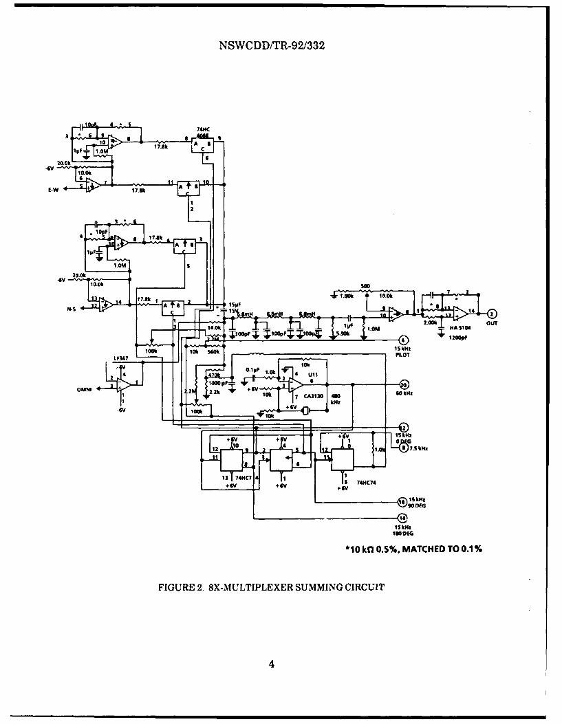
In the multiplexer output circuit (Figure 2), capacitors and inductors in the filtercircuit were reduced by a factor of 10, leaving the impedance unchanged. This gives acutoff frequency slightly higher than necessary, but this is not critical. The oscillatoris now 480 kHz.
In the demultiplexer phase-lock loop (Figure 3), values in the integrators have beenreduced to raise the loop speed by a factor of 10, reflecting the faster tape speed. Inthe 7.5-kHz (now 60-kHz) filter the capacitors have been reduced by a factor of 10 andthe resistors adjusted accordingly. New high-speed op-amps are used. These haverather high input current, and the resulting offset required that the comparatorfollowing be AC-coupled. Also, the more expensive grade of comparator is nowrequired to ensure adequate speed. The tuning inductor in the Voltage-Controlle'iOscillator (VCO) is reduced by a factor of 10; the Voltage-Variable Capacitor (VVC)already was the lowest value of the series. Fortunately, these need not be exact, asthe capacitor is automatically adjusted by the loop anyway.
The demultiplexer output filters (Figure 4) are the same as the multiplexer inputfilters already discussed, and the changes are identical.
CONCLUSION
Although theoretically all that is necessary to increase the speed (frequency) of thesystem is to reduce the values of the reactive components by a corresponding amount,in practice there is a number of problems as frequency is increased. The finite speedof the integrated circuits causes bigger relative errors. Stray capacitance becomesmore significant. It is desirable to keep the reactive components at common values,so juggling the resistor values is necessary.
Only prototypes were built, and limited testing was done. Some of the nicetieseventually added to the standard units are not included here, e.g., overload indicationfor the multiplexer. Substantial improvements to the circuitry are probably possibleonly through improved integrated circuits not yet on the market, or larger circuitboards to allow major changes in circuit design. However, the circuits are quiteusable in their present form, albeit at somewhat reduced accuracy.
2

NSWCDD/rTR-92/332
66
% IN
OMN j IO.
UNA1ERSITR +.f 1%ENA-ECPATR lOOpp 1%
UNARE INDUTOR 103 mHt
3.9
NSWCDD/TR-92/332
100L 4 574MC
3, 1 6 9 a 910
17.8kIIjF;; 1.0
20.Ok4V
10.0k6
E-W A 8
12
3
F I7..lk
+ A 8
I.om
20.Ok-6v 7 10. ;Gk
1.00k Soo 10.0k 7
A 8 1 SVFN-S c Is
14 2
2.00k OUT14.Ok IpF 1.0m HAS104
ý;IWF;J;;PO04 SANI"W
ISk100k 10k SW PILOTLF347
2 4 4 O.IpF i.Ok 2 4 ull
I pF ;-1 3 6
OMNI 2N 2.2 + GV 60 kHz10k CA3130 490kHz
+6V.6v 1410k
+fV ISkHz+ + I L"G
12 0 4 I.oh -- UN 7.S kHz
1 16
13 74HC7 1 3 74KC74+6V v
+ F6V + 6V'
A'-N IS kHzXZ/90 DEG
ia
ISkHzINDEG
*10 ka 0.5%, MATCHED TO 0.1%
FIGURE 2. 8X-MULTIPLEXER SUMMING CIRCUIT
4

NSWCDD/TR-92/332
*002
v 00
I-r
LLL
5

NSWCDD/TR-92/332
3.09k lpjf 100k I 10.0k 2k 21.51c
E-W~
1.13k 2 +1V280 624
139
T14 4- 8
12 4 10
NOTS: NMAKEDCAPCITRSLOpF1
AL 3NDUTOR 10 24
FIGUR 4.OUTULILXROUPTFLERCRUT
10k1

NSWCDD/TR-92/332
APPENDIX A
MULTIPLEXER CHECKOUT AND ADJUSTMENT
1. Insert card into rack or test fixture. Make sure supplies are adjusted to ± 6V ± 15mV. If supplies cannot be adjusted, recalibrate card with the same supply it isoperated with (step 3 primarily).
2. Check oscillator output (pin 20). It should be a square waveform, 0 to + 6V,480.000 kHz ± 300 Hz.
3. Set the three inputs pots haif way up. Observe the output (pin 2) with no signalsin. Ground pins 4 and 8. Adjust the two balance pots alternately for minimumoutput signal using a filter set at 120 kHz and a true-RMS AC voltmeter, or spectrumanalyzer obs.erving the 120-kHz line.
4. Ground pin 8 only. Output should be 120 kHz ±+ 120 Hz, fairly sinusoidal. Adjustoutput pot for 100 mVRMS (-20dBV).
5. Ground pin 4 only. Output should be 60 kHz ± 60 Hz, sinusoidal. Amplitudeshould be about 100 mVRMS. There is no adjustment.
6. Ground pins 4 and 8. Place a 10-kHz, 1-VRMS sine on OMNI in (pin 31). Adjustthe corresponding input pot for 0.707 VRMS (-3dBV) at output. Repeat for E-W in(pin 28). On a spectrum analyzer this will be -6dBV lines at 110 kttz and 130 kHz.Repeat for N-S in (pin 34). Place signal on all three inputs. Overload lamp shouldlight.
7. Check frequency response. For each of the three channels, increase inputfrequency until output level drops 3 dB from that at 10 kHz. Input frequency shouldbe 40 kHz ± 4 kHz.
8. As a double check, connect the multiplexer to a demultiplexer if available (thisstep is optional but it may show up problems the calibration procedure does notcatch). Place a 10-kHz 1-VRMS (0 dBV) sine wave on the N-S input. Lock lampshould be lit. Overload lamp should be dark. Check to see that the 10-kHz 1-VRMSinput signal appears at the N-S output. Move input signal to E-W input and check tosee that it appears at the E-W output. Move signal input to OMNI to see that itappears at OMNI output. Output level should be 0 dBV ± 0.3 dB for all three cases.Signal on the two unused channels should be below -25 dBV in all cases. Checkfrequency response for all three channels. It should be down 6 dB at 40 kHz ±4 kHz.On the low end it should drop less than 3 dB at 25 Hz. Check feedthrough and noiseat the outputs with no signals in. It should be below -50 dBV for each, true RMS.
A-1/A-2

NSWCDD/TR-92/332
APPENDIX B
DEMULTIPLEXER CHECKOUT AND ADJUSTMENT
1. Insert card into rack or test fixture. Make sure supplies are adjusted to ± 6V ± 15mV. If supplies cannot be adjusted, card should be readjusted with the same supply it isoperated with (step 3 primarily).
2. Place a 60-kHz, 100-mV RMS (-20dBV) sine wave on the input (pin 34). Adjust thepots for 180-degree phase shift through each section. Recheck filter to see that it peaksat 60 kHz ± 600 Hz.
3. Place a 200-kHz, 1-VRMS (OdBV) sine wave on the input (pin 34). Set the 120-kHzintegrator balance pot fully counterclockwise. The output (pin 27) should drift up toabout 4.5 V, reset to about + 3 V, drift up again, etc. Set the pot fully clockwise. Theoutput should drift dowii to about 1.5 V, reset to about +3 V, drift down again, etc.Adjust the pot for minimum drift of the 120-kHz integrator by observing the voltage atpin 27 with a voltmeter having at least 1-mV sensitivity.
4. Change input to 10 kHz. Adjust the OMNI pot for 1.4 VRMS ( + 3 dBV) at OMNIoutput (pin 24). Lock lamp should not light.
5. Place at the input a composite waveform consisting of a 130-kHz, 0.5-VRMS (-6 dBV)sine wave plus a 60-kHz, 0.5-VRMS (-6 dBV) rectangular wave of 75%, 25% duty cycle.Lock lamp should light. Overload lamp should not light. N-S (pin 26) and E-W (pin 22)outputs should be sine waves, 10 kHz. Adjust the dipole pots to give 0.5 VRMS (-6 dBV)at each. Increase the sine wave amplitude 10 dB. Overload lamp should come on.
6. Check the frequency response of the OMNI by inserting the signal of step 4 butincreasing the frequency until the OMNI output amplitude drops 3 dB. Frequencyshould be 40 kHz ± 4 kHz. Check the frequency response of each dipole by inserting thecomposite signal of step 5 but increasing the input sine wave frequency until the outputamplitude drops 3 dB. Output frequency should be 40 kHz7±4 kHz. Check feedthroughandnoise by observing the three outputs with no signal into the demultiplexer. Itshould be below -40 dBV for each, true RMS.
7. As a double check, connect a multiplexer to the demultiplexer if available (this stepis optional but it may show up problems the calibration procedure does not catch). Placea 10-kHz, 1-VRMS (0 dBV) sine wave on the N-S input. Lock lamp should light.Overload lamp should not light. Check to see that the 10-kHz, 1-VRMS input signalappears at the N-S output. Move the input signal to the E-W input and check to see thatit appears at the E-W output. Move the input signal to OMNI input and check to seethat it appears at the OMNI output. Ou Lput level should be 0 dBV ± 0.3 dB for all threecases. The signal on the two unused channels should be below -25 dBV in all cases.Check the frequency response for all three channels. It should be down 6 dB at 40 kHz± 4 kHz. Check feedthrough and noise at the outputs with no signals in. It should bebelow -50 dBV for each, true RMS.
B-1/B-2

NSWCDD/TR-92/332
DISTRIBUTION
Copies Covies
DOD ACTIVITIES (CONUS) NON-DOD ACTIVITIES
COMMANDING OFFICER 1 GREENERIDGE SCIENCES, INC I
NAVAL AIR DEVELOPMENT CENTER 4512 VIA HUERTO
WARMINSTER PA 18974 SANTA BARBARA CA 93110
ATTN OP-951 1 MAGNAVOXGOVERNMENT&OP-981 1 INDUSTRIAL ELECTRONICS CO I
OFFICE OF CHIEF OF NAVAL 1313 PRODUCTION RD
OPERATIONS FT WAYNE IN 46808
WASHINGTON DC 20350ATWN CARROLL BUSH
ATTN PMA-240 I SPARTON ELECTRONICS
PMA-244 1 2400 EAST GANSON STREET
PMA-264 I JACKSON MI 49202
370 1533042 1
COMMAN DER INTERNALNAVAL AIR SYSTEMS COMMANDWASHINGTON DC 20361 E231 2
E232 3
ATTN PMS-411 1 G94 A DELAGRANGE 10
COMMANDER G94 W BEATTY 1
NAVAL SEA SYSTEMS COMMAND G94 J FRENCH 1
NAVAL SEA SYSTEMS COMMAND N51 M WILLIAMS 1
HEADQUARTERS N501 T BALLARD I
WASHINGTON DC 20362
DEFENSE TECHNICALINFORMATION CENTER 12
CAMERON STATIONALEXANDRIA VA 23314
(1)/(2)
Form ApprovedREPORT DOCUMENTATION PAGE OMB No. 0704-0188
Pubhc reporting burden for this collection of information is estimated to average I hour petr response, including the time for reviewing instructions, searching existing datasources, gathering and maintaining the data needed, and completing and reviewing the collection of information. Send comments regarding this burden estimate or any otheraspect of this collection of information, including suggestions for reducing this burden, to Washington Headquarters Services. Directorate for Information Operations andReports, 12 15 Jefferson Davos Highway, Suite 1204. Arlington, VA 22202-4302, and to the Office of Management and Budget, Paperwork Reduction Project (0704 0188),Washington. DC 20503
1. AGENCY USE ONLY (Leave blank) 2. REPORT DATE 3. REPORT TYPE AND DATES COVERED
I Aug 1992 Final
4. TITLE AND SUBTITLE 5. FUNDING NUMBERS
An 8X-Iteal-Time D)I FAR Multiplexer-Deniultiplexer System 603708N W0490
6. AUTHOR(S) A5465461 009C
Arthur 1). D)elagrange
7. PERFORMING ORGANIZATION NAME(S) AND ADDRESS(ES) 8. PERFORMING ORGANIZATIONREPORT NUMBER
Naval Surface Warfare Center (U25)10901 New I lampshire Avenue NSWCI)!) fi'R-92/332
Silver Spring, Maryland 20903-5000
9. SPONSORINGIMONITORING AGENCY NAME(S) AND 10.SPONSORING/MONITORINGAGENCY REPORT NUMBER
11. SUPPLEMENTARY NOTES
12a. DISTRIBUTION/AVAILABILITY 12b. DISTRIBUTION CODE
13. ABSTRACT (Maximum 200 words)
I)NFA It multiplexers and demultiplexers designed by the Acoustic Signal Processing Branch, NavalSurface Warfare Center l)ahlgren Division, have been described in a previous report. This reportdescribes modifications to make the system work at 8X real time, primarily for high-speeddemultiplexing of tape-recorded data.
14. SUBJECT TERMS 15. NUMBER OF PAGES
l)IFAR _____________
MU LTI!L.EXI"R 16. PRICE CODEDI)1'MU U i,'i11. X !ER1
17. SECURITY CLASSIFICATION 18. SECURITY CLASSIFICATION 19. SECURITY CLASSIFICATION 20. UMITATION OFOF REPORT OF THIS PAGE OF ABSTRACT ABSTRACTU NCLIASSIIP'lI I.1) U NCIASSIFIED"I UNCILASSIF"IEDI) SAR
•/SN 7540-01 -29 W-55 Standard Form 298 (Rev 2-39,Prestribetd by ANSI tcl 139 1S2" 102