![1.3 Stacks and Queues - Princeton University Computer … Stacks and Queues ... public String pop() { return s[--N]; }} 11 Stack: array implementation this version avoids "loitering"](https://static.fdocuments.in/doc/165x107/5af0e8787f8b9a572b900b88/13-stacks-and-queues-princeton-university-computer-stacks-and-queues-.jpg)
BVA (Bond Via Array) Technology for PoP Assembly · PDF fileBVA (Bond Via Array) Technology...
23
BVA (Bond Via Array) Technology for PoP Assembly Tong Hsing Electronics Industrial Ltd. Marketing Manager: Po-Hsiu Cheng Date:04/22
Transcript of BVA (Bond Via Array) Technology for PoP Assembly · PDF fileBVA (Bond Via Array) Technology...

BVA (Bond Via Array) Technology
for PoP Assembly
Tong Hsing Electronics Industrial Ltd.
Marketing Manager: Po-Hsiu Cheng
Date:04/22
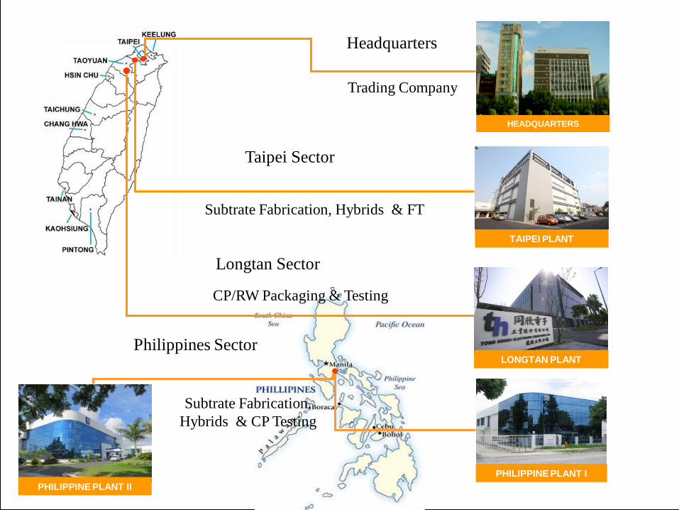
PHILIPPINE PLANT I
HEADQUARTERS
TAIPEI PLANT
Taipei Sector
Philippines Sector
Longtan Sector
Headquarters
PHILIPPINE PLANT II
LONGTAN PLANT
Trading Company
Subtrate Fabrication, Hybrids & FT
CP/RW Packaging & Testing
Subtrate Fabrication,
Hybrids & CP Testing

Tong Hsing Manufacturing Sites
Taipei ChungLi/Longtan Philippine Plant I Philippine Plant II
Address 55 Lane 365, Yingtao
Rd., Yingko District,
New Taipei City, 239
Taiwan
21, Longyuan 5th Rd.,
Longtan Dist.,
Taoyuan City 325,
Taiwan
Lot 15 Road 3
Cermelray Ind’l
Park Canlubang,
Calamba City,
Philippines
103 Prosperity Ave.,
Carmelray Ind’l
Park Canlubang,
Calamba City
Philippines
Established August 1974 April 2015 September 1994 April 2008
Area Land: 138,000 sq. ft. Land: 159,203 sq. ft Land: 80,223 sq. ft. Land : 348,503 sq. ft.
Bldg: 220,000 sq. ft. Bldg: 323,082 sq. ft
Bldg: 47,468 sq. ft. Bldg : 215,547 sq. ft.
Employees: 1148 476 517 950
Quality Certificates ISO 9000
TS 16949
AS 9100 Rev.C
ISO 13485
ISO 14001
OHSAS 18001
China RoHs (Ceramics)
Green Partner
Certified Factory
ISO 9001 ISO/TS16949 ISO 14001 OHSAS 18001 QC080000
ISO 9001:2008 ISO 14001:2004 TS16949:2009 OHSAS 18001:2007 DSCC-VQ-11-023296
Tel: 886-2-2679-0122 886-3-489-3700 63-49-549-2952
63-49-549-2940 Fax: 886-2-2670-0122 886-3-489-3701
Web Site: www.theil.com www.tonghsing.ph

Products and Services
Contract Manufacturing for Microelectronic Packaging and
Ceramic Thick Film/Thin Film Substrate Fabrication.
• RF Modules
• SiP Packaging
• MEMS Packaging
• Image Sensor Packaging
• Reconstruction Wafer
• Circuit Probing and Final Test
• PCB assembly with SMT and/or COB Processes
• Hybrids Assembly
• Thin Film on Alumina and AlN
• Thick Film on Alumina
• DBC on Alumina and AlN

RF Examples
• Application: GPS, PCS, CDMA,
WiMax, WLAN, LTE
• Frequency: 0.8, 0.9, 1.8, 1.9, 2, 3
GHz
• Package type: LGA
• Substrate: PCB substrate
• Process: SMT + D/B + W/B +
Molding + Laser marking + Dicing
• Status: In mass-production
PA Modules Front End Modules MMIC
• Application: GPS, PCS, CDMA,
WiMax, WLAN, LTE
• Frequency: 0.8, 0.9, 1.8, 1.9, 2, 3
GHz
• Package type: LGA
• Substrate: PCB substrate
• Process: SMT + D/B + W/B +
Molding + Laser marking + Dicing
• Status: In mass-production
• Application: Point-to-point radio
application
• Frequency: DC~18G, 10~21G,
20~38G, 34~40G…etc
• Package type: QFN 3X3, 4X4, 5X5,
6X6, 7X7
• Substrate: QFN Leadframe
• Process: D/B + Die Coat (Optional)
+ W/B + Molding + Plating + Dicing
• Status: In mass-production

SiP Examples
• Application: WiFi + BT
• Frequency: 1.6 & 2.4GHz
• Package type: Single side SiP
• Substrate: PCB substrate
• Process: SMT + Flipchip + Underfill + Metal
lid attach + Laser marking + Dicing
• Status: In mass production
• Application: WiFi, GPS, BT, FM, 4 in 1 total
solution
• Frequency: 1.6 & 2.4GHz
• Package type: Single side SiP
• Substrate: PCB substrate
• Process: SMT + Flipchip + Underfill +
Overmold + Pre-dicing + Sputter + Laser
marking +Dicing saw
• Status: In mass-production

Major Strengths
• Flexibility
• Technical Innovation
• Continuous Improvement & Growth
• Excellent High Volume Production Capacity
• Superior Supporting Infrastructure in Northern Taiwan
• Abundant Supply of Human Resources for
Semiconductor Packaging in the Philippines
• Superb Customer Satisfaction
• Strong R & D Partners

SiP is the Trend in Mobile
Phone
Data from Invensas

Various Package for Small Foot
Data from Invensas

Capability of PoP Technologies
Data from Invensas

Basic Concept of BVA
Technology
Top Package
Bottom Package
Two molded packages, Top package and
Bottom package can be electrically
connected together through the vertical
wire bonding
Data from Invensas

Capability of PoP Technologies

Vertical Wire Array

Data from Invensas
Vertical Wire Bonding

Molding

• Exposed Vertical Wire
Molding and Tip Exposure

BVA Reliability

BVA on Memory & MCU

Process Flow for BVA on
Memory & MCU
• The logic substrate has flip chip in the center, and wire-bond pads along the periphery.
• The memory substrate has solder pads along the periphery
• Conventional industry equipment and processes are used to assemble the BVA PoP

BVA SiP Advantages
BVA® Lower Cost
BVA is 3D Vertical Interconnect Technology suitable for
MEMS, RF etc
System-in-Package (SiP) applications
Flexible
Supply
Chain
Vertical integration with existing
wire bond process
Multi-sourcing
Easily scalable supply chain
Fits many active Si and
passives in small footprint Smaller
Footprint
Reliable
Performance Reliable for long life
applications

Example BVA SiP for RF Module
• Additional plane for SMT without interposer
• Reduced parasitic between die to passives
• Shorter interconnect between die
• 40% reduction in SiP component footprint
40% area
reduction

Example BVA for Image Sensor

Summary
• BVA technology is invented and developed by Invensas. This novel
technology can offer higher I/O and high aspect ratio interconnection for
PoP module.
• The vertical wire technology has been applied to Fan-out process for
interconnection in Tong Hsing. We used it for several image sensor
package development.
• In additional to the OEM service, Tong Hsing develop suitable package
method and work with customer to verify the advanced package
approach for future requirement.


![[Array, Array, Array, Array, Array, Array, Array, Array, Array, Array, Array, Array]](https://static.fdocuments.in/doc/165x107/56816460550346895dd63b8b/array-array-array-array-array-array-array-array-array-array-array.jpg)

![Arte pop [pop art]](https://static.fdocuments.in/doc/165x107/558d408ad8b42aa44f8b4706/arte-pop-pop-art.jpg)