Bulk Material Micro-structuring and Surface Modifications · Bulk Material Micro-structuring and...
58
© IMM, 2007 www.holger-loewe.de Bulk Material Micro-structuring and Surface Modifications irradiation electrodeposition polymer coatings mechanical PVD/CVD SAMs electrochemical chemical electrical (EDM) polymers semiconductors glass ceramics metals Micro-structuring Materials Surface modification chemical
Transcript of Bulk Material Micro-structuring and Surface Modifications · Bulk Material Micro-structuring and...
© IMM, 2007www.holger-loewe.de
Bulk Material Micro-structuring and Surface Modifications
irradiation
electrodeposition
polymer coatings
mechanical
PVD/CVD
SAMs
electrochemical
chemical
electrical (EDM)
polymers
semiconductors
glass
ceramics
metals
Micro-structuring
Materials
Surface modification
chemical

© IMM, 2007www.holger-loewe.de
Principle of Optical Lithography
mask
negative
UV-exposure
of resist
development
result
© IMM, 2007www.holger-loewe.de
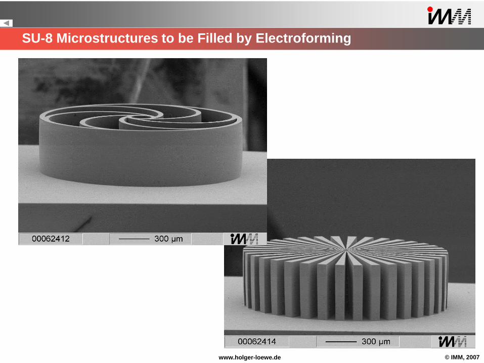
SU-8 Microstructures to be Filled by Electroforming
© IMM, 2007www.holger-loewe.de
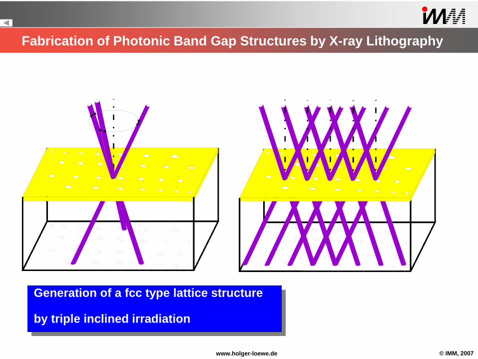
Fabrication of Photonic Band Gap Structures by X-ray Lithography
Generation of a fcc type lattice structure
by triple inclined irradiation

© IMM, 2007www.holger-loewe.de
100 µm
100 µm
Made by LiGA - technique
3-D Microstructures in PMMA
© IMM, 2007www.holger-loewe.de
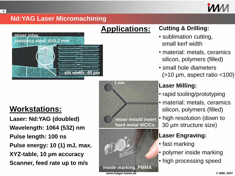
Nd:YAG Laser Micromachining
Workstations:
Laser: Nd:YAG (doubled)
Wavelength: 1064 (532) nm
Pulse length: 100 ns
Pulse energy: 10 (1) mJ, max.
XYZ-table, 10 µm accuracy
Scanner, feed rate up to m/s
Applications: Cutting & Drilling:
• sublimation cutting,
small kerf width
• material: metals, ceramics
silicon, polymers (filled)
• small hole diameters
(>10 µm, aspect ratio <100)
mixer inlay,
stainless steel, d=0.2 mm
slit width: 40 µm
Laser Milling:
• rapid tooling/prototyping
• material: metals, ceramics
silicon, polymers (filled)
• high resolution (down to
30 µm structure size)mixer mould insert
hard metal WC/Co
1 mm
Laser Engraving:
• fast marking
• polymer inside marking
• high processing speedinside marking, PMMA

© IMM, 2007www.holger-loewe.de
Eximer Laser Micromachining
EXITEC-Workstation:
Laser: Excimer LPX110i
Wavelength: 193 nm
Pulse length: 17 ns
Pulse energy: 200 mJ (max.)
XYZ-table, 1 µm accuracy
Mask projection
Applications:
1 mm
Polymer Machining:
• ablation (depth 5 µm to
1 mm, resolution <5 µm
Ra>0.2 µm, quasi 3D)
• fine cutting
• drilling (various hole
shapes)
cutting of PI foil
caterpillar mixer,
PMMA prototype
Rapid Prototyping:
• microfluidic channels
• polymer bio chips
• microoptical structures
Laser LIGA:
• mould insert fabrication
• material: Ni, Cu
• large number production
(hot embossing, injec-
tion moulding)
Ni mould insert
hydrofocussing chip
0.3 mm
© IMM, 2007www.holger-loewe.de
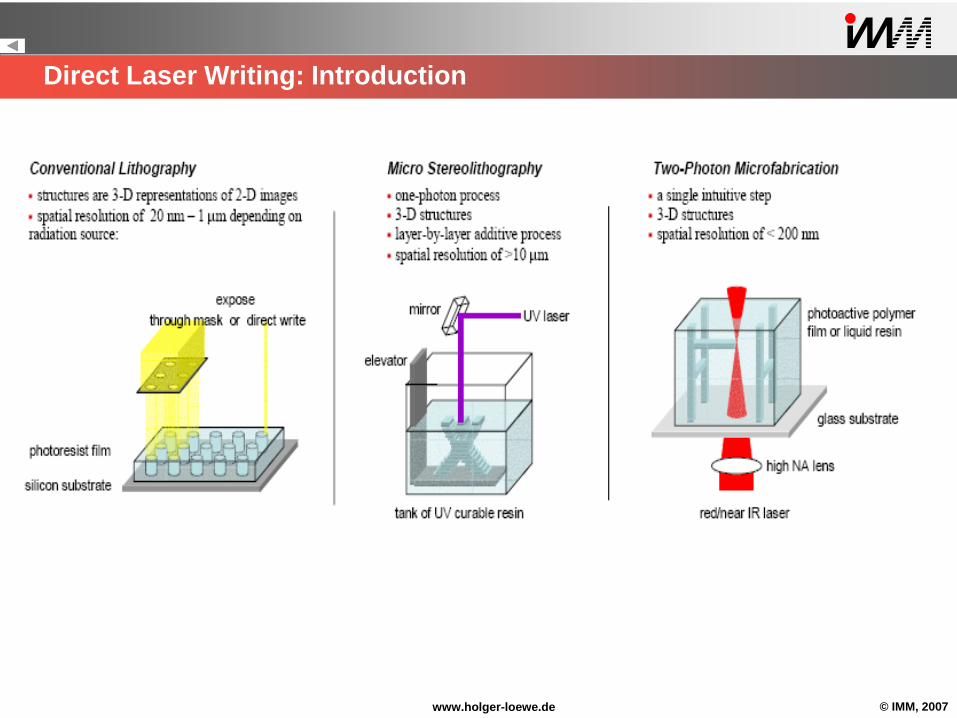
Direct Laser Writing: Introduction

© IMM, 2007www.holger-loewe.de
Direct Laser Writing: Experimental Setup
Scanneroptics
Pumplaser
(532 nm, 5 W)
Autocorrelator
Spectrometer
Shutter
PC
Microscope objective
Ti:Saphir
Oscillator
(800 nm, 400 mW)
xyz-Table
z-Piezoactor

© IMM, 2007www.holger-loewe.de
Interference Lithography: Working Principle
If two (or more) coherent laser beams overlap in space, an interference pattern with distinct bright and dark regions is generated.
Idea: Expose a photosensitive polymer layer (photoresist) with this pattern.

© IMM, 2007www.holger-loewe.de
Interference Lithography: Simulation
The pattern geometry is determined by the number of laser beams and their respective intensity, orientation, and polarization.

© IMM, 2007www.holger-loewe.de
Direct Laser Writing: Wood-Pile Structures
Application: Photonic Crystals
with complete band-gap
Resist: SU-8

© IMM, 2007www.holger-loewe.de
Direct Laser Writing: Results
1D Voxel 2D Lines 3D Bodies
vv
0 5 10 15 20 25 30 350
200
400
600
800
19 mW
12 mW
10 mW
7 mW
str
uctu
re h
eig
ht
[nm
]
exposure time [ms]
0 5 10 15 20 25 30 35 40 45
0,4
0,6
0,8
1,0
1,2
1,4
1,6
1,8
2,0
2,2
19 mW
12 mW
10 mW
7 mW
str
uctu
re w
idth
[µ
m]
exposure time [ms]

© IMM, 2007www.holger-loewe.de
Interference Lithography: 2-D Structures
The actual pattern obtained also depends on the properties of the photoresist material.
© IMM, 2007www.holger-loewe.de HP 64174
AFM image
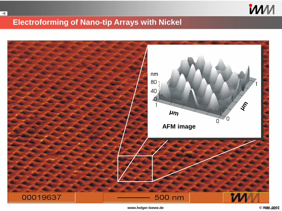
Electroforming of Nano-tip Arrays with Nickel
© IMM, 2007www.holger-loewe.de
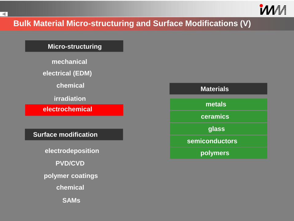
Bulk Material Micro-structuring and Surface Modifications (V)
irradiation
electrodeposition
polymer coatings
mechanical
PVD/CVD
SAMs
electrochemical
chemical
electrical (EDM)
polymers
semiconductors
glass
ceramics
metals
Micro-structuring
Materials
Surface modification
chemical

© IMM, 2007www.holger-loewe.de
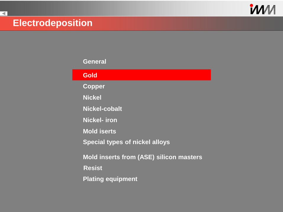
Electrodeposition
Special types of nickel alloys
Nickel
Mold iserts
Nickel- iron
Nickel-cobalt
Mold inserts from (ASE) silicon masters
Copper
General
Resist
Plating equipment
Gold
© IMM, 2007www.holger-loewe.de
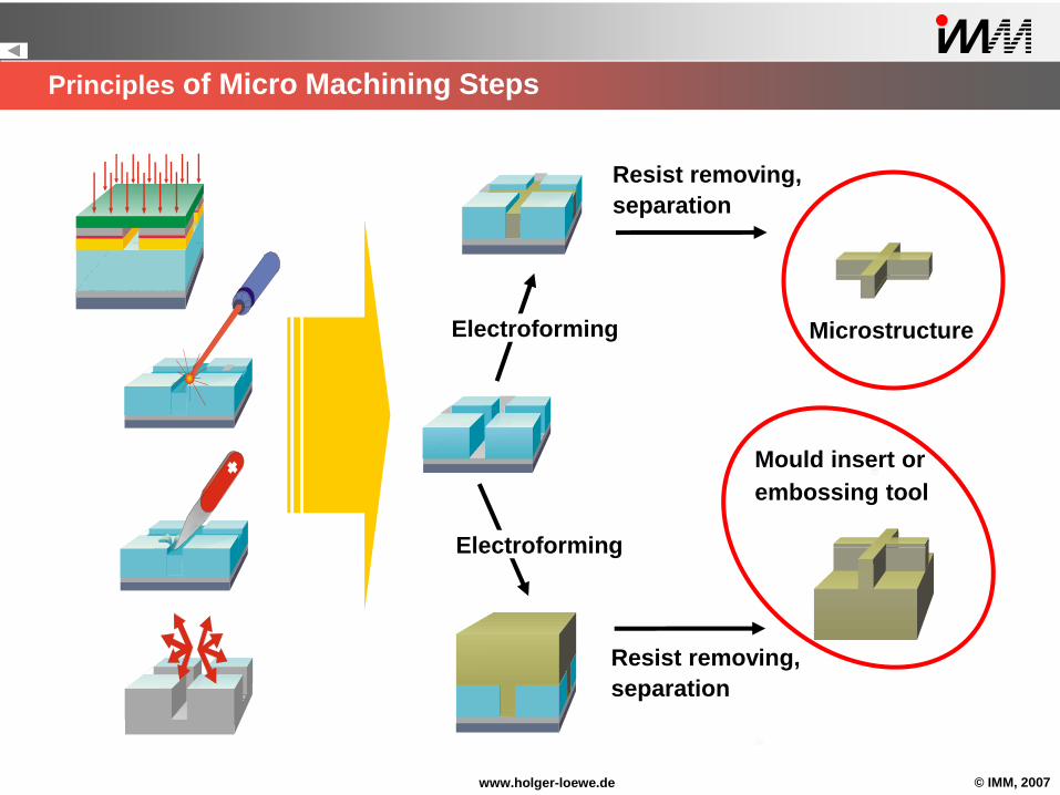
Principles of Micro Machining Steps
Microstructure
Resist removing,
separation
Electroforming
Mould insert or
embossing tool
Arbeitsmaske
Electroforming
Resist removing,
separation

© IMM, 2007www.holger-loewe.de
Main Problems in Microelectroforming
2. Adhesion
1. Metal distribution
3. Particels and bubbles
4. Undercutting
5. Internal stress
pressure tensile
Plating base
Resist
Metal

© IMM, 2007www.holger-loewe.de
Typical Defects Caused by Electroplating of fully metalized ASE-etched Si-surfaces
Sputtered adhesion
and seed layer
Sputtered adhesion
and seed layer
Deposited nickel
Deposited nickel
Electrolyte entrapment
ASE-etched Si-masterAspect ratio 2:1
Growing direction
ASE-etched Si-master
Electrolyte
Aspect ratio 1:1
© IMM, 2007www.holger-loewe.de
Electrodeposition
Special types of nickel alloys
Nickel
Mold iserts
Nickel- iron
Nickel-cobalt
Mold inserts from (ASE) silicon masters
Copper
General
Resist
Plating equipment
Gold
© IMM, 2007www.holger-loewe.de
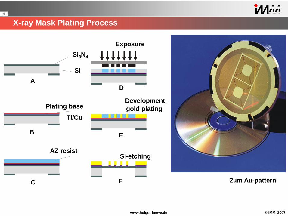
X-ray Mask Plating Process
Si
Si3N4
Plating base
AZ resist
A
B
C
Exposure
Development,
gold plating
Si-etching
D
E
F
Ti/Cu
2µm Au-pattern

© IMM, 2007www.holger-loewe.de
Electrodeposition of Gold: Working Conditions
Gold electrolyte
Gold content
Sulfite as sodium sulfite
pH - value
Temperature
Current density
Anode material
Leveler
Modified commercial available
gold sulfite electrolyte
8 - 12 g/l
40 g/l
Arsenite / arsenate
9.3 - 9.6
55° C
0.2 - 0.4 A/dm²
Ti/Pt mesh
© IMM, 2007www.holger-loewe.de
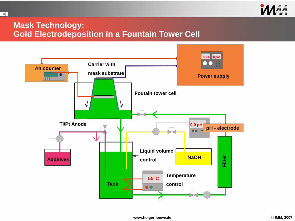
Mask Technology:Gold Electrodeposition in a Fountain Tower Cell
Power supply
Additives
Tank
Liquid volume
control
Temperature
control
Carrier with
mask substrateAh counter
NaOH
Foutain tower cell
Ti/Pt AnodepH - electrode
Filte
r
55°C
9.0 pH
0,5V0,5V0,2A
© IMM, 2007www.holger-loewe.de
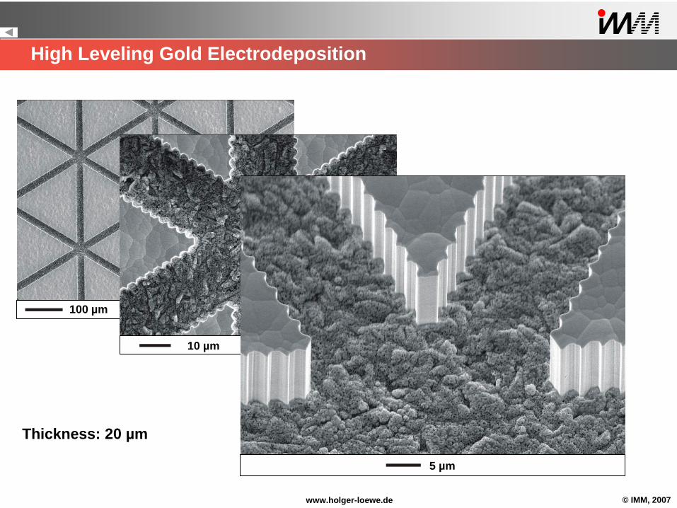
High Leveling Gold Electrodeposition
Thickness: 20 µm
100 µm
10 µm
5 µm

© IMM, 2007www.holger-loewe.de
Mistakes in Electroplating of Gold - Leveler Concentration Too Low
61991

© IMM, 2007www.holger-loewe.de
Deep X-ray Lithography: Substrate Induced Defects
Formation of gas bubbles by
dissolution of the Be-substrate
during the electrodeposition process
Be + 2 H2O Be(OH)2 + H2
Be
Be
Au
Au

© IMM, 2007www.holger-loewe.de
Electroplating with AFM Tips: Gold Nanoelectrodes
Electrode gap
© IMM, 2007www.holger-loewe.de
Electrodeposition
Special types of nickel alloys
Nickel
Mold iserts
Nickel- iron
Nickel-cobalt
Mold inserts from (ASE) silicon masters
Copper
General
Resist
Plating equipment
Gold
© IMM, 2007www.holger-loewe.de
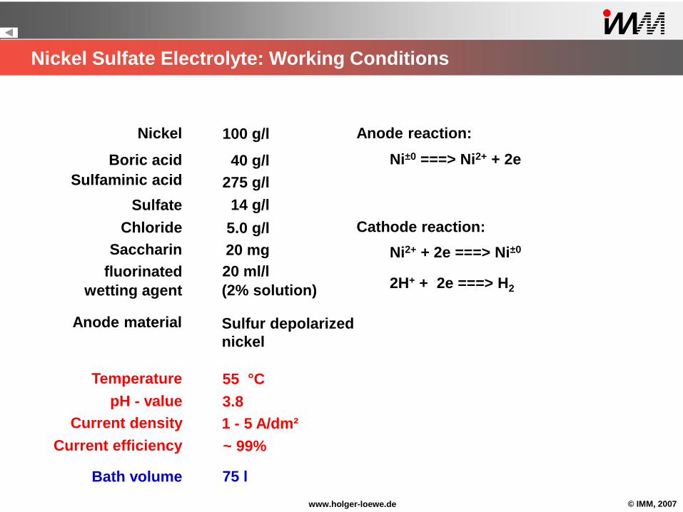
Nickel
Boric acid
Sulfaminic acid
Sulfate
Chloride
100 g/l
40 g/l
275 g/l
14 g/l
5.0 g/l
Temperature
pH - value
Current density
fluorinated
wetting agent
55 °C
3.8
1 - 5 A/dm²
Bath volume 75 l
20 ml/l
(2% solution)
Current efficiency ~ 99%
Anode reaction:
Ni±0 ===> Ni2+ + 2e
Cathode reaction:
Ni2+ + 2e ===> Ni±0
2H+ + 2e ===> H2
Saccharin 20 mg
Anode material Sulfur depolarized
nickel
Nickel Sulfate Electrolyte: Working Conditions

© IMM, 2007www.holger-loewe.de
3.3 pH
Additives
Tank
Liquid level
control
Temperature
control
Wafer carrier
Ah counter
Sulfamic acid
Dummy plating
Cell
Filte
r
55°C
Ni-
an
od
e
Power supply
1,5A 3,8V 0,2A 0,5V
pH-electrode
Nickel Electrodeposition: Flow Chart
© IMM, 2007www.holger-loewe.de
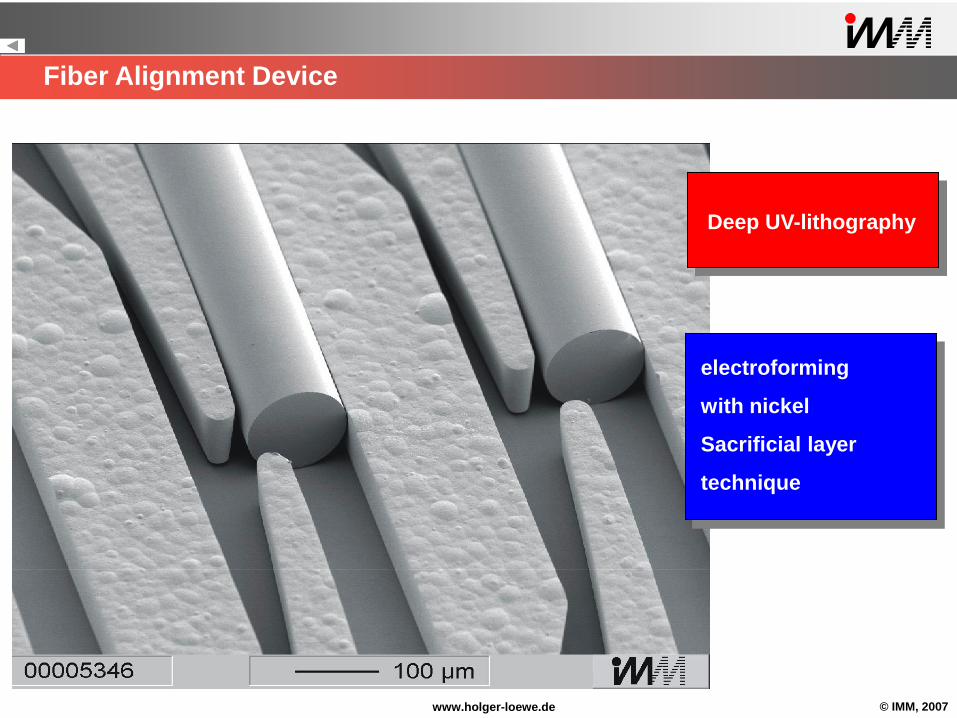
Fiber Alignment Device
electroforming
with nickel
Sacrificial layer
technique
Deep UV-lithography
© IMM, 2007www.holger-loewe.de
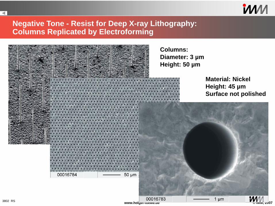
Negative Tone - Resist for Deep X-ray Lithography:Columns Replicated by Electroforming
3802 RS
Columns:
Diameter: 3 µm
Height: 50 µm
Material: Nickel
Height: 45 µm
Surface not polished

© IMM, 2007www.holger-loewe.de
LIGA - Microstructures Made from Nickel: Oblique X-ray Irradiation
© IMM, 2007www.holger-loewe.de
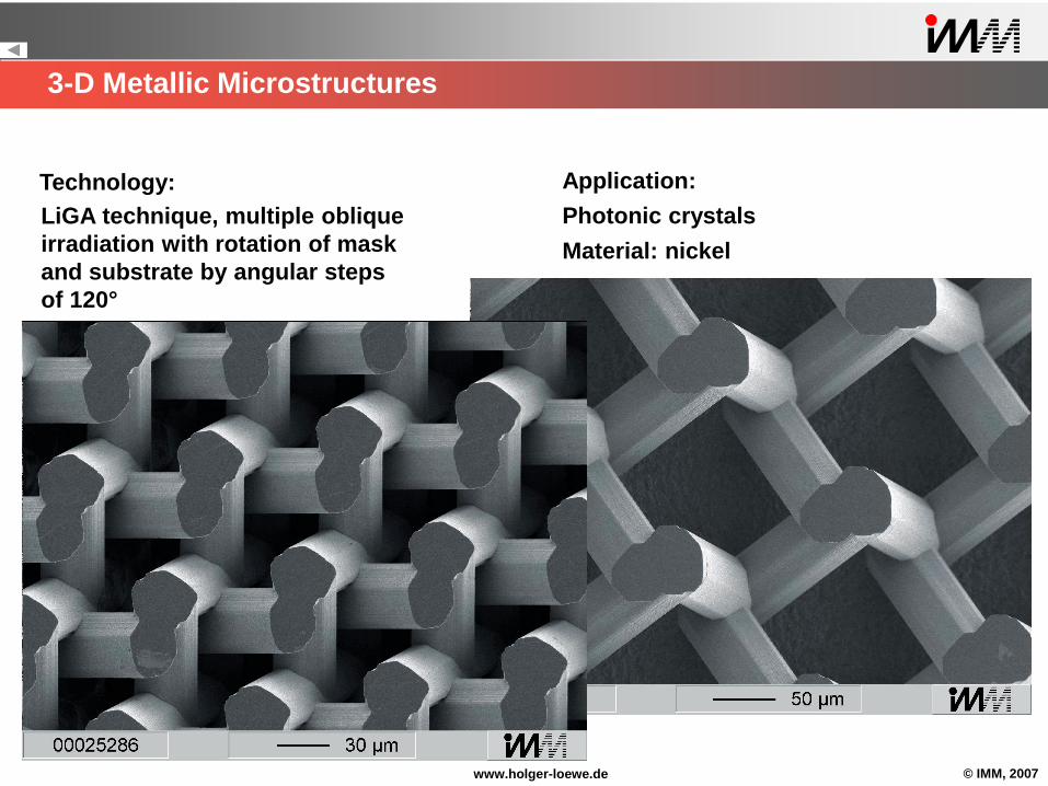
3-D Metallic Microstructures
Technology:
LiGA technique, multiple oblique
irradiation with rotation of mask
and substrate by angular steps
of 120°
Application:
Photonic crystals
Material: nickel

© IMM, 2007www.holger-loewe.de
Young´s Modulus of Nickel Microstructures
0 200 400 600 800 1000 1200
100
60
140
180
220
Annealing temperature [°C]
Dimension of the test piece:
2800 µm * 100 µm * 400 µm
( S. Abel; PhD thesis, unpublished results )
Mo
du
lus o
f ela
sti
cit
y [
GP
a]
© IMM, 2007www.holger-loewe.de
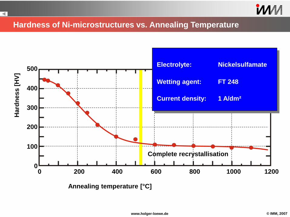
Hardness of Ni-microstructures vs. Annealing Temperature
0 200 400 600 800 1000 12000
100
200
300
400
500
Annealing temperature [°C]
Electrolyte: Nickelsulfamate
Wetting agent: FT 248
Current density: 1 A/dm²
Complete recrystallisation
Hard
ness [
HV
]
© IMM, 2007www.holger-loewe.de
Electrodeposition
Special types of nickel alloys
Nickel
Mold iserts
Nickel- iron
Nickel-cobalt
Mold inserts from (ASE) silicon masters
Copper
General
Resist
Plating equipment
Gold
© IMM, 2007www.holger-loewe.de
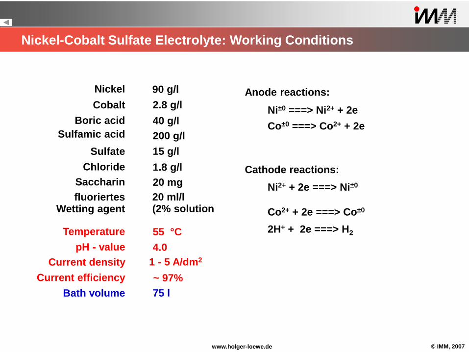
Nickel
Boric acid
Sulfamic acid
Sulfate
Chloride
90 g/l
40 g/l
200 g/l
15 g/l
1.8 g/l
Temperature
pH - value
Current density
fluoriertesWetting agent
55 °C
4.0
Bath volume 75 l
20 ml/l(2% solution
Current efficiency ~ 97%
Anode reactions:
Ni±0 ===> Ni2+ + 2e
Cathode reactions:
Ni2+ + 2e ===> Ni±0
2H+ + 2e ===> H2
Cobalt 2.8 g/l
Co±0 ===> Co2+ + 2e
Co2+ + 2e ===> Co±0
Saccharin 20 mg
1 - 5 A/dm2
Nickel-Cobalt Sulfate Electrolyte: Working Conditions
© IMM, 2007www.holger-loewe.de
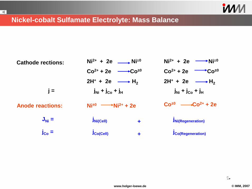
Cathode rections:
Cell Regeneration
j = jNi + jCo + jH jNi + jCo + jH
Ni2+ + 2e Ni0
2H+ + 2e H2
Co2+ + 2e Co±0
Anode reactions: Ni±0 Ni2+ + 2e
Ni2+ + 2e Ni0
Co2+ + 2e Co±0
2H+ + 2e H2
Co±0 Co2+ + 2e
JNi = jNi(Cell) jNi(Regeneration)+
jCo = jCo(Cell) jCo(Regeneration)+
Nickel-cobalt Sulfamate Electrolyte: Mass Balance

© IMM, 2007www.holger-loewe.de
3.3 pH
Tank
Liquid level
control
Temperatur
control
Carrier with
wafer
Sulfamic acidAdditives
Cell
Regeneration
Ah counter
Power supply
1,5A 3,8V 0,2A 0,5V
pH-electrode
VIS-photometer
55°C
Filte
r
Ni-
an
od
e
Co
-an
od
e
Ni-Co Alloy Electrodeposition: Flow Chart

© IMM, 2007www.holger-loewe.de
Cobalt content in the
deposit versus cobalt
concentration in the
electrolyte
pH 4.0
T 55°C
Nickel 90 g/l
Sodium sulfamate 40 g/l
Sodium sulfate 15 g/l
Chloride 1.8 g/l
0 2 4 6 8 10
Cobalt content in the electrolyte [ g/l ]
Co
balt
co
nte
nt
in t
he d
ep
osit
[%
]
10
20
30
40
50
Electroplating of Ni-Co Microstructures
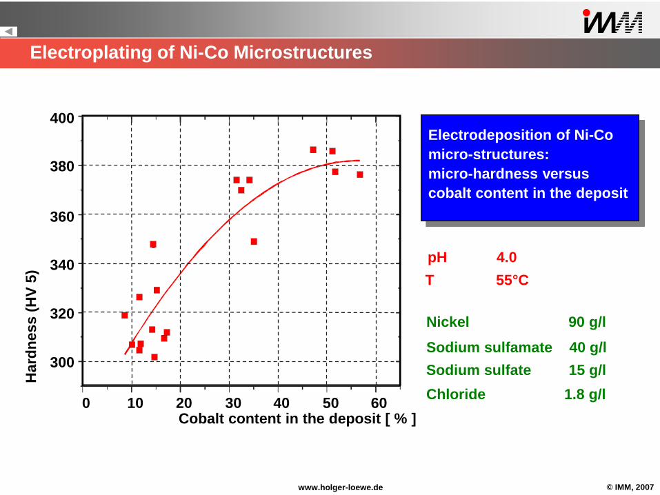
© IMM, 2007www.holger-loewe.de
pH 4.0
T 55°C
0 10
Electrodeposition of Ni-Co
micro-structures:
micro-hardness versus
cobalt content in the deposit
20 30 40 50 60Cobalt content in the deposit [ % ]
400
380
360
340
320
300
Nickel 90 g/l
Sodium sulfamate 40 g/l
Sodium sulfate 15 g/l
Chloride 1.8 g/l
Hard
ness (
HV
5)
Electroplating of Ni-Co Microstructures

© IMM, 2007www.holger-loewe.de
Electroforming of Mould Inserts
Material: Ni-Co alloy
© IMM, 2007www.holger-loewe.de
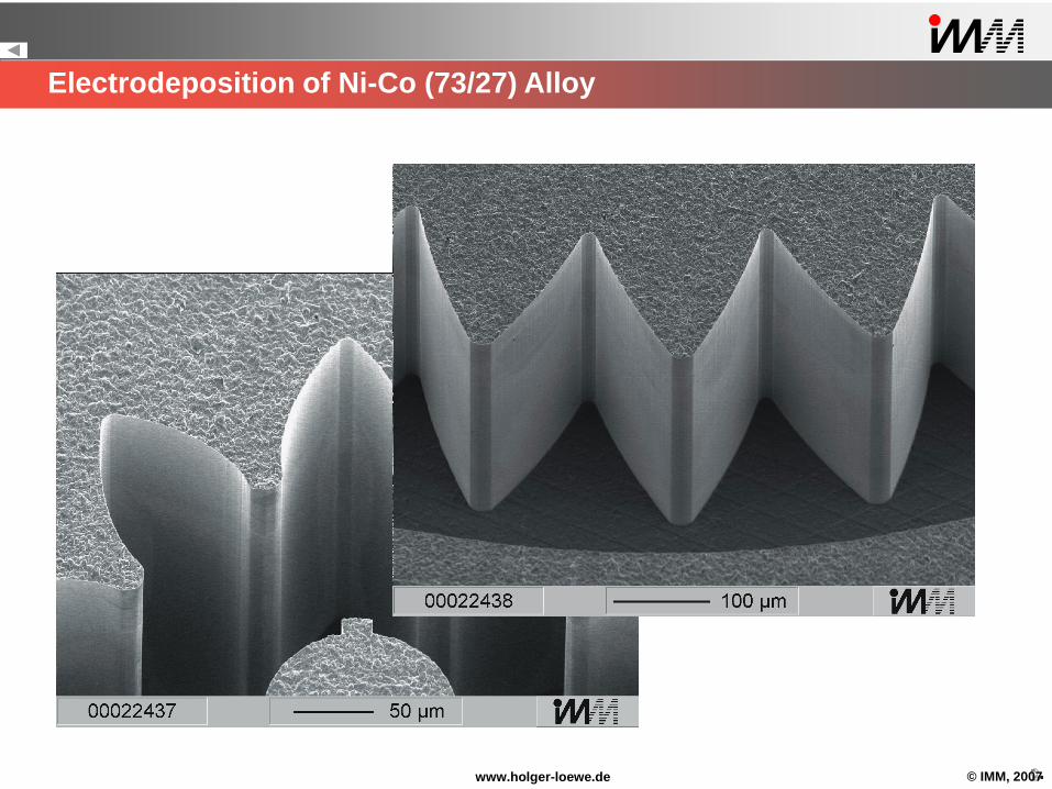
Electrodeposition of Ni-Co (73/27) Alloy
Micro gears manufacturedby LIGA-technology
© IMM, 2007www.holger-loewe.de
Electrodeposition
Special types of nickel alloys
Nickel
Mold iserts
Nickel- iron
Nickel-cobalt
Mold inserts from (ASE) silicon masters
Copper
General
Resist
Plating equipment
Gold

© IMM, 2007www.holger-loewe.de
Nickel-Iron Alloy Electrodeposition: Working Conditions
Nickel
Boric acid
Sulfate
Complexing agent
Chloride
50 g/l
45 g/l
80 g/l
15 g/l
18 g/l
Temperature
pH - value
Current density
Tenside
55 °C
3.5
1 - 5 A/dm²
Volume 50 l
5 ml/l
(2% Lösung)
Current efficiency ~ 98%
Anode reaction:
Ni±0 ===> Ni2+ + 2e
Cathode reaction:
Ni2+ + 2e ===> Ni±0
2H+ + 2e ===> H2
Iron 1-9 g/l
Fe±0 ===> Fe2+ + 2e
2Fe3+ + Fe±0 ===> 3Fe2+
Fe2+ ===> Fe3+ + 1e
Fe2+ + Oxygen in air ===> Fe3+
Fe2+ + 2e ===> Fe±0
Saccharin 20 mg
Side reaction:

© IMM, 2007www.holger-loewe.de
3.3 pH
Power supply
Tank
Liquid level
control
Temperature
control
Sulfuric-acid
pH-Electrode
Potentiostat
Additives
55°C
Cell
Dummy
plating
Ah -counter
Ni-
an
od
e
Ni-
an
od
ePC
Fe
-an
od
e
PC
VIS-photometer
Filte
r
1,5A 3,8V0,5V
0,5V0,2A
Nickel-Iron Alloy Electrodeposition: Flow Chart

© IMM, 2007www.holger-loewe.de
Cathodic reactions:
Cell Regeneration cell
j = jNi + jFe + jH jNi + jFe + jH
Ni2+ + 2e Ni0
2H+ + 2e H2
Fe2+ + 2e Fe±0
Fe±0 Fe2+ + 2e
Anodic reactions Ni±0 Ni2+ + 2e
2Fe2+ + Fe±0 3Fe2+
Fe2+ + oxygen in air Fe3+Side reactions:
Ni2+ + 2e Ni0
Fe2+ + 2e Fe±0
2H+ + 2e H2
Ni±0 Ni2+ + 2e
Nickel-iron Sulfamate Electrolyte: Mass Balance

© IMM, 2007www.holger-loewe.de
Nickel
Ni-Fe (50:50)
- 40000 - 20000 0 20000 40000
-1,5
-1,0
-0,5
0
0,5
1,0
1,5
SA 3004
Magnetic field H [ A/m ]
Satu
rati
on
mag
neti
zati
on
[ T
]Comparison of Nickel and Nickel-Iron Microstructures: Hysteresis Curves

© IMM, 2007www.holger-loewe.de
Material For Leaf-Springs; Electroplated Ni-Fe (90/10) Alloy

© IMM, 2007www.holger-loewe.de
Endurance Strength of Ni-Fe Alloy Microstructures
0 20 40 60104
106
108
Iron content [%]
Bre
akin
g l
oad
cycle
20,000,000 cycles
© IMM, 2007www.holger-loewe.de
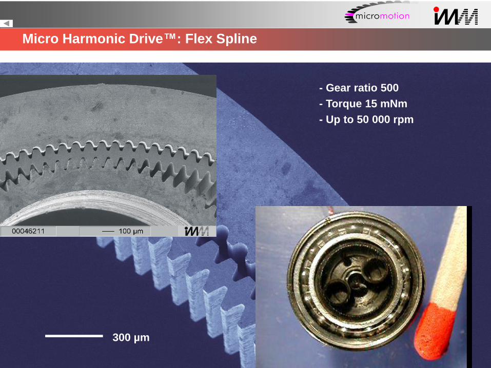
Micro Harmonic Drive™: Flex Spline
300 µm
- Gear ratio 500
- Torque 15 mNm
- Up to 50 000 rpm
© IMM, 2007www.holger-loewe.de
Electrodeposition
Special types of nickel alloys
Nickel
Mold iserts
Nickel- iron
Nickel-cobalt
Mold inserts from (ASE) silicon masters
Copper
Resist
Plating equipment
Gold

© IMM, 2007www.holger-loewe.de
Nickel Mold Insert for Lab-On-A-Chip Fabrication
Delay loopReservoirs 2
Reactand dosing
Reservoirs 1
Iso 90402
Separation channel
© IMM, 2007www.holger-loewe.de
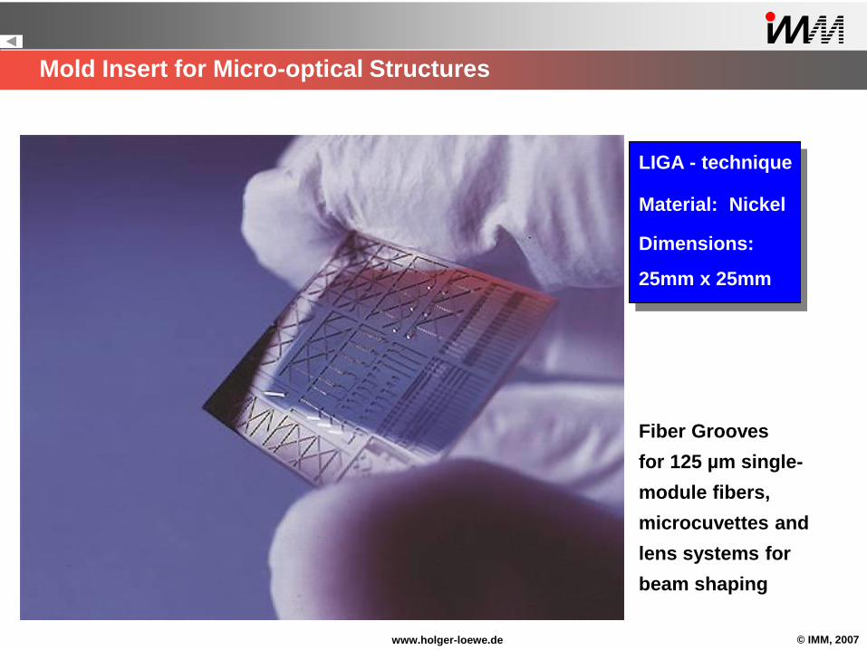
Mold Insert for Micro-optical Structures
Material: Nickel
LIGA - technique
Dimensions:
25mm x 25mm
Fiber Grooves
for 125 µm single-
module fibers,
microcuvettes and
lens systems for
beam shaping
© IMM, 2007www.holger-loewe.de
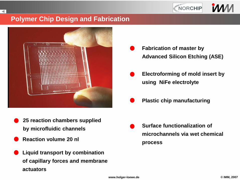
Polymer Chip Design and Fabrication
Fabrication of master by
Advanced Silicon Etching (ASE)
Surface functionalization of
microchannels via wet chemical
process
25 reaction chambers supplied
by microfluidic channels
Liquid transport by combination
of capillary forces and membrane
actuators
Reaction volume 20 nl
Electroforming of mold insert by
using NiFe electrolyte
Plastic chip manufacturing

© IMM, 2007www.holger-loewe.de
Ultraprecision Hot Embossing
63018
Resist master
Glass base
Metallisation
Electrolyticreinforcement
Embossing tool
PC-foil
Sensorcomponent
Minimum feature size: <3nm
Reproducibility: <1nm