Buffer Design and Assignment for Structured ASIC · PDF fileBuffer Design and Assignment for...
18
JOURNAL OF INFORMATION SCIENCE AND ENGINEERING 30, 107-124 (2014) 107 Buffer Design and Assignment for Structured ASIC * PO-YANG HSU AND YI-YU LIU Department of Computer Science and Engineering Yuan Ze University Chungli, 320 Taiwan In modern VLSI design, interconnection delay dominates the circuit delay due to its heavy downstream capacitance. Buffer insertion is a widely used technique for splitting a long wire into several buffered wire segments for circuit performance improvement. In this paper, we investigate buffer insertion issues in structured ASIC design style. We de- sign the layout for two dedicated buffers and extract the technology-dependent parame- ters for evaluation. Furthermore, we propose post-routing channel migration techniques, which employ intra-channel migration and inter-channel migration, to deal with the sub-channel saturation problem during buffer assignment. Compared to the baseline de- signs with 4X-buffer at the CLB output, our proposed structured ASIC design and opti- mization techniques improve the circuit performance by 65.7% and the ratio of wire de- lay to gate delay from 8.2 to 0.8. Keywords: structured ASIC, via patterned gate array, buffer assignment, channel migra- tion, timing optimization 1. INTRODUCTION In the deep sub-micron era, mask cost has increased dramatically due to lithographic difficulties. The one-time-use mask is no longer affordable for small-volume ASIC designs. This results in a high-cost threshold for conventional standard cell ASIC designs. To amortize mask cost, some pre-fabricated design styles have been proposed. Those design styles provide different levels of pre-fabrication: device level, gate level, semi- chip level, and full-chip level. Among them, structured ASIC is a semi-chip level pre- fabricated design style. Most of the masks are fixed except the contact mask and some via masks. The functionalities and the interconnections are specified by properly assign- ing the contacts and the vias. It is also known as the via patterned gate array (VPGA)s [1-7]. With low non-recurring engineering (NRE) costs and medium circuit perfor- mance compared with the conventional standard cell design, structured ASIC provides a new alternative for circuit designers in terms of the mask cost, programmability, and per- formance. Since interconnection delay dominates circuit delay in modern VLSI design, buffer insertion becomes an important technique. The interconnection delay results from the parasitic resistance and capacitance on a wire. Since downstream capacitance can be greatly reduced by buffer insertion, the interconnection delay can be reduced at the ex- pense of extra buffer area. Van Ginnecken exploits the special properties of Elmore delay model and proposes a dynamic-programming based algorithm for buffer assignment [8]. Gao and Wong optimally solve the buffer planning problem by using a graph-based al- Received October 8, 2011; revised March 5, 2012 & May 7, 2012; accepted May 20, 2012. Recommended by Yao-Wen Chang. * This work was supported in part by the National Science Council of Taiwan, under Grants NSC-96-2221-E- 155-070 and NSC-97-2221-E-155-071-MY2.
Transcript of Buffer Design and Assignment for Structured ASIC · PDF fileBuffer Design and Assignment for...
JOURNAL OF INFORMATION SCIENCE AND ENGINEERING 30, 107-124 (2014)
107
Buffer Design and Assignment for Structured ASIC*
PO-YANG HSU AND YI-YU LIU
Department of Computer Science and Engineering Yuan Ze University
Chungli, 320 Taiwan
In modern VLSI design, interconnection delay dominates the circuit delay due to its
heavy downstream capacitance. Buffer insertion is a widely used technique for splitting a long wire into several buffered wire segments for circuit performance improvement. In this paper, we investigate buffer insertion issues in structured ASIC design style. We de-sign the layout for two dedicated buffers and extract the technology-dependent parame-ters for evaluation. Furthermore, we propose post-routing channel migration techniques, which employ intra-channel migration and inter-channel migration, to deal with the sub-channel saturation problem during buffer assignment. Compared to the baseline de-signs with 4X-buffer at the CLB output, our proposed structured ASIC design and opti-mization techniques improve the circuit performance by 65.7% and the ratio of wire de-lay to gate delay from 8.2 to 0.8. Keywords: structured ASIC, via patterned gate array, buffer assignment, channel migra-tion, timing optimization
1. INTRODUCTION
In the deep sub-micron era, mask cost has increased dramatically due to lithographic difficulties. The one-time-use mask is no longer affordable for small-volume ASIC designs. This results in a high-cost threshold for conventional standard cell ASIC designs. To amortize mask cost, some pre-fabricated design styles have been proposed. Those design styles provide different levels of pre-fabrication: device level, gate level, semi- chip level, and full-chip level. Among them, structured ASIC is a semi-chip level pre- fabricated design style. Most of the masks are fixed except the contact mask and some via masks. The functionalities and the interconnections are specified by properly assign- ing the contacts and the vias. It is also known as the via patterned gate array (VPGA)s [1-7]. With low non-recurring engineering (NRE) costs and medium circuit perfor- mance compared with the conventional standard cell design, structured ASIC provides a new alternative for circuit designers in terms of the mask cost, programmability, and per- formance.
Since interconnection delay dominates circuit delay in modern VLSI design, buffer insertion becomes an important technique. The interconnection delay results from the parasitic resistance and capacitance on a wire. Since downstream capacitance can be greatly reduced by buffer insertion, the interconnection delay can be reduced at the ex-pense of extra buffer area. Van Ginnecken exploits the special properties of Elmore delay model and proposes a dynamic-programming based algorithm for buffer assignment [8]. Gao and Wong optimally solve the buffer planning problem by using a graph-based al-
Received October 8, 2011; revised March 5, 2012 & May 7, 2012; accepted May 20, 2012. Recommended by Yao-Wen Chang. * This work was supported in part by the National Science Council of Taiwan, under Grants NSC-96-2221-E-
155-070 and NSC-97-2221-E-155-071-MY2.
PO-YANG HSU AND YI-YU LIU
108
gorithm [9]. In the standard cell design style, there are a set of buffers in a cell library. CAD tools select the potential critical paths and place buffers on those paths. Post-layout buffer insertion can be done by slightly modifying the placement and routing results. In the FPGA design style, plenty of switch buffers reside in the switch blocks. These switch buffers explicitly cut off the downstream capacitance at the cost of fairly large gate delay overheads. In the structured ASIC design style, the downstream capacitance would be-come a crucial problem because neither different driving-strength gates nor switch buff-ers could be used. To solve this problem, dedicated pre-fabricated buffers may be a solu-tion. The aforementioned issues motivate us to design dedicated buffers for the intercon-nections. We design the layouts of two dedicated buffers and extract the technology de-pendent parameters for evaluations. In addition, buffer assignment and channel migration algorithms are proposed for timing optimization.
The rest of this paper is organized as follows. The preliminary background knowl-edge and the motivation of this paper are given in Section 2. Section 3 presents the layout of our buffered structured ASIC and buffer assignment algorithm. Section 4 illustrates our channel migration algorithm. The experimental results are drawn in Section 5. Sec-tion 6 concludes this paper.
2. MOTIVATION
In this section, we give the background of island-style FPGAs followed by island- style structured ASICs. After that, we address the buffer insertion issues for structured ASIC design.
2.1 Island-style FPGA
Island-style FPGA architecture is a well-known chip level pre-fabricated design
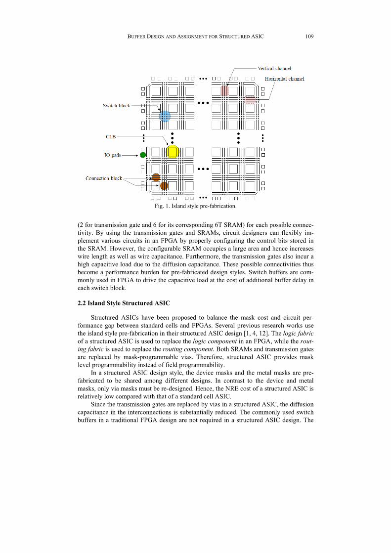
style [10, 11]. There are two major components in an island-style pre-fabrication, logic component and routing component. The logic component is composed of configurable logic blocks (CLB). Each CLB contains a set of basic logic elements (BLE) to realize both combinational and sequential logic functions. Moreover, the routing component consists of routing channels, connection blocks, and switch blocks. The routing channels are made up of several routing tracks. The connection blocks are used to determine the connectivities between the I/O of CLB and the routing tracks. The switch blocks are used to determine the connectivities between different routing tracks in different routing channels. Therefore, with tracks, connection blocks, and switch blocks, routing compo-nents are capable of interconnecting logic components. Fig. 1 briefly illustrates island- style prefabrication.
A LUT-based FPGA is a representative of island style pre-fabrication. The field programmability of FPGA is based on both the SRAMs and the transmission gates. In a logic component, the truth table in a LUT can be stored in the SRAM to realize different combinational and sequential logic functions. In a routing component, an electric switch is necessary for implementing each possible connectivity. The electric switch can be re-alized by using either transmission gates or pass transistors. Additionally, the control signal of electric switch can be stored in an SRAM. Hence, we need at least 8 transistors
BUFFER DESIGN AND ASSIGNMENT FOR STRUCTURED ASIC
109
Fig. 1. Island style pre-fabrication.
(2 for transmission gate and 6 for its corresponding 6T SRAM) for each possible connec-tivity. By using the transmission gates and SRAMs, circuit designers can flexibly im-plement various circuits in an FPGA by properly configuring the control bits stored in the SRAM. However, the configurable SRAM occupies a large area and hence increases wire length as well as wire capacitance. Furthermore, the transmission gates also incur a high capacitive load due to the diffusion capacitance. These possible connectivities thus become a performance burden for pre-fabricated design styles. Switch buffers are com-monly used in FPGA to drive the capacitive load at the cost of additional buffer delay in each switch block.
2.2 Island Style Structured ASIC
Structured ASICs have been proposed to balance the mask cost and circuit per-
formance gap between standard cells and FPGAs. Several previous research works use the island style pre-fabrication in their structured ASIC design [1, 4, 12]. The logic fabric of a structured ASIC is used to replace the logic component in an FPGA, while the rout-ing fabric is used to replace the routing component. Both SRAMs and transmission gates are replaced by mask-programmable vias. Therefore, structured ASIC provides mask level programmability instead of field programmability.
In a structured ASIC design style, the device masks and the metal masks are pre- fabricated to be shared among different designs. In contrast to the device and metal masks, only via masks must be re-designed. Hence, the NRE cost of a structured ASIC is relatively low compared with that of a standard cell ASIC.
Since the transmission gates are replaced by vias in a structured ASIC, the diffusion capacitance in the interconnections is substantially reduced. The commonly used switch buffers in a traditional FPGA design are not required in a structured ASIC design. The
PO-YANG HSU AND YI-YU LIU
110
removal of transistors in SRAMs, transmission gates, and switch buffers greatly im-proves the chip density as well as the circuit performance. Compared to the FPGA, a structured ASIC trades field programmability for circuit performance.
2.3 Buffer Insertion Issues for Structured ASIC
Modern VLSI design must carefully take into account the problem of large down-
stream capacitance due to multiple fanouts and long wires. In the standard cell design style, there are different driving-strength logic gates and buffers to be selected in a cell library. Hence, the capacitive problem can be alleviated by using the concept of logical effort [13]. In the FPGA design style, the capacitive problem is directly neutralized by switch buffers, since the switch buffers split a long wire with a high capacitive load into several buffered wire segments. However, the problem of a large capacitive load would be a serious issue for a cost-efficient structured ASIC design style because neither dif-ferent driving strength gates nor switch buffers can be used.
To solve the problem of large downstream capacitance, pre-fabricated buffers are proposed [12]. Zhang and Sapatnekar propose a layout-unaware statistical scheme to estimate the distribution of pre-fabricated buffers by using Rent’s rule. They optimisti-cally assume all pre-fabricated buffers within a “tile” can be freely utilized [12]. How-ever, the exact buffer locations and the pre-fabricated metal wires are key challenges to support buffer assignment. In this paper, we will also use pre-fabricated buffers to solve the large capacitive load problem. Buffer assignment can be implemented by using mask- programmable vias. We will first study where to put the pre-fabricated buffers to gain the best performance and then propose an algorithm for buffer assignment based on our pro-posed locations for pre-fabricated buffers.
3. BUFFER DESIGN AND EVALUATION
According to island-style architecture, there are two possible candidate locations for pre-fabricated buffers, the logic fabric and routing fabric. In this paper, we will evaluate the performance when the buffer is in each location. For simplicity, in the fol-lowing paper, the buffer pre-fabricated in the logic fabric is denoted as the logic fabric buffer (LFB), and the buffer pre-fabricated in the routing fabric as the routing fabric buffer (RFB).
In this section, we design a pilot CLB with an LFB. Then, the CLB dimension is used to design the RFB. After that, we extract the technology-dependent parameters from our designs for simulation. A buffer assignment algorithm is proposed to evaluate three types of buffer locations: LFB, RFB, and both LFB and RFB. Finally, we summarize the simulation results.
3.1 Buffer in Logic Fabric
The N LUT-based design can be implemented in a 2N-to-1 multiplexer (MUX),
where the LUT inputs are assigned to MUX selection signals and the 2N LUT-minterm values are assigned to MUX inputs. Pass-transistor (PT) and transmission-gate (TG) de-
BUFFER DESIGN AND ASSIGNMENT FOR STRUCTURED ASIC
111
signs are commonly used for MUX implementation. A PT-based MUX is area efficient as compared to a TG-based implementation at the cost of poor signal integrity [13]. In this work, we use TG-based MUX implementation.
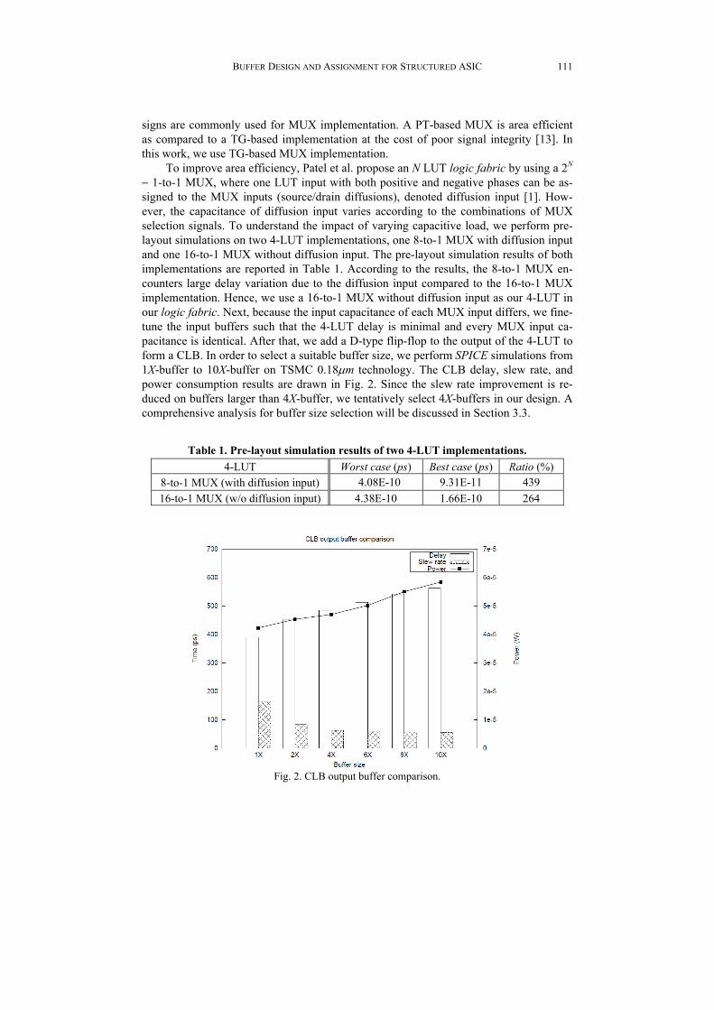
To improve area efficiency, Patel et al. propose an N LUT logic fabric by using a 2N 1-to-1 MUX, where one LUT input with both positive and negative phases can be as-signed to the MUX inputs (source/drain diffusions), denoted diffusion input [1]. How-ever, the capacitance of diffusion input varies according to the combinations of MUX selection signals. To understand the impact of varying capacitive load, we perform pre- layout simulations on two 4-LUT implementations, one 8-to-1 MUX with diffusion input and one 16-to-1 MUX without diffusion input. The pre-layout simulation results of both implementations are reported in Table 1. According to the results, the 8-to-1 MUX en-counters large delay variation due to the diffusion input compared to the 16-to-1 MUX implementation. Hence, we use a 16-to-1 MUX without diffusion input as our 4-LUT in our logic fabric. Next, because the input capacitance of each MUX input differs, we fine- tune the input buffers such that the 4-LUT delay is minimal and every MUX input ca-pacitance is identical. After that, we add a D-type flip-flop to the output of the 4-LUT to form a CLB. In order to select a suitable buffer size, we perform SPICE simulations from 1X-buffer to 10X-buffer on TSMC 0.18m technology. The CLB delay, slew rate, and power consumption results are drawn in Fig. 2. Since the slew rate improvement is re-duced on buffers larger than 4X-buffer, we tentatively select 4X-buffers in our design. A comprehensive analysis for buffer size selection will be discussed in Section 3.3.
Table 1. Pre-layout simulation results of two 4-LUT implementations.
4-LUT Worst case (ps) Best case (ps) Ratio (%)
8-to-1 MUX (with diffusion input) 4.08E-10 9.31E-11 439
16-to-1 MUX (w/o diffusion input) 4.38E-10 1.66E-10 264
Fig. 2. CLB output buffer comparison.
PO-YANG HSU AND YI-YU LIU
112
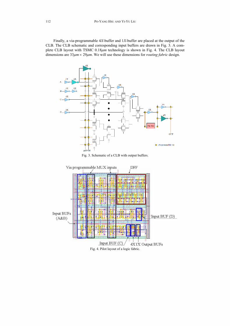
Finally, a via-programmable 4X-buffer and 1X-buffer are placed at the output of the CLB. The CLB schematic and corresponding input buffers are drawn in Fig. 3. A com-plete CLB layout with TSMC 0.18m technology is shown in Fig. 4. The CLB layout dimensions are 33m 29m. We will use these dimensions for routing fabric design.
Fig. 3. Schematic of a CLB with output buffers.
Fig. 4. Pilot layout of a logic fabric.
BUFFER DESIGN AND ASSIGNMENT FOR STRUCTURED ASIC
113
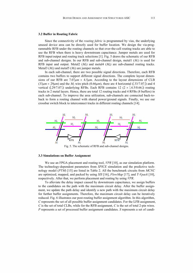
3.2 Buffer in Routing Fabric Since the connectivity of the routing fabric is programmed by vias, the underlying
unused device area can be directly used for buffer location. We design the via-prog- rammable RFB under the routing channels so that over-the-cell routing tracks are able to use the RFB when there is heavy downstream capacitance. Jumper metals are used for RFB input/output and routing track selections [1]. Fig. 5 draws the schematic of our RFB and sub-channel designs. In our RFB and sub-channel design, metal1 (M1) is used for RFB input and output. Metal2 (M2) and metal4 (M4) are sub-channel routing tracks. Metal3 (M3) and metal5 (M5) are jumper metals.
In each sub-channel, there are two possible signal directions. Therefore, each RFB contains two buffers to support different signal directions. The complete layout dimen-sions of our RFB are 7.07m 4.5m. According to the layout dimensions of CLB (33m 29m) and the M2 wire pitch (0.66m), there are 4 horizontal (33/7.07) and 4 vertical (29/7.07) underlying RFBs. Each RFB contains 12 (2 4.5/0.66) routing tracks in 2 metal layers. Hence, there are total 12 routing tracks and 4 RFBs (8 buffers) in each sub-channel. To improve the area utilization, sub-channels are connected back-to- back to form a routing channel with shared power/ground signals. Finally, we use our crossbar switch block to interconnect tracks in different routing channels [14].
Fig. 5. The schematic of RFB and sub-channel designs.
3.3 Simulations on Buffer Assignment We use an FPGA placement and routing tool, VPR [10], as our simulation platform.
The technology-dependent parameters from SPICE simulation and the predictive tech-nology model (PTM) [15] are listed in Table 2. All the benchmark circuits from MCNC are optimized, mapped, and packed by using SIS [16], FlowMap [17], and T-Vpack [10], respectively. After that, we perform placement and routing by using VPR.
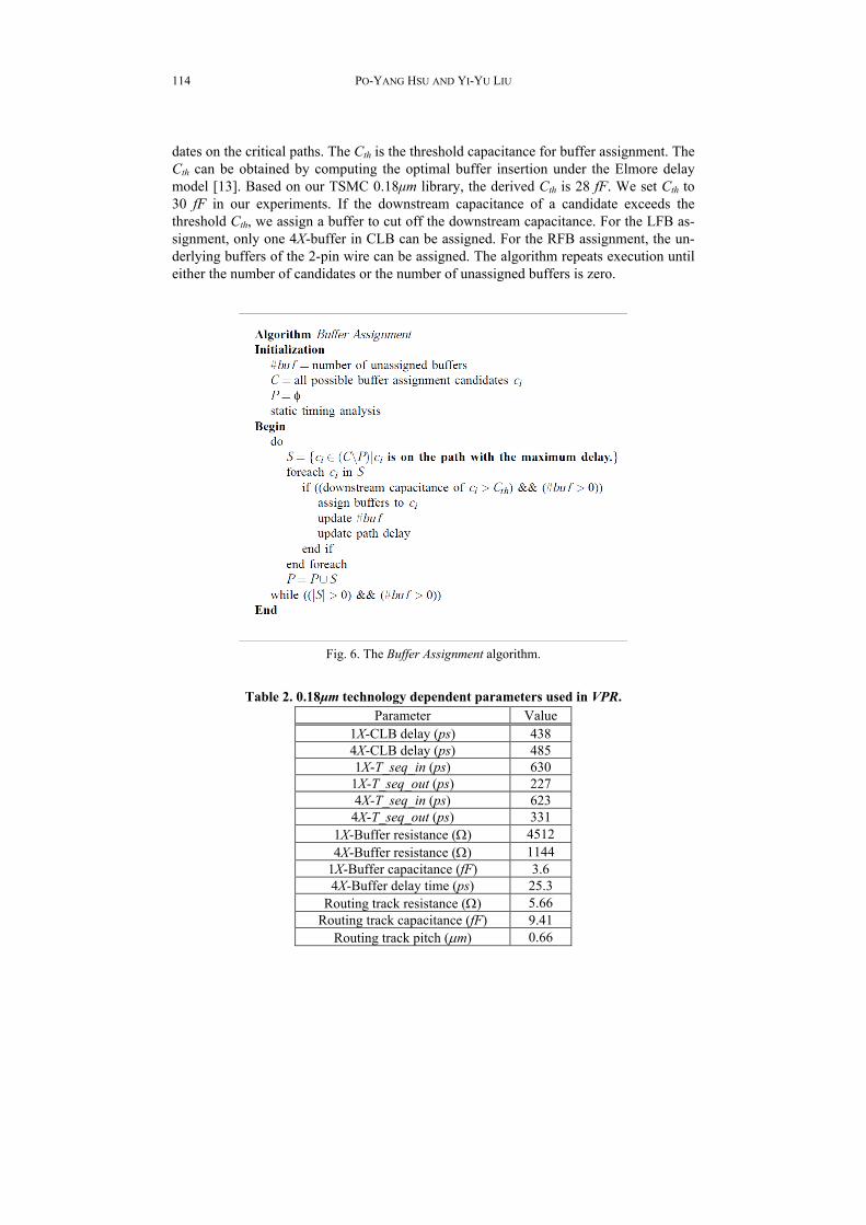
To alleviate the delay impact caused by downstream capacitance, we assign buffers to the candidates on the path with the maximum circuit delay. After the buffer assign-ment, we update the path delay and identify a new path with the maximum circuit delay for further buffer assignments. Therefore, the maximum circuit delay can be iteratively reduced. Fig. 6 illustrates our post-routing buffer assignment algorithm. In this algorithm, C represents the set of all possible buffer assignment candidates. For the LFB assignment, C is the set of total CLBs, while for the RFB assignment, C is the set of total 2-pin wires. P represents a set of processed buffer assignment candidates. S represents a set of candi-
PO-YANG HSU AND YI-YU LIU
114
dates on the critical paths. The Cth is the threshold capacitance for buffer assignment. The Cth can be obtained by computing the optimal buffer insertion under the Elmore delay model [13]. Based on our TSMC 0.18μm library, the derived Cth is 28 fF. We set Cth to 30 fF in our experiments. If the downstream capacitance of a candidate exceeds the threshold Cth, we assign a buffer to cut off the downstream capacitance. For the LFB as-signment, only one 4X-buffer in CLB can be assigned. For the RFB assignment, the un-derlying buffers of the 2-pin wire can be assigned. The algorithm repeats execution until either the number of candidates or the number of unassigned buffers is zero.
Fig. 6. The Buffer Assignment algorithm.
Table 2. 0.18μm technology dependent parameters used in VPR. Parameter Value
1X-CLB delay (ps) 438 4X-CLB delay (ps) 485 1X-T_seq_in (ps) 630
1X-T_seq_out (ps) 227 4X-T_seq_in (ps) 623
4X-T_seq_out (ps) 331 1X-Buffer resistance () 4512 4X-Buffer resistance () 1144
1X-Buffer capacitance (fF) 3.6 4X-Buffer delay time (ps) 25.3
Routing track resistance () 5.66 Routing track capacitance (fF) 9.41
Routing track pitch (m) 0.66
BUFFER DESIGN AND ASSIGNMENT FOR STRUCTURED ASIC
115
We conduct a series of pilot experiments to evaluate various LFB and RFB con-figurations. The average simulation results are summarized in Table 3. Rows LFB repre-sent the results of various LFB sizes. Row LFB + unused CLB represents the result tak-ing all unused CLBs as buffers. Row LFB + RFB represents the result with the combined LFB and RFB assignment. All the delay results are normalized to the result of 1X-LFB in column Dratio. We record the ratio of wire delay to gate delay of the new critical path af-ter buffer assignment in column Dw/Dg to demonstrate the effectiveness of pre-fabricated buffers. From Table III, both circuit performance and the ratio of wire delay to gate delay are greatly improved when we use large LFB. However, with the size of LFB increases, the aforementioned improvement rates are drastically reduced especially when the LFB size is larger than 4X. Therefore, we cannot tackle capacitive load problem by using LFB only. Similarly, according to the result of using unused CLBs as buffers, we can slightly improve circuit performance and the ratio of wire delay to gate delay. However, the maximum channel width may be increased since extra routing wires are required to make use of the unused CLBs. In order to keep the placement and routing results unaltered, we suggest not to use the unused CLBs for buffer assignment. Finally, the combined LFB and RFB assignment achieves the best results in terms of circuit performance and the ratio of wire delay to gate delay. Based on the above simulation results, we select 4X LFB and RFB in our design.
Table 3. Simulation results of different buffer assignments. Buffer assignment Buffer size Dratio (%) Dw/Dg
LFB 1X 100.0 32.6 LFB 2X 53.5 16.9 LFB 4X 29.8 8.2 LFB 6X 22.1 5.7 LFB 8X 18.2 3.9
LFB + unused LFB 4X 27.8 7.6
LFB + RFB 4X 10.4 0.8
4. CHANNEL MIGRATION
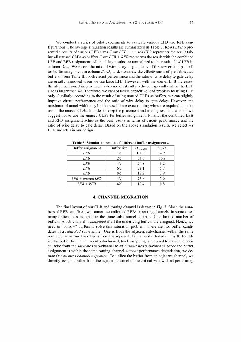
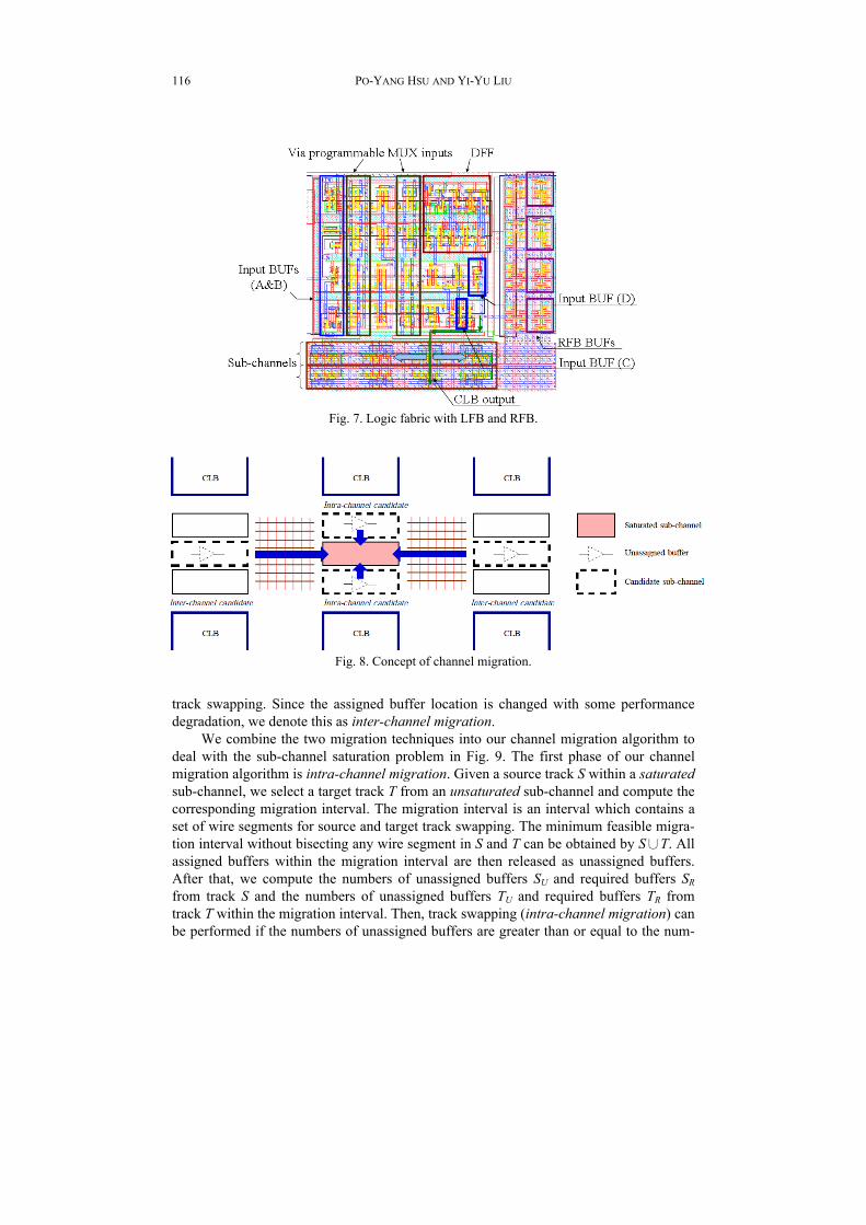
The final layout of our CLB and routing channel is drawn in Fig. 7. Since the num-bers of RFBs are fixed, we cannot use unlimited RFBs in routing channels. In some cases, many critical nets assigned to the same sub-channel compete for a limited number of buffers. A sub-channel is saturated if all the underlying buffers are assigned. Hence, we need to “borrow” buffers to solve this saturation problem. There are two buffer candi-dates of a saturated sub-channel. One is from the adjacent sub-channel within the same routing channel and the other is from the adjacent channel as illustrated in Fig. 8. To util-ize the buffer from an adjacent sub-channel, track swapping is required to move the criti-cal wire from the saturated sub-channel to an unsaturated sub-channel. Since the buffer assignment is within the same routing channel without performance degradation, we de-note this as intra-channel migration. To utilize the buffer from an adjacent channel, we directly assign a buffer from the adjacent channel to the critical wire without performing
PO-YANG HSU AND YI-YU LIU
116
Fig. 7. Logic fabric with LFB and RFB.
Fig. 8. Concept of channel migration.
track swapping. Since the assigned buffer location is changed with some performance degradation, we denote this as inter-channel migration.
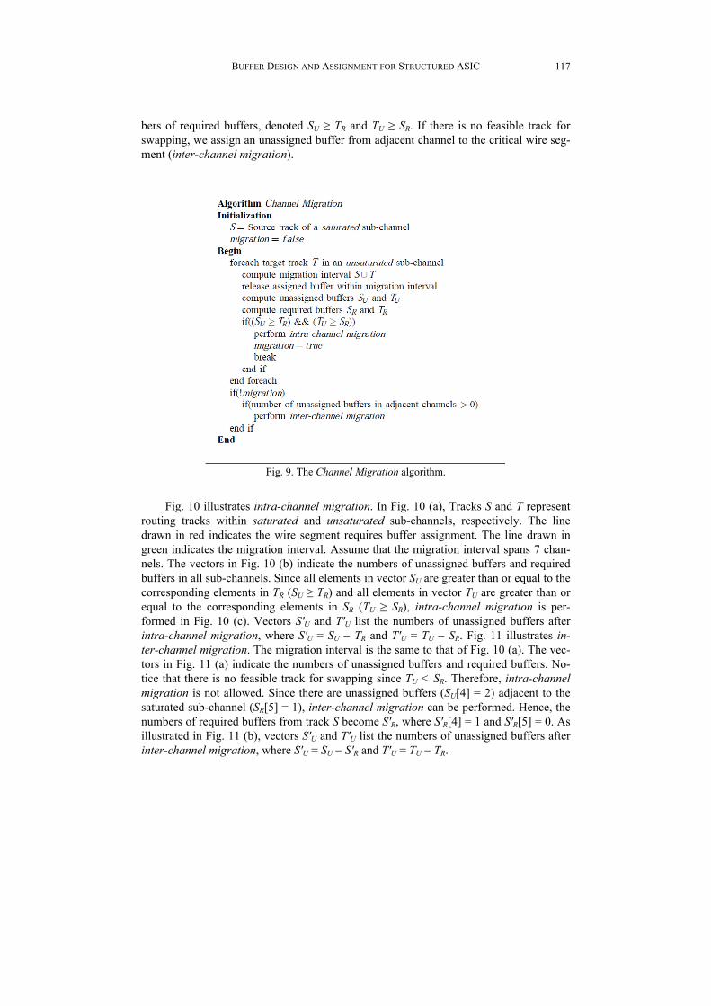
We combine the two migration techniques into our channel migration algorithm to deal with the sub-channel saturation problem in Fig. 9. The first phase of our channel migration algorithm is intra-channel migration. Given a source track S within a saturated sub-channel, we select a target track T from an unsaturated sub-channel and compute the corresponding migration interval. The migration interval is an interval which contains a set of wire segments for source and target track swapping. The minimum feasible migra-tion interval without bisecting any wire segment in S and T can be obtained by S∪T. All assigned buffers within the migration interval are then released as unassigned buffers. After that, we compute the numbers of unassigned buffers SU and required buffers SR from track S and the numbers of unassigned buffers TU and required buffers TR from track T within the migration interval. Then, track swapping (intra-channel migration) can be performed if the numbers of unassigned buffers are greater than or equal to the num-
BUFFER DESIGN AND ASSIGNMENT FOR STRUCTURED ASIC
117
bers of required buffers, denoted SU ≥ TR and TU ≥ SR. If there is no feasible track for swapping, we assign an unassigned buffer from adjacent channel to the critical wire seg-ment (inter-channel migration).
Fig. 9. The Channel Migration algorithm.
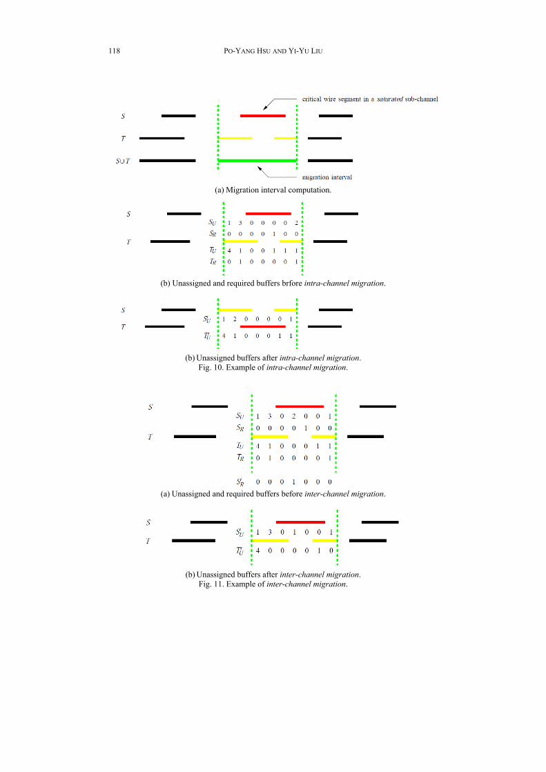
Fig. 10 illustrates intra-channel migration. In Fig. 10 (a), Tracks S and T represent routing tracks within saturated and unsaturated sub-channels, respectively. The line drawn in red indicates the wire segment requires buffer assignment. The line drawn in green indicates the migration interval. Assume that the migration interval spans 7 chan-nels. The vectors in Fig. 10 (b) indicate the numbers of unassigned buffers and required buffers in all sub-channels. Since all elements in vector SU are greater than or equal to the corresponding elements in TR (SU ≥ TR) and all elements in vector TU are greater than or equal to the corresponding elements in SR (TU ≥ SR), intra-channel migration is per-formed in Fig. 10 (c). Vectors S'U and T'U list the numbers of unassigned buffers after intra-channel migration, where S'U = SU TR and T'U = TU SR. Fig. 11 illustrates in-ter-channel migration. The migration interval is the same to that of Fig. 10 (a). The vec-tors in Fig. 11 (a) indicate the numbers of unassigned buffers and required buffers. No-tice that there is no feasible track for swapping since TU < SR. Therefore, intra-channel migration is not allowed. Since there are unassigned buffers (SU[4] = 2) adjacent to the saturated sub-channel (SR[5] = 1), inter-channel migration can be performed. Hence, the numbers of required buffers from track S become S'R, where S'R[4] = 1 and S'R[5] = 0. As illustrated in Fig. 11 (b), vectors S'U and T'U list the numbers of unassigned buffers after inter-channel migration, where S'U = SU S'R and T'U = TU TR.
PO-YANG HSU AND YI-YU LIU
118
(a) Migration interval computation.
(b) Unassigned and required buffers brfore intra-channel migration.
(b) Unassigned buffers after intra-channel migration.
Fig. 10. Example of intra-channel migration.
(a) Unassigned and required buffers before inter-channel migration.
(b) Unassigned buffers after inter-channel migration.
Fig. 11. Example of inter-channel migration.
BUFFER DESIGN AND ASSIGNMENT FOR STRUCTURED ASIC
119
5. EXPERIMENTAL RESULTS
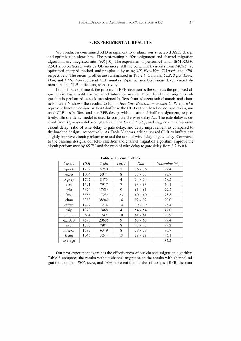
We conduct a constrained RFB assignment to evaluate our structured ASIC design and optimization algorithms. The post-routing buffer assignment and channel migration algorithms are integrated into VPR [10]. The experiment is performed on an IBM X3550 2.5GHz Xeon Server with 32 GB memory. All the benchmark circuits from MCNC are optimized, mapped, packed, and pre-placed by using SIS, FlowMap, T-Vpack, and VPR, respectively. The circuit profiles are summarized in Table 4. Columns CLB, 2-pin, Level, Dim, and Utilization represent CLB number, 2-pin net number, circuit level, circuit di-mension, and CLB utilization, respectively.
In our first experiment, the priority of RFB insertion is the same as the proposed al-gorithm in Fig. 6 until a sub-channel saturation occurs. Then, the channel migration al-gorithm is performed to seek unassigned buffers from adjacent sub-channels and chan-nels. Table V shows the results. Columns Baseline, Baseline + unused CLB, and RFB represent baseline designs with 4X-buffer at the CLB output, baseline designs taking un-used CLBs as buffers, and our RFB design with constrained buffer assignment, respec-tively. Elmore delay model is used to compute the wire delay Dw. The gate delay is de-rived from Dg = gate delay × gate level. The Delay, Dw/Dg, and Dimp columns represent circuit delay, ratio of wire delay to gate delay, and delay improvement as compared to the baseline designs, respectively. As Table V shows, taking unused CLB as buffers can slightly improve circuit performance and the ratio of wire delay to gate delay. Compared to the baseline designs, our RFB insertion and channel migration algorithm improve the circuit performance by 65.7% and the ratio of wire delay to gate delay from 8.2 to 0.8.
Table 4. Circuit profiles.
Circuit CLB 2-pin Level Dim Utilization (%)
apex4 1262 5750 7 36 36 97.4 ex5p 1064 5074 8 33 33 97.7
bigkey 1707 8473 4 54 54 58.5 des 1591 7957 7 63 63 40.1 spla 3690 17514 9 61 61 99.2 frisc 3556 17234 23 60 60 98.8 clma 8383 38940 16 92 92 99.0 diffeq 1497 7234 14 39 39 98.4 dsip 1370 7468 4 54 54 47.0
elliptic 3604 17491 18 61 61 96.9 ex1010 4598 20686 9 68 68 99.4
seq 1750 7984 8 42 42 99.2 misex3 1397 6379 8 38 38 96.7 tseng 1047 5244 13 33 33 96.1
average 87.5
Our next experiment examines the effectiveness of our channel migration algorithm. Table 6 compares the results without channel migration to the results with channel mi-gration. Columns RFB, Intra, and Inter represent the number of assigned RFB, the num-
PO-YANG HSU AND YI-YU LIU
120
Table 5. The results of constrained RFB insertion.
Baseline Baseline + unused CLB RFB Circuit
Delay Dw/Dg Delay Dimp (%) Dw/Dg Delay Dimp (%) Dw/Dg
apex4 1.64E-08 3.4 1.38E-08 15.7 2.8 7.20E-09 56.1 1.0 ex5p 1.74E-08 3.2 1.74E-08 0.0 3.2 6.65E-09 61.7 0.6
bigkey 2.79E-08 12.5 2.74E-08 1.7 12.2 4.61E-09 83.5 1.2 des 2.51E-08 6.8 1.36E-08 45.7 3.3 5.97E-09 76.2 0.9 spla 2.91E-08 5.3 2.91E-08 0.0 5.3 1.12E-08 61.6 1.4 frisc 4.86E-08 15.0 4.76E-08 2.0 14.7 1.56E-08 68.0 0.3 clma 5.68E-08 6.2 5.59E-08 1.6 6.1 1.37E-08 75.9 0.8 diffeq 1.76E-08 5.9 1.58E-08 10.0 5.2 8.84E-09 49.8 0.2 dsip 3.31E-08 15.0 3.26E-08 1.6 14.7 4.53E-09 86.3 1.2
elliptic 4.84E-08 22.4 4.60E-08 4.9 21.2 1.13E-08 76.6 0.5 ex1010 3.81E-08 7.2 3.81E-08 0.0 7.2 1.06E-08 72.2 1.3
seq 1.59E-08 2.8 1.53E-08 3.8 2.7 6.98E-09 56.0 0.7 misex3 1.45E-08 2.9 1.45E-08 0.0 2.9 7.40E-09 49.1 1.0 tseng 1.61E-08 6.8 1.36E-08 15.3 5.6 8.54E-09 47.0 0.3
average 8.2 7.3 7.6 65.7 0.8
Table 6. The results of constrained RFB insertion with and without channel migrations. Without channel migration With channel migration
Circuit Delay Dw/Dg RFB Delay Dimp (%) Dw/Dg RFB Intra Inter
apex4 7.20E-09 1.0 6655 7.20E-09 0.0 1.0 6670 16 15 ex5p 9.27E-09 1.2 1629 6.65E-09 28.3 0.6 2528 1 2
bigkey 4.61E-09 1.2 2289 4.61E-09 0.0 1.2 2289 0 0 des 5.97E-09 0.9 1582 5.97E-09 0.0 0.9 1582 0 0 spla 1.76E-08 2.8 5902 1.12E-08 36.5 1.4 10416 3 5 frisc 1.56E-08 0.3 3376 1.56E-08 0.0 0.3 3376 0 0 clma 1.37E-08 0.8 43324 1.37E-08 0.0 0.8 43436 94 116 diffeq 8.84E-09 0.2 1443 8.84E-09 0.0 0.2 1443 0 0 dsip 4.53E-09 1.2 1870 4.53E-09 0.0 1.2 1870 0 0
elliptic 1.51E-08 1.0 3575 1.13E-08 25.3 0.5 6111 1 1 ex1010 1.15E-08 2.1 7844 1.06E-08 8.0 1.3 10785 3 1
seq 1.31E-08 2.6 1259 6.98E-09 46.9 0.7 3865 2 3 misex3 1.15E-08 2.1 1969 7.40E-09 35.7 1.0 2766 1 1 tseng 8.54E-09 0.3 817 8.54E-09 0.0 0.3 817 0 0
average 1.3 82.5% 12.9 0.8 100%
ber of intra-channel migrations, and the number of inter-channel migrations, respectively. From Table 6, our channel migration algorithm improves circuit performance by 12.9%. Additionally, the ratio of the wire delay to gate delay is reduced from 1.3 to 0.8.
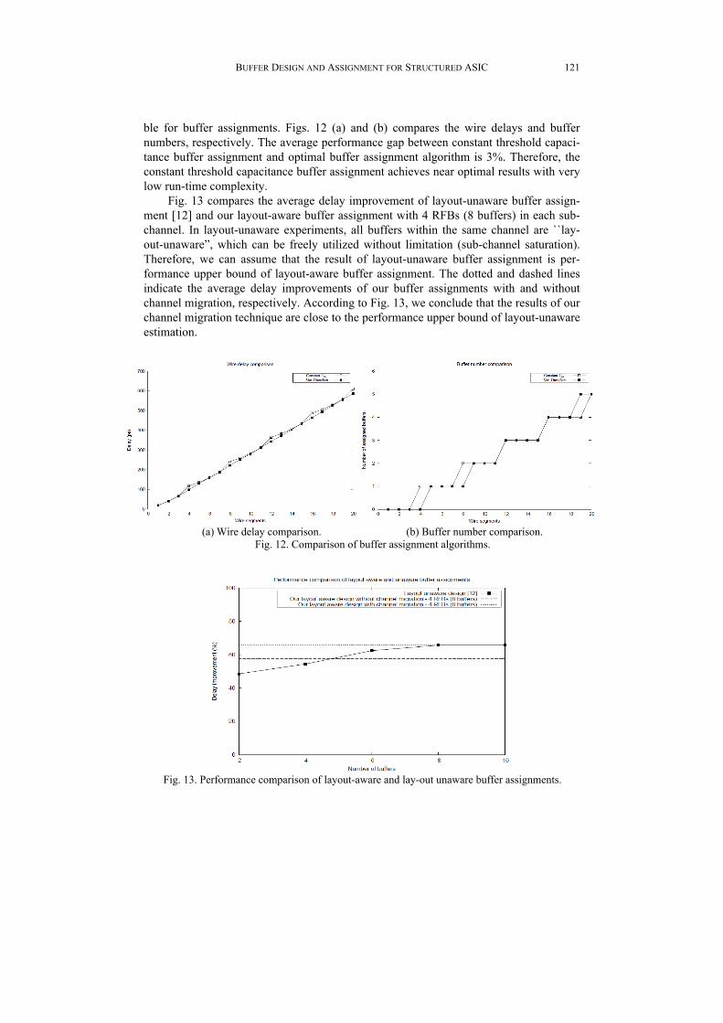
To understand the performance gap between our constant threshold capacitance (Cth) buffer assignment and delay-optimal buffer assignment algorithm [8, 9]. We perform simulations on wires with lengths from 1 channel to 20 channels. All channels are eligi-
BUFFER DESIGN AND ASSIGNMENT FOR STRUCTURED ASIC
121
Fig. 13. Performance comparison of layout-aware and lay-out unaware buffer assignments.
ble for buffer assignments. Figs. 12 (a) and (b) compares the wire delays and buffer numbers, respectively. The average performance gap between constant threshold capaci-tance buffer assignment and optimal buffer assignment algorithm is 3%. Therefore, the constant threshold capacitance buffer assignment achieves near optimal results with very low run-time complexity.
Fig. 13 compares the average delay improvement of layout-unaware buffer assign-ment [12] and our layout-aware buffer assignment with 4 RFBs (8 buffers) in each sub- channel. In layout-unaware experiments, all buffers within the same channel are ``lay-out-unaware”, which can be freely utilized without limitation (sub-channel saturation). Therefore, we can assume that the result of layout-unaware buffer assignment is per-formance upper bound of layout-aware buffer assignment. The dotted and dashed lines indicate the average delay improvements of our buffer assignments with and without channel migration, respectively. According to Fig. 13, we conclude that the results of our channel migration technique are close to the performance upper bound of layout-unaware estimation.
(a) Wire delay comparison. (b) Buffer number comparison.
Fig. 12. Comparison of buffer assignment algorithms.
PO-YANG HSU AND YI-YU LIU
122
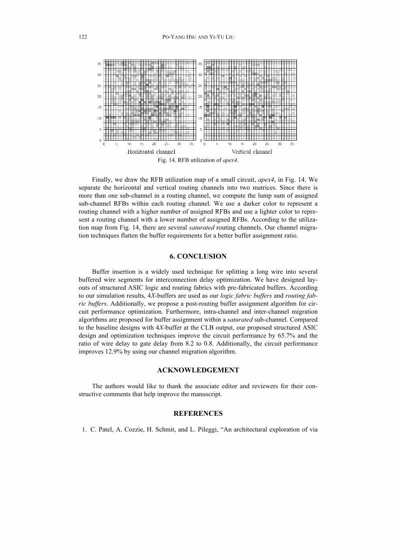
Fig. 14. RFB utilization of apex4.
Finally, we draw the RFB utilization map of a small circuit, apex4, in Fig. 14. We separate the horizontal and vertical routing channels into two matrices. Since there is more than one sub-channel in a routing channel, we compute the lump sum of assigned sub-channel RFBs within each routing channel. We use a darker color to represent a routing channel with a higher number of assigned RFBs and use a lighter color to repre-sent a routing channel with a lower number of assigned RFBs. According to the utiliza-tion map from Fig. 14, there are several saturated routing channels. Our channel migra-tion techniques flatten the buffer requirements for a better buffer assignment ratio.
6. CONCLUSION
Buffer insertion is a widely used technique for splitting a long wire into several buffered wire segments for interconnection delay optimization. We have designed lay-outs of structured ASIC logic and routing fabrics with pre-fabricated buffers. According to our simulation results, 4X-buffers are used as our logic fabric buffers and routing fab-ric buffers. Additionally, we propose a post-routing buffer assignment algorithm for cir-cuit performance optimization. Furthermore, intra-channel and inter-channel migration algorithms are proposed for buffer assignment within a saturated sub-channel. Compared to the baseline designs with 4X-buffer at the CLB output, our proposed structured ASIC design and optimization techniques improve the circuit performance by 65.7% and the ratio of wire delay to gate delay from 8.2 to 0.8. Additionally, the circuit performance improves 12.9% by using our channel migration algorithm.
ACKNOWLEDGEMENT
The authors would like to thank the associate editor and reviewers for their con-structive comments that help improve the manuscript.
REFERENCES
1. C. Patel, A. Cozzie, H. Schmit, and L. Pileggi, “An architectural exploration of via
BUFFER DESIGN AND ASSIGNMENT FOR STRUCTURED ASIC
123
patterned gate arrays,” in Proceedings of International Symposium on Physical De-sign, 2003, pp. 184-189.
2. B. Hu, H. Jiang, Q. Liu, and M. M. Sadowska, ”Synthesis and placement flow for gain-based programmable regular fabrics,” in Proceedings of International Sympo-sium on Physical Design, 2003, pp. 197-203.
3. N. Jayakumar and S. P. Khatri, “A metal and via maskset programmable VLSI de-sign methodology using PLAs,” in Proceedings of International Conference on Computer-Aided Design, 2004, pp. 590-594.
4. Y. Ran and M. Marek-Sadowska, “Via-configurable routing architectures and fast design mappability estimation for regular fabrics,” in Proceedings of International Conference on Computer-Aided Design, 2005, pp. 25-32.
5. K. Gulati, N. Jayakumar, and S. P. Khatri, “A structured ASIC design approach us-ing pass transistor logic,” in Proceedings of IEEE International Symposium on Cir-cuits and Systems, 2007, pp. 1787-1790.
6. S. Gopalani, R. Garg, S. P. Khatri, and M. Cheng, “A lithography-friendly structured ASIC design approach,” in Proceedings of Great Lakes Symposium on VLSI, 2008, pp. 315-320.
7. U. Ahmed, G. G. F. Lemieux, and S. J. E. Wilton, “Area, delay, power, and cost trends for metal-programmable structured ASICs (MPSAs),” in Proceedings of In-ternational Conference on Field Programmable Technology, 2009, pp. 278-284.
8. L. P. P. P. van Ginncken, “Buffer placement in distributed RC-tree networks for mi- nimal elmore delay,” in Proceedings of International Symposium on Circuits and Systems, 1990, pp. 865-868.
9. Y. Gao and D. F. Wong, “A graph based algorithm for optimal buffer insertion under accurate delay models,” in Proceedings of Design Automation and Test in Europe, 2001, pp. 535-539.
10. V. Betz, J. Rose, and A. Marquardt, Architecture and CAD for Deep-Submicron FPGAs, Kluwer Academic Publishers, MA, 1999.
11. D. Chen, J. Cong, and P. Pan, FPGA Design Automation, Now Publishers, __(place), 2006.
12. T. Zhang and S. S. Sapatnekar, “Buffering global interconnects in structured ASIC design,” in Proceedings of Conference on Asia and South Pacific Design Automation, 2005, pp. 23-26.
13. N. H. E. Weste and D. Harris, CMOS VLSI Design: a Circuit and Systems Perspec-tive, Addison Wesley, MA, 2004.
14. Y. H. Hung, H. Y. Li, P. Y. Hsu, and Y. Y. Liu, “Dangling-wire avoidance routing for crossbar switch structured ASIC design style,” in Proceedings of IEEE Interna-tional Symposium on VLSI Design, Automation, and Test, 2010, pp. 177-180.
15. The predictive technology model (PTM) 2007, http://www.eas.asu.edu/~ptm/. 16. E. M. Sentovich, K. J. Singh, L. Lavagno, C. Moon, R. Murgai, A. Saldanha, H.
Savoj, P. R. Stephan, R. K. Brayton, and A. Sangiovanni-Vincentelli, “SIS: A sys-tem for sequential circuit synthesis,” Electronics Research Laboratory, Memoran-dum No. UCB/ERL M92/41, 1992.
17. J. Cong and Y. Ding, “Flowmap: an optimal technology mapping algorithm for delay optimization in lookup-table based FPGA designs,” IEEE Transactions on Compu- ter-Aided Design of Integrated Circuits and Systems, Vol. 13, 1994, pp. 1-12.
PO-YANG HSU AND YI-YU LIU
124
Po-Yang Hsu (許博揚) received the B.S. degree in Com-puter Science from Yuan Ze University in 2008. He received the M.S. degrees from the same university in 2010. Currently, he is pursuing the Ph.D. degree in National Tsing Hua University. His research interests include physical design automation, and com-puter architecture.
Yi-Yu Liu (劉一宇) received the B.S. degree in Physics from National Tsing Hua University in 1997. He received the M.S. and the Ph.D. degrees from the same university in 2000 and 2006, respectively, all in Computer Science. Currently, he is an Assistant Professor in the Department of Computer Science and Engineering, Yuan Ze University. His research interests include technology dependent logic synthesis, physical design automation, and computer architecture.