BU97981xxx Series : LED / LCD Drivers -...
49
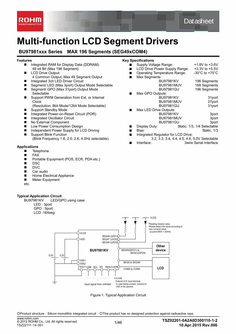
○Product structure:Silicon monolithic integrated circuit ○This product has no designed protection against radioactive rays. 1/46 TSZ02201-0A2A0D300110-1-2 10.Apr.2015 Rev.006 www.rohm.com © 2012 ROHM Co., Ltd. All rights reserved. TSZ22111・14・001 Multi-function LCD Segment Drivers BU97981xxx Series MAX 196 Segments (SEG49xCOM4) Features Integrated RAM for Display Data (DDRAM): 49 x4 Bit (Max 196 Segment) LCD Drive Output: 4 Common Output, Max 49 Segment Output Integrated 3ch LED Driver Circuit Segment/ LED (Max 3port) Output Mode Selectable Segment/ GPO (Max 31port) Output Mode Selectable Support PWM Generation from Ext. or Internal Clock (Resolution: 8bit Mode/12bit Mode Selectable) Support Standby Mode Integrated Power-on-Reset Circuit (POR) Integrated Oscillator Circuit No External Component Low Power Consumption Design Independent Power Supply for LCD Driving Support Blink Function (Blink Frequency 1.6, 2.0, 2.6, 4.0Hz selectable) Applications Telephone FAX Portable Equipment (POS, ECR, PDA etc.) DSC DVC Car audio Home Electrical Appliance Meter Equipment etc. Key Specifications ■ Supply Voltage Range: +1.8V to +3.6V ■ LCD Drive Power Supply Range: +3.3V to +5.5V ■ Operating Temperature Range: -30°C to +75°C ■ Max Segments: BU97981KV 196 Segments BU97981MUV 168 Segments BU97981GU 196 Segments ■ Max GPO Outputs: BU97981KV 31port BU97981MUV 27port BU97981GU 31port ■ Max LED Drive Outputs: BU97981KV 3port BU97981MUV 3port BU97981GU 3port ■ Display Duty: Static. 1/3, 1/4 Selectable ■ Bias: Static, 1/3 ■ Integrated Regulator for LCD Drive: 3.2, 3.3, 3.4, 4.4, 4.5, 4.6, 5.0V Selectable ■ Interface: 3wire Serial Interface Typical Application Circuit BU97981KV LED/GPO using case LED : 3port GPO : 5port LCD :164seg *Reading resistor value Please detect the value according to inpu curremt value. (cuurent MAX = 20mA) 5.0V 3.3V VLCD VDD CLKIN CSB SCL SD VSS1 BU97981KV LCD COM0 to COM3 SEG0 to SEG40 SEG48 (LED1) Input signal from cintroller *CLKIN Extenal CLK input terminal In case being unused, connect to VSS or be opened. INHb VSS2 TEST1 VLED SEG45(GPO1) to SEG41(GPO5) Other device SEG47 (LED2) SEG46 (LED3) Figure 1. Typical Application Circuit Datasheet
-
Upload
nguyenkhanh -
Category
Documents
-
view
215 -
download
0
Transcript of BU97981xxx Series : LED / LCD Drivers -...
○Product structure:Silicon monolithic integrated circuit ○This product has no designed protection against radioactive rays.
1/46 TSZ02201-0A2A0D300110-1-2
10.Apr.2015 Rev.006
www.rohm.com © 2012 ROHM Co., Ltd. All rights reserved. TSZ22111・14・001
Multi-function LCD Segment Drivers BU97981xxx Series MAX 196 Segments (SEG49xCOM4)
Features
Integrated RAM for Display Data (DDRAM): 49 x4 Bit (Max 196 Segment) LCD Drive Output: 4 Common Output, Max 49 Segment Output Integrated 3ch LED Driver Circuit Segment/ LED (Max 3port) Output Mode Selectable Segment/ GPO (Max 31port) Output Mode
Selectable Support PWM Generation from Ext. or Internal
Clock (Resolution: 8bit Mode/12bit Mode Selectable)
Support Standby Mode Integrated Power-on-Reset Circuit (POR) Integrated Oscillator Circuit No External Component Low Power Consumption Design Independent Power Supply for LCD Driving Support Blink Function
(Blink Frequency 1.6, 2.0, 2.6, 4.0Hz selectable)
Applications
Telephone FAX Portable Equipment (POS, ECR, PDA etc.) DSC DVC Car audio Home Electrical Appliance Meter Equipment etc.
Key Specifications
■ Supply Voltage Range: +1.8V to +3.6V ■ LCD Drive Power Supply Range: +3.3V to +5.5V ■ Operating Temperature Range: -30°C to +75°C ■ Max Segments:
BU97981KV 196 Segments BU97981MUV 168 Segments BU97981GU 196 Segments
■ Max GPO Outputs: BU97981KV 31port BU97981MUV 27port BU97981GU 31port
■ Max LED Drive Outputs: BU97981KV 3port BU97981MUV 3port BU97981GU 3port
■ Display Duty: Static. 1/3, 1/4 Selectable ■ Bias: Static, 1/3 ■ Integrated Regulator for LCD Drive:
3.2, 3.3, 3.4, 4.4, 4.5, 4.6, 5.0V Selectable ■ Interface: 3wire Serial Interface
Typical Application Circuit
BU97981KV LED/GPO using case LED : 3port GPO : 5port LCD :164seg
*Reading resistor value Please detect the value according toinpu curremt value.(cuurent MAX = 20mA)
5.0V 3.3V
VLCD
VDD
CLKINCSB SCL SD
VSS1
BU97981KV
LCDCOM0 to COM3
SEG0 to SEG40
SEG48 (LED1)
Input signal from cintroller
*CLKIN
Extenal CLK input terminal
In case being unused, connect toVSS or be opened.
INHb
VSS2
TEST1
VLED
SEG45(GPO1) toSEG41(GPO5)
Otherdevice
SEG47 (LED2)
SEG46 (LED3)
Figure 1. Typical Application Circuit
Datasheet

2/46
BU97981xxx Series MAX 196 segments (SEG49xCOM4) Datasheet
TSZ02201-0A2A0D300110-1-2
10.Apr.2015 Rev.006
www.rohm.com © 2012 ROHM Co., Ltd. All rights reserved. TSZ22111・15・001
blink timing generator
common counter
INHb
CLKIN
PWM
Generator
OSCILLATOR
Ref Voltage Circuit
Output
Controller
LCD BIAS
SELECTOR
common
driver
Power On Reset
SD SCL
VSS
VSS
COM0……COM3 SEG0 ……………………………… SEG48
IF FILTER
serial inter face
DDRAM GPO data latch
LCD voltage Generator
Command register Data Decoder
VLCD
CSB
VDD
Segment
driver
Segment
driver/LED
GPO/LED Controller
Segment
driver/GPO
PWMOUT
VSS2
TEST1
Vreg
Block Diagram / Pin Arrangement / Pin Description
BU97981KV
Figure 2. Block Diagram Figure 3. Pin Configuration (TOP VIEW)
Table 1. Pin Description
Terminal Terminal number
I/O Unused case Function
CSB 1 I - Chip select: "L" active
SCL 2 I - Serial data transfer clock
SD 3 I - Input serial data
VDD 4 - - Power supply for LOGIC
CLKIN 64 I OPEN / VSS External clock input terminal (for display/PWM using selectable) Support Hi-Z input mode at internal clock mode
TEST1 5 I - TEST terminal (Please connect VSS terminal)
VSS1 6 - - GND
VLCD 8 - - Power supply for LCD
INHb 7 I VDD
Display turning on/off select terminal H: turning on display, L: turning off display INHb = “L”: All SEG/COM terminal : output VSS level
GPO terminal : output VSS level LED drive terminal : output Hi-Z
PWMOUT 63 O OPEN PWM output for LED2 group
COM0 to 3 9 to 12 O OPEN COMMON output for LCD
SEG0 to 14 13 to 27 O OPEN SEGMENT output for LCD
SEG15 to 45 28 to 58 O OPEN SEGMENT output for LCD/GPO
SEG46 to 48 59 to 61 O OPEN SEGMENT output for LCD/LED driver
VSS2 62 - GND GND (for SEG46-48 / LED driver)
SE
G35
SE
G34
SE
G33
SE
G32
SE
G31
SE
G30
SE
G29
SE
G28
SE
G27
SE
G26
SE
G25
SE
G24
SE
G23
SE
G22
SE
G21
SE
G20
SEG36 SEG19
SEG37 SEG18
SEG38 SEG17
SEG39 SEG16
SEG40 SEG15
SEG41 SEG14
SEG42 SEG13
SEG43 SEG12
SEG44 SEG11
SEG45 SEG10
SEG46 SEG9
SEG47 SEG8
SEG48 SEG7
VSS2 SEG6
PWMOUT SEG5
CLKIN SEG4
49
64 17
32
1 16
33
48
CS
B
SC
L
SD
VD
D
TE
ST
1
VS
S1
INH
b
VLC
D
CO
M0
CO
M1
CO
M2
CO
M3
SE
G0
SE
G1
SE
G2
SE
G3
1 16

3/46
BU97981xxx Series MAX 196 segments (SEG49xCOM4) Datasheet
TSZ02201-0A2A0D300110-1-2
10.Apr.2015 Rev.006
www.rohm.com © 2012 ROHM Co., Ltd. All rights reserved. TSZ22111・15・001
CS
B
SC
L
SD
VD
D
TE
ST
1
1 2 3 4 5 6 7 8 9 10
42 41 40 39 38 37 36 35 34 33
56
55
54
53
52
51
50
49
48
47
15
16
17
18
19
20
21
22
23
24
EXT-PAD
46
45
44
43
32 31 29
25
26
27
28
11 12 13 14
30
VS
S1
INH
b
VLC
D
CO
M0
CO
M1
CO
M2
CO
M3
SE
G0
SE
G1
SE
G29
SE
G28
SE
G27
SE
G26
SE
G25
SE
G24
SE
G23
SE
G22
SE
G21
SE
G20
SE
G19
SE
G18
SE
G17
SE
G16
SEG2
SEG3
SEG4
SEG5
SEG6
SEG7
SEG8
SEG9
SEG10
SEG11
SEG12
SEG13
SEG14
SEG15
CLKIN
VSS2
SEG41
SEG40
SEG39
SEG38
SEG37
SEG36
SEG35
SEG34
SEG33
SEG32
SEG31
SEG30
Blink timing generator
Common counter
INHb
CLKIN
PWM
Generator
Ref Voltage Circuit
LCD
BIAS SELECTOR
Common
Driver
Power On Reset
SD SCL
VSS
VSS
COM0……COM3
SEG0 …………………………….SEG48
IF FILTER
Serial inter face
DDRAM
GPO data latch
LCD voltage Generator
Command register
Data Decode
VLCD
CSB
VDD
Segment
Driver
Segment
Driver/ LED
GPO / LED
Controller
PWMOUT
VSS2
TEST1
Vreg
OSC block
CR oscillator
(typ:40.96KHz)
Clock Divider (div.2)
Segment Driver/ GPO
Output Controller
COM0 ….COM3
Block Diagram / Pin Arrangement / Pin Description
BU97981MUV
Figure 4. Block Diagram Figure 5. Pin Configuration (BOTTOM VIEW)
Table 2. Pin Description
Terminal Terminal number
I/O Unused case Function
CSB 1 I - Chip select: "L" active
SCL 2 I - Serial data transfer clock
SD 3 I - Input serial data
VDD 4 - - Power supply for LOGIC
CLKIN 56 I OPEN / VSS External clock input terminal (for display/PWM using selectable) Support Hi-Z input mode at internal clock mode
TEST1 5 I - TEST terminal (Please connect VSS terminal)
VSS1 6 - - GND
VLCD 8 - - Power supply for LCD
INHb 7 I VDD
Display turning on/off select terminal H: turning on display, L: turning off display INHb = “L”: All SEG/COM terminal : output VSS level
GPO terminal : output VSS level LED drive terminal : output Hi-Z
COM0~3 9-12 O OPEN COMMON output for LCD
SEG0~11 13-24 O OPEN SEGMENT output for LCD
SEG12~38 25-51 O OPEN SEGMENT output for LCD/GPO
SEG39~41 52-54 O OPEN SEGMENT output for LCD/LED driver
VSS2 55 - GND GND (for SEG39-41 / LED driver)
EXT-PAD -(Note1)
- VSS substrate
(Note1) To radiate heat, please contact a board with the EXT-PAD which is located at the bottom side of VQFN56AV8080 package. Please supply VSS level or Open state as the input condition for this PAD.

4/46
BU97981xxx Series MAX 196 segments (SEG49xCOM4) Datasheet
TSZ02201-0A2A0D300110-1-2
10.Apr.2015 Rev.006
www.rohm.com © 2012 ROHM Co., Ltd. All rights reserved. TSZ22111・15・001
blink timing generator
common counter
INHb
CLKIN
PWM
Generator
OSCILLATOR
Ref Voltage Circuit
Output
Controller
LCD BIAS
SELECTOR
common
driver
Power On Reset
SD SCL
VSS
VSS
COM0……COM3 SEG0 ……………………………… SEG48
IF FILTER
serial inter face
DDRAM GPO data latch
LCD voltage Generator
Command register Data Decoder
VLCD
CSB
VDD
Segment
driver
Segment
driver/LED
GPO/LED Controller
Segment
driver/GPO
PWMOUT
VSS2
Vreg
Block Diagram / Pin Arrangement / Pin Description
BU97981GU
Figure 6. Block Diagram Figure 7. Pin Configuration (TOP VIEW)
Table 3. Pin Description
Terminal I/O Unused case Function
CSB I - Chip select: "L" active
SCL I - Serial data transfer clock
SD I - Input serial data
VDD - - Power supply for LOGIC
CLKIN I OPEN / VSS External clock input terminal (for display/PWM using selectable) Support Hi-Z input mode at internal clock mode
VSS1 - - GND
VLCD - - Power supply for LCD
INHb I VDD
Display turning on/off select terminal H: turning on display, L: turning off display INHb = “L”: All SEG/COM terminal : output VSS level
GPO terminal : output VSS level LED drive terminal : output Hi-Z
PWMOUT O OPEN PWM output for LED2 group
COM0 to 3 O OPEN COMMON output for LCD
SEG0 to 14 O OPEN SEGMENT output for LCD
SEG15 to 45 O OPEN SEGMENT output for LCD/GPO
SEG46 to 48 O OPEN SEGMENT output for LCD/LED driver
VSS2 - GND GND (for SEG46-48 / LED driver)
1 2 3 4 5 6 7 8
H SEG4 SEG5 SEG9 SEG11 SEG14 SEG16 SEG18 SEG20
G SEG2 SEG3 SEG7 SEG8 SEG12 SEG17 SEG19 SEG21
F SEG0 SEG1 SEG6 SEG10 SEG13 SEG22 SEG23 SEG25
E COM2 COM0 COM1 COM3 SEG15 SEG26 SEG24 SEG27
D VLCD VDD INHB SEG47 SEG31 SEG29 SEG28 SEG30
C VSS1 SDA SCL SEG45 SEG42 SEG38 SEG33 SEG32
B (NC) CLKIN VSS2 SEG44 SEG40 SEG39 SEG35 SEG34
A CSB PWM
OUT SEG48 SEG46 SEG43 SEG41 SEG37 SEG36

5/46
BU97981xxx Series MAX 196 segments (SEG49xCOM4) Datasheet
TSZ02201-0A2A0D300110-1-2
10.Apr.2015 Rev.006
www.rohm.com © 2012 ROHM Co., Ltd. All rights reserved. TSZ22111・15・001
Absolute Maximum Ratings (VSS=0V)
Parameter Symbol Ratings Unit Remarks
Power Supply Voltage 1 VDD -0.3 to +4.5 V Power supply
Power Supply Voltage 2 VLCD -0.5 to +7.0 V Power supply for LCD
Power Dissipation Pd
1.0 (Note1)
W
BU97981KV
3.6 (Note2)
BU97981MUV
0.8 (Note3)
BU97981GU
Input Voltage Range VIN -0.5 to VDD+0.5 V
Operational Temperature Range Topr -30 to +75 °C
Storage Temperature Range Tstg -55 to +125 °C
Output Current
Iout1 5 mA SEG output
Iout2 5 mA COM output
Iout3 10 mA GPO output
Iout4 50 mA LED output
(Note1) When use more than Ta=25°C, subtract 10mW per degree. (using ROHM standard board)
(board size:70mm×70mm×1.6mm material: FR4 board copper foil: land pattern only).
(Note2) When use more than Ta=25°C, subtract 36mW per degree. (using ROHM standard board)
(board size:74.2mm×74.2mm×1.6mm SEMI standard 4 layer board)
(Note3) When operated higher than Ta=25°C, subtract 8.0mW per degree. (using ROHM standard board)
(board size:114.3mm×76.2mm×1.6mm)
Caution: Operating the IC over the absolute maximum ratings may damage the IC. The damage can either be a short circuit between pins or an open circuit
between pins and the internal circuitry. Therefore, it is important to consider circuit protection measures, such as adding a fuse, in case the IC is operated over
the absolute maximum ratings.
Recommended Operating Conditions (Ta=-30°C to +75°C,VSS=0V)
Parameter Symbol Ratings
Unit Remarks Min Typ Max
Power Supply Voltage 1 VDD 1.8 - 3.6 V Power supply
Power Supply Voltage 2 VLCD 3.3 - 5.5 V Power supply for LCD
LED Supply Voltage VLED 1.0 - VLCD V Power supply for LED
Output Current Iout4 - - 20 mA Per LED port 1ch
Iout4 - - 60 mA Total LED port current

6/46
BU97981xxx Series MAX 196 segments (SEG49xCOM4) Datasheet
TSZ02201-0A2A0D300110-1-2
10.Apr.2015 Rev.006
www.rohm.com © 2012 ROHM Co., Ltd. All rights reserved. TSZ22111・15・001
Electrical Characteristics DC characteristics (Ta=-30°C to +75°C, VDD=1.8V to 3.6V, VLCD=3.3V to 5.5V, VSS=0) (BU97981KV,BU97981GU)
Parameter Symbol Limits
Unit Conditions Min Typ Max
“H” level Input Voltage VIH 0.8VDD - VDD V SD, SCL, CSB, TEST1(Note4)
,CLKIN, INHb
“L” level Input Voltage VIL VSS - 0.2VDD V SD, SCL, CSB, TEST1(Note4)
,CLKIN, INHb
Hysteresis Width VH - 0.2 - V SCL, INHb, VDD=3.3V, Ta=25°C
“H” Level Input Current IIH1 - - 5 µA SD, SCL, CSB, CLKIN, INHb, VI=3.6V
“L” Level Input Current IIL1 -5 - - µA SD, SCL, CSB, CLKIN, INHb, TEST1
(Note4),
VI=0V
“H” Level Output Voltage (Note1&3)
VOH1 VLCD -0.4
- - V Iload=-50µA, VLCD=5.0V SEG0 to SEG48, Unused integrated regulator
VOH2 VLCD -0.4
- - V Iload=-50µA, VLCD=5.0V, COM0 to COM3, Unused integrated regulator
VOH3 VLCD -0.6
- - V Iload=-1mA,VLCD=5.0V, SEG15 to SEG45 (GPO mode) Unused integrated regulator
VOH4 VDD -0.6
- - V Iload=-1mA, VDD=3.0V, PWMOUT
“L” Level Output Voltage (Note3)
VOL1 - - 0.4 V Iload= 50µA, VLCD=5.0V, SEG0 to SEG48
VOL2 - - 0.4 V Iload= 50µA, VLCD=5.0V, COM0 to COM3
VOL3 - - 0.5 V Iload=1mA, VLCD=5.0V, SEG15 to SEG45 (GPO mode), PWMOUT
VOL4 - 0.11 0.5 V Iload=20mA, VLCD=5.0V, SEG46 to 48 (LED drive mode)
Current Consumption (Note2)
IstVDD - 3 10 µA Input terminal ALL‟L‟, Display off, Oscillation off
IstVLCD - 0.5 5 µA Input terminal ALL‟L‟, Display off, Oscillation off
IVDD1 - 8 15 µA VDD=3.3V, Ta=25
°C, 1/3bias, fFR=64Hz,
PWM generate off, All output pin open
IVDD2 - 90 130 µA VDD=3.3V, Ta=25
°C, 1/3bias, fFR=64Hz,
PWM Frequency=500Hz setting, All output pin open
IVLCD1 - 10 15 µA
VLCD=5.0V, Ta=25°C, 1/3bias, fFR=64Hz,
Unused Integrated regulator, LED generate off, All output pin open
IVLCD2 - 25 40 µA
VLCD=5.0V, Ta=25°C, 1/3bias, fFR=64Hz,
Used Integrated regulator, LED generate off, All output pin open
IVLCD3 - 30 48 µA
VLCD=5.0V, Ta=25°C,1/3bias, fFR=64Hz,
Used Integrated regulator, PWM Frequency=500Hz setting, All output pin open
(Note1) Integrated regulator using case, please add load regulation value to output voltage listed above.
(Note2) Power save mode 1 and frame inversion setting
(Note3) Iload: In case, load current from only one port
(Note4) There is not TEST1 port in BU97981GU

7/46
BU97981xxx Series MAX 196 segments (SEG49xCOM4) Datasheet
TSZ02201-0A2A0D300110-1-2
10.Apr.2015 Rev.006
www.rohm.com © 2012 ROHM Co., Ltd. All rights reserved. TSZ22111・15・001
Electrical Characteristics – Continued DC characteristics (Ta=-30°C to +75°C, VDD=1.8V to 3.6V, VLCD=3.3V to 5.5V, VSS=0) (BU97981MUV)
Parameter Symbol Limits
Unit Conditions Min Typ Max
“H” level Input Voltage VIH 0.8VDD - VDD V SD, SCL, CSB, TEST1,CLKIN, INHb
“L” level Input Voltage VIL VSS - 0.2VDD V SD, SCL, CSB, TEST1,CLKIN, INHb
Hysteresis Width VH - 0.2 - V SCL, INHb, VDD=3.3V, Ta=25°C
“H” level Input Current IIH1 - - 5 µA SD, SCL, CSB, CLKIN, INHb, VI=3.6V
“L” level Input Current IIL1 -5 - - µA SD, SCL, CSB, CLKIN, INHb, TEST1, VI=0V
“H” Level Output Voltage (Note1&3)
VOH1 VLCD -0.4
- - V Iload=-50µA, VLCD=5.0V SEG0 to SEG41, Unused integrated regulator
VOH2 VLCD -0.4
- - V Iload=-50µA, VLCD=5.0V, COM0 to COM3, Unused integrated regulator
VOH3 VLCD -0.6
- - V Iload=-1mA,VLCD=5.0V, SEG12 to SEG38 (GPO mode) Unused integrated regulator
“L” Level Output Voltage (Note3)
VOL1 - - 0.4 V Iload= 50µA, VLCD=5.0V, SEG0 to SEG41
VOL2 - - 0.4 V Iload= 50µA, VLCD=5.0V, COM0 to COM3
VOL3 - - 0.5 V Iload=1mA, VLCD=5.0V, SEG12 to SEG38 (GPO mode), PWMOUT
VOL4 - 0.11 0.5 V Iload=20mA, VLCD=5.0V, SEG39 to SEG41 (LED drive mode)
Current Consumption (Note2)
IstVDD - 3 10 µA Input terminal ALL‟L‟, Display off, Oscillation off
IstVLCD - 0.5 5 µA Input terminal ALL‟L‟, Display off, Oscillation off
IVDD1 - 8 15 µA VDD=3.3V, Ta=25
°C, 1/3bias, fFR=64Hz,
PWM generate off, All output pin open
IVDD2 - 90 130 µA VDD=3.3V, Ta=25
°C, 1/3bias, fFR=64Hz,
PWM Frequency=500Hz setting, All output pin open
IVLCD1 - 10 15 µA
VLCD=5.0V, Ta=25°C, 1/3bias, fFR=64Hz,
Unused Integrated regulator, LED generate off, All output pin open
IVLCD2 - 25 40 µA
VLCD=5.0V, Ta=25°C, 1/3bias, fFR=64Hz,
Used Integrated regulator, LED generate off, All output pin open
IVLCD3 - 30 48 µA
VLCD=5.0V, Ta=25°C,1/3bias, fFR=64Hz,
Used Integrated regulator, PWM Frequency=500Hz setting, All output pin open
(Note1) Integrated regulator using case, please add load regulation value to output voltage listed above.
(Note2) Power save mode 1 and frame inversion setting
(Note3) Iload: In case, load current from only one port

8/46
BU97981xxx Series MAX 196 segments (SEG49xCOM4) Datasheet
TSZ02201-0A2A0D300110-1-2
10.Apr.2015 Rev.006
www.rohm.com © 2012 ROHM Co., Ltd. All rights reserved. TSZ22111・15・001
Electrical Characteristics – continued
Integrated Regulator Characteristics (Ta=-30°C to +75°C, VDD=1.8V to 3.6V, VLCD=3.3V to 5.5V, VSS=0) (BU97981KV)
Parameter Symbol Limits
Unit Conditions Min Typ Max
Output Voltage 1 Vreg1 4.35 4.5 4.65 V 4.5V setting (VLCD=5.5V, Ta=-30°C to 75°C)
(Note1)
Output Voltage 2 Vreg2 4.42 4.5 4.58 V 4.5V setting (VLCD=5.5V, Ta=25°C) (Note1)
Load Regulation (Note2)
delta Vreg
- - 0.3 V Iout = -300µA
(Note1)In case integrated regulator using, please satisfy condition that Vreg output lower than VLCD - 0.5V.
(Note2) Load regulation: Vreg block load regulation only. Do not include other block ability.
(BU97981MUV)
Parameter Symbol Limits
Unit Conditions Min Typ Max
Output Voltage 1 Vreg1 4.30 4.5 4.70 V 4.5V setting (VLCD=5.5V, Ta=-30°C to 75°C)
(Note1)
Output Voltage 2 Vreg2 4.38 4.5 4.62 V 4.5V setting (VLCD=5.5V, Ta=25°C) (Note1)
Load Regulation (Note2)
delta Vreg
- - 0.3 V Iout = -300µA
(Note1)n case integrated regulator using, please satisfy condition that Vreg output lower than VLCD – 0.5V.
(Note2) Load regulation: Vreg block load regulation only. Do not include other block ability.
(BU97981GU)
Parameter Symbol Limits
Unit Conditions Min Typ Max
Output Voltage 1 Vreg1 4.25 4.5 4.70 V 4.5V setting (VLCD=5.5V, Ta=-30°C to 75°C)
(Note1)
Output Voltage 2 Vreg2 4.40 4.5 4.60 V 4.5V setting (VLCD=5.5V, Ta=25°C) (Note1)
Load Regulation (Note2)
delta Vreg
- - 0.3 V Iout = -300µA
(Note1)In case integrated regulator using, please satisfy condition that Vreg output lower than VLCD - 0.5V.
(Note2) Load regulation: Vreg block load regulation only. Do not include other block ability.
Oscillation Frequency Characteristics (Ta=-30°C to +75 °C, VDD=1.8V to 3.6V, VLCD=3.3V to 5.5V, VSS=0)
Parameter Symbol Limits
Unit Conditions Min Typ Max
Frame Frequency 1 fFR1 57.6 64 70.4 Hz VDD=3.3V, Ta=25°C, fFR=64Hz setting
Frame Frequency 2 fFR2 51.2 64 73.0 Hz VDD=2.5V to 3.6V fFR=64Hz setting
Frame Frequency 3 fFR3 45.0 - 64 Hz VDD=1.8V to 2.5V fFR=64Hz setting
CLKIN Input Frequency fCLK - 2 4 MHz
About detail function, please refer to the frame frequency setting of DISCTL command.

9/46
BU97981xxx Series MAX 196 segments (SEG49xCOM4) Datasheet
TSZ02201-0A2A0D300110-1-2
10.Apr.2015 Rev.006
www.rohm.com © 2012 ROHM Co., Ltd. All rights reserved. TSZ22111・15・001
MPU Interface Characteristics (Ta=-30°C to +75 °C, VDD=1.8V to 3.6V, VLCD=3.3V to 5.5V, VSS=0)
Parameter Symbol Limits
Unit Conditions Min Typ Max
Input Rise Time tr - - 50 ns
Input Fall Time tf - - 50 ns
SCL Cycle Time tSCYC 250 - - ns
“H” SCL Pulse Width tSHW 50 - - ns
“L” SCL Pulse Width tSLW 50 - - ns
SD Setup Time tSDS 50 - - ns
SD Hold Time tSDH 50 - - ns
CSB Setup Time tCSS 50 - - ns
CSB Hold Time tCSH 50 - - ns
“H” CSB Pulse Width tCHW 50 - - ns
Figure 8. Serial Interface Timing
CSB
SCL
SD
tCSH
tSCYC
tSLW
tSHW
tSDS tSDH
tf
tr
tCSS
tCHW

10/46
BU97981xxx Series MAX 196 segments (SEG49xCOM4) Datasheet
TSZ02201-0A2A0D300110-1-2
10.Apr.2015 Rev.006
www.rohm.com © 2012 ROHM Co., Ltd. All rights reserved. TSZ22111・15・001
I/O Equivalence Circuit (BU97981KV)
Figure 9. I/O Equivalence Circuit
VDD
TEST1
VSS
VLCD
SEG15-45
VSS1
VDD
VSS1
VLCD
VSS1
VDD
PWMOUT
VSS1
VDD
SEG0-14
COM0-3
VSS1
VLCD
SEG46-48
VSS1
VSS2
VSS
VDD
CSB, SD,
SCL,INHb CLKIN

11/46
BU97981xxx Series MAX 196 segments (SEG49xCOM4) Datasheet
TSZ02201-0A2A0D300110-1-2
10.Apr.2015 Rev.006
www.rohm.com © 2012 ROHM Co., Ltd. All rights reserved. TSZ22111・15・001
I/O Equivalence Circuit – Continued (BU97981MUV)
Figure 10. I/O Equivalence Circuit
VDD
TEST1
VSS
VLCD
SEG12-38
VSS1
VDD
VSS1
VLCD
VSS1
VDD
SEG0-11
COM0-3
VSS1
VLCD
SEG39-41
VSS1
VSS2
VSS
VDD
CSB, SD,
SCL,INHb CLKIN

12/46
BU97981xxx Series MAX 196 segments (SEG49xCOM4) Datasheet
TSZ02201-0A2A0D300110-1-2
10.Apr.2015 Rev.006
www.rohm.com © 2012 ROHM Co., Ltd. All rights reserved. TSZ22111・15・001
I/O Equivalence Circuit – Continued (BU97981GU)
Figure 11. I/O Equivalence Circuit
VLCD
SEG15-45
VSS1
VDD
VSS1
VLCD
VSS1
VDD
PWMOUT
VSS1
VDD
SEG0-14
COM0-3
VSS1
VLCD
SEG46-48
VSS1
VSS2
VSS
VDD
CSB, SD,
SCL,INHb CLKIN

13/46
BU97981xxx Series MAX 196 segments (SEG49xCOM4) Datasheet
TSZ02201-0A2A0D300110-1-2
10.Apr.2015 Rev.006
www.rohm.com © 2012 ROHM Co., Ltd. All rights reserved. TSZ22111・15・001
Example of Recommended Circuit
(BU97981KV)
1. LED/GPO Using Case
[LED]&[GPO]
5.0V 3.3V
VLCD
VDD
CLKINCSB SCL SD
VSS1
BU97981KV
LCDCOM0~COM3
SEG0~SEG40
SEG48 (LED1)
Input signal from controller
CLKIN
External CLK input terminal
In case being unused, connect to VSS.
Regarding resistor valuePlease detect the value according toinput current value. (current MAX = 20mA)
INHb
VSS2
TEST1
VLED
SEG45(GPO1)~SEG41(GPO5)
LED : 3port
GPO : 5portLCD : 164segments
Otherdevice
SEG47 (LED2)
SEG46 (LED3)
2. SEG Output Only Case
5.0V 3.3V
VLCD
VDD
CLKINCSB SCL SD
VSS1
BU97981KV
LCDCOM0~COM3
SEG0~SEG48
Input signal from controller
CLKIN
External CLK input teminal
In case being unused, connect to VSS.
INHb
VSS2
TEST1
Figure 12. BU97981KV E.g. of Recommended Circuit

14/46
BU97981xxx Series MAX 196 segments (SEG49xCOM4) Datasheet
TSZ02201-0A2A0D300110-1-2
10.Apr.2015 Rev.006
www.rohm.com © 2012 ROHM Co., Ltd. All rights reserved. TSZ22111・15・001
Example of Recommended Circuit – Continued
(BU97981MUV)
1. LED/GPO Using Case
5.0V 3.3V
VLCD
VDD
CLKINCSB SCL SD
VSS1
BU97981MUV
LCDCOM0~COM3
SEG0~SEG33
SEG39 (LED1)
Input signal from controller
CLKIN
External CLK input terminal
In case being unused, connect to VSS.
Regarding resistor value
Please detect the value according toinput current value. (current MAX =
20mA)
INHb
VSS2
VLED
SEG38(GPO1)~
SEG34(GPO5)
LED : 3port
GPO : 5portLCD : 136segments
Otherdevice
SEG40 (LED2)
SEG41 (LED3)
TEST1
2. SEG Output Only Case
5.0V 3.3V
VLCD
VDD
CLKINCSB SCL SD
VSS1
BU97981MUV
LCDCOM0~COM3
SEG0~SEG41
Input signal from controller
CLKIN
External CLK input teminal
In case being unused, connect to VSS.
INHb
VSS2
TEST1
Figure 13. BU97981MUV E.g. of Recommended Circuit

15/46
BU97981xxx Series MAX 196 segments (SEG49xCOM4) Datasheet
TSZ02201-0A2A0D300110-1-2
10.Apr.2015 Rev.006
www.rohm.com © 2012 ROHM Co., Ltd. All rights reserved. TSZ22111・15・001
Example of Recommended Circuit – Continued
(BU97981GU)
1. LED/GPO Using Case
5.0V 3.3V
VLCD
VDD
CLKINCSB SCL SD
VSS1
BU97981GU
LCDCOM0~COM3
SEG0~SEG40
SEG48 (LED1)
Input signal from controller
CLKIN
External CLK input terminal
In case being unused, connect to VSS.
Regarding resistor value
Please detect the value according toinput current value. (current MAX =
20mA)
INHbVSS2
VLED
SEG45(GPO1)~SEG41(GPO5)
LED : 3port
GPO : 5portLCD : 164segments
Otherdevice
SEG47 (LED2)
SEG46 (LED3)
2. SEG Output Only Case
5.0V 3.3V
VLCD
VDD
CLKINCSB SCL SD
VSS1
BU97981GU
LCDCOM0~COM3
SEG0~SEG48
Input signal from controller
*CLKIN
External CLK input teminal
In case being unused, connect to VSS.
INHb
VSS2
Figure 14. BU97981GU E.g. of Recommended Circuit

16/46
BU97981xxx Series MAX 196 segments (SEG49xCOM4) Datasheet
TSZ02201-0A2A0D300110-1-2
10.Apr.2015 Rev.006
www.rohm.com © 2012 ROHM Co., Ltd. All rights reserved. TSZ22111・15・001
Function Descriptions
Command and Data Transfer Method
3-SPI (3 wire serial interface) This device is controlled by 3-wire signal (CSB, SCL, and SD). First, Interface counter is initialized with CSB=“H”, and CSB=”L” makes SD and SCL input enable. The protocol of 3-SPI transfer is as follows. Each command starts with Command or Data judgment bit (D/C) as MSB data, and continuously in order of D6 to D0 are followed after CSB =”L”. (Internal data is latched at the rising edge of SCL, it converted to 8bits parallel data at the falling edge of 8
th CLK.)
When CSB rise from “L” to “H”, and at this time sending commands are less than 8bit, command and data transfer are canceled. To start sending command again, please fall CSB=”L” and send command continuously. After sending RAMWR or BLKWR or GPOSET command, BU97981KV/MUV is in the RAM data input mode. Under this mode, device can not accept new commands. In this case, please rise CSB=”H” and fall CSB=”L”, after this sequence device released from RAM data input mode, and can accept new command.
D/C D/CD3 D6D0 D0 D6D6 D5 D4 D3 D1 D0D/CD4 D3 D2 D1
SCL
CSB
SD D/C
3rd byte Command
D2
1st byte Command 2nd byte Command
D4D6 D5 D1 D2D5
Figure 15. 3-SPI Data Transfer Format
8bit data, sending after RAMWR command, are display RAM data 8bit data, sending after BLKWR command, are blink RAM data SCL and SD can be set to “H” or cleared to “L” during CSB=”H”

17/46
BU97981xxx Series MAX 196 segments (SEG49xCOM4) Datasheet
TSZ02201-0A2A0D300110-1-2
10.Apr.2015 Rev.006
www.rohm.com © 2012 ROHM Co., Ltd. All rights reserved. TSZ22111・15・001
Write Display Data and Transfer Method This device has Display Data RAM (DDRAM) of 49×4=196bit. The relationship between data input and display data, DDRAM data and address are as follows. According to this command, 8bit binary data will write to DDRAM. The address which starts data writing is specified by “ADSET” command, and increment after finish writing display data every 4 bit. It is able to write to DDRAM by continuously sending data. (In case data is sent continuously after write date at 30h (KV: SEG48), RAM data will be written to 31h (dummy address) and return to address 00h (SEG0) automatically.) In case, SEG port assigned to GPO or LED port by OUTSET1 command, corresponding SEG address do not change and used as dummy address. (BU97981KV,BU97981GU)
DDRAM address
00 01 02 03 04 05 06 07 ・・・ 2Fh 30h 31h
BIT
0 a e i m
DU
MM
Y
AD
DR
ES
S
COM0
1 b f j n COM1
2 c g k o COM2
3 d h l p COM3
SEG
0 SEG
1 SEG
2 SEG
3 SEG
4 SEG
5 SEG
6 SEG
7 ….
SEG 47
SEG 48
(BU97981MUV)
DDRAM address
00 01 02 03 04 ・・・ 29 2A ・・・ 2Fh 30h 31h
BIT
0 a e i m
DUMMY ADDRESS
COM0
1 b f j n COM1
2 c g k o COM2
3 d h l p COM3
SEG
0 SEG
1 SEG
2 SEG
3 SEG
4
SEG 41
Display data write to DDRAM every 4bits. In case CSB change from ”L” to ”H” before 4bits data transfer finish, RAM write is canceled.
X
Y
Dummy data
10000011
1st Byte
Command
a …
00000000
Address set
Command
10100000
RAM Write
2nd Byte
Command
b
Display RAM data
c d e f g h i j k l m n o p

18/46
BU97981xxx Series MAX 196 segments (SEG49xCOM4) Datasheet
TSZ02201-0A2A0D300110-1-2
10.Apr.2015 Rev.006
www.rohm.com © 2012 ROHM Co., Ltd. All rights reserved. TSZ22111・15・001
Figure 16. Display Data Transfer Method
Blink Function This device has Blink function. Blink function is able to set each segment port individually. Blink ON/OFF and Blink frequency are set by the BLKSET command. Blink frequency varies, according to fCLK characteristics. Blink setup of each segments are controlled by BLKWR command. The write start address is specified by “BLKADSET” command. And this address will increment after finish writing blink data every 4 bit. The relation of BLKWR command, blink ram data, and blinking segment port is below. In case of data is “1”, segment will blink, on the other hand data is “0”, do not blink. (In case data is written continuously, after write date at 30h (KV: SEG48), ram data will be written to 31h (dummy address) and return to address 00h (SEG0) automatically.) Please refer to following figure about Blink operation of each segment. In case, SEG port assigned to GPO or LED port by OUTSET1 command, corresponding SEG address do not change and used as dummy address.
D0 D7
D5
Address 31h
Display data
D5 D6
1st byte Command / 2nd byte Command
D4 D3 D2 Address set command D0
Internal Signal RAM write
Address 00h
Address 01h
CSB
Addres00h
Auto increment
Return to address 00h
D4 D4 D2 D1 D5 D3
Internal Signal RAM write
SCL
D7 D6 SD
1st byte Command / 2nd byte Command Display data
Address 02h
D6 D5 D4 D3 D7 D1 Address set command
SCL
CSB
SD D2 RAMWR command
D5 D4 D3 D2 D1 D0
Command
Command
RAMWR command
D7
D6
RAM write every 4bit
data lower than 4bit case
RAM write is canceled
Address 00h Address 30h
10000100
1st Byte
Command
…
00000011
2nd Byte
Command
10000111 00000000
Blink set Blink Address set
Command
11000000
Blink RAMWR
1st Byte
Command 2nd Byte
Command
a
b
c
d
e
f
g
h
i
j
k
l m n o p
Blink RAM data

19/46
BU97981xxx Series MAX 196 segments (SEG49xCOM4) Datasheet
TSZ02201-0A2A0D300110-1-2
10.Apr.2015 Rev.006
www.rohm.com © 2012 ROHM Co., Ltd. All rights reserved. TSZ22111・15・001
SEG A SEG B SEG C SEG D
SEG A SEG B SEG C SEG D
SEG A SEG B SEG C SEG D SEG A SEG B SEG C SEG D SEG A SEG B SEG C SEG D SEG A SEG B SEG C SEG D
Blink frequency under the 2Hz stting segment output will blink every 0.5 second (ON->OFF->ON)
SEGA/B is blink
Segment output
Blink RAM data
DDRAM data
(BU97981KV,BU97981GU)
Blink RAM Address
00 01 02 03 04 05 06 07 ・・・ 2Fh 30h 31h
BIT
0 A e i m
DU
MM
Y
AD
DR
ES
S
COM0
1 B f j n COM1
2 C g k o COM2
3 D h l p COM3
SEG
0 SEG
1 SEG
2 SEG
3 SEG
4 SEG
5 SEG
6 SEG
7
SEG 47
SEG 48
(BU97981MUV)
Blink RAM Address
00 01 02 03 04 ・・・ 29 2A ・・・ 2Fh 30h 31h
BIT
0 a e i m
DUMMY ADDRESS
COM0
1 b f j n COM1
2 c g k o COM2
3 d h l p COM3
SEG
0 SEG
1 SEG
2 SEG
3 SEG
4
SEG 41
Figure 17. Blink Operation
Dummy data

20/46
BU97981xxx Series MAX 196 segments (SEG49xCOM4) Datasheet
TSZ02201-0A2A0D300110-1-2
10.Apr.2015 Rev.006
www.rohm.com © 2012 ROHM Co., Ltd. All rights reserved. TSZ22111・15・001
LCD Driver Bias/Duty Circuit This LSI generates LCD driving voltage with on-chip Buffer AMP. And it can drive LCD at low power consumption
Line and frame inversion can be set in MODESET command. 1/4duty, 1/3duty and static mode can be set DISCTL command.
About each LCD driving waveform, please refer to “LCD driving waveform” descriptions.
Initial state
Initial state, after Software Reset command input 1. Display off 2. All command register value set Reset state. 3. DDRAM address data and Blink address data are initializing
(DDRAM data and Blink RAM data are not initializing. Please write DDRAM data and Blink RAM data before Display on.)
Command / Function list Function Description Table
NO Command Function
1 Mode Set (MODESET) Set LCD drive mode (display on/off, current mode)
2 Display control (DISCTL) Set LCD drive mode (frame freq., line/frame inversion)
3 Address set (ADSET) Set display data RAM address for RAMWR command
4 Blink set (BLKSET) Set Blink mode on/off
5 Blink address set (BLKADSET) Set Blink data RAM address for BLKWR command
6 SEG/GPO port change (OUTSET1)
Select segment output/general purpose output (GPO)
7 SEG/LED port change (OUTSET2)
Select segment output/LED driving output
8 LED1 drive control (PWM1SET) (H piece adjustment of PWM1)
Set PWM1 signal “H” width for LED1 driving
9 LED2-3 drive control (PWM2SET) (H piece adjustment of PWM2)
Set PWM2 signal “H” width for LED2-3 driving
10 Display data RAM WRITE (RAMWR) Write display data to display data RAM
11 Blink RAM WRITE (BLKWR) Write Blink data to BLINK data RAM
12 All Pixel ON (APON) Set all Pixel display on
13 All Pixel OFF (APOFF) Set all Pixel display off
14 All Pixel On/Off mode off (NORON) Set normal display mode (APON/APOFF cancel)
15 Software Reset (SWRST) Software Reset
16 OSC external input (OSCSET) Set External clock input
17 Integrated Regulator setup (REGSET) Set integrated regulator voltage output
18 GPO output set (GPOSET) Set GPO output data

21/46
BU97981xxx Series MAX 196 segments (SEG49xCOM4) Datasheet
TSZ02201-0A2A0D300110-1-2
10.Apr.2015 Rev.006
www.rohm.com © 2012 ROHM Co., Ltd. All rights reserved. TSZ22111・15・001
Command Detail Descriptions D/C, Data / Command judgment bit (MSB) Detail, please refer to 3wire serial I/F
Mode Set (MODESET) MSB LSB
D/C D6 D5 D4 D3 D2 D1 D0 Hex Reset
1st byte command 1 0 0 0 0 0 0 1 81h -
2nd
byte command 0 0 0 0 P3 P2 P1 P0 - 00h
Display Set
Condition P3 Reset state
Display OFF 0 ○
Display ON 1
Display OFF : No LCD driving mode (Output: VSS Level) Turn off OSC circuit and LCD power supply circuit. (Synchronized with frame freq)
Display ON : LCD driving mode Turn on OSC circuit and LCD power supply circuit. Read data from DDRAM and display to LCD.
LED port and GPO port output state are not influenced by a Display on/off state Output state is decided by command setup (GPOSET, OUTSET1, OUTSET2, PWM1SET, PWM2SET) and INHb terminal state. About detail, please refer to each command description. LCD drive mode set
Condition P2 Reset state
Frame inversion 0 ○
Line inversion 1
Current mode set
Condition P1 P0 Reset state
Power save mode1 0 0 ○
Power save mode2 0 1
Normal mode 1 0
High power mode 1 1
(Reference data of consumption current)
Condition Current consumption
Power save mode 1 ×1.0
Power save mode 2 ×1.7
Normal mode ×2.7
High power mode ×5.0
The value changes according to the panel load.

22/46
BU97981xxx Series MAX 196 segments (SEG49xCOM4) Datasheet
TSZ02201-0A2A0D300110-1-2
10.Apr.2015 Rev.006
www.rohm.com © 2012 ROHM Co., Ltd. All rights reserved. TSZ22111・15・001
Display Control (DISCTL) MSB LSB
D/C D6 D5 D4 D3 D2 D1 D0 Hex Reset
1st byte Command 1 0 0 0 0 0 1 0 82h -
2nd
byte Command 0 0 0 0 P3 P2 P1 P0 - 02h
Duty Set
Condition P3 P2 Reset state
1/4duty (1/3bias) 0 0 ○
1/3duty (1/3bias) 0 1
Static (1/1bias) 1 *
*: Don‟t care
In 1/3duty, Display data and Blink data of COM3 is ineffective. COM1 and COM3 output are same data. Please be careful of transmission of display data and blink data. The examples of SEG/COM output waveform, under the each Bias/Duty set up, are shown at “LCD Driver Bias/Duty Circuit” description. Frame Frequency Set
Condition (1/4,1/3,1/1duty)
P1 P0 Reset state
(128Hz, 130Hz, 128Hz) 0 0
(85Hz, 86hz, 64Hz) 0 1
(64Hz, 65Hz, 48Hz) 1 0 ○
(51Hz, 52Hz, 32Hz) 1 1
Relation table, between Frame frequencies (FR), integrated oscillator circuit (OSC) and Divide number.
DISCTL (P1,P0)
Divide FR [Hz] (Note1)
Duty set (P3,P2) Duty set (P3,P2)
(0,0) 1/4duty
(0,1) 1/3duty
(1,*) 1/1duty
(0,0) 1/4duty
(0,1) 1/3duty
(1,*) 1/1duty
(0,0) 160 156 160 128 131.3 128
(0,1) 240 237 320 85.3 86.4 64
(1,0) 320 315 428 64 65 47.9
(1,1) 400 393 640 51.2 52.1 32
(Note1) FR is frame frequency, in case OSC frequency = 20.48KHz (typ).
The Formula, to calculate OSC frequency from Frame frequency is below. “ OSC frequency = Frame frequency (measurement value) x Divide number ”
Divide number:Please decide by using the value of Frame Frequency Set (P1,P0) and duty setting (P3,P2).
Ex) (P1,P0) = (0,1) , (P3,P2) = (0,1) => Divide number= 237

23/46
BU97981xxx Series MAX 196 segments (SEG49xCOM4) Datasheet
TSZ02201-0A2A0D300110-1-2
10.Apr.2015 Rev.006
www.rohm.com © 2012 ROHM Co., Ltd. All rights reserved. TSZ22111・15・001
Address Set (ADSET) MSB LSB
D/C D6 D5 D4 D3 D2 D1 D0 Hex Reset
1st byte Command 1 0 0 0 0 0 1 1 83h -
2nd
byte Command 0 0 P5 P4 P3 P2 P1 P0 - 00h
Set start address to write DDRAM data. The address can be set from 00h to 30h. (Address 31h is used at dummy address) Do not set other address. (Except 00h to 31h address is not acceptable.) In case, write data to DDRAM, please send RAMWR command certainly.
Blink Set (BLKSET) MSB LSB
D/C D6 D5 D4 D3 D2 D1 D0 Hex Reset
1st byte Command 1 0 0 0 0 1 0 0 84h -
2nd
byte Command 0 0 0 0 0 P2 P1 P0 - 00h
Set Blink ON/OFF. About detail, please refer to a “Blink function”.
Blink set
Blink mode(Hz) P2 P1 P0 Reset state
OFF 0 0 / * 0 / * ○
1.6 1 0 0
2.0 1 0 1
2.6 1 1 0
4.0 1 1 1
*: Don‟t care
Blink Address Set (BLKADSET) MSB LSB
D/C D6 D5 D4 D3 D2 D1 D0 Hex Reset
1st byte Command 1 0 0 0 0 1 1 1 87h -
2nd
byte Command 0 0 P5 P4 P3 P2 P1 P0 - 00h
Set Blink data RAM start address to write. The address can be set from 00h to 30h. (Address 31h is used at dummy address) Do not set other address. (Except 00h-31h address is not acceptable.) In case, write data to Blink RAM, please send BLKWR command certainly.

24/46
BU97981xxx Series MAX 196 segments (SEG49xCOM4) Datasheet
TSZ02201-0A2A0D300110-1-2
10.Apr.2015 Rev.006
www.rohm.com © 2012 ROHM Co., Ltd. All rights reserved. TSZ22111・15・001
SEG/GPO Port Change (OUTSET1) MSB LSB
D/C D6 D5 D4 D3 D2 D1 D0 Hex Reset
1st byte Command 1 0 0 0 1 0 0 0 88h -
2nd
byte Command 0 0 0 P4 P3 P2 P1 P0 - 00h
Set output mode, Segment output or GPO output. P4 to P0: Select changing port number. (SEG15 to SEG45 ports are SEG mode/GPO mode selectable) In case, GPO output is selected, Terminal output data is set by GPOSET command.
Ex) In case SEG45 port assigned to GPO, If GPO1 data is “H”, GPO1 (SEG45) port outputs “H” (VLCD Level). If GPO1 data is “L”, GPO1 (SEG45) port outputs “L” (VSS level).
Output terminal state under the P2 to P0 set condition is listed below (BU97981KV ,BU97981GU)
Condition SEG Terminal state (SEG output/GPO output)
P4 P3 P2 P1 P0 SEG15
Terminal SEG16
Terminal SEG17
Terminal SEG18
Terminal
SEG42 Terminal
SEG43 Terminal
SEG44 Terminal
SEG45 Terminal
0 0 0 0 0 SEG15 SEG16 SEG17 SEG18 SEG42 SEG43 SEG44 SEG45
0 0 0 0 1 SEG15 SEG16 SEG17 SEG18 SEG42 SEG43 SEG44 GPO1
0 0 0 1 0 SEG15 SEG16 SEG17 SEG18 SEG42 SEG43 GPO2 GPO1
0 0 0 1 1 SEG15 SEG16 SEG17 SEG18 SEG42 GPO3 GPO2 GPO1
0 0 1 0 0 SEG15 SEG16 SEG17 SEG18 GPO4 GPO3 GPO2 GPO1
・・・
・・・
1 1 0 1 1 SEG15 SEG16 SEG17 SEG18 GPO4 GPO3 GPO2 GPO1
1 1 1 0 0 SEG15 SEG16 SEG17 GPO28 GPO4 GPO3 GPO2 GPO1
1 1 1 0 1 SEG15 SEG16 GPO29 GPO28 GPO4 GPO3 GPO2 GPO1
1 1 1 1 0 SEG15 GPO30 GPO29 GPO28 GPO4 GPO3 GPO2 GPO1
1 1 1 1 1 GPO31 GPO30 GPO29 GPO28 GPO4 GPO3 GPO2 GPO1
(BU97981MUV)
Condition SEG Terminal state (SEG output/GPO output)
P4 P3 P2 P1 P0 SEG12
Terminal SEG13
Terminal SEG14
Terminal SEG15
Terminal
SEG35 Terminal
SEG36 Terminal
SEG37 Terminal
SEG38 Terminal
0 0 0 0 0 SEG12 SEG13 SEG14 SEG15 SEG35 SEG36 SEG37 SEG38
0 0 0 0 1 SEG12 SEG13 SEG14 SEG15 SEG35 SEG36 SEG37 GPO1
0 0 0 1 0 SEG12 SEG13 SEG14 SEG15 SEG35 SEG36 GPO2 GPO1
0 0 0 1 1 SEG12 SEG13 SEG14 SEG15 SEG35 GPO3 GPO2 GPO1
0 0 1 0 0 SEG12 SEG13 SEG14 SEG15 GPO4 GPO3 GPO2 GPO1
・・・
・・・
1 0 1 1 1 SEG12 SEG13 SEG14 SEG15 GPO4 GPO3 GPO2 GPO1
1 1 0 0 0 SEG12 SEG13 SEG14 GPO24 GPO4 GPO3 GPO2 GPO1
1 1 0 0 1 SEG12 SEG13 GPO25 GPO24 GPO4 GPO3 GPO2 GPO1
1 1 0 1 0 SEG12 GPO26 GPO25 GPO24 GPO4 GPO3 GPO2 GPO1
1 1 0 1 1 GPO27 GPO26 GPO25 GPO24 GPO4 GPO3 GPO2 GPO1
11100 – 11111 GPO27 GPO26 GPO25 GPO24 GPO4 GPO3 GPO2 GPO1
In case, the SEG port is switched to the GPO port, DDRAM address and Blink RAM address do not change. In this case, DDRAM address and Blink RAM address, selected GPO output mode, is dummy address.

25/46
BU97981xxx Series MAX 196 segments (SEG49xCOM4) Datasheet
TSZ02201-0A2A0D300110-1-2
10.Apr.2015 Rev.006
www.rohm.com © 2012 ROHM Co., Ltd. All rights reserved. TSZ22111・15・001
Change Command of a SEG/LED port (OUTSET2) MSB LSB
D/C D6 D5 D4 D3 D2 D1 D0 Hex Reset
1st byte Command 1 0 0 0 1 0 0 1 89h -
2nd
byte Command 0 0 0 0 0 P2 P1 P0 - 00h
This command affects segment port/LED port selection and PWM resolution set up.
P2: Resolution setting
Setting P2 Reset condition
12bit resolution mode 0 ○
8bit resolution mode 1
P1 to P0: select SEG driving mode or LED driving mode, this command affect at SEG46 to SEG48 port. The effective address is 00h to 03h. In case LED driving mode is selected, output turns into “NMOS Open Drain” from segment output. The state of the output terminal in case P1 to P0 are setup is shown below (BU97981KV, BU97981GU)
Setting SEG Terminal state (SEG output/LED output)
P1 P0 SEG46 Terminal SEG47 Terminal SEG48 Terminal
0 0 SEG46 SEG47 SEG48
0 1 SEG46 SEG47 LED1
1 0 SEG46 LED2 LED1
1 1 LED3 LED2 LED1
(BU97981MUV)
Setting SEG Terminal state (SEG output/LED output)
P1 P0 SEG39 Terminal SEG40 Terminal SEG41 Terminal
0 0 SEG39 SEG40 SEG41
0 1 SEG39 SEG40 LED1
1 0 SEG39 LED2 LED1
1 1 LED3 LED2 LED1
In this case, DDRAM address and a Blink RAM address of SEG port that set up to LED port, do not change. The address assigned to LED port is used as dummy address respectively. The output state of GPO, LED, and PWMOUT port under the INHb H/L, display on/off, and RESET state are listed below.
Control port
INHb DISPLAY RESET state
H L ON OFF
GPO According to
GPOSET command
Low Fix According to
GPOSET command
According to GPOSET command
GPO unselected (All SEG output)
PWMOUT According to PWM2SET command
Low Fix According to PWM2SET command
According to PWM2SET command
Low Fix
LED According to
PWM1/PWM2SET command
Hi-Z According to
PWM1/PWM2SET command
According to PWM1/PWM2SET
command
LED unselected (All SEG output)

26/46
BU97981xxx Series MAX 196 segments (SEG49xCOM4) Datasheet
TSZ02201-0A2A0D300110-1-2
10.Apr.2015 Rev.006
www.rohm.com © 2012 ROHM Co., Ltd. All rights reserved. TSZ22111・15・001
LED1 Drive-Control (PWM1 “H” width control) Command (PWM1SET) MSB LSB
D/C D6 D5 D4 D3 D2 D1 D0 Hex Reset
1st byte Command 1 0 0 0 1 0 1 0 8Ah -
2nd
byte Command 0 0 P11 P10 P9 P8 P7 P6 - 00h
3rd
byte Command 0 0 P5 P4 P3 P2 P1 P0 - 00h
2
nd and 3
rd byte command data are able to set from 00h to 3Fh (described as 8bit binary data).
In case, other value selected, sending command is ignored, and 2nd
and 3rd
byte command data set 3Fh. In reset state, 2
nd and 3
rd byte command data set 00h.
In case, the command less than 3 byte, sending command are canceled. According to PWM1SET command, LED1 driving signal is adjustable. PWM “H” width is adjustable by 12bit/8bit resolution. Explanation about P11 to P6 data of 2
nd byte command and P5 to P0 data of 3
rd byte command as follows
(The 2nd
byte data are used as upper 6bit, and 3rd
byte data are used as lower 6 bits.) 12bit mode : P11 data is used as MSB of 12 bits, and P0 data is used as LSB. 8bit mode : P11 to P8 are used as invalid bit. P7 data is used as MSB of 8 bits, and P0 data is used LSB.
LED driving period is decided by the “H” width of PWM signal, generated by PWM generator circuit. (resolution: 8bit/12bit selectable) Ex.1 In case of external PWM clock 2MHz, parameter setting value is 2047 (P11 to P0 data: 7FFh) 1bit resolution: 500ns ALL HI setting: PWM signal frequency about 500Hz, H width about 2.00msec ALL Low setting: PWM signal frequency about 500Hz, H width 0us (In case of 12bit) Ex.2 In case of internal PWM clock 40.96KHz(TYP), parameter 127 (P11 to P0 data: 7Fh) 1bit resolution: 24.41us ALL HI setting: PWM signal frequency about 160Hz, H width about 6.20msec ALL Low setting: PWM signal frequency about 160Hz, H width 0us (In case of 8bit) BU97981 series PWM frequency is twice faster than BU9798 series in case of internal OSC clock use. This command is reflected, synchronizing with a next PWM frame head. And, LED port output is as follows
INHb=”H” : LED port output LED driving signal. INHb=”L” : LED port output Hi-Z.
LED port operation does not affect Display ON/OFF state.
About the PWM frequency and PWM “H” width calculation PWM cycle and PWM “H” width, decided by PWM clock cycle is described as follows. (PWM clock cycle is a minimum unit of PWM “H” width)
PWM frequency = PWM clock cycle × (Number of the steps(12bit = 4096, 8bit =256) – 1) PWM H width = PWM clock cycle × Parameter set value(12bit: 0 to 4095, 8bit: 0 to 255) PWM Duty = PWM H width/PWM cycle = Parameter set value / Number of the steps
In case, PWM is generated from internal clock, the PWM cycle varies, according to OSC frequency.
PMW(ALL HI )
PMW(ALL Low )
Duty shift
FFFh(FFh)
(H width : wide )
000h(00h)
(H width : narrrow )

27/46
BU97981xxx Series MAX 196 segments (SEG49xCOM4) Datasheet
TSZ02201-0A2A0D300110-1-2
10.Apr.2015 Rev.006
www.rohm.com © 2012 ROHM Co., Ltd. All rights reserved. TSZ22111・15・001
LED2 to 3 Drive-Control (PWM2 “H” width control) Command (PWM2SET) MSB LSB
D/C D6 D5 D4 D3 D2 D1 D0 Hex Reset
1st byte Command 1 0 0 0 1 0 1 1 8Bh -
2nd
byte Command 0 0 P11 P10 P9 P8 P7 P6 - 00h
3rd
byte Command 0 0 P5 P4 P3 P2 P1 P0 - 00h
P7 to P0 data are able to set from 00h to 3Fh (described as 8bit binary data). In case, other value selected, sending command is ignored, and P7 to P0 data set 3Fh. In reset state, P7 to P0 data is 00h. In case, the command less than 3 byte, sending command are canceled. According to PWM2SET command, LED2 driving signal, LED3 driving signal, and PWMOUT output “H” width are adjustable. PWM “H” width is adjustable by 12bit/8bit resolution.
Explanation about P11 to P6 data of 2
nd byte command and P5 to P0 data of 3
rd byte command as follows
(The 2nd
byte data are used as upper 6bit, and 3rd
byte data are used as lower 6 bits.)
12bit mode : P11 data is used as MSB of 12 bits, and P0 data is used as LSB. 8bit mode : P11 to P8 are used as invalid bit. P7 data is used as MSB of 8 bits, and P0 data is used LSB.
LED driving period is decided by the “H” width of PWM signal, generated by PWM generator circuit. (resolution : 8bit/12bit selectable)
Ex.1 In case of external PWM clock 2MHz, parameter setting value is 2047 (P11 to P0 data: 7FFh) 1bit resolution: 500ns ALL HI setting: PWM signal frequency about 500Hz, H width about 2.00msec ALL Low setting: PWM signal frequency about 500Hz, H width 0us (In case of 12bit) Ex.2 In case of internal PWM clock 40.96KHz(TYP), parameter 127 (P11 to P0 data: 7Fh) 1bit resolution: 24.41us ALL HI setting: PWM signal frequency about 160Hz, H width about 6.20msec ALL Low setting: PWM signal frequency about 160Hz, H width 0us (In case of 8bit) BU97981 PWM frequency is twice faster than BU9798 in case of internal OSC clock use. This command is reflected, synchronizing with a next PWM frame head. And, LED port output is as follows
INHb=”H” : LED port output LED driving signal, PWMOUT port output PWM signal. INHb=”L” : LED port output Hi-Z, PWMOUT port output “L”
LED port and PWMOUT port operation do not affect Display ON/OFF state.
About the PWM frequency and PWM “H” width calculation PWM cycle and PWM “H” width, decided by PWM clock cycle is described as follows. (PWM clock cycle is a minimum unit of PWM “H” width) PWM frequency = PWM clock cycle × (Number of the steps (12bit = 4096, 8bit =256) – 1) PWM H width = PWM clock cycle × Parameter set value (12bit: 0 to 4095, 8bit: 0 to 255) PWM Duty = PWM H width/PWM cycle = Parameter set value / Number of the steps In case, PWM is generated from internal clock, the PWM cycle varies, according to OSC frequency.
PMW(ALL HI )
PMW(ALL Low )
Duty shift
FFFh(FFh)
(H width : wide )
000h(00h)
(H width : narrrow )

28/46
BU97981xxx Series MAX 196 segments (SEG49xCOM4) Datasheet
TSZ02201-0A2A0D300110-1-2
10.Apr.2015 Rev.006
www.rohm.com © 2012 ROHM Co., Ltd. All rights reserved. TSZ22111・15・001
RAM WRITE (RAMWR) MSB LSB
D/C D6 D5 D4 D3 D2 D1 D0 Hex Reset
1st byte Command 1 0 1 0 0 0 0 0 A0h -
2nd
byte Command Display data Random
….
N byte Command Display data Random
Input data, sending after 1
st byte command, are used as Display data. And display data are sent every 4bits. Please set
this command after the ADSET command.
Blink RAM WRITE (BLKWR) MSB LSB
D/C D6 D5 D4 D3 D2 D1 D0 Hex Reset
1st byte Command 1 1 0 0 0 0 0 0 C0h -
2nd
byte Command Blink data Random
….
N byte Command Blink data Random
Input data, sending after 1
st byte command, are used as Display data. And display data are sent every 4bits. Please set
this command after the BLKADSET command.
All Pixel ON (APON) MSB LSB
D/C D6 D5 D4 D3 D2 D1 D0 Hex Reset
1st byte Command 1 0 0 1 0 0 0 1 91h -
After sending the command, all SEG output set display on state regardless of the DDRAM data. (This command affect to the SEG output terminal only (except GPO and LED output) )
All Pixel OFF (APOFF) MSB LSB
D/C D6 D5 D4 D3 D2 D1 D0 Hex Reset
1st byte Command 1 0 0 1 0 0 0 0 90h -
After sending the command, all SEG output set display off state regardless of the DDRAM data. (This command affect to the SEG output terminal only (except GPO and LED output) )
All Pixel ON/OFF mode off (NORON) MSB LSB
D/C D6 D5 D4 D3 D2 D1 D0 Hex Reset
1st byte Command 1 0 0 1 0 0 1 1 93h -
After sending the command, all SEG output released from APON/APOFF state. And SEG port output signal according to DDRAM data. (This command affect to the SEG output terminal only (except GPO and LED output) ) After reset sequence or SWRST, all output set NORON state.
Software Reset (SWRST) MSB LSB
D/C D6 D5 D4 D3 D2 D1 D0 Hex Reset
1st byte Command 1 0 0 1 0 0 1 0 92h -
After sending the command, device set the reset state.

29/46
BU97981xxx Series MAX 196 segments (SEG49xCOM4) Datasheet
TSZ02201-0A2A0D300110-1-2
10.Apr.2015 Rev.006
www.rohm.com © 2012 ROHM Co., Ltd. All rights reserved. TSZ22111・15・001
OSC External Input Command (OSCSET) MSB LSB
D/C D6 D5 D4 D3 D2 D1 D0 Hex Reset
1st byte Command 1 0 0 1 1 0 0 0 98h -
2nd
byte Command 0 0 0 0 0 P2 P1 P0 - 00h
According to the command, 4type of clock mode selectable include external clock input mode. Detail of this command function as follows.
Condition P2 P1 P0 Reset state
Internal CLK (PWM generation OFF) 0 0 0 ○
External CLK input for PWM (PWM generation OFF) 0 0 1
Internal CLK (PWM generation ON) 0 1 0
External CLK input for PWM (PWM generation ON) 0 1 1
External CLK input for Display (ROHM use only) 1 * *
*: Don‟t care
(P2,P1,P0)=(0,0,1) : External PWM input mode
CLKIN:external PWM input available.
PWMOUT: “L” Output *under the (P2,P1,P0)=(0,0,0) condition PWMOUT into same state
(P2,P1,P0)=(0,1,0) : PWM is made from integrated oscillation frequency
PWM width is set up by PWM1SET and PWM2SET command. PWM waveform output from PWMOUT is set up by PWM2SET command.
(P2,P1,P0)=(0,1,1) : PWM is made from External CLK input from CLKIN PWM width is set up by PWM1SET and PWM2SET command. PWM waveform output from PWMOUT is set up by PWM2SET command.
The relation of OSC function control by each command is as follows
Figure 18. OSC External Input
External PWM
PWM generation (PWM1SET)
integrated OSC
External CLK
CLKIN terminal LED1 (KV: SEG48) (MUV: SEG41) (GU: G4SEG48)
SEG output
PWMOUT
PWMOUT terminal
LED2,3 (KV: SEG47,46) (MUV: SEG40,39) (GU: SEG47,46)
SEG output
OUTSET command
PWMSET command
PWM generation (PWM2SET)
OSCSET command
Output Control Circuit
PWM resolution

30/46
BU97981xxx Series MAX 196 segments (SEG49xCOM4) Datasheet
TSZ02201-0A2A0D300110-1-2
10.Apr.2015 Rev.006
www.rohm.com © 2012 ROHM Co., Ltd. All rights reserved. TSZ22111・15・001
Integrated Regulator Setting (REGSET) MSB LSB
D/C D6 D5 D4 D3 D2 D1 D0 Hex Reset
1st byte Command 1 0 0 1 1 0 0 1 99h -
2nd
byte Command 0 0 0 0 0 P2 P1 P0 - 00h
Set integrated regulator output voltage (Vreg). Integrated regulator is turned ON/OFF according to DISPON/OFF state that controlled by MODESET command.
Setting P2 P1 P0 Reset state
OFF (VLCD voltage) 0 0 0 ○
5.0V 0 0 1
4.6V 0 1 0
4.5V 0 1 1
4.4V 1 0 0
3.4V 1 0 1
3.3V 1 1 0
3.2V 1 1 1
Please satisfy condition that REG voltage ≦ VLCD-0.5V.

31/46
BU97981xxx Series MAX 196 segments (SEG49xCOM4) Datasheet
TSZ02201-0A2A0D300110-1-2
10.Apr.2015 Rev.006
www.rohm.com © 2012 ROHM Co., Ltd. All rights reserved. TSZ22111・15・001
GPO Output Set Command (GPOSET) MSB LSB
D/C D6 D5 D4 D3 D2 D1 D0 Hex Reset
1st byte Command 1 0 0 1 1 0 1 0 9Ah -
2nd
byte Command GPO output data: P7 to P0 - 00h
3rd
byte Command GPO output data: P15 to P8 - 00h
4th
byte Command GPO output data: P23 to 16 - 00h
5th
byte Command * GPO output data: P30 to 24 - 00h
*: Don‟t care
Set GPO output data. The relation between SEG port (GPO port) and data is below. (BU97981KV, BU97981GU)
GPOSET data
GPO port
SEG port
GPOSET data
GPO port
SEG port
GPOSET data
GPO port
SEG port
P0 GPO1 SEG45 P10 GPO11 SEG35 P20 GPO21 SEG25
P1 GPO2 SEG44 P11 GPO12 SEG34 P21 GPO22 SEG24
P2 GPO3 SEG43 P12 GPO13 SEG33 P22 GPO23 SEG23
P3 GPO4 SEG42 P13 GPO14 SEG32 P23 GPO24 SEG22
P4 GPO5 SEG41 P14 GPO15 SEG31 P24 GPO25 SEG21
P5 GPO6 SEG40 P15 GPO16 SEG30 P25 GPO26 SEG20
P6 GPO7 SEG39 P16 GPO17 SEG29 P26 GPO27 SEG19
P7 GPO8 SEG38 P17 GPO18 SEG28 P27 GPO28 SEG18
P8 GPO9 SEG37 P18 GPO19 SEG27 P28 GPO29 SEG17
P9 GPO10 SEG36 P19 GPO20 SEG26 P29 GPO30 SEG16
P30 GPO31 SEG15
(BU97981MUV)
GPOSET data
GPO port
SEG port
GPOSET data
GPO port
SEG port
GPOSET data
GPO port
SEG port
P0 GPO1 SEG38 P10 GPO11 SEG28 P20 GPO21 SEG18
P1 GPO2 SEG37 P11 GPO12 SEG27 P21 GPO22 SEG17
P2 GPO3 SEG36 P12 GPO13 SEG26 P22 GPO23 SEG16
P3 GPO4 SEG35 P13 GPO14 SEG25 P23 GPO24 SEG15
P4 GPO5 SEG34 P14 GPO15 SEG24 P24 GPO25 SEG14
P5 GPO6 SEG33 P15 GPO16 SEG23 P25 GPO26 SEG13
P6 GPO7 SEG32 P16 GPO17 SEG22 P26 GPO27 SEG12
P7 GPO8 SEG31 P17 GPO18 SEG21 P27 - -
P8 GPO9 SEG30 P18 GPO19 SEG20 P28 - -
P9 GPO10 SEG29 P19 GPO20 SEG19 P29 - -
P30 - -
GPO data is transmitted for every 1byte, and GPO data output is asynchronous from frame cycle. In case INHb=”H”, GPO output signal according to GPOSET data, on the other hand, in case INHb=”L” GPO output GND level. GPO output does not influence by Display ON/OFF state.

32/46
BU97981xxx Series MAX 196 segments (SEG49xCOM4) Datasheet
TSZ02201-0A2A0D300110-1-2
10.Apr.2015 Rev.006
www.rohm.com © 2012 ROHM Co., Ltd. All rights reserved. TSZ22111・15・001
LCD Driving Waveform
1/4Duty
Line inversion Frame inversion
1frame 1frame
COM0 COM0
COM1 COM1
COM2 COM2
COM3 COM3
SEGn SEGn
SEGn+1 SEGn+1
SEGn+2 SEGn+2
SEGn+3 SEGn+3
stateA stateA(COM0-SEGn) (COM0-SEGn)
stateB stateB(COM1-SEGn) (COM1-SEGn)
SEGn+2SEGn+3
COM2
COM3
COM0 stateA
SEGn+2SEGn+3
COM1 stateB
SEGn SEGn+1
COM3
stateA
SEGn SEGn+1
COM0
COM1
COM2
stateB
VSS
Vreg
VSS
Vreg
VSS
Vreg
VSS
Vreg
VSS
Vreg
VSS
Vreg
VSS
Vreg
VSS
Vreg
Vreg
-Vreg
Vreg
-Vreg
VSS
Vreg
VSS
Vreg
VSS
Vreg
VSS
Vreg
VSS
Vreg
VSS
Vreg
VSS
Vreg
VSS
Vreg
Vreg
-Vreg
Vreg
-Vreg
Figure 19. Waveform of Line Inversion Figure 20. Waveform of Frame Inversion

33/46
BU97981xxx Series MAX 196 segments (SEG49xCOM4) Datasheet
TSZ02201-0A2A0D300110-1-2
10.Apr.2015 Rev.006
www.rohm.com © 2012 ROHM Co., Ltd. All rights reserved. TSZ22111・15・001
1/3Duty
Line inversion Frame inversion
1frame 1frame
COM0 COM0
COM1 COM1
COM2 COM2
COM3 COM3
SEGn SEGn
SEGn+1 SEGn+1
SEGn+2 SEGn+2
SEGn+3 SEGn+3
stateA stateA(COM0-SEGn) (COM0-SEGn)
stateB stateB(COM1-SEGn) (COM1-SEGn)
SEGn+2SEGn+3
COM3
stateA
SEGn SEGn+1
COM0
COM1
COM2
stateB
SEGn+2SEGn+3
COM0 stateA
SEGn SEGn+1
COM1 stateB
COM2
COM3
VSS
Vreg
VSS
Vreg
VSS
Vreg
VSS
Vreg
VSS
Vreg
VSS
Vreg
VSS
Vreg
Vreg
-Vreg
Vreg
-Vreg
VSS
Vreg
VSS
Vreg
VSS
Vreg
VSS
Vreg
VSS
Vreg
VSS
Vreg
VSS
Vreg
VSS
Vreg
Vreg
-Vreg
Vreg
-Vreg
VSS
Vreg
When 1/3duty
COM3 and COM1
is same
When 1/3dutyCOM3 and COM1 is same
When 1/3duty
COM3 and COM1 is same
Figure 21. Waveform of Line Inversion Figure 22. Waveform of Frame Inversion

34/46
BU97981xxx Series MAX 196 segments (SEG49xCOM4) Datasheet
TSZ02201-0A2A0D300110-1-2
10.Apr.2015 Rev.006
www.rohm.com © 2012 ROHM Co., Ltd. All rights reserved. TSZ22111・15・001
1/1Duty (Static)
Line inversion Frame inversion
1frame 1frame
COM0 COM0
COM1 COM1
COM2 COM2
COM3 COM3
SEGn SEGn
SEGn+1 SEGn+1
SEGn+2 SEGn+2
SEGn+3 SEGn+3
stateA stateA
stateB stateB
COM2
COM3
stateB stateB
COM1
SEGn+2SEGn+3
COM0 stateA
SEGn SEGn+1SEGn+2SEGn+3
COM3
stateA
SEGn SEGn+1
COM0
COM1
COM2
VSS
Vreg
VSS
Vreg
VSS
Vreg
VSS
Vreg
VSS
Vreg
VSS
Vreg
VSS
Vreg
Vreg
-Vreg
Vreg
-Vreg
VSS
Vreg
VSS
Vreg
VSS
Vreg
VSS
Vreg
VSS
Vreg
VSS
Vreg
VSS
Vreg
VSS
Vreg
Vreg
-Vreg
Vreg
-Vreg
VSS
Vreg
When 1/1duty (Static)COM1 / COM0 is same
waveform
COM2 / COM0 is samewaveform
When 1/1duty (Static)
COM1 / COM0 is same
waveform
COM2 / COM0 is same
waveform
When 1/1duty
(Static)
COM1 / COM0
is same
waveform
COM2 / COM0
is same
waveform
COM3 / COM0
is same
waveform
Figure 23. Waveform of Line Inversion Figure 24. Waveform of Frame Inversion

35/46
BU97981xxx Series MAX 196 segments (SEG49xCOM4) Datasheet
TSZ02201-0A2A0D300110-1-2
10.Apr.2015 Rev.006
www.rohm.com © 2012 ROHM Co., Ltd. All rights reserved. TSZ22111・15・001
Initialize Sequence Please input sequence listed below, before start LCD driving. (Refer to Power ON/OFF sequence)
INHb=‟L‟
↓ Input voltage supply
↓ CSB „H‟ …interface initializing
↓ CSB „L‟ …interface command sending
↓ SWRST …software reset
↓ MODESET …Display off
↓ Various commands setting
↓ RAM WRITE
↓ Blink RAM WRITE
↓ MODESET …Display on
↓ INHb = ‟H‟
↓ Start LCD driving
Before initialize sequence, DDRAM address, DDRAM data, Blink address and Blink data are random condition.

36/46
BU97981xxx Series MAX 196 segments (SEG49xCOM4) Datasheet
TSZ02201-0A2A0D300110-1-2
10.Apr.2015 Rev.006
www.rohm.com © 2012 ROHM Co., Ltd. All rights reserved. TSZ22111・15・001
Cautions of Power-On/ Power-Off condition
POR circuit This LSI has “P.O.R” (Power-On Reset) circuit and Software Reset function. Please keep the following recommended Power-On conditions in order to power up properly. 1. Please set power up conditions to meet the recommended tR, tF, tOFF, and Vbot spec below in order to ensure P.O.R
operation. (The detection voltage of POR varies because of environment etc. To operate POR surely, Please satisfy Vbot lower than 0.5V condition.)
Recommendation condition of tR, tF, tOFF, Vbot
tR tOFF Vbot VDET
less than 10ms Over 1ms less than 0.5V TYP 1.2V
VDD tR
tOFF Vbot
Fig 18: Power ON/OFF wave
form
* VDET : POR detect level
VDET
Figure 25. Power ON/OFF Wave
2. If it is difficult to meet above conditions, execute the following sequence after Power-On.
(1) CSB=”L”→”H” condition
(2) After CSB”H”→“L”, execute SWRST command. In addition, in order to the SWRST command certainly, please wait 1ms after a VDD level reaches to 90% and
CSB=”L”→”H”.
Before SWRST command input device will be in unstable state, since SWRST command does not operate perfect substitution of a POR function.
VDD
CSB
Min 1ms
Min 50ns SWRST
Command
Figure 26. SWRST Command Sequence

37/46
BU97981xxx Series MAX 196 segments (SEG49xCOM4) Datasheet
TSZ02201-0A2A0D300110-1-2
10.Apr.2015 Rev.006
www.rohm.com © 2012 ROHM Co., Ltd. All rights reserved. TSZ22111・15・001
Power ON/OFF Sequence Display ON/OFF control by INHb terminal is not asynchronous frame cycle. To prevent incorrect display, malfunction and abnormal current, VDD must be turned on before VLCD in power up sequence. VDD must be turned off after VLCD in power down sequence. Please set INHb terminal ="L" during Power ON/OFF sequence. Please satisfies VLCD Please satisfies VLCD≥VDD, t1>0ns, t2>0ns
Figure 27. Power On/Off Sequence
Integrated Regulator Start-up Sequence BU97981KV/MUV do not support integrated regulator start-up, during the normal (Vreg unused) display operation. So, in case, LCD power supply change to Vreg output under the normal operation period, display flickering will occur. In order to prevent this phenomenon please send MODESET command (Disp on) after REGSET command. Please satisfies VLCD Please satisfies VLCD≥VDD, t1>0ns, t2>0ns After SWRST command sending, please send same sequence.
Figure 28. Integrated Regulator Start-up Sequence
LED Power Supply On/Off Sequence In order to prevent irregular current, please start LED power supply after VLCD input and OUTSET2 command sending. Please satisfies VLCD Please satisfies VLCD≥VDD, t1>0ns, t2>0ns
Figure 29. LED Power Supply On/Off Sequence
MODE SET Display off
VLCD
VDD
INHb
Command SWRST MODE SET Display off
RAM WRITE Blink RAM WRITE
VDD min
10% 10%
t1 t2
VDD min
MODE SET Display on
OUTSET2
VLED
Various Setup
MODE SET Display off
VLCD
VDD
INHb
Command SWRST MODE SET Display off
Various Setup
RAM WRITE Blink RAM WRITE
VDD min
10% 10%
t1 t2
VDD min
MODE SET Display on
REGSET
MODE SET Display off
VLCD
VDD
INHb
Command SWRST MODE SET Display off Various Setup RAM WRITE Blink RAM
WRITE MODE SET Display on
VDD min
10% 10%
t1 t2
VDD min

38/46
BU97981xxx Series MAX 196 segments (SEG49xCOM4) Datasheet
TSZ02201-0A2A0D300110-1-2
10.Apr.2015 Rev.006
www.rohm.com © 2012 ROHM Co., Ltd. All rights reserved. TSZ22111・15・001
Attention About Input Port Pull Down Satisfy the following sequence if input terminals are pulled down by external resisters (In case MPU output Hi-Z).
Figure 30. Recommended Sequence When Input Ports are Pulled Down
BU97981KV / BU9798MUV /BU97981GU adopts a 5V tolerant I/O for the digital input. This circuit includes a bus-hold
function to keep the level of HIGH. A pull down resistor of below 10Kωshall be connected to the input terminals to transit
from HIGH to LOW because the bus-hold transistor turns on during the input‟s HIGH level. (Refer to the Figure 7, Figure 8;
I/O Equivalent Circuit)
A higher resistor than approximate 10Kωcauses input terminals being steady by intermediate potential between HIGH and
LOW level so unexpected current is consumed by the system. The potential depends on the pull down resistance and bus-hold transistor‟s resistance. As the bus-hold transistor turns off upon the input level cleared to LOW a higher resistor can be used as a pull down resistor if a MPU set SD and SCL lines to LOW before it releases the lines. The LOW period preceding MPU‟s bus release shall be at least 50ns as same as a minimum CLK width ( tSLW ).
SCL
SD
CSB
Date transaction period with MPUInput "L"
periodInput"Hi-Z"
period

39/46
BU97981xxx Series MAX 196 segments (SEG49xCOM4) Datasheet
TSZ02201-0A2A0D300110-1-2
10.Apr.2015 Rev.006
www.rohm.com © 2012 ROHM Co., Ltd. All rights reserved. TSZ22111・15・001
Operational Notes
1. Reverse Connection of Power Supply
Connecting the power supply in reverse polarity can damage the IC. Take precautions against reverse polarity when connecting the power supply, such as mounting an external diode between the power supply and the IC‟s power supply pins.
2. Power Supply Lines
Design the PCB layout pattern to provide low impedance supply lines. Separate the ground and supply lines of the digital and analog blocks to prevent noise in the ground and supply lines of the digital block from affecting the analog block. Furthermore, connect a capacitor to ground at all power supply pins. Consider the effect of temperature and aging on the capacitance value when using electrolytic capacitors.
3. Ground Voltage
Ensure that no pins are at a voltage below that of the ground pin at any time, even during transient condition.
4. Ground Wiring Pattern
When using both small-signal and large-current ground traces, the two ground traces should be routed separately but connected to a single ground at the reference point of the application board to avoid fluctuations in the small-signal ground caused by large currents. Also ensure that the ground traces of external components do not cause variations on the ground voltage. The ground lines must be as short and thick as possible to reduce line impedance.
5. Thermal Consideration
Should by any chance the power dissipation rating be exceeded the rise in temperature of the chip may result in
deterioration of the properties of the chip. The absolute maximum rating of the Pd stated in this specification is when
the IC is mounted on a 70mm x 70mm x 1.6mm glass epoxy board. In case of exceeding this absolute maximum
rating, increase the board size and copper area to prevent exceeding the Pd rating.
6. Recommended Operating Conditions
These conditions represent a range within which the expected characteristics of the IC can be approximately obtained. The electrical characteristics are guaranteed under the conditions of each parameter.
7. Inrush Current
When power is first supplied to the IC, it is possible that the internal logic may be unstable and inrush current may flow instantaneously due to the internal powering sequence and delays, especially if the IC has more than one power supply. Therefore, give special consideration to power coupling capacitance, power wiring, width of ground wiring, and routing of connections.
8. Operation Under Strong Electromagnetic Field
Operating the IC in the presence of a strong electromagnetic field may cause the IC to malfunction.
9. Testing on Application Boards
When testing the IC on an application board, connecting a capacitor directly to a low-impedance output pin may subject the IC to stress. Always discharge capacitors completely after each process or step. The IC‟s power supply should always be turned off completely before connecting or removing it from the test setup during the inspection process. To prevent damage from static discharge, ground the IC during assembly and use similar precautions during transport and storage.
10. Inter-pin Short and Mounting Errors
Ensure that the direction and position are correct when mounting the IC on the PCB. Incorrect mounting may result in damaging the IC. Avoid nearby pins being shorted to each other especially to ground, power supply and output pin. Inter-pin shorts could be due to many reasons such as metal particles, water droplets (in very humid environment) and unintentional solder bridge deposited in between pins during assembly to name a few.

40/46
BU97981xxx Series MAX 196 segments (SEG49xCOM4) Datasheet
TSZ02201-0A2A0D300110-1-2
10.Apr.2015 Rev.006
www.rohm.com © 2012 ROHM Co., Ltd. All rights reserved. TSZ22111・15・001
Operational Notes – continued
11. Unused Input Pins
Input pins of an IC are often connected to the gate of a MOS transistor. The gate has extremely high impedance and extremely low capacitance. If left unconnected, the electric field from the outside can easily charge it. The small charge acquired in this way is enough to produce a significant effect on the conduction through the transistor and cause unexpected operation of the IC. So unless otherwise specified, unused input pins should be connected to the power supply or ground line.
12. Regarding the Input Pin of the IC
In the construction of this IC, P-N junctions are inevitably formed creating parasitic diodes or transistors. The operation of these parasitic elements can result in mutual interference among circuits, operational faults, or physical damage. Therefore, conditions which cause these parasitic elements to operate, such as applying a voltage to an input pin lower than the ground voltage should be avoided. Furthermore, do not apply a voltage to the input pins when no power supply voltage is applied to the IC. Even if the power supply voltage is applied, make sure that the input pins have voltages within the values specified in the electrical characteristics of this IC.
13. Data transmission
To refrain from data transmission is strongly recommended while power supply is rising up or falling down to prevent from the occurrence of disturbances on transmission and reception.

41/46
BU97981xxx Series MAX 196 segments (SEG49xCOM4) Datasheet
TSZ02201-0A2A0D300110-1-2
10.Apr.2015 Rev.006
www.rohm.com © 2012 ROHM Co., Ltd. All rights reserved. TSZ22111・15・001
Ordering Information
B U 9 7 9 8 1 x x x - E 2
Part Number Package Packaging and forming specification
E2: Embossed tape and reel (VQFP64, VQFN56AV8080)
KV
MUV
GU
: VQFP64 : VQFN56AV8080 : VBGA64T050A
B U 9 7 9 8 1 G U - ZE 2
Part Number Package Packaging and forming specification
E2: Embossed tape and reel (VBGA64T050A)
GU :VBGA64T050A
Lineup
Package Orderable Part Number
VQFP64 Reel of 1000 BU97981KV-E2
VQFN56AV8080 Reel of 1000 BU97981MUV-E2
VBGA64T050A Reel of 2500 BU97981GU-ZE2

42/46
BU97981xxx Series MAX 196 segments (SEG49xCOM4) Datasheet
TSZ02201-0A2A0D300110-1-2
10.Apr.2015 Rev.006
www.rohm.com © 2012 ROHM Co., Ltd. All rights reserved. TSZ22111・15・001
Physical Dimension, Tape and Reel Information
Package Name VQFP64
(UNIT:mm)
PKG:VQFP64
Drawing: EX252-5001-1

43/46
BU97981xxx Series MAX 196 segments (SEG49xCOM4) Datasheet
TSZ02201-0A2A0D300110-1-2
10.Apr.2015 Rev.006
www.rohm.com © 2012 ROHM Co., Ltd. All rights reserved. TSZ22111・15・001
Package Name VQFN56AV8080

44/46
BU97981xxx Series MAX 196 segments (SEG49xCOM4) Datasheet
TSZ02201-0A2A0D300110-1-2
10.Apr.2015 Rev.006
www.rohm.com © 2012 ROHM Co., Ltd. All rights reserved. TSZ22111・15・001
Package Name VBGA064T050A
<包装仕様>
リール引き出し側1番ピン
1234 1234 1234 1234 1234 1234
包装形態
包装数量
包装方向
エンボステーピング(防湿仕様)
2500pcs
E2
(リールを左手に持ち、右手でテープを引き出した
ときに、製品の1番ピンが左上にくる方向。)

45/46
BU97981xxx Series MAX 196 segments (SEG49xCOM4) Datasheet
TSZ02201-0A2A0D300110-1-2
10.Apr.2015 Rev.006
www.rohm.com © 2012 ROHM Co., Ltd. All rights reserved. TSZ22111・15・001
Marking Diagrams
Part Number Package Part Number Marking
BU97981KV VQFP64 BU97981KV
BU97981MUV VQFN56AV8080 BU97981
BU97981GU VBGA64T050A BU97981
VQFP64 (TOP VIEW)
BU97981KV
Part Number Marking
LOT Number
1PIN MARK
VQFN56AV8080 (TOP VIEW)
BU97981
Part Number Marking
LOT Number
1PIN MARK
VBGA64T050A (TOP VIEW)
BU97981
Part Number Marking
LOT Number
1PIN MARK

46/46
BU97981xxx Series MAX 196 segments (SEG49xCOM4) Datasheet
TSZ02201-0A2A0D300110-1-2
10.Apr.2015 Rev.006
www.rohm.com © 2012 ROHM Co., Ltd. All rights reserved. TSZ22111・15・001
Revision History
Date Revision Changes
31.Aug.2012 001 New Release
10.Oct.2012 002 P.7 (BU97981MUV) Output voltage1 MIN: 4.35 -> 4.25, MAX:4.65 -> 4.70 Output voltage2 MIN:4.42 -> 4.38, MAX:4.58 -> 4.62 P.10, P.11 Example of recommended circuit seg -> segments
21.Aug.2013 003 Change to New Style P.7 (BU97981MUV) Output voltage1 MIN: 4.25 -> 4.30
17.Dec.2014 004 Add GU Package P.1 Delete Package figure P.41 Add “Z” character in Ordering information
4.Feb.2015 005 P.37 Add the condition when power supply
10.Apr.2015 006 P.37 Modified and add the Figure of Power ON/OFF Sequence

DatasheetDatasheet
Notice-PGA-E Rev.001© 2015 ROHM Co., Ltd. All rights reserved.
Notice Precaution on using ROHM Products
1. Our Products are designed and manufactured for application in ordinary electronic equipments (such as AV equipment, OA equipment, telecommunication equipment, home electronic appliances, amusement equipment, etc.). If you intend to use our Products in devices requiring extremely high reliability (such as medical equipment (Note 1), transport equipment, traffic equipment, aircraft/spacecraft, nuclear power controllers, fuel controllers, car equipment including car accessories, safety devices, etc.) and whose malfunction or failure may cause loss of human life, bodily injury or serious damage to property (“Specific Applications”), please consult with the ROHM sales representative in advance. Unless otherwise agreed in writing by ROHM in advance, ROHM shall not be in any way responsible or liable for any damages, expenses or losses incurred by you or third parties arising from the use of any ROHM’s Products for Specific Applications.
(Note1) Medical Equipment Classification of the Specific Applications JAPAN USA EU CHINA
CLASSⅢ CLASSⅢ
CLASSⅡb CLASSⅢ
CLASSⅣ CLASSⅢ
2. ROHM designs and manufactures its Products subject to strict quality control system. However, semiconductor products can fail or malfunction at a certain rate. Please be sure to implement, at your own responsibilities, adequate safety measures including but not limited to fail-safe design against the physical injury, damage to any property, which a failure or malfunction of our Products may cause. The following are examples of safety measures:
[a] Installation of protection circuits or other protective devices to improve system safety [b] Installation of redundant circuits to reduce the impact of single or multiple circuit failure
3. Our Products are designed and manufactured for use under standard conditions and not under any special or extraordinary environments or conditions, as exemplified below. Accordingly, ROHM shall not be in any way responsible or liable for any damages, expenses or losses arising from the use of any ROHM’s Products under any special or extraordinary environments or conditions. If you intend to use our Products under any special or extraordinary environments or conditions (as exemplified below), your independent verification and confirmation of product performance, reliability, etc, prior to use, must be necessary:
[a] Use of our Products in any types of liquid, including water, oils, chemicals, and organic solvents [b] Use of our Products outdoors or in places where the Products are exposed to direct sunlight or dust [c] Use of our Products in places where the Products are exposed to sea wind or corrosive gases, including Cl2,
H2S, NH3, SO2, and NO2 [d] Use of our Products in places where the Products are exposed to static electricity or electromagnetic waves [e] Use of our Products in proximity to heat-producing components, plastic cords, or other flammable items [f] Sealing or coating our Products with resin or other coating materials [g] Use of our Products without cleaning residue of flux (even if you use no-clean type fluxes, cleaning residue of
flux is recommended); or Washing our Products by using water or water-soluble cleaning agents for cleaning residue after soldering
[h] Use of the Products in places subject to dew condensation
4. The Products are not subject to radiation-proof design. 5. Please verify and confirm characteristics of the final or mounted products in using the Products. 6. In particular, if a transient load (a large amount of load applied in a short period of time, such as pulse. is applied,
confirmation of performance characteristics after on-board mounting is strongly recommended. Avoid applying power exceeding normal rated power; exceeding the power rating under steady-state loading condition may negatively affect product performance and reliability.
7. De-rate Power Dissipation (Pd) depending on Ambient temperature (Ta). When used in sealed area, confirm the actual
ambient temperature. 8. Confirm that operation temperature is within the specified range described in the product specification. 9. ROHM shall not be in any way responsible or liable for failure induced under deviant condition from what is defined in
this document.
Precaution for Mounting / Circuit board design 1. When a highly active halogenous (chlorine, bromine, etc.) flux is used, the residue of flux may negatively affect product
performance and reliability.
2. In principle, the reflow soldering method must be used on a surface-mount products, the flow soldering method must be used on a through hole mount products. If the flow soldering method is preferred on a surface-mount products, please consult with the ROHM representative in advance.
For details, please refer to ROHM Mounting specification

DatasheetDatasheet
Notice-PGA-E Rev.001© 2015 ROHM Co., Ltd. All rights reserved.
Precautions Regarding Application Examples and External Circuits 1. If change is made to the constant of an external circuit, please allow a sufficient margin considering variations of the
characteristics of the Products and external components, including transient characteristics, as well as static characteristics.
2. You agree that application notes, reference designs, and associated data and information contained in this document
are presented only as guidance for Products use. Therefore, in case you use such information, you are solely responsible for it and you must exercise your own independent verification and judgment in the use of such information contained in this document. ROHM shall not be in any way responsible or liable for any damages, expenses or losses incurred by you or third parties arising from the use of such information.
Precaution for Electrostatic
This Product is electrostatic sensitive product, which may be damaged due to electrostatic discharge. Please take proper caution in your manufacturing process and storage so that voltage exceeding the Products maximum rating will not be applied to Products. Please take special care under dry condition (e.g. Grounding of human body / equipment / solder iron, isolation from charged objects, setting of Ionizer, friction prevention and temperature / humidity control).
Precaution for Storage / Transportation 1. Product performance and soldered connections may deteriorate if the Products are stored in the places where:
[a] the Products are exposed to sea winds or corrosive gases, including Cl2, H2S, NH3, SO2, and NO2 [b] the temperature or humidity exceeds those recommended by ROHM [c] the Products are exposed to direct sunshine or condensation [d] the Products are exposed to high Electrostatic
2. Even under ROHM recommended storage condition, solderability of products out of recommended storage time period may be degraded. It is strongly recommended to confirm solderability before using Products of which storage time is exceeding the recommended storage time period.
3. Store / transport cartons in the correct direction, which is indicated on a carton with a symbol. Otherwise bent leads
may occur due to excessive stress applied when dropping of a carton. 4. Use Products within the specified time after opening a humidity barrier bag. Baking is required before using Products of
which storage time is exceeding the recommended storage time period.
Precaution for Product Label QR code printed on ROHM Products label is for ROHM’s internal use only.
Precaution for Disposition When disposing Products please dispose them properly using an authorized industry waste company.
Precaution for Foreign Exchange and Foreign Trade act Since concerned goods might be fallen under listed items of export control prescribed by Foreign exchange and Foreign trade act, please consult with ROHM in case of export.
Precaution Regarding Intellectual Property Rights 1. All information and data including but not limited to application example contained in this document is for reference
only. ROHM does not warrant that foregoing information or data will not infringe any intellectual property rights or any other rights of any third party regarding such information or data.
2. ROHM shall not have any obligations where the claims, actions or demands arising from the combination of the Products with other articles such as components, circuits, systems or external equipment (including software).
3. No license, expressly or implied, is granted hereby under any intellectual property rights or other rights of ROHM or any third parties with respect to the Products or the information contained in this document. Provided, however, that ROHM will not assert its intellectual property rights or other rights against you or your customers to the extent necessary to manufacture or sell products containing the Products, subject to the terms and conditions herein.
Other Precaution 1. This document may not be reprinted or reproduced, in whole or in part, without prior written consent of ROHM.
2. The Products may not be disassembled, converted, modified, reproduced or otherwise changed without prior written consent of ROHM.
3. In no event shall you use in any way whatsoever the Products and the related technical information contained in the Products or this document for any military purposes, including but not limited to, the development of mass-destruction weapons.
4. The proper names of companies or products described in this document are trademarks or registered trademarks of ROHM, its affiliated companies or third parties.

DatasheetDatasheet
Notice – WE Rev.001© 2015 ROHM Co., Ltd. All rights reserved.
General Precaution 1. Before you use our Pro ducts, you are requested to care fully read this document and fully understand its contents.
ROHM shall n ot be in an y way responsible or liabl e for fa ilure, malfunction or acci dent arising from the use of a ny ROHM’s Products against warning, caution or note contained in this document.
2. All information contained in this docume nt is current as of the issuing date and subj ect to change without any prior
notice. Before purchasing or using ROHM’s Products, please confirm the la test information with a ROHM sale s representative.
3. The information contained in this doc ument is provi ded on an “as is” basis and ROHM does not warrant that all
information contained in this document is accurate an d/or error-free. ROHM shall not be in an y way responsible or liable for any damages, expenses or losses incurred by you or third parties resulting from inaccuracy or errors of or concerning such information.