BTS5x35 - Farnell element14 | Electronic Component ... · control and protection circuit ... 3.1.14...
29
Target Data Sheet, V1.2, Aug 2006 BTS 5235-2L Smart High-Side Power Switch PROFET Two Channels, 60 m Ω Automotive Power
-
Upload
vuongkhanh -
Category
Documents
-
view
214 -
download
1
Transcript of BTS5x35 - Farnell element14 | Electronic Component ... · control and protection circuit ... 3.1.14...

Target Data Sheet, V1.2, Aug 2006
BTS 5235-2LSmart High-Side Power SwitchPROFETTwo Channels, 60 mΩ
Automot ive Power
Smart High-Side Power SwitchBTS 5235-2L
Target Data Sheet 2 V1.2, 2006-08-08
Table of Contents Page
1 Overview . . . . . . . . . . . . . . . . . . . . . . . . . . . . . . . . . . . . . . . . . . . . . . . . . . . . . . . . .51.1 Block Diagram . . . . . . . . . . . . . . . . . . . . . . . . . . . . . . . . . . . . . . . . . . . . . . . . . . .51.2 Terms . . . . . . . . . . . . . . . . . . . . . . . . . . . . . . . . . . . . . . . . . . . . . . . . . . . . . . . . .6
2 Pin Configuration . . . . . . . . . . . . . . . . . . . . . . . . . . . . . . . . . . . . . . . . . . . . . . . . . .72.1 Pin Assignment BTS 5235-2L . . . . . . . . . . . . . . . . . . . . . . . . . . . . . . . . . . . . . . .72.2 Pin Definitions and Functions . . . . . . . . . . . . . . . . . . . . . . . . . . . . . . . . . . . . . . .7
3 Electrical Characteristics . . . . . . . . . . . . . . . . . . . . . . . . . . . . . . . . . . . . . . . . . . . .83.1 Maximum Ratings . . . . . . . . . . . . . . . . . . . . . . . . . . . . . . . . . . . . . . . . . . . . . . . .8
4 Block Description and Electrical Characteristics . . . . . . . . . . . . . . . . . . . . . . .104.1 Power Stages . . . . . . . . . . . . . . . . . . . . . . . . . . . . . . . . . . . . . . . . . . . . . . . . . .10
4.1.1 Output On-State Resistance . . . . . . . . . . . . . . . . . . . . . . . . . . . . . . . . . . 104.1.2 Input Circuit . . . . . . . . . . . . . . . . . . . . . . . . . . . . . . . . . . . . . . . . . . . . . . . 104.1.3 Inductive Output Clamp . . . . . . . . . . . . . . . . . . . . . . . . . . . . . . . . . . . . . . 114.1.4 Electrical Characteristics . . . . . . . . . . . . . . . . . . . . . . . . . . . . . . . . . . . . . 14
4.2 Protection Functions . . . . . . . . . . . . . . . . . . . . . . . . . . . . . . . . . . . . . . . . . . . . .164.2.1 Over Load Protection . . . . . . . . . . . . . . . . . . . . . . . . . . . . . . . . . . . . . . . . 164.2.2 Reverse Polarity Protection . . . . . . . . . . . . . . . . . . . . . . . . . . . . . . . . . . . 174.2.3 Over Voltage Protection . . . . . . . . . . . . . . . . . . . . . . . . . . . . . . . . . . . . . 174.2.4 Loss of Ground Protection . . . . . . . . . . . . . . . . . . . . . . . . . . . . . . . . . . . . 174.2.5 Electrical Characteristics . . . . . . . . . . . . . . . . . . . . . . . . . . . . . . . . . . . . . 18
4.3 Diagnosis . . . . . . . . . . . . . . . . . . . . . . . . . . . . . . . . . . . . . . . . . . . . . . . . . . . . . .194.3.1 ON-State Diagnosis . . . . . . . . . . . . . . . . . . . . . . . . . . . . . . . . . . . . . . . . . 204.3.2 OFF-State Diagnosis . . . . . . . . . . . . . . . . . . . . . . . . . . . . . . . . . . . . . . . . 224.3.3 Sense Enable Function . . . . . . . . . . . . . . . . . . . . . . . . . . . . . . . . . . . . . . 234.3.4 Electrical Characteristics . . . . . . . . . . . . . . . . . . . . . . . . . . . . . . . . . . . . . 24
5 Package Outlines BTS 5235-2L . . . . . . . . . . . . . . . . . . . . . . . . . . . . . . . . . . . . . .26
6 Revision History . . . . . . . . . . . . . . . . . . . . . . . . . . . . . . . . . . . . . . . . . . . . . . . . . .27

Smart High-Side Power SwitchPROFET
BTS 5235-2L
Product Summary The BTS 5235-2L is a dual channel high-side power switch in PG-DSO-12-9 package providing embedded protective functions. The power transistor is built by a N-channel vertical power MOSFET with charge pump. The device is monolithically integrated in Smart SIPMOS technology.
Basic Features Very low standby current 3.3 V and 5 V compatible logic pins Improved electromagnetic compatibility (EMC) Stable behavior at under voltage Logic ground independent from load ground Secure load turn-off while logic ground disconnected Optimized inverse current capability Green product (RoHS compliant)
Operating voltage Vbb(on) 4.5 28 VOver voltage protection Vbb(AZ) 41 VOn-State resistance RDS(ON) 60 mΩNominal load current (one channel active) IL(nom) 3.5 ACurrent limitation IL(LIM) 23 ACurrent limitation repetitive IL(SCr) 6 AStandby current for whole device with load Ibb(OFF) 2.5 µA
PG-DSO-12-9
Target Data Sheet 3 V1.2, 2006-08-08
Type Ordering Code PackageBTS 5235-2L PG-DSO-12-9

Smart High-Side Power SwitchBTS 5235-2L
Protective Functions Reverse battery protection without external components Short circuit protection Overload protection Multi-step current limitation Thermal shutdown with restart Thermal restart at reduced current limitation Over voltage protection without external resistor Loss of ground protection Electrostatic discharge protection (ESD)
Diagnostic Functions Enhanced IntelliSense signal for each channel Enable function for diagnosis pins (IS1 and IS2) Proportional load current sense signal by current source High accuracy of current sense signal at wide load current range Open load detection in ON-state by load current sense Over load (current limitation) diagnosis in ON-state, signalling by voltage source Latched over temperature diagnosis in ON-state, signalling by voltage source Open load detection in OFF-state, signalling by voltage source
Applications µC compatible high-side power switch with diagnostic feedback for 12 V grounded
loads All types of resistive, inductive and capacitive loads Suitable for loads with high inrush currents, so as lamps Suitable for loads with low currents, so as LEDs Replaces electromechanical relays, fuses and discrete circuits
Target Data Sheet 4 V1.2, 2006-08-08

Smart High-Side Power SwitchBTS 5235-2L
Overview
1 OverviewThe BTS 5235-2L is a dual channel high-side power switch (two times 60 mΩ) inPG-DSO-12-9 power package providing embedded protective functions.The Enhanced IntelliSense pins IS1 and IS2 provide a sophisticated diagnostic feedbacksignal including current sense function, over load and over temperature alerts in ON-state and open load alert in OFF-state. The diagnosis signals can be switched on andoff by the sense enable pin SEN.An integrated ground resistor as well as integrated resistors at each input pin (IN1, IN2,SEN) reduce external components to a minimum. The power transistor is built by a N-channel vertical power MOSFET with charge pump. The inputs are ground referenced CMOS compatible. The device is monolithicallyintegrated in Smart SIPMOS technology.
1.1 Block Diagram
Figure 1 Block Diagram
channel 1
internalpowersupply
ESDprotection
OUT2
channel 2control and protection circuit
equivalent tochannel 1
IN1
IS1
SEN
GND
RGND
IS2
IN2
open loaddetection
logic
gate control&
charge pump
VBB
OUT1
clamp forinductive load
multi stepload current
limitation
load currentsense
over load detection
temperature sensor
Target Data Sheet 5 V1.2, 2006-08-08
Smart High-Side Power SwitchBTS 5235-2L
Overview
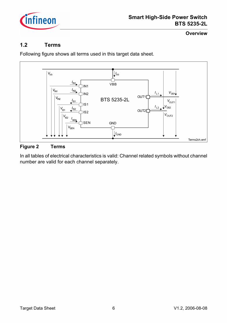
1.2 TermsFollowing figure shows all terms used in this target data sheet.
Figure 2 Terms
In all tables of electrical characteristics is valid: Channel related symbols without channelnumber are valid for each channel separately.
Terms2ch.emf
IIN1
VIN1
OUT1
IIN2
VIN2
VIS1
IIS1
VIS2
IIS2
Vbb
VSEN
ISEN
I L1
VOUT2
VOUT1
VDS2
VDS1
I L2
GND
IGND
Ibb
IN1
IN2
IS1
IS2
SEN
VBB
OUT2
BTS 5235-2L
Target Data Sheet 6 V1.2, 2006-08-08
Smart High-Side Power SwitchBTS 5235-2L
Pin Configuration
Target Data Sheet 7 V1.2, 2006-08-08
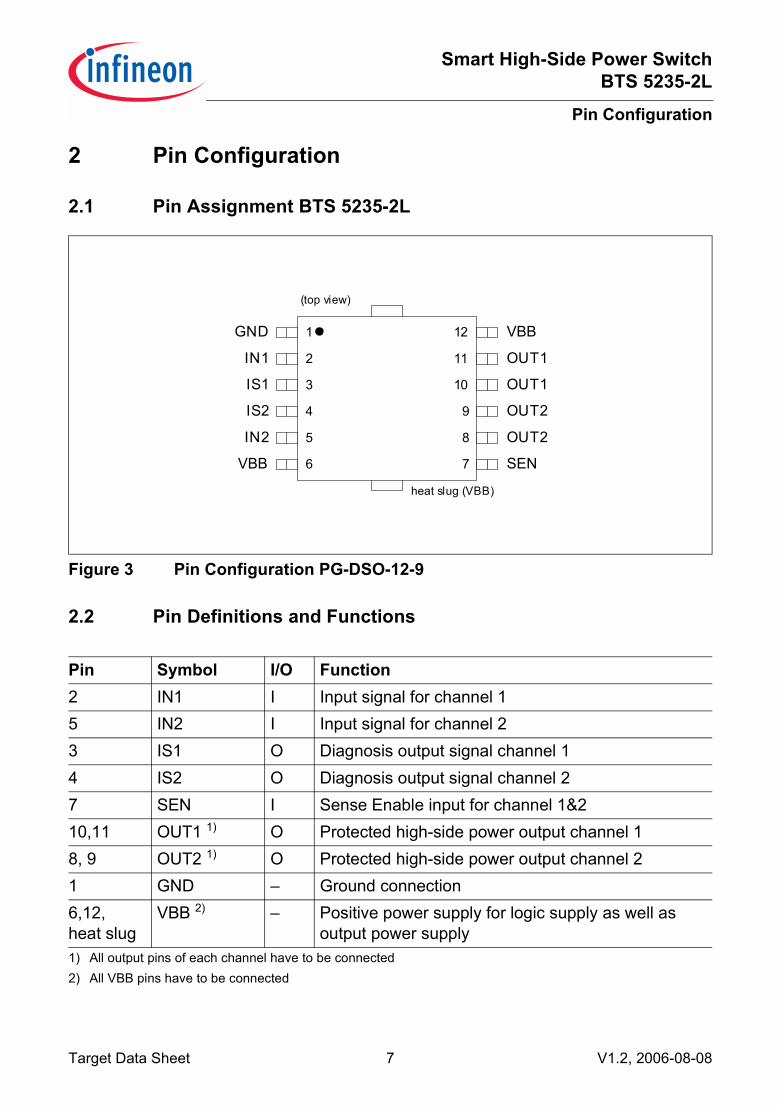
2 Pin Configuration
2.1 Pin Assignment BTS 5235-2L
Figure 3 Pin Configuration PG-DSO-12-9
2.2 Pin Definitions and Functions
Pin Symbol I/O Function2 IN1 I Input signal for channel 15 IN2 I Input signal for channel 23 IS1 O Diagnosis output signal channel 14 IS2 O Diagnosis output signal channel 27 SEN I Sense Enable input for channel 1&210,11 OUT1 1)
1) All output pins of each channel have to be connected
O Protected high-side power output channel 18, 9 OUT2 1) O Protected high-side power output channel 21 GND Ground connection6,12,heat slug
VBB 2)
2) All VBB pins have to be connected
Positive power supply for logic supply as well as output power supply
(top view)
OUT1
OUT1
OUT2
OUT2
VBB
SEN
12
11
10
9
8
7
IN1
IS1
IS2
IN2
GND
VBB
1
2
3
4
5
6
heat slug (VBB)

Smart High-Side Power SwitchBTS 5235-2L
Electrical Characteristics
3 Electrical Characteristics
3.1 Maximum Ratings Stresses above the ones listed here may affect device reliability or may cause permanentdamage to the device.
Unless otherwise specified:Tj = 25 °C
Pos. Parameter Symbol Limit Values Unit Test Conditionsmin. max.
Supply Voltage3.1.1 Supply voltage Vbb -16 28 V3.1.2 Supply voltage for full short
circuit protection (single pulse)(Tj(0) = -40 °C .. 150 °C)
Vbb(SC) 0 28 V L = 8 µH,R = 0.2 Ω 1)
3.1.3 Voltage at power transistor VDS 52 V3.1.4 Supply Voltage for Load Dump
protectionVbb(LD) 41 V RI = 2 Ω 2)
RL = 6.8 ΩPower Stages3.1.5 Load current IL IL(LIM) A 3)
3.1.6 Maximum energy dissipation single pulse
EAS 110 mJ IL(0) = 2 A 4)
Tj(0) = 150 °CVbb=12V
3.1.7 Power dissipation (DC) Ptot 1.6 W Ta = 85 °C 5)
Tj ≤ 150 °C
Logic Pins3.1.8 Voltage at input pin VIN -5
-1610 V
t ≤ 2 min3.1.9 Current through input pin IIN -2.0
-8.02.0 mA
t ≤ 2 min3.1.10 Voltage at sense enable pin VSEN -5
-1610 V
t ≤ 2 min3.1.11 Current through sense enable
pinISEN -2.0
-8.02.0 mA
t ≤ 2 min3.1.12 Current through sense pin IIS -25 10 mA
Target Data Sheet 8 V1.2, 2006-08-08

Smart High-Side Power SwitchBTS 5235-2L
Electrical Characteristics
Temperatures3.1.13 Junction Temperature Tj -40 150 °C3.1.14 Dynamic temperature increase
while switching∆Tj - 60 °C
3.1.15 Storage Temperature Tstg -55 150 °CESD Susceptibility3.1.16 ESD susceptibility HBM
IN, SENIS
OUT
VESD-1-2-4
124
kV according to EIA/JESD 22-A 114B
1) R and L describe the complete circuit impedance including line, contact and generator impedances2) Load Dump is specified in ISO 7636, RI is the internal resistance of the Load Dump pulse generator3) Current limitation is a protection feature. Operation in current limitation is considered as outside normal
operating range. Protection features are not designed for continuous repetitive operation.4) Pulse shape represents inductive switch off: IL(t) = IL(0) * (1 - t / tpulse); 0 < t < tpulse
5) Device mounted on PCB (50 mm × 50 mm × 1.5mm epoxy, FR4) with 6 cm2 copper heatsinking area (onelayer, 70 µm thick) for Vbb connection. PCB is vertical without blown air.
Unless otherwise specified:Tj = 25 °C
Pos. Parameter Symbol Limit Values Unit Test Conditionsmin. max.
Target Data Sheet 9 V1.2, 2006-08-08

Smart High-Side Power SwitchBTS 5235-2L
Block Description and Electrical Characteristics
4 Block Description and Electrical Characteristics
4.1 Power StagesThe power stages are built by N-channel vertical power MOSFETs (DMOS) with chargepumps.
4.1.1 Output On-State ResistanceThe on-state resistance RDS(ON) depends on the supply voltage as well as the junctiontemperature Tj. Figure 4 shows that dependencies for the typical on-state resistance.The behavior in reverse polarity mode is described in Section 4.2.2.
Figure 4 Typical On-State Resistance
4.1.2 Input CircuitFigure 5 shows the input circuit of the BTS 5235-2L. There is an integrated input resistorthat makes external components obsolete. The current sink to ground ensures that thedevice switches off in case of open input pin. The zener diode protects the input circuitagainst ESD pulses.
Figure 5 Input Circuit (IN1 and IN2)
30
40
50
60
70
80
90
-50 -25 0 25 50 75 100 125 150
RD
S(O
N) /
mΩ
T /°C
40
60
80
100
120
140
160
0 5 10 15 20 25
RD
S(O
N) /
mΩ
Vbb /V
Vbb = 13.5 V Tj = 25 °C
IN RIN
IIN
GND
RGND
Input.emf
Target Data Sheet 10 V1.2, 2006-08-08

Smart High-Side Power SwitchBTS 5235-2L
Block Description and Electrical Characteristics
A high signal at the input pin causes the power DMOS to switch on with a dedicatedslope, which is optimized in terms of EMC emission.
Figure 6 Switching a Load (resistive)
4.1.3 Inductive Output ClampWhen switching off inductive loads with high-side switches, the voltage VOUT drops belowground potential, because the inductance intends to continue driving the current.
Figure 7 Output Clamp (OUT1 and OUT2)
To prevent destruction of the device, there is a voltage clamp mechanism implementedthat keeps that negative output voltage at a certain level (VOUT(CL)). See Figure 7 andFigure 8 for details. Nevertheless, the maximum allowed load inductance is limited.
IN
VOUT
t
SwitchOn.emf
tON tOFF
t
90%
10%
70%
dV /dtON
30%
70%
dV /dtOFF
30%
OutputClamp.emf
OUTGND
VbbVBB
L,RL
VOUT
I L
Target Data Sheet 11 V1.2, 2006-08-08

Smart High-Side Power SwitchBTS 5235-2L
Block Description and Electrical Characteristics
Figure 8 Switching an Inductance
Maximum Load InductanceWhile demagnetization of inductive loads, energy has to be dissipated in the BTS 5235-2L. This energy can be calculated with following equation:
[1]
This equation simplifies under the assumption of RL = 0:
[2]
The energy, which is converted into heat, is limited by the thermal design of thecomponent. See Figure 9 for the maximum allowed energy dissipation.
VOUT
InductiveLoad.emf
t
IL
t
VOUT(CL)
Vbb
IN = 5V IN = 0V
0
E Vbb VOUT(CL)( )VOUT(CL)
RL----------------------- ln⋅ 1
RL IL⋅VOUT(CL)-----------------------
IL+ LRL------⋅ ⋅=
E 12---LIL
2 1Vbb
VOUT(CL)-----------------------
⋅=
Target Data Sheet 12 V1.2, 2006-08-08
Smart High-Side Power SwitchBTS 5235-2L
Block Description and Electrical Characteristics
Figure 9 Maximum Energy Dissipation Single Pulse, Tj,Start = 150 °C
To be added after characterization of first samples
Target Data Sheet 13 V1.2, 2006-08-08

Smart High-Side Power SwitchBTS 5235-2L
Block Description and Electrical Characteristics
4.1.4 Electrical Characteristics
Unless otherwise specified:Vbb = 9 V to 16 V, Tj = -40 °C to +150 °C, typical values: Vbb = 13.5 V, Tj = 25 °C
Pos. Parameter Symbol Limit Values Unit Test Conditionsmin. typ. max.
General4.1.1 Operating voltage Vbb 4.5 28 V VIN = 4.5 V
RL = 12 ΩVDS < 0.5 V
4.1.2 Operating currentone channel activeall channels active
IGND1.83.6
4.08.0
mA VIN = 5 V
4.1.3 Standby current for whole device with load
Ibb(OFF)
1.5 2.5 2.5 15
µA VIN = 0 VVSEN = 0 VTj = 25 °CTj = 85 °C1)
Tj = 150 °COutput Characteristics4.1.4 On-State resistance
per channelRDS(ON)
4590
60115
mΩ IL = 2.5 A Tj = 25 °C Tj = 150 °C
4.1.5 Output voltage drop limitation at small load currents
VDS(NL) 40 mV IL < 0.25 A
4.1.6 Nominal load current per channel
one channel activetwo channels active
IL(nom)
3.5 2.6
A Ta = 85 °CTj ≤ 150 °C 2) 3)
ISO load current per channel
one channel activetwo channels active
IL(ISO)
5.35.3
A Tc = 85 °C VDS = 0.5 V 3)
4.1.7 Output clamp VOUT(CL) -24 -20 -17 V IL = 40 mA4.1.8 Output leakage
current per channelIL(OFF) 0.1 6.0 µA VIN = 0 V
4.1.9 Inverse current capability
-IL(inv) 3 A 1)
Target Data Sheet 14 V1.2, 2006-08-08
Smart High-Side Power SwitchBTS 5235-2L
Block Description and Electrical Characteristics
Note: Characteristics show the deviation of parameter at the given supply voltage andjunction temperature. Typical values show the typical parameters expected frommanufacturing.
Thermal Resistance4.1.10 Junction to case Rthjc 2.2 K/W 1)
4.1.11 Junction to ambient one channel activeall channels active
Rthja45 40
K/W 1) 2)
Input Characteristics4.1.12 Input resistor RIN 1.8 3.5 5.5 kΩ4.1.13 L-input level VIN(L) -0.3 1.0 V4.1.14 H-input level VIN(H) 2.5 5.7 V4.1.15 L-input current IIN(L) 3 18 75 µA VIN = 0.4 V4.1.16 H-input current IIN(H) 10 38 75 µA VIN = 5 VTimings4.1.17 Turn-on time to
90% Vbb
tON 100 250 µs RL = 12 ΩVbb = 13.5 V
4.1.18 Turn-off time to 10% Vbb
tOFF 120 250 µs RL = 12 ΩVbb = 13.5 V
4.1.19 slew rate 30% to 70% Vbb
dV/ dtON 0.1 0.25 0.5 V/µs RL = 12 ΩVbb = 13.5 V
4.1.20 slew rate 70% to 30% Vbb
-dV/ dtOFF
0.1 0.25 0.5 V/µs RL = 12 ΩVbb = 13.5 V
1) Not subject to production test, specified by design2) Device mounted on PCB (50 mm × 50 mm × 1.5mm epoxy, FR4) with 6 cm2 copper heatsinking area (one
layer, 70 µm thick) for Vbb connection. PCB is vertical without blown air.3) Not subject to production test, parameters are calculated from RDS(ON) and Rth
Unless otherwise specified:Vbb = 9 V to 16 V, Tj = -40 °C to +150 °C, typical values: Vbb = 13.5 V, Tj = 25 °C
Pos. Parameter Symbol Limit Values Unit Test Conditionsmin. typ. max.
Target Data Sheet 15 V1.2, 2006-08-08
Smart High-Side Power SwitchBTS 5235-2L
4.2 Protection FunctionsThe device provides embedded protective functions. Integrated protection functions aredesigned to prevent IC destruction under fault conditions described in the data sheet.Fault conditions are considered as outside normal operating range. Protectionfunctions are neither designed for continuous nor repetitive operation.
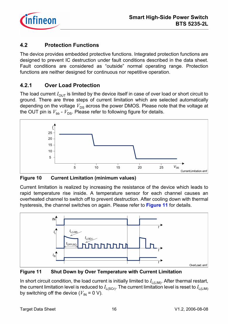
4.2.1 Over Load ProtectionThe load current IOUT is limited by the device itself in case of over load or short circuit toground. There are three steps of current limitation which are selected automaticallydepending on the voltage VDS across the power DMOS. Please note that the voltage atthe OUT pin is Vbb - VDS. Please refer to following figure for details.
Figure 10 Current Limitation (minimum values)
Current limitation is realized by increasing the resistance of the device which leads torapid temperature rise inside. A temperature sensor for each channel causes anoverheated channel to switch off to prevent destruction. After cooling down with thermalhysteresis, the channel switches on again. Please refer to Figure 11 for details.
Figure 11 Shut Down by Over Temperature with Current Limitation
In short circuit condition, the load current is initially limited to IL(LIM). After thermal restart,the current limitation level is reduced to IL(SCr). The current limitation level is reset to IL(LIM)by switching off the device (VIN = 0 V).
CurrentLimitation.emf
IL
5 10 15 20
5
10
15
20
25
VDS25
IN
IL
IIS
t
IL(LIM)
IL(SCr)
t
t
OverLoad.emf
tOFF(SC)
Target Data Sheet 16 V1.2, 2006-08-08

Smart High-Side Power SwitchBTS 5235-2L
4.2.2 Reverse Polarity ProtectionIn case of reverse polarity, the intrinsic body diode causes power dissipation. Additionalpower is dissipated by the integrated ground resistor. Use following formula forestimation of total power dissipation Pdiss(rev) in reverse polarity mode.
[3]
The reverse current through the intrinsic body diode has to be limited by the connectedload. The current through sense pins IS1 and IS2 has to be limited (please refer tomaximum ratings on Page 8). The current through the ground pin (GND) is limitedinternally by RGND. The over-temperature protection is not active during reverse polarity.
4.2.3 Over Voltage ProtectionIn addition to the output clamp for inductive loads as described in Section 4.1.3, there isa clamp mechanism for over voltage protection. Because of the integrated groundresistor, over voltage protection does not require external components.As shown in Figure 12, in case of supply voltages greater than Vbb(AZ), the powertransistor switches on and the voltage across logic part is clamped. As a result, theinternal ground potential rises to Vbb - Vbb(AZ). Due to the ESD zener diodes, the potentialat pin IN1, IN2 and SEN rises almost to that potential, depending on the impedance ofthe connected circuitry.
Figure 12 Over Voltage Protection
4.2.4 Loss of Ground ProtectionIn case of complete loss of the device ground connections, but connected load ground,the BTS 5235-2L securely changes to or stays in off state.
Pdiss(rev) VDS(rev) IL⋅( )all channels∑
Vbb2
RGND--------------+=
OUT
VBB
OverVoltage .emf
VOUTRGND
logic
GND
IN
IS
SEN RSEN
RIN
ZDESD
ZDAZ
internal ground
Target Data Sheet 17 V1.2, 2006-08-08

Smart High-Side Power SwitchBTS 5235-2L
4.2.5 Electrical Characteristics
Unless otherwise specified:Vbb = 9 V to 16 V, Tj = -40 °C to +150 °C , typical values: Vbb = 13.5 V, Tj = 25 °C
Pos. Parameter Symbol Limit Values Unit Test Conditionsmin. typ. max.
Over Load Protection4.2.1 Load current limitation IL(LIM) 23 42 A VDS = 7 V
14 28 A VDS = 14 V3 14 A VDS = 28 V 1) 2)
1) Please note that an external forced VDS must not exceed Vbb + |VOUT(CL)|
4.2.2 Repetitive short circuit current limitation
IL(SCr) 6 A Tj = Tj(SC) 2)
2) Not subject to production test, specified by design
4.2.3 Initial short circuit shut down time
tOFF(SC) 0.8 ms TjStart = 25 °C 2)
4.2.4 Thermal shut down temperature
Tj(SC) 150 1702)
°C
4.2.5 Thermal hysteresis ∆Tj 7 K 2)
Reverse Battery4.2.6 Drain-Source diode
voltage (VOUT > Vbb)-VDS(rev) 900 mV IL = -3.5 A
Vbb = -13.5 VTj = 150 °C
4.2.7 Reverse current through GND pin
-IGND 65 mA Vbb = -13.5 V 2)
Ground Circuit4.2.8 Integrated Resistor in
GND lineRGND 115 220 350 Ω
Over Voltage4.2.9 Over voltage
protectionVbb(AZ) 41 47 53 V Ibb = 2 mA
Loss of GND4.2.10 Output leakage
current while GND disconnected
IL(GND) 1 mA IIN = 0, ISEN = 0, IIS = 0, IGND = 0 2) 3)
3) No connection at these pins
Target Data Sheet 18 V1.2, 2006-08-08
Smart High-Side Power SwitchBTS 5235-2L
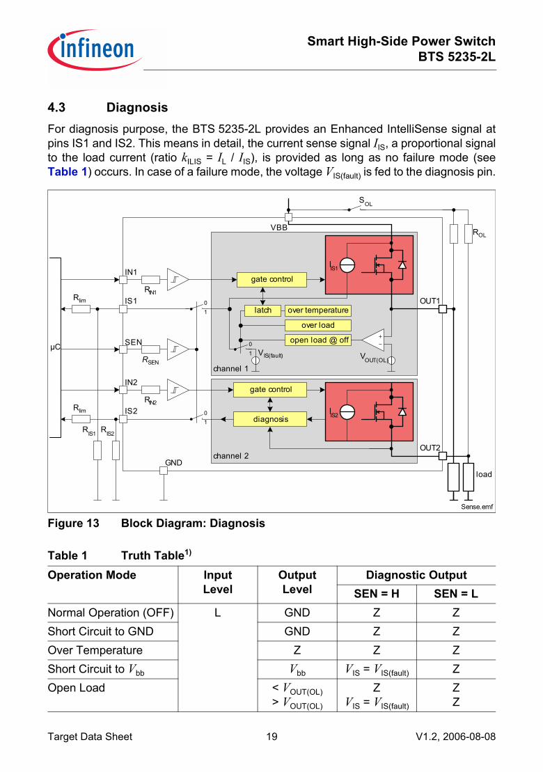
4.3 DiagnosisFor diagnosis purpose, the BTS 5235-2L provides an Enhanced IntelliSense signal atpins IS1 and IS2. This means in detail, the current sense signal IIS, a proportional signalto the load current (ratio kILIS = IL / IIS), is provided as long as no failure mode (seeTable 1) occurs. In case of a failure mode, the voltage VIS(fault) is fed to the diagnosis pin.
Figure 13 Block Diagram: Diagnosis
Table 1 Truth Table1)
Operation Mode Input Level
Output Level
Diagnostic OutputSEN = H SEN = L
Normal Operation (OFF) L GND Z ZShort Circuit to GND GND Z ZOver Temperature Z Z ZShort Circuit to Vbb Vbb VIS = VIS(fault) ZOpen Load < VOUT(OL)
> VOUT(OL)
Z VIS = VIS(fault)
ZZ
channel 1
channel 2
IIS2
OUT2
IIS1
OUT1IS1
µC
IN1
VOUT(OL)
01 VIS(fault)
RIN1
gate control
IN2
IS2diagnosis
GND
ROL
SOL
load
VBB
Sense.emf
RIS1 RIS2
Rlim
Rlim
over temperature
over load
gate controlRIN2
open load @ offSEN
01
RSEN
01
latch
Target Data Sheet 19 V1.2, 2006-08-08

Smart High-Side Power SwitchBTS 5235-2L
4.3.1 ON-State DiagnosisThe standard diagnosis signal is a current sense signal proportional to the load current.The accuracy of the ratio (kILIS = IL / IIS) depends on the temperature. Please refer tofollowing Figure 14 for details. Usually a resistor RIS is connected to the current sensepin. It is recommended to use sense resistors RIS > 500 Ω. A typical value is 4.7 kΩ.
Figure 14 Current sense ratio kILIS1)
Normal Operation (ON) H ~Vbb IIS = IL / kILIS ZCurrent Limitation < Vbb VIS = VIS(fault) ZShort Circuit to GND ~GND VIS = VIS(fault) ZOver Temperature Z VIS = VIS(fault) ZShort Circuit to Vbb Vbb IIS < IL / kILIS ZOpen Load Vbb Z Z1) L = Low Level, H = High Level, Z = high impedance, potential depends on leakage currents and external circuit
1) The curves show the behavior based on characterization data. The marked points are guaranteed in thisTarget Data Sheet in Section 4.3.4 (Position 4.3.6).
Table 1 Truth Table1) (contd)
Operation Mode Input Level
Output Level
Diagnostic OutputSEN = H SEN = L
1000
2000
3000
4000
5000
6000
7000
8000
0 0.5 1 1.5 2 2.5 3 3.5 4
k ILI
S
IL /A
dummyTj = 150°C
dummyTj = -40°C
Target Data Sheet 20 V1.2, 2006-08-08

Smart High-Side Power SwitchBTS 5235-2L
Details about timings between the diagnosis signal IIS and the output voltage VOUT andload current IL in ON-state can be found in Figure 15.
Figure 15 Timing of Diagnosis Signal in ON-state
In case of over-load as well as over-temperature, the voltage VIS(fault) is fed to thediagnosis pins as long as the according input pin is high. This means, even if theoverload disappears after the first thermal shutdown or when the device keeps switchingon and off in over-load condition (thermal toggling), the diagnosis signal(VIS(fault)) isconstantly available. Please refer to Figure 16 for details. Please note, that if theoverload disapears before the first thermal shutdown, the diagnosis signal (VIS(fault)) mayremain for approximately 300 µs longer than the duration of the overload.As a result open load and over load including over temperature can be differentiated inON-state.Consideration must be taken in the selection of the sense resistor in order to distinguishnominal currents from the overload/short circuit fault state. A potential of 5 V at the sensepin can be achieved with a big sense resistor even with currents being much smaller thanthe current limitation.
SwitchOn.emf
IN
VOUT
IIS
t
t
t
ILt
ON
tON
tsIS(ON) tsIS(LC)
OFF
normal operation over load (current limitation)
tsIS(OVL)
VIS(fault) / RS
Target Data Sheet 21 V1.2, 2006-08-08

Smart High-Side Power SwitchBTS 5235-2L
Figure 16 Timing of Diagnosis Signal in Over Load Condition
4.3.2 OFF-State DiagnosisDetails about timings between the diagnosis signal IIS and the output voltage VOUT andload current IL in OFF-state can be found in Figure 17. For open load diagnosis in OFF-state an external output pull-up resistor (ROL) is necessary.
Figure 17 Timing of Diagnosis Signal in OFF-state
For calculation of the pull-up resistor, just the external leakage current Ileakage and theopen load threshold voltage VOUT(OL) has to be taken into account.
[4]
Ileakage defines the leakage current in the complete system e.g. caused by humidity.There is no internal leakage current from out to ground at BTS 5235-2L. Vbb(min) is theminimum supply voltage at which the open load diagnosis in off state must be ensured.To reduce the stand-by current of the system, an open load resistor switch (SOL) isrecommended.
OverLoad.emf
IN
IIS
t
t
IL
ON
tsIS(OVL)
OFF
VIS(fault) / RS
over temperatureover load (current limitation)
OFF
IL(LIM)
SwitchOff.emf
IN
VOUT
IIS
t
t
t
Open Load, pull-up resistor active
VIS(fault) / RS
ON OFF
td(fault) ts(fault)
pull-up resistorinactive
ROLVbb(min) VOUT(OL,max)
Ileakage-----------------------------------------------------------=
Target Data Sheet 22 V1.2, 2006-08-08

Smart High-Side Power SwitchBTS 5235-2L
4.3.3 Sense Enable FunctionThe diagnosis signals have to be switched on by a high signal at sense enable pin (SEN).See Figure 18 for details on the timing between SEN pin and diagnosis signal IIS. Pleasenote that the diagnosis is disabled, when no signal is provided at pin SEN.
Figure 18 Timing of Sense Enable Signal
The SEN pin circuit is designed equally to the input pin. Please refer to Figure 5 fordetails. The resistors Rlim are recommended to limit the current through the sense pinsIS1 and IS2 in case of reverse polarity and over voltage. Please refer to maximum ratingson Page 8.The stand-by current of the BTS 5235-2L is minimized, when both input pins (IN1 andIN2) and the sense enable pin (SEN) are on low level.
tdIS(SEN)tsIS(SEN)t
SEN.emf
tsIS(SEN)
t
tdIS(SEN)IIS
SEN
Target Data Sheet 23 V1.2, 2006-08-08

Smart High-Side Power SwitchBTS 5235-2L
4.3.4 Electrical Characteristics
Unless otherwise specified:Vbb = 9 V to 16 V, Tj = -40 °C to +150 °C, VSEN = 5 V, typical values: Vbb = 13.5 V, Tj = 25 °C
Pos. Parameter Symbol Limit Values Unit Test Conditionsmin. typ. max.
General Definition4.3.1 Diagnostics signal in
failure modeVIS(fault) 5 9 V VIN = 0 V
VOUT = VbbIIS = 1 mA
4.3.2 Diagnostics signal current limitation in failure mode
IIS(LIM) 3 mA VIN = 0 VVOUT = Vbb
Open Load at OFF-State4.3.3 Open load detection
threshold voltageVOUT(OL) 1.6 2.8 4.4 V
4.3.4 Sense signal invalid after negative input slope
td(fault) 1.2 ms VIN = 5 V to 0 VVOUT = Vbb
4.3.5 Fault signal settling time
ts(fault) 200 µs VIN = 0 VVOUT = 0 V to
> VOUT(OL)IIS = 1 mA
Load Current Sense ON-State4.3.6 Current sense ratio kILIS 2870 VIN = 5 V
IL = 40 mAIL = 1.3 AIL = 2.2 AIL = 4.0 A
1000230024102465
4035305029202850
8000358033803275
Tj = -40 °C
IL = 40 mAIL = 1.3 AIL = 2.2 AIL = 4.0 A
1400246525202580
3410292028752870
6000327532203160
Tj = 150 °C
4.3.7 Current sense voltage limitation
VIS(LIM) 5.0 6.2 7.5 V IIS = 0.5 mAIL = 3.5 A
4.3.8 Current sense leakage/offset current
IIS(LH) 3.5 µA VIN = 5 VIL = 0 A
Target Data Sheet 24 V1.2, 2006-08-08

Smart High-Side Power SwitchBTS 5235-2L
4.3.9 Current sense leakage, while diagnosis disabled
IIS(dis) 1 µA VSEN = 0 VIL = 3.5 A
4.3.10 Current sense settling time to IIS static ±10% after positive input slope
tsIS(ON) 350 µs VIN = 0 V to 5 VIL = 3.5 A
1)
4.3.11 Current sense settling time to IIS static ±10% after change of load current
tsIS(LC) 50 µs VIN = 5 VIL = 1.3 A to 2.2 A
1)
Over Load in ON-State4.3.12 Over load detection
currentIL(OVL) 8 IL(LIM) A VIN = 5 V
VIS = VIS(fault)1)
4.3.13 Sense signal settling time in overload condition
tsIS(OVL) 200 µs VOUT = 2 VVIN = 0 V to 5 V
Sense Enable4.3.14 Input resistance RSEN 1.8 3.5 5.5 kΩ4.3.15 L-input level VSEN(L) -0.3 1.0 V4.3.16 H-input level VSEN(H) 2.5 5.7 V4.3.17 L-input current ISEN(L) 3 18 75 µA VSEN = 0.4 V4.3.18 H-input current ISEN(H) 10 38 75 µA VSEN = 5 V4.3.19 Current sense settling
timetsIS(SEN) 3 25 µs VSEN = 0 V to 5 V
VIN = 0 VVOUT > VOUT(OL)
4.3.20 Current sense deactivation time
tdIS(SEN) 25 µs VSEN = 5 V to 0 VIL = 3.5 ARS = 5 kΩ 1)
1) Not subject to production test, specified by design
Unless otherwise specified:Vbb = 9 V to 16 V, Tj = -40 °C to +150 °C, VSEN = 5 V, typical values: Vbb = 13.5 V, Tj = 25 °C
Pos. Parameter Symbol Limit Values Unit Test Conditionsmin. typ. max.
Target Data Sheet 25 V1.2, 2006-08-08

Smart High-Side Power SwitchBTS 5235-2L
Package Outlines BTS 5235-2L
Target Data Sheet 26 V1.2, 2006-08-08
5 Package Outlines BTS 5235-2L
Figure 19 PG-DSO-12-9 (Plastic Dual Small Outline Package)
To meet the world-wide customer requirements for environmentally friendly products and to becompliant with government regulations the device is available as a green product. Green productsare RoHS-Compliant (i.e Pb-free finish on leads and suitable for Pb-free soldering according to IPC/JEDEC J-STD-020).Please specify the package needed (e.g. green package) when placing an order
1 6
712
0.8
(1.5
5)
2.35
±0.1
0.1±
0.05
3)
2.6
MA
X.
C0.1
±0.310.3
(4.4)4.
2±0
.1
(1.8
)±0.1
1.6
ø0.8 x 0.1 -0.05 Depth 4)
+0.130.4
1
5 x 1 = 5
C0.25 M A B
±0.15.1
6.4A
±0.1 7.5B
±0.1
7.8 ±0.1
(Heatslug)
0.25 B
(0.2)
0.7 ±0.15
+0.0
750.
25-0
.035
5˚±3
˚
8˚ 8˚
0.1 12x
1)
Seating Plane+0
.10
2)
Does not include plastic or metal protrusion of 0.15 max. per sideStand OFF
Pin 1 Index Marking; Polish finishStand OUT
All package corners max. R 0.25
1)
2)
3)
4)
1)
C
Dimensions in mm
You can find all of our packages, sorts of packing and others in our Infineon Internet Page Products: http://www.infineon.com/products.

Smart High-Side Power SwitchBTS 5235-2L
Revision History
Target Data Sheet 27 2006-08-08
6 Revision History
Version Date ChangesV1.1 06-08-08 Creation of the green target datasheet.
Delta sheet to the grey datasheet BTS5235L datasheet of the December 19th 2005 version 1.0 :parameter 3.1.6 : change to 110mJ at 12VFigure 9 set to tbdparameter 4.1.7 : -24V min, -17V max
Edition 2006-08-08Published by Infineon Technologies AG,St.-Martin-Strasse 53,D-81541 München, Germany© Infineon Technologies AG 8/22/06.All Rights Reserved.
Attention please!The information herein is given to describe certain components and shall not be considered as warranted characteristics.Terms of delivery and rights to technical change reserved.We hereby disclaim any and all warranties, including but not limited to warranties of non-infringement, regarding circuits, descriptions and charts stated herein.Infineon Technologies is an approved CECC manufacturer.
InformationFor further information on technology, delivery terms and conditions and prices please contact your nearest Infineon Technologies Office in Germany or our Infineon Technologies Representatives worldwide.
WarningsDue to technical requirements components may contain dangerous substances. For information on the types in question please contact your nearest Infineon Technologies Office.Infineon Technologies Components may only be used in life-support devices or systems with the express written approval of Infineon Technologies, if a failure of such components can reasonably be expected to cause the failure of that life-support device or system, or to affect the safety or effectiveness of that device or system. Life support devices or systems are intended to be implanted in the human body, or to support and/or maintain and sustain and/or protect human life. If they fail, it is reasonable to assume that the health of the user or other persons may be endangered.
Smart High-Side Power SwitchBTS 5235-2L
Target Data Sheet 28 2006-08-08

h t t p : / / w w w . i n f i n e o n . c o m
Published by Infineon Technologies AG