BTS5x34Data Sheet 3 V1.0, 2004-01-23 Type Ordering Code Package BTS 5234L Q67060-S6155 P-DSO-12-2...
28
Data Sheet, V1.0, January 2004 Never stop thinking. BTS 5234L Smart High-Side Power Switch PROFET Two Channels, 60 m Ω Automotive Power
Transcript of BTS5x34Data Sheet 3 V1.0, 2004-01-23 Type Ordering Code Package BTS 5234L Q67060-S6155 P-DSO-12-2...

Data Sheet, V1.0, January 2004
N e v e r s t o p t h i n k i n g .
BTS 5234LSmart High-Side Power Switch
PROFET
Two Channels, 60 mΩ
Automotive Power

Smart High-Side Power SwitchBTS 5234L
Table of Contents Page
Data Sheet 2 V1.0, 2004-01-23
Product Summary . . . . . . . . . . . . . . . . . . . . . . . . . . . . . . . . . . . . . . . . . . . . . . . . . . . .3
1 Overview . . . . . . . . . . . . . . . . . . . . . . . . . . . . . . . . . . . . . . . . . . . . . . . . . . . . . . . . .51.1 Block Diagram . . . . . . . . . . . . . . . . . . . . . . . . . . . . . . . . . . . . . . . . . . . . . . . . . . .51.2 Terms . . . . . . . . . . . . . . . . . . . . . . . . . . . . . . . . . . . . . . . . . . . . . . . . . . . . . . . . .6
2 Pin Configuration . . . . . . . . . . . . . . . . . . . . . . . . . . . . . . . . . . . . . . . . . . . . . . . . . .72.1 Pin Assignment BTS 5234L . . . . . . . . . . . . . . . . . . . . . . . . . . . . . . . . . . . . . . . . .72.2 Pin Definitions and Functions . . . . . . . . . . . . . . . . . . . . . . . . . . . . . . . . . . . . . . .7
3 Electrical Characteristics . . . . . . . . . . . . . . . . . . . . . . . . . . . . . . . . . . . . . . . . . . . .83.1 Maximum Ratings . . . . . . . . . . . . . . . . . . . . . . . . . . . . . . . . . . . . . . . . . . . . . . . .8
4 Block Description and Electrical Characteristics . . . . . . . . . . . . . . . . . . . . . . .104.1 Power Stages . . . . . . . . . . . . . . . . . . . . . . . . . . . . . . . . . . . . . . . . . . . . . . . . . .10
4.1.1 Output On-State Resistance . . . . . . . . . . . . . . . . . . . . . . . . . . . . . . . . . . 104.1.2 Input Circuit . . . . . . . . . . . . . . . . . . . . . . . . . . . . . . . . . . . . . . . . . . . . . . . 104.1.3 Inductive Output Clamp . . . . . . . . . . . . . . . . . . . . . . . . . . . . . . . . . . . . . . 114.1.4 Electrical Characteristics . . . . . . . . . . . . . . . . . . . . . . . . . . . . . . . . . . . . 13
4.2 Protection Functions . . . . . . . . . . . . . . . . . . . . . . . . . . . . . . . . . . . . . . . . . . . . .154.2.1 Over Load Protection . . . . . . . . . . . . . . . . . . . . . . . . . . . . . . . . . . . . . . . . 154.2.2 Reverse Polarity Protection . . . . . . . . . . . . . . . . . . . . . . . . . . . . . . . . . . . 164.2.3 Over Voltage Protection . . . . . . . . . . . . . . . . . . . . . . . . . . . . . . . . . . . . . 164.2.4 Loss of Ground Protection . . . . . . . . . . . . . . . . . . . . . . . . . . . . . . . . . . . . 164.2.5 Electrical Characteristics . . . . . . . . . . . . . . . . . . . . . . . . . . . . . . . . . . . . 17
4.3 Diagnosis . . . . . . . . . . . . . . . . . . . . . . . . . . . . . . . . . . . . . . . . . . . . . . . . . . . . . .184.3.1 ON-State Diagnosis . . . . . . . . . . . . . . . . . . . . . . . . . . . . . . . . . . . . . . . . . 194.3.2 OFF-State Diagnosis . . . . . . . . . . . . . . . . . . . . . . . . . . . . . . . . . . . . . . . . 204.3.3 Sense Enable Function . . . . . . . . . . . . . . . . . . . . . . . . . . . . . . . . . . . . . . 214.3.4 Electrical Characteristics . . . . . . . . . . . . . . . . . . . . . . . . . . . . . . . . . . . . 22
5 Package Outlines BTS 5234L . . . . . . . . . . . . . . . . . . . . . . . . . . . . . . . . . . . . . . . .24
6 Revision History . . . . . . . . . . . . . . . . . . . . . . . . . . . . . . . . . . . . . . . . . . . . . . . . . .25

Smart High-Side Power SwitchPROFET
BTS 5234L
Product Summary
The BTS 5234L is a dual channel high-side power switch in P-DSO-12-2 package providing embedded protective functions.
The power transistor is built by a N-channel vertical power MOSFET with charge pump. The device is monolithically integrated in Smart SIPMOS technology.
Basic Features
• Very low standby current• 3.3 V and 5 V compatible logic pins• Improved electromagnetic compatibility (EMC)• Stable behavior at under voltage• Logic ground independent from load ground• Secure load turn-off while logic ground disconnected• Optimized inverse current capability
Operating voltage Vbb(on) 4.5 .. 28 V
Over voltage protection Vbb(AZ) 41 V
On-State resistance RDS(ON) 60 mΩNominal load current (one channel active) IL(nom) 3.5 A
Current limitation IL(LIM) 23 A
Current limitation repetitive IL(SCr) 6 A
Standby current for whole device with load Ibb(OFF) 2.5 µA
P-DSO-12-2
Data Sheet 3 V1.0, 2004-01-23
Type Ordering Code Package
BTS 5234L Q67060-S6155 P-DSO-12-2

Smart High-Side Power SwitchBTS 5234L
Protective Functions
• Reverse battery protection without external components• Short circuit protection• Overload protection • Multi-step current limitation• Thermal shutdown with restart• Thermal restart at reduced current limitation• Over voltage protection without external resistor• Loss of ground protection• Electrostatic discharge protection (ESD)
Diagnostic Functions
• Enhanced IntelliSense signal for each channel• Enable function for diagnosis pins (IS1 and IS2)• Proportional load current sense signal by current source• High accuracy of current sense signal at wide load current range• Open load detection in ON-state by load current sense• Open load detection in OFF-state by voltage source• Feedback on over temperature and current limitation in ON-state
Applications
• µC compatible high-side power switch with diagnostic feedback for 12 V groundedloads
• All types of resistive, inductive and capacitive loads• Suitable for loads with high inrush currents, so as lamps• Suitable for loads with low currents, so as LEDs• Replaces electromechanical relays, fuses and discrete circuits
Data Sheet 4 V1.0, 2004-01-23

Smart High-Side Power SwitchBTS 5234L
Overview
1 OverviewThe BTS 5234L is a dual channel high-side power switch (two times 60 mΩ) inP-DSO-12-2 power package providing embedded protective functions.
The Enhanced IntelliSense pins IS1 and IS2 provide a sophisticated diagnostic feedbacksignal including current sense function and open load in off state. The diagnosis signalscan be switched on and off by the sense enable pin SEN.
An integrated ground resistor as well as integrated resistors at each input pin (IN1, IN2,SEN) reduce external components to a minimum.
The power transistor is built by a N-channel vertical power MOSFET with charge pump. The inputs are ground referenced CMOS compatible. The device is monolithicallyintegrated in Smart SIPMOS technology.
1.1 Block Diagram
Figure 1 Block Diagram
channel 1
internalpowersupply
ESDprotection
OUT2
channel 2control and protection circuit
equivalent tochannel 1
IN1
IS1
SEN
GND
RGND
IS2
IN2
open loaddetection
logic
gate control&
charge pump
VBB
OUT1
clamp forinductive load
multi stepload current
limitation
load currentsense
temperaturesensor
Data Sheet 5 V1.0, 2004-01-23

Smart High-Side Power SwitchBTS 5234L
Overview
1.2 Terms
Following figure shows all terms used in this data sheet.
Figure 2 Terms
Terms2ch.emf
IIN1
VIN1
OUT1
IIN2
VIN2
VIS1
IIS1
VIS2
IIS2
Vbb
VSEN
ISEN
I L1
VOUT2
VOUT1
VDS2
VDS1
I L2
GND
IGND
Ibb
IN1
IN2
IS1
IS2
SEN
VBB
OUT2
BTS 5234L
Data Sheet 6 V1.0, 2004-01-23

Smart High-Side Power SwitchBTS 5234L
Pin Configuration
Data Sheet 7 V1.0, 2004-01-23
2 Pin Configuration
2.1 Pin Assignment BTS 5234L
Figure 3 Pin Configuration P-DSO-12-2
2.2 Pin Definitions and Functions
Pin Symbol I/OOD
Function
2 IN1 I Input signal for channel 1
5 IN2 I Input signal for channel 2
3 IS1 O Diagnosis output signal channel 1
4 IS2 O Diagnosis output signal channel 2
7 SEN I Sense Enable input for channel 1&2
10,11 OUT1 O Protected high-side power output channel 1
8, 9 OUT2 O Protected high-side power output channel 2
1 GND - Ground connection
6,12,heat slug
VBB - Positive power supply for logic supply as well as output power supply
(top view)
OUT1
OUT1
OUT2
OUT2
VBB
SEN
12
11
10
9
8
7
IN1
IS1
IS2
IN2
GND
VBB
1
2
3
4
5
6
heat slug (VBB)

Smart High-Side Power SwitchBTS 5234L
Electrical Characteristics
3 Electrical Characteristics
3.1 Maximum Ratings
Stresses above the ones listed here may affect device reliability or may cause permanentdamage to the device.
Unless otherwise specified:Tj = 25 °C
Pos. Parameter Symbol Limit Values Unit Test Conditionsmin. max.
Supply Voltage
3.1.1 Supply voltage Vbb -16 28 V
3.1.2 Supply voltage for full short circuit protection (single pulse)(Tj(0) = -40°C .. 150°C)
Vbb(SC) 0 28 V L = 8 µH,R = 0.2 Ω 1)
3.1.3 Voltage at power transistor VDS - 52 V
3.1.4 Supply Voltage for Load Dump protection
Vbb(LD) 41 V RI = 2 Ω 2)
RL = 6.8 Ω
Power Stages
3.1.5 Load current IL - IL(LIM) A - 3)
3.1.6 Maximum energy dissipation single pulse
EAS - 0.65 J IL(0) = 2 A 4)
Tj(0) = 150°C
3.1.7 Power dissipation (DC) Ptot - 1.6 W Ta = 85 °C 5)
Tj ≤ 150 °C
Logic Pins
3.1.8 Voltage at input pin VIN -5-16
10 Vt ≤ 2 min
3.1.9 Current through input pin IIN -2.0-8.0
2.0 mAt ≤ 2 min
3.1.10 Voltage at sense enable pin VSEN -5-16
10 Vt ≤ 2 min
3.1.11 Current through sense enable pin
ISEN -2.0-8.0
2.0 mAt ≤ 2 min
3.1.12 Current through sense pin IIS -25 10 mA
Data Sheet 8 V1.0, 2004-01-23

Smart High-Side Power SwitchBTS 5234L
Electrical Characteristics
Temperatures
3.1.13 Junction Temperature Tj -40 150 °C
3.1.14 Dynamic temperature increase while switching
∆Tj - 60 °C
3.1.15 Storage Temperature Tstg -55 150 °C
ESD Susceptibility
3.1.16 ESD susceptibility HBMIN, SEN
ISOUT
VESD-1-2-4
124
kV according to EIA/JESD 22-A 114B
1) R and L describe the complete circuit impedance including line, contact and generator impedances
2) Load Dump is specified in ISO 7636, RI is the internal resistance of the Load Dump pulse generator
3) Current limitation is a protection feature. Operation in current limitation is considered as “outside” normaloperating range. Protection features are not designed for continuous repetitive operation.
4) Pulse shape represents inductive switch off: IL(t) = IL(0) * (1 - t / tpeak); 0 < t < tpeak
5) Device mounted on PCB (50 mm x 50 mm x 1.5mm epoxy, FR4) with 6 cm2 copper heatsinking area (onelayer, 70 µm thick) for Vbb connection. PCB is vertical without blown air.
Unless otherwise specified:Tj = 25 °C
Pos. Parameter Symbol Limit Values Unit Test Conditionsmin. max.
Data Sheet 9 V1.0, 2004-01-23

Smart High-Side Power SwitchBTS 5234L
Block Description and Electrical Characteristics
4 Block Description and Electrical Characteristics
4.1 Power Stages
The power stages are built by a N-channel vertical power MOSFET (DMOS) with chargepump.
4.1.1 Output On-State Resistance
The on-state resistance RDS(ON) depends on the supply voltage as well as the junctiontemperature Tj. Figure 4 shows that dependencies for the typical on-state resistance.The behavior in reverse polarity mode is described in Section 4.2.2.
Figure 4 Typical On-State Resistance
4.1.2 Input Circuit
Figure 5 shows the input circuit of the BTS 5234L. There is an integrated input resistorthat makes external components obsolete. The current sink to ground ensures that thedevice switches off in case of open input pin. The zener diode protects the input circuitagainst ESD pulses.
Figure 5 Input Circuit (IN1 and IN2)
30
40
50
60
70
80
90
-50 -25 0 25 50 75 100 125 150
RD
S(O
N) /
mΩ
T /°C
40
60
80
100
120
140
160
0 5 10 15 20 25
RD
S(O
N) /
mΩ
Vbb /V
Vbb = 13.5 V Tj = 25°C
IN RIN
IIN
GND
RGND
Input.emf
Data Sheet 10 V1.0, 2004-01-23

Smart High-Side Power SwitchBTS 5234L
Block Description and Electrical Characteristics
A high signal at the input pin causes the power DMOS to switch on with a dedicatedslope, which is optimized in terms of EMC emission.
Figure 6 Switching a Load (resistive)
4.1.3 Inductive Output Clamp
When switching off inductive loads with high-side switches, the voltage VOUT dropsbelow ground potential, because the inductance intends to continue driving the current.
Figure 7 Output Clamp (OUT1 and OUT2)
To prevent destruction of the device, there is a voltage clamp mechanism implementedthat keeps that negative output voltage at a certain level (VOUT(CL)). See Figure 7 andFigure 8 for details. Nevertheless, the maximum allowed load inductance is limited.
IN
VOUT
t
SwitchOn.emf
tON tOFF
t
90%
10%
70%
dV /dtON
30%
70%
dV /dtOFF
30%
OutputClamp.emf
OUTGND
VbbVBB
L,RL
VOUT
I L
Data Sheet 11 V1.0, 2004-01-23

Smart High-Side Power SwitchBTS 5234L
Block Description and Electrical Characteristics
Figure 8 Switching an Inductance
Maximum Load Inductance
While demagnetization of inductive loads, energy has to be dissipated in the BTS 5234L.This energy can be calculated with following equation:
Following equation simplifies under the assumption of RL = 0:
The energy, which is converted into heat, is limited by the thermal design of thecomponent. See Figure 9 for the maximum allowed energy dissipation.
Figure 9 Maximum energy dissipation single pulse, Tj,Start = 150°C
VOUT
InductiveLoad.emf
t
IL
t
VOUT(CL)
Vbb
IN = 5V IN = 0V
0
E Vbb VOUT(CL)+( )VOUT(CL)
RL-------------------------- ln⋅ 1
RL IL⋅VOUT(CL)--------------------------+
IL+LRL------⋅ ⋅=
E 12---LIL
21
Vbb
VOUT(CL)--------------------------+
⋅=
0.040.05
0.1
0.2
0.30.40.5
0.9
2 3 4 5 6 7 8 9 10
EA
S /J
I /A
Vbb = 12 V
Data Sheet 12 V1.0, 2004-01-23
Smart High-Side Power SwitchBTS 5234L
Block Description and Electrical Characteristics
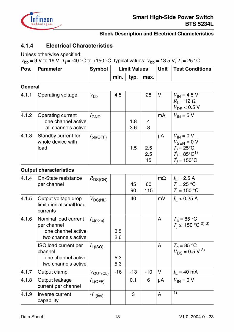
4.1.4 Electrical Characteristics
Unless otherwise specified:Vbb = 9 V to 16 V, Tj = -40 °C to +150 °C, typical values: Vbb = 13.5 V, Tj = 25 °C
Pos. Parameter Symbol Limit Values Unit Test Conditions
min. typ. max.
General
4.1.1 Operating voltage Vbb 4.5 28 V VIN = 4.5 VRL = 12 ΩVDS < 0.5 V
4.1.2 Operating currentone channel activeall channels active
IGND1.83.6
48
mA VIN = 5 V
4.1.3 Standby current for whole device with load
Ibb(OFF)
1.5 2.5 2.5 15
µA VIN = 0 VVSEN = 0 VTj = 25°CTj = 85°C1)
Tj = 150°C
Output characteristics
4.1.4 On-State resistance per channel
RDS(ON)4590
60115
mΩ IL = 2.5 A Tj = 25 °C Tj = 150 °C
4.1.5 Output voltage drop limitation at small load currents
VDS(NL) 40 mV IL < 0.25 A
4.1.6 Nominal load current per channel
one channel activetwo channels active
IL(nom)
3.5 2.6
A Ta = 85 °CTj ≤ 150 °C 2) 3)
ISO load current per channel
one channel activetwo channels active
IL(ISO)
5.35.3
A Tc = 85 °C VDS = 0.5 V 3)
4.1.7 Output clamp VOUT(CL) -16 -13 -10 V IL = 40 mA
4.1.8 Output leakage current per channel
IL(OFF) 0.1 6 µA VIN = 0 V
4.1.9 Inverse current capability
-IL(inv) 3 A 1)
Data Sheet 13 V1.0, 2004-01-23

Smart High-Side Power SwitchBTS 5234L
Block Description and Electrical Characteristics
Note: Characteristics show the deviation of parameter at the given supply voltage andjunction temperature. Typical values show the typical parameters expected frommanufacturing.
Thermal Resistance
4.1.10 Junction to case Rthjc - 2.2 K/W - 1)
4.1.11 Junction to ambient one channel activeall channels active
Rthja--
45 40
K/W - 1)2)
Input characteristics
4.1.12 Input resistor RIN 1.8 3.5 5.5 kΩ4.1.13 L-input level VIN(L) -0.3 1.0 V
4.1.14 H-input level VIN(H) 2.5 5.7 V
4.1.15 L-input current IIN(L) 3 18 75 µA VIN = 0.4 V
4.1.16 H-input current IIN(H) 10 38 75 µA VIN = 5 V
Timings
4.1.17 Turn-on time to 90% Vbb
tON 100 250 µs RL = 12 ΩVbb = 13.5 V
4.1.18 Turn-off time to 10% Vbb
tOFF 120 250 µs RL = 12 ΩVbb = 13.5 V
4.1.19 slew rate 30% to 70% Vbb
dV/ dtON 0.1 0.25 0.5 V/µs RL = 12 ΩVbb = 13.5 V
4.1.20 slew rate 70% to 30% Vbb
-dV/ dtOFF
0.1 0.25 0.5 V/µs RL = 12 ΩVbb = 13.5 V
1) Not subject to production test, specified by design
2) Device mounted on PCB (50 mm x 50 mm x 1.5mm epoxy, FR4) with 6 cm2 copper heatsinking area (onelayer, 70 µm thick) for Vbb connection. PCB is vertical without blown air.
3) Not subject to production test, parameters are calculated from RDS(ON) and Rth
Unless otherwise specified:Vbb = 9 V to 16 V, Tj = -40 °C to +150 °C, typical values: Vbb = 13.5 V, Tj = 25 °C
Pos. Parameter Symbol Limit Values Unit Test Conditions
min. typ. max.
Data Sheet 14 V1.0, 2004-01-23

Smart High-Side Power SwitchBTS 5234L
4.2 Protection Functions
The device provides embedded protective functions. Integrated protection functions aredesigned to prevent IC destruction under fault conditions described in the data sheet.Fault conditions are considered as “outside” normal operating range. Protectionfunctions are neither designed for continuous nor repetitive operation.
4.2.1 Over Load Protection
The load current IOUT is limited by the device itself in case of over load or short circuit toground. There are three steps of current limitation which are selected automaticallydepending on the voltage VDS across the power DMOS. Please note that the voltage atthe OUT pin is Vbb - VDS. Please refer to following figure for details.
Figure 10 Current Limitation (minimum values)
Current limitation is realized by increasing the resistance of the device which leads torapid temperature rise inside. A temperature sensor for each channel causes anoverheated channel to switch off to prevent destruction. After cooling down with thermalhysteresis, the channel switches on again. Please refer to Figure 11 for details.
Figure 11 Shut Down by Over Temperature with Current Limitation
In short circuit condition, the load current is initially limited to IL(LIM). After thermal restart,the current limitation level is reduced to IL(SCr). The current limitation level is reset toIL(LIM) by switching off the device (VIN = 0 V).
IL
CurrentLimitation.emfVDS5 10 15 20
5
10
15
20
25
IN
IL
IIS
t
IL(LIM)
IL(SCr)
t
t
OverLoad.emf
tOFF(SC)
Data Sheet 15 V1.0, 2004-01-23

Smart High-Side Power SwitchBTS 5234L
4.2.2 Reverse Polarity Protection
In case of reverse polarity, the intrinsic body diode causes power dissipation. Additionalpower is dissipated by the integrated ground resistor. Use following formula forestimation of total power dissipation Pdiss(rev) in reverse polarity mode.
The reverse current through the intrinsic body diode has to be limited by the connectedload. The current through sense pins IS1 and IS2 has to be limited (please refer tomaximum ratings on Page 8). The current through the ground pin (GND) is limitedinternally by RGND. The over-temperature protection is not active during reverse polarity.
4.2.3 Over Voltage Protection
In addition to the output clamp for inductive loads as described in Section 4.1.3, there isa clamp mechanism for over voltage protection. Because of the integrated groundresistor, over voltage protection does not require external components.
As shown in Figure 12, in case of supply voltages greater than Vbb(AZ), the powertransistor switches on and the voltage across logic part is clamped. As a result, theinternal ground potential rises to Vbb - Vbb(AZ). Due to the ESD zener diodes, thepotential at pin IN1, IN2 and SEN rises almost to that potential, depending on theimpedance of the connected circuitry.
Figure 12 Over Voltage Protection
4.2.4 Loss of Ground Protection
In case of complete loss of the device ground connections, but connected load ground,the BTS 5234L securely changes to or keeps in off state.
Pdiss(rev) VDS(rev) IL⋅( )all channels∑
Vbb2
RGND
---------------+=
OUT
VBB
OverVoltage.emf
VOUTRGND
logic
GND
IN
IS
SEN RSEN
RIN
ZDESD
ZDAZ
internal ground
Data Sheet 16 V1.0, 2004-01-23

Smart High-Side Power SwitchBTS 5234L
4.2.5 Electrical Characteristics
Unless otherwise specified:Vbb = 9 V to 16 V, Tj = -40 °C to +150 °C , typical values: Vbb = 13.5 V, Tj = 25 °C
Pos. Parameter Symbol Limit Values Unit Test Conditions
min. typ. max.
Over Load Protection
4.2.1 Load current limitation IL(LIM) 23 42 A VDS = 7 V
14 28 A VDS = 14 V
4.2.2 Repetitive short circuit current limitation
IL(SCr) 6 A Tj = Tj(SC) 1)
1) Not subject to production test, specified by design
4.2.3 Initial short circuit shut down time
tOFF(SC) 0.84 ms TjStart = 25 °C 1)
4.2.4 Thermal shut down temperature
Tj(SC) 150 1701)
°C -
4.2.5 Thermal hysteresis ∆Tj 7 K -1)
Reverse Battery
4.2.6 Drain-Source diode voltage (VOUT > Vbb)
-VDS(rev) 900 mV IL = -3.5 AVbb = -13.5 VTj = 150°C
4.2.7 Reverse current through GND pin
-IGND 65 mA Vbb = -13.5 V 1)
Ground Circuit
4.2.8 Integrated Resistor in GND line
RGND 115 220 350 Ω
Over Voltage
4.2.9 Over voltage protection
Vbb(AZ) 41 47 53 V Ibb = 2 mA
Loss of GND
4.2.10 Output leakage current while GND disconnected
IL(GND) 1 mA IIN = 0, ISEN = 0, IIS = 0, IGND = 0 1) 2)
2) no connection at these pins
Data Sheet 17 V1.0, 2004-01-23

Smart High-Side Power SwitchBTS 5234L
4.3 Diagnosis
For diagnosis purpose, the BTS 5234L provides an Enhanced IntelliSense signal at pinsIS1 and IS2. This means in detail, the current sense signal IIS, a proportional signal tothe load current (ratio kILIS = IL / IIS), is provided in ON-state as long as no failure modeoccurs. In case of open load in OFF-state, the voltage VIS(fault) is fed to the diagnosis pin.
Figure 13 Block Diagram: Diagnosis
Table 1 Truth Table
Operation Mode Input Level
Output Level
Diagnostic Output
SEN = H SEN = L
Normal Operation (OFF) L Z Z Z
Short Circuit to GND Z Z Z
Over Temperature Z Z Z
Short Circuit to Vbb Vbb VIS = VIS(fault) Z
Open Load < VOUT(OL) > VOUT(OL)
Z VIS = VIS(fault)
ZZ
channel 1
channel 2
gate control
IIS2
OUT2
IIS1
OUT1
SEN
IS1
µC
IN1
VOUT(OL)
010
101 VIS(fault)
RIN1
RSEN
gate control
IN2
IS2 01
RIN2
diagnosis
GND
ROL
SOL
load
VBB
Sense.emf
RIS1 RIS2
Rlim
Rlim
Data Sheet 18 V1.0, 2004-01-23

Smart High-Side Power SwitchBTS 5234L
4.3.1 ON-State Diagnosis
The standard diagnosis signal is a current sense signal proportional to the load current.The accuracy of the ratio (kILIS = IL / IIS) depends on the temperature. Please refer tofollowing Figure 14 for details. Usually a resistor RIS is connected to the current sensepin. It is recommended to use sense resistors RIS > 500 Ω. A typical value is 4.7 kΩ.
Figure 14 Current sense ratio kILIS1)
Normal Operation (ON) H ~Vbb IIS = IL / kILIS Z
Current Limitation < Vbb Z Z
Short Circuit to GND << Vbb Z Z
Over Temperature Z Z Z
Short Circuit to Vbb Vbb IIS < IL / kILIS Z
Open Load ~Vbb Z Z
L = Low Level, H = High Level, Z = high impedance, potential depends on leakage currents and external circuit
1) The curves show the behavior based on characterization data. The marked points are guaranteed in this DataSheet in Section 4.3.4 (Position 4.3.6).
Table 1 Truth Table
Operation Mode Input Level
Output Level
Diagnostic Output
SEN = H SEN = L
1000
2000
3000
4000
5000
6000
7000
8000
0 0.5 1 1.5 2 2.5 3 3.5 4
k ILI
S
IL /A
dummyTj = 150°C
dummyTj = -40°C
Data Sheet 19 V1.0, 2004-01-23

Smart High-Side Power SwitchBTS 5234L
In case of over current as well as over temperature, the current sense signal is switchedoff. As a result, one threshold is enough to distinguish between normal and faultyoperation. Open load and over load can be differentiated by switching off the channeland using open load detection in off-state.
Details about timings between the diagnosis signal IIS and the output voltage VOUT andload current IL in ON-state can be found in Figure 15.
Figure 15 Timing of Diagnosis Signal in ON-state
4.3.2 OFF-State Diagnosis
Details about timings between the diagnosis signal IIS and the output voltage VOUT andload current IL in OFF-state can be found in Figure 16.
Figure 16 Timing of Diagnosis Signal in OFF-state
SwitchOn.emf
IN
VOUT
IIS
t
t
t
ILt
ON
tON
tsIS(ON) tsIS(LC)
OFF
SwitchOff.emf
IN
VOUT
IIS
t
t
t
ILt
tOFF
Open Load
VIS(fault) / RS
ON OFF
td(fault) ts(fault)
Data Sheet 20 V1.0, 2004-01-23

Smart High-Side Power SwitchBTS 5234L
For open load diagnosis in off state an external output pull-up resistor (ROL) isrecommended. For calculation of the pull-up resistor, just the external leakage currentIleakage and the open load threshold voltage VOUT(OL) has to be taken into account.
Ileakage defines the leakage current in the complete system e.g. caused by humidity.There is no internal leakage current from out to ground at BTS 5234L. Vbb(min) is theminimum supply voltage at which the open load diagnosis in off state must be ensured.
To reduce the stand-by current of the system, an open load resistor switch (SOL) isrecommended.
4.3.3 Sense Enable Function
The diagnosis signals have to be switched on by a high signal at sense enable pin (SEN).See Figure 17 for details on the timing between SEN pin and diagnosis signal IIS.Please note that the diagnosis is disabled, when no signal is provided at pin SEN.
Figure 17 Timing of Sense Enable Signal
The SEN pin circuit is designed equal to the input pin. Please refer to Figure 5 for details.The resistors Rlim are recommended to limit the current through the sense pins IS1 andIS2 in case of reverse polarity and over voltage. Please refer to maximum ratings onPage 8.
The stand-by current of the BTS 5234L is minimized, when both input pins (IN1 and IN2)and the sense enable pin (SEN) are on low level.
ROLVbb(min) VOUT(OL,max)–
Ileakage-----------------------------------------------------------=
tdIS(SEN)tsIS(SEN)t
SEN.emf
tsIS(SEN)
t
tdIS(SEN)IIS
SEN
Data Sheet 21 V1.0, 2004-01-23

Smart High-Side Power SwitchBTS 5234L
4.3.4 Electrical Characteristics
Unless otherwise specified:Vbb = 9 V to 16 V, Tj = -40 °C to +150 °C, VSEN = 5 V, typical values: Vbb = 13.5 V, Tj = 25 °C
Pos. Parameter Symbol Limit Values Unit Test Conditions
min. typ. max.
Open Load at OFF-State
4.3.1 Open load detection threshold voltage
VOUT(OL) 1.6 2.8 4.4 V
4.3.2 Sense signal in case of open load
VIS(fault) 3.5 6.5 V VIN = 0 VVOUT = VbbIIS = 1 mA
4.3.3 Sense signal current limitation
IIS(LIM) 2 mA VIN = 0 VVOUT = Vbb
4.3.4 Sense signal invalid after negative input slope
td(fault) 1.2 ms VIN = 5 V to 0 VVOUT = Vbb
4.3.5 Fault signal settling time
ts(fault) 200 µs VIN = 0 VVOUT = 0 V to
> VOUT(OL)IIS = 1 mA
Load Current Sense ON-State
4.3.6 Current sense ratio kILIS VIN = 5 V
IL = 40 mAIL = 1.3 AIL = 2.2 AIL = 4.0 A
1000230024102465
4035305029202850
8000358033803275
Tj = -40 °C
IL = 40 mAIL = 1.3 AIL = 2.2 AIL = 4.0 A
1400246525202580
3410292028752870
6000327532203160
Tj = 150 °C
4.3.7 Current sense voltage limitation
VIS(LIM) 5.0 6.2 7.5 V IIS = 0.5 mAIL = 3.5 A
4.3.8 Current sense leakage/offset current
IIS(LH) 5 µA VIN = 5 VIL = 0 A
Data Sheet 22 V1.0, 2004-01-23
Smart High-Side Power SwitchBTS 5234L
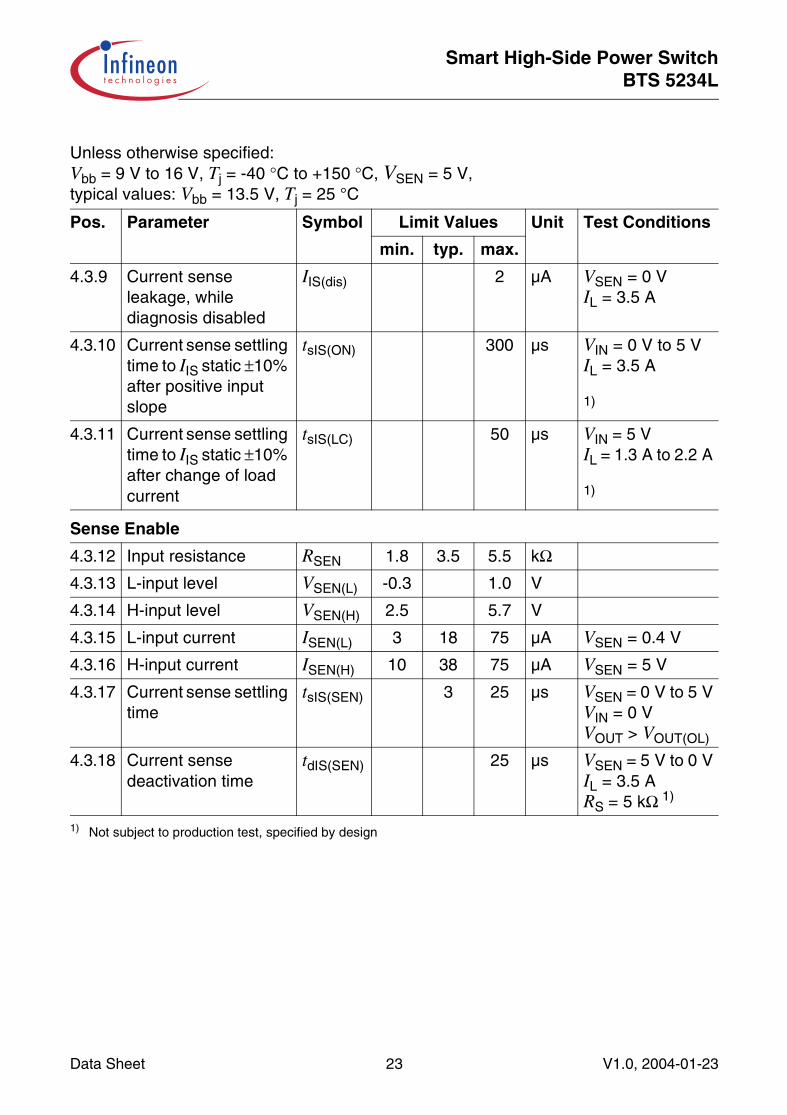
4.3.9 Current sense leakage, while diagnosis disabled
IIS(dis) 2 µA VSEN = 0 VIL = 3.5 A
4.3.10 Current sense settling time to IIS static ±10% after positive input slope
tsIS(ON) 300 µs VIN = 0 V to 5 VIL = 3.5 A
1)
4.3.11 Current sense settling time to IIS static ±10% after change of load current
tsIS(LC) 50 µs VIN = 5 VIL = 1.3 A to 2.2 A
1)
Sense Enable
4.3.12 Input resistance RSEN 1.8 3.5 5.5 kΩ4.3.13 L-input level VSEN(L) -0.3 1.0 V
4.3.14 H-input level VSEN(H) 2.5 5.7 V
4.3.15 L-input current ISEN(L) 3 18 75 µA VSEN = 0.4 V
4.3.16 H-input current ISEN(H) 10 38 75 µA VSEN = 5 V
4.3.17 Current sense settling time
tsIS(SEN) 3 25 µs VSEN = 0 V to 5 VVIN = 0 VVOUT > VOUT(OL)
4.3.18 Current sense deactivation time
tdIS(SEN) 25 µs VSEN = 5 V to 0 VIL = 3.5 ARS = 5 kΩ 1)
1) Not subject to production test, specified by design
Unless otherwise specified:Vbb = 9 V to 16 V, Tj = -40 °C to +150 °C, VSEN = 5 V, typical values: Vbb = 13.5 V, Tj = 25 °C
Pos. Parameter Symbol Limit Values Unit Test Conditions
min. typ. max.
Data Sheet 23 V1.0, 2004-01-23
Smart High-Side Power SwitchBTS 5234L
Package Outlines BTS 5234L
Data Sheet 24 V1.0, 2004-01-23
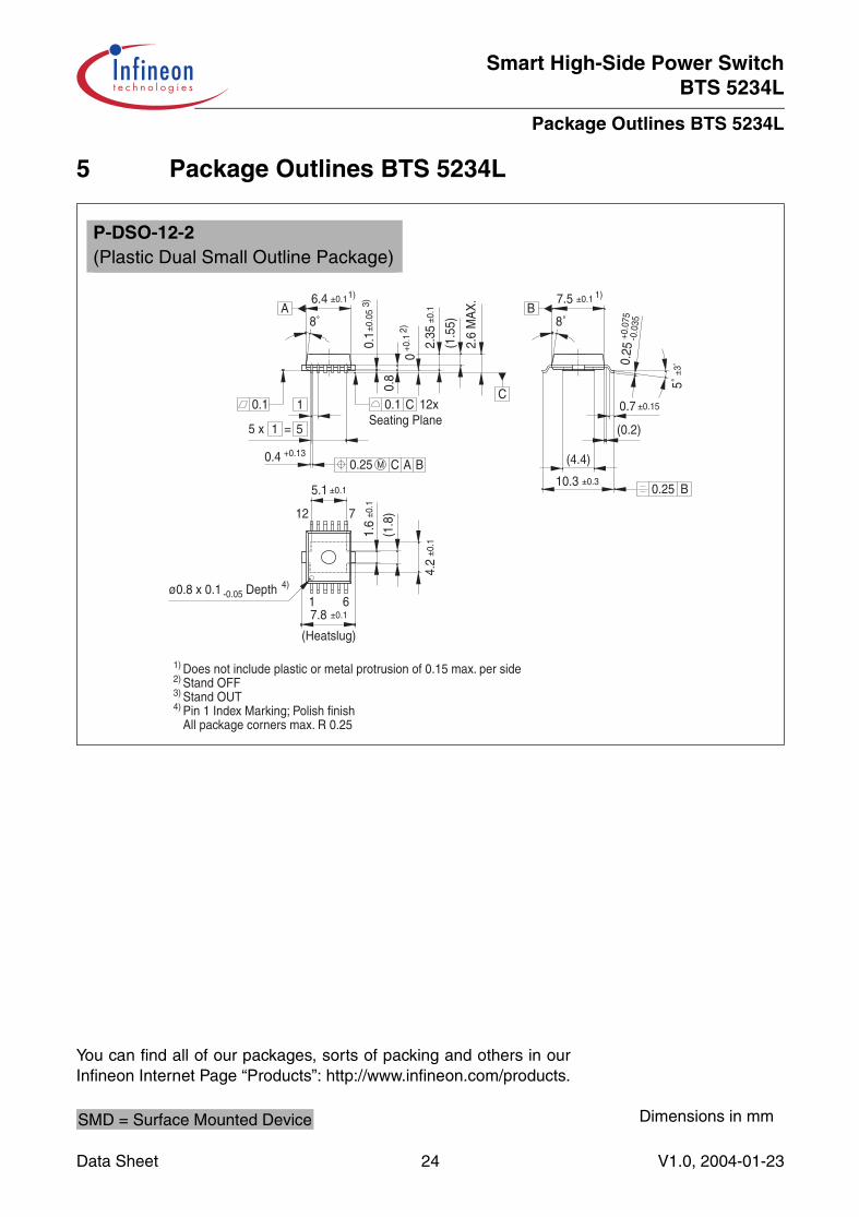
5 Package Outlines BTS 5234L
1 6
712
0.8
(1.5
5)
2.35
±0.1
0.1±
0.05
3)
2.6
MA
X.
C0.1
±0.310.3
(4.4)
4.2
±0.1
(1.8
)±0.1
1.6
ø0.8 x 0.1 -0.05 Depth 4)
+0.130.4
1
5 x 1 = 5
C0.25 M A B
±0.15.1
6.4A
±0.1 7.5B
±0.1
7.8 ±0.1
(Heatslug)
0.25 B
(0.2)
0.7 ±0.15
+0.0
750.
25-0
.035
5˚±3
˚
8˚ 8˚
0.1 12x
1)
Seating Plane+0
.10
2)
Does not include plastic or metal protrusion of 0.15 max. per sideStand OFF
Pin 1 Index Marking; Polish finishStand OUT
All package corners max. R 0.25
1)
2)
3)
4)
1)
C
P-DSO-12-2(Plastic Dual Small Outline Package)
You can find all of our packages, sorts of packing and others in ourInfineon Internet Page “Products”: http://www.infineon.com/products.
Dimensions in mmSMD = Surface Mounted Device

Smart High-Side Power SwitchBTS 5234L
Revision History
6 Revision History
Version Date Changes
V1.0 04-01-23 initial version
Data Sheet 25 2004-01-23

Smart High-Side Power SwitchBTS 5234L
Revision History
Data Sheet 26 V1.0, 2004-01-23

Edition 2004-01-23
Published by Infineon Technologies AG,St.-Martin-Strasse 53,D-81541 München, Germany
© Infineon Technologies AG 1/31/04.All Rights Reserved.
Attention please!
The information herein is given to describe certain components and shall not be considered as warranted characteristics.Terms of delivery and rights to technical change reserved.We hereby disclaim any and all warranties, including but not limited to warranties of non-infringement, regarding circuits, descriptions and charts stated herein.Infineon Technologies is an approved CECC manufacturer.
Information
For further information on technology, delivery terms and conditions and prices please contact your nearest Infineon Technologies Office in Germany or our Infineon Technologies Representatives worldwide.
Warnings
Due to technical requirements components may contain dangerous substances. For information on the types in question please contact your nearest Infineon Technologies Office.Infineon Technologies Components may only be used in life-support devices or systems with the express written approval of Infineon Technologies, if a failure of such components can reasonably be expected to cause the failure of that life-support device or system, or to affect the safety or effectiveness of that device or system. Life support devices or systems are intended to be implanted in the human body, or to support and/or maintain and sustain and/or protect human life. If they fail, it is reasonable to assume that the health of the user or other persons may be endangered.
Smart High-Side Power SwitchBTS 5234L
Data Sheet 27 2004-01-23

h t t p : / / w w w . i n f i n e o n . c o m
Published by Infineon Technologies AG