Broadband powerline communication SoC optimized for · PDF fileBroadband powerline...
38
This is information on a product in full production. February 2018 DocID025777 Rev 2 1/38 ST2100 Broadband powerline communication SoC optimized for audio/video streaming and consumer applications Datasheet - production data Features Configurable HW engine for multiple HomePlug ® PHY and real-time MAC layers processing supporting: – HomePlug AV and 1.0 standards – HomePlug Green PHY™ standard Integrated analog front-end ARM926EJ-S™ 32-bit RISC CPU up to 333 MHz 8/16 bit DDR mobile at 166 MHz and DDR2 at 333 MHz memory controller Serial memory interface 8/16-bits NOR Flash/NAND Flash and SRAM memories controllers Multichannel DMA controller Ethernet 10/100 MAC with MII interface USB 2.0 PCI Express and S-ATA Color LCD (CLCD) controller JPEG codec accelerator Cryptographic coprocessor Up to 40 GPIOs Enhanced I 2 S (digital audio interface) I 2 C master/slave mode Master/slave SSI Two independent UARTs Fast IrDA ® Real-time clock Configurable serial port (SPORT) interface for external DSP and audio codec (ADC and DAC) in I 2 S mode Transport stream interface (video TS) Vectored interrupt controller (VIC) JTAG (IEEE1149.1) interface Three CPU instruction sets Applications The STreamPlug ST2100 is configurable for a wide range of consumer and industrial (a) powerline applications such as: Smart gateway Powerline communication bridging, including wireless Smart grid Electric vehicle charging station (a) In house audio/video distribution Video surveillance Home automation “Network Area Storage” (NAS) Display panels control TFBGA 12 x 12 x 1.2 mm a. Not intended for automotive usage . Table 1. Device summary Order code Operating temp. range Package Packing ST2100 -40 to +85 °C TFBGA 12 x 12 x 1.2 mm, pitch 0.5 mm Tray, tape and reel www.st.com
Transcript of Broadband powerline communication SoC optimized for · PDF fileBroadband powerline...
This is information on a product in full production.
February 2018 DocID025777 Rev 2 1/38
ST2100
Broadband powerline communication SoC optimized foraudio/video streaming and consumer applications
Datasheet - production data
Features
Configurable HW engine for multiple HomePlug® PHY and real-time MAC layers processing supporting:
– HomePlug AV and 1.0 standards
– HomePlug Green PHY™ standard
Integrated analog front-end
ARM926EJ-S™ 32-bit RISC CPU up to 333 MHz
8/16 bit DDR mobile at 166 MHz and DDR2 at 333 MHz memory controller
Serial memory interface
8/16-bits NOR Flash/NAND Flash and SRAM memories controllers
Multichannel DMA controller
Ethernet 10/100 MAC with MII interface
USB 2.0
PCI Express and S-ATA
Color LCD (CLCD) controller
JPEG codec accelerator
Cryptographic coprocessor
Up to 40 GPIOs
Enhanced I2S (digital audio interface)
I2C master/slave mode
Master/slave SSI
Two independent UARTs
Fast IrDA®
Real-time clock
Configurable serial port (SPORT) interface for external DSP and audio codec (ADC and DAC) in I2S mode
Transport stream interface (video TS)
Vectored interrupt controller (VIC)
JTAG (IEEE1149.1) interface
Three CPU instruction sets
Applications
The STreamPlug ST2100 is configurable for a wide range of consumer and industrial(a) powerline applications such as:
Smart gateway
Powerline communication bridging, including wireless
Smart grid
Electric vehicle charging station(a)
In house audio/video distribution
Video surveillance
Home automation
“Network Area Storage” (NAS)
Display panels control
TFBGA 12 x 12 x 1.2 mm
a. Not intended for automotive usage .
Table 1. Device summary
Order code
Operating temp. range
Package Packing
ST2100 -40 to +85 °CTFBGA 12 x 12 x
1.2 mm, pitch 0.5 mm
Tray, tape and reel
www.st.com
Contents ST2100
2/38 DocID025777 Rev 2
Contents
1 Description . . . . . . . . . . . . . . . . . . . . . . . . . . . . . . . . . . . . . . . . . . . . . . . . . 6
2 Main features . . . . . . . . . . . . . . . . . . . . . . . . . . . . . . . . . . . . . . . . . . . . . . . 7
3 Architecture description . . . . . . . . . . . . . . . . . . . . . . . . . . . . . . . . . . . . . . 9
3.1 CPU subsystem . . . . . . . . . . . . . . . . . . . . . . . . . . . . . . . . . . . . . . . . . . . . 10
3.2 System bus . . . . . . . . . . . . . . . . . . . . . . . . . . . . . . . . . . . . . . . . . . . . . . . . 10
3.3 Memory subsystem . . . . . . . . . . . . . . . . . . . . . . . . . . . . . . . . . . . . . . . . . .11
3.4 Expi subsystem . . . . . . . . . . . . . . . . . . . . . . . . . . . . . . . . . . . . . . . . . . . . .11
3.5 Basic subsystem . . . . . . . . . . . . . . . . . . . . . . . . . . . . . . . . . . . . . . . . . . . .11
3.6 High-speed connectivity subsystem . . . . . . . . . . . . . . . . . . . . . . . . . . . . . 12
3.7 Low-speed connectivity subsystem . . . . . . . . . . . . . . . . . . . . . . . . . . . . . 12
3.8 Application subsystem . . . . . . . . . . . . . . . . . . . . . . . . . . . . . . . . . . . . . . . 13
3.9 Clock and reset system . . . . . . . . . . . . . . . . . . . . . . . . . . . . . . . . . . . . . . 13
4 Pin descriptions . . . . . . . . . . . . . . . . . . . . . . . . . . . . . . . . . . . . . . . . . . . 14
4.1 Dedicated pins . . . . . . . . . . . . . . . . . . . . . . . . . . . . . . . . . . . . . . . . . . . . . 14
4.2 Shared I/O pins (MFIOs) . . . . . . . . . . . . . . . . . . . . . . . . . . . . . . . . . . . . . 22
4.3 Required external components . . . . . . . . . . . . . . . . . . . . . . . . . . . . . . . . 27
5 Memory map . . . . . . . . . . . . . . . . . . . . . . . . . . . . . . . . . . . . . . . . . . . . . . 28
6 Clocking parameters . . . . . . . . . . . . . . . . . . . . . . . . . . . . . . . . . . . . . . . . 30
6.1 Master clock (MCLK) . . . . . . . . . . . . . . . . . . . . . . . . . . . . . . . . . . . . . . . . 30
6.2 Real-time clock (RTC) . . . . . . . . . . . . . . . . . . . . . . . . . . . . . . . . . . . . . . . 31
6.3 PCIe/SATA clock . . . . . . . . . . . . . . . . . . . . . . . . . . . . . . . . . . . . . . . . . . . 31
7 Electrical characteristics . . . . . . . . . . . . . . . . . . . . . . . . . . . . . . . . . . . . 32
7.1 Absolute maximum ratings . . . . . . . . . . . . . . . . . . . . . . . . . . . . . . . . . . . . 32
7.2 Power consumption . . . . . . . . . . . . . . . . . . . . . . . . . . . . . . . . . . . . . . . . . 32
7.3 DC electrical characteristics . . . . . . . . . . . . . . . . . . . . . . . . . . . . . . . . . . . 33
7.4 Power-up and reset sequence . . . . . . . . . . . . . . . . . . . . . . . . . . . . . . . . . 34
7.5 Internal 2.5 V linear regulator . . . . . . . . . . . . . . . . . . . . . . . . . . . . . . . . . . 34
DocID025777 Rev 2 3/38
ST2100 Contents
38
8 Package information . . . . . . . . . . . . . . . . . . . . . . . . . . . . . . . . . . . . . . . . 35
8.1 TFBGA 12 x 12 x 1.2 mm package information . . . . . . . . . . . . . . . . . . . . 35
9 Revision history . . . . . . . . . . . . . . . . . . . . . . . . . . . . . . . . . . . . . . . . . . . 37
List of tables ST2100
4/38 DocID025777 Rev 2
List of tables
Table 1. Device summary . . . . . . . . . . . . . . . . . . . . . . . . . . . . . . . . . . . . . . . . . . . . . . . . . . . . . . . . . . 1Table 2. System bus connectivity . . . . . . . . . . . . . . . . . . . . . . . . . . . . . . . . . . . . . . . . . . . . . . . . . . . 10Table 3. Key to system bus connectivity matrix . . . . . . . . . . . . . . . . . . . . . . . . . . . . . . . . . . . . . . . . 10Table 4. Master clock RTC, RESET and 3.3 V comparator pin descriptions . . . . . . . . . . . . . . . . . . 14Table 5. Power supply pin descriptions . . . . . . . . . . . . . . . . . . . . . . . . . . . . . . . . . . . . . . . . . . . . . . 14Table 6. Debug pin descriptions . . . . . . . . . . . . . . . . . . . . . . . . . . . . . . . . . . . . . . . . . . . . . . . . . . . . 17Table 7. Boot source descriptions . . . . . . . . . . . . . . . . . . . . . . . . . . . . . . . . . . . . . . . . . . . . . . . . . . 17Table 8. Boot source selection . . . . . . . . . . . . . . . . . . . . . . . . . . . . . . . . . . . . . . . . . . . . . . . . . . . . . 18Table 9. SMI pin descriptions . . . . . . . . . . . . . . . . . . . . . . . . . . . . . . . . . . . . . . . . . . . . . . . . . . . . . . 18Table 10. USB Pin descriptions . . . . . . . . . . . . . . . . . . . . . . . . . . . . . . . . . . . . . . . . . . . . . . . . . . . . . 18Table 11. PCIe / SATA pin descriptions . . . . . . . . . . . . . . . . . . . . . . . . . . . . . . . . . . . . . . . . . . . . . . . 19Table 12. Internal AFE pin descriptions . . . . . . . . . . . . . . . . . . . . . . . . . . . . . . . . . . . . . . . . . . . . . . . 19Table 13. AC crossing pin descriptions . . . . . . . . . . . . . . . . . . . . . . . . . . . . . . . . . . . . . . . . . . . . . . . 19Table 14. External PLI pin description . . . . . . . . . . . . . . . . . . . . . . . . . . . . . . . . . . . . . . . . . . . . . . . . 19Table 15. DDR pin descriptions . . . . . . . . . . . . . . . . . . . . . . . . . . . . . . . . . . . . . . . . . . . . . . . . . . . . . 20Table 16. MFIO pin descriptions. . . . . . . . . . . . . . . . . . . . . . . . . . . . . . . . . . . . . . . . . . . . . . . . . . . . . 23Table 17. Memory map description . . . . . . . . . . . . . . . . . . . . . . . . . . . . . . . . . . . . . . . . . . . . . . . . . . 28Table 18. EXPI clock characteristics . . . . . . . . . . . . . . . . . . . . . . . . . . . . . . . . . . . . . . . . . . . . . . . . . 31Table 19. Absolute maximum rating . . . . . . . . . . . . . . . . . . . . . . . . . . . . . . . . . . . . . . . . . . . . . . . . . . 32Table 20. Power consumption . . . . . . . . . . . . . . . . . . . . . . . . . . . . . . . . . . . . . . . . . . . . . . . . . . . . . . 32Table 21. Power consumption using 2.5 V internal LDO . . . . . . . . . . . . . . . . . . . . . . . . . . . . . . . . . . 33Table 22. Recommended operating conditions . . . . . . . . . . . . . . . . . . . . . . . . . . . . . . . . . . . . . . . . . 33Table 23. Thermal recommended ratings. . . . . . . . . . . . . . . . . . . . . . . . . . . . . . . . . . . . . . . . . . . . . . 33Table 24. Internal 2.5 V voltage regulator specifications . . . . . . . . . . . . . . . . . . . . . . . . . . . . . . . . . . 34Table 25. TFBGA 12 x 12 x 1.2 mm, 324 + 49 balls, 4R23 x 23, pitch 0.5 mm,
ball 0.3 mm package mechanical data . . . . . . . . . . . . . . . . . . . . . . . . . . . . . . . . . . . . . . . . 36Table 26. TFGBA package thermal characteristics . . . . . . . . . . . . . . . . . . . . . . . . . . . . . . . . . . . . . . 36Table 27. Document revision history . . . . . . . . . . . . . . . . . . . . . . . . . . . . . . . . . . . . . . . . . . . . . . . . . 37
DocID025777 Rev 2 5/38
ST2100 List of figures
38
List of figures
Figure 1. STreamPlug ST2100 functional block diagram . . . . . . . . . . . . . . . . . . . . . . . . . . . . . . . . . . 9Figure 2. MIFO 0-87 muxing scheme . . . . . . . . . . . . . . . . . . . . . . . . . . . . . . . . . . . . . . . . . . . . . . . . 22Figure 3. MFIO 88-103 muxing scheme . . . . . . . . . . . . . . . . . . . . . . . . . . . . . . . . . . . . . . . . . . . . . . 22Figure 4. MCLK crystal connections . . . . . . . . . . . . . . . . . . . . . . . . . . . . . . . . . . . . . . . . . . . . . . . . . 30Figure 5. RTC crystal connection. . . . . . . . . . . . . . . . . . . . . . . . . . . . . . . . . . . . . . . . . . . . . . . . . . . . 31Figure 6. Power-up and reset sequence . . . . . . . . . . . . . . . . . . . . . . . . . . . . . . . . . . . . . . . . . . . . . . 34Figure 7. TFBGA 12 x 12 x 1.2 mm, 324 + 49 balls, 4R23 x 23, pitch 0.5 mm,
ball 0.3 mm package outline . . . . . . . . . . . . . . . . . . . . . . . . . . . . . . . . . . . . . . . . . . . . . . . 35
Description ST2100
6/38 DocID025777 Rev 2
1 Description
The STreamPlug ST2100 device is the STMicroelectronics® “Broad Band Powerline Communication” (BB PLC) solution, based on the powerful ARM926EJ-S™ processor (up to 333 MHz), widely used in applications where high computation performance is required, such as consumer (“Home Area Network” or HAN), industrial and smart grid applications.
In addition, the STreamPlug ST2100 has a memory management unit (MMU) that allows virtual memory management - making the system compliant with the Linux® operating system. It also offers 16 Kbyte of data cache, 32 Kbyte of instruction cache, JTAG and ETM™ (Embedded Trace Macrocell™ ) for debug operations.
A large set of peripherals allows a wide flexibility of the usage of the system in most of the possible PLC broadband applications (indoor and outdoor).
DocID025777 Rev 2 7/38
ST2100 Main features
38
2 Main features
Configurable hardware engine for multiple HomePlug PHY and real-time MAC layers
– HomePlug™ AV and 1.0 standards
– HomePlug Green PHY standard
Integrated analog front-end
– Programmable gain amplifier: gain range -12 dB to 48 dB
– ADC and DAC
– 2.5 V voltage regulator
– Zero crossing (ZC) comparator
ARM926EJ-S™ 32-bit RISC CPU up to 333 MHz
– 16 Kbyte if instruction cache, 16 Kbyte of data cache
– 32 Kbyte of instruction TCM and 16 Kbyte of data TCM
– Three instruction sets: 32-bit for high performance, 16-bit (Thumb®) for efficient code density, bytecode Java™ mode (Jazelle™) for direct execution of Java code
– AMBA™ bus interface with fMAX 166 MHz
48 Kbyte on-chip boot ROM
8 Kbyte on-chip SRAM
8/16 bit DDR mobile at 166 MHz and DDR2 at 333 MHz memory controller
Serial memory interface
8/16-bits NOR Flash/NAND Flash and SRAM memory controller
Boot capability from NAND Flash, serial/parallel NOR Flash, and UART
Multichannel DMA controller (8 FIFOs and 16 dedicated channels)
Ethernet 10/100 MAC with MII interface (IEEE 802.3), RevMII, IEEE 802.1-AS and 802.1-Qav for audio video (AV) traffic
USB 2.0 (high-full-low speed) port with an integrated PHY able to work as a host or device
PCI Express GEN1 (PCI Express standard version 1.1), single lane X1 dual mode (both “Root Complex” and “Endpoint” modes supported), the PHY is a standard 8-bit/16-bit PIPE PHY interface. This peripheral supports also the serial ATA compliant with the SATA/150.
Color LCD controller (up to 1024 x 768 resolution at 24 bpp true color, STN/TFT display panels)
JPEG codec accelerator (1 clock/pixel)
Cryptographic coprocessor (DMA based programmable engine) with support for:
– Advanced encryption standard (AES) cipher (128, 192, 256 bit keys) in ECB, CBC, CTR modes
– Data encryption standard (DES) and triple DES (TDES) cipher in ECB and CBC modes
– SHA-1, HMAC-SHA-1, SHA-256, HMAC-SHA-256, MD5, HMAC-MD5 digests
Up to 40 GPIOs (multiplexed with peripheral I/Os), all the I/Os have interrupt capability, 24 application specific GPIOs: four I/Os support PWM and four I/Os support double PWM features.
Main features ST2100
8/38 DocID025777 Rev 2
Enhanced I2S for 4-channel “Digital Audio Interface“ (DAI)
Master/slave SSP (Motorola SPI, Texas Instruments, National Semiconductor protocols) up to 5 Mbits/s in slave mode and up to 20 Mbits/s in master mode
I2C master/slave mode
Two independent UARTs supporting hardware (HW) flow control
Fast IrDA (SIR/MIR/FIR)
Three pairs of 16-bit general purpose timers with programmable 8-bit prescaler
Real-time clock (RTC)
Configurable serial port (SPORT) interface for external DSP and audio codec (ADC and DAC in I2S mode)
Transport stream interface (Video TS also called “Synchronous peripheral bus”) for external MPEG- 2/H.264 encoder and decoder. TS port also implements image sensor interface (CCD camera)
Watchdog timer
Clock synthesizer (4 outputs)
Vectored interrupt controller (VIC)
JTAG (IEEE1149.1) interface
ETM9 interface
Multichannel cryptographic coprocessor. DES/TDES and AES security for the powerline link
PGC (IR) interface
Supply voltages: 1.2 V core, 1.8 V / 2.5 V DDR, 2.5 V AFE and PLLs, 1.5 V RTC and 3.3 V I/Os
Available in a TFBGA373 package (12 x 12 x 1.2 mm, pitch 0.5 mm).
DocID025777 Rev 2 9/38
ST2100 Architecture description
38
3 Architecture description
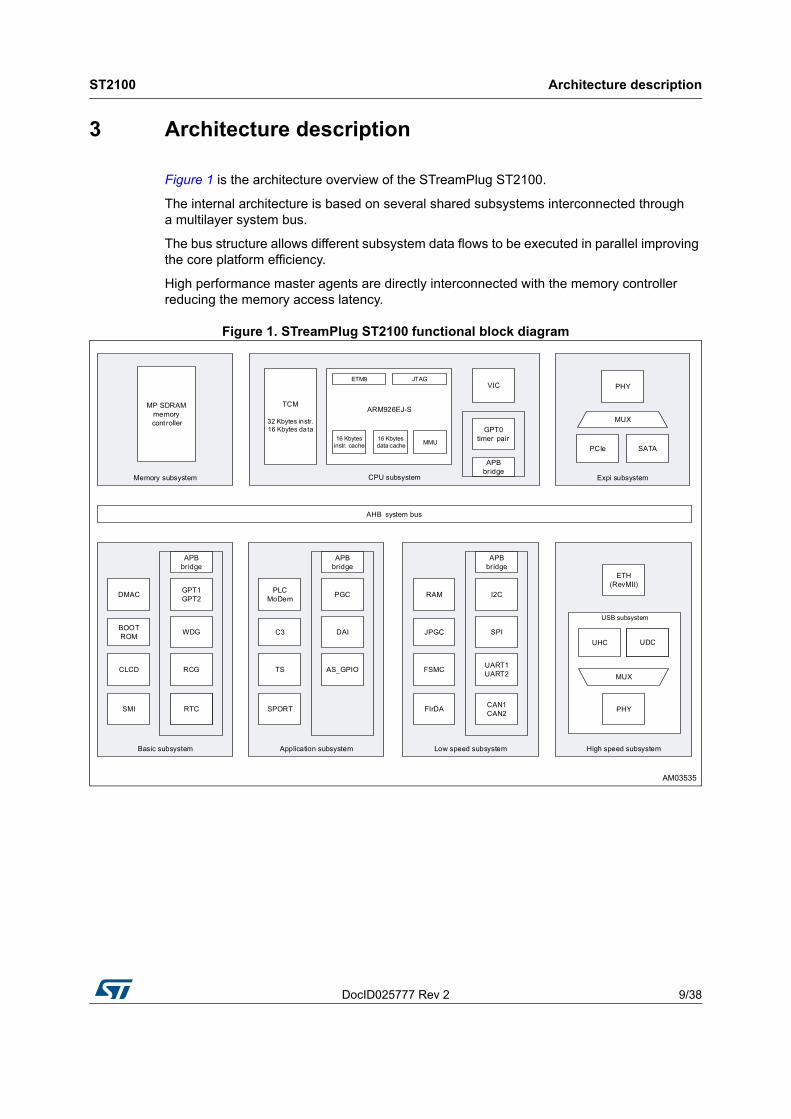
Figure 1 is the architecture overview of the STreamPlug ST2100.
The internal architecture is based on several shared subsystems interconnected through a multilayer system bus.
The bus structure allows different subsystem data flows to be executed in parallel improving the core platform efficiency.
High performance master agents are directly interconnected with the memory controller reducing the memory access latency.
Figure 1. STreamPlug ST2100 functional block diagram
Architecture description ST2100
10/38 DocID025777 Rev 2
3.1 CPU subsystem
ARM926EJ-S™ running at 333 MHz with:
– MMU
– 16 Kbyte of instruction cache
– 16 Kbyte of data cache
– 32 Kbyte of instruction “Tightly Coupled Memory“ (TCM)
– 16 Kbyte of data “Tightly Coupled Memory” (TCM)
– AMBA bus interface
– JTAG
– ETM9 (Embedded Trace Macrocell) for debug, medium size version
Interrupt controller managing sources which are prioritized and vectorized
3.2 System bus
The system bus structure allows different subsystem data flows to be executed in parallel improving the core platform efficiency.
High performance master agents are directly interconnected with the memory controller reducing the memory access latency. The overall memory bandwidth assigned to each master port can be programmed and optimized through an internal efficient weighted round-robin arbitration mechanism.
Table 2 shows the system bus scheme and Table 3 is the key to its contents.
Table 2. System bus connectivity
CP
U
PC
Ie/S
ATA
DM
A 1
DM
A 2
Eth
.
TS
/SP
OR
T
UH
C/U
DC
PL
C m
od
em
Cry
pto
CL
CD
Targets (slave ports)
MP SDRAM X X X X X X X X X X
Low speed X X X
Application X X X
Basic X X
High speed X X
Expi X X
Table 3. Key to system bus connectivity matrix
Format Definition
Grey box No connection exists between target and initiator
X A connection exists between target and initiator
DocID025777 Rev 2 11/38
ST2100 Architecture description
38
3.3 Memory subsystem
The multiport memory controller within the memory subsystem manages DDR mobile up to 166 MHz and DDR2 up to 333 MHz external memory. Internally, it handles 5 ports supporting all the chip master ports.
The multiport memory controller block has a programmable arbitration scheme and the transactions happen on a different layer from the main bus. It also offers a local FIFO to increase the throughput and reduce the latency.
3.4 Expi subsystem
PCI Express Gen1 (PCI Express standard version 1.1) single lane X1 dual mode
– Root Complex mode is supported.
– Endpoint mode is supported.
Serial ATA compliant with SATA/150 specifications
PHY is standard 8-bit/16-bit PIPE PHY interface
3.5 Basic subsystem
8 FIFOs and 16 high performance DMA channels with two AHB interfaces to parallelize the activity when two channels are working at the same time.
48 Kbytes of ROM (for boot procedure)
“Serial Memory Interface” (SMI) supporting external serial Flash.
Color LCD controller (CLCD) up to 1024 x 768 resolution at 24 bpp (true color) supporting STN/TFT display panels
Three pair of 16 bit general purpose timers with programmable prescaler
Watchdog timer
RTC with separate power supply allowing battery connection
Up to 104 “Multi-Function” I/Os (MFIOs) multiplexed with peripheral I/Os:
– Allows a large number of possible application scenarios
– Up to 40 GPIOs with interrupt capability
System controller, reset and clock generation, and miscellaneous registers array allowing a full configurability of the system.
Architecture description ST2100
12/38 DocID025777 Rev 2
3.6 High-speed connectivity subsystem
Ethernet 10/100 MAC with MII interface (IEEE 802.3), with external PHY
– RevMII (supporting 25 and 50 MHz clock frequencies)
– IEEE 802.1-AS and 802.1-Qav for audio video (AV) traffic
USB 2.0 (high-full-low speed) port with integrated PHY able to work as a host or device. The PHY is embedded.
– One USB host controller compatible with USB 2.0 high-speed specification managing a single port. The peripheral has a dedicated channel to the multiport memory controller and a dedicated slave port for CPU programming (OHCI and EHCI).
– One USB device compatible with USB 2.0 high-speed specifications. A dedicated channel connects the peripheral with the multiport memory controller and registers and an internal FIFO are accessible from the CPU through the main AHB bus. A USB plug detector block is also available to detect the presence of the VBUS voltage.
3.7 Low-speed connectivity subsystem
Two independent UARTs supporting hardware flow control up to 460.8 Kbits/s
Fast IrDA controller with a speed rate from 9.6 Kbits/s to 4 Mbits/s (SIR/MIR/FIR)
One synchronous “Serial Port Interface” (SPI) controller capable of operating as a master or a slave (Motorola - Texas Instruments - National Semiconductor) with a speed (data) rate up to 20 Mbits/s
One I2C (also known as a digital audio interface) controller capable of operating in master and slave mode and covering all the possible data rates (high, fast and low)
JPEG codec accelerator (1 clock per pixel)
8 Kbytes of static RAM
“Flexible Static Memory Controller” (FSMC) supporting:
– Asynchronous parallel NAND and NOR Flash memories
– Synchronous and asynchronous SRAM
Two independent “Controller Area Network” (CAN) interfaces compliant with CAN protocol version 2.0 parts A and B (up to 1 Mbit/s).
DocID025777 Rev 2 13/38
ST2100 Architecture description
38
3.8 Application subsystem
Configurable hardware engine for multiple HomePlug PHY and real-time MAC layers processing supporting:
– HomePlug AV and 1.0 standards
– HomePlug Green PHY standard
Integrated analog front-end:
– Programmable gain amplifier: gain range -12 dB to 48 dB
– ADC and DAC
– 2.5 V, 150 mA voltage regulator
– Zero crossing (ZC) comparator
Cryptographic coprocessor channels (C3), DMA based programmable engine, with support for:
– Advanced encryption standard (AES) cipher (128-, 192-, 256-bit keys) in ECB, CBC, CTR modes
– Data encryption standard (DES) and triple DES cipher in ECB and CBC modes
– SHA-1, HMAC-SHA-1, SHA-256, HMAC-SHA-256, MD5, HMAC-MD5 digests algorithms
Configurable serial port (SPORT) interface for external DSP and audio codec (ADC and DAC in I2S mode)
Transport stream (TS) interface
Pulse generator and capture (PGC) (IR) for remote controls
4-channel I2S [“Digital Audio Interface” (DAI)]
24 application specific GPIOs:
– Up to 4 GPIOs supporting PWM
– Up to 4 GPIOs supporting double PWM.
3.9 Clock and reset system
The system clocks are generated by:
– Two fully programmable PLLs. One is used to generate a clock for CPU and AMBA AHB bus and the other is used in case the DDR clock has to be different (asynchronous) with respect to the CPU clock.
– One “high precision” clock synthesizer with 4 outputs providing different frequencies for the various IPs
Fully programmable control of the clock and reset signals for all the slave blocks allowing sophisticated power management.
Pin descriptions ST2100
14/38 DocID025777 Rev 2
4 Pin descriptions
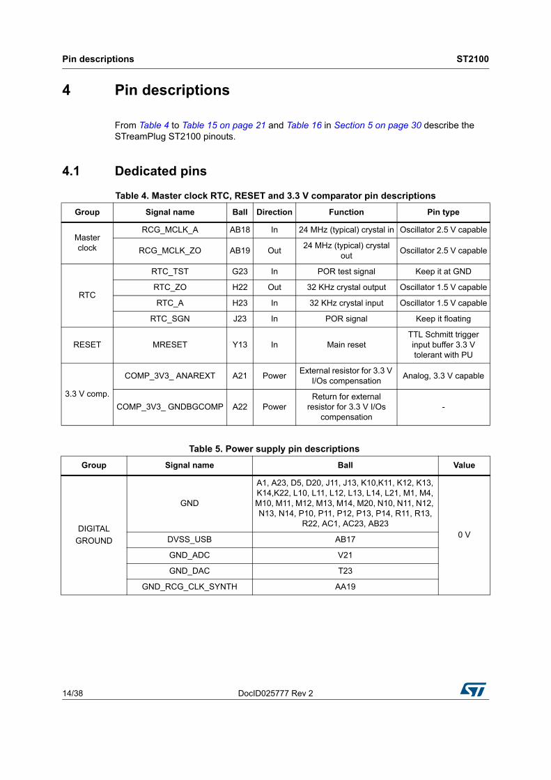
From Table 4 to Table 15 on page 21 and Table 16 in Section 5 on page 30 describe the STreamPlug ST2100 pinouts.
4.1 Dedicated pins
Table 4. Master clock RTC, RESET and 3.3 V comparator pin descriptions
Group Signal name Ball Direction Function Pin type
Master clock
RCG_MCLK_A AB18 In 24 MHz (typical) crystal in Oscillator 2.5 V capable
RCG_MCLK_ZO AB19 Out24 MHz (typical) crystal
outOscillator 2.5 V capable
RTC
RTC_TST G23 In POR test signal Keep it at GND
RTC_ZO H22 Out 32 KHz crystal output Oscillator 1.5 V capable
RTC_A H23 In 32 KHz crystal input Oscillator 1.5 V capable
RTC_SGN J23 In POR signal Keep it floating
RESET MRESET Y13 In Main resetTTL Schmitt trigger input buffer 3.3 V tolerant with PU
3.3 V comp.
COMP_3V3_ ANAREXT A21 PowerExternal resistor for 3.3 V
I/Os compensationAnalog, 3.3 V capable
COMP_3V3_ GNDBGCOMP A22 PowerReturn for external
resistor for 3.3 V I/Os compensation
-
Table 5. Power supply pin descriptions
Group Signal name Ball Value
DIGITAL
GROUND
GND
A1, A23, D5, D20, J11, J13, K10,K11, K12, K13, K14,K22, L10, L11, L12, L13, L14, L21, M1, M4, M10, M11, M12, M13, M14, M20, N10, N11, N12, N13, N14, P10, P11, P12, P13, P14, R11, R13,
R22, AC1, AC23, AB230 V
DVSS_USB AB17
GND_ADC V21
GND_DAC T23
GND_RCG_CLK_SYNTH AA19
DocID025777 Rev 2 15/38
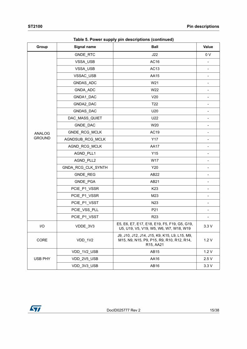
ST2100 Pin descriptions
38
ANALOG GROUND
GNDE_RTC J22 0 V
VSSA_USB AC16 -
VSSA_USB AC13 -
VSSAC_USB AA15 -
GNDAS_ADC W21 -
GNDA_ADC W22 -
GNDA1_DAC V20 -
GNDA2_DAC T22 -
GNDAS_DAC U20 -
DAC_MASS_QUIET U22 -
GNDE_DAC W20 -
GNDE_RCG_MCLK AC19 -
AGNDSUB_RCG_MCLK Y17 -
AGND_RCG_MCLK AA17 -
AGND_PLL1 Y15 -
AGND_PLL2 W17 -
GNDA_RCG_CLK_SYNTH Y20 -
GNDE_REG AB22 -
GNDE_PGA AB21 -
PCIE_P1_VSSR K23 -
PCIE_P1_VSSR M23 -
PCIE_P1_VSST N23 -
PCIE_VSS_PLL P21 -
PCIE_P1_VSST R23 -
I/O VDDE_3V3E5, E6, E7, E17, E18, E19, F5, F19, G5, G19,
U5, U19, V5, V19, W5, W6, W7, W18, W193.3 V
CORE VDD_1V2J9, J10, J12, J14, J15, K9, K15, L9, L15, M9, M15, N9, N15, P9, P15, R9, R10, R12, R14,
R15, AA211.2 V
USB PHY
VDD_1V2_USB AB15 1.2 V
VDD_2V5_USB AA16 2.5 V
VDD_3V3_USB AB16 3.3 V
Table 5. Power supply pin descriptions (continued)
Group Signal name Ball Value
Pin descriptions ST2100
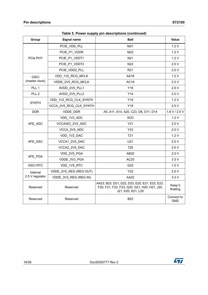
16/38 DocID025777 Rev 2
PCIe PHY
PCIE_VDD_PLL M21 1.2 V
PCIE_P1_VDDR M22 1.2 V
PCIE_P1_VDDT1 N21 1.2 V
PCIE_P1_VDDT2 N22 2.5 V
PCIE_VDD2_PLL R21 2.5 V
OSCI (master clock)
VDD_1V2_RCG_MCLK AA18 1.2 V
VDDE_2V5_RCG_MCLK AC18 2.5 V
PLL 1 AVDD_2V5_PLL1 Y16 2.5 V
PLL 2 AVDD_2V5_PLL2 Y14 2.5 V
SYNTHVDD_1V2_RCG_CLK_SYNTH Y19 1.2 V
VCCA_2V5_RCG_CLK_SYNTH Y18 2.5 V
DDR VDDE_DDR A5, A11, A14, A20, C23, D6, D11, D14 1.8 V / 2.5 V
AFE_ADC
VDD_1V2_ADC W23 1.2 V
VCCAISO_2V5_ADC Y21 2.5 V
VCCA_2V5_ADC Y23 2.5 V
AFE_DAC
VDD_1V2_DAC T21 1.2 V
VCCA1_2V5_DAC U21 2.5 V
VCCA2_2V5_DAC T20 2.5 V
AFE_PGAVDD_2V5_PGA AB20 2.5 V
VDDE_3V3_PGA AC20 3.3 V
OSCI RTC VDD_1V5_RTC G22 1.5 V
Internal 2.5 V regulator
VDDE_2V5_REG (REG OUT) Y22 2.5 V
VDDE_3V3_REG (REG IN) AA22 3.3 V
Reserved ReservedAA23, B23, D21, D22, D23, E20, E21, E22, E23, F20, F21, F22, F23, G20, G21, H20, H21, J20,
J21, K20, K21, L20
Keep it floating
Reserved Reserved B22Connect to
GND
Table 5. Power supply pin descriptions (continued)
Group Signal name Ball Value
DocID025777 Rev 2 17/38
ST2100 Pin descriptions
38
Table 6. Debug pin descriptions
Signal name Ball Direction Function Pin type
Reserved B4 InReserved
Connect to GNDTTL input buffer, 3.3 V
tolerant with PD
JTAG_TMS C5 In Test mode selectTTL input buffer, 3.3 V
tolerant with PU
JTAG_TCK D4 In Test clockTTL input buffer, 3.3 V
tolerant with PU
JTAG_NTRST E4 In Test reset inputTTL input buffer, 3.3 V
tolerant with PU
JTAG_TDI F4 In Test data inputTTL input buffer, 3.3 V
tolerant with PU
JTAG_TDO G4 Out Test data outputTTL output buffer, 3.3 V
capable, 4 mA
ETM_TRACECLK Y7 OutETM clock (the other ETM
signals are available on MFIOs)TTL output buffer, 3.3 V
capable, 4 mA
Table 7. Boot source descriptions
Signal name Ball Direction Function Pin type
SOC_CFG_BOOT0 C2 In Boot mode configurationTTL input buffer, 3.3 V
tolerant with PD
SOC_CFG_BOOT1 B2 In Boot mode configurationTTL input buffer, 3.3 V
tolerant with PD
SOC_CFG_BOOT2 C3 In Boot mode configurationTTL input buffer, 3.3 V
tolerant with PD
SOC_CFG_BOOT3 B3 In Boot mode configurationTTL input buffer, 3.3 V
tolerant with PD
Pin descriptions ST2100
18/38 DocID025777 Rev 2
Table 8. Boot source selection
Boot source SOC_CFG_BOOT3 SOC_CFG_BOOT2 SOC_CFG_BOOT1 SOC_CFG_BOOT0
SMI (3-byte addressing) 0 0 0 0
SMI (2-byte addressing) 0 0 0 1
FSMC/NAND 8-bit 0 0 1 0
FSMC/NAND 16-bit 0 0 1 1
UART1 (G20) 0 1 0 0
UART2(G21) 0 1 0 1
FSMC/NOR 8-bit 0 1 1 0
FSMC/NOR 16-bit 0 1 1 1
Reserved 1 X(1) X(1) X(1)
1. An “X” may be a “1” or a “0”.
Table 9. SMI pin descriptions
Signal name Ball Direction Function Pin type
SMI_DIN A2 In Serial Flash input dataTTL input buffer, 3.3 V tolerant with
configurable PU/PD and HYST
SMI_DOUT A3 Out Serial Flash output data TTL output buffer, 3.3 V capable, 4 mA
SMI_CLK A4 I/O Serial Flash clock TTL output buffer, 3.3 V capable, 4 mA
SMI_NCS0 B1 Out Serial Flash chip select TTL output buffer, 3.3 V capable, 4 mA
SMI_NCS1 C1 Out Serial Flash chip select TTL output buffer, 3.3 V capable, 4 mA
SMI_NCS2 D1 Out Serial Flash chip select TTL output buffer, 3.3 V capable, 4 mA
Table 10. USB Pin descriptions
Signal name Ball Direction Function Pin type
USB_VBUS AA14 I/OUSB device VBUS detect or USB host VBUS control
Bidirectional TTL pad, 3.3 V tolerant input with PD for device mode; output for host mode
USB_OVERCUR AB13 In USB host overcurrentTTL input buffer 3.3 V tolerant with PU
(for host mode only)
USB_TXRTUNE AB14 Out Reference resistor Analog
USB_DP AC14 I/O USB host or device D+ Bidirectional analog buffer 5 V tolerant
USB_DM AC15 USB host or device D- Bidirectional analog buffer 5 V tolerant
Reserved AC17 Out Do not connect test output Analog
DocID025777 Rev 2 19/38
ST2100 Pin descriptions
38
Table 11. PCIe / SATA pin descriptions
Signal name Ball Direction Function Pin type
PCIE_P1_RXN L22 In High frequency negative RX input signal Analog
PCIE_P1_RXP L23 In High frequency positive RX input signal Analog
PCIE_XTAL2 N20 Out Feedback of the crystal oscillator Oscillator
PCIE_XTAL1 P20 In Input of the crystal oscillator Oscillator
PCIE_P1_TXP P22 Out High frequency positive TX output signal Analog
PCIE_P1_TXN P23 Out High frequency negative TX output signal Analog
PCIE_REFRES R20 InputReference resistor for the impedance
compensationAnalog
Table 12. Internal AFE pin descriptions
Signal name Ball Direction Function Pin type
DAC_IDAC U23 Out HF DAC differential positive current “Out” Analog
DAC_REXT V22 Out External precision resistor Analog
DAC_IDACB V23 Out HF DAC differential negative current “Out” Analog
PGA_IN_N AC21 In PGA negative input Analog
PGA_IN_P AC22 In PGA positive input Analog
Table 13. AC crossing pin descriptions
Signal name Ball Direction Function Pin type
AC_CROSSING C4 InMains digital input, zero
crossingTTL input buffer, 3.3 V tolerant, with
configurable PU/PD and HYST
ZC_IN AA20 InMains analog zero
crossingAnalog
Table 14. External PLI pin description
Signal name Ball Direction Function Pin type
EXTPLI_TXON C22 Out Line driver enableTTL output buffer, 3.3 V capable,
4 mA
Pin descriptions ST2100
20/38 DocID025777 Rev 2
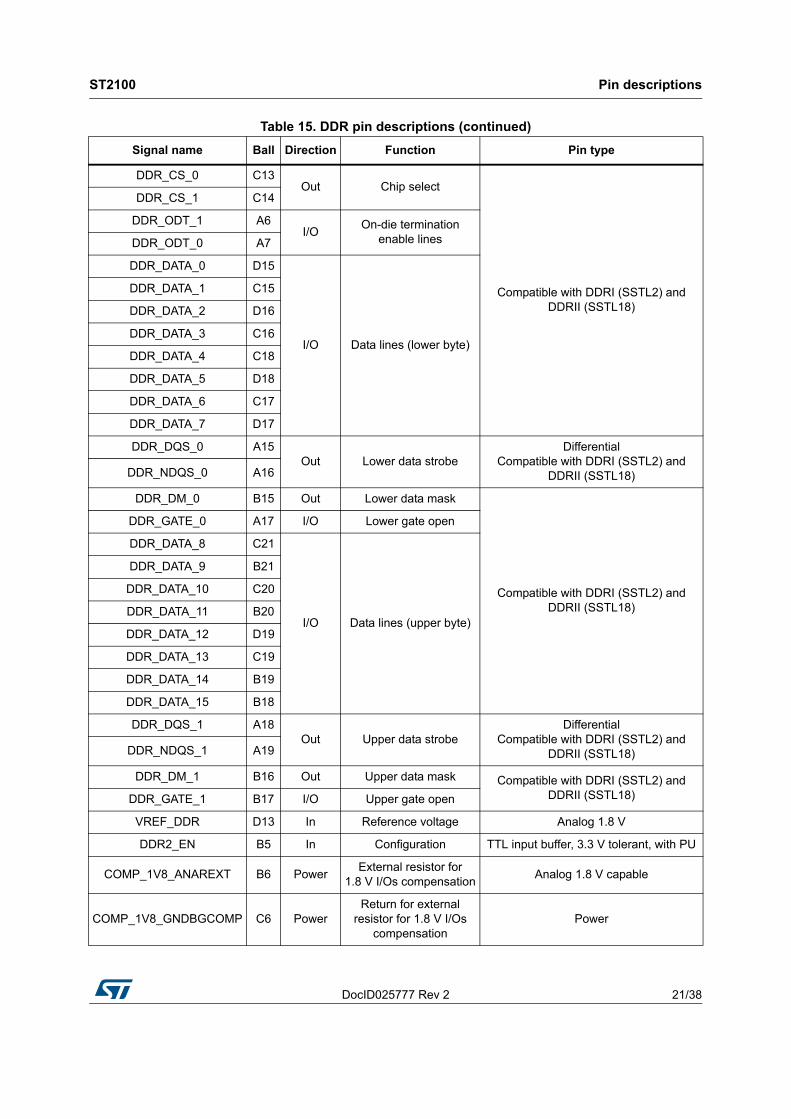
Table 15. DDR pin descriptions
Signal name Ball Direction Function Pin type
DDR_ADDR_0 D7
Out Address lines
Compatible with DDRI (SSTL2) and DDRII (SSTL18)
DDR_ADDR_1 C7
DDR_ADDR_2 B7
DDR_ADDR_3 A8
DDR_ADDR_4 B8
DDR_ADDR_5 C8
DDR_ADDR_6 D8
DDR_ADDR_7 A9
DDR_ADDR_8 B9
DDR_ADDR_9 C9
DDR_ADDR_10 D9
DDR_ADDR_11 A10
DDR_ADDR_12 B10
DDR_ADDR_13 C10
DDR_ADDR_14 D10
DDR_BA_0 C11
Out Bank selectDDR_BA_1 D12
DDR_BA_2 C12
DDR_RAS B14 Out Row address strobe
DDR_CAS B13 Out Column address strobe
DDR_WE B11 Out Write enable
DDR_CLKEN B12 Out Clock enable
DDR_CLK_P A12Out Differential clock
Differential Compatible with DDRI (SSTL2) and
DDRII (SSTL18)DDR_CLK_N A13
DocID025777 Rev 2 21/38
ST2100 Pin descriptions
38
DDR_CS_0 C13Out Chip select
Compatible with DDRI (SSTL2) and DDRII (SSTL18)
DDR_CS_1 C14
DDR_ODT_1 A6I/O
On-die termination enable linesDDR_ODT_0 A7
DDR_DATA_0 D15
I/O Data lines (lower byte)
DDR_DATA_1 C15
DDR_DATA_2 D16
DDR_DATA_3 C16
DDR_DATA_4 C18
DDR_DATA_5 D18
DDR_DATA_6 C17
DDR_DATA_7 D17
DDR_DQS_0 A15Out Lower data strobe
DifferentialCompatible with DDRI (SSTL2) and
DDRII (SSTL18)DDR_NDQS_0 A16
DDR_DM_0 B15 Out Lower data mask
Compatible with DDRI (SSTL2) and DDRII (SSTL18)
DDR_GATE_0 A17 I/O Lower gate open
DDR_DATA_8 C21
I/O Data lines (upper byte)
DDR_DATA_9 B21
DDR_DATA_10 C20
DDR_DATA_11 B20
DDR_DATA_12 D19
DDR_DATA_13 C19
DDR_DATA_14 B19
DDR_DATA_15 B18
DDR_DQS_1 A18Out Upper data strobe
DifferentialCompatible with DDRI (SSTL2) and
DDRII (SSTL18)DDR_NDQS_1 A19
DDR_DM_1 B16 Out Upper data mask Compatible with DDRI (SSTL2) and DDRII (SSTL18)DDR_GATE_1 B17 I/O Upper gate open
VREF_DDR D13 In Reference voltage Analog 1.8 V
DDR2_EN B5 In Configuration TTL input buffer, 3.3 V tolerant, with PU
COMP_1V8_ANAREXT B6 PowerExternal resistor for
1.8 V I/Os compensationAnalog 1.8 V capable
COMP_1V8_GNDBGCOMP C6 PowerReturn for external
resistor for 1.8 V I/Os compensation
Power
Table 15. DDR pin descriptions (continued)
Signal name Ball Direction Function Pin type
Pin descriptions ST2100
22/38 DocID025777 Rev 2
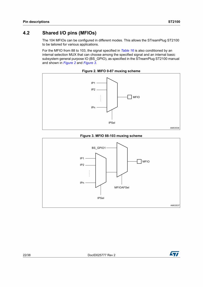
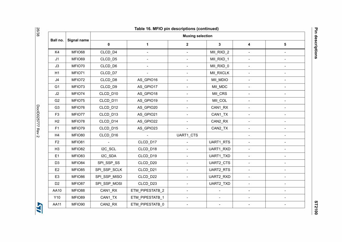
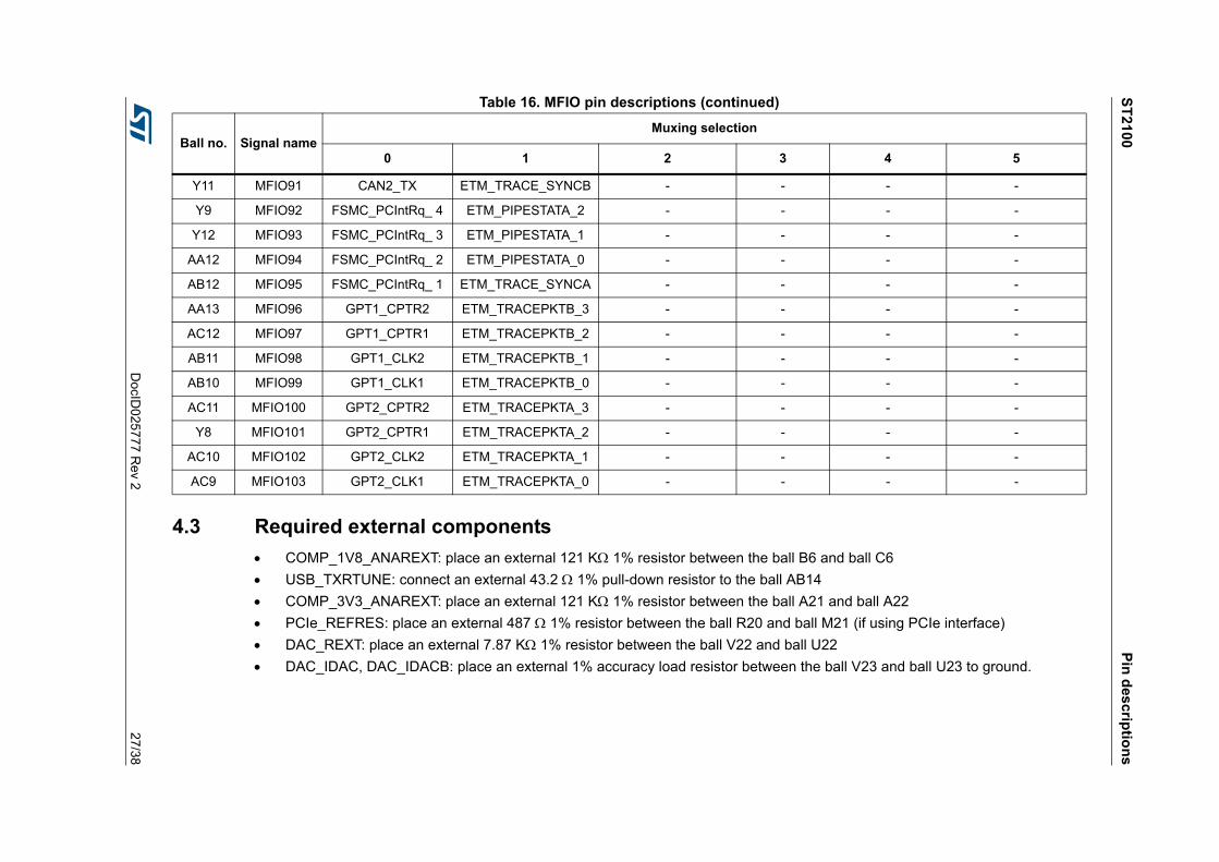
4.2 Shared I/O pins (MFIOs)
The 104 MFIOs can be configured in different modes. This allows the STreamPlug ST2100 to be tailored for various applications.
For the MFIO from 88 to 103, the signal specified in Table 16 is also conditioned by an internal selection MUX that can choose among the specified signal and an internal basic subsystem general purpose IO (BS_GPIO), as specified in the STreamPlug ST2100 manual and shown in Figure 2 and Figure 3.
Figure 2. MIFO 0-87 muxing scheme
Figure 3. MFIO 88-103 muxing scheme
ST
210
0P
in d
escrip
tion
s
Do
cID0
25777 R
ev 22
3/38
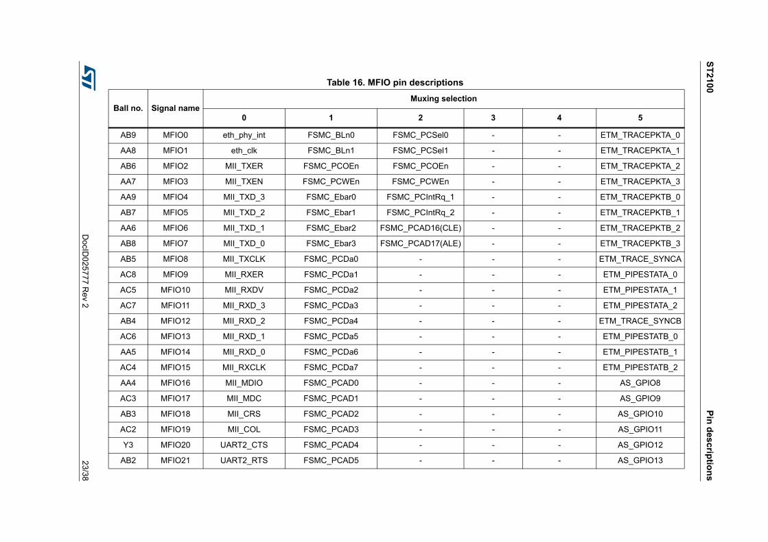
Table 16. MFIO pin descriptions
Ball no. Signal nameMuxing selection
0 1 2 3 4 5
AB9 MFIO0 eth_phy_int FSMC_BLn0 FSMC_PCSel0 - - ETM_TRACEPKTA_0
AA8 MFIO1 eth_clk FSMC_BLn1 FSMC_PCSel1 - - ETM_TRACEPKTA_1
AB6 MFIO2 MII_TXER FSMC_PCOEn FSMC_PCOEn - - ETM_TRACEPKTA_2
AA7 MFIO3 MII_TXEN FSMC_PCWEn FSMC_PCWEn - - ETM_TRACEPKTA_3
AA9 MFIO4 MII_TXD_3 FSMC_Ebar0 FSMC_PCIntRq_1 - - ETM_TRACEPKTB_0
AB7 MFIO5 MII_TXD_2 FSMC_Ebar1 FSMC_PCIntRq_2 - - ETM_TRACEPKTB_1
AA6 MFIO6 MII_TXD_1 FSMC_Ebar2 FSMC_PCAD16(CLE) - - ETM_TRACEPKTB_2
AB8 MFIO7 MII_TXD_0 FSMC_Ebar3 FSMC_PCAD17(ALE) - - ETM_TRACEPKTB_3
AB5 MFIO8 MII_TXCLK FSMC_PCDa0 - - - ETM_TRACE_SYNCA
AC8 MFIO9 MII_RXER FSMC_PCDa1 - - - ETM_PIPESTATA_0
AC5 MFIO10 MII_RXDV FSMC_PCDa2 - - - ETM_PIPESTATA_1
AC7 MFIO11 MII_RXD_3 FSMC_PCDa3 - - - ETM_PIPESTATA_2
AB4 MFIO12 MII_RXD_2 FSMC_PCDa4 - - - ETM_TRACE_SYNCB
AC6 MFIO13 MII_RXD_1 FSMC_PCDa5 - - - ETM_PIPESTATB_0
AA5 MFIO14 MII_RXD_0 FSMC_PCDa6 - - - ETM_PIPESTATB_1
AC4 MFIO15 MII_RXCLK FSMC_PCDa7 - - - ETM_PIPESTATB_2
AA4 MFIO16 MII_MDIO FSMC_PCAD0 - - - AS_GPIO8
AC3 MFIO17 MII_MDC FSMC_PCAD1 - - - AS_GPIO9
AB3 MFIO18 MII_CRS FSMC_PCAD2 - - - AS_GPIO10
AC2 MFIO19 MII_COL FSMC_PCAD3 - - - AS_GPIO11
Y3 MFIO20 UART2_CTS FSMC_PCAD4 - - - AS_GPIO12
AB2 MFIO21 UART2_RTS FSMC_PCAD5 - - - AS_GPIO13
Pin
de
scrip
tion
sS
T21
00
24/38D
ocID
02577
7 Rev 2
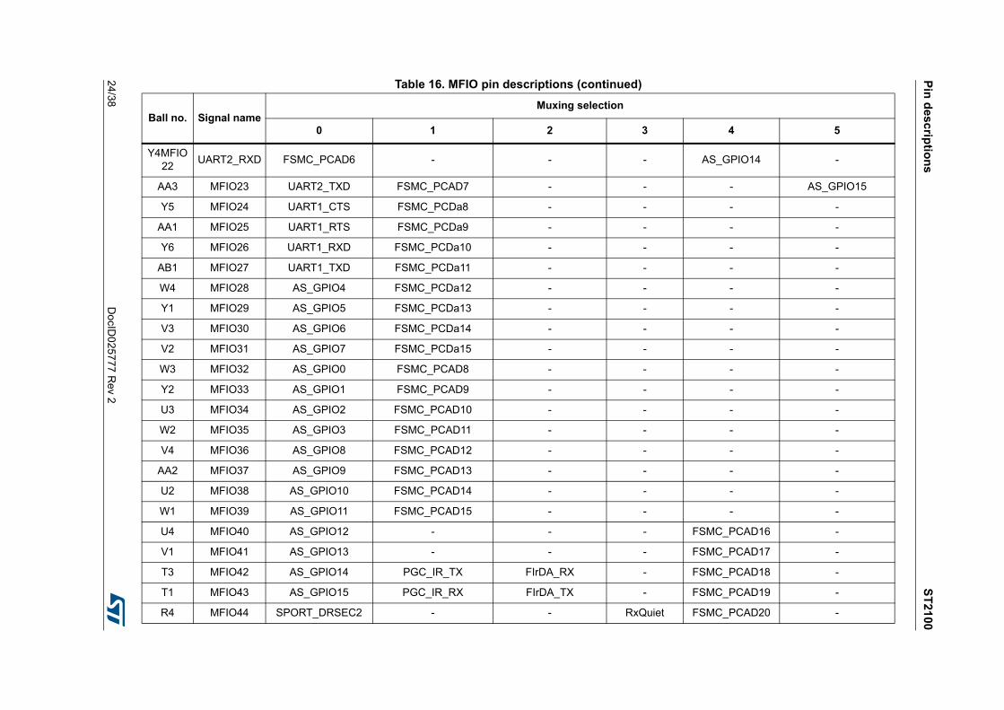
Y4MFIO22
UART2_RXD FSMC_PCAD6 - - - AS_GPIO14 -
AA3 MFIO23 UART2_TXD FSMC_PCAD7 - - - AS_GPIO15
Y5 MFIO24 UART1_CTS FSMC_PCDa8 - - - -
AA1 MFIO25 UART1_RTS FSMC_PCDa9 - - - -
Y6 MFIO26 UART1_RXD FSMC_PCDa10 - - - -
AB1 MFIO27 UART1_TXD FSMC_PCDa11 - - - -
W4 MFIO28 AS_GPIO4 FSMC_PCDa12 - - - -
Y1 MFIO29 AS_GPIO5 FSMC_PCDa13 - - - -
V3 MFIO30 AS_GPIO6 FSMC_PCDa14 - - - -
V2 MFIO31 AS_GPIO7 FSMC_PCDa15 - - - -
W3 MFIO32 AS_GPIO0 FSMC_PCAD8 - - - -
Y2 MFIO33 AS_GPIO1 FSMC_PCAD9 - - - -
U3 MFIO34 AS_GPIO2 FSMC_PCAD10 - - - -
W2 MFIO35 AS_GPIO3 FSMC_PCAD11 - - - -
V4 MFIO36 AS_GPIO8 FSMC_PCAD12 - - - -
AA2 MFIO37 AS_GPIO9 FSMC_PCAD13 - - - -
U2 MFIO38 AS_GPIO10 FSMC_PCAD14 - - - -
W1 MFIO39 AS_GPIO11 FSMC_PCAD15 - - - -
U4 MFIO40 AS_GPIO12 - - - FSMC_PCAD16 -
V1 MFIO41 AS_GPIO13 - - - FSMC_PCAD17 -
T3 MFIO42 AS_GPIO14 PGC_IR_TX FIrDA_RX - FSMC_PCAD18 -
T1 MFIO43 AS_GPIO15 PGC_IR_RX FIrDA_TX - FSMC_PCAD19 -
R4 MFIO44 SPORT_DRSEC2 - - RxQuiet FSMC_PCAD20 -
Table 16. MFIO pin descriptions (continued)
Ball no. Signal nameMuxing selection
0 1 2 3 4 5
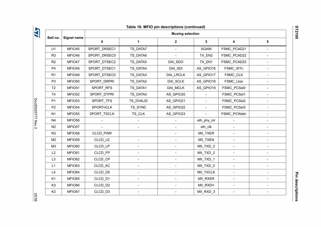
ST
210
0P
in d
escrip
tion
s
Do
cID0
25777 R
ev 22
5/38
U1 MFIO45 SPORT_DRSEC1 TS_DATA7 - XGAIN FSMC_PCAD21 -
R3 MFIO46 SPORT_DRSEC0 TS_DATA6 - TX_EN2 FSMC_PCAD22 -
R2 MFIO47 SPORT_DTSEC2 TS_DATA5 DAI_SDO TX_EN1 FSMC_PCAD23 -
P4 MFIO48 SPORT_DTSEC1 TS_DATA4 DAI_SDI AS_GPIO16 FSMC_WTn -
R1 MFIO49 SPORT_DTSEC0 TS_DATA3 DAI_LRCLK AS_GPIO17 FSMC_CLK -
P3 MFIO50 SPORT_DRPRI TS_DATA2 DAI_SCLK AS_GPIO18 FSMC_Lbar -
T2 MFIO51 SPORT_RFS TS_DATA1 DAI_MCLK AS_GPIO19 FSMC_PCSel0 -
T4 MFIO52 SPORT_DTPRI TS_DATA0 AS_GPIO20 - FSMC_PCSel1 -
P1 MFIO53 SPORT_TFS TS_DVALID AS_GPIO21 - FSMC_PCSel2 -
P2 MFIO54 SPORTnCLK TS_SYNC AS_GPIO22 - FSMC_PCSel3 -
N1 MFIO55 SPORT_TSCLK TS_CLK AS_GPIO23 - FSMC_PCWaitn -
N4 MFIO56 - - - eth_phy_int - -
N2 MFIO57 - - - eth_clk - -
N3 MFIO58 CLCD_PWR - MII_TXER - -
M2 MFIO59 CLCD_LE - - MII_TXEN - -
M3 MFIO60 CLCD_LP - - MII_TXD_3 - -
L2 MFIO61 CLCD_FP - - MII_TXD_2 - -
L3 MFIO62 CLCD_CP - - MII_TXD_1 - -
L1 MFIO63 CLCD_AC - - MII_TXD_0 - -
L4 MFIO64 CLCD_D0 - - MII_TXCLK - -
K1 MFIO65 CLCD_D1 - - MII_RXER - -
K3 MFIO66 CLCD_D2 - - MII_RXDV - -
K2 MFIO67 CLCD_D3 - - MII_RXD_3 - -
Table 16. MFIO pin descriptions (continued)
Ball no. Signal nameMuxing selection
0 1 2 3 4 5
Pin
de
scrip
tion
sS
T21
00
26/38D
ocID
02577
7 Rev 2
K4 MFIO68 CLCD_D4 - - MII_RXD_2 - -
J1 MFIO69 CLCD_D5 - - MII_RXD_1 - -
J3 MFIO70 CLCD_D6 - - MII_RXD_0 - -
H1 MFIO71 CLCD_D7 - - MII_RXCLK - -
J4 MFIO72 CLCD_D8 AS_GPIO16 - MII_MDIO - -
G1 MFIO73 CLCD_D9 AS_GPIO17 - MII_MDC - -
J2 MFIO74 CLCD_D10 AS_GPIO18 - MII_CRS - -
G2 MFIO75 CLCD_D11 AS_GPIO19 - MII_COL - -
G3 MFIO76 CLCD_D12 AS_GPIO20 - CAN1_RX - -
F3 MFIO77 CLCD_D13 AS_GPIO21 - CAN1_TX - -
H2 MFIO78 CLCD_D14 AS_GPIO22 - CAN2_RX - -
F1 MFIO79 CLCD_D15 AS_GPIO23 - CAN2_TX - -
H4 MFIO80 CLCD_D16 - UART1_CTS - -
F2 MFIO81 - CLCD_D17 - UART1_RTS - -
H3 MFIO82 I2C_SCL CLCD_D18 - UART1_RXD - -
E1 MFIO83 I2C_SDA CLCD_D19 - UART1_TXD - -
D3 MFIO84 SPI_SSP_SS CLCD_D20 - UART2_CTS - -
E2 MFIO85 SPI_SSP_SCLK CLCD_D21 - UART2_RTS - -
E3 MFIO86 SPI_SSP_MISO CLCD_D22 - UART2_RXD - -
D2 MFIO87 SPI_SSP_MOSI CLCD_D23 - UART2_TXD - -
AA10 MFIO88 CAN1_RX ETM_PIPESTATB_2 - - - -
Y10 MFIO89 CAN1_TX ETM_PIPESTATB_1 - - - -
AA11 MFIO90 CAN2_RX ETM_PIPESTATB_0 - - - -
Table 16. MFIO pin descriptions (continued)
Ball no. Signal nameMuxing selection
0 1 2 3 4 5
ST
210
0P
in d
escrip
tion
s
Do
cID0
25777 R
ev 22
7/38
4.3 Required external components
COMP_1V8_ANAREXT: place an external 121 K 1% resistor between the ball B6 and ball C6
USB_TXRTUNE: connect an external 43.2 1% pull-down resistor to the ball AB14
COMP_3V3_ANAREXT: place an external 121 K 1% resistor between the ball A21 and ball A22
PCIe_REFRES: place an external 487 1% resistor between the ball R20 and ball M21 (if using PCIe interface)
DAC_REXT: place an external 7.87 K 1% resistor between the ball V22 and ball U22
DAC_IDAC, DAC_IDACB: place an external 1% accuracy load resistor between the ball V23 and ball U23 to ground.
Y11 MFIO91 CAN2_TX ETM_TRACE_SYNCB - - - -
Y9 MFIO92 FSMC_PCIntRq_ 4 ETM_PIPESTATA_2 - - - -
Y12 MFIO93 FSMC_PCIntRq_ 3 ETM_PIPESTATA_1 - - - -
AA12 MFIO94 FSMC_PCIntRq_ 2 ETM_PIPESTATA_0 - - - -
AB12 MFIO95 FSMC_PCIntRq_ 1 ETM_TRACE_SYNCA - - - -
AA13 MFIO96 GPT1_CPTR2 ETM_TRACEPKTB_3 - - - -
AC12 MFIO97 GPT1_CPTR1 ETM_TRACEPKTB_2 - - - -
AB11 MFIO98 GPT1_CLK2 ETM_TRACEPKTB_1 - - - -
AB10 MFIO99 GPT1_CLK1 ETM_TRACEPKTB_0 - - - -
AC11 MFIO100 GPT2_CPTR2 ETM_TRACEPKTA_3 - - - -
Y8 MFIO101 GPT2_CPTR1 ETM_TRACEPKTA_2 - - - -
AC10 MFIO102 GPT2_CLK2 ETM_TRACEPKTA_1 - - - -
AC9 MFIO103 GPT2_CLK1 ETM_TRACEPKTA_0 - - - -
Table 16. MFIO pin descriptions (continued)
Ball no. Signal nameMuxing selection
0 1 2 3 4 5
Memory map ST2100
28/38 DocID025777 Rev 2
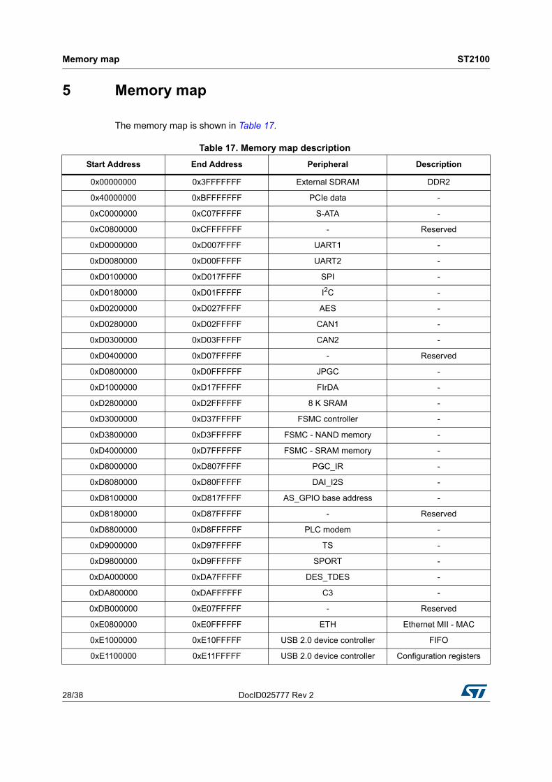
5 Memory map
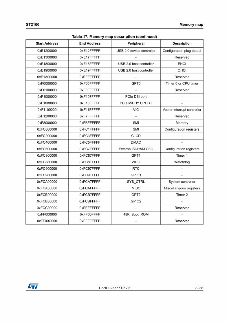
The memory map is shown in Table 17.
Table 17. Memory map description
Start Address End Address Peripheral Description
0x00000000 0x3FFFFFFF External SDRAM DDR2
0x40000000 0xBFFFFFFF PCIe data -
0xC0000000 0xC07FFFFF S-ATA -
0xC0800000 0xCFFFFFFF - Reserved
0xD0000000 0xD007FFFF UART1 -
0xD0080000 0xD00FFFFF UART2 -
0xD0100000 0xD017FFFF SPI -
0xD0180000 0xD01FFFFF I2C -
0xD0200000 0xD027FFFF AES -
0xD0280000 0xD02FFFFF CAN1 -
0xD0300000 0xD03FFFFF CAN2 -
0xD0400000 0xD07FFFFF - Reserved
0xD0800000 0xD0FFFFFF JPGC -
0xD1000000 0xD17FFFFF FIrDA -
0xD2800000 0xD2FFFFFF 8 K SRAM -
0xD3000000 0xD37FFFFF FSMC controller -
0xD3800000 0xD3FFFFFF FSMC - NAND memory -
0xD4000000 0xD7FFFFFF FSMC - SRAM memory -
0xD8000000 0xD807FFFF PGC_IR -
0xD8080000 0xD80FFFFF DAI_I2S -
0xD8100000 0xD817FFFF AS_GPIO base address -
0xD8180000 0xD87FFFFF - Reserved
0xD8800000 0xD8FFFFFF PLC modem -
0xD9000000 0xD97FFFFF TS -
0xD9800000 0xD9FFFFFF SPORT -
0xDA000000 0xDA7FFFFF DES_TDES -
0xDA800000 0xDAFFFFFF C3 -
0xDB000000 0xE07FFFFF - Reserved
0xE0800000 0xE0FFFFFF ETH Ethernet MII - MAC
0xE1000000 0xE10FFFFF USB 2.0 device controller FIFO
0xE1100000 0xE11FFFFF USB 2.0 device controller Configuration registers
DocID025777 Rev 2 29/38
ST2100 Memory map
38
0xE1200000 0xE12FFFFF USB 2.0 device controller Configuration plug detect
0xE1300000 0xE17FFFFF - Reserved
0xE1800000 0xE18FFFFF USB 2.0 host controller EHCI
0xE1900000 0xE19FFFFF USB 2.0 host controller OHCI
0xE1A00000 0xEFFFFFFF - Reserved
0xF0000000 0xF00FFFFF GPT0 Timer 0 or CPU timer
0xF0100000 0xF0FFFFFF - Reserved
0xF1000000 0xF107FFFF PCIe DBI port -
0xF1080000 0xF10FFFFF PCIe MiPHY UPORT -
0xF1100000 0xF11FFFFF VIC Vector interrupt controller
0xF1200000 0xF7FFFFFF - Reserved
0xF8000000 0xFBFFFFFF SMI Memory
0xFC000000 0xFC1FFFFF SMI Configuration registers
0xFC200000 0xFC3FFFFF CLCD -
0xFC400000 0xFC5FFFFF DMAC -
0xFC600000 0xFC7FFFFF External SDRAM CFG Configuration registers
0xFC800000 0xFC87FFFF GPT1 Timer 1
0xFC880000 0xFC8FFFFF WDG Watchdog
0xFC900000 0xFC97FFFF RTC -
0xFC980000 0xFC9FFFFF GPIO1 -
0xFCA00000 0xFCA7FFFF SYS_CTRL System controller
0xFCA80000 0xFCAFFFFF MISC Miscellaneous registers
0xFCB00000 0xFCB7FFFF GPT2 Timer 2
0xFCB80000 0xFCBFFFFF GPIO2 -
0xFCC00000 0xFEFFFFFF - Reserved
0xFF000000 0xFF00FFFF 48K_Boot_ROM -
0xFF00C000 0xFFFFFFFF - Reserved
Table 17. Memory map description (continued)
Start Address End Address Peripheral Description
Clocking parameters ST2100
30/38 DocID025777 Rev 2
6 Clocking parameters
This section details clock related electrical specifications.
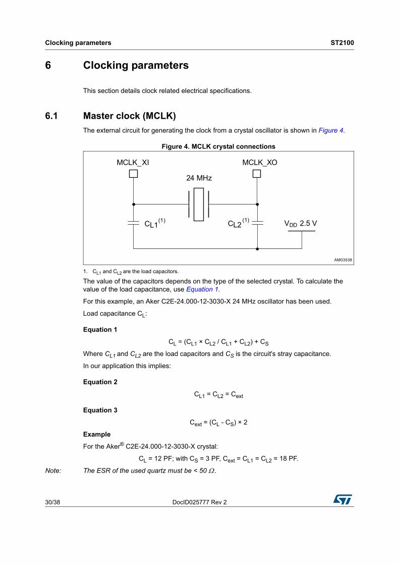
6.1 Master clock (MCLK)
The external circuit for generating the clock from a crystal oscillator is shown in Figure 4.
Figure 4. MCLK crystal connections
1. CL1 and CL2 are the load capacitors.
The value of the capacitors depends on the type of the selected crystal. To calculate the value of the load capacitance, use Equation 1.
For this example, an Aker C2E-24.000-12-3030-X 24 MHz oscillator has been used.
Load capacitance CL:
Equation 1
CL = (CL1 × CL2 / CL1 + CL2) + CS
Where CL1 and CL2 are the load capacitors and CS is the circuit's stray capacitance.
In our application this implies:
Equation 2
CL1 = CL2 = Cext
Equation 3
Cext = (CL - CS) × 2
Example
For the Aker® C2E-24.000-12-3030-X crystal:
CL = 12 PF; with CS = 3 PF, Cext = CL1 = CL2 = 18 PF.
Note: The ESR of the used quartz must be < 50 .
DocID025777 Rev 2 31/38
ST2100 Clocking parameters
38
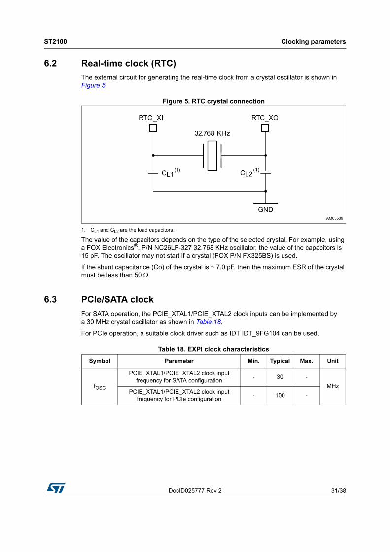
6.2 Real-time clock (RTC)
The external circuit for generating the real-time clock from a crystal oscillator is shown in Figure 5.
Figure 5. RTC crystal connection
1. CL1 and CL2 are the load capacitors.
The value of the capacitors depends on the type of the selected crystal. For example, using a FOX Electronics®, P/N NC26LF-327 32.768 KHz oscillator, the value of the capacitors is 15 pF. The oscillator may not start if a crystal (FOX P/N FX325BS) is used.
If the shunt capacitance (Co) of the crystal is ~ 7.0 pF, then the maximum ESR of the crystal must be less than 50 .
6.3 PCIe/SATA clock
For SATA operation, the PCIE_XTAL1/PCIE_XTAL2 clock inputs can be implemented by a 30 MHz crystal oscillator as shown in Table 18.
For PCIe operation, a suitable clock driver such as IDT IDT_9FG104 can be used.
Table 18. EXPI clock characteristics
Symbol Parameter Min. Typical Max. Unit
fOSC
PCIE_XTAL1/PCIE_XTAL2 clock input frequency for SATA configuration
- 30 -
MHzPCIE_XTAL1/PCIE_XTAL2 clock input
frequency for PCIe configuration- 100 -
Electrical characteristics ST2100
32/38 DocID025777 Rev 2
7 Electrical characteristics
This section provides electrical specifications for the STreamPlug ST2100 device.
7.1 Absolute maximum ratings
This product contains devices to protect the inputs against damage due to high/low static voltages. However it is advisable to take normal precaution to avoid application of any voltage higher/lower than the specified maximum/minimum rated voltages.
The absolute maximum ratings shown in Table 19 are the maximum stress that can be applied to a device without causing permanent damage. However, extended exposure to minimum/maximum ratings may affect long term device reliability.
7.2 Power consumption
In Table 20 and Table 21 power consumption data are based on bench measurements with devices using the Linux OS, the CPU and DDR2 running at 333 MHz and all on-chip peripherals and internal modules enabled while the STreamPlug ST2100 is transferring a file from the USB Flash memory to the powerline.
Table 19. Absolute maximum rating
Symbol Parameter Min. Max. Unit
VDD1.2 Supply voltage for the core -0.3 1.32 V
VDD3.3 Supply voltage for the I/Os -0.3 3.63 V
VDD2.5 Supply voltage for the DDR/AFE -0.3 2.75 V
VDD1.5 Supply voltage for the real-time clock -0.3 2.75 V
TSTG Storage temperature -55 150 °C
TJ Junction temperature -40 125 °C
Table 20. Power consumption
Symbol Parameter Typical Unit
PD (core supply) Power consumption of 1.2 V supply voltage for the core 460 mW
PD (IO supply) Power consumption of 3.3 V supply voltage for the I/Os 270 mW
PD (AFE supply) Power consumption of 2.5 V supply voltage 260 mW
PD (DDR supply)Power consumption of 1.8 V supply voltage for the DDR
interface170 mW
PD (RTC supply) Power consumption of 1.5 V supply voltage for the RTC 9 W
DocID025777 Rev 2 33/38
ST2100 Electrical characteristics
38
7.3 DC electrical characteristics
The recommended operating conditions are listed in Table 22 and Table 23.
Thermal simulations should be done to verify if additional cooling is required. These simulations should take into account power consumption, PCB dissipation, air flow and/or heatsinks. The STreamPlug device can perform correctly above the specified ambient temperature range if the maximum junction temperature remains below 125 °C.
Table 21. Power consumption using 2.5 V internal LDO
Symbol Parameter Typical Unit
PD (core supply) Power consumption of 1.2 V supply voltage for the core 460 mW
PD (IO supply) Power consumption of 3.3 V supply voltage for the I/Os 630 mW
PD (DDR supply)Power consumption of 1.8 V supply voltage for the DDR
interface170 mW
PD (RTC supply) Power consumption of 1.5 V supply voltage for the RTC 9 µW
Table 22. Recommended operating conditions
Symbol Parameter Min. Typical Max. Unit
VDD1.2 Supply voltage for the core 1.08 1.2 1.32 V
VDD3.3 Supply voltage for the I/Os 2.97 3.3 3.63 V
VDD2.5 Supply voltage for the analog peripherals 2.25 2.5 2.75 V
VDD1.8/2.5 Supply voltage for the DDR -10% 2.5 V / 1.8 V +10% V
VDD1.5 Supply voltage for the RTC 1.3 1.5 2.0 V
VDD3.3 REG Supply voltage for 2.5 V linear regulator 2,97 3.3 3.63 V
Table 23. Thermal recommended ratings
Symbol Parameter Min. Max. Unit
TSTG Storage temperature range -55 150 °C
TJ Junction temperature -40 125 -
Ta Ambient temperature -40 85 -
Electrical characteristics ST2100
34/38 DocID025777 Rev 2
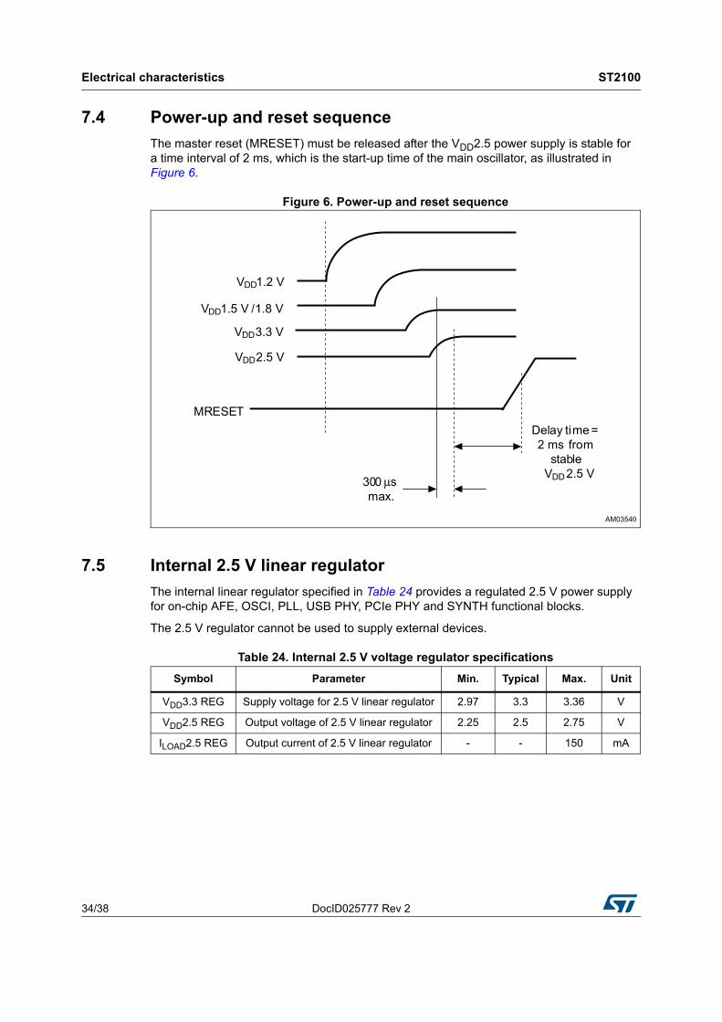
7.4 Power-up and reset sequence
The master reset (MRESET) must be released after the VDD2.5 power supply is stable for a time interval of 2 ms, which is the start-up time of the main oscillator, as illustrated in Figure 6.
Figure 6. Power-up and reset sequence
7.5 Internal 2.5 V linear regulator
The internal linear regulator specified in Table 24 provides a regulated 2.5 V power supply for on-chip AFE, OSCI, PLL, USB PHY, PCIe PHY and SYNTH functional blocks.
The 2.5 V regulator cannot be used to supply external devices.
Table 24. Internal 2.5 V voltage regulator specifications
Symbol Parameter Min. Typical Max. Unit
VDD3.3 REG Supply voltage for 2.5 V linear regulator 2.97 3.3 3.36 V
VDD2.5 REG Output voltage of 2.5 V linear regulator 2.25 2.5 2.75 V
ILOAD2.5 REG Output current of 2.5 V linear regulator - - 150 mA
DocID025777 Rev 2 35/38
ST2100 Package information
38
8 Package information
In order to meet environmental requirements, ST offers these devices in different grades of ECOPACK® packages, depending on their level of environmental compliance. ECOPACK specifications, grade definitions and product status are available at: www.st.com. ECOPACK is an ST trademark.
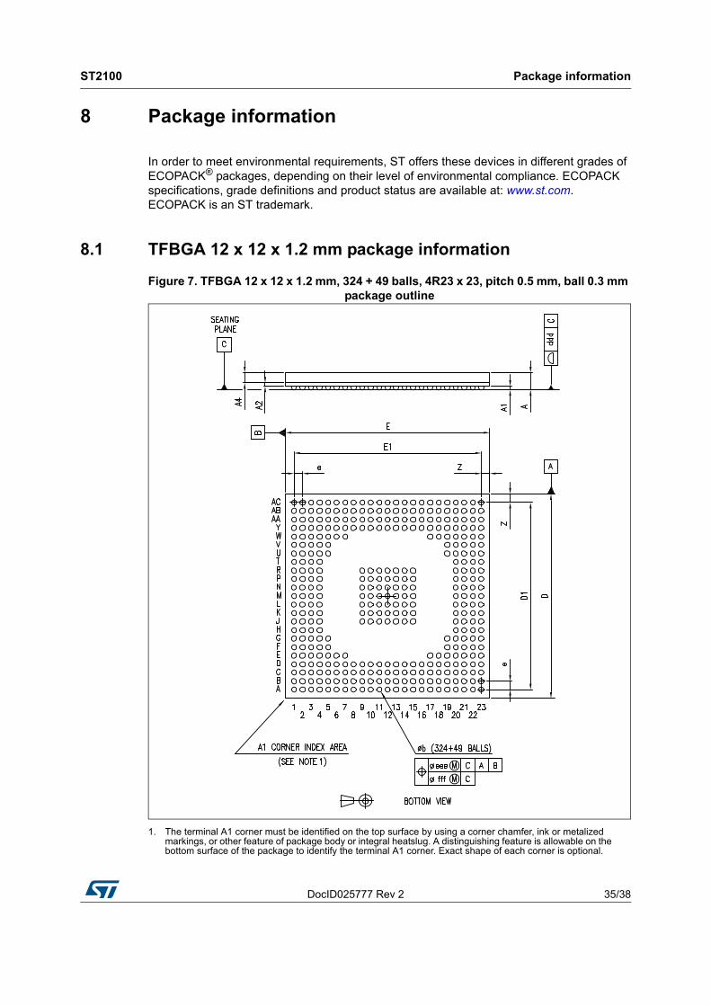
8.1 TFBGA 12 x 12 x 1.2 mm package information
Figure 7. TFBGA 12 x 12 x 1.2 mm, 324 + 49 balls, 4R23 x 23, pitch 0.5 mm, ball 0.3 mm package outline
1. The terminal A1 corner must be identified on the top surface by using a corner chamfer, ink or metalized markings, or other feature of package body or integral heatslug. A distinguishing feature is allowable on the bottom surface of the package to identify the terminal A1 corner. Exact shape of each corner is optional.
Package information ST2100
36/38 DocID025777 Rev 2
Table 25 lists the mechanical data for the package shown in Figure 7.
The TFBGA (“Thin profile Fine Pitch Ball Grid Array”) package uses a grid of solder balls as its connectors. The TFBGA package is noted for its compact size, high lead count and low inductance, which allows lower voltages to be used.
Table 26 lists thermal characteristics for the TFGBA package.
Table 25. TFBGA 12 x 12 x 1.2 mm, 324 + 49 balls, 4R23 x 23, pitch 0.5 mm, ball 0.3 mm package mechanical data
SymbolDimensions (mm)
NoteMin. Typical Max.
A - - 1.20 (1)
1. The total profile height (dim. A) is measured from the seating plane to the top of the component.The maximum total package height is calculated by the following methodology:A1 typ. + A2 typ. + A3 typ. + (A12 + A22 + A32 tolerance values).
Thin profile: 1.00 < A . 1.20 mm / fine pitch: e < 1.00 mm pitch.
A1 0.15 - - -
A2 - 0.20 - -
A4 - 0.585 - -
b 0.25 0.30 0.35 (2)
2. The typical ball diameter before mounting is 0.30 mm.
D 11.85 12.00 12.15 -
D1 - 11.00 - -
E 11.85 12.00 12.15 -
E1 - 11.00 - -
e - 0.50 - -
Z - 0.50 - -
ddd - - 0.08 -
eee - - 0.15 (3)
3. The tolerance of position that controls the location of the pattern of balls with respect to datums A and B. For each ball there is a cylindrical tolerance zone “eee” perpendicular to datum “C” and located on true position with respect to datums “A” and “B” as defined by “e”. The axis perpendicular to datum “C” of each ball must lie within this tolerance zone.
fff - - 0.05 (4)
4. The tolerance of position that controls the location of the balls within the matrix with respect to each other. For each ball there is a cylindrical tolerance zone “fff” perpendicular to datum “C” and located on true position as defined by “e”. The axis perpendicular to datum “C” of each ball must lie within this tolerance zone. Each tolerance zone “fff” in the array is contained entirely in the respective zone “eee” above. The axis of each ball must lie simultaneously in both tolerance zones.
Table 26. TFGBA package thermal characteristics
Symbol Parameter Value Unit
JA(1)
1. Measured on a JESD51 2S2P test board.
Thermal resistance junction to ambient 33 °C/W
DocID025777 Rev 2 37/38
ST2100 Revision history
38
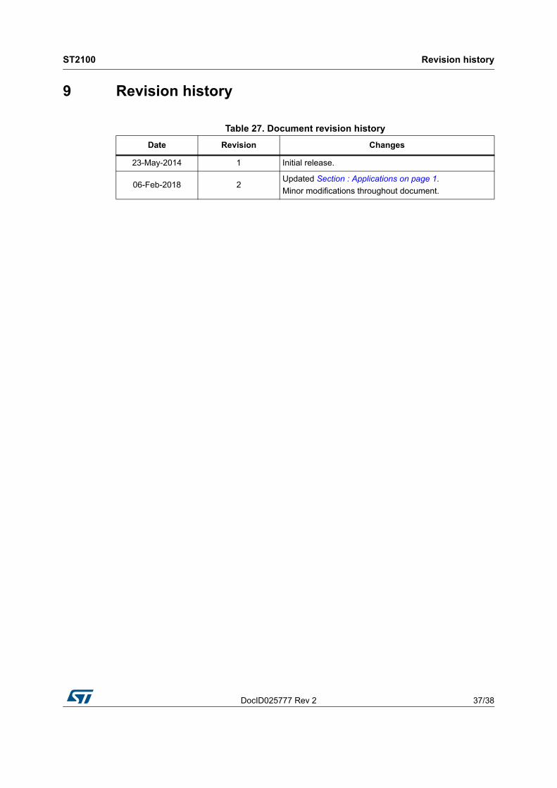
9 Revision history
Table 27. Document revision history
Date Revision Changes
23-May-2014 1 Initial release.
06-Feb-2018 2Updated Section : Applications on page 1.
Minor modifications throughout document.
ST2100
38/38 DocID025777 Rev 2
IMPORTANT NOTICE – PLEASE READ CAREFULLY
STMicroelectronics NV and its subsidiaries (“ST”) reserve the right to make changes, corrections, enhancements, modifications, and improvements to ST products and/or to this document at any time without notice. Purchasers should obtain the latest relevant information on ST products before placing orders. ST products are sold pursuant to ST’s terms and conditions of sale in place at the time of order acknowledgement.
Purchasers are solely responsible for the choice, selection, and use of ST products and ST assumes no liability for application assistance or the design of Purchasers’ products.
No license, express or implied, to any intellectual property right is granted by ST herein.
Resale of ST products with provisions different from the information set forth herein shall void any warranty granted by ST for such product.
ST and the ST logo are trademarks of ST. All other product or service names are the property of their respective owners.
Information in this document supersedes and replaces information previously supplied in any prior versions of this document.
© 2018 STMicroelectronics – All rights reserved