Broadband High Efficiency Fractal-Like and Diverse ...
150
University of Arkansas, Fayeeville ScholarWorks@UARK eses and Dissertations 7-2015 Broadband High Efficiency Fractal-Like and Diverse Geometry Silicon Nanowire Arrays for Photovoltaic Applications Omar Hassan Al-Zoubi University of Arkansas, Fayeeville Follow this and additional works at: hp://scholarworks.uark.edu/etd Part of the Nanoscience and Nanotechnology Commons , Nanotechnology Fabrication Commons , and the Power and Energy Commons is Dissertation is brought to you for free and open access by ScholarWorks@UARK. It has been accepted for inclusion in eses and Dissertations by an authorized administrator of ScholarWorks@UARK. For more information, please contact [email protected], [email protected]. Recommended Citation Al-Zoubi, Omar Hassan, "Broadband High Efficiency Fractal-Like and Diverse Geometry Silicon Nanowire Arrays for Photovoltaic Applications" (2015). eses and Dissertations. 1258. hp://scholarworks.uark.edu/etd/1258
Transcript of Broadband High Efficiency Fractal-Like and Diverse ...

University of Arkansas, FayettevilleScholarWorks@UARK
Theses and Dissertations
7-2015
Broadband High Efficiency Fractal-Like andDiverse Geometry Silicon Nanowire Arrays forPhotovoltaic ApplicationsOmar Hassan Al-ZoubiUniversity of Arkansas, Fayetteville
Follow this and additional works at: http://scholarworks.uark.edu/etd
Part of the Nanoscience and Nanotechnology Commons, Nanotechnology FabricationCommons, and the Power and Energy Commons
This Dissertation is brought to you for free and open access by ScholarWorks@UARK. It has been accepted for inclusion in Theses and Dissertations byan authorized administrator of ScholarWorks@UARK. For more information, please contact [email protected], [email protected].
Recommended CitationAl-Zoubi, Omar Hassan, "Broadband High Efficiency Fractal-Like and Diverse Geometry Silicon Nanowire Arrays for PhotovoltaicApplications" (2015). Theses and Dissertations. 1258.http://scholarworks.uark.edu/etd/1258

Broadband High Efficiency Fractal-Like and Diverse Geometry Silicon Nanowire Arrays for
Photovoltaic Applications
A dissertation submitted in partial fulfillment
of the requirements for the degree of
Doctor of Philosophy in Electrical Engineering
by
Omar H. AL-Zoubi
Mu’tah University
Bachelor of Science in Electrical Engineering, 1994
Yarmouk University
Master of Science in Electrical Engineering, 2009
July 2015
University of Arkansas
The dissertation is approved for recommendation to the Graduate Council.
Dr. Hameed A. Naseem
Dissertation Director
Dr. Samir M. EL-Ghazaly
Committee Member
Dr. Surendra P. Singh
Committee Member
Dr. Shui-Qing (Fisher) Yu
Committee Member
Dr. Reeta Vyas
Committee Member

ABSTRACT
Solar energy has many advantages over conventional sources of energy. It is abundant,
clean and sustainable. One way to convert solar energy directly into electrical energy is by using
the photovoltaic solar cells (PVSC). Despite PVSC are becoming economically competitive, they
still have high cost and low light to electricity conversion efficiency. Therefore, increasing the
efficiency and reducing the cost are key elements for producing economically more competitive
PVSC that would have significant impact on energy market and saving environment. A
significant percentage of the PVSC cost is due to the materials cost. For that, thin films PVSC
have been proposed which offer the benefits of the low amount of material and fabrication costs.
Regrettably, thin film PVSC show poor light to electricity conversion efficiency because of
many factors especially the high optical losses. To enhance conversion efficiency, numerous
techniques have been proposed to reduce the optical losses and to enhance the absorption of light
in thin film PVSC. One promising technique is the nanowire (NW) arrays in general and the
silicon nanowire (SiNW) arrays in particular.
The purpose of this research is to introduce vertically aligned SiNW arrays with
enhanced and broadband absorption covering the entire solar spectrum while simultaneously
reducing the amount of material used. To this end, we apply new concept for designing SiNW
arrays based on employing diversity of physical dimensions, especially radial diversity within
certain lattice configurations. In order to study the interaction of light with SiNW arrays and
compute their optical properties, electromagnetic numerical modeling is used. A commercial
numerical electromagnetic solver software package, high frequency structure simulation (HFSS),
is utilized to model the SiNW arrays and to study their optical properties.
We studied different geometries factors that affect the optical properties of SiNW arrays.
Based on this study, we found that the optical properties of SiNW arrays are strongly affected by
the radial diversity, the arrangement of SiNW in a lattice, and the configuration of such lattice.
The proper selection of these parameters leads to broaden and enhance the light absorption of the
SiNW arrays. Inspired by natural configurations, fractal geometry and diamond lattice structures,
we introduced two lattice configurations: fractal-like array (FLA) that is inspired by fractal
geometry, and diamond-like array (DLA) that is inspired by diamond crystal lattice structure.
Optimization, using parametric analysis, of the introduced arrays parameters for the light
absorption level and the amount of used material has been performed. Both of the introduced
SiNW arrays show broadband, strong light absorption coupled with reduction of the amount of
the used material. DLA in specific showed significantly enhanced absorption covering the entire
solar spectrum of interest, where near-unity absorption spectrum could be achieved.
We studied the optical properties of complete PVSC devices that are based on SiNW
array. Moreover, the performance of PVSC device that is based on SiNW has been investigated
by using numerical modeling. SILVACO software package is used for performing the numerical
simulation of the PVSC device performance, which can simultaneously handle the different
coupled physical mechanisms contributing to the photovoltaic effect. The effect of the geometry
of PVSC device that is based on SiNW is investigated, which shows that the geometry of such
PVSC has a role in enhancing its electrical properties.
The outcome of this study introduces new SiNW array configurations that have enhanced
optical properties using a low amount of material that can be utilized for producing higher
efficiency thin film PVCS.

The overall conclusion of this work is that a weak absorption indirect band gap material,
silicon, in the form of properly designed SiNW and SiNC arrays has the potentials to achieve
near-unity ideal absorption spectrum using reduced amount of material, which can lead to
produce new generation of lower cost and enhanced efficiency thin film PVSC.

©2015 by Omar H. AL-Zoubi
All Rights Reserved

ACKNOWLEDGEMNT
First and foremost, I want to thank my advisor Professor Hameed Naseem. It has been an honor
to be one of the Ph.D. students who is working under supervision of Professor Naseem. It was
not only the knowledge that he taught me, but also the wisdom that he was and still delivering to
me and to his student. That wisdom highly affected my way of thinking, solving problems, and
approaching research and life. In addition, I want to thank my dissertation committee members,
Prof.. Samir, Prof. Fisher, Prof. Singh, and Prof. Vyas for their guidance, help, and directions
that led to finish this work. Special thanks to my sponsor, Fulbright Commission, for their
generous scholarship and continuous support. Special thanks to the members of international
sponsored office in University of Arkansas, especially Catherine and Gloria for their
understanding and support during my PhD study. To all of my colleagues in Prof. Naseem group
and other groups, I say thank you for your support, understanding and cooperation during the last
few years of research.

DEDICATION
I dedicate my dissertation work to my family. A special feeling of gratitude for my mother and
father, Jawazi and Hassan, to my wife, Ghadeer, and to my sons and daughter, Eslam, Hassan
and Reemas.

TABLE of CONTENTS
CHAPTER 1: Introduction ...........................................................................................................1
1.1 Motivations and contributions .......................................................................2
1.2 Silicon Nanowires Growth ...............................................................................5
1.3 Organization of this Dissertation ......................................................................8
CHAPTER 2: SiNW Arrays Optical Properties and Models
2.1 Optical Properties of Silicon ...........................................................................10
2.2 Optical Properties of SiNW Arrays................................................................13
2.3 Factors that Affect Optical Properties of SiNW Arrays ..............................14
2.3.1 Array Configuration ............................................................................14
2.3.2 Lattice Constant of Uniform Nanowire Arrays ....................................16
2.3.3 Nanowire Radius Effect ........................................................................17
2.3.4 Nanowire Length Effect ........................................................................18
2.3.5 Lattice Configuration of NW Array Effect ............................................18
2.4 Models of Optical Properties of Nanowire Array .......................................20
2.4.1 Effective Medium Theories ..................................................................21
2.4.2 Optical Waveguide Model and Leaky Mode Resonances ....................21
2.2.3 Scattering: Mie Scattering Model ........................................................23
2.4.4 Dielectric Resonance Antenna and Fabry-Perot models .....................23
2.5 Numerical Modeling of SiNW Arrays ............................................................24
Summary ......................................................................................................................28
CHAPTER 3: Radial Diversity in SiNW Arrays
3.1 Uniform Periodic Arrays .................................................................................29
3.2 Modified Periodic Arrays ................................................................................31
3.3 Effect of Lattice Structure and Distribution of the Diverse NW .................34
3.3.1 Lattice Configuration Effect ...............................................................34
3.3.2 Arrangement Effect of Diverse Radius Nanowires ..............................36

3.4 Effect of Broadening the Diversity of NW Radius Values .........................37
3.5 Applying Diversity to an Optimized Uniform Array....................................38
Summary ......................................................................................................................40
CHAPTER 4: Fractal-Like Silicon Nanowire Arrays
4.1 Fractal geometry ..............................................................................................42
4.2 Design Principles of Fractal-Like SiNW Arrays ...........................................44
4.2.1 Hexagonal Arrays ................................................................................44
4.2.2 First Order Fractal-like Arrays ...........................................................45
4.2.3 Second Order Fractal-Like Arrays ......................................................46
4.2.4 Simulation Domain of the Fractal-Like Array .....................................47
4.3 Optical Properties of Fractal-Like SiNW Arrays .........................................49
4.3.1 First order Fractal-Like Arrays Optical Properties ............................49
4.3.2 Second Order Fractal-Like Arrays Optical Properties .......................51
4.3.3 Nanowire Height Effect........................................................................55
4.4 Optimization of the Parameters of the Fractal-Like Arrays .......................56
4.4.1 Nanowire Positions Optimization ......................................................56
4.4.2 Unit Cell Size Optimization ................................................................58
Summary ..............................................................................................................58
CHAPTER 5: Diamond-Like SiNW Arrays
5.1 Principles of Designing the DLA ....................................................................60
5.1.1 Diamond- Like Array with Limited Diversity ......................................61
5.1.2 Diamond Like Array with Broad Radii Diversity ................................64
5.2 Optimization of the Unit Cell Dimensions .....................................................67
5.3 Angular Response ............................................................................................69
5.4 Nanowires Height Effect on the Absorption Spectrum ................................72
5.5 Qualitative Analysis .........................................................................................75
5.5.1 Leaky Waveguide Modes......................................................................75
5.5.2 Lateral Propagation of Light ...............................................................79

5.6 Silicon Nano Cones ..........................................................................................81
5.6.1 Uniform SiNC Array ............................................................................81
5.6.2 DLA Silicon Nano Wire Cone Arrays ..................................................84
Summary ......................................................................................................................87
CHAPTER 6: Silicon Nanowire Based Solar Cells
6.1 Radial Junction PV Cell Analytical Model ....................................................89
6.2 Simulation Strategy of PVSC ..........................................................................94
6.2.1 Physical Properties of Materials .........................................................96
6.2.2 Photo-Generation ................................................................................96
6.2.3 Light Illumination Source ....................................................................97
6.3 Numerical Simulation VS analytical model ...................................................97
6.3.1 Partially Depleted Core ......................................................................97
6.3.2 Fully and Partially Depleted Radial Junction ...................................102
6.4 Nanowire-based PVSC optical and electrical modeling .............................103
6.4.1 Optical Properties of Core -Shell SiNW Array ..................................105
6.4.2 Electrical Properties of PiN Radial Junctions...................................108
6.5 Geometry Effect on SiNW PVSC Electrical Properties .............................110
Summary ....................................................................................................................117
CHAPTER 7: Summary, Conclusions, and Future Work ....................................................118
References ..........................................................................................................................122
Appendices
Appendix A: Leaky Wave Guide Mode Analyses ................................................................129
Appendix B: Scattering Matrix Method ................................................................................135
Appendix C: Amorphous Silicon Defects Model ..................................................................138

1
CHAPTER 1
Introduction
There is an increasing demand for energy due to the growth of the population on Earth. The
current common sources of energy, such as fossil and nuclear energy, are either unsustainable or
cause serious environmental problems. For example, with the current consumptions rates, it is
estimated that the world’s fossil fuel resource will be depleted in the next 50 to 60 years [1]. In
addition, the combustion of fossil fuels is associated with greenhouse gas emissions that causes
massive environmental and ecological problems [1,2]. Therefore, the need for sustainable,
abundant and eco-friendly sources of energy is of paramount urgency. In fact, solar energy offers
all of these features, since it is the most abundant, sustainable and the cleanest source of energy
on Earth. All of these features make solar energy a promising candidate as one of the future
sources of energy. Surprisingly, in one hour, Sun provides Earth with energy equal to the amount
human civilization uses in a year [3]. This indicates that if a small fraction of that sunlight energy
is converted into electricity, the need for most of the current sources of energy will be
eliminated [3], and the environmental problems associated with them will be solved. One way to
convert solar energy directly into electrical energy is by the photo voltaic cells (PVSC) that are
scalable, quiet, easily maintained, and long lasting. Despite the fact that the commercially
available PVSC becoming more economically competitive, they still have low efficiency and
high cost [4]. Large percentage of the commercially available PVSC, ~90%, are based on silicon,
and ~40% of their cost is due to the material cost [5]. Therefore, key elements for producing
economically more competitive and viable photovoltaic solar power are to reduce the amount of
the used material, and to enhance the efficiency of the PVSC. For this goal, thin film PVSC have
been proposed, which have the advantage of reducing the amount of material, but have the
disadvantage of poor efficiency due to electrical and optical losses. To overcome the optical

2
losses in thin film solar cells, different photon management (PM) techniques have been proposed
[6]. One of these techniques is semiconductor nanowire (NW) arrays that have promising
potentials for producing enhanced efficiency thin film PVCS. NW arrays in general and SiNW
arrays specifically, have attracted considerable attention for thin film PV applications. This is
due to their unique optical properties in comparison with the equivalent-thickness film of silicon
[3, 5]. In this thesis, we have a focus on enhancing SiNW arrays absorption of sun light to a level
that would lead to produce enhanced efficiency thin-film silicon PVSC.
1.1 Motivation and contributions
Producing high efficiency low cost thin film PVSC would lead toward a solution for the world’s
energy needs, and would have high impact on reducing greenhouse gas emissions. In PVSC,
reducing the cost and increasing the light-electricity conversion efficiency, even a tiny
percentage, can have large impact on energy market and environment. Both, reducing the cost
and enhancing the conversion efficiency, are very challenging in PVSC industry. In the last
decade, Nanowires (NW) in general, but more specifically, SiNW arrays have shown remarkable
optical absorption while using less amount of material [6]. In fact, semiconductor nanowires are
very promising for fabricating thin film PVCS with high conversion efficiency that could be an
alternative for traditional flat thick silicon PVSC. NW-based PVSC can offer a number of
advantages over conventional planar PVSC. In addition to less martial and unique optical
properties, it can be fabricated on low cost and flexible materials substrates[7]. One appealing
and interesting features of NW arrays is the ability to tune and engineer their optical properties
by modifying their geometry parameters.
It is reported in literature that precise control of nanowire shape, dimensions, and distribution
could dramatically affect the absorption properties of NW arrays [8]. Different SiNW array

3
configurations have been proposed in literature in attempts to enhance NW arrays optical
absorption, such as regular and random array configurations [3]-[15]. Properly designed regular
SiNW arrays show significant absorption enhancement over the thickness-equivalent flat film,
and random NW arrays show enhanced performance over the regular arrays in terms of light
absorptance, and hence the ultimate efficiency light-electricity conversion efficiency [13]. Other
works have proposed employing NW radial diversity, but insignificant enhancement was
reported about the performance of SiNW arrays over the regular arrays or random arrays [15].
The overall results that are reported by those works guide us to the conclusion that SiNW arrays
have potentials to achieve more enhanced absorption of light, that have not been explored yet.
The ability to modify the optical properties of the NW arrays encourages exploring the limits of
SiNW arrays in light trapping and absorption, and research for designing SiNW array that can
reach the limit of broadband near-unity ideal absorption spectrum. Such SiNW arrays with near
unity absorption spectrum are promising to produce low cost and high efficiency optical devices
such as thin film PVSC [7, 8], photo detectors [16], and sensors [17].
A main outcome from our study is that a thin film of indirect band gap material, silicon,
can achieve strong and broadband absorption of light if used in the form of SiNW arrays. In
other words, despite that silicon is a weak absorber of light especially in IR, it can achieve near
unity ideal absorption spectrum covering the entire solar spectrum of interest by using of a
properly designed SiNW array with few microns of height. This absorption feature in SiNW
arrays is an important goal in the field of thin film PVSC. To achieve this near-unity ideal
absorption spectrum, new SiNW array configurations that are inspired by natural configurations
are introduced in this work. These SiNW arrays show unique optical properties and spectacular
absorption spectra with broadband and wide angle response. In addition to the significant
enhancement in light trapping and absorption, the introduced SiNW arrays in this thesis are

4
coupled with significant reduction in the amount of used material. Moreover, the introduced
methods for designing the SiNW arrays in this dissertation can be applied to other semiconductor
NW arrays. The reduction in the amount of the used material coupled with the enhanced optical
properties can have large impact on reducing the cost of optical devices especially that composed
of expensive material such as GaAs. In addition, the introduced SiNW arrays might be used to
establish production of new generation of low cost and high efficiency optoelectronic devices.
Through our study, different findings and contributions have been achieved that are
summarized below:
(i) A better understanding of the light-NW array interaction, where we show that different optical
effects to be involved in the light-array interaction, with the emphasis on dominancy of certain
effects in certain sub-band the solar spectrum.
(ii) Study of role and the effects of diversity of geometrical parameters of a NW arrays, lattice
configuration, and arrangement of diverse radii NW in a lattice on the optical properties of SiNW
arrays.
(iii) Introduction of new NW array configurations with strong and broadband absorption spectra,
such as, fractal-like arrays (FLA) and diamond-like array (DLA).
(iv) Introduction of SiNW arrays with near-unity ideal absorption spectrum using significantly
reduced amount of material.
(v) Introduction of design technique for SiNW arrays that can be applied to other expensive
semiconductor NW arrays, which could lead to enhance the efficiency and lower their cost.
(vi) A better understanding of the radial junction NW PVSC, especially for the role of NW
geometry on PVSC device electrical performance.

5
1.2 Silicon Nanowire Growth
The advancement in nanowire growth technology makes the NW arrays more compatible for
large area production, which is required for mass production of thin film solar cells
applications[18]. The current fabrication techniques of semiconductor NW arrays can be
categorized into two categories, bottom-up approaches and top-down. In the bottom-up
approach, nanowires are grown on top of substrates usually by vapor-liquid-solid (VLS) method
[19]. This method is the most popular NW growth technique, due to its simplicity and large area
compatibility for creating SiNW arrays on low cost substrates[20]. The VLS technique enables
the nanowire growth by employing metal catalyst particles [20], that can either be deposited on
top of the substrate or nucleated from the gas precursors [19]-[22]. Figure 1.1 shows a schematic
representing the main steps of SiNW growth using VLS techniques. Self-assembly techniques of
nano-particles are another choice to produce highly ordered metallic nano-particles arrays. By
this means, highly ordered SiNW arrays can be grown from using VLS from these nano-particle
arrays [22]. The appealing feature of the self- assembly technique is the likelihood to produce
fractal nanoparticle structures naturally. It is well known that there is a tendency in nature that
self–assembled structures grow in the form of fractal structures [23], which can be utilized to
create highly ordered nano-dot arrays with fractal dimensions.
(a) (b) (c) (d)
Fig.1.1 Vapor-liquid-solid growth of nanowires using metallic catalyst and gas main steps.

6
In the top-down approach, nanowire arrays are created by etching the bulk of the semiconductor
material [18, 20, 24] . One common technique to create highly ordered NW arrays is by using
nano-imprint lithography methods [18, 19, 25]. NIL is a surface patterning technique that has
shown to provide resolutions of resist patterning down to about 5 nm [20, 26, 27]. NIL can be
employed using different mechanism that can be categorized into three main mechanisms: Hot
embossing, thermal curing NIL and UV-NIL [20, 26]. Figure 1.2 shows a schematic that
demonstrate the general steps of the NIL. The NIL is based on the having the original pattern to
be fabricated in a mold, this pattern can be replicated into a resist material in a stamping-like
mechanism. Despite that this technique is reported to offer large area compatibility, it uses
reactive ion etching to create NW array, which is a costly process.
(a) (b) (c)
(d)
(e)
Fig. 1.2. A schematic showing the main steps for creating NW arrays by using the NIL
fabrication process, depicted from Ref. [25].

7
A variation of NIL technique can be used to fabricate nanoparticle arrays that can be used to
grow SiNW arrays. Figure 1.3 shows main steps to create such a pattern of nanoparticle array
pattern of gold on top of silicon substrate [28]. This array of nanoparticles can be used as the
seeds for growing NW using the VLS technique as Fig. 1.1.
Fig. 1.3. “Nanoparticle Nano imprinting process. (A, B) Dispensing nanoparticle solution on Si-
wafer. (C, D) Pressing PDMS Nano imprinting mold on nanoparticle solution under 5 psi
pressure at 80° C. (E, F) Removal of mold and induce nanoparticle melting on hot plate at
140°C. The magnified view shows the SAM-protected nanoparticles suspended in organic
solvent “, taken from Ref.[28].
Another nano-imprinting technique that can be large area compatible is the transfer imprint or
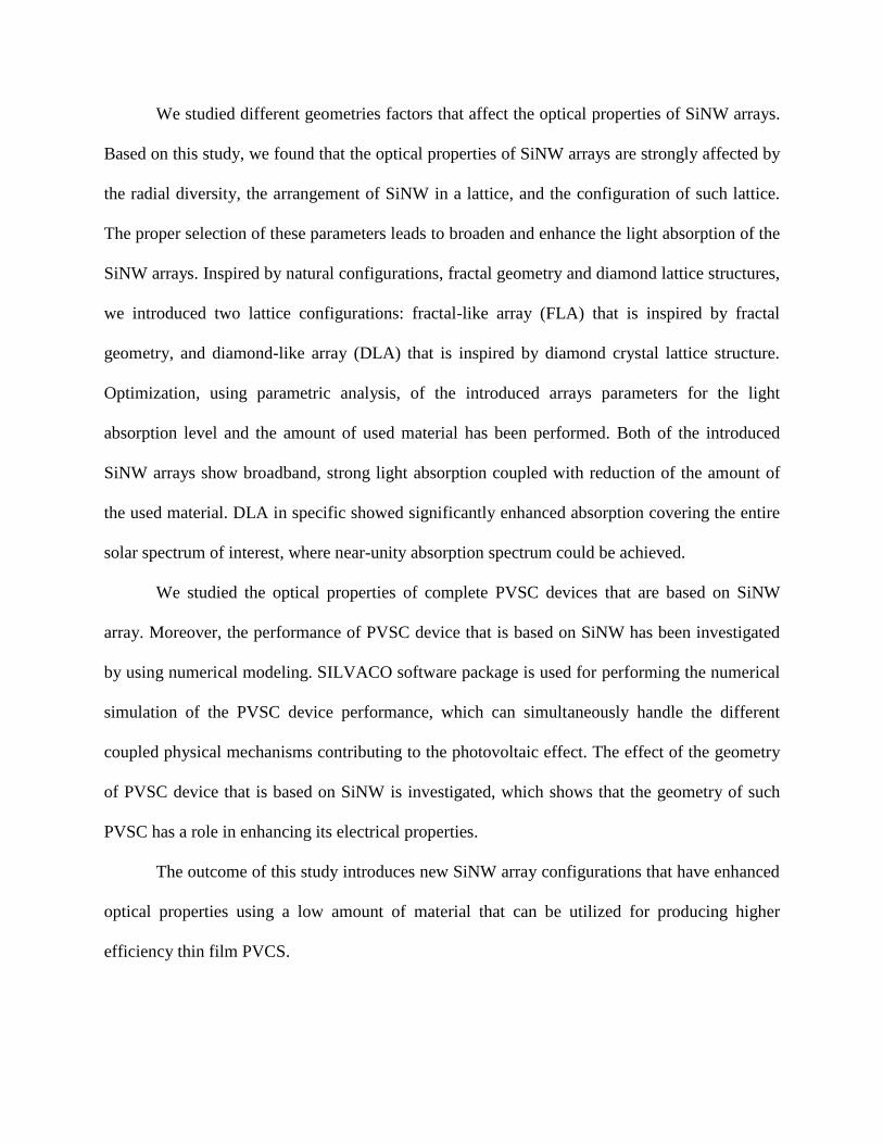
microcontact printing. Figure 1.4 demonstrates the concept the of microcontact technique that is
used to transfer patterns on the top of a substrate. In this technique, the raised surface of a
template contacts an ink pad, then contacts the substrate to transfer the ink material with the
template (mold) pattern [29]. The transferred pattern can be used later to grow the SiNW arrays
using the VLS technique that is demonstrated in Fig. 1.1.
8
Fig. 1.4. Schematic of microcontact printing to transfer patterns from PDMS molds onto
substrate. Taken from [29].
1.3 Organization of this Dissertation
This dissertation has a focus on enhancing the efficiency of (SiNW) arrays for thin film solar
cells applications, and the viability of solar cell based on the SiNW. Based on this the
dissertation is organized as follows: Chapter 1 has given an introduction to the study of SiNW
arrays and the motivation of our research works on the optical properties of the SINW arrays.
Chapter 2 provides a literature review of the fundamental concepts underlying this thesis, such
as, silicon optical properties, factors that affect SiNW arrays optical properties, and models of
the optical properties of SiNW arrays. In addition, the methodology of the dissertation wok is
included in this chapter. Chapter 3 describes the effect of the diversity of the geometrical
parameters of an array, mainly the radial diversity, and the arrangement of the NW with radial
diversity on the absorption spectrum of SiNW arrays. This chapter introduces the basics for
SiNW array design that will be used the next chapters. Chapter 4 introduces new diverse SiNW
array configurations inspired by fractal geometry. Design principles of such arrays with
numerical analyses of their optical properties are included. Chapter 5 is dedicated to the study of
another new SiNW array configuration, inspired from the diamond crystal lattice structure. In
addition, this chapter introduces silicon nano-cone (SiNC) arrays are studied in this chapter.
Chapter 6 presents the optical properties of PVSC that based on the SiNW arrays. Moreover, the
electrical properties of PVSC devices that are based on SiNW and SiNC are investigated, with

9
emphasis on the role of NW and NC geometry in enhancing the electrical performance of such
device. Finally, Summary conclusions and future works are included in Chapter 7.

10
CHAPTER 2
SiNW Arrays Optical Properties and Models
Silicon is a widely used material in the current electronic devices industry and has been heavily
studied by the scientific community. Therefore, its chemical and physical properties are well
known and published. Silicon is indirect band gap material that interacts with and weakly
absorbs photons. However, silicon is widely used in commercial PVSC due to many factors,
such as: it is abundant, nontoxic, processable, and has near-ideal band gap for solar cell
applications. Since the optical properties of silicon have a key role in silicon based PVSC
performance, we have presented these properties in this chapter. SiNW arrays show unique
optical properties relative to equivalent-thickness flat silicon films, which makes producing high
efficiency thin film PVSC very promising. To date, the lower efficiencies of nanowire-based
solar cells have outweighed their benefits [9]. For this reason, better understanding of the optical
and electrical properties of the NW arrays, and the factors that affect these properties is
important to fully utilize them for electro-optical applications. In this chapter, we present the
factors that affect the optical properties of NW arrays, and some popular approximate models of
the NW arrays optical properties that have been proposed in the literature. Numerical modeling
approach, which is adopted in our study of the optical properties of SiNW arrays, is also
explained in this chapter.
2.1. Optical Properties of Silicon
Crystalline Silicon (cSi) is a dispersive material; its index of refraction as a function of the
wavelength in the optical band as shown in Fig. 2.1. The index of refraction for silicon is a

11
complex numbers as �� = � − �� , where � is the extinction coefficient, and n is the refractive
index.
Fig. 2.1 The Real and imaginary parts of the complex refractive index for silicon at 300 K [30].
The absorption coefficient(�) and the reflectance (R) of a material can be calculated from the
index of refraction as:
� =�
� (2.1)
=(���)����
(���)���� (2.2)
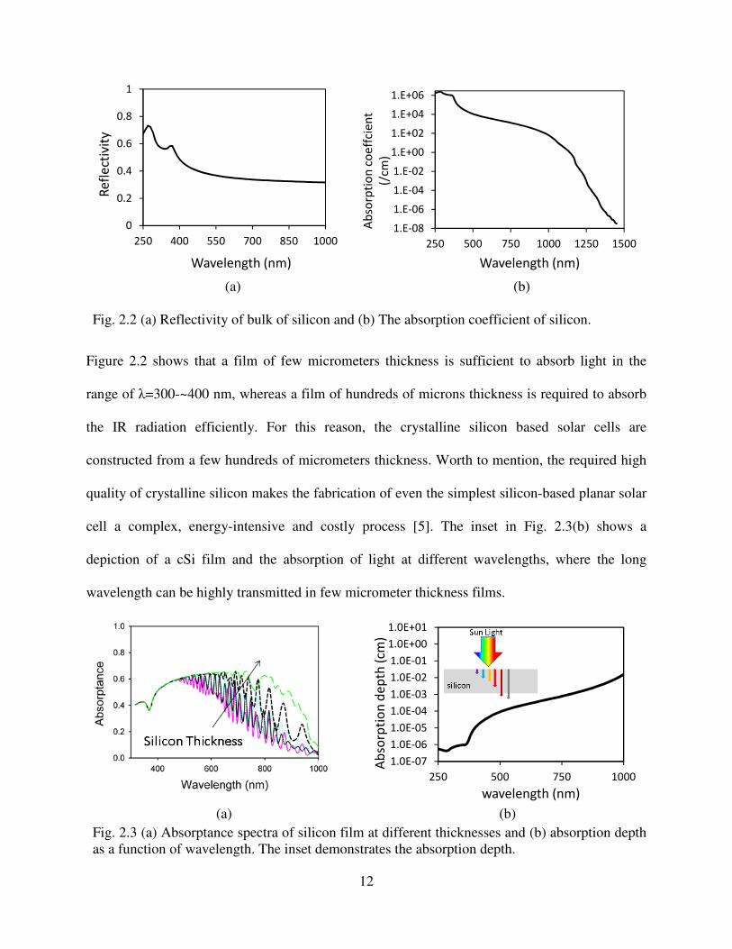
where λ is the free space wavelength. The reflectance and the absorption coefficient of the bulk
cSi are shown in Fig. 2.2 (a, b). High reflectance is observed over the entire band, especially at
the range of λ=~300-~400 nm. The low absorption coefficient (α) in the range of λ= 400- 1000
nm is shown in Fig. 2.2(b), which shows one of the silicon optical disadvantages as a weak
absorber. The low absorption coefficient means that a thickness in the order of 100 µm is
required to absorb the near IR radiation. Figure 2.3(b) demonstrates this concept and points out
the required amount of material to efficiently absorb light at different wavelengths of the solar
spectrum.
0
1
2
3
4
5
6
7
300 400 500 600 700 800 900 1000
n,
-k
Wavelength (nm)
Index of refraction(n)
Extenction Coeffeceint(k)
12
(a) (b)
Fig. 2.2 (a) Reflectivity of bulk of silicon and (b) The absorption coefficient of silicon.
Figure 2.2 shows that a film of few micrometers thickness is sufficient to absorb light in the
range of λ=300-~400 nm, whereas a film of hundreds of microns thickness is required to absorb
the IR radiation efficiently. For this reason, the crystalline silicon based solar cells are
constructed from a few hundreds of micrometers thickness. Worth to mention, the required high
quality of crystalline silicon makes the fabrication of even the simplest silicon-based planar solar
cell a complex, energy-intensive and costly process [5]. The inset in Fig. 2.3(b) shows a
depiction of a cSi film and the absorption of light at different wavelengths, where the long
wavelength can be highly transmitted in few micrometer thickness films.
(a) (b)
Fig. 2.3 (a) Absorptance spectra of silicon film at different thicknesses and (b) absorption depth
as a function of wavelength. The inset demonstrates the absorption depth.
0
0.2
0.4
0.6
0.8
1
250 400 550 700 850 1000
Re
fle
ctiv
ity
Wavelength (nm)
1.E-08
1.E-06
1.E-04
1.E-02
1.E+00
1.E+02
1.E+04
1.E+06
250 500 750 1000 1250 1500
Ab
sorp
tio
n c
oe
ffci
en
t
(/cm
)
Wavelength (nm)
1.0E-07
1.0E-06
1.0E-05
1.0E-04
1.0E-03
1.0E-02
1.0E-01
1.0E+00
1.0E+01
250 500 750 1000
Ab
sorp
tio
n d
ep
th (
cm)
wavelength (nm)
13
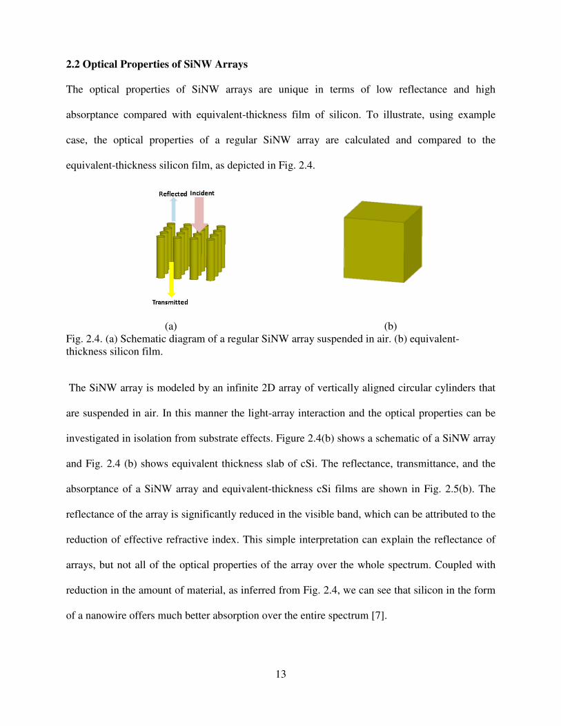
2.2 Optical Properties of SiNW Arrays
The optical properties of SiNW arrays are unique in terms of low reflectance and high
absorptance compared with equivalent-thickness film of silicon. To illustrate, using example
case, the optical properties of a regular SiNW array are calculated and compared to the
equivalent-thickness silicon film, as depicted in Fig. 2.4.
(a)
(b)
Fig. 2.4. (a) Schematic diagram of a regular SiNW array suspended in air. (b) equivalent-
thickness silicon film.
The SiNW array is modeled by an infinite 2D array of vertically aligned circular cylinders that
are suspended in air. In this manner the light-array interaction and the optical properties can be
investigated in isolation from substrate effects. Figure 2.4(b) shows a schematic of a SiNW array
and Fig. 2.4 (b) shows equivalent thickness slab of cSi. The reflectance, transmittance, and the
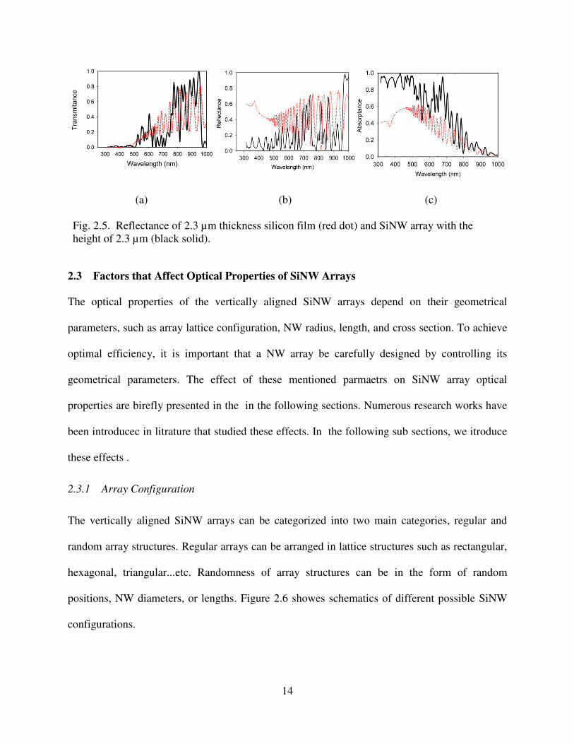
absorptance of a SiNW array and equivalent-thickness cSi films are shown in Fig. 2.5(b). The
reflectance of the array is significantly reduced in the visible band, which can be attributed to the
reduction of effective refractive index. This simple interpretation can explain the reflectance of
arrays, but not all of the optical properties of the array over the whole spectrum. Coupled with
reduction in the amount of material, as inferred from Fig. 2.4, we can see that silicon in the form
of a nanowire offers much better absorption over the entire spectrum [7].
14
(a) (b) (c)
Fig. 2.5. Reflectance of 2.3 µm thickness silicon film (red dot) and SiNW array with the
height of 2.3 µm (black solid).
2.3 Factors that Affect Optical Properties of SiNW Arrays
The optical properties of the vertically aligned SiNW arrays depend on their geometrical
parameters, such as array lattice configuration, NW radius, length, and cross section. To achieve
optimal efficiency, it is important that a NW array be carefully designed by controlling its
geometrical parameters. The effect of these mentioned parmaetrs on SiNW array optical
properties are birefly presented in the in the following sections. Numerous research works have
been introducec in litrature that studied these effects. In the following sub sections, we itroduce
these effects .
2.3.1 Array Configuration
The vertically aligned SiNW arrays can be categorized into two main categories, regular and
random array structures. Regular arrays can be arranged in lattice structures such as rectangular,
hexagonal, triangular...etc. Randomness of array structures can be in the form of random
positions, NW diameters, or lengths. Figure 2.6 showes schematics of different possible SiNW
configurations.
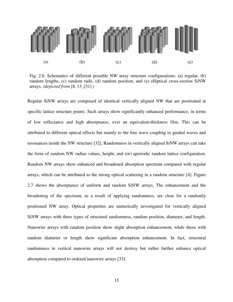
15
(a) (b) (c) (d) (e)
Fig. 2.6. Schematics of different possible NW array structure configurations: (a) regular, (b)
random lengths, (c) random radii, (d) random position, and (e) elliptical cross-section SiNW
arrays. (depicted from [8, 13 ,[31] )
Regular SiNW arrays are composed of identical vertically aligned NW that are positioned at
specific lattice structure points. Such arrays show significantly enhanced performance, in terms
of low reflectance and high absorptance, over an equivalent-thickness film. This can be
attributed to different optical effects but mainly to the free wave coupling to guided waves and
resonances inside the NW structure [32]. Randomness in vertically aligned SiNW arrays can take
the form of random NW radius values, height, and (or) aperiodic random lattice configuration.
Random NW arrays show enhanced and broadened absorption spectrum compared with regular
arrays, which can be attributed to the strong optical scattering in a random structure [4]. Figure
2.7 shows the absorptance of uniform and random SiNW arrays. The enhancement and the
broadening of the spectrum, as a result of applying randomness, are clear for a randomly
positioned NW array. Optical properties are numerically investigated for vertically aligned
SiNW arrays with three types of structural randomness, random position, diameter, and length.
Nanowire arrays with random position show slight absorption enhancement, while those with
random diameter or length show significant absorption enhancement. In fact, structural
randomness in vertical nanowire arrays will not destroy but rather further enhance optical
absorption compared to ordered nanowire arrays [33]

16
(a) (b)
Fig. 2.7. Absorptance spectra of different SiNW arrays: (a) Absorptance of ordered and random
silicon NW arrays, (b) Absorptance spectra for periodic and optimal aperiodic SiNW arrays. (
Taken from [13] and [33] ).
2.3.2 Lattice Constant of Uniform Nanowire Arrays
Lin et al. [34] have studied the effect of the lattice constant on the optical properties of uniform
SiNW arrays with constant filling fraction. In that work, it has been shown that changing the
lattice constant has impact on the optical of the array. For clarity and to isolate other factors than
lattice constant, we show a case study for two uniform SiNW arrays with constant radius value
and length, and variable lattice constant. The effect of changing lattice constant of the two
uniform NW arrays on their absorption spectra is shown in Fig. 2.8. We can see that in the case
of the NW radius of 50 nm, as the lattice constant increases the position of the absorption peaks
red-shifts slightly. The same applies for the case of the 30 nm NW radius. At a constant values of
SiNW array length and radius, the lattice constant of the array has minor effect on the absorption
peak position. Even though, the magnitude of the absorption peaks is degraded as the lattice
constant increases

17
(a)
(b)
Fig. 2.8. Absorptance spectra of a regular SiNW array calculated at different lattice constants, a,
with height of 2.3 µm. Two SiNW arrays are tested with radius values of: (a) R= 50 nm and (b) R
= 30 nm.
2.3.3 Nanowire Radius Effect
The effect of radius of the NW radius on NW array absorption spectrum has been explored by
numerous studies analytically [15, 35, 36] experimentally [37], and numerically [32, 38]. For
example, Yu et al. [36] have analytically studied single NW and the effect of its radius on its
optical properties. Chu et al. [38] presented one of the first numerical studies about the SiNW
arrays, where they showed the effect of different parameters including the radius value of a NW.
Sturmberg et al. [32] studied NW arrays analytically and numerically, where they show that the
radius effect on NW arrays optical properties. Khorasaninejad et al. [37], experimentally,
measured the optical properties of different uniform SiNW arrays with different radius values,
were they showed the direct impact of NW radius on the optical properties. In an array composed
of circular cylinder NW, radius has a major effect on the absorption spectrum, as the radius
increases the peak’s position red shifts. For this reason, the SiNW radius value is considered a
key element in determining the absorption spectrum of a SiNW array.

18
This phenomenon is utilized in our research for designing broadband absorption SiNW arrays.
Figure 2.9 shows the absorption spectra of regular arrays composed of SiNW of different radius
values. The NW radial value effect on the absorption spectrum can be seen in as red shift of the
absorption peak as the radius increases.
(a) (b)
Fig. 2.9. (a) 3D depiction of a uniform periodic SiNW array, and top view of the unit cell. (b)
Absorption spectra of uniform periodic SiNW arrays, with fixed lattice constant and height
(h) at different radius values(R). The absorption peaks that corresponds to each radius value
are shown, where the red shift as the radius increases is shown.
2.3.4 Nanowires Length Effect
The practical height of a SiNW arrays is typically in the order of few microns [39]. Huang et al.
[9] studied the effect of the length of NW arrays on light absorption, where they showed the
superiority of the NW array compared with flat film of counterpart material. Figure 2.10 shows
the performance of SiNW array and thin cSi film represented by the ultimate efficiency, as
defined in Section (2.5), vs height. This advantage of the SiNW array can be seen from two
aspects: material savings and efficiency enhancement. For example, to achieve 20 % ultimate
efficiency, we can use 1000 nm height SiNW array, whereas 10000 nm thickness films is
19
required to achieve the same efficiency, as inferred from Fig. 2.10. This means reducing of the
amount of used material by at least 90% of the film material. Reducing the amount of the used
material and enhancing the efficiency of PVSC are main goals of research community that would
lead to the high efficacy low cost thin film PVSC. The material saving (gain), as well as the
ultimate efficiency and filling fraction of the material, can be considered as figure of merits of
SiNW arrays performance.
Fig. 2.10. Regular SiNW array and equivalent-thickness cSi film ultimate efficiencies as a
function of the height (length). Taken from [9].
2.3.5 Lattice Configuration of NW Array Effect
The effect of lattice configuration on the absorption spectrum of an array has been studied in the
literature [40]. In the following example we show two arrays that have the same lattice constant,
a = 600 nm, and NW radius R =180 nm, but with different lattice configurations, rectangular and
hexagonal. Figure 2.11(a, b) shows the lattice configurations and the absorption spectra of the
two arrays. We can see that both yield absorption spectra with almost the same trend in the entire
solar spectrum with minor differences, mainly in the IR band. Lattice configuration has minor
effect on the absorption spectrum of uniform arrays [40]. This can be attributed to the fact that

20
the lattice configuration, while keeping all other parameters as constant, does not affect the
surrounding space around the NW. Which means that the wave coupling conditions between are
not changed, hence the propagation mechanism of light in the array structure are not largely
affected.
(a) (b)
Fig. 2.11. (a) 3D depiction of hexagonal and rectangular SiNW arrays , (b) Absortion spectra of
the hexagonal(black doted line, and the rectangular SiNW arrays(red solid line). The lattice
constant, radius and the hieghtof the arrays are 600 nm , 180 nm , and 2.3 µm, respectively [40].
2.4 Models of Optical Properties of Nanowire Array
In classical solar cells, the physical dimensions are much larger than the light wavelengths,
where geometrical ray optics model is used to study their optical properties giving excellent
accuracy. For objects with feature sizes near the wavelength, as the case in the NW arrays, the
geometrical optics becomes not valid for modeling the optical properties due to the different
optical effect that can appear at these feature size dimensions. Therefore, Different models have
been proposed to explain and predict the optical properties of SiNW arrays [6]. Because light
interaction with arrays shows different complex optical effects, a comprehensive model that can
explain the optical properties of the different configurations of NW arrays over the entire solar
21
spectrum is currently impossible[41]. However, different analytical models have been suggested
in literature to explain the optical properties of semiconductor NW, such as effective medium
theories (EMT), optical wave guide, leaky mode resonance, DRA, and scattering models [3]-[6],
[4,10], [42]–[46]. Each of these models invokes some assumptions and neglects some effects that
makes them valid for predicting and explaining optical properties in special cases, but cannot be
generalized to all the configurations of NW arrays over the entire spectrum.
2.4.1 Effective Medium Theories
Effective medium theories (EMTs) are used to calculate the effective properties of a medium
with inclusions, and based on the properties of individual components and their fractions in a
composite. The main property that is calculated using EMTs is the effective dielectric constant,
from which the effective refractive index can be calculated [41]. Two of these- Maxwell-
Garnet(MG) and Bruggeman approximations have been considered in literature for explaining
the optical properties of NW arrays [6, 41]. However, neither the MG nor the Bruggeman
approximation considers the wave coupling between the neighbor nanowires. Hu et al. show that
the GM model underestimates the absorption of the SiNW array and the obtained results do not
agree with simulations or experimental results [38].
2.4.2 Optical Waveguide Model and Leaky Mode Resonances
Optical waveguides are dielectric waveguides composed of a dielectric material with high index
of refraction surrounded by a material with a lower index of refraction [47]. This definition
applies to SiNW, which could be considered as dielectric waveguides that support guided waves
propagation. By applying the optical waveguide model to the SiNW arrays, Sturmberg et al
showed that the absorption peak positions are dependent on the radius [32]. Such position peaks

22
corresponds to resonance modes of a dielectric waveguide, which can be found by solving the
characteristic equation of dielectric wave guide that is given as [48, 49]:
( )( )
( )( )
( ) ( )( )
( ) ( )( )
2 2 2' ' ' '2 20 0
2 2 2
1 1 in outJ R K R n k J R n k K R
J R K RR J R K R
+ + × +
= ν ν ν ν
ν ν ν ν
κ γ κ γβ ν
κ γ κ κ γ γ κ κ γ γ (2.3)
where κ and γ are the transvers wave vectors inside and outside the NW, Jν and Kν
are
Bessel functions of the first and second kinds, β is the wave vector along the NW axis, R is the
NW radius, ν is the order of the Bessel function, inn is the core refractive index, and out
n is the
outside martial refractive index. Analyses of the dielectric wave guide and the resonance modes
are provided in Appendix (A). This model can explain and predict absorption peaks of a single
NW with high accuracy. However, it does not take into consideration the mutual wave coupling
in nanowires in the case of an array. Such mutual wave coupling has impact on the array optical
properties and cannot be neglected, especially in dense NW arrays. To take wave coupling
between NW in consideration, Fountain et al [35], based on Sturmberg et al. work [32],
introduced a modified eigenvalue equation for infinite NW arrays as:
( )( )
( ) ( )( ) ( )
( ) ( )( )
( ) ( ) ( )( ) ( )
2 ' ' '2 20
2 2 2
0
2 2' ' '
0 0 0
0
1 1
in out
J R R S J R
J R H R S J R
n k J R n k H R S J R
J R H R
H
R
S J R
+ ± + = − +
+× − +
ν ν ν
ν ν ν
ν ν ν
ν ν ν
κ γ γβ ν
κ γ κ κ γ γ γ
κ γ γ
κ κ γ γ γ
2.4)
where Hν is the Hankel function of the thν order, and 0S represents the nearest neighbor
interaction within the lattice[35]. The leaky mode resonance model explains the strong
absorption peaks of the NW arrays by the coupling of free space plane wave into radial leaky
waveguide modes, which are electromagnetic modes with enhanced electric and magnetic field
23
intensities localized inside the nanowire [50]. This model invokes the assumption of infinite
length and lossless material of the optical wave guide, where the losses and the finite length of
the NW are not considered.
2.4.3 Scattering: Mie Scattering Model
Mie solution introduced the theory of electromagnetic plane wave scattering by
a dielectric sphere, and later applied to infinite length cylinders, with a radius in the order of the
scattered wavelength [51, 52]. This scattering effect is suggested to explain the optical properties
of SiNW arrays, especially for diluted SiNW arrays [45]. Since SiNW in an array have
dimensions in the order of the wavelength, Mie solution is suggested to model the optical
properties of NW arrays. Mie solution is suitable for modeling infinite length single NW, and
can be used as an approximation model for single NW or diluted NW arrays, since the mutual
effect between NW is negligible. For dense SiNW arrays, Mie scattering approach does not
consider mutual coupling effects, which renders it inaccurate [53].
2.4.4 Dielectric Resonance Antenna and Fabry-Perot Models
The dielectric resonator antenna (DRA) model has been suggested in the literature to explain the
peaks in the absorption spectrum of SiNW such as in Ref. [54] and [37]. This model considers
SiNW to behaves as a dielectric resonator antenna (DRA) that can support resonance modes
under excitation [43]. The Fabry-Perot model, in its simple form, can be produced by a material
with two parallel interfaces. Due to the finite length of SiNW, Fabry–Pérot-like behavior can be
adopted to explain the absorption peaks in the NW arrays’ absorption spectra [37]. In this model,
the enhanced absorption and the absorption peaks are attributed to the resonance modes of the
array which behaves like a Fabry-Perot resonator. Both of these models consider individual
SiNW neglecting the coupling effect of the adjacent wires. However they succeed in explaining
24
peaks of single NW absorption spectra. Zeng et el proposed the DRA analytical model to predict
absorption peaks in a SiNW array, where SiNW is considered as a circular cylinder that
resonates under light excitation with resonance modes [43]. An approximation analytical formula
for determining the resonance frequencies for the lowest resonance mode is given as [43, 55]:
21 6.324
0.27 0.36 0.022 2
si
R R
h hRλ π ε
= + +
+ (2.5)
Where si
ε is the silicon relative permittivity, λ the free space wavelength, and R and h are the
radius and the height of the NW. This closed from approximation predicts only the lowest order
fundamental mode resonance frequency, and originally derived for DRA antenna in the
microwave applications [22]. This model, as other models, is a valid approximation for single
SiNW and neglects the coupling effects between NW in an array. Another important fact is that
this model assumes low losses in the DRA material, which makes it suitable for modeling the
SiNW optical properties in the IR band where the absorption of silicon is weak.
2.5 Numerical Modeling of SiNW Arrays
As mentioned earlier, light interaction with SiNW arrays encompasses different optical effects;
therefore it is difficult to have an analytical model that considers all of optical effects and can
predicts array’s optical properties with reasonable accuracy. Consequently, numerical simulation
becomes inevitable to model the optical properties of SiNW arrays. The light-NW arrays
interaction can be simulated by using different electromagnetics computational methods such as
the finite element method (FEM)[57], the finite different time domain (FDTD)[13, 58], and
transfer matrix method (TMM)[38]. In this work, we adopt electromagnetic FEM numerical
solver employed by Ansys HFSS software package. HFSS, equipped with a CAD interface,
allows the user to design complex 3-D structure with subwavelength dimensions, and can

25
employ experimental optical properties of materials. All of these, especially implementing
experimental optical properties of materials in the computations, render the simulation results
physically realistic. Worth mentioning is that using the optical properties of bulk silicon are
implemented, because the NW dimensions in this study are far larger than the dimensions at
which that quantum effects on the optical properties of material can occur. In order to focus on
studying the physics of the light-NW arrays interaction in isolation from other effects, the array
is assumed to be surrounded by air, as shown schematically in Fig. 2.12(a). In this manner, a
SiNW array is considered as infinite 2D array in the X and Y directions with a finite length in the
Z direction. The SiNW array consists of nanowires of radius (R), and height (h), arranged in a
lattice with a constant (a), as in Fig 2.12. These three geometrical parameters will be under focus
of our analyses in this work. To realize the array in the simulation domain, we employ a periodic
unit cell by using the perfect electric conductor (PEC) and perfect magnetic conductor (PMC)
walls. By this manner, an infinite array is modeled by limited space unit cell in the simulation
domain. Fig. 2.13(c) below gives idea of how an infinite SiNW arrays is realized in the
simulation domain.
(a) (b) (c)
Fig. 2.12. Schematic of the SiNW array: (a) 3D depiction of SiNW array, (b) Top of the array,
(c) top view of the unit cell showing the periodic boundary conditions, where perfect electric
conductor (PEC) and perfect magnetic conductor (PMC) walls are employed.
PM
C
PEC
PEC
PM
C h
a
R

26
A depiction of the unit cell in the simulation domain with the suitable boundary is shown in Fig
2.13, where the PEC and PMC walls are demonstrated. Perfectly matched layers (PML) are
added at the top and bottom of the unit cell simulation domain to mimic infinite space.
Fig. 2.13. The simulation domain of the periodic unit cell of the NW array with the boundary
conditions that are used to realize the infinite NW array.
To quantify the performance of the cSi film and the SiNW arrays, the ultimate efficiency is used
as:
300
4000
300
( ) ( )
( )
g
nm
nm
nm
I A dg
I d
∫
=
∫
λ λλ λ λ
λη
λ λ (2.6)
where λ is the wavelength in nm, �� is the wavelength corresponding to the crystalline silicon
band gap, I(λ) is the standard AM1.5 solar spectrum, and A(λ) is the absorptance. The ultimate
efficiency implies assumptions that each photon absorbed with higher energy than the band gap

27
energy is converted into one carrier pair and is collected without considering material losses.
Figure 2.14 shows the standard air mass 1.5 (AM1.5) solar irradiance spectrum, where the sub
band that can be utilized by crystalline silicon is shaded by yellow. The AM1.5 represents the
length of the sun light path through the atmosphere, where the shortest path is when the sun is
directly over the head is designated as AM1.0. The AM can defined as the ratio of the actual
path length to the shortest path length of the sun light when passes through atmosphere [59].
Fig. 2.14. AM1.5 solar irradiance spectrum and the usable band of the spectrum by crystalline
silicon for PVSC applications [60].
Normal plane wave with parallel polarization is assumed to illuminate the arrays in our study of
the arrays optical properties. The band of interest covers the range of λ= 315- ~1100 nm and the
absorptance of an array is calculated as:
A(λ)=1-R(λ)-T(λ) (2.7)
where R(λ) and T(λ) are the wave length dependent reflectance and transmittance of the array
respectively. To calculate the reflectance and transmittance, we employ the scattering matrix
method, as shown in Appendix (B).

28
Summary
Three main ideas are discussed in this chapter: (i) the crystalline silicon and the SiNW arrays
optical properties, (ii) Models that are used for NW arrays optical properties, and (iii) numerical
modeling of the NW array that we use in our research. SiNW arrays have superior performance
over the equivalent-thickness slab of silicon material. To explain this, different approximation
models have been proposed in the literature. These models are discussed briefly in this chapter,
showing their advantages and disadvantages. The optical effect in SiNW arrays comprises of
multiple physical mechanisms and optical effect that govern the total optical properties of the
NW arrays. There is no global analytical model, so far, that can explain the optical properties of
SiNW arrays over the entire spectrum of interest. For this reason, numerical modeling and
simulation have been adopted in the literature, as well this dissertation, for conducting research
about the optical properties of NW arrays.

29
CHAPTER 3
Radial Diversity in SiNW Arrays
The Properly designed NW arrays have lower reflectance, higher absorptance, and use less
amount of material in comparison with counterpart equivalent-thickness flat film. The optical
properties of vertically aligned NW arrays can be tuned and controlled by adjusting their
geometric parameters such as NW height, radius, cross section, and array lattice constant [4, 6].
Numerous researchers have proposed different array configurations to enhance the SiNW arrays’
absorption spectrum[4]–[6]. One of parameter that has large effect and can be used for tuning the
optical properties of SiNW arrays is the radius value of NW [61]. In this chapter, we study the
effect of geometrical diversity, especially radial diversity of nanowires, on the optical properties
of the SiNW arrays. In addition, the effect of lattice configurations and the arrangement of the
diverse radii NW in certain lattice configurations is also studied. Two concepts are introduced in
this chapter, the limited and broad diversity of radii of arrays. To this end, three types of SiNW
array configurations are studied (i) uniform periodic arrays (ii) modified periodic NW arrays that
include diversity of radii (iii) modified NW arrays including radii diversity with different NW
arrangements in the unit cell. This chapter is dedicated to demonstrate and study the role of
radial diversity, the lattice configuration, and the arrangement of NW on the absorption spectrum
of a SiNW array.
3.1 Uniform periodic arrays
In order to show the effect of radius of NW on the absorption spectrum of an array, we first study
a uniform periodic array with fixed height (h) and lattice constant (a). The absorption spectrum
of a uniform SiNW array with fixed height and lattice constant has peak positions that depend on
the NW radius. This dependency can be explained by the characteristic equation of a dielectric

30
wave guide as demonstrated in Chapter 2. As an example, the absorption spectrum of a diluted
uniform rectangular array with fixed lattice constant (a=400 nm) and height (h=2.3 µm) is
calculated at different radius values. Figure 3.1(b) shows the peaks of absorption spectra
positions that depend on the radius value of the SiNW. The red-shift of the peak position as the
NW radius increases is quite clear in this example.
(a) (b)
Fig. 3.1. (a) 3D depiction of a uniform periodic SiNW array, and top view of unit cell. (b)
Absorption spectra of uniform periodic SiNW arrays, with fixed lattice constant and height (h)
at different radius values(R). The absorption peaks that corresponds to each radius value are
shown, where the red shift as the radius increases is shown.
Conceptually, the simplest extension of the electromagnetic principles observed in the uniform
nanowire arrays to achieve broadband absorption is to introduce multiple and diverse nanowire
radii in a single periodic unit cell. By proper design and NW radii selection, the absorption
spectrum can have multiple overlapping absorption peaks. In order to increase the number of
peaks, we propose broadening of the diversity of NW radius values. In other words, as the
number of different NW radii values increases in a unit cell, the number of absorption peaks
h
a
a
R

31
increases and consequently the spectrum broadens and is enhanced. This leads us to introduce
the concepts of limited and broad diversity of NW radii values in SiNW array designs. These two
concepts are investigated in this chapter by illustrative example, and will be utilized in Chapters
4 and 5.
3.2 Modified periodic arrays
In order to study the effect of radial diversity of NW on the absorption spectrum, a uniform
periodic array is modified firstly to include two different NW radius values in a periodic unit
cell. This configuration represents what we have termed as limited diversity. Secondly, to show
the effect of broadening the diversity of the NW radius values, the uniform periodic SiNW array
is modified to two different arrays: One includes three different radius value NW, while the other
includes four different radius value NW. In these four SiNW array examples, the height and the
lattice constant are kept constant. The arrangement of the NW in a unit cell is kept simple, where
the positioning of the NW follows descending order as shown in Fig.3.2. The NW are color
coded based on their radius values. The NW radius values and the lattice constant are selected in
a manner to illustrate the effects. Four different radius values are selected, 60 nm (green), 50 nm
(red), 40 nm (blue), and 30 nm (cyan) as shown in Fig. 3.2.
(a) (b) (c) (d)
Fig. 3.2. The four different arrays: (a) uniform array , (b) modified array with two radius
values, (c) three radius values, and (e) four radius values NW.

32
Figure 3.3 demonstrates the concept of multi peaks generation in an absorption spectrum by
using multi NW radius values. The absorption spectrum of two uniform arrays is shown in the
dashed lines of Fig. 3.3. The firs array is composed of NW of radius (R=60 nm) with lattice
constant (a=400 nm), and the other array is composed of NW of radius (R=40 nm) with lattice
constant (a=400 nm). The array composed of NW that have two radius values (R1=60 nm, and
R2=40 nm) has absorption spectrum that looks as the superposition of the two spectra of the other
two arrays of single radius value NW.
Fig. 3.3. Absoption Spectrum of limited diversity array composed of two radius vluae
nanowire(solid black), and the spctra of tow uniform peridoc arrys: the first composed of NW
of radius = 60 nm (red dashed) and the other one of NW radius = 40 nm (green dashed).
It is clear that including NW with multi radius values in a periodic unit cell creates an absorption
spectrum with multi absorption peaks which can be seen in Fig 3.4. The effect of broadening the
diversity of radii on absorption spectra is shown by absorption spectra of the arrays in Fig. 3.4.
This behavior of absorption spectrum of the multi radii SiNW arrays can be understood from the
leaky waveguide model as described in Chapter 2 and Appendix (A). The inclusion of different
radii SiNW makes the array structure to support multiple weakly guided resonances that
corresponds to the different absorption peaks. The multi radii NW results in an array structure

33
which can support multiple leaky resonances. The ultimate efficiency and the volume filling
fraction are calculated and considered for quantifying the performance of the arrays.
(a)
(b)
(c)
(d)
Fig. 3.4. Absoption spectra of four different SiNW arrays: (a) uniform periodic array, and
modified periodic array with(b) two, (c) three, and (d) four nanowires radii. The insets
show 3D depectin of the arrays with color coded NW.
It is worth mentioning that these SiNW arrays are not optimized and are used to illustrate the
effect of diversity on the absorption spectrum. Despite this, the enhancement of the ultimate
efficiency and the filling ratio are quite noticeable as Table 3.1 shows. It can be seen that the
ultimate efficiency is enhanced by including the diversity. In addition, the amount of material,
represented by volume filling fraction, is reduced. One can see the trend of the enhancement in

34
the ultimate efficiency and reduction of the amount of used material as the diversity of the NW
radii is broadened from two radius values to four radius values. The obtained results in this
section lead us to propose the broad diversity concept as will be discussed in the following
Section (3.5). A very interesting observation from Table 3.1 is that a SiNW array of filling
fraction of 4.2% can achieve almost the ultimate efficiency of the equivalent-thickness flat film.
This result means that ~ 95% saving in the martial is achieved.
Table 3.1- Ultimate efficiency and filling fraction of the different SiNW arrays
Uniform array
Diverse radius arrays
Two radii Three radii Four radii
Ultimate Efficiency 10.3% 10.6% 12.5% 13.5%
Filling Fraction 7.0% 5.1% 5.0% 4.2%
3.3 Effect of Lattice structure and distribution of the diverse NW
To test the effect of lattice configuration and the arrangement of the diverse radii NW in these
lattice configurations, two lattice configurations are slected, rectangular and hexagonal. First, we
test the effect of different lattice configuration on the absoption spectrum, later we test the
arrangment of diverse radius NW in a lattice configuratio.
3.3.1 Lattice Configuration Effect
Lattice configuration in the case of uniform NW arrays has minor effect on their performance in
terms of absorption spectrum and ultimate efficiency as shown in the previous chapter. This is
demonstrated by example given in Fig. 2.11 in the previous chapter. To study the effect of the
lattice configuration of diverse radii NW array, two lattice configurations are considered:
rectangular and hexagonal as shown in Fig. 3.5. In these two lattice configurations, the same

35
values of the NW radii are employed, with the same color coded values as in the previous
section. Lattice constant and height are kept the same in both of the configurations. The NW
radius values 60, 50, 40, and 30 nm for are R1, R2, R3 and R4 respectively, with lattice as a= 400
nm.
(a) (b)
Fig. 3.5. Diverse SiNW arrays composed of four different NW radii arranged in two
different lattice configurations. (a) Rectangular, and (b) hexagonal lattice structures.
The absoption spectra of these two SiNW arrays are shown in Fig. 3.6. We observe that the
lattice configuration has noticeable impact on the absorption spectrum of diverse arrays, as
inferred from Fig. 3.6. This result has signifcant importance. It raises the question of optimal
lattice structure, and will be used for designing more efficicnt diverse radii arrays in later
chapters.
(a) (b)
Fig. 3.6. Absorption spectra of diverse SiW arrays for two different distributions: (a)
rectangular lattice structure (b) Hexagonal lattice structure. Insets show 3D depiction and
top view of the arrays.
0
0.1
0.2
0.3
0.4
0.5
0.6
0.7
0.8
0.9
1
300 400 500 600 700 800 900 1000
Ab
sorp
tance
Wavelength (nm)
0
0.1
0.2
0.3
0.4
0.5
0.6
0.7
0.8
0.9
1
300 400 500 600 700 800 900 1000
Ab
sorp
tance
Wavelength (nm)
36
3.3.2 Arrangement Effect of Diverse Radius NW
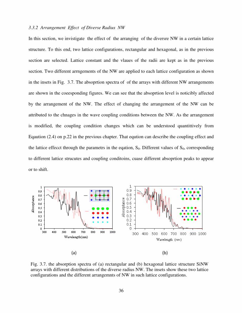
In this section, we invistigate the effect of the arranging of the diversre NW in a certain lattice
structure. To this end, two lattice configurations, rectangular and hexagonal, as in the previous
section are selected. Lattice constant and the vlaues of the radii are kept as in the previous
section. Two different arrngements of the NW are applied to each lattice configuration as shown
in the insets in Fig. 3.7. The absoprtion spectra of of the arrays with different NW arrangements
are shown in the coeesponding figures. We can see that the absoprtion level is noticibly affected
by the arrangement of the NW. The effect of changing the arrangement of the NW can be
attributed to the chnages in the wave coupling conditions between the NW. As the arrangement
is modified, the coupling condition changes which can be understood quantittively from
Eqaution (2.4) on p.22 in the previous chapter. That eqution can describe the coupling effect and
the lattice effecct through the parametrs in the eqation, S0. Different values of S0, corresponding
to different lattice strucutes and coupling conditoins, cuase different absoprtion peaks to appear
or to shift.
(a) (b)
Fig. 3.7. the absorption spectra of (a) rectangular and (b) hexagonal lattice structure SiNW
arrays with different distributions of the diverse radius NW. The insets show these two lattice
configurations and the different arrangemnts of NW in such lattice configurations.

37
In the rectangular array, we can see the absorption level in the visible band is dramatically
affected by the arrangement of the NW in the elattice. For this particular example, the absoprtion
spectrum in the range of λ>700 nm is not affected by the arrangement of the NW in both array
configurations. This is due to the fact that the NW with the given radii do not support resonance
modes in the range of λ > 700 nm. This phenomenum raises the question not only about the
optimal lattice configuration but also about the optimal arrangemnt of the diverse NW for best
absrption perfromnace. We conclude that arrangement of the diverse radii NW in a certain
lattice has noticeable impact on the absoprtion spectrum, which leads us to think about lattice
configuration with NW arrngement that can enhance and broaden the absoprtion spectrum,
which will be the focus of study in Chapters 4 and 5 in this thesis.
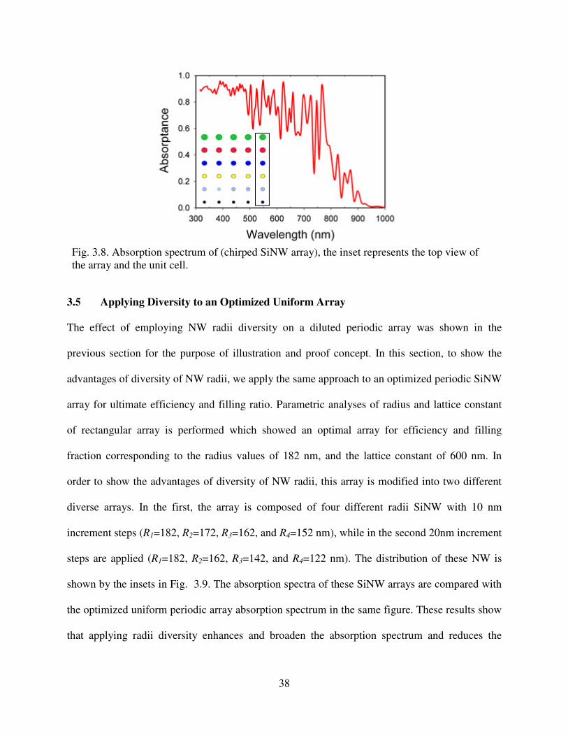
3.4 Effect of Broadening the Diversity of NW Radius Values
In this section, we test the effect of the broadening the range of diversity of the NW radius values
on the array absorption spectrum. It has already been shown in the previous section that as the
range of the radii values broadens; the absorption spectrum is enhanced and broadened. The
current example demonstrates the effect of broadening the range of diversity of the radius values
on the absorption spectrum of a SiNW array. For this purpose, we build an array that is
composed from six different NW radii (40, 50, 60, 70, 80, 90 nm) that are arranged in
rectangular lattice structure as in the inset of Fig. 3.8. The lattice constant is kept as 400 nm and
the arrangement of the NW is made in a form of “chirped” array, as shown by inset in Fig.3.8. It
is obvious that broadening the range of the NW radius values broadens the absorption spectrum
significantly as Fig. 3.8 suggests.
38
Fig. 3.8. Absorption spectrum of (chirped SiNW array), the inset represents the top view of
the array and the unit cell.
3.5 Applying Diversity to an Optimized Uniform Array
The effect of employing NW radii diversity on a diluted periodic array was shown in the
previous section for the purpose of illustration and proof concept. In this section, to show the
advantages of diversity of NW radii, we apply the same approach to an optimized periodic SiNW
array for ultimate efficiency and filling ratio. Parametric analyses of radius and lattice constant
of rectangular array is performed which showed an optimal array for efficiency and filling
fraction corresponding to the radius values of 182 nm, and the lattice constant of 600 nm. In
order to show the advantages of diversity of NW radii, this array is modified into two different
diverse arrays. In the first, the array is composed of four different radii SiNW with 10 nm
increment steps (R1=182, R2=172, R3=162, and R4=152 nm), while in the second 20nm increment
steps are applied (R1=182, R2=162, R3=142, and R4=122 nm). The distribution of these NW is
shown by the insets in Fig. 3.9. The absorption spectra of these SiNW arrays are compared with
the optimized uniform periodic array absorption spectrum in the same figure. These results show
that applying radii diversity enhances and broaden the absorption spectrum and reduces the

39
amount of material relative to the optimized SiNW arrays. The span of the NW radii values
affects the absorption spectrum, and can enhance the array performance.
Fig. 3.9. Absorption spectra for optimized uniform periodic SiNW array, and diverse arrays
(modified optimized uniform periodic arrays). Four different NW radii values are included
in the modified arrays as depicted in the inset.
Quantitatively, the calculated ultimate efficiencies and filling fractions of the three arrays shown
in Fig. 3.9 are shown in Table 3.2. The results show that the diversity in an array enhances the
efficiency of the array and reduce in the amount of the material. This table shows a comparison
of the performance of three arrays in terms efficiency and filling fraction. The enhancement of
the ultimate efficiency and the filling fraction of the modified diverse array over the optimized
uniform arrays are quite clear and significant. The achieved reduction in the amount of material
and the enhancement in the ultimate efficiency are significant relative to equivalent-thickness
silicon film and to optimized uniform arrays. By applying this modification to the regular
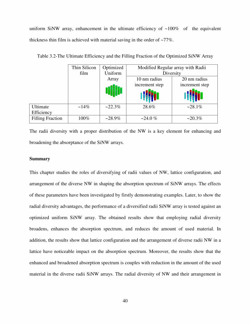
40
uniform SiNW array, enhancement in the ultimate efficiency of ~100% of the equivalent
thickness thin film is achieved with material saving in the order of ~77%.
Table 3.2-The Ultimate Efficiency and the Filling Fraction of the Optimized SiNW Array
Thin Silicon
film
Optimized
Uniform
Array
Modified Regular array with Radii
Diversity
10 nm radius
increment step
20 nm radius
increment step
Ultimate
Efficiency
~14% ~22.3% 28.6% ~28.1%
Filling Fraction 100% ~28.9% ~24.0 % ~20.3%
The radii diversity with a proper distribution of the NW is a key element for enhancing and
broadening the absorptance of the SiNW arrays.
Summary
This chapter studies the roles of diversifying of radii values of NW, lattice configuration, and
arrangement of the diverse NW in shaping the absorption spectrum of SiNW arrays. The effects
of these parameters have been investigated by firstly demonstrating examples. Later, to show the
radial diversity advantages, the performance of a diversified radii SiNW array is tested against an
optimized uniform SiNW array. The obtained results show that employing radial diversity
broadens, enhances the absorption spectrum, and reduces the amount of used material. In
addition, the results show that lattice configuration and the arrangement of diverse radii NW in a
lattice have noticeable impact on the absorption spectrum. Moreover, the results show that the
enhanced and broadened absorption spectrum is couples with reduction in the amount of the used
material in the diverse radii SiNW arrays. The radial diversity of NW and their arrangement in

41
lattice are key element in producing broadband and strong absorption spectrum NW arrays. This
fact leads us to introduce new SiNW array structures that will be discussed in the next chapters.

42
CHAPTER 4
Fractal-Like Silicon Nanowire Arrays
In the previous chapter we demonstrated the role of NW radial diversity and the effect of
their arrangement in enhancing and broadening the absorption spectrum of SiNW arrays. It is
shown that for diverse radius NW, the lattice configuration of an array and the arrangement of
the NW in that array can enhance or degrade performance. This raises a question about the
optimal lattice configuration and arrangement of diverse radii SiNW in such lattice. Since
diverse radii SiNW can be arranged in unlimited number of combinations in different lattice
configurations, we focus in finding a lattice configuration that can offer diversity of geometry.
Fractal geometry has inherent diversity of geometrical parameters, which makes it as a prime
candidate for designing SiNW arrays with geometrical diversity. From a practical perspective, if
metal nanodots are used for creating nanowires in a bottom-up fabrication using slef assembly
them fractal arrangement is a natural possibility. By following the roles of fractal geometry, we
introduce fractal-like SiNW arrays, in the sense of the arrangement and distribution of the NW in
a periodic unit cell. The main goal is to utilize the diversity inherent in fractal geometry to
produce diverse NW arrays with enhanced and broad band absorption spectra. In this chapter, we
first introduce the basic characteristics of fractal geometry. Then, we describe the design of the
fractal-like SiNW arrays, followed by studying their optical properties.
4.1 Fractal geometry
Fractal patterns are not abstract mathematical concept, but they are natural phenomena that can
be found in different aspects of nature such as trees, rivers, mountains, clouds, seashells, etc. A
fractal pattern can be created by having a basic simple and attach a self-similar version of it that
are scaled, translated and rotated iteratively [62]. Qualitatively, a fractal pattern can be defined as

43
a geometric pattern that is divided into infinite number of scaled versions of itself. In other
words, it has symmetry of scale, which means that a part of the main fractal pattern can be
zoomed infinite number of times and it still looks as the main pattern [62, 63]. The smaller self-
similar copies in a fractal pattern are size scaled from the main pattern with a scaling factor, ξ.
The scaling factor, ξ, is defined as the ratio of the size of the main pattern to the size of the
smaller copies from it. We utilize two main properties of the fractal patterns geometry to produce
NW arrays of diversity: the scaling and the translation properties. To demonstrate the concept of
fractal patterns, we give the example of Koch snowflake, famous fractal example [63]. In this
example, an equilateral triangle is the basic geometrical pattern, which is scaled and translated in
the first iteration to generate the shape as in Fig. 4.1. The procedure for creating this fractal
shape is based on three steps: first, draw an equilateral triangle, second, assign the midpoints at
each side in the triangle, and attach size scaled equilateral triangle to the original large triangle as
shown in Fig. 4.1 [63]. Third, continue to repeat step 2 with each scales triangle. At each step,
the triangle should look like these in Fig. 4.1. It is worth mentioning that the procedure that
applies to triangles can be applied to other polygons. In our study, we select the triangle as the
basic pattern because it leads to the hexagonal-like fractal pattern, as Fig 4.1. Conducting the
iteration for 3 iterations yields the Koch snowflake pattern, as Fig. 4.1 [63]. The rational to select
the Koch snow flake, and hence the hexagonal-like geometry, is that self-assembled nano-dots
arrays have natural tendency to be formed in hexagonal patterns [64]–[66], which can be utilized
to produce the fractal-like patterns. This Koch snow flake is adopted for designing the fractal-
like SiNW arrays, where the SiNW sizes and positions are determined following the 1st and 2
nd
order Koch snowflakes dimensions, as demonstrated in Fig. 4.1.
0th
iteration 1st
iteration 2nd
iteration 3rd
iteration

44
(a)
(b)
(c)
(d)
Fig. 4.1. Fractal pattern generation of Koch snow flake pattern. The Koch snow flake fractal
pattern is generated for the third iteration starting from triangle. The fractal-like SiNW arrays
are designated, later in this chapter, as 1st order and 2nd
order corresponding to the 2nd
and 3rd
iteration respectively.
4.2 Design Principles of Fractal-Like SiNW Arrays
The radius of NW in optimized hexagonal uniform arrays is taken as starting point for fractal-
like array designs. In that optimized array, the pitch is 600 nm, and the radius is 180 nm. In the
fractal roles, the scaling factor corresponding to the scaling property of fractals, , is chosen to be
1/3. We started with uniform hexagonal array, then we modified it into 1st order fractal-like
SiNW array, finally we introduce the 2nd
order FLA.
4.2.1 Hexagonal Arrays
As mentioned earlier, the dimensions of optimized uniform hexagonal array for ultimate
efficiency and filling fraction with a=600 nm and R=180 nm are used in the initial design. This
optimized array is used in Chapter 3 to compare performance of diverse radii arrays with
uniform arrays.

45
(a) (b)
Fig. 4.2. A 3D depiction of hexagonal uniform array (a), and the top view of the array.
4.2.2 First Order Fractal-like Arrays
Based on the rules of fractal geometry, a scaling factor is chosen to be 1/3 and is used for
creating the first order fractal-like array (FLA) as shown in Fig. 4.3. The 1st order array is
composed from two different NW radius values; the smaller has radius value equals the third of
the large one. The distance between the large and the smaller NW radius is also the third value of
the lattice constant value. Figure 4.3 shows the first order FLA. In this manner, each NW is
orbited by six smaller radius values at a distance equal third of the lattice constant of the array,
forming scaled hexagon of the original hexagonal shape of the array. There are four main
parameters for such array configuration, the array lattice constant, the sub lattice constant, major
radius, and minor radius, which designated as a1, a2, R1 and R2 successively. The FLA
comprises of multiple parameters such as the radius value and the separation distance between
the NW and the lattice constant. The lattice constant is selected to be as that of the uniform
optimized SiNW array, Chapter 3.

46
(a) (b) (c)
Fig. 4.3. A depiction of the 1st order FLA with color codes ( green and blue) represnting the
radius value. (a) 3D depiction of the FLS array , (b) Top view of the array, and (c) top view of
the unit cell o f the 1st order FLA.
4.2.3 Second Order Fractal-Like Arrays
In the second order FLAs we follow the same procedure as in the first order arrays, where we
modify the fractal order FLA by inserted scaled radius NW that orbiting the small size NW. By
this means we create a smaller scale version of the main hexagon, with scaling of 1/9 of the main
hexagon and 1/3 of scaled hexagon of the first order FLA.
(a) (b) (c)
Fig. 4.4. Schematic diagram of 2nd
order FLA (a) 3D depiction of the array,, (b) top view of the
1st order FLA (c) top view of the unit cell of the array.

47
We can notice that this array has six geometrical parameters, three different NW radius value,
lattice constant, and two distances between the NW. This increasing number of parameters
makes optimization of such arrays by using parametric analyses quite impractical.
4.2.4 Simulation Domain of the Fractal-Like Array
We realized the infinite array in the simulation domain by periodic unit cell, which can be
constructed by employing the electric and magnetic symmetry walls, PEC and PMC, as
explained in Chapter 2. To reduce the computational burden, we utilized the symmetry in the
hexagonal unit cell to further reduce the size of simulation domain. Figure 4.5 demonstrates the
primary unit cell concept, where we reduce the simulation domain size by factor of 1/6, which
has important impact on saving computational resources, especially for the case of the 2nd
order
FLAs.
Fig. 4.5. The top view of the hexagonal unit cell and the primary reduced cell that can be utilized
to represent to reduce the simulation domain and computational burden.
By the same token, the primary unit cell of the 1st order and 2
nd order FLAs are demonstrated in
Fig. 4.6. The different geometrical parameters of the different FLA arrays are demonstrated in
the figure where the unit cell dimensions are expressed byW and L .

48
(a) (b) (c)
Fig. 4.6. Top view of the primary unit cells of: (a) hexagonal, (b) the first, and (c) the second
order fractal-like SiNW arrays. The red arrows show the distances between the nanowires, and
designated as 1P and
2P of the FLAs.
The distance between the larger and smaller radius NW, 1P and
2P , are measured form the center
of each NW. In the FLAs, the lattice constant of the array is designated as1a . The distance
between the large and smaller radius NW is designated as1P . The distance between the small
radius and the next smallest one is designated as2P , as in the 2
nd order FLA Fig. 4.6. These
distances are governed by the fractal scaling factor, 1/3 in the current case. This yields a1 as the
lattice constant divided by 3, a2 as a1 is divided by 3. The volume filling fraction of the material
in the FLA configuration can be found by calculating the ratio of the area of the NW top surfaces
to the total area of the unit cell. As example, the filling fraction of the 1st order FLA is calculated
as:
( )2 2
1 20.5( ) 3( )R RFilling fraction
W L
+ ×=
×
π (4.1)
where W and L are the dimensions of the primary unit cell, as in Fig. 4.6.

49
4.3 Optical properties of Fractal-Like SiNW Arrays
The logical way to select the radius values of the NW is to start with these values based on the
optimized uniform hexagonal array parameters, where the lattice constant is 600 nm and the
radius value is 180 nm. The primary unit cell dimensions, is calculated to be 300 520× nm, that
yields 600 nm lattice constant of the hexagonal array. The goal of selecting this optimized array
is to keep the filling fraction as low as possible simultaneously keep the efficiency as high as
possible.
4.3.1 First Order Fractal-like Arrays Optical Properties
By following fractal roles of design by taking the fractal scale factor to be 1/3, the first order
FLA has the radii values should have 1R =180 and
2R =60 nm and the distance between the large
radius NW and the small radius NW 1R =200 nm. We note that the initial selection of the 180 and
60 nm radius and lattice constant values are not applicable due to the overlapping of NW in the
unit cell. For this reason we conduct scaling analysis of the radius value starting from 0.45 up to
0.8, with 0.05 increment step. The selection of the upper scaling value as 0.8 is due to the fact
that this is the value at which the NW do not overlap. In other words, we start with 1R and
2R to
be 81 and 27 nm respectively, and end with values of 1R and
2R as 144 and 48 nm respectively.
This scaling of the entire radii value does not compromise the fractal scaling factor, which is the
ratio of 2R to
1R , which is kept constant as 1/3. The lattice constant and the distances between
the larger and the smaller radius NW are also kept constant. The optimal radius values are found
to be at 0.75 scaling value of radii, which yields radius values as 1R = 135 nm and
2R = 45 nm.
For these optimal radius values, the absorption spectrum of the 1st order FLA is plotted as in Fig.
4.7. The ultimate efficiency that is achieved for these dimensions is ~16 % with a filling fraction

50
of ~25 %. These values represents enhancement in the ultimate efficiency of ~ 60% of 1.15 µm
thickness silicon film.
Fig. 4.7. First order fractal-like array of 1.15 µm height. The major radius and minor radius are
135 and ~45 nm The lattice constant of the array is 600 nm.
It is clear that the 1st order FLA have enhanced absorption spectrum over the equivalent
thickness thin film in the range of λ=300-1000 nm. Moreover the achieved filling fraction is ~
24% whereas as the filling fraction for the hexagonal arrays is ~ 34%. Comparison between the
performance of the 1st order and the hexagonal arrays are shown in Table 4.1. The electric field
intensity distribution in the 1st order FLA unit cell is shown in Fig. 4.8 for horizontal cut plane,
taken at the middle distance of the NW height. One can see the behavior of the NW in the array
as optical leaky wave guide at different wavelengths. For example, at λ=404 nm the larger radius
NW exhibit LP14 -like modes in the smaller radius NW shows distorted LP21-like optical modes.
0
0.1
0.2
0.3
0.4
0.5
0.6
0.7
0.8
0.9
1
300 400 500 600 700 800 900 1000
Ab
sorp
tan
ce
Wavelength [nm]
first order fractal-like array
Si thin film
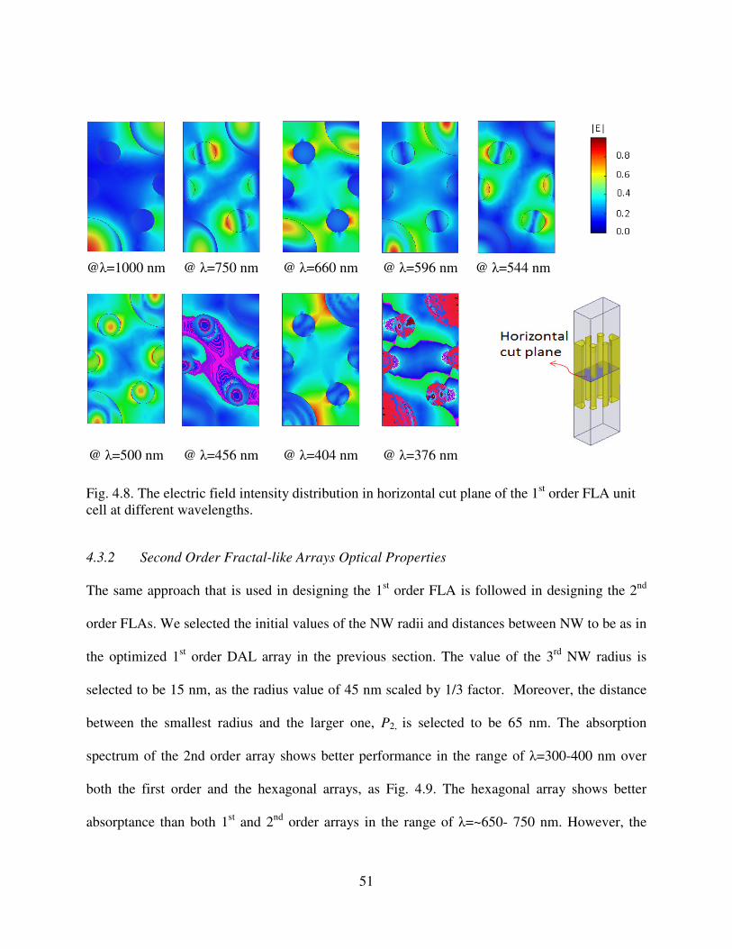
51
@λ=1000 nm @ λ=750 nm @ λ=660 nm @ λ=596 nm @ λ=544 nm
@ λ=500 nm @ λ=456 nm @ λ=404 nm @ λ=376 nm
Fig. 4.8. The electric field intensity distribution in horizontal cut plane of the 1st order FLA unit
cell at different wavelengths.
4.3.2 Second Order Fractal-like Arrays Optical Properties
The same approach that is used in designing the 1st order FLA is followed in designing the 2
nd
order FLAs. We selected the initial values of the NW radii and distances between NW to be as in
the optimized 1st order DAL array in the previous section. The value of the 3
rd NW radius is
selected to be 15 nm, as the radius value of 45 nm scaled by 1/3 factor. Moreover, the distance
between the smallest radius and the larger one, P2, is selected to be 65 nm. The absorption
spectrum of the 2nd order array shows better performance in the range of λ=300-400 nm over
both the first order and the hexagonal arrays, as Fig. 4.9. The hexagonal array shows better
absorptance than both 1st and 2
nd order arrays in the range of λ=~650- 750 nm. However, the

52
total efficiency of the 1st and 2
nd order arrays is still higher than that of the hexagonal array, as in
Fig. 4.11. This is because the amount of power in the visible band of the solar spectrum is higher
than that in the IR band. The enhancement in the visible band, even with minor percentage, is
preferable over the IR band.
Fig. 4.9. Absorption spectra for thin silicon film, simple hexagonal, and 1st and 2
nd order fractal-
like SiNW array structures, for the height of 1.15 µm.
The electric field intensity of the 2nd
order DLA unit cell is plotted in Fig. 4.10 for horizontal cut-
plane at the middle distance of the array height. By comparing the electric field intensity
distribution profiles of the 1st order and 2
nd order DLA, Fig. 4.8 and Fig. 4.10, we can see that the
electric field distribution patterns are affected by the presence of the small radius nanowires,
especially in the surrounding space of the NW. The effect of the smallest radius NW on the
electric field distribution and the coupling between the fields in the nanowires is noticeable
nearly in the entire spectrum. We can see that the presence of the smaller radius NW in the 2nd
order array leads to change the electric field distributions in the NW and the surrounding regions.
0
0.1
0.2
0.3
0.4
0.5
0.6
0.7
0.8
0.9
1
300 400 500 600 700 800 900 1000
Ab
sorp
tan
ce
Wavelength [nm]
second order fractal-like array
Si thin film

53
For example, at λ= 596 nm, we can see that the mode of propagation looks like the LP modes of
optical waveguide, as seen in Appendix (A). This can be attributed to the change in the
surrounding medium of the NW due to the presence of extra smaller NW, which can be thought
of as changing the effective refractive index of the surrounding medium of the wire.
λ=1000 nm λ=750 nm λ=660 nm λ=596 nm λ=544 nm
λ=500 nm λ=456 nm λ=404 nm λ=376 nm
Fig. 4.10. Normalized electric field intensity patterns in a horizontal cut view of the 2nd
order
FLA unit cell at different wavelengths.
The absorption spectra of silicon film, optimized hexagonal, 1st order, and 2
nd order fractal-like
SiNW arrays with 1.15 µm heights are shown in Fig. 4.11. The 1st order array shows enhanced
absorptance in the range of λ=300-~500 nm over the uniform hexagonal array. In this band of
wavelengths, the absorption level is almost greater than 0.85. In the range of λ=700 nm, the
absorptance of the 1st order array is enhanced significantly over that of the hexagonal array.

54
Fig. 4.11. Absorption spectra of thin film, simple hexagonal with R = 180 nm, 1st order with
1R =
135 nm and2R = 45 nm, and 2
nd order FLA arrays with
1R =125 nm, 2R =35 nm and
3R = 15 nm.
The array and thin film are of 1.15 µm heights.
Table 4.1 shows the efficiency and the filling ratio for thin film, hexagonal, 1st and 2
nd order
array structures calculated at two different heights, 1.15 and 2.3 µm. The effect of doubling the
height of the SiNW on the efficiency is more obvious for the 1st order array. The enhancement in
the efficiency and filling ratio of each structure relative to the equivalent thin film is shown.
Table 4.1- Filling ratio and efficiency of the simulated SiNW arrays
Thin film
Hexagonal array
1st order array
2nd
order array
Height
1.15µm
Efficiency ~10.0% ~17.5% ~18.9 % ~19.2%
Filling ratio 100% ~34.0% ~24.6% ~23.0%
Height
2.30µm
Efficiency ~14.0% ~21.8% ~26.1% ~22.4%
Filling ratio 100% ~34.0% ~24.6% ~23.0%
0
0.1
0.2
0.3
0.4
0.5
0.6
0.7
0.8
0.9
1
300 400 500 600 700 800 900 1000
Ab
sorp
tan
ce
Wavelength [nm]
Simple hexagonal array
first order fractal-like array
second order fractal-like array
Si thin film

55
4.3.3 Nanowire Height Effect
The effect of the height of the array is studied in this section for the 1st and 2
nd order FLA with
optimized dimensions as given in the previous sections. The height is increased in 250 nm
increment step, where the ultimate efficiency of each arrays is calculated. The effeceincies of the
arrays as function of their heights are shown in Fig. 4.12. The enhancement of the efficiency, as
a result of increasing the height of the arrays is clear for all arrays. The effeceincy of the 1st and
the 2nd
order arrays are close to that of the hexagoanl array at hieghts up to 1.8µm. In this case,
the advantage of the 1st and 2
nd order arrays over the simple hexagonal array is only the
reduction of the matrial amount, which is represented by filling ratio. Above 1.8 µm height, the
1st order array has higher effeciency than the other array structures. At 2.3 µm height, the
effeceincy of the 1st order array is ~26%, whereas it is ~22% for hexagonal array. This represents
~18% enhancemnt over the efficiency of the hexagoanl array. The 1st order array filling ratio is
reduced by ~25.5% of that of the hexagonal array. For the 2nd
order, the enhacemnt of the
effeciency over the hexagonal array is minor, but the reduction of the material amount is ~32%.
Fig. 4.12. The efficiency of cSi film, simple hexagonal, and 1st and 2
nd order fractal-like
structures against the array height [67].

56
4.4 Optimization of the Parameters of the Fractal-Like Array
Due to the multiple parameters in the FLA configuration, we adopted simple optimization
strategy to find optimal parameters in the sense of filling fraction and ultimate efficiency. In this
section we conduct optimization on the 1st order FLA using two approaches. The first is to study
the effect of NW positioning while keeping all other dimensions of the array, ( &W L ), constant.
The second is to scale the entire unit cell dimensions, including the NW, to find optimal cell size.
By this means, we optimize the array dimensions in limited number of possible parameter
combinations. The optimization of the array in more efficient ways that might result in better
performance parameters can be conducted using heuristic optimization techniques, which we will
consider for future study.
4.4.1 Nanowire Positions Optimization
As mentioned earlier in Section (4.3.1), optimization results of the 1st order array with respect to
the radii (1R and
2R ) is performed and resulted out the optimal radii dimensions. In the current
section, we conduct optimization by sweeping the three parameters, the NW radii 1R and
2R , and
the position of the smaller radius,1R as shown in Fig. 4.6, while the unit cell dimensions,
W and L , are kept constant. Figure 4.13 shows the ultimate efficiency in colored scale and with
numeric value inserted in the figure, calculated at different position distances between the
smaller radius and larger radius NWs, 1P . The sweeping of the parameters are conducted with 10
nm increment step for the radii values, and 20 nm for the position value1P .

57
Fig. 4.13. Optimization of the ultimate efficiency for the NW radius of the 1st order FLA with
1.15 µm height, performed at different positions: (a) 1P =200 nm, (b)
1P =220 nm, (c)1P =240 nm,
(d)1P =260 nm. The efficiency value is color and numerically inserted in the figure.
It is clear that changing the position affects the efficiency and plays a role in obtaining the
optimal position parameters for the efficiency. The conducted optimization shows that despite
the filling fraction of the array is kept constant, the efficiency changes as the position of smaller
radius NW changes within the unit cell. This tells that the filling fraction is not the only
parameter that controls the performance of the array, but also the geometrical parameters
including distance between NWs. This conclusion tells that SiNW arrays of a low filling fraction
can be produced with high efficiency if properly designed. This obtained results shows that the
optimal performance of array is obtained with distances and NW radius dimensions close the
fractal dimensions, where the fractal scaling factor is 1/3.

58
4.4.2 Unit Cell Size Optimization
Optimization of the unit cell size for ultimate efficiency is performed to explore the potentials of
the arrays in achieving more enhanced performance. The optimization is based on scaling the
size of the unit cell including the SiNW. By this manner, the filling fraction is kept constant, ~
24.6%, whereas the NW radii and the cell size are scaled with the same percentage. The
optimization is performed for FLA of height of 1.15 µm. By making comparison between the
ultimate efficiency of thin film and this optimized FLA, we can see that for thin film of 1.15 µm
thickness, the efficiency is ~ 10% , whereas for the scaled first order FLA with a height of 1.15
µm the efficiency can reach as high as ~22% , as Fig. 4.14. This means ~ 75% saving in the used
material and 110% enhancement over the ultimate efficiency of thin film.
Fig. 4.14. The ultimate efficiency vs. the unit cell size as scaled relative to initial unit cell size
&W L are 300 nm and 520 nm, respectively.
Summary
In this chapter, we present a new SiNW array configuration, inspired by fractal geometry.
Hexagonal fractal-like geometry has been adopted to design fractal-like SiNW arrays. The

59
fractal-like SiNW array configurations have been studied, and the effect of fractal-like lattice
configuration on enhancing the absorption spectrum of the array is tested. The efficiency of the
proposed fractal-like SiNW arrays achieve ~100% enhancement over that of the equivalent
thickness flat cSi film, and ~18% enhancement over an equivalent height regular uniform
hexagonal array. The proposed optimized structures achieved a filling ratio of ~25% which is
~33% less than the corresponding hexagonal array. The proposed fractal-like arrangement of
SiNW arrays yield broad absorption spectrum and enhanced efficiency while using less material.
The achieved efficiency compared with cSi flat film of equivalent thickness is significantly
enhances. Different parameters such as the SiNW heights, diameter, and relative positions, are
key elements to enhance the performance of the FLA arrays. Due to the multiple parameters
associated with fractal-like array geometries, heuristic optimization techniques would be more
efficient in studying, enhancing performance, and designing fractal-like arrays. Exploring the
potentials of the fractal –like configurations can be a topic for future stand-alone study.

60
CHAPTER 5
Diamond-Like SiNW Arrays
In the previous chapter, we introduced new SiNW fractal-like array (FLA) configurations that
show enhanced and broadened absorption spectrum. In the FLA, the arrangement and the values
of the NW radii are ruled by the fractal geometry. In this chapter, we introduce novel SiNW
array configuration inspired from the diamond lattice structure and employs radii diversity within
this lattice configuration. New strategy (rule) for arranging the diverse radius NW, in array unit
cell, are employed in this chapter that leads to enhanced performance in terms of efficiency and
the amount of used material. Optimization has been conducted to obtain optimal unit cell and
NW radii dimensions. Furthermore, the effect of angel of incidence and polarization are studied.
Finally the concept of the diamond-like array (DLA) is applied to silicon nano-cone (SiNC)
arrays.
5.1 Principles of Designing the DLA
The effects of radial diversity, lattice configuration, and the arrangemnt of SiNW on a
lattice configuration effects on the absoprtion spectrum of an array are studied Chapter 3. Since
there are unlimied number of permutations in which we can arrange NW with diversity in
difference lattice configurations, we consider a lattice that is inspired by diamond crystal lattice
structure. We employ the concept of radial diveristy by including the different radii NW in a
periodic unit cell that has a top view that looks like the 100 view of the diamnd lattice unit cell,
as Fig. 5.1 demonstrates. This is the reason why we coin the name of dimanod-like array (DLA)
to these array confugurations. In DLA configurations, thirteen NW can be arranged in a square
periodic cell. We follow a certain strategy in arranging diverse NW in the unit cell that leads to
optimal filling fraction and ultimate efficiency. This strategy is based on positioning the largest
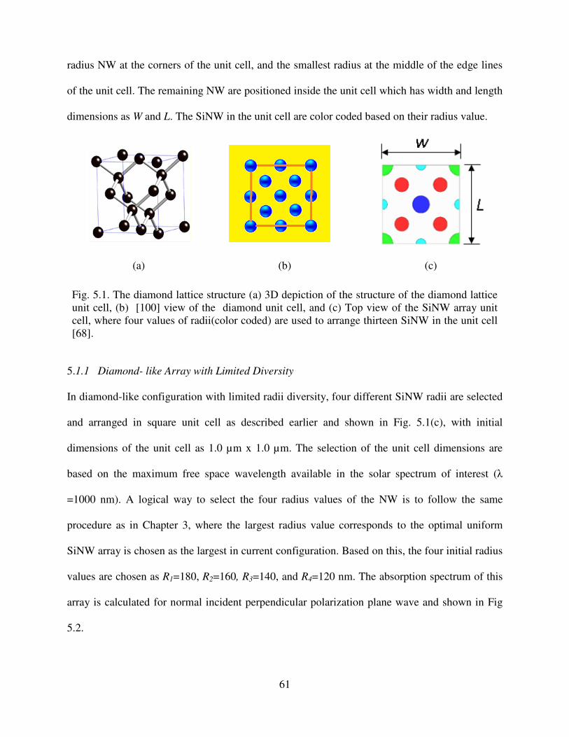
61
radius NW at the corners of the unit cell, and the smallest radius at the middle of the edge lines
of the unit cell. The remaining NW are positioned inside the unit cell which has width and length
dimensions as W and L. The SiNW in the unit cell are color coded based on their radius value.
(a) (b) (c)
Fig. 5.1. The diamond lattice structure (a) 3D depiction of the structure of the diamond lattice
unit cell, (b) [100] view of the diamond unit cell, and (c) Top view of the SiNW array unit
cell, where four values of radii(color coded) are used to arrange thirteen SiNW in the unit cell
[68].
5.1.1 Diamond- like Array with Limited Diversity
In diamond-like configuration with limited radii diversity, four different SiNW radii are selected
and arranged in square unit cell as described earlier and shown in Fig. 5.1(c), with initial
dimensions of the unit cell as 1.0 µm x 1.0 µm. The selection of the unit cell dimensions are
based on the maximum free space wavelength available in the solar spectrum of interest (λ
=1000 nm). A logical way to select the four radius values of the NW is to follow the same
procedure as in Chapter 3, where the largest radius value corresponds to the optimal uniform
SiNW array is chosen as the largest in current configuration. Based on this, the four initial radius
values are chosen as R1=180, R2=160, R3=140, and R4=120 nm. The absorption spectrum of this
array is calculated for normal incident perpendicular polarization plane wave and shown in Fig
5.2.

62
Fig. 5.2. Schematic of the diamond-like diverse radii SiNW array (a) 3D depiction of part of
the infinite array. (b) Top view of the array (c) Top view of the unit cell, four values of
radii(color coded) are used to arrange thirteen SiNW in the unit cell.
Figure 5.3 shows the absorption spectrum and the reflectance of this array. The calculated
ultimate efficiency of this array is ~ 33%, which is a large enhancement in the efficiency of ~
50%, over the uniform array. The absorption level is enhanced and broadened significantly in the
range of IR band. This shows the advantage of diversifying of NW radii coupled with proper
arrangement via DLA configuration. However, the absorptance level is below ~ 90% for nearly
the entire spectrum and the filling fraction is ~ 47%. The obtained result, shown in Fig. 5.3 tells
that high absorption level in the IR band is highly enhanced, whereas the visible spectrum shows
moderate enhancement. Since enhancing absorption level in the visible spectrum is more
important in the PV applications, we conduct parametric optimization of the NW radius values to
achieve better level of absorption in the visible band, reduce the filling fraction, and keep the
level of absorption in the IR band as high as possible. This led us to conduct optimization of the
array for ultimate efficiency and filling fraction using parametric analysis for the four values of
the NW radii. The optimization is performed by sweeping the values of the NW radius values
over certain ranges with 5 nm increment step.
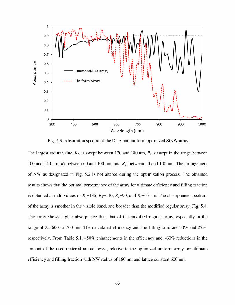
63
Fig. 5.3. Absorption spectra of the DLA and uniform optimized SiNW array.
The largest radius value, R1, is swept between 120 and 180 nm, R2 is swept in the range between
100 and 140 nm, R3 between 60 and 100 nm, and R4 between 50 and 100 nm. The arrangement
of NW as designated in Fig. 5.2 is not altered during the optimization process. The obtained
results shows that the optimal performance of the array for ultimate efficiency and filling fraction
is obtained at radii values of R1=135, R2=110, R3=90, and R4=65 nm. The absorptance spectrum
of the array is smother in the visible band, and broader than the modified regular array, Fig. 5.4.
The array shows higher absorptance than that of the modified regular array, especially in the
range of λ= 600 to 700 nm. The calculated efficiency and the filling ratio are 30% and 22%,
respectively. From Table 5.1, ~50% enhancements in the efficiency and ~60% reductions in the
amount of the used material are achieved, relative to the optimized uniform array for ultimate
efficiency and filling fraction with NW radius of 180 nm and lattice constant 600 nm.
0
0.1
0.2
0.3
0.4
0.5
0.6
0.7
0.8
0.9
1
300 400 500 600 700 800 900 1000
Ab
sorp
tan
ce
Wavelength (nm )
Series1
Series4
Diamond-like array
Uniform Array
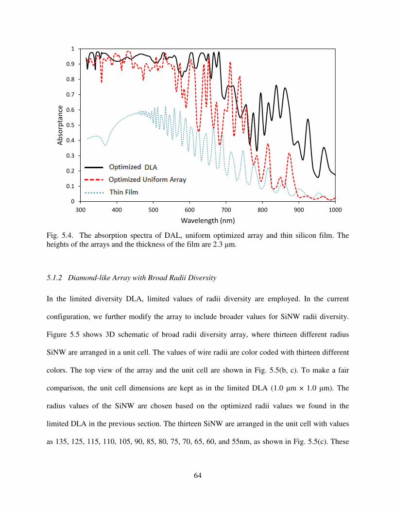
64
Fig. 5.4. The absorption spectra of DAL, uniform optimized array and thin silicon film. The
heights of the arrays and the thickness of the film are 2.3 µm.
5.1.2 Diamond-like Array with Broad Radii Diversity
In the limited diversity DLA, limited values of radii diversity are employed. In the current
configuration, we further modify the array to include broader values for SiNW radii diversity.
Figure 5.5 shows 3D schematic of broad radii diversity array, where thirteen different radius
SiNW are arranged in a unit cell. The values of wire radii are color coded with thirteen different
colors. The top view of the array and the unit cell are shown in Fig. 5.5(b, c). To make a fair
comparison, the unit cell dimensions are kept as in the limited DLA (1.0 µm × 1.0 µm). The
radius values of the SiNW are chosen based on the optimized radii values we found in the
limited DLA in the previous section. The thirteen SiNW are arranged in the unit cell with values
as 135, 125, 115, 110, 105, 90, 85, 80, 75, 70, 65, 60, and 55nm, as shown in Fig. 5.5(c). These
0
0.1
0.2
0.3
0.4
0.5
0.6
0.7
0.8
0.9
1
300 400 500 600 700 800 900 1000
Ab
sorp
tan
ce
Wavelength (nm)

65
values are selected to cover the same range of radius values of that of the limited diversity DLA,
in previous section, but with more diverse values.
Fig. 5.5. Schematic of the broad diversity SiNW array (a) 3D depiction of part of the infinite
array. (b) Top view of the array. (c) Top view of the unit cell, contains thirteen different radii
(color coded) [68].
The array has strong absorptance covering the visible and the near IR. The absorptance in the
visible band almost has the same trend as the limited DLA. In the near IR, significant
enhancement in the absorptance relative to all other arrays is clearly seen in Fig. 5.6. The filling
ratio for this structure is ~19%. That is, reduction in the amount of the material of ~66% relative
to the optimized uniform array for filling fraction and efficiency. This means that employing
broad diversity in SiNW not only enhances the absorptance, but also reduces the amount of the
used material. Both of the diamond-like array structures exhibit high absorptance in the visible
band. The broad diversity array shows significantly enhanced absorptance in the near IR. The
absorptance spectrum of the broad diversity array is near to the ideal unity absorptance spectrum.
The efficiencies and the filling fractions of the four array structures are shown in Table 5.1. A
trend in the efficiency enhancement is obvious as modifying uniform arrays from simple into
more diverse radius arrays.

66
Fig. 5.6. Absorptance spectra of the array structures: (black solid) diamond-like array with
broad diversity arrays, (red dashed) limited diversity diamond-like diverse, and (blue dashed)
thin silicon film. The heights of all arrays and the film are 2.3 µm.
Reduction in the amount of the material, as the array becomes more diverse, is another trend can
be noticed form Table 5.1. Enhancement in the efficiency and filling fraction are quite clear for
all the array configurations, relative to equivalent thickness crystalline silicon film. Ultimate
efficiency, as high as 35%, is achieved with a filling ratio of ~19% for the broad diversity array.
Reduction of ~81% in the amount of the used material, and enhancement on the efficiency of
150% are achieved relative to equivalent thickness silicon film.
Table-5.1. Ultimate efficiency and filling fraction of thin film and for SiNW arrays
Thin Film Optimized
uniform
array
Diamond-
like
With limited
diversity
array
Diamond-like
with broad
diversity
array
Ultimate Efficiency
~14.0%
~22.3%
~30%
~35%
Filling fraction 100% ~28.9% ~21% ~19%
0
0.1
0.2
0.3
0.4
0.5
0.6
0.7
0.8
0.9
1
300 400 500 600 700 800 900 1000
Abso
rpta
nce
Wavelength (nm)

67
5.2 Optimization of the Unit Cell Dimensions
In the DLA, diversity and distribution of the NW are deployed to produce an enhanced
absorption spectrum. The radius values are selected in a manner to produce an absorption
spectrum that has multiple peaks. The initial unit cell dimensions and radius values lead to an
enhanced and broadened absorption spectrum over uniform periodic arrays [69]. Further
optimization is conducted for the ultimate efficiency of the limited diversity array. Since the
array includes large number of parameters, the optimization is performed in two ways. In the
first, NW radii are scaled while fixing the cell size; in the second, both the cell size and the NW
radii are scaled. In the first case, the ultimate efficiency vs the filing fraction is shown in Fig.
5.7(a). In the second case, the filling fraction is kept constant as the initial value of 24%, and
ultimate efficiency vs scaling factor is shown in Fig. 5.7(b). Ultimate efficiency as high ~34%
can be achieved with ~50% filling fractions. The optimal performance of the array, in the sense
of filling fraction and ultimate efficiency, is achieved at scaling factor of 1.3 of the initial cell
structure, as shown in Fig. 5.7(b). An interesting result out of the optimization of DLA is that
the ultimate efficiency can exceed 20% with a filling fraction as low as ~11%, as Fig. 5.7(a)
shows. The absorption spectrum of the optimized array is shown in Fig. 5.8.
Fig. 5.7. (a) Fixed lattice constant, variable radii value using 10% scaling increments, (b) Fixed
filling fraction (24%) with scaling of the unit cell and the radii values in 10% increments[68].

68
Broad diversity is shown to enhance the performance of the uniform periodic arrays, in the sense
of the ultimate efficiency and the amount of material, as demonstrated in Section (3.2). Broad
diversity is applied to the DLA, which leads to enhance the absorption over the entire solar
spectrum as shown in Fig. 5.8. The absorption level of the diverse DLA outperforms all of that of
other arrays over the entire spectrum. The enhancement of absorption over uniform periodic
arrays is significant especially in the IR band in the diverse arrays. For the broad diversity SiNW
arrays, the enhancement is quite remarkable. Optimization is conducted to the initial broad
diverse DLA structure in a similar manner to the limited diversity arrays. The initial filling
fraction (~19%) is kept constant, and the optimal scaling factor is found to be ~1.3, similar to
that of the limited diversity DLA.
Fig. 5.8. Absorption spectra of thin film, limited diversity DLA, and broad diversity DLA. The
height (h) of the film and the arrays is 2.3 µm.
The role of diversity in broadening and enhancing the absorption spectrum can be seen in Fig.
5.8. Both DLAs show almost the same absorption trend in the band of (λ=315-500 nm), which
means that the optical effects and absorption mechanisms are not affected by the diversity in this
0
0.1
0.2
0.3
0.4
0.5
0.6
0.7
0.8
0.9
1
300 400 500 600 700 800 900 1000
Ab
sorp
tan
ce
Wavelength (nm)

69
band. On the other hand, the absorption of the DLAs is significantly enhanced in the band of
greater than λ=~500nm over the uniform and modified periodic array. This indicates that other
optical effects arise as a result of the diversity which enhances absorption. Table 5.2 shows the
filling fraction for thin film, optimized uniform periodic array, modified periodic array, DLA
with limited diversity, and DLA with broad diversity. The role of employing diversity and the
DLA structure in enhancing the efficiency and filling fraction is clear in Table 5.2.
Table 5.2-. Ultimate efficiency and filling fraction for different optimized SiNW arrays
Thin Film Optimized
Uniform Periodic
array
DLA with limited
diversity
DLA with broad
diversity
Ultimate Efficiency ~13.8% ~22.3% ~32.6% ~39.5%
Filling fraction 100% ~28.9% ~22.6% ~19.1%
The achieved ultimate efficiency and filling fraction in the broad diversity DLA are superior to
all other types of SiNW arrays. The ultimate efficiency and the filling ratio are of the range of
~40% and ~19%, respectively. This means that ~77% enhancements in the efficiency and ~34%
reductions in the amount of the material are achieved, relative to the optimized uniform periodic
array. This confirms the role of diversity combined with the proper distribution in enhancing the
efficiency and reducing the material over the uniform periodic arrays.
5.3 Angular Response
In addition to many interesting features of the NW array, the wide angle response is another
important feature that distinguishes NW arrays. The response of the SiNW–DLA to the off
normal angle of incidence is tested for limited diversity DLA. The normal angle of incidence is
considered as 0°. Angle of incidence is incremented in 5° steps, where the reflectance,
transmittance and absorptance of the array are calculated. Figure 5.9 shows a 3D depiction of
the planes of incidence at different orientations with respect to the lattice configuration.

70
Fig. 5.9. 3D depiction of two planes of incidence for normal plane wave representing two
cases of parallel polarization with two orientation angles with respect t to the unit cell
orientation: (φ=0 ͦand φ=45). Parallel to, and at 45 to the lattice vector, labeled (10) and (11)
respectively.
To test performance of the DLA arrays under different angles of incidence, the angular response
is studied. In addition to perpendicular (s) and parallel (p) polarizations, the effect of the
orientation of the lattice to these polarizations is investigated. The two different orientations of
the plane of incidence relative to the lattice cell are labeled as 10 and 11, respectively, are shown
in the insets of Fig. 5.10. To quantify the angular response, the ultimate efficiency is calculated
at different off normal angles (θ). In Fig. 10(a, b) we show the ultimate efficiency as a function
of incidence angle. For comparison, we plot the angular response of optimized uniform SiNW
array (a= 600nm, a= 182nm). We can see that the DLA angular response has the same trend as
the uniform array. The response of the arrays is independent of the angle of incidence up to 70
degree and 60 degrees for in the p-polarization and s-polarization, respectively. The obtained
trend of the angular response is consistent with previous studies [19]. This increase of the
efficiency above that of the normal incidence can be attributed to the variant of resonances
modes that occur as a result of different angles of incidence [15].

71
(a) (b)
Fig. 5.10. The angular response of the limited diversity SiNW DLA at: (a) parallel, (b)
perpendicular polarizations at different orientations of the plane of incidence with respect to
the lattice structure expressed by 11 and 10 vectors[68]
For the off normal angel of incident (θ), the transverse wave vectors inside and outside the NW
can be expressed by2 2
sin ( )ok n= −κ θ , sin( )o
k=γ θ , and cos( )o
k=β θ , as shown in Fig. 5.11.
One can see that the wave vectors are functions of the angle of incidence. Referring back to the
transcendental equations, Appendix (A), we can see that the arguments of the Bessel functions
for normal incidence are Rκ and Rγ , where R is the NW radius. For the off normal incidence,
these arguments become as 2 2
sin ( )oR k R n= −κ θ and cos( )o
R Rk=γ θ [32, 35, 38]. The wave
vector dependence on the angle of incidence suggests that the excited leaky modes to be different
with angle of incidence. However, because the silicon refractive index is in the range of ~3.5 -
~8, the κ value is barely affected by most of the angles of incidence and renders as o
k n≅κ
[35]. The array has different angular response to the different polarizations of the incident wave,
as inferred from Fig. 5.11. In the case of the perpendicular polarization, in addition to the wave
vector factor, the cosine rule can be seen to take effect, where the wave can be analyzed into two
components, vertical and horizontal.

72
(a)
(b)
Fig. 5.11. Demonstration the off normal angle of incidence and the wave vector for: (a)
parallel polarization, and (b) perpendicular polarization.
The vertical component does not play a role in exciting propagating modes in the infinite NW
array, whereas the horizontal component is the effective in exciting the resonance modes.
5.4 Nanowires Height Effect on the Absorption Spectrum
In Chapter 3 we studied the effect of height of nanowire on the ultimate efficiency of SiNW
arrays. In the current section, the performance of the SiNW arrays as a function of the nanowires
height is studied for the limited diversity of DLA array. Simply, the limited diversity DLA
nanowire heights are increased from 500 nm up to 4000 nm in 500 nm increment step. The
absorption spectrum is calculated at each height and the absorption spectra are shown in Fig.
5.12. The height of the nanowires has different influence at different wavelength range of the
entire solar band of interest. We can see that as the height is increased the absorption level
increased up to 2500 nm. In the range of λ=300-~600 nm, increasing the height is not enhancing
the absorption significantly and the absorption spectrum is following the same trend. In other

73
words, the absorption spectrum starts to saturate at NW height of 2500 nm. Whereas in the range
of λ=~600-1000 nm, increasing the NW height has significant effect on the absorption spectrum.
We can see that as the height is increased the spectrum broadens and is enhanced. The relation
between the height and the absorption spectrum can be attributed to the silicon material
dispersive nature. On the one hand, absorption coefficient in the visible band is high and the
silicon is strong light absorber in the range of λ=300 -~450 nm. Therefore, the light is absorbed
in the top part of the NW and any further increase in the height (or bulk thickness in general)
would not enhance absorption level. On the other hand, silicon absorption in the IR band is
weak, therefore IR wavelengths needs longer propagation path to be absorbed efficiently.
Fig. 5.12. Absorption spectra of the silicon DLA at different heights.
We can see that the efficiency increases monotonically in the range of h=1000-3000 nm. In this
range, the absorption in the visible spectrum (λ=300–600 nm) is enhanced as the height increases
and saturates for the heights larger than ~ 3000 nm. The same applies in the IR band (λ> ~600
0
0.1
0.2
0.3
0.4
0.5
0.6
0.7
0.8
0.9
1
300 400 500 600 700 800 900 1000
Ab
sorp
tan
ce
Wavelength ( nm)
h=500nm
h=1000nm
h=1500nm
h=2500nm
h=3000nm
h=3500nm
h=4000nm

74
nm) except that one need to increase the height larger than 3000 nm to enhance the absorption
level. This can be attribute to the Fabry-Perot resonances that results in a longer effective path
which leads to more absorption. This is not the case in the visible, because the light is absorbed in
a few micrometers and Fabry-Perot effect is not dominant. The ultimate efficiency of the array is
calculated at different height of the array. Figure 5.13 show the ultimate efficiency as function of
the height. We can see that the efficiency increase rapidly as the height increases up 1000 nm,
then the slope decreases up to 3000 nm, where the efficiency starts to saturate. This trend is
attributed to the level of absorption in the visible light and the IR. The visible light absorption
level saturate at the height of ~ 2500 nm, whereas the IR absorption keeps increasing as the height
increases and considered responsible for the enhancement for heights larger than 3000 nm. But
since the photo density in the IR is relatively less, the increase is rather small.
Fig. 5.13. Ultimate efficiency against the height of the SiNW array calculated at 500
nm increment step.
5.5 Qualitative Analysis
Light interaction with SiNW arrays encompasses different optical effects. For weak absorbing
materials, as silicon in the IR band, these optical effects play a key role in determining NW
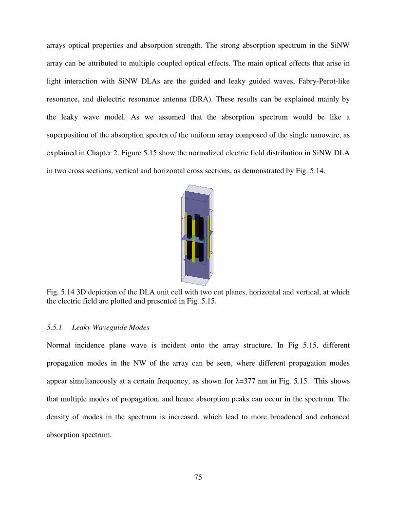
75
arrays optical properties and absorption strength. The strong absorption spectrum in the SiNW
array can be attributed to multiple coupled optical effects. The main optical effects that arise in
light interaction with SiNW DLAs are the guided and leaky guided waves, Fabry-Perot-like
resonance, and dielectric resonance antenna (DRA). These results can be explained mainly by
the leaky wave model. As we assumed that the absorption spectrum would be like a
superposition of the absorption spectra of the uniform array composed of the single nanowire, as
explained in Chapter 2. Figure 5.15 show the normalized electric field distribution in SiNW DLA
in two cross sections, vertical and horizontal cross sections, as demonstrated by Fig. 5.14.
Fig. 5.14 3D depiction of the DLA unit cell with two cut planes, horizontal and vertical, at which
the electric field are plotted and presented in Fig. 5.15.
5.5.1 Leaky Waveguide Modes
Normal incidence plane wave is incident onto the array structure. In Fig 5.15, different
propagation modes in the NW of the array can be seen, where different propagation modes
appear simultaneously at a certain frequency, as shown for λ=377 nm in Fig. 5.15. This shows
that multiple modes of propagation, and hence absorption peaks can occur in the spectrum. The
density of modes in the spectrum is increased, which lead to more broadened and enhanced
absorption spectrum.

76
@ λ = 1000 nm @ λ = 748 nm @ λ = 600 nm @ λ = 500 nm @ λ = 460 nm @ λ = 428 nm
@ λ = 400 nm @ λ = 377 nm @ λ = 352 nm @ λ = 333 nm @ λ = 315 nm
Fig. 5.15. Electric field distribution, naormalized, plotted at differnrt wavelengths in vertiacl and
hriantal cut planes, horizental and vertical of the DLA unit cell.
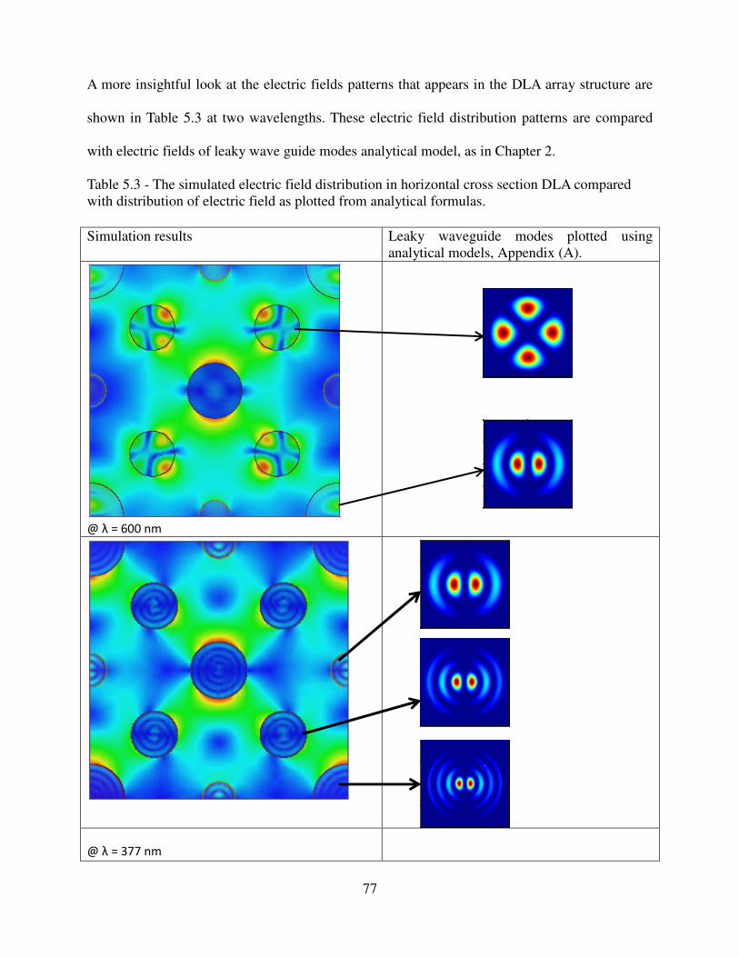
77
A more insightful look at the electric fields patterns that appears in the DLA array structure are
shown in Table 5.3 at two wavelengths. These electric field distribution patterns are compared
with electric fields of leaky wave guide modes analytical model, as in Chapter 2.
Table 5.3 - The simulated electric field distribution in horizontal cross section DLA compared
with distribution of electric field as plotted from analytical formulas.
Simulation results Leaky waveguide modes plotted using
analytical models, Appendix (A).
@ λ = 600 nm
@ λ = 377 nm
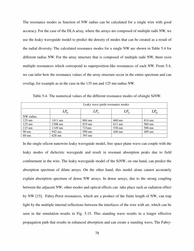
78
The resonance modes as function of NW radius can be calculated for a single wire with good
accuracy. For the case of the DLA array, where the arrays are composed of multiple radii NW, we
use the leaky waveguide model to predict the density of modes that can be created as a result of
the radial diversity. The calculated resonance modes for a single NW are shown in Table 5.4 for
different radius NW. For the array structure that is composed of multiple radii NW, there exist
multiple resonances which correspond to superposition-like resonances of each NW. From 5.4,
we can infer how the resonance values of the array structure occur in the entire spectrum and can
overlap, for example as in the case in the 135 nm and 125 nm radius NW.
Table 5.4- The numerical values of the different resonance modes of ofsingle SiNW.
Leaky wave guide resonance modes
01LP 11LP 21LP 02LP
NW radius
135 nm 1411 nm 884 nm 660 nm 614 nm
125 nm 1308 nm 819 nm 611 nm 569 nm
115 nm 1149 nm 721nm 538 nm 500 nm
90 nm 942 nm 590 nm 440 nm 409 nm
60 nm 628 nm 393 nm
In the single silicon nanowire leaky waveguide model, free space plane wave can couple with the
leaky modes of dielectric waveguide and result in resonant absorption peaks due to field
confinement in the wire. The leaky waveguide model of the SiNW, on one hand, can predict the
absorption spectrum of dilute arrays. On the other hand, this model alone cannot accurately
explain absorption spectrum of dense NW arrays. In dense arrays, due to the strong coupling
between the adjacent NW, other modes and optical effects can take place such as radiation effect
by NW [15]. Fabry-Perot resonances, which are a product of the finite length of NW, can trap
light by the multiple internal reflections between the interfaces of the wire with air, which can be
seen in the simulation results in Fig. 5.15. This standing wave results in a longer effective
propagation path that results in enhanced absorption and can create a standing wave. The Fabry-

79
Perot-like resonances are dominant in the IR band, which explains the strong absorption level of
IR despite silicon is weak absorptance in this band. The weakly guided modes and (Fabry-Perot)-
like resonances are the two main optical effects that are responsible for the peaks in SiNW arrays
absorption spectra. In a dielectric wave guide, under specific conditions, leaky guided waves can
radiate in radial directions making the dielectric circular cylinder acting like optical antenna [55].
Reference [55] contains detailed analysis about the conditions under which a dielectric
waveguides behaves as radiating optical antenna. This effect in SiNW arrays helps in deflecting
the normal incident light into lateral propagation. This can be seen as creating an infinite path
length for light propagation. The radiated light from the NW is either absorbed or scattered in a
Mie-like scattering by the neighboring NW. Radii diversity results in an increase of the density
of the modes in an array, which increases the probability that NW act as an optical antenna at
different modes. These intuitive analyses can explain the significant enhancement of absorption
in SiNW DLA, especially in IR band. The broadening and enhancement of the absorption
spectrum in SiNW DLA can be attributed to the above mentioned optical effects. We emphasize
that at specific regions in solar spectrum there are particular dominant optical effects [68].
5.5.2 Lateral Propagation of Light
The lateral power flow in the array structure is tested at different wavelengths. To calculate the
lateral power flow, Poynting vector is integrated over a vertical surface imposed to the structure
as shown in inset in Fig.5.16. The net normal power flow through this surface is calculated as:
( ).S
W Re P n ds= ∫�
�
(5.1)
where P�
is the Poynting vector, S is the surface, and n�
is the normal of this surface. Figure 5.16
shows the total normal power flow though a circular cylinder wall (surface) calculated at

80
different wavelengths of the spectrum. By this configuration of integration surface, we calculate
only the normal component of Poynting vector. It is obvious that in the IR wavelengths range
that there is a significant lateral power flow. We can see that the broad diversity array exhibits
more lateral power propagation than that of the limited diversity array, especially in the λ= ~550-
1000 nm, which explains the superiority of the absorption. This tells that the structure in this
manner support the diverting of the normally incident light into laterally propagating light,
especially in the IR band. This results in infinite length effective propagation path and explains
the high absorption level in the IR band.
Fig. 5.16. Normalized net power flow in the latteral direction to the normal incident light on
the DLA. Th inset shows the cylindrical surface planne on which Poynting vector is integrated
In addition to the these different effects we can see that localized field resonances can appear in
the array structure, as the electric field intensity distribution pattern suggest, Fig 5.15. These
0
0.02
0.04
0.06
0.08
0.1
0.12
0.14
0.16
0.18
0.2
300 400 500 600 700 800 900 1000
No
rma
lize
d P
ow
er
Wavelength ( nm)
Limited Diversity DLA
Broad Diversity DLA

81
localized fields have a role in light trapping in the array structure and hence the optical properties
of the array.
5.6 Silicon Nano Cones
It has been proven that radial diversity significantly enhances the absorption spectrum for SiNW
array. The diversity coupled with proper arrangement in the DLAs shows near-unity ideal
absorption spectrum. A logical way to implement radial diversity is via cone morphology. We
can think about nano-cone as a NW which is composed of multiple of NW of continuum
diversity of radii values. In fact, NC arrays have been reported to enhance the absorption
spectrum in GaAs NC [71], which is a direct band gap material with high absorption coefficient.
One way to explain the superiority of the NC arrays is that they have gradual change of the
effective refractive index, which makes the incident wave impedance easily coupled with the
array structure.
5.6.1 Uniform SiNC Array
The SiNC arrays have remarkable optical properties and the potentials for enhancing the
electrical properties of a PVSC device. Parametric analysis has been done to find the optimal
parameters of SiNC. The analysis is based on sweeping three parameters of the array: the lattice
constant, the top and bottom radius of the SiNC, Fig. 5.17. The lattice constant parameter, a,
range is set between 300-800 nm , the top radius range, Rt, is set between 30- 100 nm , and the
range of the bottom radius, and Rb, is set from 120 nm to 250 nm. The ultimate efficiencies of
these SiNC arrays at different parameter permutations are calculated. The height of the NC is set
to 2.3 µm for all the simulation runs. At each lattice constant value, parametric sweeping is
performed for the top and bottom radii of the NC. The efficiency of the array is calculated at
each lattice constant, and at the different values of the Rb and Rt.

82
(a) (b) (c) (d)
Fig. 5.17. (a) 3D depiction of a uniform periodic SiNC array, and top view of the unit cell
used in simulation domain. a represents the lattice constant.
Then, the maximum achieved efficiency at each lattice constant value with the permutations of Rt
and Rb is calculated, with 10 nm increment steps of the radii and 20 nm for the lattice constant.
This optimal lattice constant which is a=540, and the Rt and Rb as 220 and 70 nm respectively.
Figure 5.18 shows the absorption spectrum of the optimized SiNC array.
Fig. 5.18. The absorption spectrum of SiNC array suspended in air, the height is 2.3 µm, the
lattice constant, a, is 540 nm with top and bottom radii as 70 and 220 nm successively.
0
0.1
0.2
0.3
0.4
0.5
0.6
0.7
0.8
0.9
1
300 400 500 600 700 800 900 1000
Ab
sorp
tan
ce
Wavelength ( nm )
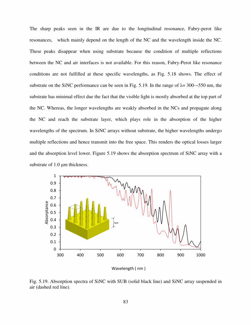
83
The sharp peaks seen in the IR are due to the longitudinal resonance, Fabry-perot like
resonances, which mainly depend on the length of the NC and the wavelength inside the NC.
These peaks disappear when using substrate because the condition of multiple reflections
between the NC and air interfaces is not available. For this reason, Fabry-Perot like resonance
conditions are not fulfilled at these specific wavelengths, as Fig. 5.18 shows. The effect of
substrate on the SiNC performance can be seen in Fig. 5.19. In the range of λ= 300-~550 nm, the
substrate has minimal effect due the fact that the visible light is mostly absorbed at the top part of
the NC. Whereas, the longer wavelengths are weakly absorbed in the NCs and propagate along
the NC and reach the substrate layer, which plays role in the absorption of the higher
wavelengths of the spectrum. In SiNC arrays without substrate, the higher wavelengths undergo
multiple reflections and hence transmit into the free space. This renders the optical losses larger
and the absorption level lower. Figure 5.19 shows the absorption spectrum of SiNC array with a
substrate of 1.0 µm thickness.
Fig. 5.19. Absorption spectra of SiNC with SUB (solid black line) and SiNC array suspended in
air (dashed red line).
0
0.1
0.2
0.3
0.4
0.5
0.6
0.7
0.8
0.9
1
300 400 500 600 700 800 900 1000
Ab
sorp
tan
ce
Wavelength ( nm )

84
5.6.2 DLA Silicon Nano Cone Arrays
The concept of the DLA is applied to the SiNC arrays, where different bottom radii NCs are
arranged in a diamond like configuration. We follow the same strategy used in the SiNW DLA in
arranging the diverse radii NW, where in that strategy the larger bottom radius NW are
positioned in the corners of the unit cell and the smallest radius in the center of the edges of the
unit cell. Figure 5.20 shows the unit cell and the NC, color coded based on the bottom radius
value, where four different values of the bottom radius are selected based on the optimal values
obtained for regular SiNC. The large Rb value is 130 nm and the other values are selected by
decrementing value of 20 nm. In all NCs, the top radius value is kept fixed at 40 nm.
Fig. 5.20. 3D depiction of a SiNC array in diamond-like array configuration and the unit cell
top view where W and L are 800 nm.
Figure 5.21 below shows the absorptance spectrum of the SiNC DLAs at different scaling values
of the unit cell. The same unit cell scaling optimization approach that is followed in SiNW-DLAs
in the previous section is followed here. The unit cell (simulation domain) size is scaled by factor
in the range of 0.9 to 1.3. The absorption spectra at different scales are plotted in Fig. 5.21,
where it is obvious that at the scaling factor of 1.3 of initial unit cell, the highest efficiency is
achieved. The dimensions of the unit cell in this case are ~1000 1000× nm. One can see that
for the range of λ=300-~550nm, the absorptance in the different scaling factor cases is almost

85
similar. Whereas in the range of λ> ~500nm the scaling of the size of the unit cell highly affect
the absorption spectrum behavior. This the same notice we found as in the DLA of SiNW.
(a) (b)
(c) (d)
Fig. 5.21. The absorption spectra of the SiNC-DLA at different scales of the unit cell dimensions
that are multiplied by a scaling factor between 0.9 to 1.3, where the initial unit cell dimensions
are 800 by 800 nm as in Fig. 5.20.
Figure 5.21 shows the absorption spectrum of the DL-SiNC array at different scales of the unit
cell size. We can observe that the absorption spectrum in the band of λ=300-600 nm. This means
that the optical effects are not highly affected in this range by scaling the unit cell. Whereas, one
can see that as the scaling factor increases, the absorption spectrum is broadened and enhanced in
0
0.2
0.4
0.6
0.8
1
300 400 500 600 700 800 900 1000
Ab
sorp
tan
ce
Wavelength (nm)
Scaling factor = 0.9 , η= 25.9%
Scaling factor = 1.0, η= 28.9%
0
0.2
0.4
0.6
0.8
1
300 400 500 600 700 800 900 1000
Ab
sop
rta
nce
Wavelength (nm)
Scaling factor = 1.0, η= 28.9%
Scaling factor = 1.1, η= 31.1%
0
0.2
0.4
0.6
0.8
1
300 400 500 600 700 800 900 1000
Ab
sop
rta
nce
Wavelength (nm)
Scaling factor = 1.1, η= 31.1%
Scaling factor = 1.2.,η= 31.7%
0
0.2
0.4
0.6
0.8
1
300 400 500 600 700 800 900 1000
Ab
sorp
tan
ce
Wavelength (nm)
Scaling factor = 1.2.,η= 31.7%
Scaling factor = 1.3, η= 32.9%

86
the range of λ=600-1000 nm. By increasing the scale factor the size of the unit cell and the radii
of the NC are increased simultaneously. In Fig. 5.21(e), one can see that the absorption in the IR
band is significantly enhanced, if compared with absorption spectrum in Fig. 5.21(a). The
absorption spectra of the scaled SiNC array are plotted and compared for the successive scaling
factors. We noticed that as the scale factor increases the absorption peaks red-shifts as can be
seen in Fig. 5.21(a-d). In addition to the red-shift, the peaks have stronger absorption level. The
scaling factor of the unit cell has optimal value in a similar manner to DLA SiNW array as Fig.
5.7. The observed phenomenon is that the absorption peaks position and their level are related to
the radii value of the NC and the lattice constant. As example, Fig. 5.2(d) shows that by scaling
up the cell size from 1.2 to 1.3, the absorption peaks at λ=730 nm , in 1.2 scaling, red-shifts to
λ=756 nm and become stronger. This red-shift is observable almost in all the IR spectrum and
can be attributes to the change in the radii value and lattice constant of the array. The optimal
scaling factor is found to be 1.3 for the current SiNC array, which means that there are optimal
values of the NC radii and lattice constant of the array at which the light is highly confined and
absorbed in the array structure. One can see that scaling up the unit cell enhances and broadens
the absorption of light in SiNC array. This enhancement of the absorption in the IR band
minimally compromises the absorptance in the visible band. Qualitatively, the enhancement of
the absorption in the IR is related to the distances in between the NC, which in the order of the
free space half wave length for the case of 1.3 scaling factor.
Diamond-like SiNC array with substrate show remarkable enhancement over the SiNC array
without substrate. Figure 5.22 show the absorption spectrum of the array where ultimate
efficiency as high as ~39% is achieved in this configuration

87
Fig. 5.22. Absorption spectrum of Diamond-Like SiNC array over silicon substrate. The heights
of the NCs are 2.3 µm.
Summary
In this chapter we introduced new SiNW array configurations that are inspired by the diamond
crystal lattice structure. Radial diversity of NW and proper arrangement are incorporated in the
design of these arrays. Two types of arrays are studied, with limited and broad radial diversity.
Optimization using parametric analysis is performed on the arrays for the ultimate efficiency and
filling fraction. The effect of the NW height on the array performance is studied. Moreover, the
angular response of the arrays is studied at different polarizations. As logical implementation of
radial diversity, SiNC are introduced, and the concept of DLA is applied to the SiNC in the form
of diamond-like SiNC arrays. The SiNW DLAs show significant enhancement in the ultimate
efficiency as high ~186% over equivalent thickness thin film, and material reduction in the order
of ~81%. By employing broad diversity of NW radii in DLA, broadband near-unity absorption
spectrum is achieved. The obtained results indicate that SiNW DLA with broad diversity of radii
has superior performance over other SiNW arrays configurations. The enhanced absorption of
the arrays persists for wide off normal incidence angel at different polarizations..
0
0.2
0.4
0.6
0.8
1
300 400 500 600 700 800 900 1000
Ab
sorp
tan
ce
Wavelength ( nm )

88
CHAPTER 6
Silicon Nanowire-Based Solar Cells
In the last three chapters, we have focused on studying optical properties of SiNW arrays. We
have shown that SiNW and SiNC arrays can achieve strong light trapping and absorption, that
make them very promising for fabricating high efficiency thin film PVSC devices. The next
logical step to follow would be to utilize such SiNW and SiNC arrays to fabricate high efficiency
thin film PVSC device. Unfortunately, the efficiency of PVCS device depends on many factors,
such as carrier’s recombination losses, collection efficiency, and ohmic losses. Therefore, this
chapter is set to investigate the performance of PVSC based on SiNW by using numerical
modeling. In fact, numerous analytical and numerical models of the radial junction PVSC have
been introduced in the literature, that offer valuable analytical models about the NW PVSC [71]–
[76]. In these models, to simplify the analyses, different assumptions are invoked such as
assuming a single NW PVSC with infinite length. In order to have physically realistic
estimations from an analytical model, different coupled physical mechanisms need to be
considered, which renders such analytical model quite complicated to solve. Moreover, for many
geometrical configurations, the analytical solution is not obtainable. For these reason, global
numerical modeling simulation that takes all of these coupled physical mechanisms in
consideration is adopted in this work by using SILVACO software packages. First, we introduce
analytical model for PN radial junction PVSC, and compare it with numerical simulation. Then,
optical properties of PiN junction PVSC, based on SiNW array, are introduced. Later, due to
limitation of software, PiN PVSC that is based on single SiNW is investigated. Finally, the effect
of NW geometry on PVSC electrical properties is tested.
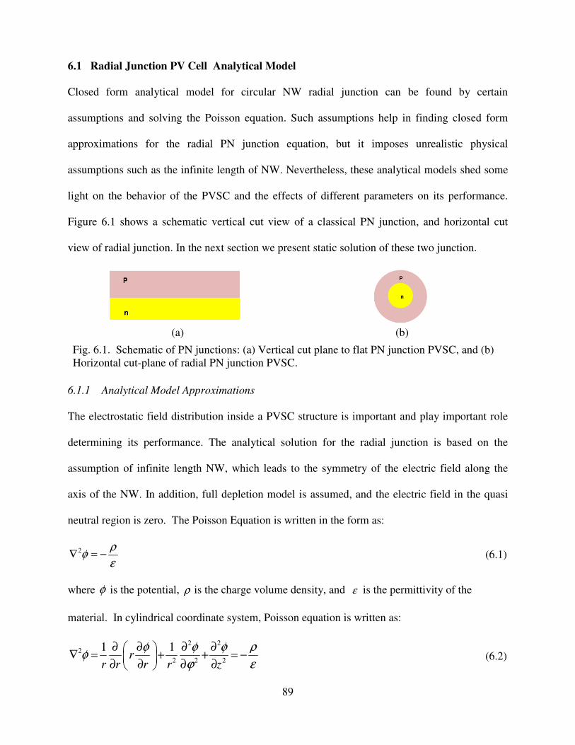
89
6.1 Radial Junction PV Cell Analytical Model
Closed form analytical model for circular NW radial junction can be found by certain
assumptions and solving the Poisson equation. Such assumptions help in finding closed form
approximations for the radial PN junction equation, but it imposes unrealistic physical
assumptions such as the infinite length of NW. Nevertheless, these analytical models shed some
light on the behavior of the PVSC and the effects of different parameters on its performance.
Figure 6.1 shows a schematic vertical cut view of a classical PN junction, and horizontal cut
view of radial junction. In the next section we present static solution of these two junction.
(a) (b)
Fig. 6.1. Schematic of PN junctions: (a) Vertical cut plane to flat PN junction PVSC, and (b)
Horizontal cut-plane of radial PN junction PVSC.
6.1.1 Analytical Model Approximations
The electrostatic field distribution inside a PVSC structure is important and play important role
determining its performance. The analytical solution for the radial junction is based on the
assumption of infinite length NW, which leads to the symmetry of the electric field along the
axis of the NW. In addition, full depletion model is assumed, and the electric field in the quasi
neutral region is zero. The Poisson Equation is written in the form as:
2 ρφ
ε∇ = − (6.1)
where φ is the potential, ρ is the charge volume density, and ε is the permittivity of the
material. In cylindrical coordinate system, Poisson equation is written as:
2 22
2 2 2
1 1r
r r r r z
φ φ φ ρφ
ϕ ε
∂ ∂ ∂ ∂ ∇ = + + = −
∂ ∂ ∂ ∂ (6.2)

90
By assuming circular symmetry along the cylinder axis, Poisson’s equation reduces into ordinary
differential equation of r as:
2
2
( ) 1 ( ) ( ) ( )d r d r dE r E r
dr r dr dr r
φ φ ρ
ε+ = − − = − (6.3)
where φ is the potential energy difference between intrinsic level and Fermi level which is set to
zero. The solution of this differential equation is as:
2( ) ln( )4
r r A r B= − + +ρ
φε
(6.4)
where A and B are constants. This leads to the electric field formulation as:
( )2
AE r r
r
ρ
ε= − (6.5)
Equation (6.5) shows the electric field distribution as a function of the radial distance. In order to
find the constants in this equation, the charge density and the boundary conditions need to be
specified. Detailed analyses of the NW have been reported in literature for different cases that
can occur in such radial junctions [74]. The following table shows the main governing equations
of PVSC operation for two configurations, flat junction and radial junction.
Table 6.1-The governing equation of planar and radial junction PVSC [74], [59].
Set of equations governing planar solar cell Summary of the governing equations in an
ideal radial junction solar cell
( )( ( ) ( ) )
a d
dE x qp x n x N N
dx
− += = − − +ρ
ε ε
( ) ( )( ( ) ( ) )
a d
dE r E r qp r n r N N
dr r
− ++ = = − − +ρ
ε ε
( )p p p
dpJ q p E x qD
dx= µ + ( )
p p p
dpJ q p E r qD
dr= µ +
n n n
dnJ q p E(x) qD
dx= µ + n n n
dnJ q p E(r) qD
dr= µ +
1 ndJU G
q dx= −
1 ndJU G
q dr= −
( )pdJ
U Gdx
= − −1q ( )
pdJ
U Gdr
= − −1q
91
where E is electric field, ρ charge volume density, ε material permittivity, q electron charge,
p holes density, n electrons density, aN−
acceptor doping density, dN+
donors doping density,
pJ holes current density, nJ electrons current density, n
µ electrons mobility, pµ holes
mobility, U recombination rate , and G is the photo-generation rate.
The analytical solution of the PN junctions can be obtained with assuming the full depletion
approximation, ( )a d
qN N− += +
ρ
ε ε, and invoking proper boundary conditions. This condition for
uniform doping profiles yields:
a
d
qN
qN
−
+
−=
ρ (6.6)
Solving for electric field in the flat PV cell is quite straightforward, where Dirichlet boundary
condition is imposed and the electric field and potential can be obtained as a function of distance,
x. The solution can be written as:
0
( )
0
a p
d n
qN A for x x
E xq
N B for x x
−
+
− + − ≤ <
= + ≤ <
ε
ε
(6.7)
where A and B are constants, px and nx are the boarders of the depletion region, as Fig. 6.2. By
invoking the depletion approximation, ( ) 0px x
E x=
= , and ( ) 0nx x
E x=
= , the constant A and B
can be written as: ap
qNA x
−−=
ε and d
n
qNB x
+
=ε
. The potential can be found by utilizing the
fact that the electric field is defined as the negative gradient of the potential, E = − ∇φ . By
straightforward integration of the electric field as a function of (x) we get the potential across the
junction as [74]:
92
( ) 02
( )
( ) 02
a p p
d n n
q xN x x C for x x
xq x
N x x D for x x
−
+
+ + − ≤ <
= − + ≤ <
εφ
ε
(6.8)
By assuming one sides of the junction potential to be zero, the constants, C and D, and the
potential can be found as[74]:
2
2
( ) 02
( )
( ) 02 2
a p p
d n a p n
qN x x for x x
xq x q
N x x N x for x x
−
+ −
+ − ≤ <
= − + ≤ <
εφ
ε ε
(6.9)
To solve the electric field in the radial junction and find the constants in Equation (6.5), we need
to impose Neumann and Dirichlet boundary conditions [74]. To this, the electric field in the
quasi-neutral regions is assumed to be zero and continuous throughout the doped regions [74]. In
a radial junction, different cases can occur, and therefore different boundary conditions can be
applied. These cases depend on different parameters such as NW radius, shell thickness and
doping levels, that determine whether the different regions are fully or partially depleted [74].
For clarity, we focus on the case of the partially depleted core and shell as demonstrated by Fig.
6.2(a). The doping profile for the donor and acceptors are considered uniformly distributed in
the core and the shell, where the core and the shell materials are considered cSi. The solution of
the electric in the radial junction can is as [74]:

93
2 2
2 2
0 , 0
,2
( )
,2
0 ,
p
ap p c
dn c n
n o
r r
qNr r r r r
rE r
qNr r r r r
r
r r r
< < − − < <
= − − < < < <
ε
ε
(6.10)
And the potential in the radial junction is as:
0
2 2
0 2
2 2
0 2
0
,0
1ln( ) ,
2 2 2( )
1ln( ) ,
2 2 2
,
p p
a p
p p c
p p
d nn c n
n n
n n o
r r
qN r r rr r r
r rr
qN r r rr r r
r r
r r r
< <
− + + < <
=
− + + < <
< <
φ
φε
φ
φε
φ
(6.11)
where 0pφ and 0nφ are the neutral region potentials. The electric field intensity and the potential
as functions of x and r in flat and radial junctions, respectively, are plotted in Fig.6.2. In radial
junction, it can be seen that the electric field intensity, as a function of the radial distance, r, is
different than that in of the flat film. In addition to this and more importantly, the electric field in
the PN core-shell junction has inward radial direction, as can be inferred from Fig. 6.1(b). One
can notice the difference between the electric field in radial and flat junctions: Whereas the
electric field intensity is a linear function of distance in the flat junction, it has the form super
position of functions of (1/r) and(r). Another important notice is the electric field has radial
direction toward the center of the NW, which plays important role in carrier collection
efficiency.
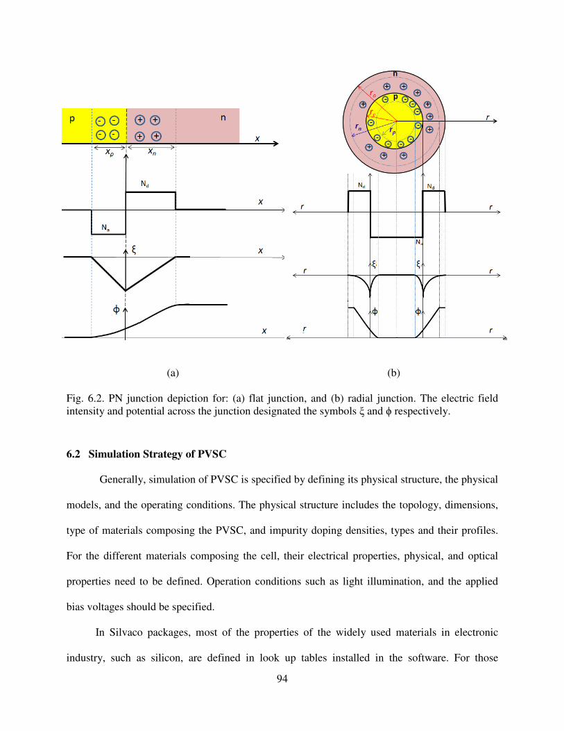
94
(a)
(b)
Fig. 6.2. PN junction depiction for: (a) flat junction, and (b) radial junction. The electric field
intensity and potential across the junction designated the symbols ξ and ϕ respectively.
6.2 Simulation Strategy of PVSC
Generally, simulation of PVSC is specified by defining its physical structure, the physical
models, and the operating conditions. The physical structure includes the topology, dimensions,
type of materials composing the PVSC, and impurity doping densities, types and their profiles.
For the different materials composing the cell, their electrical properties, physical, and optical
properties need to be defined. Operation conditions such as light illumination, and the applied
bias voltages should be specified.
In Silvaco packages, most of the properties of the widely used materials in electronic
industry, such as silicon, are defined in look up tables installed in the software. For those
95
materials that has no installed properties in the software, or for new materials, one can add their
properties manually in the form of look up tables. For example, amorphous silicon (aSi) optical
and physical properties are specified by modifying of the properties of an already defined
material in the package. By this means, the properties of the old material are overridden by the
aSi properties, that we use in this work to define aSi material.
The physical dimensions and the PVSC structure can be build using the DevEdit3D
package, one of the Silvaco TACAD packages. Moreover, the material type, doping density and
profiles, and contact materials can be specified by the user using the DevEdit3D.
PVSC suffer from losses due to many factors that highly degrade the efficiency of PV
cells. The efficiency loss can be attributed to the following main effects [59]: (i) Optical losses
due to reflection, transmission, shading of connector, and parasitic absorption by the ineffective
materials in the cell. (ii) Carrier Recombination losses due to many factors such as material
defects. (iii) Ohmic losses due to the contacts of the cell electrodes (iv) Open circuit and short
circuit (Voc, and Jsc) losses [59]. In order to obtain realistic results out of the numerical
simulation of a PVSC, the losses should be considered by invoking the loss mechanisms in the
numerical solution.
In general, the main parameters that need to be user-specified in numerical simulation of
PVSC can be summarized by the following: 1- Physical dimension and structure configuration
with meshing schemes (space discretization), 2- Composing materials, 3- Doping levels, types,
and profiles, 4- Materials properties: physical, electrical, and optical, 5- Material defects, 6-
Recombination losses mechanisms and models, 6- Illumination source specifications, 7-
Environment conditions: dark, light illumination, and temperature, 8- Biasing voltages.

96
6.2.1 Physical Properties of Materials
Defects in Amorphous Silicon
In the amorphous materials, a large number of defect states occur within the band gap of the
material. In aSi, these defects play significant role in a device operation. To accurately model the
PVSC that contains aSi, the defects density of states (DOS) in aSi should be considered.
Continuous density of defects states is employed in Silvaco (ATLAS) to model the defects in
aSi. This model is installed in the Silvaco (ATLAS) software package, which specifies the DOS
as a combination of exponentially decaying band tail states and Gaussian distributions of mid-
gap states and can be user-activated by “DEFECTS” statement, as demonstrated in Appendix
(C).
Minority Carriers Properties
Another important factor need to be user-specified in the simulation is the minority carrier
lifetime and mobility. For bulk crystalline silicon (cSi), the mobility and the carrier lifetime are
functions of doping levels that can be calculated using the empirical formulas [59]. The bulk
material electrical properties are user specified, where the software considers the other factors
that affect the carriers properties, such as surface recombination and the defects density, to
calculate effective properties [77].
For the aSi, there are typical ranges of these parameters that depends on many factors such as
defects properties in the material and doping levels and temperature [75]. Experimental electrical
properties of high quality aSi, taken from Ref. [78] and [79] are employed in simulations in this
chapter, where the electron and hole mobility are set to be 2 and 0.005 2( / . )cm V s , respectively.
Recombination Loss Models
The recombination is a dominant factor that plays important role in determining PVSC electrical
properties. Therefore, invoking the losses in the simulation is necessary, which can be done in

97
Silvaco (ATLAS) by activating certain loss models in simulation. The recombination losses that
are taken in consideration are the radiative, Shockley-Read-Hall, Auger and surface
recombination. The models of the recombination that are implemented in the SILVACO can be
activated by the user [77].
6.2.2 Photo-generation
The electrodynamic field inside the PVSC structure can be computed in SILVACO (ATLAS) by
using numerical electromagnetic methods such as, FDTD, transfer matrix method (TMM), and
ray tracing methods in Silvco software. Once electromagnetic solution of a structure is obtained,
the resultant intensities of the electric field are exported (interpolated) back onto the device
simulation mesh. These light intensities are used to calculate photo generation rates which are
used directly in the drift-diffusion equations [79], [77].
6.2.3 Light Illumination Source
The standard solar irradiance spectrum, AM1.5G, is used as the optical source that illuminates
the PVSC structures at normal incidence for the optical generation to simulate the J-V
characteristics curve under standard one-sun illumination conditions.
6.3 Numerical Simulation VS Analytical Model
In the approximate mathematical model of the PVSC, different assumptions are invoked to
simplify the analysis. Such models help in understanding the behavior of the solar cells. To make
a proposed PVSC model more meaningful, many aspects need to be considered such as, the NW
topology, doping densities and profiles, light intensity distribution, photo-generation rates,
recombination losses, and surface recombination. All of these factors render analytical models
quite complicated, which eventually led to adopt numerical modeling and simulation to handle
all of these coupled physical mechanisms. An assumption that is usually invoked for molding is
that the NW has infinite length, which renders the electric field symmetrical along the axis. In

98
practical, the finite length of the NW renders the electrical field in the radial junction to be
asymmetrical. However, the analytical model is valid for the region far from the top and bottom
ends of the NW.
6.3.1 Partially Depleted Core
To verify the accuracy and validity of the Silvaco simulation results, we use the analytical
solution for a radial junction to calculate the depletion region width, as given in Ref. 67, and
compare it with that of simulation results. For clarity, the simulated radial PN junction NW is
assumed to be cSi, with uniform doping profiles with p-type of doping density of 17 3
5 10 / cm× in
the core, and n-type doping density of 16 3
5 10 / cm× in the shell. The core radius is set to 180
nm, the shell outer radius is set to 400 nm, and the length is set to be 2.3 µm. Figure 6.3 shows
3D schematic of the core-shell NW radial PN junction cell showing both the core and the shell.
The depletion region border radius, nr , shown in Fig. 6.2 can be written as [74]:
2 2 2( )an c c p
d
Nr r r r
N= + − (6.11)
and the build in potential in the radial junction, biV , can be written as [74]:
2 22 2
0 0 2 2
1 1ln( ) ln( )
2 2 2 2 2 2
a p d nbi n p
p p n n
qN r qN rr r r rV
r r r r
= − = + + + + +
φ φ
ε ε (6.12)
Since biV can be found from the relationship
2ln( )a d
bi
i
N NktV
q n= [59], where 25
ktmV
q≈ and
2 20 610 /in cm= at 300 K 0.85bi
V V⇒ ≈ . By substituting Equations (6.11) in Equation (6.12)
and rearranging, we get transcendental equation as:

99
2 2 2
2 2 2
0 0
2 2
( )
( ( ) ) 2ln 14
( ) 2ln 10.85
ac c p
da
bi n p d c c p
d c
p
c a d a p
c
Nr r r
NNqV N r r r
N r
rr N N N r
r
+ −
= − = + − −
+ + + − =
φ φε
(6.13)
By substituting the values of doping levels and the core radius in Equation (6.13) and solving the
transcendental equation, we find that 161pr nm≈ , and from Equation (6.12) that 311n
r nm≈ .
Fig. 6.3. A schematic of radial core-shell PN junction with uniform doping profiles.
Figure 6.4 shows the spatial distribution of the electric field intensity across the radial junction
with color coded field intensity levels.
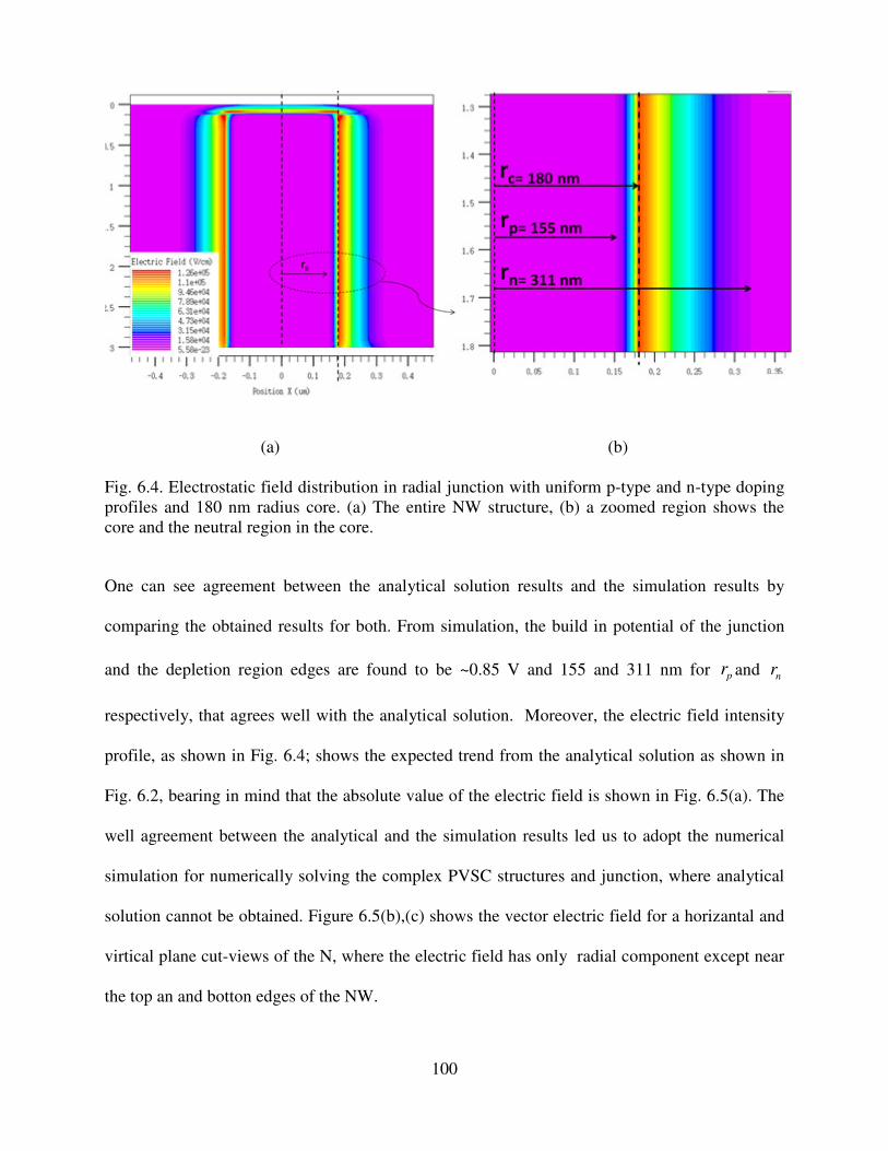
100
(a)
(b)
Fig. 6.4. Electrostatic field distribution in radial junction with uniform p-type and n-type doping
profiles and 180 nm radius core. (a) The entire NW structure, (b) a zoomed region shows the
core and the neutral region in the core.
One can see agreement between the analytical solution results and the simulation results by
comparing the obtained results for both. From simulation, the build in potential of the junction
and the depletion region edges are found to be ~0.85 V and 155 and 311 nm for pr and nr
respectively, that agrees well with the analytical solution. Moreover, the electric field intensity
profile, as shown in Fig. 6.4; shows the expected trend from the analytical solution as shown in
Fig. 6.2, bearing in mind that the absolute value of the electric field is shown in Fig. 6.5(a). The
well agreement between the analytical and the simulation results led us to adopt the numerical
simulation for numerically solving the complex PVSC structures and junction, where analytical
solution cannot be obtained. Figure 6.5(b),(c) shows the vector electric field for a horizantal and
virtical plane cut-views of the N, where the electric field has only radial component except near
the top an and botton edges of the NW.

101
(a)
(b)
(c)
Fig. 6.5. (a)The spatial distribution of the electric field intensity and the profile of the absolute
value of the electric field intensity at horizontal cutline. (b) The vector electrical field horizontal
cut plane near the middle of the cell with color coding the magnitude of vector, and (c) Vertical
cut plane view.

102
6.3.2 Fully and Partially Depleted Radial Junction
In the NW PVSC, there are many competing factors that affect PV device performance such as
radius value. In the previous chapters, we show the effect of the radius value of NW on the
optical properties. Optically, the performance of an array depends on the chosen radius values.
Electrically, the carrier collection efficiency is 100% in the fully depleted region in a PV cell
[59]. Therefore, in the PVSC devices which have very low carrier lifetime, the width of the
depletion regions is targeted to be as wide as possible. In the case of the radial junction NW, a
fully depleted core can degrade the collection efficiency. This can be understood from the
distribution of the build-in electric field in the junction. The width of a depletion region in radial
junction is a function of the radius of the core and the doping densities levels, as Equations
(6.12). To show the effect of radius value on forming the fully or partially depleted core we
conducted numerical simulation for two radial PN junctions. Figure 6.6 shows the electric field
intensity of the radial PN junction for the two examples junction. The doping levels and profiles
for the two examples are kept as in the previous section. One can see that the core NW can be
fully depleted depending on the radius at a given doping level. Figure 6.6 show the electric field
intensity distribution, for vertical cut-plane of the NW radial junction, and absolute value of the
electric field intensity profile for horizontal cutline in the plane. One can see that the 50 nm
radius core is fully depleted. Since the optical properties of a NW array are affected by NW
radius value, the optimal optical performance coupled with fully depleted cores should be
targeted in a design. These are two competing goals, which lead us to adapt the SiNC arrays,
which can offer remarkable optical properties, as have been discussed in Chapter 5 and fully
depleted regions, as we will discuss in this chapter
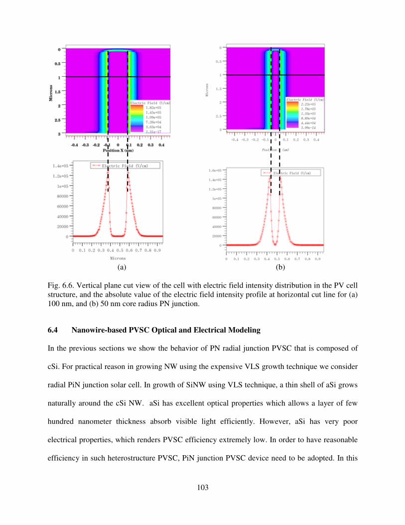
103
(a) (b)
Fig. 6.6. Vertical plane cut view of the cell with electric field intensity distribution in the PV cell
structure, and the absolute value of the electric field intensity profile at horizontal cut line for (a)
100 nm, and (b) 50 nm core radius PN junction.
6.4 Nanowire-based PVSC Optical and Electrical Modeling
In the previous sections we show the behavior of PN radial junction PVSC that is composed of
cSi. For practical reason in growing NW using the expensive VLS growth technique we consider
radial PiN junction solar cell. In growth of SiNW using VLS technique, a thin shell of aSi grows
naturally around the cSi NW. aSi has excellent optical properties which allows a layer of few
hundred nanometer thickness absorb visible light efficiently. However, aSi has very poor
electrical properties, which renders PVSC efficiency extremely low. In order to have reasonable
efficiency in such heterostructure PVSC, PiN junction PVSC device need to be adopted. In this

104
device configuration, the poor electrical properties of the aSi due to fast recombination of the
carriers can be overcome by the build-in electric field across amorphous intrinsic layer, which
allows fast separation and collection of the carriers under the influence of this field. Figure 6.7
shows a schematic of horizontal cut view of radial and flat PiN junction.
(a)
(b)
Fig. 6.7. Vertical cut plane to a flat PiN junction PVSC, and (b) Horizontal cut-plane of radial
PiN PVSC
In this section, we have focused on the optical and electrical properties of PiN radial PVSC
based on core-shell heterostructure of cSi-aSi-Zno. The first subsection shows the optical
properties of PiN junction PVSC that is based on the introduced SiNW array in the previous
chapter. The ultimate goal is to simulate the 3D PiN PVSC that are based on SiNW arrays
under realistic operation conditions with considering all coupled physical mechanisms. In other
words, we aimed to simultaneously solve the Maxwell’s equations and the transport equations of
the 3D structure of the PVSC, this to show the benefits of SiNW array structure and to test its
effect on the electrical device performance. Unfortunately, due to the large computation
requirements and to the limitation in Silvaco software, such full 3D simulation of a PVSC that
based on SiNW array is currently prohibitive. Thus, in the current study we restrict the
simulation on single NW PiN junction PVSC in the second subsection.
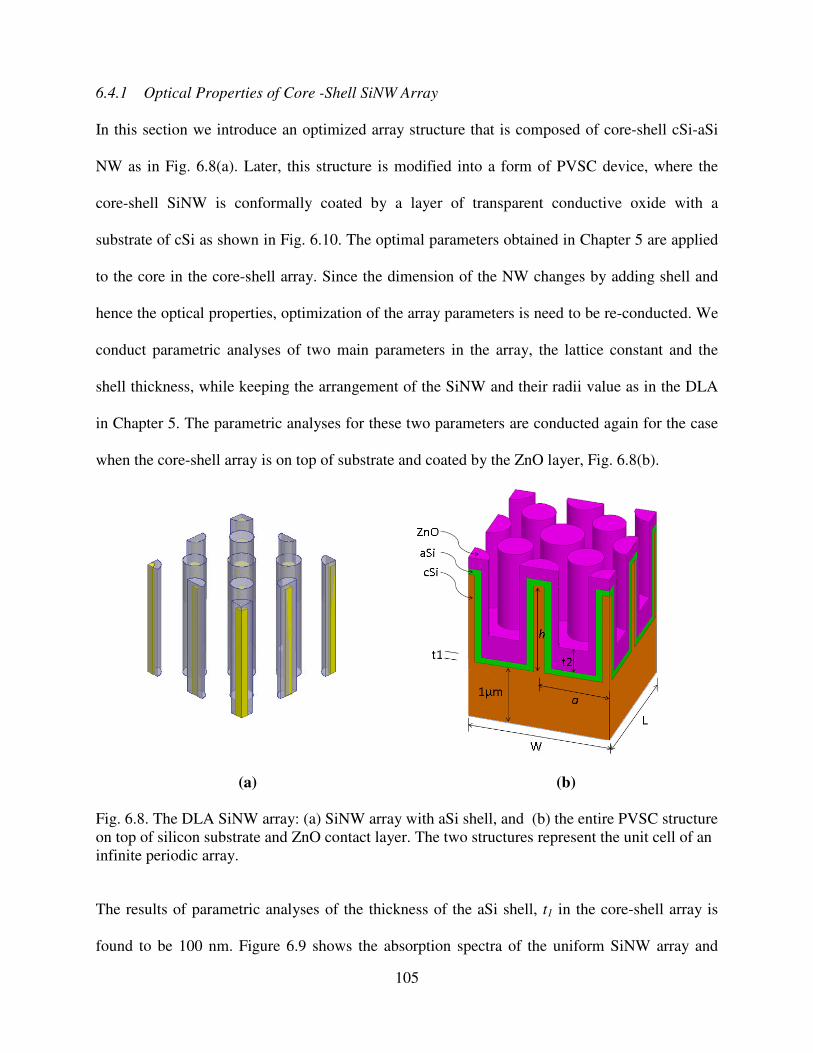
105
6.4.1 Optical Properties of Core -Shell SiNW Array
In this section we introduce an optimized array structure that is composed of core-shell cSi-aSi
NW as in Fig. 6.8(a). Later, this structure is modified into a form of PVSC device, where the
core-shell SiNW is conformally coated by a layer of transparent conductive oxide with a
substrate of cSi as shown in Fig. 6.10. The optimal parameters obtained in Chapter 5 are applied
to the core in the core-shell array. Since the dimension of the NW changes by adding shell and
hence the optical properties, optimization of the array parameters is need to be re-conducted. We
conduct parametric analyses of two main parameters in the array, the lattice constant and the
shell thickness, while keeping the arrangement of the SiNW and their radii value as in the DLA
in Chapter 5. The parametric analyses for these two parameters are conducted again for the case
when the core-shell array is on top of substrate and coated by the ZnO layer, Fig. 6.8(b).
(a)
(b)
Fig. 6.8. The DLA SiNW array: (a) SiNW array with aSi shell, and (b) the entire PVSC structure
on top of silicon substrate and ZnO contact layer. The two structures represent the unit cell of an
infinite periodic array.
The results of parametric analyses of the thickness of the aSi shell, t1 in the core-shell array is
found to be 100 nm. Figure 6.9 shows the absorption spectra of the uniform SiNW array and

106
DLA, where both are covered by conformal 100 nm aSi shell. This absorption spectrum shows
the advantage of employing the DLA configuration in this core-shell structure. In Chapter 5, we
showed that the DLA configuration has intrinsic feature in enhancing the absorption spectrum
over the entire spectrum. In the current core-shell configuration, DLA have the same effect on
enhancing the absorption mainly in the IR band. This can be inferred from Fig. 6.9 where the
uniform core-shell array shows enhanced absorption in both visible and IR bands.
Fig. 6.9. The absorption spectra of DLA array (solid black), and uniform array that are coated by
amorphous silicon layer.
In the radial PiN PVSC configuration, the aSi layer has two main roles, one it functions as a
passivation material for the cSi core surface, and two, it functions as intrinsic layer where most
of the visible light is absorbed. The aSi has strong absorption in visible band, which makes a thin
layer sufficient to absorb large percentage of visible light. In fact, this feature of aSi combined
with array configuration, which reduces the reflection and enhances light trapping in the array
0
0.1
0.2
0.3
0.4
0.5
0.6
0.7
0.8
0.9
1
300 400 500 600 700 800 900 1000
Ab
sorp
tan
ce
Wavelength (nm)
DLA with a-Si shell
Regular array with a-Si sell

107
structure, produce the unique absorption spectrum, as in Fig. 6.9. By this means, the aSi layer
absorbs the visible light and transmit the IR, which is absorbed by the cSi core. Optimization of
the array dimensions and lattice constant are conducted for the ultimate efficiency. The
absorption spectrum of the optimized PiN PVSC device structure is shown in Fig. 6.10. This
verifies that the heterostructure would not degrade the enhanced light trapping performance
obtained by using the DLA configuration. The PVSC, based on the DLA array, is shown in the
inset of Fig. 6.10, with optimum dimensions.
Fig. 6.10. The absorption spectrum of the PVSC structure. The inset shows the three layer
PVSC on top of 1.0 µm thickness substrate.
In PiN PVSC structure, shown in Fig. 6.10, ZnO is employed as n+-type contact layer with
doping density 19 310 / cm . Despite this, in simulations of the PVSC optical properties, we use the
optical properties of the un-doped ZnO, because the doped ZnO shows close optical properties to
0
0.1
0.2
0.3
0.4
0.5
0.6
0.7
0.8
0.9
1
300 400 500 600 700 800 900 1000
Ab
sorp
tan
ce
Wavelength (nm)

108
that of the un-doped [80, 81]. The achieved ultimate efficiency of the optimized PVSC structure,
shown in Fig. 6.10., is of ~39.5%. The estimated maximum short circuit current can be
calculated as [34]:
( ) ( )300
g
sc
nm
eJ I A d
hc= ∫
λλ
λ λ λ (6.19)
which yields a short circuit current density as231 /sc mAJ cm≈ . This estimation is based on the
assumptions that the carrier losses are negligible and the collection efficiency is 100%.
6.4.2 Electrical Properties of PiN Radial Junctions
In the current section we conduct numerical simulation for a single silicon radial PiN junction, as
shown in Fig. 6.1, this is to show the equilibrium solution of the PiN radial junction. The aSi
shell layer plays the role of absorption of the visible light in the range of λ=300-~750 nm, where
few hundreds of nanometer thickness of the aSi shell is sufficient to absorb light efficiently. The
geometry of the NW array, as shown in earlier chapters, plays important role in reducing
reflectance and confines the light in the structure of the array. In addition to the high absorption
coefficient of amorphous silicon, the geometry enhances light trapping and increases total
efficiency. Since the aSi transmits light of wavelengths greater than ~750 nm, the crystalline core
plays important role in utilizing the IR band of the spectrum. The dimensions of the cSi core
radius, aSi shell thickness, and ZnO layer thickness, are selected to be 180, 100, and 200 nm
respectively. As shown in Fig. 6.12, the electric field is radially directed. The generated electrons
and holes in the intrinsic layer are separated and drifted under the influence of the electric field.
For the light absorbed in the cSi core, the generated minority carriers in the quasi neutral region
have large recombination loss rate, especially for high densities of doping.

109
(a) (b)
(c) (d)
Fig. 6.12. (a) Color coded electric field intensity distribution in a horizontal cut-plane of the cell
with electric field intensity as a function radius, and (b) Color coded electric field intensity
distribution in a vertical cut-plane of the cell with electric field intensity as a function radius. The
color coded vectors represents the electric field for (c) horizontal and (d) vertical cut views.

110
The advantage of NW as a light concentrator would be especially degraded by the high
recombination losses of the carriers in the core. The minority carries in the depletion region in
the core have high probability to be collected without being recombined. Figure 6.12 (a, b)
shows the electric field distribution in a PIN radial junction in horizontal and vertical cut views.
It can be seen that the shell is fully depleted, whereas the core is partially depleted. The electric
vector field is shown in Fig. 6.12 (c), where electric field has a single component in the radial
direction. This radially directed electric field can lead to confinement of the carriers inside the
core of the NW with low probability to be collected and high probability to recombine,
especially in fully depleted cores. In other words, since the PiN PVSC device is a drift current
device, the electric field should play the role of drifting the generated carriers toward the contact
electrode to be collected, which does not happen in the case of the radial PiN junction. To
overcome these two competing effects, light absorption efficiency and completely depleted core
that are coupled to the radius value, SiNC is proposed and will be discussed in Section (6.5).
6.5 Geometry Effect on SiNW PVSC Electrical Properties
In the previous chapter, the effect of array geometry on light absorption has been introduced. In
this section we show the effect of geometry on the electrical properties of a radial junction
PVSC. For this, we investigate the SiNC based PVSC. The rationale for investigation NC
geometry in specific is that NC arrays show superior optical performance, which makes them
promising for PV applications, and they can offer enhanced electrical performance.
Unfortunately, 3D simulation of SiNC geometry is computationally prohibitive in the current
version of Silvaco software. To overcome this, we adopted a 3D ridge configuration, as shown in
Fig. 6.13(a), to represent 2D cross section that resembles a cone cross section. By this means,
the obtained solution in the vertical cut plane can be rotated around the axis to produce a 3D

111
cone solution. Nevertheless, in order to make fair comparison, we adopted two ridge
configurations, triangular and rectangular as shown in Fig. 6.13. The PVSC in this manner is a
radial PIN junction cell composed of cSi core, intrinsic layer of aSi, and a contact layer of
Aluminum doped Zinc oxide (Al:ZnO). A substrate of cSi is assumed with Aluminum anode
back contact. The heights of the two ridges are 2.3 µm, and the substrate is set to be 1.0 µm
thick. The width of the bottom of the triangular ridge is set to be 0.5 µm, as well the rectangular
to represent NC and NW of radii of 0.25 µm.
(a)
(b)
Fig. 6.13. Triangular and rectangular ridge shaped PIN cells. (a) Triangular ridge and represents
SiNC cross section (b) rectangular ridge represents SiNW cross section.
Each of the materials composing the current cell has different optical properties and strength of
light absorption. The effective materials in the PV cell are the aSi and cSi. The thin layer of aSi
highly absorbs light in the range of λ=300-~750 nm, and transmits the IR band. The cSi weakly
absorbs IR. Even though, because of the concentration and light trapping property of the SiNW
and SiNC, the core cSi plays a role in utilizing the band that is usually not being utilized by the
aSi PVSC. This concept is demonstrated by the schematic in Fig. 6.14. The generated carriers in
the intrinsic thin layer, under the influence of the junction electric field are drifted to the contact
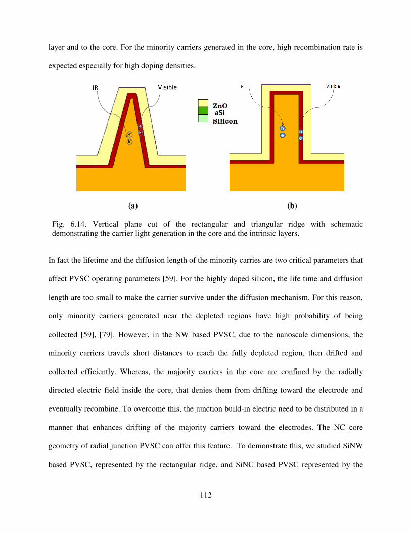
112
layer and to the core. For the minority carriers generated in the core, high recombination rate is
expected especially for high doping densities.
(a)
(b)
Fig. 6.14. Vertical plane cut of the rectangular and triangular ridge with schematic
demonstrating the carrier light generation in the core and the intrinsic layers.
In fact the lifetime and the diffusion length of the minority carries are two critical parameters that
affect PVSC operating parameters [59]. For the highly doped silicon, the life time and diffusion
length are too small to make the carrier survive under the diffusion mechanism. For this reason,
only minority carriers generated near the depleted regions have high probability of being
collected [59], [79]. However, in the NW based PVSC, due to the nanoscale dimensions, the
minority carriers travels short distances to reach the fully depleted region, then drifted and
collected efficiently. Whereas, the majority carriers in the core are confined by the radially
directed electric field inside the core, that denies them from drifting toward the electrode and
eventually recombine. To overcome this, the junction build-in electric need to be distributed in a
manner that enhances drifting of the majority carriers toward the electrodes. The NC core
geometry of radial junction PVSC can offer this feature. To demonstrate this, we studied SiNW
based PVSC, represented by the rectangular ridge, and SiNC based PVSC represented by the

113
triangular ridge. The SiNW based PVSC has symmetrical radial electric field with nearly zero
axial components, the y direction in Fig. 6.15. For typical radius and doping levels, the core is
partially depleted with a thin layer. This is illustrated in Fig. 6.12, and is demonstrated by in the
rectangular ridge that represents a SiNW of radius of 0.25 µm in Fig. 6.15, where the electric
field intensity spatial distribution and profile at different cut lines are shown for equilibrium
solution of the junction. The electric field components, the horizontal and the vertical, are plotted
at three horizontal cut lines as shown in the Fig. 6.14 (a). It can be see that the vertical
component of the field near the top of the core, line 1, has noticeable value compared with the
horizontal.
The SiNC configuration, represented by the triangular ridge in Fig. 6.14(a), exhibits axially
directed electric field component in addition to the radial component. The radial and the axial
components of the electric field profiles are plotted at three cut lines, in the x and y directions in
Fig. 6.16. From the electric field profiles at the different cut lines, we can see that the NC core is
fully depleted down from the top edge to first cut line, where the magnitude of the axial and the
radial electric fields are comparable, Fig. 6.15(b). The presence of the axially directed electric
field component in the build-in electric field enhances the drift of the carriers toward the
electrode, rather than been confined in the core as in the SiNW case.
In fact, the axially directed electric field plays important role in drifting the carriers along the
axis direction toward the contact layer. The electric field intensity profiles in the NC compared
with that of the NW show that the carriers generated in the NC core can have higher probability
to be collected, due to the presence of the axial electric field component. Figure 6.17 shows the
holes current density distribution inside both structures

114
(a)
(b)
(c)
(d)
Fig. 6.15 (a) The electric field intensity distribution in a vertical cut plane of the ridge with the
electric field magnitude at four cut lines plotted in log-scale. The profiles of the electric field at
(b) line 1, (c) line 2, and (d) line 3.
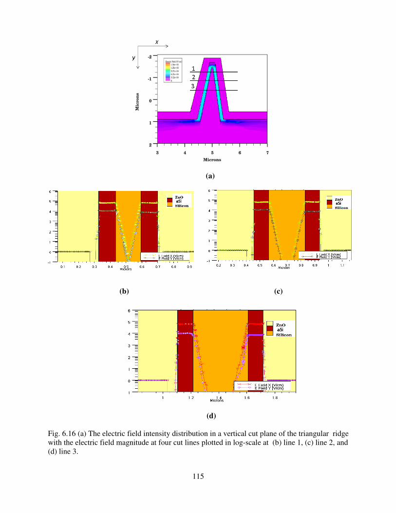
115
(a)
(b)
(c)
(d)
Fig. 6.16 (a) The electric field intensity distribution in a vertical cut plane of the triangular ridge
with the electric field magnitude at four cut lines plotted in log-scale at (b) line 1, (c) line 2, and
(d) line 3.

116
The current density distribution is plotted under the illumination of AM1.5 solar irradiance
spectrum. To make a fair comparison, we assumed homogenous generation rate by invoking ray
tracing optical method. From the current density distribution shown in Fig. 6.17, one can see that
the NC geometry enhances drifting the carriers toward the contact layer.
(a) (b)
Fig. 6.17. The current density distributions for the h in (a) triangular ridge, and (b) rectangular
ridge. The densities are color coded in linear scale.
The I-V characteristics curve of the of the two cell configurations are shown in Fig. 6.18. The
short circuit current of the triangular ridge shows higher value that of the rectangular, and the
open circuit voltage for both shows slight difference. The higher short circuit current density can
be attributed to the better collection of the carriers as a result of the NC geometry. Table 6.2
shows the operating parameters of the two configuration of NW based PVSC. The enahnced
efficincy of the triangular ridge PVSC can be attributed to the enhanced collection efficincy of
the minority carriiers in the core.
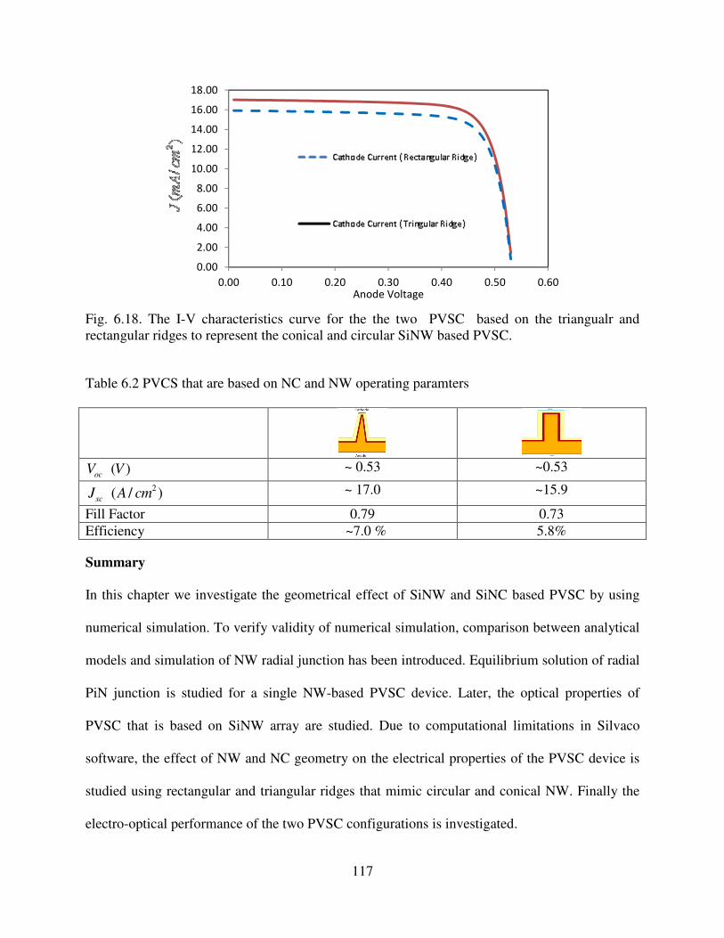
117
Fig. 6.18. The I-V characteristics curve for the the two PVSC based on the triangualr and
rectangular ridges to represent the conical and circular SiNW based PVSC.
Table 6.2 PVCS that are based on NC and NW operating paramters
( )
ocV V ~ 0.53 ~0.53
2( / )scJ A cm ~ 17.0 ~15.9
Fill Factor 0.79 0.73
Efficiency ~7.0 % 5.8%
Summary
In this chapter we investigate the geometrical effect of SiNW and SiNC based PVSC by using
numerical simulation. To verify validity of numerical simulation, comparison between analytical
models and simulation of NW radial junction has been introduced. Equilibrium solution of radial
PiN junction is studied for a single NW-based PVSC device. Later, the optical properties of
PVSC that is based on SiNW array are studied. Due to computational limitations in Silvaco
software, the effect of NW and NC geometry on the electrical properties of the PVSC device is
studied using rectangular and triangular ridges that mimic circular and conical NW. Finally the
electro-optical performance of the two PVSC configurations is investigated.
0.00
2.00
4.00
6.00
8.00
10.00
12.00
14.00
16.00
18.00
0.00 0.10 0.20 0.30 0.40 0.50 0.60Anode Voltage

118
CHAPTER 7
Summary, Conclusions, and Future Work
The study in this dissertation is set out to explore the potentials of SiNW arrays in light
trapping and absorption for high efficiency thin film PVSC applications. Based on this objective,
the study sought to answer the following questions: (i) Have the potentials of SiNW arrays in
light trapping and absorption been reached by the proposed arrays in literature? (ii) What is the
role of geometry in determining the optical properties of SiNW array? And how can we utilize
them for enhancing SiNW arrays performance? (iii) Can a SiNW-based PVSC device achieve
high efficiency? These four questions form the backbone of this dissertation. The following
paragraphs summarize the main answers to the study’s research questions.
First, to explore the potential of SiNW arrays for light absorption, we studied the factors
that can affect the optical properties of SiNW arrays. We found that different geometrical factors
affect the optical properties of uniform SiNW arrays, such as the lattice constant of an array,
lattice configuration, and the radius of NW composing the array. One important factor is the NW
radius, which plays a major role in determining the absorption spectrum of a NW array. We
utilized this fact to introduce SiNW arrays that are composed from NW with radial diversity. The
obtained results showed that enhancing and broadening the absorption of light in SiNW arrays
can be achieved by diversifying the NW radii. By applying diversity of NW radii on an
optimized uniform SiNW array, the light absorption, quantified by the ultimate efficiency of the
array, is enhanced ~ 27 % over the original uniform array, coupled with reduction in the amount
of the used material by ~29%.
Second, the role of three coupled geometrical factors on the absorption spectrum of
diverse NW radii array has been studied. These factors are the radial diversity of SiNW, the
arrangement of these SiNW in a lattice, and the lattice configuration of the array. We found that

119
it is not only the radial diversity of NW that enhances the performance, but also both the
arrangement of the NW and the lattice configuration of an array have significant impact on
enhancing and broadening the absorption spectrum.
Third, taking these findings as basic principles, the next logical step was to introduce
SiNW arrays with optimal lattice configurations and arrangements of the diverse radius SiNW.
Inspired by nature, we introduced two array configurations: the first is the FLA that is inspired
by fractal geometry, and the second is the DLA inspired by the diamond crystal lattice structure.
The introduced SiNW arrays exhibit enhanced optical absorption, especially the DLA which
show strong light absorption that covers the entire solar spectrum of interest, where ultimate
efficiency as high as ~40 % was achieved. In addition, DLA show significant reduction in the
amount of the used material, where filing fraction as low as ~19 % can be achieved. In fact, the
introduced SiNW DLA show near-unity ideal absorption spectrum by using few micrometers
thickness arrays. Such ultimate efficiency is ~ 34% higher than the best reported ultimate
efficiency in the literature for equivalent thickness SiNW arrays and ~185% relative to
equivalent-thickness silicon film. In addition, the proposed DLA arrays attain high ultimate
efficiency for wide angle of light incidence, 70 and 60 degree for parallel and perpendicular
polarizations, respectively.
Finally, we observe that the geometry of a NW-based PVSC has effect on electrical
performance of PVSC device. SiNC-like PVSC device performance is investigated and
compared with rectangular-like PVSC. The efficiency of the SiNC-like PVSC is 7.0%, whereas
it is 5.8% for SiNW-like array. The geometry plays a role in enhancing electrical properties of
PVSC. These two observations, the enhanced optical and electrical performance of SiNC
geometry, leads to the conclusion that a thin film PVSC that is based on the proposed SiNC
arrays can achieve higher efficiency.

120
Conclusions
The achieved strong broadband absorption of light by using the indirect bandgap silicon material
in the form of SiNW arrays is a significant progress toward producing low cost and high
efficiency thin films PVSC. This can establish for new optoelectronics device applications based
on silicon. In addition to the high efficiency thin film PVSC, more sensitive electro optical
sensors and devices can be produced based on SiNW arrays. The proposed SiNW arrays,
configurations, and their design approach can be applied for wide range of applications. For
example, the design procedure can be applied to other semiconductor materials. If applied to
expensive semiconductor materials, this would lead to lower cost and better performance electro-
optical devices due to reduction of the amount of the used material and the enhanced efficiency.
Enhanced efficiency multi-spectral sensors that cover the visible and the IR bands can be
designed based on the introduced NW array configurations, as possible application. Broadband
and wide angular response anti-reflection coating films for optical applications can be produced
based on these design procedures.
Prospects and Future Work
Enhancing light trapping techniques, such as plasmonic light trapping, is a possible application
of SiNW array design concepts used in this work. Extending the design approach in this work to
the microwave band is another possibility, which can lead to design broadband low reflectance
and high absorptance thin layers that can be used as microwave absorptive materials, and in
electromagnetic interference applications.
Despite that the theoretical results and work in this dissertation presents a self-contained piece of
work that led to publication of four journal and conference papers, the following future works are
recommended based on the results of this research:

121
1- Because of the multiple competing parameters in the SiNW arrays and the PVSC,
heuristic optimization techniques such as genetic algorithms would be possible future work to
optimize and design NW arrays and PVSC devices.
2- 3D simulation of NW array-based PVSC device using Silvaco packages, which can be
performed by utilizing more robust computational techniques, such as distributed computation
techniques by using high performance computing.
3- Applying the proposed concepts of design to other semiconductor NW arrays and other
light trapping technique.
4- Realization of the proposed SiNW arrays and conduction of experimental measurements
of their optical properties.
.

122
References
[1] W. Xu, “Silicon Nanowire Anode for Lithium-Ion Batteries: Fabrication, Characterization
and Solid Electrolyte Interphase,” Louisiana State University, 2011.
[2] “International Energy Outlook 2014 - Energy Information Administration.” [Online].
Available: http://www.eia.gov/forecasts/ieo/. [Accessed: 15-May-2015].
[3] O. Morton, “Solar energy: A new day dawning?: Silicon Valley sunrise,” Nature, vol. 443,
no. 7107, pp. 19–22, Sep. 2006.
[4] B. Hua, Q. Lin, Q. Zhang, and Z. Fan, “Efficient photon management with nanostructures for
photovoltaics,” Nanoscale, vol. 5, no. 15, pp. 6627–6640, Jul. 2013.
[5] P. Spinelli, V. E. Ferry, J. van de Groep, M. van Lare, M. A. Verschuuren, R. E. I. Schropp,
H. A. Atwater, and A. Polman, “Plasmonic light trapping in thin-film Si solar cells,” J. Opt.,
vol. 14, no. 2, p. 024002, Feb. 2012.
[6] H.-P. Wang, D.-H. Lien, M.-L. Tsai, C.-A. Lin, H.-C. Chang, K.-Y. Lai, and J.-H. He,
“Photon management in nanostructured solar cells,” J. Mater. Chem. C, vol. 2, no. 17, pp.
3144–3171, Apr. 2014.
[7] C. H. Lee, D. R. Kim, I. S. Cho, N. William, Q. Wang, and X. Zheng, “Peel-and-Stick:
Fabricating Thin Film Solar Cell on Universal Substrates,” Sci. Rep., vol. 2, Dec. 2012.
[8] Q. G. Du, C. H. Kam, H. V. Demir, H. Y. Yu, and X. W. Sun, “Broadband absorption
enhancement in randomly positioned silicon nanowire arrays for solar cell applications,”
Opt. Lett., vol. 36, no. 10, pp. 1884–1886, May 2011.
[9] N. Huang, C. Lin, and M. L. Povinelli, “Broadband absorption of semiconductor nanowire
arrays for photovoltaic applications,” J. Opt., vol. 14, no. 2, p. 024004, Feb. 2012.
[10]F. Khan, S.-H. Baek, and J. H. Kim, “Dependence of Performance of Si Nanowire Solar
Cells on Geometry of the Nanowires,” Sci. World J., vol. 2014, p. e358408, Jan. 2014.
[11]N. Anttu and H. Q. Xu, “Efficient light management in vertical nanowire arrays for
photovoltaics,” Opt. Express, vol. 21, no. S3, pp. A558–A575, May 2013.
[12]E. Garnett and P. Yang, “Light Trapping in Silicon Nanowire Solar Cells,” Nano Lett., vol.
10, no. 3, pp. 1082–1087, Mar. 2010.
[13]H. Bao and X. Ruan, “Optical absorption enhancement in disordered vertical silicon
nanowire arrays for photovoltaic applications,” Opt. Lett., vol. 35, no. 20, pp. 3378–3380,
Oct. 2010.
[14]L. Tsakalakos, J. Balch, J. Fronheiser, B. A. Korevaar, O. Sulima, and J. Rand, “Silicon
nanowire solar cells,” Appl. Phys. Lett., vol. 91, no. 23, p. 233117, Dec. 2007.

123
[15]B. C. P. Sturmberg, K. B. Dossou, L. C. Botten, A. A. Asatryan, C. G. Poulton, R. C.
McPhedran, and C. M. de Sterke, “Nanowire array photovoltaics: Radial disorder versus
design for optimal efficiency,” Appl. Phys. Lett., vol. 101, no. 17, p. 173902, Oct. 2012.
[16]P. Servati, A. Colli, S. Hofmann, Y. Q. Fu, P. Beecher, Z. A. K. Durrani, A. C. Ferrari, A. J.
Flewitt, J. Robertson, and W. I. Milne, “Scalable silicon nanowire photodetectors,” Phys. E
Low-Dimens. Syst. Nanostructures, vol. 38, no. 1–2, pp. 64–66, Apr. 2007.
[17]T.-T. Xu, J.-A. Huang, L. He, Y. He, S. Su, and S.-T. Lee, “Ordered silicon nanocones
arrays for label-free DNA quantitative analysis by surface-enhanced Raman spectroscopy,”
Appl. Phys. Lett., vol. 99, no. 15, pp. 153116–153116–3, Oct. 2011.
[18]K. J. Morton, G. Nieberg, S. Bai, and S. Y. Chou, “Wafer-scale patterning of sub-40 nm
diameter and high aspect ratio (>50:1) silicon pillar arrays by nanoimprint and etching,”
Nanotechnology, vol. 19, no. 34, p. 345301, Aug. 2008.
[19]H. J. Fan, P. Werner, and M. Zacharias, “Semiconductor nanowires: from self-organization
to patterned growth,” Small Weinh. Bergstr. Ger., vol. 2, no. 6, pp. 700–717, Jun. 2006.
[20]G. Grzela and J. Gómez Rivas (Promotor), A. Polman (Co-promotor), “Directional light
emission and absorption by semiconductor nanowires,” 2013.
[21]K. Tomioka, P. Mohan, J. Noborisaka, S. Hara, J. Motohisa, and T. Fukui, “Growth of
highly uniform InAs nanowire arrays by selective-area MOVPE,” J. Cryst. Growth, vol. 298,
pp. 644–647, Jan. 2007.
[22]J.-P. P. Kakko, T. Haggrén, V. Dhaka, T. Huhtio, A. Peltonen, H. Jiang, E. Kauppinen, and
H. Lipsanen, “Fabrication of Dual-Type Nanowire Arrays on a Single Substrate,” Nano Lett.,
vol. 15, no. 3, pp. 1679–1683, Mar. 2015.
[23]E. J. W. Berenschot, H. V. Jansen, and N. R. Tas, “Fabrication of 3D fractal structures using
nanoscale anisotropic etching of single crystalline silicon,” J. Micromechanics
Microengineering, vol. 23, no. 5, p. 055024, May 2013.
[24]N. Singh, K. D. Buddharaju, S. K. Manhas, A. Agarwal, S. C. Rustagi, G. Q. Lo, N.
Balasubramanian, and D.-L. Kwong, “Si, SiGe Nanowire Devices by Top #x2013;Down
Technology and Their Applications,” IEEE Trans. Electron Devices, vol. 55, no. 11, pp.
3107–3118, Nov. 2008.
[25]W. Zhou, Nanoimprint Lithography: An Enabling Process for Nanofabrication. Springer
Science & Business Media, 2013.
[27]C.-W. Kuo, J.-Y. Shiu, P. Chen, and G. A. Somorjai, “Fabrication of Size-Tunable Large-
Area Periodic Silicon Nanopillar Arrays with Sub-10-nm Resolution,” J. Phys. Chem. B, vol.
107, no. 37, pp. 9950–9953, Sep. 2003.
[28]S. H. Ko, I. Park, H. Pan, C. P. Grigoropoulos, A. P. Pisano, C. K. Luscombe, and J. M. J.
Fréchet, “Direct Nanoimprinting of Metal Nanoparticles for Nanoscale Electronics
Fabrication,” Nano Lett., vol. 7, no. 7, pp. 1869–1877, Jul. 2007.

124
[29]N. C. Lindquist, P. Nagpal, K. M. McPeak, D. J. Norris, and S.-H. Oh, “Engineering metallic
nanostructures for plasmonics and nanophotonics,” Rep. Prog. Phys., vol. 75, no. 3, p.
036501, Mar. 2012.
[30]E. D. Palik, Handbook of Optical Constants of Solids. New York: Academic.
[31]R. Ren, Y.-X. Guo, and R.-H. Zhu, “Enhanced absorption in elliptical silicon nanowire
arrays for solar energy harvesting,” Opt. Eng., vol. 53, no. 2, pp. 027102–027102, 2014.
[32]B. C. P. Sturmberg, K. B. Dossou, L. C. Botten, A. A. Asatryan, C. G. Poulton, C. M. de
Sterke, and R. C. McPhedran, “Modal analysis of enhanced absorption in silicon nanowire
arrays,” Opt. Express, vol. 19, no. S5, pp. A1067–A1081, Sep. 2011.
[33]C. Lin and M. L. Povinelli, “Optimal design of aperiodic, vertical silicon nanowire structures
for photovoltaics,” Opt. Express, vol. 19, no. S5, pp. A1148–A1154, Sep. 2011.
[34]C. Lin and M. L. Povinelli, “Optical absorption enhancement in silicon nanowire arrays with
a large lattice constant for photovoltaic applications,” Opt. Express, vol. 17, no. 22, pp.
19371–19381, Oct. 2009.
[35]K. T. Fountaine, W. S. Whitney, and H. A. Atwater, “Resonant absorption in semiconductor
nanowires and nanowire arrays: Relating leaky waveguide modes to Bloch photonic crystal
modes,” J. Appl. Phys., vol. 116, no. 15, pp. 153106–153106–6, Oct. 2014.
[36]Y. Yu and L. Cao, “Coupled leaky mode theory for light absorption in 2D, 1D, and 0D
semiconductor nanostructures,” Opt. Express, vol. 20, no. 13, pp. 13847–13856, Jun. 2012.
[37]M. Khorasaninejad, N. Abedzadeh, J. Walia, S. Patchett, and S. S. Saini, “Color Matrix
Refractive Index Sensors Using Coupled Vertical Silicon Nanowire Arrays,” Nano Lett., vol.
12, no. 8, pp. 4228–4234, Aug. 2012.
[38]L. Hu and G. Chen, “Analysis of Optical Absorption in Silicon Nanowire Arrays for
Photovoltaic Applications,” Nano Lett., vol. 7, no. 11, pp. 3249–3252, Nov. 2007.
[39]M. Khorasaninejad, N. Abedzadeh, A. S. Jawanda, N. O, M. P. Anantram, and S. S. Saini,
“Bunching characteristics of silicon nanowire arrays,” J. Appl. Phys., vol. 111, no. 4, p.
044328, Feb. 2012.
[40]M. Foldyna, L. Yu, S. Misra, and P. R. i C. Roca i Cabarrocas, “Using nanowires to enhance
light trapping in solar cells,” SPIE Newsroom, Nov. 2013.
[41]S. Patchett, M. Khorasaninejad, N. O, and S. S. Saini, “Effective index approximation for
ordered silicon nanowire arrays,” J. Opt. Soc. Am. B, vol. 30, no. 2, pp. 306–313, Feb. 2013.
[42]J. Li, H. Yu, S. M. Wong, X. Li, G. Zhang, P. G.-Q. Lo, and D.-L. Kwong, “Design
guidelines of periodic Si nanowire arrays for solar cell application,” Appl. Phys. Lett., vol.
95, no. 24, p. 243113, Dec. 2009.

125
[43]Y. Zeng, Q. Ye, and W. Shen, “Design principles for single standing nanowire solar cells:
going beyond the planar efficiency limits,” Sci. Rep., vol. 4, May 2014.
[44]S.-F. Leung, Q. Zhang, F. Xiu, D. Yu, J. C. Ho, D. Li, and Z. Fan, “Light Management with
Nanostructures for Optoelectronic Devices,” J. Phys. Chem. Lett., vol. 5, no. 8, pp. 1479–
1495, Apr. 2014.
[45]E. C. Garnett, M. L. Brongersma, Y. Cui, and M. D. McGehee, “Nanowire Solar Cells,”
Annu. Rev. Mater. Res., vol. 41, no. 1, pp. 269–295, 2011.
[46]L. Cao, P. Fan, and M. L. Brongersma, “Optical Coupling of Deep-Subwavelength
Semiconductor Nanowires,” Nano Lett., vol. 11, no. 4, pp. 1463–1468, Apr. 2011.
[47]R. G. Hunsperger, Integrated Optics: Theory and Technology. Springer Science & Business
Media, 2009.
[48]C. DeCusatis and C. J. S. DeCusatis, Fiber Optic Essentials. Academic Press, 2010.
[49]A. W. Snyder and J. D. Love, Optical Waveguide Theory. Chapman & Hall, 1995.
[50]L. Cao, J.-S. Park, P. Fan, B. Clemens, and M. L. Brongersma, “Resonant Germanium
Nanoantenna Photodetectors,” Nano Lett., vol. 10, no. 4, pp. 1229–1233, Apr. 2010.
[51]G. Gouesbet and G. Gréhan, Generalized Lorenz-Mie Theories. Springer Science & Business
Media, 2011.
[52]W. Hergert and T. Wriedt, The Mie Theory: Basics and Applications. Springer, 2012.
[53]G. Grzela, D. Hourlier, and J. G. Rivas, “Polarization-dependent light extinction in
ensembles of polydisperse, vertical semiconductor nanowires: A Mie scattering effective
medium,” Phys. Rev. B, vol. 86, no. 4, Jul. 2012.
[54]L. Cao, “Optical resonances of semiconductor nanowires Narrow-band analyzer,” Ph.D.
dissertation, Department of Materials Science and Engineering., Stanford Univ., CA,2010.
[55]C. A. Balanis, Advanced Engineering Electromagnetics. John Wiley & Sons, 2012.
[56]D. M. Pozar, Microwave Engineering. Wiley, 1997.
[57]P. P. Altermatt, Y. Yang, T. Langer, A. Schenk, and R. Brendel, “Simulation of optical
properties of Si wire cells,” in 2009 34th IEEE Photovoltaic Specialists Conference (PVSC),
2009, pp. 000972–000977.
[58]Q. G. Du, C. H. Kam, H. V. Demir, H. Y. Yu, and X. W. Sun, “Broadband absorption
enhancement in randomly positioned silicon nanowire arrays for solar cell applications,”
Opt. Lett., vol. 36, no. 10, pp. 1884–1886, May 2011.
[59]M. A. Green, Solar Cells: Operating Principles, Technology, and System Applications.
Englewood Cliffs, NJ: Prentice Hall, 1981.

126
[60]“Solar Spectral Irradiance: Air Mass 1.5.” [Online]. Available:
http://rredc.nrel.gov/solar/spectra/am1.5/. [Accessed: 25-Jun-2015].
[61]Y. Zeng, Q. Ye, and W. Shen, “Design principles for single standing nanowire solar cells:
going beyond the planar efficiency limits,” Sci. Rep., vol. 4, May 2014.
[62]G. Williams, Linear Algebra with Applications, Alternate Edition. Jones & Bartlett Learning,
2011.
[63]B. B. Mandelbrot, The Fractal Geometry of Nature, 1 edition. San Francisco: W. H.
Freeman and Company, 1982.
[64] S.-K. Eah, “A very large two-dimensional superlattice domain of monodisperse gold
nanoparticles by self-assembly,” J. Mater. Chem., vol. 21, no. 42, pp. 16866–16868, Oct.
2011.
[65]L. Anghinolfi, Self-Organized Arrays of Gold Nanoparticles: Morphology and Plasmonic
Properties. Springer Science & Business Media, 2012.
[66]K.-H. Jung, J.-S. Chang, and Y.-S. Kwon, “Two Dimensional Gold Nanodot Arrays
Prepared by Using Self-Organized Nanostructure,” J. Electr. Eng. Technol., vol. 1, no. 2, pp.
246–250, Jun. 2006.
[67]O. H. Alzoubi, H. Abu-Safe, K. Alshurman, and H. A. Naseem, “Broadband Absorptance
High Efficiency Silicon Nanowire Fractal Arrays for Photovoltaic Applications,” in
Symposium UU – Semiconductor Nanowires—Synthesis, Properties and Applications, 2014,
vol. 1707.
[68]O. H. A. Zoubi, T. M. Said, M. A. Alher, S. E. Ghazaly, and H. Naseem, “Broadband high
efficiency silicon nanowire arrays with radial diversity within diamond-like geometrical
distribution for photovoltaic applications,” Opt. Express, vol. 23, no. 15, p. A767, Jul. 2015.
[69]O. H. Alzoubi and H. Naseem, “Broad band absorption silicon nanowire array using diverse
radii for photovoltaic applications,” in Photovoltaic Specialist Conference (PVSC), 2014
IEEE 40th, 2014, pp. 2197–2201.
[70]K. T. Fountaine, W. S. Whitney, and H. A. Atwater, “Resonant absorption in semiconductor
nanowires and nanowire arrays: Relating leaky waveguide modes to Bloch photonic crystal
modes,” J. Appl. Phys., vol. 116, no. 15, p. 153106, Oct. 2014.
[71]N. M. Ali, N. K. Allam, A. M. A. Haleem, and N. H. Rafat, “Analytical modeling of the
radial pn junction nanowire solar cells,” J. Appl. Phys., vol. 116, no. 2, p. 024308, Jul. 2014.
[72] M. M. Adachi, M. P. Anantram, and K. S. Karim, “Core-shell silicon nanowire solar
cells,” Sci. Rep., vol. 3, Mar. 2013.
[73]E. C. Garnett and P. Yang, “Silicon Nanowire Radial p−n Junction Solar Cells,” J. Am.
Chem. Soc., vol. 130, no. 29, pp. 9224–9225, Jul. 2008.

127
[74]A. C. E. Chia and R. R. LaPierre, “Electrostatic model of radial pn junction nanowires,” J.
Appl. Phys., vol. 114, no. 7, p. 074317, Aug. 2013.
[75]Y. Zhan, X. Li, and Y. Li, “Numerical Simulation of Light-Trapping and Photoelectric
Conversion in Single Nanowire Silicon Solar Cells,” IEEE J. Sel. Top. Quantum Electron.,
vol. 19, no. 5, pp. 1–8, Sep. 2013.
[76]B. M. Kayes, H. A. Atwater, and N. S. Lewis, “Comparison of the device physics principles
of planar and radial p-n junction nanorod solar cells,” J. Appl. Phys., vol. 97, no. 11, p.
114302, Jun. 2005.
[77]“Silvaco Support - Download User Manuals.” [Online]. Available:
https://dynamic.silvaco.com/dynamicweb/jsp/downloads/DownloadManualsAction.do?req=s
ilen-manuals&nm=atlas. [Accessed: 24-Jun-2015].
[78]R. Street, Technology and Applications of Amorphous Silicon. Springer Science & Business
Media, 2013.
[79]R. E. I. Schropp and M. Zeman, Amorphous and Microcrystalline Silicon Solar Cells:
Modeling, Materials and Device Technology, 1998 edition. Boston: Springer, 1998.
[80]M. Mazilu, N. Tigau, and V. Musat, “Optical properties of undoped and Al-doped ZnO
nanostructures grown from aqueous solution on glass substrate,” Opt. Mater., vol. 34, no. 11,
pp. 1833–1838, Sep. 2012.
[81]Z. B. Ayadi, L. E. Mir, K. Djessas, and S. Alaya, “Electrical and optical properties of
aluminum-doped zinc oxide sputtered from an aerogel nanopowder target,” Nanotechnology,
vol. 18, no. 44, p. 445702, Nov. 2007.
[82]C. Yeh and F. Shimabukuro, The Essence of Dielectric Waveguides. Springer Science &
Business Media, 2008.
[83]Y. Yu and L. Cao, “Leaky Mode Engineering: A General Design Principle for Dielectric
Optical Antenna Solar Absorbers,” ArXiv13055969 Cond-Mat Physicsphysics, May 2013.
[84]L. F. Chen, C. K. Ong, C. P. Neo, V. V. Varadan, and V. K. Varadan, Microwave
Electronics: Measurement and Materials Characterization. Wiley, 2004.
[85]C. T. A. Johnk, Engineering Electromagnetic Fields and Waves, 2 edition. New York:
Wiley, 1988.
[86]M. A. Khorrami, “Multi-Physics Modeling of Terahertz and Millimeter-Wave Devices,”
Ph.D., University of Arkansas, United States -- Arkansas, 2014.
[87]M. Kemp, M. Meunier, and C. G. Tannous, “Simulation of the amorphous silicon static
induction transistor,” Solid-State Electron., vol. 32, no. 2, pp. 149–157, Feb. 1989.

128
[88]M. Hack, J. G. Shaw, P. G. LeComber, and M. Willums, “Numerical Simulations of
Amorphous and Polycrystalline Silicon Thin-Film Transistors,” Jpn. J. Appl. Phys., vol. 29,
no. 12A, p. L2360, Dec. 1990.
[89]A. Luque and S. Hegedus, Handbook of Photovoltaic Science and Engineering. John Wiley
& Sons, 2011.

129
Appendices
Appendix A: Leaky Wave Guide Mode Analyses
In the following section we show the basic theoretical formulation of the optical fiber and the
leaky mode waveguide, which can be found in different fiber optics and advanced
electromagnetics books [48, 55, 82].
Fig. 2.17 . Dielectric Circular Cylinder waveguide in the cylindrical coordinates system
in
out
n r R inside the cylindern
n r R outside the cylider
<=
> (A.1)
Three assumptions are made in deriving this solution: (i) infinite length circular cylinder, (ii)
lossless dielectric material, and (iii) the dielectric material is non dispersive material. In general
the electric and magnetic fields is represented by cylindrical coordinate as:
( ) ( ) ( )ˆˆ ˆr zE E r E E z= + +
�
ϕ ϕ (A.2)
( ) ( ) ( )ˆˆ ˆr z
H H r H H z= + +�
ϕ ϕ (A.3)

130
The general Helmholtz equation can be written in the form of cylindrical coordinates as:
( )
2 2 2 2
2 2
2 2
2 2
2 2
2ˆ( ) ( )
2ˆ( )
ˆ( ) 0
ro r o r
ro
z o z
E EE n k E E n k E r
r r
EEE n k E
r r
E n k E z
∂ ∇ + = ∇ − − +
∂
∂+ ∇ − − +
∂
+ ∇ + =
� �
ϕ
ϕ
ϕ ϕ
ϕ
ϕϕ (A.4)
Since the equations for r
E and Eϕ
are coupled, we first solve forz
E , where Hz has the solution of
the same Helmholtz equation. Then, other field components can be found from �� and��. Since
all components of the electric and magnetic fields can expresses by ��and �� fields, the solution
of the z
E by using the separation of variables method is as:
�� = (�)�(�)�(�) (A.5)
�(�) = � �!"� + $ �!"� (A.6)
�(�) = % �!&' + ( �!&' (A.7)
(�) = )&(*�) + +,&(*�) (A.8)
Where κ the transverse is wave vector, and defined as:
2 2 2
( )inkn= −κ β (A.9)
and - = 0.1.2… , )&(*�) is the Bessel function of the first kind and νth order, ,&(*�) is the
Bessel function of the second kind and νth order, and (a, b, c, d, e, and f) are constants. The
solution need to be found in two regions, inside and outside the waveguide. Since ,&(*�) has
infinite value at r=0, f is considered zero. Because the solution is obtained for forward
propagating wave, the constants b and c are considered zero also. These yield solution as:
Inside the waveguide (r<R) as:
�� = 3)&(*�) �!&' �!"� + %4�56��6 (A.10)

131
�� = 7)&(*�) �!&' �!"� + %4�56��6 (A.11)
And outside of the waveguide (r> R) as:
�� = 89&(:�) �!&' �!"� + %4�56��6 (A.12)
�� = ;9&(:�) �!&' �!"� + %4�56��6 (A.13)
)& is the Bessel function of the first kind of the -th order, 9& is the modified Bessel of the
second kind of the -th order, γ is the wave vector outside the NW and is defined as :
2 2 2( )
outkn− = −γ β (A.14)
A, B, C, and D are constants. The remaining components of the electric and magnetic fields can
be found in term of ��and �� as [55]:
2
z zr
E HjE
q r r
∂ ∂= − +
∂ ∂
µωβ
ϕ (A.15)
2
z zE Hj
Eq r r
∂ ∂= − −
∂ ∂ ϕ
βµω
ϕ(A.16)
2
z zr
H EjH
q r r
∂ ∂= − −
∂ ∂
ωεβ
ϕ(A.17)
2
z zH Ej
Hq r r
∂ ∂= − +
∂ ∂ ϕ
βωε
ϕ(A.18)
where q2 = ω2µε - β
2 = k
2 - β
2. By applying boundary conditions of electric and magnetic field at
the wall of the cylinder (continuity of the tangential field components zE , Eϕ , z
H , and Hϕ ), a
characteristic equation for a circular optical waveguide can be found in many references and
written as [48], [55], [82]:
( )( )
( )( )
( ) ( )( )
( ) ( )( )
2 2 2' ' ' '2 20 0
2 2 2
1 1
in outJ R K R n k J R n k K R
J R K R J R KR R
+ = + × +
ν ν ν ν
ν ν ν ν
κ γ κ γβ ν
κ γ κ κ γ γ κ κ γ γ (A.19)

132
where R in this case, is the radius of the waveguide, and “'” represents the first derivative of the
Bessel’s function. To find the radial resonance modes, equate the left hand side of the equation to
zero, due to setting axial propagation constant, β , to zero[82].This lead to the characteristic
equation of two parts as:
( )( )
( ) ( ) ( )( )
( ) ( )( )
2 2' ' ' '
0 0 0
in outJ R K R n k J R n k K R
J R K R J R K R
+ + =
ν ν ν ν
ν ν ν ν
κ γ κ γ
κ κ γ κ κ γ γ (A.20)
Solving for the left hand side of this equation leads to the TE modes, and the right hand side
leads to the TM modes. The equations represent the circular symmetry cases are when 0=ν ,
where only TE or TM wave can satisfy boundary conditions[82]. The hybrid modes vm
EH and
vmHE , where 0≠ν , are required to satisfy boundary conditions[82]. Table 2.1 below shows the
cut off modes conditions that can be applied to calculate the modes[82].
Table A.1 Dielectric wave guide cut off modes
Mode Cutoff conditions [82]
0mTE ( )
( )( )( )
' '
0
J R K R
J R K R
+ =
ν ν
ν ν
κ γ
κ κ γ γ, cut off can be found by setting ( )0J Rκ =0
0mTM ( ) ( )
( )( ) ( )
( )
2 2' '
0 0
in outn k J R n k K R
J R K R
+
ν ν
ν ν
κ γ
κ κ γ γ, cut off can be found by setting
( )0J Rκ =0
1mEH
1mHE
cut off can be found by setting ( )1 0J R =κ
vmHE
2≥ν ( ) ( )2
121
1
out
in
n RJ R J R
n−
+ =
− ν ν
κκ κ
ν
vmEH
2≥ν
( ) 0J R =ν κ
The dielectric wave guide can operate as wave guide or a leaky wave guide depending on certain
conditions[83]. If ( 20<γ and 0>κ ), the dielectric waveguide rod behaves as a waveguide. In

133
other word, the waves are confined inside the waveguide. Otherwise, If 20>γ , then it behaves as
leaky waveguide, where the field are not confined inside the waveguide [55],[54]. For dielectric
wave guide with radius less than free space wave, fields of the resonance modes are not
completely confined inside the physical dimensions [54]. The field outside the waveguide decays
evanescently in the radius direction, which can be inferred from the outside region solution in
Equation (A.12). Under certain conditions, leaky wave guide behaves as antenna, and rather than
having evanescent field outside its physical dimensions, these fields radiate[55]. For the leaky
guided modes, the argument of Equation (2.3), ( )Rγ , should be real value. Therefore, ( )Rκ
should fulfill the condition of2
1o coren< −γ β . Otherwise the argument becomes imaginary and
the second order Bessel function reduces to second kind Hankel’s function, which represents un-
attenuated outwardly traveling waves. Under this condition, the dielectric wave guide behaves as
optical antenna because of radiative energy loss from its side [55]. In the leaky waveguide, the
superposition of hybrid modes form linearly what is called linear polarized (LP) modes [82],
[49]. Table A.2 summarizes these LP modes, where the labeling roles for LP modes are as [82],
[55]:
0 1LP HE=µ µ (A.21)
1 2 0 2 0LP HE TE HE TM= + + +µ µ µ µ µ (A.22)
1 2 0 2 0LP HE TE HE TM= + + +µ µ µ µ µ (A.23)
1 1m m mLP HE EH+ −= +µ µ µ (A.24)

134
Table A.2- designation rules for LP modes[82]
mµ 01 11 21 02
mLP µ designation 01LP 11LP 21LP 02LP
Hybrid mode designation 11HE 21HE
01TE
01TM
31HE
11EH
12HE
The electric field density patterns of different LP modes of leaky dielectric waveguide are shown
in Table. A.3
Table A.3- Normalized electric field patterns for the LP modes
µ=1 µ=2 µ=3 µ=4
m=0
m=1
m=2
m=3
m=4

135
Appendix B: Scattering Matrix Method
The finite element method is used to solve Maxwell equations in the array structures in this
study. Then the scattering matrix method, found in different electromagnetic wave references
[56], [84], [85], is utilized to calculate the reflectance, transmittance and absorptance of the
structures.
Fig. B.1 Depiction of semi-infinite dielectric slab with 2n refractive index, k wave vector
inside the material, and thickness of l . The slab is bounded by air in the right and the left sides
and the r and t represents the reflection and transmission coefficients at the air-slab interface.
Fig. B.1 represents a depiction of incident, reflected and transmitted wave through a homogenous
semi-infinite dielectric slab. The incident field is from the left medium with refractive index of
1n , and thus, in medium to the right of the slab is only a forward with refractive index of 2n .In
Fig. B.1, r and t represent the reflection and transmission coefficient at the interface of the
material and air. The reflection and transmission response of the slab under illumination can be
expressed as 11S and
21S , representing the reflection and transmission coefficient of the slab, that
can be defined as 111
1
ES
E
+
−
= and '
221
1
ES
E
+
+
= , where the electric fields are related to each other as:

136
'
1 1 1
'1 11 1
11
1
E r E
E rt E
+ +
− −
=
(B.1)
'
2 2 1
'2 22 1
11
1
E r E
E rt E
+ +
− −
=
(B.2)
The fields '
1E + and '
1E − can be written in terms of 2E + and 2E − as:
'
1 2
'21
0
0
jkl
jkl
E Ee
EE e
+ +
−−−
=
(B.3)
The overall transmission and reflection response of the slab can be written by using the
transform matrices as:
1 1 2
1 1 21
'1 2 2
1 21 2
1 01
1 00
1 101 1
1 1 00
jkl
jkl
jkl
jkl
E r Ee
E r Et e
r re E
r rt te
+ +
− −
+
−
=
=
=
(B.4)
Based on these equations, the transmitted and the reflected fields from the slab, 11S and
21S , can
be written as:
2
1 1 211 2
1 1 21
jkl
jkl
E r r eS
E r r e
−
+
−−
+= =
+ (B.5)
'22
21 2
1 1 21
jkl
t
kl
t t eES
E r r e
−
+
−
+
= =+
(B.6)
In HFSS software, the structure is treated as two ports device. The reflectance, defined as the
fraction of power reelected from a structure (a device in microwave circuits), and transmittance
as the fraction of power transmitted through a structure that can be defined as [86]:

137
2
2
112
refelcted
incident
ER S
E= =
�
� , and similarly
2
21T S= (B.7)
Where the power can be calculated as:
2 22 2
x y zE E E E= + +�
(B.8)
From Equation ( ) it can be proven, for lossless material, that:
1 2
1 1(1 )R T
n n− = (B.9)
For air media in the left and the right sides of the slab, Equation (B.9) becomes as:
1 R T− = (B.10)

138
Appendix C: Amorphous Silicon Model
The defects of the amorphous silicon can be user defined in Silvaco by the DEFECTS statement.
This statement is used to specify the density of defect states (DOS), where it is assumed that the
total density of states (DOS) and ( )g E , Equation (C.1), as a combination of exponentially
decaying band tail states and Gaussian distributions of mid-gap states [77, 87, 88]. In this model,
the total density of states (DOS) is composed of four bands: two tail bands, a donor-like valence
band and an acceptor-like conduction band, and two deep level bands, one acceptor-like and the
other donor-like, which are modeled using a Gaussian distribution [77]. Figure (C.1) below show
the DOS profile in a hydrogenated aSi, which demonstrates the tail states and the mid-gap states
distribution.
Fig. C.1 “Density of electronic states g(E) in hydrogenated amorphous silicon. The shaded areas
indicate delocalized states in the bands; these bands themselves have tails of localized states with
an exponential distribution. Midway between the bands are levels belonging to gross defects
such as dangling Si bonds indicated by the two peaked bands around EF “. Taken from [89],
chapter 12.
( ) ( ) ( ) ( ) ( )TA TD GA GD
g E g E g E g E g E= + + + (C.1)
where ( ), ( ) , ( ), ( )TA TD GA GD
g E g E g E and g E defined as [77]:

139
( ) exp cTA
E Eg E NTA
WTA
− =
(C.2)
( ) exp vTD
E Eg E NTD
WTD
− =
(C.3)
2
( ) expGA
EGA Eg E NGA
WGA
− = −
(C.4)
2
( ) expGD
E EGDg E NGD
WGD
− = −
(C.5)
where E is the trap energy, Ec is the conduction band energy, Ev is the valence band energy and
the subscripts (T, G, A, D) stand for tail, Gaussian, acceptor and donor states respectively. For an
exponential tail distribution, the DOS is described by its conduction and valence band edge
intercept densities, NTA and NTD, and by its characteristic decay energy, WTA and WTD. For
Gaussian distributions, the DOS is described by its total density of states NGA and NGD, its
characteristic decay energy, WGA and WGD, and its peak energy distribution, EGA and EGD.
All of these parameters need to be user-defined in the DEFECT statement. Default parameters
are installed in the Silvaco can be implemented where the parameters as the Table C.1 below
[77]:
Table C.1-The default values of the defects DOS parameters in Silvaco (ATLAS) package [77]
Parameter Default Units
NTA 1.12e21 3cm −/eV
NTD 4.0e20 3cm −/eV
NGA 5.0e17 3cm −/eV
NGD 1.5e18 3cm −/eV
EGA 0.4 eV
EGD 0.4 eV
WTA 0.025 eV
WTD 0.05 eV
WGA 0.1 eV
WGD 0.1 eV


![A New Design of a Low Cost Multiband Fractal CPW …[3] LTE and 5G Innovation: Igniting Mobile Broadband; Beyond LTE: Enabling the Mobile Broadband Explosion, Rysavy Research/4G Americas,](https://static.fdocuments.in/doc/165x107/5f532eddf36a1740b3479ab1/a-new-design-of-a-low-cost-multiband-fractal-cpw-3-lte-and-5g-innovation-igniting.jpg)