
bq24618 Stand-Alone USB-Friendly Synchronous Switched-Mode ...
44
bq2461x Battery pack SYSTEM ACP ACN ACDRV BATDRV HIDRV LODRV PH SRN SRP VFB CE VREF ISET1 ISET2 ACSET TTC ADAPTER ADAPTER STAT1 STAT2 PG VREF TS Product Folder Sample & Buy Technical Documents Tools & Software Support & Community bq24618 SLUSA55B – OCTOBER 2010 – REVISED APRIL 2015 bq24618 Stand-Alone USB-Friendly Synchronous Switched-Mode Li-Ion or Li-Polymer Battery Charger With System Power Selector and Low I q 1 Features 2 Applications 1• USB-Friendly 4.7-V to 28-V Input Operating • Tablet PCs Range • Smart Phones • Stand-Alone Charge Controller to Support 1 to 6 • Portable Media Players, Navigation Devices, Li-Ion or Li-Polymer Battery Cells Notebooks and Ultra-Mobile PCs • Up to 10-A Charge Current and Adapter Current • Personal Digital Assistants • 600-kHz NMOS-NMOS Synchronous Buck • Handheld Terminals Converter • Industrial and Medical Equipment • High-Accuracy Voltage and Current Regulation 3 Description – ±0.5% Charge Voltage Accuracy The bq24618 device is highly integrated Li-ion or Li- – ±3% Charge Current Accuracy polymer switched-mode battery-charge controller. – ±3% Adapter Current Accuracy The bq24618 offers a constant-frequency • Integration synchronous switching PWM controller with high- accuracy charge current and voltage regulation, – Automatic System Power Selection From charge preconditioning, termination, adapter current Adapter or Battery regulation and charge status monitoring. – Internal Loop Compensation The bq24618 operates from either a USB port or AC – Internal Soft Start adapter and supports charge currents up to 10 A. The – Dynamic Power Management device charges the battery in three phases: • Safety Protection preconditioning, constant current, and constant voltage. Charge is terminated when the current – Input Overvoltage Protection reaches a minimum user-selectable level. A – Battery Thermistor Sense Hot/Cold Charge programmable charge timer provides a safety backup Suspend for charge termination. The bq24618 automatically – Battery Detection restarts the charge cycle if the battery voltage falls below an internal threshold, and enters a low- – Reverse-Protection Input FET quiescent current sleep mode when the input voltage – Programmable Safety Timer falls below the battery voltage. – Charge Overcurrent Protection Device Information (1) – Battery Short Protection PART NUMBER PACKAGE BODY SIZE (NOM) – Battery Overvoltage Protection bq24618 VQFN (24) 4.00 mm × 4.00 mm – Thermal Shutdown (1) For all available packages, see the orderable addendum at • Status Outputs the end of the data sheet. – Adapter Present – Charger Operation Status Simplified Schematic • Charge Enable Pin • 6-V Gate Drive for Synchronous Buck Converter • 30-ns Driver Dead-Time and 99.5% Maximum Effective Duty Cycle • Energy Star Low Quiescent Current I q – < 15-μA Off-State Battery Discharge Current – < 1.5-mA Off-State Input Quiescent Current 1 An IMPORTANT NOTICE at the end of this data sheet addresses availability, warranty, changes, use in safety-critical applications, intellectual property matters and other important disclaimers. PRODUCTION DATA.
Transcript of bq24618 Stand-Alone USB-Friendly Synchronous Switched-Mode ...

bq24
61x Battery
pack
SYSTEM
ACP ACNACDRV BATDRV
HIDRV
LODRV
PH
SRNSRP
VFB
CE
VREF
ISET1ISET2ACSET
TTC
ADAPTER
ADAPTERSTAT1STAT2PG
VREF
TS
Product
Folder
Sample &Buy
Technical
Documents
Tools &
Software
Support &Community
bq24618SLUSA55B –OCTOBER 2010–REVISED APRIL 2015
bq24618 Stand-Alone USB-Friendly Synchronous Switched-Mode Li-Ion or Li-PolymerBattery Charger With System Power Selector and Low Iq
1 Features 2 Applications1• USB-Friendly 4.7-V to 28-V Input Operating • Tablet PCs
Range • Smart Phones• Stand-Alone Charge Controller to Support 1 to 6 • Portable Media Players, Navigation Devices,
Li-Ion or Li-Polymer Battery Cells Notebooks and Ultra-Mobile PCs• Up to 10-A Charge Current and Adapter Current • Personal Digital Assistants• 600-kHz NMOS-NMOS Synchronous Buck • Handheld Terminals
Converter • Industrial and Medical Equipment• High-Accuracy Voltage and Current Regulation
3 Description– ±0.5% Charge Voltage AccuracyThe bq24618 device is highly integrated Li-ion or Li-– ±3% Charge Current Accuracypolymer switched-mode battery-charge controller.– ±3% Adapter Current Accuracy The bq24618 offers a constant-frequency
• Integration synchronous switching PWM controller with high-accuracy charge current and voltage regulation,– Automatic System Power Selection Fromcharge preconditioning, termination, adapter currentAdapter or Batteryregulation and charge status monitoring.– Internal Loop CompensationThe bq24618 operates from either a USB port or AC– Internal Soft Startadapter and supports charge currents up to 10 A. The– Dynamic Power Management device charges the battery in three phases:
• Safety Protection preconditioning, constant current, and constantvoltage. Charge is terminated when the current– Input Overvoltage Protectionreaches a minimum user-selectable level. A– Battery Thermistor Sense Hot/Cold Charge programmable charge timer provides a safety backupSuspend for charge termination. The bq24618 automatically
– Battery Detection restarts the charge cycle if the battery voltage fallsbelow an internal threshold, and enters a low-– Reverse-Protection Input FETquiescent current sleep mode when the input voltage– Programmable Safety Timer falls below the battery voltage.
– Charge Overcurrent ProtectionDevice Information(1)– Battery Short Protection
PART NUMBER PACKAGE BODY SIZE (NOM)– Battery Overvoltage Protectionbq24618 VQFN (24) 4.00 mm × 4.00 mm– Thermal Shutdown(1) For all available packages, see the orderable addendum at• Status Outputs
the end of the data sheet.– Adapter Present– Charger Operation Status Simplified Schematic
• Charge Enable Pin• 6-V Gate Drive for Synchronous Buck Converter• 30-ns Driver Dead-Time and 99.5% Maximum
Effective Duty Cycle• Energy Star Low Quiescent Current Iq
– < 15-µA Off-State Battery Discharge Current– < 1.5-mA Off-State Input Quiescent Current
1
An IMPORTANT NOTICE at the end of this data sheet addresses availability, warranty, changes, use in safety-critical applications,intellectual property matters and other important disclaimers. PRODUCTION DATA.

bq24618SLUSA55B –OCTOBER 2010–REVISED APRIL 2015 www.ti.com
Table of Contents8.3 Feature Description................................................. 171 Features .................................................................. 18.4 Device Functional Modes........................................ 262 Applications ........................................................... 1
9 Application and Implementation ........................ 273 Description ............................................................. 19.1 Application Information............................................ 274 Revision History..................................................... 29.2 Typical Application .................................................. 275 Device Comparison Table ..................................... 3
10 Power Supply Recommendations ..................... 336 Pin Configuration and Functions ......................... 411 Layout................................................................... 337 Specifications......................................................... 6
11.1 Layout Guidelines ................................................. 337.1 Absolute Maximum Ratings ...................................... 611.2 Layout Example .................................................... 347.2 ESD Ratings.............................................................. 6
12 Device and Documentation Support ................. 357.3 Recommended Operating Conditions....................... 712.1 Device Support...................................................... 357.4 Thermal Information .................................................. 712.2 Documentation Support ........................................ 357.5 Electrical Characteristics........................................... 812.3 Trademarks ........................................................... 357.6 Typical Characteristics ............................................ 1212.4 Electrostatic Discharge Caution............................ 358 Detailed Description ............................................ 1512.5 Glossary ................................................................ 358.1 Overview ................................................................. 15
13 Mechanical, Packaging, and Orderable8.2 Functional Block Diagram ....................................... 16Information ........................................................... 35
4 Revision HistoryNOTE: Page numbers for previous revisions may differ from page numbers in the current version.
Changes from Revision A (October 2011) to Revision B Page
• Added ESD Ratings table, Feature Description section, Device Functional Modes, Application and Implementationsection, Power Supply Recommendations section, Layout section, Device and Documentation Support section, andMechanical, Packaging, and Orderable Information section. ................................................................................................ 1
Changes from Original (October 2010) to Revision A Page
• Changed descriptions for PH and BTST pins......................................................................................................................... 5• Corrected Equation 8 ........................................................................................................................................................... 22
2 Submit Documentation Feedback Copyright © 2010–2015, Texas Instruments Incorporated
Product Folder Links: bq24618

bq24618www.ti.com SLUSA55B –OCTOBER 2010–REVISED APRIL 2015
5 Device Comparison Table
bq24600 bq24610 bq24616 bq24617 bq24618 bq24650Cell chemistry Li-Ion/Li-Polymer Li-Ion/Li-Polymer Li-Ion/Li-Polymer Li-Ion/Li-Polymer Li-Ion/Li-Polymer Li-Ion/Li-PolymerNumber of cells in 1 to 6 1 to 6 1 to 6 1 to 5 1 to 6 1 to 6series (minimum tomaximum, 4.2V/cell)Charge voltage 2.1 to 26 2.1 to 26 2.1 to 26 2.1 to 22 2.1 to 26 2.1 to 26(minimum tomaximum) (V)Input voltage range 5 to 28 5 to 28 5 to 28 5 to 24 4.7 to 28 5 to 28(minimum tomaximum) (V)Input overvoltage 32 32 32 26 32 32(V)Maximum battery 10 10 10 10 10 10charging current(A)Switching 1200 600 600 600 600 600frequency (kHz)JEITA charging No No Yes No No Notemperature profileDPM No IIN DPM IIN DPM IIN DPM IIN DPM VIN DPM
Copyright © 2010–2015, Texas Instruments Incorporated Submit Documentation Feedback 3
Product Folder Links: bq24618

24 23 22 21 20 19
7 8 9 10 11 12
18
17
16
15
14
13
1
2
3
4
5
6
CE
ACN
ACP
ACDRV
STAT1
TS SRN
SRP
ISET2
ACSET
GND
REGN
TT
C
PG
STA
T2
VR
EF
ISE
T1
VF
B
VC
C
BA
TD
RV
BT
ST
HID
RV
PH
LO
DR
V
bq24618SLUSA55B –OCTOBER 2010–REVISED APRIL 2015 www.ti.com
6 Pin Configuration and Functions
RGE Package24-Pin VQFN
Top View
Pin FunctionsPIN
DESCRIPTIONNAME NO.
AC adapter to system MOSFET driver output. Connect through a 1-kΩ resistor to the gate of the ACFET P-channelpower MOSFET and the reverse conduction blocking P-channel power MOSFET. The internal gate drive is
ACDRV 3 asymmetrical, allowing a quick turnoff and slow turnon, in addition to the internal break-before-make logic withrespect to BATDRV. If needed, an optional capacitor from gate to source of the ACFET is used to slow down the ONand OFF times.Adapter current sense resistor, negative input. A 0.1-μF ceramic capacitor is placed from ACN to ACP to provide
ACN 1 differential-mode filtering. An optional 0.1-μF ceramic capacitor is placed from the ACN pin to GND for common-mode filtering.Adapter current sense resistor, positive input. A 0.1-μF ceramic capacitor is placed from ACN to ACP to provideACP 2 differential-mode filtering. A 0.1-μF ceramic capacitor is placed from the ACP pin to GND for common-mode filtering.Adapter current set input. The voltage on the ACSET pin programs the input current regulation set point duringACSET 16 Dynamic Power Management (DPM).Battery-to-system MOSFET driver output. Gate drive for the battery-to-system load BAT PMOS power FET to isolatethe system from the battery to prevent current flow from the system to the battery, while allowing a low-impedancepath from battery to system. Connect this pin through a 1-kΩ resistor to the gate of the input BAT P-channel
BATDRV 23 MOSFET. Connect the source of the FET to the system load voltage node. Connect the drain of the FET to thebattery pack positive terminal. The internal gate drive is asymmetrical to allow a quick turnoff and slow turnon, inaddition to the internal break-before-make logic with respect to ACDRV. If needed, an optional capacitor from gate tosource of the BATFET is used to slow down the ON and OFF times.PWM high-side driver positive supply. Connect to the phase-switching node (junction of the low-side power MOSFET
BTST 22 drain, high-side power MOSFET source, and output inductor). Connect the 0.1-μF bootstrap capacitor from PH toBTST, and a bootstrap Schottky diode from REGN to BTST.Charge enable active HIGH logic input. HI enables charge. LO disables charge. It has an internal 1-MΩ pulldownCE 4 resistor.
GND 17 Low current sensitive analog and digital ground. On PCB layout, connect with thermal pad underneath the IC.HIDRV 21 PWM high-side driver output. Connect to the gate of the high-side power MOSFET with a short trace.ISET1 11 Fast charge current set input. The voltage on the ISET1 pin programs the fast charge current regulation set point.
Precharge and termination current set input. The voltage on the ISET2 pin programs the precharge current regulationISET2 15 set point and termination current trigger point.
4 Submit Documentation Feedback Copyright © 2010–2015, Texas Instruments Incorporated
Product Folder Links: bq24618

bq24618www.ti.com SLUSA55B –OCTOBER 2010–REVISED APRIL 2015
Pin Functions (continued)PIN
DESCRIPTIONNAME NO.
LODRV 19 PWM low-side driver output. Connect to the gate of the low-side power MOSFET with a short trace.Open-drain power good status output. Active LOW when IC has a valid VCC (not in UVLO or ACOV or SLEEP
PG 8 mode). Active HIGH when IC has an invalid VCC. PG can be used to drive an LED or communicate with a hostprocessor.PWM high-side driver negative supply. Connect to the phase-switching node (junction of the low-side powerPH 20 MOSFET drain, high-side power MOSFET source, and output inductor).PWM low-side driver positive 6-V supply output. Connect a 1-μF ceramic capacitor from REGN to the GND pin, close
REGN 18 to the IC. Use for low-side driver and high-side driver bootstrap voltage by connecting a small-signal Schottky diodefrom REGN to BTST.Charge current sense resistor, negative input. A 0.1-μF ceramic capacitor is placed from SRN to SRP to provide
SRN 13 differential-mode filtering. An optional 0.1-μF ceramic capacitor is placed from the SRN pin to GND for common-mode filtering.Charge current sense resistor, positive input. A 0.1-μF ceramic capacitor is placed from SRN to SRP to provideSRP 14 differential-mode filtering. A 0.1-μF ceramic capacitor is placed from the SRP pin to GND for common-mode filtering.
STAT1 5 Open-drain charge status pin to indicate various charger operations (see Table 2).Exposed pad beneath the IC. Always solder the thermal pad to the board, and have vias on the thermal-pad planeThermal — star-connecting to GND and to the ground plane for a high-current power converter. It also serves as a thermal padPad to dissipate the heat.Temperature qualification voltage input for battery pack negative temperature coefficient thermistor. Program the hotTS 6 and cold temperature window with a resistor divider from VREF to TS to GND (see Figure 15).Safety Timer and termination control. Connect a capacitor from this node to GND to set the timer. When this input is
TTC 7 LOW, the timer and termination are disabled. When this input is HIGH, the timer is disabled but termination isallowed.
STAT2 9 Open-drain charge status pin to indicate various charger operations (see Table 2).Output voltage analog feedback adjustment. Connect the output of a resistive voltage divider from the batteryVFB 12 terminals to this node to adjust the output battery regulation voltage.3.3-V regulated voltage output. Place a 1-μF ceramic capacitor from VREF to GND pin close to the IC. This voltageVREF 10 could be used for programming of voltage and current regulation and for programming the TS threshold.IC power positive supply. Connect through a 10-Ω to the common-source (diode-OR) point: source of high-side P-
VCC 24 channel MOSFET and source of reverse-blocking power P-channel MOSFET. Place a 1-μF ceramic capacitor fromVCC to the GND pin close to the IC.
Copyright © 2010–2015, Texas Instruments Incorporated Submit Documentation Feedback 5
Product Folder Links: bq24618
bq24618SLUSA55B –OCTOBER 2010–REVISED APRIL 2015 www.ti.com
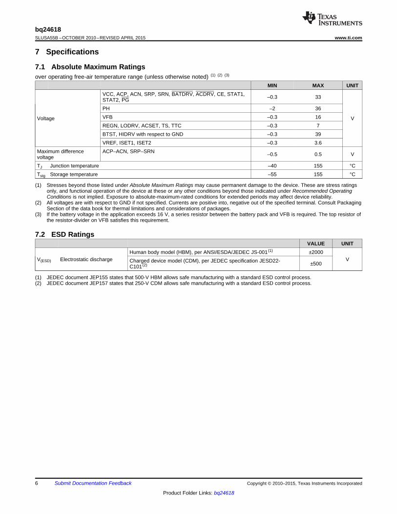
7 Specifications
7.1 Absolute Maximum Ratingsover operating free-air temperature range (unless otherwise noted) (1) (2) (3)
MIN MAX UNITVCC, ACP, ACN, SRP, SRN, BATDRV, ACDRV, CE, STAT1, –0.3 33STAT2, PGPH –2 36VFB –0.3 16Voltage VREGN, LODRV, ACSET, TS, TTC –0.3 7BTST, HIDRV with respect to GND –0.3 39VREF, ISET1, ISET2 –0.3 3.6
Maximum difference ACP–ACN, SRP–SRN –0.5 0.5 VvoltageTJ Junction temperature –40 155 °CTstg Storage temperature –55 155 °C
(1) Stresses beyond those listed under Absolute Maximum Ratings may cause permanent damage to the device. These are stress ratingsonly, and functional operation of the device at these or any other conditions beyond those indicated under Recommended OperatingConditions is not implied. Exposure to absolute-maximum-rated conditions for extended periods may affect device reliability.
(2) All voltages are with respect to GND if not specified. Currents are positive into, negative out of the specified terminal. Consult PackagingSection of the data book for thermal limitations and considerations of packages.
(3) If the battery voltage in the application exceeds 16 V, a series resistor between the battery pack and VFB is required. The top resistor ofthe resistor-divider on VFB satisfies this requirement.
7.2 ESD RatingsVALUE UNIT
Human body model (HBM), per ANSI/ESDA/JEDEC JS-001 (1) ±2000V(ESD) Electrostatic discharge VCharged device model (CDM), per JEDEC specification JESD22- ±500C101 (2)
(1) JEDEC document JEP155 states that 500-V HBM allows safe manufacturing with a standard ESD control process.(2) JEDEC document JEP157 states that 250-V CDM allows safe manufacturing with a standard ESD control process.
6 Submit Documentation Feedback Copyright © 2010–2015, Texas Instruments Incorporated
Product Folder Links: bq24618

bq24618www.ti.com SLUSA55B –OCTOBER 2010–REVISED APRIL 2015
7.3 Recommended Operating ConditionsMIN NOM MAX UNIT
VCC, ACP, ACN, SRP, SRN, BATDRV, ACDRV, CE, STAT1, STAT2, PG –0.3 28PH –2 30VFB –0.3 14
Voltage REGN, LODRV, ACSET, TS, TTC –0.3 6.5 VBTST, HIDRV with respect to GND –0.3 34ISET1, ISET2 –0.3 3.3VREF 3.3
Maximum difference ACP–ACN, SRP–SRN –0.2 0.2 VvoltageTJ Junction temperature 0 125 °C
7.4 Thermal Informationbq24616
THERMAL METRIC (1) RGE [VQFN] UNIT24 PINS
RθJA Junction-to-ambient thermal resistance 43 °C/WRθJC(top) Junction-to-case (top) thermal resistance 54.3 °C/WRθJB Junction-to-board thermal resistance 20 °C/WψJT Junction-to-top characterization parameter 0.6 °C/WψJB Junction-to-board characterization parameter 19 °C/WRθJC(bot) Junction-to-case (bottom) thermal resistance 4 °C/W
(1) For more information about traditional and new thermal metrics, see the Semiconductor and IC Package Thermal Metrics applicationreport, SPRA953.
Copyright © 2010–2015, Texas Instruments Incorporated Submit Documentation Feedback 7
Product Folder Links: bq24618

bq24618SLUSA55B –OCTOBER 2010–REVISED APRIL 2015 www.ti.com
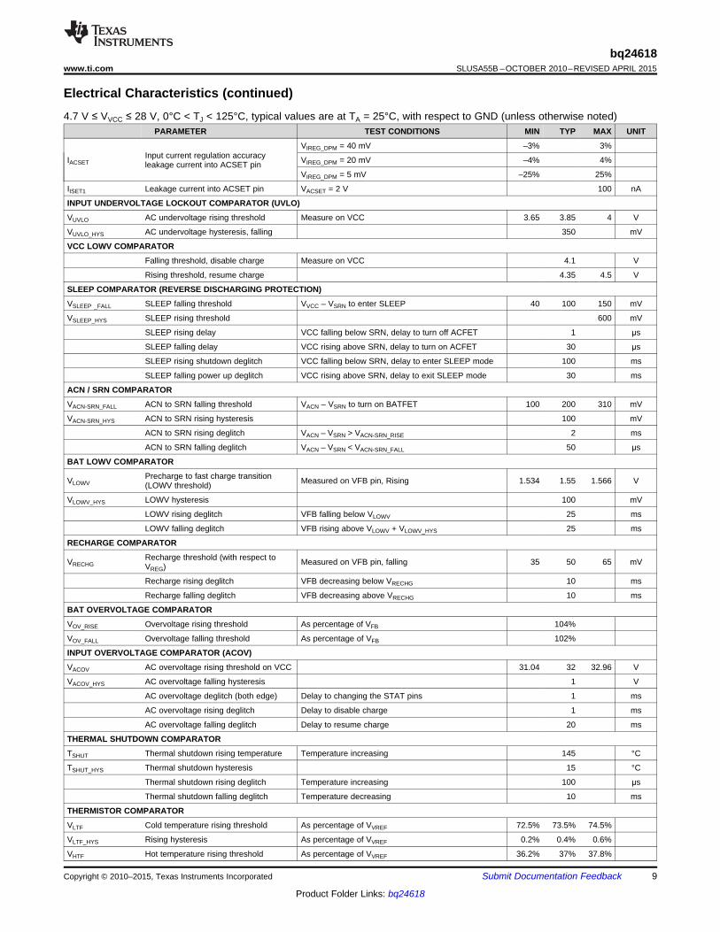
7.5 Electrical Characteristics4.7 V ≤ VVCC ≤ 28 V, 0°C < TJ < 125°C, typical values are at TA = 25°C, with respect to GND (unless otherwise noted)
PARAMETER TEST CONDITIONS MIN TYP MAX UNIT
OPERATING CONDITIONS
VVCC_OP VCC input voltage operating range 4.7 28 V
QUIESCENT CURRENTS
Total battery discharge current (sum ofcurrents into VCC, BTST, PH, ACP, VVCC < VSRN, VVCC > VUVLO (SLEEP) 15ACN, SRP, SRN, VFB), VFB ≤ 2.1 V
IBAT µAVVCC > VSRN, VVCC > VUVLO CE = LOW 5Battery discharge current (sum ofcurrents into BTST, PH, SRP, SRN, VVCC > VSRN, VVCC > VVCCLOW CE = HIGH, charge 5VFB), VFB ≤ 2.1 V done
VVCC > VSRN, VVCC > VUVLO CE = LOW (IC quiescent 1 1.5current)
Adapter supply current (current into VVCC > VSRN, VVCC > VVCCLOW , CE = HIGH, chargeIAC 2 5 mAVCC, ACP, ACN pin) done
VVCC > VSRN, VVCC > VVCCLOW , CE = HIGH, charging, 25Qg_total = 20 nC
CHARGE VOLTAGE REGULATION
VFB Feedback regulation voltage 2.1 V
TJ = 0°C to 85°C –0.5% 0.5%Charge voltage regulation accuracy
TJ = –40°C to 125°C –0.7% 0.7%
IVFB Leakage current into VFB pin VFB = 2.1 V 100 nA
CURRENT REGULATION – FAST CHARGE
VISET1 ISET1 voltage range 2 V
VIREG_CHG SRP-SRN current sense voltage range VIREG_CHG = VSRP – VSRN 100 mV
Charge current set factor (amps ofKISET1 RSENSE = 10 mΩ 5 A/Vcharge current per volt on ISET1 pin)
VIREG_CHG = 40 mV –3% 3%
VIREG_CHG = 20 mV –4% 4%Charge-current regulation accuracy
VIREG_CHG = 5 mV –25% 25%
VIREG_CHG = 1.5 mV (VSRN > 3.1 V) –40% 40%
IISET1 Leakage current into ISET1 pin VISET1 = 2 V 100 nA
CURRENT REGULATION – PRECHARGE
VISET2 ISET2 voltage range 2 V
Precharge current set factor (amps ofKISET2 Precharge current per volt on ISET2 RSENSE = 10 mΩ 1 A/V
pin)
VIREG_PRECH = 20 mV –4% 4%
Precharge-current regulation accuracy VIREG_PRECH = 5 mV –25% 25%
VIREG_PRECH = 1.5 mV (VSRN < 3.1 V) –55% 55%
IISET2 Leakage current into ISET2 pin VISET2 = 2 V 100 nA
CHARGE TERMINATION
Termination current set factor (amps ofKTERM termination current per volt on ISET2 RSENSE = 10 mΩ 1 A/V
pin)
VITERM = 20 mV –4% 4%
Termination current accuracy VITERM = 5 mV –25% 25%
VITERM = 1.5 mV –45% 45%
Deglitch time for termination (both 100 msedges)
tQUAL Termination qualification time VBAT > VRECH and ICHG < ITERM 250 ms
IQUAL Termination qualification current Discharge current once termination is detected 2 mA
INPUT CURRENT REGULATION
VACSET ACSET voltage range 2 V
VIREG_DPM ACP-ACN current sense voltage range VIREG_DPM = VACP – VACN 100 mV
Input current set factor (amps of inputKACSET RSENSE = 10 mΩ 5 A/Vcurrent per volt on ACSET pin)
8 Submit Documentation Feedback Copyright © 2010–2015, Texas Instruments Incorporated
Product Folder Links: bq24618
bq24618www.ti.com SLUSA55B –OCTOBER 2010–REVISED APRIL 2015
Electrical Characteristics (continued)4.7 V ≤ VVCC ≤ 28 V, 0°C < TJ < 125°C, typical values are at TA = 25°C, with respect to GND (unless otherwise noted)
PARAMETER TEST CONDITIONS MIN TYP MAX UNIT
VIREG_DPM = 40 mV –3% 3%Input current regulation accuracyIACSET VIREG_DPM = 20 mV –4% 4%leakage current into ACSET pin
VIREG_DPM = 5 mV –25% 25%
IISET1 Leakage current into ACSET pin VACSET = 2 V 100 nA
INPUT UNDERVOLTAGE LOCKOUT COMPARATOR (UVLO)
VUVLO AC undervoltage rising threshold Measure on VCC 3.65 3.85 4 V
VUVLO_HYS AC undervoltage hysteresis, falling 350 mV
VCC LOWV COMPARATOR
Falling threshold, disable charge Measure on VCC 4.1 V
Rising threshold, resume charge 4.35 4.5 V
SLEEP COMPARATOR (REVERSE DISCHARGING PROTECTION)
VSLEEP _FALL SLEEP falling threshold VVCC – VSRN to enter SLEEP 40 100 150 mV
VSLEEP_HYS SLEEP rising threshold 600 mV
SLEEP rising delay VCC falling below SRN, delay to turn off ACFET 1 μs
SLEEP falling delay VCC rising above SRN, delay to turn on ACFET 30 μs
SLEEP rising shutdown deglitch VCC falling below SRN, delay to enter SLEEP mode 100 ms
SLEEP falling power up deglitch VCC rising above SRN, delay to exit SLEEP mode 30 ms
ACN / SRN COMPARATOR
VACN-SRN_FALL ACN to SRN falling threshold VACN – VSRN to turn on BATFET 100 200 310 mV
VACN-SRN_HYS ACN to SRN rising hysteresis 100 mV
ACN to SRN rising deglitch VACN – VSRN > VACN-SRN_RISE 2 ms
ACN to SRN falling deglitch VACN – VSRN < VACN-SRN_FALL 50 μs
BAT LOWV COMPARATOR
Precharge to fast charge transitionVLOWV Measured on VFB pin, Rising 1.534 1.55 1.566 V(LOWV threshold)
VLOWV_HYS LOWV hysteresis 100 mV
LOWV rising deglitch VFB falling below VLOWV 25 ms
LOWV falling deglitch VFB rising above VLOWV + VLOWV_HYS 25 ms
RECHARGE COMPARATOR
Recharge threshold (with respect toVRECHG Measured on VFB pin, falling 35 50 65 mVVREG)
Recharge rising deglitch VFB decreasing below VRECHG 10 ms
Recharge falling deglitch VFB decreasing above VRECHG 10 ms
BAT OVERVOLTAGE COMPARATOR
VOV_RISE Overvoltage rising threshold As percentage of VFB 104%
VOV_FALL Overvoltage falling threshold As percentage of VFB 102%
INPUT OVERVOLTAGE COMPARATOR (ACOV)
VACOV AC overvoltage rising threshold on VCC 31.04 32 32.96 V
VACOV_HYS AC overvoltage falling hysteresis 1 V
AC overvoltage deglitch (both edge) Delay to changing the STAT pins 1 ms
AC overvoltage rising deglitch Delay to disable charge 1 ms
AC overvoltage falling deglitch Delay to resume charge 20 ms
THERMAL SHUTDOWN COMPARATOR
TSHUT Thermal shutdown rising temperature Temperature increasing 145 °C
TSHUT_HYS Thermal shutdown hysteresis 15 °C
Thermal shutdown rising deglitch Temperature increasing 100 μs
Thermal shutdown falling deglitch Temperature decreasing 10 ms
THERMISTOR COMPARATOR
VLTF Cold temperature rising threshold As percentage of VVREF 72.5% 73.5% 74.5%
VLTF_HYS Rising hysteresis As percentage of VVREF 0.2% 0.4% 0.6%
VHTF Hot temperature rising threshold As percentage of VVREF 36.2% 37% 37.8%
Copyright © 2010–2015, Texas Instruments Incorporated Submit Documentation Feedback 9
Product Folder Links: bq24618
bq24618SLUSA55B –OCTOBER 2010–REVISED APRIL 2015 www.ti.com
Electrical Characteristics (continued)4.7 V ≤ VVCC ≤ 28 V, 0°C < TJ < 125°C, typical values are at TA = 25°C, with respect to GND (unless otherwise noted)
PARAMETER TEST CONDITIONS MIN TYP MAX UNIT
VTCO Cut-off temperature rising threshold As percentage of VVREF 33.7% 34.4% 35.1%
Deglitch time for temperature out-of- VTS > VLTF, or VTS < VTCO, or VTS < VHTF 400 msrange detection
Deglitch time for temperature in-valid- VTS < VLTF – VLTF_HYS or VTS >VTCO, or VTS > VHTF 20 msrange detection
CHARGE OVERCURRENT COMPARATOR (CYCLE-BY-CYCLE)
Current rising, in nonsynchronous mode, measure on 45.5 mVV(SRP-SRN), VSRP < 2 VCharge overcurrent falling threshold
Current rising, as percentage of V(IREG_CHG), in 160%synchronous mode, VSRP > 2.2 VVOC
Minimum OCP threshold in synchronous mode,Charge overcurrent threshold floor 50measure on V(SRP-SRN), VSRP > 2.2 VmV
Maximum OCP threshold in synchronous mode,Charge overcurrent threshold ceiling 180measure on V(SRP-SRN), VSRP > 2.2 V
CHARGE UNDERCURRENT COMPARATOR (CYCLE-BY-CYCLE)
VISYNSET Charge undercurrent falling threshold Switch from SYNCH to NON-SYNCH, VSRP > 2.2 V 1 5 9 mV
BATTERY SHORTED COMPARATOR (BATSHORT)
BAT short falling threshold, forcedVBATSHT VSRP falling 2 Vnonsynchronous mode
VBATSHT_HYS BAT short rising hysteresis 200 mV
VBATSHT_DEG Deglitch on both edge 1 μs
LOW CHARGE CURRENT COMPARATOR
Low charge current (average) fallingVLC threshold to force into nonsynchronous Measure on V(SRP-SRN) 1.25 mV
mode
VLC_HYS Low charge current rising hysteresis 1.25 mV
VLC_DEG Deglitch on both edge 1 μs
VREF REGULATOR
VVREF_REG VREF regulator voltage VVCC > VUVLO, (0- to 35-mA load) 3.267 3.3 3.333 V
IVREF_LIM VREF current limit VVREF = 0 V, VVCC > VUVLO 35 mA
REGN REGULATOR
VREGN_REG REGN regulator voltage VVCC > 10 V, CE = HIGH, (0- to 40-mA load) 5.7 6.0 6.3 V
IREGN_LIM REGN current limit VREGN = 0 V, VVCC > VUVLO, CE = HIGH 40 mA
TTC INPUT AND SAFETY TIMER
TPRECHG Precharge safety timer range (1) Precharge time before fault occurs 1440 1800 2160 sec
Fast-charge safety timer range, withTCHARGE Tchg = CTTC × KTTC 1 10 Hr±10% accuracy (1)
Fast-charge timer accuracy (1) 0.01 μF ≤ CTTC ≤ 0.11 μF –10% 10%
KTTC Timer multiplier 5.6 min/nF
VTTC below this threshold disables the safety timer andTTC low threshold 0.4 Vtermination
TTC oscillator high threshold 1.5 V
TTC oscillator low threshold 1 V
TTC source/sink current 45 50 55 μA
BATTERY SWITCH (BATFET) DRIVER
RDS_BAT_OFF BATFET turnoff resistance VACN > 5 V 150 Ω
RDS_BAT_ON BATFET turnon resistance VACN > 5 V 20 kΩ
VBATDRV_REG = VACN – VBATDRV when VACN > 5 V andVBATDRV_REG BATFET drive voltage 4.2 7 VBATFET is on
VBATFET_ACN ACN voltage to keep BATFET on BATFET on 2.6 V
AC SWITCH (ACFET) DRIVER
RDS_AC_OFF ACFET turnoff resistance VVCC > 5 V 30 Ω
RDS_AC_ON ACFET turnon resistance VVCC > 5 V 20 kΩ
(1) Verified by design.
10 Submit Documentation Feedback Copyright © 2010–2015, Texas Instruments Incorporated
Product Folder Links: bq24618

bq24618www.ti.com SLUSA55B –OCTOBER 2010–REVISED APRIL 2015
Electrical Characteristics (continued)4.7 V ≤ VVCC ≤ 28 V, 0°C < TJ < 125°C, typical values are at TA = 25°C, with respect to GND (unless otherwise noted)
PARAMETER TEST CONDITIONS MIN TYP MAX UNIT
VACDRV_REG = VVCC – VACDRV when VVCC > 5 V andVACDRV_REG ACFET drive voltage 4.2 7 VACFET is on
AC / BAT MOSFET DRIVERS TIMING
Driver dead time Dead time when switching between AC and BAT 10 μs
BATTERY DETECTION
tWAKE Wake time Maximum time charge is enabled 500 ms
IWAKE Wake current RSENSE = 10 mΩ 50 125 200 mA
tDISCHARGE Discharge time Maximum time discharge current is applied 1 s
IDISCHARGE Discharge current 8 mA
IFAULT Fault current after a time-out fault 2 mA
VWAKE Wake threshold (with respect to VREG) Voltage on VFB to detect battery absent during wake 50 mV
Voltage on VFB to detect battery absent duringVDISCH Discharge threshold 1.55 Vdischarge
PWM HIGH-SIDE DRIVER (HIDRV)
High-side driver (HSD) turnonRDS_HI_ON VBTST – VPH = 5.5 V 3.3 6 Ωresistance
RDS_HI_OFF High-side driver turnoff resistance VBTST – VPH = 5.5 V 1 1.3 Ω
Bootstrap refresh comparator thresholdVBTST_REFRESH VBTST – VPH when low side refresh pulse is requested 4.0 4.2 Vvoltage
PWM LOW-SIDE DRIVER (LODRV)
RDS_LO_ON Low-side driver (LSD) turnon resistance 4.1 7 Ω
RDS_LO_OFF Low-side driver turnoff resistance 1 1.4 Ω
PWM DRIVERS TIMING
Dead time when switching between LSD and HSD, noDriver dead time 30 nsload at LSD and HSD
PWM OSCILLATOR
VRAMP_HEIGHT PWM ramp height As percentage of VCC 7%
PWM switching frequency (1) 510 600 690 kHz
INTERNAL SOFT START (8 steps to regulation current ICHG)
Soft-start steps 8 step
Soft-start step time 1.6 ms
CHARGER SECTION POWER-UP SEQUENCING
Charge enable delay after power up Delay from CE = 1 until charger is allowed to turn on 1.5 s
LOGIC IO PIN CHARACTERISTICS (CE, STAT1, STAT2, PG)
VIN_LO CE input-low threshold voltage 0.8 V
VIN_HI CE input-high threshold voltage 2.1
VBIAS_CE CE input bias current V = 3.3 V (CE has internal 1-MΩ pulldown resistor) 6 μA
STAT1, STAT2, PG output lowVOUT_LO Sink current = 5 mA 0.5 Vsaturation voltage
IOUT_HI Leakage current V = 32 V 1.2 µA
Copyright © 2010–2015, Texas Instruments Incorporated Submit Documentation Feedback 11
Product Folder Links: bq24618

t − Time = 2 s/divμ
CE
PH
LODRV
IL
5 V
/div
5 V
/div
10 V
/div
2A
/div
t − Time = 4 ms/div
CE
PH
LODRV
IBAT
5 V
/div
5 V
/div
10
V/d
iv2
A/d
iv
VCC
/PG
VREF
REGN
t − Time = 4 ms/div
5 V
/div
2 V
/div
10
V/d
iv2
V/d
iv
t − Time = 200 ms/div
PH
LODRV
IBAT
CE
5 V
/div
5 V
/div
10
V/d
iv2
A/d
iv
bq24618SLUSA55B –OCTOBER 2010–REVISED APRIL 2015 www.ti.com
7.6 Typical Characteristics
Table 1. Table of GraphsFIGURE
REF, REGN, and PG Power Up (CE = 1) Figure 1Charge Enable Figure 2Current Soft Start (CE = 1) Figure 3Charge Disable Figure 4Continuous Conduction Mode Switching Waveforms Figure 5Cycle-by-Cycle Synchronous to Nonsynchronous Figure 6100% Duty and Refresh Pulse Figure 7Transient System Load (DPM) Figure 8Battery Insertion Figure 9Battery-to-Ground Short Protection Figure 10Battery-to-Ground Short Transition Figure 11Efficiency vs Output Current Figure 12
Figure 1. REF, REGN, and PG Power Up (CE = 1) Figure 2. Charge Enable
Figure 3. Current Soft Start (CE = 1) Figure 4. Charge Disable
12 Submit Documentation Feedback Copyright © 2010–2015, Texas Instruments Incorporated
Product Folder Links: bq24618

t − Time = 200 ms/div
PH
IL
VBAT
2A
/div
5 V
/div
10
V/d
iv
t − Time = 4 ms/div
PH
IL
VBAT
LODRV
20
V/d
iv5
V/d
iv1
0 V
/div
2A
/div
t − Time = 200 s/divμ
IIN
ISYS
IBAT2A
/div
2A
/div
2A
/div
t − Time = 400 ns/div
PH
LODRV
IL
0.5
A/d
iv1
0 V
/div
5 V
/div
t − Time = 100 ns/div
HIDRV
PH
LODRV
IL
2A
/div
20
V/d
iv2
0 V
/div
5 V
/div
t − Time = 100 ns/div
PH
LODRV
IL
1A
/div
5 V
/div
5 V
/div
bq24618www.ti.com SLUSA55B –OCTOBER 2010–REVISED APRIL 2015
Figure 5. Continuous Conduction Mode Switching Figure 6. Cycle-by-Cycle Synchronous to NonsynchronousWaveform
Figure 7. 100% Duty and Refresh Pulse Figure 8. Transient System Load (DPM)
Figure 9. Battery Insertion Figure 10. Battery-to-GND Short Protection
Copyright © 2010–2015, Texas Instruments Incorporated Submit Documentation Feedback 13
Product Folder Links: bq24618

80
82
84
86
88
90
92
94
96
98
0 1 2 3 4 5 6 7 8
IBAT - Output Current - A
Eff
icie
ncy -
%
12 Vin, 1 cell
12 Vin, 2 cell20 Vin, 3 cell
20 Vin, 4 cell
t − Time = 10 s/divμ
PH
IL
VBAT
LODRV
20 V
/div
5 V
/div
10 V
/div
2A
/div
bq24618SLUSA55B –OCTOBER 2010–REVISED APRIL 2015 www.ti.com
Figure 12. Efficiency vs Output CurrentFigure 11. Battery-to-GND Short Transition
14 Submit Documentation Feedback Copyright © 2010–2015, Texas Instruments Incorporated
Product Folder Links: bq24618

VLOWV
VRECH
IPRECH
andITERM
Precharge
TimeFastcharge Safety Time
Precharge
Current
Regulation
Phase
Fastcharge Current
Regulation Phase
Fastcharge Voltage
Regulation Phase Termination
Charge
Voltage
Charge
Current
Regulation Current
Regulation Voltage
bq24618www.ti.com SLUSA55B –OCTOBER 2010–REVISED APRIL 2015
8 Detailed Description
8.1 OverviewThe bq2461x is a stand-alone, integrated Li-ion or Li-polymer battery charger that accommodates USBapplications with a minimum input voltage of 4.7 V. It employs a switched-mode synchronous buck PWMcontroller with constant switching frequency. The device controls external switches to prevent battery dischargeback to the input, to connect the adapter to the system, and to connect the battery to the system using 6-V gatedrives for better system efficiency. The bq2461x features Dynamic Power Management (DPM) which reducesbattery charge current when the input power limit is reached to avoid overloading the AC adapter when supplyingcurrent to the system and the battery charger simultaneously. A highly accurate current sense amplifier enablesprecise measurement of input current from the AC adapter to monitor the overall system power. The input currentlimit can be configured through the ACSET pin of the device.
The bq2461x has a battery detect scheme that allows it to automatically detect the presence and absence of abattery. When the battery is detected, charging begins in one of three phases (depending upon battery voltage):precharge, constant current (fast charge current regulation), and constant voltage (fast charge voltageregulation). The device will terminate charging when the termination current threshold has been reached and willbegin a recharge cycle when the battery voltage has dropped below the recharge threshold (VRECHG). Precharge,constant current, and termination current can be configured through the ISET1 and ISET2 pins, allowing forflexibility in battery charging profile. During charging, the integrated fault monitors of the device, such as batteryovervoltage protection, battery short detection (VBATSHT), thermal shutdown (internal TSHUT and TS pin), safetytimer expiration (TTC pin), and input voltage protection (VACOV), ensure battery safety.
The bq2461x has three status pins (STAT1, STAT2, and PG) to indicate the charging status and input voltage(AC adapter) status. These pins can be used to drive LEDs or communicate with a host processor.
Figure 13. Typical Charging Profile
Copyright © 2010–2015, Texas Instruments Incorporated Submit Documentation Feedback 15
Product Folder Links: bq24618

VCC
ACDRV
BATDRV
BTST
HIDRV
PH
REGN
LODRV
GND
TS
bq24618
CE
ACP
ACN
VFB
SRP
6 V LDO
V(ACP-ACN)+
-
V(SRP-SRN)
COMP
ERROR
AMPLIFIER
20µA
1V
2.1 V
IBAT_ REGSRN
VCC
VCC-6 V
LDO
STATE
MACHINE
LOGIC
BATTERY
DETECTION
LOGIC
VCC
PH
4.2V
+-
BTST REFRESH
SYSTEM
POWER
SELECTOR
LOGIC
CE
145 degC
IC Tj TSHUT
SRN+100 mV
VCC SLEEP
LEVEL
SHIFTER
ACN
+
-
+
+
-
+
-
+
-
+
-
V(SRP-SRN) CHG_OCP
+
-
160% X IBAT_REG
SYNCHSRP-SRN
ISET1
ISET2
ACSET
IBAT_ REGISET1
ISET2
5mV20X
BAT BAT_OVP
+
-
104% X VBAT_REG
LTF
+
-
HTF
VREF
TCO +
-
+
-
SUSPEND
VCC ACOV+
-
VACOV
VREF
STAT 1STAT1
20X
STAT 2STAT2
3.3 V
LDO VCC
VFB
LOWV +
-
RCHRG
+
-1.55V
+
-2.05 V
VFB
RCHRG
TERM+
-
V(SRP - SRN)
ISET2TERM
TERMINATE CHARGE
+
-
TTCTTC
+
-
+
-UVLO
VUVLO
VCC
SLEEP
UVLO
VCC-6 V
VCC-6V
ACN-6V
ACN-6 V
LDOACN ACN-6 V
ACOV
PWM
CONTROL
LOGIC
+
-
PWM
+
-
+
-
+
-
PGPG
+-
CHARGE
20 µA
DISCHARGE
CHARGE
OR
DISCHARGE
8 mA
BAT_OVP
+
-
DISABLE
TMR/TERM
0.4 V
TTC
INTERNAL
REFERENCE
VREF
ACN-SRN
SRN+200 mV
+
-
ACN
Safety
TimerTTC FAULT
2 mA
FAULT
1M
CE
-
bq24618SLUSA55B –OCTOBER 2010–REVISED APRIL 2015 www.ti.com
8.2 Functional Block Diagram
16 Submit Documentation Feedback Copyright © 2010–2015, Texas Instruments Incorporated
Product Folder Links: bq24618

ISET2PRECHARGE
SR
VI =
100 R´
ACSETDPM
AC
VI =
20 R´
ISET1CHARGE
SR
VI =
20 R´
R2V = 2.1 V 1+ ,
BAT R1
é ù´ ê ú
ë û
bq24618www.ti.com SLUSA55B –OCTOBER 2010–REVISED APRIL 2015
8.3 Feature Description
8.3.1 Battery Voltage RegulationThe bq24618 uses a high-accuracy voltage band gap and regulator for the high charging voltage accuracy. Thecharge voltage is programmed through a resistor divider from the battery to ground, with the midpoint tied to theVFB pin. The voltage at the VFB pin is regulated to 2.1 V, giving the following equation for the regulation voltage:
where• R2 is connected from VFB to the battery.• R1 is connected from VFB to GND. (1)
8.3.2 Battery Current RegulationThe ISET1 input sets the maximum fast-charging current. Battery charge current is sensed by resistor RSRconnected between SRP and SRN. The full-scale differential voltage between SRP and SRN is 100 mV. Thus,for a 10-mΩ sense resistor, the maximum charging current is 10 A. The equation for charge current is:
(2)
VISET1, the input voltage range of ISET1, is from 0 V to 2 V. The SRP and SRN pins are used to sense voltageacross RSR using the default value of 10 mΩ. However, resistors of other values can also be used. A largersense resistor gives a larger sense voltage and a higher regulation accuracy, but at the expense of higherconduction loss.
8.3.3 Input Adapter Current RegulationThe total input from an AC adapter or other DC source is a function of the system supply current and the batterycharging current. System current normally fluctuates as portions of the systems are powered up or down. WithoutDPM, the source must be able to supply the maximum system current and the maximum charger input currentsimultaneously. By using DPM, the battery charger reduces the charging current when the input current exceedsthe input current limit set by ACSET. The current capability of the AC adaptor can be lowered, reducing systemcost.
Similar to sensing battery regulation current, adaptor current is sensed by resistor RAC connected between ACPand ACN. Its maximum value is set by ACSET using Equation 3:
(3)
VACSET, the input voltage range of ACSET, is from 0 V to 2 V. The ACP and ACN pins are used to sense voltageacross RAC using the default value of 10 mΩ. However, resistors of other values can also be used. A largersense resistor gives a larger sense voltage and a higher regulation accuracy, but at the expense of higherconduction loss.
8.3.4 PrechargeOn power up, if the battery voltage is below the VLOWV threshold, the bq24618 applies the precharge current tothe battery. This feature is intended to revive deeply discharged cells. If the VLOWV threshold is not reached within30 minutes of initiating precharge, the charger turns off and a FAULT is indicated on the status pins.
The precharge current is determined by the voltage on the ISET2 pin, VISET2, according to Equation 4.
(4)
Copyright © 2010–2015, Texas Instruments Incorporated Submit Documentation Feedback 17
Product Folder Links: bq24618

CHARGE TTC TTCt = C K´
ISET2TERM
SR
VI =
100 R´
bq24618SLUSA55B –OCTOBER 2010–REVISED APRIL 2015 www.ti.com
Feature Description (continued)8.3.5 Charge Termination, Recharge, and Safety TimerThe bq24618 monitors the charging current during the voltage regulation phase. When VTTC is valid, terminationis detected while the voltage on the VFB pin is higher than the VRECH threshold AND the charge current is lessthan the ITERM threshold, as calculated in Equation 5:
(5)
The input voltage of ISET2 is from 0 V to 2 V. The minimum precharge and termination current is clamped to bearound 125 mA with default 10-mΩ sensing resistor. As a safety backup, the bq24618 also provides aprogrammable charge timer. The charge time is programmed by the capacitor connected between the TTC pinand GND, and is given by Equation 6
where• CTTC (range from 0.01 µF to 0.11 µF to give 1-h to 10-h safety time) is the capacitor connected from the TTC
pin to GND.• KTTC is the constant multiplier (5.6 min/nF). (6)
A new charge cycle is initiated and the safety timer is reset when any of the following conditions occurs:• The battery voltage falls below the recharge threshold.• A power-on-reset (POR) event occurs.• CE is toggled.
The TTC pin may be taken LOW to disable termination and to disable the safety timer. If TTC is pulled to VREF,the bq24618 continues to allow termination but disable the safety timer. TTC taken low resets the safety timer.When ACOV, VCCLOWV, and SLEEP mode resume normal, the safety timer is reset.
8.3.6 Power UpThe bq24618 uses a SLEEP comparator to determine the source of power on the VCC pin, because VCC can besupplied either from the battery or the adapter. If the VCC voltage is greater than the SRN voltage, the bq24618enables the ACFET and disables BATFET. If all other conditions are met for charging, the bq24618 thenattempts to charge the battery (see Enable and Disable Charging). If the SRN voltage is greater than VCC,indicating that the battery is the power source, the bq24618 enables the BATFET and enters a low quiescentcurrent (<15-μA) SLEEP mode to minimize current drain from the battery.
If VCC is below the UVLO threshold, the device is disabled, ACFET turns off, and BATFET turns on.
8.3.7 Enable and Disable ChargingThe following conditions must be valid before charge is enabled:• CE is HIGH.• The device is not in UVLO and not in VCCLOWV mode.• The device is not in SLEEP mode.• The VCC voltage is lower than the AC overvoltage threshold (VCC < VACOV).• 30-ms delay is complete after initial power up.• The REGN LDO and VREF LDO voltages are at the correct levels.• Thermal shutdown (TSHUT) is not valid.• TS fault is not detected.
Any of the following conditions will stop ongoing charging:• CE is LOW.• Adapter is removed, causing the device to enter UVLO, VCCLOWV, or SLEEP mode.• Adapter is over voltage.• The REGN or VREF LDOs are overloaded.• TSHUT IC temperature threshold is reached (145°C on rising edge with 15°C hysteresis).
18 Submit Documentation Feedback Copyright © 2010–2015, Texas Instruments Incorporated
Product Folder Links: bq24618

o
o o
1=
2 L C
fp
bq24618www.ti.com SLUSA55B –OCTOBER 2010–REVISED APRIL 2015
Feature Description (continued)• TS voltage goes out of range, indicating the battery temperature is too hot or too cold.• TTC safety timer times out.
8.3.8 System Power SelectorThe bq24618 automatically switches adapter or battery power to the system load. The battery is connected to thesystem by default during power up or during SLEEP mode. The battery is disconnected from the system, andthen the adapter is connected to the system 30 ms after exiting SLEEP. An automatic break-before-make logicprevents shoot-through currents when the selectors switch.
The ACDRV is used to drive a pair of back-to-back P-channel power MOSFETs between the adapter and ACPwith sources connected together and to VCC. The FET connected to the adapter prevents reverse dischargefrom the battery to the adapter when turned off. The P-channel FET with the drain connected to the adapter inputprovides reverse battery discharge protection when off; and also minimizes system power dissipation with its lowrDS(on), compared to a Schottky diode. The other P-channel FET connected to ACP separates the battery fromthe adapter and provides a limited dI/dt when connecting the adapter to the system by controlling the FET turnontime. The BATDRV controls a P-channel power MOSFET placed between BAT and the system.
When an adapter is not detected, the ACDRV is pulled to VCC to keep ACFET off, disconnecting the adapterfrom system. BATDRV stays at ACN-6V to connect the battery to the system.
Approximately 30 ms after the device comes out of SLEEP mode, the system begins to switch from battery toadapter. The break-before-make logic keeps both ACFET and BATFET off for 10 µs before ACFET turns on.This prevents shoot-through current or any large discharging current from going into the battery. BATDRV ispulled up to ACN and the ACDRV pin is set to VCC-6V by an internal regulator to turn on P-channel ACFET,connecting the adapter to the system.
When the adapter is removed, the system waits until VCC drops back to within 200 mV above SRN to switchfrom the adapter back to the battery. The break-before-make logic still keeps 10-μs dead time. The ACDRV ispulled up to VCC and the BATDRV pin is set to ACN-6V by an internal regulator to turn on P-channel BATFET,connecting the battery to the system.
Asymmetrical gate drive (fast turnoff and slow turnon) for the ACDRV and BATDRV drivers provides fast turn-offand slow turn-on of the ACFET and BATFET to help the break-before-make logic and to allow a soft-start atturnon of either FET. The soft-start time can be further increased by putting a capacitor from the gate to thesource of the P-channel power MOSFETs.
8.3.9 Automatic Internal Soft-Start Charger CurrentThe charger automatically soft-starts the charger regulation current every time the charger goes into fast chargeto ensure there is no overshoot or stress on the output capacitors or the power converter. The soft-start consistsof stepping up the charge regulation current in eight evenly divided steps up to the programmed charge current.Each step lasts around 1.6 ms, for a typical rise time of 12.8 ms. No external components are needed for thisfunction.
8.3.10 Converter OperationThe synchronous buck PWM converter uses a fixed-frequency voltage mode with a feed-forward control scheme.A type-III compensation network allows using ceramic capacitors at the output of the converter. Thecompensation input stage is connected internally between the feedback output (FBO) and the error amplifierinput (EAI). The feedback compensation stage is connected between the error amplifier input (EAI) and erroramplifier output (EAO). The LC output filter is selected to give a resonant frequency of 12 kHz–17 kHz for thebq24618, where the resonant frequency, fo, is given by:
(7)
An internal sawtooth ramp is compared to the internal EAO error control signal to vary the duty cycle of theconverter. The ramp height is 7% of the input adapter voltage, making it always directly proportional to the inputadapter voltage. This cancels out any loop gain variation due to a change in input voltage and simplifies the loopcompensation. The ramp is offset by 300 mV in order to allow zero-percent duty cycle when the EAO signal isbelow the ramp. The EAO signal is also allowed to exceed the sawtooth ramp signal in order to get a 100% duty-
Copyright © 2010–2015, Texas Instruments Incorporated Submit Documentation Feedback 19
Product Folder Links: bq24618

bq24618SLUSA55B –OCTOBER 2010–REVISED APRIL 2015 www.ti.com
Feature Description (continued)cycle PWM request. Internal gate-drive logic allows achieving 99.5% duty cycle while ensuring the N-channelupper device always has enough voltage to stay fully on. If the BTST pin to PH pin voltage falls below 4.2 V formore than three cycles, then the high-side N-channel power MOSFET is turned off and the low-side N-channelpower MOSFET is turned on to pull the PH node down and recharge the BTST capacitor. Then the high-sidedriver returns to 100% duty-cycle operation until the BTST-to-PH voltage is detected to fall low again due toleakage current discharging the BTST capacitor below 4.2 V, and the reset pulse is reissued.
The fixed-frequency oscillator keeps tight control of the switching frequency under all conditions of input voltage,battery voltage, charge current, and temperature, simplifying output filter design and keeping it out of the audiblenoise region. Also see Application and Implementation for selection of the inductor, capacitor, and MOSFET.
8.3.11 Synchronous and Nonsynchronous OperationThe charger operates in synchronous mode when the SRP-SRN voltage is above 5 mV (0.5-A inductor currentfor a 10-mΩ sense resistor). During synchronous mode, the internal gate-drive logic ensures there is break-before-make complementary switching to prevent shoot-through currents. During the 30-ns dead time where bothFETs are off, the body diode of the low-side power MOSFET conducts the inductor current. Having the low-sideFET turn on keeps the power dissipation low and allows safely charging at high currents. During synchronousmode, the inductor current is always flowing and the converter operates in Continuous Conduction Mode (CCM),creating a fixed two-pole system.
The charger operates in nonsynchronous mode when the SRP-SRN voltage is below 5 mV (0.5-A inductorcurrent for a 10-mΩ sense resistor). The charger is forced into nonsynchronous mode when battery voltage islower than 2 V or when the average SRP-SRN voltage is lower than 1.25 mV.
During nonsynchronous operation, the body diode of the low-side MOSFET can conduct the positive inductorcurrent after the high-side N-channel power MOSFET turns off. When the load current decreases and theinductor current drops to zero, the body diode is naturally turned off and the inductor current becomesdiscontinuous. This mode is called Discontinuous Conduction Mode (DCM). During DCM, the low-side N-channelpower MOSFET turns on for around 80 ns when the bootstrap capacitor voltage drops below 4.2 V. Then thelow-side power MOSFET turns off and stays off until the beginning of the next cycle, where the high-side powerMOSFET is turned on again. The 80-ns low-side MOSFET on-time is required to ensure the bootstrap capacitoris always recharged and able to keep the high-side power MOSFET on during the next cycle. This is importantfor battery chargers, where unlike regular DC-DC converters, there is a battery load that maintains a voltage andcan both source and sink current. The 80-ns low-side pulse pulls the PH node (the connection between high- andlow-side MOSFETs) down, allowing the bootstrap capacitor to recharge up to the REGN LDO value. After 80 ns,the low-side MOSFET is kept off to prevent negative inductor current from occurring.
At very low currents during nonsynchronous operation, there may be a small amount of negative inductor currentduring the 80-ns recharge pulse. The charge should be low enough to be absorbed by the input capacitance.Whenever the converter goes into zero-percent duty cycle, the high-side MOSFET does not turn on, and the low-side MOSFET does not turn on (only 80-ns recharge pulse) either, and there is almost no discharge from thebattery.
During the DCM mode, the loop response automatically changes and has a single pole system at which the poleis proportional to the load current, because the converter does not sink current, and only the load provides acurrent sink. This means at very low currents the loop response is slower, as there is less sinking currentavailable to discharge the output voltage.
8.3.12 Cycle-by-Cycle Charge Undercurrent ProtectionIf the SRP-SRN voltage decreases below 5 mV (the charger is also forced into nonsynchronous mode when theaverage SRP-SRN voltage is lower than 1.25 mV), the low-side FET is turned off for the remainder of theswitching cycle to prevent negative inductor current. During DCM, the low-side FET only turns on for around 80ns when the bootstrap capacitor voltage drops below 4.2 V to provide refresh charge for the bootstrap capacitor.This is important to prevent negative inductor current from causing a boost effect in which the input voltageincreases as power is transferred from the battery to the input capacitors and leads to an overvoltage stress onthe VCC node, potentially causing damage to the system.
20 Submit Documentation Feedback Copyright © 2010–2015, Texas Instruments Incorporated
Product Folder Links: bq24618
bq24618www.ti.com SLUSA55B –OCTOBER 2010–REVISED APRIL 2015
Feature Description (continued)8.3.13 Input Overvoltage Protection (ACOV)ACOV provides protection to prevent system damage due to high input voltage. Once the adapter voltagereaches the ACOV threshold, charge is disabled and the system is switched to the battery instead of the adapter.
8.3.14 Input Undervoltage Lockout (UVLO)The system must have a minimum VCC voltage to allow proper operation. This VCC voltage could come fromeither the input adapter or the battery, because a conduction path exists from the battery to VCC through thehigh-side NMOS body diode. When VCC is below the UVLO threshold, all circuits on the IC are disabled, and thegate-drive bias to ACFET and BATFET is disabled.
8.3.15 Battery Overvoltage ProtectionThe converter does not allow the high-side FET to turn on until the BAT voltage goes below 102% of theregulation voltage. This allows one-cycle response to an overvoltage condition, such as occurs when the load isremoved or the battery is disconnected. An 8-mA current sink from SRP to GND is on only during charge andallows discharging the stored output inductor energy that is transferred to the output capacitors. BATOVP alsosuspends the safety timer.
8.3.16 Cycle-by-Cycle Charge Overcurrent ProtectionThe charger has secondary cycle-to-cycle overcurrent protection. It monitors the charge current, and preventsthe current from exceeding 160% of the programmed charge current. The high-side gate drive turns off when theovercurrent is detected, and automatically resumes when the current falls below the overcurrent threshold.
8.3.17 Thermal Shutdown ProtectionThe QFN package has low thermal impedance, which provides good thermal conduction from the silicon to theambient, to keep junction temperature low. As an added level of protection, the charger converter turns off andself-protects whenever the junction temperature exceeds the TSHUT threshold of 145°C. The charger stays offuntil the junction temperature falls below 130°C; then the charger soft-starts again if all other charge enablingconditions are valid. Thermal shutdown also suspends the safety timer.
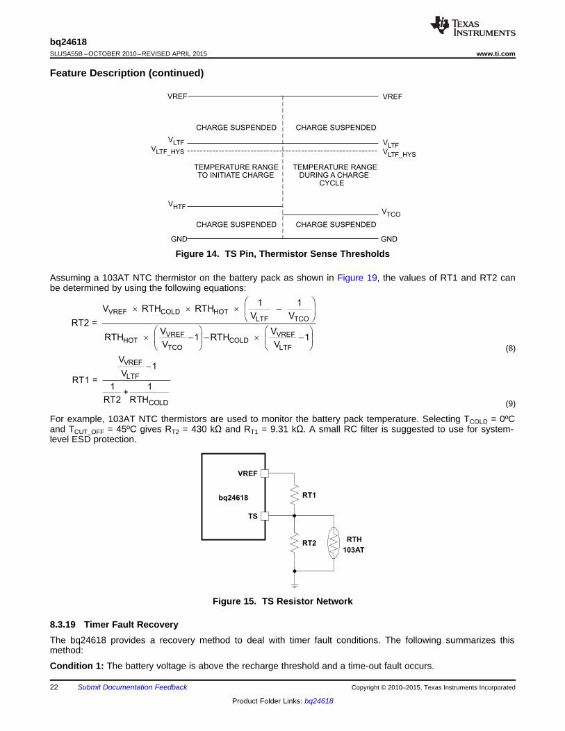
8.3.18 Temperature QualificationThe controller continuously monitors battery temperature by measuring the voltage between the TS pin andGND. A negative temperature coefficient thermistor (NTC) and an external voltage divider typically develop thisvoltage. The controller compares this voltage against its internal thresholds to determine if charging is allowed.To initiate a charge cycle, the battery temperature must be within the VLTF and VHTF thresholds. If batterytemperature is outside of this range, the controller suspends charge and the safety timer and waits until thebattery temperature is within the VLTF to VHTF range. During the charge cycle, the battery temperature must bewithin the VLTF and VTCO thresholds. If battery temperature is outside of this range, the controller suspendscharge and waits until the battery temperature is within the VLTF to VHTF range. The controller suspends chargeby turning off the PWM charge FETs. Figure 14 summarizes the operation.
Copyright © 2010–2015, Texas Instruments Incorporated Submit Documentation Feedback 21
Product Folder Links: bq24618
VREF
TS
RT2
RT1
RTH
103AT
bq24618
VREF
LTF
COLD
V1
VRT1 =
1 1+
RT2 RTH
-
æ ö´ ´ ´ -ç ÷
è ø
æ ö æ ö´ - - ´ -ç ÷ ç ÷
è øè ø
VREF COLD HOT
LTF TCO
VREF VREFHOT COLD
TCO LTF
1 1V RTH RTH
V VRT2 =
V VRTH 1 RTH 1
V V
CHARGE SUSPENDED CHARGE SUSPENDED
TEMPERATURE RANGETO INITIATE CHARGE
TEMPERATURE RANGEDURING A CHARGE
CYCLE
VLTF
GND
VTCO
GND
VLTF_HYS
VREF VREF
CHARGE SUSPENDED CHARGE SUSPENDED
VHTF
VLTFVLTF_HYS
bq24618SLUSA55B –OCTOBER 2010–REVISED APRIL 2015 www.ti.com
Feature Description (continued)
Figure 14. TS Pin, Thermistor Sense Thresholds
Assuming a 103AT NTC thermistor on the battery pack as shown in Figure 19, the values of RT1 and RT2 canbe determined by using the following equations:
(8)
(9)
For example, 103AT NTC thermistors are used to monitor the battery pack temperature. Selecting TCOLD = 0ºCand TCUT_OFF = 45ºC gives RT2 = 430 kΩ and RT1 = 9.31 kΩ. A small RC filter is suggested to use for system-level ESD protection.
Figure 15. TS Resistor Network
8.3.19 Timer Fault RecoveryThe bq24618 provides a recovery method to deal with timer fault conditions. The following summarizes thismethod:
Condition 1: The battery voltage is above the recharge threshold and a time-out fault occurs.
22 Submit Documentation Feedback Copyright © 2010–2015, Texas Instruments Incorporated
Product Folder Links: bq24618

bq24618www.ti.com SLUSA55B –OCTOBER 2010–REVISED APRIL 2015
Feature Description (continued)Recovery Method: The timer fault clears when the battery voltage falls below the recharge threshold, andbattery detection begins. A POR condition or taking CE low also clears the fault.
Condition 2: The battery voltage is below the recharge threshold and a time-out fault occurs.
Recovery Method: Under this scenario, the bq24618 applies the IFAULT current to the battery. This small currentis used to detect a battery-removal condition and remains on as long as the battery voltage stays below therecharge threshold. If the battery voltage goes above the recharge threshold, the bq24618 disables the faultcurrent and executes the recovery method described in Condition 1. A POR condition or taking CE low alsoclears the fault.
8.3.20 PG OutputThe open-drain PG (power-good) output indicates whether the VCC voltage is valid or not. The open-drain FETturns on whenever the bq24618 has a valid VCC input (not in UVLO or ACOV or SLEEP mode). The PG pin canbe used to drive an LED or communicate to the host processor.
8.3.21 CE (Charge Enable)The CE digital input is used to disable or enable the charge process. A high-level signal on this pin enablescharge, provided all the other conditions for charge are met (see Enable and Disable Charging). A high-to-lowtransition on this pin also resets all timers and fault conditions. There is an internal 1-MΩ pulldown resistor on theCE pin, so if CE is floated, the charge does not turn on.
8.3.22 Charge Status OutputsThe open-drain STAT1 and STAT2 outputs indicate various charger operations as shown in Table 2. Thesestatus pins can be used to drive LEDs or communicate with the host processor. OFF indicates that the open-drain transistor is turned off.
Table 2. STAT Pin Definition for bq24618CHARGE STATE STAT1 STAT2
Charge in progress ON OFFCharge complete OFF ONCharge suspend, timer fault, overvoltage, sleep mode, battery absent OFF OFF
Copyright © 2010–2015, Texas Instruments Incorporated Submit Documentation Feedback 23
Product Folder Links: bq24618

POR or RECHARGE
Enable 125-mA Charge,
Start 0.5-s timer
VFB > VRECH No
Battery Present,
Begin Charge
0.5-s timer
expired
Yes
No
Yes
Disable 125-mA
Charge
Apply 8-mA discharge
current, start 1-s timer
VFB < VLOWV No
Battery Present,
Begin Charge
1-s timer
expired
Yes
No
Yes
Disable 8-mA
discharge current
The battery detection routine runs on
power up, or if VFB falls below VRECH
due to removing a battery or
discharging a battery
Battery Absent
bq24618SLUSA55B –OCTOBER 2010–REVISED APRIL 2015 www.ti.com
8.3.23 Battery DetectionFor applications with removable battery packs, the bq24618 provides a battery-absent detection scheme toreliably detect insertion or removal of battery packs.
Figure 16. Battery-Detection Flow Chart
Once the device has powered up, an 8-mA discharge current is applied to the SRN terminal. If the batteryvoltage falls below the LOWV threshold within 1 second, the discharge source is turned off, and the charger isturned on at low charge current (125 mA). If the battery voltage rises above the recharge threshold within 500ms, there is no battery present and the cycle restarts. If either the 500-ms or 1-second timer times out before itsrespective threshold is hit, a battery is detected and a charge cycle is initiated.
24 Submit Documentation Feedback Copyright © 2010–2015, Texas Instruments Incorporated
Product Folder Links: bq24618
MAX
8mA 1secC = = 2.7 mF
500k0.5 1+
100k
´
é ù´ ê ú
ë û
DISCH DISCHMAX
2
1
I tC =
R0.5 1+
R
´
é ù´ ê ú
ë û
VRECH
VLOWV
Battery
inserted
Battery not detected
tWAKE
Battery detected
tLOWV_DEG
tRECH_DEG
VREG
( )VWAKE
( )VDISH
bq24618www.ti.com SLUSA55B –OCTOBER 2010–REVISED APRIL 2015
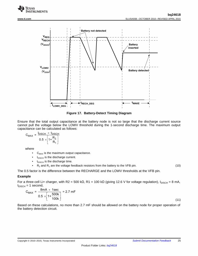
Figure 17. Battery-Detect Timing Diagram
Ensure that the total output capacitance at the battery node is not so large that the discharge current sourcecannot pull the voltage below the LOWV threshold during the 1-second discharge time. The maximum outputcapacitance can be calculated as follows:
where• CMAX is the maximum output capacitance.• IDISCH is the discharge current.• tDISCH is the discharge time.• R2 and R1 are the voltage feedback resistors from the battery to the VFB pin. (10)
The 0.5 factor is the difference between the RECHARGE and the LOWV thresholds at the VFB pin.
ExampleFor a three-cell Li+ charger, with R2 = 500 kΩ, R1 = 100 kΩ (giving 12.6 V for voltage regulation), IDISCH = 8 mA,tDISCH = 1 second,
(11)
Based on these calculations, no more than 2.7 mF should be allowed on the battery node for proper operation ofthe battery detection circuit.
Copyright © 2010–2015, Texas Instruments Incorporated Submit Documentation Feedback 25
Product Folder Links: bq24618
bq24618SLUSA55B –OCTOBER 2010–REVISED APRIL 2015 www.ti.com
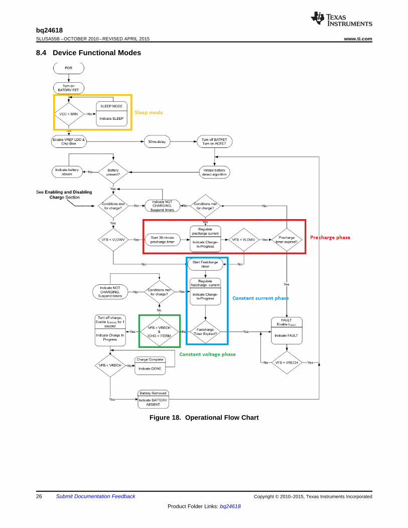
8.4 Device Functional Modes
Figure 18. Operational Flow Chart
26 Submit Documentation Feedback Copyright © 2010–2015, Texas Instruments Incorporated
Product Folder Links: bq24618

RAC0.010 W
Q1 (ACFET)
N
P
ACN
ACP
ISET2
ACSET
VREF
CE
VFB
TS
VCC
HIDRV
N
PH
BTST
REGN
LODRV
GND
SRP
SRN
P
PACK+
PACK-
SYSTEMADAPTER+
ADAPTER-
C4
0.1 µF
C2 0.1 µFC3 C7
Q4
Q5
C6
L1
6.8 µH*D1
BAT54
C5
C10
0.1 µF
TTC
CTTC
VREF
STAT2
PackThermistor
Sense
BATDRVACDRV
bq24618
P
Q2 (ACFET)
Q3 (BATFET)VREF
ISET1
STAT1
VBAT
R99.31 kW
R10
430 kW
R1100kW
PG
ADAPTER +
Cff22 pF
0.1 µF
1µF
C810 µF
1 µF
1 µF
RSR0.010 W
C11
0.1 µF
C12
10 µF*
C13
10 µF*
R2500 kΩ
R12 10 kW
R11 10 kW
R13 10 kW
R3100 kW
R432.4 kW
R5100 kW
R610 kW
R7100 kW
R822.1 kW
R14100 kW
C140.1 mF
R15100 kW
C15
0.1 µF
PwrPad0.056 Fμ
R16
100 W
C10.1 Fμ103AT
SI7617DN
SI7616DN
SIS412DN
SIS412DN
SI7617DN
C910 μF
R1710Ω
R202Ω
C162.2μF
R181 kΩ
R191 kΩ
D2
D3
D4
bq24618www.ti.com SLUSA55B –OCTOBER 2010–REVISED APRIL 2015
9 Application and Implementation
NOTEInformation in the following applications sections is not part of the TI componentspecification, and TI does not warrant its accuracy or completeness. TI’s customers areresponsible for determining suitability of components for their purposes. Customers shouldvalidate and test their design implementation to confirm system functionality.
9.1 Application InformationThe bq24618 battery charger is ideal for high current charging (up to 10 A) and can charge battery packsconsisting of single cells or multiple cells in series. The bq24610EVM evaluation module is a complete chargemodule for evaluating the bq2461x. The application curves were taken using the bq24610EVM. Refer to the EVMuser's guide (SLUU396) for EVM information.
9.2 Typical Application
VIN = 19 V, 3-cell, Iadapter_limit = 4 A, Icharge = 3 A, Ipre-charge = Iterm = 0.3 A, 5-hour safety timer
Figure 19. Typical System Schematic
Copyright © 2010–2015, Texas Instruments Incorporated Submit Documentation Feedback 27
Product Folder Links: bq24618

CIN CHGI = I D (1 D)´ ´ -
INRIPPLE
S
V D (1 D)I =
f L
´ ´ -
´
SAT CHG RIPPLEI I + (1/2) I³
bq24618SLUSA55B –OCTOBER 2010–REVISED APRIL 2015 www.ti.com
Typical Application (continued)9.2.1 Design RequirementsFor this design example, use the parameters listed in Table 3 as the input parameters.
Table 3. Design ParametersDESIGN PARAMETER VALUE
AC adapter voltage (VIN) 19 VAC adapter current limit 4 ABattery charge voltage (number of cells in series) 12.6 V (3 cells)Battery charge current (during constant current phase) 3 APrecharge and termination current 0.3 ASafety timer 5 hours
9.2.2 Detailed Design Procedure
9.2.2.1 Inductor SelectionThe bq2461x has 600-kHz switching frequency to allow the use of small inductor and capacitor values. Inductorsaturation current should be higher than the charging current (ICHG) plus half the ripple current (IRIPPLE):
(12)
The inductor ripple current depends on input voltage (VIN), duty cycle (D = VOUT/VIN), switching frequency (fS) andinductance (L):
(13)
The maximum inductor ripple current happens with D = 0.5 or close to 0.5. For example, the battery chargingvoltage range is from 9 V to 12.6 V for a three-cell battery pack. For 20-V adapter voltage, 10-V battery voltagegives the maximum inductor ripple current. Another example is a four-cell battery, where the battery voltagerange is from 12 V to 16.8 V, and 12-V battery voltage gives the maximum inductor ripple current.
Usually inductor ripple is designed in the range of 20% to 40% of maximum charging current as a trade-offbetween inductor size and efficiency for a practical design.
The bq24618 has cycle-by-cycle charge undercurrent protection (UCP) by monitoring the charge current-sensingresistor to prevent negative inductor current. The typical UCP threshold is 5 mV falling edge, corresponding to0.5 A falling edge for a 10-mΩ charge current-sensing resistor.
9.2.2.2 Input CapacitorThe input capacitor should have enough ripple current rating to absorb the input switching ripple current. Theworst-case RMS ripple current is half of the charging current when the duty cycle is 0.5. If the converter does notoperate at 50% duty cycle, then the worst-case capacitor RMS current ICIN occurs where the duty cycle is closestto 50% and can be estimated by the following equation:
(14)
A low-ESR ceramic capacitor such as X7R or X5R is preferred for the input decoupling capacitor and should beplaced as close as possible to the drain of the high-side MOSFET and source of the low-side MOSFET. Thevoltage rating of the capacitor must be higher than the normal input voltage level. A 25-V rating or highercapacitor is preferred for 20-V input voltage. A 10-µF to 20-µF capacitor is suggested for typical 3-A to 4-Acharging current.
9.2.2.3 Output CapacitorThe output capacitor also should have enough ripple current rating to absorb output switching ripple current. Theoutput capacitor RMS current ICOUT is given:
28 Submit Documentation Feedback Copyright © 2010–2015, Texas Instruments Incorporated
Product Folder Links: bq24618

REGN plt plton off
on off
V V VI = , I =
R R
-
SW GD GS
1Q = Q + Q
2´
SW SWon off
on off
Q Qt = , t =
I I
( )2top CHG DS(on) IN CHG on off S
1P = D I R + V I t + t f
2´ ´ ´ ´ ´ ´
top DS(on) GD bottom DS(on) GFOM = R Q FOM = R Q´ ´
æ öD = -ç ÷
ç ÷è ø
2
BATo BAT2
INs
V1V V
V8LCf
RIPPLECOUT RIPPLE
II = 0.29 I
2 3
» ´
´
bq24618www.ti.com SLUSA55B –OCTOBER 2010–REVISED APRIL 2015
(15)
The output capacitor voltage ripple can be calculated as follows:
(16)
At certain input/output voltage and switching frequency, the voltage ripple can be reduced by increasing theoutput filter LC.
The bq24618 has an internal loop compensator. To get good loop stability, the resonant frequency of the outputinductor and output capacitor should be designed from 12 kHz to 17 kHz. The preferred ceramic capacitor is 25-V or higher rating, X7R or X5R for 4-cell applications.
9.2.2.4 Power MOSFET SelectionTwo external N-channel MOSFETs are used for a synchronous switching battery charger. The gate drivers areinternally integrated into the IC with 6 V of gate drive voltage. MOSFETs of 30-V or higher voltage rating arepreferred for 20-V input voltage and 40-V or higher rating MOSFETs are preferred for 20-V to 28-V input voltage.
Figure-of-merit (FOM) is usually used for selecting proper the MOSFET, based on a trade-off between theconduction loss and switching loss. For a top-side MOSFET, FOM is defined as the product of a MOSFET ON-resistance, rDS(on), and the gate-to-drain charge, QGD. For a bottom-side MOSFET, FOM is defined as the productof the MOSFET ON-resistance, rDS(on), and the total gate charge, QG.
(17)
The lower the FOM value, the lower the total power loss. Usually, lower rDS(on) has higher cost with the samepackage size.
The top-side MOSFET loss includes conduction loss and switching loss. It is a function of duty cycle (D =VOUT/VIN), charging current (ICHG), MOSFET ON-resistance rDS(on)), input voltage (VIN), switching frequency (fS),turnon time (ton) and turnoff time (toff):
(18)
The first item represents the conduction loss. Usually MOSFET rDS(on) increases by 50% with a 100ºC junctiontemperature rise. The second term represents the switching loss. The MOSFET turnon and turnoff times aregiven by:
where• Qsw is the switching charge.• Ion is the turnon gate-drive current.• Ioff is the turnoff gate-drive current. (19)
If the switching charge is not given in the MOSFET data sheet, it can be estimated by gate-to-drain charge (QGD)and gate-to-source charge (QGS):
(20)
Total gate drive current can be estimated by the REGN voltage (VREGN), MOSFET plateau voltage (Vplt), totalturnon gate resistance (Ron), and turnoff gate resistance (Roff) of the gate driver:
(21)
The conduction loss of the bottom-side MOSFET is calculated with the following equation when it operates insynchronous continuous conduction mode:
Copyright © 2010–2015, Texas Instruments Incorporated Submit Documentation Feedback 29
Product Folder Links: bq24618

R12 W
C12.2 mF
D1
C20.1-1 mF
R24.7-30WAdapter
connectorVCC pin
(2010)(1206)
ICLoss_driver IN g_total sP V Q f= × ×
2bottom CHG DS(on)P = (1 D) I R- ´ ´
bq24618SLUSA55B –OCTOBER 2010–REVISED APRIL 2015 www.ti.com
(22)
If the SRP-SRN voltage decreases below 5 mV (the charger is also forced into nonsynchronous mode when theaverage SRP-SRN voltage is lower than 1.25 mV), the low-side FET is turned off for the remainder of theswitching cycle to prevent negative inductor current.
As a result, all the freewheeling current goes through the body diode of the bottom-side MOSFET. The maximumcharging current in nonsynchronous mode can be up to 0.9 A (0.5 A typical) for a 10-mΩ charging currentsensing resistor, considering IC tolerance. Choose the bottom-side MOSFET with either an internal Schottky orbody diode capable of carrying the maximum nonsynchronous mode charging current.
MOSFET gate driver power loss contributes to the dominant losses on the controller IC when the buck converteris switching. Choosing a MOSFET with a small Qg_total reduces the IC power loss to avoid thermal shutdown.
where• Qg_total is the total gate charge for both upper and lower MOSFET at 6 V VREGN. (23)
9.2.2.5 Input Filter DesignDuring adapter hot plug-in, the parasitic inductance and input capacitor from the adapter cable form a second-order system. The voltage spike at the VCC pin may be beyond the IC maximum voltage rating and damage theIC. The input filter must be carefully designed and tested to prevent an overvoltage event on the VCC pin. TheACP/ACN pin must be placed after the input ACFET in order to avoid overvoltage stress on these pins during hotplug-in.
There are several methods to damping or limiting the overvoltage spike during adapter hot plug-in. An electrolyticcapacitor with high ESR as an input capacitor can damp the overvoltage spike well below the IC maximum pinvoltage rating. A high current capability TVS Zener diode can also limit the overvoltage level to an IC-safe level.However, these two solutions may not have low cost or small size.
A cost-effective and small-size solution is shown in Figure 20. R1 and C1 comprise a damping RC network todamp the hot plug-in oscillation. As a result, the overvoltage spike is limited to a safe level. D1 is used forreverse voltage protection for the VCC pin (it can be the body diode of the input ACFET). C2 is a VCC pindecoupling capacitor, and it should be placed as close as possible to the VCC pin. R2 and C2 form a dampingRC network to further protect the IC from high dv/dt and high-voltage spikes. The value of C2 should be lessthan the value of C1 so R1 can be dominant over the ESR orf C1 to get enough damping effect for hot plug-in.The R1 and R2 packages must be sized to handle the inrush current power loss according to the resistormanufacturer’s data sheet. The filter component values always must be verified with the real application, andminor adjustments may be needed to fit in the real application circuit.
Figure 20. Input Filter
9.2.2.6 Inductor, Capacitor, and Sense Resistor Selection GuidelinesThe bq24618 provides internal loop compensation. With this scheme, best stability occurs when the LC resonantfrequency, fo, is approximately 12 kHz to 17 kHz for the bq24618.
The following table provides a summary of typical LC components for various charge currents:
30 Submit Documentation Feedback Copyright © 2010–2015, Texas Instruments Incorporated
Product Folder Links: bq24618

bq24618www.ti.com SLUSA55B –OCTOBER 2010–REVISED APRIL 2015
Table 4. Typical Inductor, Capacitor, and Sense Resistor Values as a Function of Charge Current forbq24618 (600-kHz Switching Frequency)
CHARGE CURRENT 2 A 4 A 6 A 8 A 10 AOutput inductor LO 6.8 μH 6.8 μH 4.7 μH 3.3 μH 3.3 μHOutput capacitor CO 20 μF 20 μF 30 μF 40 μF 40 μFSense resistor 10 mΩ 10 mΩ 10 mΩ 10 mΩ 10 mΩ
9.2.2.7 Component List for Typical System Circuit of Figure 19
PART DESIGNATOR QTY DESCRIPTIONQ1, Q2, Q3 2 P-channel MOSFET, –30 V, –35 A, PowerPAK 1212-8, Vishay-Siliconix, Si7617DNQ4, Q5 2 N-channel MOSFET, 30 V, 12 A, PowerPAK 1212-8, Vishay-Siliconix, Sis412DND1 1 Diode, dual Schottky, 30 V, 200 mA, SOT23, Fairchild, BAT54CD2, D3, D4 3 LED diode, green, 2.1 V, 20 mA, LTST-C190GKTRAC, RSR 2 Sense resistor, 10 mΩ, 2010, Vishay-Dale, WSL2010R0100FL1 1 Inductor, 6.8 µH, 5.5 A, Vishay-Dale IHLP2525CZC8, C9, C12, C13 4 Capacitor, ceramic, 10 µF, 35 V, 20%, X7RC4, C5 2 Capacitor, ceramic, 1 µF, 16 V, 10%, X7RC1, C3, C6, C11 4 Capacitor, ceramic, 0.1 µF, 16 V, 10%, X7RC2, C10 2 Capacitor, ceramic, 0.1 µF, 50 V, 10%, X7RC7 1 Capacitor, ceramic, 1 µF, 50 V, 10%, X7RC14, C15 (Optional) 2 Capacitor, ceramic, 0.1 µF, 50 V, 10%, X7RC16 1 Capacitor, ceramic, 2.2 µF, 35 V, 10%, X7RCff 1 Capacitor, ceramic, 22 pF, 25 V, 10%, X7RCTTC 1 Capacitor, ceramic, 0.056 µF, 16 V, 5%, X7RR1, R3, R5, R7 4 Resistor, chip, 100 kΩ, 1/16 W, 0.5%R2 1 Resistor, chip, 500 kΩ, 1/16 W, 0.5%R4 1 Resistor, chip, 32.4 kΩ, 1/16 W, 0.5%R6 1 Resistor, chip, 10 kΩ, 1/16 W, 0.5%R8 1 Resistor, chip, 22.1 kΩ, 1/16 W, 0.5%R9 1 Resistor, chip, 9.31 kΩ, 1/16 W, 1%R10 1 Resistor, chip, 430 kΩ, 1/16 W, 1%R11, R12, R13, R18, R19 5 Resistor, chip, 10 kΩ, 1/16 W, 5%R14, R15 (optional) 2 Resistor, chip, 100 kΩ, 1/16 W, 5%R16 1 Resistor, chip, 100 Ω, 1/16 W, 5%R17 1 Resistor, chip, 10 Ω, 1/4 W, 5%R20 1 Resistor, chip, 2 Ω, 1 W, 5%
Copyright © 2010–2015, Texas Instruments Incorporated Submit Documentation Feedback 31
Product Folder Links: bq24618

bq24618SLUSA55B –OCTOBER 2010–REVISED APRIL 2015 www.ti.com
9.2.3 Application Curves
VIN: 19 V VBAT: 12 VVIN: 19 V VBAT: 12 V ICHG = 4 A
Figure 22. Battery Charging Soft StartFigure 21. Continuous Conduction Mode SwitchingWaveform
32 Submit Documentation Feedback Copyright © 2010–2015, Texas Instruments Incorporated
Product Folder Links: bq24618

bq24618www.ti.com SLUSA55B –OCTOBER 2010–REVISED APRIL 2015
10 Power Supply RecommendationsFor proper operation of bq2461x, VCC must be from 5 V to 28 V (bq24610) or 24 V (bq24617). To begincharging, VCC must be higher than SRN by at least 500 mV (otherwise, the device will be in sleep mode). TIrecommends an input voltage of at least 1.5 V to 2 V higher than the battery voltage, taking into considerationthe DC losses in the high-side FET (Rdson), inductor (DCR), and input sense resistor (between ACP and ACN),the body diode drop of RBFET between VCC and input power supply, and battery sense resistor (between SRPand SRN). Power limit for the input supply must be greater than the max power required by either the systemload or for battery charging (the greater of the two).
11 Layout
11.1 Layout GuidelinesThe switching node rise and fall times should be minimized for minimum switching loss. Proper layout of thecomponents to minimize the high-frequency current-path loop (see Figure 23) is important to prevent electricaland magnetic field radiation and high-frequency resonance problems. The following is a PCB layout priority listfor proper layout. Layout of the PCB according to this specific order is essential.1. Place the input capacitor as close as possible to the switching MOSFET supply and ground connections, and
use the shortest-possible copper trace connection. These parts should be placed on the same layer of PCB,instead of on different layers using vias to make the connection.
2. The IC should be placed close to the switching MOSFET gate terminals to keep the gate-drive signal tracesshort for a clean MOSFET drive. The IC can be placed on the other side of the PCB from the switchingMOSFETs.
3. Place the inductor input terminal as close as possible to the switching MOSFET output terminal. Minimize thecopper area of this trace to lower electrical and magnetic field radiation, but make the trace wide enough tocarry the charging current. Do not use multiple layers in parallel for this connection. Minimize parasiticcapacitance from this area to any other trace or plane.
4. The charging-current sensing resistor should be placed right next to the inductor output. Route the senseleads connected across the sensing resistor back to the IC in the same layer, close to each other (minimizeloop area), and do not route the sense leads through a high-current path (see Figure 24 for the Kelvinconnection for best current accuracy). Place decoupling capacitors on these traces next to the IC.
5. Place the output capacitor next to the sensing resistor output and ground.6. The output capacitor ground connections must be tied to the same copper that connects to the input
capacitor ground before connecting to system ground.7. Route the analog ground separately from the power ground and use a single ground connection to tie the
charger power ground to the charger analog ground. Just beneath the IC, use the copper pour for analogground, but avoid the power pins to reduce inductive and capacitive noise coupling. Connect the analogground to GND. Connect the analog ground and power ground together using the thermal pad as the singleground connection point. Alternatively, use a 0-Ω resistor to tie the analog ground to power ground (thethermal pad should tie to analog ground in this case). A star-connection under the thermal pad is highlyrecommended.
8. It is critical to solder the exposed thermal pad on the back side of the IC package to the PCB ground. Ensurethat there are sufficient thermal vias directly under the IC connecting to the ground plane on the other layers.
9. Place decoupling capacitors next to the IC pins, and make the trace connection as short as possible.10. All via sizes and numbers must be adequate for a given current path.
Copyright © 2010–2015, Texas Instruments Incorporated Submit Documentation Feedback 33
Product Folder Links: bq24618
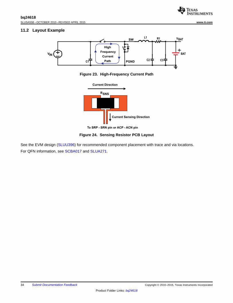
Current Direction
To SRP - SRN pin or ACP - ACN pin
RSNS
Current Sensing Direction
High
Frequency
Current
Path
L1 R1
C3C1
C2PGND
SW VBAT
BATVIN
bq24618SLUSA55B –OCTOBER 2010–REVISED APRIL 2015 www.ti.com
11.2 Layout Example
Figure 23. High-Frequency Current Path
Figure 24. Sensing Resistor PCB Layout
See the EVM design (SLUU396) for recommended component placement with trace and via locations.
For QFN information, see SCBA017 and SLUA271.
34 Submit Documentation Feedback Copyright © 2010–2015, Texas Instruments Incorporated
Product Folder Links: bq24618

bq24618www.ti.com SLUSA55B –OCTOBER 2010–REVISED APRIL 2015
12 Device and Documentation Support
12.1 Device Support
12.1.1 Third-Party Products DisclaimerTI'S PUBLICATION OF INFORMATION REGARDING THIRD-PARTY PRODUCTS OR SERVICES DOES NOTCONSTITUTE AN ENDORSEMENT REGARDING THE SUITABILITY OF SUCH PRODUCTS OR SERVICESOR A WARRANTY, REPRESENTATION OR ENDORSEMENT OF SUCH PRODUCTS OR SERVICES, EITHERALONE OR IN COMBINATION WITH ANY TI PRODUCT OR SERVICE.
12.2 Documentation Support
12.2.1 Related DocumentationFor related documentation, see the following:• EVM user's guide, SLUU396• EVM design, SLUU396• QFN information, SCBA017 and SLUA271
12.3 TrademarksAll trademarks are the property of their respective owners.
12.4 Electrostatic Discharge CautionThese devices have limited built-in ESD protection. The leads should be shorted together or the device placed in conductive foamduring storage or handling to prevent electrostatic damage to the MOS gates.
12.5 GlossarySLYZ022 — TI Glossary.
This glossary lists and explains terms, acronyms, and definitions.
13 Mechanical, Packaging, and Orderable InformationThe following pages include mechanical, packaging, and orderable information. This information is the mostcurrent data available for the designated devices. This data is subject to change without notice and revision ofthis document. For browser-based versions of this data sheet, refer to the left-hand navigation.
Copyright © 2010–2015, Texas Instruments Incorporated Submit Documentation Feedback 35
Product Folder Links: bq24618

PACKAGE OPTION ADDENDUM
www.ti.com 10-Dec-2020
Addendum-Page 1
PACKAGING INFORMATION
Orderable Device Status(1)
Package Type PackageDrawing
Pins PackageQty
Eco Plan(2)
Lead finish/Ball material
(6)
MSL Peak Temp(3)
Op Temp (°C) Device Marking(4/5)
Samples
BQ24618RGER ACTIVE VQFN RGE 24 3000 RoHS & Green NIPDAU Level-2-260C-1 YEAR -40 to 85 QWG
BQ24618RGET ACTIVE VQFN RGE 24 250 RoHS & Green NIPDAU Level-2-260C-1 YEAR -40 to 85 QWG
(1) The marketing status values are defined as follows:ACTIVE: Product device recommended for new designs.LIFEBUY: TI has announced that the device will be discontinued, and a lifetime-buy period is in effect.NRND: Not recommended for new designs. Device is in production to support existing customers, but TI does not recommend using this part in a new design.PREVIEW: Device has been announced but is not in production. Samples may or may not be available.OBSOLETE: TI has discontinued the production of the device.
(2) RoHS: TI defines "RoHS" to mean semiconductor products that are compliant with the current EU RoHS requirements for all 10 RoHS substances, including the requirement that RoHS substancedo not exceed 0.1% by weight in homogeneous materials. Where designed to be soldered at high temperatures, "RoHS" products are suitable for use in specified lead-free processes. TI mayreference these types of products as "Pb-Free".RoHS Exempt: TI defines "RoHS Exempt" to mean products that contain lead but are compliant with EU RoHS pursuant to a specific EU RoHS exemption.Green: TI defines "Green" to mean the content of Chlorine (Cl) and Bromine (Br) based flame retardants meet JS709B low halogen requirements of <=1000ppm threshold. Antimony trioxide basedflame retardants must also meet the <=1000ppm threshold requirement.
(3) MSL, Peak Temp. - The Moisture Sensitivity Level rating according to the JEDEC industry standard classifications, and peak solder temperature.
(4) There may be additional marking, which relates to the logo, the lot trace code information, or the environmental category on the device.
(5) Multiple Device Markings will be inside parentheses. Only one Device Marking contained in parentheses and separated by a "~" will appear on a device. If a line is indented then it is a continuationof the previous line and the two combined represent the entire Device Marking for that device.
(6) Lead finish/Ball material - Orderable Devices may have multiple material finish options. Finish options are separated by a vertical ruled line. Lead finish/Ball material values may wrap to twolines if the finish value exceeds the maximum column width.
Important Information and Disclaimer:The information provided on this page represents TI's knowledge and belief as of the date that it is provided. TI bases its knowledge and belief on informationprovided by third parties, and makes no representation or warranty as to the accuracy of such information. Efforts are underway to better integrate information from third parties. TI has taken andcontinues to take reasonable steps to provide representative and accurate information but may not have conducted destructive testing or chemical analysis on incoming materials and chemicals.TI and TI suppliers consider certain information to be proprietary, and thus CAS numbers and other limited information may not be available for release.
In no event shall TI's liability arising out of such information exceed the total purchase price of the TI part(s) at issue in this document sold by TI to Customer on an annual basis.
PACKAGE OPTION ADDENDUM
www.ti.com 10-Dec-2020
Addendum-Page 2
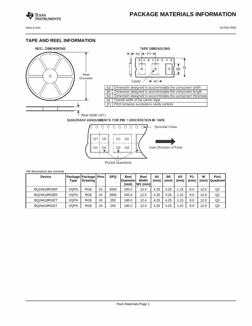
TAPE AND REEL INFORMATION
*All dimensions are nominal
Device PackageType
PackageDrawing
Pins SPQ ReelDiameter
(mm)
ReelWidth
W1 (mm)
A0(mm)
B0(mm)
K0(mm)
P1(mm)
W(mm)
Pin1Quadrant
BQ24618RGER VQFN RGE 24 3000 330.0 12.4 4.25 4.25 1.15 8.0 12.0 Q2
BQ24618RGER VQFN RGE 24 3000 330.0 12.4 4.25 4.25 1.15 8.0 12.0 Q2
BQ24618RGET VQFN RGE 24 250 180.0 12.4 4.25 4.25 1.15 8.0 12.0 Q2
BQ24618RGET VQFN RGE 24 250 180.0 12.4 4.25 4.25 1.15 8.0 12.0 Q2
PACKAGE MATERIALS INFORMATION
www.ti.com 19-Feb-2020
Pack Materials-Page 1

*All dimensions are nominal
Device Package Type Package Drawing Pins SPQ Length (mm) Width (mm) Height (mm)
BQ24618RGER VQFN RGE 24 3000 367.0 367.0 35.0
BQ24618RGER VQFN RGE 24 3000 367.0 367.0 35.0
BQ24618RGET VQFN RGE 24 250 210.0 185.0 35.0
BQ24618RGET VQFN RGE 24 250 210.0 185.0 35.0
PACKAGE MATERIALS INFORMATION
www.ti.com 19-Feb-2020
Pack Materials-Page 2
GENERIC PACKAGE VIEW
Images above are just a representation of the package family, actual package may vary.Refer to the product data sheet for package details.
RGE 24 VQFN - 1 mm max heightPLASTIC QUAD FLATPACK - NO LEAD
4204104/H

www.ti.com
PACKAGE OUTLINE
C
SEE TERMINALDETAIL
24X 0.30.2
2.45 0.1
24X 0.50.3
1 MAX
(0.2) TYP
0.050.00
20X 0.5
2X2.5
2X 2.5
A 4.13.9
B
4.13.9
0.30.2
0.50.3
VQFN - 1 mm max heightRGE0024BPLASTIC QUAD FLATPACK - NO LEAD
4219013/A 05/2017
PIN 1 INDEX AREA
0.08 C
SEATING PLANE
1
6 13
18
7 12
24 19
(OPTIONAL)PIN 1 ID
0.1 C A B0.05
EXPOSEDTHERMAL PAD
25 SYMM
SYMM
NOTES: 1. All linear dimensions are in millimeters. Any dimensions in parenthesis are for reference only. Dimensioning and tolerancing per ASME Y14.5M. 2. This drawing is subject to change without notice. 3. The package thermal pad must be soldered to the printed circuit board for thermal and mechanical performance.
SCALE 3.000
DETAILOPTIONAL TERMINAL
TYPICAL
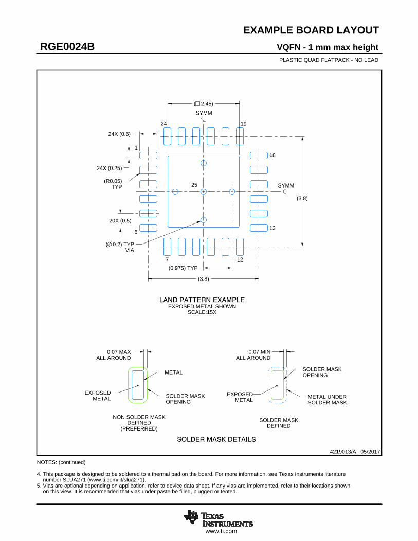
www.ti.com
EXAMPLE BOARD LAYOUT
0.07 MINALL AROUND
0.07 MAXALL AROUND
24X (0.25)
24X (0.6)
( 0.2) TYPVIA
20X (0.5)
(3.8)
(3.8)
( 2.45)
(R0.05)TYP
(0.975) TYP
VQFN - 1 mm max heightRGE0024BPLASTIC QUAD FLATPACK - NO LEAD
4219013/A 05/2017
SYMM
1
6
7 12
13
18
1924
SYMM
LAND PATTERN EXAMPLEEXPOSED METAL SHOWN
SCALE:15X
NOTES: (continued) 4. This package is designed to be soldered to a thermal pad on the board. For more information, see Texas Instruments literature number SLUA271 (www.ti.com/lit/slua271).5. Vias are optional depending on application, refer to device data sheet. If any vias are implemented, refer to their locations shown on this view. It is recommended that vias under paste be filled, plugged or tented.
25
SOLDER MASKOPENING
METAL UNDERSOLDER MASK
SOLDER MASKDEFINED
EXPOSEDMETAL
METAL
SOLDER MASKOPENING
SOLDER MASK DETAILS
NON SOLDER MASKDEFINED
(PREFERRED)
EXPOSEDMETAL

www.ti.com
EXAMPLE STENCIL DESIGN
24X (0.6)
24X (0.25)
20X (0.5)
(3.8)
(3.8)
4X ( 1.08)
(0.64)TYP
(0.64) TYP
(R0.05) TYP
VQFN - 1 mm max heightRGE0024BPLASTIC QUAD FLATPACK - NO LEAD
4219013/A 05/2017
NOTES: (continued) 6. Laser cutting apertures with trapezoidal walls and rounded corners may offer better paste release. IPC-7525 may have alternate design recommendations.
25
SYMM
METALTYP
SOLDER PASTE EXAMPLEBASED ON 0.125 mm THICK STENCIL
EXPOSED PAD 25
78% PRINTED SOLDER COVERAGE BY AREA UNDER PACKAGESCALE:20X
SYMM
1
6
7 12
13
18
1924

IMPORTANT NOTICE AND DISCLAIMER
TI PROVIDES TECHNICAL AND RELIABILITY DATA (INCLUDING DATASHEETS), DESIGN RESOURCES (INCLUDING REFERENCE DESIGNS), APPLICATION OR OTHER DESIGN ADVICE, WEB TOOLS, SAFETY INFORMATION, AND OTHER RESOURCES “AS IS” AND WITH ALL FAULTS, AND DISCLAIMS ALL WARRANTIES, EXPRESS AND IMPLIED, INCLUDING WITHOUT LIMITATION ANY IMPLIED WARRANTIES OF MERCHANTABILITY, FITNESS FOR A PARTICULAR PURPOSE OR NON-INFRINGEMENT OF THIRD PARTY INTELLECTUAL PROPERTY RIGHTS.These resources are intended for skilled developers designing with TI products. You are solely responsible for (1) selecting the appropriate TI products for your application, (2) designing, validating and testing your application, and (3) ensuring your application meets applicable standards, and any other safety, security, or other requirements. These resources are subject to change without notice. TI grants you permission to use these resources only for development of an application that uses the TI products described in the resource. Other reproduction and display of these resources is prohibited. No license is granted to any other TI intellectual property right or to any third party intellectual property right. TI disclaims responsibility for, and you will fully indemnify TI and its representatives against, any claims, damages, costs, losses, and liabilities arising out of your use of these resources.TI’s products are provided subject to TI’s Terms of Sale (www.ti.com/legal/termsofsale.html) or other applicable terms available either on ti.com or provided in conjunction with such TI products. TI’s provision of these resources does not expand or otherwise alter TI’s applicable warranties or warranty disclaimers for TI products.
Mailing Address: Texas Instruments, Post Office Box 655303, Dallas, Texas 75265Copyright © 2020, Texas Instruments Incorporated